 | ÅÙÅ£ÅçŤîîŃŧŧîÅ¿ ŤŃťŢŃŧÅçŧî: 2N5462 | ÅÀŤůîůîî:  PDF PDF  ZIP ZIP |
1
Motorola SmallÙSignal Transistors, FETs and Diodes Device Data
JFET Amplifiers
PÙChannel -- Depletion
MAXIMUM RATINGS
Rating
Symbol
Value
Unit
Drain Ù Gate Voltage
VDG
40
Vdc
Reverse Gate Ù Source Voltage
VGSR
40
Vdc
Forward Gate Current
IG(f)
10
mAdc
Total Device Dissipation @ TA = 25
¯
C
Derate above 25
¯
C
PD
350
2.8
mW
mW/
¯
C
Junction Temperature Range
TJ
Ù 65 to +135
¯
C
Storage Channel Temperature Range
Tstg
Ù 65 to +150
¯
C
ELECTRICAL CHARACTERISTICS
(TA = 25
¯
C unless otherwise noted)
Characteristic
Symbol
Min
Typ
Max
Unit
OFF CHARACTERISTICS
Gate Ù Source Breakdown Voltage
(IG = 10
ç
Adc, VDS = 0)
2N5460, 2N5461, 2N5462
V(BR)GSS
40
--
--
Vdc
Gate Reverse Current
(VGS = 20 Vdc, VDS = 0)
2N5460, 2N5461, 2N5462
(VGS = 30 Vdc, VDS = 0)
(VGS = 20 Vdc, VDS = 0, TA = 100
¯
C)
2N5460, 2N5461, 2N5462
(VGS = 30 Vdc, VDS = 0, TA = 100
¯
C)
IGSS
--
--
--
--
5.0
1.0
nAdc
ç
Adc
Gate Ù Source Cutoff Voltage
2N5460
(VDS = 15 Vdc, ID = 1.0
ç
Adc)
2N5461
2N5462
VGS(off)
0.75
1.0
1.8
--
--
--
6.0
7.5
9.0
Vdc
Gate Ù Source Voltage
(VDS = 15 Vdc, ID = 0.1 mAdc)
2N5460
(VDS = 15 Vdc, ID = 0.2 mAdc)
2N5461
(VDS = 15 Vdc, ID = 0.4 mAdc)
2N5462
VGS
0.5
0.8
1.5
--
--
--
4.0
4.5
6.0
Vdc
ON CHARACTERISTICS
Zero Ù Gate ÙVoltage Drain Current
2N5460
(VDS = 15 Vdc, VGS = 0, f = 1.0 kHz)
2N5461
2N5462
IDSS
Ù 1.0
Ù 2.0
Ù 4.0
--
--
--
Ù 5.0
Ù 9.0
Ù 16
mAdc
SMALLÙ SIGNAL CHARACTERISTICS
Forward Transfer Admittance
2N5460
(VDS = 15 Vdc, VGS = 0, f = 1.0 kHz)
2N5461
2N5462
yfs
1000
1500
2000
--
--
--
4000
5000
6000
m
mhos
Output Admittance (VDS = 15 Vdc, VGS = 0, f = 1.0 kHz)
yos
--
--
75
m
mhos
Input Capacitance (VDS = 15 Vdc, VGS = 0, f = 1.0 MHz)
Ciss
--
5.0
7.0
pF
Reverse Transfer Capacitance (VDS = 15 Vdc, VGS = 0, f = 1.0 MHz)
Crss
--
1.0
2.0
pF
FUNCTIONAL CHARACTERISTICS
Noise Figure
(VDS = 15 Vdc, VGS = 0, RG = 1.0 Megohm, f = 100 Hz, BW = 1.0 Hz)
NF
--
1.0
2.5
dB
Equivalent ShortÙCircuit Input Noise Voltage
(VDS = 15 Vdc, VGS = 0, f = 100 Hz, BW = 1.0 Hz)
en
--
60
115
nV
Hz
Order this document
by 2N5460/D
MOTOROLA
SEMICONDUCTOR TECHNICAL DATA
2N5460
thru
2N5462
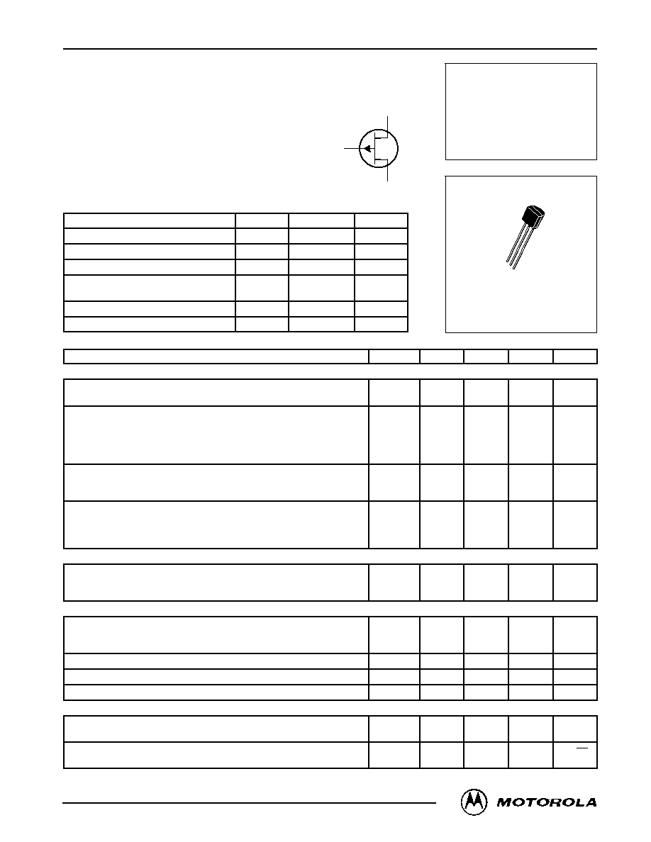
CASE 29Ù04, STYLE 7
TOÙ92 (TOÙ226AA)
1
2
3
ˋ
Motorola, Inc. 1997
2 DRAIN
1 SOURCE
3
GATE
2N5460 thru 2N5462
2
Motorola SmallÙSignal Transistors, FETs and Diodes Device Data
Y
fs
FOR
W
ARD
TRANSFER
ADMITT
ANCE
(
mhos)
m
Y
fs
FOR
W
ARD
TRANSFER
ADMITT
ANCE
(
mhos)
m
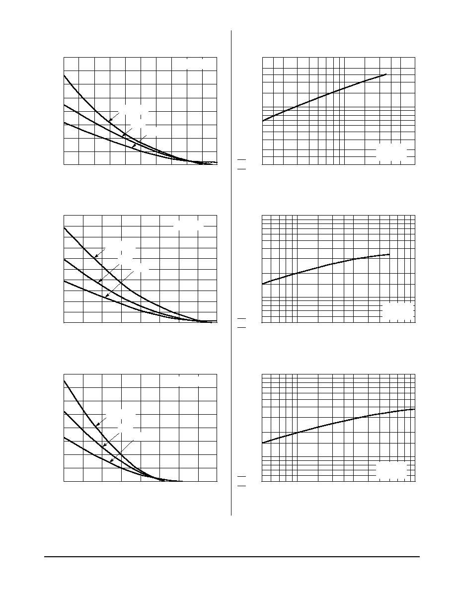
DRAIN CURRENT versus GATE
SOURCE VOLTAGE
FORWARD TRANSFER ADMITTANCE
versus DRAIN CURRENT
I D
, DRAIN CURRENT
(mA)
Y
fs
FOR
W
ARD
TRANSFER
ADMITT
ANCE
(
mhos)
m
4.0
4000
0
0.2
VGS, GATEÙSOURCE VOLTAGE (VOLTS)
Figure 1. VGS(off) = 2.0 Volts
1.0
ID, DRAIN CURRENT (mA)
3.5
I D
, DRAIN CURRENT
(mA)
10
10000
0
1.0
VGS, GATEÙSOURCE VOLTAGE (VOLTS)
Figure 2. VGS(off) = 4.0 Volts
ID, DRAIN CURRENT (mA)
I D
, DRAIN CURRENT
(mA)
16
10000
0
VGS, GATEÙSOURCE VOLTAGE (VOLTS)
Figure 3. VGS(off) = 5.0 Volts
ID, DRAIN CURRENT (mA)
Figure 4. VGS(off) = 2.0 Volts
Figure 5. VGS(off) = 4.0 Volts
Figure 6. VGS(off) = 5.0 Volts
3.0
2.5
2.0
1.5
1.0
0.5
0
0.4
0.6
0.8
1.0
1.2
1.4
1.6
1.8
2.0
VDS = 15 V
200
300
500
700
1000
2000
3000
0.2
0.3
0.5
0.7
2.0
3.0
4.0
9.0
8.0
7.0
6.0
5.0
4.0
3.0
2.0
1.0
0
0.5
1.5
2.0
2.5
3.0
3.5
4.0
500
700
1000
2000
3000
5000
7000
0.5
0.7
1.0
2.0
3.0
5.0
7.0
14
12
10
8.0
6.0
4.0
2.0
0
1.0
2.0
3.0
8.0
4.0
5.0
6.0
7.0
500
700
1000
2000
3000
5000
7000
0.5
0.7
1.0
2.0
3.0
5.0
7.0
10
TA = Ù 55
¯
C
25
¯
C
125
¯
C
VDS = 15 V
f = 1.0 kHz
VDS = 15 V
TA = Ù 55
¯
C
25
¯
C
125
¯
C
VDS = 15 V
TA = Ù 55
¯
C
25
¯
C
125
¯
C
VDS = 15 V
f = 1.0 kHz
VDS = 15 V
f = 1.0 kHz

2N5460 thru 2N5462
3
Motorola SmallÙSignal Transistors, FETs and Diodes Device Data
1000
0.1
0.2
ID, DRAIN CURRENT (mA)
Figure 7. Output Resistance
versus Drain Current
10
0.5
1.0
2.0
5.0
10
r oss
,
OUTPUT
RESIST
ANCE (k ohms)
C, CAP
ACIT
ANCE
(pF)
10
0
VDS, DRAINÙSOURCE VOLTAGE (VOLTS)
Figure 8. Capacitance versus
DrainÙSource Voltage
0
NF
, NOISE FIGURE (dB)
5.0
10
f, FREQUENCY (Hz)
Figure 9. Noise Figure versus Frequency
0
NF
, NOISE FIGURE (dB)
10
RS, SOURCE RESISTANCE (k Ohms)
Figure 10. Noise Figure versus
Source Resistance
0
Figure 11. Equivalent Low Frequency Circuit
20
30
50
70
100
200
300
500
700
1.0
2.0
3.0
4.0
5.0
6.0
7.0
8.0
9.0
10
20
30
40
4.0
3.0
2.0
1.0
20 30 50
100
200 300 500
1000 2000 3000
10,000
1.0
2.0
3.0
4.0
5.0
6.0
7.0
8.0
9.0
1.0
10
100
1000
10,000
NOTE:
1. Graphical data is presented for dc conditions. Tabular
data is given for pulsed conditions (Pulse Width = 630 ms,
Duty Cycle = 10%).
* Cosp is Coss in parallel with Series Combination of Ciss and Crss.
vi
Crss
Ciss
ross
Coss
| yfs | vi
COMMON SOURCE
y PARAMETERS FOR FREQUENCIES
BELOW 30 MHz
yis = j
Ciss
yos = j
Cosp * + 1/ross
yfs = yfs |
yrs = Ùj
Crss
VDS = 15 V
f = 1.0 kHz
IDSS = 3.0 mA
6.0 mA
10 mA
f = 1.0 MHz
VGS = 0
Ciss
Coss
Crss
VDS = 15 V
VGS = 0
RG = 1.0 Megohm
VDS = 15 V
VGS = 0
f = 100 Hz
2N5460 thru 2N5462
4
Motorola SmallÙSignal Transistors, FETs and Diodes Device Data
PACKAGE DIMENSIONS
CASE 029Ù04
(TOÙ226AA)
NOTES:
1. DIMENSIONING AND TOLERANCING PER ANSI
Y14.5M, 1982.
2. CONTROLLING DIMENSION: INCH.
3. CONTOUR OF PACKAGE BEYOND DIMENSION R
IS UNCONTROLLED.
4. DIMENSION F APPLIES BETWEEN P AND L.
DIMENSION D AND J APPLY BETWEEN L AND K
MINIMUM. LEAD DIMENSION IS UNCONTROLLED
IN P AND BEYOND DIMENSION K MINIMUM.
R
A
P
J
L
F
B
K
G
H
SECTION XÙX
C
V
D
N
N
X X
SEATING
PLANE
DIM
MIN
MAX
MIN
MAX
MILLIMETERS
INCHES
A
0.175
0.205
4.45
5.20
B
0.170
0.210
4.32
5.33
C
0.125
0.165
3.18
4.19
D
0.016
0.022
0.41
0.55
F
0.016
0.019
0.41
0.48
G
0.045
0.055
1.15
1.39
H
0.095
0.105
2.42
2.66
J
0.015
0.020
0.39
0.50
K
0.500
ÙÙÙ
12.70
ÙÙÙ
L
0.250
ÙÙÙ
6.35
ÙÙÙ
N
0.080
0.105
2.04
2.66
P
ÙÙÙ
0.100
ÙÙÙ
2.54
R
0.115
ÙÙÙ
2.93
ÙÙÙ
V
0.135
ÙÙÙ
3.43
ÙÙÙ
1
ISSUE AD
STYLE 7:
PIN 1. SOURCE
2. DRAIN
3. GATE
Motorola reserves the right to make changes without further notice to any products herein. Motorola makes no warranty, representation or guarantee regarding
the suitability of its products for any particular purpose, nor does Motorola assume any liability arising out of the application or use of any product or circuit, and
specifically disclaims any and all liability, including without limitation consequential or incidental damages. "Typical" parameters which may be provided in Motorola
data sheets and/or specifications can and do vary in different applications and actual performance may vary over time. All operating parameters, including "Typicals"
must be validated for each customer application by customer's technical experts. Motorola does not convey any license under its patent rights nor the rights of
others. Motorola products are not designed, intended, or authorized for use as components in systems intended for surgical implant into the body, or other
applications intended to support or sustain life, or for any other application in which the failure of the Motorola product could create a situation where personal injury
or death may occur. Should Buyer purchase or use Motorola products for any such unintended or unauthorized application, Buyer shall indemnify and hold Motorola
and its officers, employees, subsidiaries, affiliates, and distributors harmless against all claims, costs, damages, and expenses, and reasonable attorney fees
arising out of, directly or indirectly, any claim of personal injury or death associated with such unintended or unauthorized use, even if such claim alleges that
Motorola was negligent regarding the design or manufacture of the part. Motorola and are registered trademarks of Motorola, Inc. Motorola, Inc. is an Equal
Opportunity/Affirmative Action Employer.
Mfax is a trademark of Motorola, Inc.
How to reach us:
USA / EUROPE / Locations Not Listed: Motorola Literature Distribution;
JAPAN: Nippon Motorola Ltd.; TatsumiÙSPDÙJLDC, 6F SeibuÙButsuryuÙCenter,
P.O. Box 5405, Denver, Colorado 80217. 303Ù675Ù2140 or 1Ù800Ù441Ù2447
3Ù14Ù2 Tatsumi KotoÙKu, Tokyo 135, Japan. 81Ù3Ù3521Ù8315
Mfax
TM
: RMFAX0@email.sps.mot.com Ù TOUCHTONE 602Ù244Ù6609
ASIA/PACIFIC: Motorola Semiconductors H.K. Ltd.; 8B Tai Ping Industrial Park,
Ù US & Canada ONLY 1Ù800Ù774Ù1848
51 Ting Kok Road, Tai Po, N.T., Hong Kong. 852Ù26629298
INTERNET: http://motorola.com/sps
2N5460/D