 | –≠–ª–µ–∫—Ç—Ä–æ–Ω–Ω—ã–π –∫–æ–º–ø–æ–Ω–µ–Ω—Ç: 2N6342 | –°–∫–∞—á–∞—Ç—å:  PDF PDF  ZIP ZIP |
1
Motorola Thyristor Device Data
Triacs
Silicon Bidirectional Triode Thyristors
. . . designed primarily for full-wave ac control applications, such as light dimmers,
motor controls, heating controls and power supplies; or wherever full-wave silicon
gate controlled solid-state devices are needed. Triac type thyristors switch from a
blocking to a conducting state for either polarity of applied anode voltage with positive
or negative gate triggering.
∑
Blocking Voltage to 800 Volts
∑
All Diffused and Glass Passivated Junctions for Greater Parameter Uniformity
and Stability
∑
Small, Rugged, Thermowatt Construction for Low Thermal Resistance, High Heat
Dissipation and Durability
∑
Gate Triggering Guaranteed in Two Modes (2N6342, 2N6343, 2N6344, 2N6345)
or Four Modes (2N6346, 2N6347, 2N6348, 2N6349)
∑
For 400 Hz Operation, Consult Factory
∑
12 Ampere Devices Available as 2N6342A thru 2N6349A
MAXIMUM RATINGS
(TJ = 25
∞
C unless otherwise noted.)
Rating
Symbol
Value
Unit
*Peak Repetitive Off-State Voltage(1)
(Gate Open, TJ = ≠40 to +110
∞
C)
1/2 Sine Wave 50 to 60 Hz, Gate Open
2N6342, 2N6346
2N6343, 2N6347
2N6344, 2N6348
2N6345, 2N6349
VDRM
200
400
600
800
Volts
*RMS On-State Current
(TC = +80
∞
C)
Full Cycle Sine Wave 50 to 60 Hz
(TC = +90
∞
C)
IT(RMS)
8
4
Amps
*Peak Non-repetitive Surge Current
(One Full Cycle, 60 Hz, TC = +80
∞
C)
Preceded and followed by Rated Current
ITSM
100
Amps
Circuit Fusing
(t = 8.3 ms)
I2t
40
A2s
*Peak Gate Power (TC = +80
∞
C, Pulse Width = 2
µ
s)
PGM
20
Watts
*Average Gate Power (TC = +80
∞
C, t = 8.3 ms)
PG(AV)
0.5
Watt
*Peak Gate Current
IGM
2
Amps
*Peak Gate Voltage
VGM
10
Volts
*Operating Junction Temperature Range
TJ
≠40 to +125
∞
C
*Storage Temperature Range
Tstg
≠40 to +150
∞
C
1. VDRM for all types can be applied on a continuous basis. Blocking voltages shall not be tested with a constant current source such that the
voltage ratings of the devices are exceeded.
REV 1
Order this document
by 2N6342/D
MOTOROLA
SEMICONDUCTOR TECHNICAL DATA
©
Motorola, Inc. 1995
2N6342
thru
2N6349
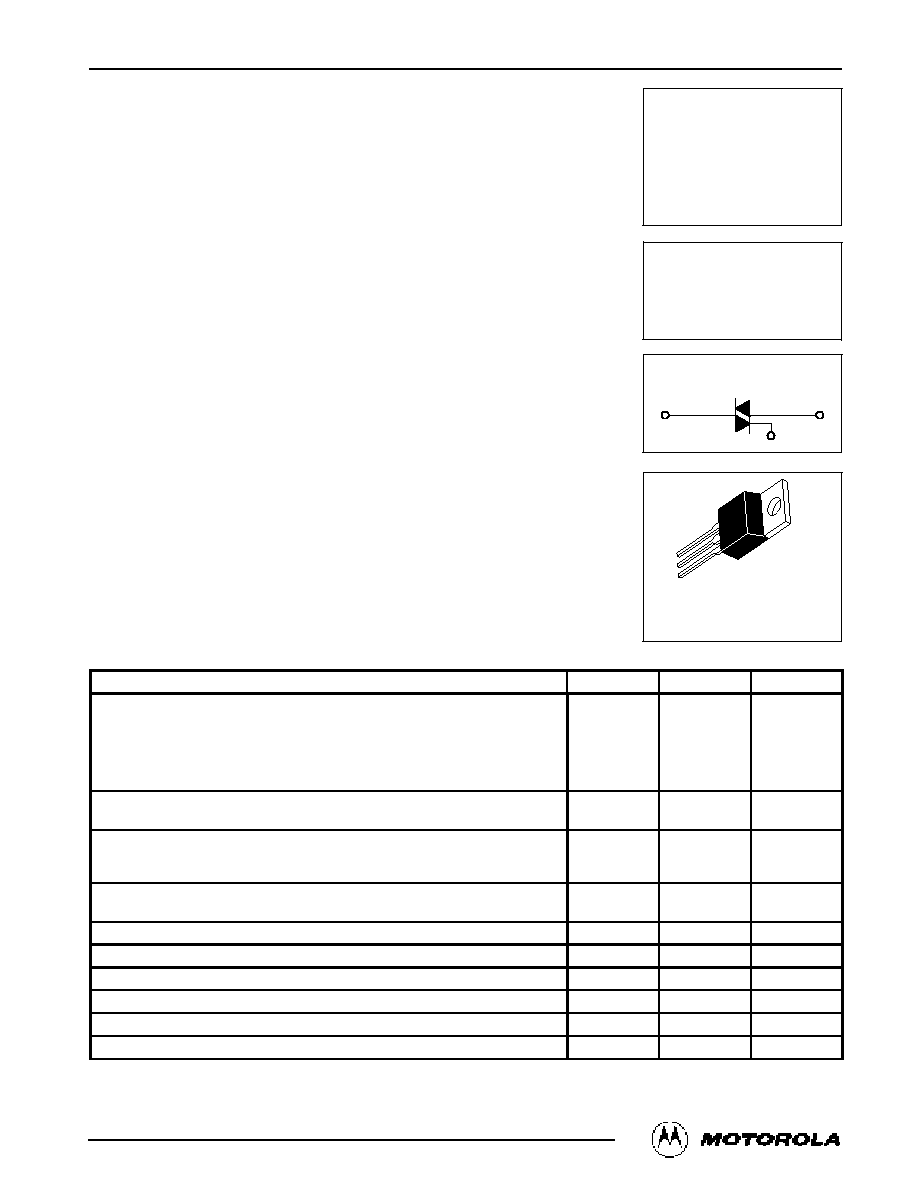
CASE 221A-04
(TO-220AB)
STYLE 4
TRIACs
8 AMPERES RMS
200 thru 800 VOLTS
MT1
G
MT2
2N6342 thru 2N6349
2
Motorola Thyristor Device Data
THERMAL CHARACTERISTICS
Characteristic
Symbol
Max
Unit
*Thermal Resistance, Junction to Case
R
JC
2.2
∞
C/W
ELECTRICAL CHARACTERISTICS
(TC = 25
∞
C, and Either Polarity of MT2 to MT1 Voltage, unless otherwise noted.)
Characteristic
Symbol
Min
Typ
Max
Unit
*Peak Blocking Current
(VD = Rated VDRM, gate open) TJ = 25
∞
C
TJ = 100
∞
C
IDRM
--
--
--
--
10
2
µ
A
mA
*Peak On-State Voltage
(ITM = 11 A Peak; Pulse Width = 1 to 2 ms, Duty Cycle
p
2%)
VTM
--
1.3
1.55
Volts
Gate Trigger Current (Continuous dc)
(VD = 12 Vdc, RL = 100 Ohms)
(Minimum Gate Pulse Width = 2
µ
s)
MT2(+), G(+) All Types
MT2(+), G(≠) 2N6346 thru 49
MT2(≠), G(≠) All Types
MT2(≠), G(+) 2N6346 thru 49
*MT2(+), G(+); MT2(≠), G(≠) TC = ≠40
∞
C All Types
*MT2(+), G(≠); MT2(≠), G(+) TC = ≠40
∞
C 2N6346 thru 49
IGT
--
--
--
--
--
--
12
12
20
35
--
--
50
75
50
75
100
125
mA
Gate Trigger Voltage (Continuous dc)
(VD = 12 Vdc, RL = 100 Ohms)
(Minimum Gate Pulse Width = 2
µ
s)
MT2(+), G(+) All Types
MT2(+), G(≠) 2N6346 thru 49
MT2(≠), G(≠) All Types
MT2(≠), G(+) 2N6346 thru 49
*MT2(+), G(+); MT2(≠), G(≠) TC = ≠40
∞
C All Types
*MT2(+), G(≠); MT2(≠), G(+) TC = ≠40
∞
C 2N6346 thru 49
(VD = Rated VDRM, RL = 10 k Ohms, TJ = 100
∞
C)
*MT2(+), G(+); MT2(≠), G(≠) All Types
*MT2(+), G(≠); MT2(≠), G(≠) 2N6346 thru 49
VGT
--
--
--
--
--
--
0.2
0.2
0.9
0.9
1.1
1.4
--
--
--
--
2
2.5
2
2.5
2.5
3
--
--
Volts
*Holding Current
(VD = 12 Vdc, Gate Open)
TC = 25
∞
C
(IT = 200 mA)
*TC = ≠40
∞
C
IH
--
--
6
--
40
75
mA
*Turn-On Time
(VD = Rated VDRM, ITM = 11 A, IGT = 120 mA,
Rise Time = 0.1
µ
s, Pulse Width = 2
µ
s)
tgt
--
1.5
2
µ
s
Critical Rate of Rise of Commutation Voltage
(VD = Rated VDRM, ITM = 11 A, Commutating di/dt = 4.0 A/ms,
Gate Unenergized, TC = 80
∞
C)
dv/dt(c)
--
5
--
V/
µ
s
*Indicates JEDEC Registered Data.
2.0
4.0
6.0
8.0
10
3.0
7.0
6.0
5.0
4.0
1.0
2.0
0
0
IT(RMS), RMS ON-STATE CURRENT (AMP)
dc
30
∞
60
∞
90
∞
120
∞
= 180
∞
TJ
[
100
∞
C
8.0
= CONDUCTION ANGLE
P
,
A
VERAGE POWER (W
A
TTS)
(A
V)
FIGURE 1 ≠ RMS CURRENT DERATING
FIGURE 2 ≠ ON-STATE POWER DISSIPATION
1.0
2.0
3.0
4.0
5.0
6.0
7.0
96
92
88
84
80
= CONDUCTION ANGLE
IT(RMS), RMS ON-STATE CURRENT (AMP)
100
8.0
0
dc
= 30
∞
60
∞
90
∞
120
∞
180
∞
T
, CASE
TEMPERA
TURE ( C)
C
∞
2N6342 thru 2N6349
3
Motorola Thyristor Device Data
≠20
70
100
50
30
20
2.0
10
7.0
5.0
3.0
1.0
0.7
0.5
0.3
0.2
4.4
4.0
3.6
3.2
2.8
2.4
2.0
1.6
1.2
1.8
1.6
1.4
1.2
1.0
0.8
0.6
≠40
3.0
5.0
7.0
10
20
0.4
0.4
0.8
≠40
vTM, INSTANTANEOUS ON-STATE VOLTAGE (VOLTS)
25
∞
C
0.1
TJ = 100
∞
C
TJ, JUNCTION TEMPERATURE (
∞
C)
140
120
100
80
60
40
0
≠20
20
≠60
QUADRANT 4
3
2
1
50
30
20
10
7.0
5.0
140
120
100
80
60
40
20
0
≠20
≠40
≠60
OFF-STATE VOLTAGE = 12 V
1
TJ, JUNCTION TEMPERATURE (
∞
C)
2.0
MAIN TERMINAL #2
POSITIVE
60
120
TJ, JUNCTION TEMPERATURE (
∞
C)
140
80
100
40
0
20
≠60
100
80
60
40
20
NUMBER OF CYCLES
10
7.0
5.0
3.0
2.0
0
1.0
TJ = 100
∞
C
f = 60 Hz
CYCLE
2
4
3
QUADRANT
OFF-STATE VOLTAGE = 12 V
Surge is preceded and followed by rated current
MAIN TERMINAL #1
POSITIVE
V , GA
TE
TRIGGER VOL
T
AGE (VOL
TS)
gt
I , GA
TE
TRIGGER CURRENT
(mA)
GT
i , INST
ANT
ANEOUS ON-ST
A
TE CURRENT
(AMP)
TM
I , PEAK SURGE CURRENT
(AMP)
TSM
I , HOLDING CURRENT
(mA)
H
FIGURE 3 ≠ TYPICAL GATE TRIGGER VOLTAGE
FIGURE 4 ≠ TYPICAL GATE TRIGGER CURRENT
FIGURE 5 ≠ ON-STATE CHARACTERISTICS
FIGURE 6 ≠ TYPICAL HOLDING CURRENT
FIGURE 7 ≠ MAXIMUM NON-REPETITIVE SURGE CURRENT
QUADRANTS
GATE OPEN
2N6342 thru 2N6349
4
Motorola Thyristor Device Data
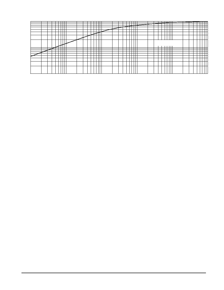
0.02
0.05
0.1
0.2
0.5
1.0
0.2
0.5
1.0
100
200
500
50
5.0 k
2.0 k
1.0 k
20
5.0
10 k
2.0
Z
JC(t) = r(t)
∑
R
JC
0.01
0.1
t,TIME (ms)
r(t),
TRANSIENT
THERMAL
RESIST
ANCE
(NORMALIZED)
FIGURE 8 ≠ TYPICAL THERMAL RESPONSE

2N6342 thru 2N6349
5
Motorola Thyristor Device Data
PACKAGE DIMENSIONS
NOTES:
1. DIMENSIONING AND TOLERANCING PER ANSI
Y14.5M, 1982.
2. CONTROLLING DIMENSION: INCH.
3. DIMENSION Z DEFINES A ZONE WHERE ALL
BODY AND LEAD IRREGULARITIES ARE
ALLOWED.
STYLE 4:
PIN 1. MAIN TERMINAL 1
2. MAIN TERMINAL 2
3. GATE
4. MAIN TERMINAL 2
DIM
MIN
MAX
MIN
MAX
MILLIMETERS
INCHES
A
0.570
0.620
14.48
15.75
B
0.380
0.405
9.66
10.28
C
0.160
0.190
4.07
4.82
D
0.025
0.035
0.64
0.88
F
0.142
0.147
3.61
3.73
G
0.095
0.105
2.42
2.66
H
0.110
0.155
2.80
3.93
J
0.014
0.022
0.36
0.55
K
0.500
0.562
12.70
14.27
L
0.045
0.055
1.15
1.39
N
0.190
0.210
4.83
5.33
Q
0.100
0.120
2.54
3.04
R
0.080
0.110
2.04
2.79
S
0.045
0.055
1.15
1.39
T
0.235
0.255
5.97
6.47
U
0.000
0.050
0.00
1.27
V
0.045
≠≠≠
1.15
≠≠≠
Z
≠≠≠
0.080
≠≠≠
2.04
A
K
L
V
G
D
N
Z
H
Q
F
B
1
2
3
4
≠T≠
SEATING
PLANE
S
R
J
U
T
C
CASE 221A-04
(TO≠220AB)

2N6342 thru 2N6349
6
Motorola Thyristor Device Data
Motorola reserves the right to make changes without further notice to any products herein. Motorola makes no warranty, representation or guarantee regarding
the suitability of its products for any particular purpose, nor does Motorola assume any liability arising out of the application or use of any product or circuit, and
specifically disclaims any and all liability, including without limitation consequential or incidental damages. "Typical" parameters can and do vary in different
applications. All operating parameters, including "Typicals" must be validated for each customer application by customer's technical experts. Motorola does
not convey any license under its patent rights nor the rights of others. Motorola products are not designed, intended, or authorized for use as components in
systems intended for surgical implant into the body, or other applications intended to support or sustain life, or for any other application in which the failure of
the Motorola product could create a situation where personal injury or death may occur. Should Buyer purchase or use Motorola products for any such
unintended or unauthorized application, Buyer shall indemnify and hold Motorola and its officers, employees, subsidiaries, affiliates, and distributors harmless
against all claims, costs, damages, and expenses, and reasonable attorney fees arising out of, directly or indirectly, any claim of personal injury or death
associated with such unintended or unauthorized use, even if such claim alleges that Motorola was negligent regarding the design or manufacture of the part.
Motorola and
are registered trademarks of Motorola, Inc. Motorola, Inc. is an Equal Opportunity/Affirmative Action Employer.
Literature Distribution Centers:
USA: Motorola Literature Distribution; P.O. Box 20912; Phoenix, Arizona 85036.
EUROPE: Motorola Ltd.; European Literature Centre; 88 Tanners Drive, Blakelands, Milton Keynes, MK14 5BP, England.
JAPAN: Nippon Motorola Ltd.; 4-32-1, Nishi-Gotanda, Shinagawa-ku, Tokyo 141, Japan.
ASIA PACIFIC: Motorola Semiconductors H.K. Ltd.; Silicon Harbour Center, No. 2 Dai King Street, Tai Po Industrial Estate, Tai Po, N.T., Hong Kong.
2N6342/D
*2N6342/D*