 | –≠–ª–µ–∫—Ç—Ä–æ–Ω–Ω—ã–π –∫–æ–º–ø–æ–Ω–µ–Ω—Ç: 54HC74 | –°–∫–∞—á–∞—Ç—å:  PDF PDF  ZIP ZIP |
MOTOROLA
SEMICONDUCTOR TECHNICAL DATA
1
REV 1
©
Motorola, Inc. 1997
6/97
Dual D-Type Flip-Flop
with Set and Reset
The MC74VHC74 is an advanced high speed CMOS D≠type flip≠flop
fabricated with silicon gate CMOS technology. It achieves high speed
operation similar to equivalent Bipolar Schottky TTL while maintaining
CMOS low power dissipation.
The signal level applied to the D input is transferred to Q output during the
positive going transition of the Clock pulse.
Reset (RD) and Set (SD) are independent of the Clock (CP) and are
accomplished by setting the appropriate input Low.
The internal circuit is composed of three stages, including a buffer output
which provides high noise immunity and stable output. The inputs tolerate
voltages up to 7V, allowing the interface of 5V systems to 3V systems.
∑
High Speed: fmax = 170MHz (Typ) at VCC = 5V
∑
Low Power Dissipation: ICC = 2
µ
A (Max) at TA = 25
∞
C
∑
High Noise Immunity: VNIH = VNIL = 28% VCC
∑
Power Down Protection Provided on Inputs
∑
Balanced Propagation Delays
∑
Designed for 2V to 5.5V Operating Range
∑
Low Noise: VOLP = 0.8V (Max)
∑
Pin and Function Compatible with Other Standard Logic Families
∑
Latchup Performance Exceeds 300mA
∑
ESD Performance: HBM > 2000V; Machine Model > 200V
∑
Chip Complexity: 128 FETs or 32 Equivalent Gates
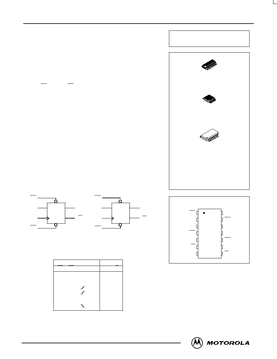
LOGIC DIAGRAM
RD1
D1
CP1
SD1
RD2
D2
CP2
SD2
1
2
3
4
13
12
11
10
5
6
9
8
Q1
Q1
Q2
Q2
FUNCTION TABLE
Inputs
Outputs
SD
RD
CP
D
Q
Q
L
H
X
X
H
L
H
L
X
X
L
H
L
L
X
X
H*
H*
H
H
H
H
L
H
H
L
L
H
H
H
L
X
No Change
H
H
H
X
No Change
H
H
X
No Change
* Both outputs will remain high as long as Set and Reset are low, but the output
states are unpredictable if Set and Reset go high simultaneously.
MC74VHC74
PIN ASSIGNMENT
SD1
CP1
D1
RD1
11
12
13
14
8
9
10
5
4
3
2
1
7
6
SD2
CP2
D2
RD2
VCC
Q2
Q2
GND
Q1
Q1
D SUFFIX
14≠LEAD SOIC PACKAGE
CASE 751A≠03
DT SUFFIX
14≠LEAD TSSOP PACKAGE
CASE 948G≠01
ORDERING INFORMATION
MC74VHCXXD
MC74VHCXXDT
MC74VHCXXM
SOIC
TSSOP
SOIC EIAJ
M SUFFIX
14≠LEAD SOIC EIAJ PACKAGE
CASE 965≠01
MC74VHC74
MOTOROLA
VHC Data ≠ Advanced CMOS Logic
DL203 -- Rev 1
2
ŒŒŒŒŒŒŒŒŒŒŒŒŒŒŒŒŒŒŒŒŒŒŒ
ŒŒŒŒŒŒŒŒŒŒŒŒŒŒŒŒŒŒŒŒŒŒŒ
MAXIMUM RATINGS*
ŒŒŒ
ŒŒŒ
Symbol
ŒŒŒŒŒŒŒŒŒŒŒŒŒŒ
ŒŒŒŒŒŒŒŒŒŒŒŒŒŒ
Parameter
ŒŒŒŒŒŒ
ŒŒŒŒŒŒ
Value
ŒŒŒ
ŒŒŒ
Unit
ŒŒŒ
ŒŒŒ
VCC
ŒŒŒŒŒŒŒŒŒŒŒŒŒŒ
ŒŒŒŒŒŒŒŒŒŒŒŒŒŒ
DC Supply Voltage
ŒŒŒŒŒŒ
ŒŒŒŒŒŒ
≠ 0.5 to + 7.0
ŒŒŒ
ŒŒŒ
V
ŒŒŒ
ŒŒŒ
Vin
ŒŒŒŒŒŒŒŒŒŒŒŒŒŒ
ŒŒŒŒŒŒŒŒŒŒŒŒŒŒ
DC Input Voltage
ŒŒŒŒŒŒ
ŒŒŒŒŒŒ
≠ 0.5 to + 7.0
ŒŒŒ
ŒŒŒ
V
ŒŒŒ
ŒŒŒ
Vout
ŒŒŒŒŒŒŒŒŒŒŒŒŒŒ
ŒŒŒŒŒŒŒŒŒŒŒŒŒŒ
DC Output Voltage
ŒŒŒŒŒŒ
ŒŒŒŒŒŒ
≠ 0.5 to VCC + 0.5
ŒŒŒ
ŒŒŒ
V
ŒŒŒ
ŒŒŒ
IIK
ŒŒŒŒŒŒŒŒŒŒŒŒŒŒ
ŒŒŒŒŒŒŒŒŒŒŒŒŒŒ
Input Diode Current
ŒŒŒŒŒŒ
ŒŒŒŒŒŒ
≠ 20
ŒŒŒ
ŒŒŒ
mA
ŒŒŒ
ŒŒŒ
IOK
ŒŒŒŒŒŒŒŒŒŒŒŒŒŒ
ŒŒŒŒŒŒŒŒŒŒŒŒŒŒ
Output Diode Current
ŒŒŒŒŒŒ
ŒŒŒŒŒŒ
±
20
ŒŒŒ
ŒŒŒ
mA
ŒŒŒ
ŒŒŒ
Iout
ŒŒŒŒŒŒŒŒŒŒŒŒŒŒ
ŒŒŒŒŒŒŒŒŒŒŒŒŒŒ
DC Output Current, per Pin
ŒŒŒŒŒŒ
ŒŒŒŒŒŒ
±
25
ŒŒŒ
ŒŒŒ
mA
ŒŒŒ
ŒŒŒ
ICC
ŒŒŒŒŒŒŒŒŒŒŒŒŒŒ
ŒŒŒŒŒŒŒŒŒŒŒŒŒŒ
DC Supply Current, VCC and GND Pins
ŒŒŒŒŒŒ
ŒŒŒŒŒŒ
±
50
ŒŒŒ
ŒŒŒ
mA
ŒŒŒ
Œ
Œ
Œ
ŒŒŒ
PD
ŒŒŒŒŒŒŒŒŒŒŒŒŒŒ
Œ
ŒŒŒŒŒŒŒŒŒŒŒŒ
Œ
ŒŒŒŒŒŒŒŒŒŒŒŒŒŒ
Power Dissipation in Still Air,
SOIC Packages
TSSOP Package
ŒŒŒŒŒŒ
Œ
ŒŒŒŒ
Œ
ŒŒŒŒŒŒ
500
450
ŒŒŒ
Œ
Œ
Œ
ŒŒŒ
mW
ŒŒŒ
ŒŒŒ
Tstg
ŒŒŒŒŒŒŒŒŒŒŒŒŒŒ
ŒŒŒŒŒŒŒŒŒŒŒŒŒŒ
Storage Temperature
ŒŒŒŒŒŒ
ŒŒŒŒŒŒ
≠ 65 to + 150
ŒŒŒ
ŒŒŒ
_
C
* Absolute maximum continuous ratings are those values beyond which damage to the device
may occur. Exposure to these conditions or conditions beyond those indicated may adversely
affect device reliability. Functional operation under absolute≠maximum≠rated conditions is not
implied.
Derating -- SOIC Packages: ≠ 7 mW/
_
C from 65
_
to 125
_
C
TSSOP Package: ≠ 6.1 mW/
_
C from 65
_
to 125
_
C
RECOMMENDED OPERATING CONDITIONS
ŒŒŒŒ
ŒŒŒŒ
Symbol
ŒŒŒŒŒŒŒŒŒŒŒŒŒŒ
ŒŒŒŒŒŒŒŒŒŒŒŒŒŒ
Parameter
ŒŒŒ
ŒŒŒ
Min
ŒŒŒ
ŒŒŒ
Max
ŒŒŒ
ŒŒŒ
Unit
ŒŒŒŒ
ŒŒŒŒ
VCC
ŒŒŒŒŒŒŒŒŒŒŒŒŒŒ
ŒŒŒŒŒŒŒŒŒŒŒŒŒŒ
DC Supply Voltage
ŒŒŒ
ŒŒŒ
2.0
ŒŒŒ
ŒŒŒ
5.5
ŒŒŒ
ŒŒŒ
V
ŒŒŒŒ
ŒŒŒŒ
Vin
ŒŒŒŒŒŒŒŒŒŒŒŒŒŒ
ŒŒŒŒŒŒŒŒŒŒŒŒŒŒ
DC Input Voltage
ŒŒŒ
ŒŒŒ
0
ŒŒŒ
ŒŒŒ
5.5
ŒŒŒ
ŒŒŒ
V
ŒŒŒŒ
ŒŒŒŒ
Vout
ŒŒŒŒŒŒŒŒŒŒŒŒŒŒ
ŒŒŒŒŒŒŒŒŒŒŒŒŒŒ
DC Output Voltage
ŒŒŒ
ŒŒŒ
0
ŒŒŒ
ŒŒŒ
VCC
ŒŒŒ
ŒŒŒ
V
ŒŒŒŒ
ŒŒŒŒ
TA
ŒŒŒŒŒŒŒŒŒŒŒŒŒŒ
ŒŒŒŒŒŒŒŒŒŒŒŒŒŒ
Operating Temperature, All Package Types
ŒŒŒ
ŒŒŒ
≠ 40
ŒŒŒ
ŒŒŒ
+ 85
ŒŒŒ
ŒŒŒ
_
C
ŒŒŒŒ
ŒŒŒŒ
tr, tf
ŒŒŒŒŒŒŒŒŒŒŒŒŒŒ
ŒŒŒŒŒŒŒŒŒŒŒŒŒŒ
Input Rise and Fall Time
VCC = 3.3V
±
0.3V
VCC =5.0V
±
0.5V
ŒŒŒ
ŒŒŒ
0
0
ŒŒŒ
ŒŒŒ
100
20
ŒŒŒ
ŒŒŒ
ns/V
ŒŒŒŒŒŒŒŒŒŒŒŒŒŒŒŒŒŒŒŒŒŒŒŒŒŒŒŒŒŒŒŒŒ
ŒŒŒŒŒŒŒŒŒŒŒŒŒŒŒŒŒŒŒŒŒŒŒŒŒŒŒŒŒŒŒŒŒ
DC ELECTRICAL CHARACTERISTICS
ŒŒŒŒ
ŒŒŒŒ
S
b l
ŒŒŒŒŒŒ
ŒŒŒŒŒŒ
P
ŒŒŒŒŒŒŒŒ
ŒŒŒŒŒŒŒŒ
T
C
di i
ŒŒŒ
ŒŒŒ
VCC
ŒŒŒŒŒŒŒŒŒ
ŒŒŒŒŒŒŒŒŒ
TA = 25
∞
C
ŒŒŒŒŒŒŒ
ŒŒŒŒŒŒŒ
TA = ≠ 40 to 85
∞
C
ŒŒ
ŒŒ
U i
ŒŒŒŒ
ŒŒŒŒ
Symbol
ŒŒŒŒŒŒ
ŒŒŒŒŒŒ
Parameter
ŒŒŒŒŒŒŒŒ
ŒŒŒŒŒŒŒŒ
Test Conditions
ŒŒŒ
ŒŒŒ
VCC
V
ŒŒŒŒ
ŒŒŒŒ
Min
ŒŒŒ
ŒŒŒ
Typ
ŒŒŒŒ
ŒŒŒŒ
Max
ŒŒŒŒ
ŒŒŒŒ
Min
ŒŒŒŒ
ŒŒŒŒ
Max
ŒŒ
ŒŒ
Unit
ŒŒŒŒ
Œ
ŒŒ
Œ
ŒŒŒŒ
VIH
ŒŒŒŒŒŒ
Œ
ŒŒŒŒ
Œ
ŒŒŒŒŒŒ
Minimum High≠Level
Input Voltage
ŒŒŒŒŒŒŒŒ
Œ
ŒŒŒŒŒŒ
Œ
ŒŒŒŒŒŒŒŒ
ŒŒŒ
ŒŒ
Œ
ŒŒŒ
2.0
3.0 to
5.5
ŒŒŒŒ
Œ
ŒŒ
Œ
ŒŒŒŒ
1.50
VCC x 0.7
ŒŒŒ
Œ
Œ
Œ
ŒŒŒ
ŒŒŒŒ
Œ
ŒŒ
Œ
ŒŒŒŒ
ŒŒŒŒ
Œ
ŒŒ
Œ
ŒŒŒŒ
1.50
VCC x 0.7
ŒŒŒŒ
Œ
ŒŒ
Œ
ŒŒŒŒ
ŒŒ
ŒŒ
ŒŒ
V
ŒŒŒŒ
Œ
ŒŒ
Œ
Œ
ŒŒ
Œ
ŒŒŒŒ
VIL
ŒŒŒŒŒŒ
Œ
ŒŒŒŒ
Œ
Œ
ŒŒŒŒ
Œ
ŒŒŒŒŒŒ
Maximum Low≠Level
Input Voltage
ŒŒŒŒŒŒŒŒ
Œ
ŒŒŒŒŒŒ
Œ
Œ
ŒŒŒŒŒŒ
Œ
ŒŒŒŒŒŒŒŒ
ŒŒŒ
ŒŒ
Œ
ŒŒ
Œ
ŒŒŒ
2.0
3.0 to
5.5
ŒŒŒŒ
Œ
ŒŒ
Œ
Œ
ŒŒ
Œ
ŒŒŒŒ
ŒŒŒ
Œ
Œ
Œ
Œ
Œ
Œ
ŒŒŒ
ŒŒŒŒ
Œ
ŒŒ
Œ
Œ
ŒŒ
Œ
ŒŒŒŒ
0.50
VCC x 0.3
ŒŒŒŒ
Œ
ŒŒ
Œ
Œ
ŒŒ
Œ
ŒŒŒŒ
ŒŒŒŒ
Œ
ŒŒ
Œ
Œ
ŒŒ
Œ
ŒŒŒŒ
0.50
VCC x 0.3
ŒŒ
ŒŒ
ŒŒ
ŒŒ
V
ŒŒŒŒ
Œ
ŒŒ
Œ
Œ
ŒŒ
Œ
ŒŒŒŒ
VOH
ŒŒŒŒŒŒ
Œ
ŒŒŒŒ
Œ
Œ
ŒŒŒŒ
Œ
ŒŒŒŒŒŒ
Minimum High≠Level
Output Voltage
ŒŒŒŒŒŒŒŒ
Œ
ŒŒŒŒŒŒ
Œ
Œ
ŒŒŒŒŒŒ
Œ
ŒŒŒŒŒŒŒŒ
Vin = VIH or VIL
IOH = ≠ 50
µ
A
ŒŒŒ
ŒŒ
Œ
ŒŒ
Œ
ŒŒŒ
2.0
3.0
4.5
ŒŒŒŒ
Œ
ŒŒ
Œ
Œ
ŒŒ
Œ
ŒŒŒŒ
1.9
2.9
4.4
ŒŒŒ
Œ
Œ
Œ
Œ
Œ
Œ
ŒŒŒ
2.0
3.0
4.5
ŒŒŒŒ
Œ
ŒŒ
Œ
Œ
ŒŒ
Œ
ŒŒŒŒ
ŒŒŒŒ
Œ
ŒŒ
Œ
Œ
ŒŒ
Œ
ŒŒŒŒ
1.9
2.9
4.4
ŒŒŒŒ
Œ
ŒŒ
Œ
Œ
ŒŒ
Œ
ŒŒŒŒ
ŒŒ
ŒŒ
ŒŒ
ŒŒ
V
ŒŒŒŒ
Œ
ŒŒ
Œ
ŒŒŒŒ
ŒŒŒŒŒŒ
Œ
ŒŒŒŒ
Œ
ŒŒŒŒŒŒ
ŒŒŒŒŒŒŒŒ
Œ
ŒŒŒŒŒŒ
Œ
ŒŒŒŒŒŒŒŒ
Vin = VIH or VIL
IOH = ≠ 4mA
IOH = ≠ 8mA
ŒŒŒ
ŒŒ
Œ
ŒŒŒ
3.0
4.5
ŒŒŒŒ
Œ
ŒŒ
Œ
ŒŒŒŒ
2.58
3.94
ŒŒŒ
Œ
Œ
Œ
ŒŒŒ
ŒŒŒŒ
Œ
ŒŒ
Œ
ŒŒŒŒ
ŒŒŒŒ
Œ
ŒŒ
Œ
ŒŒŒŒ
2.48
3.80
ŒŒŒŒ
Œ
ŒŒ
Œ
ŒŒŒŒ
ŒŒ
ŒŒ
ŒŒ
ŒŒŒŒ
Œ
ŒŒ
Œ
Œ
ŒŒ
Œ
VOL
ŒŒŒŒŒŒ
Œ
ŒŒŒŒ
Œ
Œ
ŒŒŒŒ
Œ
Maximum Low≠Level
Output Voltage
ŒŒŒŒŒŒŒŒ
Œ
ŒŒŒŒŒŒ
Œ
Œ
ŒŒŒŒŒŒ
Œ
Vin = VIH or VIL
IOL = 50
µ
A
ŒŒŒ
ŒŒ
Œ
ŒŒ
Œ
2.0
3.0
4.5
ŒŒŒŒ
Œ
ŒŒ
Œ
Œ
ŒŒ
Œ
ŒŒŒ
Œ
Œ
Œ
Œ
Œ
Œ
0.0
0.0
0.0
ŒŒŒŒ
Œ
ŒŒ
Œ
Œ
ŒŒ
Œ
0.1
0.1
0.1
ŒŒŒŒ
Œ
ŒŒ
Œ
Œ
ŒŒ
Œ
ŒŒŒŒ
Œ
ŒŒ
Œ
Œ
ŒŒ
Œ
0.1
0.1
0.1
ŒŒ
ŒŒ
ŒŒ
V
ŒŒŒŒ
Œ
ŒŒ
Œ
Œ
ŒŒ
Œ
ŒŒŒŒ
ŒŒŒŒŒŒ
Œ
ŒŒŒŒ
Œ
Œ
ŒŒŒŒ
Œ
ŒŒŒŒŒŒ
ŒŒŒŒŒŒŒŒ
Œ
ŒŒŒŒŒŒ
Œ
Œ
ŒŒŒŒŒŒ
Œ
ŒŒŒŒŒŒŒŒ
Vin = VIH or VIL
IOL = 4mA
IOL = 8mA
ŒŒŒ
ŒŒ
Œ
ŒŒ
Œ
ŒŒŒ
3.0
4.5
ŒŒŒŒ
Œ
ŒŒ
Œ
Œ
ŒŒ
Œ
ŒŒŒŒ
ŒŒŒ
Œ
Œ
Œ
Œ
Œ
Œ
ŒŒŒ
ŒŒŒŒ
Œ
ŒŒ
Œ
Œ
ŒŒ
Œ
ŒŒŒŒ
0.36
0.36
ŒŒŒŒ
Œ
ŒŒ
Œ
Œ
ŒŒ
Œ
ŒŒŒŒ
ŒŒŒŒ
Œ
ŒŒ
Œ
Œ
ŒŒ
Œ
ŒŒŒŒ
0.44
0.44
ŒŒ
ŒŒ
ŒŒ
ŒŒ
This device contains protection
circuitry to guard against damage
due to high static voltages or electric
fields. However, precautions must
be taken to avoid applications of any
voltage higher than maximum rated
voltages to this high≠impedance cir-
cuit. For proper operation, Vin and
Vout should be constrained to the
range GND
v
(Vin or Vout)
v
VCC.
Unused inputs must always be
tied to an appropriate logic voltage
level (e.g., either GND or VCC).
Unused outputs must be left open.
MC74VHC74
VHC Data ≠ Advanced CMOS Logic
DL203 -- Rev 1
3
MOTOROLA
ŒŒŒŒŒŒŒŒŒŒŒŒŒŒŒŒŒŒŒŒŒŒŒŒŒŒŒŒŒŒŒŒŒ
ŒŒŒŒŒŒŒŒŒŒŒŒŒŒŒŒŒŒŒŒŒŒŒŒŒŒŒŒŒŒŒŒŒ
DC ELECTRICAL CHARACTERISTICS
ŒŒ
ŒŒ
Unit
ŒŒŒŒŒŒŒ
ŒŒŒŒŒŒŒ
TA = ≠ 40 to 85
∞
C
ŒŒŒŒŒŒŒŒŒ
ŒŒŒŒŒŒŒŒŒ
TA = 25
∞
C
ŒŒŒ
ŒŒŒ
VCC
V
ŒŒŒŒŒŒŒŒ
ŒŒŒŒŒŒŒŒ
Test Conditions
ŒŒŒŒŒŒ
ŒŒŒŒŒŒ
Parameter
ŒŒŒŒ
ŒŒŒŒ
Symbol
ŒŒ
ŒŒ
Unit
ŒŒŒŒ
ŒŒŒŒ
Max
ŒŒŒŒ
ŒŒŒŒ
Min
ŒŒŒŒ
ŒŒŒŒ
Max
ŒŒŒ
ŒŒŒ
Typ
ŒŒŒŒ
ŒŒŒŒ
Min
ŒŒŒ
ŒŒŒ
VCC
V
ŒŒŒŒŒŒŒŒ
ŒŒŒŒŒŒŒŒ
Test Conditions
ŒŒŒŒŒŒ
ŒŒŒŒŒŒ
Parameter
ŒŒŒŒ
ŒŒŒŒ
Symbol
ŒŒŒŒ
Œ
ŒŒ
Œ
ŒŒŒŒ
Iin
ŒŒŒŒŒŒ
Œ
ŒŒŒŒ
Œ
ŒŒŒŒŒŒ
Maximum Input
Leakage Current
ŒŒŒŒŒŒŒŒ
Œ
ŒŒŒŒŒŒ
Œ
ŒŒŒŒŒŒŒŒ
Vin = 5.5V or GND
ŒŒŒ
ŒŒ
Œ
ŒŒŒ
0 to 5.5
ŒŒŒŒ
Œ
ŒŒ
Œ
ŒŒŒŒ
ŒŒŒ
Œ
Œ
Œ
ŒŒŒ
ŒŒŒŒ
Œ
ŒŒ
Œ
ŒŒŒŒ
±
0.1
ŒŒŒŒ
Œ
ŒŒ
Œ
ŒŒŒŒ
ŒŒŒŒ
Œ
ŒŒ
Œ
ŒŒŒŒ
±
1.0
ŒŒ
ŒŒ
ŒŒ
µ
A
ŒŒŒŒ
Œ
ŒŒ
Œ
ŒŒŒŒ
ICC
ŒŒŒŒŒŒ
Œ
ŒŒŒŒ
Œ
ŒŒŒŒŒŒ
Maximum Quiescent
Supply Current
ŒŒŒŒŒŒŒŒ
Œ
ŒŒŒŒŒŒ
Œ
ŒŒŒŒŒŒŒŒ
Vin = VCC or GND
ŒŒŒ
ŒŒ
Œ
ŒŒŒ
5.5
ŒŒŒŒ
Œ
ŒŒ
Œ
ŒŒŒŒ
ŒŒŒ
Œ
Œ
Œ
ŒŒŒ
ŒŒŒŒ
Œ
ŒŒ
Œ
ŒŒŒŒ
2.0
ŒŒŒŒ
Œ
ŒŒ
Œ
ŒŒŒŒ
ŒŒŒŒ
Œ
ŒŒ
Œ
ŒŒŒŒ
20.0
ŒŒ
ŒŒ
ŒŒ
µ
A
ŒŒŒŒŒŒŒŒŒŒŒŒŒŒŒŒŒŒŒŒŒŒŒŒŒŒŒŒŒŒŒŒŒ
ŒŒŒŒŒŒŒŒŒŒŒŒŒŒŒŒŒŒŒŒŒŒŒŒŒŒŒŒŒŒŒŒŒ
AC ELECTRICAL CHARACTERISTICS
(Input tr = tf = 3.0ns)
ŒŒŒŒ
ŒŒŒŒ
S
b l
ŒŒŒŒŒŒŒŒ
ŒŒŒŒŒŒŒŒ
P
ŒŒŒŒŒŒŒŒŒ
ŒŒŒŒŒŒŒŒŒ
T
C
di i
ŒŒŒŒŒŒŒŒŒ
ŒŒŒŒŒŒŒŒŒ
TA = 25
∞
C
ŒŒŒŒŒŒ
ŒŒŒŒŒŒ
TA = ≠ 40 to 85
∞
C
ŒŒ
ŒŒ
U i
ŒŒŒŒ
ŒŒŒŒ
Symbol
ŒŒŒŒŒŒŒŒ
ŒŒŒŒŒŒŒŒ
Parameter
ŒŒŒŒŒŒŒŒŒ
ŒŒŒŒŒŒŒŒŒ
Test Conditions
ŒŒŒŒ
ŒŒŒŒ
Min
ŒŒŒ
ŒŒŒ
Typ
ŒŒŒŒ
ŒŒŒŒ
Max
ŒŒŒ
ŒŒŒ
Min
ŒŒŒŒ
ŒŒŒŒ
Max
ŒŒ
ŒŒ
Unit
ŒŒŒŒ
Œ
ŒŒ
Œ
ŒŒŒŒ
tPLH,
tPHL
ŒŒŒŒŒŒŒŒ
Œ
ŒŒŒŒŒŒ
Œ
ŒŒŒŒŒŒŒŒ
Maximum Propagation Delay,
CP to Q or Q
ŒŒŒŒŒŒŒŒŒ
Œ
ŒŒŒŒŒŒŒ
Œ
ŒŒŒŒŒŒŒŒŒ
VCC = 3.3
±
0.3V
CL = 15pF
CL = 50pF
ŒŒŒŒ
Œ
ŒŒ
Œ
ŒŒŒŒ
ŒŒŒ
Œ
Œ
Œ
ŒŒŒ
6.7
9.2
ŒŒŒŒ
Œ
ŒŒ
Œ
ŒŒŒŒ
11.9
15.4
ŒŒŒ
Œ
Œ
Œ
ŒŒŒ
1.0
1.0
ŒŒŒŒ
Œ
ŒŒ
Œ
ŒŒŒŒ
14.0
17.5
ŒŒ
ŒŒ
ŒŒ
ns
ŒŒŒŒ
Œ
ŒŒ
Œ
ŒŒŒŒ
ŒŒŒŒŒŒŒŒ
Œ
ŒŒŒŒŒŒ
Œ
ŒŒŒŒŒŒŒŒ
ŒŒŒŒŒŒŒŒŒ
Œ
ŒŒŒŒŒŒŒ
Œ
ŒŒŒŒŒŒŒŒŒ
VCC = 5.0
±
0.5V
CL = 15pF
CL = 50pF
ŒŒŒŒ
Œ
ŒŒ
Œ
ŒŒŒŒ
ŒŒŒ
Œ
Œ
Œ
ŒŒŒ
4.6
6.1
ŒŒŒŒ
Œ
ŒŒ
Œ
ŒŒŒŒ
7.3
9.3
ŒŒŒ
Œ
Œ
Œ
ŒŒŒ
1.0
1.0
ŒŒŒŒ
Œ
ŒŒ
Œ
ŒŒŒŒ
8.5
10.5
ŒŒ
ŒŒ
ŒŒ
ŒŒŒŒ
ŒŒŒŒ
tPLH,
tPHL
ŒŒŒŒŒŒŒŒ
ŒŒŒŒŒŒŒŒ
Maximum Propagation Delay,
SD or RD to Q or Q
ŒŒŒŒŒŒŒŒŒ
ŒŒŒŒŒŒŒŒŒ
VCC = 3.3
±
0.3V
CL = 15pF
CL = 50pF
ŒŒŒŒ
ŒŒŒŒ
ŒŒŒ
ŒŒŒ
7.6
10.1
ŒŒŒŒ
ŒŒŒŒ
12.3
15.8
ŒŒŒ
ŒŒŒ
1.0
1.0
ŒŒŒŒ
ŒŒŒŒ
14.5
18.0
ŒŒ
ŒŒ
ns
ŒŒŒŒ
Œ
ŒŒ
Œ
ŒŒŒŒ
ŒŒŒŒŒŒŒŒ
Œ
ŒŒŒŒŒŒ
Œ
ŒŒŒŒŒŒŒŒ
ŒŒŒŒŒŒŒŒŒ
Œ
ŒŒŒŒŒŒŒ
Œ
ŒŒŒŒŒŒŒŒŒ
VCC = 5.0
±
0.5V
CL = 15pF
CL = 50pF
ŒŒŒŒ
Œ
ŒŒ
Œ
ŒŒŒŒ
ŒŒŒ
Œ
Œ
Œ
ŒŒŒ
4.8
6.3
ŒŒŒŒ
Œ
ŒŒ
Œ
ŒŒŒŒ
7.7
9.7
ŒŒŒ
Œ
Œ
Œ
ŒŒŒ
1.0
1.0
ŒŒŒŒ
Œ
ŒŒ
Œ
ŒŒŒŒ
9.0
11.0
ŒŒ
ŒŒ
ŒŒ
ŒŒŒŒ
Œ
ŒŒ
Œ
ŒŒŒŒ
fmax
ŒŒŒŒŒŒŒŒ
Œ
ŒŒŒŒŒŒ
Œ
ŒŒŒŒŒŒŒŒ
Maximum Clock Frequency
(50% Duty Cycle)
ŒŒŒŒŒŒŒŒŒ
Œ
ŒŒŒŒŒŒŒ
Œ
ŒŒŒŒŒŒŒŒŒ
VCC = 3.3
±
0.3V
CL = 15pF
CL = 50pF
ŒŒŒŒ
Œ
ŒŒ
Œ
ŒŒŒŒ
80
50
ŒŒŒ
Œ
Œ
Œ
ŒŒŒ
125
75
ŒŒŒŒ
Œ
ŒŒ
Œ
ŒŒŒŒ
ŒŒŒ
Œ
Œ
Œ
ŒŒŒ
70
45
ŒŒŒŒ
Œ
ŒŒ
Œ
ŒŒŒŒ
ŒŒ
ŒŒ
ŒŒ
MHz
ŒŒŒŒ
ŒŒŒŒ
ŒŒŒŒŒŒŒŒ
ŒŒŒŒŒŒŒŒ
ŒŒŒŒŒŒŒŒŒ
ŒŒŒŒŒŒŒŒŒ
VCC = 5.0
±
0.5V
CL = 15pF
CL = 50pF
ŒŒŒŒ
ŒŒŒŒ
130
90
ŒŒŒ
ŒŒŒ
170
115
ŒŒŒŒ
ŒŒŒŒ
ŒŒŒ
ŒŒŒ
110
75
ŒŒŒŒ
ŒŒŒŒ
ŒŒ
ŒŒ
ŒŒŒŒ
ŒŒŒŒ
Cin
ŒŒŒŒŒŒŒŒ
ŒŒŒŒŒŒŒŒ
Maximum Input Capacitance
ŒŒŒŒŒŒŒŒŒ
ŒŒŒŒŒŒŒŒŒ
ŒŒŒŒ
ŒŒŒŒ
ŒŒŒ
ŒŒŒ
4
ŒŒŒŒ
ŒŒŒŒ
10
ŒŒŒ
ŒŒŒ
ŒŒŒŒ
ŒŒŒŒ
10
ŒŒ
ŒŒ
pF
C
P
Di
i
i
C
i
(N
1 )
Typical @ 25
∞
C, VCC = 5.0V
F
CPD
Power Dissipation Capacitance (Note 1.)
25
pF
1. CPD is defined as the value of the internal equivalent capacitance which is calculated from the operating current consumption without load.
Average operating current can be obtained by the equation: ICC(OPR
)
= CPD
VCC
fin + ICC / 2 (per flip≠flop). CPD is used to determine the
no≠load dynamic power consumption; PD = CPD
VCC2
fin + ICC
VCC.
TIMING REQUIREMENTS
(Input tr = tf = 3.0ns)
ŒŒŒŒ
ŒŒŒŒ
S
b l
ŒŒŒŒŒŒŒŒŒŒŒŒŒŒŒŒ
ŒŒŒŒŒŒŒŒŒŒŒŒŒŒŒŒ
P
ŒŒŒŒŒ
ŒŒŒŒŒ
V
ŒŒŒŒŒŒŒŒŒ
ŒŒŒŒŒŒŒŒŒ
Guaranteed Limit
ŒŒŒ
ŒŒŒ
U i
ŒŒŒŒ
Œ
ŒŒ
Œ
ŒŒŒŒ
Symbol
ŒŒŒŒŒŒŒŒŒŒŒŒŒŒŒŒ
Œ
ŒŒŒŒŒŒŒŒŒŒŒŒŒŒ
Œ
ŒŒŒŒŒŒŒŒŒŒŒŒŒŒŒŒ
Parameter
ŒŒŒŒŒ
Œ
ŒŒŒ
Œ
ŒŒŒŒŒ
VCC
V
ŒŒŒŒŒ
ŒŒŒŒ
Œ
ŒŒŒŒŒ
TA = 25
_
C
ŒŒŒŒŒ
Œ
ŒŒŒ
Œ
ŒŒŒŒŒ
TA = ≠ 40 to
85
_
C
ŒŒŒ
Œ
Œ
Œ
ŒŒŒ
Unit
ŒŒŒŒ
ŒŒŒŒ
tw
ŒŒŒŒŒŒŒŒŒŒŒŒŒŒŒŒ
ŒŒŒŒŒŒŒŒŒŒŒŒŒŒŒŒ
Minimum Pulse Width, CP
ŒŒŒŒŒ
ŒŒŒŒŒ
3.3
±
0.3
5.0
±
0.5
ŒŒŒŒŒ
ŒŒŒŒŒ
6.0
5.0
ŒŒŒŒŒ
ŒŒŒŒŒ
7.0
5.0
ŒŒŒ
ŒŒŒ
ns
ŒŒŒŒ
Œ
ŒŒ
Œ
ŒŒŒŒ
tw
ŒŒŒŒŒŒŒŒŒŒŒŒŒŒŒŒ
Œ
ŒŒŒŒŒŒŒŒŒŒŒŒŒŒ
Œ
ŒŒŒŒŒŒŒŒŒŒŒŒŒŒŒŒ
Minimum Pulse Width, RD or SD
ŒŒŒŒŒ
Œ
ŒŒŒ
Œ
ŒŒŒŒŒ
3.3
±
0.3
5.0
±
0.5
ŒŒŒŒŒ
ŒŒŒŒ
Œ
ŒŒŒŒŒ
6.0
5.0
ŒŒŒŒŒ
Œ
ŒŒŒ
Œ
ŒŒŒŒŒ
7.0
5.0
ŒŒŒ
Œ
Œ
Œ
ŒŒŒ
ns
ŒŒŒŒ
ŒŒŒŒ
tsu
ŒŒŒŒŒŒŒŒŒŒŒŒŒŒŒŒ
ŒŒŒŒŒŒŒŒŒŒŒŒŒŒŒŒ
Minimum Setup Time, D to CP
ŒŒŒŒŒ
ŒŒŒŒŒ
3.3
±
0.3
5.0
±
0.5
ŒŒŒŒŒ
ŒŒŒŒŒ
6.0
5.0
ŒŒŒŒŒ
ŒŒŒŒŒ
7.0
5.0
ŒŒŒ
ŒŒŒ
ns
ŒŒŒŒ
Œ
ŒŒ
Œ
ŒŒŒŒ
th
ŒŒŒŒŒŒŒŒŒŒŒŒŒŒŒŒ
Œ
ŒŒŒŒŒŒŒŒŒŒŒŒŒŒ
Œ
ŒŒŒŒŒŒŒŒŒŒŒŒŒŒŒŒ
Minimum Hold Time, D to CP
ŒŒŒŒŒ
Œ
ŒŒŒ
Œ
ŒŒŒŒŒ
3.3
±
0.3
5.0
±
0.5
ŒŒŒŒŒ
ŒŒŒŒ
Œ
ŒŒŒŒŒ
0.5
0.5
ŒŒŒŒŒ
Œ
ŒŒŒ
Œ
ŒŒŒŒŒ
0.5
0.5
ŒŒŒ
Œ
Œ
Œ
ŒŒŒ
ns
ŒŒŒŒ
ŒŒŒŒ
trec
ŒŒŒŒŒŒŒŒŒŒŒŒŒŒŒŒ
ŒŒŒŒŒŒŒŒŒŒŒŒŒŒŒŒ
Minimum Recovery Time, SD or RD to CP
ŒŒŒŒŒ
ŒŒŒŒŒ
3.3
±
0.3
5.0
±
0.5
ŒŒŒŒŒ
ŒŒŒŒŒ
5.0
3.0
ŒŒŒŒŒ
ŒŒŒŒŒ
5.0
3.0
ŒŒŒ
ŒŒŒ
ns
MC74VHC74
MOTOROLA
VHC Data ≠ Advanced CMOS Logic
DL203 -- Rev 1
4
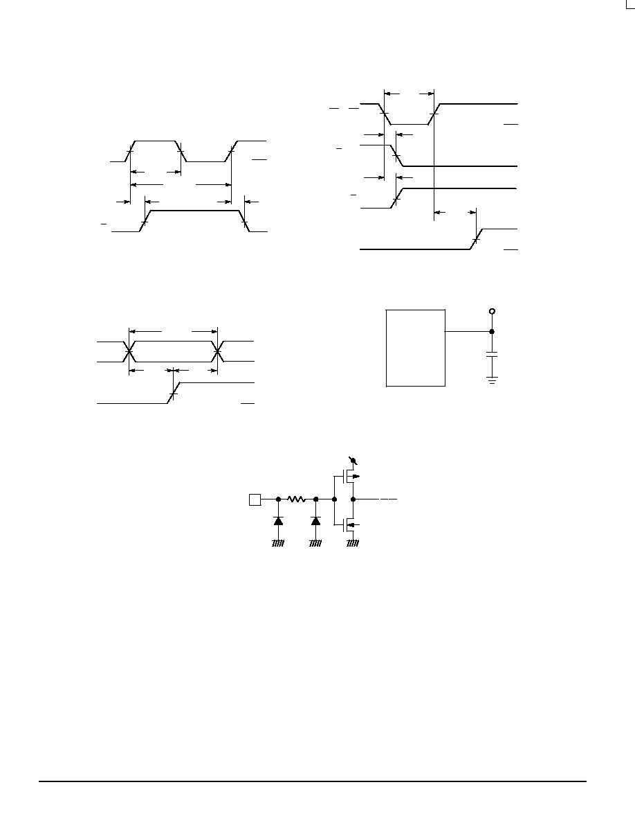
SWITCHING WAVEFORMS
Figure 1.
Figure 2.
50%
50% VCC
50% VCC
50%
VCC
VCC
GND
GND
SD or RD
Q or Q
Q or Q
CP
tPLH
tPHL
50%
D
CP
VCC
VCC
GND
Figure 3.
VALID
GND
tsu
th
trec
tw
* Includes all probe and jig capacitance
CL*
TEST POINT
DEVICE
UNDER
TEST
OUTPUT
Figure 4.
1/fmax
CP
Q or Q
VCC
GND
50%
50% VCC
tPLH
tPHL
tw
50%
Figure 5. Input Equivalent Circuit
INPUT
MC74VHC74
VHC Data ≠ Advanced CMOS Logic
DL203 -- Rev 1
5
MOTOROLA
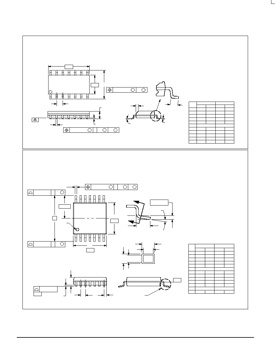
OUTLINE DIMENSIONS
D SUFFIX
PLASTIC SOIC PACKAGE
CASE 751A≠03
ISSUE F
MIN
MIN
MAX
MAX
MILLIMETERS
INCHES
DIM
A
B
C
D
F
G
J
K
M
P
R
8.55
3.80
1.35
0.35
0.40
0.19
0.10
0
∞
5.80
0.25
8.75
4.00
1.75
0.49
1.25
0.25
0.25
7
∞
6.20
0.50
0.337
0.150
0.054
0.014
0.016
0.008
0.004
0
∞
0.228
0.010
0.344
0.157
0.068
0.019
0.049
0.009
0.009
7
∞
0.244
0.019
1.27 BSC
0.050 BSC
NOTES:
1. DIMENSIONING AND TOLERANCING PER ANSI
Y14.5M, 1982.
2. CONTROLLING DIMENSION: MILLIMETER.
3. DIMENSIONS A AND B DO NOT INCLUDE
MOLD PROTRUSION.
4. MAXIMUM MOLD PROTRUSION 0.15 (0.006)
PER SIDE.
5. DIMENSION D DOES NOT INCLUDE DAMBAR
PROTRUSION. ALLOWABLE DAMBAR
PROTRUSION SHALL BE 0.127 (0.005) TOTAL
IN EXCESS OF THE D DIMENSION AT
MAXIMUM MATERIAL CONDITION.
≠A≠
≠B≠
P
7 PL
G
C
K
SEATING
PLANE
D
14 PL
M
J
R
X 45
∞
1
7
8
14
0.25 (0.010)
T
B
A
M
S
S
B
0.25 (0.010)
M
M
F
DT SUFFIX
PLASTIC TSSOP PACKAGE
CASE 948G≠01
ISSUE O
DIM
MIN
MAX
MIN
MAX
INCHES
MILLIMETERS
A
4.90
5.10
0.193
0.200
B
4.30
4.50
0.169
0.177
C
≠≠≠
1.20
≠≠≠
0.047
D
0.05
0.15
0.002
0.006
F
0.50
0.75
0.020
0.030
G
0.65 BSC
0.026 BSC
H
0.50
0.60
0.020
0.024
J
0.09
0.20
0.004
0.008
J1
0.09
0.16
0.004
0.006
K
0.19
0.30
0.007
0.012
K1
0.19
0.25
0.007
0.010
L
6.40 BSC
0.252 BSC
M
0
8
0
8
NOTES:
1. DIMENSIONING AND TOLERANCING PER ANSI
Y14.5M, 1982.
2. CONTROLLING DIMENSION: MILLIMETER.
3. DIMENSION A DOES NOT INCLUDE MOLD FLASH,
PROTRUSIONS OR GATE BURRS. MOLD FLASH
OR GATE BURRS SHALL NOT EXCEED 0.15
(0.006) PER SIDE.
4. DIMENSION B DOES NOT INCLUDE INTERLEAD
FLASH OR PROTRUSION. INTERLEAD FLASH OR
PROTRUSION SHALL NOT EXCEED
0.25 (0.010) PER SIDE.
5. DIMENSION K DOES NOT INCLUDE DAMBAR
PROTRUSION. ALLOWABLE DAMBAR
PROTRUSION SHALL BE 0.08 (0.003) TOTAL IN
EXCESS OF THE K DIMENSION AT MAXIMUM
MATERIAL CONDITION.
6. TERMINAL NUMBERS ARE SHOWN FOR
REFERENCE ONLY.
7. DIMENSION A AND B ARE TO BE DETERMINED
AT DATUM PLANE ≠W≠.
_
_
_
_
S
U
0.15 (0.006) T
2X
L/2
S
U
M
0.10 (0.004)
V
S
T
L
≠U≠
SEATING
PLANE
0.10 (0.004)
≠T≠
«««
«««
SECTION N≠N
DETAIL E
J J1
K
K1
………
………
DETAIL E
F
M
≠W≠
0.25 (0.010)
8
14
7
1
PIN 1
IDENT.
H
G
A
D
C
B
S
U
0.15 (0.006) T
≠V≠
14X REF
K
N
N
MC74VHC74
MOTOROLA
VHC Data ≠ Advanced CMOS Logic
DL203 -- Rev 1
6
OUTLINE DIMENSIONS
M SUFFIX
PLASTIC SOIC EIAJ PACKAGE
CASE 965≠01
ISSUE O
HE
A1
DIM
MIN
MAX
MIN
MAX
INCHES
≠≠≠
2.05
≠≠≠
0.081
MILLIMETERS
0.05
0.20
0.002
0.008
0.35
0.50
0.014
0.020
0.18
0.27
0.007
0.011
9.90
10.50
0.390
0.413
5.10
5.45
0.201
0.215
1.27 BSC
0.050 BSC
7.40
8.20
0.291
0.323
0.50
0.85
0.020
0.033
1.10
1.50
0.043
0.059
0
0.70
0.90
0.028
0.035
≠≠≠
1.42
≠≠≠
0.056
A1
HE
Q1
LE
_
10
_
0
_
10
_
LE
Q1
_
NOTES:
1. DIMENSIONING AND TOLERANCING PER ANSI
Y14.5M, 1982.
2. CONTROLLING DIMENSION: MILLIMETER.
3. DIMENSIONS D AND E DO NOT INCLUDE MOLD
FLASH OR PROTRUSIONS AND ARE MEASURED
AT THE PARTING LINE. MOLD FLASH OR
PROTRUSIONS SHALL NOT EXCEED 0.15 (0.006)
PER SIDE.
4. TERMINAL NUMBERS ARE SHOWN FOR
REFERENCE ONLY.
5. THE LEAD WIDTH DIMENSION (b) DOES NOT
INCLUDE DAMBAR PROTRUSION. ALLOWABLE
DAMBAR PROTRUSION SHALL BE 0.08 (0.003)
TOTAL IN EXCESS OF THE LEAD WIDTH
DIMENSION AT MAXIMUM MATERIAL CONDITION.
DAMBAR CANNOT BE LOCATED ON THE LOWER
RADIUS OR THE FOOT. MINIMUM SPACE
BETWEEN PROTRUSIONS AND ADJACENT LEAD
TO BE 0.46 ( 0.018).
0.13 (0.005)
M
0.10 (0.004)
D
Z
E
1
14
8
7
e
A
b
VIEW P
c
L
DETAIL P
M
A
b
c
D
E
e
0.50
M
Z
Motorola reserves the right to make changes without further notice to any products herein. Motorola makes no warranty, representation or guarantee regarding
the suitability of its products for any particular purpose, nor does Motorola assume any liability arising out of the application or use of any product or circuit, and
specifically disclaims any and all liability, including without limitation consequential or incidental damages. "Typical" parameters which may be provided in Motorola
data sheets and/or specifications can and do vary in different applications and actual performance may vary over time. All operating parameters, including "Typicals"
must be validated for each customer application by customer's technical experts. Motorola does not convey any license under its patent rights nor the rights of
others. Motorola products are not designed, intended, or authorized for use as components in systems intended for surgical implant into the body, or other
applications intended to support or sustain life, or for any other application in which the failure of the Motorola product could create a situation where personal injury
or death may occur. Should Buyer purchase or use Motorola products for any such unintended or unauthorized application, Buyer shall indemnify and hold Motorola
and its officers, employees, subsidiaries, affiliates, and distributors harmless against all claims, costs, damages, and expenses, and reasonable attorney fees
arising out of, directly or indirectly, any claim of personal injury or death associated with such unintended or unauthorized use, even if such claim alleges that
Motorola was negligent regarding the design or manufacture of the part. Motorola and are registered trademarks of Motorola, Inc. Motorola, Inc. is an Equal
Opportunity/Affirmative Action Employer.
Mfax is a trademark of Motorola, Inc.
How to reach us:
USA / EUROPE / Locations Not Listed: Motorola Literature Distribution;
JAPAN: Nippon Motorola Ltd.: SPD, Strategic Planning Office, 4≠32≠1,
P.O. Box 5405, Denver, Colorado 80217. 303≠675≠2140 or 1≠800≠441≠2447
Nishi≠Gotanda, Shinagawa≠ku, Tokyo 141, Japan. 81≠3≠5487≠8488
Mfax
TM
: RMFAX0@email.sps.mot.com ≠ TOUCHTONE 602≠244≠6609
ASIA/PACIFIC: Motorola Semiconductors H.K. Ltd.; 8B Tai Ping Industrial Park,
≠ US & Canada ONLY 1≠800≠774≠1848
51 Ting Kok Road, Tai Po, N.T., Hong Kong. 852≠26629298
INTERNET: http://motorola.com/sps
MC74VHC74/D