 | ÐлекÑÑоннÑй компоненÑ: 56F8346 | СкаÑаÑÑ:  PDF PDF  ZIP ZIP |
Äîêóìåíòàöèÿ è îïèñàíèÿ www.docs.chipfind.ru
MC56F8346/D
Rev. 8.0, 6/2004
© Motorola, Inc., 2004. All rights reserved.
56F8346
Preliminary Technical Data
56F8346 16-bit Hybrid Controller
· Up to 60 MIPS at 60MHz core frequency
· DSP and MCU functionality in a unified,
C-efficient architecture
· Access up to 1MB of off-chip program and data
memory
· Chip Select Logic for glueless interface to ROM
and SRAM
· 128KB of Program Flash
· 4KB of Program RAM
· 8KB of Data Flash
· 8KB of Data RAM
· 8KB of Boot Flash
· Two 6-channel PWM Modules
· Four 4-channel, 12-bit ADCs
· Temperature Sensor
· Two Quadrature Decoders
· Optional On-Chip Regulator
· FlexCAN module
· Two Serial Communication Interfaces (SCIs)
· Up to two Serial Peripheral Interfaces (SPIs)
· Up to four general-purpose Quad Timers
· Computer Operating Properly (COP) / Watchdog
· JTAG/Enhanced On-Chip Emulation (OnCETM) for
unobtrusive, real-time debugging
· Up to 62 GPIO lines
· 144-pin LQFP Package
56F8346 Block Diagram - 144 LQFP
Program Controller
and
Hardware Looping Unit
Data ALU
16 x 16 + 36 -> 36-Bit MAC
Three 16-bit Input Registers
Four 36-bit Accumulators
Address
Generation Unit
Bit
Manipulation
Unit
PLL
Clock
Generator
EXTAL
Interrupt
Controller
COP/
Watchdog
SCI1 or
GPIOD
4
External
Address Bus
Switch
E
x
ter
n
a
l Bu
s
In
t
e
r
f
ace
Un
i
t
2
CLKMODE
IRQA IRQB
External Data
Bus Switch
PDB
PDB
XAB1
XAB2
XDB2
CDBR
SCI0 or
GPIOE
SPI0 or
GPIOE
IPBus Bridge (IPBB)
Integration
Module
System
P
O
R
O
S
C
Decoding
Peripherals
Peripheral
Device Selects
RW
Control
IPAB
IPWDB
IPRDB
2
System Bus
R/W Control
PAB
PAB
CDBW
CDBR
CDBW
Clock
resets
JTAG/
EOnCE
Port
Digital Reg
Analog Reg
Low Voltage
Supervisor
V
CAP
V
DD
V
SS
V
DDA
V
SSA
5
4
7
5
2
V
PP
2
OCR_DIS
RESET
EXTBOOT
EMI_MODE
RSTO
4
3
6
PWM Outputs
Fault Inputs
PWMA
Current Sense Inputs
or GPIOC
3
4
6
PWM Outputs
Fault Inputs
PWMB
Current Sense Inputs
or GPIOD
3
Quad
Timer D or
GPIOE
Quad
Timer C or
GPIOE
AD0
AD1
ADCA
2
5
Quadrature
Decoder 0 or
Quad
Timer A or
GPIOC
FlexCAN
2
4
AD0
AD1
4
4
4
Temp_Sense
Quadrature
Decoder 1 or
Quad
Timer B or
SPI1 or
GPIOC
4
CLKO
Bus Control
6
2
8
7
9
2
XTAL
DS (CS1) or GPIOD9
PS (CS0) or GPIOD8
GPIOD0-1 or CS2-3
RD
WR
D7-15 or GPIOF0-8
D0-6 or GPIOF9-15
GPIOB0 or A16
A8-15 or GPIOA0-7
A0-5 or GPIOA8-13
A6-7 or GPIOE2-3
VREF
ADCB
16-Bit
56800E Core
Data Memory
4K x 16 Flash
4K x 16 RAM
Memory
Program Memory
64K x 16 Flash
2K x 16 RAM
4K x 16 Boot
Flash
Control
F
r
e
e
s
c
a
l
e
S
e
m
i
c
o
n
d
u
c
t
o
r
,
I
Freescale Semiconductor, Inc.
For More Information On This Product,
Go to: www.freescale.com
n
c
.
.
.

2
56F8346 Technical Data
Preliminary
Document Revision History
Version History
Description of Change
Rev 1.0
Pre-Release version, Alpha customers only
Rev 2.0
Initial Public Release
Rev 3.0
Corrected typo in
Table 10-4
, Flash Endurance is 10,000 cycles.
Additional grammar issues address
Rev 4.0
Added Package Pins to GPIO Table in
Part 8, General Purpose Input/Output (GPIO)
Added "Typical Min" values to
Table 10-17
Editing grammar, spelling, consistency of language throughout family
Updated values in Current Consumption per Power Supply Pin,
Table 10-7
,
Regulator Parameters
Table 10-9
,
External Clock Operation Timing Requirements
Table 10-13
,
SPI Timing
Table 10-18
,
ADC Parameters
Table 10-24
, and
IO Loading Coefficients at 10MHz
Table 10-25
.
Rev 5.0
Added
Section 4.8
,
added the word "access" to FM Error Interrupt in
Table 4-5
,
documenting only Typ. numbers for LVI in
Table 10-6
,
updated EMI numbers and writeup in
Section 10.9
.
Rev 6.0
Updated numbers in
Table 10-7
and
Table 10-8
with more recent data,
Corrected typo in
Table 10-3
in Pd characteristics.
Rev 7.0
Replace any reference to Flash Interface Unit with Flash Module, added note to Vcap pin
in
Table 2-2
, corrected thermal numbers for 144 LQFP in
Table 10-3
, removed
unneccessary notes in
Table 10-12
; corrected temperature range in
Table 10-14
; added
ADC calibration information to
Table 10-24
and new graphs in
Figure 10-22
.
Rev 8.0
Corrected EMI pin count in
Figure 1-1
, Clarification to
Table 10-23
, corrected Digital Input
Current Low (pull-up enabled) numbers in
Table 10-5
. Removed text and Table 10-2;
replaced with note to
Table 10-1
.
F
r
e
e
s
c
a
l
e
S
e
m
i
c
o
n
d
u
c
t
o
r
,
I
Freescale Semiconductor, Inc.
For More Information On This Product,
Go to: www.freescale.com
n
c
.
.
.

56F8346 Technical Data
3
Preliminary
Part 1: Overview . . . . . . . . . . . . . . . . . . . . 4
1.1. 56F8346 Features . . . . . . . . . . . . . . . . . . 4
1.2. 56F8346 Description . . . . . . . . . . . . . . . . 5
1.3. Award-Winning Development
Environment . . . . . . . . . . . . . . . 6
1.4. Architecture Block Diagram . . . . . . . . . . . 7
1.5. Product Documentation . . . . . . . . . . . . . 10
1.6. Data Sheet Conventions . . . . . . . . . . . . 11
Part 2: Signal/Connection Descriptions 12
2.1. Introduction . . . . . . . . . . . . . . . . . . . . . . 12
2.2. 56F8346 Signal Pins . . . . . . . . . . . . . . . 14
Part 3: On-Chip Clock Synthesis (OCCS) 31
3.1. Introduction . . . . . . . . . . . . . . . . . . . . . . 31
3.2. External Clock Operation . . . . . . . . . . . 32
3.3. Registers . . . . . . . . . . . . . . . . . . . . . . . . 33
Part 4: Memory Map . . . . . . . . . . . . . . . . 34
4.1. Introduction . . . . . . . . . . . . . . . . . . . . . . 34
4.2. Program Map . . . . . . . . . . . . . . . . . . . . 35
4.3. Interrupt Vector Table . . . . . . . . . . . . . . 36
4.4. Data Map . . . . . . . . . . . . . . . . . . . . . . . . 39
4.5. Flash Memory Map . . . . . . . . . . . . . . . . 40
4.6. EOnCE Memory Map . . . . . . . . . . . . . . 41
4.7. Peripheral Memory Mapped Registers . 41
4.8. Factory Programmed Memory . . . . . . . . 67
Part 5: Interrupt Controller (ITCN) . . . . . 68
5.1. Introduction . . . . . . . . . . . . . . . . . . . . . . 68
5.2. Features . . . . . . . . . . . . . . . . . . . . . . . . 68
5.3. Functional Description . . . . . . . . . . . . . . 68
5.4. Block Diagram . . . . . . . . . . . . . . . . . . . . 70
5.5. Operating Modes . . . . . . . . . . . . . . . . . . 70
5.6. Register Descriptions . . . . . . . . . . . . . . 71
5.7. Resets . . . . . . . . . . . . . . . . . . . . . . . . . . 96
Part 6: System Integration Module (SIM) 97
6.1. Overview . . . . . . . . . . . . . . . . . . . . . . . . 97
6.2. Features . . . . . . . . . . . . . . . . . . . . . . . . 97
6.3. Operating Modes . . . . . . . . . . . . . . . . . . 98
6.4. Operation Mode Register . . . . . . . . . . . 98
6.5. Register Descriptions . . . . . . . . . . . . . . 99
6.6. Clock Generation Overview . . . . . . . . 112
6.7. Power-Down Modes Overview . . . . . . 112
6.8. Stop and Wait Mode Disable Function 113
6.9. Resets . . . . . . . . . . . . . . . . . . . . . . . . . 113
Part 7: Security Features . . . . . . . . . . . 114
7.1. Operation with Security Enabled . . . . . 114
7.2. Flash Access Blocking Mechanisms . . 114
Part 8: General Purpose Input/Output
(GPIO) . . . . . . . . . . . . . . . . . . . . . 118
8.1. Introduction . . . . . . . . . . . . . . . . . . . . . 118
8.2. Configuration . . . . . . . . . . . . . . . . . . . . 118
8.3. Memory Maps 122
Part 9: Joint Test Action Group (JTAG) 122
9.1. 56F8346 Information . . . . . . . . . . . . . . 122
Part 10: Specifications . . . . . . . . . . . . . 123
10.1. General Characteristics . . . . . . . . . . . 123
10.2. DC Electrical Characteristics . . . . . . . 127
10.3. Temperature Sense . . . . . . . . . . . . . . 130
10.4. AC Electrical Characteristics . . . . . . . 130
10.5. Flash Memory Characteristics . . . . . . 131
10.6. External Clock Operation Timing . . . . 132
10.7. Phase Locked Loop Timing . . . . . . . . 132
10.8. Crystal Oscillator Timing . . . . . . . . . . 133
10.9. External Memory Interface Timing . . . 133
10.10. Reset, Stop, Wait, Mode Select,
and Interrupt Timing . . . . . . . 136
10.11. Serial Peripheral Interface (SPI)
Timing . . . . . . . . . . . . . . . . . . 138
10.12. Quad Timer Timing . . . . . . . . . . . . . 141
10.13. Quadrature Decoder Timing . . . . . . . 141
10.14. Serial Communication Interface
(SCI) Timing . . . . . . . . . . . . . 142
10.15. Controller Area Network (CAN)
Timing . . . . . . . . . . . . . . . . . . 143
10.16. JTAG Timing . . . . . . . . . . . . . . . . . . 143
10.17. Analog-to-Digital Converter (ADC)
Parameters . . . . . . . . . . . . . . 145
10.18. Equivalent Circuit for ADC Inputs . . . 147
10.19. Power Consumption . . . . . . . . . . . . . 147
Part 11: Packaging . . . . . . . . . . . . . . . . 149
11.1. Package and Pin-Out Information
56F8346 . . . . . . . . . . . . . . . . 149
Part 12: Design Considerations . . . . . . 153
12.1. Thermal Design Considerations . . . . . 153
12.2. Electrical Design Considerations . . . . 154
12.3. Power Distribution and I/O Ring
Implementation . . . . . . . . . . . 155
Part 13: Ordering Information . . . . . . . 156
56F8346 Data Sheet Table of Contents
Please see http://www.motorola.com/semiconductors for the most current Data Sheet revision.
F
r
e
e
s
c
a
l
e
S
e
m
i
c
o
n
d
u
c
t
o
r
,
I
Freescale Semiconductor, Inc.
For More Information On This Product,
Go to: www.freescale.com
n
c
.
.
.

4
56F8346 Technical Data
Preliminary
Part 1 Overview
1.1 56F8346 Features
1.1.1
Digital Signal Processing Core
·
Efficient 16-bit 56800E family hybrid controller engine with dual Harvard architecture
·
As many as 60 Million Instructions Per Second (MIPS) at 60MHz core frequency
·
Single-cycle 16
×
16-bit parallel Multiplier-Accumulator (MAC)
·
Four 36-bit accumulators, including extension bits
·
Arithmetic and logic multi-bit shifter
·
Parallel instruction set with unique DSP addressing modes
·
Hardware DO and REP loops
·
Three internal address buses
·
Four internal data buses
·
Instruction set supports both DSP and controller functions
·
Controller-style addressing modes and instructions for compact code
·
Efficient C compiler and local variable support
·
Software subroutine and interrupt stack with depth limited only by memory
·
JTAG/EOnCE debug programming interface
1.1.2
Memory
·
Harvard architecture permits as many as three simultaneous accesses to program and data memory
·
Flash security protection feature
·
On-chip memory, including a low-cost, high-volume Flash solution
-- 128KB of Program Flash
-- 4KB of Program RAM
-- 8KB of Data Flash
-- 8KB of Data RAM
-- 8KB of Boot Flash
·
Off-chip memory expansion capabilities programmable for 0 - 30 wait states
-- Access up to 1MB of program memory or 1MB of data memory
-- Chip select logic for glueless interface to ROM and SRAM
·
EEPROM emulation capability
1.1.3
Peripheral Circuits for 56F8346
·
Two Pulse Width Modulator modules each with six PWM outputs, three Current Sense inputs, and
three Fault inputs; fault-tolerant design with dead time insertion; supports both center-aligned and
edge-aligned modes
·
Four 12-bit, Analog-to-Digital Converters (ADCs), which support four simultaneous conversions
with quad, 4-pin multiplexed inputs; ADC and PWM modules can be synchronized through Timer
C, channels 2 and 3
·
Two four-input Quadrature Decoders or two additional Quad Timers
F
r
e
e
s
c
a
l
e
S
e
m
i
c
o
n
d
u
c
t
o
r
,
I
Freescale Semiconductor, Inc.
For More Information On This Product,
Go to: www.freescale.com
n
c
.
.
.

56F8346 Description
56F8346 Technical Data
5
Preliminary
·
Temperature Sensor diode can be connected, on the board, to any of the ADC inputs to monitor the
on-chip temperature
·
Four dedicated general-purpose Quad Timers totaling three dedicated pins: Timer C with one pin
and Timer D with two pins
·
Optional On-Chip Regulator
·
FlexCAN (CAN Version 2.0 B-compliant ) module with 2-pin port for transmit and receive
·
Two Serial Communication Interfaces (SCIs), each with two pins (or four additional GPIO lines)
·
Up to two Serial Peripheral Interfaces (SPIs), both with configurable 4-pin port (or eight additional
GPIO lines); SPI1 can also be used as Quadrature Decoder 1 or Quad Timer B
·
Computer Operating Properly (COP)/Watchdog timer
·
Two dedicated external interrupt pins
·
62 General Purpose I/O (GPIO) pins
·
External reset input pin for hardware reset
·
External reset output pin for system reset
·
Integrated low-voltage interrupt module
·
JTAG/Enhanced On-Chip Emulation (OnCE) for unobtrusive, processor speed-independent,
real-time debugging
·
Software-programmable, Phase Lock Loop (PLL)-based frequency synthesizer for the core clock
1.1.4
Energy Information
·
Fabricated in high-density CMOS with 5V-tolerant, TTL-compatible digital inputs
·
On-board 3.3V down to 2.6V voltage regulator for powering internal logic and memories; can be
disabled
·
On-chip regulators for digital and analog circuitry to lower cost and reduce noise
·
Wait and Stop modes available
·
ADC smart power management
·
Each peripheral can be individually disabled to save power
1.2 56F8346 Description
The 56F8346 is a member of the 56800E core-based family of hybrid controllers. It combines, on
a single chip, the processing power of a DSP and the functionality of a microcontroller with a
flexible set of peripherals to create an extremely cost-effective solution. Because of its low cost,
configuration flexibility, and compact program code, the 56F8346 is well-suited for many
applications. The 56F8346 includes many peripherals that are especially useful for motion control,
smart appliances, steppers, encoders, tachometers, limit switches, power supply and control,
automotive control, engine management, noise suppression, remote utility metering, industrial
control for power, lighting, and automation applications.
The 56800E core is based on a Harvard-style architecture consisting of three execution units
operating in parallel, allowing as many as six operations per instruction cycle. The MCU-style
programming model and optimized instruction set allow straightforward generation of efficient,
compact DSP and control code. The instruction set is also highly efficient for C/C++ Compilers to
enable rapid development of optimized control applications.
The 56F8346 supports program execution from either internal or external memories. Two data
operands can be accessed from the on-chip data RAM per instruction cycle. The 56F8346 also
F
r
e
e
s
c
a
l
e
S
e
m
i
c
o
n
d
u
c
t
o
r
,
I
Freescale Semiconductor, Inc.
For More Information On This Product,
Go to: www.freescale.com
n
c
.
.
.

6
56F8346 Technical Data
Preliminary
provides two external dedicated interrupt lines and up to 62 General Purpose Input/Output (GPIO)
lines, depending on peripheral configuration.
The 56F8346 hybrid controller includes 128KB of Program Flash and 8KB of Data Flash (each
programmable through the JTAG port) with 4KB of Program RAM and 8KB of Data RAM. It also
supports program execution from external memory.
A total of 8KB of Boot Flash is incorporated for easy customer-inclusion of field-programmable
software routines that can be used to program the main Program and Data Flash memory areas.
Both Program and Data Flash memories can be independently bulk erased or erased in pages.
Program Flash page erase size is 1KB. Boot and Data Flash page erase size is 512 bytes. The Boot
Flash memory can also be either bulk or page erased.
A key application-specific feature of the 56F8346 is the inclusion of two Pulse Width Modulator
(PWM) modules. These modules each incorporate three complementary, individually
programmable PWM signal output pairs (each module is also capable of supporting six
independent PWM functions, for a total of 12 PWM outputs) to enhance motor control
functionality. Complementary operation permits programmable dead time insertion, distortion
correction via current sensing by software, and separate top and bottom output polarity control. The
up-counter value is programmable to support a continuously variable PWM frequency.
Edge-aligned and center-aligned synchronous pulse width control (0% to 100% modulation) is
supported. The device is capable of controlling most motor types: ACIM (AC Induction Motors);
both BDC and BLDC (Brush and Brushless DC motors); SRM and VRM (Switched and Variable
Reluctance Motors); and stepper motors. The PWMs incorporate fault protection and
cycle-by-cycle current limiting with sufficient output drive capability to directly drive standard
optoisolators. A "smoke-inhibit", write-once protection feature for key parameters is also included.
A patented PWM waveform distortion correction circuit is also provided. Each PWM is
double-buffered and includes interrupt controls to permit integral reload rates to be programmable
from 1 to 16. The PWM modules provide reference outputs to synchronize the Analog-to-Digital
Converters through two channels of Quad Timer C.
The 56F8346 incorporates two Quadrature Decoders capable of capturing all four transitions on
the two-phase inputs, permitting generation of a number proportional to actual position. Speed
computation capabilities accommodate both fast- and slow-moving shafts. An integrated watchdog
timer in the Quadrature Decoder can be programmed with a time-out value to alert when no shaft
motion is detected. Each input is filtered to ensure only true transitions are recorded.
This hybrid controller also provides a full set of standard programmable peripherals that include
two Serial Communications Interfaces (SCIs); two Serial Peripheral Interfaces (SPIs); and four
Quad Timers. Any of these interfaces can be used as General Purpose Input/Outputs (GPIOs) if
that function is not required. A Flex Controller Area Network (FlexCAN) interface (CAN Version
2.0 B-compliant) and an internal interrupt controller are a part of the 56F8346.
1.3 Award-Winning Development Environment
Processor Expert
TM
(PE) provides a Rapid Application Design (RAD) tool that combines
easy-to-use component-based software application creation with an expert knowledge system.
The CodeWarrior Integrated Development Environment is a sophisticated tool for code navigation,
compiling, and debugging. A complete set of evaluation modules (EVMs) and development
system cards will support concurrent engineering. Together, PE, CodeWarrior and EVMs create a
complete, scalable tools solution for easy, fast, and efficient development.
F
r
e
e
s
c
a
l
e
S
e
m
i
c
o
n
d
u
c
t
o
r
,
I
Freescale Semiconductor, Inc.
For More Information On This Product,
Go to: www.freescale.com
n
c
.
.
.

Architecture Block Diagram
56F8346 Technical Data
7
Preliminary
1.4 Architecture Block Diagram
The 56F8346 architecture is shown in
Figure 1-1
and
Figure 1-2
.
Figure 1-1
illustrates how the
56800E system buses communicate with internal memories, the external memory interface and the
IPBus Bridge.
Table 1-1
lists the internal buses in the 56800E architecture and provides a brief
description of their function.
Figure 1-2
shows the peripherals and control blocks connected to the
IPBus Bridge. The figures do not show the on-board regulator and power and ground signals. They
also do not show the multiplexing between peripherals or the dedicated GPIOs. Please see
Part 2,
Signal/Connection Descriptions,
to see which signals are multiplexed with those of other
peripherals.
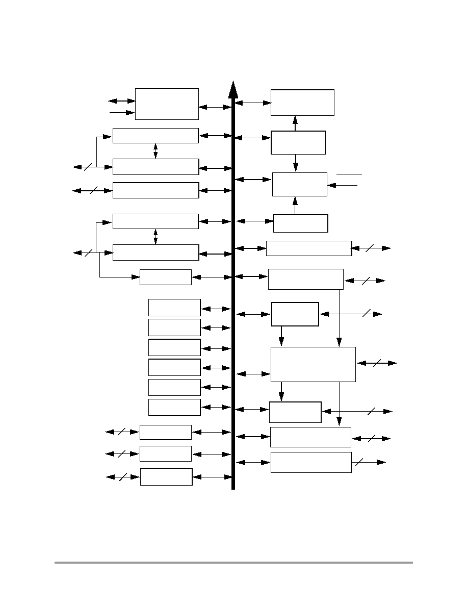
Also shown in
Figure 1-2
are connections between the PWM, Timer C and ADC blocks. These
connections allow the PWM and/or Timer C to control the timing of the start of ADC conversions.
The Timer C channel indicated can generate periodic start (SYNC) signals to the ADC to start its
conversions. In another operating mode, the PWM load interrupt (SYNC output) signal is routed
internally to the Timer C input channel as indicated. The timer can then be used to introduce a
controllable delay before generating its output signal. The timer output then triggers the ADC. To
fully understand this interaction, please see the 56F8300 Peripheral User Manual for clarification
on the operation of all three of these peripherals.
F
r
e
e
s
c
a
l
e
S
e
m
i
c
o
n
d
u
c
t
o
r
,
I
Freescale Semiconductor, Inc.
For More Information On This Product,
Go to: www.freescale.com
n
c
.
.
.
8
56F8346 Technical Data
Preliminary
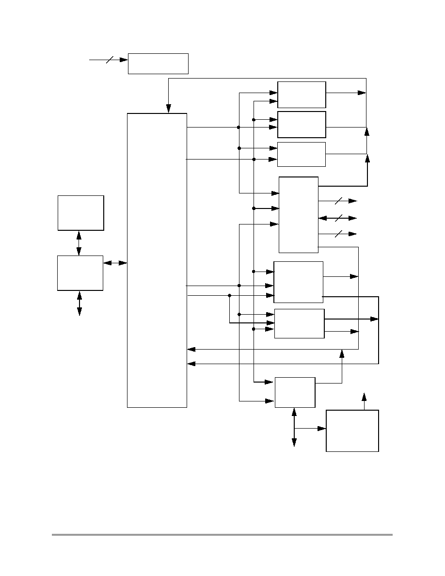
Figure 1-1 System Bus Interfaces
Note:
Flash memories are encapsulated within the Flash Interface Unit (FIU). Flash control is
accomplished by the I/O to the FIU over the peripheral bus, while reads and writes are
completed between the core and the Flash memories.
Note:
The primary data RAM port is 32 bits wide. Other data ports are16 bits.
56800E
Program
Flash
Program
RAM
Data RAM
pab[20:0]
xab1[23:0]
xab2[23:0]
EMI
17
16
6
Data Flash
pdb_m[15:0]
cdbw[31:0]
cdbr_m[31:0]
xdb2_m[15:0]
Address
Data
Control
IPBus
Bridge
IPBus
JTAG / EOnCE
5
Boot
Flash
Flash
Interface
Units
To Flash
Control Logic
CHIP
TAP
Controller
TAP
Linking
Module
External JTAG
Port
F
r
e
e
s
c
a
l
e
S
e
m
i
c
o
n
d
u
c
t
o
r
,
I
Freescale Semiconductor, Inc.
For More Information On This Product,
Go to: www.freescale.com
n
c
.
.
.
Architecture Block Diagram
56F8346 Technical Data
9
Preliminary
Figure 1-2 Peripheral Subsystem
IPBus
Timer A
Timer C
Timer D
SPI 1
ADCB
ADCA
1
2
8
8
FlexCAN
GPIOA
2
SPI0
SCI0
4
2
SCI1
Interrupt
Controller
To/From IPBus Bridge
PWMA
PWMB
12
13
ch3i ch2i
ch3o ch2o
System POR
Low Voltage Interrupt
COP Reset
COP
RESET
2
Quadrature Decoder 0
4
Note: ADCA and ADCB use the same
voltage reference circuit with V
REFH
,
V
REFP,
V
REFMID
, V
REFN
, and V
REFLO
pins.
GPIOB
GPIOC
GPIOD
GPIOE
GPIOF
Timer B
Quadrature Decoder 1
4
TEMP_SENSE
1
CLKGEN
(OSC/PLL)
POR & LVI
SIM
SYNC Output
SYNC Output
F
r
e
e
s
c
a
l
e
S
e
m
i
c
o
n
d
u
c
t
o
r
,
I
Freescale Semiconductor, Inc.
For More Information On This Product,
Go to: www.freescale.com
n
c
.
.
.

10
56F8346 Technical Data
Preliminary
1.5 Product Documentation
The documents in
Table 1-2
are required for a complete description and proper design with the
56F8346. Documentation is available from local Motorola distributors, Motorola semiconductor
sales offices, Motorola Literature Distribution Centers, or online at
http://www.motorola.com/semiconductors.
Table 1-2 56F8346 Chip Documentation
Table 1-1 Bus Signal Names
Name
Function
Program Memory Interface
pdb_m[15:0]
Program data bus for instruction word fetches or read operations.
cdbw[15:0]
Primary core data bus used for program memory writes. (Only these 16 bits of the cdbw[31:0] bus
are used for writes to program memory.)
pab[20:0]
Program memory address bus. Data is returned on pdb_m bus.
Primary Data Memory Interface Bus
cdbr_m[31:0]
Primary core data bus for memory reads. Addressed via xab1 bus.
cdbw[31:0]
Primary core data bus for memory writes. Addressed via xab1 bus.
xab1[23:0]
Primary data address bus. Capable of addressing bytes
1
, words, and long data types. Data is written
on cdbw and returned on cdbr_m. Also used to access memory-mapped I/O.
1.
Byte accesses can only occur in the bottom half of the memory address space. The MSB of the address will be forced to 0.
Secondary Data Memory Interface
xdb2_m[15:0] Secondary data bus used for secondary data address bus xab2 in the dual memory reads.
xab2[23:0]
Secondary data address bus used for the second of two simultaneous accesses. Capable of
addressing only words. Data is returned on xdb2_m.
Peripheral Interface Bus
IPBus [15:0]
Peripheral bus accesses all on-chip peripherals registers. This bus operates at the same clock rate
as the Primary Data Memory and therefore generates no delays when accessing the processor.
Write data is obtained from cdbw. Read data is provided to cdbr_m.
Topic
Description
Order Number
DSP56800E
Reference Manual
Detailed description of the 56800E family architecture,
and 16-bit hybrid controller core processor and the
instruction set
DSP56800ERM/D
568300 Peripheral User
Manual
Detailed description of peripherals of the 56F8300
devices
MC56F8300UM/D
56F8300 SCI/CAN
Bootloader User Manual
Detailed description of the SCI/CAN Bootloaders
56F8300 family of devices
MC56F83xxBLUM/D
56F8346
Technical Data Sheet
Electrical and timing specifications, pin descriptions,
and package descriptions (this document)
MC56F8346/D
56F8346
Product Brief
Summary description and block diagram of the
56F8346 core, memory, peripherals and interfaces
MC56F8346PB/D
56F8346
Errata
Details any chip issues that might be present
MC56F8346E/D
F
r
e
e
s
c
a
l
e
S
e
m
i
c
o
n
d
u
c
t
o
r
,
I
Freescale Semiconductor, Inc.
For More Information On This Product,
Go to: www.freescale.com
n
c
.
.
.

Data Sheet Conventions
56F8346 Technical Data
11
Preliminary
1.6 Data Sheet Conventions
This data sheet uses the following conventions:
OVERBAR
This is used to indicate a signal that is active when pulled low. For example, the RESET pin is
active when low.
"asserted"
A high true (active high) signal is high or a low true (active low) signal is low.
"deasserted"
A high true (active high) signal is low or a low true (active low) signal is high.
Examples:
Signal/Symbol
Logic State
Signal State
Voltage
1
1.
Values for VIL, VOL, VIH, and VOH are defined by individual product specifications.
PIN
True
Asserted
V
IL
/V
OL
PIN
False
Deasserted
V
IH
/V
OH
PIN
True
Asserted
V
IH
/V
OH
PIN
False
Deasserted
V
IL
/V
OL
F
r
e
e
s
c
a
l
e
S
e
m
i
c
o
n
d
u
c
t
o
r
,
I
Freescale Semiconductor, Inc.
For More Information On This Product,
Go to: www.freescale.com
n
c
.
.
.

12
56F8346 Technical Data
Preliminary
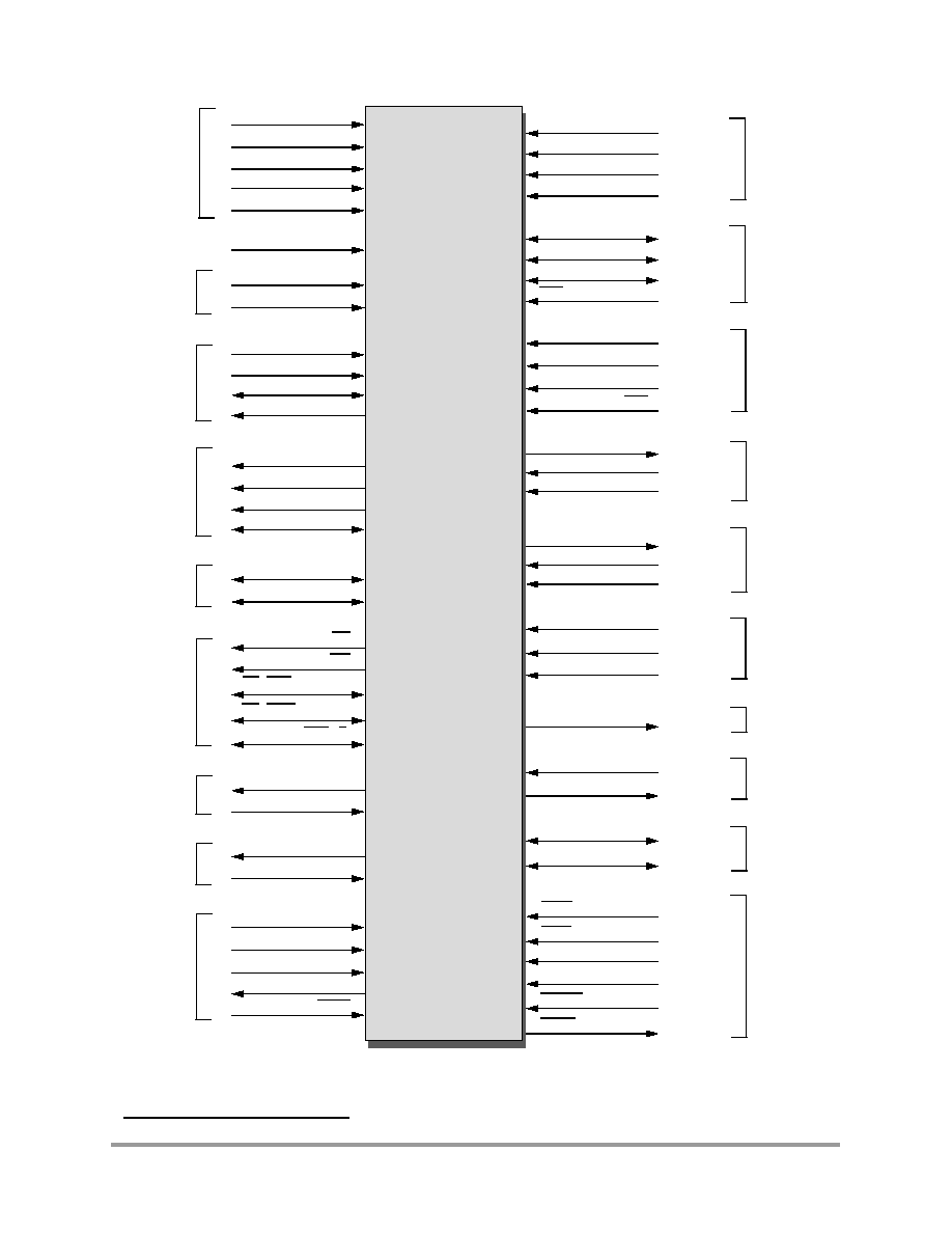
Part 2 Signal/Connection Descriptions
2.1 Introduction
The input and output signals of the 56F8346 are organized into functional groups, as detailed in
Table 2-1
and as illustrated in
Figure 2-1
. In
Table 2-2
, each table row describes the signal or
signals present on a pin.
Table 2-1 Functional Group Pin Allocations
Functional Group
Number of Pins
Power (V
DD
or V
DDA
)
9
Power Option Control
1
Ground (V
SS
or V
SSA
)
6
Supply Capacitors
1
& V
PP
1.
If the on-chip regulator is disabled, the V
CAP
pins serve as 2.5V V
DD_CORE
power inputs
6
PLL and Clock
4
Address Bus
17
Data Bus
16
Bus Control
6
Interrupt and Program Control
6
Pulse Width Modulator (PWM) Ports
25
Serial Peripheral Interface (SPI) Port 0
4
Quadrature Decoder Port 0
2
2.
Alternately, can function as Quad Timer pins or GPIO
4
Quadrature Decoder Port 1
3
3.
Pins in this section can function as Quad Timer, SPI #1, or GPIO
4
Serial Communications Interface (SCI) Ports
4
CAN Ports
2
Analog to Digital Converter (ADC) Ports
21
Timer Module Ports
3
JTAG/Enhanced On-Chip Emulation (EOnCE)
5
Temperature Sense
1
F
r
e
e
s
c
a
l
e
S
e
m
i
c
o
n
d
u
c
t
o
r
,
I
Freescale Semiconductor, Inc.
For More Information On This Product,
Go to: www.freescale.com
n
c
.
.
.
Introduction
56F8346 Technical Data
13
Preliminary
Figure 2-1 56F8346 Signals Identified by Functional Group
1
(144-pin LQFP)
1. Alternate pin functionality is shown in parenthesis; pin direction/type shown is the default functionality.
V
DD_IO
V
DDA_ADC
V
SS
V
SSA_ADC
Other
Supply
Ports
PLL
and
Clock
External
Address
Bus
or GPIO
External
Data Bus
or GPIO
SCI 0 or
GPIO
SCI 1
or GPIO
1
7
1
5
V
PP
1 & V
PP
2
2
Power
Ground
Power
Ground
A8 - A15 (GPIOA0 - 7)
TXD0 (GPIOE0)
RXD0 (GPIOE1)
TXD1 (GPIOD6)
RXD1 (GPIOD7)
TCK
TMS
TDI
TDO
TRST
Quadrature
Decoder 0
or Quad
Timer A or
GPIO
PHASEA0 (TA0, GPIOC4)
PHASEB0 (TA1, GPIOC5)
INDEX0 (TA2, GPIOC6)
HOME0 (TA3, GPIOC7)
PHASEB1 (TB1, MOSI1, GPIOC1)
INDEX1 (TB2, MISO1, GPIOC2)
HOME1 (TB3, SS1, GPIOC3)
PWMA0 - 5
ISA0 - 2 (GPIOC8 - 10)
FAULTA0 - 2
ISB0 - 2 (GPIOD10 - 12)
FAULTB0 - 3
PWMB0 - 5
ANA0 - 7
ANB0 - 7
V
REF
CAN_RX
CAN_TX
TC0 (GPIOE8)
TD0 - 1 (GPIOE10 - 11)
IRQA
IRQB
RESET
RSTO
SPI0 or
GPIO
PWMA or
GPIO
Quadrature
Decoder 1 or
Quad Timer B
or SPI 1 or
GPIO
PWMB or
GPIO
ADCB
ADCA
FlexCAN
QUAD TIMER
C and D or
GPIO
INTERRUPT/
PROGRAM
CONTROL
PHASEA1(TB0, SCLK1, GPIOC0)
8
1
GPIOB0 (A16)
1
1
1
1
1
1
1
1
1
1
1
1
1
1
1
1
1
6
3
3
6
3
4
8
5
8
1
1
1
1
2
1
1
1
1
1
56F8346
TEMP_SENSE
EXTAL
XTAL
CLKO
1
1
1
V
CAP
1 - V
CAP
4
4
A0 - A5 (GPIOA8 - 13)
6
A6 - A7 (GPIOE2 - 3)
2
RD
1
WR
1
PS (CS0)(GPIOD8)
1
DS (CS1)(GPIOD9)
1
GPIOD0 - 1 (CS2 - 3)
2
JTAG/
EOnCE
Port
External
Bus
Control or
GPIO
D7 - D15 (GPIOF0 - 8)
9
D0-D6 (GPIOF9 - 15)
7
EXTBOOT
MOSI0 (GPIOE5)
MISO0 (GPIOE6)
SS0 (GPIOE7)
1
1
1
SCLK0 (GPIOE4)
1
1
EMI_MODE
OCR_DIS
1
Power
CLKMODE
1
V
DDA_OSC_PLL
1
Temperature
Sensor
F
r
e
e
s
c
a
l
e
S
e
m
i
c
o
n
d
u
c
t
o
r
,
I
Freescale Semiconductor, Inc.
For More Information On This Product,
Go to: www.freescale.com
n
c
.
.
.

14
56F8346 Technical Data
Preliminary
2.2 56F8346 Signal Pins
After reset, each pin is configured for its primary function (listed first). Any alternate functionality
must be programmed.
If the "State During Reset" lists more than one state for a pin, the first state is the actual reset state.
Other states show the reset condition of the alternate function, which you get if the alternate pin
function is selected without changing the configuration of the alternate peripheral. For example,
the A8/GPIOA0 pin shows that it is tri-stated during reset. If the GPIOA_PER is changed to select
the GPIO function of the pin, it will become an input if no other registers are changed.
Table 2-2 56F8346 Signal and Package Information for the 144 Pin LQFP
Signal Name
Pin No.
Type
State
During
Reset
Signal Description
V
DD_IO
1
Supply
I/O Power -- This pin supplies 3.3V power to the chip I/O
interface.
V
DD_IO
16
V
DD_IO
31
V
DD_IO
38
V
DD_IO
66
V
DD_IO
84
V
DD_IO
119
V
DDA_ADC
102
Supply
ADC Power -- This pin supplies 3.3V power to the ADC
modules. It must be connected to a clean analog power
supply.
V
DDA_OSC_PLL
80
Supply
Oscillator and PLL Power -- This pin supplies 3.3V
power to the OSC and to the internal regulator that in turn
supplies the Phase Locked Loop. It must be connected to
a clean analog power supply.
V
SS
27
Supply
V
SS
-- These pins provide ground for chip logic and I/O
drivers.
V
SS
37
V
SS
63
V
SS
69
V
SS
144
V
SSA_ADC
103
Supply
ADC Analog Ground -- This pin supplies an analog
ground to the ADC modules.
OCR_DIS
79
Input
Input
On-Chip Regulator Disable --
Tie this pin to V
SS
to enable the on-chip regulator
Tie this pin to V
DD
to disable the on-chip regulator
This pin is intended to be a static DC signal from
power-up to shut down. Do not try to toggle this pin
for power savings during operation.
F
r
e
e
s
c
a
l
e
S
e
m
i
c
o
n
d
u
c
t
o
r
,
I
Freescale Semiconductor, Inc.
For More Information On This Product,
Go to: www.freescale.com
n
c
.
.
.

56F8346 Signal Pins
56F8346 Technical Data
15
Preliminary
V
CAP
1
51
Supply
Supply
V
CAP
1 - 4 -- When OCR_DIS is tied to V
SS
(regulator
enabled), connect each pin to a 2.2
µ
F or greater bypass
capacitor in order to bypass the core logic voltage
regulator, required for proper chip operation. When
OCR_DIS is tied to V
DD
(regulator disabled), these pins
become V
DD_CORE
and should be connected to a
regulated 2.5V power supply.
Note: This bypass is required even if the chip is
powered with an external supply.
V
CAP
2
128
V
CAP
3
83
V
CAP
4
15
V
PP
1
125
Input
Input
V
PP
1 - 2 -- These pins should be left unconnected as an
open circuit for normal functionality.
V
PP
2
2
CLKMODE
87
Input
Input
Clock Input Mode Selection -- This input determines the
function of the XTAL and EXTAL pins.
1 = External clock input on XTAL is used to directly drive
the input clock of the chip. The EXTAL pin should be
grounded.
0 = A crystal or ceramic resonator should be connected
between XTAL and EXTAL.
EXTAL
82
Input
Input
External Crystal Oscillator Input -- This input can be
connected to an 8MHz external crystal. Tie this pin low if
XTAL is driven by an external clock source.
XTAL
81
Input/
Output
Chip-driven
Crystal Oscillator Output -- This output connects the
internal crystal oscillator output to an external crystal.
If an external clock is used, XTAL must be used as the
input and EXTAL connected to GND.
The input clock can be selected to provide the clock
directly to the core. This input clock can also be selected
as the input clock for the on-chip PLL.
CLKO
3
Output
Tri-Stated
Clock Output -- This pin outputs a buffered clock signal.
Using the SIM CLKO Select Register (SIM_CLKOSR), this
pin can be programmed as any of the following: disabled,
CLK_MSTR (system clock), IPBus clock, oscillator output,
prescaler clock and postscaler clock. Other signals are
also available for test purposes.
See
Section 6.5.7
for details.
Table 2-2 56F8346 Signal and Package Information for the 144 Pin LQFP
Signal Name
Pin No.
Type
State
During
Reset
Signal Description
F
r
e
e
s
c
a
l
e
S
e
m
i
c
o
n
d
u
c
t
o
r
,
I
Freescale Semiconductor, Inc.
For More Information On This Product,
Go to: www.freescale.com
n
c
.
.
.

16
56F8346 Technical Data
Preliminary
A0
(GPIOA8)
138
Output
Input/
Output
Tri-stated
Input
Address Bus -- A0 - A5 specify six of the address lines
for external program or data memory accesses. Depending
upon the state of the DRV bit in the EMI bus control register
(BCR), A0 - A5 and EMI control signals are tri-stated when
the external bus is inactive.
Port A GPIO -- These six GPIO pins can be individually
programmed as input or output pins.
After reset, these pins default to address bus functionality
and must be programmed as GPIO.
To deactivate the internal pull-up resistor, clear the
appropriate GPIO bit in the GPIOA_PUR register.
Example: GPIOA8, clear bit 8 in the GPIOA_PUR register.
A1
(GPIOA9)
10
A2
(GPIOA10)
11
A3
(GPIOA11)
12
A4
(GPIOA12)
13
A5
(GPIOA13)
14
A6
(GPIOE2)
17
Output
Schmitt
Input/
Output
Tri-stated
Input
Address Bus -- A6 - A7 specify two of the address lines
for external program or data memory accesses. Depending
upon the state of the DRV bit in the EMI bus control register
(BCR), A6 - A7 and EMI control signals are tri-stated when
the external bus is inactive.
Port E GPIO -- These two GPIO pins can be individually
programmed as input or output pins.
After reset, the default state is Address Bus.
To deactivate the internal pull-up resistor, clear the
appropriate GPIO bit in the GPIOE_PUR register.
Example: GPIOE2, clear bit 2 in the GPIOE_PUR register.
A7
(GPIOE3)
18
Table 2-2 56F8346 Signal and Package Information for the 144 Pin LQFP
Signal Name
Pin No.
Type
State
During
Reset
Signal Description
F
r
e
e
s
c
a
l
e
S
e
m
i
c
o
n
d
u
c
t
o
r
,
I
Freescale Semiconductor, Inc.
For More Information On This Product,
Go to: www.freescale.com
n
c
.
.
.

56F8346 Signal Pins
56F8346 Technical Data
17
Preliminary
A8
(GPIOA0)
19
Output
Schmitt
Input/
Output
Tri-stated
Input
Address Bus-- A8 - A15 specify eight of the address lines
for external program or data memory accesses. Depending
upon the state of the DRV bit in the EMI bus control register
(BCR), A8 - A15 and EMI control signals are tri-stated when
the external bus is inactive.
Port A GPIO -- These eight GPIO pins can be individually
programmed as input or output pins.
After reset, the default state is Address Bus.
To deactivate the internal pull-up resistor, clear the
appropriate GPIO bit in the GPIOA_PUR register.
Example: GPIOA0, clear bit 0 in the GPIOA_PUR register.
A9
(GPIOA1)
20
A10
(GPIOA2)
21
A11
(GPIOA3)
22
A12
(GPIOA4)
23
A13
(GPIOA5)
24
A14
(GPIOA6)
25
A15
(GPIOA7)
26
GPIOB0
(A16)
33
Schmitt
Input/
Output
Output
Input
Tri-stated
Port B GPIO -- This GPIO pin can be programmed as an
input or output pin.
Address Bus -- A16 specifies one of the address lines for
external program or data memory accesses. Depending
upon the state of the DRV bit in the EMI bus control register
(BCR), A16 and EMI control signals are tri-stated when the
external bus is inactive.
After reset, the start-up state of GPIOB0 (GPIO or
address) is determined as a function of EXTBOOT,
EMI_MODE and the Flash security setting. See
Table 4-4
for further information on when this pin is configured as an
address pin at reset. In all cases, this state may be
changed by writing to GPIOB_PER.
To deactivate the internal pull-up resistor, clear bit 0 in the
GPIOB_PUR register.
Table 2-2 56F8346 Signal and Package Information for the 144 Pin LQFP
Signal Name
Pin No.
Type
State
During
Reset
Signal Description
F
r
e
e
s
c
a
l
e
S
e
m
i
c
o
n
d
u
c
t
o
r
,
I
Freescale Semiconductor, Inc.
For More Information On This Product,
Go to: www.freescale.com
n
c
.
.
.

18
56F8346 Technical Data
Preliminary
D0
(GPIOF9)
59
Input/
Outpu
Input/
Outputt
Tri-stated
Input
Data Bus -- D0 - D6 specify part of the data for external
program or data memory accesses.
Depending upon the state of the DRV bit in the EMI bus
control register (BCR), D0-D6 are tri-stated when the
external bus is inactive.
Port F GPIO -- These seven GPIO pins can be
individually programmed as input or output pins.
At reset, these pins default to the EMI data bus function.
To deactivate the internal pull-up resistor, clear the
appropriate GPIO bit in the GPIOF_PUR register.
Example: GPIOF9, clear bit 9 in the GPIOF_PUR register.
D1
(GPIOF10)
60
D2
(GPIOF11)
72
D3
(GPIOF12)
75
D4
(GPIOF13)
76
D5
(GPIOF14)
77
D6
(GPIOF15)
78
D7
(GPIOF0)
28
Input/
Output
Input/
Output
Tri-stated
Input
Data Bus -- D7 - D14 specify part of the data for external
program or data memory accesses.
Port F GPIO -- These eight GPIO pins can be individually
programmed as input or output pins.
At reset, these pins default to data bus functionality.
To deactivate the internal pull-up resistor, clear the
appropriate GPIO bit in the GPIOF_PUR register.
Example: GPIOF0, clear bit 0 in the GPIOF_PUR register.
D8
(GPIOF1)
29
D9
(GPIOF2)
30
D10
(GPIOF3)
32
D11
(GPIOF4)
133
D12
(GPIOF5)
134
D13
(GPIOF6)
135
D14
(GPIOF7)
136
Table 2-2 56F8346 Signal and Package Information for the 144 Pin LQFP
Signal Name
Pin No.
Type
State
During
Reset
Signal Description
F
r
e
e
s
c
a
l
e
S
e
m
i
c
o
n
d
u
c
t
o
r
,
I
Freescale Semiconductor, Inc.
For More Information On This Product,
Go to: www.freescale.com
n
c
.
.
.

56F8346 Signal Pins
56F8346 Technical Data
19
Preliminary
D15
(GPIOF8)
137
Input/
Output
Input/
Output
Tri-stated
Input
Data Bus -- D15 specifies part of the data for external
program or data memory accesses.
Port F GPIO -- This GPIO pin can be individually
programmed as an input or output pin.
At reset, this pin defaults to the data bus function.
To deactivate the internal pull-up resistor, clear bit 8 in the
GPIOF_PUR register.
RD
45
Output
Tri-stated
Read Enable -- RD is asserted during external memory
read cycles. When RD is asserted low, pins D0 - D15
become inputs and an external device is enabled onto the
data bus. When RD is deasserted high, the external data is
latched inside the device. When RD is asserted, it qualifies
the A0 - A16, PS, DS, and CSn
pins. RD can be connected
directly to the OE pin of a static RAM or ROM.
Depending upon the state of the DRV bit in the EMI bus
control register (BCR), RD is tri-stated when the external
bus is inactive.
To deactivate the internal pull-up resistor, set the CTRL bit
in the SIM_PUDR register.
WR
44
Output
Tri-stated
Write Enable -- WR is asserted during external memory
write cycles. When WR is asserted low, pins D0 - D15
become outputs and the device puts data on the bus.
When WR is deasserted high, the external data is latched
inside the external device. When WR is asserted, it
qualifies the A0 - A16, PS, DS, and CSn pins. WR can be
connected directly to the WE pin of a static RAM.
Depending upon the state of the DRV bit in the EMI bus
control register (BCR), WR
is tri-stated when the external
bus is inactive.
To deactivate the internal pull-up resistor, set the CTRL bit
in the SIM_PUDR register.
Table 2-2 56F8346 Signal and Package Information for the 144 Pin LQFP
Signal Name
Pin No.
Type
State
During
Reset
Signal Description
F
r
e
e
s
c
a
l
e
S
e
m
i
c
o
n
d
u
c
t
o
r
,
I
Freescale Semiconductor, Inc.
For More Information On This Product,
Go to: www.freescale.com
n
c
.
.
.
20
56F8346 Technical Data
Preliminary
PS
(CS0)
(GPIOD8)
46
Output
Input/
Output
Tri-stated
Input
Program Memory Select -- This signal is actually CS0 in
the EMI, which is programmed at reset for compatibility
with the 56F80x PS signal. PS is asserted low for external
program memory access.
Depending upon the state of the DRV bit in the EMI bus
control register (BCR),
PS is tri-stated when the external
bus is inactive.
Port D GPIO -- This GPIO pin can be individually
programmed as an input or output pin.
CS0 resets to provide the PS function as defined on the
56F80x devices.
To deactivate the internal pull-up resistor, clear bit 8 in the
GPIOD_PUR register.
DS
(CS1)
(GPIOD9)
47
Output
Input/
Output
Tri-stated
Input
Data Memory Select -- This signal is actually CS1 in the
EMI, which is programmed at reset for compatibility with
the 56F80x DS signal. DS is asserted low for external data
memory access.
Depending upon the state of the DRV bit in the EMI bus
control register (BCR), DS is tri-stated when the external
bus is inactive.
Port D GPIO -- This GPIO pin can be individually
programmed as an input or output pin.
CS1 resets to provide the DS function as defined on the
56F80x devices.
To deactivate the internal pull-up resistor, clear bit 9 in the
GPIOD_PUR register.
GPIOD0
(CS2)
48
Input/
Output
Output
Input
Tri-stated
Port D GPIO -- These two GPIO pins can be individually
programmed as input or output pins.
Chip Select -- CS2 - CS3 may be programmed within the
EMI module to act as chip selects for specific areas of the
external memory map.
Depending upon the state of the DRV bit in the EMI bus
control register (BCR), CS2 - CS3 are tri-stated when the
external bus is inactive.
At reset, these pins are configured as GPIO.
To deactivate the internal pull-up resistor, clear the
appropriate GPIO bit in the GPIOD_PUR register.
Example: GPIOD0, clear bit 0 in the GPIOD_PUR register.
GPIOD1
(CS3)
49
Table 2-2 56F8346 Signal and Package Information for the 144 Pin LQFP
Signal Name
Pin No.
Type
State
During
Reset
Signal Description
F
r
e
e
s
c
a
l
e
S
e
m
i
c
o
n
d
u
c
t
o
r
,
I
Freescale Semiconductor, Inc.
For More Information On This Product,
Go to: www.freescale.com
n
c
.
.
.

56F8346 Signal Pins
56F8346 Technical Data
21
Preliminary
TXD0
(GPIOE0)
4
Output
Input/
Output
Tri-stated
Input
Transmit Data -- SCI0 transmit data output
Port E GPIO -- This GPIO pin can be individually
programmed as an input or output pin.
After reset, the default state is SCI output.
To deactivate the internal pull-up resistor, clear bit 0 in the
GPIOE_PUR register.
RXD0
(GPIOE1)
5
Input
Input/
Output
Input
Input
Receive Data -- SCI0 receive data input
Port E GPIO -- This GPIO pin can be individually
programmed as an input or output pin.
After reset, the default state is SCI output.
To deactivate the internal pull-up resistor, clear bit 1 in the
GPIOE_PUR register.
TXD1
(GPIOD6)
42
Output
Input/
Output
Tri-stated
Input
Transmit Data -- SCI1 transmit data output
Port D GPIO -- This GPIO pin can be individually
programmed as an input or output pin.
After reset, the default state is SCI output.
To deactivate the internal pull-up resistor, clear bit 6 in the
GPIOD_PUR register.
RXD1
(GPIOD7)
43
Input
Input/
Output
Input
Input
Receive Data -- SCI1 receive data input
Port D GPIO -- This GPIO pin can be individually
programmed as an input or output pin.
After reset, the default state is SCI input.
To deactivate the internal pull-up resistor, clear bit 7 in the
GPIOD_PUR register.
TCK
121
Schmitt
Input
Input,
pulled low
internally
Test Clock Input -- This input pin provides a gated clock
to synchronize the test logic and shift serial data to the
JTAG/EOnCE port. The pin is connected internally to a
pull-down resistor.
TMS
122
Schmitt
Input
Input,
pulled high
internally
Test Mode Select Input -- This input pin is used to
sequence the JTAG TAP controller's state machine. It is
sampled on the rising edge of TCK and has an on-chip
pull-up resistor.
To deactivate the internal pull-up resistor, set the JTAG bit
in the SIM_PUDR register.
Table 2-2 56F8346 Signal and Package Information for the 144 Pin LQFP
Signal Name
Pin No.
Type
State
During
Reset
Signal Description
F
r
e
e
s
c
a
l
e
S
e
m
i
c
o
n
d
u
c
t
o
r
,
I
Freescale Semiconductor, Inc.
For More Information On This Product,
Go to: www.freescale.com
n
c
.
.
.

22
56F8346 Technical Data
Preliminary
TDI
123
Schmitt
Input
Input,
pulled high
internally
Test Data Input -- This input pin provides a serial input
data stream to the JTAG/EOnCE port. It is sampled on the
rising edge of TCK and has an on-chip pull-up resistor.
To deactivate the internal pull-up resistor, set the JTAG bit
in the SIM_PUDR register.
TDO
124
Output
Tri-stated
Test Data Output -- This tri-stateable output pin provides
a serial output data stream from the JTAG/EOnCE port. It
is driven in the shift-IR and shift-DR controller states, and
changes on the falling edge of TCK.
TRST
120
Schmitt
Input
Input,
pulled high
internally
Test Reset -- As an input, a low signal on this pin
provides a reset signal to the JTAG TAP controller. To
ensure complete hardware reset, TRST should be
asserted whenever RESET is asserted. The only
exception occurs in a debugging environment when a
hardware device reset is required and the JTAG/EOnCE
module must not be reset. In this case, assert RESET, but
do not assert TRST.
To deactivate the internal pull-up resistor, set the JTAG bit
in the SIM_PUDR register.
PHASEA0
(TA0)
(GPIOC4)
139
Schmitt
Input
Schmitt
Input/
Output
Schmitt
Input/
Output
Input
Input
Input
Phase A -- Quadrature Decoder 0, PHASEA input
TA0 -- Timer A, Channel 0
Port C GPIO -- This GPIO pin can be individually
programmed as an input or output pin.
After reset, the default state is PHASEA0.
To deactivate the internal pull-up resistor, clear bit 4 of the
GPIOC_PUR register.
PHASEB0
(TA1)
(GPIOC5)
140
Schmitt
Input
Schmitt
Input/
Output
Schmitt
Input/
Output
Input
Input
Input
Phase B -- Quadrature Decoder 0, PHASEB input
TA1 -- Timer A, Channel
Port C GPIO -- This GPIO pin can be individually
programmed as an input or output pin.
After reset, the default state is PHASEB0.
To deactivate the internal pull-up resistor, clear bit 5 of the
GPIOC_PUR register.
Table 2-2 56F8346 Signal and Package Information for the 144 Pin LQFP
Signal Name
Pin No.
Type
State
During
Reset
Signal Description
F
r
e
e
s
c
a
l
e
S
e
m
i
c
o
n
d
u
c
t
o
r
,
I
Freescale Semiconductor, Inc.
For More Information On This Product,
Go to: www.freescale.com
n
c
.
.
.

56F8346 Signal Pins
56F8346 Technical Data
23
Preliminary
INDEX0
(TA2)
(GPOPC6)
141
Schmitt
Input
Schmitt
Input/
Output
Schmitt
Input/
Output
Input
Input
Input
Index -- Quadrature Decoder 0, INDEX input
TA2 -- Timer A, Channel 2
Port C GPIO -- This GPIO pin can be individually
programmed as an input or output pin.
After reset, the default state is INDEX0.
To deactivate the internal pull-up resistor, clear bit 6 of the
GPIOC_PUR register.
HOME0
(TA3)
(GPIOC7)
142
Schmitt
Input
Schmitt
Input/
Output
Schmitt
Input/
Output
Input
Input
Input
Home -- Quadrature Decoder 0, HOME input
TA3 -- Timer A, Channel 3
Port C GPIO -- This GPIO pin can be individually
programmed as an input or output pin.
After reset, the default state is HOME0.
To deactivate the internal pull-up resistor, clear bit 7 of the
GPIOC_PUR register.
SCLK0
(GPIOE4)
130
Schmitt
Input/
Output
Schmitt
Input/
Output
Input
Input
SPI 0 Serial Clock -- In the master mode, this pin serves
as an output, clocking slaved listeners. In slave mode, this
pin serves as the data clock input.
Port E GPIO -- This GPIO pin can be individually
programmed as an input or output pin.
After reset, the default state is SCLK0.
To deactivate the internal pull-up resistor, clear bit 4 in the
GPIOE_PUR register.
MOSI0
(GPIOE5)
132
Input/
Output
Input/
Output
Tri-stated
Input
SPI 0 Master Out/Slave In -- This serial data pin is an
output from a master device and an input to a slave device.
The master device places data on the MOSI line a
half-cycle before the clock edge the slave device uses to
latch the data.
Port E GPIO -- This GPIO pin can be individually
programmed as an input or output pin.
After reset, the default state is MOSI0.
To deactivate the internal pull-up resistor, clear bit 5 in the
GPIOE_PUR register.
Table 2-2 56F8346 Signal and Package Information for the 144 Pin LQFP
Signal Name
Pin No.
Type
State
During
Reset
Signal Description
F
r
e
e
s
c
a
l
e
S
e
m
i
c
o
n
d
u
c
t
o
r
,
I
Freescale Semiconductor, Inc.
For More Information On This Product,
Go to: www.freescale.com
n
c
.
.
.

24
56F8346 Technical Data
Preliminary
MISO0
(GPIOE6)
131
Input/
Output
Input/
Output
Input
Input
SPI 0 Master In/Slave Out -- This serial data pin is an
input to a master device and an output from a slave device.
The MISO line of a slave device is placed in the
high-impedance state if the slave device is not selected.
The slave device places data on the MISO line a half-cycle
before the clock edge the master device uses to latch the
data.
Port E GPIO -- This GPIO pin can be individually
programmed as an input or output pin.
After reset, the default state is MISO0.
To deactivate the internal pull-up resistor, clear bit 6 in the
GPIOE_PUR register.
SS0
(GPIOE7)
129
Input
Input/
Output
Input
Input
SPI 0 Slave Select -- SS0 is used in slave mode to
indicate to the SPI module that the current transfer is to be
received.
Port E GPIO -- This GPIO pin can be individually
programmed as input or output pin.
After reset, the default state is SS0.
To deactivate the internal pull-up resistor, clear bit 7 in the
GPIOE_PUR register.
PHASEA1
(TB0)
(SCLK1)
(GPIOC0)
6
Schmitt
Input
Schmitt
Input/
Output
Schmitt
Input/
Output
Schmitt
Input/
Output
Input
Input
Input
Input
Phase A1 -- Quadrature Decoder, PHASEA input for
decoder 1.
TB0 -- Timer B, Channel 0
SPI 1 Serial Clock -- In the master mode, this pin serves
as an output, clocking slaved listeners. In slave mode, this
pin serves as the data clock input. To activate the SPI
function, set the PHSA_ALT bit in the SIM_GPS register.
For details, see
Section 6.5.8
.
Port C GPIO -- This GPIO pin can be individually
programmed as an input or output pin.
After reset, the default state is PHASEA1.
To deactivate the internal pull-up resistor, clear bit 0 in the
GPIOC_PUR register.
Table 2-2 56F8346 Signal and Package Information for the 144 Pin LQFP
Signal Name
Pin No.
Type
State
During
Reset
Signal Description
F
r
e
e
s
c
a
l
e
S
e
m
i
c
o
n
d
u
c
t
o
r
,
I
Freescale Semiconductor, Inc.
For More Information On This Product,
Go to: www.freescale.com
n
c
.
.
.

56F8346 Signal Pins
56F8346 Technical Data
25
Preliminary
PHASEB1
(TB1)
(MOSI1)
(GPIOC1)
7
Schmitt
Input
Schmitt
Input/
Output
Schmitt
Input/
Output
Schmitt
Input/
Output
Input
Input
Tri-stated
Input
Phase B1 -- Quadrature Decoder 1, PHASEB input for
decoder 1.
TB1 -- Timer B, Channel 1
SPI 1 Master Out/Slave In -- This serial data pin is an
output from a master device and an input to a slave device.
The master device places data on the MOSI line a
half-cycle before the clock edge the slave device uses to
latch the data. To activate the SPI function, set the
PHSB_ALT bit in the SIM_GPS register. For details, see
Section 6.5.8
.
Port C GPIO -- This GPIO pin can be individually
programmed as an input or output pin.
After reset, the default state is PHASEB1.
To deactivate the internal pull-up resistor, clear bit 1 in the
GPIOC_PUR register.
INDEX1
(TB2)
(MISO1)
(GPIOC2)
8
Schmitt
Input
Schmitt
Input/
Output
Schmitt
Input/
Output
Schmitt
Input/
Output
Input
Input
Input
Input
Index1 -- Quadrature Decoder 1, INDEX input
TB2 -- Timer B, Channel 2
SPI 1 Master In/Slave Out -- This serial data pin is an
input to a master device and an output from a slave device.
The MISO line of a slave device is placed in the
high-impedance state if the slave device is not selected.
The slave device places data on the MISO line a half-cycle
before the clock edge the master device uses to latch the
data. To activate the SPI function, set the INDEX_ALT bit
in the SIM_GPS register. For details, see
Section 6.5.8
.
Port C GPIO -- This GPIO pin can be individually
programmed as an input or output pin.
After reset, the default state is INDEX1.
To deactivate the internal pull-up resistor, clear bit 2 in the
GPIOC_PUR register.
Table 2-2 56F8346 Signal and Package Information for the 144 Pin LQFP
Signal Name
Pin No.
Type
State
During
Reset
Signal Description
F
r
e
e
s
c
a
l
e
S
e
m
i
c
o
n
d
u
c
t
o
r
,
I
Freescale Semiconductor, Inc.
For More Information On This Product,
Go to: www.freescale.com
n
c
.
.
.

26
56F8346 Technical Data
Preliminary
HOME1
(TB3)
(SS1)
(GPIOC3)
9
Schmitt
Input
Schmitt
Input/
Output
Schmitt
Input
Schmitt
Input/
Output
Input
Input
Input
Input
Home -- Quadrature Decoder 1, HOME input
TB3 -- Timer B, Channel 3
SPI 1 Slave Select -- In the master mode, this pin is used
to arbitrate multiple masters. In slave mode, this pin is
used to select the slave. To activate the SPI function, set
the HOME_ALT bit in the SIM_GPS register. For details,
see
Section 6.5.8
.
Port C GPIO -- This GPIO pin can be individually
programmed as an input or output pin.
After reset, the default state is HOME1.
To deactivate the internal pull-up resistor, clear bit 3 in the
GPIOC_PUR register.
PWMA0
62
Output
Tri-State
PWMA0 - 5 -- These are six PWMA outputs.
PWMA1
64
PWMA2
65
PWMA3
67
PWMA4
68
PWMA5
70
ISA0
(GPIOC8)
113
Schmitt
Input
Schmitt
Input/
Output
Input
Input
ISA0 - 2 -- These three input current status pins are used
for top/bottom pulse width correction in complementary
channel operation for PWMA.
Port C GPIO -- These three GPIO pins can be individually
programmed as input or output pins.
At reset, these pins default to ISA functionality.
To deactivate the internal pull-up resistor, clear the
appropriate bit of the GPIOC_PUR register. For details,
see
Section 6.5.8
.
ISA1
(GPIOC9)
114
ISA2
(GPIOC10)
115
FAULTA0
71
Schmitt
Input
Input
FAULTA0 - 2 -- These three fault input pins are used for
disabling selected PWMA outputs in cases where fault
conditions originate off-chip.
To deactivate the internal pull-up resistor, set the PWMA0
bit in the SIM_PUDR register. For details, see
Section
6.5.8
.
FAULTtA1
73
FAULTA2
74
Table 2-2 56F8346 Signal and Package Information for the 144 Pin LQFP
Signal Name
Pin No.
Type
State
During
Reset
Signal Description
F
r
e
e
s
c
a
l
e
S
e
m
i
c
o
n
d
u
c
t
o
r
,
I
Freescale Semiconductor, Inc.
For More Information On This Product,
Go to: www.freescale.com
n
c
.
.
.

56F8346 Signal Pins
56F8346 Technical Data
27
Preliminary
PWMB0
34
Output
Tri-State
PWMB0 - 5 -- Six PWMB output pins.
PWMB1
35
PWMB2
36
PWMB3
39
PWMB4
40
PWMB5
41
ISB0
(GPIOD10)
50
Schmitt
Input
Schmitt
Input/
Output
Input
Input
ISB0 - 2 -- These three input current status pins are used
for top/bottom pulse width correction in complementary
channel operation for PWMB.
Port D GPIO -- These three GPIO pins can be individually
programmed as input or output pins.
At reset, these pins default to ISB functionality.
To deactivate the internal pull-up resistor, clear the
appropriate bit of the GPIOD_PUR register. For details,
see
Section 6.5.8
.
ISB1
(GPIOD11)
52
ISB2
(GPIOD12)
53
FAULTB0
56
Schmitt
Input
Input
FAULTB0 - 3 -- These four fault input pins are used for
disabling selected PWMB outputs in cases where fault
conditions originate off-chip.
To deactivate the internal pull-up resistor, set the PWMB
bit in the SIM_PUDR register. For details, see
Section
6.5.8
.
FAULTB1
57
FAULTB2
58
FAULTB3
61
ANA0
88
Input
Input
ANA0 - 3 -- Analog inputs to ADC A, channel 0
ANA1
89
ANA2
90
ANA3
91
ANA4
92
Input
Input
ANA4 - 7 -- Analog inputs to ADC A, channel 1
ANA5
93
ANA6
94
ANA7
95
V
REFH
101
Input
Input
V
REFH
-- Analog Reference Voltage High. V
REFH
must be
less than or equal to
V
DDA_ADC.
V
REFP
100
Input/
Output
Input/
Output
V
REFP
, V
REFMID
& V
REFN
-- Internal pins for voltage
reference which are brought off-chip so they can be
bypassed. Connect to a 0.1
µ
F low ESR capacitor.
V
REFMID
99
V
REFN
98
V
REFLO
97
Input
Input
V
REFLO
-- Analog Reference Voltage Low. This should
normally be connected to a low-noise V
SSA
.
Table 2-2 56F8346 Signal and Package Information for the 144 Pin LQFP
Signal Name
Pin No.
Type
State
During
Reset
Signal Description
F
r
e
e
s
c
a
l
e
S
e
m
i
c
o
n
d
u
c
t
o
r
,
I
Freescale Semiconductor, Inc.
For More Information On This Product,
Go to: www.freescale.com
n
c
.
.
.

28
56F8346 Technical Data
Preliminary
ANB0
104
Input
Input
ANB0 - 3 -- Analog inputs to ADC B, channel 0
ANB1
105
ANB2
106
ANB3
107
ANB4
108
Input
Input
ANB4 - 7 -- Analog inputs to ADC B, channel 1
ANB5
109
ANB6
110
ANB7
111
TEMP_SENSE
96
Output
Output
Temperature Sensor Diode -- This signal connects to an
on-chip diode that can be connected to one of the ADC
inputs and used to monitor the temperature of the die.
Must be bypassed with a 0.01
µ
F capacitor.
CAN_RX
127
Schmitt
Input
Input
FlexCAN Receive Data -- This is the CAN input. This pin
has an internal pull-up resistor.
To deactivate the internal pull-up resistor, set the CAN bit
in the SIM_PUDR register.
CAN_TX
126
Open
Drain
Output
Open
Drain
Output
FlexCAN Transmit Data -- CAN output
TC0
(GPIOE8)
118
Schmitt
Input/
Output
Schmitt
Input/
Output
Input
Input
TC0 -- Timer C Channel 0
Port E GPIO -- This GPIO pin can be programmed as an
input or output pin.
At reset, this pin defaults to timer functionality.
To deactivate the internal pull-up resistor, clear bit 8 of the
GPIOE_PUR register.
TD0
(GPIOE10)
116
Schmitt
Input/
Output
Schmitt
Input/
Output
Input
Input
TD0 -1 -- Timer D, Channels 0 and 1
Port E GPIO -- These GPIO pins can be individually
programmed as input or output pins.
At reset, these pins default to Timer functionality.
To deactivate the internal pull-up resistor, clear the
appropriate bit of the GPIOE_PUR register. See
Section
6.5.6
for details.
TD1
(GPIOE11)
117
Table 2-2 56F8346 Signal and Package Information for the 144 Pin LQFP
Signal Name
Pin No.
Type
State
During
Reset
Signal Description
F
r
e
e
s
c
a
l
e
S
e
m
i
c
o
n
d
u
c
t
o
r
,
I
Freescale Semiconductor, Inc.
For More Information On This Product,
Go to: www.freescale.com
n
c
.
.
.

56F8346 Signal Pins
56F8346 Technical Data
29
Preliminary
IRQA
54
Schmitt
Input
Input
External Interrupt Request A and B -- The IRQA and
IRQB inputs are asynchronous external interrupt requests
during Stop and Wait mode operation. During other
operating modes, they are synchronized external interrupt
requests, which indicate an external device is requesting
service. They can be programmed to be level-sensitive or
negative-edge triggered.
To deactivate the internal pull-up resistor, set the IRQ bit in
the SIM_PUDR register. See
Section 6.5.6
for details.
IRQB
55
RESET
86
Schmitt
Input
Input
Reset -- This input is a direct hardware reset on the
processor. When RESET is asserted low, the device is
initialized and placed in the reset state. A Schmitt trigger
input is used for noise immunity. When the RESET pin is
deasserted, the initial chip operating mode is latched from
the EXTBOOT pin. The internal reset signal will be
deasserted synchronous with the internal clocks after a
fixed number of internal clocks.
To ensure complete hardware reset, RESET and TRST
should be asserted together. The only exception occurs in
a debugging environment when a hardware device reset is
required and the JTAG/EOnCE module must not be reset.
In this case, assert RESET but do not assert TRST.
Note: The internal Power-On Reset will assert on initial
power-up.
To deactivate the internal pull-up resistor, set the RESET
bit in the SIM_PUDR register. See
Section 6.5.6
for
details.
RSTO
85
Output
Output
Reset Output -- This output reflects the internal reset
state of the chip.
EXTBOOT
112
Schmitt
Input
Input
External Boot -- This input is tied to V
DD
to force the
device to boot from off-chip memory (assuming that the
on-chip Flash memory is not in a secure state). Otherwise,
it is tied to ground. For details, see
Table 4-4
.
Note: When this pin is tied low, the customer boot software
should disable the internal pull-up resistor by setting the
XBOOT bit of the SIM_PUDR; see
Section 6.5.6
.
Table 2-2 56F8346 Signal and Package Information for the 144 Pin LQFP
Signal Name
Pin No.
Type
State
During
Reset
Signal Description
F
r
e
e
s
c
a
l
e
S
e
m
i
c
o
n
d
u
c
t
o
r
,
I
Freescale Semiconductor, Inc.
For More Information On This Product,
Go to: www.freescale.com
n
c
.
.
.

30
56F8346 Technical Data
Preliminary
EMI_MODE
143
Schmitt
Input
Input
External Memory Mode -- The EMI_MODE input is
internally tied low (to V
SS
). This device will boot from
internal flash memory under normal operation. This
function is also affected by EXTBOOT and the Flash
security mode. For details, see
Table 4-4
.
If a 20-bit address bus is not desired, then this pin is tied to
ground.
Note: When this pin is tied low, the customer boot software
should disable the internal pull-up resistor by setting the
EMI_MODE bit of the SIM_PUDR; see
Section 6.5.6
.
Table 2-2 56F8346 Signal and Package Information for the 144 Pin LQFP
Signal Name
Pin No.
Type
State
During
Reset
Signal Description
F
r
e
e
s
c
a
l
e
S
e
m
i
c
o
n
d
u
c
t
o
r
,
I
Freescale Semiconductor, Inc.
For More Information On This Product,
Go to: www.freescale.com
n
c
.
.
.
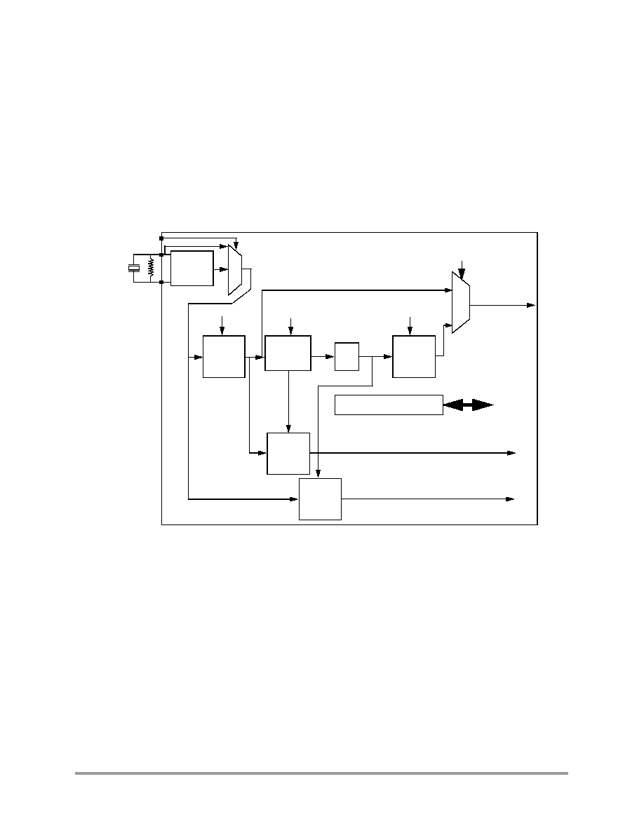
Introduction
56F8346 Technical Data
31
Preliminary
Part 3 On-Chip Clock Synthesis (OCCS)
3.1 Introduction
Refer to the OCCS chapter of the 56F8300 Peripheral User Manual for a full description of the
OCCS. The material contained here identifies the specific features of the OCCS design that apply
to the 56F8346 part.
Figure 3-1
shows the specific OCCS block diagram to reference from the
OCCS chapter in the 56F8300 Peripheral User Manual.
Figure 3-1 OCCS Block Diagram
MUX
EXTAL
XTAL
F
EED
BAC
K
LCK
Prescaler CLK
Postscaler CLK
F
OUT/2
Crystal
OSC
Loss of
Reference
Clock
Detector
Lock
Detector
ZSRC
Bus Interface & Control
F
OUT
F
RE
F
PLLDB
PLLCOD
PLLCID
Bus
Interface
Loss of Reference
Clock Interrupt
SYS_CLK2
Source to SIM
MU
X
CLKMODE
÷
2
Prescaler
÷
(
1,2,4,8
)
Postscaler
÷
(
1,2,4,8
)
MS
TR_
O
S
C
PLL
x (1 to 128)
F
r
e
e
s
c
a
l
e
S
e
m
i
c
o
n
d
u
c
t
o
r
,
I
Freescale Semiconductor, Inc.
For More Information On This Product,
Go to: www.freescale.com
n
c
.
.
.
32
56F8346 Technical Data
Preliminary
3.2 External Clock Operation
The 56F8346 system clock can be derived from an external crystal, ceramic resonator, or an
external system clock signal. To generate a reference frequency using the internal oscillator, a
reference crystal or ceramic resonator, must be connected between the EXTAL and XTAL pins.
3.2.1
Crystal Oscillator
The internal oscillator is designed to interface with a parallel-resonant crystal resonator in the
frequency range specified for the external crystal in
Table 10-15
. A recommended crystal
oscillator circuit is shown in
Figure 3-2
. Follow the crystal supplier's recommendations when
selecting a crystal, since crystal parameters determine the component values required to provide
maximum stability and reliable start-up. The crystal and associated components should be mounted
as near as possible to the EXTAL and XTAL pins to minimize output distortion and start-up
stabilization time.
Figure 3-2 Connecting to a Crystal Oscillator
Note:
The OCCS_COHL bit must be set to 1 when a crystal oscillator is used. The reset condition on
the OCCS_COHL bit is 0. Please see the COHL bit in the Oscillator Control (OSCTL)
register, discussed in the 56F8300 Peripheral User Manual.
Sample External Crystal Parameters:
R
z
= 750 K
Note: If the operating temperature range is limited to
below 85
o
C
(105
o
C junction), then R
z
= 10 Meg
CLKMODE = 0
EXTAL XTAL
R
z
CL1
CL2
Crystal Frequency = 4 - 8MHz (optimized for 8MHz)
EXTAL XTAL
R
z
F
r
e
e
s
c
a
l
e
S
e
m
i
c
o
n
d
u
c
t
o
r
,
I
Freescale Semiconductor, Inc.
For More Information On This Product,
Go to: www.freescale.com
n
c
.
.
.
Registers
56F8346 Technical Data
33
Preliminary
3.2.2
Ceramic Resonator (Default)
It is also possible to drive the internal oscillator with a ceramic resonator, assuming the overall
system design can tolerate the reduced signal integrity. A typical ceramic resonator circuit is shown
in
Figure 3-3
. Refer to the supplier's recommendations when selecting a ceramic resonator and
associated components. The resonator and components should be mounted as near as possible to
the EXTAL and XTAL pins.
Figure 3-3 Connecting a Ceramic Resonator
Note:
The OCCS_COHL bit must be set to 0 when a ceramic resonator is used. The reset condition
on the OCCS_COHL bit is 0. Please see the COHL bit in the Oscillator Control (OSCTL)
register, discussed in the 56F8300 Peripheral User Manual.
3.2.3
External Clock Source
The recommended method of connecting an external clock is given in
Figure 3-4
. The external
clock source is connected to XTAL and the EXTAL pin is grounded. Set OCCS_COHL bit high
when using an external clock source as well.
Figure 3-4 Connecting an External Clock Register
3.3 Registers
When referring to the register definitions for the OCCS in the 56F8300 Peripheral User Manual,
use the register definitions without the internal Relaxation Oscillator, since the 56F8346 does
NOT contain this oscillator.
EXTAL
XTAL
R
z
Sample External Ceramic Resonator Parameters:
R
z
= 750 K
EXTAL
XTAL
R
z
C1
CL1
CL2
C2
Resonator Frequency = 4 - 8MHz (optimized for 8MHz)
3 Terminal
2 Terminal
CLKMODE = 0
56F8346
XTAL
EXTAL
External
V
SS
Clock
Note: When using an external clocking source
with this configuration, the input "CLKMODE"
should be high and the COHL bit in the OSCTL
register should be set to 1.
F
r
e
e
s
c
a
l
e
S
e
m
i
c
o
n
d
u
c
t
o
r
,
I
Freescale Semiconductor, Inc.
For More Information On This Product,
Go to: www.freescale.com
n
c
.
.
.

34
56F8346 Technical Data
Preliminary
Part 4 Memory Map
4.1 Introduction
The 56F8346 device is a 16-bit motor-control chip based on the 56800E core. It uses a
Harvard-style architecture with two independent memory spaces for Data and Program. On-chip
RAM and Flash memories are used in both spaces.
This section provides memory maps for:
·
Program Address Space, including the Interrupt Vector Table
·
Data Address Space, including the EOnCE Memory and Peripheral Memory Maps
On-chip memory sizes for each device are summarized in
Table 4-1
. Flash memories' restrictions
are identified in the "Use Restrictions" column of
Table 4-1
.
Table 4-1 Chip Memory Configurations
On-Chip Memory
56F8346
Use Restrictions
Program Flash
128KB
Erase / Program via Flash interface unit and word writes to CDBW
Data Flash
8KB
Erase / Program via Flash interface unit and word writes to CDBW. Data
Flash can be read via either CDBR or XDB2, but not by both simultaneously
Program RAM
4KB
None
Data RAM
8KB
None
Program Boot Flash
8KB
Erase / Program via Flash Interface unit and word to CDBW
F
r
e
e
s
c
a
l
e
S
e
m
i
c
o
n
d
u
c
t
o
r
,
I
Freescale Semiconductor, Inc.
For More Information On This Product,
Go to: www.freescale.com
n
c
.
.
.

Program Map
56F8346 Technical Data
35
Preliminary
4.2 Program Map
The operating mode control bits (MA and MB) in the Operating Mode Register (OMR) control the
Program memory map. At reset, these bits are set as indicated in
Table 4-2
.
Table 4-4
shows the
memory map configurations that are possible at reset. After reset, the OMR MA bit can be changed
and will have an effect on the P-space memory map, as shown in
Table 4-3
. Changing the OMR
MB bit will have no effect.
The 56F8346's external memory interface (EMI) can operate much like the 56F80x family's EMI,
or it can be operated in a mode similar to that used on other products in the 56800E family. Initially,
CS0 and CS1 are configured as PS and DS, in a mode compatible with earlier 56800 devices.
Eighteen address lines are required to shadow the first 192K of internal program space when
booting externally for development purposes. Therefore, the entire complement of on-chip
memory cannot be accessed using a 16-bit 56800-compatible address bus. To address this
situation, the EMI_MODE pin can be used to configure four GPIO pins as Address[19:16] upon
reset (only one of these pins [A16] is usable in the 56F8346).
The EMI_MODE pin also affects the reset vector address, as provided in
Table 4-4
. Additional
pins must be configured as address or chip select signals to access addresses at P:$10 0000 and
above.
Table 4-2 OMR MB/MA Value at Reset
OMR MB =
Flash Secured
State
1,
2
1.
This bit is only configured at reset. If the Flash secured state changes, this will not be reflected in MB until the next reset.
2.
Changing MB in software will not affect Flash memory security.
OMR MA =
EXTBOOT Pin
Chip Operating Mode
0
0
Mode 0 Internal Boot; EMI is configured to use 16 address lines; Flash
Memory is secured; external P-space is not allowed; the EOnCE is disabled
0
1
Not valid; cannot boot externally if the Flash is secured and will actually
configure to 00 state
1
0
Mode 0 Internal Boot; EMI is configured to use 16 address lines
1
1
Mode 1 External Boot; Flash Memory is not secured; EMI configuration is
determined by the state of the EMI_MODE pin
Table 4-3 Changing OMR MA Value During Normal Operation
OMR MA
Chip Operating Mode
0
Use internal P-space memory map configuration
1
Use external P-space memory map configuration If MB = 0 at reset, changing this bit has no
effect.
F
r
e
e
s
c
a
l
e
S
e
m
i
c
o
n
d
u
c
t
o
r
,
I
Freescale Semiconductor, Inc.
For More Information On This Product,
Go to: www.freescale.com
n
c
.
.
.

36
56F8346 Technical Data
Preliminary
4.3 Interrupt Vector Table
Table 4-5
provides the reset and interrupt priority structure, including on-chip peripherals. The
table is organized with higher-priority vectors at the top and lower-priority interrupts lower in the
table. The priority of an interrupt can be assigned to different levels, as indicated, allowing some
control over interrupt priorities. All level 3 interrupts will be serviced before level 2, and so on. For
a selected priority level, the lowest vector number has the highest priority.
The location of the vector table is determined by the Vector Base Address (VBA) register. Please
see
Section 5.6.12
for the reset value of the VBA.
In some configurations, the reset address and COP reset address will correspond to vector 0 and 1
of the interrupt vector table. In these instances, the first two locations in the vector table must
contain branch or JMP instructions. All other entries must contain JSR instructions.
Table 4-4 Program Memory Map at Reset
Begin/End
Address
Mode 0 (MA = 0)
Mode 1
1
(MA = 1)
1.
If Flash Security Mode is enabled, EXTBOOT Mode 1 cannot be used. See Security Features,
Part 7
.
Internal Boot
External Boot
Internal Boot
16-Bit External Address Bus
EMI_MODE = 0
2
,
3
16-Bit External Address Bus
2.
This mode provides maximum compatibility with 56F80x parts while operating externally.
3.
"EMI_MODE =0" when EMI_MODE pin is tied to ground at boot up.
EMI_MODE = 1
4
20-Bit External Address Bus
4.
"EMI_MODE =1" when EMI_MODE pin is tied to V
DD
at boot up.
P:$1F FFFF
P:$10 0000
External Program Memory
5
5.
Not accessible in reset configuration, since the address is above P:$00 FFFF. The higher bit address/GPIO (and/or chip
selects) pins must be reconfigured before this external memory is accessible.
External Program Memory
5
External Program Memory
5
P:$0F FFFF
P:$03 0000
External Program RAM
COP Reset Address = 02 0002
6
Boot Location = 02 0000
6
6.
Booting from this external address allows prototyping of the internal Boot Flash.
P:$02 FFFF
P:$02 F800
On-Chip Program RAM
4KB
P:$02 F7FF
P:$02 1000
Reserved
116KB
P:$02 0FFF
P:$02 0000
Boot Flash
8KB
COP Reset Address = 02 0002
Boot Location = 02 0000
Boot Flash
8KB
(Not Used for Boot in this Mode)
P:$01 FFFF
P:$01 0000
External Program RAM
5
Internal Program Flash
7
128KB
7.
The internal Program Flash is relocated in this mode making it accessible.
P:$00 FFFF
P:$00 0000
Internal Program Flash
128KB
External Program RAM
COP Reset Address = 00 0002
Boot Location = 00 0000
F
r
e
e
s
c
a
l
e
S
e
m
i
c
o
n
d
u
c
t
o
r
,
I
Freescale Semiconductor, Inc.
For More Information On This Product,
Go to: www.freescale.com
n
c
.
.
.

Interrupt Vector Table
56F8346 Technical Data
37
Preliminary
Table 4-5 Interrupt Vector Table Contents
1
Peripheral
Vector
Number
Priority
Level
Vector Base
Address +
Interrupt Function
Reserved for Reset Overlay
2
Reserved for COP Reset Overlay
2
core
2
3
P:$04
Illegal Instruction
core
3
3
P:$06
SW Interrupt 3
core
4
3
P:$08
HW Stack Overflow
core
5
3
P:$0A
Misaligned Long Word Access
core
6
1-3
P:$0C
OnCE Step Counter
core
7
1-3
P:$0E
OnCE Breakpoint Unit 0
Reserved
core
9
1-3
P:$12
OnCE Trace Buffer
core
10
1-3
P:$14
OnCE Transmit Register Empty
core
11
1-3
P:$16
OnCE Receive Register Full
Reserved
core
14
2
P:$1C
SW Interrupt 2
core
15
1
P:$1E
SW Interrupt 1
core
16
0
P:$20
SW Interrupt 0
core
17
0-2
P:$22
IRQA
core
18
0-2
P:$24
IRQB
Reserved
LVI
20
0-2
P:$28
Low Voltage Detector (power sense)
PLL
21
0-2
P:$2A
PLL
FM
22
0-2
P:$2C
FM Access Error Interrupt
FM
23
0-2
P:$2E
FM Command Complete
FM
24
0-2
P:$30
FM Command, data and address Buffers Empty
Reserved
FLEXCAN
26
0-2
P:$34
FLEXCAN Bus Off
FLEXCAN
27
0-2
P:$36
FLEXCAN Error
FLEXCAN
28
0-2
P:$38
FLEXCAN Wake Up
FLEXCAN
29
0-2
P:$3A
FLEXCAN Message Buffer Interrupt
GPIOF
30
0-2
P:$3C
GPIO F
GPIOE
31
0-2
P:$3E
GPIO E
GPIOD
32
0-2
P:$40
GPIO D
GPIOC
33
0-2
P:$42
GPIO C
GPIOB
34
0-2
P:$44
GPIO B
F
r
e
e
s
c
a
l
e
S
e
m
i
c
o
n
d
u
c
t
o
r
,
I
Freescale Semiconductor, Inc.
For More Information On This Product,
Go to: www.freescale.com
n
c
.
.
.

38
56F8346 Technical Data
Preliminary
GPIOA
35
0-2
P:$46
GPIO A
Reserved
SPI1
38
0-2
P:$4C
SPI 1 Receiver Full
SPI1
39
0-2
P:$4E
SPI 1 Transmitter Empty
SPI0
40
0-2
P:$50
SPI 0 Receiver Full
SPI0
41
0-2
P:$52
SPI 0 Transmitter Empty
SCI1
42
0-2
P:$54
SCI 1 Transmitter Empty
SCI1
43
0-2
P:$56
SCI 1 Transmitter Idle
Reserved
SCI1
45
0-2
P:$5A
SCI 1 Receiver Error
SCI1
46
0-2
P:$5C
SCI 1 Receiver Full
DEC1
47
0-2
P:$5E
Quadrature Decoder #1 Home Switch or Watchdog
DEC1
48
0-2
P:$60
Quadrature Decoder #1 INDEX Pulse
DEC0
49
0-2
P:$62
Quadrature Decoder #0 Home Switch or Watchdog
DEC0
50
0-2
P:$64
Quadrature Decoder #0 INDEX Pulse
Reserved
TMRD
52
0-2
P:$68
Timer D, Channel 0
TMRD
53
0-2
P:$6A
Timer D, Channel 1
TMRD
54
0-2
P:$6C
Timer D, Channel 2
TMRD
55
0-2
P:$6E
Timer D, Channel 3
TMRC
56
0-2
P:$70
Timer C, Channel 0
TMRC
57
0-2
P:$72
Timer C, Channel 1
TMRC
58
0-2
P:$74
Timer C, Channel 2
TMRC
59
0-2
P:$76
Timer C, Channel 3
TMRB
60
0-2
P:$78
Timer B, Channel 0
TMRB
61
0-2
P:$7A
Timer B, Channel 1
TMRB
62
0-2
P:$7C
Timer B, Channel 2
TMRB
63
0-2
P:$7E
Timer B, Channel 3
TMRA
64
0-2
P:$80
Timer A, Channel 0
TMRA
65
0-2
P:$82
Timer A, Channel 1
TMRA
66
0-2
P:$84
Timer A, Channel 2
TMRA
67
0-2
P:$86
Timer A, Channel 3
SCI0
68
0-2
P:$88
SCI 0 Transmitter Empty
SCI0
69
0-2
P:$8A
SCI 0 Transmitter Idle
Table 4-5 Interrupt Vector Table Contents
1
(Continued)
Peripheral
Vector
Number
Priority
Level
Vector Base
Address +
Interrupt Function
F
r
e
e
s
c
a
l
e
S
e
m
i
c
o
n
d
u
c
t
o
r
,
I
Freescale Semiconductor, Inc.
For More Information On This Product,
Go to: www.freescale.com
n
c
.
.
.

Data Map
56F8346 Technical Data
39
Preliminary
4.4 Data Map
Reserved
SCI0
71
0-2
P:$8E
SCI 0 Receiver Error
SCI0
72
0-2
P:$90
SCI 0 Receiver Full
ADCB
73
0-2
P:$92
ADC B Conversion Compete
ADCA
74
0-2
P:$94
ADC A Conversion Complete
ADCB
75
0-2
P:$96
ADC B Zero Crossing of Limit Error
ADCA
76
0-2
P:$98
ADC A Zero Crossing of Limit Error
PWMB
77
0-2
P:$9A
Reload PWM B
PWMA
78
0-2
P:$9C
Reload PWM A
PWMB
79
0-2
P:$9E
PWM B Fault
PWMA
80
0-2
P:$A0
PWM A Fault
core
81
- 1
P:$A2
SW Interrupt LP
1.
Two words are allocated for each entry in the vector table. This does not allow the full address range to be referenced
from the vector table, providing only 19 bits of address.
2. If the VBA is set to 0200 (or VBA = 0000 for Mode 1, EMI_MODE = 0), the first two locations of the vector table are the chip
reset addresses; therefore, these locations are not interrupt vectors.
2.
Table 4-6 Data Memory Map
1
1.
All addresses are 16-bit Word addresses, not byte addresses.
Begin/End
Address
EX = 0
2
2.
In the Operation Mode Register (OMR).
EX = 1
X:$FF FFFF
X:$FF FF00
EOnCE
256 locations allocated
EOnCE
256 locations allocated
X:$FF FEFF
X:$01 0000
External Memory
External Memory
X:$00 FFFF
X:$00 F000
On-Chip Peripherals
4096 locations allocated
On-Chip Peripherals
4096 locations allocated
X:$00 EFFF
X:$00 2000
External Memory
External Memory
X:$00 1FFF
X:$00 1000
On-Chip Data Flash
8KB
X:$00 0FFF
X:$00 0000
On-Chip Data RAM
8KB
3
3.
The Data RAM is organized as a 2K x 32-bit memory to allow single-cycle long-word operations.
Table 4-5 Interrupt Vector Table Contents
1
(Continued)
Peripheral
Vector
Number
Priority
Level
Vector Base
Address +
Interrupt Function
F
r
e
e
s
c
a
l
e
S
e
m
i
c
o
n
d
u
c
t
o
r
,
I
Freescale Semiconductor, Inc.
For More Information On This Product,
Go to: www.freescale.com
n
c
.
.
.
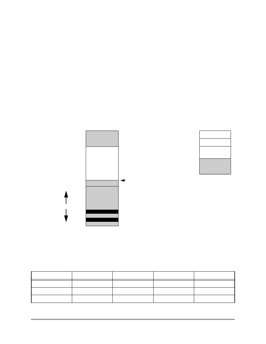
40
56F8346 Technical Data
Preliminary
4.5 Flash Memory Map
Figure 4-1
illustrates the Flash Memory (FM) map on the system bus.
The Flash Memory is divided into three functional blocks. The Program and boot memories reside
on the Program Memory buses. They are controlled by one set of banked registers. Data Memory
Flash resides on the Data Memory buses and is controlled separately by own set of banked
registers.
The top nine words of the Program Memory Flash are treated as special memory locations. The
content of these words is used to control the operation of the Flash Controller. Because these words
are part of the Flash Memory content, their state is maintained during power-down and reset.
During chip initialization, the content of these memory locations is loaded into Flash Memory
control registers, detailed in the Flash Memory chapter of the 56F8300 Peripheral User Manual.
In the 56F8346, these configuration parameters are located between $00_FFF7 and $00_FFFF.
Figure 4-1 Flash Array Memory Maps
Table 4-7
shows the page and sector sizes used within each Flash memory block on the chip.
Please see 56F8300 Peripheral User Manual for additional Flash information.
Table 4-7. Flash Memory Partitions
Flash Size
Sectors
Sector Size
Page Size
Program Flash
128KB
16
4K x 16 bits
512 x 16 bits
Data Flash
8KB
16
256 x 16 bits
256 x 16 bits
Boot Flash
8KB
4
1K x 16 bits
256 x 16 bits
BOOT_FLASH_START = $02_0000
BOOT_FLASH_START + $1FFF
Block 0 Odd
Block 0 Even
PROG_FLASH_START + $00_FFFF
.
.
.
8KB
Boot
Reserved
Configure Field
PROG_FLASH_START + $00_FFF7
PROG_FLASH_START + $00_FFF6
128K Bytes
PROG_FLASH_START = $00_0000
FM_PROG_MEM_TOP = $00_FFFF
BLOCK 0 Odd (2 Bytes) $00_0003
BLOCK 0 Even (2 Bytes) $00_0002
BLOCK 0 Odd (2 Bytes) $00_0001
BLOCK 0 Even (2 Bytes) $00_0000
FM_BASE + $14
Banked Registers
Unbanked Registers
8KB
FM_BASE + $00
DATA_FLASH_START + $0FFF
DATA_FLASH_START + $0000
Data Memory
Program Memory
F
r
e
e
s
c
a
l
e
S
e
m
i
c
o
n
d
u
c
t
o
r
,
I
Freescale Semiconductor, Inc.
For More Information On This Product,
Go to: www.freescale.com
n
c
.
.
.

EOnCE Memory Map
56F8346 Technical Data
41
Preliminary
4.6 EOnCE Memory Map
4.7 Peripheral Memory Mapped Registers
On-chip peripheral registers are part of the data memory map on the 56800E series. These locations
may be accessed with the same addressing modes used for ordinary data memory, except all
peripheral registers should be read/written using word accesses only.
Table 4-8 EOnCE Memory Map
Address
Register Acronym
Register Name
Reserved
X:$FF FF8A
OESCR
External Signal Control Register
Reserved
X:$FF FF8E
OBCNTR
Breakpoint Unit [0] Counter
Reserved
X:$FF FF90
OBMSK (32 bits)
Breakpoint 1 Unit [0] Mask Register
X:$FF FF91
--
Breakpoint 1 Unit [0] Mask Register
X:$FF FF92
OBAR2 (32 bits)
Breakpoint 2 Unit [0] Address Register
X:$FF FF93
--
Breakpoint 2 Unit [0] Address Register
X:$FF FF94
OBAR1 (24 bits)
Breakpoint 1 Unit [0] Address Register
X:$FF FF95
--
Breakpoint 1 Unit [0] Address Register
X:$FF FF96
OBCR (24 bits)
Breakpoint Unit [0] Control Register
X:$FF FF97
--
Breakpoint Unit [0] Control Register
X:$FF FF98
OTB (21-24 bits/stage)
Trace Buffer Register Stages
X:$FF FF99
--
Trace Buffer Register Stages
X:$FF FF9A
OTBPR (8 bits)
Trace Buffer Pointer Register
X:$FF FF9B
OTBCR
Trace Buffer Control Register
X:$FF FF9C
OBASE (8 bits)
Peripheral Base Address Register
X:$FF FF9D
OSR
Status Register
X:$FF FF9E
OSCNTR (24 bits)
Instruction Step Counter
X:$FF FF9F
--
Instruction Step Counter
X:$FF FFA0
OCR (bits)
Control Register
Reserved
X:$FF FFFC
OCLSR (8 bits)
Core Lock / Unlock Status Register
X:$FF FFFD
OTXRXSR (8 bits)
Transmit and Receive Status and Control Register
X:$FF FFFE
OTX / ORX (32 bits)
Transmit Register / Receive Register
X:$FF FFFF
OTX1 / ORX1
Transmit Register Upper Word
Receive Register Upper Word
F
r
e
e
s
c
a
l
e
S
e
m
i
c
o
n
d
u
c
t
o
r
,
I
Freescale Semiconductor, Inc.
For More Information On This Product,
Go to: www.freescale.com
n
c
.
.
.

42
56F8346 Technical Data
Preliminary
Table 4-9
summarizes base addresses for the set of peripherals on the 56F8346 device. Peripherals
are listed in order of the base address.
The following tables list all of the peripheral registers required to control or access the peripherals.
Table 4-9 Data Memory Peripheral Base Address Map Summary
Peripheral
Prefix
Base Address
Table Number
External Memory Interface
EMI
X:$00 F020
4-10
Timer A
TMRA
X:$00 F040
4-11
Timer B
TMRB
X:$00 F080
4-12
Timer C
TMRC
X:$00 F0C0
4-13
Timer D
TMRD
X:$00 F100
4-14
PWM A
PWMA
X:$00 F140
4-15
PWM B
PWMB
X:$00 F160
4-16
Quadrature Decoder 0
DEC0
X:$00 F180
4-17
Quadrature Decoder 1
DEC1
X:$00 F190
4-18
ITCN
ITCN
X:$00 F1A0
4-19
ADC A
ADCA
X:$00 F200
4-20
ADC B
ADCB
X:$00 F240
4-21
Temperature Sensor
TSENSOR
X:$00 F270
4-22
SCI #0
SCI0
X:$00 F280
4-23
SCI #1
SCI1
X:$00 F290
4-24
SPI #0
SPI0
X:$00 F2A0
4-25
SPI #1
SPI1
X:$00 F2B0
4-26
COP
COP
X:$00 F2C0
4-27
PLL, OSC
CLKGEN
X:$00 F2D0
4-28
GPIO Port A
GPIOA
X:$00 F2E0
4-29
GPIO Port B
GPIOB
X:$00 F300
4-30
GPIO Port C
GPIOC
X:$00 F310
4-31
GPIO Port D
GPIOD
X:$00 F320
4-32
GPIO Port E
GPIOE
X:$00 F330
4-33
GPIO Port F
GPIOF
X:$00 F340
4-34
SIM
SIM
X:$00 F350
4-35
Power Supervisor
LVI
X:$00 F360
4-36
FM
FM
X:$00 F400
4-37
FlexCAN
FC
X:$00 F800
4-38
F
r
e
e
s
c
a
l
e
S
e
m
i
c
o
n
d
u
c
t
o
r
,
I
Freescale Semiconductor, Inc.
For More Information On This Product,
Go to: www.freescale.com
n
c
.
.
.

Peripheral Memory Mapped Registers
56F8346 Technical Data
43
Preliminary
Table 4-10 External Memory Integration Registers Address Map
(EMI_BASE = $00 F020)
Register Acronym
Address Offset
Register Description
Reset Value
CSBAR 0
$0
Chip Select Base Address Register 0
CSBAR 1
$1
Chip Select Base Address Register 1
CSBAR 2
$2
Chip Select Base Address Register 2
CSBAR 3
$3
Chip Select Base Address Register 3
CSBAR 4
$4
Chip Select Base Address Register 4
CSBAR 5
$5
Chip Select Base Address Register 5
CSBAR 6
$6
Chip Select Base Address Register 6
CSBAR 7
$7
Chip Select Base Address Register 7
CSOR 0
$8
Chip Select Option Register 0
0x5FCB programmed for
chip select for program
space, word wide, read and
write, 11 waits
CSOR 1
$9
Chip Select Option Register 1
0x5FAB programmed for
chip select for data space,
word wide, read and write,
11 waits
CSOR 2
$A
Chip Select Option Register 2
CSOR 3
$B
Chip Select Option Register 3
CSOR 4
$C
Chip Select Option Register 4
CSOR 5
$D
Chip Select Option Register 5
CSOR 6
$E
Chip Select Option Register 6
CSOR 7
$F
Chip Select Option Register 7
CSTC 0
$10
Chip Select Timing Control Register 0
CSTC 1
$11
Chip Select Timing Control Register 1
CSTC 2
$12
Chip Select Timing Control Register 2
CSTC 3
$13
Chip Select Timing Control Register 3
CSTC 4
$14
Chip Select Timing Control Register 4
CSTC 5
$15
Chip Select Timing Control Register 5
CSTC 6
$16
Chip Select Timing Control Register 6
CSTC 7
$17
Chip Select Timing Control Register 7
BCR
$18
Bus Control Register
0x016B sets the default
number of wait states to 11
for both read and write
accesses
F
r
e
e
s
c
a
l
e
S
e
m
i
c
o
n
d
u
c
t
o
r
,
I
Freescale Semiconductor, Inc.
For More Information On This Product,
Go to: www.freescale.com
n
c
.
.
.

44
56F8346 Technical Data
Preliminary
Table 4-11 Quad Timer A Registers Address Map
(TMRA_BASE = $00 F040)
Register Acronym
Address Offset
Register Description
TMRA0_CMP1
$0
Compare Register 1
TMRA0_CMP2
$1
Compare Register 2
TMRA0_CAP
$2
Capture Register
TMRA0_LOAD
$3
Load Register
TMRA0_HOLD
$4
Hold Register
TMRA0_CNTR
$5
Counter Register
TMRA0_CTRL
$6
Control Register
TMRA0_SCR
$7
Status and Control Register
TMRA0_CMPLD1
$8
Comparator Load Register 1
TMRA0_CMPLD2
$9
Comparator Load Register 2
TMRA0_COMSCR
$A
Comparator Status and Control Register
Reserve
TMRA1_CMP1
$10
Compare Register 1
TMRA1_CMP2
$11
Compare Register 2
TMRA1_CAP
$12
Capture Register
TMRA1_LOAD
$13
Load Register
TMRA1_HOLD
$14
Hold Register
TMRA1_CNTR
$15
Counter Register
TMRA1_CTRL
$16
Control Register
TMRA1_SCR
$17
Status and Control Register
TMRA1_CMPLD1
$18
Comparator Load Register 1
TMRA1_CMPLD2
$19
Comparator Load Register 2
TMRA1_COMSCR
$1A
Comparator Status and Control Register
Reserved
TMRA2_CMP1
$20
Compare Register 1
TMRA2_CMP2
$21
Compare Register 2
TMRA2_CAP
$22
Capture Register
TMRA2_LOAD
$23
Load Register
TMRA2_HOLD
$24
Hold Register
TMRA2_CNTR
$25
Counter Register
TMRA2_CTRL
$26
Control Register
TMRA2_SCR
$27
Status and Control Register
TMRA2_CMPLD1
$28
Comparator Load Register 1
F
r
e
e
s
c
a
l
e
S
e
m
i
c
o
n
d
u
c
t
o
r
,
I
Freescale Semiconductor, Inc.
For More Information On This Product,
Go to: www.freescale.com
n
c
.
.
.

Peripheral Memory Mapped Registers
56F8346 Technical Data
45
Preliminary
TMRA2_CMPLD2
$29
Comparator Load Register 2
TMRA2_COMSCR
$2A
Comparator Status and Control Register
Reserved
TMRA3_CMP1
$30
Compare Register 1
TMRA3_CMP2
$31
Compare Register 2
TMRA3_CAP
$32
Capture Register
TMRA3_LOAD
$33
Load Register
TMRA3_HOLD
$34
Hold Register
TMRA3_CNTR
$35
Counter Register
TMRA3_CTRL
$36
Control Register
TMRA3_SCR
$37
Status and Control Register
TMRA3_CMPLD1
$38
Comparator Load Register 1
TMRA3_CMPLD2
$39
Comparator Load Register 2
TMRA3_COMSC
$3A
Comparator Status and Control Register
Table 4-12 Quad Timer B Registers Address Map
(TMRB_BASE = $00 F080)
Register Acronym
Address Offset
Register Description
TMRB0_CMP1
$0
Compare Register 1
TMRB0_CMP2
$1
Compare Register 2
TMRB0_CAP
$2
Capture Register
TMRB0_LOAD
$3
Load Register
TMRB0_HOLD
$4
Hold Register
TMRB0_CNTR
$5
Counter Register
TMRB0_CTRL
$6
Control Register
TMRB0_SCR
$7
Status and Control Register
TMRB0_CMPLD1
$8
Comparator Load Register 1
TMRB0_CMPLD2
$9
Comparator Load Register 2
TMRB0_COMSCR
$A
Comparator Status and Control Register
Reserved
TMRB1_CMP1
$10
Compare Register 1
TMRB1_CMP2
$11
Compare Register 2
TMRB1_CAP
$12
Capture Register
TMRB1_LOAD
$13
Load Register
Table 4-11 Quad Timer A Registers Address Map
(TMRA_BASE = $00 F040) (Continued)
Register Acronym
Address Offset
Register Description
F
r
e
e
s
c
a
l
e
S
e
m
i
c
o
n
d
u
c
t
o
r
,
I
Freescale Semiconductor, Inc.
For More Information On This Product,
Go to: www.freescale.com
n
c
.
.
.

46
56F8346 Technical Data
Preliminary
TMRB1_HOLD
$14
Hold Register
TMRB1_CNTR
$15
Counter Register
TMRB1_CTRL
$16
Control Register
TMRB1_SCR
$17
Status and Control Register
TMRB1_CMPLD1
$18
Comparator Load Register 1
TMRB1_CMPLD2
$19
Comparator Load Register 2
TMRB1_COMSCR
$1A
Comparator Status and Control Register
Reserved
TMRB2_CMP1
$20
Compare Register 1
TMRB2_CMP2
$21
Compare Register 2
TMRB2_CAP
$22
Capture Register
TMRB2_LOAD
$23
Load Register
TMRB2_HOLD
$24
Hold Register
TMRB2_CNTR
$25
Counter Register
TMRB2_CTRL
$26
Control Register
TMRB2_SCR
$27
Status and Control Register
TMRB2_CMPLD1
$28
Comparator Load Register 1
TMRB2_CMPLD2
$29
Comparator Load Register 2
TMRB2_COMSCR
$2A
Comparator Status and Control Register
Reserved
TMRB3_CMP1
$30
Compare Register 1
TMRB3_CMP2
$31
Compare Register 2
TMRB3_CAP
$32
Capture Register
TMRB3_LOAD
$33
Load Register
TMRB3_HOLD
$34
Hold Register
TMRB3_CNTR
$35
Counter Register
TMRB3_CTRL
$36
Control Register
TMRB3_SCR
$37
Status and Control Register
TMRB3_CMPLD1
$38
Comparator Load Register 1
TMRB3_CMPLD2
$39
Comparator Load Register 2
TMRB3_COMSCR
$3A
Comparator Status and Control Register
Table 4-12 Quad Timer B Registers Address Map
(TMRB_BASE = $00 F080) (Continued)
Register Acronym
Address Offset
Register Description
F
r
e
e
s
c
a
l
e
S
e
m
i
c
o
n
d
u
c
t
o
r
,
I
Freescale Semiconductor, Inc.
For More Information On This Product,
Go to: www.freescale.com
n
c
.
.
.

Peripheral Memory Mapped Registers
56F8346 Technical Data
47
Preliminary
Table 4-13 Quad Timer C Registers Address Map
(TMRC_BASE = $00 F0C0)
Register Acronym
Address Offset
Register Description
TMRC0_CMP1
$0
Compare Register 1
TMRC0_CMP2
$1
Compare Register 2
TMRC0_CAP
$2
Capture Register
TMRC0_LOAD
$3
Load Register
TMRC0_HOLD
$4
Hold Register
TMRC0_CNTR
$5
Counter Register
TMRC0_CTRL
$6
Control Register
TMRC0_SCR
$7
Status and Control Register
TMRC0_CMPLD1
$8
Comparator Load Register 1
TMRC0_CMPLD2
$9
Comparator Load Register 2
TMRC0_COMSCR
$A
Comparator Status and Control Register
Reserved
TMRC1_CMP1
$10
Compare Register 1
TMRC1_CMP2
$11
Compare Register 2
TMRC1_CAP
$12
Capture Register
TMRC1_LOAD
$13
Load Register
TMRC1_HOLD
$14
Hold Register
TMRC1_CNTR
$15
Counter Register
TMRC1_CTRL
$16
Control Register
TMRC1_SCR
$17
Status and Control Register
TMRC1_CMPLD1
$18
Comparator Load Register 1
TMRC1_CMPLD2
$19
Comparator Load Register 2
TMRC1_COMSCR
$1A
Comparator Status and Control Register
Reserved
TMRC2_CMP1
$20
Compare Register 1
TMRC2_CMP2
$21
Compare Register 2
TMRC2_CAP
$22
Capture Register
TMRC2_LOAD
$23
Load Register
TMRC2_HOLD
$24
Hold Register
TMRC2_CNTR
$25
Counter Register
TMRC2_CTRL
$26
Control Register
TMRC2_SCR
$27
Status and Control Register
TMRC2_CMPLD1
$28
Comparator Load Register 1
TMRC2_CMPLD2
$29
Comparator Load Register 2
F
r
e
e
s
c
a
l
e
S
e
m
i
c
o
n
d
u
c
t
o
r
,
I
Freescale Semiconductor, Inc.
For More Information On This Product,
Go to: www.freescale.com
n
c
.
.
.
48
56F8346 Technical Data
Preliminary
TMRC2_COMSCR
$2A
Comparator Status and Control Register
Reserved
TMRC3_CMP1
$30
Compare Register 1
TMRC3_CMP2
$31
Compare Register 2
TMRC3_CAP
$32
Capture Register
TMRC3_LOAD
$33
Load Register
TMRC3_HOLD
$34
Hold Register
TMRC3_CNTR
$35
Counter Register
TMRC3_CTRL
$36
Control Register
TMRC3_SCR
$37
Status and Control Register
TMRC3_CMPLD1
$38
Comparator Load Register 1
TMRC3_CMPLD2
$39
Comparator Load Register 2
TMRC3_COMSCR
$3A
Comparator Status and Control Register
Table 4-14 Quad Timer D Registers Address Map
(TMRD_BASE = $00 F100)
Register Acronym
Address Offset
Register Description
TMRD0_CMP1
$0
Compare Register 1
TMRD0_CMP2
$1
Compare Register 2
TMRD0_CAP
$2
Capture Register
TMRD0_LOAD
$3
Load Register
TMRD0_HOLD
$4
Hold Register
TMRD0_CNTR
$5
Counter Register
TMRD0_CTRL
$6
Control Register
TMRD0_SCR
$7
Status and Control Register
TMRD0_CMPLD1
$8
Comparator Load Register 1
TMRD0_CMPLD2
$9
Comparator Load Register 2
TMRD0_COMSCR
$A
Comparator Status and Control Register
Reserved
TMRD1_CMP1
$10
Compare Register 1
TMRD1_CMP2
$11
Compare Register 2
TMRD1_CAP
$12
Capture Register
TMRD1_LOAD
$13
Load Register
TMRD1_HOLD
$14
Hold Register
Table 4-13 Quad Timer C Registers Address Map
(TMRC_BASE = $00 F0C0) (Continued)
Register Acronym
Address Offset
Register Description
F
r
e
e
s
c
a
l
e
S
e
m
i
c
o
n
d
u
c
t
o
r
,
I
Freescale Semiconductor, Inc.
For More Information On This Product,
Go to: www.freescale.com
n
c
.
.
.

Peripheral Memory Mapped Registers
56F8346 Technical Data
49
Preliminary
TMRD1_CNTR
$15
Counter Register
TMRD1_CTRL
$16
Control Register
TMRD1_SCR
$17
Status and Control Register
TMRD1_CMPLD1
$18
Comparator Load Register 1
TMRD1_CMPLD2
$19
Comparator Load Register 2
TMRD1_COMSCR
$1A
Comparator Status and Control Register
Reserved
TMRD2_CMP1
$20
Compare Register 1
TMRD2_CMP2
$21
Compare Register 2
TMRD2_CAP
$22
Capture Register
TMRD2_LOAD
$23
Load Register
TMRD2_HOLD
$24
Hold Register
TMRD2_CNTR
$25
Counter Register
TMRD2_CTRL
$26
Control Register
TMRD2_SCR
$27
Status and Control Register
TMRD2_CMPLD1
$28
Comparator Load Register 1
TMRD2_CMPLD2
$29
Comparator Load Register 2
TMRD2_COMSCR
$2A
Comparator Status and Control Register
Reserved
TMRD3_CMP1
$30
Compare Register 1
TMRD3_CMP2
$31
Compare Register 2
TMRD3_CAP
$32
Capture Register
TMRD3_LOAD
$33
Load Register
TMRD3_HOLD
$34
Hold Register
TMRD3_CNTR
$35
Counter Register
TMRD3_CTRL
$36
Control Register
TMRD3_SCR
$37
Status and Control Register
TMRD3_CMPLD1
$38
Comparator Load Register 1
TMRD3_CMPLD2
$39
Comparator Load Register 2
TMRD3_COMSCR
$3A
Comparator Status and Control Register
Table 4-14 Quad Timer D Registers Address Map
(TMRD_BASE = $00 F100) (Continued)
Register Acronym
Address Offset
Register Description
F
r
e
e
s
c
a
l
e
S
e
m
i
c
o
n
d
u
c
t
o
r
,
I
Freescale Semiconductor, Inc.
For More Information On This Product,
Go to: www.freescale.com
n
c
.
.
.

50
56F8346 Technical Data
Preliminary
Table 4-15 Pulse Width Modulator A Registers Address Map
(PWMA_BASE = $00 F140)
Register Acronym
Address Offset
Register Description
PWMA_PMCTL
$0
Control Register
PWMA_PMFCTL
$1
Fault Control Register
PWMA_PMFSA
$2
Fault Status Acknowledge Register
PWMA_PMOUT
$3
Output Control Register
PWMA_PMCNT
$4
Counter Register
PWMA_PWMCM
$5
Counter Modulo Register
PWMA_PWMVAL0
$6
Value Register 0
PWMA_PWMVAL1
$7
Value Register 1
PWMA_PWMVAL2
$8
Value Register 2
PWMA_PWMVAL3
$9
Value Register 3
PWMA_PWMVAL4
$A
Value Register 4
PWMA_PWMVAL5
$B
Value Register 5
PWMA_PMDEADTM
$C
Dead Time Register
PWMA_PMDISMAP1
$D
Disable Mapping Register 1
PWMA_PMDISMAP2
$E
Disable Mapping Register 2
PWMA_PMCFG
$F
Configure Register
PWMA_PMCCR
$10
Channel Control Register
PWMA_PMPORT
$11
Port Register
PWMA_PMICCR
$12
PWM Internal Correction Control Register
Table 4-16 Pulse Width Modulator B Registers Address Map
(PWMB_BASE = $00 F160)
Register Acronym
Address Offset
Register Description
PWMB_PMCTL
$0
Control Register
PWMB_PMFCTL
$1
Fault Control Register
PWMB_PMFSA
$2
Fault Status Acknowledge Register
PWMB_PMOUT
$3
Output Control Register
PWMB_PMCNT
$4
Counter Register
PWMB_PWMCM
$5
Counter Modulo Register
PWMB_PWMVAL0
$6
Value Register 0
PWMB_PWMVAL1
$7
Value Register 1
PWMB_PWMVAL2
$8
Value Register 2
F
r
e
e
s
c
a
l
e
S
e
m
i
c
o
n
d
u
c
t
o
r
,
I
Freescale Semiconductor, Inc.
For More Information On This Product,
Go to: www.freescale.com
n
c
.
.
.

Peripheral Memory Mapped Registers
56F8346 Technical Data
51
Preliminary
PWMB_PWMVAL3
$9
Value Register 3
PWMB_PWMVAL4
$A
Value Register 4
PWMB_PWMVAL5
$B
Value Register 5
PWMB_PMDEADTM
$C
Dead Time Register
PWMB_PMDISMAP1
$D
Disable Mapping Register 1
PWMB_PMDISMAP2
$E
Disable Mapping Register 2
PWMB_PMCFG
$F
Configure Register
PWMB_PMCCR
$10
Channel Control Register
PWMB_PMPORT
$11
Port Register
PWMB_PMICCR
$12
PWM Internal Correction Control Register
Table 4-17 Quadrature Decoder 0 Registers Address Map
(DEC0_BASE = $00 F180)
Register Acronym
Address Offset
Register Description
DEC0_DECCR
$0
Decoder Control Register
DEC0_FIR
$1
Filter Interval Register
DEC0_WTR
$2
Watchdog Time-out Register
DEC0_POSD
$3
Position Difference Counter Register
DEC0_POSDH
$4
Position Difference Counter Hold Register
DEC0_REV
$5
Revolution Counter Register
DEC0_REVH
$6
Revolution Hold Register
DEC0_UPOS
$7
Upper Position Counter Register
DEC0_LPOS
$8
Lower Position Counter Register
DEC0_UPOSH
$9
Upper Position Hold Register
DEC0_LPOSH
$A
Lower Position Hold Register
DEC0_UIR
$B
Upper Initialization Register
DEC0_LIR
$C
Lower Initialization Register
DEC0_IMR
$D
Input Monitor Register
Table 4-16 Pulse Width Modulator B Registers Address Map
(PWMB_BASE = $00 F160) (Continued)
Register Acronym
Address Offset
Register Description
F
r
e
e
s
c
a
l
e
S
e
m
i
c
o
n
d
u
c
t
o
r
,
I
Freescale Semiconductor, Inc.
For More Information On This Product,
Go to: www.freescale.com
n
c
.
.
.

52
56F8346 Technical Data
Preliminary
Table 4-18 Quadrature Decoder 1 Registers Address Map
(DEC1_BASE = $00 F190)
Register Acronym
Address Offset
Register Description
DEC1_DECCR
$0
Decoder Control Register
DEC1_FIR
$1
Filter Interval Register
DEC1_WTR
$2
Watchdog Time-out Register
DEC1_POSD
$3
Position Difference Counter Register
DEC1_POSDH
$4
Position Difference Counter Hold Register
DEC1_REV
$5
Revolution Counter Register
DEC1_REVH
$6
Revolution Hold Register
DEC1_UPOS
$7
Upper Position Counter Register
DEC1_LPOS
$8
Lower Position Counter Register
DEC1_UPOSH
$9
Upper Position Hold Register
DEC1_LPOSH
$A
Lower Position Hold Register
DEC1_UIR
$B
Upper Initialization Register
DEC1_LIR
$C
Lower Initialization Register
DEC1_IMR
$D
Input Monitor Register
Table 4-19 Interrupt Control Registers Address Map
(ITCN_BASE = $00 F1A0)
Register Acronym
Address Offset
Register Description
IPR 0
$0
Interrupt Priority Register 0
IPR 1
$1
Interrupt Priority Register 1
IPR 2
$2
Interrupt Priority Register 2
IPR 3
$3
Interrupt Priority Register 3
IPR 4
$4
Interrupt Priority Register 4
IPR 5
$5
Interrupt Priority Register 5
IPR 6
$6
Interrupt Priority Register 6
IPR 7
$7
Interrupt Priority Register 7
IPR 8
$8
Interrupt Priority Register 8
IPR 9
$9
Interrupt Priority Register 9
VBA
$A
Vector Base Address Register
FIM0
$B
Fast Interrupt Match Register 0
FIVAL0
$C
Fast Interrupt Vector Address Low 0 Register
FIVAH0
$D
Fast Interrupt Vector Address High 0 Register
FIM1
$E
Fast Interrupt Match Register 1
F
r
e
e
s
c
a
l
e
S
e
m
i
c
o
n
d
u
c
t
o
r
,
I
Freescale Semiconductor, Inc.
For More Information On This Product,
Go to: www.freescale.com
n
c
.
.
.
Peripheral Memory Mapped Registers
56F8346 Technical Data
53
Preliminary
FIVAL1
$F
Fast Interrupt Vector Address Low 1 Register
FIVAH1
$10
Fast Interrupt Vector Address High 1 Register
IRQP 0
$11
IRQ Pending Register 0
IRQP 1
$12
IRQ Pending Register 1
IRQP 2
$13
IRQ Pending Register 2
IRQP 3
$14
IRQ Pending Register 3
IRQP 4
$15
IRQ Pending Register 4
IRQP 5
$16
IRQ Pending Register 5
$17
Reserved
ICTL
$1D
Interrupt Control Register
Table 4-20 Analog-to-Digital Converter Registers Address Map
(ADCA_BASE = $00 F200)
Register Acronym
Address Offset
Register Description
ADCA_CR 1
$0
Control Register 1
ADCA_CR 2
$1
Control Register 2
ADCA_ZCC
$2
Zero Crossing Control Register
ADCA_LST 1
$3
Channel List Register 1
ADCA_LST 2
$4
Channel List Register 2
ADCA_SDIS
$5
Sample Disable Register
ADCA_STAT
$6
Status Register
ADCA_LSTAT
$7
Limit Status Register
ADCA_ZCSTAT
$8
Zero Crossing Status Register
ADCA_RSLT 0
$9
Result Register 0
ADCA_RSLT 1
$A
Result Register 1
ADCA_RSLT 2
$B
Result Register 2
ADCA_RSLT 3
$C
Result Register 3
ADCA_RSLT 4
$D
Result Register 4
ADCA_RSLT 5
$E
Result Register 5
ADCA_RSLT 6
$F
Result Register 6
ADCA_RSLT 7
$10
Result Register 7
ADCA_LLMT 0
$11
Low Limit Register 0
ADCA_LLMT 1
$12
Low Limit Register 1
ADCA_LLMT 2
$13
Low Limit Register 2
ADCA_LLMT 3
$14
Low Limit Register 3
Table 4-19 Interrupt Control Registers Address Map
(ITCN_BASE = $00 F1A0) (Continued)
Register Acronym
Address Offset
Register Description
F
r
e
e
s
c
a
l
e
S
e
m
i
c
o
n
d
u
c
t
o
r
,
I
Freescale Semiconductor, Inc.
For More Information On This Product,
Go to: www.freescale.com
n
c
.
.
.

54
56F8346 Technical Data
Preliminary
ADCA_LLMT 4
$15
Low Limit Register 4
ADCA_LLMT 5
$16
Low Limit Register 5
ADCA_LLMT 6
$17
Low Limit Register 6
ADCA_LLMT 7
$18
Low Limit Register 7
ADCA_HLMT 0
$19
High Limit Register 0
ADCA_HLMT 1
$1A
High Limit Register 1
ADCA_HLMT 2
$1B
High Limit Register 2
ADCA_HLMT 3
$1C
High Limit Register 3
ADCA_HLMT 4
$1D
High Limit Register 4
ADCA_HLMT 5
$1E
High Limit Register 5
ADCA_HLMT 6
$1F
High Limit Register 6
ADCA_HLMT 7
$20
High Limit Register 7
ADCA_OFS 0
$21
Offset Register 0
ADCA_OFS 1
$22
Offset Register 1
ADCA_OFS 2
$23
Offset Register 2
ADCA_OFS 3
$24
Offset Register 3
ADCA_OFS 4
$25
Offset Register 4
ADCA_OFS 5
$26
Offset Register 5
ADCA_OFS 6
$27
Offset Register 6
ADCA_OFS 7
$28
Offset Register 7
ADCA_POWER
$29
Power Control Register
ADCA_CAL
$2A
ADC Calibration Register
Table 4-21 Analog-to-Digital Converter Registers Address Map
(ADCB_BASE = $00 F240)
Register Acronym
Address Offset
Register Description
ADCB_CR 1
$0
Control Register 1
ADCB_CR 2
$1
Control Register 2
ADCB_ZCC
$2
Zero Crossing Control Register
ADCB_LST 1
$3
Channel List Register 1
ADCB_LST 2
$4
Channel List Register 2
ADCB_SDIS
$5
Sample Disable Register
ADCB_STAT
$6
Status Register
ADCB_LSTAT
$7
Limit Status Register
ADCB_ZCSTAT
$8
Zero Crossing Status Register
Table 4-20 Analog-to-Digital Converter Registers Address Map
(ADCA_BASE = $00 F200) (Continued)
Register Acronym
Address Offset
Register Description
F
r
e
e
s
c
a
l
e
S
e
m
i
c
o
n
d
u
c
t
o
r
,
I
Freescale Semiconductor, Inc.
For More Information On This Product,
Go to: www.freescale.com
n
c
.
.
.

Peripheral Memory Mapped Registers
56F8346 Technical Data
55
Preliminary
ADCB_RSLT 0
$9
Result Register 0
ADCB_RSLT 1
$A
Result Register 1
ADCB_RSLT 2
$B
Result Register 2
ADCB_RSLT 3
$C
Result Register 3
ADCB_RSLT 4
$D
Result Register 4
ADCB_RSLT 5
$E
Result Register 5
ADCB_RSLT 6
$F
Result Register 6
ADCB_RSLT 7
$10
Result Register 7
ADCB_LLMT 0
$11
Low Limit Register 0
ADCB_LLMT 1
$12
Low Limit Register 1
ADCB_LLMT 2
$13
Low Limit Register 2
ADCB_LLMT 3
$14
Low Limit Register 3
ADCB_LLMT 4
$15
Low Limit Register 4
ADCB_LLMT 5
$16
Low Limit Register 5
ADCB_LLMT 6
$17
Low Limit Register 6
ADCB_LLMT 7
$18
Low Limit Register 7
ADCB_HLMT 0
$19
High Limit Register 0
ADCB_HLMT 1
$1A
High Limit Register 1
ADCB_HLMT 2
$1B
High Limit Register 2
ADCB_HLMT 3
$1C
High Limit Register 3
ADCB_HLMT 4
$1D
High Limit Register 4
ADCB_HLMT 5
$1E
High Limit Register 5
ADCB_HLMT 6
$1F
High Limit Register 6
ADCB_HLMT 7
$20
High Limit Register 7
ADCB_OFS 0
$21
Offset Register 0
ADCB_OFS 1
$22
Offset Register 1
ADCB_OFS 2
$23
Offset Register 2
ADCB_OFS 3
$24
Offset Register 3
ADCB_OFS 4
$25
Offset Register 4
ADCB_OFS 5
$26
Offset Register 5
ADCB_OFS 6
$27
Offset Register 6
ADCB_OFS 7
$28
Offset Register 7
ADCB_POWER
$29
Power Control Register
ADCB_CAL
$2A
ADC Calibration Register
Table 4-21 Analog-to-Digital Converter Registers Address Map
(ADCB_BASE = $00 F240) (Continued)
Register Acronym
Address Offset
Register Description
F
r
e
e
s
c
a
l
e
S
e
m
i
c
o
n
d
u
c
t
o
r
,
I
Freescale Semiconductor, Inc.
For More Information On This Product,
Go to: www.freescale.com
n
c
.
.
.
56
56F8346 Technical Data
Preliminary
Table 4-22 Temperature Sensor Register Address Map
(TSENSOR_BASE = $00 F270)
Register Acronym
Address Offset
Register Description
TSENSOR_CNTL
$0
Control Register
Table 4-23 Serial Communication Interface 0 Registers Address Map
(SCI0_BASE = $00 F280)
Register Acronym
Address Offset
Register Description
SCI0_SCIBR
$0
Baud Rate Register
SCI0_SCICR
$1
Control Register
Reserved
SCI0_SCISR
$3
Status Register
SCI0_SCIDR
$4
Data Register
Table 4-24 Serial Communication Interface 1 Registers Address Map
(SCI1_BASE = $00 F290)
Register Acronym
Address Offset
Register Description
SCI1_SCIBR
$0
Baud Rate Register
SCI1_SCICR
$1
Control Register
Reserved
SCI1_SCISR
$3
Status Register
SCI1_SCIDR
$4
Data Register
Table 4-25 Serial Peripheral Interface 0 Registers Address Map
(SPI0_BASE = $00 F2A0)
Register Acronym
Address Offset
Register Description
SPI0_SPSCR
$0
Status and Control Register
SPI0_SPDSR
$1
Data Size Register
SPI0_SPDRR
$2
Data Receive Register
SPI0_SPDTR
$3
Data Transmitter Register
F
r
e
e
s
c
a
l
e
S
e
m
i
c
o
n
d
u
c
t
o
r
,
I
Freescale Semiconductor, Inc.
For More Information On This Product,
Go to: www.freescale.com
n
c
.
.
.
Peripheral Memory Mapped Registers
56F8346 Technical Data
57
Preliminary
Table 4-26 Serial Peripheral Interface 1 Registers Address Map
(SPI1_BASE = $00 F2B0)
Register Acronym
Address Offset
Register Description
SPI1_SPSCR
$0
Status and Control Register
SPI1_SPDSR
$1
Data Size Register
SPI1_SPDRR
$2
Data Receive Register
SPI1_SPDTR
$3
Data Transmitter Register
Table 4-27 Computer Operating Properly Registers Address Map
(COP_BASE = $00 F2C0)
Register Acronym
Address Offset
Register Description
COPCTL
$0
Control Register
COPTO
$1
Time Out Register
COPCTR
$2
Counter Register
Table 4-28 Clock Generation Module Registers Address Map
(CLKGEN_BASE = $00 F2D0)
Register Acronym
Address Offset
Register Description
PLLCR
$0
Control Register
PLLDB
$1
Divide-By Register
PLLSR
$2
Status Register
Reserved
SHUTDOWN
$4
Shutdown Register
OSCTL
$5
Oscillator Control Register
F
r
e
e
s
c
a
l
e
S
e
m
i
c
o
n
d
u
c
t
o
r
,
I
Freescale Semiconductor, Inc.
For More Information On This Product,
Go to: www.freescale.com
n
c
.
.
.

58
56F8346 Technical Data
Preliminary
Table 4-29 GPIOA Registers Address Map
(GPIOA_BASE = $00 F2E0)
Register Acronym
Address Offset
Register Description
Reset Value
GPIOA_PUR
$0
Pull-up Enable Register
0 x 3FFF
GPIOA_DR
$1
Data Register
0 x 0000
GPIOA_DDR
$2
Data Direction Register
0 x 0000
GPIOA_PER
$3
Peripheral Enable Register
0 x 3FFF
GPIOA_IAR
$4
Interrupt Assert Register
0 x 0000
GPIOA_IENR
$5
Interrupt Enable Register
0 x 0000
GPIOA_IPOLR
$6
Interrupt Polarity Register
0 x 0000
GPIOA_IPR
$7
Interrupt Pending Register
0 x 0000
GPIOA_IESR
$8
Interrupt Edge-Sensitive Register
0 x 0000
GPIOA_PPMODE
$9
Push-Pull Mode Register
0 x 3FFF
GPIOA_RAWDATA
$A
Raw Data Input Register
--
Table 4-30 GPIOB Registers Address Map
(GPIOB_BASE = $00 F300)
Register Acronym
Address Offset
Register Description
Reset Value
GPIOB_PUR
$0
Pull-up Enable Register
0 x 00FF
GPIOB_DR
$1
Data Register
0 x 0000
GPIOB_DDR
$2
Data Direction Register
0 x 0000
GPIOB_PER
$3
Peripheral Enable Register
0 x 0000 or
0 x 000F
1
1.
Determined by EMI_MODE and EXTBOOT. Can be 0x00 or 0x0F, depending on address pin configuration. See
Table 4-4
.
GPIOB_IAR
$4
Interrupt Assert Register
0 x 0000
GPIOB_IENR
$5
Interrupt Enable Register
0 x 0000
GPIOB_IPOLR
$6
Interrupt Polarity Register
0 x 0000
GPIOB_IPR
$7
Interrupt Pending Register
0 x 0000
GPIOB_IESR
$8
Interrupt Edge-Sensitive Register
0 x 0000
GPIOB_PPMODE
$9
Push-Pull Mode Register
0 x 00FF
GPIOB_RAWDATA
$A
Raw Data Input Register
--
F
r
e
e
s
c
a
l
e
S
e
m
i
c
o
n
d
u
c
t
o
r
,
I
Freescale Semiconductor, Inc.
For More Information On This Product,
Go to: www.freescale.com
n
c
.
.
.

Peripheral Memory Mapped Registers
56F8346 Technical Data
59
Preliminary
Table 4-31 GPIOC Registers Address Map
(GPIOC_BASE = $00 F310)
Register Acronym
Address Offset
Register Description
Reset Value
GPIOC_PUR
$0
Pull-up Enable Register
0 x 07FF
GPIOC_DR
$1
Data Register
0 x 0000
GPIOC_DDR
$2
Data Direction Register
0 x 0000
GPIOC_PER
$3
Peripheral Enable Register
0 x 07FF
GPIOC_IAR
$4
Interrupt Assert Register
0 x 0000
GPIOC_IENR
$5
Interrupt Enable Register
0 x 0000
GPIOC_IPOLR
$6
Interrupt Polarity Register
0 x 0000
GPIOC_IPR
$7
Interrupt Pending Register
0 x 0000
GPIOC_IESR
$8
Interrupt Edge-Sensitive Register
0 x 0000
GPIOC_PPMODE
$9
Push-Pull Mode Register
0 x 07FF
GPIOC_RAWDATA
$A
Raw Data Input Register
--
Table 4-32 GPIOD Registers Address Map
(GPIOD_BASE = $00 F320)
Register Acronym
Address Offset
Register Description
Reset Value
GPIOD_PUR
$0
Pull-up Enable Register
0 x 1FFF
GPIOD_DR
$1
Data Register
0 x 0000
GPIOD_DDR
$2
Data Direction Register
0 x 0000
GPIOD_PER
$3
Peripheral Enable Register
0 x 1FC0
GPIOD_IAR
$4
Interrupt Assert Register
0 x 0000
GPIOD_IENR
$5
Interrupt Enable Register
0 x 0000
GPIOD_IPOLR
$6
Interrupt Polarity Register
0 x 0000
GPIOD_IPR
$7
Interrupt Pending Register
0 x 0000
GPIOD_IESR
$8
Interrupt Edge-Sensitive Register
0 x 0000
GPIOD_PPMODE
$9
Push-Pull Mode Register
0 x 1FFF
GPIOD_RAWDATA
$A
Raw Data Input Register
--
F
r
e
e
s
c
a
l
e
S
e
m
i
c
o
n
d
u
c
t
o
r
,
I
Freescale Semiconductor, Inc.
For More Information On This Product,
Go to: www.freescale.com
n
c
.
.
.

60
56F8346 Technical Data
Preliminary
Table 4-33 GPIOE Registers Address Map
(GPIOE_BASE = $00 F330)
Register Acronym
Address Offset
Register Description
Reset Value
GPIOE_PUR
$0
Pull-up Enable Register
0 x 3FFF
GPIOE_DR
$1
Data Register
0 x 0000
GPIOE_DDR
$2
Data Direction Register
0 x 0000
GPIOE_PER
$3
Peripheral Enable Register
0 x 3FFF
GPIOE_IAR
$4
Interrupt Assert Register
0 x 0000
GPIOE_IENR
$5
Interrupt Enable Register
0 x 0000
GPIOE_IPOLR
$6
Interrupt Polarity Register
0 x 0000
GPIOE_IPR
$7
Interrupt Pending Register
0 x 0000
GPIOE_IESR
$8
Interrupt Edge-Sensitive Register
0 x 0000
GPIOE_PPMODE
$9
Push-Pull Mode Register
0 x 3FFF
GPIOE_RAWDATA
$A
Raw Data Input Register
--
Table 4-34 GPIOF Registers Address Map
(GPIOF_BASE = $00 F340)
Register Acronym
Address Offset
Register Description
Reset Value
GPIOF_PUR
$0
Pull-up Enable Register
0 x FFFF
GPIOF_DR
$1
Data Register
0 x 0000
GPIOF_DDR
$2
Data Direction Register
0 x 0000
GPIOF_PER
$3
Peripheral Enable Register
0 x FFFF
GPIOF_IAR
$4
Interrupt Assert Register
0 x 0000
GPIOF_IENR
$5
Interrupt Enable Register
0 x 0000
GPIOF_IPOLR
$6
Interrupt Polarity Register
0 x 0000
GPIOF_IPR
$7
Interrupt Pending Register
0 x 0000
GPIOF_IESR
$8
Interrupt Edge-Sensitive Register
0 x 0000
GPIOF_PPMODE
$9
Push-Pull Mode Register
0 x FFFF
GPIOF_RAWDATA
$A
Raw Data Input Register
--
F
r
e
e
s
c
a
l
e
S
e
m
i
c
o
n
d
u
c
t
o
r
,
I
Freescale Semiconductor, Inc.
For More Information On This Product,
Go to: www.freescale.com
n
c
.
.
.
Peripheral Memory Mapped Registers
56F8346 Technical Data
61
Preliminary
Table 4-35 System Integration Module Registers Address Map
(SIM_BASE = $00 F350)
Register Acronym
Address Offset
Register Description
SIM_CONTROL
$0
Control Register
SIM_RSTSTS
$1
Reset Status Register
SIM_SCR0
$2
Software Control Register 0
SIM_SCR1
$3
Software Control Register 1
SIM_SCR2
$4
Software Control Register 2
SIM_SCR3
$5
Software Control Register 3
SIM_MSH_ID
$6
Most Significant Half JTAG ID
SIM_LSH_ID
$7
Least Significant Half JTAG ID
SIM_PUDR
$8
Pull-up Disable Register
Reserved
SIM_CLKOSR
$A
Clock Out Select Register
SIM_GPS
$B
Quad Decoder 1 / Timer B / SPI 1 Select Register
SIM_PCE
$C
Peripheral Clock Enable Register
SIM_ISALH
$D
I/O Short Address Location High Register
SIM_ISALL
$E
I/O Short Address Location Low Register
Table 4-36 Power Supervisor Registers Address Map
(LVI_BASE = $00 F360)
Register Acronym
Address Offset
Register Description
LVI_CONTROL
$0
Control Register
LVI_STATUS
$1
Status Register
F
r
e
e
s
c
a
l
e
S
e
m
i
c
o
n
d
u
c
t
o
r
,
I
Freescale Semiconductor, Inc.
For More Information On This Product,
Go to: www.freescale.com
n
c
.
.
.

62
56F8346 Technical Data
Preliminary
Table 4-37 Flash Module Registers Address Map
(FM_BASE = $00 F400)
Register Acronym
Address Offset
Register Description
FMCLKD
$0
Clock Divider Register
FMMCR
$1
Module Control Register
Reserved
FMSECH
$3
Security High Half Register
FMSECL
$4
Security Low Half Register
FMMNTR
$5
Monitor Data Register
Reserved
FMPROT
$10
Protection Register (Banked)
FMPROTB
$11
Protection Boot Register (Banked)
Reserved
FMUSTAT
$13
User Status Register (Banked)
FMCMD
$14
Command Register (Banked)
FMCTL
$15
Control Register (Banked)
Reserved
FMIFROPT 0
$1A
16-Bit Information Option Register 0
Hot temperature ADC reading of Temperature Sensor;
value set during factory test
FMIFROPT 1
$1B
16-Bit Information Option Register 1
Not used
FMIFROPT 2
$1C
16-Bit Information Option Register 2
Room temperature ADC reading of Temperature Sensor;
value set during factory test
F
r
e
e
s
c
a
l
e
S
e
m
i
c
o
n
d
u
c
t
o
r
,
I
Freescale Semiconductor, Inc.
For More Information On This Product,
Go to: www.freescale.com
n
c
.
.
.

Peripheral Memory Mapped Registers
56F8346 Technical Data
63
Preliminary
Table 4-38 FlexCAN Registers Address Map
(FC_BASE = $00 F800)
Register Acronym
Address Offset
Register Description
FCMCR
$0
Module Configuration Register
Reserved
FCCTL0
$3
Control Register 0 Register
FCCTL1
$4
Control Register 1 Register
FCTMR
$5
Free-Running Timer Register
FCMAXMB
$6
Maximum Message Buffer
Configuration Register
FCIMASK2
$7
Interrupt Masks 2 Register
FCRXGMASK_H
$8
Receive Global Mask High Register
FCRXGMASK_L
$9
Receive Global Mask Low Register
FCRX14MASK_H
$A
Receive Buffer 14 Mask High Register
FCRX14MASK_L
$B
Receive Buffer 14 Mask Low Register
FCRX15MASK_H
$C
Receive Buffer 15 Mask High Register
FCRX15MASK_L
$D
Receive Buffer 15 Mask Low Register
Reserved
FCSTATUS
$10
Error and Status Register
FCIMASK1
$11
Interrupt Masks 1 Register
FCIFLAG1
$12
Interrupt Flags 1 Register
FCR/T_ERROR_CNTRS
$13
Receive and Transmit Error Counters Register
Reserved
FCIFLAG 2
$1B
Interrupt Flags 2 Register
Reserved
FCMB0_CONTROL
$40
Message Buffer 0 Control / Status Register
FCMB0_ID_HIGH
$41
Message Buffer 0 ID High Register
FCMB0_ID_LOW
$42
Message Buffer 0 ID Low Register
FCMB0_DATA
$43
Message Buffer 0 Data Register
FCMB0_DATA
$44
Message Buffer 0 Data Register
FCMB0_DATA
$45
Message Buffer 0 Data Register
FCMB0_DATA
$46
Message Buffer 0 Data Register
Reserved
FCMSB1_CONTROL
$48
Message Buffer 1 Control / Status Register
FCMSB1_ID_HIGH
$49
Message Buffer 1 ID High Register
FCMSB1_ID_LOW
$4A
Message Buffer 1 ID Low Register
FCMB1_DATA
$4B
Message Buffer 1 Data Register
FCMB1_DATA
$4C
Message Buffer 1 Data Register
F
r
e
e
s
c
a
l
e
S
e
m
i
c
o
n
d
u
c
t
o
r
,
I
Freescale Semiconductor, Inc.
For More Information On This Product,
Go to: www.freescale.com
n
c
.
.
.

64
56F8346 Technical Data
Preliminary
FCMB1_DATA
$4D
Message Buffer 1 Data Register
FCMB1_DATA
$4E
Message Buffer 1 Data Register
Reserved
FCMB2_CONTROL
$50
Message Buffer 2 Control / Status Register
FCMB2_ID_HIGH
$51
Message Buffer 2 ID High Register
FCMB2_ID_LOW
$52
Message Buffer 2 ID Low Register
FCMB2_DATA
$53
Message Buffer 2 Data Register
FCMB2_DATA
$54
Message Buffer 2 Data Register
FCMB2_DATA
$55
Message Buffer 2 Data Register
FCMB2_DATA
$56
Message Buffer 2 Data Register
Reserved
FCMB3_CONTROL
$58
Message Buffer 3 Control / Status Register
FCMB3_ID_HIGH
$59
Message Buffer 3 ID High Register
FCMB3_ID_LOW
$5A
Message Buffer 3 ID Low Register
FCMB3_DATA
$5B
Message Buffer 3 Data Register
FCMB3_DATA
$5C
Message Buffer 3 Data Register
FCMB3_DATA
$5D
Message Buffer 3 Data Register
FCMB3_DATA
$5E
Message Buffer 3 Data Register
Reserved
FCMB4_CONTROL
$60
Message Buffer 4 Control / Status Register
FCMB4_ID_HIGH
$61
Message Buffer 4 ID High Register
FCMB4_ID_LOW
$62
Message Buffer 4 ID Low Register
FCMB4_DATA
$63
Message Buffer 4 Data Register
FCMB4_DATA
$64
Message Buffer 4 Data Register
FCMB4_DATA
$65
Message Buffer 4 Data Register
FCMB4_DATA
$66
Message Buffer 4 Data Register
Reserved
FCMB5_CONTROL
$68
Message Buffer 5 Control / Status Register
FCMB5_ID_HIGH
$69
Message Buffer 5 ID High Register
FCMB5_ID_LOW
$6A
Message Buffer 5 ID Low Register
FCMB5_DATA
$6B
Message Buffer 5 Data Register
FCMB5_DATA
$6C
Message Buffer 5 Data Register
FCMB5_DATA
$6D
Message Buffer 5 Data Register
FCMB5_DATA
$6E
Message Buffer 5 Data Register
Table 4-38 FlexCAN Registers Address Map
(FC_BASE = $00 F800) (Continued)
Register Acronym
Address Offset
Register Description
F
r
e
e
s
c
a
l
e
S
e
m
i
c
o
n
d
u
c
t
o
r
,
I
Freescale Semiconductor, Inc.
For More Information On This Product,
Go to: www.freescale.com
n
c
.
.
.

Peripheral Memory Mapped Registers
56F8346 Technical Data
65
Preliminary
Reserved
FCMB6_CONTROL
$70
Message Buffer 6 Control / Status Register
FCMB6_ID_HIGH
$71
Message Buffer 6 ID High Register
FCMB6_ID_LOW
$72
Message Buffer 6 ID Low Register
FCMB6_DATA
$73
Message Buffer 6 Data Register
FCMB6_DATA
$74
Message Buffer 6 Data Register
FCMB6_DATA
$75
Message Buffer 6 Data Register
FCMB6_DATA
$76
Message Buffer 6 Data Register
Reserved
FCMB7_CONTROL
$78
Message Buffer 7 Control / Status Register
FCMB7_ID_HIGH
$79
Message Buffer 7 ID High Register
FCMB7_ID_LOW
$7A
Message Buffer 7 ID Low Register
FCMB7_DATA
$7B
Message Buffer 7 Data Register
FCMB7_DATA
$7C
Message Buffer 7 Data Register
FCMB7_DATA
$7D
Message Buffer 7 Data Register
FCMB7_DATA
$7E
Message Buffer 7 Data Register
Reserved
FCMB8_CONTROL
$80
Message Buffer 8 Control / Status Register
FCMB8_ID_HIGH
$81
Message Buffer 8 ID High Register
FCMB8_ID_LOW
$82
Message Buffer 8 ID Low Register
FCMB8_DATA
$83
Message Buffer 8 Data Register
FCMB8_DATA
$84
Message Buffer 8 Data Register
FCMB8_DATA
$85
Message Buffer 8 Data Register
FCMB8_DATA
$86
Message Buffer 8 Data Register
Reserved
FCMB9_CONTROL
$88
Message Buffer 9 Control / Status Register
FCMB9_ID_HIGH
$89
Message Buffer 9 ID High Register
FCMB9_ID_LOW
$8A
Message Buffer 9 ID Low Register
FCMB9_DATA
$8B
Message Buffer 9 Data Register
FCMB9_DATA
$8C
Message Buffer 9 Data Register
FCMB9_DATA
$8D
Message Buffer 9 Data Register
FCMB9_DATA
$8E
Message Buffer 9 Data Register
Reserved
Table 4-38 FlexCAN Registers Address Map
(FC_BASE = $00 F800) (Continued)
Register Acronym
Address Offset
Register Description
F
r
e
e
s
c
a
l
e
S
e
m
i
c
o
n
d
u
c
t
o
r
,
I
Freescale Semiconductor, Inc.
For More Information On This Product,
Go to: www.freescale.com
n
c
.
.
.

66
56F8346 Technical Data
Preliminary
FCMB10_CONTROL
$90
Message Buffer 10 Control / Status Register
FCMB10_ID_HIGH
$91
Message Buffer 10 ID High Register
FCMB10_ID_LOW
$92
Message Buffer 10 ID Low Register
FCMB10_DATA
$93
Message Buffer 10 Data Register
FCMB10_DATA
$94
Message Buffer 10 Data Register
FCMB10_DATA
$95
Message Buffer 10 Data Register
FCMB10_DATA
$96
Message Buffer 10 Data Register
Reserved
FCMB11_CONTROL
$98
Message Buffer 11 Control / Status Register
FCMB11_ID_HIGH
$99
Message Buffer 11 ID High Register
FCMB11_ID_LOW
$9A
Message Buffer 11 ID Low Register
FCMB11_DATA
$9B
Message Buffer 11 Data Register
FCMB11_DATA
$9C
Message Buffer 11 Data Register
FCMB11_DATA
$9D
Message Buffer 11 Data Register
FCMB11_DATA
$9E
Message Buffer 11 Data Register
Reserved
FCMB12_CONTROL
$A0
Message Buffer 12 Control / Status Register
FCMB12_ID_HIGH
$A1
Message Buffer 12 ID High Register
FCMB12_ID_LOW
$A2
Message Buffer 12 ID Low Register
FCMB12_DATA
$A3
Message Buffer 12 Data Register
FCMB12_DATA
$A4
Message Buffer 12 Data Register
FCMB12_DATA
$A5
Message Buffer 12 Data Register
FCMB12_DATA
$A6
Message Buffer 12 Data Register
Reserved
FCMB13_CONTROL
$A8
Message Buffer 13 Control / Status Register
FCMB13_ID_HIGH
$A9
Message Buffer 13 ID High Register
FCMB13_ID_LOW
$AA
Message Buffer 13 ID Low Register
FCMB13_DATA
$AB
Message Buffer 13 Data Register
FCMB13_DATA
$AC
Message Buffer 13 Data Register
FCMB13_DATA
$AD
Message Buffer 13 Data Register
FCMB13_DATA
$AE
Message Buffer 13 Data Register
Reserved
Table 4-38 FlexCAN Registers Address Map
(FC_BASE = $00 F800) (Continued)
Register Acronym
Address Offset
Register Description
F
r
e
e
s
c
a
l
e
S
e
m
i
c
o
n
d
u
c
t
o
r
,
I
Freescale Semiconductor, Inc.
For More Information On This Product,
Go to: www.freescale.com
n
c
.
.
.

Factory Programmed Memory
56F8346 Technical Data
67
Preliminary
4.8 Factory Programmed Memory
During manufacturing the Boot Flash memory block is programmed with a default Serial Boot-
loader program. The Serial Bootloader application can be used to load a user application into the
Program and Data Flash memories of the device. The document MC56F83xxBLUM/D, 56F83xx
SCI/CAN Bootloader User Manual provides detailed information on this firmware. The appli-
cation note AN1973/D, Production Flash Programming provides additional information on
how the Serial Bootloader program can be used to perform production flash programming of the
on board flash memories as well as other potential methods.
Like all the flash memory blocks the Boot Flash can be erased and programmed by the user. The
Serial Bootloader application is programmed as an aid to the end user, but is not required to be used
or maintained in the Boot Flash memory.
FCMB14_CONTROL
$B0
Message Buffer 14 Control / Status Register
FCMB14_ID_HIGH
$B1
Message Buffer 14 ID High Register
FCMB14_ID_LOW
$B2
Message Buffer 14 ID Low Register
FCMB14_DATA
$B3
Message Buffer 14 Data Register
FCMB14_DATA
$B4
Message Buffer 14 Data Register
FCMB14_DATA
$B5
Message Buffer 14 Data Register
FCMB14_DATA
$B6
Message Buffer 14 Data Register
Reserved
FCMB15_CONTROL
$B8
Message Buffer 15 Control / Status Register
FCMB15_ID_HIGH
$B9
Message Buffer 15 ID High Register
FCMB15_ID_LOW
$BA
Message Buffer 15 ID Low Register
FCMB15_DATA
$BB
Message Buffer 15 Data Register
FCMB15_DATA
$BC
Message Buffer 15 Data Register
FCMB15_DATA
$BD
Message Buffer 15 Data Register
FCMB15_DATA
$BE
Message Buffer 15 Data Register
Reserved
Table 4-38 FlexCAN Registers Address Map
(FC_BASE = $00 F800) (Continued)
Register Acronym
Address Offset
Register Description
F
r
e
e
s
c
a
l
e
S
e
m
i
c
o
n
d
u
c
t
o
r
,
I
Freescale Semiconductor, Inc.
For More Information On This Product,
Go to: www.freescale.com
n
c
.
.
.

68
56F8346 Technical Data
Preliminary
Part 5 Interrupt Controller (ITCN)
5.1 Introduction
The Interrupt Controller (ITCN) module is used to arbitrate between various interrupt requests
(IRQs), to signal to the 56800E core when an interrupt of sufficient priority exists, and to what
address to jump in order to service this interrupt.
5.2 Features
The ITCN module design includes these distinctive features:
·
Programmable priority levels for each IRQ
·
Two programmable Fast Interrupts
·
Notification to SIM module to restart clocks out of Wait and Stop modes
·
Drives initial address on the address bus after reset
For further information, see
Table 4-5
, Interrupt Vector Table Contents.
5.3 Functional Description
The Interrupt Controller is a slave on the IPBus. It contains registers allowing each of the 82
interrupt sources to be set to one of four priority levels, excluding certain interrupts of fixed
priority. Next, all of the interrupt requests of a given level are priority encoded to determine the
lowest numerical value of the active interrupt requests for that level. Within a given priority level,
zero is the highest priority, while number 81 is the lowest.
5.3.1
Normal Interrupt Handling
Once the ITCN has determined that an interrupt is to be serviced and which interrupt has the
highest priority, an interrupt vector address is generated. Normal interrupt handling concatenates
the VBA and the vector number to determine the vector address. In this way, an offset is generated
into the vector table for each interrupt.
5.3.2
Interrupt Nesting
Interrupt exceptions may be nested to allow an IRQ of higher priority than the current exception to
be serviced. The following tables define the nesting requirements for each priority level.
Table 5-1 Interrupt Mask Bit Definition
SR[9]
1
1.
Core status register bits indicating current interrupt mask within the core.
SR[8]
1
Permitted Exceptions
Masked Exceptions
0
0
Priorities 0, 1, 2, 3
None
0
1
Priorities 1, 2, 3
Priority 0
1
0
Priorities 2, 3
Priorities 0, 1
1
1
Priority 3
Priorities 0, 1, 2
F
r
e
e
s
c
a
l
e
S
e
m
i
c
o
n
d
u
c
t
o
r
,
I
Freescale Semiconductor, Inc.
For More Information On This Product,
Go to: www.freescale.com
n
c
.
.
.

Functional Description
56F8346 Technical Data
69
Preliminary
5.3.3
Fast Interrupt Handling
Fast interrupts are described in the DSP56800E Reference Manual. The interrupt controller
recognizes fast interrupts before the core does.
A fast interrupt is defined (to the ITCN) by:
1. Setting the priority of the interrupt as level 2, with the appropriate field in the IPR registers
2. Setting the FIMn register to the appropriate vector number
3. Setting the FIVALn and FIVAHn registers with the address of the code for the fast interrupt
When an interrupt occurs, its vector number is compared with the FIM0 and FIM1 register values.
If a match occurs, and it is a level 2 interrupt, the ITCN handles it as a fast interrupt. The ITCN
takes the vector address from the appropriate FIVALn and FIVAHn registers, instead of generating
an address that is an offset from the VBA.
The core then fetches the instruction from the indicated vector adddress and if it is not a JSR, the
core starts its fast interrupt handling.
Table 5-2 Interrupt Priority Encoding
IPIC_LEVEL[1:0]
1
1.
See IPIC field definition in
Section 5.6.30.2
.
Current Interrupt
Priority Level
Required Nested
Exception Priority
00
No Interrupt or SWILP
Priorities 0, 1, 2, 3
01
Priority 0
Priorities 1, 2, 3
10
Priority 1
Priorities 2, 3
11
Priorities 2 or 3
Priority 3
F
r
e
e
s
c
a
l
e
S
e
m
i
c
o
n
d
u
c
t
o
r
,
I
Freescale Semiconductor, Inc.
For More Information On This Product,
Go to: www.freescale.com
n
c
.
.
.
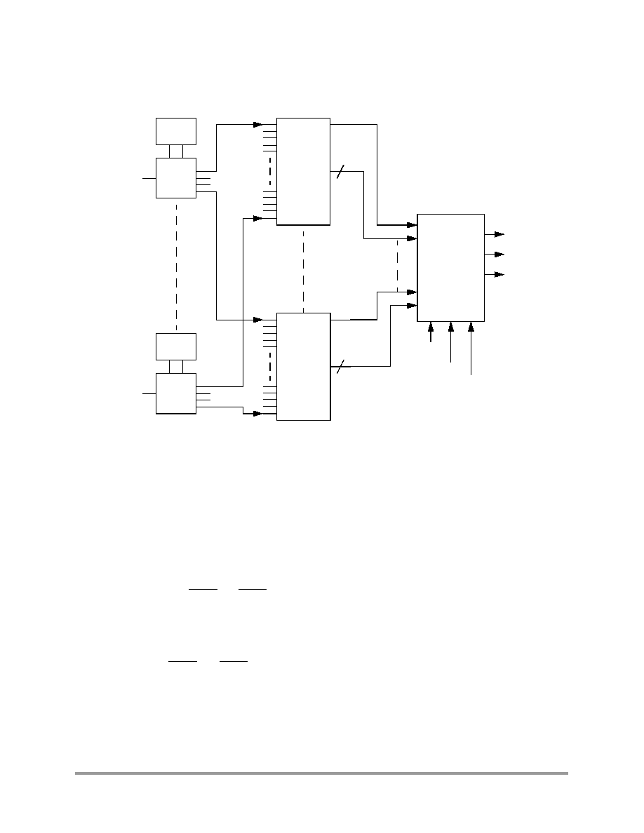
70
56F8346 Technical Data
Preliminary
5.4 Block Diagram
Figure 5-1 Interrupt Controller Block Diagram
5.5 Operating Modes
The ITCN module design contains two major modes of operation:
·
Functional Mode
The ITCN is in this mode by default.
·
Wait and Stop Modes
During Wait and Stop modes, the system clocks and the 56800E core are turned off. The ITCN will
signal a pending IRQ to the System Integration Module (SIM) to restart the clocks and service the
IRQ. An IRQ can only wake up the core if the IRQ is enabled prior to entering the Wait or Stop
mode. Also, the IRQA and IRQB signals automatically become low-level sensitive in these modes
even if the control register bits are set to make them falling-edge sensitive. This is because there is
no clock available to detect the falling edge.
A peripheral which requires a clock to generate interrupts will not be able to generate interrupts
during Stop mode. The FlexCAN module can wake the device from Stop mode, and a reset will do
just that, or IRQA and IRQB can wake it up.
Priority
Level
2 -> 4
Decode
INT1
Priority
Level
2 -> 4
Decode
INT82
Level 0
82 -> 7
Priority
Encoder
any0
Level 3
82 -> 7
Priority
Encoder
any3
INT
VAB
IPIC
CONTROL
7
7
PIC_EN
IACK
SR[9:8]
F
r
e
e
s
c
a
l
e
S
e
m
i
c
o
n
d
u
c
t
o
r
,
I
Freescale Semiconductor, Inc.
For More Information On This Product,
Go to: www.freescale.com
n
c
.
.
.

Register Descriptions
56F8346 Technical Data
71
Preliminary
5.6 Register Descriptions
A register address is the sum of a base address and an address offset. The base address is defined
at the system level and the address offset is defined at the module level. The ITCN peripheral has
24 registers.
Table 5-3 ITCN Register Summary
(ITCN_BASE = $00F1A0)
Register
Acronym
Base Address +
Register Name
Section Location
IPR0
$0
Interrupt Priority Register 0
5.6.1
IPR1
$1
Interrupt Priority Register 1
5.6.2
IPR2
$2
Interrupt Priority Register 2
5.6.3
IPR3
$3
Interrupt Priority Register 3
5.6.4
IPR4
$4
Interrupt Priority Register 4
5.6.5
IPR5
$5
Interrupt Priority Register 5
5.6.6
IPR6
$6
Interrupt Priority Register 6
5.6.7
IPR7
$7
Interrupt Priority Register 7
5.6.8
IPR8
$8
Interrupt Priority Register 8
5.6.9
IPR9
$9
Interrupt Priority Register 9
5.6.10
VBA
$A
Vector Base Address Register
5.6.11
FIM0
$B
Fast Interrupt 0 Match Register
5.6.12
FIVAL0
$C
Fast Interrupt 0 Vector Address Low Register
5.6.13
FIVAH0
$D
Fast Interrupt 0 Vector Address High Register
5.6.14
FIM1
$E
Fast Interrupt 1 Match Register
5.6.15
FIVAL1
$F
Fast Interrupt 1 Vector Address Low Register
5.6.16
FIVAH1
$10
Fast Interrupt 1 Vector Address High Register
5.6.17
IRQP0
$11
IRQ Pending Register 0
5.6.18
IRQP1
$12
IRQ Pending Register 1
5.6.19
IRQP2
$13
IRQ Pending Register 2
5.6.20
IRQP3
$14
IRQ Pending Register 3
5.6.21
IRQP4
$15
IRQ Pending Register 4
5.6.22
IRQP5
$16
IRQ Pending Register 5
5.6.23
Reserved
$17
ICTL
$1D
Interrupt Control Register
5.6.30
F
r
e
e
s
c
a
l
e
S
e
m
i
c
o
n
d
u
c
t
o
r
,
I
Freescale Semiconductor, Inc.
For More Information On This Product,
Go to: www.freescale.com
n
c
.
.
.
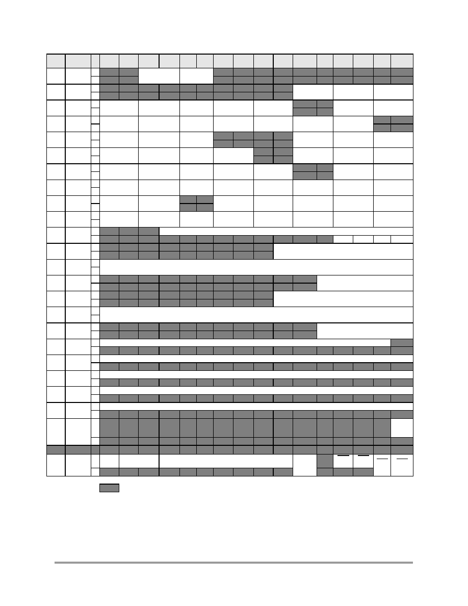
72
56F8346 Technical Data
Preliminary
Add.
Offset
Register
Name
15
14
13
12
11
10
9
8
7
6
5
4
3
2
1
0
$0
IPR0
R
0
0
BKPT_U0 IPL
STPCNT IPL
0
0
0
0
0
0
0
0
0
0
W
$1
IPR1
R
0
0
0
0
0
0
0
0
0
0
RX_REG IPL
TX_REG IPL
TRBUF IPL
W
$2
IPR2
R
FMCBE IPL
FMCC IPL
FMERR IPL
LOCK IPL
LVI IPL
0
0
IRQB IPL
IRQA IPL
W
$3
IPR3
R
GPIOD
IPL
GPIOE
IPL
GPIOF
IPL
FCMSGBUF IPL
FCWKUP IPL
FCERR IPL
FCBOFF IPL
0
0
W
$4
IPR4
R
SPI0_RCV IPL
SPI1_XMIT IPL
SPI1_RCV
IPL
0
0
0
0
GPIOA
IPL
GPIOB
IPL
GPIOC
IPL
W
$5
IPR5
R
DEC1_XIRQ IPL DEC1_HIRQ IPL
SCI1_RCV
IPL
SCI1_RERR IPL
0
0
SCI1_TIDL IPL
SCI1_XMIT IPL
SPI0_XMIT IPL
W
$6
IPR6
R
TMRC0 IPL
TMRD3 IPL
TMRD2 IPL
TMRD1 IPL
TMRD0 IPL
0
0
DEC0_XIRQ IPL DEC0_HIRQ IPL
W
$7
IPR7
R
TMRA0 IPL
TMRB3 IPL
TMRB2 IPL
TMRB1 IPL
TMRB0 IPL
TMRC3 IPL
TMRC2 IPL
TMRC1 IPL
W
$8
IPR8
R
SCI0_RCV IPL
SCI0_RERR IPL
0
0
SCI0_TIDL IPL
SCI0_XMIT IPL
TMRA3 IPL
TMRA2 IPL
TMRA1 IPL
W
0
0
$9
IPR9
R
PWMA F IPL
PWMB F IPL
PWMA_RL
IPL
PWMB_RL IPL
ADCA_ZC IPL
ABCB_ZC IPL
ADCA_CC IPL
ADCB_CC IPL
W
$A
VBA
R
0
0
0
VECTOR BASE ADDRESS
W
$B
VBA0
R
0
0
0
0
0
0
0
0
0
FAST INTERRUPT 0
W
$C
FIVAL0
R
FAST INTERRUPT 0 VECTOR ADDRESS LOW
W
$D
FIVAH0
R
0
0
0
0
0
0
0
0
0
0
0
FAST INTERRUPT 0
VECTOR ADDRESS HIGH
W
$E
FIM1
R
0
0
0
0
0
0
0
0
0
FAST INTERRUPT 1
W
0
0
0
0
0
0
0
0
0
$F
FIVAL1
R
FAST INTERRUPT 1
VECTOR ADDRESS LOW
W
$10
FIVAH1
R
0
0
0
0
0
0
0
0
0
0
0
FAST INTERRUPT 1
VECTOR ADDRESS HIGH
W
0
0
0
0
0
0
0
0
0
0
0
$11
IRQP0
R
PENDING [16:2]
1
W
$12
IRQP1
R
PENDING [32:17]
W
$13
IRQP2
R
PENDING [48:33]
W
$14
IRQP3
R
PENDING [64:49]
W
$15
IRQP4
R
PENDING [80:65]
W
$16
IRQP5
R
1
1
1
1
1
1
1
1
1
1
1
1
1
1
1
PEND-
ING
[81]
W
Reserved
$1D
ICTL
R
INT
IPIC
VAB
INT_DIS
1
IRQB
STATE
IRQA
STATE
IRQB
EDG
IRQA
EDG
W
= Reserved
Figure 5-2 ITCN Register Map Summary
F
r
e
e
s
c
a
l
e
S
e
m
i
c
o
n
d
u
c
t
o
r
,
I
Freescale Semiconductor, Inc.
For More Information On This Product,
Go to: www.freescale.com
n
c
.
.
.

Register Descriptions
56F8346 Technical Data
73
Preliminary
5.6.1
Interrupt Priority Register 0 (IPR0)
Figure 5-3 Interrupt Priority Register 0 (IPR0)
5.6.1.1
Reserved--Bits 1514
This bit field is reserved or not implemented. It is read as 0 and cannot be modified by writing.
5.6.1.2
EOnCE Breakpoint Unit 0 Interrupt Priority Level (BKPT_U0 IPL)--
Bits1312
This field is used to set the interrupt priority levels for IRQs. This IRQ is limited to priorities 1
through 3. It is disabled by default.
·
00 = IRQ disabled (default)
·
01 = IRQ is priority level 1
·
10 = IRQ is priority level 2
·
11 = IRQ is priority level 3
5.6.1.3
EOnCE Step Counter Interrupt Priority Level (STPCNT IPL)--
Bits 1110
This field is used to set the interrupt priority level for IRQs. This IRQ is limited to priorities 1
through 3. It is disabled by default.
·
00 = IRQ disabled (default)
·
01 = IRQ is priority level 1
·
10 = IRQ is priority level 2
·
11 = IRQ is priority level 3
5.6.1.4
Reserved--Bits 90
This bit field is reserved or not implemented. It is read as 0 and cannot be modified by writing.
5.6.2
Interrupt Priority Register 1 (IPR1)
Figure 5-4 Interrupt Priority Register 1 (IPR1)
5.6.2.1
Reserved--Bits 156
This bit field is reserved or not implemented. It is read as 0 and cannot be modified by writing.
Base + $0
15
14
13
12
11
10
9
8
7
6
5
4
3
2
1
0
Read
0
0
BKPT_U0 IPL
STPCNT IPL
0
0
0
0
0
0
0
0
0
0
Write
RESET
0
0
0
0
0
0
0
0
0
0
0
0
0
0
0
0
Base + $1
15
14
13
12
11
10
9
8
7
6
5
4
3
2
1
0
Read
0
0
0
0
0
0
0
0
0
0
RX_REG IPL
TX_REG IPL
TRBUF IPL
Write
RESET
0
0
0
0
0
0
0
0
0
0
0
0
0
0
0
0
F
r
e
e
s
c
a
l
e
S
e
m
i
c
o
n
d
u
c
t
o
r
,
I
Freescale Semiconductor, Inc.
For More Information On This Product,
Go to: www.freescale.com
n
c
.
.
.

74
56F8346 Technical Data
Preliminary
5.6.2.2
EOnCE Receive Register Full Interrupt Priority Level
(RX_REG IPL)--Bits 54
This field is used to set the interrupt priority level for IRQs. This IRQ is limited to priorities 1
through 3. It is disabled by default.
·
00 = IRQ disabled (default)
·
01 = IRQ is priority level 1
·
10 = IRQ is priority level 2
·
11 = IRQ is priority level 3
5.6.2.3
EOnCE Transmit Register Empty Interrupt Priority Level
(TX_REG IPL)--Bits 32
This field is used to set the interrupt priority level for IRQs. This IRQ is limited to priorities 1
through 3. It is disabled by default.
·
00 = IRQ disabled (default)
·
01 = IRQ is priority level 1
·
10 = IRQ is priority level 2
·
11 = IRQ is priority level 3
5.6.2.4
EOnCE Trace Buffer Interrupt Priority Level (TRBUF IPL)--
Bits 10
This field is used to set the interrupt priority level for IRQs. This IRQ is limited to priorities 1
through 3. It is disabled by default.
·
00 = IRQ disabled (default)
·
01 = IRQ is priority level 1
·
10 = IRQ is priority level 2
·
11 = IRQ is priority level 3
5.6.3
Interrupt Priority Register 2 (IPR2)
Figure 5-5 Interrupt Priority Register 2 (IPR2)
Base + $2
15
14
13
12
11
10
9
8
7
6
5
4
3
2
1
0
Read
FMCBE IPL
FMCC IPL
FMERR IPL
LOCK IPL
LVI IPL
0
0
IRQB IPL
IRQA IPL
Write
RESET
0
0
0
0
0
0
0
0
0
0
0
0
0
0
0
0
F
r
e
e
s
c
a
l
e
S
e
m
i
c
o
n
d
u
c
t
o
r
,
I
Freescale Semiconductor, Inc.
For More Information On This Product,
Go to: www.freescale.com
n
c
.
.
.

Register Descriptions
56F8346 Technical Data
75
Preliminary
5.6.3.1
Flash Memory Command, Data, Address Buffers Empty Interrupt
Priority Level (FMCBE IPL)--Bits 1514
This field is used to set the interrupt priority level for IRQs. This IRQ is limited to priorities 0
through 2. It is disabled by default.
·
00 = IRQ disabled (default)
·
01 = IRQ is priority level 0
·
10 = IRQ is priority level 1
·
11 = IRQ is priority level 2
5.6.3.2
Flash Memory Command Complete Priority Level
(FMCC IPL)--Bits 1312
This field is used to set the interrupt priority level for IRQs. This IRQ is limited to priorities 0
through 2. It is disabled by default.
·
00 = IRQ disabled (default)
·
01 = IRQ is priority level 0
·
10 = IRQ is priority level 1
·
11 = IRQ is priority level 2
5.6.3.3
Flash Memory Error Interrupt Priority Level
(FMERR IPL)--Bits 1110
This field is used to set the interrupt priority level for IRQs. This IRQ is limited to priorities 0
through 2. It is disabled by default.
·
00 = IRQ disabled (default)
·
01 = IRQ is priority level 0
·
10 = IRQ is priority level 1
·
11 = IRQ is priority level 2
5.6.3.4
PLL Loss of Lock Interrupt Priority Level (LOCK IPL)--Bits 98
This field is used to set the interrupt priority level for IRQs. This IRQ is limited to priorities 0
through 2. It is disabled by default.
·
00 = IRQ disabled (default)
·
01 = IRQ is priority level 0
·
10 = IRQ is priority level 1
·
11 = IRQ is priority level 2
F
r
e
e
s
c
a
l
e
S
e
m
i
c
o
n
d
u
c
t
o
r
,
I
Freescale Semiconductor, Inc.
For More Information On This Product,
Go to: www.freescale.com
n
c
.
.
.

76
56F8346 Technical Data
Preliminary
5.6.3.5
Low Voltage Detector Interrupt Priority Level (LVI IPL)--Bits 76
This field is used to set the interrupt priority level for IRQs. This IRQ is limited to priorities 0
through 2. It is disabled by default.
·
00 = IRQ disabled (default)
·
01 = IRQ is priority level 0
·
10 = IRQ is priority level 1
·
11 = IRQ is priority level 2
5.6.3.6
Reserved--Bits 54
This bit field is reserved or not implemented. It is read as 0 and cannot be modified by writing.
5.6.3.7
External IRQ B Interrupt Priority Level (IRQB IPL)--Bits 32
This field is used to set the interrupt priority level for IRQs. This IRQ is limited to priorities 0
through 2. It is disabled by default.
·
00 = IRQ disabled (default)
·
01 = IRQ is priority level 0
·
10 = IRQ is priority level 1
·
11 = IRQ is priority level 2
5.6.3.8
External IRQ A Interrupt Priority Level (IRQA IPL)--Bits 10
This field is used to set the interrupt priority level for IRQs. This IRQ is limited to priorities 0
through 2. It is disabled by default.
·
00 = IRQ disabled (default)
·
01 = IRQ is priority level 0
·
10 = IRQ is priority level 1
·
11 = IRQ is priority level 2
5.6.4
Interrupt Priority Register 3 (IPR3)
Figure 5-6 Interrupt Priority Register 3 (IPR3)
5.6.4.1
GPIO D Interrupt Priority Level (GPIOD IPL)--Bits 1514
This field is used to set the interrupt priority level for IRQs. This IRQ is limited to priorities 0
through 2. They are disabled by default.
·
00 = IRQ disabled (default)
·
01 = IRQ is priority level 0
·
10 = IRQ is priority level 1
·
11 = IRQ is priority level 2
Base + $3
15
14
13
12
11
10
9
8
7
6
5
4
3
2
1
0
Read
GPIODIPL
GPIOE IPL
GPIOFIPL
FCMSGBUF IPL
FCWKUP IPL
FCERR IPL
FCBOFF IPL
0
0
Write
RESET
0
0
0
0
0
0
0
0
0
0
0
0
0
0
0
0
F
r
e
e
s
c
a
l
e
S
e
m
i
c
o
n
d
u
c
t
o
r
,
I
Freescale Semiconductor, Inc.
For More Information On This Product,
Go to: www.freescale.com
n
c
.
.
.

Register Descriptions
56F8346 Technical Data
77
Preliminary
5.6.4.2
GPIO E Interrupt Priority Level (GPIOE IPL)--Bits 1312
This field is used to set the interrupt priority level for IRQs. This IRQ is limited to priorities 0
through 2. They are disabled by default.
·
00 = IRQ disabled (default)
·
01 = IRQ is priority level 0
·
10 = IRQ is priority level 1
·
11 = IRQ is priority level 2
5.6.4.3
GPIO F Interrupt Priority Level (GPIOF IPL)--Bits 1110
This field is used to set the interrupt priority level for IRQs. This IRQ is limited to priorities 0
through 2two. They are disabled by default.
·
00 = IRQ disabled (default)
·
01 = IRQ is priority level 0
·
10 = IRQ is priority level 1
·
11 = IRQ is priority level 2
5.6.4.4
FlexCAN Message Buffer Interrupt Priority Level
(FCMSGBUF IPL)--Bits 98
This field is used to set the interrupt priority level for IRQs. This IRQ is limited to priorities 0
through 2. They are disabled by default.
·
00 = IRQ disabled (default)
·
01 = IRQ is priority level 0
·
10 = IRQ is priority level 1
·
11 = IRQ is priority level 2
5.6.4.5
FlexCAN Wake Up Interrupt Priority Level (FCWKUP IPL)--
Bits 76
This field is used to set the interrupt priority level for IRQs. This IRQ is limited to priorities 0
through 2. They are disabled by default.
·
00 = IRQ disabled (default)
·
01 = IRQ is priority level 0
·
10 = IRQ is priority level 1
·
11 = IRQ is priority level 2
5.6.4.6
FlexCAN Error Interrupt Priority Level (FCERR IPL)-- Bits 54
This field is used to set the interrupt priority level for IRQs. This IRQ is limited to priorities 0
through 2. They are disabled by default.
·
00 = IRQ disabled (default)
·
01 = IRQ is priority level 0
·
10 = IRQ is priority level 1
·
11 = IRQ is priority level 2
F
r
e
e
s
c
a
l
e
S
e
m
i
c
o
n
d
u
c
t
o
r
,
I
Freescale Semiconductor, Inc.
For More Information On This Product,
Go to: www.freescale.com
n
c
.
.
.

78
56F8346 Technical Data
Preliminary
5.6.4.7
FlexCAN Bus Off Interrupt Priority Level (FCBOFF IPL)-- Bits 32
This field is used to set the interrupt priority level for IRQs. This IRQ is limited to priorities 0
through 2. They are disabled by default.
·
00 = IRQ disabled (default)
·
01 = IRQ is priority level 0
·
10 = IRQ is priority level 1
·
11 = IRQ is priority level 2
5.6.4.8
Reserved--Bits 10
This bit field is reserved or not implemented. It is read as 0 and cannot be modified by writing.
5.6.5
Interrupt Priority Register 4 (IPR4)
Figure 5-7 Interrupt Priority Register 4 (IPR4)
5.6.5.1
SPI0 Receiver Full Interrupt Priority Level (SPI0_RCV IPL)--
Bits 1514
This field is used to set the interrupt priority level for IRQs. This IRQ is limited to priorities 0
through 2. They are disabled by default.
·
00 = IRQ disabled (default)
·
01 = IRQ is priority level 0
·
10 = IRQ is priority level 1
·
11 = IRQ is priority level 2
5.6.5.2
SPI1 Transmit Empty Interrupt Priority Level (SPI1_XMIT IPL)--
Bits 1312
This field is used to set the interrupt priority level for IRQs. This IRQ is limited to priorities 0
through 2. They are disabled by default.
·
00 = IRQ disabled (default)
·
01 = IRQ is priority level 0
·
10 = IRQ is priority level 1
·
11 = IRQ is priority level 2
Base + $4
15
14
13
12
11
10
9
8
7
6
5
4
3
2
1
0
Read
SPI0_RCV
IPL
SPI1_XMIT
IPL
SPI1_RCV
IPL
0
0
0
0
GPIOA IPL
GPIOB IPL
GPIOC IPL
Write
RESET
0
0
0
0
0
0
0
0
0
0
0
0
0
0
0
0
F
r
e
e
s
c
a
l
e
S
e
m
i
c
o
n
d
u
c
t
o
r
,
I
Freescale Semiconductor, Inc.
For More Information On This Product,
Go to: www.freescale.com
n
c
.
.
.

Register Descriptions
56F8346 Technical Data
79
Preliminary
5.6.5.3
SPI1 Receiver Full Interrupt Priority Level (SPI1_RCV IPL)--
Bits 1110
This field is used to set the interrupt priority level for IRQs. This IRQ is limited to priorities 0
through 2. They are disabled by default.
·
00 = IRQ disabled (default)
·
01 = IRQ is priority level 0
·
10 = IRQ is priority level 1
·
11 = IRQ is priority level 2
5.6.5.4
Reserved--Bits 96
This bit field is reserved or not implemented. It is read as 0 and cannot be modified by writing.
5.6.5.5
GPIO A Interrupt Priority Level (GPIOA IPL)--Bits 54
This field is used to set the interrupt priority level for IRQs. This IRQ is limited to priorities 0
through 2. They are disabled by default.
·
00 = IRQ disabled (default)
·
01 = IRQ is priority level 0
·
10 = IRQ is priority level 1
·
11 = IRQ is priority level 2
5.6.5.6
GPIO B Interrupt Priority Level (GPIOB IPL)--Bits 32
This field is used to set the interrupt priority level for IRQs. This IRQ is limited to priorities 0
through 2. They are disabled by default.
·
00 = IRQ disabled (default)
·
01 = IRQ is priority level 0
·
10 = IRQ is priority level 1
·
11 = IRQ is priority level 2
5.6.5.7
GPIO C Interrupt Priority Level (GPIOC IPL)--Bits 10
This field is used to set the interrupt priority level for IRQs. This IRQ is limited to priorities 0
through 2. They are disabled by default.
·
00 = IRQ disabled (default)
·
01 = IRQ is priority level 0
·
10 = IRQ is priority level 1
·
11 = IRQ is priority level 2
F
r
e
e
s
c
a
l
e
S
e
m
i
c
o
n
d
u
c
t
o
r
,
I
Freescale Semiconductor, Inc.
For More Information On This Product,
Go to: www.freescale.com
n
c
.
.
.

80
56F8346 Technical Data
Preliminary
5.6.6
Interrupt Priority Register 5 (IPR5)
Figure 5-8 Interrupt Priority Register 5 (IPR5)
5.6.6.1
Quadrature Decoder 1 INDEX Pulse Interrupt Priority Level
(DEC1_XIRQ IPL)--Bits 1514
This field is used to set the interrupt priority level for IRQs. This IRQ is limited to priorities 0
through 2. They are disabled by default.
·
00 = IRQ disabled (default)
·
01 = IRQ is priority level 0
·
10 = IRQ is priority level 1
·
11 = IRQ is priority level 2
5.6.6.2
Quadrature Decoder 1 HOME Signal Transition or Watchdog Timer
Interrupt Priority Level (DEC1_HIRQ IPL)--Bits 1312
This field is used to set the interrupt priority level for IRQs. This IRQ is limited to priorities 0
through 2. They are disabled by default.
·
00 = IRQ disabled (default)
·
01 = IRQ is priority level 0
·
10 = IRQ is priority level 1
·
11 = IRQ is priority level 2
5.6.6.3
SCI 1 Receiver Full Interrupt Priority Level (SCI1_RCV IPL)--
Bits 1110
This field is used to set the interrupt priority level for IRQs. This IRQ is limited to priorities 0
through 2. They are disabled by default.
·
00 = IRQ disabled (default)
·
01 = IRQ is priority level 0
·
10 = IRQ is priority level 1
·
11 = IRQ is priority level 2
Base + $5
15
14
13
12
11
10
9
8
7
6
5
4
3
2
1
0
Read
DEC1_XIRQ
IPL
DEC1_HIRQ
IPL
SCI1_RCV
IPL
SCI1_RERR
IPL
0
0
SCI1_TIDL
IPL
SCI1_XMIT
IPL
SPI0_XMIT
IPL
Write
RESET
0
0
0
0
0
0
0
0
0
0
0
0
0
0
0
0
F
r
e
e
s
c
a
l
e
S
e
m
i
c
o
n
d
u
c
t
o
r
,
I
Freescale Semiconductor, Inc.
For More Information On This Product,
Go to: www.freescale.com
n
c
.
.
.

Register Descriptions
56F8346 Technical Data
81
Preliminary
5.6.6.4
SCI 1 Receiver Error Interrupt Priority Level (SCI1_RERR IPL)--
Bits 98
This field is used to set the interrupt priority level for IRQs. This IRQ is limited to priorities 0
through 2. They are disabled by default.
·
00 = IRQ disabled (default)
·
01 = IRQ is priority level 0
·
10 = IRQ is priority level 1
·
11 = IRQ is priority level 2
5.6.6.5
Reserved--Bits 76
This bit field is reserved or not implemented. It is read as 0 and cannot be modified by writing.
5.6.6.6
SCI 1 Transmitter Idle Interrupt Priority Level (SCI1_TIDL IPL)--
Bits 54
This field is used to set the interrupt priority level for IRQs. This IRQ is limited to priorities 0
through 2. They are disabled by default.
·
00 = IRQ disabled (default)
·
01 = IRQ is priority level 0
·
10 = IRQ is priority level 1
·
11 = IRQ is priority level 2
5.6.6.7
SCI 1 Transmitter Empty Interrupt Priority Level (SCI1_XMIT IPL)--
Bits 32
This field is used to set the interrupt priority level for IRQs. This IRQ is limited to priorities 0
through 2. They are disabled by default.
·
00 = IRQ disabled (default)
·
01 = IRQ is priority level 0
·
10 = IRQ is priority level 1
·
11 = IRQ is priority level 2
5.6.6.8
SPI 0 Transmitter Empty Interrupt Priority Level (SPI0_XMIT IPL)--
Bits 10
This field is used to set the interrupt priority level for IRQs. This IRQ is limited to priorities 0
through 2. They are disabled by default.
·
00 = IRQ disabled (default)
·
01 = IRQ is priority level 0
·
10 = IRQ is priority level 1
·
11 = IRQ is priority level 2
F
r
e
e
s
c
a
l
e
S
e
m
i
c
o
n
d
u
c
t
o
r
,
I
Freescale Semiconductor, Inc.
For More Information On This Product,
Go to: www.freescale.com
n
c
.
.
.

82
56F8346 Technical Data
Preliminary
5.6.7
Interrupt Priority Register 6 (IPR6)
Figure 5-9 Interrupt Priority Register 6 (IPR6)
5.6.7.1
Timer C, Channel 0 Interrupt Priority Level (TMRC0 IPL)--
Bits 1514
This field is used to set the interrupt priority level for IRQs. This IRQ is limited to priorities 0
through 2. They are disabled by default.
·
00 = IRQ disabled (default)
·
01 = IRQ is priority level 0
·
10 = IRQ is priority level 1
·
11 = IRQ is priority level 2
5.6.7.2
Timer D, Channel 3 Interrupt Priority Level (TMRD3 IPL)--
Bits 1312
This field is used to set the interrupt priority level for IRQs. This IRQ is limited to priorities 0
through 2. They are disabled by default.
·
00 = IRQ disabled (default)
·
01 = IRQ is priority level 0
·
10 = IRQ is priority level 1
·
11 = IRQ is priority level 2
5.6.7.3
Timer D, Channel 2 Interrupt Priority Level (TMRD2 IPL)--
Bits 1110
This field is used to set the interrupt priority level for IRQs. This IRQ is limited to priorities 0
through 2. They are disabled by default.
·
00 = IRQ disabled (default)
·
01 = IRQ is priority level 0
·
10 = IRQ is priority level 1
·
11 = IRQ is priority level 2
Base + $6
15
14
13
12
11
10
9
8
7
6
5
4
3
2
1
0
Read
TMRC0 IPL
TMRD3 IPL
TMRD2 IPL
TMRD1 IPL
TMRD0 IPL
0
0
DEC0_XIRQ
IPL
DEC0_HIRQ
IPL
Write
RESET
0
0
0
0
0
0
0
0
0
0
0
0
0
0
0
0
F
r
e
e
s
c
a
l
e
S
e
m
i
c
o
n
d
u
c
t
o
r
,
I
Freescale Semiconductor, Inc.
For More Information On This Product,
Go to: www.freescale.com
n
c
.
.
.

Register Descriptions
56F8346 Technical Data
83
Preliminary
5.6.7.4
Timer D, Channel 1 Interrupt Priority Level (TMRD1 IPL)--
Bits 98
This field is used to set the interrupt priority level for IRQs. This IRQ is limited to priorities 0
through 2. They are disabled by default.
·
00 = IRQ disabled (default)
·
01 = IRQ is priority level 0
·
10 = IRQ is priority level 1
·
11 = IRQ is priority level 2
5.6.7.5
Timer D, Channel 0 Interrupt Priority Level (TMRD0 IPL)--
Bits 76
This field is used to set the interrupt priority level for IRQs. This IRQ is limited to priorities 0
through 2. They are disabled by default.
·
00 = IRQ disabled (default)
·
01 = IRQ is priority level 0
·
10 = IRQ is priority level 1
·
11 = IRQ is priority level 2
5.6.7.6
Reserved--Bits 54
This bit field is reserved or not implemented. It is read as 0 and cannot be modified by writing.
5.6.7.7
Quadrature Decoder 0, INDEX Pulse Interrupt Priority Level
(DEC0_XIRQ IPL)--Bits 32
This field is used to set the interrupt priority level for IRQs. This IRQ is limited to priorities 0
through 2. They are disabled by default.
·
00 = IRQ disabled (default)
·
01 = IRQ is priority level 0
·
10 = IRQ is priority level 1
·
11 = IRQ is priority level 2
5.6.7.8
Quadrature Decoder 0, HOME Signal Transition or Watchdog
Timer Interrupt Priority Level (DEC0_HIRQ IPL)--Bits 10
This field is used to set the interrupt priority level for IRQs. This IRQ is limited to priorities 0
through 2. They are disabled by default.
·
00 = IRQ disabled (default)
·
01 = IRQ is priority level 0
·
10 = IRQ is priority level 1
·
11 = IRQ is priority level 2
F
r
e
e
s
c
a
l
e
S
e
m
i
c
o
n
d
u
c
t
o
r
,
I
Freescale Semiconductor, Inc.
For More Information On This Product,
Go to: www.freescale.com
n
c
.
.
.

84
56F8346 Technical Data
Preliminary
5.6.8
Interrupt Priority Register 7 (IPR7)
Figure 5-10 Interrupt Priority Register (IPR7)
5.6.8.1
Timer A, Channel 0 Interrupt Priority Level (TMRA0 IPL)--
Bits 1514
This field is used to set the interrupt priority level for IRQs. This IRQ is limited to priorities 0
through 2. They are disabled by default.
·
00 = IRQ disabled (default)
·
01 = IRQ is priority level 0
·
10 = IRQ is priority level 1
·
11 = IRQ is priority level 2
5.6.8.2
Timer B, Channel 3 Interrupt Priority Level (TMRB3 IPL)--
Bits 1312
This field is used to set the interrupt priority level for IRQs. This IRQ is limited to priorities 0
through 2. They are disabled by default.
·
00 = IRQ disabled (default)
·
01 = IRQ is priority level 0
·
10 = IRQ is priority level 1
·
11 = IRQ is priority level 2
5.6.8.3
Timer B, Channel 2 Interrupt Priority Level (TMRB2 IPL)--
Bits 1110
This field is used to set the interrupt priority level for IRQs. This IRQ is limited to priorities 0
through 2. They are disabled by default.
·
00 = IRQ disabled (default)
·
01 = IRQ is priority level 0
·
10 = IRQ is priority level 1
·
11 = IRQ is priority level 2
Base + $7
15
14
13
12
11
10
9
8
7
6
5
4
3
2
1
0
Read
TMRA0 IPL
TMRB3 IPL
TMRB2 IPL
TMRB1 IPL
TMRB0 IPL
TMRC3 IPL
TMRC2 IPL
TMRC1 IPL
Write
RESET
0
0
0
0
0
0
0
0
0
0
0
0
0
0
0
0
F
r
e
e
s
c
a
l
e
S
e
m
i
c
o
n
d
u
c
t
o
r
,
I
Freescale Semiconductor, Inc.
For More Information On This Product,
Go to: www.freescale.com
n
c
.
.
.

Register Descriptions
56F8346 Technical Data
85
Preliminary
5.6.8.4
Timer B, Channel 1 Interrupt Priority Level (TMRB1 IPL)--Bits 98
This field is used to set the interrupt priority level for IRQs. This IRQ is limited to priorities 0
through 2. They are disabled by default.
·
00 = IRQ disabled (default)
·
01 = IRQ is priority level 0
·
10 = IRQ is priority level 1
·
11 = IRQ is priority level 2
5.6.8.5
Timer B, Channel 0 Interrupt Priority Level (TMRB0 IPL)--Bits 76
This field is used to set the interrupt priority level for IRQs. This IRQ is limited to priorities 0
through 2. They are disabled by default.
·
00 = IRQ disabled (default)
·
01 = IRQ is priority level 0
·
10 = IRQ is priority level 1
·
11 = IRQ is priority level 2
5.6.8.6
Timer C, Channel 3 Interrupt Priority Level (TMRC3 IPL)--Bits 54
This field is used to set the interrupt priority level for IRQs. This IRQ is limited to priorities 0
through 2. They are disabled by default.
·
00 = IRQ disabled (default)
·
01 = IRQ is priority level 0
·
10 = IRQ is priority level 1
·
11 = IRQ is priority level 2
5.6.8.7
Timer C, Channel 2 Interrupt Priority Level (TMRC2 IPL)--Bits 32
This field is used to set the interrupt priority level for IRQs. This IRQ is limited to priorities 0
through 2. They are disabled by default.
·
00 = IRQ disabled (default)
·
01 = IRQ is priority level 0
·
10 = IRQ is priority level 1
·
11 = IRQ is priority level 2
5.6.8.8
Timer C, Channel 1 Interrupt Priority Level (TMRC1 IPL)--Bits 10
This field is used to set the interrupt priority level for IRQs. This IRQ is limited to priorities 0
through 2. They are disabled by default.
·
00 = IRQ disabled (default)
·
01 = IRQ is priority level 0
·
10 = IRQ is priority level 1
·
11 = IRQ is priority level 2
F
r
e
e
s
c
a
l
e
S
e
m
i
c
o
n
d
u
c
t
o
r
,
I
Freescale Semiconductor, Inc.
For More Information On This Product,
Go to: www.freescale.com
n
c
.
.
.

86
56F8346 Technical Data
Preliminary
5.6.9
Interrupt Priority Register 8 (IPR8)
Figure 5-11 Interrupt Priority Register 8 (IPR8)
5.6.9.1
SCI0 Receiver Full Interrupt Priority Level (SCI0_RCV IPL)--
Bits 1514
This field is used to set the interrupt priority level for IRQs. This IRQ is limited to priorities 0
through 2. They are disabled by default.
·
00 = IRQ disabled (default)
·
01 = IRQ is priority level 0
·
10 = IRQ is priority level 1
·
11 = IRQ is priority level 2
5.6.9.2
SCI0 Receiver Error Interrupt Priority Level (SCI0_RERR IPL)--
Bits 1312
This field is used to set the interrupt priority level for IRQs. This IRQ is limited to priorities 0
through 2. They are disabled by default.
·
00 = IRQ disabled (default)
·
01 = IRQ is priority level 0
·
10 = IRQ is priority level 1
·
11 = IRQ is priority level 2
5.6.9.3
Reserved--Bits 1110
This bit field is reserved or not implemented. It is read as 0 and cannot be modified by writing.
5.6.9.4
SCI0 Transmitter Idle Interrupt Priority Level (SCI0_TIDL IPL)--
Bits 98
This field is used to set the interrupt priority level for IRQs. This IRQ is limited to priorities 0
through 2. They are disabled by default.
·
00 = IRQ disabled (default)
·
01 = IRQ is priority level 0
·
10 = IRQ is priority level 1
·
11 = IRQ is priority level 2
Base + $8
15
14
13
12
11
10
9
8
7
6
5
4
3
2
1
0
Read
SCI0_RCV
IPL
SCI0_RERR
IPL
0
0
SCI0_TIDL
IPL
SCI0_XMIT
IPL
TMRA3 IPL
TMRA2 IPL
TMRA1 IPL
Write
RESET
0
0
0
0
0
0
0
0
0
0
0
0
0
0
0
0
F
r
e
e
s
c
a
l
e
S
e
m
i
c
o
n
d
u
c
t
o
r
,
I
Freescale Semiconductor, Inc.
For More Information On This Product,
Go to: www.freescale.com
n
c
.
.
.

Register Descriptions
56F8346 Technical Data
87
Preliminary
5.6.9.5
SCI0 Transmitter Empty Interrupt Priority Level (SCI0_XMIT IPL)--
Bits 76
This field is used to set the interrupt priority level for IRQs. This IRQ is limited to priorities 0
through 2. They are disabled by default.
·
00 = IRQ disabled (default)
·
01 = IRQ is priority level 0
·
10 = IRQ is priority level 1
·
11 = IRQ is priority level 2
5.6.9.6
Timer A, Channel 3 Interrupt Priority Level (TMRA3 IPL)--Bits 54
This field is used to set the interrupt priority level for IRQs. This IRQ is limited to priorities 0
through 2. They are disabled by default.
·
00 = IRQ disabled (default)
·
01 = IRQ is priority level 0
·
10 = IRQ is priority level 1
·
11 = IRQ is priority level 2
5.6.9.7
Timer A, Channel 2 Interrupt Priority Level (TMRA2 IPL)--Bits 32
This field is used to set the interrupt priority level for IRQs. This IRQ is limited to priorities 0
through 2. They are disabled by default.
·
00 = IRQ disabled (default)
·
01 = IRQ is priority level 0
·
10 = IRQ is priority level 1
·
11 = IRQ is priority level 2
5.6.9.8
Timer A, Channel 1 Interrupt Priority Level (TMRA1 IPL)--Bits 10
This field is used to set the interrupt priority level for IRQs. This IRQ is limited to priorities 0
through 2. They are disabled by default.
·
00 = IRQ disabled (default)
·
01 = IRQ is priority level 0
·
10 = IRQ is priority level 1
·
11 = IRQ is priority level 2
5.6.10
Interrupt Priority Register 9 (IPR9)
Figure 5-12 Interrupt Priority Register 9 (IPR9)
Base + $9
15
14
13
12
11
10
9
8
7
6
5
4
3
2
1
0
Read
PWMA_F IPL
PWMB_F IPL
PWMA_RL
IPL
PWM_RL IPL
ADCA_ZC IPL ABCB_ZC IPL
ADCA_CC
IPL
ADCB_CC
IPL
Write
RESET
0
0
0
0
0
0
0
0
0
0
0
0
0
0
0
0
F
r
e
e
s
c
a
l
e
S
e
m
i
c
o
n
d
u
c
t
o
r
,
I
Freescale Semiconductor, Inc.
For More Information On This Product,
Go to: www.freescale.com
n
c
.
.
.

88
56F8346 Technical Data
Preliminary
5.6.10.1 PWM A Fault Interrupt Priority Level (PWMA_F IPL)--Bits 1514
This field is used to set the interrupt priority level for IRQs. This IRQ is limited to priorities 0
through 2. They are disabled by default.
·
00 = IRQ disabled (default)
·
01 = IRQ is priority level 0
·
10 = IRQ is priority level 1
·
11 = IRQ is priority level 2
5.6.10.2 PWM B Fault Interrupt Priority Level (PWMB_F IPL)--Bits 1312
This field is used to set the interrupt priority level for IRQs. This IRQ is limited to priorities 0
through 2. They are disabled by default.
·
00 = IRQ disabled (default)
·
01 = IRQ is priority level 0
·
10 = IRQ is priority level 1
·
11 = IRQ is priority level 2
5.6.10.3 Reload PWM A Interrupt Priority Level (PWMA_RL IPL)--
Bits 1110
This field is used to set the interrupt priority level for IRQs. This IRQ is limited to priorities 0
through 2. They are disabled by default.
·
00 = IRQ disabled (default)
·
01 = IRQ is priority level 0
·
10 = IRQ is priority level 1
·
11 = IRQ is priority level 2
5.6.10.4 Reload PWM B Interrupt Priority Level (PWMB_RL IPL)--Bits 98
This field is used to set the interrupt priority level for IRQs. This IRQ is limited to priorities 0
through 2. They are disabled by default.
·
00 = IRQ disabled (default)
·
01 = IRQ is priority level 0
·
10 = IRQ is priority level 1
·
11 = IRQ is priority level 2
5.6.10.5 ADC A Zero Crossing Interrupt Priority Level (ADCA_ZC IPL)--
Bits 76
This field is used to set the interrupt priority level for IRQs. This IRQ is limited to priorities 0
through 2. They are disabled by default.
·
00 = IRQ disabled (default)
·
01 = IRQ is priority level 0
·
10 = IRQ is priority level 1
·
11 = IRQ is priority level 2
F
r
e
e
s
c
a
l
e
S
e
m
i
c
o
n
d
u
c
t
o
r
,
I
Freescale Semiconductor, Inc.
For More Information On This Product,
Go to: www.freescale.com
n
c
.
.
.

Register Descriptions
56F8346 Technical Data
89
Preliminary
5.6.10.6 ADC B Zero Crossing Interrupt Priority Level (ADCB_ZC IPL)--
Bits 54
This field is used to set the interrupt priority level for IRQs. This IRQ is limited to priorities 0
through 2. They are disabled by default.
·
00 = IRQ disabled (default)
·
01 = IRQ is priority level 0
·
10 = IRQ is priority level 1
·
11 = IRQ is priority level 2
5.6.10.7 ADC A Conversion Complete Interrupt Priority Level
(ADCA_CC IPL)--Bits 32
This field is used to set the interrupt priority level for IRQs. This IRQ is limited to priorities 0
through 2. They are disabled by default.
·
00 = IRQ disabled (default)
·
01 = IRQ is priority level 0
·
10 = IRQ is priority level 1
·
11 = IRQ is priority level 2
5.6.10.8 ADC B Conversion Complete Interrupt Priority Level
(ADCB_CC IPL)--Bits 10
This field is used to set the interrupt priority level for IRQs. This IRQ is limited to priorities 0
through 2. They are disabled by default.
·
00 = IRQ disabled (default)
·
01 = IRQ is priority level 0
·
10 = IRQ is priority level 1
·
11 = IRQ is priority level 2
5.6.11
Vector Base Address Register (VBA)
Figure 5-13 Vector Base Address Register (VBA)
5.6.11.1 Reserved--Bits 1513
This bit field is reserved or not implemented. It is read as 0 and cannot be modified by writing.
Base + $A
15
14
13
12
11
10
9
8
7
6
5
4
3
2
1
0
Read
0
0
0
VECTOR BASE ADDRESS
Write
RESET
0
0
0
0
0
0
0
0
0
0
0
0
0
0
0
0
F
r
e
e
s
c
a
l
e
S
e
m
i
c
o
n
d
u
c
t
o
r
,
I
Freescale Semiconductor, Inc.
For More Information On This Product,
Go to: www.freescale.com
n
c
.
.
.
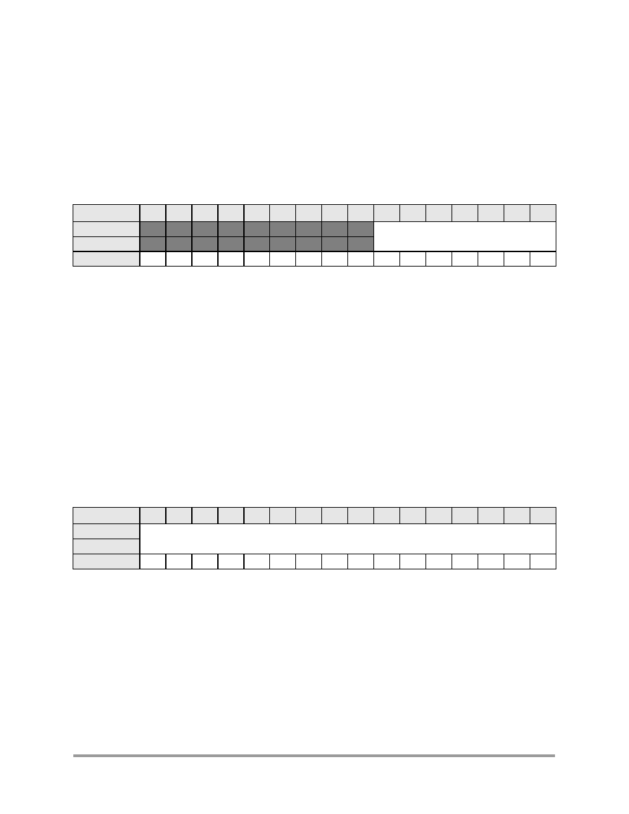
90
56F8346 Technical Data
Preliminary
5.6.11.2 Interrupt Vector Base Address (VECTOR BASE ADDRESS)--
Bits 120
The contents of this register determine the location of the Vector Address Table. The value in this
register is used as the upper 13 bits of the interrupt Vector Address Bus (VAB[20:0]). The lower
eight bits are determined based upon the highest-priority interrupt. They are then appended onto
VBA before presenting the full VAB to the 56800E core; see
Section 5.3.1
for details.
5.6.12
Fast Interrupt 0 Match Register (FIM0)
Figure 5-14 Fast Interrupt 0 Match Register (FIM0)
5.6.12.1 Reserved--Bits 157
This bit field is reserved or not implemented. It is read as 0 and cannot be modified by writing.
5.6.12.2 Fast Interrupt 0 Vector Number (FAST INTERRUPT 0)--Bits 60
This value determines which IRQ will be a Fast Interrupt 0. Fast interrupts vector directly to a
service routine based on values in the Fast Interrupt Vector Address registers without having to go
to a jump table first; see
Section 5.3.3
. IRQs used as fast interrupts must be set to priority level 2.
Unexpected results will occur if a fast interrupt vector is set to any other priority. Fast interrupts
automatically become the highest-priority level 2 interrupt, regardless of their location in the
interrupt table, prior to being declared as fast interrupt. Fast Interrupt 0 has priority over Fast
Interrupt 1. To determine the vector number of each IRQ, refer to
Table 4-5
.
5.6.13
Fast Interrupt 0 Vector Address Low Register (FIVAL0)
Figure 5-15 Fast Interrupt 0 Vector Address Low Register (FIVAL0)
5.6.13.1 Fast Interrupt 0 Vector Address Low (FIVAL0)--Bits 150
The lower 16 bits of the vector address used for Fast Interrupt 0. This register is combined with
FIVAH0 to form the 21-bit vector address for Fast Interrupt 0 defined in the FIM0 register.
Base + $B
15
14
13
12
11
10
9
8
7
6
5
4
3
2
1
0
Read
0
0
0
0
0
0
0
0
0
FAST INTERRUPT 0
Write
RESET
0
0
0
0
0
0
0
0
0
0
0
0
0
0
0
0
Base + $C
15
14
13
12
11
10
9
8
7
6
5
4
3
2
1
0
Read
FAST INTERRUPT 0
VECTOR ADDRESS LOW
Write
RESET
0
0
0
0
0
0
0
0
0
0
0
0
0
0
0
0
F
r
e
e
s
c
a
l
e
S
e
m
i
c
o
n
d
u
c
t
o
r
,
I
Freescale Semiconductor, Inc.
For More Information On This Product,
Go to: www.freescale.com
n
c
.
.
.
Register Descriptions
56F8346 Technical Data
91
Preliminary
5.6.14
Fast Interrupt 0 Vector Address High Register (FIVAH0)
Figure 5-16 Fast Interrupt 0 Vector Address High Register (FIVAH0)
5.6.14.1 Reserved--Bits 155
This bit field is reserved or not implemented. It is read as 0 and cannot be modified by writing.
5.6.14.2 Fast Interrupt 0 Vector Address High (FIVAH0)--Bits 40
The upper five bits of the vector address used for Fast Interrupt 0. This register is combined with
FIVAL0 to form the 21-bit vector address for Fast Interrupt 0 defined in the FIM0 register.
5.6.15
Fast Interrupt 1 Match Register (FIM1)
Figure 5-17 Fast Interrupt 1 Match Register (FIM1)
5.6.15.1 Reserved--Bits 157
This bit field is reserved or not implemented. It is read as 0, but cannot be modified by writing.
5.6.15.2 Fast Interrupt 1 Vector Number (FAST INTERRUPT 1)--Bits 60
This value determines which IRQ will be a Fast Interrupt 1. Fast interrupts vector directly to a
service routine based on values in the Fast Interrupt Vector Address registers without having to go
to a jump table first; see
Section 5.3.3
. IRQs used as fast interrupts must be set to priority level 2.
Unexpected results will occur if a fast interrupt vector is set to any other priority. Fast interrupts
automatically become the highest-priority level 2 interrupt, regardless of their location in the
interrupt table, prior to being declared as fast interrupt. Fast Interrupt 0 has priority over Fast
Interrupt 1. To determine the vector number of each IRQ, refer to
Table 4-5
.
5.6.16
Fast Interrupt 1 Vector Address Low Register (FIVAL1)
Figure 5-18 Fast Interrupt 1 Vector Address Low Register (FIVAL1)
Base + $D
15
14
13
12
11
10
9
8
7
6
5
4
3
2
1
0
Read
0
0
0
0
0
0
0
0
0
0
0
FAST INTERRUPT 0
VECTOR ADDRESS HIGH
Write
RESET
0
0
0
0
0
0
0
0
0
0
0
0
0
0
0
0
Base + $E
15
14
13
12
11
10
9
8
7
6
5
4
3
2
1
0
Read
0
0
0
0
0
0
0
0
0
FAST INTERRUPT 1
Write
RESET
0
0
0
0
0
0
0
0
0
0
0
0
0
0
0
0
Base + $F
15
14
13
12
11
10
9
8
7
6
5
4
3
2
1
0
Read
FAST INTERRUPT 1
VECTOR ADDRESS LOW
Write
RESET
0
0
0
0
0
0
0
0
0
0
0
0
0
0
0
0
F
r
e
e
s
c
a
l
e
S
e
m
i
c
o
n
d
u
c
t
o
r
,
I
Freescale Semiconductor, Inc.
For More Information On This Product,
Go to: www.freescale.com
n
c
.
.
.
92
56F8346 Technical Data
Preliminary
5.6.16.1 Fast Interrupt 1 Vector Address Low (FIVAL1)--Bits 150
The lower 16 bits of vector address are used for Fast Interrupt 1. This register is combined with
FIVAL1 to form the 21-bit vector address for Fast Interrupt 1 defined in the FIM1 register.
5.6.17
Fast Interrupt 1 Vector Address High Register (FIVAH1)
Figure 5-19 Fast Interrupt 1 Vector Address High Register (FIVAH1)
5.6.17.1 Reserved--Bits 155
This bit field is reserved or not implemented. It is read as 0 and cannot be modified by writing.
5.6.17.2 Fast Interrupt 1 Vector Address High (FIVAH1)--Bits 40
The upper five bits of the vector address are used for Fast Interrupt 1. This register is combined
with FIVAH1 to form the 21-bit vector address for Fast Interrupt 1 defined in the FIM1 register.
5.6.18
IRQ Pending 0 Register (IRQP0)
Figure 5-20 IRQ Pending 0 Register (IRQP0)
5.6.18.1 IRQ Pending (PENDING)--Bits 162
This register combines with the other five to represent the pending IRQs for interrupt vector
numbers 2 through 81.
·
0 = IRQ pending for this vector number
·
1 = No IRQ pending for this vector number
5.6.18.2 Reserved--Bit 0
This bit is reserved or not implemented. It is read as 1 and cannot be modified by writing.
5.6.19
IRQ Pending 1 Register (IRQP1)
Figure 5-21 IRQ Pending 1 Register (IRQP1)
Base + $10
15
14
13
12
11
10
9
8
7
6
5
4
3
2
1
0
Read
0
0
0
0
0
0
0
0
0
0
0
FAST INTERRUPT 1
VECTOR ADDRESS HIGH
Write
RESET
0
0
0
0
0
0
0
0
0
0
0
0
0
0
0
0
Base + $11
15
14
13
12
11
10
9
8
7
6
5
4
3
2
1
0
Read
PENDING [16:2]
1
Write
RESET
1
1
1
1
1
1
1
1
1
1
1
1
1
1
1
1
$Base + $12
15
14
13
12
11
10
9
8
7
6
5
4
3
2
1
0
Read
PENDING [32:17]
Write
RESET
1
1
1
1
1
1
1
1
1
1
1
1
1
1
1
1
F
r
e
e
s
c
a
l
e
S
e
m
i
c
o
n
d
u
c
t
o
r
,
I
Freescale Semiconductor, Inc.
For More Information On This Product,
Go to: www.freescale.com
n
c
.
.
.
Register Descriptions
56F8346 Technical Data
93
Preliminary
5.6.19.1 IRQ Pending (PENDING)--Bits 3217
This register combines with the other five to represent the pending IRQs for interrupt vector
numbers 2 through 81.
·
0 = IRQ pending for this vector number
·
1 = No IRQ pending for this vector number
5.6.20
IRQ Pending 2 Register (IRQP2)
Figure 5-22 IRQ Pending 2 Register (IRQP2)
5.6.20.1 IRQ Pending (PENDING)--Bits 4833
This register combines with the other five to represent the pending IRQs for interrupt vector
numbers 2 through 81.
·
0 = IRQ pending for this vector number
·
1 = No IRQ pending for this vector number
5.6.21
IRQ Pending 3 Register (IRQP3)
Figure 5-23 IRQ Pending 3 Register (IRQP3)
5.6.21.1 IRQ Pending (PENDING)--Bits 6449
This register combines with the other five to represent the pending IRQs for interrupt vector
numbers 2 through 81.
·
0 = IRQ pending for this vector number
·
1 = No IRQ pending for this vector number
5.6.22
IRQ Pending 4 Register (IRQP4)
Figure 5-24 IRQ Pending 4 Register (IRQP4)
Base + $13
15
14
13
12
11
10
9
8
7
6
5
4
3
2
1
0
Read
PENDING [48:33]
Write
RESET
1
1
1
1
1
1
1
1
1
1
1
1
1
1
1
1
Base + $14
15
14
13
12
11
10
9
8
7
6
5
4
3
2
1
0
Read
PENDING [64:49]
Write
RESET
1
1
1
1
1
1
1
1
1
1
1
1
1
1
1
1
Base + $15
15
14
13
12
11
10
9
8
7
6
5
4
3
2
1
0
Read
PENDING [80:65]
Write
RESET
1
1
1
1
1
1
1
1
1
1
1
1
1
1
1
1
F
r
e
e
s
c
a
l
e
S
e
m
i
c
o
n
d
u
c
t
o
r
,
I
Freescale Semiconductor, Inc.
For More Information On This Product,
Go to: www.freescale.com
n
c
.
.
.
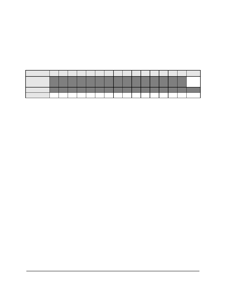
94
56F8346 Technical Data
Preliminary
5.6.22.1 IRQ Pending (PENDING)--Bits 8065
This register combines with the other five to represent the pending IRQs for interrupt vector
numbers 2 through 81.
·
0 = IRQ pending for this vector number
·
1 = No IRQ pending for this vector number
5.6.23
IRQ Pending 5 Register (IRQP5)
Figure 5-25 IRQ Pending Register 5 (IRQP5)
5.6.23.1 Reserved--Bits 9682
This bit field is reserved or not implemented. The bits are read as 1 and cannot be modified by
writing.
5.6.23.2 IRQ Pending (PENDING)--Bit 81
This register combines with the other five to represent the pending IRQs for interrupt vector
numbers 2 through 81.
·
0 = IRQ pending for this vector number
·
1 = No IRQ pending for this vector number
5.6.24
Reserved
--Base + 17
5.6.25
Reserved
--Base + 18
5.6.26
Reserved
--Base + 19
5.6.27
Reserved
--Base + 1A
5.6.28
Reserved
--Base + 1B
5.6.29
Reserved
--Base + 1C
Base + $16
15
14
13
12
11
10
9
8
7
6
5
4
3
2
1
0
Read
1
1
1
1
1
1
1
1
1
1
1
1
1
1
1
PEND-
ING
[81]
Write
RESET
1
1
1
1
1
1
1
1
1
1
1
1
1
1
1
1
F
r
e
e
s
c
a
l
e
S
e
m
i
c
o
n
d
u
c
t
o
r
,
I
Freescale Semiconductor, Inc.
For More Information On This Product,
Go to: www.freescale.com
n
c
.
.
.

Register Descriptions
56F8346 Technical Data
95
Preliminary
5.6.30
ITCN Control Register (ICTL)
Figure 5-26 ITCN Control Register (ICTL)
5.6.30.1 Interrupt (INT)--Bit 15
This read-only bit reflects the state of the interrupt to the 56800E core.
·
0 = No interrupt is being sent to the 56800E core
·
1 = An interrupt is being sent to the 56800E core
5.6.30.2 Interrupt Priority Level (IPIC)--Bits 1413
These read-only bits reflect the state of the new interrupt priority level bits being presented to the
56800E core at the time the last IRQ was taken. This field is only updated when the 56800E core
jumps to a new interrupt service routine.
Note:
Nested interrupts may cause this field to be updated before the original interrupt service
routine can read it.
·
00 = Required nested exception priority levels are 0, 1, 2, or 3
·
01 = Required nested exception priority levels are 1, 2, or 3
·
10 = Required nested exception priority levels are 2 or 3
·
11 = Required nested exception priority level is 3
5.6.30.3 Vector Number - Vector Address Bus (VAB)--Bits 126
This read-only field shows the vector number (VAB[7:1]) used at the time the last IRQ was taken.
This field is only updated when the 56800E core jumps to a new interrupt service routine.
Note:
Nested interrupts may cause this field to be updated before the original interrupt service
routine can read it.
5.6.30.4 Interrupt Disable (INT_DIS)--Bit 5
This bit allows all interrupts to be disabled.
·
0 = Normal operation (default)
·
1 = All interrupts disabled
5.6.30.5 Reserved--Bit 4
This bit field is reserved or not implemented. It is read as 1 and cannot be modified by writing.
5.6.30.6 IRQB State Pin (IRQB STATE)--Bit 3
This read-only bit reflects the state of the external IRQB pin.
Base + $1D
15
14
13
12
11
10
9
8
7
6
5
4
3
2
1
0
Read
INT
IPIC
VAB
INT_DIS
1
IRQB STATE
IRQA STATE
IRQB
EDG
IRQA
EDG
Write
RESET
0
0
0
1
0
0
0
0
0
0
0
1
1
1
0
0
F
r
e
e
s
c
a
l
e
S
e
m
i
c
o
n
d
u
c
t
o
r
,
I
Freescale Semiconductor, Inc.
For More Information On This Product,
Go to: www.freescale.com
n
c
.
.
.

96
56F8346 Technical Data
Preliminary
5.6.30.7 IRQA State Pin (IRQA STATE)--Bit 2
This read-only bit reflects the state of the external IRQA pin.
5.6.30.8 IRQB Edge Pin (IRQB Edg)--Bit 1
This bit controls whether the external IRQB interrupt is edge- or level-sensitive. During Stop and
Wait modes, it is automatically level-sensitive.
·
0 = IRQB interrupt is a low-level sensitive (default)
·
1 = IRQB interrupt is falling-edge sensitive.
5.6.30.9 IRQA Edge Pin (IRQA Edg)--Bit 0
This bit controls whether the external IRQA interrupt is edge- or level-sensitive. During Stop and
Wait modes, it is automatically level-sensitive.
·
0 = IRQA interrupt is a low-level sensitive (default)
·
1 = IRQA interrupt is falling-edge sensitive.
5.7 Resets
5.7.1
Reset Handshake Timing
The ITCN provides the 56800E core with a reset vector address whenever RESET is asserted. The
reset vector will be presented until the second rising clock edge after RESET is released.
5.7.2
ITCN After Reset
After reset, all of the ITCN registers are in their default states. This means all interrupts are
disabled, except the core IRQs with fixed priorities:
·
Illegal Instruction
·
SW Interrupt 3
·
HW Stack Overflow
·
Misaligned Long Word Access
·
SW Interrupt 2
·
SW Interrupt 1
·
SW Interrupt 0
·
SW Interrupt LP
These interrupts are enabled at their fixed priority levels.
F
r
e
e
s
c
a
l
e
S
e
m
i
c
o
n
d
u
c
t
o
r
,
I
Freescale Semiconductor, Inc.
For More Information On This Product,
Go to: www.freescale.com
n
c
.
.
.

Overview
56F8346 Technical Data
97
Preliminary
Part 6 System Integration Module (SIM)
6.1 Overview
The SIM module is a system catchall for the glue logic that ties together the system-on-chip. It
controls distribution of resets and clocks and provides a number of control features. The system
integration module is responsible for the following functions:
·
Reset sequencing
·
Clock generation & distribution
·
Stop/Wait control
·
Pull-up enables for selected peripherals
·
System status registers
·
Registers for software access to the JTAG ID of the chip
·
Enforcing Flash security
These are discussed in more detail in the sections that follow.
6.2 Features
The SIM has the following features:
·
Flash security feature prevents unauthorized access to code/data contained in on-chip Flash
memory
·
Power-saving clock gating for peripheral
·
Three power modes (Run, Wait, Stop) to control power utilization
-- Stop mode shuts down the 56800E core, system clock, peripheral clock, and PLL operation
-- Stop mode entry can optionally disable PLL and Oscillator (low power vs. fast restart); must be
explicitly done
-- Wait mode shuts down the 56800E core and unnecessary system clock operation
-- Run mode supports full part operation
·
Controls to enable/disable the 56800E core WAIT and STOP instructions
·
Calculates base delay for reset extension based upon POR or RESET operations. Reset delay will
be either 3 x 32 clocks (phased release of reset) for reset, except for POR, which is 2
21
clock cycles.
·
Controls reset sequencing after reset
·
Software-initiated reset
·
Four 16-bit registers reset only by a Power-On Reset usable for general-purpose software control
·
System Control Register
·
Registers for software access to the JTAG ID of the chip
F
r
e
e
s
c
a
l
e
S
e
m
i
c
o
n
d
u
c
t
o
r
,
I
Freescale Semiconductor, Inc.
For More Information On This Product,
Go to: www.freescale.com
n
c
.
.
.

98
56F8346 Technical Data
Preliminary
6.3 Operating Modes
Since the SIM is responsible for distributing clocks and resets across the chip, it must understand
the various chip operating modes and take appropriate action. These are:
·
Reset Mode, which has two submodes:
-- POR and RESET operation
The 56800E core and all peripherals are reset. This occurs when the internal POR is asserted or
the RESET pin is asserted.
-- COP reset and software reset operation
The 56800E core and all peripherals are reset. The MA bit within the OMR is not changed. This
allows the software to determine the boot mode (internal or external boot) to be used on the next
reset.
·
Run Mode
This is the primary mode of operation for this device. In this mode, the 56800E controls chip
operation.
·
Debug Mode
The 56800E is controlled via JTAG/EOnCE when in debug mode. All peripherals, except the COP
and PWMs, continue to run. COP is disabled and PWM outputs are optionally switched off to
disable any motor from being driven; see the PWM chapter in the 56F8300 Peripheral User
Manual for details.
·
Wait Mode
In Wait mode, the core clock and memory clocks are disabled. Optionally, the COP can be stopped.
Similarly, it is an option to switch off PWM outputs to disable any motor from being driven. All
other peripherals continue to run.
·
Stop Mode
When in Stop mode, the 56800E core, memory, and most peripheral clocks are shut down.
Optionally, the COP and CAN can be stopped. For lowest power consumption in Stop mode, the
PLL can be shut down. This must be done explicitly before entering Stop mode, since there is no
automatic mechanism for this. The CAN (along with any non-gated interrupt) is capable of waking
the chip up from Stop mode, but is not fully functional in Stop mode.
6.4 Operation Mode Register
Figure 6-1 OMR
See
Section 4.2
for detailed information on how the Operating Mode Register (OMR) MA and MB
bits operate in this device. For additional information on the EX bit, see
Section 4.4
. For all other
bits, see the DSP56800E Reference Manual.
Note:
The OMR is not a Memory Map register; it is directly accessible in code through the acronym
OMR.
Bit
15
14
13
12
11
10
9
8
7
6
5
4
3
2
1
0
NL
CM
XP
SD
R
SA
EX
0
MB
MA
Type
R/W
R/W
R/W
R/W
R/W
R/W
R/W
R/W
R/W
RESET
0
0
0
0
0
0
0
0
0
0
0
0
0
0
0
0
F
r
e
e
s
c
a
l
e
S
e
m
i
c
o
n
d
u
c
t
o
r
,
I
Freescale Semiconductor, Inc.
For More Information On This Product,
Go to: www.freescale.com
n
c
.
.
.

Register Descriptions
56F8346 Technical Data
99
Preliminary
6.5 Register Descriptions
Table 6-1 SIM Registers (SIM_BASE = $00F350)
Address Offset
Address Acronym
Register Name
Section Location
Base + $0
SIM_CONTROL
Control Register
6.5.1
Base + $1
SIM_RSTSTS
Reset Status Register
6.5.2
Base + $2
SIM_SCR0
Software Control Register 0
6.5.3
Base + $3
SIM_SCR1
Software Control Register 1
6.5.3
Base + $4
SIM_SCR2
Software Control Register 2
6.5.3
Base + $5
SIM_SCR3
Software Control Register 3
6.5.3
Base + $6
SIM_MSH_ID
Most Significant Half of JTAG ID
6.5.4
Base + $7
SIM_LSH_ID
Least Significant Half of JTAG ID
6.5.5
Base + $8
SIM_PUDR
Pull-up Disable Register
6.5.6
Reserved
Base + $A
SIM_CLKOSR
CLKO Select Register
6.5.7
Base + $B
SIM_GPS
GPIO Peripheral Select Register
6.5.7
Base + $C
SIM_PCE
Peripheral Clock Enable Register
6.5.8
Base + $D
SIM_ISALH
I/O Short Address Location High Register
6.5.9
Base + $E
SIM_ISALL
I/O Short Address Location Low Register
6.5.10
F
r
e
e
s
c
a
l
e
S
e
m
i
c
o
n
d
u
c
t
o
r
,
I
Freescale Semiconductor, Inc.
For More Information On This Product,
Go to: www.freescale.com
n
c
.
.
.
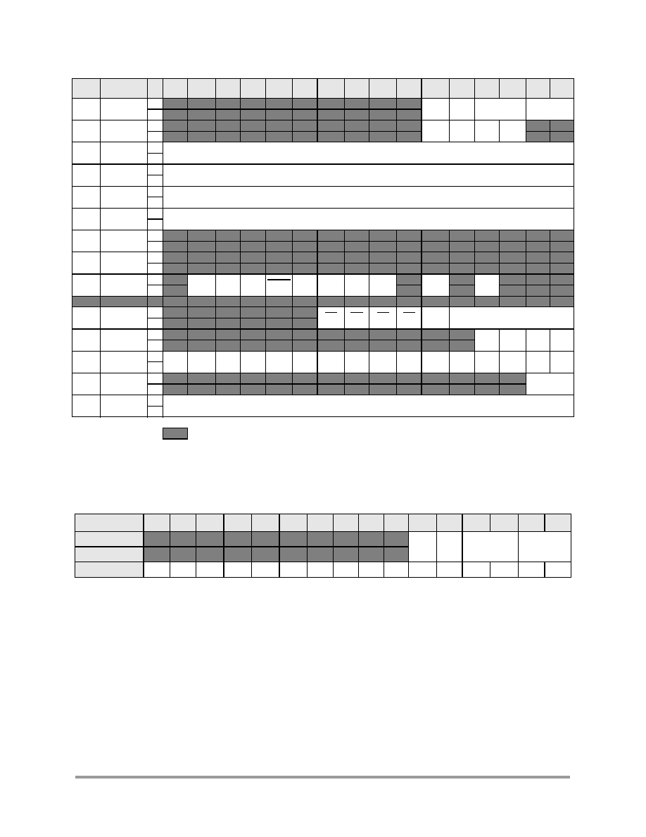
100
56F8346 Technical Data
Preliminary
6.5.1
SIM Control Register (SIM_CONTROL)
Figure 6-3 SIM Control Register (SIM_CONTROL)
6.5.1.1
Reserved--Bits 156
This bit field is reserved or not implemented. It is read as 0 and cannot be modified by writing.
6.5.1.2
OnCE Enable (OnCE EBL)--Bit 5
·
0 = OnCE clock to 56800E core enabled when core TAP is enabled
·
1 = OnCE clock to 56800E core is always enabled
6.5.1.3
Software Reset (SWRST)--Bit 4
This bit is always read as 0. Writing a 1 to this field will cause the part to reset.
Add.
Offset
Register
Name
15
14
13
12
11
10
9
8
7
6
5
4
3
2
1
0
$0
SIM_
CONTROL
R
0
0
0
0
0
0
0
0
0
0
ONCE
EBL
SW
RST
STOP_
DISABLE
WAIT_
DISABLE
W
$1
SIM_
RSTSTS
R
0
0
0
0
0
0
0
0
0
0
SWR
COPR EXTR
POR
0
0
W
$2
SIM_SCR0
R
FIELD
W
$3
SIM_SCR1
R
FIELD
W
$4
SIM_SCR2
R
FIELD
W
$5
SIM_SCR3
R
FIELD
W
$6
SIM_MSH_
ID
R
0
0
0
0
0
0
0
1
1
1
1
1
0
1
0
0
W
$7
SIM_LSH_ID
R
0
1
0
0
0
0
0
0
0
0
0
1
1
1
0
1
W
$8
SIM_PUDR
R
0
PWMA
1
CAN
EMI_
MODE
RESET
IRQ
XBOOT PWMB
PWMA
0
0
CTRL
0
JTAG
0
0
0
W
Reserved
$A
SIM_
CLKOSR
R
0
0
0
0
0
0
A23
A22
A21
A20
CLKDIS
CLKOSEL
W
$B
SIM_GPS
R
0
0
0
0
0
0
0
0
0
0
0
0
C3
C2
C1
C0
W
$C
SIM_PCE
R
EMI
ADCB
ADCA
CAN
DEC1
DEC0
TMRD TMRC
TMRB
TMRA
SCI1
SCI0
SPI1
SPI0
PWM
B
PWM
A
W
$D
SIM_ISALH
R
1
1
1
1
1
1
1
1
1
1
1
1
1
1
ISAL[23:22]
W
$E
SIM_ISALL
R
ISAL[21:6]
W
= Reserved
Figure 6-2 SIM Register Map Summary
Base + $0
15
14
13
12
11
10
9
8
7
6
5
4
3
2
1
0
Read
0
0
0
0
0
0
0
0
0
0
ONCE
EBL
SW
RST
STOP_
DISABLE
WAIT_
DISABLE
Write
RESET
0
0
0
0
0
0
0
0
0
0
0
0
0
0
0
0
F
r
e
e
s
c
a
l
e
S
e
m
i
c
o
n
d
u
c
t
o
r
,
I
Freescale Semiconductor, Inc.
For More Information On This Product,
Go to: www.freescale.com
n
c
.
.
.

Register Descriptions
56F8346 Technical Data
101
Preliminary
6.5.1.4
Stop Disable (STOP_DISABLE)--Bits 32
·
00 - STOP mode will be entered when the 56800E core executes a STOP instruction
·
01 - The 56800E STOP instruction will not cause entry into Stop mode; STOP_DISABLE can be
reprogrammed in the future
·
10 - The 56800E STOP instruction will not cause entry into Stop mode; STOP_DISABLE can then
only be changed by resetting the device
·
11 - Same operation as 10
6.5.1.5
Wait Disable (WAIT_DISABLE)--Bits 10
·
00 - WAIT mode will be entered when the 56800E core executes a WAIT instruction
·
01 - The 56800E WAIT instruction will not cause entry into Wait mode; WAIT_DISABLE can be
reprogrammed in the future
·
10 - The 56800E WAIT instruction will not cause entry into Wait mode; WAIT_DISABLE can then
only be changed by resetting the device
·
11 - Same operation as 10
6.5.2
SIM Reset Status Register (SIM_RSTSTS)
Bits in this register are set upon any system reset and are initialized only by a Power-On Reset
(POR). A reset (other than POR) will only set bits in the register; bits are not cleared. Only software
should clear this register.
Figure 6-4 SIM Reset Status Register (SIM_RSTSTS)
6.5.2.1
Reserved--Bits 156
This bit field is reserved or not implemented. It is read as 0 and cannot be modified by writing.
6.5.2.2
Software Reset (SWR)--Bit 5
When 1, this bit indicates that the previous reset occurred as a result of a software reset (write to
SW RST bit in the SIM_CONTROL register). This bit will be cleared by any hardware reset or by
software. Writing a 0 to this bit position will set the bit, while writing a 1 to the bit will clear it.
6.5.2.3
COP Reset (COPR)--Bit 4
When 1, the COPR bit indicates the Computer Operating Properly (COP) timer-generated reset has
occurred. This bit will be cleared by a Power-On Reset or by software. Writing a 0 to this bit
position will set the bit, while writing a 1 to the bit will clear it.
Base + $1
15
14
13
12
11
10
9
8
7
6
5
4
3
2
1
0
Read
0
0
O
0
0
0
0
0
0
0
SWR
COPR
EXTR
POR
0
0
Write
RESET
0
0
0
0
0
0
0
0
0
0
0
0
F
r
e
e
s
c
a
l
e
S
e
m
i
c
o
n
d
u
c
t
o
r
,
I
Freescale Semiconductor, Inc.
For More Information On This Product,
Go to: www.freescale.com
n
c
.
.
.
102
56F8346 Technical Data
Preliminary
6.5.2.4
External Reset (EXTR)--Bit 3
If 1, the EXTR bit indicates an external system reset has occurred. This bit will be cleared by a
Power-On Reset or by software. Writing a 0 to this bit position will set the bit, while writing a 1 to
the bit position will clear it. Basically, when the EXTR bit is 1, the previous system reset was
caused by the external RESET pin being asserted low.
6.5.2.5
Power-On Reset (POR)--Bit 2
When 1, the POR bit indicates a Power-On Reset occurred some time in the past. This bit can be
cleared only by software or by another type of reset. Writing a 0 to this bit will set the bit, while
writing a 1 to the bit position will clear the bit. In summary, if the bit is 1, the previous system reset
was due to a Power-On Reset.
6.5.2.6
Reserved--Bits 10
This bit field is reserved or not implemented. It is read as 0 and cannot be modified by writing.
6.5.3
SIM Software Control Registers (SIM_SCR0, SIM_SCR1,
SIM_SCR2, and SIM_SCR3)
Only SIM_SCR0 is shown below. SIM_SCR1, SIM_SCR2, and SIM_SCR3 are identical in
functionality.
Figure 6-5 SIM Software Control Register 0 (SIM_SCR0)
6.5.3.1
Software Control Data 1 (FIELD)--Bits 150
This register is reset only by the Power-On Reset (POR). It has no part-specific functionality and
is intended for use by a software developer to contain data that will be unaffected by the other reset
sources (RESET pin, software reset, and COP reset).
6.5.4
Most Significant Half of JTAG ID (SIM_MSH_ID)
This read-only register displays the most significant half of the JTAG ID for the chip. This register
reads $01F4.
Figure 6-6 Most Significant Half of JTAG ID (SIM_MSH_ID)
Base + $2
15
14
13
12
11
10
9
8
7
6
5
4
3
2
1
0
Read
FIELD
Write
POR
0
0
0
0
0
0
0
0
0
0
0
0
0
0
0
0
Base + $6
15
14
13
12
11
10
9
8
7
6
5
4
3
2
1
0
Read
0
0
0
0
0
0
0
1
1
1
1
1
0
1
0
0
Write
RESET
0
0
0
0
0
0
0
1
1
1
1
1
0
1
0
0
F
r
e
e
s
c
a
l
e
S
e
m
i
c
o
n
d
u
c
t
o
r
,
I
Freescale Semiconductor, Inc.
For More Information On This Product,
Go to: www.freescale.com
n
c
.
.
.
Register Descriptions
56F8346 Technical Data
103
Preliminary
6.5.5
Least Significant Half of JTAG ID (SIM_LSH_ID)
This read-only register displays the least significant half of the JTAG ID for the chip. This register
reads $401D.
Figure 6-7 Least Significant Half of JTAG ID (SIM_LSH_ID)
6.5.6
SIM Pull-up Disable Register (SIM_PUDR)
Most of the pins on the chip have on-chip pull-up resistors. Pins which can operate as GPIO can
have these resistors disabled via the GPIO function. Non-GPIO pins can have their pull-ups
disabled by setting the appropriate bit in this register. Disabling pull-ups is done on a
peripheral-by-peripheral basis (for pins not muxed with GPIO). Each bit in the register (see
Figure 6-8
) corresponds to a functional group of pins. See
Table 2-2
to identify which pins can
deactivate the internal pull-up resistor.
Figure 6-8 SIM Pull-up Disable Register (SIM_PUDR)
6.5.6.1
Reserved--Bit 15
This bit field is reserved or not implemented. It is read as 0 and cannot be modified by writing.
6.5.6.2
PWMA1--Bit 14
This bit controls the pull-up resistors on the FAULTA3 pin.
6.5.6.3
CAN--Bit 13
This bit controls the pull-up resistors on the CAN_RX pin.
6.5.6.4
EMI_MODE--Bit 12
This bit controls the pull-up resistors on the EMI_MODE pin.
6.5.6.5
RESET--Bit 11
This bit controls the pull-up resistors on the RESET pin.
6.5.6.6
IRQ--Bit 10
This bit controls the pull-up resistors on the IRQA and IRQB pins.
Base + $7
15
14
13
12
11
10
9
8
7
6
5
4
3
2
1
0
Read
0
1
0
0
0
0
0
0
0
0
0
1
1
1
0
1
Write
RESET
0
1
0
0
0
0
0
0
0
0
0
1
1
1
0
1
Base + $8
15
14
13
12
11
10
9
8
7
6
5
4
3
2
1
0
Read
0
PWMA1
CAN
EMI_
MODE
RESET
IRQ
XBOOT
PWMB
PWMA0
0
CTRL
0
JTAG
0
0
0
Write
RESET
0
0
0
0
0
0
0
0
0
0
0
0
0
0
0
0
F
r
e
e
s
c
a
l
e
S
e
m
i
c
o
n
d
u
c
t
o
r
,
I
Freescale Semiconductor, Inc.
For More Information On This Product,
Go to: www.freescale.com
n
c
.
.
.

104
56F8346 Technical Data
Preliminary
6.5.6.7
XBOOT--Bit 9
This bit controls the pull-up resistors on the EXTBOOT pin.
6.5.6.8
PWMB--Bit 8
This bit controls the pull-up resistors on the FAULTB0, FAULTB1, FAULTB2, and FAULTB3
pins.
6.5.6.9
PWMA0--Bit 7
This bit controls the pull-up resistors on the FAULTA0, FAULTA1, and FAULTA2 pins.
6.5.6.10 Reserved--Bit 6
This bit field is reserved or not implemented. It is read as 0 and cannot be modified by writing.
6.5.6.11 CTRL--Bit 5
This bit controls the pull-up resistors on the WR and RD pins.
6.5.6.12 Reserved--Bit 4
This bit field is reserved or not implemented. It is read as 0 and cannot be modified by writing.
6.5.6.13 JTAG--Bit 3
This bit controls the pull-up resistors on the TRST, TMS and TDI pins.
6.5.6.14 Reserved--Bits 2 - 0
This bit field is reserved or not implemented. It is read as 0 and cannot be modified by writing.
6.5.7
CLKO Select Register (SIM_CLKOSR)
The CLKO select register can be used to multiplex out any one of the clocks generated inside the
clock generation and SIM modules. The default value is SYS_CLK. All other clocks primarily
muxed out are for test purposes only, and are subject to significant unspecified latencies at high
frequencies.
The upper four bits of the GPIO B register can function as GPIOA23 through A20, or as additional
clock output signals. GPIO has priority and is enabled/disabled via the GPIOB_PER. If GPIO
B[7:4] are programmed to operate as peripheral outputs, then the choice between A23 through A20
and additional clock outputs is done here in the CLKOSR. The default state is for the peripheral
function of GPIO B[7:4] to be programmed as A23 through A20. This can be changed by altering
A23 through A20, as shown in
Figure 6-9
.
Figure 6-9 CLKO Select Register (SIM_CLKOSR)
Base + $A
15
14
13
12
11
10
9
8
7
6
5
4
3
2
1
0
Read
0
0
0
0
0
0
A23
A22
A21
A20
CLK
DIS
CLKOSEL
Write
RESET
0
0
0
0
0
0
0
0
0
0
1
0
0
0
0
0
F
r
e
e
s
c
a
l
e
S
e
m
i
c
o
n
d
u
c
t
o
r
,
I
Freescale Semiconductor, Inc.
For More Information On This Product,
Go to: www.freescale.com
n
c
.
.
.

Register Descriptions
56F8346 Technical Data
105
Preliminary
6.5.7.1
Reserved--Bits 1510
This bit field is reserved or not implemented. It is read as 0 and cannot be modified by writing.
6.5.7.2
Alternate GPIO_B Peripheral Function Select for A23 (A23)--Bit 9
·
0 = Peripheral output function of GPIO B[7] is defined to be A[23]
·
1 = Peripheral output function of GPIO B[7] is defined to be the oscillator clock (MSTR_OSC, see
Figure 3-4
)
6.5.7.3
Alternate GPIO_B Peripheral Function Select for A22 (A22)--Bit 8
·
0 = Peripheral output function of GPIO B[6] is defined to be A[22]
·
1 = Peripheral output function of GPIO B[6] is defined to be SYS_CLK2
6.5.7.4
Alternate GPIO_B Peripheral Function Select for A21 (A21)--Bit 7
·
0 = Peripheral output function of GPIO B[5] is defined to be A[21]
·
1 = Peripheral output function of GPIO B[5] is defined to be SYS_CLK
6.5.7.5
Alternate GPIO_B Peripheral Function Select for A20 (A20)--Bit 6
·
0 = Peripheral output function of GPIO B[4] is defined to be A[20]
·
1 = Peripheral output function of GPIO B[4] is defined to be the prescaler clock (FREF, see
Figure 3-4
)
6.5.7.6
Clockout Disable (CLKDIS)--Bit 5
·
0 = CLKOUT output is enabled and will output the signal indicated by CLKOSEL
·
1 = CLKOUT is tri-stated
6.5.7.7
CLockout Select (CLKOSEL)--Bits 40
Selects clock to be muxed out on the CLKO pin.
·
00000 = SYS_CLK (from OCCS - DEFAULT)
·
00001 = Reserved for factory test--56800E clock
·
00010 = Reserved for factory test--XRAM clock
·
00011 = Reserved for factory test--PFLASH odd clock
·
00100 = Reserved for factory test--PFLASH even clock
·
00101 = Reserved for factory test--BFLASH clock
·
00110 = Reserved for factory test--DFLASH clock
·
00111 = Oscillator output
·
01000 = F
out
(from OCCS)
·
01001 = Reserved for factory test--IPB clock
·
01010 = Reserved for factory test--Feedback (from OCCS, this is path to PLL)
·
01011 = Reserved for factory test--Prescaler clock (from OCCS)
·
01100 = Reserved for factory test--Postscaler clock (from OCCS)
·
01101 = Reserved for factory test--SYS_CLK2 (from OCCS)
·
01110 = Reserved for factory test--SYS_CLK_DIV2
·
01111 = Reserved for factory test--SYS_CLK_D
·
10000 = ADCA clock
·
10001 = ADCB clock
F
r
e
e
s
c
a
l
e
S
e
m
i
c
o
n
d
u
c
t
o
r
,
I
Freescale Semiconductor, Inc.
For More Information On This Product,
Go to: www.freescale.com
n
c
.
.
.

106
56F8346 Technical Data
Preliminary
6.5.8
GPIO Peripheral Select Register (SIM_GPS)
The GPIO Peripheral Select register can be used to multiplex out any one of the three alternate
peripherals for GPIOC. The default peripheral is Quad Decoder 1 and Quad Timer B; these
peripherals work together.
The four I/O pins associated with GPIO C can function as GPIO, Quad Decoder 1/Quad Timer B,
or as SPI 1 signals. GPIO is not the default and is enabled/disabled via the GPIOC_PER, as shown
in
Figure 6-10
and
Table 6-2
. When GPIO C[3:0] are programmed to operate as peripheral I/O,
then the choice between decoder/timer and SPI inputs/outputs is made in the SIM_GPS register and
in conjunction with the Quad Timer Status and Control Registers (SCR). The default state is for
the peripheral function of GPIO C[3:0] to be programmed as decoder functions. This can be
changed by altering the appropriate controls in the indicated registers.
Figure 6-10 Overall Control of Pads Using SIM_GPS Control
GPIOC_PER Register
GPIO Controlled
I/O
Pad Control
SIM_
GPS Register
Quad Timer Controlled
SPI Controlled
0
1
0
1
F
r
e
e
s
c
a
l
e
S
e
m
i
c
o
n
d
u
c
t
o
r
,
I
Freescale Semiconductor, Inc.
For More Information On This Product,
Go to: www.freescale.com
n
c
.
.
.
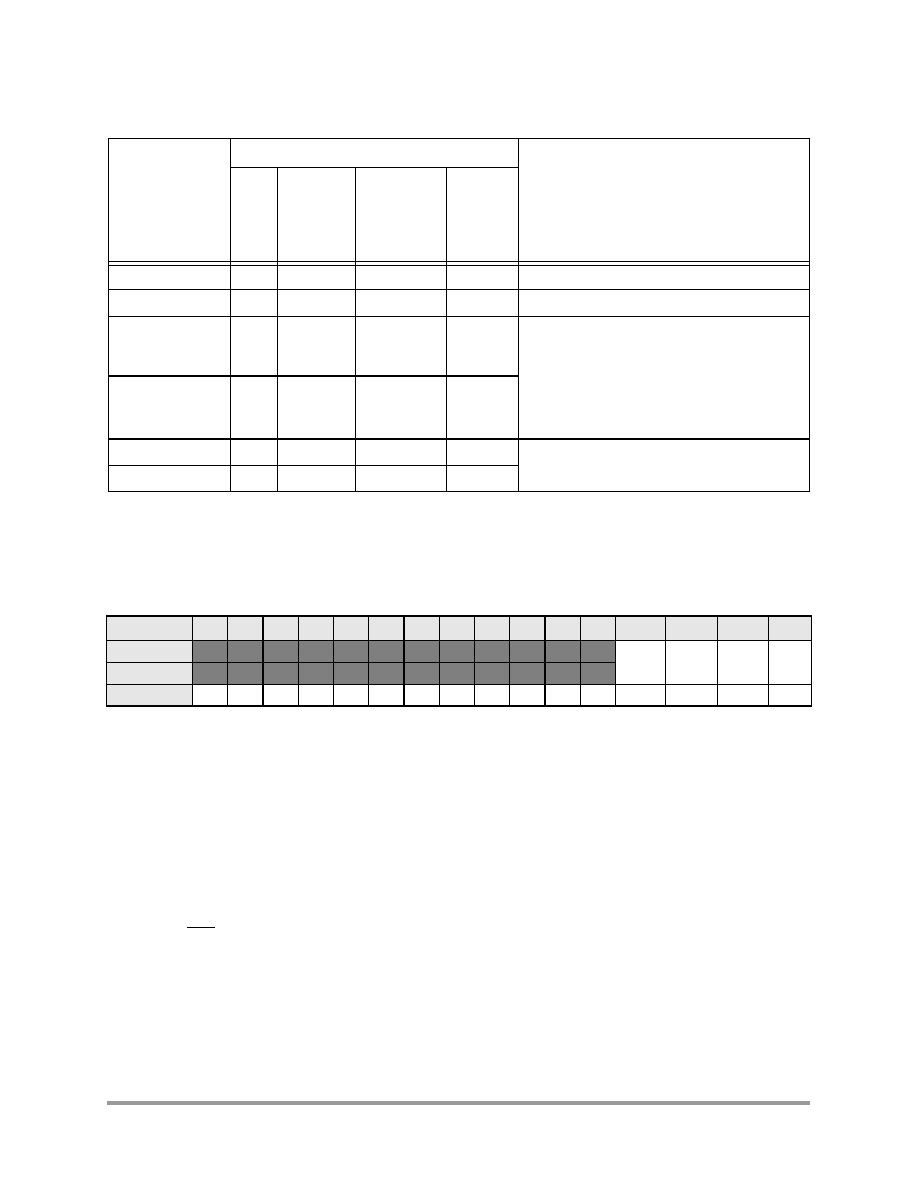
Register Descriptions
56F8346 Technical Data
107
Preliminary
Figure 6-11 GPIO Peripheral Select Register (SIM_GPS)
6.5.8.1
Reserved--Bits 154
This bit field is reserved or not implemented. It is read as 0 and cannot be modified by writing.
6.5.8.2
GPIO C3 (C3)--Bit 3
This bit selects the alternate function for GPIOC3.
·
0 = HOME1/TB3 (default - see "Switch Matrix Mode" bits of the Quad Decoder DECCR register
in the 56F8300 Peripheral User Manual)
·
1 = SS1
6.5.8.3
GPIO C2 (C2)--Bit 2
This bit selects the alternate function for GPIOC2.
·
0 = INDEX1/TB2 (default)
·
1 = MISO1
Table 6-2 Control of Pads Using SIM_GPS Control
1
1.
This applies to the four pins that serve as Quad Decoder / Quad Timer / SPI / GPIOC functions. A separate set of control
bits is used for each pin.
Pin Function
Control Registers
Comments
GPIOC_PER
GPIOC_
DTR
SI
M
_
G
PS
Q
u
ad
T
im
er
SCR Re
g
i
s
t
e
r
OEN
b
i
ts
GPIO Input
0
0
--
--
GPIO Output
0
1
--
--
Quad Timer Input /
Quad Decoder
Input
2
2.
Reset configuration
1
--
0
0
See the "Switch Matrix for Inputs to the Timer"
table in the 56F8300 Peripheral User Manual
for the definition of the timer inputs based on
the Quad Decoder Mode configuration.
Quad Timer
Output / Quad
Decoder Input
3
3.
Quad Decoder pins are always inputs and function in conjunction with the Quad Timer pins.
1
--
0
1
SPI input
1
--
1
--
See SPI controls for determining the direction
of each of the SPI pins.
SPI output
1
--
1
--
Base + $B
15
14
13
12
11
10
9
8
7
6
5
4
3
2
1
0
Read
0
0
0
0
0
0
0
0
0
0
0
0
C3
C2
C1
C0
Write
RESET
0
0
0
0
0
0
0
0
0
0
0
0
0
0
0
0
F
r
e
e
s
c
a
l
e
S
e
m
i
c
o
n
d
u
c
t
o
r
,
I
Freescale Semiconductor, Inc.
For More Information On This Product,
Go to: www.freescale.com
n
c
.
.
.

108
56F8346 Technical Data
Preliminary
6.5.8.4
GPIO C1 (C1)--Bit 1
This bit selects the alternate function for GPIOC1.
·
0 = PHASEB1/TB1 (default)
·
1 = MOSI1
6.5.8.5
GPIO C0 (C0)--Bit 0
This bit selects the alternate function for GPIOC0.
·
0 = PHASEA1/TB0 (default)
·
1 = SCLK1
6.5.9
Peripheral Clock Enable Register (SIM_PCE)
The Peripheral Clock Enable register is used to enable or disable clocks to the peripherals as a
power savings feature. The clocks can be individually controlled for each peripheral on the chip.
Figure 6-12 Peripheral Clock Enable Register (SIM_PCE)
6.5.9.1
External Memory Interface Enable (EMI)--Bit 15
Each bit controls clocks to the indicated peripheral.
·
1 = Clocks are enabled
·
0 = The clock is not provided to the peripheral (the peripheral is disabled)
6.5.9.2
Analog-to-Digital Converter B Enable (ADCB)--Bit 14
Each bit controls clocks to the indicated peripheral.
·
1 = Clocks are enabled
·
0 = The clock is not provided to the peripheral (the peripheral is disabled)
6.5.9.3
Analog-to-Digital Converter A Enable (ADCA)--Bit 13
Each bit controls clocks to the indicated peripheral.
·
1 = Clocks are enabled
·
0 = The clock is not provided to the peripheral (the peripheral is disabled)
6.5.9.4
FlexCAN Enable (CAN)--Bit 12
Each bit controls clocks to the indicated peripheral.
·
1 = Clocks are enabled
·
0 = The clock is not provided to the peripheral (the peripheral is disabled)
Base + $C
15
14
13
12
11
10
9
8
7
6
5
4
3
2
1
0
Read
EMI
ADCB ADCA
CAN
DEC1
DEC0
TMRD TMRC
TMRB
TMRA
SCI 1
SCI 0
SPI 1
SPI 0
PWMB
PWMA
Write
RESET
1
1
1
1
1
1
1
1
1
1
1
1
1
1
1
1
F
r
e
e
s
c
a
l
e
S
e
m
i
c
o
n
d
u
c
t
o
r
,
I
Freescale Semiconductor, Inc.
For More Information On This Product,
Go to: www.freescale.com
n
c
.
.
.

Register Descriptions
56F8346 Technical Data
109
Preliminary
6.5.9.5
Decoder 1 Enable (DEC1)--Bit 11
Each bit controls clocks to the indicated peripheral.
·
1 = Clocks are enabled
·
0 = The clock is not provided to the peripheral (the peripheral is disabled)
6.5.9.6
Decoder 0 Enable (DEC0)--Bit 10
Each bit controls clocks to the indicated peripheral.
·
1 = Clocks are enabled
·
0 = The clock is not provided to the peripheral (the peripheral is disabled)
6.5.9.7
Quad Timer D Enable (TMRD)--Bit 9
Each bit controls clocks to the indicated peripheral.
·
1 = Clocks are enabled
·
0 = The clock is not provided to the peripheral (the peripheral is disabled)
6.5.9.8
Quad Timer C Enable (TMRC)--Bit 8
Each bit controls clocks to the indicated peripheral.
·
1 = Clocks are enabled
·
0 = The clock is not provided to the peripheral (the peripheral is disabled)
6.5.9.9
Quad Timer B Enable (TMRB)--Bit 7
Each bit controls clocks to the indicated peripheral.
·
1 = Clocks are enabled
·
0 = The clock is not provided to the peripheral (the peripheral is disabled)
6.5.9.10 Quad Timer A Enable (TMRA)--Bit 6
Each bit controls clocks to the indicated peripheral.
·
1 = Clocks are enabled
·
0 = The clock is not provided to the peripheral (the peripheral is disabled)
6.5.9.11 Serial Communications Interface 1 Enable (SCI1)--Bit 5
Each bit controls clocks to the indicated peripheral.
·
1 = Clocks are enabled
·
0 = The clock is not provided to the peripheral (the peripheral is disabled)
6.5.9.12 Serial Communications Interface 0 Enable (SCI0)--Bit 4
Each bit controls clocks to the indicated peripheral.
·
1 = Clocks are enabled
·
0 = The clock is not provided to the peripheral (the peripheral is disabled)
F
r
e
e
s
c
a
l
e
S
e
m
i
c
o
n
d
u
c
t
o
r
,
I
Freescale Semiconductor, Inc.
For More Information On This Product,
Go to: www.freescale.com
n
c
.
.
.

110
56F8346 Technical Data
Preliminary
6.5.9.13 Serial Peripheral Interface 1 Enable (SPI1)--Bit 3
Each bit controls clocks to the indicated peripheral.
·
1 = Clocks are enabled
·
0 = The clock is not provided to the peripheral (the peripheral is disabled)
6.5.9.14 Serial Peripheral Interface 0 Enable (SPI0)--Bit 2
Each bit controls clocks to the indicated peripheral.
·
1 = Clocks are enabled
·
0 = The clock is not provided to the peripheral (the peripheral is disabled)
6.5.9.15 Pulse Width Modulator B Enable (PWMB)--1
Each bit controls clocks to the indicated peripheral.
·
1 = Clocks are enabled
·
0 = The clock is not provided to the peripheral (the peripheral is disabled)
6.5.9.16 Pulse Width Modulator A Enable (PWMA)--0
Each bit controls clocks to the indicated peripheral.
·
1 = Clocks are enabled
·
0 = The clock is not provided to the peripheral (the peripheral is disabled)
6.5.10
I/O Short Address Location Register (SIM_ISALH and
SIM_ISALL)
The I/O Short Address Location registers are used to specify the memory referenced via the I/O
short address mode. The I/O short address mode allows the instruction to specify the lower six bits
of address; the upper address bits are not directly controllable. This register set allows limited
control of the full address, as shown in
Figure 6-13
.
Note:
If this register is set to something other than the top of memory (EOnCE register space) and
the EX bit in the OMR is set to 1, the JTAG port cannot access the on-chip EOnCE registers,
and debug functions will be affected.
F
r
e
e
s
c
a
l
e
S
e
m
i
c
o
n
d
u
c
t
o
r
,
I
Freescale Semiconductor, Inc.
For More Information On This Product,
Go to: www.freescale.com
n
c
.
.
.
Register Descriptions
56F8346 Technical Data
111
Preliminary
Figure 6-13 I/O Short Address Determination
With this register set, an interrupt driver can set the SIM_ISALL register pair to point to its
peripheral registers and then use the I/O Short addressing mode to reference them. The ISR should
restore this register to its previous contents prior to returning from interrupt.
Note:
The default value of this register set points to the EOnCE registers.
Note:
The pipeline delay between setting this register set and using short I/O addressing with the
new value is three cycles.
Figure 6-14 I/O Short Address Location High Register (SIM_ISALH)
6.5.10.1 Input/Output Short Address Low (ISAL[23:22])--Bit 10
This field represents the upper two address bits of the "hard coded" I/O short address.
Figure 6-15 I/O Short Address Location Low Register (SIM_ISALL)
6.5.10.2 Input/Output Short Address Low (ISAL[21:6])--Bit 150
This field represents the lower 16 address bits of the "hard coded" I/O short address.
Base + $D
15
14
13
12
11
10
9
8
7
6
5
4
3
2
1
0
Read
1
1
1
1
1
1
1
1
1
1
1
1
1
1
ISAL[23:22]
Write
RESET
1
1
1
1
1
1
1
1
1
1
1
1
1
1
1
1
Base + $E
15
14
13
12
11
10
9
8
7
6
5
4
3
2
1
0
Read
ISAL[21:6]
Write
RESET
1
1
1
1
1
1
1
1
1
1
1
1
1
1
1
1
Instruction Portion
"
Hard Coded" Address Portion
6 Bits from I/O Short Address Mode Instruction
16 Bits from SIM_ISALL Register
2 bits from SIM_ISALH Register
Full 24-Bit for Short I/O Address
F
r
e
e
s
c
a
l
e
S
e
m
i
c
o
n
d
u
c
t
o
r
,
I
Freescale Semiconductor, Inc.
For More Information On This Product,
Go to: www.freescale.com
n
c
.
.
.

112
56F8346 Technical Data
Preliminary
6.6 Clock Generation Overview
The SIM uses an internal master clock from the OCCS (CLKGEN) module to produce the
peripheral and system (core and memory) clocks. The maximum master clock frequency is
120MHz. Peripheral and system clocks are generated at half the master clock frequency and
therefore at a maximum 60MHz. The SIM provides power modes (Stop, Wait) and clock enables
(SIM_PCE register, CLK_DIS, ONCE_EBL) to control which clocks are in operation. The OCCS,
power modes, and clock enables provide a flexible means to manage power consumption.
Power utilization can be minimized in several ways. In the OCCS, crystal oscillator, and PLL may
be shut down when not in use. When the PLL is in use, its prescaler and postscaler can be used to
limit PLL and master clock frequency. Power modes permit system and/or peripheral clocks to be
disabled when unused. Clock enables provide the means to disable individual clocks. Some
peripherals provide further controls to disable unused subfunctions. Refer to the
Part 3, On-Chip
Clock Synthesis (OCCS)
and the 56F8300 Peripheral User Manual for further details.
6.7 Power-Down Modes Overview
The 56F8346 operates in one of three power-down modes, as shown in
Table 6-3
.
All peripherals, except the COP/watchdog timer, run off the IPBus clock frequency, which is the
same as the main processor frequency in this architecture. The maximum frequency of operation
is SYS_CLK = 60MHz.
Table 6-3 Clock Operation in Power-Down Modes
Mode
Core Clocks
Peripheral Clocks
Description
Run
Active
Active
Device is fully functional
Wait
Core and memory
clocks disabled
Active
Peripherals are active and can product interrupts if they
have not been masked off.
Interrupts will cause the core to come out of its
suspended state and resume normal operation.
Typically used for power-conscious applications.
Stop
System clocks continue to be generated in
the SIM, but most are gated prior to
reaching memory, core and peripherals.
The only possible recoveries from Stop mode are:
1. CAN traffic (1st message will be lost)
2. Non-clocked interrupts
3. COP reset
4. External reset
5. Power-on reset
F
r
e
e
s
c
a
l
e
S
e
m
i
c
o
n
d
u
c
t
o
r
,
I
Freescale Semiconductor, Inc.
For More Information On This Product,
Go to: www.freescale.com
n
c
.
.
.
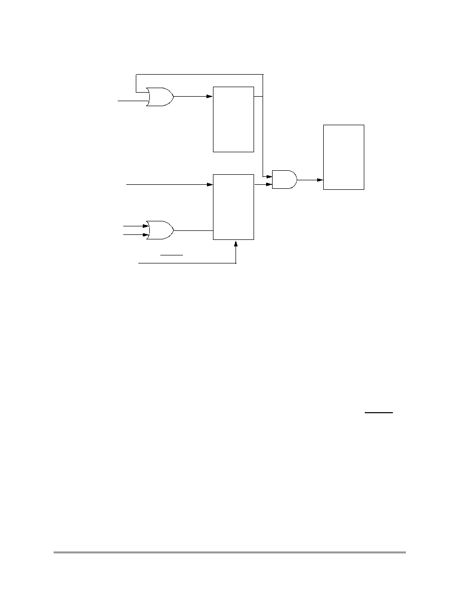
Stop and Wait Mode Disable Function
56F8346 Technical Data
113
Preliminary
6.8 Stop and Wait Mode Disable Function
Figure 6-16 Internal Stop Disable Circuit
The 56800E core contains both STOP and WAIT instructions. Both put the CPU to sleep. For
lowest power consumption in Stop mode, the PLL can be shut down. This must be done explicitly
before entering Stop mode, since there is no automatic mechanism for this. When the PLL is shut
down, the 56800E system clock must be set equal to the prescaler output.
Some applications require the 56800E STOP and WAIT instructions be disabled. To disable those
instructions, write to the SIM control register (SIM_CONTROL), described in
Section 6.5.1
. This
procedure can be on either a permanent or temporary basis. Permanently assigned applications last
only until their next reset.
6.9 Resets
The SIM supports four sources of reset. The two asynchronous sources are the external RESET pin
and the Power-On Reset (POR). The two synchronous sources are the software reset, which is
generated within the SIM itself by writing to the SIM_CONTROL register, and the COP reset.
Reset begins with the assertion of any of the reset sources. Release of reset to various blocks is
sequenced to permit proper operation of the device. A POR reset is first extended for 2
21
clock
cycles to permit stabilization of the clock source, followed by a 32 clock window in which SIM
clocking is initiated. It is then followed by a 32 clock window in which peripherals are released to
implement Flash security, and, finally, followed by a 32 clock window in which the core is
initialized. After completion of the described reset sequence, application code will begin
execution.
Resets may be asserted asynchronously, but they are always released internally on a rising edge of
the system clock.
D-FLOP
D
Q
C
D-FLOP
D
Q
C
R
56800E
STOP_DIS
Permanent
Disable
Reprogrammable Disable
Clock
Select
RESET
Note: Wait disable circuit is similar
F
r
e
e
s
c
a
l
e
S
e
m
i
c
o
n
d
u
c
t
o
r
,
I
Freescale Semiconductor, Inc.
For More Information On This Product,
Go to: www.freescale.com
n
c
.
.
.

114
56F8346 Technical Data
Preliminary
Part 7 Security Features
The 56F8346 offers security features intended to prevent unauthorized users from reading the
contents of the Flash Memory (FM) array. The 56F8346's Flash security consists of several
hardware interlocks that block the means by which an unauthorized user could gain access to the
Flash array.
However, part of the security must lie with the user's code. An extreme example would be user's
code that dumps the contents of the internal program, as this code would defeat the purpose of
security. At the same time, the user may also wish to put a "backdoor" in his program. As an
example, the user downloads a security key through the SCI, allowing access to a programming
routine that updates parameters stored in another section of the Flash.
7.1 Operation with Security Enabled
Once the user has programmed the Flash with his application code, the 56F8346 can be secured by
programming the security bytes located in the FM configuration field, which occupies a portion of
the FM array. These non-volatile bytes will keep the part secured through reset and through
power-down of the device. Only two bytes within this field are used to enable or disable security.
Refer to the Flash Memory section in the 56F8300 Peripheral User Manual for the state of the
security bytes and the resulting state of security. When Flash security mode is enabled in
accordance with the method described in the Flash Memory module specification, the 56F8346
will disable external P-space accesses restricting code execution to internal memory, disable
EXTBOOT=1 mode, and disable the core EOnCE debug capabilities. Normal program execution
is otherwise unaffected.
7.2 Flash Access Blocking Mechanisms
The 56F8346 has several operating functional and test modes. Effective Flash security must
address operating mode selection and anticipate modes in which the on-chip Flash can be
compromised and read without explicit user permission. Methods to block these are outlined in the
next subsections.
7.2.1
Forced Operating Mode Selection
At boot time, the SIM determines in which functional modes the 56F8346 will operate. These are:
·
Internal Boot Mode
·
External Boot Mode
·
Secure Mode
When Flash security is enabled as described in the Flash Memory module specification, the
56F8346 will boot in internal boot mode, disable all access to external P-space, and start executing
code from the Boot Flash at address 0x02_0000.
This security affords protection only to applications in which the 56F8346 operates in internal
Flash security mode. Therefore, the security feature cannot be used unless all executing code
resides on-chip.
When security is enabled, any attempt to override the default internal operating mode by asserting
the EXTBOOT pin in conjunction with reset will be ignored.
F
r
e
e
s
c
a
l
e
S
e
m
i
c
o
n
d
u
c
t
o
r
,
I
Freescale Semiconductor, Inc.
For More Information On This Product,
Go to: www.freescale.com
n
c
.
.
.

Flash Access Blocking Mechanisms
56F8346 Technical Data
115
Preliminary
7.2.2
Disabling EOnCE Access
On-chip Flash can be read by issuing commands across the EOnCE port, which is the debug
interface for the 56800E core. The TRST, TCLK, TMS, TDO, and TDI pins comprise a JTAG
interface onto which the EOnCE port functionality is mapped. When the 56F8346 boots, the
chip-level JTAG TAP (Test Access Port) is active and provides the chip's boundary scan capability
and access to the ID register.
Proper implementation of Flash security requires that no access to the EOnCE port is provided
when security is enabled. The 56800E core has an input which disables reading of internal memory
via the JTAG/EOnCE. The FM sets this input at reset to a value determined by the contents of the
FM security bytes.
7.2.3
Flash LOCKOUT_RECOVERY
If a user inadvertently enables security on the 56F8346, a lockout recovery mechanism is provided
which allows the complete erasure of the internal Flash contents, including the configuration field,
and thus disables security (the protection register is cleared). This does not compromise security,
as the entire contents of the user's secured code stored in Flash are erased before security is
disabled on the 56F8346 on the next reset or power-up sequence. To start the lockout recovery
sequence, the JTAG public instruction (LOCKOUT_RECOVERY) must first be shifted into the
chip-level TAP controller's instruction register.
The LOCKOUT_RECOVERY instruction has an associated 7-bit Data Register (DR) that is used
to control the clock divider circuit within the FM module. This divider, FM_CLKDIV[6:0], is used
to control the period of the clock used for timed events in the FM erase algorithm. This register
must be set with appropriate values before the lockout sequence can begin. Refer to the JTAG
section of the 56F8300 Peripheral User Manual for more details on setting this register value.
The value of the JTAG FM_CLKDIV[6:0] will replace the value of the FM register FMCLKD that
divides down the system clock for timed events, as illustrated in
Figure 7-1
. FM_CLKDIV[6] will
map to the PRDIV8 bit, and FM_CLKDIV[5:0] will map to the DIV[5:0] bits. The combination of
PRDIV8 and DIV must divide the FM input clock down to a frequency of 150kHz-200kHz. The
"Writing the FMCLKD Register" section in the Flash Memory chapter of the 56F8300
Peripheral User Manual gives specific equations for calculating the correct values.
F
r
e
e
s
c
a
l
e
S
e
m
i
c
o
n
d
u
c
t
o
r
,
I
Freescale Semiconductor, Inc.
For More Information On This Product,
Go to: www.freescale.com
n
c
.
.
.
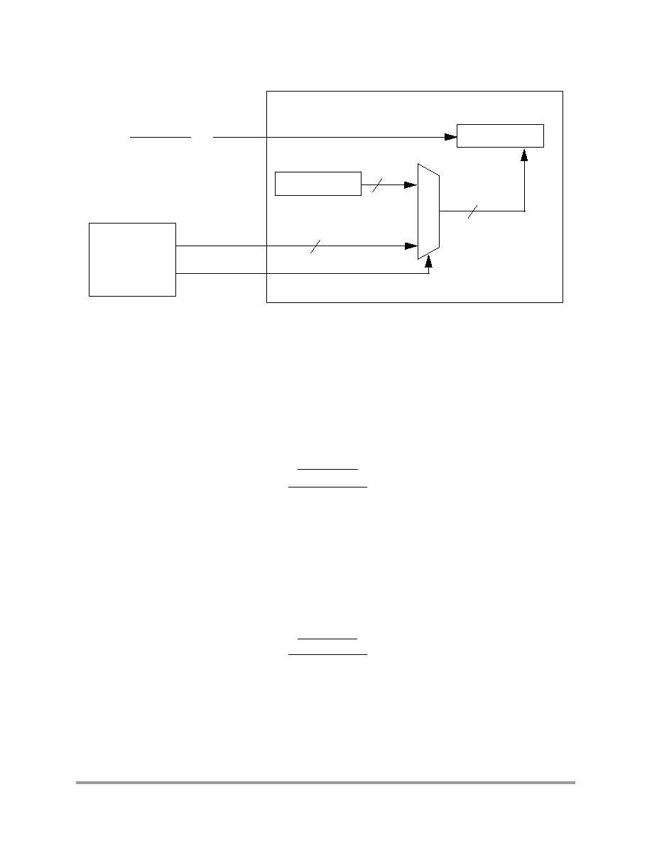
116
56F8346 Technical Data
Preliminary
Figure 7-1 JTAG to FM Connection for LOCKOUT_RECOVERY
Two examples of FM_CLKDIV calculations follow.
EXAMPLE 1: If the system clock is the 8MHz crystal frequency because the PLL has not been
set up, the input clock will be below 12.8MHz, so PRDIV8 = FM_CLKDIV[6] = 0. Using the
following equation yields a DIV value of 19 for a clock of 200kHz, and a DIV value of 20 for a
clock of 190kHz. This translates into an FM_CLKDIV[6:0] value of $13 or $14, respectively.
EXAMPLE 2: In this example, the system clock has been set up with a value of 32MHz, making
the FM input clock 16MHz. Because that is greater than 12.8MHz, PRDIV8 = FM_CLKDIV[6] =
1. Using the following equation yields a DIV value of 9 for a clock of 200kHz, and a DIV value of
10 for a clock of 181kHz. This translates to an FM_CLKDIV[6:0] value of $49 or $4A,
respectively.
SYS_CLK
JTAG
FMCLKD
DIVIDER
7
7
7
2
FM_CLKDIV
FM_ERASE
Flash Memory
clock
input
SYS_CLK
(2)
)
(
<
<
(DIV + 1)
150[kHz]
200[kHz]
)
(
<
<
(DIV + 1)
150[kHz]
200[kHz]
SYS_CLK
(2)
F
r
e
e
s
c
a
l
e
S
e
m
i
c
o
n
d
u
c
t
o
r
,
I
Freescale Semiconductor, Inc.
For More Information On This Product,
Go to: www.freescale.com
n
c
.
.
.

Flash Access Blocking Mechanisms
56F8346 Technical Data
117
Preliminary
Once the LOCKOUT_RECOVERY instruction has been shifted into the instruction register, the
clock divider value must be shifted into the corresponding 7-bit data register. After the data register
has been updated, the user must transition the TAP controller into the RUN-TEST/IDLE state for
the lockout sequence to commence. The controller must remain in this state until the erase
sequence has completed. For details, see the JTAG Section in the 56F8300 Peripheral User
Manual.
Note:
Once the lockout recovery sequence has completed, the user must reset both the JTAG TAP
controller (by asserting TRST) and the 56F8346 (by asserting external chip reset) to return to
normal unsecured operation.
7.2.4
Product Analysis
The recommended method of unsecuring a programmed 56F8346 for product analysis of field
failures is via the backdoor key access. The customer would need to supply Motorola with the
backdoor key and the protocol to access the backdoor routine in the Flash. Additionally, the
KEYEN bit that allows backdoor key access must be set.
An alternative method for performing analysis on a secured hybrid controller would be to
mass-erase and reprogram the Flash with the original code, but modify the security bytes.
To insure that a customer does not inadvertently lock himself out of the 56F8346 during
programming, it is recommended that he program the backdoor access key first, his application
code second, and the security bytes within the FM configuration field last.
F
r
e
e
s
c
a
l
e
S
e
m
i
c
o
n
d
u
c
t
o
r
,
I
Freescale Semiconductor, Inc.
For More Information On This Product,
Go to: www.freescale.com
n
c
.
.
.

118
56F8346 Technical Data
Preliminary
Part 8 General Purpose Input/Output (GPIO)
8.1 Introduction
This section is intended to supplement the GPIO information found in the 56F8300 Peripheral
User Manual and contains only chip-specific information. This information supercedes the
generic information in the 56F8300 Peripheral User Manual.
8.2 Configuration
There are six GPIO ports defined on the 56F8346. The width of each port and the associated
peripheral function is shown in
Table 8-1
. The specific mapping of GPIO port pins is shown in
Table 8-2
.
Table 8-1 GPIO Ports Configuration
GPIO
Port
Port
Width
Available
Pins in
56F8346
Peripheral Function
Reset Function
A
14
14
14 pins - EMI Address pins
EMI Address
B
8
1
1 pin - EMI Address pin
7 pins - EMI Address pins - Not available in this package
EMI Address
N/A
C
11
11
4 pins -DEC1 / TMRB / SPI1
4 pins -DEC0 / TMRA
3 pins -PWMA current sense
DEC1 / TMRB
DEC0 / TMRA
PWMA current sense
D
13
9
2 pins - EMI CSn
4 pins - EMI CSn - Not available in this package
2 pins - SCI1
2 pins - EMI CSn
3 pins -PWMB current sense
EMI Chip Selects
N/A
SCI1
EMI Chip Selects
PWMB current sense
E
14
11
2 pins - SCI0
2 pins - EMI Address pins
4 pins - SPI0
1 pin - TMRC
1 pin - TMRC
2 pins - TMRD
2 pins - TMRD
SCI0
EMI Address
SPI0
TMRC
N/A
TMRD
N/A
F
16
16
16 pins - EMI Data
EMI Data
F
r
e
e
s
c
a
l
e
S
e
m
i
c
o
n
d
u
c
t
o
r
,
I
Freescale Semiconductor, Inc.
For More Information On This Product,
Go to: www.freescale.com
n
c
.
.
.

Configuration
56F8346 Technical Data
119
Preliminary
Table 8-2 GPIO External Signals Map
Pins in shaded rows are not available in 56F8346
GPIO Port
GPIO Bit
Reset
Function
Functional Signal
Package Pin
GPIOA
0
Peripheral
A8
19
1
Peripheral
A9
20
2
Peripheral
A10
21
3
Peripheral
A11
22
4
Peripheral
A12
23
5
Peripheral
A13
24
6
Peripheral
A14
25
7
Peripheral
A15
26
8
Peripheral
A0
138
9
Peripheral
A1
10
10
Peripheral
A2
11
11
Peripheral
A3
12
12
Peripheral
A4
13
13
Peripheral
A5
14
GPIOB
0
GPIO
A16
33
1
N/A
2
N/A
3
N/A
4
N/A
5
N/A
6
N/A
7
N/A
F
r
e
e
s
c
a
l
e
S
e
m
i
c
o
n
d
u
c
t
o
r
,
I
Freescale Semiconductor, Inc.
For More Information On This Product,
Go to: www.freescale.com
n
c
.
.
.
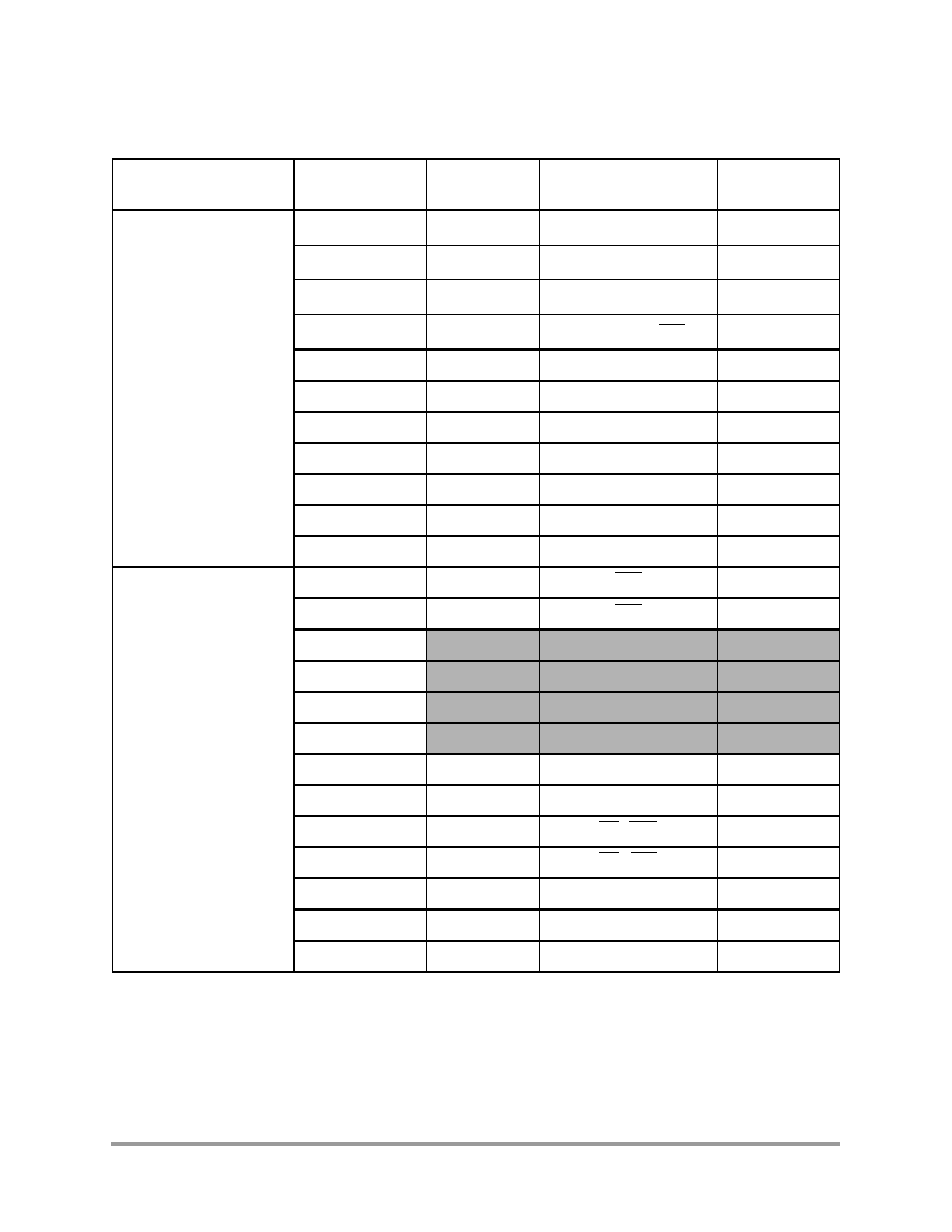
120
56F8346 Technical Data
Preliminary
GPIOC
0
Peripheral
PhaseA1 / TB0 / SCLK1
1
6
1
Peripheral
PhaseB1 / TB1 / MOSI1
1
7
2
Peripheral
Index1 / TB2 / MISO1
1
8
3
Peripheral
Home1 / TB3 / SS1
1
9
4
Peripheral
PHASEA0 / TA0
139
5
Peripheral
PHASEB0 / TA1
140
6
Peripheral
Index0 / TA2
141
7
Peripheral
Home0 / TA3
142
8
Peripheral
ISA0
113
9
Peripheral
ISA1
114
10
Peripheral
ISA2
115
GPIOD
0
GPIO
CS2
48
1
GPIO
CS3
49
2
N/A
3
N/A
4
N/A
5
N/A
6
Peripheral
TXD1
42
7
Peripheral
RXD1
43
8
Peripheral
PS / CS0
46
9
Peripheral
DS / CS1
47
10
Peripheral
ISB0
50
11
Peripheral
ISB1
52
12
Peripheral
ISB2
53
Table 8-2 GPIO External Signals Map (Continued)
Pins in shaded rows are not available in 56F8346
GPIO Port
GPIO Bit
Reset
Function
Functional Signal
Package Pin
F
r
e
e
s
c
a
l
e
S
e
m
i
c
o
n
d
u
c
t
o
r
,
I
Freescale Semiconductor, Inc.
For More Information On This Product,
Go to: www.freescale.com
n
c
.
.
.
Configuration
56F8346 Technical Data
121
Preliminary
GPIOE
0
Peripheral
TXD0
4
1
Peripheral
RXD0
5
2
Peripheral
A6
17
3
Peripheral
A7
18
4
Peripheral
SCLK0
130
5
Peripheral
MOSI0
132
6
Peripheral
MISO0
131
7
Peripheral
SS0
129
8
Peripheral
TC0
118
9
N/A
10
Peripheral
TD0
116
11
Peripheral
TD1
117
12
N/A
13
N/A
Table 8-2 GPIO External Signals Map (Continued)
Pins in shaded rows are not available in 56F8346
GPIO Port
GPIO Bit
Reset
Function
Functional Signal
Package Pin
F
r
e
e
s
c
a
l
e
S
e
m
i
c
o
n
d
u
c
t
o
r
,
I
Freescale Semiconductor, Inc.
For More Information On This Product,
Go to: www.freescale.com
n
c
.
.
.

122
56F8346 Technical Data
Preliminary
8.3 Memory Maps
The width of the GPIO port defines how many bits are implemented in each of the GPIO registers.
Based on this and the default function of each of the GPIO pins, the reset values of the GPIOx_PUR
and GPIOx_PER registers change from port to port. Tables
4-29
through
4-34
define the actual
reset values of these registers for the 56F8346.
Part 9 Joint Test Action Group (JTAG)
9.1 56F8346 Information
Please contact your Motorola marketing representative for device/package-specific BSDL
information.
GPIOF
0
Peripheral
D7
28
1
Peripheral
D8
29
2
Peripheral
D9
30
3
Peripheral
D10
32
4
Peripheral
D11
133
5
Peripheral
D12
134
6
Peripheral
D13
135
7
Peripheral
D14
136
8
Peripheral
D15
137
9
Peripheral
D0
59
10
Peripheral
D1
60
11
Peripheral
D2
72
12
Peripheral
D3
75
13
Peripheral
D4
76
14
Peripheral
D5
77
15
Peripheral
D6
78
1.
See
Section 6.5.8
to determine how to select peripherals from this set; DEC1 is the selected peripheral at reset .
Table 8-2 GPIO External Signals Map (Continued)
Pins in shaded rows are not available in 56F8346
GPIO Port
GPIO Bit
Reset
Function
Functional Signal
Package Pin
F
r
e
e
s
c
a
l
e
S
e
m
i
c
o
n
d
u
c
t
o
r
,
I
Freescale Semiconductor, Inc.
For More Information On This Product,
Go to: www.freescale.com
n
c
.
.
.

General Characteristics
56F8346 Technical Data
123
Preliminary
Part 10 Specifications
10.1 General Characteristics
The 56F8346 is fabricated in high-density CMOS with 5V-tolerant TTL-compatible digital inputs.
The term "5V-tolerant" refers to the capability of an I/O pin, built on a 3.3V-compatible process
technology, to withstand a voltage up to 5.5V without damaging the device. Many systems have a
mixture of devices designed for 3.3V and 5V power supplies. In such systems, a bus may carry both
3.3V- and 5V-compatible I/O voltage levels (a standard 3.3V I/O is designed to receive a
maximum voltage of 3.3V
±
10% during normal operation without causing damage). This
5V-tolerant capability therefore offers the power savings of 3.3V I/O levels combined with the
ability to receive 5V levels without damage.
Absolute maximum ratings in
Table 10-1
are stress ratings only, and functional operation at the
maximum is not guaranteed. Stress beyond these ratings may affect device reliability or cause
permanent damage to the device.
Note:
All specifications meet both Automotive and Industrial requirements unless individual
specifications are listed.
CAUTION
This device contains protective circuitry to guard
against damage due to high static voltage or electrical
fields. However, normal precautions are advised to
avoid application of any voltages higher than
maximum-rated voltages to this high-impedance circuit.
Reliability of operation is enhanced if unused inputs are
tied to an appropriate voltage level.
F
r
e
e
s
c
a
l
e
S
e
m
i
c
o
n
d
u
c
t
o
r
,
I
Freescale Semiconductor, Inc.
For More Information On This Product,
Go to: www.freescale.com
n
c
.
.
.

124
56F8346 Technical Data
Preliminary
Note: The overall life of this device may be reduced if subjected to extended use over 110C
junction. For additional information, please contact your sales representative.
Table 10-1 Absolute Maximum Ratings
(V
SS
= V
SSA_ADC
=
0)
Characteristic
Symbol
Notes
Min
Max
Unit
Supply voltage
V
DD_IO
- 0.3
4.0
V
ADC Supply Voltage
V
DDA_ADC,
V
REFH
V
REFH
must be
less than or equal
to
V
DDA_ADC
- 0.3
4.0
V
Oscillator / PLL Supply Voltage
V
DDA_OSC_PLL
- 0.3
4.0
V
Internal Logic Core Supply Voltage
V
DDA_CORE
OCR_DIS is High
- 0.3
3.0
V
Input Voltage (digital)
V
IN
Pin Groups
1, 2, 5, 6, 9, 10, 14
-0.3
6.0
V
Input Voltage (analog)
V
INA
Pin Groups
11, 12, 13
-0.3
4.0
V
Output Voltage
V
OUT
Pin Groups
1, 2, 3, 4, 5, 6, 7, 8
-0.3
4.0
V
Output Voltage (open drain)
V
OD
Pin Groups
4, 14
-0.3
6.0
V
Ambient Temperature (Automotive)
T
A
-40
125
°C
Ambient Temperature (Industrial)
T
A
-40
105
°C
Junction Temperature (Automotive)
T
J
-40
150
°C
Junction Temperature (Industrial)
T
J
-40
125
°C
Storage Temperature (Automotive)
T
STG
-55
150
°C
Storage Temperature (Industrial)
T
STG
-55
150
°C
Pin Group 1: TXD0-1, RXD0-1, SS0, MISO0, MOSI0
Pin Group 2: PHASEA0-1, PHASEB0-1, INDEX0-1,
HOME0-1, ISB0-2, RSTO, ISA0-2, TC0,
SCLK0
Pin Group 3: RSTO, TDO
Pin Group 4: CAN_TX
Pin Group 5: A0-5, D0-15, GPIOD0-1, PS, DS
Pin Group 6: A6-15, GPIOB0, TD0-1
Pin Group 7: CLKO, WR, RD
Pin Group 8: PWMA0-5, PWMB0-5
Pin Group 9: IRQA, IRQB, RESET, EXTBOOT, TRST,
TMS,
TDI,
CAN_RX,
EMI_MODE,
FAULTA0-3, FAULTB0-3
Pin Group 10: TCK
Pin Group 11: XTAL, EXTAL
Pin Group 12: ANA0-7, ANB0-7
Pin Group 13: OCR_DIS, CLKMODE
F
r
e
e
s
c
a
l
e
S
e
m
i
c
o
n
d
u
c
t
o
r
,
I
Freescale Semiconductor, Inc.
For More Information On This Product,
Go to: www.freescale.com
n
c
.
.
.

General Characteristics
56F8346 Technical Data
125
Preliminary
Notes:
1.
Theta-JA determined on 2s2p test boards is frequently lower than would be observed in an application.
Determined on 2s2p thermal test board.
2.
Junction to ambient thermal resistance, Theta-JA (R
JA
) was simulated to be equivalent to the JEDEC
specification JESD51-2 in a horizontal configuration in natural convection. Theta-JA was also simulated on a
thermal test board with two internal planes (2s2p, where "s" is the number of signal layers and "p" is the number
of planes) per JESD51-6 and JESD51-7. The correct name for Theta-JA for forced convection or with the
non-single layer boards is Theta-JMA.
3.
Junction to case thermal resistance, Theta-JC (R
JC
), was simulated to be equivalent to the measured values
using the cold plate technique with the cold plate temperature used as the "case" temperature. The basic cold
plate measurement technique is described by MIL-STD 883D, Method 1012.1. This is the correct thermal
metric to use to calculate thermal performance when the package is being used with a heat sink.
4.
Thermal Characterization Parameter, Psi-JT (
JT
), is the "resistance" from junction to reference point
thermocouple on top center of case as defined in JESD51-2.
JT
is a useful value to use to estimate junction
temperature in steady-state customer environments.
5.
Junction temperature is a function of on-chip power dissipation, package thermal resistance, mounting site
(board) temperature, ambient temperature, air flow, power dissipation of other components on the board, and
board thermal resistance.
6.
See
Section 12.1
for more details on thermal design considerations.
Table 10-2 Electrostatic Discharge Protection
Characteristic
Min
Typ
Max
Unit
ESD for Human Body Model (HBM)
2000
--
--
V
ESD for Machine Model (MM)
200
--
--
V
ESD for Charge Device Model (CDM)
500
--
--
V
Table 10-3 Thermal Characteristics
6
Characteristic
Comments
Symbol
Value
Unit
Notes
144-pin LQFP
Junction to ambient
Natural convection
R
JA
47.1
°C/W
2
Junction to ambient (@1m/sec)
R
JMA
43.8
°C/W
2
Junction to ambient
Natural convection
Four layer board
(2s2p)
R
JMA
(2s2p)
40.8
°C/W
1,2
Junction to ambient (@1m/sec)
Four layer board
(2s2p)
R
JMA
39.2
°C/W
1,2
Junction to case
R
JC
11.8
°C/W
3
Junction to center of case
JT
1
°C/W
4, 5
I/O pin power dissipation
P
I/O
User-determined
W
Power dissipation
P
D
P
D
= (I
DD
x V
DD
+ P
I/O
)
W
Maximum allowed P
D
P
DMAX
(TJ - TA) /
JA
°C
F
r
e
e
s
c
a
l
e
S
e
m
i
c
o
n
d
u
c
t
o
r
,
I
Freescale Semiconductor, Inc.
For More Information On This Product,
Go to: www.freescale.com
n
c
.
.
.

126
56F8346 Technical Data
Preliminary
Note: Total chip source or sink current cannot exceed 200mA
See Pin Groups in
Table 10-1
Table 10-4 Recommended Operating Conditions
(V
REFLO
= 0V, V
SS
= V
SSA_ADC
= 0V
,
V
DDA
= V
DDA_ADC
= V
DDA_OSC_PLL
)
Characteristic
Symbol
Notes
Min
Typ
Max
Unit
Supply voltage
V
DD_IO
3
3.3
3.6
V
ADC Supply Voltage
V
DDA_ADC,
V
REFH
V
REFH
must be
less than or equal
to V
DDA_ADC
3
3.3
3.6
V
Oscillator / PLL Supply Voltage
V
DDA_OSC
_PLL
3
3.3
3.6
V
Internal Logic Core Supply
Voltage
V
DD_CORE
OCR_DIS is High
2.25
2.5
2.75
V
Device Clock Frequency
FSYSCLK
0
--
60
MHz
Input High Voltage (digital)
V
IN
Pin Groups
1, 2, 5, 6, 9, 10
2
--
5.5
V
Input High Voltage (analog)
V
IHA
Pin Group 13
2
--
V
DDA
+0.3
V
Input High Voltage (XTAL/EXTAL,
XTAL is not driven by an external
clock)
V
IHC
Pin Group 11
V
DDA
-0.8
--
V
DDA
+0.3
V
Input high voltage (XTAL/EXTAL,
XTAL is driven by an external clock)
V
IHC
Pin Group 11
2
--
V
DDA
+0.3
V
Input Low Voltage
V
IL
Pin Groups
1, 2, 5, 6, 9, 10,
11, 13
-0.3
--
0.8
V
Output High Source Current
V
OH
= 2.4V (V
OH
min.)
I
OH
Pin Groups 1, 2, 3
--
--
-4
mA
Pin Groups 5, 6, 7
--
--
-8
Pin Group 8
--
--
-12
Output Low Sink Current
V
OL
= 0.4V (V
OL
max)
I
OL
Pin Groups
1, 2, 3, 4
--
--
4
mA
Pin Groups 5, 6, 7
--
--
8
Pin Group 8
--
--
12
Ambient Operating Temperature
(Automotive)
T
A
-40
--
125 -
(R
JA
X P
D
)
°C
Ambient Operating Temperature
(Industrial)
T
A
-40
--
105 -
(R
JA
X P
D
)
°C
Flash Endurance (Automotive)
(Program Erase Cycles)
N
F
T
A
= -40°C
to
125°C
10,000
--
--
Cycles
Flash Endurance (Industrial)
(Program Erase Cycles)
N
F
T
A
= -40°C
to
105°C
10,000
--
--
Cycles
Flash Data Retention
T
R
T
J
<= 70°C
avg
15
--
--
Years
F
r
e
e
s
c
a
l
e
S
e
m
i
c
o
n
d
u
c
t
o
r
,
I
Freescale Semiconductor, Inc.
For More Information On This Product,
Go to: www.freescale.com
n
c
.
.
.

DC Electrical Characteristics
56F8346 Technical Data
127
Preliminary
10.2 DC Electrical Characteristics
See Pin Groups in
Table 10-1
Table 10-5 DC Electrical Characteristics
Over Recommended Operating Conditions, V
DDA
= V
DDA_ADC,_
V
DDA_OSC_PLL
Characteristic
Symbol
Notes
Min
Typ
Max
Unit
Test
Conditions
Output High Voltage
V
OH
2.4
--
--
V
I
OH
=I
OHmax
Output Low Voltage
V
OL
--
--
0.4
V
I
OL
=I
OLmax
Digital Input Current High
pull-up enabled or disabled
I
IH
Pin Groups
1, 2, 5, 6, 9
--
0
+/- 2.5
µ
A
V
IN
= 3.0V to 5.5V
Digital Input Current High
with pull-down
I
IH
Pin Group 10
40
80
160
µ
A
V
IN
= 3.0V to 5.5V
Analog Input Current High
I
IHA
Pin Group 13
--
0
+/- 2.5
µ
A
V
IN
= V
DDA
ADC Input Current High
I
IHADC
Pin Group 12
--
0
+/- 3.5
µ
A
V
IN
= V
DDA
Digital Input Current Low
pull-up enabled
I
IL
Pin Groups
1, 2, 5, 6, 9
-200
-100
-50
µ
A
V
IN
= 0V
Digital Input Current Low
pull-up disabled
I
IL
Pin Groups
1, 2, 5, 6, 9
--
0
+/- 2.5
µ
A
V
IN
= 0V
Digital Input Current Low
with pull-down
I
IL
Pin Group 10
--
0
+/- 2.5
µ
A
V
IN
= 0V
Analog Input Current Low
I
ILA
Pin Group 13
--
0
+/- 2.5
µ
A
V
IN
= 0V
ADC Input Current Low
I
ILADC
Pin Group 12
--
0
+/- 3.5
µ
A
V
IN
= 0V
EXTAL Input Current Low
clock input
I
EXTAL
--
0
+/- 2.5
µ
A
V
IN
= V
DDA
or 0V
XTAL Input Current Low
clock input
I
XTAL
CLKMODE =
High
--
0
+/- 2.5
µ
A
V
IN
= V
DDA
or 0V
CLKMODE =
Low
--
--
200
µ
A
V
IN
= V
DDA
or 0V
Output Current
High Impedance State
I
OZ
Pin Groups
1, 2, 3, 4, 5,
6, 7, 8
--
0
+/- 2.5
µ
A
V
OUT
= 3.0V to
5.5V or 0V
Schmitt Trigger Input
Hysteresis
V
HYS
Pin Groups
2, 6, 9,10
--
0.3
--
V
--
Input Capacitance
(EXTAL/XTAL)
C
INC
--
4.5
--
pF
--
Output Capacitance
(EXTAL/XTAL)
C
OUTC
--
5.5
--
pF
--
Input Capacitance
C
IN
--
6
--
pF
--
Output Capacitance
C
OUT
--
6
--
pF
--
F
r
e
e
s
c
a
l
e
S
e
m
i
c
o
n
d
u
c
t
o
r
,
I
Freescale Semiconductor, Inc.
For More Information On This Product,
Go to: www.freescale.com
n
c
.
.
.

128
56F8346 Technical Data
Preliminary
Table 10-6 Power on Reset Low Voltage Parameters
Characteristic
Symbol
Min
Typ
Max
Units
POR Trip Point
POR
1.75
1.8
1.9
V
LVI, 2.5 volt Supply, trip point
1
1.
When V
DD
drops below V
EI2.5
, an interrupt is generated.
V
EI2.5
--
2.14
--
V
LVI, 3.3 volt supply, trip point
2
2.
When V
DD
drops below V
EI3.3
, an interrupt is generated.
V
EI3.3
--
2.7
--
V
Bias Current
I
bias
--
110
130
µ
A
Table 10-7 Current Consumption per Power Supply Pin (Typical)
On-Chip Regulator Enabled (OCR_DIS = Low)
Mode
I
DD_IO
1
1.
No Output Switching
I
DD_ADC
I
DD_OSC_PLL
Test Conditions
RUN1_MAC
155mA
50mA
2.5mA
· 60MHz Device Clock
· All peripheral clocks are enabled
· All peripherals running
· Continuous MAC instructions with fetches from
Data RAM
· ADC powered on and clocked
Wait3
91mA
65
µ
A
2.5mA
· 60MHz Device Clock
· All peripheral clocks are enabled
· ADC powered off
Stop1
5.8mA
0
µ
A
155
µ
A
· 8MHz Device Clock
· All peripheral clocks are off
· ADC powered off
· PLL powered off
Stop2
5.1mA
0
µ
A
145
µ
A
· External Clock is off
· All peripheral clocks are off
· ADC powered off
· PLL powered off
F
r
e
e
s
c
a
l
e
S
e
m
i
c
o
n
d
u
c
t
o
r
,
I
Freescale Semiconductor, Inc.
For More Information On This Product,
Go to: www.freescale.com
n
c
.
.
.

DC Electrical Characteristics
56F8346 Technical Data
129
Preliminary
Table 10-8 Current Consumption per Power Supply Pin (Typical)
On-Chip Regulator Disabled (OCR_DIS = High)
Mode
I
DD_Core
I
DD_IO
1
1.
No Output Switching
I
DD_ADC
I
DD_OSC_PLL
Test Conditions
RUN1_MAC
150mA
13
µ
A
50mA
2.5mA
· 60MHz Device Clock
· All peripheral clocks are enabled
· All peripherals running
· Continuous MAC instructions with
fetches from Data RAM
· ADC powered on and clocked
Wait3
86mA
13
µ
A
65
µ
A
2.5mA
· 60MHz Device Clock
· All peripheral clocks are enabled
· All peripherals running
· ADC powered off
Stop1
800
µ
A
13
µ
A
0
µ
A
155
µ
A
· 8MHz Device Clock
· All peripheral clocks are off
· ADC powered off
· PLL powered off
Stop2
100
µ
A
13
µ
A
0
µ
A
145
µ
A
· External Clock is off
· All peripheral clocks are off
· ADC powered off
· PLL powered off
Table 10-9. Regulator Parameters
Characteristic
Symbol
Min
Typical
Max
Unit
Unloaded Output Voltage
(0mA Load)
V
RNL
2.25
--
2.75
V
Loaded Output Voltage
(250mA load)
V
RL
2.25
--
2.75
V
Line Regulation @ 250mA load
(V
DD
33 ranges from 3.0V to 3.6V)
V
R
2.25
--
2.75
V
Short Circuit Current
(output shorted to ground)
Iss
--
--
700
mA
Bias Current
I
bias
--
5.8
7
mA
Power-down Current
I
pd
--
0
2
µ
A
Short-Circuit Tolerance
(output shorted to ground)
T
RSC
--
--
30
minutes
F
r
e
e
s
c
a
l
e
S
e
m
i
c
o
n
d
u
c
t
o
r
,
I
Freescale Semiconductor, Inc.
For More Information On This Product,
Go to: www.freescale.com
n
c
.
.
.
130
56F8346 Technical Data
Preliminary
10.3 Temperature Sense
10.4 AC Electrical Characteristics
Tests are conducted using the input levels specified in
Table 10-5
. Unless otherwise specified,
propagation delays are measured from the 50% to the 50% point, and rise and fall times are
measured between the 10% and 90% points, as shown in
Figure 10-1
.
Figure 10-1 Input Signal Measurement References
Table 10-10. PLL Parameters
Characteristics
Symbol
Min
Typical
Max
Unit
PLL Start-up time
T
PS
0.3
0.5
10
ms
Resonator Start-up time
T
RS
0.1
0.18
1
ms
Min-Max Period Variation
T
PV
120
--
200
ps
Peak-to-Peak Jitter
T
PJ
--
--
175
ps
Bias Current
I
BIAS
--
1.5
2
mA
Quiescent Current, power-down mode
I
PD
--
100
150
µ
A
Table 10-11 Temperature Sense Parametrics
Characteristics
Symbol
Min
Typical
Max
Unit
K-factor
1
1.
This is the inverse of the parameter "m" found in the Functional Description of the Temperature Sensor chapter of the
56F8300 Peripheral User Manual.
K
7
7.2
--
mV/°C
Supply Voltage
V
DDA
3.0
3.3
3.6
V
Supply Current - OFF
I
DD-OFF
--
--
10
µ
A
Supply Current - ON
I
DD-ON
--
--
250
µ
A
Accuracy
T
ACC
-2
--
+2
°C
Resolution
R
ES
--
--
1
°C / bit
2
2.
Assuming a 10-bit range from 0V to 3.6V.
V
IH
V
IL
Fall Time
Input Signal
Note: The midpoint is V
IL
+ (V
IH
V
IL
)/2.
Midpoint1
Low
High
90%
50%
10%
Rise Time
F
r
e
e
s
c
a
l
e
S
e
m
i
c
o
n
d
u
c
t
o
r
,
I
Freescale Semiconductor, Inc.
For More Information On This Product,
Go to: www.freescale.com
n
c
.
.
.
Flash Memory Characteristics
56F8346 Technical Data
131
Preliminary
Figure 10-2
shows the definitions of the following signal states:
·
Active state, when a bus or signal is driven, and enters a low impedance state
·
Tri-stated, when a bus or signal is placed in a high impedance state
·
Data Valid state, when a signal level has reached V
OL
or V
OH
·
Data Invalid state, when a signal level is in transition between V
OL
and V
OH
Figure 10-2 Signal States
10.5 Flash Memory Characteristics
Table 10-12 Flash Timing Parameters
Characteristic
Symbol
Min
Typ
Max
Unit
Program time
1
1.
There is additional overhead which is part of the programming sequence. See the 56F8300 Peripheral User Manual for
details. Program time is per 16-bit word in Flash memory. Two words at a time can be programmed within the Program Flash
module, as it contains two interleaved memories.
T
prog
20
--
--
µ
s
Erase time
2
2.
Specifies page erase time. There are 512 bytes per page in the Data and Boot Flash memories. The Program Flash mod-
ule uses two interleaved Flash memories, increasing the effective page size to 1024 bytes.
T
erase
20
--
--
ms
Mass erase time
T
me
100
--
--
ms
Data Invalid State
Data1
Data2 Valid
Data
Tri-stated
Data3 Valid
Data2
Data3
Data1 Valid
Data Active
Data Active
F
r
e
e
s
c
a
l
e
S
e
m
i
c
o
n
d
u
c
t
o
r
,
I
Freescale Semiconductor, Inc.
For More Information On This Product,
Go to: www.freescale.com
n
c
.
.
.
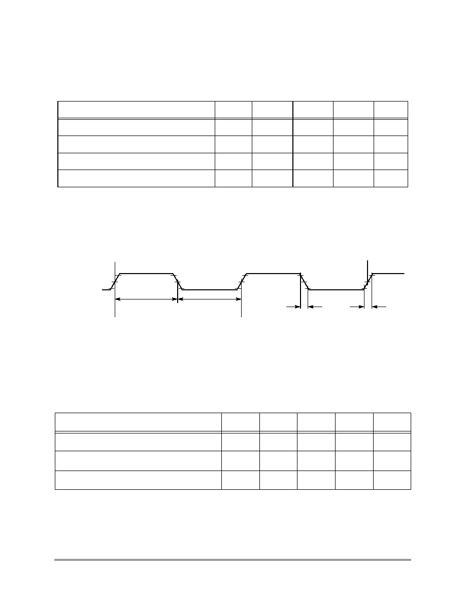
132
56F8346 Technical Data
Preliminary
10.6 External Clock Operation Timing
Figure 10-3 External Clock Timing
10.7 Phase Locked Loop Timing
Table 10-13 External Clock Operation Timing Requirements
1
1.
Parameters listed are guaranteed by design.
Characteristic
Symbol
Min
Typ
Max
Unit
Frequency of operation (external clock driver)
2
2.
See
Figure 10-3
for details on using the recommended connection of an external clock driver.
f
osc
0
--
120
MHz
Clock Pulse Width
3
3.
The high or low pulse width must be no smaller than 8.0ns or the chip will not function.
t
PW
3.0
--
--
ns
External clock input rise time
4
4.
External clock input rise time is measured from 10% to 90%.
t
rise
--
--
10
ns
External clock input fall time
5
5.
External clock input fall time is measured from 90% to 10%.
t
fall
--
--
10
ns
Table 10-14 PLL Timing
Characteristic
Symbol
Min
Typ
Max
Unit
External reference crystal frequency for the PLL
1
1.
An externally supplied reference clock should be as free as possible from any phase jitter for the PLL to work
correctly. The PLL is optimized for 8MHz input crystal.
f
osc
4
8
8
MHz
PLL output frequency
2
(f
OUT
)
2.
ZCLK may not exceed 60MHz. For additional information on ZCLK and (f
OUT
/2), please refer to the OCCS chapter in the
56F8300 Peripheral User Manual.
f
op
160
--
260
MHz
PLL stabilization time
3
-40
°
to +125
°
C
3.
This is the minimum time required after the PLL set up is changed to ensure reliable operation.
t
plls
--
1
10
ms
External
Clock
V
IH
V
IL
Note: The midpoint is V
IL
+ (V
IH
V
IL
)/2.
90%
50%
10%
90%
50%
10%
t
PW
t
PW
t
fall
t
rise
F
r
e
e
s
c
a
l
e
S
e
m
i
c
o
n
d
u
c
t
o
r
,
I
Freescale Semiconductor, Inc.
For More Information On This Product,
Go to: www.freescale.com
n
c
.
.
.

Crystal Oscillator Timing
56F8346 Technical Data
133
Preliminary
10.8 Crystal Oscillator Timing
10.9 External Memory Interface Timing
The External Memory Interface is designed to access static memory and peripheral devices.
Figure 10-4
shows sample timing and parameters that are detailed in
Table 10-16
.
The timing of each parameter consists of both a fixed delay portion and a clock related portion, as
well as user controlled wait states. The equation:
t = D + P * (M + W)
should be used to determine the actual time of each parameter. The terms in this equation are defined
as:
When using the XTAL clock input directly as the chip clock without prescaling (ZSRC selects
prescaler clock and prescaler set to
÷
1),
the EMI quadrature clock is generated using both edges
of the EXTAL clock input. In this one situation parameter values need to be adjusted for the duty
Table 10-15 Crystal Oscillator Parameters
Characteristic
Symbol
Min
Typ
Max
Unit
Crystal Start-up time
T
CS
4
5
10
ms
Resonator Start-up time
T
RS
0.1
0.18
1
ms
Crystal ESR
R
ESR
--
--
120
ohms
Crystal Peak-to-Peak Jitter
T
D
70
--
250
ps
Crystal Min-Max Period Variation
T
PV
0.12
--
1.5
ns
Resonator Peak-to-Peak Jitter
T
RJ
--
--
300
ps
Resonator Min-Max Period Variation
T
RP
--
--
300
ps
Bias Current, high-drive mode
I
BIASH
--
250
290
µ
A
Bias Current, low-drive mode
I
BIASL
--
80
110
µ
A
Quiescent Current, power-down mode
I
PD
--
0
1
µ
A
t
= Parameter delay time
D
= Fixed portion of the delay, due to on-chip path delays
P
= Period of the system clock, which determines the execution rate of the part
(i.e., when the device is operating at 60MHz, P = 16.67 ns)
M
= Fixed portion of a clock period inherent in the design; this number is adjusted to account
for possible derating of clock duty cycle
W
= Sum of the applicable wait state controls. The "Wait State Controls" column of
Table 10-16
shows the applicable controls for each parameter and the EMI chapter of the
56F8300 Peripheral User Manual details what each wait state field controls.
F
r
e
e
s
c
a
l
e
S
e
m
i
c
o
n
d
u
c
t
o
r
,
I
Freescale Semiconductor, Inc.
For More Information On This Product,
Go to: www.freescale.com
n
c
.
.
.
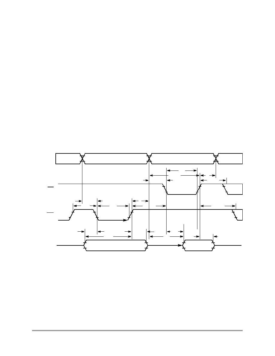
134
56F8346 Technical Data
Preliminary
cycle at XTAL. DCAOE and DCAEO are used to make this duty cycle adjustment where needed.
DCAOE and DCAEO are calculated as follows:
The timing of write cycles is different when WWS = 0 than when WWS > 0. Therefore, some
parameters contain two sets of numbers to account for this difference. Use the "Wait States
Configuration" column of
Table 10-16
to make the appropriate selection.
Figure 10-4 External Memory Interface Timing
Note:
When multiple lines are given for the same wait state configuration, calculate each and then
select the smallest or most negative.
DCAOE =
=
0.5 - MAX XTAL duty cycle, if ZSRC selects prescaler clock and the prescaler is set to
÷
1
0.0 all other cases
DCAEO =
=
MIN XTAL duty cycle - 0.5, if ZSRC selects prescaler clock and the prescaler is set to
÷
1
0.0 all other cases
Example of DCAOE and DCAEO calculation:
Assuming prescaler is set for
÷
1 and prescaler clock is selected by ZSRC, if XTAL duty cycle
ranges between 45% and 60% high;
DCAOE = .50 - .60 = - 0.1
DCAEO = .45 - .50 = - 0.05
t
DRD
t
RDD
t
AD
t
DOH
t
DOS
t
DWR
t
RDWR
t
WAC
t
WRRD
t
WR
t
AWR
t
WRWR
t
ARDD
t
RDA
t
RDRD
t
RD
t
ARDA
Data Out
Data In
A0-Axx,CS
RD
WR
D0-D15
Note: During read-modify-write instructions and internal instructions, the address lines do not change state.
F
r
e
e
s
c
a
l
e
S
e
m
i
c
o
n
d
u
c
t
o
r
,
I
Freescale Semiconductor, Inc.
For More Information On This Product,
Go to: www.freescale.com
n
c
.
.
.
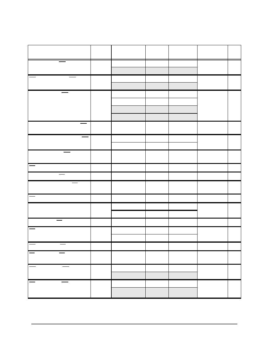
External Memory Interface Timing
56F8346 Technical Data
135
Preliminary
Table 10-16 External Memory Interface Timing
Operating Conditions: V
SS
= V
SSIO
= V
SSA
= 0V, V
DD
= 1.62-1.98V, V
DDIO
= V
DDA
=
3.03.6V, T
A
= 40
°
to +125
°
C, C
L
50pF
Characteristic
Symbol
Wait States
Configuration
D
M
Wait States
Controls
Unit
Address Valid to WR Asserted
t
AWR
WWS=0
-2.121
0.50
WWSS
ns
WWS>0
-1.805
0.75 + DCAOE
WR Width Asserted to WR
Deasserted
t
WR
WWS=0
-0.063
0.25 + DCAOE
WWS
ns
WWS>0
-0.253
1.00
Data Out Valid to WR Asserted
t
DWR
WWS=0
-10.252
0.25 + DCAEO
WWSS
ns
WWS=0
-2.868
0.00
WWS>0
-9.505
0.50
WWS>0
-2.552
0.25 + DCAOE
Valid Data Out Hold Time after WR
Deasserted
t
DOH
-1.512
0.25 + DCAEO
WWSH
ns
Valid Data Out Set Up Time to WR
Deasserted
t
DOS
-2.047
0.25 + DCAOE
WWS,WWSS
ns
-9.000
0.50
Valid Address after WR
Deasserted
t
WAC
-3.888
0.25 + DCAEO
WWSH
ns
RD Deasserted to Address Invalid
t
RDA
-2.922
0.00
RWSH
ns
Address Valid to RD Deasserted
t
ARDD
-1.645
1.00
RWSS,RWS
ns
Valid Input Data Hold after RD
Deasserted
t
DRD
0.00
N/A
1
1.N/A, since device captures data before it deasserts RD
--
ns
RD Assertion Width
t
RD
0.257
1.00
RWS
ns
Address Valid to Input Data Valid
t
AD
-14.414
1.00
RWSS,RWS
ns
-19.299
1.25 + DCAOE
Address Valid to RD Asserted
t
ARDA
-2.002
0.00
RWSS
ns
RD Asserted to Input Data Valid
t
RDD
-12.411
1.00
RWSS,RWS
ns
-17.297
1.25 + DCAOE
WR Deasserted to RD Asserted
t
WRRD
-1.323
0.25 + DCAEO WWSH,RWSS
ns
RD Deasserted to RD Asserted
t
RDRD
-0.357
2
2.If RWSS = RWSH = 0, RD does not deassert during back-to-back reads and D = 0.00 should be used.
0.00
RWSS,RWSH
MDAR
3
3.Substitute BMDAR for MDAR if there is no chip select
ns
WR Deasserted to WR Asserted
t
WRWR
WWS=0
-1.442
0.75 + DCAEO
WWSS,
WWSH
ns
WWS>0
-0.695
1.00
RD Deasserted to WR Asserted
t
RDWR
WWS=0
-0.476
0.50
RWSH,
WWSS,
MDAR
3
ns
WWS>0
-0.160
0.75 + DCAOE
F
r
e
e
s
c
a
l
e
S
e
m
i
c
o
n
d
u
c
t
o
r
,
I
Freescale Semiconductor, Inc.
For More Information On This Product,
Go to: www.freescale.com
n
c
.
.
.
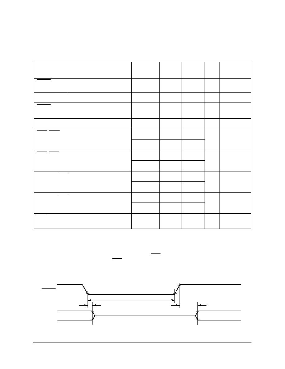
136
56F8346 Technical Data
Preliminary
10.10 Reset, Stop, Wait, Mode Select, and Interrupt Timing
Figure 10-5 Asynchronous Reset Timing
Table 10-17 Reset, Stop, Wait, Mode Select, and Interrupt Timing
1,2
1.
In the formulas, T = clock cycle. For an operating frequency of 60MHz, T = 16.67ns. At 8MHz (used during Reset and
Stop modes), T = 125ns.
2.
Parameters listed are guaranteed by design.
Characteristic
Symbol
Typical
Min
Typical
Max
Unit
See Figure
RESET Assertion to Address, Data and Control
Signals High Impedance
t
RAZ
--
21
ns
10-5
Minimum RESET Assertion Duration
t
RA
16T
--
ns
10-5
RESET Deassertion to First External Address
Output
3
3.
During Power-On Reset, it is possible to use the 56F8346 internal reset stretching circuitry to extend this period to 2
21
T.
t
RDA
63T
64T
ns
10-5
Edge-sensitive Interrupt Request Width
t
IRW
1.5T
--
ns
10-6
IRQA, IRQB Assertion to External Data Memory
Access Out Valid, caused by first instruction
execution in the interrupt service routine
t
IDM
18
--
ns
10-7
t
IDM - FAST
14
--
IRQA, IRQB Assertion to General Purpose Output
Valid, caused by first instruction execution in the
interrupt service routine
t
IG
18
--
ns
10-7
t
IG - FAST
14
--
Delay from IRQA Assertion (exiting Wait) to
External Data Memory access
4
4.
The minimum is specified for the duration of an edge-sensitive IRQA interrupt required to recover from the Stop state.
This is not the minimum required so that the IRQA interrupt is accepted.
t
IRI
22
--
ns
10-8
t
IRI - FAST
18
--
Delay from IRQA Assertion to External Data
Memory Access (exiting Stop)
t
IF
22
--
ns
10-9
t
IF - FAST
18
--
IRQA Width Assertion to Recover from Stop
State
5
5.
The interrupt instruction fetch is visible on the pins only in Mode 3.
t
IW
1.5T
--
ns
10-9
First Fetch
t
RA
t
RAZ
t
RDA
A0A15,
D0D15
RESET
F
r
e
e
s
c
a
l
e
S
e
m
i
c
o
n
d
u
c
t
o
r
,
I
Freescale Semiconductor, Inc.
For More Information On This Product,
Go to: www.freescale.com
n
c
.
.
.
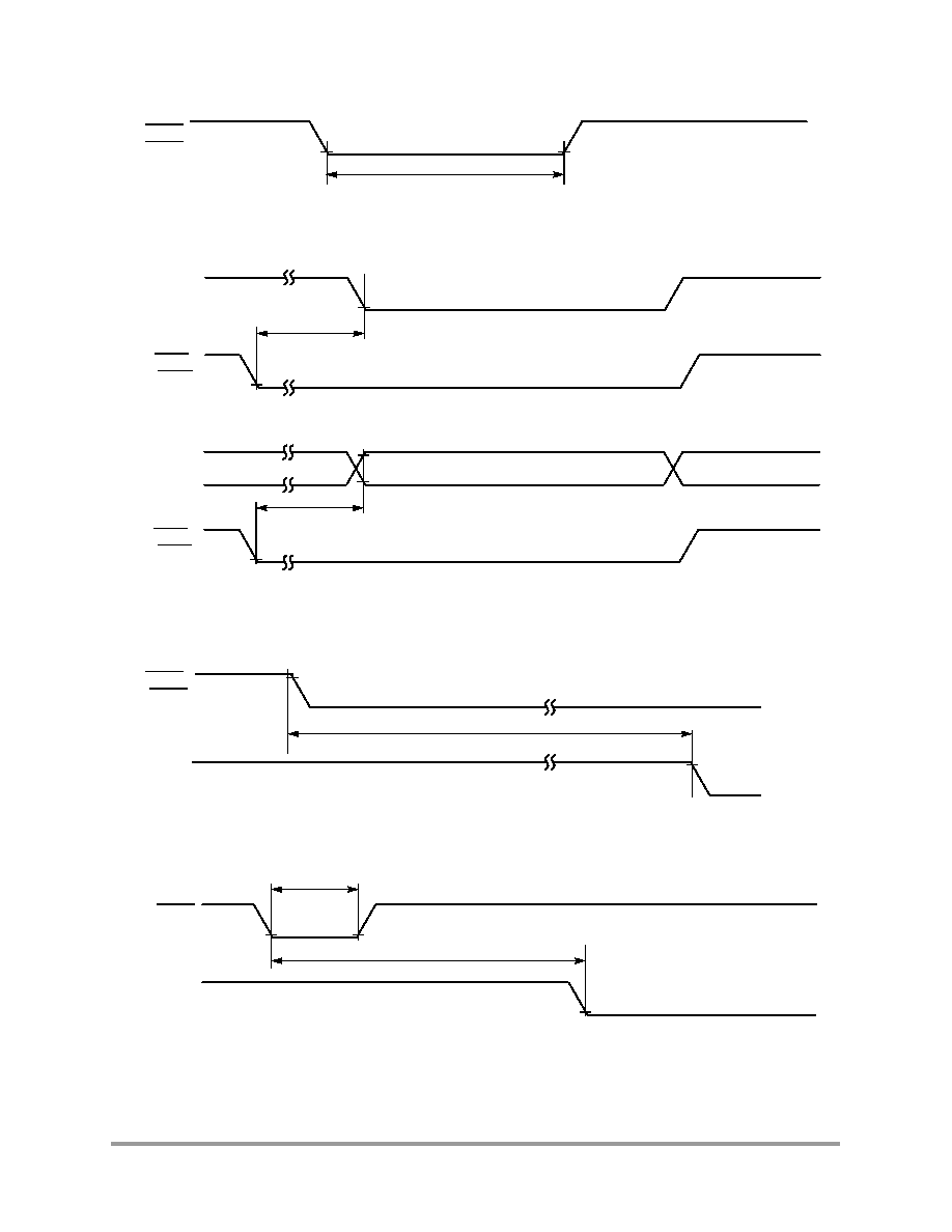
Reset, Stop, Wait, Mode Select, and Interrupt Timing
56F8346 Technical Data
137
Preliminary
Figure 10-6 External Interrupt Timing (Negative Edge-Sensitive)
Figure 10-7 External Level-Sensitive Interrupt Timing
Figure 10-8 Interrupt from Wait State Timing
Figure 10-9 Recovery from Stop State Using Asynchronous Interrupt Timing
IRQA,
IRQB
t
IRW
t
IDM
A0A15
IRQA
,
IRQB
First Interrupt Instruction Execution
a) First Interrupt Instruction Execution
t
IG
General
Purpose
I/O Pin
IRQA
,
IRQB
b) General Purpose I/O
Instruction Fetch
t
IRI
IRQA,
IRQB
First Interrupt Vector
A0A15
Not IRQA Interrupt Vector
t
IW
IRQA
t
IF
A0A15
First Instruction Fetch
F
r
e
e
s
c
a
l
e
S
e
m
i
c
o
n
d
u
c
t
o
r
,
I
Freescale Semiconductor, Inc.
For More Information On This Product,
Go to: www.freescale.com
n
c
.
.
.

138
56F8346 Technical Data
Preliminary
10.11 Serial Peripheral Interface (SPI) Timing
Table 10-18 SPI Timing
1
1.
Parameters listed are guaranteed by design.
Characteristic
Symbol
Min
Max
Unit
See Figure
Cycle time
Master
Slave
t
C
50
50
--
--
ns
ns
10-10
,
10-11
,
10-12
,
10-13
Enable lead time
Master
Slave
t
ELD
--
25
--
--
ns
ns
10-13
Enable lag time
Master
Slave
t
ELG
--
100
--
--
ns
ns
10-13
Clock (SCK) high time
Master
Slave
t
CH
17.6
25
--
--
ns
ns
10-10
,
10-11
,
10-12
,
10-13
Clock (SCK) low time
Master
Slave
t
CL
24.1
25
--
--
ns
ns
10-13
Data set-up time required for inputs
Master
Slave
t
DS
20
0
--
--
ns
ns
10-10
,
10-11
,
10-12
,
10-13
Data hold time required for inputs
Master
Slave
t
DH
0
2
--
--
ns
ns
10-10
,
10-11
,
10-12
,
10-13
Access time (time to data active from
high-impedance state)
Slave
t
A
4.8
15
ns
10-13
Disable time (hold time to high-impedance state)
Slave
t
D
3.7
15.2
ns
10-13
Data Valid for outputs
Master
Slave (after enable edge)
t
DV
--
--
4.5
20.4
ns
ns
10-10
,
10-11
,
10-12
,
10-13
Data invalid
Master
Slave
t
DI
0
0
--
--
ns
ns
10-10
,
10-11
,
10-12
Rise time
Master
Slave
t
R
--
--
11.5
10.0
ns
ns
10-10
,
10-11
,
10-12
,
10-13
Fall time
Master
Slave
t
F
--
--
9.7
9.0
ns
ns
10-10
,
10-11
,
10-12
,
10-13
F
r
e
e
s
c
a
l
e
S
e
m
i
c
o
n
d
u
c
t
o
r
,
I
Freescale Semiconductor, Inc.
For More Information On This Product,
Go to: www.freescale.com
n
c
.
.
.
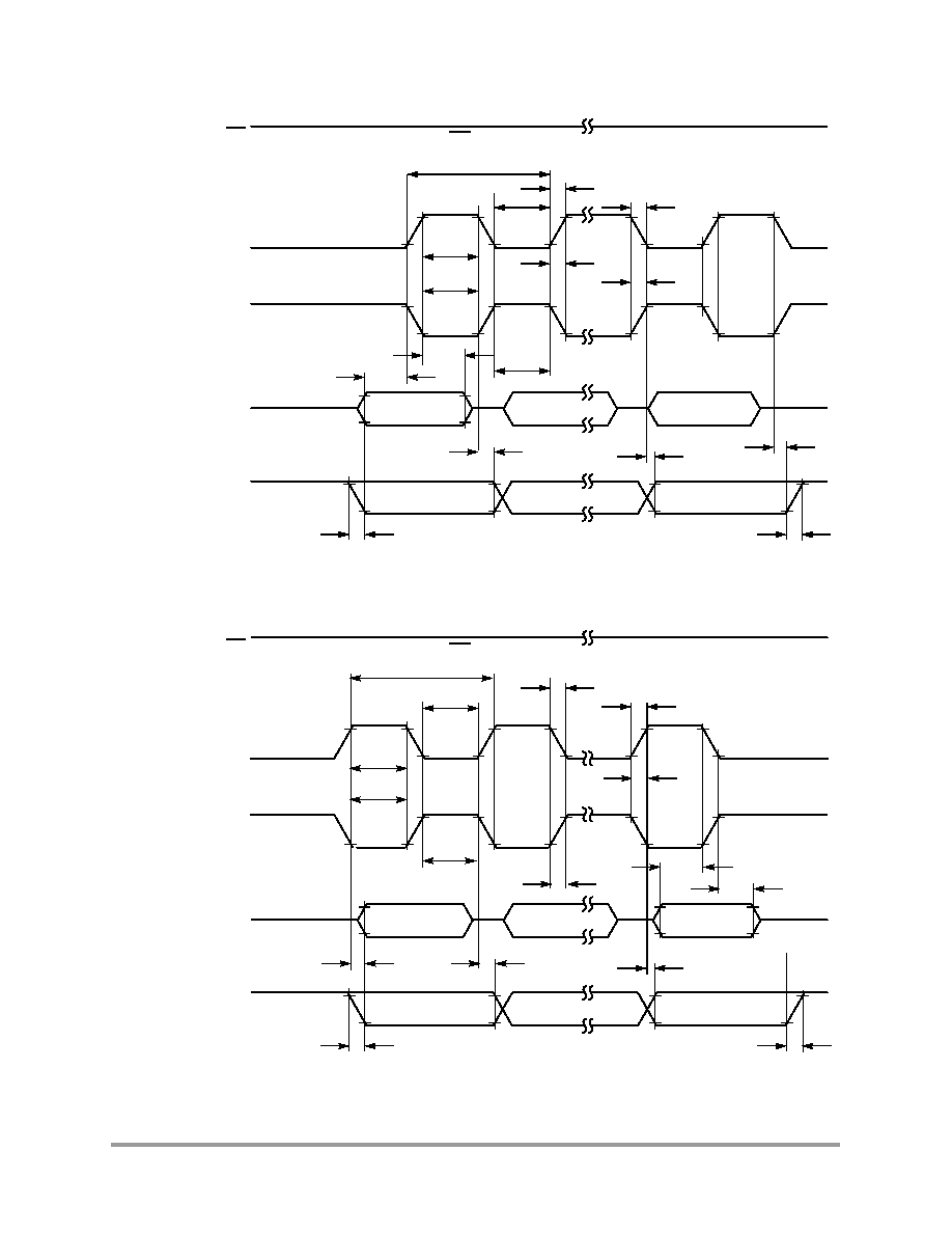
Serial Peripheral Interface (SPI) Timing
56F8346 Technical Data
139
Preliminary
Figure 10-10 SPI Master Timing (CPHA = 0)
Figure 10-11 SPI Master Timing (CPHA = 1)
SCLK (CPOL = 0)
(Output)
SCLK (CPOL = 1)
(Output)
MISO
MOSI
(Output)
MSB in
Bits 141
LSB in
t
F
t
C
t
CL
t
CL
t
R
t
R
t
F
t
DS
t
DH
t
CH
t
DI
t
DV
t
DI
(ref)
t
R
Master MSB out
Bits 14 1
Master LSB out
SS
(Input)
t
CH
SS is held High on master
t
F
(Input)
SCLK (CPOL = 0)
(Output)
SCLK (CPOL = 1)
(Output)
MISO
(Input)
MOSI
(Output)
MSB in
Bits 14 1
LSB in
t
R
t
C
t
CL
t
CL
t
F
t
CH
t
DV
(ref)
t
DV
t
DI
(ref)
t
R
t
F
Master MSB out
Bits 14 1
Master LSB out
SS
(Input)
t
CH
SS is held High on master
t
DS
t
DH
t
DI
t
R
t
F
F
r
e
e
s
c
a
l
e
S
e
m
i
c
o
n
d
u
c
t
o
r
,
I
Freescale Semiconductor, Inc.
For More Information On This Product,
Go to: www.freescale.com
n
c
.
.
.
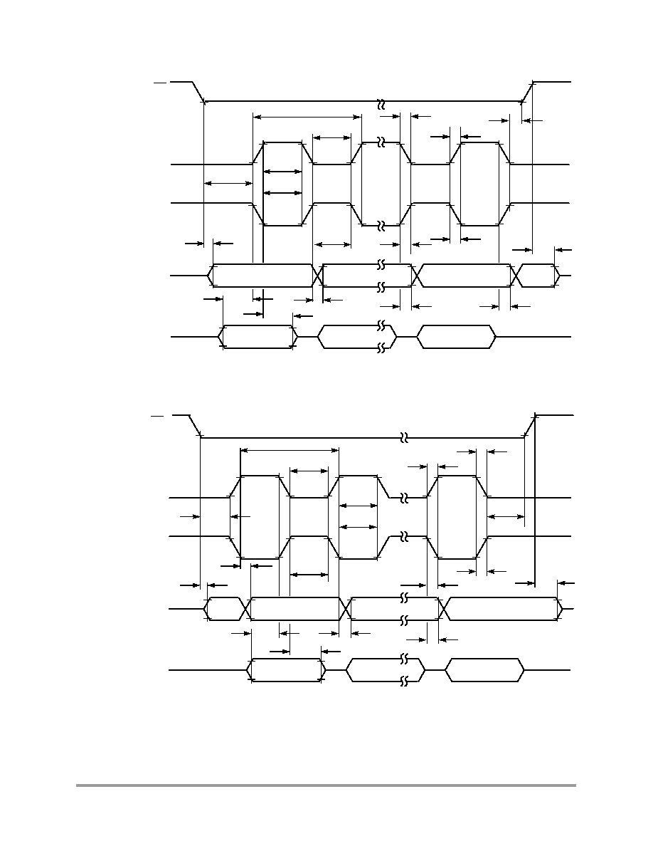
140
56F8346 Technical Data
Preliminary
Figure 10-12 SPI Slave Timing (CPHA = 0)
Figure 10-13 SPI Slave Timing (CPHA = 1)
SCLK (CPOL = 0)
(Input)
SCLK (CPOL = 1)
(Input)
MISO
(Output)
MOSI
(Input)
Slave MSB out
Bits 14 1
t
C
t
CL
t
CL
t
F
t
CH
t
DI
MSB in
Bits 14 1
LSB in
SS
(Input)
t
CH
t
DH
t
R
t
ELG
t
ELD
t
F
Slave LSB out
t
D
t
A
t
DS
t
DV
t
DI
t
R
SCLK (CPOL = 0)
(Input)
SCLK (CPOL = 1)
(Input)
MISO
(Output)
MOSI
(Input)
Slave MSB out
Bits 14 1
t
C
t
CL
t
CL
t
CH
t
DI
MSB in
Bits 14 1
LSB in
SS
(Input)
t
CH
t
DH
t
F
t
R
Slave LSB out
t
D
t
A
t
ELD
t
DV
t
F
t
R
t
ELG
t
DV
t
DS
F
r
e
e
s
c
a
l
e
S
e
m
i
c
o
n
d
u
c
t
o
r
,
I
Freescale Semiconductor, Inc.
For More Information On This Product,
Go to: www.freescale.com
n
c
.
.
.
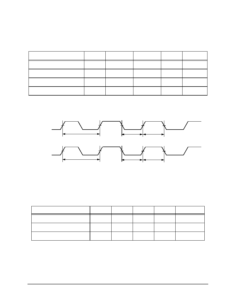
Quad Timer Timing
56F8346 Technical Data
141
Preliminary
10.12 Quad Timer Timing
Figure 10-14 Timer Timing
10.13 Quadrature Decoder Timing
Table 10-19 Timer Timing
1, 2
1.
In the formulas listed, T = the clock cycle. For 60MHz operation, T = 16.67ns.
2.
Parameters listed are guaranteed by design.
Characteristic
Symbol
Min
Max
Unit
See Figure
Timer input period
P
IN
2T + 6
--
ns
10-14
Timer input high / low period
P
INHL
1T + 3
--
ns
10-14
Timer output period
P
OUT
1T - 3
--
ns
10-14
Timer output high / low period
P
OUTHL
0.5T - 3
--
ns
10-14
Table 10-20 Quadrature Decoder Timing
1, 2
1.
In the formulas listed, T = the clock cycle. For 60MHz operation, T=16.67ns.
2.
Parameters listed are guaranteed by design.
Characteristic
Symbol
Min
Max
Unit
See Figure
Quadrature input period
P
IN
4T + 12
--
ns
10-15
Quadrature input high / low period
P
HL
2T + 6
--
ns
10-15
Quadrature phase period
P
PH
1T + 3
--
ns
10-15
P
OUT
P
OUTHL
P
OUTHL
P
IN
P
INHL
P
INHL
Timer Inputs
Timer Outputs
F
r
e
e
s
c
a
l
e
S
e
m
i
c
o
n
d
u
c
t
o
r
,
I
Freescale Semiconductor, Inc.
For More Information On This Product,
Go to: www.freescale.com
n
c
.
.
.
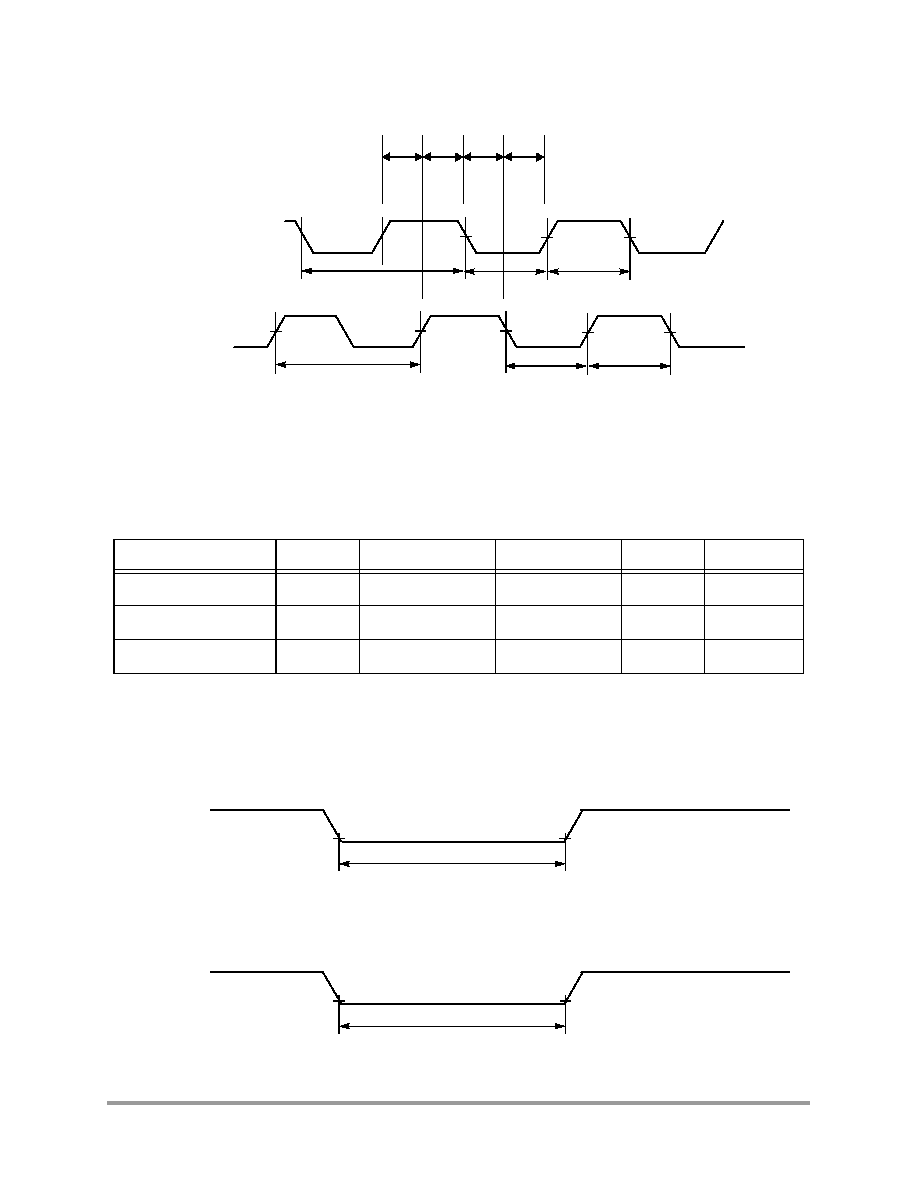
142
56F8346 Technical Data
Preliminary
Figure 10-15 Quadrature Decoder Timing
10.14 Serial Communication Interface (SCI) Timing
Figure 10-16 RXD Pulse Width
Figure 10-17 TXD Pulse Width
Table 10-21 SCI Timing
1
1.
Parameters listed are guaranteed by design.
Characteristic
Symbol
Min
Max
Unit
See Figure
Baud Rate
2
2.
f
MAX
is the frequency of operation of the system clock, ZCLK, in MHz, which is 60MHz for the 56F8346 device.
BR
--
(f
MAX
/16)
Mbps
--
RXD
3
Pulse Width
3.
The RXD pin in SCI0 is named RXD0 and the RXD pin in SCI1 is named RXD1.
RXD
PW
0.965/BR
1.04/BR
ns
10-16
TXD
4
Pulse Width
4.
The TXD pin in SCI0 is named TXD0 and the TXD pin in SCI1 is named TXD1.
TXD
PW
0.965/BR
1.04/BR
ns
10-17
Phase B
(Input)
P
IN
P
HL
P
HL
Phase A
(Input)
P
IN
P
HL
P
HL
P
PH
P
PH
P
PH
P
PH
RXD
PW
RXD
SCI receive
data pin
(Input)
TXD
PW
TXD
SCI receive
data pin
(Input)
F
r
e
e
s
c
a
l
e
S
e
m
i
c
o
n
d
u
c
t
o
r
,
I
Freescale Semiconductor, Inc.
For More Information On This Product,
Go to: www.freescale.com
n
c
.
.
.
Controller Area Network (CAN) Timing
56F8346 Technical Data
143
Preliminary
10.15 Controller Area Network (CAN) Timing
Figure 10-18 Bus Wake Up Detection
10.16 JTAG Timing
Table 10-22 CAN Timing
1
1.
Parameters listed are guaranteed by design
Characteristic
Symbol
Min
Max
Unit
See Figure
Baud Rate
BR
CAN
--
1
Mbps
--
Bus Wake Up detection
T
WAKEUP
5
--
µ
s
10-18
Table 10-23 JTAG Timing
Characteristic
Symbol
Min
Max
Unit
See Figure
TCK frequency of operation
using EOnCE
1
1.
TCK frequency of operation must be less than 1/8 the processor rate.
f
OP
DC
SYS_CLK/8
MHz
10-19
TCK frequency of operation not
using EOnCE
1
f
OP
DC
SYS_CLK/4
MHz
10-19
TCK clock pulse width
t
PW
50
--
ns
10-19
TMS, TDI data set-up time
t
DS
5
--
ns
10-20
TMS, TDI data hold time
t
DH
5
--
ns
10-20
TCK low to TDO data valid
t
DV
--
30
ns
10-20
TCK low to TDO tri-state
t
TS
--
30
ns
10-20
TRST assertion time
t
TRST
2T
2
2.
T = processor clock period (nominally 1/60MHz)
--
ns
10-21
T
WAKEUP
CAN_RX
CAN receive
data pin
(Input)
F
r
e
e
s
c
a
l
e
S
e
m
i
c
o
n
d
u
c
t
o
r
,
I
Freescale Semiconductor, Inc.
For More Information On This Product,
Go to: www.freescale.com
n
c
.
.
.
144
56F8346 Technical Data
Preliminary
Figure 10-19 Test Clock Input Timing Diagram
Figure 10-20 Test Access Port Timing Diagram
Figure 10-21 TRST Timing Diagram
TCK
(Input)
V
M
V
IL
V
M
= V
IL
+ (V
IH
V
IL
)/2
t
PW
1/f
OP
t
PW
V
M
V
IH
Input Data Valid
Output Data Valid
Output Data Valid
t
DS
t
DH
t
DV
t
TS
t
DV
TCK
(Input)
TDI
(Input)
TDO
(Output)
TDO
(Output
)
TDO
(Output)
TMS
TRST
(Input)
t
TRST
F
r
e
e
s
c
a
l
e
S
e
m
i
c
o
n
d
u
c
t
o
r
,
I
Freescale Semiconductor, Inc.
For More Information On This Product,
Go to: www.freescale.com
n
c
.
.
.

Analog-to-Digital Converter (ADC) Parameters
56F8346 Technical Data
145
Preliminary
10.17 Analog-to-Digital Converter (ADC) Parameters
Table 10-24 ADC Parameters
Characteristic
Symbol
Min
Typ
Max
Unit
Input voltages
V
ADIN
V
REFL
--
V
REFH
V
Resolution
R
ES
12
--
12
Bits
Integral Non-Linearity
1
INL
+/- 1
+/- 2.4
+/- 3.2
LSB
2
Differential Non-Linearity
DNL
> -1
+/- 0.7
< +1
LSB
2
Monotonicity
GUARANTEED
ADC internal clock
f
ADIC
0.5
--
5
MHz
Conversion range
R
AD
V
REFL
--
V
REFH
V
ADC channel power-up time
t
ADPU
5
6
16
t
AIC
cycles
3
ADC reference circuit power-up time
4
t
VREF
--
--
25
ms
Conversion time
t
ADC
--
6
--
t
AIC
cycles
3
Sample time
t
ADS
--
1
--
t
AIC
cycles
3
Input capacitance
C
ADI
--
5
--
pF
Input injection current
5
, per pin
I
ADI
--
--
3
mA
Input injection current, total
I
ADIT
--
--
20
mA
V
REFH
current
I
VREFH
--
1.2
3
mA
ADC A current
I
ADCA
--
25
--
mA
ADC B current
I
ADCB
--
25
--
mA
Quiescent current
I
ADCQ
--
0
10
µ
A
Uncalibrated Gain Error
E
GAIN
.99
.996 to 1.004
1.01
--
Uncalibrated Offset Voltage
V
OFFSET
--
+/- 18
+/- 30
mV
Calibrated Absolute Error
6
AE
CAL
--
See
Figure 10-22
--
LSBs
Calibration Factor 1
7
CF1
--
-0.003141
--
--
Calibration Factor 2
7
CF2
--
-17.6
--
--
Crosstalk between channels
--
--
-60
--
dB
Common Mode Voltage
V
common
--
(V
REFH
- V
REFLO
) / 2
--
V
Signal-to-noise ratio
SNR
--
64.6
--
db
Signal-to-noise plus distortion ratio
SINAD
--
59.1
--
db
Total Harmonic Distortion
THD
--
60.6
--
db
Spurious Free Dynamic Range
SFDR
--
61.1
--
db
Effective Number Of Bits
8
ENOB
--
9.6
--
Bits
F
r
e
e
s
c
a
l
e
S
e
m
i
c
o
n
d
u
c
t
o
r
,
I
Freescale Semiconductor, Inc.
For More Information On This Product,
Go to: www.freescale.com
n
c
.
.
.
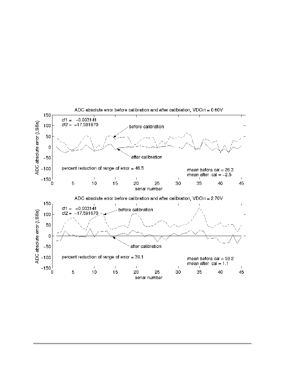
146
56F8346 Technical Data
Preliminary
Figure 10-22 ADC Absolute Error Over Processing and Temperature Extremes
Before and After Calibration for VDC
in
= 0.60V and 2.70V
Note: The absolute error data shown in the graphs above reflects the effects of both gain error and
offset error. The data was taken on 15 parts: three each from four processing corner lots as well as
three from one nominally processed lot, each at three temperatures: -40°C, 27°C, and 150°C (giving
the 45 data points shown above), for two input DC voltages: 0.60V and 2.70V. The data indicates
1.
INL measured from V
in
= .1V
REFH
to V
in
= .9V
REFH
10% to 90% Input Signal Range
2.
LSB = Least Significant Bit
3.
ADC clock cycles
4.
Assumes each voltage reference pin is bypassed with 0.1
µ
F ceramic capacitors to ground
5.
The current that can be injected or sourced from an unselected ADC signal input without impacting the performance of
the ADC. This allows the ADC to operate in noisy industrial environments where inductive flyback is possible.
6.
Absolute error includes the effects of both gain error and offset error.
7.
Please see the 56F8300 Peripheral User's Manual for additional information on ADC calibration.
8.
ENOB = (SINAD - 1.76)/6.02
F
r
e
e
s
c
a
l
e
S
e
m
i
c
o
n
d
u
c
t
o
r
,
I
Freescale Semiconductor, Inc.
For More Information On This Product,
Go to: www.freescale.com
n
c
.
.
.
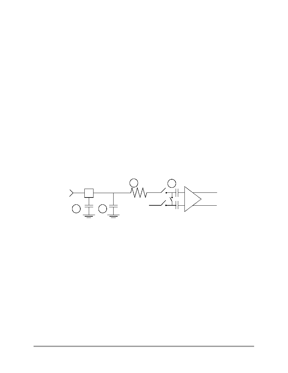
Equivalent Circuit for ADC Inputs
56F8346 Technical Data
147
Preliminary
that for the given population of parts, calibration significantly reduced (by as much as 39%) the
collective variation (spread) of the absolute error of the population. It also significantly reduced
(by as much as 80%) the mean (average) of the absolute error and thereby brought it significantly
closer to the ideal value of zero. Although not guaranteed, it is believed that calibration will
produce results similar to those shown above for any population of parts including those which
represent processing and temperature extremes.
10.18 Equivalent Circuit for ADC Inputs
Figure 10-23
illustrates the ADC input circuit during sample and hold. S1 and S2 are always
open/closed at the same time that S3 is closed/open. When S1/S2 are closed & S3 is open, one input
of the sample and hold circuit moves to V
REFH
- V
REFH
/ 2, while the other charges to the analog
input voltage. When the switches are flipped, the charge on C1 and C2 are averaged via S3, with
the result that a single-ended analog input is switched to a differential voltage centered about
V
REFH
- V
REFH
/ 2. The switches switch on every cycle of the ADC clock (open one-half ADC
clock, closed one-half ADC clock). Note that there are additional capacitances associated with the
analog input pad, routing, etc., but these do not filter into the S/H output voltage, as S1 provides
isolation during the charge-sharing phase.
One aspect of this circuit is that there is an on-going input current, which is a function of the analog
input voltage, V
REF
and the ADC clock frequency.
1.
Parasitic capacitance due to package, pin-to-pin and pin-to-package base coupling; 1.8pf
2.
Parasitic capacitance due to the chip bond pad, ESD protection devices and signal routing; 2.04pf
3.
Equivalent resistance for the ESD isolation resistor and the channel select mux; 500 ohms
4.
Sampling capacitor at the sample and hold circuit. Capacitor C1 is normally disconnected from the input and is
only connected to it at sampling time; 1pf
Figure 10-23 Equivalent Circuit for A/D Loading
10.19 Power Consumption
This section provides additional detail which can be used to optimize power consumption for a
given application.
Power consumption is given by the following equation:
Total power =
A: internal [static component]
+ B: internal [state-dependent component]
+ C: internal [dynamic component]
+ D: external [dynamic component]
+ E: external [static]
1
2
3
Analog Input
4
S1
S2
S3
C1
C2
S/H
C1 = C2 = 1pF
(V
REFH
- V
REFLO
) / 2
F
r
e
e
s
c
a
l
e
S
e
m
i
c
o
n
d
u
c
t
o
r
,
I
Freescale Semiconductor, Inc.
For More Information On This Product,
Go to: www.freescale.com
n
c
.
.
.

148
56F8346 Technical Data
Preliminary
A, the internal [static component], is comprised of the DC bias currents for the oscillator, leakage
current, PLL, and voltage references. These sources operate independently of processor state or
operating frequency.
B, the internal [state-dependent component], reflects the supply current required by certain on-chip
resources only when those resources are in use. These include RAM, Flash memory and the ADCs.
C, the internal [dynamic component], is classic C*V
2
*F CMOS power dissipation corresponding
to the 56800E core and standard cell logic.
D, the external [dynamic component], reflects power dissipated on-chip as a result of capacitive
loading on the external pins of the chip. This is also commonly described as C*V
2
*F, although
simulations on two of the IO cell types used on the 56F8346 reveal that the power-versus-load
curve does have a non-zero Y-intercept.
Power due to capacitive loading on output pins is (first order) a function of the capacitive load and
frequency at which the outputs change.
Table 10-25
provides coefficients for calculating power
dissipated in the IO cells as a function of capacitive load. In these cases:
TotalPower =
((Intercept +Slope*Cload)*frequency/10MHz)
where:
·
Summation is performed over all output pins with capacitive loads
·
TotalPower is expressed in mW
·
Cload is expressed in pF
Because of the low duty cycle on most device pins, power dissipation due to capacitive loads was
found to be fairly low when averaged over a period of time. The one possible exception to this is
if the chip is using the external address and data buses at a rate approaching the maximum system
rate. In this case, power from these buses can be significant.
E, the external [static component], reflects the effects of placing resistive loads on the outputs of
the device. Sum the total of all V
2
/R or IV to arrive at the resistive load contribution to power.
Assume V = 0.5 for the purposes of these rough calculations. For instance, if there is a total of 8
PWM outputs driving 10mA into LEDs, then P = 8*.5*.01 = 40mW.
In previous discussions, power consumption due to parasitics associated with pure input pins is
ignored, as it is assumed to be negligible.
Table 10-25 IO Loading Coefficients at 10MHz
Intercept
Slope
PDU08DGZ_ME
1.3
0.11mW / pF
PDU04DGZ_ME
1.15mW
0.11mW / pF
F
r
e
e
s
c
a
l
e
S
e
m
i
c
o
n
d
u
c
t
o
r
,
I
Freescale Semiconductor, Inc.
For More Information On This Product,
Go to: www.freescale.com
n
c
.
.
.
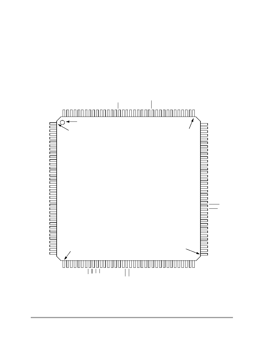
Package and Pin-Out Information 56F8346
56F8346 Technical Data
149
Preliminary
Part 11 Packaging
11.1 Package and Pin-Out Information 56F8346
This section contains package and pin-out information for the 56F8346. This device comes in a
144-pin Low-profile Quad Flat Pack (LQFP).
Figure 11-1
shows the package outline for the
LQFP;
Figure 11-2
shows the mechanical parameters for this package, and
Table 11-1
lists the
pin-out for the 144-pin LQFP.
Figure 11-1 Top View, 56F8346 144-Pin LQFP Package
V
DD_IO
V
PP
2
CLKO
TXD0
RXD0
PHASEA1
PHASEB1
INDEX1
HOME1
A1
A2
A3
A4
A5
V
CAP
4
V
DD_IO
A6
A7
A8
A9
A10
A11
A12
A13
A14
A15
V
SS
D7
D8
D9
V
DD_IO
D10
GPIOB0
PWMB0
PWMB1
PWMB2
V
SS
V
DD_
I
O
PWM
B
3
PW
M
B4
PWM
B
5
TX
D
1
RX
D1
WR
RD
PS
DS
GP
IO
D
0
GP
IO
D1
I
SB0
V
CA
P
1
I
SB1
I
SB2
IRQA
IRQB
FA
U
L
T
B
0
FA
U
L
T
B
1
FA
U
L
T
B
2
D0
D1
FA
U
L
T
B
3
PWM
A
0
V
SS
PWM
A
1
PW
M
A2
V
DD
_
I
O
PWM
A
3
PWM
A
4
V
SS
PWM
A
5
FA
U
L
TA
0
D2
FAULTA1
FAULTA2
D3
D4
D5
D6
OCR_DIS
V
DDA_OSC_PLL
XTAL
EXTAL
V
CAP
3
V
DD_IO
RSTO
RESET
CLKMODE
ANA0
ANA1
ANA2
ANA3
ANA4
ANA5
ANA6
ANA7
Temp_Sense
V
REFLO
V
REFN
V
REFMID
V
REFP
V
REFH
V
DDA_ADC
V
SSA_ADC
ANB0
ANB1
ANB2
ANB3
ANB4
ANB5
ANB6
ANB7
EXTBO
O
T
I
SA0
I
SA1
IS
A
2
TD
0
TD
1
TC
0
V
DD
_
I
O
TR
ST
TC
K
TMS
TD
I
TD
O
V
PP
I
CAN_
T
X
CAN_
RX
V
CA
P
2
SS0
SCL
K
0
MI
S
O
0
MO
S
I
0
D1
1
D1
2
D1
3
D1
4
D1
5
A0
PHASEA0
PHASEB0
I
NDEX0
HOM
E
0
EM
I
_
M
O
DE
V
SS
Motorola
56F8346
Pin 1
Orientation Mark
73
109
37
F
r
e
e
s
c
a
l
e
S
e
m
i
c
o
n
d
u
c
t
o
r
,
I
Freescale Semiconductor, Inc.
For More Information On This Product,
Go to: www.freescale.com
n
c
.
.
.

150
56F8346 Technical Data
Preliminary
Table 11-1 56F8346 144-Pin LQFP Package Identification by Pin Number
Pin No.
Signal
Name
Pin No.
Signal Name
Pin No.
Signal Name
Pin No.
Signal Name
1
V
DD_IO
37
V
SS
73
FAULTA1
109
ANB5
2
V
PP
2
38
V
DD_IO
74
FAULTA2
110
ANB6
3
CLKO
39
PWMB3
75
D3
111
ANB7
4
TXD0
40
PWMB4
76
D4
112
EXTBOOT
5
RXD0
41
PWMB5
77
D5
113
ISA0
6
PHASEA1
42
TXD1
78
D6
114
ISA1
7
PHASEB1
43
RXD1
79
OCR_DIS
115
ISA2
8
INDEX1
44
WR
80
V
DDA_OSC_PLL
116
TD0
9
HOME1
45
RD
81
XTAL
117
TD1
10
A1
46
PS
82
EXTAL
118
TC0
11
A2
47
DS
83
V
CAP
3
119
V
DD_IO
12
A3
48
GPIOD0
84
V
DD_IO
120
TRST
13
A4
49
GPIOD1
85
RSTO
121
TCK
14
A5
50
ISB0
86
RESET
122
TMS
15
V
CAP
4
51
V
CAP
1
87
CLKMODE
123
TDI
16
V
DD_IO
52
ISB1
88
ANA0
124
TDO
17
A6
53
ISB2
89
ANA1
125
V
PP
1
18
A7
54
IRQA
90
ANA2
126
CAN_TX
19
A8
55
IRQB
91
ANA3
127
CAN_RX
20
A9
56
FAULTB0
92
ANA4
128
V
CAP
2
21
A10
57
FAULTB1
93
ANA5
129
SS0
22
A11
58
FAULTB2
94
ANA6
130
SCLK0
23
A12
59
D0
95
ANA7
131
MISO0
24
A13
60
D1
96
TEMP_SENSE
132
MOSI0
25
A14
61
FAULTB3
97
V
REFLO
133
D11
26
A15
62
PWMA0
98
V
REFN
134
D12
27
V
SS
63
V
SS
99
V
REFMID
135
D13
F
r
e
e
s
c
a
l
e
S
e
m
i
c
o
n
d
u
c
t
o
r
,
I
Freescale Semiconductor, Inc.
For More Information On This Product,
Go to: www.freescale.com
n
c
.
.
.

Package and Pin-Out Information 56F8346
56F8346 Technical Data
151
Preliminary
28
D7
64
PWMA1
100
V
REFP
136
D14
29
D8
65
PWMA2
101
V
REFH
137
D15
30
D9
66
V
DD_IO
102
V
DDA_ADC
138
A0
31
V
DD_IO
67
PWMA3
103
V
SSA_ADC
139
PHASEA0
32
D10
68
PWMA4
104
ANB0
140
PHASEB0
33
GPIOB0
69
V
SS
105
ANB1
141
INDEX0
34
PWMB0
70
PWMA5
106
ANB2
142
HOME0
35
PWMB1
71
FAULTA0
107
ANB3
143
EMI_MODE
36
PWMB2
72
D2
108
ANB4
144
V
SS
Table 11-1 56F8346 144-Pin LQFP Package Identification by Pin Number
Pin No.
Signal
Name
Pin No.
Signal Name
Pin No.
Signal Name
Pin No.
Signal Name
F
r
e
e
s
c
a
l
e
S
e
m
i
c
o
n
d
u
c
t
o
r
,
I
Freescale Semiconductor, Inc.
For More Information On This Product,
Go to: www.freescale.com
n
c
.
.
.
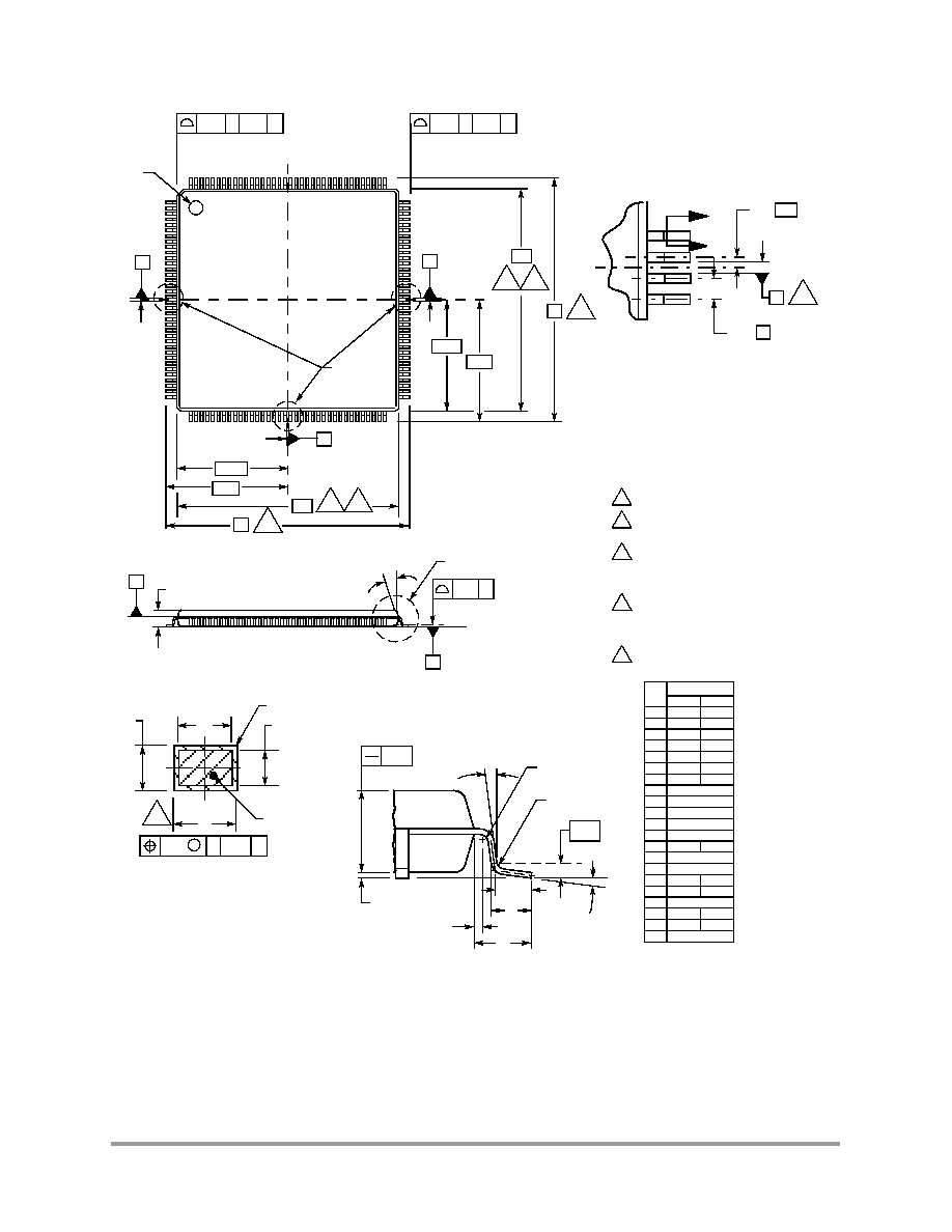
152
56F8346 Technical Data
Preliminary
Figure 11-2 56F8346 144-pin LQFP Mechanical Information
D
0.20 H B-C
144
GAGE PLANE
73
109
37
SEATING
108
1
36
72
PLANE
4X
4X 36 TIPS
PIN 1
INDEX
VIEW A
E1
E1/2
E/2
D1/2
D/2
E
e/2
e
D1
D
0.1
A
2
VIEW B
A
A
140X
4X
VIEW A
PLATING
b1
c1
c
b
BASE
METAL
SECTION A-A
(ROTATED 90 )
144 PLACES
°
D
0.08
M
A B-C
DIM
D1
MIN
MAX
20.00 BSC
MILLIMETERS
E1
20.00 BSC
A
---
1.60
A1
0.05
0.15
A2
1.35
1.45
b
0.17
0.27
L
0.45
0.75
b1
0.17
0.23
e
0.50 BSC
c
0.09
0.20
L2
0.50 REF
R1
0.13
0.20
R2
0.13
---
D
22.00 BSC
E
22.00 BSC
S
0.25 REF
L1
1.00 REF
c1
0.09
0.16
0
7
0
---
1
2
NOTES:
1.
ALL DIMENSIONS ARE IN MILLIMETERS.
2.
INTERPRET DIMENSIONS AND TOLERANCES PER
ASME Y14.5M, 1994.
3.
DATUMS B, C AND D TO BE DETERMINED AT DATUM
H.
4.
THE TOP PACKAGE BODY SIZE MAY BE SMALLER
THAN THE BOTTOM PACKAGE SIZE BY A MAXIMUM
OF 0.1 mm.
5.
DIMENSIONS D1 AND E1 DO NOT INCLUDE MOLD
PROTRUSIONS. THE MAXIMUM ALLOWABLE
PROTRUSION IS 0.25 mm PER SIDE. D1 AND E1 ARE
MAXIMUM BODY SIZE DIMENSIONS INCLUDING MOLD
MISMATCH.
6.
DIMENSION b DOES NOT INCLUDE DAMBAR
PROTRUSION. PROTRUSIONS SHALL NOT CAUSE
THE LEAD WIDTH TO EXCEED 0.35. MINIMUM SPACE
BETWEEN PROTRUSION AND AN ADJACENT LEAD
SHALL BE 0.07 mm.
7.
DIMENSIONS D AND E TO BE DETERMINED AT THE
SEATING PLANE, DATUM A.
CASE 918-03
ISSUE D
DATE 08/22/00
°
°
°
°
0.05
C
L
L1
R2
L
A2
S
R1
L2
A1
1
0.25
VIEW B
D
0.20 A B-C
C
B
D
A
A
144X
X
X=B, C or D
8X
12 REF
4
TOP VIEW
5
7
4
5
7
SIDE VIEW
H
6
3
F
r
e
e
s
c
a
l
e
S
e
m
i
c
o
n
d
u
c
t
o
r
,
I
Freescale Semiconductor, Inc.
For More Information On This Product,
Go to: www.freescale.com
n
c
.
.
.

Thermal Design Considerations
56F8346 Technical Data
153
Preliminary
Part 12 Design Considerations
12.1 Thermal Design Considerations
An estimation of the chip junction temperature, T
J
, can be obtained from the equation:
T
J
= T
A
+ (R
J
x
P
D
)
where:
The junction-to-ambient thermal resistance is an industry-standard value that provides a quick and
easy estimation of thermal performance. Unfortunately, there are two values in common usage: the
value determined on a single-layer board and the value obtained on a board with two planes. For
packages such as the PBGA, these values can be different by a factor of two. Which value is closer
to the application depends on the power dissipated by other components on the board. The value
obtained on a single-layer board is appropriate for the tightly packed printed circuit board. The
value obtained on the board with the internal planes is usually appropriate if the board has
low-power dissipation and the components are well separated.
When a heat sink is used, the thermal resistance is expressed as the sum of a junction-to-case
thermal resistance and a case-to-ambient thermal resistance:
R
J
=
R
J
+
R
C
where:
R
JC
is device-related and cannot be influenced by the user. The user controls the thermal
environment to change the case-to-ambient thermal resistance, R
CA
. For instance, the user can
change the size of the heat sink, the air flow around the device, the interface material, the mounting
arrangement on printed circuit board, or change the thermal dissipation on the printed circuit board
surrounding the device.
To determine the junction temperature of the device in the application when heat sinks are not used,
the Thermal Characterization Parameter (
JT
) can be used to determine the junction temperature
with a measurement of the temperature at the top center of the package case using the following
equation:
T
J
= T
T
+ (
JT
x P
D
)
where:
T
A
= Ambient temperature for the package (
o
C)
R
J
= Junction-to-ambient thermal resistance (
o
C/W)
P
D
= Power dissipation in the package (W)
R
JA
= Package junction-to-ambient thermal resistance °C/W
R
JC
= Package junction-to-case thermal resistance °C/W
R
CA
= Package case-to-ambient thermal resistance °C/W
T
T
=
Thermocouple temperature on top of package (
o
C)
JT
=
Thermal characterization parameter (
o
C)/W
P
D
=
Power dissipation in package (W)
F
r
e
e
s
c
a
l
e
S
e
m
i
c
o
n
d
u
c
t
o
r
,
I
Freescale Semiconductor, Inc.
For More Information On This Product,
Go to: www.freescale.com
n
c
.
.
.

154
56F8346 Technical Data
Preliminary
The thermal characterization parameter is measured per JESD51-2 specification using a 40-gauge
type T thermocouple epoxied to the top center of the package case. The thermocouple should be
positioned so that the thermocouple junction rests on the package. A small amount of epoxy is
placed over the thermocouple junction and over about 1mm of wire extending from the junction.
The thermocouple wire is placed flat against the package case to avoid measurement errors caused
by cooling effects of the thermocouple wire.
When heat sink is used, the junction temperature is determined from a thermocouple inserted at the
interface between the case of the package and the interface material. A clearance slot or hole is
normally required in the heat sink. Minimizing the size of the clearance is important to minimize
the change in thermal performance caused by removing part of the thermal interface to the heat
sink. Because of the experimental difficulties with this technique, many engineers measure the heat
sink temperature and then back-calculate the case temperature using a separate measurement of the
thermal resistance of the interface. From this case temperature, the junction temperature is
determined from the junction-to-case thermal resistance.
12.2 Electrical Design Considerations
Use the following list of considerations to assure correct device operation:
·
Provide a low-impedance path from the board power supply to each V
DD
pin on the device, and
from the board ground to each V
SS
(GND) pin
·
The minimum bypass requirement is to place six 0.010.1
µ
F capacitors positioned as close as
possible to the package supply pins. The recommended bypass configuration is to place one bypass
capacitor on each of the V
DD
/V
SS
pairs, including V
DDA
/V
SSA.
Ceramic and tantalum capacitors
tend to provide better performance tolerances.
·
Ensure that capacitor leads and associated printed circuit traces that connect to the chip V
DD
and
V
SS
(GND)
pins are less than 0.5 inch per capacitor lead
·
Use at least a four-layer Printed Circuit Board (PCB) with two inner layers for V
DD
and V
SS
·
Bypass the V
DD
and V
SS
layers of the PCB with approximately 100
µ
F, preferably with a
high-grade capacitor such as a tantalum capacitor
·
Because the 56F8346's output signals have fast rise and fall times, PCB trace lengths should be
minimal
CAUTION
This device contains protective circuitry to guard
against damage due to high static voltage or electrical
fields. However, normal precautions are advised to
avoid application of any voltages higher than
maximum-rated voltages to this high-impedance circuit.
Reliability of operation is enhanced if unused inputs are
tied to an appropriate voltage level.
F
r
e
e
s
c
a
l
e
S
e
m
i
c
o
n
d
u
c
t
o
r
,
I
Freescale Semiconductor, Inc.
For More Information On This Product,
Go to: www.freescale.com
n
c
.
.
.

Power Distribution and I/O Ring Implementation
56F8346 Technical Data
155
Preliminary
·
Consider all device loads as well as parasitic capacitance due to PCB traces when calculating
capacitance. This is especially critical in systems with higher capacitive loads that could create
higher transient currents in the V
DD
and V
SS
circuits.
·
Take special care to minimize noise levels on the V
REF
, V
DDA
and V
SSA
pins
·
Designs that utilize the TRST pin for JTAG port or EOnCE module functionality (such as
development or debugging systems) should allow a means to assert TRST whenever RESET is
asserted, as well as a means to assert TRST independently of RESET. Designs that do not require
debugging functionality, such as consumer products, should tie these pins together.
·
Because the Flash memory is programmed through the JTAG/EOnCE port, the designer should
provide an interface to this port to allow in-circuit Flash programming
12.3 Power Distribution and I/O Ring Implementation
Figure 12-1
illustrates the general power control incorporated in the 56F8346. This chip contains
an internal regulator which cannot be disabled. The regulator takes regulated 3.3V power from the
V
DD_IO
pins and provides 2.5V to the internal logic of the chip. This means the entire part is
powered from the 3.3V supply.
Notes:
·
Flash, RAM and internal logic are powered from the core regulator output
·
V
PP
1 and V
PP
2 are not connected in the customer system
·
All circuitry, analog and digital, shares a common V
SS
bus
Figure 12-1 56F8346 Power Management
REG
CORE
V
CAP
I/O
ADC
V
DD
V
SS
OCS
REG
V
DDA_OSC_PLL
ROSC
V
SSA_ADC
V
DDA_ADC
V
REFH
V
REFP
V
REFMID
V
REFN
V
REFLO
F
r
e
e
s
c
a
l
e
S
e
m
i
c
o
n
d
u
c
t
o
r
,
I
Freescale Semiconductor, Inc.
For More Information On This Product,
Go to: www.freescale.com
n
c
.
.
.

156
56F8346 Technical Data
Preliminary
Part 13 Ordering Information
Table 13-1
lists the pertinent information needed to place an order. Consult a Motorola
Semiconductor sales office or authorized distributor to determine availability and to order parts.
Table 13-1 56F8346 Ordering Information
Part
Supply
Voltage
Package Type
Pin
Count
Frequency
(MHz)
Temperature
Range
Order Number
MC56F8346
3.03.6 V
Low-Profile Quad Flat Pack
(LQFP)
144
60
-40° to + 105° C
MC56F8346VFV60
MC56F8346
3.03.6 V
Low-Profile Quad Flat Pack
(LQFP)
144
60
-40° to + 125° C
MC56F8346MFV60
F
r
e
e
s
c
a
l
e
S
e
m
i
c
o
n
d
u
c
t
o
r
,
I
Freescale Semiconductor, Inc.
For More Information On This Product,
Go to: www.freescale.com
n
c
.
.
.

Power Distribution and I/O Ring Implementation
56F8346 Technical Data
157
Preliminary
F
r
e
e
s
c
a
l
e
S
e
m
i
c
o
n
d
u
c
t
o
r
,
I
Freescale Semiconductor, Inc.
For More Information On This Product,
Go to: www.freescale.com
n
c
.
.
.

158
56F8346 Technical Data
Preliminary
F
r
e
e
s
c
a
l
e
S
e
m
i
c
o
n
d
u
c
t
o
r
,
I
Freescale Semiconductor, Inc.
For More Information On This Product,
Go to: www.freescale.com
n
c
.
.
.

Power Distribution and I/O Ring Implementation
56F8346 Technical Data
159
Preliminary
F
r
e
e
s
c
a
l
e
S
e
m
i
c
o
n
d
u
c
t
o
r
,
I
Freescale Semiconductor, Inc.
For More Information On This Product,
Go to: www.freescale.com
n
c
.
.
.

HOW TO REACH US:
USA/EUROPE/LOCATIONS NOT LISTED:
Motorola Literature Distribution
P.O. Box 5405, Denver, Colorado 80217
1-800-521-6274 or 480-768-2130
JAPAN:
Motorola Japan Ltd.
SPS, Technical Information Center
3-20-1, Minami-Azabu
Minato-ku
Tokyo 106-8573, Japan
81-3-3440-3569
ASIA/PACIFIC:
Motorola Semiconductors H.K. Ltd.
Silicon Harbour Centre
2 Dai King Street
Tai Po Industrial Estate
Tai Po, N.T. Hong Kong
852-26668334
HOME PAGE:
http://motorola.com/semiconductors
Information in this document is provided solely to enable system and software
implementers to use Motorola products. There are no express or implied copyright licenses
granted hereunder to design or fabricate any integrated circuits or integrated circuits based
on the information in this document.
Motorola reserves the right to make changes without further notice to any products herein.
Motorola makes no warranty, representation or guarantee regarding the suitability of its
products for any particular purpose, nor does Motorola assume any liability arising out of
the application or use of any product or circuit, and specifically disclaims any and all
liability, including without limitation consequential or incidental damages. "Typical"
parameters which may be provided in Motorola data sheets and/or specifications can and
do vary in different applications and actual performance may vary over time. All operating
parameters, including "Typicals" must be validated for each customer application by
customer's technical experts. Motorola does not convey any license under its patent rights
nor the rights of others. Motorola products are not designed, intended, or authorized for use
as components in systems intended for surgical implant into the body, or other applications
intended to support or sustain life, or for any other application in which the failure of the
Motorola product could create a situation where personal injury or death may occur. Should
Buyer purchase or use Motorola products for any such unintended or unauthorized
application, Buyer shall indemnify and hold Motorola and its officers, employees,
subsidiaries, affiliates, and distributors harmless against all claims, costs, damages, and
expenses, and reasonable attorney fees arising out of, directly or indirectly, any claim of
personal injury or death associated with such unintended or unauthorized use, even if such
claim alleges that Motorola was negligent regarding the design or manufacture of the part.
Motorola and the Stylized M Logo are registered in the U.S. Patent and Trademark Office.
digital dna is a trademark of Motorola, Inc. This product incorporates SuperFlash®
technology licensed from SST. All other product or service names are the property of their
respective owners. Motorola, Inc. is an Equal Opportunity/Affirmative Action Employer.
© Motorola, Inc. 2004
MC56F8346/D
F
r
e
e
s
c
a
l
e
S
e
m
i
c
o
n
d
u
c
t
o
r
,
I
Freescale Semiconductor, Inc.
For More Information On This Product,
Go to: www.freescale.com
n
c
.
.
.
Document Outline