 | –≠–ª–µ–∫—Ç—Ä–æ–Ω–Ω—ã–π –∫–æ–º–ø–æ–Ω–µ–Ω—Ç: 74173 | –°–∫–∞—á–∞—Ç—å:  PDF PDF  ZIP ZIP |
MOTOROLA
SEMICONDUCTOR TECHNICAL DATA
1
REV 6
©
Motorola, Inc. 1995
10/95
Quad 3-State D Flip-Flop with
Common Clock and Reset
High≠Performance Silicon≠Gate CMOS
The MC74HC173 is identical in pinout to the LS173. The device inputs are
compatible with standard CMOS outputs; with pullup resistors, they are
compatible with LSTTL outputs.
Data, when enabled, are clocked into the four D flip≠flops with the rising
edge of the common Clock. When either or both of the Output Enable
Controls is high, the outputs are in a high≠impedance state. This feature
allows the HC173 to be used in bus≠oriented systems. The Reset feature is
asynchronous and active high.
∑
Output Drive Capability: 15 LSTTL Loads
∑
Outputs Directly Interface to CMOS, NMOS, and TTL
∑
Operating Voltage Range: 2 to 6 V
∑
Low Input Current: 1
µ
A
∑
High Noise Immunity Characteristic of CMOS Devices
∑
In Compliance with the Requirements Defined by JEDEC Standard
No. 7A
∑
Chip Complexity 208 FETs or 52 Equivalent Gates
FUNCTION TABLE
Inputs
Output
Output Enables
Reset
Clock
Data Enables
Data
D
OE1
OE2
Reset
Clock
DE1
DE2
Data
D
Q
L
L
H
X
X
X
X
L
L
L
L
L
X
X
X
No Change
L
L
L
H
X
X
X
No Change
L
L
L
H
X
X
No Change
L
L
L
X
H
X
No Change
L
L
L
L
L
L
L
L
L
L
L
L
H
H
L
L
L
X
X
X
No Change
L
H
X
X
X
X
X
High Impedance
H
L
X
X
X
X
X
High Impedance
H
H
X
X
X
X
X
High Impedance
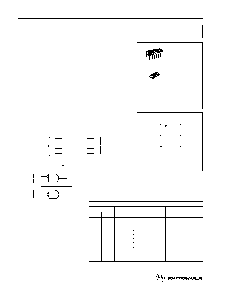
MC74HC173
PIN ASSIGNMENT
13
14
15
16
9
10
11
12
5
4
3
2
1
8
7
6
D2
D1
D0
RESET
VCC
DE1
DE2
D3
Q1
Q0
OE2
OE1
GND
CLOCK
Q3
Q2
D SUFFIX
SOIC PACKAGE
CASE 751B≠05
N SUFFIX
PLASTIC PACKAGE
CASE 648≠08
ORDERING INFORMATION
MC74HCXXXN
MC74HCXXXD
Plastic
SOIC
1
16
1
16
LOGIC DIAGRAM
VCC = PIN 16
GND = PIN 8
DATA
INPUTS
3≠STATE
NONINVERTING
OUTPUTS
D0
D1
D2
D3
14
13
12
11
3
4
5
6
Q0
Q1
Q2
Q3
CLOCK
7
DATA≠
ENABLES
OUTPUT
ENABLES
DE1
DE2
OE1
OE2
RESET
9
10
15
1
2
MC74HC173
MOTOROLA
High≠Speed CMOS Logic Data
DL129 -- Rev 6
2
ŒŒŒŒŒŒŒŒŒŒŒŒŒŒŒŒŒŒŒŒŒŒŒ
ŒŒŒŒŒŒŒŒŒŒŒŒŒŒŒŒŒŒŒŒŒŒŒ
ŒŒŒŒŒŒŒŒŒŒŒŒŒŒŒŒŒŒŒŒŒŒŒ
ŒŒŒŒŒŒŒŒŒŒŒŒŒŒŒŒŒŒŒŒŒŒŒ
MAXIMUM RATINGS*
ŒŒŒ
ŒŒŒ
ŒŒŒ
ŒŒŒ
Symbol
ŒŒŒŒŒŒŒŒŒŒŒŒŒŒ
ŒŒŒŒŒŒŒŒŒŒŒŒŒŒ
ŒŒŒŒŒŒŒŒŒŒŒŒŒŒ
ŒŒŒŒŒŒŒŒŒŒŒŒŒŒ
Parameter
ŒŒŒŒŒŒ
ŒŒŒŒŒŒ
ŒŒŒŒŒŒ
ŒŒŒŒŒŒ
Value
ŒŒŒ
ŒŒŒ
ŒŒŒ
ŒŒŒ
Unit
ŒŒŒ
ŒŒŒ
ŒŒŒ
ŒŒŒ
VCC
ŒŒŒŒŒŒŒŒŒŒŒŒŒŒ
ŒŒŒŒŒŒŒŒŒŒŒŒŒŒ
ŒŒŒŒŒŒŒŒŒŒŒŒŒŒ
ŒŒŒŒŒŒŒŒŒŒŒŒŒŒ
DC Supply Voltage (Referenced to GND)
ŒŒŒŒŒŒ
ŒŒŒŒŒŒ
ŒŒŒŒŒŒ
ŒŒŒŒŒŒ
≠ 0.5 to + 7.0
ŒŒŒ
ŒŒŒ
ŒŒŒ
ŒŒŒ
V
ŒŒŒ
ŒŒŒ
ŒŒŒ
ŒŒŒ
Vin
ŒŒŒŒŒŒŒŒŒŒŒŒŒŒ
ŒŒŒŒŒŒŒŒŒŒŒŒŒŒ
ŒŒŒŒŒŒŒŒŒŒŒŒŒŒ
ŒŒŒŒŒŒŒŒŒŒŒŒŒŒ
DC Input Voltage (Referenced to GND)
ŒŒŒŒŒŒ
ŒŒŒŒŒŒ
ŒŒŒŒŒŒ
ŒŒŒŒŒŒ
≠ 1.5 to VCC + 1.5
ŒŒŒ
ŒŒŒ
ŒŒŒ
ŒŒŒ
V
ŒŒŒ
ŒŒŒ
ŒŒŒ
ŒŒŒ
Vout
ŒŒŒŒŒŒŒŒŒŒŒŒŒŒ
ŒŒŒŒŒŒŒŒŒŒŒŒŒŒ
ŒŒŒŒŒŒŒŒŒŒŒŒŒŒ
ŒŒŒŒŒŒŒŒŒŒŒŒŒŒ
DC Output Voltage (Referenced to GND)
ŒŒŒŒŒŒ
ŒŒŒŒŒŒ
ŒŒŒŒŒŒ
ŒŒŒŒŒŒ
≠ 0.5 to VCC + 0.5
ŒŒŒ
ŒŒŒ
ŒŒŒ
ŒŒŒ
V
ŒŒŒ
ŒŒŒ
ŒŒŒ
ŒŒŒ
Iin
ŒŒŒŒŒŒŒŒŒŒŒŒŒŒ
ŒŒŒŒŒŒŒŒŒŒŒŒŒŒ
ŒŒŒŒŒŒŒŒŒŒŒŒŒŒ
ŒŒŒŒŒŒŒŒŒŒŒŒŒŒ
DC Input Current, per Pin
ŒŒŒŒŒŒ
ŒŒŒŒŒŒ
ŒŒŒŒŒŒ
ŒŒŒŒŒŒ
±
20
ŒŒŒ
ŒŒŒ
ŒŒŒ
ŒŒŒ
mA
ŒŒŒ
ŒŒŒ
ŒŒŒ
ŒŒŒ
Iout
ŒŒŒŒŒŒŒŒŒŒŒŒŒŒ
ŒŒŒŒŒŒŒŒŒŒŒŒŒŒ
ŒŒŒŒŒŒŒŒŒŒŒŒŒŒ
ŒŒŒŒŒŒŒŒŒŒŒŒŒŒ
DC Output Current, per Pin
ŒŒŒŒŒŒ
ŒŒŒŒŒŒ
ŒŒŒŒŒŒ
ŒŒŒŒŒŒ
±
35
ŒŒŒ
ŒŒŒ
ŒŒŒ
ŒŒŒ
mA
ŒŒŒ
ŒŒŒ
ŒŒŒ
ŒŒŒ
ICC
ŒŒŒŒŒŒŒŒŒŒŒŒŒŒ
ŒŒŒŒŒŒŒŒŒŒŒŒŒŒ
ŒŒŒŒŒŒŒŒŒŒŒŒŒŒ
ŒŒŒŒŒŒŒŒŒŒŒŒŒŒ
DC Supply Current, VCC and GND Pins
ŒŒŒŒŒŒ
ŒŒŒŒŒŒ
ŒŒŒŒŒŒ
ŒŒŒŒŒŒ
±
75
ŒŒŒ
ŒŒŒ
ŒŒŒ
ŒŒŒ
mA
ŒŒŒ
ŒŒŒ
ŒŒŒ
ŒŒŒ
PD
ŒŒŒŒŒŒŒŒŒŒŒŒŒŒ
ŒŒŒŒŒŒŒŒŒŒŒŒŒŒ
ŒŒŒŒŒŒŒŒŒŒŒŒŒŒ
ŒŒŒŒŒŒŒŒŒŒŒŒŒŒ
Power Dissipation in Still Air
Plastic DIP
SOIC Package
ŒŒŒŒŒŒ
ŒŒŒŒŒŒ
ŒŒŒŒŒŒ
ŒŒŒŒŒŒ
750
500
ŒŒŒ
ŒŒŒ
ŒŒŒ
ŒŒŒ
mW
ŒŒŒ
ŒŒŒ
ŒŒŒ
ŒŒŒ
Tstg
ŒŒŒŒŒŒŒŒŒŒŒŒŒŒ
ŒŒŒŒŒŒŒŒŒŒŒŒŒŒ
ŒŒŒŒŒŒŒŒŒŒŒŒŒŒ
ŒŒŒŒŒŒŒŒŒŒŒŒŒŒ
Storage Temperature
ŒŒŒŒŒŒ
ŒŒŒŒŒŒ
ŒŒŒŒŒŒ
ŒŒŒŒŒŒ
≠ 65 to + 150
ŒŒŒ
ŒŒŒ
ŒŒŒ
ŒŒŒ
_
C
ŒŒŒ
ŒŒŒ
ŒŒŒ
ŒŒŒ
ŒŒŒ
TL
ŒŒŒŒŒŒŒŒŒŒŒŒŒŒ
ŒŒŒŒŒŒŒŒŒŒŒŒŒŒ
ŒŒŒŒŒŒŒŒŒŒŒŒŒŒ
ŒŒŒŒŒŒŒŒŒŒŒŒŒŒ
ŒŒŒŒŒŒŒŒŒŒŒŒŒŒ
Lead Temperature, 1 mm from Case for 10 Seconds
(Plastic DIP or SOIC Package)
ŒŒŒŒŒŒ
ŒŒŒŒŒŒ
ŒŒŒŒŒŒ
ŒŒŒŒŒŒ
ŒŒŒŒŒŒ
260
ŒŒŒ
ŒŒŒ
ŒŒŒ
ŒŒŒ
ŒŒŒ
_
C
* Maximum Ratings are those values beyond which damage to the device may occur.
Functional operation should be restricted to the Recommended Operating Conditions.
Derating -- Plastic DIP: ≠ 10 mW/
_
C from 65
_
to 125
_
C
SOIC Package: ≠ 7 mW/
_
C from 65
_
to 125
_
C
For high frequency or heavy load considerations, see Chapter 2 of the Motorola High≠Speed CMOS Data Book (DL129/D).
RECOMMENDED OPERATING CONDITIONS
ŒŒŒŒ
ŒŒŒŒ
ŒŒŒŒ
Symbol
ŒŒŒŒŒŒŒŒŒŒŒŒŒŒ
ŒŒŒŒŒŒŒŒŒŒŒŒŒŒ
ŒŒŒŒŒŒŒŒŒŒŒŒŒŒ
Parameter
ŒŒŒ
ŒŒŒ
ŒŒŒ
Min
ŒŒŒ
ŒŒŒ
ŒŒŒ
Max
ŒŒŒ
ŒŒŒ
ŒŒŒ
Unit
ŒŒŒŒ
ŒŒŒŒ
ŒŒŒŒ
ŒŒŒŒ
VCC
ŒŒŒŒŒŒŒŒŒŒŒŒŒŒ
ŒŒŒŒŒŒŒŒŒŒŒŒŒŒ
ŒŒŒŒŒŒŒŒŒŒŒŒŒŒ
ŒŒŒŒŒŒŒŒŒŒŒŒŒŒ
DC Supply Voltage (Referenced to GND)
ŒŒŒ
ŒŒŒ
ŒŒŒ
ŒŒŒ
2.0
ŒŒŒ
ŒŒŒ
ŒŒŒ
ŒŒŒ
6.0
ŒŒŒ
ŒŒŒ
ŒŒŒ
ŒŒŒ
V
ŒŒŒŒ
ŒŒŒŒ
ŒŒŒŒ
ŒŒŒŒ
Vin, Vout
ŒŒŒŒŒŒŒŒŒŒŒŒŒŒ
ŒŒŒŒŒŒŒŒŒŒŒŒŒŒ
ŒŒŒŒŒŒŒŒŒŒŒŒŒŒ
ŒŒŒŒŒŒŒŒŒŒŒŒŒŒ
DC Input Voltage, Output Voltage (Referenced to GND)
ŒŒŒ
ŒŒŒ
ŒŒŒ
ŒŒŒ
0
ŒŒŒ
ŒŒŒ
ŒŒŒ
ŒŒŒ
VCC
ŒŒŒ
ŒŒŒ
ŒŒŒ
ŒŒŒ
V
ŒŒŒŒ
ŒŒŒŒ
ŒŒŒŒ
ŒŒŒŒ
TA
ŒŒŒŒŒŒŒŒŒŒŒŒŒŒ
ŒŒŒŒŒŒŒŒŒŒŒŒŒŒ
ŒŒŒŒŒŒŒŒŒŒŒŒŒŒ
ŒŒŒŒŒŒŒŒŒŒŒŒŒŒ
Operating Temperature, All Package Types
ŒŒŒ
ŒŒŒ
ŒŒŒ
ŒŒŒ
≠ 55
ŒŒŒ
ŒŒŒ
ŒŒŒ
ŒŒŒ
+ 125
ŒŒŒ
ŒŒŒ
ŒŒŒ
ŒŒŒ
_
C
ŒŒŒŒ
ŒŒŒŒ
ŒŒŒŒ
ŒŒŒŒ
ŒŒŒŒ
ŒŒŒŒ
tr, tf
ŒŒŒŒŒŒŒŒŒŒŒŒŒŒ
ŒŒŒŒŒŒŒŒŒŒŒŒŒŒ
ŒŒŒŒŒŒŒŒŒŒŒŒŒŒ
ŒŒŒŒŒŒŒŒŒŒŒŒŒŒ
ŒŒŒŒŒŒŒŒŒŒŒŒŒŒ
ŒŒŒŒŒŒŒŒŒŒŒŒŒŒ
Input Rise and Fall Time
VCC = 2.0 V
(Figure 1)
VCC = 4.5 V
VCC = 6.0 V
ŒŒŒ
ŒŒŒ
ŒŒŒ
ŒŒŒ
ŒŒŒ
ŒŒŒ
0
0
0
ŒŒŒ
ŒŒŒ
ŒŒŒ
ŒŒŒ
ŒŒŒ
ŒŒŒ
1000
500
400
ŒŒŒ
ŒŒŒ
ŒŒŒ
ŒŒŒ
ŒŒŒ
ŒŒŒ
ns
DC ELECTRICAL CHARACTERISTICS
(Voltages Referenced to GND)
ŒŒŒŒ
ŒŒŒŒ
ŒŒŒŒ
ŒŒŒŒ
Symbol
ŒŒŒŒŒŒŒŒŒ
ŒŒŒŒŒŒŒŒŒ
ŒŒŒŒŒŒŒŒŒ
ŒŒŒŒŒŒŒŒŒ
Parameter
ŒŒŒŒŒŒŒŒŒ
ŒŒŒŒŒŒŒŒŒ
ŒŒŒŒŒŒŒŒŒ
ŒŒŒŒŒŒŒŒŒ
Test Conditions
ŒŒŒŒ
ŒŒŒŒ
ŒŒŒŒ
ŒŒŒŒ
VCC
V
ŒŒŒŒŒŒŒŒŒ
ŒŒŒŒŒŒŒŒŒ
ŒŒŒŒŒŒŒŒŒ
ŒŒŒŒŒŒŒŒŒ
Guaranteed Limit
ŒŒŒ
ŒŒŒ
ŒŒŒ
ŒŒŒ
Unit
ŒŒŒŒ
ŒŒŒŒ
ŒŒŒŒ
ŒŒŒŒ
Symbol
ŒŒŒŒŒŒŒŒŒ
ŒŒŒŒŒŒŒŒŒ
ŒŒŒŒŒŒŒŒŒ
ŒŒŒŒŒŒŒŒŒ
Parameter
ŒŒŒŒŒŒŒŒŒ
ŒŒŒŒŒŒŒŒŒ
ŒŒŒŒŒŒŒŒŒ
ŒŒŒŒŒŒŒŒŒ
Test Conditions
ŒŒŒŒ
ŒŒŒŒ
ŒŒŒŒ
ŒŒŒŒ
VCC
V
ŒŒŒ
ŒŒŒ
ŒŒŒ
ŒŒŒ
≠ 55 to
25
_
C
ŒŒŒŒ
ŒŒŒŒ
ŒŒŒŒ
ŒŒŒŒ
v
85
_
C
ŒŒŒŒ
ŒŒŒŒ
ŒŒŒŒ
ŒŒŒŒ
v
125
_
C
ŒŒŒ
ŒŒŒ
ŒŒŒ
ŒŒŒ
Unit
ŒŒŒŒ
ŒŒŒŒ
ŒŒŒŒ
ŒŒŒŒ
ŒŒŒŒ
ŒŒŒŒ
VIH
ŒŒŒŒŒŒŒŒŒ
ŒŒŒŒŒŒŒŒŒ
ŒŒŒŒŒŒŒŒŒ
ŒŒŒŒŒŒŒŒŒ
ŒŒŒŒŒŒŒŒŒ
ŒŒŒŒŒŒŒŒŒ
Minimum High≠Level Input
Voltage
ŒŒŒŒŒŒŒŒŒ
ŒŒŒŒŒŒŒŒŒ
ŒŒŒŒŒŒŒŒŒ
ŒŒŒŒŒŒŒŒŒ
ŒŒŒŒŒŒŒŒŒ
ŒŒŒŒŒŒŒŒŒ
Vout = 0.1 V or VCC ≠ 0.1 V
|Iout|
v
20
µ
A
ŒŒŒŒ
ŒŒŒŒ
ŒŒŒŒ
ŒŒŒŒ
ŒŒŒŒ
ŒŒŒŒ
2.0
4.5
6.0
ŒŒŒ
ŒŒŒ
ŒŒŒ
ŒŒŒ
ŒŒŒ
ŒŒŒ
1.5
3.15
4.2
ŒŒŒŒ
ŒŒŒŒ
ŒŒŒŒ
ŒŒŒŒ
ŒŒŒŒ
ŒŒŒŒ
1.5
3.15
4.2
ŒŒŒŒ
ŒŒŒŒ
ŒŒŒŒ
ŒŒŒŒ
ŒŒŒŒ
ŒŒŒŒ
1.5
3.15
4.2
ŒŒŒ
ŒŒŒ
ŒŒŒ
ŒŒŒ
ŒŒŒ
ŒŒŒ
V
ŒŒŒŒ
ŒŒŒŒ
ŒŒŒŒ
ŒŒŒŒ
ŒŒŒŒ
VIL
ŒŒŒŒŒŒŒŒŒ
ŒŒŒŒŒŒŒŒŒ
ŒŒŒŒŒŒŒŒŒ
ŒŒŒŒŒŒŒŒŒ
ŒŒŒŒŒŒŒŒŒ
Maximum Low≠Level Input
Voltage
ŒŒŒŒŒŒŒŒŒ
ŒŒŒŒŒŒŒŒŒ
ŒŒŒŒŒŒŒŒŒ
ŒŒŒŒŒŒŒŒŒ
ŒŒŒŒŒŒŒŒŒ
Vout = 0.1 V or VCC ≠ 0.1 V
|Iout|
v
20
µ
A
ŒŒŒŒ
ŒŒŒŒ
ŒŒŒŒ
ŒŒŒŒ
ŒŒŒŒ
2.0
4.5
6.0
ŒŒŒ
ŒŒŒ
ŒŒŒ
ŒŒŒ
ŒŒŒ
0.3
0.9
1.2
ŒŒŒŒ
ŒŒŒŒ
ŒŒŒŒ
ŒŒŒŒ
ŒŒŒŒ
0.3
0.9
1.2
ŒŒŒŒ
ŒŒŒŒ
ŒŒŒŒ
ŒŒŒŒ
ŒŒŒŒ
0.3
0.9
1.2
ŒŒŒ
ŒŒŒ
ŒŒŒ
ŒŒŒ
ŒŒŒ
V
ŒŒŒŒ
ŒŒŒŒ
ŒŒŒŒ
ŒŒŒŒ
ŒŒŒŒ
VOH
ŒŒŒŒŒŒŒŒŒ
ŒŒŒŒŒŒŒŒŒ
ŒŒŒŒŒŒŒŒŒ
ŒŒŒŒŒŒŒŒŒ
ŒŒŒŒŒŒŒŒŒ
Minimum High≠Level Output
Voltage
ŒŒŒŒŒŒŒŒŒ
ŒŒŒŒŒŒŒŒŒ
ŒŒŒŒŒŒŒŒŒ
ŒŒŒŒŒŒŒŒŒ
ŒŒŒŒŒŒŒŒŒ
Vin = VIH or VIL
|Iout|
v
20
µ
A
ŒŒŒŒ
ŒŒŒŒ
ŒŒŒŒ
ŒŒŒŒ
ŒŒŒŒ
2.0
4.5
6.0
ŒŒŒ
ŒŒŒ
ŒŒŒ
ŒŒŒ
ŒŒŒ
1.9
4.4
5.9
ŒŒŒŒ
ŒŒŒŒ
ŒŒŒŒ
ŒŒŒŒ
ŒŒŒŒ
1.9
4.4
5.9
ŒŒŒŒ
ŒŒŒŒ
ŒŒŒŒ
ŒŒŒŒ
ŒŒŒŒ
1.9
4.4
5.9
ŒŒŒ
ŒŒŒ
ŒŒŒ
ŒŒŒ
ŒŒŒ
V
ŒŒŒŒ
ŒŒŒŒ
ŒŒŒŒ
ŒŒŒŒ
ŒŒŒŒ
ŒŒŒŒŒŒŒŒŒ
ŒŒŒŒŒŒŒŒŒ
ŒŒŒŒŒŒŒŒŒ
ŒŒŒŒŒŒŒŒŒ
ŒŒŒŒŒŒŒŒŒ
ŒŒŒŒŒŒŒŒŒ
ŒŒŒŒŒŒŒŒŒ
ŒŒŒŒŒŒŒŒŒ
ŒŒŒŒŒŒŒŒŒ
ŒŒŒŒŒŒŒŒŒ
Vin = VIH or VIL |Iout|
v
6.0 mA
|Iout|
v
7.8 mA
ŒŒŒŒ
ŒŒŒŒ
ŒŒŒŒ
ŒŒŒŒ
ŒŒŒŒ
4.5
6.0
ŒŒŒ
ŒŒŒ
ŒŒŒ
ŒŒŒ
ŒŒŒ
3.98
5.48
ŒŒŒŒ
ŒŒŒŒ
ŒŒŒŒ
ŒŒŒŒ
ŒŒŒŒ
3.84
5.34
ŒŒŒŒ
ŒŒŒŒ
ŒŒŒŒ
ŒŒŒŒ
ŒŒŒŒ
3.70
5.20
ŒŒŒ
ŒŒŒ
ŒŒŒ
ŒŒŒ
ŒŒŒ
ŒŒŒŒ
ŒŒŒŒ
ŒŒŒŒ
ŒŒŒŒ
ŒŒŒŒ
VOL
ŒŒŒŒŒŒŒŒŒ
ŒŒŒŒŒŒŒŒŒ
ŒŒŒŒŒŒŒŒŒ
ŒŒŒŒŒŒŒŒŒ
ŒŒŒŒŒŒŒŒŒ
Maximum Low≠Level Output
Voltage
ŒŒŒŒŒŒŒŒŒ
ŒŒŒŒŒŒŒŒŒ
ŒŒŒŒŒŒŒŒŒ
ŒŒŒŒŒŒŒŒŒ
ŒŒŒŒŒŒŒŒŒ
Vin = VIH or VIL
|Iout|
v
20
µ
A
ŒŒŒŒ
ŒŒŒŒ
ŒŒŒŒ
ŒŒŒŒ
ŒŒŒŒ
2.0
4.5
6.0
ŒŒŒ
ŒŒŒ
ŒŒŒ
ŒŒŒ
ŒŒŒ
0.1
0.1
0.1
ŒŒŒŒ
ŒŒŒŒ
ŒŒŒŒ
ŒŒŒŒ
ŒŒŒŒ
0.1
0.1
0.1
ŒŒŒŒ
ŒŒŒŒ
ŒŒŒŒ
ŒŒŒŒ
ŒŒŒŒ
0.1
0.1
0.1
ŒŒŒ
ŒŒŒ
ŒŒŒ
ŒŒŒ
ŒŒŒ
V
ŒŒŒŒ
ŒŒŒŒ
ŒŒŒŒ
ŒŒŒŒ
ŒŒŒŒŒŒŒŒŒ
ŒŒŒŒŒŒŒŒŒ
ŒŒŒŒŒŒŒŒŒ
ŒŒŒŒŒŒŒŒŒ
ŒŒŒŒŒŒŒŒŒ
ŒŒŒŒŒŒŒŒŒ
ŒŒŒŒŒŒŒŒŒ
ŒŒŒŒŒŒŒŒŒ
Vin = VIH or VIL |Iout|
v
6.0 mA
|Iout|
v
7.8 mA
ŒŒŒŒ
ŒŒŒŒ
ŒŒŒŒ
ŒŒŒŒ
4.5
6.0
ŒŒŒ
ŒŒŒ
ŒŒŒ
ŒŒŒ
0.26
0.26
ŒŒŒŒ
ŒŒŒŒ
ŒŒŒŒ
ŒŒŒŒ
0.33
0.33
ŒŒŒŒ
ŒŒŒŒ
ŒŒŒŒ
ŒŒŒŒ
0.40
0.40
ŒŒŒ
ŒŒŒ
ŒŒŒ
ŒŒŒ
ŒŒŒŒ
ŒŒŒŒ
ŒŒŒŒ
ŒŒŒŒ
Iin
ŒŒŒŒŒŒŒŒŒ
ŒŒŒŒŒŒŒŒŒ
ŒŒŒŒŒŒŒŒŒ
ŒŒŒŒŒŒŒŒŒ
Maximum Input Leakage Current
ŒŒŒŒŒŒŒŒŒ
ŒŒŒŒŒŒŒŒŒ
ŒŒŒŒŒŒŒŒŒ
ŒŒŒŒŒŒŒŒŒ
Vin = VCC or GND
ŒŒŒŒ
ŒŒŒŒ
ŒŒŒŒ
ŒŒŒŒ
6.0
ŒŒŒ
ŒŒŒ
ŒŒŒ
ŒŒŒ
±
0.1
ŒŒŒŒ
ŒŒŒŒ
ŒŒŒŒ
ŒŒŒŒ
±
1.0
ŒŒŒŒ
ŒŒŒŒ
ŒŒŒŒ
ŒŒŒŒ
±
1.0
ŒŒŒ
ŒŒŒ
ŒŒŒ
ŒŒŒ
µ
A
ŒŒŒŒ
ŒŒŒŒ
ŒŒŒŒ
ŒŒŒŒ
ŒŒŒŒ
IOZ
ŒŒŒŒŒŒŒŒŒ
ŒŒŒŒŒŒŒŒŒ
ŒŒŒŒŒŒŒŒŒ
ŒŒŒŒŒŒŒŒŒ
ŒŒŒŒŒŒŒŒŒ
Maximum Three≠State
Leakage Current
ŒŒŒŒŒŒŒŒŒ
ŒŒŒŒŒŒŒŒŒ
ŒŒŒŒŒŒŒŒŒ
ŒŒŒŒŒŒŒŒŒ
ŒŒŒŒŒŒŒŒŒ
Output in High≠Impedance State
Vin = VIL or VIH
Vout = VCC or GND
ŒŒŒŒ
ŒŒŒŒ
ŒŒŒŒ
ŒŒŒŒ
ŒŒŒŒ
6.0
ŒŒŒ
ŒŒŒ
ŒŒŒ
ŒŒŒ
ŒŒŒ
±
0.5
ŒŒŒŒ
ŒŒŒŒ
ŒŒŒŒ
ŒŒŒŒ
ŒŒŒŒ
±
5.0
ŒŒŒŒ
ŒŒŒŒ
ŒŒŒŒ
ŒŒŒŒ
ŒŒŒŒ
±
10
ŒŒŒ
ŒŒŒ
ŒŒŒ
ŒŒŒ
ŒŒŒ
µ
A
ŒŒŒŒ
ŒŒŒŒ
ŒŒŒŒ
ŒŒŒŒ
ŒŒŒŒ
ICC
ŒŒŒŒŒŒŒŒŒ
ŒŒŒŒŒŒŒŒŒ
ŒŒŒŒŒŒŒŒŒ
ŒŒŒŒŒŒŒŒŒ
ŒŒŒŒŒŒŒŒŒ
Maximum Quiescent Supply
Current (per Package)
ŒŒŒŒŒŒŒŒŒ
ŒŒŒŒŒŒŒŒŒ
ŒŒŒŒŒŒŒŒŒ
ŒŒŒŒŒŒŒŒŒ
ŒŒŒŒŒŒŒŒŒ
Vin = VCC or GND
Iout = 0
µ
A
ŒŒŒŒ
ŒŒŒŒ
ŒŒŒŒ
ŒŒŒŒ
ŒŒŒŒ
6.0
ŒŒŒ
ŒŒŒ
ŒŒŒ
ŒŒŒ
ŒŒŒ
8
ŒŒŒŒ
ŒŒŒŒ
ŒŒŒŒ
ŒŒŒŒ
ŒŒŒŒ
80
ŒŒŒŒ
ŒŒŒŒ
ŒŒŒŒ
ŒŒŒŒ
ŒŒŒŒ
160
ŒŒŒ
ŒŒŒ
ŒŒŒ
ŒŒŒ
ŒŒŒ
µ
A
NOTE: Information on typical parametric values can be found in Chapter 2 of the Motorola High≠Speed CMOS Data Book (DL129/D).
This device contains protection
circuitry to guard against damage
due to high static voltages or electric
fields. However, precautions must
be taken to avoid applications of any
voltage higher than maximum rated
voltages to this high≠impedance cir-
cuit. For proper operation, Vin and
Vout should be constrained to the
range GND
v
(Vin or Vout)
v
VCC.
Unused inputs must always be
tied to an appropriate logic voltage
level (e.g., either GND or VCC).
Unused outputs must be left open.
MC74HC173
High≠Speed CMOS Logic Data
DL129 -- Rev 6
3
MOTOROLA
AC ELECTRICAL CHARACTERISTICS
(CL = 50 pF, Input tr = tf = 6 ns)
ŒŒŒŒ
ŒŒŒŒ
ŒŒŒŒ
ŒŒŒŒ
Symbol
ŒŒŒŒŒŒŒŒŒŒŒŒŒŒŒŒŒ
ŒŒŒŒŒŒŒŒŒŒŒŒŒŒŒŒŒ
ŒŒŒŒŒŒŒŒŒŒŒŒŒŒŒŒŒ
ŒŒŒŒŒŒŒŒŒŒŒŒŒŒŒŒŒ
Parameter
ŒŒŒŒ
ŒŒŒŒ
ŒŒŒŒ
ŒŒŒŒ
VCC
V
ŒŒŒŒŒŒŒŒŒ
ŒŒŒŒŒŒŒŒŒ
ŒŒŒŒŒŒŒŒŒ
ŒŒŒŒŒŒŒŒŒ
Guaranteed Limit
ŒŒŒ
ŒŒŒ
ŒŒŒ
ŒŒŒ
Unit
ŒŒŒŒ
ŒŒŒŒ
ŒŒŒŒ
ŒŒŒŒ
ŒŒŒŒ
Symbol
ŒŒŒŒŒŒŒŒŒŒŒŒŒŒŒŒŒ
ŒŒŒŒŒŒŒŒŒŒŒŒŒŒŒŒŒ
ŒŒŒŒŒŒŒŒŒŒŒŒŒŒŒŒŒ
ŒŒŒŒŒŒŒŒŒŒŒŒŒŒŒŒŒ
ŒŒŒŒŒŒŒŒŒŒŒŒŒŒŒŒŒ
Parameter
ŒŒŒŒ
ŒŒŒŒ
ŒŒŒŒ
ŒŒŒŒ
ŒŒŒŒ
VCC
V
ŒŒŒ
ŒŒŒ
ŒŒŒ
ŒŒŒ
ŒŒŒ
≠ 55 to
25
_
C
ŒŒŒŒ
ŒŒŒŒ
ŒŒŒŒ
ŒŒŒŒ
ŒŒŒŒ
v
85
_
C
ŒŒŒŒ
ŒŒŒŒ
ŒŒŒŒ
ŒŒŒŒ
ŒŒŒŒ
v
125
_
C
ŒŒŒ
ŒŒŒ
ŒŒŒ
ŒŒŒ
ŒŒŒ
Unit
ŒŒŒŒ
ŒŒŒŒ
ŒŒŒŒ
ŒŒŒŒ
ŒŒŒŒ
fmax
ŒŒŒŒŒŒŒŒŒŒŒŒŒŒŒŒŒ
ŒŒŒŒŒŒŒŒŒŒŒŒŒŒŒŒŒ
ŒŒŒŒŒŒŒŒŒŒŒŒŒŒŒŒŒ
ŒŒŒŒŒŒŒŒŒŒŒŒŒŒŒŒŒ
ŒŒŒŒŒŒŒŒŒŒŒŒŒŒŒŒŒ
Maximum Clock Frequency (50% Duty Cycle)
(Figures 1 and 5)
ŒŒŒŒ
ŒŒŒŒ
ŒŒŒŒ
ŒŒŒŒ
ŒŒŒŒ
2.0
4.5
6.0
ŒŒŒ
ŒŒŒ
ŒŒŒ
ŒŒŒ
ŒŒŒ
6.0
30
35
ŒŒŒŒ
ŒŒŒŒ
ŒŒŒŒ
ŒŒŒŒ
ŒŒŒŒ
4.8
24
28
ŒŒŒŒ
ŒŒŒŒ
ŒŒŒŒ
ŒŒŒŒ
ŒŒŒŒ
4.0
20
24
ŒŒŒ
ŒŒŒ
ŒŒŒ
ŒŒŒ
ŒŒŒ
MHz
ŒŒŒŒ
ŒŒŒŒ
ŒŒŒŒ
ŒŒŒŒ
ŒŒŒŒ
tPLH,
tPHL
ŒŒŒŒŒŒŒŒŒŒŒŒŒŒŒŒŒ
ŒŒŒŒŒŒŒŒŒŒŒŒŒŒŒŒŒ
ŒŒŒŒŒŒŒŒŒŒŒŒŒŒŒŒŒ
ŒŒŒŒŒŒŒŒŒŒŒŒŒŒŒŒŒ
ŒŒŒŒŒŒŒŒŒŒŒŒŒŒŒŒŒ
Maximum Propagation Delay, Clock to Q
(Figures 1 and 5)
ŒŒŒŒ
ŒŒŒŒ
ŒŒŒŒ
ŒŒŒŒ
ŒŒŒŒ
2.0
4.5
6.0
ŒŒŒ
ŒŒŒ
ŒŒŒ
ŒŒŒ
ŒŒŒ
175
35
30
ŒŒŒŒ
ŒŒŒŒ
ŒŒŒŒ
ŒŒŒŒ
ŒŒŒŒ
220
44
37
ŒŒŒŒ
ŒŒŒŒ
ŒŒŒŒ
ŒŒŒŒ
ŒŒŒŒ
265
53
45
ŒŒŒ
ŒŒŒ
ŒŒŒ
ŒŒŒ
ŒŒŒ
ns
ŒŒŒŒ
ŒŒŒŒ
ŒŒŒŒ
ŒŒŒŒ
ŒŒŒŒ
tPHL
ŒŒŒŒŒŒŒŒŒŒŒŒŒŒŒŒŒ
ŒŒŒŒŒŒŒŒŒŒŒŒŒŒŒŒŒ
ŒŒŒŒŒŒŒŒŒŒŒŒŒŒŒŒŒ
ŒŒŒŒŒŒŒŒŒŒŒŒŒŒŒŒŒ
ŒŒŒŒŒŒŒŒŒŒŒŒŒŒŒŒŒ
Maximum Propagation Delay, Reset to Q
(Figures 2 and 5)
ŒŒŒŒ
ŒŒŒŒ
ŒŒŒŒ
ŒŒŒŒ
ŒŒŒŒ
2.0
4.5
6.0
ŒŒŒ
ŒŒŒ
ŒŒŒ
ŒŒŒ
ŒŒŒ
150
30
26
ŒŒŒŒ
ŒŒŒŒ
ŒŒŒŒ
ŒŒŒŒ
ŒŒŒŒ
190
38
33
ŒŒŒŒ
ŒŒŒŒ
ŒŒŒŒ
ŒŒŒŒ
ŒŒŒŒ
225
45
38
ŒŒŒ
ŒŒŒ
ŒŒŒ
ŒŒŒ
ŒŒŒ
ns
ŒŒŒŒ
ŒŒŒŒ
ŒŒŒŒ
ŒŒŒŒ
ŒŒŒŒ
ŒŒŒŒ
tPLZ,
tPHZ
ŒŒŒŒŒŒŒŒŒŒŒŒŒŒŒŒŒ
ŒŒŒŒŒŒŒŒŒŒŒŒŒŒŒŒŒ
ŒŒŒŒŒŒŒŒŒŒŒŒŒŒŒŒŒ
ŒŒŒŒŒŒŒŒŒŒŒŒŒŒŒŒŒ
ŒŒŒŒŒŒŒŒŒŒŒŒŒŒŒŒŒ
ŒŒŒŒŒŒŒŒŒŒŒŒŒŒŒŒŒ
Maximum Propagation Delay, Output Enable to Q
(Figures 3 and 6)
ŒŒŒŒ
ŒŒŒŒ
ŒŒŒŒ
ŒŒŒŒ
ŒŒŒŒ
ŒŒŒŒ
2.0
4.5
6.0
ŒŒŒ
ŒŒŒ
ŒŒŒ
ŒŒŒ
ŒŒŒ
ŒŒŒ
150
30
26
ŒŒŒŒ
ŒŒŒŒ
ŒŒŒŒ
ŒŒŒŒ
ŒŒŒŒ
ŒŒŒŒ
190
38
33
ŒŒŒŒ
ŒŒŒŒ
ŒŒŒŒ
ŒŒŒŒ
ŒŒŒŒ
ŒŒŒŒ
225
45
38
ŒŒŒ
ŒŒŒ
ŒŒŒ
ŒŒŒ
ŒŒŒ
ŒŒŒ
ns
ŒŒŒŒ
ŒŒŒŒ
ŒŒŒŒ
ŒŒŒŒ
ŒŒŒŒ
tPZL,
tPZH
ŒŒŒŒŒŒŒŒŒŒŒŒŒŒŒŒŒ
ŒŒŒŒŒŒŒŒŒŒŒŒŒŒŒŒŒ
ŒŒŒŒŒŒŒŒŒŒŒŒŒŒŒŒŒ
ŒŒŒŒŒŒŒŒŒŒŒŒŒŒŒŒŒ
ŒŒŒŒŒŒŒŒŒŒŒŒŒŒŒŒŒ
Maximum Propagation Delay, Output Enable to Q
(Figures 3 and 6)
ŒŒŒŒ
ŒŒŒŒ
ŒŒŒŒ
ŒŒŒŒ
ŒŒŒŒ
2.0
4.5
6.0
ŒŒŒ
ŒŒŒ
ŒŒŒ
ŒŒŒ
ŒŒŒ
150
30
26
ŒŒŒŒ
ŒŒŒŒ
ŒŒŒŒ
ŒŒŒŒ
ŒŒŒŒ
190
38
33
ŒŒŒŒ
ŒŒŒŒ
ŒŒŒŒ
ŒŒŒŒ
ŒŒŒŒ
225
45
38
ŒŒŒ
ŒŒŒ
ŒŒŒ
ŒŒŒ
ŒŒŒ
ns
ŒŒŒŒ
ŒŒŒŒ
ŒŒŒŒ
ŒŒŒŒ
ŒŒŒŒ
tTLH,
tTHL
ŒŒŒŒŒŒŒŒŒŒŒŒŒŒŒŒŒ
ŒŒŒŒŒŒŒŒŒŒŒŒŒŒŒŒŒ
ŒŒŒŒŒŒŒŒŒŒŒŒŒŒŒŒŒ
ŒŒŒŒŒŒŒŒŒŒŒŒŒŒŒŒŒ
ŒŒŒŒŒŒŒŒŒŒŒŒŒŒŒŒŒ
Maximum Output Transition Time, Any Output
(Figures 1 and 5)
ŒŒŒŒ
ŒŒŒŒ
ŒŒŒŒ
ŒŒŒŒ
ŒŒŒŒ
2.0
4.5
6.0
ŒŒŒ
ŒŒŒ
ŒŒŒ
ŒŒŒ
ŒŒŒ
60
12
10
ŒŒŒŒ
ŒŒŒŒ
ŒŒŒŒ
ŒŒŒŒ
ŒŒŒŒ
75
15
13
ŒŒŒŒ
ŒŒŒŒ
ŒŒŒŒ
ŒŒŒŒ
ŒŒŒŒ
90
18
15
ŒŒŒ
ŒŒŒ
ŒŒŒ
ŒŒŒ
ŒŒŒ
ns
ŒŒŒŒ
ŒŒŒŒ
ŒŒŒŒ
ŒŒŒŒ
Cin
ŒŒŒŒŒŒŒŒŒŒŒŒŒŒŒŒŒ
ŒŒŒŒŒŒŒŒŒŒŒŒŒŒŒŒŒ
ŒŒŒŒŒŒŒŒŒŒŒŒŒŒŒŒŒ
ŒŒŒŒŒŒŒŒŒŒŒŒŒŒŒŒŒ
Maximum Input Capacitance
ŒŒŒŒ
ŒŒŒŒ
ŒŒŒŒ
ŒŒŒŒ
--
ŒŒŒ
ŒŒŒ
ŒŒŒ
ŒŒŒ
10
ŒŒŒŒ
ŒŒŒŒ
ŒŒŒŒ
ŒŒŒŒ
10
ŒŒŒŒ
ŒŒŒŒ
ŒŒŒŒ
ŒŒŒŒ
10
ŒŒŒ
ŒŒŒ
ŒŒŒ
ŒŒŒ
pF
ŒŒŒŒ
ŒŒŒŒ
ŒŒŒŒ
ŒŒŒŒ
ŒŒŒŒ
Cout
ŒŒŒŒŒŒŒŒŒŒŒŒŒŒŒŒŒ
ŒŒŒŒŒŒŒŒŒŒŒŒŒŒŒŒŒ
ŒŒŒŒŒŒŒŒŒŒŒŒŒŒŒŒŒ
ŒŒŒŒŒŒŒŒŒŒŒŒŒŒŒŒŒ
ŒŒŒŒŒŒŒŒŒŒŒŒŒŒŒŒŒ
Maximum Three≠State Output Capacitance
(Output in High≠Impedance State)
ŒŒŒŒ
ŒŒŒŒ
ŒŒŒŒ
ŒŒŒŒ
ŒŒŒŒ
--
ŒŒŒ
ŒŒŒ
ŒŒŒ
ŒŒŒ
ŒŒŒ
15
ŒŒŒŒ
ŒŒŒŒ
ŒŒŒŒ
ŒŒŒŒ
ŒŒŒŒ
15
ŒŒŒŒ
ŒŒŒŒ
ŒŒŒŒ
ŒŒŒŒ
ŒŒŒŒ
15
ŒŒŒ
ŒŒŒ
ŒŒŒ
ŒŒŒ
ŒŒŒ
pF
NOTES:
1. For propagation delays with loads other than 50 pF, see Chapter 2 of the Motorola High≠Speed CMOS Data Book (DL129/D).
2. Information on typical parametric values can be found in Chapter 2 of the Motorola High≠Speed CMOS Data Book (DL129/D).
CPD
Power Dissipation Capacitance (Per Flip≠Flop)*
Typical @ 25
∞
C, VCC = 5.0 V
pF
CPD
Power Dissipation Capacitance (Per Flip≠Flop)*
35
pF
* Used to determine the no≠load dynamic power consumption: PD = CPD VCC2f + ICC VCC. For load considerations, see Chapter 2 of the
Motorola High≠Speed CMOS Data Book (DL129/D).
TIMING REQUIREMENTS
(Input tr = tf = 6 ns)
ŒŒŒŒ
ŒŒŒŒ
ŒŒŒŒ
ŒŒŒŒ
Symbol
ŒŒŒŒŒŒŒŒŒŒŒŒŒŒŒŒŒ
ŒŒŒŒŒŒŒŒŒŒŒŒŒŒŒŒŒ
ŒŒŒŒŒŒŒŒŒŒŒŒŒŒŒŒŒ
ŒŒŒŒŒŒŒŒŒŒŒŒŒŒŒŒŒ
Parameter
ŒŒŒŒ
ŒŒŒŒ
ŒŒŒŒ
ŒŒŒŒ
VCC
V
ŒŒŒŒŒŒŒŒŒ
ŒŒŒŒŒŒŒŒŒ
ŒŒŒŒŒŒŒŒŒ
ŒŒŒŒŒŒŒŒŒ
Guaranteed Limit
ŒŒŒ
ŒŒŒ
ŒŒŒ
ŒŒŒ
Unit
ŒŒŒŒ
ŒŒŒŒ
ŒŒŒŒ
ŒŒŒŒ
ŒŒŒŒ
Symbol
ŒŒŒŒŒŒŒŒŒŒŒŒŒŒŒŒŒ
ŒŒŒŒŒŒŒŒŒŒŒŒŒŒŒŒŒ
ŒŒŒŒŒŒŒŒŒŒŒŒŒŒŒŒŒ
ŒŒŒŒŒŒŒŒŒŒŒŒŒŒŒŒŒ
ŒŒŒŒŒŒŒŒŒŒŒŒŒŒŒŒŒ
Parameter
ŒŒŒŒ
ŒŒŒŒ
ŒŒŒŒ
ŒŒŒŒ
ŒŒŒŒ
VCC
V
ŒŒŒ
ŒŒŒ
ŒŒŒ
ŒŒŒ
ŒŒŒ
≠ 55 to
25
_
C
ŒŒŒŒ
ŒŒŒŒ
ŒŒŒŒ
ŒŒŒŒ
ŒŒŒŒ
v
85
_
C
ŒŒŒŒ
ŒŒŒŒ
ŒŒŒŒ
ŒŒŒŒ
ŒŒŒŒ
v
125
_
C
ŒŒŒ
ŒŒŒ
ŒŒŒ
ŒŒŒ
ŒŒŒ
Unit
ŒŒŒŒ
ŒŒŒŒ
ŒŒŒŒ
ŒŒŒŒ
ŒŒŒŒ
tsu
ŒŒŒŒŒŒŒŒŒŒŒŒŒŒŒŒŒ
ŒŒŒŒŒŒŒŒŒŒŒŒŒŒŒŒŒ
ŒŒŒŒŒŒŒŒŒŒŒŒŒŒŒŒŒ
ŒŒŒŒŒŒŒŒŒŒŒŒŒŒŒŒŒ
ŒŒŒŒŒŒŒŒŒŒŒŒŒŒŒŒŒ
Minimum Setup Time, Input D or DE to Clock
(Figure 4)
ŒŒŒŒ
ŒŒŒŒ
ŒŒŒŒ
ŒŒŒŒ
ŒŒŒŒ
2.0
4.5
6.0
ŒŒŒ
ŒŒŒ
ŒŒŒ
ŒŒŒ
ŒŒŒ
100
20
17
ŒŒŒŒ
ŒŒŒŒ
ŒŒŒŒ
ŒŒŒŒ
ŒŒŒŒ
125
25
21
ŒŒŒŒ
ŒŒŒŒ
ŒŒŒŒ
ŒŒŒŒ
ŒŒŒŒ
150
30
26
ŒŒŒ
ŒŒŒ
ŒŒŒ
ŒŒŒ
ŒŒŒ
ns
ŒŒŒŒ
ŒŒŒŒ
ŒŒŒŒ
ŒŒŒŒ
ŒŒŒŒ
th
ŒŒŒŒŒŒŒŒŒŒŒŒŒŒŒŒŒ
ŒŒŒŒŒŒŒŒŒŒŒŒŒŒŒŒŒ
ŒŒŒŒŒŒŒŒŒŒŒŒŒŒŒŒŒ
ŒŒŒŒŒŒŒŒŒŒŒŒŒŒŒŒŒ
ŒŒŒŒŒŒŒŒŒŒŒŒŒŒŒŒŒ
Minimum Hold Time, Clock to Input D or DE
(Figure 4)
ŒŒŒŒ
ŒŒŒŒ
ŒŒŒŒ
ŒŒŒŒ
ŒŒŒŒ
2.0
4.5
6.0
ŒŒŒ
ŒŒŒ
ŒŒŒ
ŒŒŒ
ŒŒŒ
3
3
3
ŒŒŒŒ
ŒŒŒŒ
ŒŒŒŒ
ŒŒŒŒ
ŒŒŒŒ
3
3
3
ŒŒŒŒ
ŒŒŒŒ
ŒŒŒŒ
ŒŒŒŒ
ŒŒŒŒ
3
3
3
ŒŒŒ
ŒŒŒ
ŒŒŒ
ŒŒŒ
ŒŒŒ
ns
ŒŒŒŒ
ŒŒŒŒ
ŒŒŒŒ
ŒŒŒŒ
ŒŒŒŒ
trec
ŒŒŒŒŒŒŒŒŒŒŒŒŒŒŒŒŒ
ŒŒŒŒŒŒŒŒŒŒŒŒŒŒŒŒŒ
ŒŒŒŒŒŒŒŒŒŒŒŒŒŒŒŒŒ
ŒŒŒŒŒŒŒŒŒŒŒŒŒŒŒŒŒ
ŒŒŒŒŒŒŒŒŒŒŒŒŒŒŒŒŒ
Minimum Recovery Time, Reset Inactive to Clock
(Figure 2)
ŒŒŒŒ
ŒŒŒŒ
ŒŒŒŒ
ŒŒŒŒ
ŒŒŒŒ
2.0
4.5
6.0
ŒŒŒ
ŒŒŒ
ŒŒŒ
ŒŒŒ
ŒŒŒ
90
18
15
ŒŒŒŒ
ŒŒŒŒ
ŒŒŒŒ
ŒŒŒŒ
ŒŒŒŒ
115
23
20
ŒŒŒŒ
ŒŒŒŒ
ŒŒŒŒ
ŒŒŒŒ
ŒŒŒŒ
135
27
23
ŒŒŒ
ŒŒŒ
ŒŒŒ
ŒŒŒ
ŒŒŒ
ns
ŒŒŒŒ
ŒŒŒŒ
ŒŒŒŒ
ŒŒŒŒ
ŒŒŒŒ
tw
ŒŒŒŒŒŒŒŒŒŒŒŒŒŒŒŒŒ
ŒŒŒŒŒŒŒŒŒŒŒŒŒŒŒŒŒ
ŒŒŒŒŒŒŒŒŒŒŒŒŒŒŒŒŒ
ŒŒŒŒŒŒŒŒŒŒŒŒŒŒŒŒŒ
ŒŒŒŒŒŒŒŒŒŒŒŒŒŒŒŒŒ
Minimum Pulse Width, Clock
(Figure 1)
ŒŒŒŒ
ŒŒŒŒ
ŒŒŒŒ
ŒŒŒŒ
ŒŒŒŒ
2.0
4.5
6.0
ŒŒŒ
ŒŒŒ
ŒŒŒ
ŒŒŒ
ŒŒŒ
80
16
14
ŒŒŒŒ
ŒŒŒŒ
ŒŒŒŒ
ŒŒŒŒ
ŒŒŒŒ
100
20
17
ŒŒŒŒ
ŒŒŒŒ
ŒŒŒŒ
ŒŒŒŒ
ŒŒŒŒ
120
24
20
ŒŒŒ
ŒŒŒ
ŒŒŒ
ŒŒŒ
ŒŒŒ
ns
ŒŒŒŒ
ŒŒŒŒ
ŒŒŒŒ
ŒŒŒŒ
ŒŒŒŒ
ŒŒŒŒ
tw
ŒŒŒŒŒŒŒŒŒŒŒŒŒŒŒŒŒ
ŒŒŒŒŒŒŒŒŒŒŒŒŒŒŒŒŒ
ŒŒŒŒŒŒŒŒŒŒŒŒŒŒŒŒŒ
ŒŒŒŒŒŒŒŒŒŒŒŒŒŒŒŒŒ
ŒŒŒŒŒŒŒŒŒŒŒŒŒŒŒŒŒ
ŒŒŒŒŒŒŒŒŒŒŒŒŒŒŒŒŒ
Minimum Pulse Width, Reset
(Figure 2)
ŒŒŒŒ
ŒŒŒŒ
ŒŒŒŒ
ŒŒŒŒ
ŒŒŒŒ
ŒŒŒŒ
2.0
4.5
6.0
ŒŒŒ
ŒŒŒ
ŒŒŒ
ŒŒŒ
ŒŒŒ
ŒŒŒ
80
16
14
ŒŒŒŒ
ŒŒŒŒ
ŒŒŒŒ
ŒŒŒŒ
ŒŒŒŒ
ŒŒŒŒ
100
20
17
ŒŒŒŒ
ŒŒŒŒ
ŒŒŒŒ
ŒŒŒŒ
ŒŒŒŒ
ŒŒŒŒ
120
24
20
ŒŒŒ
ŒŒŒ
ŒŒŒ
ŒŒŒ
ŒŒŒ
ŒŒŒ
ns
ŒŒŒŒ
ŒŒŒŒ
ŒŒŒŒ
ŒŒŒŒ
ŒŒŒŒ
tr, tf
ŒŒŒŒŒŒŒŒŒŒŒŒŒŒŒŒŒ
ŒŒŒŒŒŒŒŒŒŒŒŒŒŒŒŒŒ
ŒŒŒŒŒŒŒŒŒŒŒŒŒŒŒŒŒ
ŒŒŒŒŒŒŒŒŒŒŒŒŒŒŒŒŒ
ŒŒŒŒŒŒŒŒŒŒŒŒŒŒŒŒŒ
Maximum Input Rise and Fall Times
(Figure 1)
ŒŒŒŒ
ŒŒŒŒ
ŒŒŒŒ
ŒŒŒŒ
ŒŒŒŒ
2.0
4.5
6.0
ŒŒŒ
ŒŒŒ
ŒŒŒ
ŒŒŒ
ŒŒŒ
1000
500
400
ŒŒŒŒ
ŒŒŒŒ
ŒŒŒŒ
ŒŒŒŒ
ŒŒŒŒ
1000
500
400
ŒŒŒŒ
ŒŒŒŒ
ŒŒŒŒ
ŒŒŒŒ
ŒŒŒŒ
1000
500
400
ŒŒŒ
ŒŒŒ
ŒŒŒ
ŒŒŒ
ŒŒŒ
ns
NOTE: Information on typical parametric values can be found in Chapter 2 of the Motorola High≠Speed CMOS Data Book (DL129/D).

MC74HC173
MOTOROLA
High≠Speed CMOS Logic Data
DL129 -- Rev 6
4
PIN DESCRIPTIONS
INPUTS
D0, D1, D2, D3 (Pins 14, 13, 12, 11)
4≠bit data inputs. Data on these pins, when enabled by the
Data≠Enable Controls, are entered into the flip≠flops on the
rising edge of the clock.
CLOCK (Pin 7)
Clock input.
OUTPUTS
Q0, Q1, Q2, Q3 (Pins 3, 4, 5, 6)
3≠state register outputs. During normal operation of the
device, the outputs of the D flip≠flops appear at these pins.
During 3≠state operation, these outputs assume a high≠
impedance state.
CONTROL INPUT
Reset (Pin 15)
Asynchronous reset input. A high level on this pin resets all
flip≠flops and forces the Q outputs low, if they are not already
in high≠impedance state.
DE1, DE2 (Pins 9, 10)
Active≠low Data Enable Control inputs. When both Data
Enable Controls are low, data at the D inputs are loaded into
the flip≠flops with the rising edge of the Clock input. When
either or both of these controls are high, there is no change in
the state of the flip≠flops, regardless of any changes at the D
or Clock inputs.
OE1, OE2 (Pins 1, 2)
Output Enable Control inputs. When either or both of the
Output Enable Controls are high, the Q outputs of the device
are in the high≠impedance state. When both controls are
low, the device outputs display the data in the flip≠flops.
SWITCHING WAVEFORMS
tr
tf
VCC
GND
tTHL
tTLH
90%
50%
10%
90%
50%
10%
CLOCK
tPLH
tPHL
tw
50%
tPHL
VCC
GND
VCC
GND
CLOCK
RESET
50%
50%
trec
Figure 1.
Figure 2.
Q
Q
VCC
GND
VCC
GND
50%
50%
CLOCK
INPUT D
OR DE
50%
50%
50%
OE
Q
Q
tPZL
tPLZ
tPZH tPHZ
10%
90%
VCC
GND
HIGH
IMPEDANCE
VOL
VOH
Figure 3.
Figure 4.
tw
1/fmax
HIGH
IMPEDANCE
VALID
tsu
th
MC74HC173
High≠Speed CMOS Logic Data
DL129 -- Rev 6
5
MOTOROLA
TEST CIRCUITS
* Includes all probe and jig capacitance
CL*
TEST POINT
DEVICE
UNDER
TEST
OUTPUT
Figure 5.
Figure 6.
OUTPUT
TEST POINT
CL *
1 k
CONNECT TO VCC WHEN
TESTING tPLZ AND tPZL.
CONNECT TO GND WHEN
TESTING tPHZ and tPZH.
DEVICE
UNDER
TEST
* Includes all probe and jig capacitance
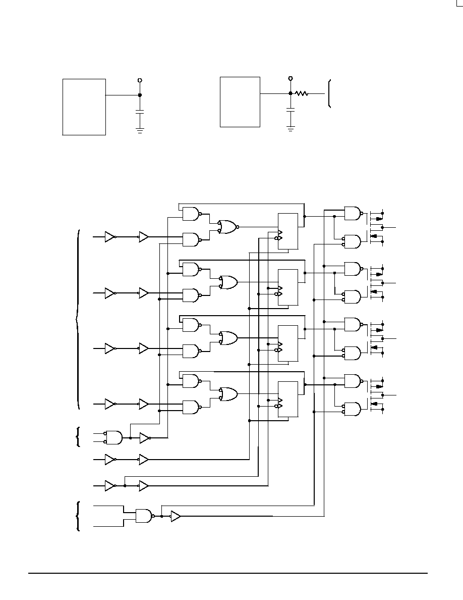
LOGIC DETAIL
D0
14
D1
13
D2
12
D3
11
9
10
DE1
DE2
15
RESET
CLOCK
7
OE1
OE2
1
2
DATA≠
ENABLES
OUTPUT
ENABLES
DATA
INPUTS
C
C
R
Q
VCC
3
Q0
D
C
C
R
Q
D
C
C
R
Q
D
C
C
R
Q
D
VCC
4
Q1
VCC
5
Q2
VCC
6
Q3