 | –≠–ª–µ–∫—Ç—Ä–æ–Ω–Ω—ã–π –∫–æ–º–ø–æ–Ω–µ–Ω—Ç: 74ACT139 | –°–∫–∞—á–∞—Ç—å:  PDF PDF  ZIP ZIP |
5-1
FACT DATA
Dual 1 of 4 Decoder/Demultiplexer
The MC74AC139/74ACT139 is a high-speed, dual 1-of-4 decoder/demultiplexer.
The device has two independent decoders, each accepting two inputs and providing
four mutually-exclusive active-LOW outputs. Each decoder has an active-LOW
Enable input which can be used as a data input for a 4-output demultiplexer. Each
half of the MC74AC139/74ACT139 can be used as a function generator providing
four minterms of two variables.
∑
Multifunction Capability
∑
Two Completely Independent 1-of-4 Decoders
∑
Active LOW Mutually Exclusive Outputs
∑
Outputs Source/Sink 24 mA
∑
ACT139 Has TTL Compatible Inputs
15
16
14
13
12
11
10
2
1
3
4
5
6
7
VCC
9
8
Eb
A0b
A1b
Ea
GND
O0b
O1b
O2b
O3b
A0a
A1a
O0a
O1a
O2a
O3a
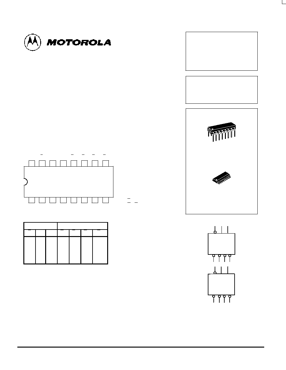
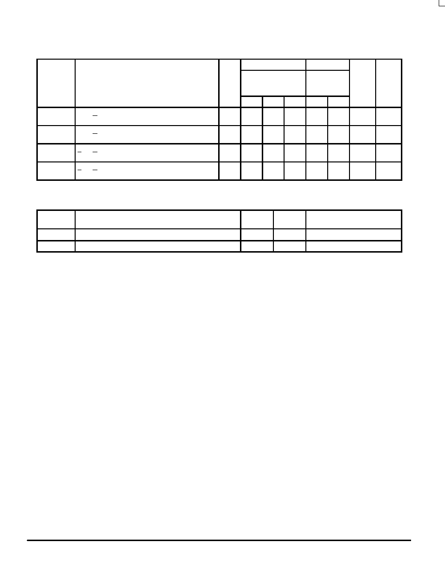
PIN NAMES
A0, A1
Address Inputs
E
Enable Inputs
O0≠O3
Outputs
TRUTH TABLE
Inputs
Outputs
E
A0
A1
O0
O1
O2
O3
H
X
X
H
H
H
H
L
L
L
L
H
H
H
L
H
L
H
L
H
H
L
L
H
H
H
L
H
L
H
H
H
H
H
L
H = HIGH Voltage Level
L = LOW Voltage Level
X = Immaterial
MC74AC139
MC74ACT139
DUAL 1-OF-4
DECODER/DEMULTIPLEXER
N SUFFIX
CASE 648-08
PLASTIC
D SUFFIX
CASE 751B-05
PLASTIC
E A0 A1
O0 O1 O2 O3
DECODER a
LOGIC SYMBOL
E A0 A1
O0 O1 O2 O3
DECODER b
MC74AC139 MC74ACT139
5-2
FACT DATA
Ea
A0a
A1a
Eb
A0b A1b
00a
01a
02a
03a
00b
01b
02b
03b
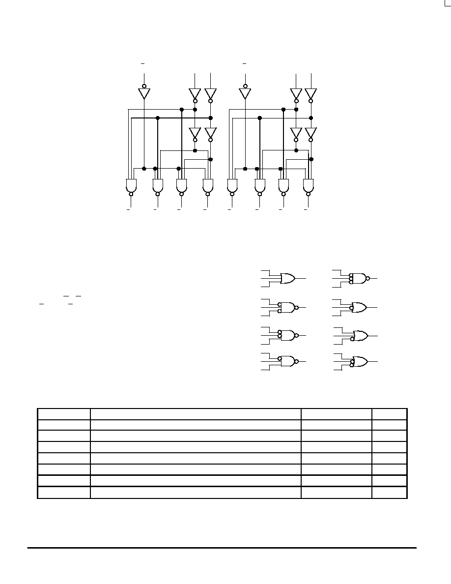
Please note that this diagram is provided only for the understanding of logic
operations and should not be used to estimate propagation delays.
LOGIC DIAGRAM
FUNCTIONAL DESCRIPTION
The MC74AC139/74ACT139 is a high-speed dual 1-of-4
decoder/demultiplexer. The device has two independent
decoders, each of which accepts two binary weighted inputs
(A0≠A1) and provides four mutually exclusive active-LOW
outputs (O0≠O3). Each decoder has an active-LOW enable
(E). When E is HIGH all outputs are forced HIGH. The enable
can be used as the data input for a 4-output demultiplexer
application. Each half of the MC74AC139/74ACT139
generates all four minterms of two variables. These four
minterms are useful in some applications, replacing multiple
gate functions as shown in Figure a, and thereby reducing the
number of packages required in a logic network.
E
A0
A1
E
A0
A1
E
A0
A1
E
A0
A1
E
A0
A1
E
A0
A1
E
A0
A1
E
A0
A1
O0
O0
O1
O1
O2
O2
O3
O3
Figure a: Gate Functions (each half)
MAXIMUM RATINGS*
Symbol
Parameter
Value
Unit
VCC
DC Supply Voltage (Referenced to GND)
≠0.5 to +7.0
V
Vin
DC Input Voltage (Referenced to GND)
≠0.5 to VCC +0.5
V
Vout
DC Output Voltage (Referenced to GND)
≠0.5 to VCC +0.5
V
Iin
DC Input Current, per Pin
±
20
mA
Iout
DC Output Sink/Source Current, per Pin
±
50
mA
ICC
DC VCC or GND Current per Output Pin
±
50
mA
Tstg
Storage Temperature
≠65 to +150
∞
C
* Maximum Ratings are those values beyond which damage to the device may occur. Functional operation should be restricted to the Recommended
Operating Conditions.
MC74AC139 MC74ACT139
5-3
FACT DATA
RECOMMENDED OPERATING CONDITIONS
Symbol
Parameter
Min
Typ
Max
Unit
VCC
Supply Voltage
AC
2.0
5.0
6.0
V
VCC
Supply Voltage
ACT
4.5
5.0
5.5
V
Vin, Vout
DC Input Voltage, Output Voltage (Ref. to GND)
0
VCC
V
tr, tf
Input Rise and Fall Time (Note 1)
AC Devices except Schmitt Inputs
VCC @ 3.0 V
150
tr, tf
Input Rise and Fall Time (Note 1)
AC Devices except Schmitt Inputs
VCC @ 4.5 V
40
ns/V
r, tf
AC Devices except Schmitt Inputs
VCC @ 5.5 V
25
tr, tf
Input Rise and Fall Time (Note 2)
ACT Devices except Schmitt Inputs
VCC @ 4.5 V
10
ns/V
tr, tf
Input Rise and Fall Time (Note 2)
ACT Devices except Schmitt Inputs
VCC @ 5.5 V
8.0
ns/V
TJ
Junction Temperature (PDIP)
140
∞
C
TA
Operating Ambient Temperature Range
≠40
25
85
∞
C
IOH
Output Current -- High
≠24
mA
IOL
Output Current -- Low
24
mA
1. Vin from 30% to 70% VCC; see individual Data Sheets for devices that differ from the typical input rise and fall times.
2. Vin from 0.8 V to 2.0 V; see individual Data Sheets for devices that differ from the typical input rise and fall times.
DC CHARACTERISTICS
Symbol
Parameter
VCC
(V)
74AC
74AC
Unit
Conditions
Symbol
Parameter
VCC
(V)
TA = +25
∞
C
TA =
≠40
∞
C to +85
∞
C
Unit
Conditions
Typ
Guaranteed Limits
VIH
Minimum High Level
Input Voltage
3.0
1.5
2.1
2.1
VOUT = 0.1 V
Input Voltage
4.5
2.25
3.15
3.15
V
or VCC ≠ 0.1 V
5.5
2.75
3.85
3.85
VIL
Maximum Low Level
Input Voltage
3.0
1.5
0.9
0.9
VOUT = 0.1 V
Input Voltage
4.5
2.25
1.35
1.35
V
or VCC ≠ 0.1 V
5.5
2.75
1.65
1.65
VOH
Minimum High Level
Output Voltage
3.0
2.99
2.9
2.9
IOUT = ≠50
µ
A
Output Voltage
4.5
4.49
4.4
4.4
V
5.5
5.49
5.4
5.4
V
*VIN = VIL or VIH
3.0
2.56
2.46
V
≠12 mA
4.5
3.86
3.76
V
IOH
≠24 mA
5.5
4.86
4.76
≠24 mA
VOL
Maximum Low Level
Output Voltage
3.0
0.002
0.1
0.1
IOUT = 50
µ
A
Output Voltage
4.5
0.001
0.1
0.1
V
5.5
0.001
0.1
0.1
V
*VIN = VIL or VIH
3.0
0.36
0.44
V
12 mA
4.5
0.36
0.44
V
IOL
24 mA
5.5
0.36
0.44
24 mA
IIN
Maximum Input
Leakage Current
5.5
±
0.1
±
1.0
µ
A
VI = VCC, GND
Leakage Current
5.5
±
0.1
±
1.0
µ
A
VI = VCC, GND
IOLD
Minimum Dynamic
Output Current
5.5
75
mA
VOLD = 1.65 V Max
IOHD
Output Current
5.5
≠75
mA
VOHD = 3.85 V Min
ICC
Maximum Quiescent
Supply Current
5.5
8.0
80
µ
A
VIN = VCC or GND
Supply Current
5.5
8.0
80
µ
A
VIN = VCC or GND
* All outputs loaded; thresholds on input associated with output under test.
Maximum test duration 2.0 ms, one output loaded at a time.
Note: IIN and ICC @ 3.0 V are guaranteed to be less than or equal to the respective limit @ 5.5 V VCC.
MC74AC139 MC74ACT139
5-4
FACT DATA
AC CHARACTERISTICS (For Figures and Waveforms -- See Section 3)
Symbol
Parameter
VCC*
(V)
74AC
74AC
Unit
Fig.
No.
Symbol
Parameter
VCC*
(V)
TA = +25
∞
C
CL = 50 pF
TA = ≠40
∞
C
to +85
∞
C
CL = 50 pF
Unit
Fig.
No.
Min
Typ
Max
Min
Max
tPLH
Propagation Delay
An to On
3.3
4.0
8.0
11.5
3.5
13
ns
3-6
tPLH
An to On
5.0
3.0
6.5
8.5
2.5
9.5
ns
3-6
tPHL
Propagation Delay
An to On
3.3
3.0
7.0
10
2.5
11
ns
3-6
tPHL
An to On
5.0
2.5
5.5
7.5
2.0
8.5
ns
3-6
tPLH
Propagation Delay
En to On
3.3
4.5
9.5
12
3.5
13
ns
3-6
tPLH
En to On
5.0
3.5
7.0
8.5
3.0
10
ns
3-6
tPHL
Propagation Delay
En to On
3.3
4.0
8.0
10
3.0
11
ns
3-6
tPHL
En to On
5.0
2.5
6.0
7.5
2.5
8.5
ns
3-6
* Voltage Range 3.3 V is 3.3 V
±
0.3 V.
Voltage Range 5.0 V is 5.0 V
±
0.5 V.
DC CHARACTERISTICS
Symbol
Parameter
VCC
(V)
74ACT
74ACT
Unit
Conditions
Symbol
Parameter
VCC
(V)
TA = +25
∞
C
TA =
≠40
∞
C to +85
∞
C
Unit
Conditions
Typ
Guaranteed Limits
VIH
Minimum High Level
Input Voltage
4.5
1.5
2.0
2.0
V
VOUT = 0.1 V
Input Voltage
5.5
1.5
2.0
2.0
V
or VCC ≠ 0.1 V
VIL
Maximum Low Level
Input Voltage
4.5
1.5
0.8
0.8
V
VOUT = 0.1 V
Input Voltage
5.5
1.5
0.8
0.8
V
or VCC ≠ 0.1 V
VOH
Minimum High Level
Output Voltage
4.5
4.49
4.4
4.4
V
IOUT = ≠50
µ
A
Output Voltage
5.5
5.49
5.4
5.4
V
*VIN = VIL or VIH
4.5
3.86
3.76
V
IOH
≠24 mA
5.5
4.86
4.76
IOH
≠24 mA
VOL
Maximum Low Level
Output Voltage
4.5
0.001
0.1
0.1
V
IOUT = 50
µ
A
Output Voltage
5.5
0.001
0.1
0.1
V
*VIN = VIL or VIH
4.5
0.36
0.44
V
IOL
24 mA
5.5
0.36
0.44
IOL
24 mA
IIN
Maximum Input
Leakage Current
5.5
±
0.1
±
1.0
µ
A
VI = VCC, GND
Leakage Current
5.5
±
0.1
±
1.0
µ
A
VI = VCC, GND
ICCT
Additional Max. ICC/Input
5.5
0.6
1.5
mA
VI = VCC ≠ 2.1 V
IOLD
Minimum Dynamic
Output Current
5.5
75
mA
VOLD = 1.65 V Max
IOHD
Output Current
5.5
≠75
mA
VOHD = 3.85 V Min
ICC
Maximum Quiescent
Supply Current
5.5
8.0
80
µ
A
VIN = VCC or GND
Supply Current
5.5
8.0
80
µ
A
VIN = VCC or GND
* All outputs loaded; thresholds on input associated with output under test.
Maximum test duration 2.0 ms, one output loaded at a time.
MC74AC139 MC74ACT139
5-5
FACT DATA
AC CHARACTERISTICS (For Figures and Waveforms -- See Section 3)
Symbol
Parameter
VCC*
(V)
74ACT
74ACT
Unit
Fig.
No.
Symbol
Parameter
VCC*
(V)
TA = +25
∞
C
CL = 50 pF
TA = ≠40
∞
C
to +85
∞
C
CL = 50 pF
Unit
Fig.
No.
Min
Typ
Max
Min
Max
tPLH
Propagation Delay
An to On
5.0
1.5
6.0
8.5
1.5
9.5
ns
3-6
tPLH
An to On
5.0
1.5
6.0
8.5
1.5
9.5
ns
3-6
tPHL
Propagation Delay
An to On
5.0
1.5
6.0
9.5
1.5
10.5
ns
3-6
tPHL
An to On
5.0
1.5
6.0
9.5
1.5
10.5
ns
3-6
tPLH
Propagation Delay
En to On
5.0
2.5
7.0
10.0
2.0
11.0
ns
3-6
tPLH
En to On
5.0
2.5
7.0
10.0
2.0
11.0
ns
3-6
tPHL
Propagation Delay
En to On
5.0
2.0
7.0
9.5
1.5
10.5
ns
3-6
tPHL
En to On
5.0
2.0
7.0
9.5
1.5
10.5
ns
3-6
* Voltage Range 5.0 V is 5.0 V
±
0.5 V.
CAPACITANCE
Symbol
Parameter
Value
Typ
Unit
Test Conditions
CIN
Input Capacitance
4.5
pF
VCC = 5.0 V
CPD
Power Dissipation Capacitance
40
pF
VCC = 5.0 V
MC74AC139 MC74ACT139
5-6
FACT DATA
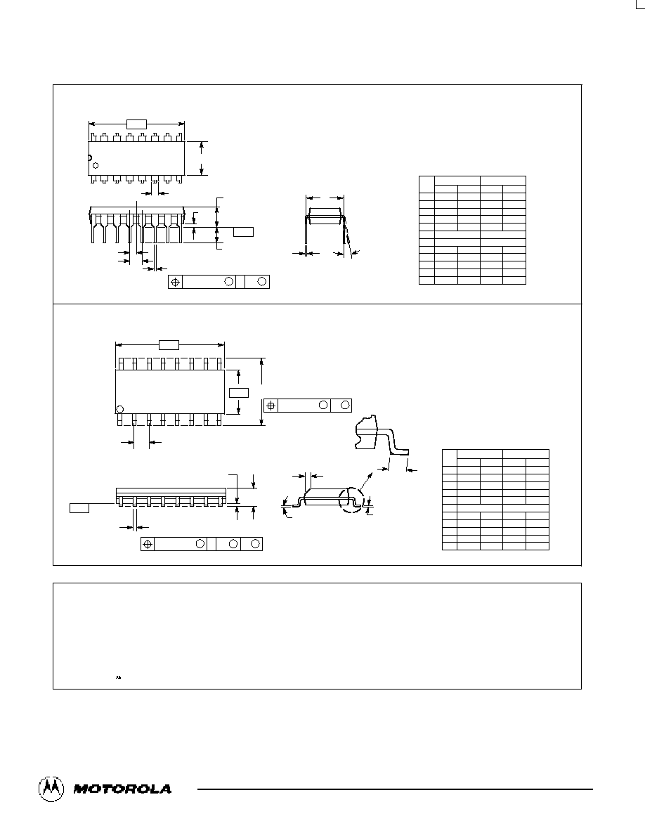
OUTLINE DIMENSIONS
N SUFFIX
PLASTIC DIP PACKAGE
CASE 648≠08
ISSUE R
D SUFFIX
PLASTIC SOIC PACKAGE
CASE 751B≠05
ISSUE J
NOTES:
1. DIMENSIONING AND TOLERANCING PER
ANSI Y14.5M, 1982.
2. CONTROLLING DIMENSION: MILLIMETER.
3. DIMENSIONS A AND B DO NOT INCLUDE
MOLD PROTRUSION.
4. MAXIMUM MOLD PROTRUSION 0.15 (0.006)
PER SIDE.
5. DIMENSION D DOES NOT INCLUDE DAMBAR
PROTRUSION. ALLOWABLE DAMBAR
PROTRUSION SHALL BE 0.127 (0.005) TOTAL
IN EXCESS OF THE D DIMENSION AT
MAXIMUM MATERIAL CONDITION.
1
8
16
9
SEATING
PLANE
F
J
M
R
X 45
_
G
8 PL
P
≠B≠
≠A≠
M
0.25 (0.010)
B
S
≠T≠
D
K
C
16 PL
S
B
M
0.25 (0.010)
A
S
T
DIM
MIN
MAX
MIN
MAX
INCHES
MILLIMETERS
A
9.80
10.00
0.386
0.393
B
3.80
4.00
0.150
0.157
C
1.35
1.75
0.054
0.068
D
0.35
0.49
0.014
0.019
F
0.40
1.25
0.016
0.049
G
1.27 BSC
0.050 BSC
J
0.19
0.25
0.008
0.009
K
0.10
0.25
0.004
0.009
M
0
7
0
7
P
5.80
6.20
0.229
0.244
R
0.25
0.50
0.010
0.019
_
_
_
_
NOTES:
1. DIMENSIONING AND TOLERANCING PER ANSI
Y14.5M, 1982.
2. CONTROLLING DIMENSION: INCH.
3. DIMENSION L TO CENTER OF LEADS WHEN
FORMED PARALLEL.
4. DIMENSION B DOES NOT INCLUDE MOLD FLASH.
5. ROUNDED CORNERS OPTIONAL.
≠A≠
B
F
C
S
H
G
D
J
L
M
16 PL
SEATING
1
8
9
16
K
PLANE
≠T≠
M
A
M
0.25 (0.010)
T
DIM
MIN
MAX
MIN
MAX
MILLIMETERS
INCHES
A
0.740
0.770
18.80
19.55
B
0.250
0.270
6.35
6.85
C
0.145
0.175
3.69
4.44
D
0.015
0.021
0.39
0.53
F
0.040
0.70
1.02
1.77
G
0.100 BSC
2.54 BSC
H
0.050 BSC
1.27 BSC
J
0.008
0.015
0.21
0.38
K
0.110
0.130
2.80
3.30
L
0.295
0.305
7.50
7.74
M
0
10
0
10
S
0.020
0.040
0.51
1.01
_
_
_
_
How to reach us:
USA/EUROPE: Motorola Literature Distribution;
JAPAN: Nippon Motorola Ltd.; Tatsumi≠SPD≠JLDC, Toshikatsu Otsuki,
P.O. Box 20912; Phoenix, Arizona 85036. 1≠800≠441≠2447
6F Seibu≠Butsuryu≠Center, 3≠14≠2 Tatsumi Koto≠Ku, Tokyo 135, Japan. 03≠3521≠8315
MFAX: RMFAX0@email.sps.mot.com ≠TOUCHTONE (602) 244≠6609
HONG KONG: Motorola Semiconductors H.K. Ltd.; 8B Tai Ping Industrial Park,
INTERNET: http://Design≠NET.com
51 Ting Kok Road, Tai Po, N.T., Hong Kong. 852≠26629298
Motorola reserves the right to make changes without further notice to any products herein. Motorola makes no warranty, representation or guarantee regarding
the suitability of its products for any particular purpose, nor does Motorola assume any liability arising out of the application or use of any product or circuit, and
specifically disclaims any and all liability, including without limitation consequential or incidental damages. "Typical" parameters can and do vary in different
applications. All operating parameters, including "Typicals" must be validated for each customer application by customer's technical experts. Motorola does
not convey any license under its patent rights nor the rights of others. Motorola products are not designed, intended, or authorized for use as components in
systems intended for surgical implant into the body, or other applications intended to support or sustain life, or for any other application in which the failure of
the Motorola product could create a situation where personal injury or death may occur. Should Buyer purchase or use Motorola products for any such
unintended or unauthorized application, Buyer shall indemnify and hold Motorola and its officers, employees, subsidiaries, affiliates, and distributors harmless
against all claims, costs, damages, and expenses, and reasonable attorney fees arising out of, directly or indirectly, any claim of personal injury or death
associated with such unintended or unauthorized use, even if such claim alleges that Motorola was negligent regarding the design or manufacture of the part.
Motorola and
are registered trademarks of Motorola, Inc. Motorola, Inc. is an Equal Opportunity/Affirmative Action Employer.
MC74AC139/D
*MC74AC139/D*