 | –≠–ª–µ–∫—Ç—Ä–æ–Ω–Ω—ã–π –∫–æ–º–ø–æ–Ω–µ–Ω—Ç: 74HC4538A | –°–∫–∞—á–∞—Ç—å:  PDF PDF  ZIP ZIP |
MOTOROLA
SEMICONDUCTOR TECHNICAL DATA
3≠1
REV 6
©
Motorola, Inc. 1995
10/95
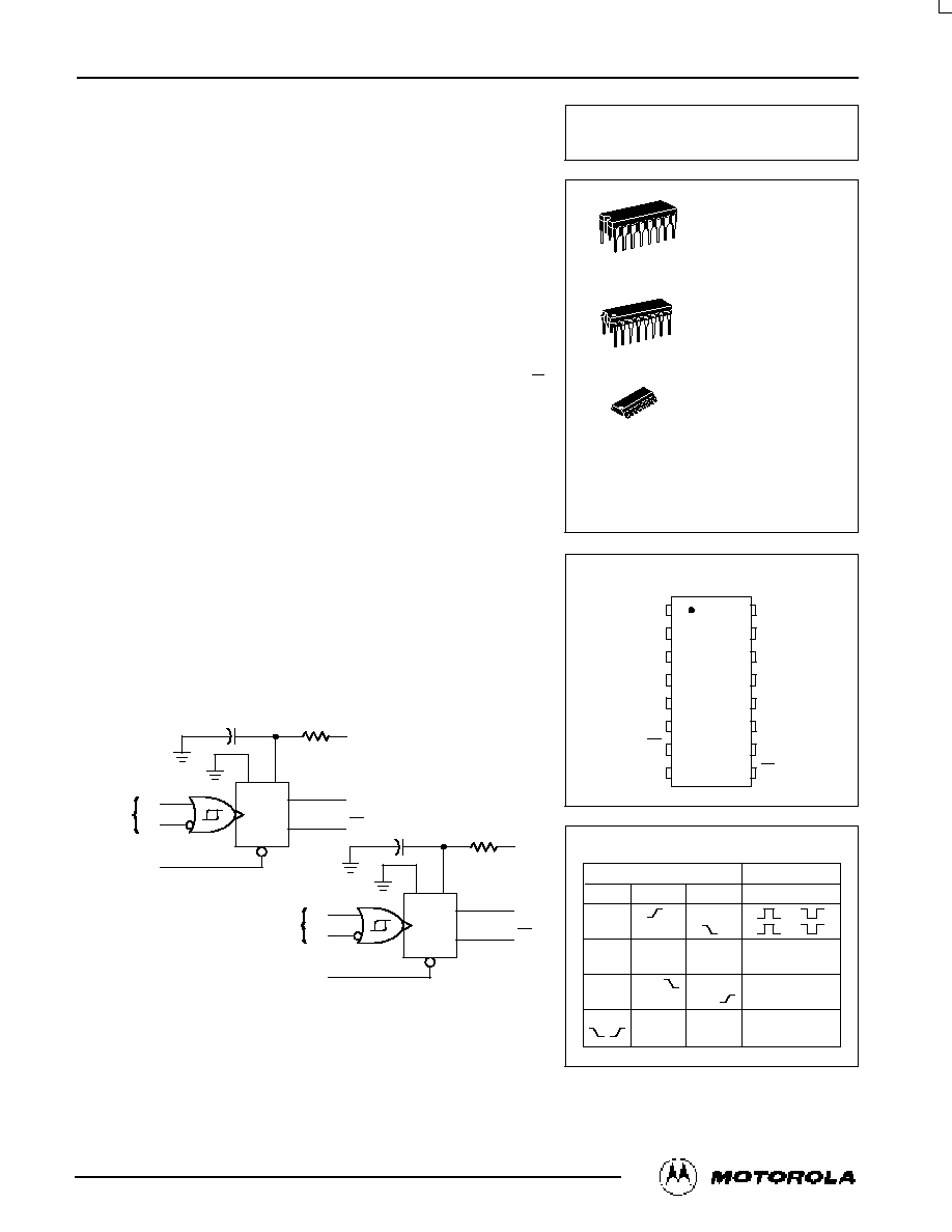
Dual Precision
Monostable Multivibrator
(Retriggerable, Resettable)
The MC54/74HC4538A is identical in pinout to the MC14538B. The device
inputs are compatible with standard CMOS outputs; with pullup resistors,
they are compatible with LSTTL outputs.
This dual monostable multivibrator may be triggered by either the positive
or the negative edge of an input pulse, and produces a precision output
pulse over a wide range of pulse widths. Because the device has conditioned
trigger inputs, there are no trigger≠input rise and fall time restrictions. The
output pulse width is determined by the external timing components, Rx and
Cx. The device has a reset function which forces the Q output low and the Q
output high, regardless of the state of the output pulse circuitry.
∑
Unlimited Rise and Fall Times Allowed on the Trigger Inputs
∑
Output Pulse is Independent of the Trigger Pulse Width
∑ ±
10% Guaranteed Pulse Width Variation from Part to Part (Using the
Same Test Jig)
∑
Output Drive Capability: 10 LSTTL Loads
∑
Outputs Directly Interface to CMOS, NMOS and TTL
∑
Operating Voltage Range: 3.0 to 6.0 V
∑
Low Input Current: 1.0
µ
A
∑
High Noise Immunity Characteristic of CMOS Devices
∑
In Compliance with the Requirements Defined by JEDEC Standard
No. 7A
∑
Chip Complexity: 145 FETs or 36 Equivalent Gates
LOGIC DIAGRAM
PIN 16 = VCC
PIN 8 = GND
RX AND CX ARE EXTERNAL COMPONENTS
PIN 1 AND PIN 15 MUST BE HARD WIRED TO GND
CX1
RX1
VCC
Q1
RESET 1
B1
A1
TRIGGER
INPUTS
Q1
1
2
4
5
3
6
7
CX2
RX2
VCC
Q2
RESET 2
B2
A2
TRIGGER
INPUTS
Q2
15
14
12
11
13
10
9
MC54/74HC4538A
PIN ASSIGNMENT
13
14
15
16
9
10
11
12
5
4
3
2
1
8
7
6
A2
RESET 2
CX2/RX2
GND
VCC
Q2
Q2
B2
A1
RESET 1
CX1/RX1
GND
GND
Q1
Q1
B1
FUNCTION TABLE
Inputs
Outputs
Reset
A
B
Q
Q
H
H
H
L
H
X
L
Not Triggered
H
H
X
Not Triggered
H
L,H,
H
Not Triggered
H
L
L,H,
Not Triggered
L
X
X
L
H
X
X
Not Triggered
D SUFFIX
SOIC PACKAGE
CASE 751B≠05
N SUFFIX
PLASTIC PACKAGE
CASE 648≠08
ORDERING INFORMATION
MC54HCXXXXAJ
MC74HCXXXXAN
MC74HCXXXXAD
Ceramic
Plastic
SOIC
1
16
1
16
J SUFFIX
CERAMIC PACKAGE
CASE 620≠10
1
16
MC54/74HC4538A
MOTOROLA
High≠Speed CMOS Logic Data
DL129 -- Rev 6
3≠2
ŒŒŒŒŒŒŒŒŒŒŒŒŒŒŒŒŒŒŒŒŒŒŒ
ŒŒŒŒŒŒŒŒŒŒŒŒŒŒŒŒŒŒŒŒŒŒŒ
ŒŒŒŒŒŒŒŒŒŒŒŒŒŒŒŒŒŒŒŒŒŒŒ
ŒŒŒŒŒŒŒŒŒŒŒŒŒŒŒŒŒŒŒŒŒŒŒ
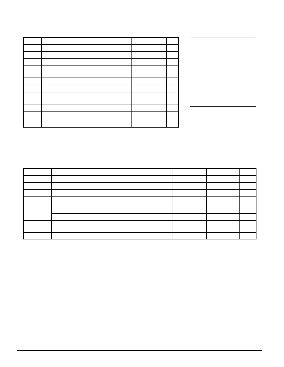
MAXIMUM RATINGS*
ŒŒŒ
ŒŒŒ
ŒŒŒ
ŒŒŒ
Symbol
ŒŒŒŒŒŒŒŒŒŒŒŒŒŒ
ŒŒŒŒŒŒŒŒŒŒŒŒŒŒ
ŒŒŒŒŒŒŒŒŒŒŒŒŒŒ
ŒŒŒŒŒŒŒŒŒŒŒŒŒŒ
Parameter
ŒŒŒŒŒŒ
ŒŒŒŒŒŒ
ŒŒŒŒŒŒ
ŒŒŒŒŒŒ
Value
ŒŒŒ
ŒŒŒ
ŒŒŒ
ŒŒŒ
Unit
ŒŒŒ
ŒŒŒ
ŒŒŒ
ŒŒŒ
VCC
ŒŒŒŒŒŒŒŒŒŒŒŒŒŒ
ŒŒŒŒŒŒŒŒŒŒŒŒŒŒ
ŒŒŒŒŒŒŒŒŒŒŒŒŒŒ
ŒŒŒŒŒŒŒŒŒŒŒŒŒŒ
DC Supply Voltage (Referenced to GND)
ŒŒŒŒŒŒ
ŒŒŒŒŒŒ
ŒŒŒŒŒŒ
ŒŒŒŒŒŒ
≠ 0.5 to + 7.0
ŒŒŒ
ŒŒŒ
ŒŒŒ
ŒŒŒ
V
ŒŒŒ
ŒŒŒ
ŒŒŒ
ŒŒŒ
Vin
ŒŒŒŒŒŒŒŒŒŒŒŒŒŒ
ŒŒŒŒŒŒŒŒŒŒŒŒŒŒ
ŒŒŒŒŒŒŒŒŒŒŒŒŒŒ
ŒŒŒŒŒŒŒŒŒŒŒŒŒŒ
DC Input Voltage (Referenced to GND)
ŒŒŒŒŒŒ
ŒŒŒŒŒŒ
ŒŒŒŒŒŒ
ŒŒŒŒŒŒ
≠ 1.5 to VCC + 1.5
ŒŒŒ
ŒŒŒ
ŒŒŒ
ŒŒŒ
V
ŒŒŒ
ŒŒŒ
ŒŒŒ
ŒŒŒ
Vout
ŒŒŒŒŒŒŒŒŒŒŒŒŒŒ
ŒŒŒŒŒŒŒŒŒŒŒŒŒŒ
ŒŒŒŒŒŒŒŒŒŒŒŒŒŒ
ŒŒŒŒŒŒŒŒŒŒŒŒŒŒ
DC Output Voltage (Referenced to GND)
ŒŒŒŒŒŒ
ŒŒŒŒŒŒ
ŒŒŒŒŒŒ
ŒŒŒŒŒŒ
≠ 0.5 to VCC + 0.5
ŒŒŒ
ŒŒŒ
ŒŒŒ
ŒŒŒ
ŒŒŒ
ŒŒŒ
ŒŒŒ
ŒŒŒ
ŒŒŒ
Iin
ŒŒŒŒŒŒŒŒŒŒŒŒŒŒ
ŒŒŒŒŒŒŒŒŒŒŒŒŒŒ
ŒŒŒŒŒŒŒŒŒŒŒŒŒŒ
ŒŒŒŒŒŒŒŒŒŒŒŒŒŒ
ŒŒŒŒŒŒŒŒŒŒŒŒŒŒ
DC Input Current, per Pin
A, B, Reset
Cx, Rx
ŒŒŒŒŒŒ
ŒŒŒŒŒŒ
ŒŒŒŒŒŒ
ŒŒŒŒŒŒ
ŒŒŒŒŒŒ
±
20
±
30
ŒŒŒ
ŒŒŒ
ŒŒŒ
ŒŒŒ
ŒŒŒ
mA
ŒŒŒ
ŒŒŒ
ŒŒŒ
ŒŒŒ
Iout
ŒŒŒŒŒŒŒŒŒŒŒŒŒŒ
ŒŒŒŒŒŒŒŒŒŒŒŒŒŒ
ŒŒŒŒŒŒŒŒŒŒŒŒŒŒ
ŒŒŒŒŒŒŒŒŒŒŒŒŒŒ
DC Output Current, per Pin
ŒŒŒŒŒŒ
ŒŒŒŒŒŒ
ŒŒŒŒŒŒ
ŒŒŒŒŒŒ
±
25
ŒŒŒ
ŒŒŒ
ŒŒŒ
ŒŒŒ
mA
ŒŒŒ
ŒŒŒ
ŒŒŒ
ŒŒŒ
ICC
ŒŒŒŒŒŒŒŒŒŒŒŒŒŒ
ŒŒŒŒŒŒŒŒŒŒŒŒŒŒ
ŒŒŒŒŒŒŒŒŒŒŒŒŒŒ
ŒŒŒŒŒŒŒŒŒŒŒŒŒŒ
DC Supply Current, VCC and GND Pins
ŒŒŒŒŒŒ
ŒŒŒŒŒŒ
ŒŒŒŒŒŒ
ŒŒŒŒŒŒ
±
50
ŒŒŒ
ŒŒŒ
ŒŒŒ
ŒŒŒ
mA
ŒŒŒ
ŒŒŒ
ŒŒŒ
ŒŒŒ
ŒŒŒ
PD
ŒŒŒŒŒŒŒŒŒŒŒŒŒŒ
ŒŒŒŒŒŒŒŒŒŒŒŒŒŒ
ŒŒŒŒŒŒŒŒŒŒŒŒŒŒ
ŒŒŒŒŒŒŒŒŒŒŒŒŒŒ
ŒŒŒŒŒŒŒŒŒŒŒŒŒŒ
Power Dissipation in Still Air, Plastic or Ceramic DIP
SOIC Package
ŒŒŒŒŒŒ
ŒŒŒŒŒŒ
ŒŒŒŒŒŒ
ŒŒŒŒŒŒ
ŒŒŒŒŒŒ
750
500
ŒŒŒ
ŒŒŒ
ŒŒŒ
ŒŒŒ
ŒŒŒ
mW
ŒŒŒ
ŒŒŒ
ŒŒŒ
ŒŒŒ
Tstg
ŒŒŒŒŒŒŒŒŒŒŒŒŒŒ
ŒŒŒŒŒŒŒŒŒŒŒŒŒŒ
ŒŒŒŒŒŒŒŒŒŒŒŒŒŒ
ŒŒŒŒŒŒŒŒŒŒŒŒŒŒ
Storage Temperature
ŒŒŒŒŒŒ
ŒŒŒŒŒŒ
ŒŒŒŒŒŒ
ŒŒŒŒŒŒ
≠ 65 to + 150
ŒŒŒ
ŒŒŒ
ŒŒŒ
ŒŒŒ
_
C
ŒŒŒ
ŒŒŒ
ŒŒŒ
ŒŒŒ
ŒŒŒ
TL
ŒŒŒŒŒŒŒŒŒŒŒŒŒŒ
ŒŒŒŒŒŒŒŒŒŒŒŒŒŒ
ŒŒŒŒŒŒŒŒŒŒŒŒŒŒ
ŒŒŒŒŒŒŒŒŒŒŒŒŒŒ
ŒŒŒŒŒŒŒŒŒŒŒŒŒŒ
Lead Temperature, 1 mm from Case for 10 Seconds
(Plastic DIP or SOIC Package)
(Ceramic DIP)
ŒŒŒŒŒŒ
ŒŒŒŒŒŒ
ŒŒŒŒŒŒ
ŒŒŒŒŒŒ
ŒŒŒŒŒŒ
260
300
ŒŒŒ
ŒŒŒ
ŒŒŒ
ŒŒŒ
ŒŒŒ
_
C
* Maximum Ratings are those values beyond which damage to the device may occur.
Functional operation should be restricted to the Recommended Operating Conditions.
Derating -- Plastic DIP: ≠ 10 mW/
_
C from 65
_
to 125
_
C
Ceramic DIP: ≠ 10 mW/
_
C from 100
_
to 125
_
C
SOIC Package: ≠ 7 mW/
_
C from 65
_
to 125
_
C
For high frequency or heavy load considerations, see Chapter 2 of the Motorola High≠Speed CMOS Data Book (DL129/D).
RECOMMENDED OPERATING CONDITIONS
ŒŒŒŒŒ
ŒŒŒŒŒ
ŒŒŒŒŒ
ŒŒŒŒŒ
Symbol
ŒŒŒŒŒŒŒŒŒŒŒŒŒŒŒŒŒŒ
ŒŒŒŒŒŒŒŒŒŒŒŒŒŒŒŒŒŒ
ŒŒŒŒŒŒŒŒŒŒŒŒŒŒŒŒŒŒ
ŒŒŒŒŒŒŒŒŒŒŒŒŒŒŒŒŒŒ
Parameter
ŒŒŒŒŒ
ŒŒŒŒŒ
ŒŒŒŒŒ
ŒŒŒŒŒ
Min
ŒŒŒŒŒŒ
ŒŒŒŒŒŒ
ŒŒŒŒŒŒ
ŒŒŒŒŒŒ
Max
ŒŒŒ
ŒŒŒ
ŒŒŒ
ŒŒŒ
Unit
ŒŒŒŒŒ
ŒŒŒŒŒ
ŒŒŒŒŒ
ŒŒŒŒŒ
VCC
ŒŒŒŒŒŒŒŒŒŒŒŒŒŒŒŒŒŒ
ŒŒŒŒŒŒŒŒŒŒŒŒŒŒŒŒŒŒ
ŒŒŒŒŒŒŒŒŒŒŒŒŒŒŒŒŒŒ
ŒŒŒŒŒŒŒŒŒŒŒŒŒŒŒŒŒŒ
DC Supply Voltage (Referenced to GND)
ŒŒŒŒŒ
ŒŒŒŒŒ
ŒŒŒŒŒ
ŒŒŒŒŒ
3.0**
ŒŒŒŒŒŒ
ŒŒŒŒŒŒ
ŒŒŒŒŒŒ
ŒŒŒŒŒŒ
6.0
ŒŒŒ
ŒŒŒ
ŒŒŒ
ŒŒŒ
V
ŒŒŒŒŒ
ŒŒŒŒŒ
ŒŒŒŒŒ
ŒŒŒŒŒ
Vin, Vout
ŒŒŒŒŒŒŒŒŒŒŒŒŒŒŒŒŒŒ
ŒŒŒŒŒŒŒŒŒŒŒŒŒŒŒŒŒŒ
ŒŒŒŒŒŒŒŒŒŒŒŒŒŒŒŒŒŒ
ŒŒŒŒŒŒŒŒŒŒŒŒŒŒŒŒŒŒ
DC Input Voltage, Output Voltage (Referenced to GND)
ŒŒŒŒŒ
ŒŒŒŒŒ
ŒŒŒŒŒ
ŒŒŒŒŒ
0
ŒŒŒŒŒŒ
ŒŒŒŒŒŒ
ŒŒŒŒŒŒ
ŒŒŒŒŒŒ
VCC
ŒŒŒ
ŒŒŒ
ŒŒŒ
ŒŒŒ
V
ŒŒŒŒŒ
ŒŒŒŒŒ
ŒŒŒŒŒ
ŒŒŒŒŒ
TA
ŒŒŒŒŒŒŒŒŒŒŒŒŒŒŒŒŒŒ
ŒŒŒŒŒŒŒŒŒŒŒŒŒŒŒŒŒŒ
ŒŒŒŒŒŒŒŒŒŒŒŒŒŒŒŒŒŒ
ŒŒŒŒŒŒŒŒŒŒŒŒŒŒŒŒŒŒ
Operating Temperature, All Package Types
ŒŒŒŒŒ
ŒŒŒŒŒ
ŒŒŒŒŒ
ŒŒŒŒŒ
≠ 55
ŒŒŒŒŒŒ
ŒŒŒŒŒŒ
ŒŒŒŒŒŒ
ŒŒŒŒŒŒ
+ 125
ŒŒŒ
ŒŒŒ
ŒŒŒ
ŒŒŒ
_
C
ŒŒŒŒŒ
ŒŒŒŒŒ
ŒŒŒŒŒ
ŒŒŒŒŒ
ŒŒŒŒŒ
tr, tf
ŒŒŒŒŒŒŒŒŒŒŒŒŒŒŒŒŒŒ
ŒŒŒŒŒŒŒŒŒŒŒŒŒŒŒŒŒŒ
ŒŒŒŒŒŒŒŒŒŒŒŒŒŒŒŒŒŒ
ŒŒŒŒŒŒŒŒŒŒŒŒŒŒŒŒŒŒ
ŒŒŒŒŒŒŒŒŒŒŒŒŒŒŒŒŒŒ
Input Rise and Fall Time
VCC = 2.0 V
(Figure 7)
VCC = 4.5 V
VCC = 6.0 V
ŒŒŒŒŒ
ŒŒŒŒŒ
ŒŒŒŒŒ
ŒŒŒŒŒ
ŒŒŒŒŒ
0
0
0
ŒŒŒŒŒŒ
ŒŒŒŒŒŒ
ŒŒŒŒŒŒ
ŒŒŒŒŒŒ
ŒŒŒŒŒŒ
1000
500
400
ŒŒŒ
ŒŒŒ
ŒŒŒ
ŒŒŒ
ŒŒŒ
ns
ŒŒŒŒŒ
ŒŒŒŒŒ
ŒŒŒŒŒ
ŒŒŒŒŒ
ŒŒŒŒŒŒŒŒŒŒŒŒŒŒŒŒŒŒ
ŒŒŒŒŒŒŒŒŒŒŒŒŒŒŒŒŒŒ
ŒŒŒŒŒŒŒŒŒŒŒŒŒŒŒŒŒŒ
ŒŒŒŒŒŒŒŒŒŒŒŒŒŒŒŒŒŒ
A or B (Figure 5)
ŒŒŒŒŒ
ŒŒŒŒŒ
ŒŒŒŒŒ
ŒŒŒŒŒ
--
ŒŒŒŒŒŒ
ŒŒŒŒŒŒ
ŒŒŒŒŒŒ
ŒŒŒŒŒŒ
No Limit
ŒŒŒ
ŒŒŒ
ŒŒŒ
ŒŒŒ
ŒŒŒŒŒ
ŒŒŒŒŒ
ŒŒŒŒŒ
ŒŒŒŒŒ
ŒŒŒŒŒ
Rx
ŒŒŒŒŒŒŒŒŒŒŒŒŒŒŒŒŒŒ
ŒŒŒŒŒŒŒŒŒŒŒŒŒŒŒŒŒŒ
ŒŒŒŒŒŒŒŒŒŒŒŒŒŒŒŒŒŒ
ŒŒŒŒŒŒŒŒŒŒŒŒŒŒŒŒŒŒ
ŒŒŒŒŒŒŒŒŒŒŒŒŒŒŒŒŒŒ
External Timing Resistor
VCC < 4.5 V
VCC
4.5 V
ŒŒŒŒŒ
ŒŒŒŒŒ
ŒŒŒŒŒ
ŒŒŒŒŒ
ŒŒŒŒŒ
1.0
2.0
ŒŒŒŒŒŒ
ŒŒŒŒŒŒ
ŒŒŒŒŒŒ
ŒŒŒŒŒŒ
ŒŒŒŒŒŒ
*
*
ŒŒŒ
ŒŒŒ
ŒŒŒ
ŒŒŒ
ŒŒŒ
k
ŒŒŒŒŒ
ŒŒŒŒŒ
ŒŒŒŒŒ
ŒŒŒŒŒ
Cx
ŒŒŒŒŒŒŒŒŒŒŒŒŒŒŒŒŒŒ
ŒŒŒŒŒŒŒŒŒŒŒŒŒŒŒŒŒŒ
ŒŒŒŒŒŒŒŒŒŒŒŒŒŒŒŒŒŒ
ŒŒŒŒŒŒŒŒŒŒŒŒŒŒŒŒŒŒ
External Timing Capacitor
ŒŒŒŒŒ
ŒŒŒŒŒ
ŒŒŒŒŒ
ŒŒŒŒŒ
0
ŒŒŒŒŒŒ
ŒŒŒŒŒŒ
ŒŒŒŒŒŒ
ŒŒŒŒŒŒ
*
ŒŒŒ
ŒŒŒ
ŒŒŒ
ŒŒŒ
µ
F
* The maximum allowable values of Rx and Cx are a function of the leakage of capacitor Cx, the leakage of the HC4538A, and leakage due to
board layout and surface resistance. For most applications, Cx/Rx should be limited to a maximum value of 10
µ
F/1.0 M
. Values of Cx > 1.0
µ
F
may cause a problem during power down (see Power Down Considerations). Susceptibility to externally induced noise signals may occur for
Rx > 1.0 M
.
** The HC4538A will function at 2.0 V but for optimum pulse width stability, VCC should be above 3.0 V.
NOTE: Information on typical parametric values can be found in Chapter 2 of the Motorola High≠Speed CMOS Data Book (DL129/D).
This device contains protection
circuitry to guard against damage
due to high static voltages or electric
fields. However, precautions must
be taken to avoid applications of any
voltage higher than maximum rated
voltages to this high≠impedance cir-
cuit. For proper operation, Vin and
Vout should be constrained to the
range GND
v
(Vin or Vout)
v
VCC.
Unused inputs must always be
tied to an appropriate logic voltage
level (e.g., either GND or VCC).
Unused outputs must be left open.
MC54/74HC4538A
High≠Speed CMOS Logic Data
DL129 -- Rev 6
3≠3
MOTOROLA
ŒŒŒŒŒŒŒŒŒŒŒŒŒŒŒŒŒŒŒŒŒŒŒŒŒŒŒŒŒŒŒŒŒ
ŒŒŒŒŒŒŒŒŒŒŒŒŒŒŒŒŒŒŒŒŒŒŒŒŒŒŒŒŒŒŒŒŒ
ŒŒŒŒŒŒŒŒŒŒŒŒŒŒŒŒŒŒŒŒŒŒŒŒŒŒŒŒŒŒŒŒŒ
ŒŒŒŒŒŒŒŒŒŒŒŒŒŒŒŒŒŒŒŒŒŒŒŒŒŒŒŒŒŒŒŒŒ
DC CHARACTERISTICS FOR THE MC54/74HC4538A
ŒŒŒ
ŒŒŒ
ŒŒŒ
ŒŒŒ
Symbol
ŒŒŒŒŒŒŒŒ
ŒŒŒŒŒŒŒŒ
ŒŒŒŒŒŒŒŒ
ŒŒŒŒŒŒŒŒ
Parameter
ŒŒŒŒŒŒŒŒŒ
ŒŒŒŒŒŒŒŒŒ
ŒŒŒŒŒŒŒŒŒ
ŒŒŒŒŒŒŒŒŒ
Test Conditions
ŒŒŒ
ŒŒŒ
ŒŒŒ
ŒŒŒ
VCC
Volts
ŒŒŒŒŒŒŒŒŒŒŒŒ
ŒŒŒŒŒŒŒŒŒŒŒŒ
ŒŒŒŒŒŒŒŒŒŒŒŒ
ŒŒŒŒŒŒŒŒŒŒŒŒ
Guaranteed Limits
ŒŒŒ
ŒŒŒ
ŒŒŒ
ŒŒŒ
Unit
ŒŒŒ
ŒŒŒ
ŒŒŒ
ŒŒŒ
ŒŒŒ
Symbol
ŒŒŒŒŒŒŒŒ
ŒŒŒŒŒŒŒŒ
ŒŒŒŒŒŒŒŒ
ŒŒŒŒŒŒŒŒ
ŒŒŒŒŒŒŒŒ
Parameter
ŒŒŒŒŒŒŒŒŒ
ŒŒŒŒŒŒŒŒŒ
ŒŒŒŒŒŒŒŒŒ
ŒŒŒŒŒŒŒŒŒ
ŒŒŒŒŒŒŒŒŒ
Test Conditions
ŒŒŒ
ŒŒŒ
ŒŒŒ
ŒŒŒ
ŒŒŒ
VCC
Volts
ŒŒŒŒŒ
ŒŒŒŒŒ
ŒŒŒŒŒ
ŒŒŒŒŒ
ŒŒŒŒŒ
≠ 55 to
25
_
C
ŒŒŒŒŒ
ŒŒŒŒŒ
ŒŒŒŒŒ
ŒŒŒŒŒ
ŒŒŒŒŒ
v
85
_
C
ŒŒŒŒ
ŒŒŒŒ
ŒŒŒŒ
ŒŒŒŒ
ŒŒŒŒ
v
125
_
C
ŒŒŒ
ŒŒŒ
ŒŒŒ
ŒŒŒ
ŒŒŒ
Unit
ŒŒŒ
ŒŒŒ
ŒŒŒ
ŒŒŒ
Symbol
ŒŒŒŒŒŒŒŒ
ŒŒŒŒŒŒŒŒ
ŒŒŒŒŒŒŒŒ
ŒŒŒŒŒŒŒŒ
Parameter
ŒŒŒŒŒŒŒŒŒ
ŒŒŒŒŒŒŒŒŒ
ŒŒŒŒŒŒŒŒŒ
ŒŒŒŒŒŒŒŒŒ
Test Conditions
ŒŒŒ
ŒŒŒ
ŒŒŒ
ŒŒŒ
VCC
Volts
ŒŒŒ
ŒŒŒ
ŒŒŒ
ŒŒŒ
Min
ŒŒŒ
ŒŒŒ
ŒŒŒ
ŒŒŒ
Max
ŒŒŒ
ŒŒŒ
ŒŒŒ
ŒŒŒ
Min
ŒŒŒ
ŒŒŒ
ŒŒŒ
ŒŒŒ
Max
ŒŒŒ
ŒŒŒ
ŒŒŒ
ŒŒŒ
Min
ŒŒ
ŒŒ
ŒŒ
ŒŒ
Max
ŒŒŒ
ŒŒŒ
ŒŒŒ
ŒŒŒ
Unit
ŒŒŒ
ŒŒŒ
ŒŒŒ
ŒŒŒ
ŒŒŒ
VIH
ŒŒŒŒŒŒŒŒ
ŒŒŒŒŒŒŒŒ
ŒŒŒŒŒŒŒŒ
ŒŒŒŒŒŒŒŒ
ŒŒŒŒŒŒŒŒ
Minimum High≠Level
Input Voltage
ŒŒŒŒŒŒŒŒŒ
ŒŒŒŒŒŒŒŒŒ
ŒŒŒŒŒŒŒŒŒ
ŒŒŒŒŒŒŒŒŒ
ŒŒŒŒŒŒŒŒŒ
Vout = 0.1 V or VCC ≠ 0.1 V
|Iout|
v
20
µ
A
ŒŒŒ
ŒŒŒ
ŒŒŒ
ŒŒŒ
ŒŒŒ
2.0
4.5
6.0
ŒŒŒ
ŒŒŒ
ŒŒŒ
ŒŒŒ
ŒŒŒ
1.5
3.15
4.2
ŒŒŒ
ŒŒŒ
ŒŒŒ
ŒŒŒ
ŒŒŒ
ŒŒŒ
ŒŒŒ
ŒŒŒ
ŒŒŒ
ŒŒŒ
1.5
3.15
4.2
ŒŒŒ
ŒŒŒ
ŒŒŒ
ŒŒŒ
ŒŒŒ
ŒŒŒ
ŒŒŒ
ŒŒŒ
ŒŒŒ
ŒŒŒ
1.5
3.15
4.2
ŒŒ
ŒŒ
ŒŒ
ŒŒ
ŒŒ
ŒŒŒ
ŒŒŒ
ŒŒŒ
ŒŒŒ
ŒŒŒ
V
ŒŒŒ
ŒŒŒ
ŒŒŒ
ŒŒŒ
ŒŒŒ
VIL
ŒŒŒŒŒŒŒŒ
ŒŒŒŒŒŒŒŒ
ŒŒŒŒŒŒŒŒ
ŒŒŒŒŒŒŒŒ
ŒŒŒŒŒŒŒŒ
Maximum Low≠Level
Input Voltage
ŒŒŒŒŒŒŒŒŒ
ŒŒŒŒŒŒŒŒŒ
ŒŒŒŒŒŒŒŒŒ
ŒŒŒŒŒŒŒŒŒ
ŒŒŒŒŒŒŒŒŒ
Vout = 0.1 V or VCC ≠ 0.1 V
|Iout|
v
20
µ
A
ŒŒŒ
ŒŒŒ
ŒŒŒ
ŒŒŒ
ŒŒŒ
2.0
4.5
6.0
ŒŒŒ
ŒŒŒ
ŒŒŒ
ŒŒŒ
ŒŒŒ
ŒŒŒ
ŒŒŒ
ŒŒŒ
ŒŒŒ
ŒŒŒ
0.5
1.35
1.8
ŒŒŒ
ŒŒŒ
ŒŒŒ
ŒŒŒ
ŒŒŒ
ŒŒŒ
ŒŒŒ
ŒŒŒ
ŒŒŒ
ŒŒŒ
0.5
1.35
1.8
ŒŒŒ
ŒŒŒ
ŒŒŒ
ŒŒŒ
ŒŒŒ
ŒŒ
ŒŒ
ŒŒ
ŒŒ
ŒŒ
0.5
1.35
1.8
ŒŒŒ
ŒŒŒ
ŒŒŒ
ŒŒŒ
ŒŒŒ
V
ŒŒŒ
ŒŒŒ
ŒŒŒ
ŒŒŒ
ŒŒŒ
ŒŒŒ
VOH
ŒŒŒŒŒŒŒŒ
ŒŒŒŒŒŒŒŒ
ŒŒŒŒŒŒŒŒ
ŒŒŒŒŒŒŒŒ
ŒŒŒŒŒŒŒŒ
ŒŒŒŒŒŒŒŒ
Minimum High≠Level
Output Voltage
ŒŒŒŒŒŒŒŒŒ
ŒŒŒŒŒŒŒŒŒ
ŒŒŒŒŒŒŒŒŒ
ŒŒŒŒŒŒŒŒŒ
ŒŒŒŒŒŒŒŒŒ
ŒŒŒŒŒŒŒŒŒ
Vin = VIH or VIL
|Iout|
v
20
µ
A
ŒŒŒ
ŒŒŒ
ŒŒŒ
ŒŒŒ
ŒŒŒ
ŒŒŒ
2.0
4.5
6.0
ŒŒŒ
ŒŒŒ
ŒŒŒ
ŒŒŒ
ŒŒŒ
ŒŒŒ
1.9
4.4
5.9
ŒŒŒ
ŒŒŒ
ŒŒŒ
ŒŒŒ
ŒŒŒ
ŒŒŒ
ŒŒŒ
ŒŒŒ
ŒŒŒ
ŒŒŒ
ŒŒŒ
ŒŒŒ
1.9
4.4
5.9
ŒŒŒ
ŒŒŒ
ŒŒŒ
ŒŒŒ
ŒŒŒ
ŒŒŒ
ŒŒŒ
ŒŒŒ
ŒŒŒ
ŒŒŒ
ŒŒŒ
ŒŒŒ
1.9
4.4
5.9
ŒŒ
ŒŒ
ŒŒ
ŒŒ
ŒŒ
ŒŒ
ŒŒŒ
ŒŒŒ
ŒŒŒ
ŒŒŒ
ŒŒŒ
ŒŒŒ
V
ŒŒŒ
ŒŒŒ
ŒŒŒ
ŒŒŒ
ŒŒŒ
ŒŒŒŒŒŒŒŒ
ŒŒŒŒŒŒŒŒ
ŒŒŒŒŒŒŒŒ
ŒŒŒŒŒŒŒŒ
ŒŒŒŒŒŒŒŒ
ŒŒŒŒŒŒŒŒŒ
ŒŒŒŒŒŒŒŒŒ
ŒŒŒŒŒŒŒŒŒ
ŒŒŒŒŒŒŒŒŒ
ŒŒŒŒŒŒŒŒŒ
Vin = VIH or VIL
|Iout|
v
≠ 4.0 mA
|Iout|
v
≠ 5.2 mA
ŒŒŒ
ŒŒŒ
ŒŒŒ
ŒŒŒ
ŒŒŒ
4.5
6.0
ŒŒŒ
ŒŒŒ
ŒŒŒ
ŒŒŒ
ŒŒŒ
3.98
5.48
ŒŒŒ
ŒŒŒ
ŒŒŒ
ŒŒŒ
ŒŒŒ
ŒŒŒ
ŒŒŒ
ŒŒŒ
ŒŒŒ
ŒŒŒ
3.84
5.34
ŒŒŒ
ŒŒŒ
ŒŒŒ
ŒŒŒ
ŒŒŒ
ŒŒŒ
ŒŒŒ
ŒŒŒ
ŒŒŒ
ŒŒŒ
3.7
5.2
ŒŒ
ŒŒ
ŒŒ
ŒŒ
ŒŒ
ŒŒŒ
ŒŒŒ
ŒŒŒ
ŒŒŒ
ŒŒŒ
ŒŒŒ
ŒŒŒ
ŒŒŒ
ŒŒŒ
ŒŒŒ
VOL
ŒŒŒŒŒŒŒŒ
ŒŒŒŒŒŒŒŒ
ŒŒŒŒŒŒŒŒ
ŒŒŒŒŒŒŒŒ
ŒŒŒŒŒŒŒŒ
Maximum Low≠Level
Output Voltage
ŒŒŒŒŒŒŒŒŒ
ŒŒŒŒŒŒŒŒŒ
ŒŒŒŒŒŒŒŒŒ
ŒŒŒŒŒŒŒŒŒ
ŒŒŒŒŒŒŒŒŒ
Vin = VIH or VIL
|Iout|
v
20
µ
A
ŒŒŒ
ŒŒŒ
ŒŒŒ
ŒŒŒ
ŒŒŒ
2.0
4.5
6.0
ŒŒŒ
ŒŒŒ
ŒŒŒ
ŒŒŒ
ŒŒŒ
ŒŒŒ
ŒŒŒ
ŒŒŒ
ŒŒŒ
ŒŒŒ
0.1
0.1
0.1
ŒŒŒ
ŒŒŒ
ŒŒŒ
ŒŒŒ
ŒŒŒ
ŒŒŒ
ŒŒŒ
ŒŒŒ
ŒŒŒ
ŒŒŒ
0.1
0.1
0.1
ŒŒŒ
ŒŒŒ
ŒŒŒ
ŒŒŒ
ŒŒŒ
ŒŒ
ŒŒ
ŒŒ
ŒŒ
ŒŒ
0.1
0.1
0.1
ŒŒŒ
ŒŒŒ
ŒŒŒ
ŒŒŒ
ŒŒŒ
V
ŒŒŒ
ŒŒŒ
ŒŒŒ
ŒŒŒ
ŒŒŒ
ŒŒŒ
ŒŒŒŒŒŒŒŒ
ŒŒŒŒŒŒŒŒ
ŒŒŒŒŒŒŒŒ
ŒŒŒŒŒŒŒŒ
ŒŒŒŒŒŒŒŒ
ŒŒŒŒŒŒŒŒ
ŒŒŒŒŒŒŒŒŒ
ŒŒŒŒŒŒŒŒŒ
ŒŒŒŒŒŒŒŒŒ
ŒŒŒŒŒŒŒŒŒ
ŒŒŒŒŒŒŒŒŒ
ŒŒŒŒŒŒŒŒŒ
Vin = VIH or VIL
|Iout|
v
4.0 mA
|Iout|
v
5.2 mA
ŒŒŒ
ŒŒŒ
ŒŒŒ
ŒŒŒ
ŒŒŒ
ŒŒŒ
4.5
6.0
ŒŒŒ
ŒŒŒ
ŒŒŒ
ŒŒŒ
ŒŒŒ
ŒŒŒ
ŒŒŒ
ŒŒŒ
ŒŒŒ
ŒŒŒ
ŒŒŒ
ŒŒŒ
0.26
0.26
ŒŒŒ
ŒŒŒ
ŒŒŒ
ŒŒŒ
ŒŒŒ
ŒŒŒ
ŒŒŒ
ŒŒŒ
ŒŒŒ
ŒŒŒ
ŒŒŒ
ŒŒŒ
0.33
0.33
ŒŒŒ
ŒŒŒ
ŒŒŒ
ŒŒŒ
ŒŒŒ
ŒŒŒ
ŒŒ
ŒŒ
ŒŒ
ŒŒ
ŒŒ
ŒŒ
0.4
0.4
ŒŒŒ
ŒŒŒ
ŒŒŒ
ŒŒŒ
ŒŒŒ
ŒŒŒ
ŒŒŒ
ŒŒŒ
ŒŒŒ
ŒŒŒ
ŒŒŒ
Iin
ŒŒŒŒŒŒŒŒ
ŒŒŒŒŒŒŒŒ
ŒŒŒŒŒŒŒŒ
ŒŒŒŒŒŒŒŒ
ŒŒŒŒŒŒŒŒ
Maximum Input
Leakage Current
(A, B, Reset)
ŒŒŒŒŒŒŒŒŒ
ŒŒŒŒŒŒŒŒŒ
ŒŒŒŒŒŒŒŒŒ
ŒŒŒŒŒŒŒŒŒ
ŒŒŒŒŒŒŒŒŒ
Vin = VCC or GND
ŒŒŒ
ŒŒŒ
ŒŒŒ
ŒŒŒ
ŒŒŒ
6.0
ŒŒŒ
ŒŒŒ
ŒŒŒ
ŒŒŒ
ŒŒŒ
ŒŒŒ
ŒŒŒ
ŒŒŒ
ŒŒŒ
ŒŒŒ
±
0.1
ŒŒŒ
ŒŒŒ
ŒŒŒ
ŒŒŒ
ŒŒŒ
ŒŒŒ
ŒŒŒ
ŒŒŒ
ŒŒŒ
ŒŒŒ
±
1.0
ŒŒŒ
ŒŒŒ
ŒŒŒ
ŒŒŒ
ŒŒŒ
ŒŒ
ŒŒ
ŒŒ
ŒŒ
ŒŒ
±
1.0
ŒŒŒ
ŒŒŒ
ŒŒŒ
ŒŒŒ
ŒŒŒ
µ
A
ŒŒŒ
ŒŒŒ
ŒŒŒ
ŒŒŒ
ŒŒŒ
Iin
ŒŒŒŒŒŒŒŒ
ŒŒŒŒŒŒŒŒ
ŒŒŒŒŒŒŒŒ
ŒŒŒŒŒŒŒŒ
ŒŒŒŒŒŒŒŒ
Maximum Input
Leakage Current
(Rx, Cx)
ŒŒŒŒŒŒŒŒŒ
ŒŒŒŒŒŒŒŒŒ
ŒŒŒŒŒŒŒŒŒ
ŒŒŒŒŒŒŒŒŒ
ŒŒŒŒŒŒŒŒŒ
Vin = VCC or GND
ŒŒŒ
ŒŒŒ
ŒŒŒ
ŒŒŒ
ŒŒŒ
6.0
ŒŒŒ
ŒŒŒ
ŒŒŒ
ŒŒŒ
ŒŒŒ
ŒŒŒ
ŒŒŒ
ŒŒŒ
ŒŒŒ
ŒŒŒ
±
50
ŒŒŒ
ŒŒŒ
ŒŒŒ
ŒŒŒ
ŒŒŒ
ŒŒŒ
ŒŒŒ
ŒŒŒ
ŒŒŒ
ŒŒŒ
±
500
ŒŒŒ
ŒŒŒ
ŒŒŒ
ŒŒŒ
ŒŒŒ
ŒŒ
ŒŒ
ŒŒ
ŒŒ
ŒŒ
±
500
ŒŒŒ
ŒŒŒ
ŒŒŒ
ŒŒŒ
ŒŒŒ
nA
ŒŒŒ
ŒŒŒ
ŒŒŒ
ŒŒŒ
ŒŒŒ
ŒŒŒ
ICC
ŒŒŒŒŒŒŒŒ
ŒŒŒŒŒŒŒŒ
ŒŒŒŒŒŒŒŒ
ŒŒŒŒŒŒŒŒ
ŒŒŒŒŒŒŒŒ
ŒŒŒŒŒŒŒŒ
Maximum Quiescent
Supply Current
(per package)
Standby State
ŒŒŒŒŒŒŒŒŒ
ŒŒŒŒŒŒŒŒŒ
ŒŒŒŒŒŒŒŒŒ
ŒŒŒŒŒŒŒŒŒ
ŒŒŒŒŒŒŒŒŒ
ŒŒŒŒŒŒŒŒŒ
Vin = VCC or GND
Q1 and Q2 = Low
Iout = 0
µ
A
ŒŒŒ
ŒŒŒ
ŒŒŒ
ŒŒŒ
ŒŒŒ
ŒŒŒ
6.0
ŒŒŒ
ŒŒŒ
ŒŒŒ
ŒŒŒ
ŒŒŒ
ŒŒŒ
ŒŒŒ
ŒŒŒ
ŒŒŒ
ŒŒŒ
ŒŒŒ
ŒŒŒ
130
ŒŒŒ
ŒŒŒ
ŒŒŒ
ŒŒŒ
ŒŒŒ
ŒŒŒ
ŒŒŒ
ŒŒŒ
ŒŒŒ
ŒŒŒ
ŒŒŒ
ŒŒŒ
220
ŒŒŒ
ŒŒŒ
ŒŒŒ
ŒŒŒ
ŒŒŒ
ŒŒŒ
ŒŒ
ŒŒ
ŒŒ
ŒŒ
ŒŒ
ŒŒ
350
ŒŒŒ
ŒŒŒ
ŒŒŒ
ŒŒŒ
ŒŒŒ
ŒŒŒ
µ
A
ŒŒŒ
ŒŒŒ
ŒŒŒ
ŒŒŒ
ŒŒŒ
ICC
ŒŒŒŒŒŒŒŒ
ŒŒŒŒŒŒŒŒ
ŒŒŒŒŒŒŒŒ
ŒŒŒŒŒŒŒŒ
ŒŒŒŒŒŒŒŒ
Maximum Supply Current
(per package)
Active State
ŒŒŒŒŒŒŒŒŒ
ŒŒŒŒŒŒŒŒŒ
ŒŒŒŒŒŒŒŒŒ
ŒŒŒŒŒŒŒŒŒ
ŒŒŒŒŒŒŒŒŒ
Vin = VCC or GND
Q1 and Q2 = High
Iout = 0
µ
A
Pins 2 and 14 = 0.5 VCC
ŒŒŒ
ŒŒŒ
ŒŒŒ
ŒŒŒ
ŒŒŒ
6.0
ŒŒŒŒŒ
ŒŒŒŒŒ
ŒŒŒŒŒ
ŒŒŒŒŒ
ŒŒŒŒŒ
25
_
C
ŒŒŒŒŒ
ŒŒŒŒŒ
ŒŒŒŒŒ
ŒŒŒŒŒ
ŒŒŒŒŒ
≠ 45
_
C to
85
_
C
ŒŒŒŒ
ŒŒŒŒ
ŒŒŒŒ
ŒŒŒŒ
ŒŒŒŒ
≠ 55
_
C to
125
_
C
ŒŒŒ
ŒŒŒ
ŒŒŒ
ŒŒŒ
ŒŒŒ
µ
A
ŒŒŒ
ŒŒŒ
ŒŒŒ
ŒŒŒ
ŒŒŒŒŒŒŒŒ
ŒŒŒŒŒŒŒŒ
ŒŒŒŒŒŒŒŒ
ŒŒŒŒŒŒŒŒ
Active State
ŒŒŒŒŒŒŒŒŒ
ŒŒŒŒŒŒŒŒŒ
ŒŒŒŒŒŒŒŒŒ
ŒŒŒŒŒŒŒŒŒ
Iout = 0
µ
A
Pins 2 and 14 = 0.5 VCC
ŒŒŒ
ŒŒŒ
ŒŒŒ
ŒŒŒ
6.0
ŒŒŒ
ŒŒŒ
ŒŒŒ
ŒŒŒ
ŒŒŒ
ŒŒŒ
ŒŒŒ
ŒŒŒ
400
ŒŒŒ
ŒŒŒ
ŒŒŒ
ŒŒŒ
ŒŒŒ
ŒŒŒ
ŒŒŒ
ŒŒŒ
600
ŒŒŒ
ŒŒŒ
ŒŒŒ
ŒŒŒ
ŒŒ
ŒŒ
ŒŒ
ŒŒ
800
ŒŒŒ
ŒŒŒ
ŒŒŒ
ŒŒŒ
µ
A
MC54/74HC4538A
MOTOROLA
High≠Speed CMOS Logic Data
DL129 -- Rev 6
3≠4
ŒŒŒŒŒŒŒŒŒŒŒŒŒŒŒŒŒŒŒŒŒŒŒŒŒŒŒŒŒŒŒŒŒ
ŒŒŒŒŒŒŒŒŒŒŒŒŒŒŒŒŒŒŒŒŒŒŒŒŒŒŒŒŒŒŒŒŒ
ŒŒŒŒŒŒŒŒŒŒŒŒŒŒŒŒŒŒŒŒŒŒŒŒŒŒŒŒŒŒŒŒŒ
ŒŒŒŒŒŒŒŒŒŒŒŒŒŒŒŒŒŒŒŒŒŒŒŒŒŒŒŒŒŒŒŒŒ
AC CHARACTERISTICS FOR THE MC54/74HC4538A
(CL = 50 pF, Input tr = tf = 6.0 ns)
ŒŒŒ
ŒŒŒ
ŒŒŒ
ŒŒŒ
Symbol
ŒŒŒŒŒŒŒŒŒŒŒŒŒŒŒŒ
ŒŒŒŒŒŒŒŒŒŒŒŒŒŒŒŒ
ŒŒŒŒŒŒŒŒŒŒŒŒŒŒŒŒ
ŒŒŒŒŒŒŒŒŒŒŒŒŒŒŒŒ
Parameter
ŒŒŒ
ŒŒŒ
ŒŒŒ
ŒŒŒ
VCC
Volts
ŒŒŒŒŒŒŒŒŒŒŒŒ
ŒŒŒŒŒŒŒŒŒŒŒŒ
ŒŒŒŒŒŒŒŒŒŒŒŒ
ŒŒŒŒŒŒŒŒŒŒŒŒ
Guaranteed Limits
ŒŒŒ
ŒŒŒ
ŒŒŒ
ŒŒŒ
Unit
ŒŒŒ
ŒŒŒ
ŒŒŒ
ŒŒŒ
ŒŒŒ
Symbol
ŒŒŒŒŒŒŒŒŒŒŒŒŒŒŒŒ
ŒŒŒŒŒŒŒŒŒŒŒŒŒŒŒŒ
ŒŒŒŒŒŒŒŒŒŒŒŒŒŒŒŒ
ŒŒŒŒŒŒŒŒŒŒŒŒŒŒŒŒ
ŒŒŒŒŒŒŒŒŒŒŒŒŒŒŒŒ
Parameter
ŒŒŒ
ŒŒŒ
ŒŒŒ
ŒŒŒ
ŒŒŒ
VCC
Volts
ŒŒŒŒŒ
ŒŒŒŒŒ
ŒŒŒŒŒ
ŒŒŒŒŒ
ŒŒŒŒŒ
≠ 55 to
25
_
C
ŒŒŒŒŒ
ŒŒŒŒŒ
ŒŒŒŒŒ
ŒŒŒŒŒ
ŒŒŒŒŒ
v
85
_
C
ŒŒŒŒ
ŒŒŒŒ
ŒŒŒŒ
ŒŒŒŒ
ŒŒŒŒ
v
125
_
C
ŒŒŒ
ŒŒŒ
ŒŒŒ
ŒŒŒ
ŒŒŒ
Unit
ŒŒŒ
ŒŒŒ
ŒŒŒ
ŒŒŒ
Symbol
ŒŒŒŒŒŒŒŒŒŒŒŒŒŒŒŒ
ŒŒŒŒŒŒŒŒŒŒŒŒŒŒŒŒ
ŒŒŒŒŒŒŒŒŒŒŒŒŒŒŒŒ
ŒŒŒŒŒŒŒŒŒŒŒŒŒŒŒŒ
Parameter
ŒŒŒ
ŒŒŒ
ŒŒŒ
ŒŒŒ
VCC
Volts
ŒŒŒ
ŒŒŒ
ŒŒŒ
ŒŒŒ
Min
ŒŒŒ
ŒŒŒ
ŒŒŒ
ŒŒŒ
Max
ŒŒŒ
ŒŒŒ
ŒŒŒ
ŒŒŒ
Min
ŒŒŒ
ŒŒŒ
ŒŒŒ
ŒŒŒ
Max
ŒŒŒ
ŒŒŒ
ŒŒŒ
ŒŒŒ
Min
ŒŒ
ŒŒ
ŒŒ
ŒŒ
Max
ŒŒŒ
ŒŒŒ
ŒŒŒ
ŒŒŒ
Unit
ŒŒŒ
ŒŒŒ
ŒŒŒ
ŒŒŒ
ŒŒŒ
tPLH
ŒŒŒŒŒŒŒŒŒŒŒŒŒŒŒŒ
ŒŒŒŒŒŒŒŒŒŒŒŒŒŒŒŒ
ŒŒŒŒŒŒŒŒŒŒŒŒŒŒŒŒ
ŒŒŒŒŒŒŒŒŒŒŒŒŒŒŒŒ
ŒŒŒŒŒŒŒŒŒŒŒŒŒŒŒŒ
Maximum Propagation Delay
Input A or B to Q
(Figures 6 and 8)
ŒŒŒ
ŒŒŒ
ŒŒŒ
ŒŒŒ
ŒŒŒ
2.0
4.5
6.0
ŒŒŒ
ŒŒŒ
ŒŒŒ
ŒŒŒ
ŒŒŒ
ŒŒŒ
ŒŒŒ
ŒŒŒ
ŒŒŒ
ŒŒŒ
175
35
30
ŒŒŒ
ŒŒŒ
ŒŒŒ
ŒŒŒ
ŒŒŒ
ŒŒŒ
ŒŒŒ
ŒŒŒ
ŒŒŒ
ŒŒŒ
220
44
37
ŒŒŒ
ŒŒŒ
ŒŒŒ
ŒŒŒ
ŒŒŒ
ŒŒ
ŒŒ
ŒŒ
ŒŒ
ŒŒ
265
53
45
ŒŒŒ
ŒŒŒ
ŒŒŒ
ŒŒŒ
ŒŒŒ
ns
ŒŒŒ
ŒŒŒ
ŒŒŒ
ŒŒŒ
ŒŒŒ
tPHL
ŒŒŒŒŒŒŒŒŒŒŒŒŒŒŒŒ
ŒŒŒŒŒŒŒŒŒŒŒŒŒŒŒŒ
ŒŒŒŒŒŒŒŒŒŒŒŒŒŒŒŒ
ŒŒŒŒŒŒŒŒŒŒŒŒŒŒŒŒ
ŒŒŒŒŒŒŒŒŒŒŒŒŒŒŒŒ
Maximum Propagation Delay
Input A or B to NQ
(Figures 6 and 8)
ŒŒŒ
ŒŒŒ
ŒŒŒ
ŒŒŒ
ŒŒŒ
2.0
4.5
6.0
ŒŒŒ
ŒŒŒ
ŒŒŒ
ŒŒŒ
ŒŒŒ
ŒŒŒ
ŒŒŒ
ŒŒŒ
ŒŒŒ
ŒŒŒ
195
39
33
ŒŒŒ
ŒŒŒ
ŒŒŒ
ŒŒŒ
ŒŒŒ
ŒŒŒ
ŒŒŒ
ŒŒŒ
ŒŒŒ
ŒŒŒ
245
49
42
ŒŒŒ
ŒŒŒ
ŒŒŒ
ŒŒŒ
ŒŒŒ
ŒŒ
ŒŒ
ŒŒ
ŒŒ
ŒŒ
295
59
50
ŒŒŒ
ŒŒŒ
ŒŒŒ
ŒŒŒ
ŒŒŒ
ns
ŒŒŒ
ŒŒŒ
ŒŒŒ
ŒŒŒ
ŒŒŒ
ŒŒŒ
tPHL
ŒŒŒŒŒŒŒŒŒŒŒŒŒŒŒŒ
ŒŒŒŒŒŒŒŒŒŒŒŒŒŒŒŒ
ŒŒŒŒŒŒŒŒŒŒŒŒŒŒŒŒ
ŒŒŒŒŒŒŒŒŒŒŒŒŒŒŒŒ
ŒŒŒŒŒŒŒŒŒŒŒŒŒŒŒŒ
ŒŒŒŒŒŒŒŒŒŒŒŒŒŒŒŒ
Maximum Propagation Delay
Reset to Q
(Figures 7 and 8)
ŒŒŒ
ŒŒŒ
ŒŒŒ
ŒŒŒ
ŒŒŒ
ŒŒŒ
2.0
4.5
6.0
ŒŒŒ
ŒŒŒ
ŒŒŒ
ŒŒŒ
ŒŒŒ
ŒŒŒ
ŒŒŒ
ŒŒŒ
ŒŒŒ
ŒŒŒ
ŒŒŒ
ŒŒŒ
175
35
30
ŒŒŒ
ŒŒŒ
ŒŒŒ
ŒŒŒ
ŒŒŒ
ŒŒŒ
ŒŒŒ
ŒŒŒ
ŒŒŒ
ŒŒŒ
ŒŒŒ
ŒŒŒ
220
44
37
ŒŒŒ
ŒŒŒ
ŒŒŒ
ŒŒŒ
ŒŒŒ
ŒŒŒ
ŒŒ
ŒŒ
ŒŒ
ŒŒ
ŒŒ
ŒŒ
265
53
45
ŒŒŒ
ŒŒŒ
ŒŒŒ
ŒŒŒ
ŒŒŒ
ŒŒŒ
ns
ŒŒŒ
ŒŒŒ
ŒŒŒ
ŒŒŒ
ŒŒŒ
tPLH
ŒŒŒŒŒŒŒŒŒŒŒŒŒŒŒŒ
ŒŒŒŒŒŒŒŒŒŒŒŒŒŒŒŒ
ŒŒŒŒŒŒŒŒŒŒŒŒŒŒŒŒ
ŒŒŒŒŒŒŒŒŒŒŒŒŒŒŒŒ
ŒŒŒŒŒŒŒŒŒŒŒŒŒŒŒŒ
Maximum Propagation Delay
Reset to NQ
(Figures 7 and 8)
ŒŒŒ
ŒŒŒ
ŒŒŒ
ŒŒŒ
ŒŒŒ
2.0
4.5
6.0
ŒŒŒ
ŒŒŒ
ŒŒŒ
ŒŒŒ
ŒŒŒ
ŒŒŒ
ŒŒŒ
ŒŒŒ
ŒŒŒ
ŒŒŒ
175
35
30
ŒŒŒ
ŒŒŒ
ŒŒŒ
ŒŒŒ
ŒŒŒ
ŒŒŒ
ŒŒŒ
ŒŒŒ
ŒŒŒ
ŒŒŒ
220
44
37
ŒŒŒ
ŒŒŒ
ŒŒŒ
ŒŒŒ
ŒŒŒ
ŒŒ
ŒŒ
ŒŒ
ŒŒ
ŒŒ
265
53
45
ŒŒŒ
ŒŒŒ
ŒŒŒ
ŒŒŒ
ŒŒŒ
ns
ŒŒŒ
ŒŒŒ
ŒŒŒ
ŒŒŒ
ŒŒŒ
tTLH
tTHL
ŒŒŒŒŒŒŒŒŒŒŒŒŒŒŒŒ
ŒŒŒŒŒŒŒŒŒŒŒŒŒŒŒŒ
ŒŒŒŒŒŒŒŒŒŒŒŒŒŒŒŒ
ŒŒŒŒŒŒŒŒŒŒŒŒŒŒŒŒ
ŒŒŒŒŒŒŒŒŒŒŒŒŒŒŒŒ
Maximum Output Transition Time, Any Output
(Figures 7 and 8)
ŒŒŒ
ŒŒŒ
ŒŒŒ
ŒŒŒ
ŒŒŒ
2.0
4.5
6.0
ŒŒŒ
ŒŒŒ
ŒŒŒ
ŒŒŒ
ŒŒŒ
ŒŒŒ
ŒŒŒ
ŒŒŒ
ŒŒŒ
ŒŒŒ
75
15
13
ŒŒŒ
ŒŒŒ
ŒŒŒ
ŒŒŒ
ŒŒŒ
ŒŒŒ
ŒŒŒ
ŒŒŒ
ŒŒŒ
ŒŒŒ
95
19
16
ŒŒŒ
ŒŒŒ
ŒŒŒ
ŒŒŒ
ŒŒŒ
ŒŒ
ŒŒ
ŒŒ
ŒŒ
ŒŒ
110
22
19
ŒŒŒ
ŒŒŒ
ŒŒŒ
ŒŒŒ
ŒŒŒ
ns
ŒŒŒ
ŒŒŒ
ŒŒŒ
ŒŒŒ
ŒŒŒ
Cin
ŒŒŒŒŒŒŒŒŒŒŒŒŒŒŒŒ
ŒŒŒŒŒŒŒŒŒŒŒŒŒŒŒŒ
ŒŒŒŒŒŒŒŒŒŒŒŒŒŒŒŒ
ŒŒŒŒŒŒŒŒŒŒŒŒŒŒŒŒ
ŒŒŒŒŒŒŒŒŒŒŒŒŒŒŒŒ
Maximum Input Capacitance
(A. B, Reset)
(Cx, Rx)
ŒŒŒ
ŒŒŒ
ŒŒŒ
ŒŒŒ
ŒŒŒ
--
ŒŒŒ
ŒŒŒ
ŒŒŒ
ŒŒŒ
ŒŒŒ
ŒŒŒ
ŒŒŒ
ŒŒŒ
ŒŒŒ
ŒŒŒ
10
25
ŒŒŒ
ŒŒŒ
ŒŒŒ
ŒŒŒ
ŒŒŒ
ŒŒŒ
ŒŒŒ
ŒŒŒ
ŒŒŒ
ŒŒŒ
10
25
ŒŒŒ
ŒŒŒ
ŒŒŒ
ŒŒŒ
ŒŒŒ
ŒŒ
ŒŒ
ŒŒ
ŒŒ
ŒŒ
10
25
ŒŒŒ
ŒŒŒ
ŒŒŒ
ŒŒŒ
ŒŒŒ
pF
NOTE: For propagation delays with loads other than 50 pF, and information on typical parametric values, see Chapter 2 of the Motorola High≠
Speed CMOS Data Book (DL129/D).
CPD
Power Dissipation Capacitance (Per Multivibrator)*
Typical @ 25
∞
C, VCC = 5.0 V
pF
CPD
Power Dissipation Capacitance (Per Multivibrator)*
150
pF
* Used to determine the no≠load dynamic power consumption: PD = CPD VCC2f + ICC VCC. For load considerations, see Chapter 2 of the
Motorola High≠Speed CMOS Data Book (DL129/D).
ŒŒŒŒŒŒŒŒŒŒŒŒŒŒŒŒŒŒŒŒŒŒŒŒŒŒŒŒŒŒŒŒŒ
ŒŒŒŒŒŒŒŒŒŒŒŒŒŒŒŒŒŒŒŒŒŒŒŒŒŒŒŒŒŒŒŒŒ
ŒŒŒŒŒŒŒŒŒŒŒŒŒŒŒŒŒŒŒŒŒŒŒŒŒŒŒŒŒŒŒŒŒ
ŒŒŒŒŒŒŒŒŒŒŒŒŒŒŒŒŒŒŒŒŒŒŒŒŒŒŒŒŒŒŒŒŒ
TIMING CHARACTERISTICS FOR THE MC54/74HC4538A
(Input tr = tf = 6.0 ns)
ŒŒŒ
ŒŒŒ
ŒŒŒ
ŒŒŒ
Symbol
ŒŒŒŒŒŒŒŒŒŒŒŒŒŒŒŒ
ŒŒŒŒŒŒŒŒŒŒŒŒŒŒŒŒ
ŒŒŒŒŒŒŒŒŒŒŒŒŒŒŒŒ
ŒŒŒŒŒŒŒŒŒŒŒŒŒŒŒŒ
Parameter
ŒŒŒ
ŒŒŒ
ŒŒŒ
ŒŒŒ
VCC
Volts
ŒŒŒŒŒŒŒŒŒŒŒŒ
ŒŒŒŒŒŒŒŒŒŒŒŒ
ŒŒŒŒŒŒŒŒŒŒŒŒ
ŒŒŒŒŒŒŒŒŒŒŒŒ
Guaranteed Limits
ŒŒŒ
ŒŒŒ
ŒŒŒ
ŒŒŒ
Unit
ŒŒŒ
ŒŒŒ
ŒŒŒ
ŒŒŒ
ŒŒŒ
Symbol
ŒŒŒŒŒŒŒŒŒŒŒŒŒŒŒŒ
ŒŒŒŒŒŒŒŒŒŒŒŒŒŒŒŒ
ŒŒŒŒŒŒŒŒŒŒŒŒŒŒŒŒ
ŒŒŒŒŒŒŒŒŒŒŒŒŒŒŒŒ
ŒŒŒŒŒŒŒŒŒŒŒŒŒŒŒŒ
Parameter
ŒŒŒ
ŒŒŒ
ŒŒŒ
ŒŒŒ
ŒŒŒ
VCC
Volts
ŒŒŒŒŒ
ŒŒŒŒŒ
ŒŒŒŒŒ
ŒŒŒŒŒ
ŒŒŒŒŒ
≠ 55 to
25
_
C
ŒŒŒŒŒ
ŒŒŒŒŒ
ŒŒŒŒŒ
ŒŒŒŒŒ
ŒŒŒŒŒ
v
85
_
C
ŒŒŒŒ
ŒŒŒŒ
ŒŒŒŒ
ŒŒŒŒ
ŒŒŒŒ
v
125
_
C
ŒŒŒ
ŒŒŒ
ŒŒŒ
ŒŒŒ
ŒŒŒ
Unit
ŒŒŒ
ŒŒŒ
ŒŒŒ
ŒŒŒ
Symbol
ŒŒŒŒŒŒŒŒŒŒŒŒŒŒŒŒ
ŒŒŒŒŒŒŒŒŒŒŒŒŒŒŒŒ
ŒŒŒŒŒŒŒŒŒŒŒŒŒŒŒŒ
ŒŒŒŒŒŒŒŒŒŒŒŒŒŒŒŒ
Parameter
ŒŒŒ
ŒŒŒ
ŒŒŒ
ŒŒŒ
VCC
Volts
ŒŒŒ
ŒŒŒ
ŒŒŒ
ŒŒŒ
Min
ŒŒŒ
ŒŒŒ
ŒŒŒ
ŒŒŒ
Max
ŒŒŒ
ŒŒŒ
ŒŒŒ
ŒŒŒ
Min
ŒŒŒ
ŒŒŒ
ŒŒŒ
ŒŒŒ
Max
ŒŒŒ
ŒŒŒ
ŒŒŒ
ŒŒŒ
Min
ŒŒ
ŒŒ
ŒŒ
ŒŒ
Max
ŒŒŒ
ŒŒŒ
ŒŒŒ
ŒŒŒ
Unit
ŒŒŒ
ŒŒŒ
ŒŒŒ
ŒŒŒ
ŒŒŒ
trec
ŒŒŒŒŒŒŒŒŒŒŒŒŒŒŒŒ
ŒŒŒŒŒŒŒŒŒŒŒŒŒŒŒŒ
ŒŒŒŒŒŒŒŒŒŒŒŒŒŒŒŒ
ŒŒŒŒŒŒŒŒŒŒŒŒŒŒŒŒ
ŒŒŒŒŒŒŒŒŒŒŒŒŒŒŒŒ
Minimum Recovery Time, Inactive to A or B
(Figure 7)
ŒŒŒ
ŒŒŒ
ŒŒŒ
ŒŒŒ
ŒŒŒ
2.0
4.5
6.0
ŒŒŒ
ŒŒŒ
ŒŒŒ
ŒŒŒ
ŒŒŒ
0
0
0
ŒŒŒ
ŒŒŒ
ŒŒŒ
ŒŒŒ
ŒŒŒ
ŒŒŒ
ŒŒŒ
ŒŒŒ
ŒŒŒ
ŒŒŒ
0
0
0
ŒŒŒ
ŒŒŒ
ŒŒŒ
ŒŒŒ
ŒŒŒ
ŒŒŒ
ŒŒŒ
ŒŒŒ
ŒŒŒ
ŒŒŒ
0
0
0
ŒŒ
ŒŒ
ŒŒ
ŒŒ
ŒŒ
ŒŒŒ
ŒŒŒ
ŒŒŒ
ŒŒŒ
ŒŒŒ
ns
ŒŒŒ
ŒŒŒ
ŒŒŒ
ŒŒŒ
ŒŒŒ
tw
ŒŒŒŒŒŒŒŒŒŒŒŒŒŒŒŒ
ŒŒŒŒŒŒŒŒŒŒŒŒŒŒŒŒ
ŒŒŒŒŒŒŒŒŒŒŒŒŒŒŒŒ
ŒŒŒŒŒŒŒŒŒŒŒŒŒŒŒŒ
ŒŒŒŒŒŒŒŒŒŒŒŒŒŒŒŒ
Minimum Pulse Width, Input A or B
(Figure 6)
ŒŒŒ
ŒŒŒ
ŒŒŒ
ŒŒŒ
ŒŒŒ
2.0
4.5
6.0
ŒŒŒ
ŒŒŒ
ŒŒŒ
ŒŒŒ
ŒŒŒ
60
12
10
ŒŒŒ
ŒŒŒ
ŒŒŒ
ŒŒŒ
ŒŒŒ
ŒŒŒ
ŒŒŒ
ŒŒŒ
ŒŒŒ
ŒŒŒ
75
15
13
ŒŒŒ
ŒŒŒ
ŒŒŒ
ŒŒŒ
ŒŒŒ
ŒŒŒ
ŒŒŒ
ŒŒŒ
ŒŒŒ
ŒŒŒ
90
18
15
ŒŒ
ŒŒ
ŒŒ
ŒŒ
ŒŒ
ŒŒŒ
ŒŒŒ
ŒŒŒ
ŒŒŒ
ŒŒŒ
ns
ŒŒŒ
ŒŒŒ
ŒŒŒ
ŒŒŒ
ŒŒŒ
ŒŒŒ
tw
ŒŒŒŒŒŒŒŒŒŒŒŒŒŒŒŒ
ŒŒŒŒŒŒŒŒŒŒŒŒŒŒŒŒ
ŒŒŒŒŒŒŒŒŒŒŒŒŒŒŒŒ
ŒŒŒŒŒŒŒŒŒŒŒŒŒŒŒŒ
ŒŒŒŒŒŒŒŒŒŒŒŒŒŒŒŒ
ŒŒŒŒŒŒŒŒŒŒŒŒŒŒŒŒ
Minimum Pulse Width, Reset
(Figure 7)
ŒŒŒ
ŒŒŒ
ŒŒŒ
ŒŒŒ
ŒŒŒ
ŒŒŒ
2.0
4.5
6.0
ŒŒŒ
ŒŒŒ
ŒŒŒ
ŒŒŒ
ŒŒŒ
ŒŒŒ
60
12
10
ŒŒŒ
ŒŒŒ
ŒŒŒ
ŒŒŒ
ŒŒŒ
ŒŒŒ
ŒŒŒ
ŒŒŒ
ŒŒŒ
ŒŒŒ
ŒŒŒ
ŒŒŒ
75
15
13
ŒŒŒ
ŒŒŒ
ŒŒŒ
ŒŒŒ
ŒŒŒ
ŒŒŒ
ŒŒŒ
ŒŒŒ
ŒŒŒ
ŒŒŒ
ŒŒŒ
ŒŒŒ
90
18
15
ŒŒ
ŒŒ
ŒŒ
ŒŒ
ŒŒ
ŒŒ
ŒŒŒ
ŒŒŒ
ŒŒŒ
ŒŒŒ
ŒŒŒ
ŒŒŒ
ns
ŒŒŒ
ŒŒŒ
ŒŒŒ
ŒŒŒ
ŒŒŒ
tr, tf
ŒŒŒŒŒŒŒŒŒŒŒŒŒŒŒŒ
ŒŒŒŒŒŒŒŒŒŒŒŒŒŒŒŒ
ŒŒŒŒŒŒŒŒŒŒŒŒŒŒŒŒ
ŒŒŒŒŒŒŒŒŒŒŒŒŒŒŒŒ
ŒŒŒŒŒŒŒŒŒŒŒŒŒŒŒŒ
Maximum Input Rise and Fall Times, Reset
(Figure 7)
ŒŒŒ
ŒŒŒ
ŒŒŒ
ŒŒŒ
ŒŒŒ
2.0
4.5
6.0
ŒŒŒ
ŒŒŒ
ŒŒŒ
ŒŒŒ
ŒŒŒ
ŒŒŒ
ŒŒŒ
ŒŒŒ
ŒŒŒ
ŒŒŒ
1000
500
400
ŒŒŒ
ŒŒŒ
ŒŒŒ
ŒŒŒ
ŒŒŒ
ŒŒŒ
ŒŒŒ
ŒŒŒ
ŒŒŒ
ŒŒŒ
1000
500
400
ŒŒŒ
ŒŒŒ
ŒŒŒ
ŒŒŒ
ŒŒŒ
ŒŒ
ŒŒ
ŒŒ
ŒŒ
ŒŒ
1000
500
400
ŒŒŒ
ŒŒŒ
ŒŒŒ
ŒŒŒ
ŒŒŒ
ns
ŒŒŒ
ŒŒŒ
ŒŒŒ
ŒŒŒ
ŒŒŒ
ŒŒŒŒŒŒŒŒŒŒŒŒŒŒŒŒ
ŒŒŒŒŒŒŒŒŒŒŒŒŒŒŒŒ
ŒŒŒŒŒŒŒŒŒŒŒŒŒŒŒŒ
ŒŒŒŒŒŒŒŒŒŒŒŒŒŒŒŒ
ŒŒŒŒŒŒŒŒŒŒŒŒŒŒŒŒ
A or B
(Figure 7)
ŒŒŒ
ŒŒŒ
ŒŒŒ
ŒŒŒ
ŒŒŒ
2.0
4.5
6.0
ŒŒŒŒŒŒŒŒŒŒŒŒ
ŒŒŒŒŒŒŒŒŒŒŒŒ
ŒŒŒŒŒŒŒŒŒŒŒŒ
ŒŒŒŒŒŒŒŒŒŒŒŒ
ŒŒŒŒŒŒŒŒŒŒŒŒ
No Limit
ŒŒŒ
ŒŒŒ
ŒŒŒ
ŒŒŒ
ŒŒŒ
MC54/74HC4538A
High≠Speed CMOS Logic Data
DL129 -- Rev 6
3≠5
MOTOROLA
ŒŒŒŒŒŒŒŒŒŒŒŒŒŒŒŒŒŒŒŒŒŒŒŒŒŒŒŒŒŒŒŒŒ
ŒŒŒŒŒŒŒŒŒŒŒŒŒŒŒŒŒŒŒŒŒŒŒŒŒŒŒŒŒŒŒŒŒ
ŒŒŒŒŒŒŒŒŒŒŒŒŒŒŒŒŒŒŒŒŒŒŒŒŒŒŒŒŒŒŒŒŒ
ŒŒŒŒŒŒŒŒŒŒŒŒŒŒŒŒŒŒŒŒŒŒŒŒŒŒŒŒŒŒŒŒŒ
OUTPUT PULSE WIDTH CHARACTERISTICS
(CL = 50 pF)t
ŒŒŒ
ŒŒŒ
ŒŒŒ
ŒŒŒ
Symbol
ŒŒŒŒŒŒŒŒ
ŒŒŒŒŒŒŒŒ
ŒŒŒŒŒŒŒŒ
ŒŒŒŒŒŒŒŒ
Parameter
ŒŒŒŒŒŒŒŒŒŒŒ
ŒŒŒŒŒŒŒŒŒŒŒ
ŒŒŒŒŒŒŒŒŒŒŒ
ŒŒŒŒŒŒŒŒŒŒŒ
Conditions
ŒŒŒŒŒŒŒŒŒŒŒŒ
ŒŒŒŒŒŒŒŒŒŒŒŒ
ŒŒŒŒŒŒŒŒŒŒŒŒ
ŒŒŒŒŒŒŒŒŒŒŒŒ
Guaranteed Limits
ŒŒŒ
ŒŒŒ
ŒŒŒ
ŒŒŒ
Unit
ŒŒŒ
ŒŒŒ
ŒŒŒ
ŒŒŒ
ŒŒŒ
Symbol
ŒŒŒŒŒŒŒŒ
ŒŒŒŒŒŒŒŒ
ŒŒŒŒŒŒŒŒ
ŒŒŒŒŒŒŒŒ
ŒŒŒŒŒŒŒŒ
Parameter
ŒŒŒŒŒŒŒŒŒ
ŒŒŒŒŒŒŒŒŒ
ŒŒŒŒŒŒŒŒŒ
ŒŒŒŒŒŒŒŒŒ
ŒŒŒŒŒŒŒŒŒ
Timing Components
ŒŒŒ
ŒŒŒ
ŒŒŒ
ŒŒŒ
ŒŒŒ
VCC
Volts
ŒŒŒŒŒ
ŒŒŒŒŒ
ŒŒŒŒŒ
ŒŒŒŒŒ
ŒŒŒŒŒ
≠ 55 to
25
_
C
ŒŒŒŒŒ
ŒŒŒŒŒ
ŒŒŒŒŒ
ŒŒŒŒŒ
ŒŒŒŒŒ
v
85
_
C
ŒŒŒŒ
ŒŒŒŒ
ŒŒŒŒ
ŒŒŒŒ
ŒŒŒŒ
v
125
_
C
ŒŒŒ
ŒŒŒ
ŒŒŒ
ŒŒŒ
ŒŒŒ
Unit
ŒŒŒ
ŒŒŒ
ŒŒŒ
ŒŒŒ
Symbol
ŒŒŒŒŒŒŒŒ
ŒŒŒŒŒŒŒŒ
ŒŒŒŒŒŒŒŒ
ŒŒŒŒŒŒŒŒ
Parameter
ŒŒŒŒŒŒŒŒŒ
ŒŒŒŒŒŒŒŒŒ
ŒŒŒŒŒŒŒŒŒ
ŒŒŒŒŒŒŒŒŒ
Timing Components
ŒŒŒ
ŒŒŒ
ŒŒŒ
ŒŒŒ
VCC
Volts
ŒŒŒ
ŒŒŒ
ŒŒŒ
ŒŒŒ
Min
ŒŒŒ
ŒŒŒ
ŒŒŒ
ŒŒŒ
Max
ŒŒŒ
ŒŒŒ
ŒŒŒ
ŒŒŒ
Min
ŒŒŒ
ŒŒŒ
ŒŒŒ
ŒŒŒ
Max
ŒŒŒ
ŒŒŒ
ŒŒŒ
ŒŒŒ
Min
ŒŒ
ŒŒ
ŒŒ
ŒŒ
Max
ŒŒŒ
ŒŒŒ
ŒŒŒ
ŒŒŒ
Unit
ŒŒŒ
ŒŒŒ
ŒŒŒ
ŒŒŒ
ŒŒŒ
ŒŒŒŒŒŒŒŒ
ŒŒŒŒŒŒŒŒ
ŒŒŒŒŒŒŒŒ
ŒŒŒŒŒŒŒŒ
ŒŒŒŒŒŒŒŒ
Output Pulse Width*
(Figures 6 and 8)
ŒŒŒŒŒŒŒŒŒ
ŒŒŒŒŒŒŒŒŒ
ŒŒŒŒŒŒŒŒŒ
ŒŒŒŒŒŒŒŒŒ
ŒŒŒŒŒŒŒŒŒ
Rx = 10 k
, Cx = 0.1
µ
F
ŒŒŒ
ŒŒŒ
ŒŒŒ
ŒŒŒ
ŒŒŒ
5.0
ŒŒŒ
ŒŒŒ
ŒŒŒ
ŒŒŒ
ŒŒŒ
0.63
ŒŒŒ
ŒŒŒ
ŒŒŒ
ŒŒŒ
ŒŒŒ
0.77
ŒŒŒ
ŒŒŒ
ŒŒŒ
ŒŒŒ
ŒŒŒ
0.6
ŒŒŒ
ŒŒŒ
ŒŒŒ
ŒŒŒ
ŒŒŒ
0.8
ŒŒŒ
ŒŒŒ
ŒŒŒ
ŒŒŒ
ŒŒŒ
0.59
ŒŒ
ŒŒ
ŒŒ
ŒŒ
ŒŒ
0.81
ŒŒŒ
ŒŒŒ
ŒŒŒ
ŒŒŒ
ŒŒŒ
ms
ŒŒŒ
ŒŒŒ
ŒŒŒ
ŒŒŒ
ŒŒŒ
--
ŒŒŒŒŒŒŒŒ
ŒŒŒŒŒŒŒŒ
ŒŒŒŒŒŒŒŒ
ŒŒŒŒŒŒŒŒ
ŒŒŒŒŒŒŒŒ
Pulse Width Match
Between Circuits in the
same Package
ŒŒŒŒŒŒŒŒŒ
ŒŒŒŒŒŒŒŒŒ
ŒŒŒŒŒŒŒŒŒ
ŒŒŒŒŒŒŒŒŒ
ŒŒŒŒŒŒŒŒŒ
--
ŒŒŒ
ŒŒŒ
ŒŒŒ
ŒŒŒ
ŒŒŒ
--
ŒŒŒŒŒŒŒŒŒŒŒŒ
ŒŒŒŒŒŒŒŒŒŒŒŒ
ŒŒŒŒŒŒŒŒŒŒŒŒ
ŒŒŒŒŒŒŒŒŒŒŒŒ
ŒŒŒŒŒŒŒŒŒŒŒŒ
±
5.0
ŒŒŒ
ŒŒŒ
ŒŒŒ
ŒŒŒ
ŒŒŒ
%
ŒŒŒ
ŒŒŒ
ŒŒŒ
ŒŒŒ
ŒŒŒ
--
ŒŒŒŒŒŒŒŒ
ŒŒŒŒŒŒŒŒ
ŒŒŒŒŒŒŒŒ
ŒŒŒŒŒŒŒŒ
ŒŒŒŒŒŒŒŒ
Pulse Width Match
Variation (Part to Part)
ŒŒŒŒŒŒŒŒŒ
ŒŒŒŒŒŒŒŒŒ
ŒŒŒŒŒŒŒŒŒ
ŒŒŒŒŒŒŒŒŒ
ŒŒŒŒŒŒŒŒŒ
--
ŒŒŒ
ŒŒŒ
ŒŒŒ
ŒŒŒ
ŒŒŒ
--
ŒŒŒŒŒŒŒŒŒŒŒŒ
ŒŒŒŒŒŒŒŒŒŒŒŒ
ŒŒŒŒŒŒŒŒŒŒŒŒ
ŒŒŒŒŒŒŒŒŒŒŒŒ
ŒŒŒŒŒŒŒŒŒŒŒŒ
±
10
ŒŒŒ
ŒŒŒ
ŒŒŒ
ŒŒŒ
ŒŒŒ
%
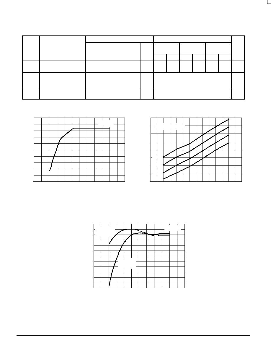
* For output pulse widths greater than 100
µ
s, typically
= kRxCx, where the value of k may be found in Figure 1.
Figure 1. Typical Output Pulse Width Constant, k,
versus Supply Voltage
(For output pulse widths
>
100
µ
s:
= kRxCx)
Figure 2. Output Pulse Width versus
Timing Capacitance
Figure 3. Normalized Output Pulse Width
versus Power Supply Voltage
0.8
0.7
0.6
0.5
0.4
0.3
10 s
1 s
100 ms
10 ms
1 ms
100
µ
s
10
µ
s
1
µ
s
100 ns
1.1
1
0.9
0.8
0.7
0.6
0.5
1
2
3
4
5
6
7
0.00001 0.0001
0.001
0.01
0.1
1
10
100
1
2
3
4
5
6
7
VCC, POWER SUPPLY VOLTAGE (VOLTS)
CAPACITANCE (
µ
F)
VCC, POWER SUPPLY VOLTAGE (VOLTS)
k, OUTPUT
PULSE WIDTH CONST
ANT
(TYPICAL)
OUTPUT
PULSE WIDTH (
)
OUTPUT
PULSE WIDTH (t)
(NORMALIZED
T
O 5 V NUMBER)
TA = 25
∞
C
VCC = 5 V, TA = 25
∞
C
1 M
100 k
10 k
1 k
TA = 25
∞
C
Rx = 100 k
Cx = 1000 pF
Rx = 1 M
Cx = 0.1
µ
F
MC54/74HC4538A
MOTOROLA
High≠Speed CMOS Logic Data
DL129 -- Rev 6
3≠6
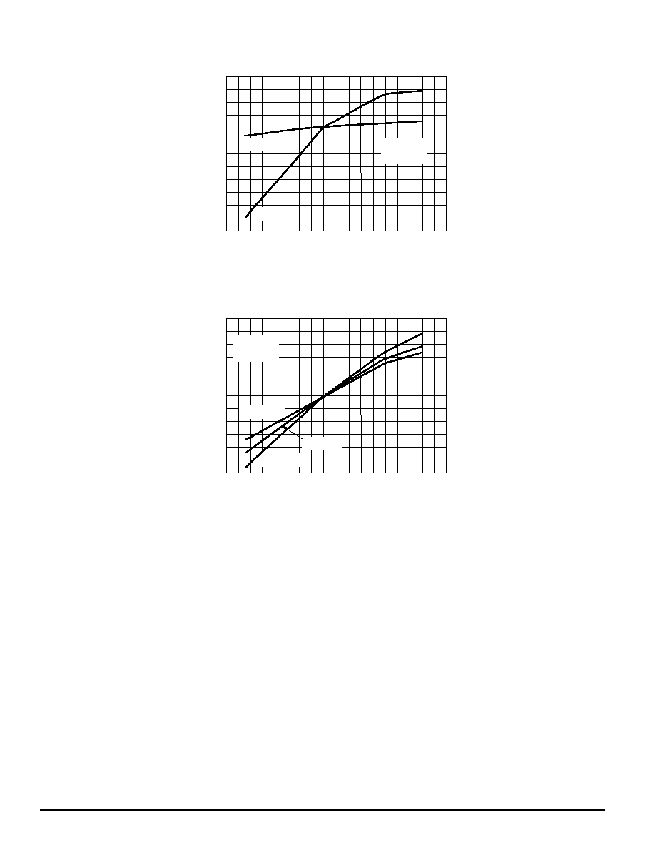
Figure 4. Normalized Output Pulse Width
versus Power Supply Voltage
Figure 5. Normalized Output Pulse Width
versus Power Supply Voltage
1.1
1.05
1
0.95
0.9
0.85
0.8
1.03
1.02
1.01
1
0.99
0.98
0.97
≠ 75
≠ 50
≠ 25
0
25
50
75
100
125
150
≠ 75
≠ 50
≠ 25
0
25
50
75
100
125
150
TA, AMBIENT TEMPERATURE (
∞
C)
TA, AMBIENT TEMPERATURE (
∞
C)
OUTPUT
PULSE WIDTH (
)
(NORMALIZED
T
O 25
C NUMBER)
∞
Rx = 10 k
Cx = 0.1
µ
F
VCC = 6 V
VCC = 3 V
Rx = 10 k
Cx = 0.1
µ
F
VCC = 5.5 V
VCC = 4.5 V
VCC = 5 V
OUTPUT
PULSE WIDTH (
)
(NORMALIZED
T
O 25
C NUMBER)
∞
MC54/74HC4538A
High≠Speed CMOS Logic Data
DL129 -- Rev 6
3≠7
MOTOROLA
SWITCHING WAVEFORMS
Figure 6.
A
B
Q
Q
A
B
RESET
Q
Q
50%
tPLH
50%
50%
tPLH
50%
GND
VCC
GND
VCC
tr
tf
90%
10%
tf
tTLH
tTHL
90%
10%
90%
10%
tPLH
tPHL
50%
50%
tf
90%
10%
50%
50%
(RETRIGGERED PULSE)
50%
GND
VCC
GND
VCC
GND
VCC
tw(H)
tw(L)
tw(L)
trec
+ trr
trr
tPHL
tPHL
Figure 7.
* Includes all probe and jig capacitance
Figure 8. Test Circuit
CL*
TEST POINT
DEVICE
UNDER
TEST
OUTPUT
MC54/74HC4538A
MOTOROLA
High≠Speed CMOS Logic Data
DL129 -- Rev 6
3≠8
PIN DESCRIPTIONS
INPUTS
A1, A2 (Pins 4, 12)
Positive≠edge trigger inputs. A rising≠edge signal on
either of these pins triggers the corresponding multivibrator
when there is a high level on the B1 or B2 input.
B1, B2 (Pins 5, 11)
Negative≠edge trigger inputs. A falling≠edge signal on
either of these pins triggers the corresponding multivibrator
when there is a low level on the A1 or A2 input.
Reset 1, Reset 2 (Pins 3, 13)
Reset inputs (active low). When a low level is applied to
one of these pins, the Q output of the corresponding multi-
vibrator is reset to a low level and the Q output is set to a high
level.
CX1/RX1 and CX2/RX2 (Pins 2 and 14)
External timing components. These pins are tied to the
common points of the external timing resistors and capaci-
tors (see the Block Diagram). Polystyrene capacitors are
recommended for optimum pulse width control. Electrolytic
capacitors are not recommended due to high leakages
associated with these type capacitors.
GND (Pins 1 and 15)
External ground. The external timing capacitors discharge
to ground through these pins.
OUTPUTS
Q1, Q2 (Pins 6, 10)
Noninverted monostable outputs. These pins (normally
low) pulse high when the multivibrator is triggered at either
the A or the B input. The width of the pulse is determined by
the external timing components, RX and CX.
Q1, Q2 (Pins 7, 9)
Inverted monostable outputs. These pins (normally high)
pulse low when the multivibrator is triggered at either the A or
the B input. These outputs are the inverse of Q1 and Q2.
+
≠
+
≠
Figure 9.
RxCx
VCC
M1
2 k
M3
M2
A
B
RESET
POWER
ON
RESET
RESET LATCH
TRIGGER CONTROL
RESET CIRCUIT
TRIGGER CONTROL
CIRCUIT
OUTPUT
LATCH
UPPER
REFERENCE
CIRCUIT
Vre, UPPER
LOWER
REFERENCE
CIRCUIT
Vre, LOWER
Q
Q
C
CB
Q
R
VCC
LOGIC DETAIL
(1/2 THE DEVICE)
MC54/74HC4538A
High≠Speed CMOS Logic Data
DL129 -- Rev 6
3≠9
MOTOROLA
CIRCUIT OPERATION
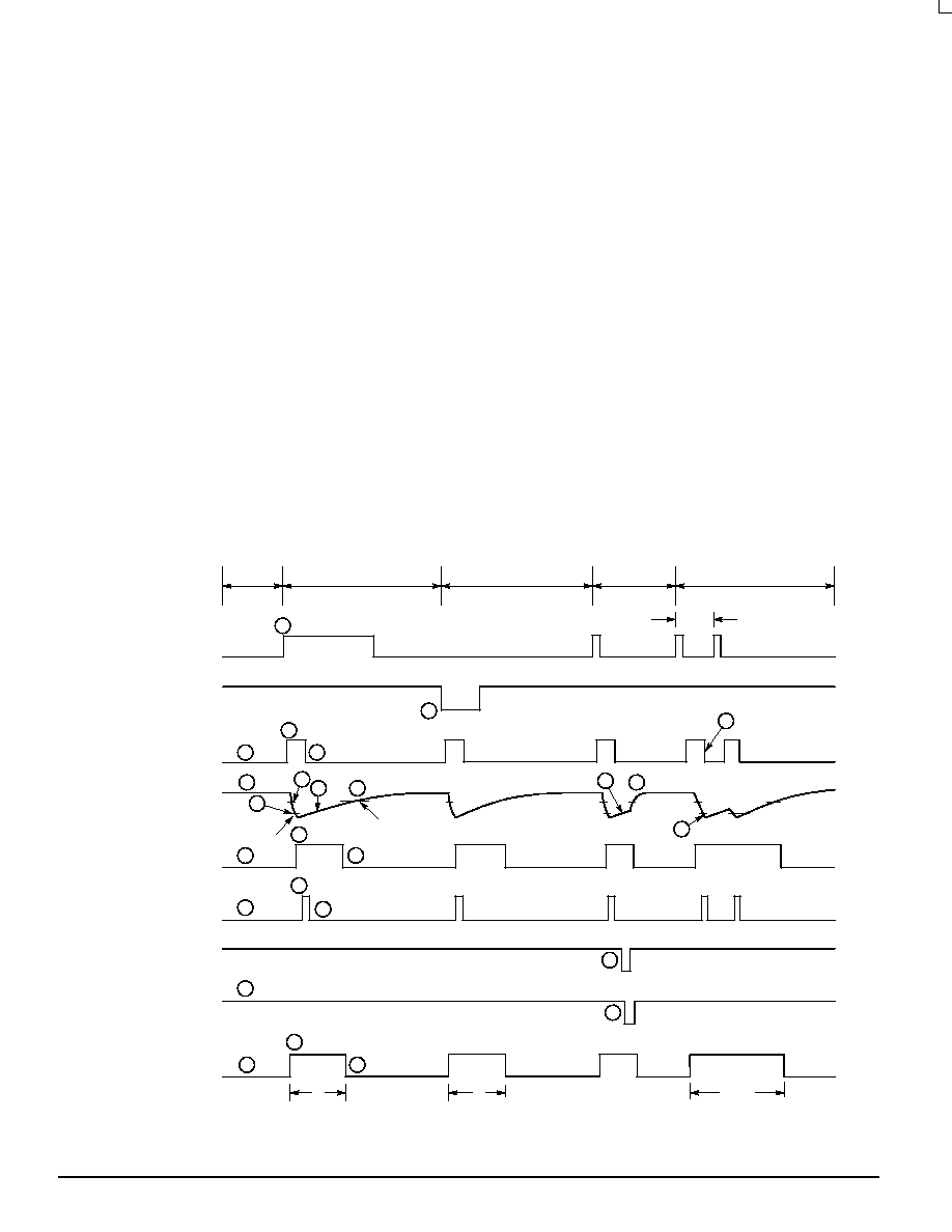
Figure 12 shows the HC4538A configured in the retrigger-
able mode. Briefly, the device operates as follows (refer to
Figure 10): In the quiescent state, the external timing capac-
itor, Cx, is charged to VCC. When a trigger occurs, the Q out-
put goes high and Cx discharges quickly to the lower
reference voltage (Vref Lower
[
1/3 VCC). Cx then charges,
through Rx, back up to the upper reference voltage (Vref Up-
per
[
2/3 VCC), at which point the one≠shot has timed out
and the Q output goes low.
The following, more detailed description of the circuit op-
eration refers to both the logic detail (Figure 9) and the timing
diagram (Figure 10).
QUIESCENT STATE
In the quiescent state, before an input trigger appears, the
output latch is high and the reset latch is high (#1 in Fig-
ure 10). Thus the Q output (pin 6 or 10) of the monostable
multivibrator is low (#2, Figure 10).
The output of the trigger≠control circuit is low (#3), and
transistors M1, M2, and M3 are turned off. The external tim-
ing capacitor, Cx, is charged to VCC (#4), and both the upper
and lower reference circuit has a low output (#5).
In addition, the output of the trigger≠control reset circuit is
low.
TRIGGER OPERATION
The HC4538A is triggered by either a rising≠edge signal at
input A (#7) or a falling≠edge signal at input B (#8), with the
unused trigger input and the Reset input held at the voltage
levels shown in the Function Table. Either trigger signal will
cause the output of the trigger≠control circuit to go high (#9).
The trigger≠control circuit going high simultaneously initi-
ates two events. First, the output latch goes low, thus taking
the Q output of the HC4538A to a high state (#10). Second,
transistor M3 is turned on, which allows the external timing
capacitor, Cx, to rapidly discharge toward ground (#11).
(Note that the voltage across Cx appears at the input of both
the upper and lower reference circuit comparator).
When Cx discharges to the reference voltage of the lower
reference circuit (#12), the outputs of both reference circuits
will be high (#13). The trigger≠control reset circuit goes high,
resetting the trigger≠control circuit flip≠flop to a low state
(#14). This turns transistor M3 off again, allowing Cx to begin
to charge back up toward VCC, with a time constant t = RxCx
(#15). Once the voltage across Cx charges to above the low-
er reference voltage, the lower reference circuit will go low
allowing the monostable multivibrator to be retriggered.
2
18
1
6
5
4
17
14
3
9
8
7
QUIESCENT
STATE
TRIGGER CYCLE
(A INPUT)
TRIGGER CYCLE
(B INPUT)
RESET
RETRIGGER
trr
Vref UPPER
Vref LOWER
TRIGGER INPUT A
(PIN 4 OR 12)
TRIGGER INPUT B
(PIN 5 OR 11)
TRIGGER-CONTROL
CIRCUIT OUTPUT
RX/CX INPUT
(PIN 2 OR 14)
UPPER REFERENCE
CIRCUIT
LOWER REFERENCE
CIRCUIT
RESET INPUT
(PIN 3 OR 13)
RESET LATCH
Q OUTPUT
(PIN 6 OR 10)
Figure 10. Timing Diagram
10
11
12
13
15
16
19
20
21
22
23
24
25
+ trr
13
MC54/74HC4538A
MOTOROLA
High≠Speed CMOS Logic Data
DL129 -- Rev 6
3≠10
When Cx charges up to the reference voltage of the upper
reference circuit (#17), the output of the upper reference cir-
cuit goes low (#18). This causes the output latch to toggle,
taking the Q output of the HC4538A to a low state (#19), and
completing the time≠out cycle.
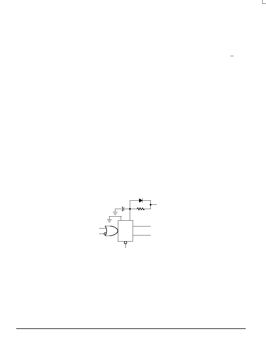
POWER≠DOWN CONSIDERATIONS
Large values of Cx may cause problems when powering
down the HC4538A because of the amount of energy stored
in the capacitor. When a system containing this device is
powered down, the capacitor may discharge from VCC
through the input protection diodes at pin 2 or pin 14. Current
through the protection diodes must be limited to 30 mA;
therefore, the turn≠off time of the VCC power supply must not
be faster than t = V C C
C x /(30 mA). For example, if
VCC = 5.0 V and Cx = 15
µ
F, the VCC supply must turn off no
faster than t = (5.0 V)
(15
µ
F)/30 mA = 2.5 ms. This is usually
not a problem because power supplies are heavily filtered
and cannot discharge at this rate.
When a more rapid decrease of VCC to zero volts occurs,
the HC4538A may sustain damage. To avoid this possibility,
use an external damping diode, Dx, connected as shown in
Figure 11. Best results can be achieved if diode Dx is chosen
to be a germanium or Schottky type diode able to withstand
large current surges.
RESET AND POWER ON RESET OPERATION
A low voltage applied to the Reset pin always forces the Q
output of the HC4538A to a low state.
The timing diagram illustrates the case in which reset oc-
curs (#20) while Cx is charging up toward the reference volt-
age of the upper reference circuit (#21). When a reset
occurs, the output of the reset latch goes low (#22), turning
on transistor M1. Thus Cx is allowed to quickly charge up to
VCC (#23) to await the next trigger signal.
On power up of the HC4538A the power≠on reset circuit
will be high causing a reset condition. This will prevent the
trigger≠control circuit from accepting a trigger input during
this state. The HC4538A's Q outputs are low and the Q not
outputs are high.
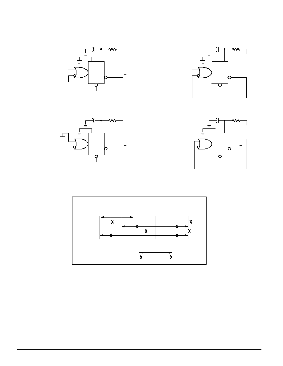
RETRIGGER OPERATION
When used in the retriggerable mode (Figure 12), the
HC4538A may be retriggered during timing out of the output
pulse at any time after the trigger≠control circuit flip≠flop has
been reset (#24), and the voltage across Cx is above the low-
er reference voltage. As long as the Cx voltage is below the
lower reference voltage, the reset of the flip≠flop is high, dis-
abling any trigger pulse. This prevents M3 from turning on
during this period resulting in an output pulse width that is
predictable.
The amount of undershoot voltage on RxCx during the
trigger mode is a function of loop delay, M3 conductivity, and
VDD. Minimum retrigger time, trr (Figure 7), is a function of
1) time to discharge RxCx from VDD to lower reference
voltage (Tdischarge); 2) loop delay (Tdelay); 3) time to charge
RxCx from the undershoot voltage back to the lower refer-
ence voltage (Tcharge).
Figure 13 shows the device configured in the non≠retrig-
gerable mode.
An Application Note (AN1558/D) titled
Characterization of
Retrigger Time in the HC4538A Dual Precision Monstable
Multivibrator is being prepared. Please consult the factory for
its availability.
DX
CX
VCC
Q
Q
RESET
A
B
Figure 11. Discharge Protection During Power Down
RX
MC54/74HC4538A
High≠Speed CMOS Logic Data
DL129 -- Rev 6
3≠11
MOTOROLA
TYPICAL APPLICATIONS
RESET = VCC
RISING≠EDGE
TRIGGER
B = VCC
RESET = VCC
RISING≠EDGE
TRIGGER
A = GND
RESET = VCC
FALLING≠EDGE
TRIGGER
RESET = VCC
FALLING≠EDGE
TRIGGER
Figure 12. Retriggerable Monostable Circuitry
Figure 13. Non≠retriggerable Monostable Circuitry
CX
VCC
Q
Q
A
B
RX
CX
VCC
Q
Q
A
B
RX
CX
VCC
Q
Q
B
RX
CX
VCC
Q
Q
A
B
RX
ONE≠SHOT SELECTION GUIDE
100 ns
1
µ
s
10
µ
s 100
µ
s 1 ms
10 ms 100 ms
1 s
10 s
MC14528B
MC14536B
MC14538B
MC14541B
HC4538A*
* Limited operating voltage (2 ≠ 6 V)
23 HR
5 MIN
TOTAL OUTPUT PULSE WIDTH RANGE
RECOMMENDED PULSE WIDTH RANGE
MC54/74HC4538A
MOTOROLA
High≠Speed CMOS Logic Data
DL129 -- Rev 6
3≠12
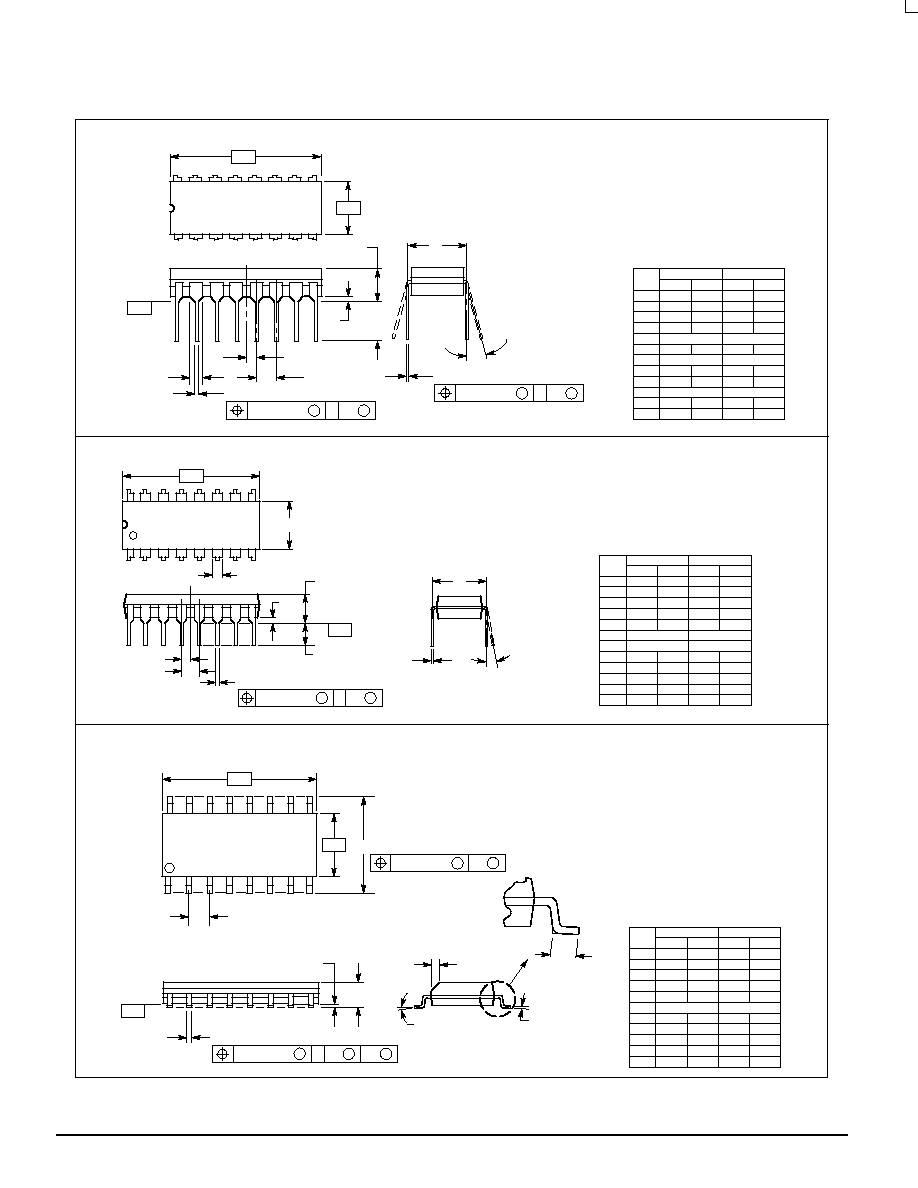
OUTLINE DIMENSIONS
J SUFFIX
CERAMIC PACKAGE
CASE 620≠10
ISSUE V
N SUFFIX
PLASTIC PACKAGE
CASE 648≠08
ISSUE R
19.05
6.10
--
0.39
1.40
0.21
3.18
19.93
7.49
5.08
0.50
1.65
0.38
4.31
0
∞
0.51
15
∞
1.01
1.27 BSC
2.54 BSC
7.62 BSC
MIN
MIN
MAX
MAX
INCHES
MILLIMETERS
DIM
0.750
0.240
--
0.015
0.055
0.008
0.125
0.785
0.295
0.200
0.020
0.065
0.015
0.170
0.050 BSC
0.100 BSC
0.300 BSC
A
B
C
D
E
F
G
J
K
L
M
N
0
∞
0.020
15
∞
0.040
NOTES:
1. DIMENSIONING AND TOLERANCING PER
ANSI Y14.5M, 1982.
2. CONTROLLING DIMENSION: INCH.
3. DIMENSION L TO CENTER OF LEAD WHEN
FORMED PARALLEL.
4. DIM F MAY NARROW TO 0.76 (0.030) WHERE
THE LEAD ENTERS THE CERAMIC BODY.
1
8
9
16
≠A
≠
≠B
≠
C
K
N
G
E
F
D
16 PL
≠T
≠
SEATING
PLANE
M
L
J
16 PL
0.25 (0.010)
T
A
M
S
0.25 (0.010)
T
B
M
S
MIN
MIN
MAX
MAX
INCHES
MILLIMETERS
DIM
A
B
C
D
F
G
H
J
K
L
M
S
18.80
6.35
3.69
0.39
1.02
0.21
2.80
7.50
0
∞
0.51
19.55
6.85
4.44
0.53
1.77
0.38
3.30
7.74
10
∞
1.01
0.740
0.250
0.145
0.015
0.040
0.008
0.110
0.295
0
∞
0.020
0.770
0.270
0.175
0.021
0.070
0.015
0.130
0.305
10
∞
0.040
NOTES:
1. DIMENSIONING AND TOLERANCING PER ANSI
Y14.5M, 1982.
2. CONTROLLING DIMENSION: INCH.
3. DIMENSION L TO CENTER OF LEADS WHEN
FORMED PARALLEL.
4. DIMENSION B DOES NOT INCLUDE MOLD FLASH.
5. ROUNDED CORNERS OPTIONAL.
2.54 BSC
1.27 BSC
0.100 BSC
0.050 BSC
≠A
≠
B
1
8
9
16
F
H
G
D
16 PL
S
C
≠T
≠
SEATING
PLANE
K
J
M
L
T
A
0.25 (0.010)
M
M
0.25 (0.010)
T
B
A
M
S
S
MIN
MIN
MAX
MAX
MILLIMETERS
INCHES
DIM
A
B
C
D
F
G
J
K
M
P
R
9.80
3.80
1.35
0.35
0.40
0.19
0.10
0
∞
5.80
0.25
10.00
4.00
1.75
0.49
1.25
0.25
0.25
7
∞
6.20
0.50
0.386
0.150
0.054
0.014
0.016
0.008
0.004
0
∞
0.229
0.010
0.393
0.157
0.068
0.019
0.049
0.009
0.009
7
∞
0.244
0.019
1.27 BSC
0.050 BSC
NOTES:
1. DIMENSIONING AND TOLERANCING PER ANSI
Y14.5M, 1982.
2. CONTROLLING DIMENSION: MILLIMETER.
3. DIMENSIONS A AND B DO NOT INCLUDE
MOLD PROTRUSION.
4. MAXIMUM MOLD PROTRUSION 0.15 (0.006)
PER SIDE.
5. DIMENSION D DOES NOT INCLUDE DAMBAR
PROTRUSION. ALLOWABLE DAMBAR
PROTRUSION SHALL BE 0.127 (0.005) TOTAL
IN EXCESS OF THE D DIMENSION AT
MAXIMUM MATERIAL CONDITION.
1
8
9
16
≠A
≠
≠B
≠
D
16 PL
K
C
G
≠T
≠
SEATING
PLANE
R
X 45
∞
M
J
F
P
8 PL
0.25 (0.010)
B
M
M
D SUFFIX
PLASTIC SOIC PACKAGE
CASE 751B≠05
ISSUE J
MC54/74HC4538A
High≠Speed CMOS Logic Data
DL129 -- Rev 6
3≠13
MOTOROLA
How to reach us:
USA/EUROPE: Motorola Literature Distribution;
JAPAN: Nippon Motorola Ltd.; Tatsumi≠SPD≠JLDC, Toshikatsu Otsuki,
P.O. Box 20912; Phoenix, Arizona 85036. 1≠800≠441≠2447
6F Seibu≠Butsuryu≠Center, 3≠14≠2 Tatsumi Koto≠Ku, Tokyo 135, Japan. 03≠3521≠8315
MFAX: RMFAX0@email.sps.mot.com ≠TOUCHTONE (602) 244≠6609
HONG KONG: Motorola Semiconductors H.K. Ltd.; 8B Tai Ping Industrial Park,
INTERNET: http://Design≠NET.com
51 Ting Kok Road, Tai Po, N.T., Hong Kong. 852≠26629298
Motorola reserves the right to make changes without further notice to any products herein. Motorola makes no warranty, representation or guarantee regarding
the suitability of its products for any particular purpose, nor does Motorola assume any liability arising out of the application or use of any product or circuit,
and specifically disclaims any and all liability, including without limitation consequential or incidental damages. "Typical" parameters can and do vary in different
applications. All operating parameters, including "Typicals" must be validated for each customer application by customer's technical experts. Motorola does
not convey any license under its patent rights nor the rights of others. Motorola products are not designed, intended, or authorized for use as components in
systems intended for surgical implant into the body, or other applications intended to support or sustain life, or for any other application in which the failure of
the Motorola product could create a situation where personal injury or death may occur. Should Buyer purchase or use Motorola products for any such
unintended or unauthorized application, Buyer shall indemnify and hold Motorola and its officers, employees, subsidiaries, affiliates, and distributors harmless
against all claims, costs, damages, and expenses, and reasonable attorney fees arising out of, directly or indirectly, any claim of personal injury or death
associated with such unintended or unauthorized use, even if such claim alleges that Motorola was negligent regarding the design or manufacture of the part.
Motorola and
are registered trademarks of Motorola, Inc. Motorola, Inc. is an Equal Opportunity/Affirmative Action Employer.
MC54/74HC4538A/D
*MC54/74HC4538A/D*
CODELINE