 | –≠–ª–µ–∫—Ç—Ä–æ–Ω–Ω—ã–π –∫–æ–º–ø–æ–Ω–µ–Ω—Ç: 74LS195 | –°–∫–∞—á–∞—Ç—å:  PDF PDF  ZIP ZIP |

5-366
FAST AND LS TTL DATA
UNIVERSAL 4-BIT
SHIFT REGISTER
The SN54 / 74LS195A is a high speed 4-Bit Shift Register offering typical
shift frequencies of 39 MHz. It is useful for a wide variety of register and
counting applications. It utilizes the Schottky diode clamped process to
achieve high speeds and is fully compatible with all Motorola TTL products.
∑
Typical Shift Right Frequency of 39 MHz
∑
Asynchronous Master Reset
∑
J, K Inputs to First Stage
∑
Fully Synchronous Serial or Parallel Data Transfers
∑
Input Clamp Diodes Limit High Speed Termination Effects
CONNECTION DIAGRAM DIP (TOP VIEW)
NOTE:
The Flatpak version
has the same pinouts
(Connection Diagram) as
the Dual In-Line Package.
14
13
12
11
10
9
1
2
3
4
5
6
7
16
15
8
VCC
MR
Q0
Q1
Q2
Q3
CP
Q3
PE
J
K
P0
P1
P2
P3 GND
PIN NAMES
LOADING (Note a)
HIGH
LOW
PE
Parallel Enable (Active LOW) Input
0.5 U.L.
0.25 U.L.
P0 ≠ P3
Parallel Data Inputs
0.5 U.L.
0.25 U.L.
J
First Stage J (Active HIGH) Input
0.5 U.L.
0.25 U.L.
K
First Stage K (Active LOW) Input
0.5 U.L.
0.25 U.L.
CP
Clock (Active HIGH Going Edge) Input
0.5 U.L.
0.25 U.L.
MR
Master Reset (Active LOW) Input
0.5 U.L.
0.25 U.L.
Q0 ≠ Q3
Parallel Outputs (Note b)
10 U.L.
5 (2.5) U.L.
Q3
Complementary Last Stage Output (Note b)
10 U.L.
5 (2.5) U.L.
NOTES:
a. 1 TTL Unit Load (U.L.) = 40
µ
A HIGH/1.6 mA LOW.
b. The Output LOW drive factor is 2.5 U.L. for Military (54) and 5 U.L. for Commercial (74)
b.
Temperature Ranges.
SN54/74LS195A
UNIVERSAL 4-BIT
SHIFT REGISTER
LOW POWER SCHOTTKY
J SUFFIX
CERAMIC
CASE 620-09
N SUFFIX
PLASTIC
CASE 648-08
16
1
16
1
ORDERING INFORMATION
SN54LSXXXJ
Ceramic
SN74LSXXXN
Plastic
SN74LSXXXD
SOIC
16
1
D SUFFIX
SOIC
CASE 751B-03
LOGIC SYMBOL
2
10
3
4 5 6 7
11
12
13
14
15
1
9
J
PE
CP
K MR
P0 P1 P2 P3
Q0 Q1 Q2 Q3
Q3
VCC = PIN 16
GND = PIN 8

5-367
FAST AND LS TTL DATA
SN54/74LS195A
LOGIC DIAGRAM
J
P0
P1
P2
P3
CP
PE
K
MR
Q0
Q0
Q1
Q3
R
CP
S
CD
Q0
Q2
Q3
14
1
2
6
7
3
4
5
9
11
12
10
13
15
VCC = PIN 16
GND = PIN 8
= PIN NUMBERS
R
CP
S
CD
Q0
R
CP
S
CD
Q2
Q3
R
CP
S
CD
Q3
FUNCTIONAL DESCRIPTION
The Logic Diagram and Truth Table indicate the functional
characteristics of the LS195A 4-Bit Shift Register. The device
is useful in a wide variety of shifting, counting and storage
applications. It performs serial, parallel, serial to parallel, or
parallel to serial data transfers at very high speeds.
The LS195A has two primary modes of operation, shift right
(Q0 Q1) and parallel load which are controlled by the state of
the Parallel Enable (PE) input. When the PE input is HIGH,
serial data enters the first flip-flop Q0 via the J and K inputs and
is shifted one bit in the direction Q0 Q1 Q2 Q3 following
each LOW to HIGH clock transition. The JK inputs provide the
flexibility of the JK type input for special applications, and the
simple D type input for general applications by tying the two
pins together. When the PE input is LOW, the LS195A appears
as four common clocked D flip-flops. The data on the parallel
inputs P0, P1, P2, P3 is transferred to the respective Q0, Q1,
Q2, Q3 outputs following the LOW to HIGH clock transition.
Shift left operations (Q3 Q2) can be achieved by tying the Qn
Outputs to the Pn≠1 inputs and holding the PE input LOW.
All serial and parallel data transfers are synchronous,
occurring after each LOW to HIGH clock transition. Since the
LS195A utilizes edge-triggering, there is no restriction on the
activity of the J, K, Pn and PE inputs for logic operation --
except for the set-up and release time requirements.
A LOW on the asynchronous Master Reset (MR) input sets
all Q outputs LOW, independent of any other input condition.
MODE SELECT -- TRUTH TABLE
OPERATING MODES
INPUTS
OUTPUTS
OPERATING MODES
MR
PE
J
K
Pn
Q0
Q1
Q2
Q3
Q3
Asynchronous Reset
L
X
X
X
X
L
L
L
L
H
Shift, Set First Stage
H
h
h
h
X
H
q0
q1
q2
q2
Shift, Reset First
H
h
I
I
X
L
q0
q1
q2
q2
Shift, Toggle First Stage
H
h
h
I
X
q0
q0
q1
q2
q2
Shift, Retain First Stage
H
h
I
h
X
q0
q0
q1
q2
q2
Parallel Load
H
I
X
X
pn
p0
p1
p2
p3
p3
L = LOW voltage levels
H = HIGH voltage levels
X = Don't Care
I = LOW voltage level one set-up time prior to the LOW to HIGH clock transition.
h = HIGH voltage level one set-up time prior to the LOW to HIGH clock transition.
pn (qn) = Lower case letters indicate the state of the referenced input (or output) one set-up time prior to the LOW to
HIGH clock transition.
5-368
FAST AND LS TTL DATA
SN54/74LS195A
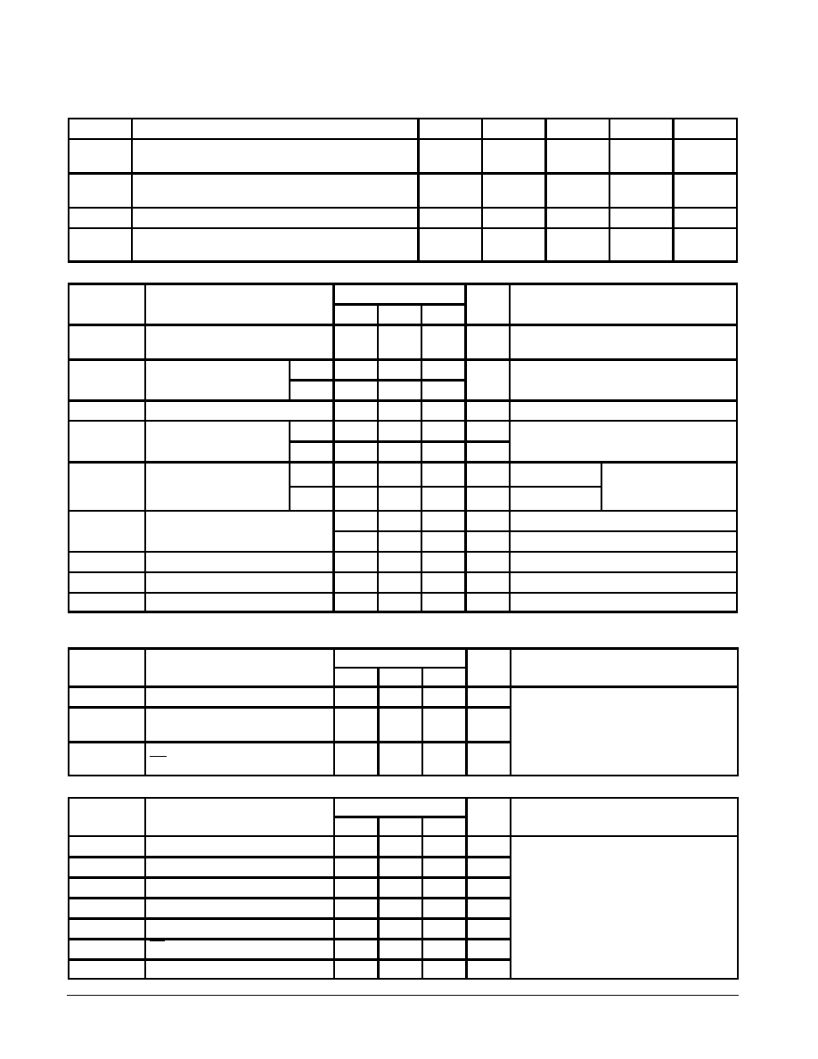
GUARANTEED OPERATING RANGES
Symbol
Parameter
Min
Typ
Max
Unit
VCC
Supply Voltage
54
74
4.5
4.75
5.0
5.0
5.5
5.25
V
TA
Operating Ambient Temperature Range
54
74
≠ 55
0
25
25
125
70
∞
C
IOH
Output Current -- High
54, 74
≠ 0.4
mA
IOL
Output Current -- Low
54
74
4.0
8.0
mA
DC CHARACTERISTICS OVER OPERATING TEMPERATURE RANGE
(unless otherwise specified)
Symbol
Parameter
Limits
Unit
Test Conditions
Symbol
Parameter
Min
Typ
Max
Unit
Test Conditions
VIH
Input HIGH Voltage
2.0
V
Guaranteed Input HIGH Voltage for
All Inputs
VIL
Input LOW Voltage
54
0.7
V
Guaranteed Input LOW Voltage for
All Inputs
VIL
Input LOW Voltage
74
0.8
V
Guaranteed Input LOW Voltage for
All Inputs
VIK
Input Clamp Diode Voltage
≠ 0.65
≠ 1.5
V
VCC = MIN, IIN = ≠ 18 mA
VOH
Output HIGH Voltage
54
2.5
3.5
V
VCC = MIN, IOH = MAX, VIN = VIH
or VIL per Truth Table
VOH
Output HIGH Voltage
74
2.7
3.5
V
VCC = MIN, IOH = MAX, VIN = VIH
or VIL per Truth Table
VOL
Output LOW Voltage
54, 74
0.25
0.4
V
IOL = 4.0 mA
VCC = VCC MIN,
VIN = VIL or VIH
per Truth Table
VOL
Output LOW Voltage
74
0.35
0.5
V
IOL = 8.0 mA
VIN = VIL or VIH
per Truth Table
IIH
Input HIGH Current
20
µ
A
VCC = MAX, VIN = 2.7 V
IIH
Input HIGH Current
0.1
mA
VCC = MAX, VIN = 7.0 V
IIL
Input LOW Current
≠ 0.4
mA
VCC = MAX, VIN = 0.4 V
IOS
Short Circuit Current (Note 1)
≠ 20
≠ 100
mA
VCC = MAX
ICC
Power Supply Current
21
mA
VCC = MAX
Note 1: Not more than one output should be shorted at a time, nor for more than 1 second.
AC CHARACTERISTICS
(TA = 25
∞
C)
Symbol
Parameter
Limits
Unit
Test Conditions
Symbol
Parameter
Min
Typ
Max
Unit
Test Conditions
fMAX
Maximum Clock Frequency
30
39
MHz
VCC = 5.0 V
CL = 15 pF
tPLH
tPHL
Propagation Delay,
Clock to Output
14
17
22
26
ns
VCC = 5.0 V
CL = 15 pF
tPHL
Propagation Delay,
MR to Output
19
30
ns
CL = 15 pF
AC SETUP REQUIREMENTS
(TA = 25
∞
C)
Symbol
Parameter
Limits
Unit
Test Conditions
Symbol
Parameter
Min
Typ
Max
Unit
Test Conditions
tW
CP Clock Pulse Width
16
ns
VCC = 5.0 V
tW
MR Pulse Width
12
ns
VCC = 5.0 V
ts
PE Setup Time
25
ns
VCC = 5.0 V
ts
Data Setup Time
15
ns
VCC = 5.0 V
trec
Recovery Time
25
ns
CC = 5.0 V
trel
PE Release Time
10
ns
th
Data Hold Time
0
ns

5-369
FAST AND LS TTL DATA
SN54/74LS195A
DEFINITIONS OF TERMS
SETUP TIME(ts) --is defined as the minimum time required
for the correct logic level to be present at the logic input prior
to the clock transition from LOW to HIGH in order to be
recognized and transferred to the outputs.
HOLD TIME (th) -- is defined as the minimum time following
the clock transition from LOW to HIGH that the logic level must
be maintained at the input in order to ensure continued
recognition. A negative HOLD TIME indicates that the correct
logic level may be released prior to the clock transition from
LOW to HIGH and still be recognized.
RECOVERY TIME (trec) -- is defined as the minimum time
required between the end of the reset pulse and the clock
transition from LOW to HIGH in order to recognize and transfer
HIGH Data to the Q outputs.
AC WAVEFORMS
The shaded areas indicate when the input is permitted to change for predictable output performance.
Figure 1. Clock to Output Delays and
Clock Pulse Width
Figure 3. Setup (ts) and Hold (th) Time for Serial Data
(J & K) and Parallel Data (P0, P1, P2, P3)
Figure 2. Master Reset Pulse Width, Master Reset
to Output Delay and Master Reset to Clock
Recovery Time
Figure 4. Setup (ts) and Hold (th) Time for PE Input
CONDITIONS: MR = H
*Q0 STATE WILL BE DETERMINED BY J AND K INPUTS .
1.3 V
1.3 V
1.3 V
1.3 V
CLOCK
OUTPUT
PE
Qn = Pn
Qn* = Qn-1
trel
trel
ts(L)
ts(H)
LOAD PARALLEL DATA
LOAD SERIAL DATA
SHIFT RIGHT
1.3 V
CONDITIONS: PE = L
PO = P1 = P2 = P3 = H
CONDITIONS: MR = H
*J AND K SET-UP TIME AFFECTS Q0 ONLY
PE
J & K
P0 P1 P2 P3
CLOCK
OUTPUT*
CLOCK
CLOCK
OUTPUT
OUTPUT
ts(H)
th(L) = 0
th(H) = 0
th(H) = 0
ts(H)
th(L) = 0
ts(L)
tPHL
tPLH
ts(L)
MR
trec
tPHL
1.3 V
1.3 V
1.3 V
1.3 V
1.3 V
1.3 V
1.3 V
1.3 V
1.3 V
tW
CONDITIONS: J = PE = MR = H
K = L
tW
1.3 V

5-370
FAST AND LS TTL DATA
MIN
MIN
MAX
MAX
MILLIMETERS
INCHES
DIM
A
B
C
D
F
G
J
K
M
P
R
9.80
3.80
1.35
0.35
0.40
0.19
0.10
0
∞
5.80
0.25
10.00
4.00
1.75
0.49
1.25
0.25
0.25
7
∞
6.20
0.50
0.386
0.150
0.054
0.014
0.016
0.008
0.004
0
∞
0.229
0.010
0.393
0.157
0.068
0.019
0.049
0.009
0.009
7
∞
0.244
0.019
1.27 BSC
0.050 BSC
NOTES:
1. DIMENSIONING AND TOLERANCING PER ANSI
Y14.5M, 1982.
2. CONTROLLING DIMENSION: MILLIMETER.
3. DIMENSION A AND B DO NOT INCLUDE MOLD
PROTRUSION.
4. MAXIMUM MOLD PROTRUSION 0.15 (0.006)
PER SIDE.
5. 751B 01 IS OBSOLETE, NEW STANDARD
751B 03.
1
8
9
16
-A-
-B-
P
16 PL
D
-T-
K
C
G
M
R X 45
∞
F
J
8 PL
SEATING
PLANE
Case 751B-03 D Suffix
16-Pin Plastic
SO-16
B
0.25 (0.010)
M
M
T
0.25 (0.010)
B
A
M
S
S
Case 648-08 N Suffix
16-Pin Plastic
MIN
MIN
MAX
MAX
MILLIMETERS
INCHES
DIM
A
B
C
D
F
G
H
J
K
L
M
S
18.80
6.35
3.69
0.39
1.02
0.21
2.80
7.50
0
∞
0.51
19.55
6.85
4.44
0.53
1.77
0.38
3.30
7.74
10
∞
1.01
0.740
0.250
0.145
0.015
0.040
0.008
0.110
0.295
0
∞
0.020
0.770
0.270
0.175
0.021
0.070
0.015
0.130
0.305
10
∞
0.040
NOTES:
1. DIMENSIONING AND TOLERANCING PER ANSI
Y14.5M, 1982.
2. CONTROLLING DIMENSION: INCH.
3. DIMENSION L" TO CENTER OF LEADS WHEN
FORMED PARALLEL.
4. DIMENSION B" DOES NOT INCLUDE MOLD
FLASH.
5. ROUNDED CORNERS OPTIONAL.
6. 648 01 THRU 07 OBSOLETE, NEW STANDARD
648 08.
2.54 BSC
1.27 BSC
0.100 BSC
0.050 BSC
-A-
B
1
8
9
16
F
H
G
D
16 PL
S
C
-T-
SEATING
PLANE
K
J
M
L
T A
0.25 (0.010)
M
M
Case 620-09 J Suffix
16-Pin Ceramic Dual In-Line
MIN
MIN
MAX
MAX
MILLIMETERS
INCHES
DIM
19.05
6.10
0.39
1.40
0.23
0
∞
0.39
19.55
7.36
4.19
0.53
1.77
0.27
5.08
15
∞
0.88
0.750
0.240
0.015
0.055
0.009
0
∞
0.015
0.770
0.290
0.165
0.021
0.070
0.011
0.200
15
∞
0.035
1.27 BSC
2.54 BSC
7.62 BSC
0.050 BSC
0.100 BSC
0.300 BSC
A
B
C
D
E
F
G
J
K
L
M
N
NOTES:
1. DIMENSIONING AND TOLERANCING PER ANSI
Y14.5M, 1982.
2. CONTROLLING DIMENSION: INCH.
3. DIMENSION L TO CENTER OF LEAD WHEN
FORMED PARALLEL.
4. DIM F MAY NARROW TO 0.76 (0.030) WHERE
THE LEAD ENTERS THE CERAMIC BODY.
5. 620 01 THRU 08 OBSOLETE, NEW STANDARD
620 09.
-B-
-A-
16 PL
-T-
C
D
E
F
G
J
K
M
N
SEATING
PLANE
16 PL
L
16
9
1
8
0.25 (0.010)
T A
M
S
0.25 (0.010)
T B
M
S

5-371
FAST AND LS TTL DATA
Motorola reserves the right to make changes without further notice to any products herein. Motorola makes no warranty, representation or guarantee regarding
the suitability of its products for any particular purpose, nor does Motorola assume any liability arising out of the application or use of any product or circuit,
and specifically disclaims any and all liability, including without limitation consequential or incidental damages. "Typical" parameters can and do vary in different
applications. All operating parameters, including "Typicals" must be validated for each customer application by customer's technical experts. Motorola does
not convey any license under its patent rights nor the rights of others. Motorola products are not designed, intended, or authorized for use as components in
systems intended for surgical implant into the body, or other applications intended to support or sustain life, or for any other application in which the failure of
the Motorola product could create a situation where personal injury or death may occur. Should Buyer purchase or use Motorola products for any such
unintended or unauthorized application, Buyer shall indemnify and hold Motorola and its officers, employees, subsidiaries, affiliates, and distributors harmless
against all claims, costs, damages, and expenses, and reasonable attorney fees arising out of, directly or indirectly, any claim of personal injury or death
associated with such unintended or unauthorized use, even if such claim alleges that Motorola was negligent regarding the design or manufacture of the part.
Motorola and
are registered trademarks of Motorola, Inc. Motorola, Inc. is an Equal Opportunity/Affirmative Action Employer.
Literature Distribution Centers:
USA: Motorola Literature Distribution; P.O. Box 20912; Phoenix, Arizona 85036.
EUROPE: Motorola Ltd.; European Literature Centre; 88 Tanners Drive, Blakelands, Milton Keynes, MK14 5BP, England.
JAPAN: Nippon Motorola Ltd.; 4-32-1, Nishi-Gotanda, Shinagawa-ku, Tokyo 141, Japan.
ASIA PACIFIC: Motorola Semiconductors H.K. Ltd.; Silicon Harbour Center, No. 2 Dai King Street, Tai Po Industrial Estate, Tai Po, N.T., Hong Kong.