 | –≠–ª–µ–∫—Ç—Ä–æ–Ω–Ω—ã–π –∫–æ–º–ø–æ–Ω–µ–Ω—Ç: 74LS293 | –°–∫–∞—á–∞—Ç—å:  PDF PDF  ZIP ZIP |
5-466
FAST AND LS TTL DATA
DECADE COUNTER;
4-BIT BINARY COUNTER
The SN54 / 74LS290 and SN54 / 74LS293 are high-speed 4-bit ripple type
counters partitioned into two sections. Each counter has a divide-by-two sec-
tion and either a divide-by-five (LS290) or divide-by-eight (LS293) section
which are triggered by a HIGH-to-LOW transition on the clock inputs. Each
section can be used separately or tied together (Q to CP)to form BCD,
Bi-quinary, or Modulo-16 counters. Both of the counters have a 2-input gated
Master Reset (Clear), and the LS290 also has a 2-input gated Master Set
(Preset 9).
∑
Corner Power Pin Versions of the LS90 and LS93
∑
Low Power Consumption . . . Typically 45 mW
∑
High Count Rates . . . Typically 42 MHz
∑
Choice of Counting Modes . . . BCD, Bi-Quinary, Binary
∑
Input Clamp Diodes Limit High Speed Termination Effects
14
13
12
11
10
9
1
2
3
4
5
6
8
7
VCC MR
MR
CP1 CP0 Q0
Q3
MS
NC
MS
Q2
Q1
NC GND
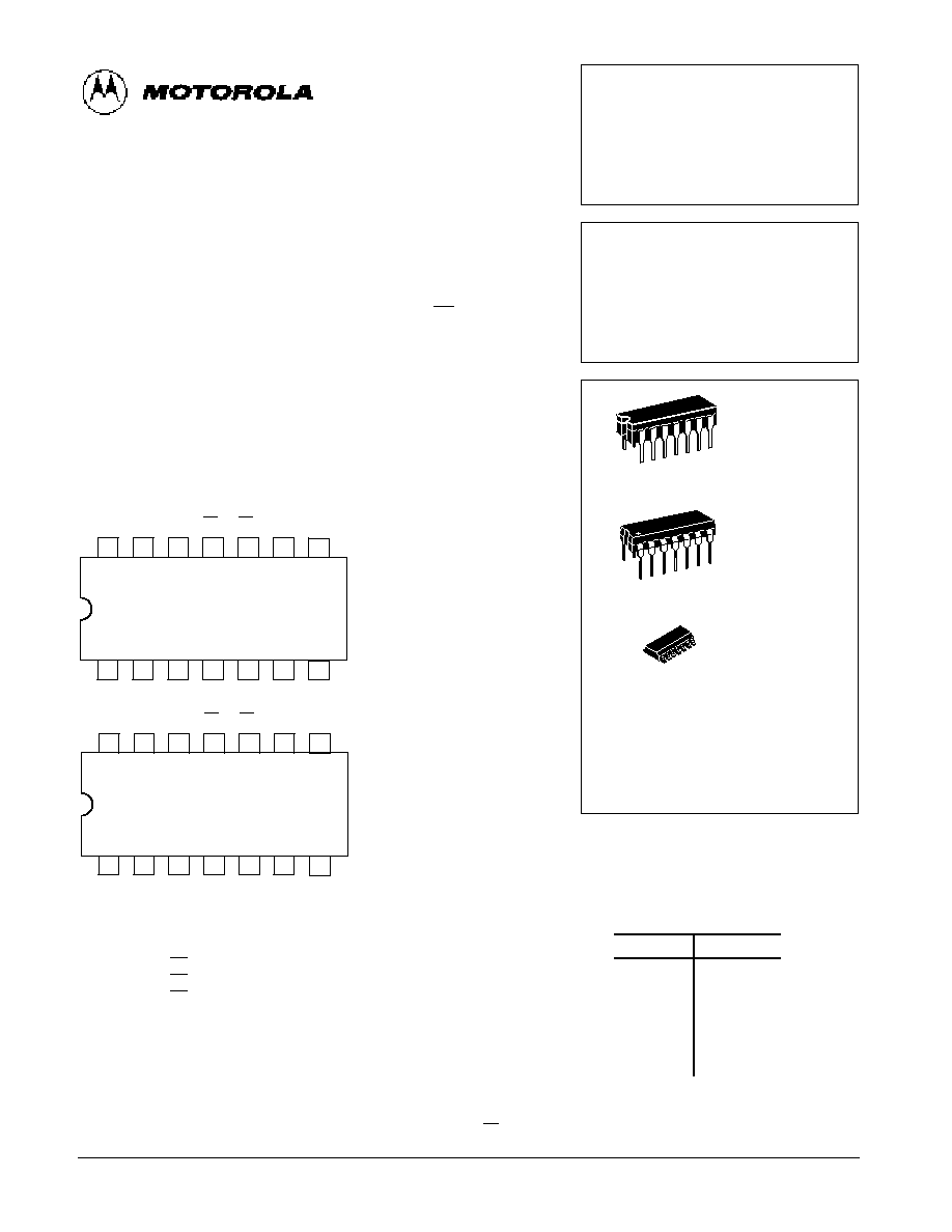
CONNECTION DIAGRAM DIP (TOP VIEW)
LS290
LS293
NOTE:
The Flatpak version
has the same pinouts
(Connection Diagram) as
the Dual In-Line Package.
14
13
12
11
10
9
1
2
3
4
5
6
8
7
VCC MR
MR
CP1 CP0 Q0
Q3
NC
NC
NC
Q2
Q1
NC GND
PIN NAMES
LOADING (Note a)
HIGH
LOW
CP0
Clock (Active LOW going edge) Input to
˜
2 Section.
0.05 U.L.
1.5 U.L.
CP1
Clock (Active LOW going edge) Input to
˜
5 Section (LS290).
0.05 U.L.
2.0 U.L.
CP1
Clock (Active LOW going edge) Input to
˜
8 Section (LS293).
0.05 U.L.
1.0 U.L.
MR1, MR2
Master Reset (Clear) Inputs
0.5 U.L.
0.25 U.L.
MS1, MS2
Master Set (Preset-9, LS290) Inputs
0.5 U.L.
0.25 U.L.
Q0
Output from
˜
2 Section (Notes b & c)
10 U.L.
5 (2.5) U.L.
Q1, Q2, Q3
Outputs from
˜
5 &
˜
8 Sections (Note b)
10 U.L.
5 (2.5) U.L.
NOTES:
a) 1 TTL Unit Load (U.L.) = 40
µ
A HIGH/1.6 mA LOW.
b) The Output LOW drive factor is 2.5 U.L. for Military (54) and 5 U.L. for Commercial (74) Temperature Ranges.
c) The Q0 Outputs are guaranteed to drive the full fan-out plus the CP1 Input of the device.
SN54/74LS290
SN54/74LS293
DECADE COUNTER;
4-BIT BINARY COUNTER
LOW POWER SCHOTTKY
ORDERING INFORMATION
SN54LSXXXJ
Ceramic
SN74LSXXXN
Plastic
SN74LSXXXD
SOIC
J SUFFIX
CERAMIC
CASE 632-08
N SUFFIX
PLASTIC
CASE 646-06
14
1
14
1
14
1
D SUFFIX
SOIC
CASE 751A-02

5-467
FAST AND LS TTL DATA
SN54/74LS290
D
SN54/74LS293
LOGIC SYMBOL
LS290
LS293
VCC = PIN 14
GND = PIN 7
NC = PINS 2, 6
1 3
1 2
1 2
10
11
MS
CP0
CP1
MR
Q0 Q1 Q2 Q3
12 13 9 5 4 8
VCC = PIN 14
GND = PIN 7
NC = PINS 1, 2, 3, 6
1 2
10
11
CP0
CP1
MR
Q0 Q1 Q2 Q3
12 13 9 5 4 8
LS290
LS293
LOGIC DIAGRAMS
SD
J
CP
CDQ
Q
J
CP
CDQ
Q
J
CP
CDQ
Q
R
CP
CDQ
Q
SD
K
S
J
CP
CD
Q
Q
K
J
CP
CD
Q
Q
K
J
CP
CD
Q
Q
K
J
CP
CD
Q
Q
K
MS1
MS2
CP0
CP1
MR1
MR2
CP0
CP1
MR1
MR2
Q0
Q1
Q2
Q3
Q0
Q1
Q2
Q3
VCC = PIN 14
GND = PIN 7
= PIN NUMBERS
VCC = PIN 14
GND = PIN 7
= PIN NUMBERS
1
3
8
4
5
9
11
12
10
13
10
13
11
12
8
4
5
9
K

5-468
FAST AND LS TTL DATA
SN54/74LS290
D
SN54/74LS293
FUNCTIONAL DESCRIPTION
The LS290 and LS293 are 4-bit ripple type Decade, and
4-Bit Binary counters respectively. Each device consists of
four master / slave flip-flops which are internally connected to
provide a divide-by-two section and a divide-by-five (LS290)
or divide-by-eight (LS293) section. Each section has a
separate clock input which initiates state changes of the
counter on the HIGH-to-LOW clock transition. State changes
of the Q outputs do not occur simultaneously because of
internal ripple delays. Therefore, decoded output signals are
subject to decoding spikes and should not be used for clocks
or strobes. The Q0 output of each device is designed and
specified to drive the rated fan-out plus the CP1 input of the
device.
A gated AND asynchronous Master Reset (MR1
MR2) is
provided on both counters which overrides the clocks and
resets (clears) all the flip-flops. A gated AND asynchronous
Master Set (MS1
MS2) is provided on the LS290 which
overrides the clocks and the MR inputs and sets the outputs to
nine (HLLH).
Since the output from the divide-by-two section is not
internally connected to the succeeding stages, the devices
may be operated in various counting modes:
LS290
A. BCD Decade (8421) Counter -- the CP1 input must be
externally connected to the Q0 output. The CP0 input
receives the incoming count and a BCD count sequence is
produced.
B. Symmetrical Bi-quinary Divide-By-Ten Counter -- The Q3
output must be externally connected to the CP0 input. The
input count is then applied to the CP1 input and a
divide-by-ten square wave is obtained at output Q0.
C. Divide-By-Two and Divide-By-Five Counter -- No external
interconnections are required. The first flip-flop is used as a
binary element for the divide-by-two function (CP0 as the
input and Q0 as the output). The CP1 input is used to obtain
binary divide-by-five operation at the Q3 output.
LS293
A. 4-Bit Ripple Counter -- The output Q0 must be externally
connected to input CP1. The input count pulses are applied
to input CP0. Simultaneous division of 2, 4, 8, and 16 are
performed at the Q0, Q1, Q2, and Q3 outputs as shown in
the truth table.
B. 3-Bit Ripple Counter -- The input count pulses are applied
to input CP1. Simultaneous frequency divisions of 2, 4, and
8 are available at the Q1, Q2, and Q3 outputs. Independent
use of the first flip-flop is available if the reset function
coincides with reset of the 3-bit ripple-through counter.
LS290 MODE SELECTION
RESET/SET INPUTS
OUTPUTS
MR1
MR2
MS1
MS2
Q0
Q1
Q2
Q3
H
H
L
X
L
L
L
L
H
H
X
L
L
L
L
L
X
X
H
H
H
L
L
H
L
X
L
X
Count
X
L
X
L
Count
L
X
X
L
Count
X
L
L
X
Count
LS290
BCD COUNT SEQUENCE
COUNT
OUTPUT
COUNT
Q0
Q1
Q2
Q3
0
L
L
L
L
1
H
L
L
L
2
L
H
L
L
3
H
H
L
L
4
L
L
H
L
5
H
L
H
L
6
L
H
H
L
7
H
H
H
L
8
L
L
L
H
9
H
L
L
H
NOTE: Output Q0 is connected to Input CP1
for BCD count.
H = HIGH Voltage Level
L = LOW Voltage Level
X = Don't Care
LS293 MODE SELECTION
RESET INPUTS
OUTPUTS
MR1
MR2
Q0
Q1
Q2
Q3
H
H
L
L
L
L
L
H
Count
H
L
Count
L
L
Count
TRUTH TABLE
COUNT
OUTPUT
COUNT
Q0
Q1
Q2
Q3
0
L
L
L
L
1
H
L
L
L
2
L
H
L
L
3
H
H
L
L
4
L
L
H
L
5
H
L
H
L
6
L
H
H
L
7
H
H
H
L
8
L
L
L
H
9
H
L
L
H
10
L
H
L
H
11
H
H
L
H
12
L
L
H
H
13
H
L
H
H
14
L
H
H
H
15
H
H
H
H
Note: Output Q0 connected to input CP1.
5-469
FAST AND LS TTL DATA
SN54/74LS290
∑
SN54/74LS293
GUARANTEED OPERATING RANGES
Symbol
Parameter
Min
Typ
Max
Unit
VCC
Supply Voltage
54
74
4.5
4.75
5.0
5.0
5.5
5.25
V
TA
Operating Ambient Temperature Range
54
74
≠ 55
0
25
25
125
70
∞
C
IOH
Output Current -- High
54, 74
≠ 0.4
mA
IOL
Output Current -- Low
54
74
4.0
8.0
mA
DC CHARACTERISTICS OVER OPERATING TEMPERATURE RANGE
(unless otherwise specified)
Symbol
Parameter
Limits
Unit
Test Conditions
Symbol
Parameter
Min
Typ
Max
Unit
Test Conditions
VIH
Input HIGH Voltage
2.0
V
Guaranteed Input HIGH Voltage for
All Inputs
VIL
Input LOW Voltage
54
0.7
V
Guaranteed Input LOW Voltage for
All Inputs
VIL
Input LOW Voltage
74
0.8
V
Guaranteed Input LOW Voltage for
All Inputs
VIK
Input Clamp Diode Voltage
≠ 0.65
≠ 1.5
V
VCC = MIN, IIN = ≠ 18 mA
VOH
Output HIGH Voltage
54
2.5
3.5
V
VCC = MIN, IOH = MAX, VIN = VIH
or VIL per Truth Table
VOH
Output HIGH Voltage
74
2.7
3.5
V
VCC = MIN, IOH = MAX, VIN = VIH
or VIL per Truth Table
VOL
Output LOW Voltage
54, 74
0.25
0.4
V
IOL = 4.0 mA
VCC = VCC MIN,
VIN = VIL or VIH
per Truth Table
VOL
Output LOW Voltage
74
0.35
0.5
V
IOL = 8.0 mA
VIN = VIL or VIH
per Truth Table
IIH
Input HIGH Current
20
µ
A
VCC = MAX, VIN = 2.7 V
IIH
Input HIGH Current
0.1
mA
VCC = MAX, VIN = 7.0 V
IIL
Input LOW Current
MS, MR
CP0
CP1 (LS290)
CP1 (LS293)
≠0.4
≠2.4
≠3.2
≠1.6
mA
VCC = MAX, VIN = 0.4 V
IOS
Short Circuit Current (Note 1)
≠20
≠ 100
mA
VCC = MAX
ICC
Power Supply Current
15
mA
VCC = MAX
Note 1: Not more than one output should be shorted at a time, nor for more than 1 second.
5-470
FAST AND LS TTL DATA
SN54/74LS290
D
SN54/74LS293
AC CHARACTERISTICS
(TA = 25
∞
C, VCC = 5.0 V, CL = 15 pF)
Symbol
Parameter
Limits
Unit
Symbol
Parameter
LS290
LS293
Unit
Symbol
Parameter
Min
Typ
Max
Min
Typ
Max
Unit
fMAX
CP0 Input Clock Frequency
32
32
MHz
fMAX
CP1 Input Clock Frequency
16
16
MHz
tPLH
tPHL
Propagation Delay,
CP0 Input to Q0 Output
10
12
16
18
10
12
16
18
ns
tPLH
tPHL
CP0 Input to Q3 Output
32
34
48
50
46
46
70
70
ns
tPLH
tPHL
CP1 Input to Q1 Output
10
14
16
21
10
14
16
21
ns
tPLH
tPHL
CP1 Input to Q2 Output
21
23
32
35
21
23
32
35
ns
tPLH
tPHL
CP1 Input to Q3 Output
21
23
32
35
34
34
51
51
ns
tPHL
MS Input to Q0 and Q3 Outputs
20
30
ns
tPHL
MS Input to Q1 and Q2 Outputs
26
40
ns
tPHL
MR Input to Any Output
26
40
26
40
ns
AC SETUP REQUIREMENTS
(TA = 25
∞
C, VCC = 5.0 V)
Symbol
Parameter
Limits
Unit
Symbol
Parameter
LS290
LS293
Unit
Symbol
Parameter
Min
Max
Min
Max
Unit
tW
CP0 Pulse Width
15
15
ns
tW
CP1 Pulse Width
30
30
ns
tW
MS Pulse Width
15
ns
tW
MR Pulse Width
15
15
ns
trec
Recovery Time MR to CP
25
25
ns
RECOVERY TIME (trec) is defined as the minimum time required between the end of the reset pulse and the clock transition form HIGH-to-LOW in order to
recognize and transfer HIGH data to the Q outputs.
Figure 1
*CP
Q
1.3 V
1.3 V
1.3 V
1.3 V
tPHL
tPLH
Figure 2
Figure 3
1.3 V
1.3 V
1.3 V
1.3 V
1.3 V
1.3 V
1.3 V
1.3 V
MR & MS
CP
Q
tPHL
tPLH
MS
CP
Q0
Q3
(LS290)
*The number of Clock Pulses required between the tPHL and tPLH measurements can be determined from the appropriate Truth Tables.
AC WAVEFORMS
tW
tW
trec
tW
trec
5-471
FAST AND LS TTL DATA
MIN
MIN
MAX
MAX
MILLIMETERS
INCHES
DIM
A
B
C
D
F
G
J
K
M
P
R
8.55
3.80
1.35
0.35
0.40
0.19
0.10
0
∞
5.80
0.25
8.75
4.00
1.75
0.49
1.25
0.25
0.25
7
∞
6.20
0.50
0.337
0.150
0.054
0.014
0.016
0.008
0.004
0
∞
0.229
0.010
0.344
0.157
0.068
0.019
0.049
0.009
0.009
7
∞
0.244
0.019
1.27 BSC
0.050 BSC
NOTES:
1. DIMENSIONS A" AND B" ARE DATUMS AND
T" IS A DATUM SURFACE.
2. DIMENSIONING AND TOLERANCING PER ANSI
Y14.5M, 1982.
3. CONTROLLING DIMENSION: MILLIMETER.
4. DIMENSION A AND B DO NOT INCLUDE MOLD
PROTRUSION.
5. MAXIMUM MOLD PROTRUSION 0.15 (0.006)
PER SIDE.
6. 751A 01 IS OBSOLETE, NEW STANDARD
751A 02.
-A-
-B-
P
G
C
K
SEATING
PLANE
14 PL
D
M
F
J
7 PL
R X 45
∞
1
7
8
14
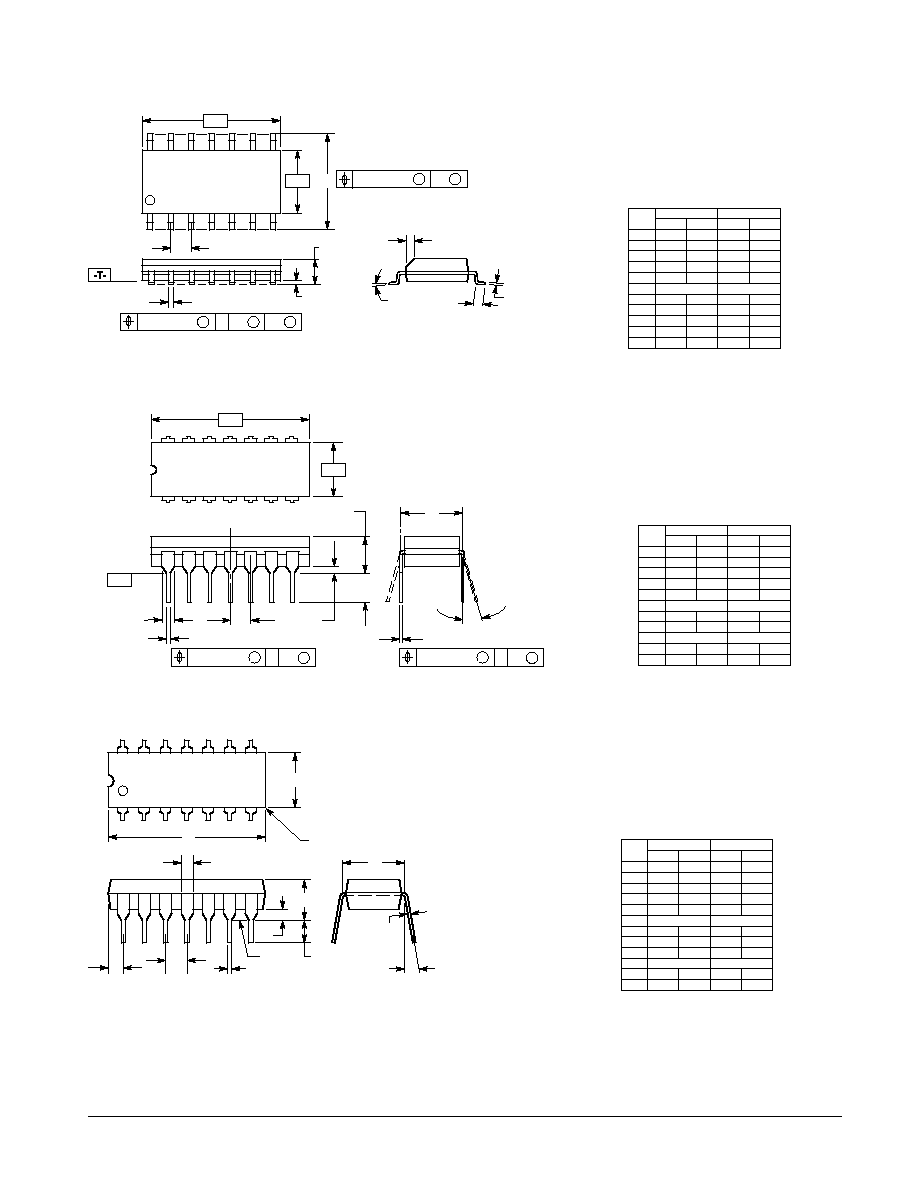
Case 751A-02 D Suffix
14-Pin Plastic
SO-14
B
0.25 (0.010)
M
M
T
0.25 (0.010)
B
A
M
S
S
Case 632-08 J Suffix
14-Pin Ceramic Dual In-Line
MIN
MIN
MAX
MAX
MILLIMETERS
INCHES
DIM
A
B
C
D
F
G
J
K
L
M
N
19.05
6.23
3.94
0.39
1.40
0.21
3.18
0
∞
0.51
19.94
7.11
5.08
0.50
1.65
0.38
4.31
15
∞
1.01
0.750
0.245
0.155
0.015
0.055
0.008
0.125
0
∞
0.020
0.785
0.280
0.200
0.020
0.065
0.015
0.170
15
∞
0.040
2.54 BSC
7.62 BSC
0.100 BSC
0.300 BSC
NOTES:
1. DIMENSIONING AND TOLERANCING PER ANSI
Y14.5M, 1982.
2. CONTROLLING DIMENSION: INCH.
3. DIMENSION L TO CENTER OF LEAD WHEN
FORMED PARALLEL.
4. DIM F MAY NARROW TO 0.76 (0.030) WHERE
THE LEAD ENTERS THE CERAMIC BODY.
5. 632 01 THRU 07 OBSOLETE, NEW STANDARD
632 08.
14
8
1
7
-A-
-B-
-T-
SEATING
PLANE
F
G
D
14 PL
N
K
C
L
J
14 PL
M
0.25 (0.010)
T A
M
S
0.25 (0.010)
T B
M
S
Case 646-06 N Suffix
14-Pin Plastic
MIN
MIN
MAX
MAX
MILLIMETERS
INCHES
DIM
18.16
6.10
3.69
0.38
1.02
1.32
0.20
2.92
19.56
6.60
4.69
0.53
1.78
2.41
0.38
3.43
0
∞
0.39
0.715
0.240
0.145
0.015
0.040
0.052
0.008
0.115
0.770
0.260
0.185
0.021
0.070
0.095
0.015
0.135
10
∞
1.01
2.54 BSC
7.62 BSC
0.100 BSC
0.300 BSC
0
∞
0.015
10
∞
0.039
A
B
C
D
F
G
H
J
K
L
M
N
NOTES:
1. LEADS WITHIN 0.13 mm (0.005) RADIUS OF TRUE
POSITION AT SEATING PLANE AT MAXIMUM
MATERIAL CONDITION.
2. DIMENSION L" TO CENTER OF LEADS WHEN
FORMED PARALLEL.
3. DIMENSION B" DOES NOT INCLUDE MOLD
FLASH.
4. ROUNDED CORNERS OPTIONAL.
5. 646 05 OBSOLETE, NEW STANDARD 646 06.
1
7
14
8
B
A
NOTE 4
F
H
G
D
SEATING
PLANE
N
K
C
L
J
M

5-472
FAST AND LS TTL DATA
Motorola reserves the right to make changes without further notice to any products herein. Motorola makes no warranty, representation or guarantee regarding
the suitability of its products for any particular purpose, nor does Motorola assume any liability arising out of the application or use of any product or circuit,
and specifically disclaims any and all liability, including without limitation consequential or incidental damages. "Typical" parameters can and do vary in different
applications. All operating parameters, including "Typicals" must be validated for each customer application by customer's technical experts. Motorola does
not convey any license under its patent rights nor the rights of others. Motorola products are not designed, intended, or authorized for use as components in
systems intended for surgical implant into the body, or other applications intended to support or sustain life, or for any other application in which the failure of
the Motorola product could create a situation where personal injury or death may occur. Should Buyer purchase or use Motorola products for any such
unintended or unauthorized application, Buyer shall indemnify and hold Motorola and its officers, employees, subsidiaries, affiliates, and distributors harmless
against all claims, costs, damages, and expenses, and reasonable attorney fees arising out of, directly or indirectly, any claim of personal injury or death
associated with such unintended or unauthorized use, even if such claim alleges that Motorola was negligent regarding the design or manufacture of the part.
Motorola and
are registered trademarks of Motorola, Inc. Motorola, Inc. is an Equal Opportunity/Affirmative Action Employer.
Literature Distribution Centers:
USA: Motorola Literature Distribution; P.O. Box 20912; Phoenix, Arizona 85036.
EUROPE: Motorola Ltd.; European Literature Centre; 88 Tanners Drive, Blakelands, Milton Keynes, MK14 5BP, England.
JAPAN: Nippon Motorola Ltd.; 4-32-1, Nishi-Gotanda, Shinagawa-ku, Tokyo 141, Japan.
ASIA PACIFIC: Motorola Semiconductors H.K. Ltd.; Silicon Harbour Center, No. 2 Dai King Street, Tai Po Industrial Estate, Tai Po, N.T., Hong Kong.