 | –≠–ª–µ–∫—Ç—Ä–æ–Ω–Ω—ã–π –∫–æ–º–ø–æ–Ω–µ–Ω—Ç: BAV99WT1 | –°–∫–∞—á–∞—Ç—å:  PDF PDF  ZIP ZIP |

1
Motorola Small≠Signal Transistors, FETs and Diodes Device Data
SC-70/SOT-323 Dual Series
Switching Diode
The BAV99WT1 is a smaller package, equivalent to the BAV99LT1.
Suggested Applications
∑
ESD Protection
∑
Polarity Reversal Protection
∑
Data Line Protection
∑
Inductive Load Protection
∑
Steering Logic
MAXIMUM RATINGS
(EACH DIODE)
Rating
Symbol
Value
Unit
Reverse Voltage
VR
70
Vdc
Forward Current
IF
215
mAdc
Peak Forward Surge Current
IFM(surge)
500
mAdc
Repetitive Peak Reverse Voltage
VRRM
70
V
Average Rectified Forward Current(1)
(averaged over any 20 ms period)
IF(AV)
715
mA
Repetitive Peak Forward Current
IFRM
450
mA
Non≠Repetitive Peak Forward Current
t = 1.0
m
s
t = 1.0 ms
t = 1.0 S
IFSM
2.0
1.0
0.5
A
THERMAL CHARACTERISTICS
Characteristic
Symbol
Max
Unit
Total Device Dissipation
FR≠5 Board,(1) TA = 25
∞
C
Derate above 25
∞
C
PD
200
1.6
mW
mW/
∞
C
Thermal Resistance Junction to Ambient
R
q
JA
625
∞
C/W
Total Device Dissipation
Alumina Substrate,(2) TA = 25
∞
C
Derate above 25
∞
C
PD
300
2.4
mW
mW/
∞
C
Thermal Resistance Junction to Ambient
R
q
JA
417
∞
C/W
Junction and Storage Temperature
TJ, Tstg
≠ 65 to +150
∞
C
1. FR≠5 = 1.0
0.75
0.062 in.
2. Alumina = 0.4
0.3
0.024 in. 99.5% alumina.
DEVICE MARKING
BAV99WT1 = A7
BAV99RWT1 = F7
Thermal Clad is a trademark of the Bergquist Company.
Preferred devices are Motorola recommended choices for future use and best overall value.
Order this document
by BAV99WT1/D
MOTOROLA
SEMICONDUCTOR TECHNICAL DATA
BAV99WT1
BAV99RWT1
Motorola Preferred Devices
BAV99RWT1
CASE 419≠02, STYLE 10
SC≠70/SOT≠323
BAV99WT1
CASE 419≠02, STYLE 9
SC≠70/SOT≠323
3
CATHODE/ANODE
ANODE
1
CATHODE
2
1
2
3
1
2
3
CATHODE/ANODE
CATHODE
ANODE
©
Motorola, Inc. 1996
BAV99WT1 BAV99RWT1
2
Motorola Small≠Signal Transistors, FETs and Diodes Device Data
ELECTRICAL CHARACTERISTICS
(TA = 25
∞
C unless otherwise noted) (EACH DIODE)
Characteristic
Symbol
Min
Max
Unit
OFF CHARACTERISTICS
Reverse Breakdown Voltage (I(BR) = 100
µ
A)
V(BR)
70
--
Vdc
Reverse Voltage Leakage Current (VR = 70 Vdc)
(VR = 25 Vdc, TJ = 150
∞
C)
(VR = 70 Vdc, TJ = 150
∞
C)
IR
--
--
--
2.5
30
50
m
Adc
Diode Capacitance
(VR = 0, f = 1.0 MHz)
CD
--
1.5
pF
Forward Voltage
(IF = 1.0 mAdc)
(IF = 10 mAdc)
(IF = 50 mAdc)
(IF = 150 mAdc)
VF
--
--
--
--
715
855
1000
1250
mVdc
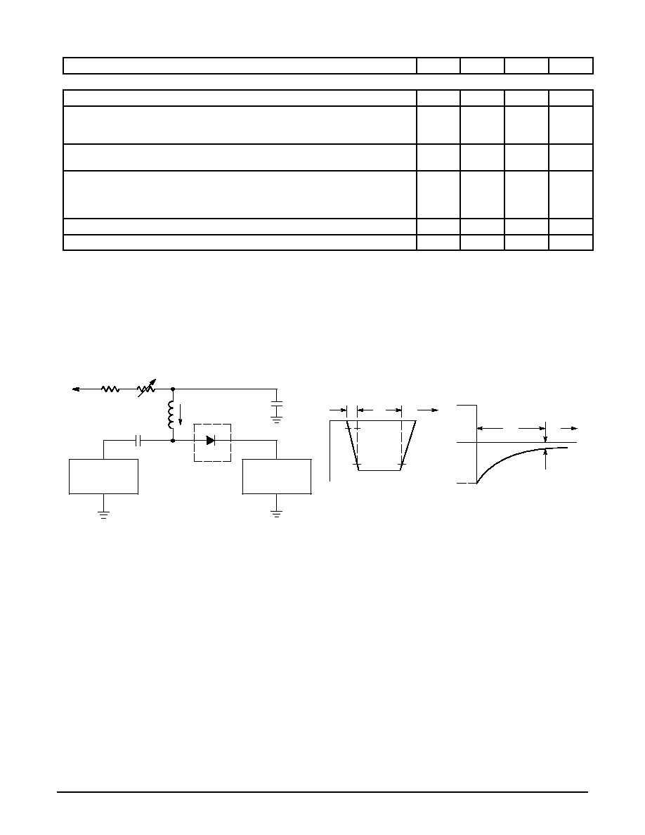
Reverse Recovery Time (IF = IR = 10 mAdc, iR(REC) = 1.0 mAdc) (Figure 1) RL = 100
W
trr
--
6.0
ns
Forward Recovery Voltage (IF = 10 mA, tr = 20 ns)
VFR
--
1.75
V
Notes: 1. A 2.0 k
variable resistor adjusted for a Forward Current (IF) of 10 mA.
Notes:
2. Input pulse is adjusted so IR(peak) is equal to 10 mA.
Notes:
3. tp ª trr
+10 V
2 k
820
0.1
µ
F
DUT
VR
100
µ
H
0.1
µ
F
50
OUTPUT
PULSE
GENERATOR
50
INPUT
SAMPLING
OSCILLOSCOPE
tr
tp
t
10%
90%
IF
IR
trr
t
iR(REC) = 1 mA
OUTPUT PULSE
(IF = IR = 10 mA; measured
at iR(REC) = 1 mA)
IF
INPUT SIGNAL
Figure 1. Recovery Time Equivalent Test Circuit

BAV99WT1 BAV99RWT1
3
Motorola Small≠Signal Transistors, FETs and Diodes Device Data
CURVES APPLICABLE TO EACH DIODE
I R
, REVERSE CURRENT
(
A)
µ
100
0.2
0.4
VF, FORWARD VOLTAGE (VOLTS)
0.6
0.8
1.0
1.2
10
1.0
0.1
TA = 85
∞
C
10
0
VR, REVERSE VOLTAGE (VOLTS)
1.0
0.1
0.01
0.001
10
20
30
40
50
0.68
0
VR, REVERSE VOLTAGE (VOLTS)
0.64
0.60
0.56
0.52
C
D
, DIODE CAP
ACIT
ANCE (pF)
2
4
6
8
I F
, FOR
W
ARD CURRENT
(mA)
TA = 25
∞
C
TA = ≠ 40
∞
C
TA = 150
∞
C
TA = 125
∞
C
TA = 85
∞
C
TA = 55
∞
C
TA = 25
∞
C
Figure 2. Forward Voltage
Figure 3. Leakage Current
Figure 4. Capacitance

BAV99WT1 BAV99RWT1
4
Motorola Small≠Signal Transistors, FETs and Diodes Device Data
INFORMATION FOR USING THE SC≠70/SOT≠323 SURFACE MOUNT PACKAGE
MINIMUM RECOMMENDED FOOTPRINT FOR SURFACE MOUNTED APPLICATIONS
Surface mount board layout is a critical portion of the total
design. The footprint for the semiconductor packages must
be the correct size to insure proper solder connection
interface between the board and the package. With the
correct pad geometry, the packages will self align when
subjected to a solder reflow process.
mm
inches
0.035
0.9
0.075
0.7
1.9
0.028
0.65
0.025
0.65
0.025
SC≠70/SOT≠323
SC≠70/SOT≠323 POWER DISSIPATION
The power dissipation of the SC≠70/SOT≠323 is a function
of the pad size. This can vary from the minimum pad size for
soldering to a pad size given for maximum power dissipation.
Power dissipation for a surface mount device is determined
by TJ(max), the maximum rated junction temperature of the
die, R
JA, the thermal resistance from the device junction to
ambient, and the operating temperature, TA. Using the
values provided on the data sheet for the SC≠70/SOT≠323
package, PD can be calculated as follows:
PD =
TJ(max) ≠ TA
R
JA
The values for the equation are found in the maximum
ratings table on the data sheet. Substituting these values into
the equation for an ambient temperature TA of 25
∞
C, one can
calculate the power dissipation of the device which in this
case is 200 milliwatts.
PD =
150
∞
C ≠ 25
∞
C
625
∞
C/W
= 200 milliwatts
The 625
∞
C/W for the SC≠70/SOT≠323 package assumes
the use of the recommended footprint on a glass epoxy
printed circuit board to achieve a power dissipation of 200
milliwatts. There are other alternatives to achieving higher
power dissipation from the SC≠70/SOT≠323 package.
Another alternative would be to use a ceramic substrate or an
aluminum core board such as Thermal Clad
TM
. Using a board
material such as Thermal Clad, an aluminum core board, the
power dissipation can be doubled using the same footprint.
SOLDERING PRECAUTIONS
The melting temperature of solder is higher than the rated
temperature of the device. When the entire device is heated
to a high temperature, failure to complete soldering within a
short time could result in device failure. Therefore, the
following items should always be observed in order to
minimize the thermal stress to which the devices are
subjected.
∑
Always preheat the device.
∑
The delta temperature between the preheat and soldering
should be 100
∞
C or less.*
∑
When preheating and soldering, the temperature of the
leads and the case must not exceed the maximum
temperature ratings as shown on the data sheet. When
using infrared heating with the reflow soldering method,
the difference shall be a maximum of 10
∞
C.
∑
The soldering temperature and time shall not exceed
260
∞
C for more than 10 seconds.
∑
When shifting from preheating to soldering, the maximum
temperature gradient shall be 5
∞
C or less.
∑
After soldering has been completed, the device should be
allowed to cool naturally for at least three minutes.
Gradual cooling should be used as the use of forced
cooling will increase the temperature gradient and result
in latent failure due to mechanical stress.
∑
Mechanical stress or shock should not be applied during
cooling.
* Soldering a device without preheating can cause excessive
thermal shock and stress which can result in damage to the
device.

BAV99WT1 BAV99RWT1
5
Motorola Small≠Signal Transistors, FETs and Diodes Device Data
PACKAGE DIMENSIONS
CASE 419≠02
ISSUE H
SC≠70/SOT≠323
C
R
N
A
L
D
G
V
S
B
H
J
K
3
1
2
NOTES:
1. DIMENSIONING AND TOLERANCING PER ANSI
Y14.5M, 1982.
2. CONTROLLING DIMENSION: INCH.
DIM
MIN
MAX
MIN
MAX
MILLIMETERS
INCHES
A
0.071
0.087
1.80
2.20
B
0.045
0.053
1.15
1.35
C
0.035
0.049
0.90
1.25
D
0.012
0.016
0.30
0.40
G
0.047
0.055
1.20
1.40
H
0.000
0.004
0.00
0.10
J
0.004
0.010
0.10
0.25
K
0.017 REF
0.425 REF
L
0.026 BSC
0.650 BSC
N
0.028 REF
0.700 REF
R
0.031
0.039
0.80
1.00
S
0.079
0.087
2.00
2.20
V
0.012
0.016
0.30
0.40
0.05 (0.002)
STYLE 9:
PIN 1. ANODE
2. CATHODE
3. CATHODE≠ANODE
STYLE 10:
PIN 1. CATHODE
2. ANODE
3. ANODE≠CATHODE