 | –≠–ª–µ–∫—Ç—Ä–æ–Ω–Ω—ã–π –∫–æ–º–ø–æ–Ω–µ–Ω—Ç: BC847AWT1 | –°–∫–∞—á–∞—Ç—å:  PDF PDF  ZIP ZIP |
1
Motorola Small≠Signal Transistors, FETs and Diodes Device Data
General Purpose Transistors
NPN Silicon
These transistors are designed for general purpose amplifier
applications. They are housed in the SOT≠323/SC≠70 which is
designed for low power surface mount applications.
MAXIMUM RATINGS
Rating
Symbol
BC846
BC847
BC848
Unit
Collector ≠ Emitter Voltage
VCEO
65
45
30
V
Collector ≠ Base Voltage
VCBO
80
50
30
V
Emitter ≠ Base Voltage
VEBO
6.0
6.0
5.0
V
Collector Current -- Continuous
IC
100
100
100
mAdc
THERMAL CHARACTERISTICS
Characteristic
Symbol
Max
Unit
Total Device Dissipation FR≠ 5 Board, (1)
TA = 25
∞
C
PD
150
mW
Thermal Resistance, Junction to Ambient
R
q
JA
833
∞
C/W
Total Device Dissipation
PD
2.4
mW/
∞
C
Junction and Storage Temperature
TJ, Tstg
≠ 55 to +150
∞
C
DEVICE MARKING
BC846AWT1 = 1A; BC846BWT1 = 1B; BC847AWT1 = 1E; BC847BWT1 = 1F;
BC847CWT1 = 1G; BC848AWT1 = 1J; BC848BWT1 = 1K; BC848CWT1 = 1L
ELECTRICAL CHARACTERISTICS
(TA = 25
∞
C unless otherwise noted)
Characteristic
Symbol
Min
Typ
Max
Unit
OFF CHARACTERISTICS
Collector ≠ Emitter Breakdown Voltage
BC846 Series
(IC = 10 mA)
BC847 Series
BC848 Series
V(BR)CEO
65
45
30
--
--
--
--
--
--
V
Collector ≠ Emitter Breakdown Voltage
BC846 Series
(IC = 10
µ
A, VEB = 0)
BC847 Series
BC848 Series
V(BR)CES
80
50
30
--
--
--
--
--
--
V
Collector ≠ Base Breakdown Voltage
BC846 Series
(IC = 10
m
A)
BC847 Series
BC848 Series
V(BR)CBO
80
50
30
--
--
--
--
--
--
V
Emitter ≠ Base Breakdown Voltage
BC846 Series
(IE = 1.0
m
A)
BC847 Series
BC848 Series
V(BR)EBO
6.0
6.0
5.0
--
--
--
--
--
--
V
Collector Cutoff Current (VCB = 30 V)
(VCB = 30 V, TA = 150
∞
C)
ICBO
--
--
--
--
15
5.0
nA
µ
A
1. FR≠5 = 1.0 x 0.75 x 0.062 in
Thermal Clad is a trademark of the Bergquist Company.
Order this document
by BC846AWT1/D
MOTOROLA
SEMICONDUCTOR TECHNICAL DATA
BC846AWT1,BWT1
BC847AWT1,BWT1,
CWT1
BC848AWT1,BWT1,
CWT1
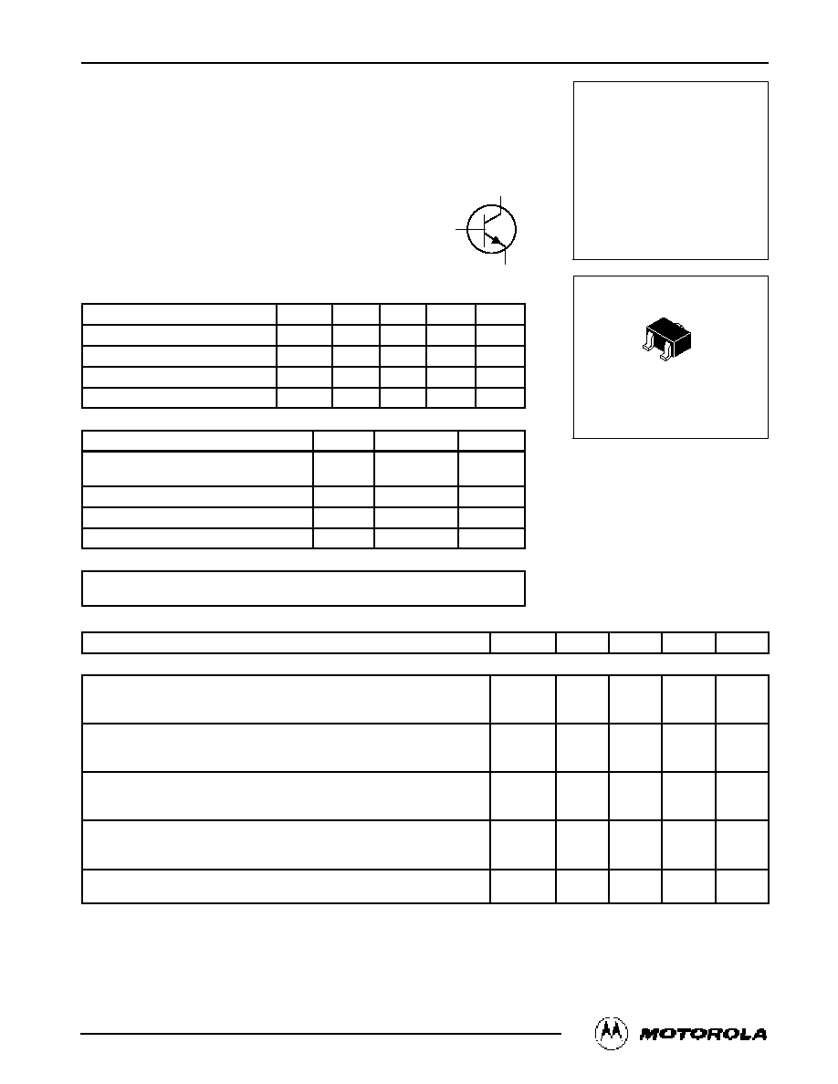
CASE 419≠02, STYLE 3
SOT≠323/SC≠70
1
2
3
©
Motorola, Inc. 1996
COLLECTOR
3
1
BASE
2
EMITTER
BC846AWT1,BWT1 BC847AWT1,BWT1,CWT1 BC848AWT1,BWT1,CWT1
2
Motorola Small≠Signal Transistors, FETs and Diodes Device Data
ELECTRICAL CHARACTERISTICS
(TA = 25
∞
C unless otherwise noted) (Continued)
Characteristic
Symbol
Min
Typ
Max
Unit
ON CHARACTERISTICS
DC Current Gain
BC846A, BC847A, BC848A
(IC = 10
µ
A, VCE = 5.0 V)
BC846B, BC847B, BC848B
BC847C, BC848C
(IC = 2.0 mA, VCE = 5.0 V)
BC846A, BC847A, BC848A
BC846B, BC847B, BC848B
BC847C, BC848C
hFE
--
--
--
110
200
420
90
150
270
180
290
520
--
--
--
220
450
800
--
Collector ≠ Emitter Saturation Voltage (IC = 10 mA, IB = 0.5 mA)
Collector ≠ Emitter Saturation Voltage
(IC = 100 mA, IB = 5.0 mA)
VCE(sat)
--
--
--
--
0.25
0.6
V
Base ≠ Emitter Saturation Voltage (IC = 10 mA, IB = 0.5 mA)
Base ≠ Emitter Saturation Voltage
(IC = 100 mA, IB = 5.0 mA)
VBE(sat)
--
--
0.7
0.9
--
--
V
Base ≠ Emitter Voltage (IC = 2.0 mA, VCE = 5.0 V)
Base ≠ Emitter Voltage
(IC = 10 mA, VCE = 5.0 V)
VBE(on)
580
--
660
--
700
770
mV
SMALL≠ SIGNAL CHARACTERISTICS
Current ≠ Gain -- Bandwidth Product
(IC = 10 mA, VCE = 5.0 Vdc, f = 100 MHz)
fT
100
--
--
MHz
Output Capacitance (VCB = 10 V, f = 1.0 MHz)
Cobo
--
--
4.5
pF
Noise Figure (IC = 0.2 mA,
BC846A, BC847A, BC848A
VCE = 5.0 Vdc, RS = 2.0 k
,
BC846B, BC847B, BC848B
f = 1.0 kHz, BW = 200 Hz)
BC847C, BC848C
NF
--
--
--
--
10
4.0
dB
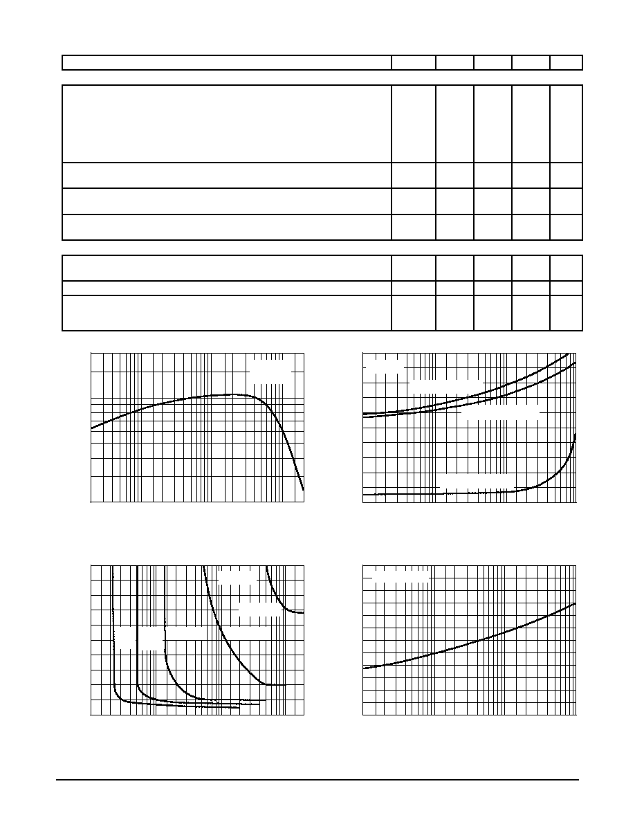
Figure 1. Normalized DC Current Gain
IC, COLLECTOR CURRENT (mAdc)
2.0
Figure 2. "Saturation" and "On" Voltages
IC, COLLECTOR CURRENT (mAdc)
0.2
0.5
1.0
10
20
50
0.2
100
Figure 3. Collector Saturation Region
IB, BASE CURRENT (mA)
Figure 4. Base≠Emitter Temperature Coefficient
IC, COLLECTOR CURRENT (mA)
2.0
5.0
200
0.6
0.7
0.8
0.9
1.0
0.5
0
0.2
0.4
0.1
0.3
1.6
1.2
2.0
2.8
2.4
1.2
1.6
2.0
0.02
1.0
10
0
20
0.1
0.4
0.8
h
FE
, NORMALIZED DC CURRENT
GAIN
V
, VOL
T
AGE (VOL
TS)
V
CE
, COLLECT
OR≠EMITTER VOL
T
AGE (V)
VB
,
TEMPERA
TURE COEFFICIENT
(mV/
C)
∞
1.5
1.0
0.8
0.6
0.4
0.3
0.2
0.5
1.0
10
20
50
2.0
100
70
30
7.0
5.0
3.0
0.7
0.3
0.1
0.2
1.0
10
100
TA = 25
∞
C
VBE(sat) @ IC/IB = 10
VCE(sat) @ IC/IB = 10
VBE(on) @ VCE = 10 V
VCE = 10 V
TA = 25
∞
C
≠55
∞
C to +125
∞
C
TA = 25
∞
C
IC = 50 mA
IC = 100 mA
IC = 200 mA
IC =
20 mA
IC =
10 mA
1.0
BC846AWT1,BWT1 BC847AWT1,BWT1,CWT1 BC848AWT1,BWT1,CWT1
3
Motorola Small≠Signal Transistors, FETs and Diodes Device Data
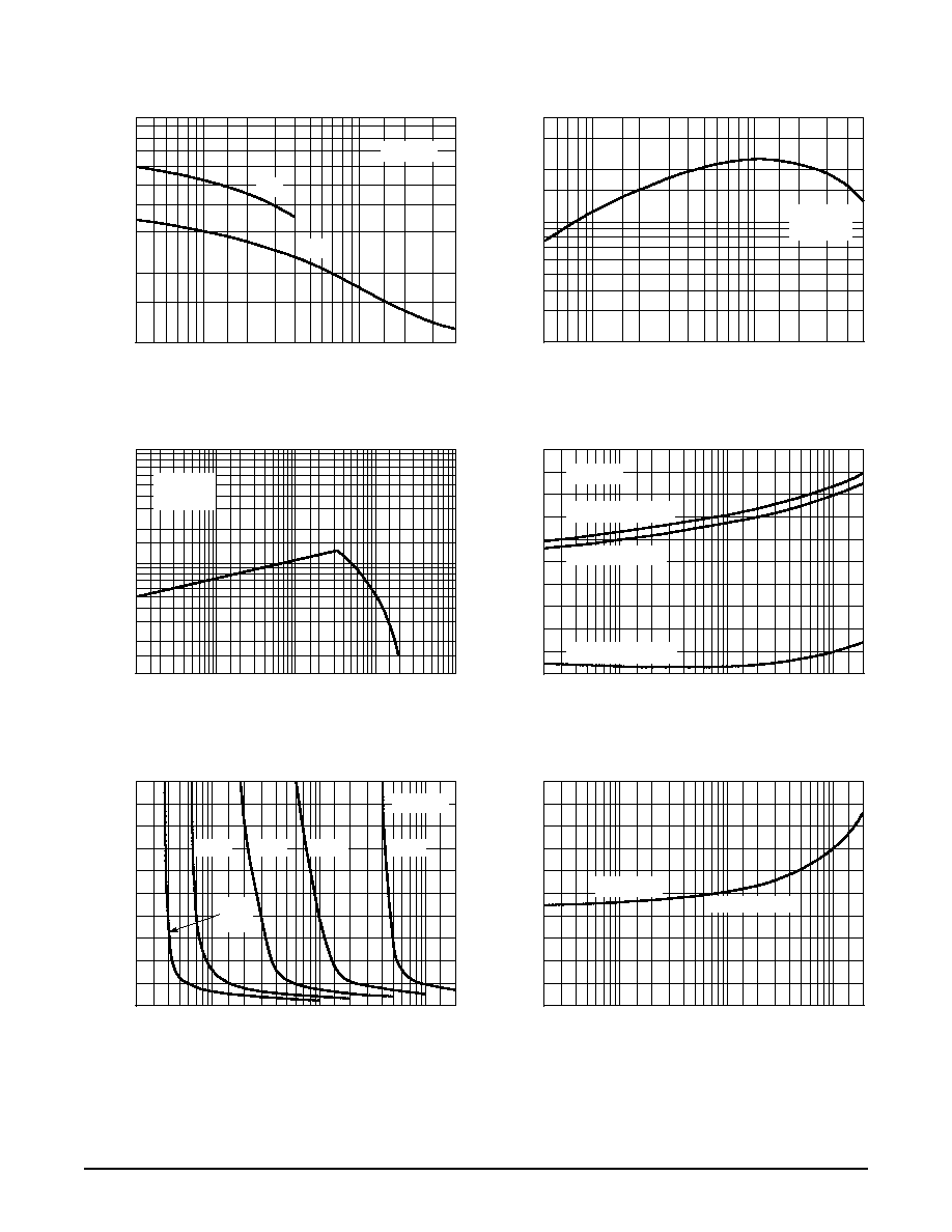
BC847/BC848
Figure 5. Capacitances
VR, REVERSE VOLTAGE (VOLTS)
10
Figure 6. Current≠Gain ≠ Bandwidth Product
IC, COLLECTOR CURRENT (mAdc)
0.4
0.6
1.0
10
20
1.0
Figure 7. DC Current Gain
IC, COLLECTOR CURRENT (mA)
Figure 8. "On" Voltage
IC, COLLECTOR CURRENT (mA)
2.0
6.0
40
80
100
200
300
400
60
20
40
30
0.8
1.0
0.6
0.2
0.4
1.0
2.0
0.1
1.0
10
100
0.2
0.2
0.5
7.0
5.0
3.0
2.0
0.7
1.0
10
20
2.0
50
30
7.0
5.0
3.0
0.5
0.2
1.0
10
200
TA = 25
∞
C
VBE(sat) @ IC/IB = 10
VCE(sat) @ IC/IB = 10
VBE @ VCE = 5.0 V
VCE = 10 V
TA = 25
∞
C
Figure 9. Collector Saturation Region
IB, BASE CURRENT (mA)
Figure 10. Base≠Emitter Temperature Coefficient
IC, COLLECTOR CURRENT (mA)
≠1.0
1.2
1.6
2.0
0.02
1.0
10
0
20
0.1
0.4
0.8
V
CE
, COLLECT
OR≠EMITTER VOL
T
AGE (VOL
TS)
VB
,
TEMPERA
TURE COEFFICIENT
(mV/
C)
∞
0.2
2.0
10
200
1.0
TA = 25
∞
C
200 mA
50 mA
IC =
10 mA
h
FE
, DC CURRENT
GAIN (NORMALIZED)
V
, VOL
T
AGE (VOL
TS)
C, CAP
ACIT
ANCE (pF)
f
, CURRENT≠GAIN ≠ BANDWIDTH PRODUCT
(MHz)
T
0.8
4.0
8.0
TA = 25
∞
C
Cob
Cib
VCE = 5 V
TA = 25
∞
C
0
0.5
2.0
5.0
20
50
100
0.05
0.2
0.5
2.0
5.0
100 mA
20 mA
≠1.4
≠1.8
≠2.2
≠2.6
≠3.0
0.5
5.0
20
50
100
≠55
∞
C to 125
∞
C
VB for VBE
BC846AWT1,BWT1 BC847AWT1,BWT1,CWT1 BC848AWT1,BWT1,CWT1
4
Motorola Small≠Signal Transistors, FETs and Diodes Device Data
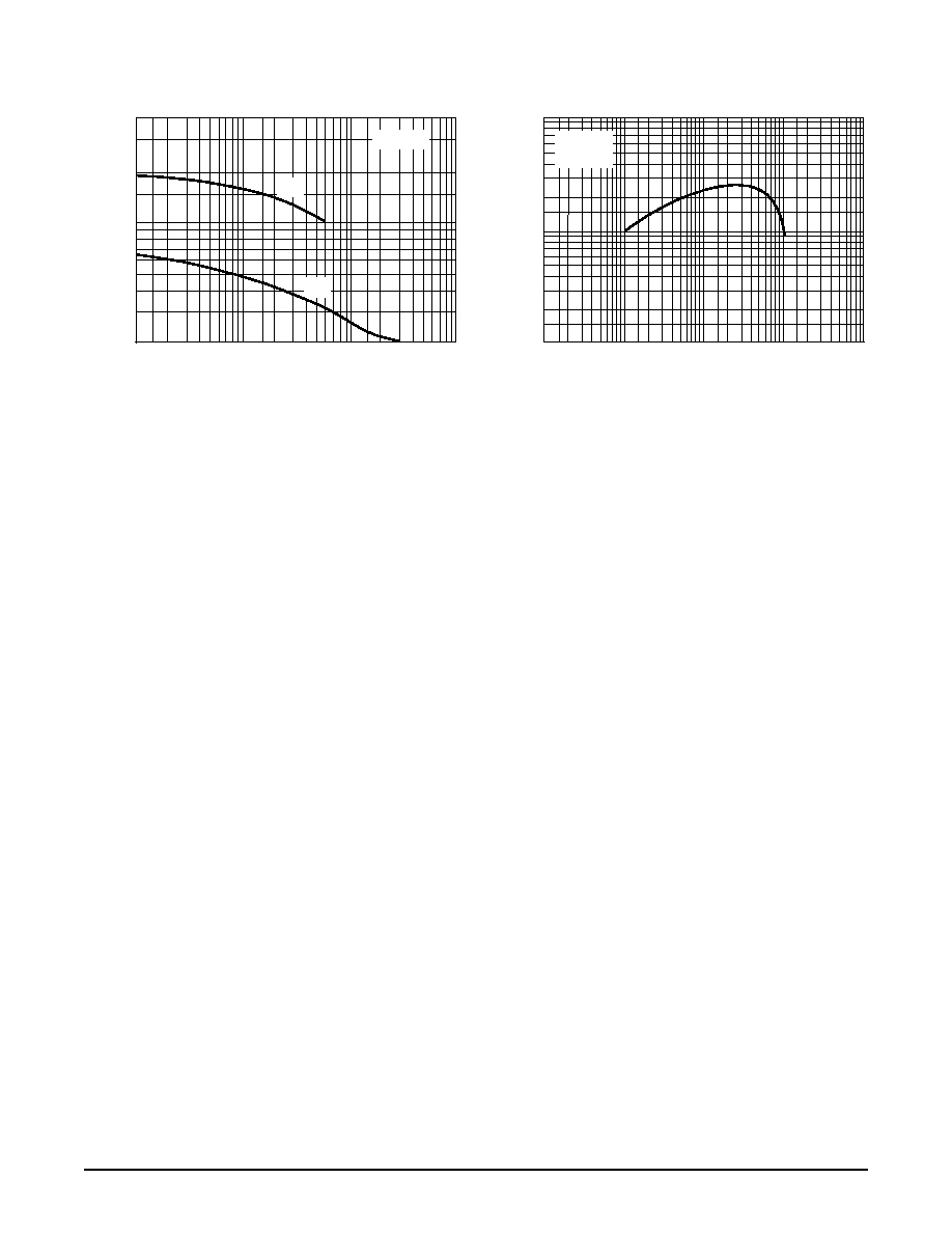
BC846
Figure 11. Capacitance
VR, REVERSE VOLTAGE (VOLTS)
40
Figure 12. Current≠Gain ≠ Bandwidth Product
IC, COLLECTOR CURRENT (mA)
0.1
0.2
1.0
50
2.0
2.0
10
100
100
200
500
50
20
20
10
6.0
4.0
1.0
10
50 100
5.0
VCE = 5 V
TA = 25
∞
C
C, CAP
ACIT
ANCE (pF)
f
, CURRENT≠GAIN ≠ BANDWIDTH PRODUCT T
0.5
5.0
20
TA = 25
∞
C
Cob
Cib
BC846AWT1,BWT1 BC847AWT1,BWT1,CWT1 BC848AWT1,BWT1,CWT1
5
Motorola Small≠Signal Transistors, FETs and Diodes Device Data
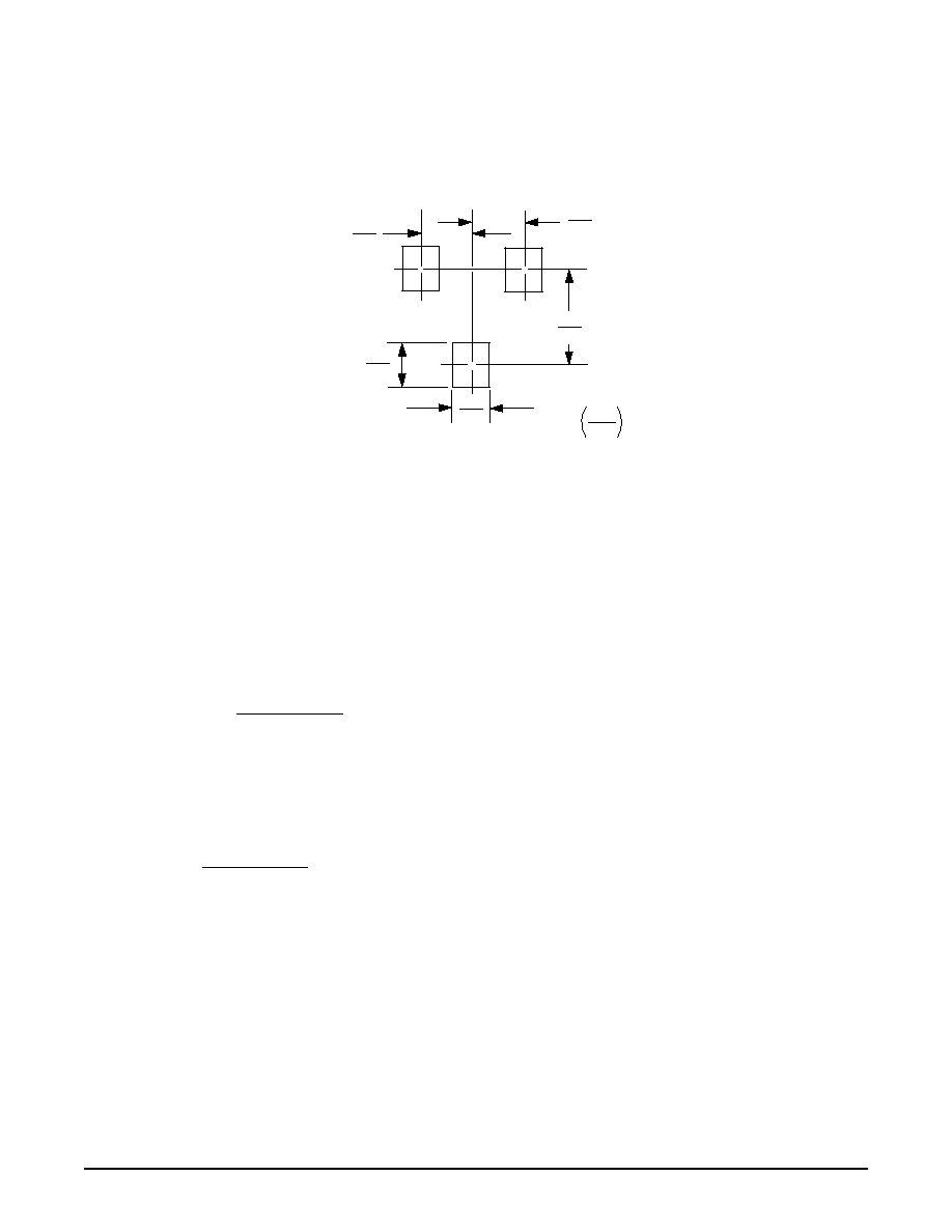
INFORMATION FOR USING THE SOT≠323/SC≠70 SURFACE MOUNT PACKAGE
MINIMUM RECOMMENDED FOOTPRINT FOR SURFACE MOUNTED APPLICATIONS
Surface mount board layout is a critical portion of the total
design. The footprint for the semiconductor packages must
be the correct size to insure proper solder connection
interface between the board and the package. With the
correct pad geometry, the packages will self align when
subjected to a solder reflow process.
SOT≠323/SC≠70
mm
inches
0.035
0.9
0.075
0.7
1.9
0.028
0.65
0.025
0.65
0.025
SOT≠323/SC≠70 POWER DISSIPATION
The power dissipation of the SOT≠323/SC≠70 is a function
of the pad size. This can vary from the minimum pad size for
soldering to a pad size given for maximum power dissipation.
Power dissipation for a surface mount device is determined
by TJ(max), the maximum rated junction temperature of the
die, R
JA, the thermal resistance from the device junction to
ambient, and the operating temperature, TA. Using the
values provided on the data sheet for the SOT≠323/SC≠70
package, PD can be calculated as follows:
PD =
TJ(max) ≠ TA
R
JA
The values for the equation are found in the maximum
ratings table on the data sheet. Substituting these values into
the equation for an ambient temperature TA of 25
∞
C, one can
calculate the power dissipation of the device which in this
case is 150 milliwatts.
PD =
150
∞
C ≠ 25
∞
C
833
∞
C/W
= 150 milliwatts
The 833
∞
C/W for the SOT≠323/SC≠70 package assumes
the use of the recommended footprint on a glass epoxy
printed circuit board to achieve a power dissipation of
150 milliwatts. There are other alternatives to achieving
higher power dissipation from the SOT≠323/SC≠70
package. Another alternative would be to use a ceramic
substrate or an aluminum core board such as Thermal
Clad
TM
. Using a board material such as Thermal Clad, an
aluminum core board, the power dissipation can be doubled
using the same footprint.
SOLDERING PRECAUTIONS
The melting temperature of solder is higher than the rated
temperature of the device. When the entire device is heated
to a high temperature, failure to complete soldering within a
short time could result in device failure. Therefore, the
following items should always be observed in order to
minimize the thermal stress to which the devices are
subjected.
∑
Always preheat the device.
∑
The delta temperature between the preheat and
soldering should be 100
∞
C or less.*
∑
When preheating and soldering, the temperature of the
leads and the case must not exceed the maximum
temperature ratings as shown on the data sheet. When
using infrared heating with the reflow soldering method,
the difference shall be a maximum of 10
∞
C.
∑
The soldering temperature and time shall not exceed
260
∞
C for more than 10 seconds.
∑
When shifting from preheating to soldering, the
maximum temperature gradient shall be 5
∞
C or less.
∑
After soldering has been completed, the device should
be allowed to cool naturally for at least three minutes.
Gradual cooling should be used as the use of forced
cooling will increase the temperature gradient and result
in latent failure due to mechanical stress.
∑
Mechanical stress or shock should not be applied during
cooling.
* Soldering a device without preheating can cause excessive
thermal shock and stress which can result in damage to the
device.
BC846AWT1,BWT1 BC847AWT1,BWT1,CWT1 BC848AWT1,BWT1,CWT1
6
Motorola Small≠Signal Transistors, FETs and Diodes Device Data
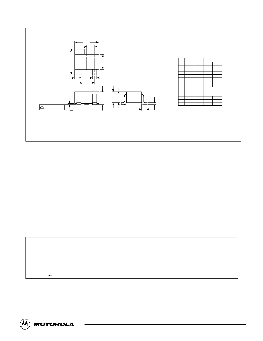
PACKAGE DIMENSIONS
CASE 419≠02
ISSUE G
SOT≠323/SC≠70
STYLE 3:
PIN 1. BASE
2. EMITTER
3. COLLECTOR
C
R
N
A
L
D
G
V
S
B
H
J
K
3
1
2
NOTES:
1. DIMENSIONING AND TOLERANCING PER ANSI
Y14.5M, 1982.
2. CONTROLLING DIMENSION: INCH.
DIM
MIN
MAX
MIN
MAX
MILLIMETERS
INCHES
A
0.071
0.087
1.80
2.20
B
0.045
0.053
1.15
1.35
C
0.035
0.049
0.90
1.25
D
0.012
0.016
0.30
0.40
G
0.047
0.055
1.20
1.40
H
0.000
0.004
0.00
0.10
J
0.004
0.010
0.10
0.25
K
0.017 REF
0.425 REF
L
0.026 BSC
0.650 BSC
N
0.028 REF
0.700 REF
R
0.031
0.039
0.80
1.00
S
0.079
0.087
2.00
2.20
V
0.012
0.016
0.30
0.40
0.05 (0.002)
Motorola reserves the right to make changes without further notice to any products herein. Motorola makes no warranty, representation or guarantee regarding
the suitability of its products for any particular purpose, nor does Motorola assume any liability arising out of the application or use of any product or circuit,
and specifically disclaims any and all liability, including without limitation consequential or incidental damages. "Typical" parameters can and do vary in different
applications. All operating parameters, including "Typicals" must be validated for each customer application by customer's technical experts. Motorola does
not convey any license under its patent rights nor the rights of others. Motorola products are not designed, intended, or authorized for use as components in
systems intended for surgical implant into the body, or other applications intended to support or sustain life, or for any other application in which the failure of
the Motorola product could create a situation where personal injury or death may occur. Should Buyer purchase or use Motorola products for any such
unintended or unauthorized application, Buyer shall indemnify and hold Motorola and its officers, employees, subsidiaries, affiliates, and distributors harmless
against all claims, costs, damages, and expenses, and reasonable attorney fees arising out of, directly or indirectly, any claim of personal injury or death
associated with such unintended or unauthorized use, even if such claim alleges that Motorola was negligent regarding the design or manufacture of the part.
Motorola and
are registered trademarks of Motorola, Inc. Motorola, Inc. is an Equal Opportunity/Affirmative Action Employer.
How to reach us:
USA/EUROPE: Motorola Literature Distribution;
JAPAN: Nippon Motorola Ltd.; Tatsumi≠SPD≠JLDC, Toshikatsu Otsuki,
P.O. Box 20912; Phoenix, Arizona 85036. 1≠800≠441≠2447
6F Seibu≠Butsuryu≠Center, 3≠14≠2 Tatsumi Koto≠Ku, Tokyo 135, Japan. 03≠3521≠8315
MFAX: RMFAX0@email.sps.mot.com ≠ TOUCHTONE (602) 244≠6609
HONG KONG: Motorola Semiconductors H.K. Ltd.; 8B Tai Ping Industrial Park,
INTERNET: http://Design≠NET.com
51 Ting Kok Road, Tai Po, N.T., Hong Kong. 852≠26629298
BC846AWT1/D
*BC846AWT1/D*