3≠1
Motorola Bipolar Power Transistor Device Data
NPN Silicon Darlington Power
Transistor
The BU323AP is a monolithic darlington transistor designed for automotive ignition,
switching regulator and motor control applications.
∑
Collector≠Emitter Sustaining Voltage --
VCER(sus) = 475 Vdc
∑
125 Watts Capability at 50 Volts
∑
VCE Sat Specified at ≠40
_
C = 2.0 V Max. at IC = 6.0 A
∑
Photoglass Passivation for Reliability and Stability
ŒŒŒŒŒŒŒŒŒŒŒŒŒŒŒŒŒŒŒŒŒŒŒŒŒŒŒŒŒŒŒŒŒŒ
ŒŒŒŒŒŒŒŒŒŒŒŒŒŒŒŒŒŒŒŒŒŒŒŒŒŒŒŒŒŒŒŒŒŒ
ŒŒŒŒŒŒŒŒŒŒŒŒŒŒŒŒŒŒŒŒŒŒŒŒŒŒŒŒŒŒŒŒŒŒ
ŒŒŒŒŒŒŒŒŒŒŒŒŒŒŒŒŒŒŒŒŒŒŒŒŒŒŒŒŒŒŒŒŒŒ
MAXIMUM RATINGS
ŒŒŒŒŒŒŒŒŒŒŒŒŒŒŒŒŒŒ
ŒŒŒŒŒŒŒŒŒŒŒŒŒŒŒŒŒŒ
ŒŒŒŒŒŒŒŒŒŒŒŒŒŒŒŒŒŒ
ŒŒŒŒŒŒŒŒŒŒŒŒŒŒŒŒŒŒ
Rating
ŒŒŒŒŒŒŒ
ŒŒŒŒŒŒŒ
ŒŒŒŒŒŒŒ
ŒŒŒŒŒŒŒ
Symbol
ŒŒŒŒŒŒŒŒ
ŒŒŒŒŒŒŒŒ
ŒŒŒŒŒŒŒŒ
ŒŒŒŒŒŒŒŒ
Value
ŒŒŒŒ
ŒŒŒŒ
ŒŒŒŒ
ŒŒŒŒ
Unit
ŒŒŒŒŒŒŒŒŒŒŒŒŒŒŒŒŒŒ
ŒŒŒŒŒŒŒŒŒŒŒŒŒŒŒŒŒŒ
ŒŒŒŒŒŒŒŒŒŒŒŒŒŒŒŒŒŒ
ŒŒŒŒŒŒŒŒŒŒŒŒŒŒŒŒŒŒ
Collector≠Emitter Voltage
ŒŒŒŒŒŒŒ
ŒŒŒŒŒŒŒ
ŒŒŒŒŒŒŒ
ŒŒŒŒŒŒŒ
VCEO(sus)
ŒŒŒŒŒŒŒŒ
ŒŒŒŒŒŒŒŒ
ŒŒŒŒŒŒŒŒ
ŒŒŒŒŒŒŒŒ
400
ŒŒŒŒ
ŒŒŒŒ
ŒŒŒŒ
ŒŒŒŒ
Vdc
ŒŒŒŒŒŒŒŒŒŒŒŒŒŒŒŒŒŒ
ŒŒŒŒŒŒŒŒŒŒŒŒŒŒŒŒŒŒ
ŒŒŒŒŒŒŒŒŒŒŒŒŒŒŒŒŒŒ
ŒŒŒŒŒŒŒŒŒŒŒŒŒŒŒŒŒŒ
Collector≠Emitter Voltage
ŒŒŒŒŒŒŒ
ŒŒŒŒŒŒŒ
ŒŒŒŒŒŒŒ
ŒŒŒŒŒŒŒ
VCEV
ŒŒŒŒŒŒŒŒ
ŒŒŒŒŒŒŒŒ
ŒŒŒŒŒŒŒŒ
ŒŒŒŒŒŒŒŒ
475
ŒŒŒŒ
ŒŒŒŒ
ŒŒŒŒ
ŒŒŒŒ
Vdc
ŒŒŒŒŒŒŒŒŒŒŒŒŒŒŒŒŒŒ
ŒŒŒŒŒŒŒŒŒŒŒŒŒŒŒŒŒŒ
ŒŒŒŒŒŒŒŒŒŒŒŒŒŒŒŒŒŒ
ŒŒŒŒŒŒŒŒŒŒŒŒŒŒŒŒŒŒ
Emitter≠Base Voltage
ŒŒŒŒŒŒŒ
ŒŒŒŒŒŒŒ
ŒŒŒŒŒŒŒ
ŒŒŒŒŒŒŒ
VEB
ŒŒŒŒŒŒŒŒ
ŒŒŒŒŒŒŒŒ
ŒŒŒŒŒŒŒŒ
ŒŒŒŒŒŒŒŒ
6.0
ŒŒŒŒ
ŒŒŒŒ
ŒŒŒŒ
ŒŒŒŒ
Vdc
ŒŒŒŒŒŒŒŒŒŒŒŒŒŒŒŒŒŒ
ŒŒŒŒŒŒŒŒŒŒŒŒŒŒŒŒŒŒ
ŒŒŒŒŒŒŒŒŒŒŒŒŒŒŒŒŒŒ
ŒŒŒŒŒŒŒŒŒŒŒŒŒŒŒŒŒŒ
ŒŒŒŒŒŒŒŒŒŒŒŒŒŒŒŒŒŒ
Collector Current -- Continuous
-- Peak (1)
ŒŒŒŒŒŒŒ
ŒŒŒŒŒŒŒ
ŒŒŒŒŒŒŒ
ŒŒŒŒŒŒŒ
ŒŒŒŒŒŒŒ
IC
ICM
ŒŒŒŒŒŒŒŒ
ŒŒŒŒŒŒŒŒ
ŒŒŒŒŒŒŒŒ
ŒŒŒŒŒŒŒŒ
ŒŒŒŒŒŒŒŒ
10
16
ŒŒŒŒ
ŒŒŒŒ
ŒŒŒŒ
ŒŒŒŒ
ŒŒŒŒ
Adc
ŒŒŒŒŒŒŒŒŒŒŒŒŒŒŒŒŒŒ
ŒŒŒŒŒŒŒŒŒŒŒŒŒŒŒŒŒŒ
ŒŒŒŒŒŒŒŒŒŒŒŒŒŒŒŒŒŒ
ŒŒŒŒŒŒŒŒŒŒŒŒŒŒŒŒŒŒ
ŒŒŒŒŒŒŒŒŒŒŒŒŒŒŒŒŒŒ
Base Current -- Continuous
-- Peak (1)
ŒŒŒŒŒŒŒ
ŒŒŒŒŒŒŒ
ŒŒŒŒŒŒŒ
ŒŒŒŒŒŒŒ
ŒŒŒŒŒŒŒ
IB
IBM
ŒŒŒŒŒŒŒŒ
ŒŒŒŒŒŒŒŒ
ŒŒŒŒŒŒŒŒ
ŒŒŒŒŒŒŒŒ
ŒŒŒŒŒŒŒŒ
3.0
ŒŒŒŒ
ŒŒŒŒ
ŒŒŒŒ
ŒŒŒŒ
ŒŒŒŒ
Adc
ŒŒŒŒŒŒŒŒŒŒŒŒŒŒŒŒŒŒ
ŒŒŒŒŒŒŒŒŒŒŒŒŒŒŒŒŒŒ
ŒŒŒŒŒŒŒŒŒŒŒŒŒŒŒŒŒŒ
ŒŒŒŒŒŒŒŒŒŒŒŒŒŒŒŒŒŒ
ŒŒŒŒŒŒŒŒŒŒŒŒŒŒŒŒŒŒ
Total Power Dissipation -- TC = 25
_
C
-- TC = 100
_
C
Derate above 25
_
C
ŒŒŒŒŒŒŒ
ŒŒŒŒŒŒŒ
ŒŒŒŒŒŒŒ
ŒŒŒŒŒŒŒ
ŒŒŒŒŒŒŒ
PD
ŒŒŒŒŒŒŒŒ
ŒŒŒŒŒŒŒŒ
ŒŒŒŒŒŒŒŒ
ŒŒŒŒŒŒŒŒ
ŒŒŒŒŒŒŒŒ
125
100
1.0
ŒŒŒŒ
ŒŒŒŒ
ŒŒŒŒ
ŒŒŒŒ
ŒŒŒŒ
Watts
Watts
W/
_
C
ŒŒŒŒŒŒŒŒŒŒŒŒŒŒŒŒŒŒ
ŒŒŒŒŒŒŒŒŒŒŒŒŒŒŒŒŒŒ
ŒŒŒŒŒŒŒŒŒŒŒŒŒŒŒŒŒŒ
ŒŒŒŒŒŒŒŒŒŒŒŒŒŒŒŒŒŒ
Operating and Storage Junction Temperature Range
ŒŒŒŒŒŒŒ
ŒŒŒŒŒŒŒ
ŒŒŒŒŒŒŒ
ŒŒŒŒŒŒŒ
TJ, Tstg
ŒŒŒŒŒŒŒŒ
ŒŒŒŒŒŒŒŒ
ŒŒŒŒŒŒŒŒ
ŒŒŒŒŒŒŒŒ
≠ 65 to + 200
ŒŒŒŒ
ŒŒŒŒ
ŒŒŒŒ
ŒŒŒŒ
_
C
ŒŒŒŒŒŒŒŒŒŒŒŒŒŒŒŒŒŒŒŒŒŒŒŒŒŒŒŒŒŒŒŒŒŒ
ŒŒŒŒŒŒŒŒŒŒŒŒŒŒŒŒŒŒŒŒŒŒŒŒŒŒŒŒŒŒŒŒŒŒ
ŒŒŒŒŒŒŒŒŒŒŒŒŒŒŒŒŒŒŒŒŒŒŒŒŒŒŒŒŒŒŒŒŒŒ
ŒŒŒŒŒŒŒŒŒŒŒŒŒŒŒŒŒŒŒŒŒŒŒŒŒŒŒŒŒŒŒŒŒŒ
THERMAL CHARACTERISTICS
ŒŒŒŒŒŒŒŒŒŒŒŒŒŒŒŒŒŒ
ŒŒŒŒŒŒŒŒŒŒŒŒŒŒŒŒŒŒ
ŒŒŒŒŒŒŒŒŒŒŒŒŒŒŒŒŒŒ
ŒŒŒŒŒŒŒŒŒŒŒŒŒŒŒŒŒŒ
Characteristic
ŒŒŒŒŒŒŒ
ŒŒŒŒŒŒŒ
ŒŒŒŒŒŒŒ
ŒŒŒŒŒŒŒ
Symbol
ŒŒŒŒŒŒŒŒ
ŒŒŒŒŒŒŒŒ
ŒŒŒŒŒŒŒŒ
ŒŒŒŒŒŒŒŒ
Max
ŒŒŒŒ
ŒŒŒŒ
ŒŒŒŒ
ŒŒŒŒ
Unit
ŒŒŒŒŒŒŒŒŒŒŒŒŒŒŒŒŒŒ
ŒŒŒŒŒŒŒŒŒŒŒŒŒŒŒŒŒŒ
ŒŒŒŒŒŒŒŒŒŒŒŒŒŒŒŒŒŒ
ŒŒŒŒŒŒŒŒŒŒŒŒŒŒŒŒŒŒ
Thermal Resistance, Junction to Case
ŒŒŒŒŒŒŒ
ŒŒŒŒŒŒŒ
ŒŒŒŒŒŒŒ
ŒŒŒŒŒŒŒ
R
JC
ŒŒŒŒŒŒŒŒ
ŒŒŒŒŒŒŒŒ
ŒŒŒŒŒŒŒŒ
ŒŒŒŒŒŒŒŒ
1.0
ŒŒŒŒ
ŒŒŒŒ
ŒŒŒŒ
ŒŒŒŒ
_
C/W
ŒŒŒŒŒŒŒŒŒŒŒŒŒŒŒŒŒŒ
ŒŒŒŒŒŒŒŒŒŒŒŒŒŒŒŒŒŒ
ŒŒŒŒŒŒŒŒŒŒŒŒŒŒŒŒŒŒ
ŒŒŒŒŒŒŒŒŒŒŒŒŒŒŒŒŒŒ
ŒŒŒŒŒŒŒŒŒŒŒŒŒŒŒŒŒŒ
Maximum Lead Temperature for Soldering Purposes:
1/8
from Case for 5 Seconds
ŒŒŒŒŒŒŒ
ŒŒŒŒŒŒŒ
ŒŒŒŒŒŒŒ
ŒŒŒŒŒŒŒ
ŒŒŒŒŒŒŒ
TL
ŒŒŒŒŒŒŒŒ
ŒŒŒŒŒŒŒŒ
ŒŒŒŒŒŒŒŒ
ŒŒŒŒŒŒŒŒ
ŒŒŒŒŒŒŒŒ
275
ŒŒŒŒ
ŒŒŒŒ
ŒŒŒŒ
ŒŒŒŒ
ŒŒŒŒ
_
C
(1) Pulse Test: Pulse Width = 5.0 ms, Duty Cycle
x
10%.
MOTOROLA
SEMICONDUCTOR TECHNICAL DATA
Order this document
by BU323AP/D
©
Motorola, Inc. 1995
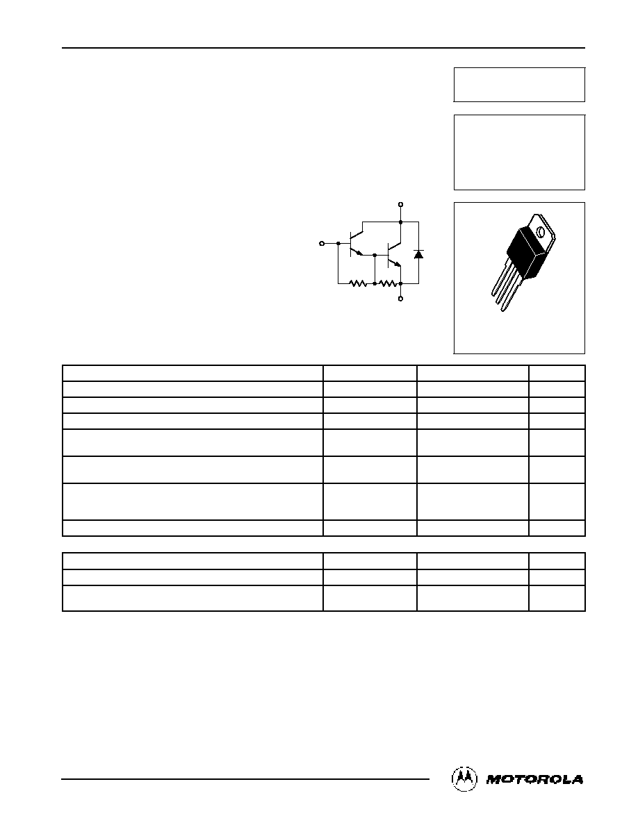
BU323AP
DARLINGTON
NPN SILICON
POWER TRANSISTOR
400 VOLTS
125 WATTS
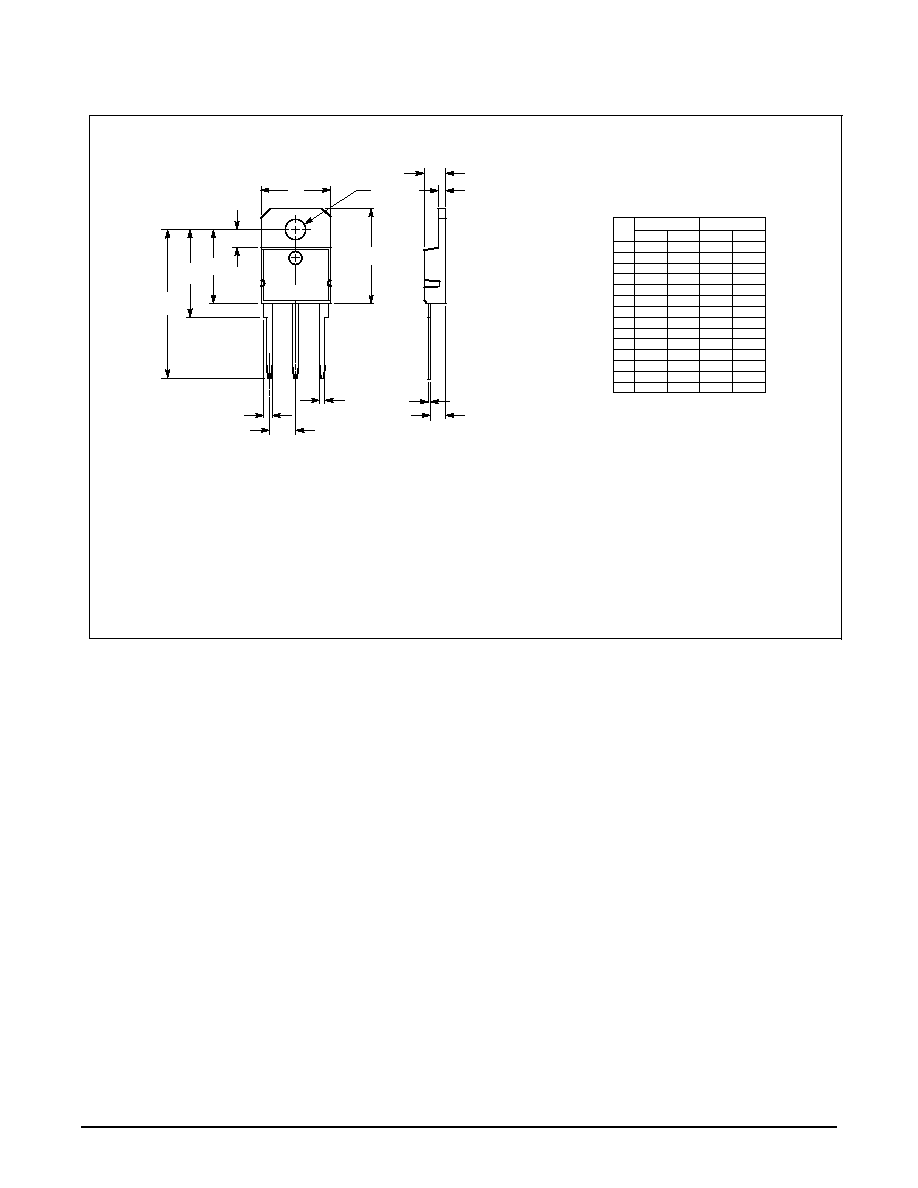
CASE 340D≠01
TO≠218 TYPE
COLLECTOR
EMITTER
BASE
1 k
30
REV 7
BU323AP
3≠2
Motorola Bipolar Power Transistor Device Data
ŒŒŒŒŒŒŒŒŒŒŒŒŒŒŒŒŒŒŒŒŒŒŒŒŒŒŒŒŒŒŒŒŒŒ
ŒŒŒŒŒŒŒŒŒŒŒŒŒŒŒŒŒŒŒŒŒŒŒŒŒŒŒŒŒŒŒŒŒŒ
ŒŒŒŒŒŒŒŒŒŒŒŒŒŒŒŒŒŒŒŒŒŒŒŒŒŒŒŒŒŒŒŒŒŒ
ŒŒŒŒŒŒŒŒŒŒŒŒŒŒŒŒŒŒŒŒŒŒŒŒŒŒŒŒŒŒŒŒŒŒ
ELECTRICAL CHARACTERISTICS
(TC = 25
_
C unless otherwise noted)
ŒŒŒŒŒŒŒŒŒŒŒŒŒŒŒŒŒŒŒŒ
ŒŒŒŒŒŒŒŒŒŒŒŒŒŒŒŒŒŒŒŒ
ŒŒŒŒŒŒŒŒŒŒŒŒŒŒŒŒŒŒŒŒ
ŒŒŒŒŒŒŒŒŒŒŒŒŒŒŒŒŒŒŒŒ
Characteristic
ŒŒŒŒ
ŒŒŒŒ
ŒŒŒŒ
ŒŒŒŒ
Symbol
ŒŒŒŒ
ŒŒŒŒ
ŒŒŒŒ
ŒŒŒŒ
Min
ŒŒŒŒ
ŒŒŒŒ
ŒŒŒŒ
ŒŒŒŒ
Typ
ŒŒŒŒ
ŒŒŒŒ
ŒŒŒŒ
ŒŒŒŒ
Max
ŒŒŒ
ŒŒŒ
ŒŒŒ
ŒŒŒ
Unit
ŒŒŒŒŒŒŒŒŒŒŒŒŒŒŒŒŒŒŒŒŒŒŒŒŒŒŒŒŒŒŒŒŒŒ
ŒŒŒŒŒŒŒŒŒŒŒŒŒŒŒŒŒŒŒŒŒŒŒŒŒŒŒŒŒŒŒŒŒŒ
ŒŒŒŒŒŒŒŒŒŒŒŒŒŒŒŒŒŒŒŒŒŒŒŒŒŒŒŒŒŒŒŒŒŒ
ŒŒŒŒŒŒŒŒŒŒŒŒŒŒŒŒŒŒŒŒŒŒŒŒŒŒŒŒŒŒŒŒŒŒ
OFF CHARACTERISTICS1
ŒŒŒŒŒŒŒŒŒŒŒŒŒŒŒŒŒŒŒŒ
ŒŒŒŒŒŒŒŒŒŒŒŒŒŒŒŒŒŒŒŒ
ŒŒŒŒŒŒŒŒŒŒŒŒŒŒŒŒŒŒŒŒ
ŒŒŒŒŒŒŒŒŒŒŒŒŒŒŒŒŒŒŒŒ
ŒŒŒŒŒŒŒŒŒŒŒŒŒŒŒŒŒŒŒŒ
ŒŒŒŒŒŒŒŒŒŒŒŒŒŒŒŒŒŒŒŒ
Collector≠Emitter Sustaining Voltage (Figure 1)
L = 10 mH
(IC = 200 mAdc, IB = 0, Vclamp = Rated VCEO)
ŒŒŒŒ
ŒŒŒŒ
ŒŒŒŒ
ŒŒŒŒ
ŒŒŒŒ
ŒŒŒŒ
VCEO(sus)
ŒŒŒŒ
ŒŒŒŒ
ŒŒŒŒ
ŒŒŒŒ
ŒŒŒŒ
ŒŒŒŒ
400
ŒŒŒŒ
ŒŒŒŒ
ŒŒŒŒ
ŒŒŒŒ
ŒŒŒŒ
ŒŒŒŒ
ŒŒŒŒ
ŒŒŒŒ
ŒŒŒŒ
ŒŒŒŒ
ŒŒŒŒ
ŒŒŒŒ
ŒŒŒ
ŒŒŒ
ŒŒŒ
ŒŒŒ
ŒŒŒ
ŒŒŒ
Vdc
ŒŒŒŒŒŒŒŒŒŒŒŒŒŒŒŒŒŒŒŒ
ŒŒŒŒŒŒŒŒŒŒŒŒŒŒŒŒŒŒŒŒ
ŒŒŒŒŒŒŒŒŒŒŒŒŒŒŒŒŒŒŒŒ
ŒŒŒŒŒŒŒŒŒŒŒŒŒŒŒŒŒŒŒŒ
ŒŒŒŒŒŒŒŒŒŒŒŒŒŒŒŒŒŒŒŒ
Collector≠Emitter Sustaining Voltage (Figure 1)
(IC = 3 A, RBE = 100 Ohms, L = 500
µ
H)
Unclamped
ŒŒŒŒ
ŒŒŒŒ
ŒŒŒŒ
ŒŒŒŒ
ŒŒŒŒ
VCER(sus)
ŒŒŒŒ
ŒŒŒŒ
ŒŒŒŒ
ŒŒŒŒ
ŒŒŒŒ
475
ŒŒŒŒ
ŒŒŒŒ
ŒŒŒŒ
ŒŒŒŒ
ŒŒŒŒ
ŒŒŒŒ
ŒŒŒŒ
ŒŒŒŒ
ŒŒŒŒ
ŒŒŒŒ
ŒŒŒ
ŒŒŒ
ŒŒŒ
ŒŒŒ
ŒŒŒ
Vdc
ŒŒŒŒŒŒŒŒŒŒŒŒŒŒŒŒŒŒŒŒ
ŒŒŒŒŒŒŒŒŒŒŒŒŒŒŒŒŒŒŒŒ
ŒŒŒŒŒŒŒŒŒŒŒŒŒŒŒŒŒŒŒŒ
ŒŒŒŒŒŒŒŒŒŒŒŒŒŒŒŒŒŒŒŒ
Collector Cutoff Current (Rated VCER, RBE = 100 Ohms)
ŒŒŒŒ
ŒŒŒŒ
ŒŒŒŒ
ŒŒŒŒ
ICER
ŒŒŒŒ
ŒŒŒŒ
ŒŒŒŒ
ŒŒŒŒ
ŒŒŒŒ
ŒŒŒŒ
ŒŒŒŒ
ŒŒŒŒ
ŒŒŒŒ
ŒŒŒŒ
ŒŒŒŒ
ŒŒŒŒ
1
ŒŒŒ
ŒŒŒ
ŒŒŒ
ŒŒŒ
mAdc
ŒŒŒŒŒŒŒŒŒŒŒŒŒŒŒŒŒŒŒŒ
ŒŒŒŒŒŒŒŒŒŒŒŒŒŒŒŒŒŒŒŒ
ŒŒŒŒŒŒŒŒŒŒŒŒŒŒŒŒŒŒŒŒ
ŒŒŒŒŒŒŒŒŒŒŒŒŒŒŒŒŒŒŒŒ
Collector Cutoff Current (Rated VCBO, IE = 0)
ŒŒŒŒ
ŒŒŒŒ
ŒŒŒŒ
ŒŒŒŒ
ICBO
ŒŒŒŒ
ŒŒŒŒ
ŒŒŒŒ
ŒŒŒŒ
ŒŒŒŒ
ŒŒŒŒ
ŒŒŒŒ
ŒŒŒŒ
ŒŒŒŒ
ŒŒŒŒ
ŒŒŒŒ
ŒŒŒŒ
1
ŒŒŒ
ŒŒŒ
ŒŒŒ
ŒŒŒ
mAdc
ŒŒŒŒŒŒŒŒŒŒŒŒŒŒŒŒŒŒŒŒ
ŒŒŒŒŒŒŒŒŒŒŒŒŒŒŒŒŒŒŒŒ
ŒŒŒŒŒŒŒŒŒŒŒŒŒŒŒŒŒŒŒŒ
ŒŒŒŒŒŒŒŒŒŒŒŒŒŒŒŒŒŒŒŒ
Emitter Cutoff Current (VEB = 6 Vdc, IC = 0)
ŒŒŒŒ
ŒŒŒŒ
ŒŒŒŒ
ŒŒŒŒ
IEBO
ŒŒŒŒ
ŒŒŒŒ
ŒŒŒŒ
ŒŒŒŒ
ŒŒŒŒ
ŒŒŒŒ
ŒŒŒŒ
ŒŒŒŒ
ŒŒŒŒ
ŒŒŒŒ
ŒŒŒŒ
ŒŒŒŒ
40
ŒŒŒ
ŒŒŒ
ŒŒŒ
ŒŒŒ
mAdc
ŒŒŒŒŒŒŒŒŒŒŒŒŒŒŒŒŒŒŒŒŒŒŒŒŒŒŒŒŒŒŒŒŒŒ
ŒŒŒŒŒŒŒŒŒŒŒŒŒŒŒŒŒŒŒŒŒŒŒŒŒŒŒŒŒŒŒŒŒŒ
ŒŒŒŒŒŒŒŒŒŒŒŒŒŒŒŒŒŒŒŒŒŒŒŒŒŒŒŒŒŒŒŒŒŒ
ŒŒŒŒŒŒŒŒŒŒŒŒŒŒŒŒŒŒŒŒŒŒŒŒŒŒŒŒŒŒŒŒŒŒ
ON CHARACTERISTICS1
ŒŒŒŒŒŒŒŒŒŒŒŒŒŒŒŒŒŒŒŒ
ŒŒŒŒŒŒŒŒŒŒŒŒŒŒŒŒŒŒŒŒ
ŒŒŒŒŒŒŒŒŒŒŒŒŒŒŒŒŒŒŒŒ
ŒŒŒŒŒŒŒŒŒŒŒŒŒŒŒŒŒŒŒŒ
ŒŒŒŒŒŒŒŒŒŒŒŒŒŒŒŒŒŒŒŒ
ŒŒŒŒŒŒŒŒŒŒŒŒŒŒŒŒŒŒŒŒ
DC Current Gain
(IC = 3 Adc, VCE = 6 Vdc)
(IC = 6 Adc, VCE = 6 Vdc)
(IC = 10 Adc, VCE = 6 Vdc)
ŒŒŒŒ
ŒŒŒŒ
ŒŒŒŒ
ŒŒŒŒ
ŒŒŒŒ
ŒŒŒŒ
hFE
ŒŒŒŒ
ŒŒŒŒ
ŒŒŒŒ
ŒŒŒŒ
ŒŒŒŒ
ŒŒŒŒ
300
150
50
ŒŒŒŒ
ŒŒŒŒ
ŒŒŒŒ
ŒŒŒŒ
ŒŒŒŒ
ŒŒŒŒ
550
350
150
ŒŒŒŒ
ŒŒŒŒ
ŒŒŒŒ
ŒŒŒŒ
ŒŒŒŒ
ŒŒŒŒ
2000
ŒŒŒ
ŒŒŒ
ŒŒŒ
ŒŒŒ
ŒŒŒ
ŒŒŒ
ŒŒŒŒŒŒŒŒŒŒŒŒŒŒŒŒŒŒŒŒ
ŒŒŒŒŒŒŒŒŒŒŒŒŒŒŒŒŒŒŒŒ
ŒŒŒŒŒŒŒŒŒŒŒŒŒŒŒŒŒŒŒŒ
ŒŒŒŒŒŒŒŒŒŒŒŒŒŒŒŒŒŒŒŒ
ŒŒŒŒŒŒŒŒŒŒŒŒŒŒŒŒŒŒŒŒ
ŒŒŒŒŒŒŒŒŒŒŒŒŒŒŒŒŒŒŒŒ
Collector≠Emitter Saturation Voltage
(IC = 3 Adc, IB = 60 mAdc)
(IC = 6 Adc, IB = 120 mAdc)
(IC = 10 Adc, IB = 300 mAdc
(IC = 6 Adc, IB = 120 mAdc, TC = ≠ 40
_
C)
ŒŒŒŒ
ŒŒŒŒ
ŒŒŒŒ
ŒŒŒŒ
ŒŒŒŒ
ŒŒŒŒ
VCE(sat)
ŒŒŒŒ
ŒŒŒŒ
ŒŒŒŒ
ŒŒŒŒ
ŒŒŒŒ
ŒŒŒŒ
ŒŒŒŒ
ŒŒŒŒ
ŒŒŒŒ
ŒŒŒŒ
ŒŒŒŒ
ŒŒŒŒ
ŒŒŒŒ
ŒŒŒŒ
ŒŒŒŒ
ŒŒŒŒ
ŒŒŒŒ
ŒŒŒŒ
1.5
1.7
2.7
2.0
ŒŒŒ
ŒŒŒ
ŒŒŒ
ŒŒŒ
ŒŒŒ
ŒŒŒ
Vdc
ŒŒŒŒŒŒŒŒŒŒŒŒŒŒŒŒŒŒŒŒ
ŒŒŒŒŒŒŒŒŒŒŒŒŒŒŒŒŒŒŒŒ
ŒŒŒŒŒŒŒŒŒŒŒŒŒŒŒŒŒŒŒŒ
ŒŒŒŒŒŒŒŒŒŒŒŒŒŒŒŒŒŒŒŒ
ŒŒŒŒŒŒŒŒŒŒŒŒŒŒŒŒŒŒŒŒ
ŒŒŒŒŒŒŒŒŒŒŒŒŒŒŒŒŒŒŒŒ
Base≠Emitter Saturation Voltage
(IC = 6 Adc, IB = 120 mAdc)
(IC = 10 Adc, IB = 300 mAdc)
(IC = 6 Adc, IB = 120 mAdc, TC = ≠ 40
_
C)
ŒŒŒŒ
ŒŒŒŒ
ŒŒŒŒ
ŒŒŒŒ
ŒŒŒŒ
ŒŒŒŒ
VBE(sat)
ŒŒŒŒ
ŒŒŒŒ
ŒŒŒŒ
ŒŒŒŒ
ŒŒŒŒ
ŒŒŒŒ
ŒŒŒŒ
ŒŒŒŒ
ŒŒŒŒ
ŒŒŒŒ
ŒŒŒŒ
ŒŒŒŒ
ŒŒŒŒ
ŒŒŒŒ
ŒŒŒŒ
ŒŒŒŒ
ŒŒŒŒ
ŒŒŒŒ
2.2
3
2.4
ŒŒŒ
ŒŒŒ
ŒŒŒ
ŒŒŒ
ŒŒŒ
ŒŒŒ
Vdc
ŒŒŒŒŒŒŒŒŒŒŒŒŒŒŒŒŒŒŒŒ
ŒŒŒŒŒŒŒŒŒŒŒŒŒŒŒŒŒŒŒŒ
ŒŒŒŒŒŒŒŒŒŒŒŒŒŒŒŒŒŒŒŒ
ŒŒŒŒŒŒŒŒŒŒŒŒŒŒŒŒŒŒŒŒ
Base≠Emitter On Voltage (IC = 10 Adc, VCE = 6 Vdc)
ŒŒŒŒ
ŒŒŒŒ
ŒŒŒŒ
ŒŒŒŒ
VBE(on)
ŒŒŒŒ
ŒŒŒŒ
ŒŒŒŒ
ŒŒŒŒ
ŒŒŒŒ
ŒŒŒŒ
ŒŒŒŒ
ŒŒŒŒ
ŒŒŒŒ
ŒŒŒŒ
ŒŒŒŒ
ŒŒŒŒ
2.5
ŒŒŒ
ŒŒŒ
ŒŒŒ
ŒŒŒ
Vdc
ŒŒŒŒŒŒŒŒŒŒŒŒŒŒŒŒŒŒŒŒ
ŒŒŒŒŒŒŒŒŒŒŒŒŒŒŒŒŒŒŒŒ
ŒŒŒŒŒŒŒŒŒŒŒŒŒŒŒŒŒŒŒŒ
ŒŒŒŒŒŒŒŒŒŒŒŒŒŒŒŒŒŒŒŒ
Diode Forward Voltage (IF = 10 Adc)
ŒŒŒŒ
ŒŒŒŒ
ŒŒŒŒ
ŒŒŒŒ
Vf
ŒŒŒŒ
ŒŒŒŒ
ŒŒŒŒ
ŒŒŒŒ
ŒŒŒŒ
ŒŒŒŒ
ŒŒŒŒ
ŒŒŒŒ
2
ŒŒŒŒ
ŒŒŒŒ
ŒŒŒŒ
ŒŒŒŒ
3.5
ŒŒŒ
ŒŒŒ
ŒŒŒ
ŒŒŒ
Vdc
ŒŒŒŒŒŒŒŒŒŒŒŒŒŒŒŒŒŒŒŒŒŒŒŒŒŒŒŒŒŒŒŒŒŒ
ŒŒŒŒŒŒŒŒŒŒŒŒŒŒŒŒŒŒŒŒŒŒŒŒŒŒŒŒŒŒŒŒŒŒ
ŒŒŒŒŒŒŒŒŒŒŒŒŒŒŒŒŒŒŒŒŒŒŒŒŒŒŒŒŒŒŒŒŒŒ
ŒŒŒŒŒŒŒŒŒŒŒŒŒŒŒŒŒŒŒŒŒŒŒŒŒŒŒŒŒŒŒŒŒŒ
DYNAMIC CHARACTERISTICS
ŒŒŒŒŒŒŒŒŒŒŒŒŒŒŒŒŒŒŒŒ
ŒŒŒŒŒŒŒŒŒŒŒŒŒŒŒŒŒŒŒŒ
ŒŒŒŒŒŒŒŒŒŒŒŒŒŒŒŒŒŒŒŒ
ŒŒŒŒŒŒŒŒŒŒŒŒŒŒŒŒŒŒŒŒ
Output Capacitance (VCB = 10 Vdc, IE = 0, ftest = 100 kHz)
ŒŒŒŒ
ŒŒŒŒ
ŒŒŒŒ
ŒŒŒŒ
Cob
ŒŒŒŒ
ŒŒŒŒ
ŒŒŒŒ
ŒŒŒŒ
ŒŒŒŒ
ŒŒŒŒ
ŒŒŒŒ
ŒŒŒŒ
165
ŒŒŒŒ
ŒŒŒŒ
ŒŒŒŒ
ŒŒŒŒ
350
ŒŒŒ
ŒŒŒ
ŒŒŒ
ŒŒŒ
pF
ŒŒŒŒŒŒŒŒŒŒŒŒŒŒŒŒŒŒŒŒŒŒŒŒŒŒŒŒŒŒŒŒŒŒ
ŒŒŒŒŒŒŒŒŒŒŒŒŒŒŒŒŒŒŒŒŒŒŒŒŒŒŒŒŒŒŒŒŒŒ
ŒŒŒŒŒŒŒŒŒŒŒŒŒŒŒŒŒŒŒŒŒŒŒŒŒŒŒŒŒŒŒŒŒŒ
ŒŒŒŒŒŒŒŒŒŒŒŒŒŒŒŒŒŒŒŒŒŒŒŒŒŒŒŒŒŒŒŒŒŒ
SWITCHING CHARACTERISTICS
ŒŒŒŒŒŒ
ŒŒŒŒŒŒ
ŒŒŒŒŒŒ
ŒŒŒŒŒŒ
Storage Time
ŒŒŒŒŒŒŒŒŒŒŒŒŒŒŒ
ŒŒŒŒŒŒŒŒŒŒŒŒŒŒŒ
ŒŒŒŒŒŒŒŒŒŒŒŒŒŒŒ
ŒŒŒŒŒŒŒŒŒŒŒŒŒŒŒ
(VCC = 12 Vdc, IC = 6 Adc,
IB1 = IB2 = 0.3 Adc) Fig. 2
ŒŒŒŒ
ŒŒŒŒ
ŒŒŒŒ
ŒŒŒŒ
ts
ŒŒŒŒ
ŒŒŒŒ
ŒŒŒŒ
ŒŒŒŒ
ŒŒŒŒ
ŒŒŒŒ
ŒŒŒŒ
ŒŒŒŒ
7.5
ŒŒŒŒ
ŒŒŒŒ
ŒŒŒŒ
ŒŒŒŒ
15
ŒŒŒ
ŒŒŒ
ŒŒŒ
ŒŒŒ
µ
s
ŒŒŒŒŒŒ
ŒŒŒŒŒŒ
ŒŒŒŒŒŒ
ŒŒŒŒŒŒ
Fall Time
ŒŒŒŒŒŒŒŒŒŒŒŒŒŒŒ
ŒŒŒŒŒŒŒŒŒŒŒŒŒŒŒ
ŒŒŒŒŒŒŒŒŒŒŒŒŒŒŒ
ŒŒŒŒŒŒŒŒŒŒŒŒŒŒŒ
(VCC = 12 Vdc, IC = 6 Adc,
IB1 = IB2 = 0.3 Adc) Fig. 2
ŒŒŒŒ
ŒŒŒŒ
ŒŒŒŒ
ŒŒŒŒ
tf
ŒŒŒŒ
ŒŒŒŒ
ŒŒŒŒ
ŒŒŒŒ
ŒŒŒŒ
ŒŒŒŒ
ŒŒŒŒ
ŒŒŒŒ
5.2
ŒŒŒŒ
ŒŒŒŒ
ŒŒŒŒ
ŒŒŒŒ
15
ŒŒŒ
ŒŒŒ
ŒŒŒ
ŒŒŒ
µ
s
ŒŒŒŒŒŒŒŒŒŒŒŒŒŒŒŒŒŒŒŒŒŒŒŒŒŒŒŒŒŒŒŒŒŒ
ŒŒŒŒŒŒŒŒŒŒŒŒŒŒŒŒŒŒŒŒŒŒŒŒŒŒŒŒŒŒŒŒŒŒ
ŒŒŒŒŒŒŒŒŒŒŒŒŒŒŒŒŒŒŒŒŒŒŒŒŒŒŒŒŒŒŒŒŒŒ
ŒŒŒŒŒŒŒŒŒŒŒŒŒŒŒŒŒŒŒŒŒŒŒŒŒŒŒŒŒŒŒŒŒŒ
FUNCTIONAL TESTS
ŒŒŒŒŒŒŒŒŒŒŒŒŒŒŒŒŒŒŒŒ
ŒŒŒŒŒŒŒŒŒŒŒŒŒŒŒŒŒŒŒŒ
ŒŒŒŒŒŒŒŒŒŒŒŒŒŒŒŒŒŒŒŒ
ŒŒŒŒŒŒŒŒŒŒŒŒŒŒŒŒŒŒŒŒ
ŒŒŒŒŒŒŒŒŒŒŒŒŒŒŒŒŒŒŒŒ
Second Breakdown Collector Current with
Base≠Forward Biased
ŒŒŒŒ
ŒŒŒŒ
ŒŒŒŒ
ŒŒŒŒ
ŒŒŒŒ
IS/B
ŒŒŒŒ
ŒŒŒŒ
ŒŒŒŒ
ŒŒŒŒ
ŒŒŒŒ
ŒŒŒŒ
ŒŒŒŒ
ŒŒŒŒ
ŒŒŒŒ
ŒŒŒŒ
See
Figure 10
ŒŒŒŒ
ŒŒŒŒ
ŒŒŒŒ
ŒŒŒŒ
ŒŒŒŒ
ŒŒŒ
ŒŒŒ
ŒŒŒ
ŒŒŒ
ŒŒŒ
ŒŒŒŒŒŒŒŒŒŒŒŒŒŒŒŒŒŒŒŒ
ŒŒŒŒŒŒŒŒŒŒŒŒŒŒŒŒŒŒŒŒ
ŒŒŒŒŒŒŒŒŒŒŒŒŒŒŒŒŒŒŒŒ
ŒŒŒŒŒŒŒŒŒŒŒŒŒŒŒŒŒŒŒŒ
Pulsed Energy Test (See Figure 12)
ŒŒŒŒ
ŒŒŒŒ
ŒŒŒŒ
ŒŒŒŒ
IC2L / 2
ŒŒŒŒ
ŒŒŒŒ
ŒŒŒŒ
ŒŒŒŒ
550
ŒŒŒŒ
ŒŒŒŒ
ŒŒŒŒ
ŒŒŒŒ
ŒŒŒŒ
ŒŒŒŒ
ŒŒŒŒ
ŒŒŒŒ
ŒŒŒ
ŒŒŒ
ŒŒŒ
ŒŒŒ
mJ
1Pulse Test: Pulse Width = 300
µ
s, Duty Cycle = 2%.
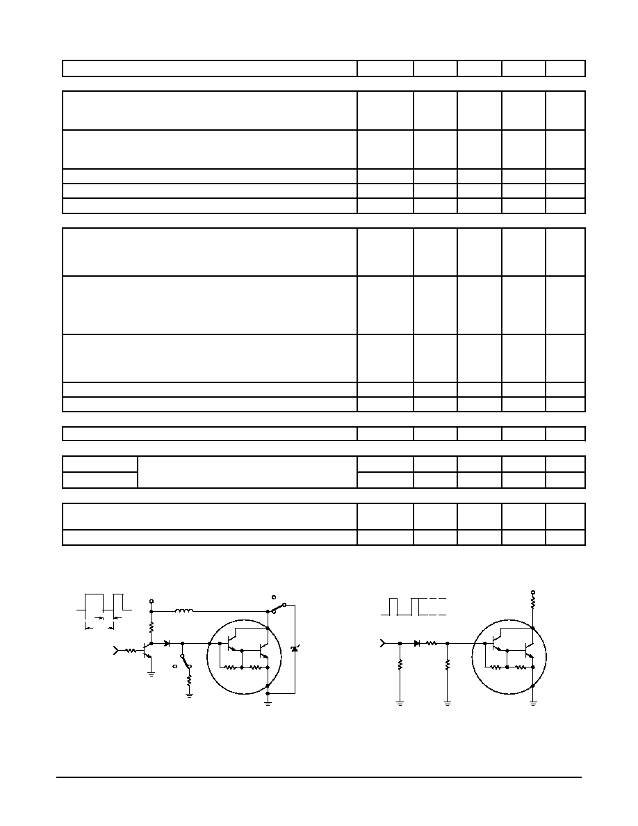
0 V
t1
20 ms
*
470
1K
30
L
47
1N4001
BC337
VCEO
VCER
100
B
TUT
C
*
E
Vclamp
UNCLAMPED
CLAMPED
* Adjust t1 such that
*
IC reaches Required
*
value.
VCC = 16 Vdc
ftest = 200 Hz
PULSE WIDTH = 1 ms
1K
30
B
TUT
C
E
40
51
100
IB = 0.3 Adc
VCC = 12 Vdc
2
/20 W
IC = 6 Adc
15 Vdc
0 Vdc
1N4001
Figure 1. Sustaining Voltage Test Circuit
Figure 2. Switching Times Test Circuit
BU323AP
3≠3
Motorola Bipolar Power Transistor Device Data
, COLLECT
OR CURRENT
(
A)
µ
I C
V
CE
, COLLECT
OR≠EMITTER VOL
T
AGE (VOL
TS)
2000
0.1
Figure 3. DC Current Gain
IC, COLLECTOR CURRENT (AMP)
20
0.2
0.3
0.5 0.7
1
5
7
10
500
200
100
70
Figure 4. Collector Saturation Region
3
0.002
IB, BASE CURRENT (AMP)
0.5
0.005 0.01
0.02
0.05
0.2
0.5
1
2
2.5
2
1.5
1
IC = 0.5 A
TJ = 25
∞
C
3
10 A
700
300
h
FE
, DC CURRENT
GAIN
TJ = 150
∞
C
25
∞
C
50
30
2
3
0.1
1.7
0.1
Figure 5. Collector≠Emitter Saturation Voltage
IC, COLLECTOR CURRENT (A)
0.2
0.5
1.0
2.0
10
1.6
1.4
1.3
0.5
IC/IB = 50
TJ = 25
∞
C
1.5
Figure 6. Base≠Emitter Voltage
1000
VCE = 3 Vdc
VCE = 6 Vdc
6
V
CE(sat)
, COLLECT
OR≠EMITTER SA
TURA
TION VOL
T
AGE (V)
1.2
1.1
0.9
0.8
1.0
0.7
0.6
5.0
2.2
0.1
IC, COLLECTOR CURRENT (A)
0.2
0.5
1.0
2.0
10
2.1
1.9
1.8
1.0
2.0
1.7
1.6
1.4
1.3
1.5
1.2
1.1
5.0
TJ = 25
∞
C
Figure 7. Turn≠Off Switching Time
10
0.2
IC, COLLECTOR CURRENT (AMP)
0.1
0.3
0.5 0.7
1
3
5
20
TJ = 25
∞
C
IC/IB = 20
VCE = 12 Vdc
t,
TIME (
s)
µ
2
7
5
3
2
1
ts
0.7
0.5
0.3
0.2
7
10
tf
Figure 8. Collector Cutoff Region
104
≠ 0.2
VBE, BASE≠EMITTER VOLTAGE (VOLTS)
10 ≠1
0
+ 0.2
103
102
101
100
+ 0.4
+ 0.6
+ 0.8
REVERSE
VCE = 250 Vdc
TJ = 150
∞
C
IC = ICES
75
∞
C
25
∞
C
TJ = ≠ 40
∞
C
TJ = ≠ 40
∞
C
V
CE(sat)
, COLLECT
OR≠EMITTER SA
TURA
TION VOL
T
AGE (V)
FORWARD

BU323AP
3≠4
Motorola Bipolar Power Transistor Device Data
Figure 9. Thermal Response
t, TIME (ms)
1
0.01
0.01
0.5
0.2
0.1
0.05
0.02
r(t)
,
TRANSIENT
THERMAL
RESIST
ANCE
0.05
1
2
5
10
20
50
100
200
2000
500
R
JC(t) = r(t) R
JC
R
JC =
∞
C/W MAX
D CURVES APPLY FOR POWER
PULSE TRAIN SHOWN
READ TIME AT t1
TJ(pk) ≠ TC = P(pk) R
JC(t)
P(pk)
t1
t2
DUTY CYCLE, D = t1/t2
D = 0.5
0.2
0.05
0.02
0.01
SINGLE PULSE
0.1
0.7
0.3
0.07
0.03
0.02
0.1
0.5
0.2
(NORMALIZED)
1000
50
5
Figure 10. Forward Bias Safe Operating Area
VCE, COLLECTOR≠EMITTER VOLTAGE (VOLTS)
20
10
5
1
0.005
30
70
BONDING WIRE LIMIT
THERMAL LIMIT (SINGLE PULSE)
SECOND BREAKDOWN LIMIT
I C
, COLLECT
OR CURRENT
(AMP)
dc
100
µ
s
0.2
0.01
10
20
5.0 ms
1.0 ms
100
200 300
500
2
0.1
50
TC = 25
∞
C
There are two limitations on the power handling ability of a
transistor average junction temperature and second break-
down. Safe operating area curves indicate IC ≠ VCE limits of
the transistor that must be observed for reliable operation,
i.e., the transistor must not be subjected to greater dissipa-
tion than the curves indicate.
The data of Figure 10 is based on TC = 25
_
C, TJ(pk) is
variable depending on power level. Second breakdown pulse
limits are valid for duty cycles to 10% but must be derated
when TC
25
_
C. Second breakdown limitations do not der-
ate the same as thermal limitations. Allowable current at the
voltages shown on Figure 10 may be found at any case tem-
perature by using the appropriate curve on Figure 11.
TJ(pk) may be calculated from the data in Figure 11. At high
case temperatures, thermal limitations will reduce the power
that can be handled to values less than the limitations im-
posed by second breakdown.
100
0
Figure 11. Power Derating
TC, CASE TEMPERATURE (
∞
C)
80
0
80
120
POWER DERA
TING F
ACT
OR (%)
40
20
40
160
200
60
THERMAL
DERATING
SECOND BREAKDOWN
DERATING
Figure 12. Ignition Test Circuit
0 Vdc
t1
50 ms
1K
30
B
470
VCC = 16 Vdc
1N4001
BC337
47
VZ
C
E
TUT
2.2
0.22
µ
F
100
1N4001
<1
11 mH
INDUCTIVE LOAD
t1 to be selected such that IC reaches 10 Adc before switch≠off.
NOTE: Figure 12 specifies energy handling capabilities in an automotive ignition circuit.
VZ = 350 V (BU323P)
VZ =
400 V (BU323AP)
at IZ = 20 mA