MOTOROLA
SEMICONDUCTOR
TECHNICAL DATA
Motorola TVS/Zener Device Data
7-139
225 mW SOT-23 Data Sheet
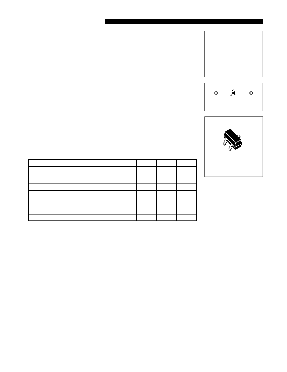
225 mW SOT-23
Zener Voltage Regulator Diodes
GENERAL DATA APPLICABLE TO ALL SERIES IN
THIS GROUP
Zener Voltage
Regulator Diodes
Manufacturing Locations:
WAFER FAB: Phoenix, Arizona
ASSEMBLY: Seremban, Malaysia
TEST: Seremban, Malaysia
MAXIMUM CASE TEMPERATURE FOR SOLDERING
PURPOSES: 260
∞
C for 10 seconds
THERMAL CHARACTERISTICS
Characteristic
Symbol
Max
Unit
Total Device Dissipation FR-5 Board,*
TA = 25
∞
C
Derate above 25
∞
C
PD
225
1.8
mW
mW/
∞
C
Thermal Resistance Junction to Ambient
R
JA
556
∞
C/W
Total Device Dissipation
Alumina Substrate,** TA = 25
∞
C
Derate above 25
∞
C
PD
300
2.4
mW
mW/
∞
C
Thermal Resistance Junction to Ambient
R
JA
417
∞
C/W
Junction and Storage Temeprature
TJ, Tstg
150
∞
C
*
*FR-5 = 1.0 x 0.75 x 0.62 in.
**Alumina = 0.4 x 0.3 x 0.024 in. 99.5% alumina.
GENERAL
DATA
CASE 318-07, STYLE 8
SOT-23 (TO-236AB)
PLASTIC
225 mW
SOT-23
1
2
3
3
Cathode
1
Anode
GENERAL DATA -- 225 mW SOT-23
Motorola TVS/Zener Device Data
7-140
225 mW SOT-23 Data Sheet
TYPICAL CHARACTERISTICS
VZ
, TEMPERA
TURE COEFFICIENT
(mV/
C)
∞
VZ, NOMINAL ZENER VOLTAGE (V)
≠ 3
≠ 2
≠1
0
1
2
3
4
5
6
7
8
12
11
10
9
8
7
6
5
4
3
2
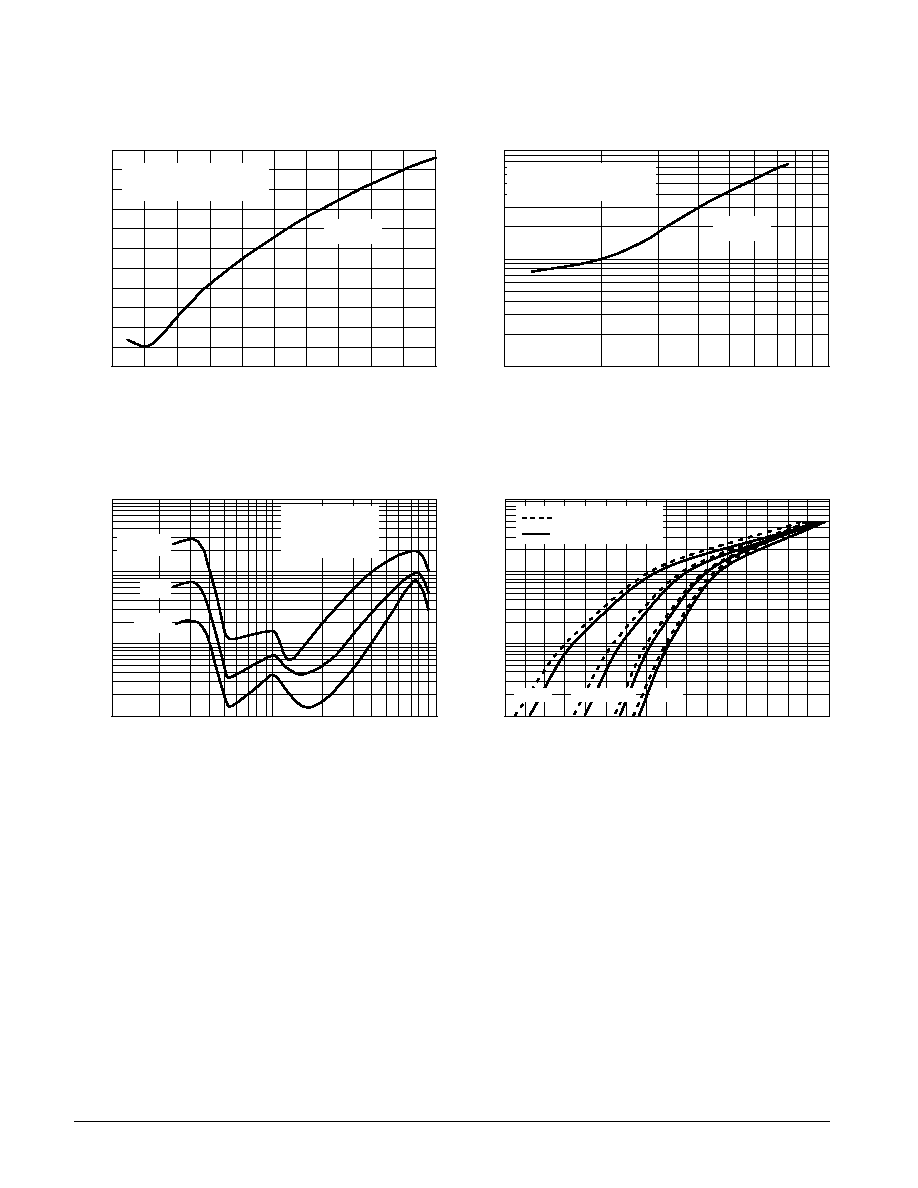
Figure 1. Temperature Coefficients
(Temperature Range ≠ 55
∞
C to +150
∞
C)
TYPICAL TC VALUES
FOR MMBZ5221BLT1 SERIES
VZ @ IZT
VZ
, TEMPERA
TURE COEFFICIENT
(mV/
C)
∞
100
10
1
10
100
VZ, NOMINAL ZENER VOLTAGE (V)
Figure 2. Temperature Coefficients
(Temperature Range ≠ 55
∞
C to +150
∞
C)
TYPICAL TC VALUES
FOR MMBZ5221BLT1 SERIES
VZ @ IZT
100
VZ, NOMINAL ZENER VOLTAGE
Figure 3. Effect of Zener Voltage on
Zener Impedance
10
1
Z
ZT
, DYNAMIC IMPEDANCE (
)
1000
100
10
1
TJ = 25
∞
C
IZ(AC) = 0.1 IZ(DC)
f = 1 kHz
IZ = 1 mA
5 mA
20 mA
VF, FORWARD VOLTAGE (V)
Figure 4. Typical Forward Voltage
1.2
1.1
1.0
0.9
0.8
0.7
0.6
0.5
0.4
I F
, FOR
W
ARD
CURRENT
(mA)
1000
100
10
1
75 V (MMBZ5267BLT1)
91 V (MMBZ5270BLT1)
150
∞
C
75
∞
C 25
∞
C
0
∞
C
GENERAL DATA -- 225 mW SOT-23
Motorola TVS/Zener Device Data
7-141
225 mW SOT-23 Data Sheet
TYPICAL CHARACTERISTICS
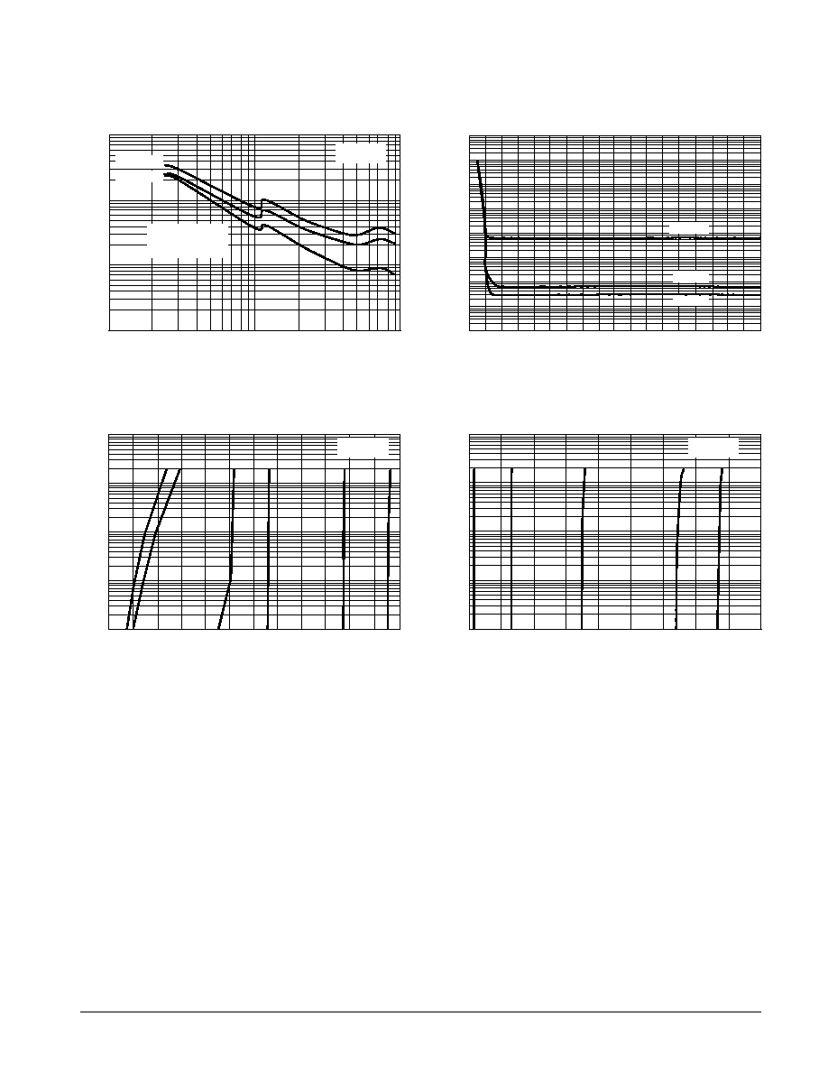
C, CAP
ACIT
ANCE
(pF)
100
VZ, NOMINAL ZENER VOLTAGE (V)
Figure 5. Typical Capacitance
1000
100
10
1
10
1
BIAS AT
50% OF VZ NOM
TA = 25
∞
C
0 V BIAS
1 V BIAS
12
VZ, ZENER VOLTAGE (V)
Figure 7. Zener Voltage versus Zener Current
(VZ Up to 12 V)
100
10
1
0.1
0.01
10
8
6
4
2
0
TA = 25
∞
C
I Z
, ZENER CURRENT
(mA)
VZ, ZENER VOLTAGE (V)
Figure 8. Zener Voltage versus Zener Current
(12 V to 91 V)
100
10
1
0.1
0.01
10
30
50
70
90
TA = 25
∞
C
I R
, LEAKAGE CURRENT
(
A
)
µ
90
VZ, NOMINAL ZENER VOLTAGE (V)
Figure 6. Typical Leakage Current
1000
100
10
1
0.1
0.01
0.001
0.0001
0.00001
80
70
60
50
40
30
20
10
0
+150
∞
C
+ 25
∞
C
≠ 55
∞
C
I Z
, ZENER CURRENT
(mA)

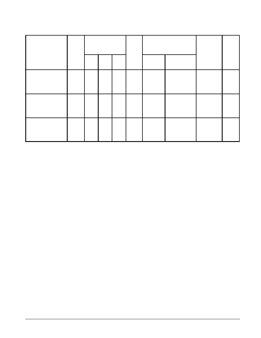
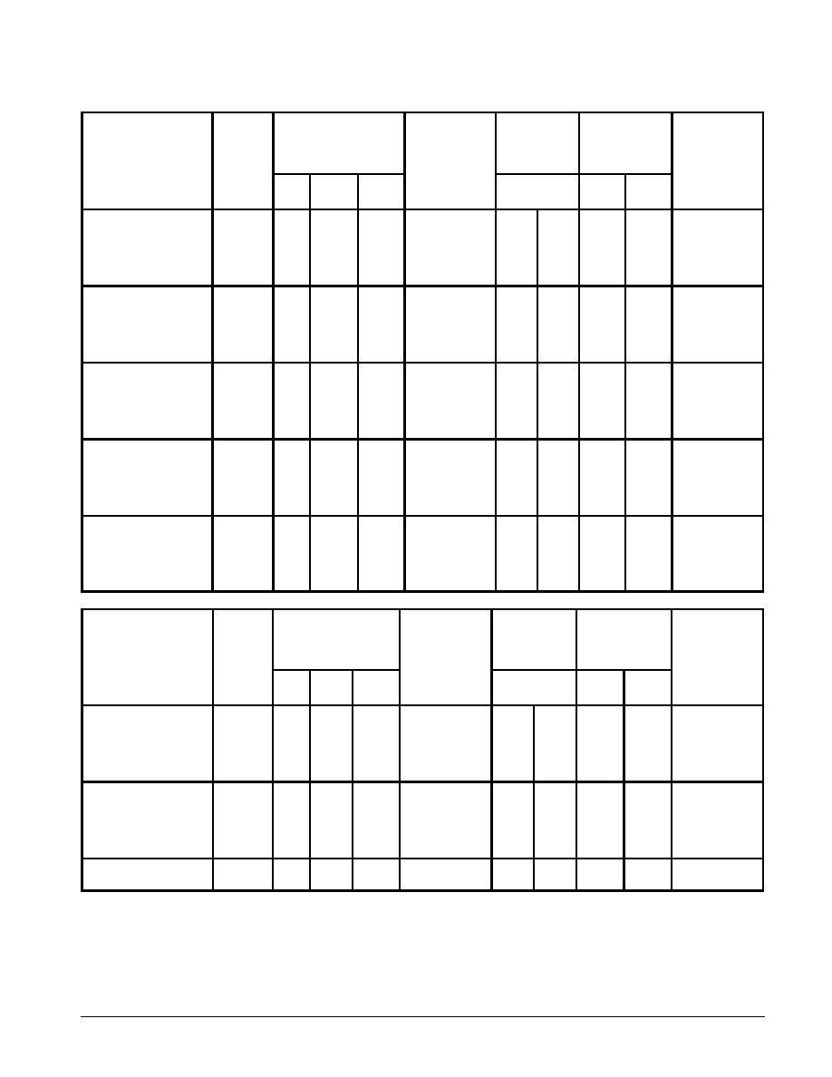
Type
Number
Max Zener
Impedance
ZZT1
(Ohms)
@ IZT1 =
5 mA
Max Zener
Impedance
ZZT2
(Ohms)
@ IZT2 =
1 mA
Max Zener
Impedance
ZZT3
(Ohms)
@ IZT3 =
20 mA
IR
µ
A
@
VR
Volts
C pF
Max
@ VR = 0
f = 1 MHz
GENERAL DATA -- 225 mW SOT-23
Motorola TVS/Zener Device Data
7-142
225 mW SOT-23 Data Sheet
ELECTRICAL CHARACTERISTICS (Pinout: 1-Anode, 2-NC, 3-Cathode)
(VF = 0.9 V Max @ IF = 10 mA for all types)
Zener Voltage
VZ1 (Volts)
@ IZT1 = 5 mA
(Note 1)
Max
Reverse
Leakage
Current
Zener Voltage
VZ2 (Volts)
@ IZT2 = 1 mA
(Note 1)
Zener Voltage
VZ3 (Volts)
@ IZT3 = 20 mA
(Note 1)
dVZ/dt
(mV/k)
@ IZT1 = 5 mA
Marking
Nom
Min
Max
Min
Max
Min
Max
Min
Max
BZX84C2V4LT1
Z11
2.4
2.2
2.6
100
50
1
1.7
2.1
600
2.6
3.2
50
≠3.5
0
450
BZX84C2V7LT1
Z12
2.7
2.5
2.9
100
20
1
1.9
2.4
600
3
3.6
50
≠3.5
0
450
BZX84C3V0LT1
Z13
3
2.8
3.2
95
10
1
2.1
2.7
600
3.3
3.9
50
≠3.5
0
450
BZX84C3V3LT1
Z14
3.3
3.1
3.5
95
5
1
2.3
2.9
600
3.6
4.2
40
≠3.5
0
450
BZX84C3V6LT1
Z15
3.6
3.4
3.8
90
5
1
2.7
3.3
600
3.9
4.5
40
≠3.5
0
450
BZX84C3V9LT1
Z16
3.9
3.7
4.1
90
3
1
2.9
3.5
600
4.1
4.7
30
≠3.5
≠2.5
450
BZX84C4V3LT1
W9
4.3
4
4.6
90
3
1
3.3
4
600
4.4
5.1
30
≠3.5
0
450
BZX84C4V7LT1
Z1
4.7
4.4
5
80
3
2
3.7
4.7
500
4.5
5.4
15
≠3.5
0.2
260
BZX84C5V1LT1
Z2
5.1
4.8
5.4
60
2
2
4.2
5.3
480
5
5.9
15
≠2.7
1.2
225
BZX84C5V6LT1
Z3
5.6
5.2
6
40
1
2
4.8
6
400
5.2
6.3
10
≠2.0
2.5
200
BZX84C6V2LT1
Z4
6.2
5.8
6.6
10
3
4
5.6
6.6
150
5.8
6.8
6
0.4
3.7
185
BZX84C6V8LT1
Z5
6.8
6.4
7.2
15
2
4
6.3
7.2
80
6.4
7.4
6
1.2
4.5
155
BZX84C7V5LT1
Z6
7.5
7
7.9
15
1
5
6.9
7.9
80
7
8
6
2.5
5.3
140
BZX84C8V2LT1
Z7
8.2
7.7
8.7
15
0.7
5
7.6
8.7
80
7.7
8.8
6
3.2
6.2
135
BZX84C9V1LT1
Z8
9.1
8.5
9.6
15
0.5
6
8.4
9.6
100
8.5
9.7
8
3.8
7.0
130
BZX84C10LT1
Z9
10
9.4
10.6
20
0.2
7
9.3
10.6
150
9.4
10.7
10
4.5
8.0
130
BZX84C11LT1
Y1
11
10.4
11.6
20
0.1
8
10.2
11.6
150
10.4
11.8
10
5.4
9.0
130
BZX84C12LT1
Y2
12
11.4
12.7
25
0.1
8
11.2
12.7
150
11.4
12.9
10
6.0
10.0
130
BZX84C13LT1
Y3
13
12.4
14.1
30
0.1
8
12.3
14
170
12.5
14.2
15
7.0
11.0
120
BZX84C15LT1
Y4
15
13.8
15.6
30
0.05
10.5
13.7
15.5
200
13.9
15.7
20
9.2
13.0
110
BZX84C16LT1
Y5
16
15.3
17.1
40
0.05
11.2
15.2
17
200
15.4
17.2
20
10.4
14.0
105
BZX84C18LT1
Y6
18
16.8
19.1
45
0.05
12.6
16.7
19
225
16.9
19.2
20
12.4
16.0
100
BZX84C20LT1
Y7
20
18.8
21.2
55
0.05
14
18.7
21.1
225
18.9
21.4
20
14.4
18.0
85
BZX84C22LT1
Y8
22
20.8
23.3
55
0.05
15.4
20.7
23.2
250
20.9
23.4
25
16.4
20.0
85
BZX84C24LT1
Y9
24
22.8
25.6
70
0.05
16.8
22.7
25.5
250
22.9
25.7
25
18.4
22.0
80
VZ1 Below
@ IZT1 = 2 mA
ZZT1
Below
@ IZT1 =
2 mA
VZ2 Below
@ IZT2 = 0.1 mA
ZZT2
Below
@ IZT4 =
0.5 mA
(Note 2)
VZ3 Below
@ IZT3 = 10 mA
ZZT3
Below
@ IZT3 =
10 mA
dVZ/dt
(mV/k) Below
@ IZT1 = 2 mA
BZX84C27LT1
Y10
27
25.1
28.9
80
0.05
18.9
25
28.9
300
25.2
29.3
45
21.4
25.3
70
BZX84C30LT1
Y11
30
28
32
80
0.05
21
27.8
32
300
28.1
32.4
50
24.4
29.4
70
BZX84C33LT1
Y12
33
31
35
80
0.05
23.1
30.8
35
325
31.1
35.4
55
27.4
33.4
70
BZX84C36LT1
Y13
36
34
38
90
0.05
25.2
33.8
38
350
34.1
38.4
60
30.4
37.4
70
BZX84C39LT1
Y14
39
37
41
130
0.05
27.3
36.7
41
350
37.1
41.5
70
33.4
41.2
45
BZX84C43LT1
Y15
43
40
46
150
0.05
30.1
39.7
46
375
40.1
46.5
80
37.6
46.6
40
BZX84C47LT1
Y16
47
44
50
170
0.05
32.9
43.7
50
375
44.1
50.5
90
42.0
51.8
40
BZX84C51LT1
Y17
51
48
54
180
0.05
35.7
47.6
54
400
48.1
54.6
100
46.6
57.2
40
BZX84C56LT1
Y18
56
52
60
200
0.05
39.2
51.5
60
425
52.1
60.8
110
52.2
63.8
40
BZX84C62LT1
Y19
62
58
66
215
0.05
43.4
57.4
66
450
58.2
67
120
58.8
71.6
35
BZX84C68LT1
Y20
68
64
72
240
0.05
47.6
63.4
72
475
64.2
73.2
130
65.6
79.8
35
BZX84C75LT1
Y21
75
70
79
255
0.05
52.5
69.4
79
500
70.3
80.2
140
73.4
88.6
35
NOTES: 1. Zener voltage is measured with a pulse test current (IZ) applied at an ambient temperature of 25
∞
C.
NOTES:
2. The zener impedance, ZZT2, for the 27 through 75 volt types is tested at 0.5 mA rather than the test current of 0.1 mA used for VZ2.

GENERAL DATA -- 225 mW SOT-23
Motorola TVS/Zener Device Data
7-143
225 mW SOT-23 Data Sheet
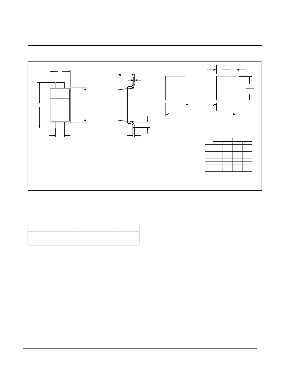
225 mW SOT-23
MULTIPLE PACKAGE QUANTITY (MPQ)
REQUIREMENTS
Zener Voltage Regulator Diodes -- Surface Mounted
CASE 318-07
PLASTIC
(Refer to Section 10 for Surface Mount, Thermal Data and Footprint Information.)
(Refer to Section 10 for more information on Packaging Specifications.)
Package Option
Tape and Reel
3K
Type No. Suffix
T1
MPQ (Units)
Tape and Ammo
T3
10K
MIN
MIN
MAX
MAX
INCHES
MILLIMETERS
DIM
A
B
C
D
G
H
J
K
L
S
V
2.80
1.20
0.89
0.37
1.78
0.013
0.085
0.45
0.89
2.10
0.45
3.04
1.40
1.11
0.50
2.04
0.100
0.177
0.60
1.02
2.50
0.60
0.1102
0.0472
0.0350
0.0150
0.0701
0.0005
0.0034
0.0180
0.0350
0.0830
0.0177
0.1197
0.0551
0.0440
0.0200
0.0807
0.0040
0.0070
0.0236
0.0401
0.0984
0.0236
NOTES:
1. DIMENSIONING AND TOLERANCING PER
ANSI Y14.5M, 1982.
2. CONTROLLING DIMENSION: INCH.
3. MAXIMUM LEAD THICKNESS INCLUDES
LEAD FINISH THICKNESS. MINIMUM LEAD
THICKNESS IS THE MINIMUM THICKNESS
OF BASE MATERIAL.
A
L
S
V
G
1
2
3
C
K
J
B
D
H
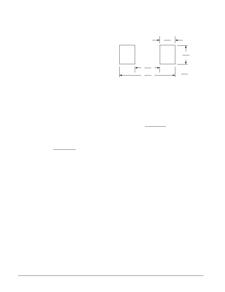
SOT-23 Footprint
mm
inches
0.037
0.95
0.037
0.95
0.079
2.0
0.035
0.9
0.031
0.8
STYLE 8:
PIN 1. ANODE
2. NO CONNECTION
3. CATHODE

GENERAL DATA -- 225 mW SOT-23
Motorola TVS/Zener Device Data
7-144
225 mW SOT-23 Data Sheet
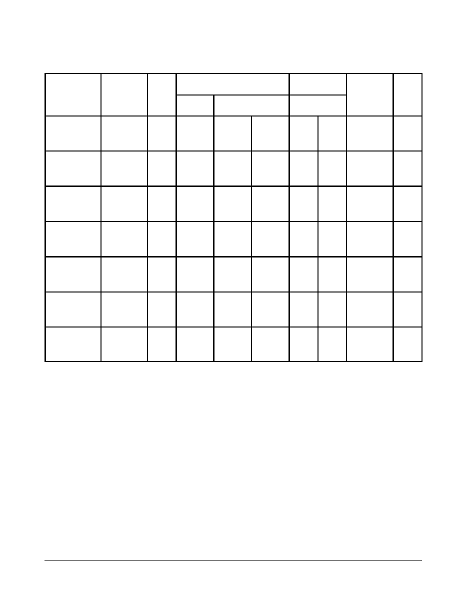
ELECTRICAL CHARACTERISTICS (Pinout: 1-Anode, 2-NC, 3-Cathode)
(VF = 0.9 V Max @ IF = 10 mA for all types.)
Device
Marking
Test
Current
IZT
mA
Zener
Voltage
VZ (
±
5%)
Nominal
(Note 1)
ZZK
IZ = 0.25 mA
Max
ZZT
IZ = IZT
@ 10% Mod
Max
Max
IR
µ
A
VR
V
@
MMBZ5221BLT1
18A
20
2.4
1200
30
100
1
MMBZ5222BLT1
18B
20
2.5
1250
30
100
1
MMBZ5223BLT1
18C
20
2.7
1300
30
75
1
MMBZ5224BLT1
18D
20
2.8
1400
30
75
1
MMBZ5225BLT1
18E
20
3
1600
29
50
1
MMBZ5226BLT1
8A
20
3.3
1600
28
25
1
MMBZ5227BLT1
8B
20
3.6
1700
24
15
1
MMBZ5228BLT1
8C
20
3.9
1900
23
10
1
MMBZ5229BLT1
8D
20
4.3
2000
22
5
1
MMBZ5230BLT1
8E
20
4.7
1900
19
5
2
MMBZ5231BLT1
8F
20
5.1
1600
17
5
2
MMBZ5232BLT1
8G
20
5.6
1600
11
5
3
MMBZ5233BLT1
8H
20
6
1600
7
5
3.5
MMBZ5234BLT1
8J
20
6.2
1000
7
5
4
MMBZ5235BLT1
8K
20
6.8
750
5
3
5
MMBZ5236BLT1
8L
20
7.5
500
6
3
6
MMBZ5237BLT1
8M
20
8.2
500
8
3
6.5
MMBZ5238BLT1
8N
20
8.7
600
8
3
6.5
MMBZ5239BLT1
8P
20
9.1
600
10
3
7
MMBZ5240BLT1
8Q
20
10
600
17
3
8
MMBZ5241BLT1
8R
20
11
600
22
2
8.4
MMBZ5242BLT1
8S
20
12
600
30
1
9.1
MMBZ5243BLT1
8T
9.5
13
600
13
0.5
9.9
MMBZ5244BLT1
8U
9
14
600
15
0.1
10
MMBZ5245BLT1
8V
8.5
15
600
16
0.1
11
MMBZ5246BLT1
8W
7.8
16
600
17
0.1
12
MMBZ5247BLT1
8X
7.4
17
600
19
0.1
13
MMBZ5248BLT1
8Y
7
18
600
21
0.1
14
MMBZ5249BLT1
8Z
6.6
19
600
23
0.1
14
MMBZ5250BLT1
81A
6.2
20
600
25
0.1
15
MMBZ5251BLT1
81B
5.6
22
600
29
0.1
17
MMBZ5252BLT1
81C
5.2
24
600
33
0.1
18
MMBZ5253BLT1
81D
5
25
600
35
0.1
19
MMBZ5254BLT1
81E
4.6
27
600
41
0.1
21
MMBZ5255BLT1
81F
4.5
28
600
44
0.1
21
MMBZ5256BLT1
81G
4.2
30
600
49
0.1
23
MMBZ5257BLT1
81H
3.8
33
700
58
0.1
25
MMBZ5258BLT1
81J
3.4
36
700
70
0.1
27
MMBZ5259BLT1
81K
3.2
39
800
80
0.1
30
MMBZ5260BLT1
18F
3
43
900
93
0.1
33
MMBZ5261BLT1
81M
2.7
47
1000
105
0.1
36
MMBZ5262BLT1
81N
2.5
51
1100
125
0.1
39
MMBZ5263BLT1
81P
2.2
56
1300
150
0.1
43
MMBZ5264BLT1
81Q
2.1
60
1400
170
0.1
46
MMBZ5265BLT1
81R
2
62
1400
185
0.1
47
MMBZ5266BLT1
81S
1.8
68
1600
230
0.1
52
MMBZ5267BLT1
81T
1.7
75
1700
270
0.1
56
MMBZ5268BLT1
81U
1.5
82
2000
330
0.1
62
MMBZ5269BLT1
81V
1.4
87
2200
370
0.1
68
MMBZ5270BLT1
81W
1.4
91
2300
400
0.1
69
NOTE 1. Zener voltage is measured with a pulse test current (IZT) applied at an ambient temperature of 25
∞
C.

MOTOROLA
SEMICONDUCTOR
TECHNICAL DATA
Motorola TVS/Zener Device Data
7-145
500 mW Leadless (SOD-123) Data Sheet
Designer's
TM
Data Sheet
Surface Mount Silicon Zener Diodes
Plastic SOD 123 Package
Three complete series of Zener Diodes are offered in the convenient, surface mount
plastic SOD-123 package. These devices provide a convenient alternative to the leadless
34 package style.
∑
500 mW Rating on FR-4 or FR-5 Board
∑
Package Designed for Optimal Automated Board Assembly
∑
Corrosion Resistant Finish, Easily Solderable
∑
ESD Rating of Class 3 (exceeding 16 kV) per the Human Body Model
∑
Small Package Size for High Density Applications
∑
Available in 8 mm Tape and Reel
Add "T1" to the device number to order the 7 inch / 3000 unit reel.
Add "T3" to the device number to order the 13 inch / 10,000 unit reel.
∑
Wafer Fab Location: Phoenix, Arizona
Assembly/Test Location: Seremban, Malaysia
MMSZ5221BT1 thru MMSZ5270BT1
∑
General Purpose, Medium Current
∑
Wide Voltage Range -- 2.4 to 91 Volts
MMSZ4678T1 thru MMSZ4717T1
∑
Low Operating Currents, Low Leakage, Sharp Breakdown Characteristics
∑
Wide Voltage Range -- 1.8 to 43 Volts
MMSZ2V4T1 thru MMSZ75T1
∑
Specified Similar to European BZV55C Series
∑
Wide Voltage Range -- 2.4 to 75 Volts
DEVICE RATING
(TA = 25
∞
C unless otherwise noted)
Rating
Symbol
Value
Unit
Power Dissipation on FR-4 or FR-5 Board [1]
Derate above TL = 75
∞
C
PD
--
500
6.7
mW
mW/
∞
C
Thermal Resistance Junction to Lead [2]
Thermal Resistance Junction to Ambient [2]
R
JL
R
JA
150
340
∞
C/W
Junction Temperature Range
TJ
≠55 to +150
∞
C
Storage Temperature Range
Tstg
≠55 to +150
∞
C
Lead Solder Temperature ≠ Maximum (10 sec. duration)
--
260
∞
C
[1] FR-4 or FR-5 = 3.5 x 1.5 inches, using the Motorola minimum recommended footprint as shown in Figure 11.
[2] Thermal Resistance measurement obtained via Infrared Scan Method
Designer's Data for "Worst Case'' Conditions -- The Designer's Data Sheet permits the design of most circuits entirely from the information presented. Limit curves -- representing
boundaries on device characteristics -- are given to facilitate "worst case'' design.
Designer's is a trademark of Motorola, Inc.
Thermal Clad is a trademark of the Bergquist Company.
Preferred devices are Motorola recommended choices for future use and best overall value.
MMSZ5221BT1-
MMSZ5270BT1*
MMSZ4678T1-
MMSZ4717T1
MMSZ2V4T1-
MMSZ75T1
PLASTIC SURFACE
MOUNT
ZENER DIODES
500 MILLIWATTS
1.8 ≠ 91 VOLTS
CASE 425, STYLE 1
PLASTIC
*Motorola Preferred Device Series
1: CATHODE
2: ANODE
1
2

MMSZ5221BT1, MMSZ4678T1, MMSZ2V4T1 Series
Motorola TVS/Zener Device Data
7-146
500 mW Leadless (SOD-123) Data Sheet
TYPICAL CHARACTERISTICS
VZ
, TEMPERA
TURE COEFFICIENT
(mV/
C)
∞
VZ, NOMINAL ZENER VOLTAGE (V)
≠ 3
≠ 2
≠1
0
1
2
3
4
5
6
7
8
12
11
10
9
8
7
6
5
4
3
2
Figure 1. Temperature Coefficients
(Temperature Range ≠ 55
∞
C to +150
∞
C)
TYPICAL TC VALUES
FOR MMSZ5221BT1 SERIES
VZ @ IZT
VZ
, TEMPERA
TURE COEFFICIENT
(mV/
C)
∞
100
10
1
10
100
VZ, NOMINAL ZENER VOLTAGE (V)
Figure 2. Temperature Coefficients
(Temperature Range ≠ 55
∞
C to +150
∞
C)
VZ @ IZT
P
D
, POWER DISSIP
A
TION (W
A
TTS)
1.2
1.0
0.8
0.6
0.4
0.2
0
150
125
100
75
50
25
0
T, TEMPERATURE (
∞
C)
Figure 3. Steady State Power Derating
PD versus TA
PD versus TL
P
pk
, PEAK SURGE POWER (W
A
TTS)
0.1
PW, PULSE WIDTH (ms)
Figure 4. Maximum Nonrepetitive Surge Power
1
10
100
1000
1000
100
10
1
RECTANGULAR
WAVEFORM, TA = 25
∞
C
100
VZ, NOMINAL ZENER VOLTAGE
Figure 5. Effect of Zener Voltage on
Zener Impedance
10
1
Z
ZT
, DYNAMIC IMPEDANCE (
)
1000
100
10
1
TJ = 25
∞
C
IZ(AC) = 0.1 IZ(DC)
f = 1 kHz
IZ = 1 mA
5 mA
20 mA
VF, FORWARD VOLTAGE (V)
Figure 6. Typical Forward Voltage
1.2
1.1
1.0
0.9
0.8
0.7
0.6
0.5
0.4
I F
, FOR
W
ARD
CURRENT
(mA)
1000
100
10
1
75 V (MMSZ5267BT1)
91 V (MMSZ5270BT1)
150
∞
C
75
∞
C 25
∞
C
0
∞
C
TYPICAL TC VALUES
FOR MMSZ5221BT1 SERIES

MMSZ5221BT1, MMSZ4678T1, MMSZ2V4T1 Series
Motorola TVS/Zener Device Data
7-147
500 mW Leadless (SOD-123) Data Sheet
TYPICAL CHARACTERISTICS
C, CAP
ACIT
ANCE
(pF)
100
VZ, NOMINAL ZENER VOLTAGE (V)
Figure 7. Typical Capacitance
1000
100
10
1
10
1
BIAS AT
50% OF VZ NOM
TA = 25
∞
C
0 V BIAS
1 V BIAS
12
VZ, ZENER VOLTAGE (V)
Figure 9. Zener Voltage versus Zener Current
(VZ Up to 12 V)
100
10
1
0.1
0.01
10
8
6
4
2
0
TA = 25
∞
C
I Z
, ZENER CURRENT
(mA)
VZ, ZENER VOLTAGE (V)
Figure 10. Zener Voltage versus Zener Current
(12 V to 91 V)
100
10
1
0.1
0.01
10
30
50
70
90
TA = 25
∞
C
I R
, LEAKAGE CURRENT
(
A
)
µ
90
VZ, NOMINAL ZENER VOLTAGE (V)
Figure 8. Typical Leakage Current
1000
100
10
1
0.1
0.01
0.001
0.0001
0.00001
80
70
60
50
40
30
20
10
0
+150
∞
C
+ 25
∞
C
≠ 55
∞
C
I Z
, ZENER CURRENT
(mA)

MMSZ5221BT1, MMSZ4678T1, MMSZ2V4T1 Series
Motorola TVS/Zener Device Data
7-148
500 mW Leadless (SOD-123) Data Sheet
ELECTRICAL CHARACTERISTICS
(TA = 25
∞
C unless otherwise noted [1]), (VF = 0.9 V Max. @ IF = 10 mA for all types)
T
M
ki
Zener Voltage
VZ @ IZT
Volts
[1] [2]
Test
Current
IZT
Max Zener
Impedance [3]
Max Reverse
Leakage
Current
IR @ VR
Test
Voltage
Type
Number
Marking
Nom
Min
Max
IZT
mA
ZZT
@ IZ = IZT
ZZK
@ IZK = 0.25 mA
IR @ VR
µ
A
Voltage
VR
Volts
MMSZ5221BT1
C1
2.4
2.28
2.52
20
30
1200
100
1
MMSZ5222BT1
C2
2.5
2.38
2.63
20
30
1250
100
1
MMSZ5223BT1
C3
2.7
2.57
2.84
20
30
1300
75
1
MMSZ5224BT1
C4
2.8
2.66
2.94
20
30
1400
75
1
MMSZ5225BT1
C5
3.0
2.85
3.15
20
30
1600
50
1
MMSZ5226BT1
D1
3.3
3.14
3.47
20
28
1600
25
1
MMSZ5227BT1
D2
3.6
3.42
3.78
20
24
1700
15
1
MMSZ5228BT1
D3
3.9
3.71
4.10
20
23
1900
10
1
MMSZ5229BT1
D4
4.3
4.09
4.52
20
22
2000
5
1
MMSZ5230BT1
D5
4.7
4.47
4.94
20
19
1900
5
2
MMSZ5231BT1
E1
5.1
4.85
5.36
20
17
1600
5
2
MMSZ5232BT1
E2
5.6
5.32
5.88
20
11
1600
5
3
MMSZ5233BT1
E3
6.0
5.70
6.30
20
7
1600
5
3.5
MMSZ5234BT1
E4
6.2
5.89
6.51
20
7
1000
5
4
MMSZ5235BT1
E5
6.8
6.46
7.14
20
5
750
3
5
MMSZ5236BT1
F1
7.5
7.13
7.88
20
6
500
3
6
MMSZ5237BT1
F2
8.2
7.79
8.61
20
8
500
3
6.5
MMSZ5238BT1
F3
8.7
8.27
9.14
20
8
600
3
6.5
MMSZ5239BT1
F4
9.1
8.65
9.56
20
10
600
3
7
MMSZ5240BT1
F5
10
9.50
10.50
20
17
600
3
8
MMSZ5241BT1
H1
11
10.45
11.55
20
22
600
2
8.4
MMSZ5242BT1
H2
12
11.40
12.60
20
30
600
1
9.1
MMSZ5243BT1
H3
13
12.35
13.65
9.5
13
600
0.5
9.9
MMSZ5244BT1
H4
14
13.30
14.70
9.0
15
600
0.1
10
MMSZ5245BT1
H5
15
14.25
15.75
8.5
16
600
0.1
11
MMSZ5246BT1
J1
16
15.20
16.80
7.8
17
600
0.1
12
MMSZ5247BT1
J2
17
16.15
17.85
7.4
19
600
0.1
13
MMSZ5248BT1
J3
18
17.10
18.90
7.0
21
600
0.1
14
MMSZ5249BT1
J4
19
18.05
19.95
6.6
23
600
0.1
14
MMSZ5250BT1
J5
20
19.00
21.00
6.2
25
600
0.1
15
MMSZ5251BT1
K1
22
20.90
23.10
5.6
29
600
0.1
17
MMSZ5252BT1
K2
24
22.80
25.20
5.2
33
600
0.1
18
MMSZ5253BT1
K3
25
23.75
26.25
5.0
35
600
0.1
19
MMSZ5254BT1
K4
27
25.65
28.35
4.6
41
600
0.1
21
MMSZ5255BT1
K5
28
26.60
29.40
4.5
44
600
0.1
21
[1] Nominal zener voltage is measured with the device junction in thermal equilibrium at T
L = 30
∞
C
±
1
∞
C.
[2] All part numbers shown indicate a V
Z tolerance of
±
5%.
[3] Z
ZT and ZZK are measured by dividing the AC voltage drop across the device by the AC current applied. The specified limits are for IZ(AC) = 0.1 IZ(DC), with the AC frequency = 1 kHz.
MMSZ5221BT1, MMSZ4678T1, MMSZ2V4T1 Series
Motorola TVS/Zener Device Data
7-149
500 mW Leadless (SOD-123) Data Sheet
ELECTRICAL CHARACTERISTICS
(TA = 25
∞
C unless otherwise noted [1]), (VF = 0.9 V Max. @ IF = 10 mA for all types)
T
M
ki
Zener Voltage
VZ @ IZT
Volts
[1] [2]
Test
Current
IZT
Max Zener
Impedance [3]
Max Reverse
Leakage
Current
IR @ VR
Test
Voltage
Type
Number
Marking
Nom
Min
Max
IZT
mA
ZZT
@ IZ = IZT
ZZK
@ IZK = 0.25 mA
IR @ VR
µ
A
Voltage
VR
Volts
MMSZ5256BT1
M1
30
28.50
31.50
4.2
49
600
0.1
23
MMSZ5257BT1
M2
33
31.35
34.65
3.8
58
700
0.1
25
MMSZ5258BT1
M3
36
34.20
37.80
3.4
70
700
0.1
27
MMSZ5259BT1
M4
39
37.05
40.95
3.2
80
800
0.1
30
MMSZ5260BT1
M5
43
40.85
45.15
3.0
93
900
0.1
33
MMSZ5261BT1
N1
47
44.65
49.35
2.7
105
1000
0.1
36
MMSZ5262BT1
N2
51
48.45
53.55
2.5
125
1100
0.1
39
MMSZ5263BT1
N3
56
53.20
58.80
2.2
150
1300
0.1
43
MMSZ5264BT1
N4
60
57.00
63.00
2.1
170
1400
0.1
46
MMSZ5265BT1
N5
62
58.90
65.10
2.0
185
1400
0.1
47
MMSZ5266BT1
P1
68
64.60
71.40
1.8
230
1600
0.1
52
MMSZ5267BT1
P2
75
71.25
78.75
1.7
270
1700
0.1
56
MMSZ5268BT1
P3
82
77.90
86.10
1.5
330
2000
0.1
62
MMSZ5269BT1
P4
87
82.65
91.35
1.4
370
2200
0.1
68
MMSZ5270BT1
P5
91
86.45
95.55
1.4
400
2300
0.1
69
[1] Nominal zener voltage is measured with the device junction in thermal equilibrium at T
L = 30
∞
C
±
1
∞
C.
[2] All part numbers shown indicate a V
Z tolerance of
±
5%.
[3] Z
ZT and ZZK are measured by dividing the AC voltage drop across the device by the AC current applied. The specified limits are for IZ(AC) = 0.1 IZ(DC), with the AC frequency = 1 kHz.

MMSZ5221BT1, MMSZ4678T1, MMSZ2V4T1 Series
Motorola TVS/Zener Device Data
7-150
500 mW Leadless (SOD-123) Data Sheet
ELECTRICAL CHARACTERISTICS
(TA = 25
∞
C unless otherwise noted [1], (VF = 0.9 V Max. @ IF = 10 mA for all types)
Type
M
ki
Zener Voltage
VZ @ IZT = 50
µ
A
Volts
[1] [2]
Max Reverse
Leakage
Current
IR @ VR
Test
Voltage
VR
Type
Number
Marking
Nom
Min
Max
IR @ VR
µ
A
Volts
MMSZ4678T1
CC
1.8
1.71
1.89
7.5
1
MMSZ4679T1
CD
2.0
1.90
2.10
5
1
MMSZ4680T1
CE
2.2
2.09
2.31
4
1
MMSZ4681T1
CF
2.4
2.28
2.52
2
1
MMSZ4682T1
CH
2.7
2.57
2.84
1
1
MMSZ4683T1
CJ
3.0
2.85
3.15
0.8
1
MMSZ4684T1
CK
3.3
3.14
3.47
7.5
1.5
MMSZ4685T1
CM
3.6
3.42
3.78
7.5
2
MMSZ4686T1
CN
3.9
3.71
4.10
5
2
MMSZ4687T1
CP
4.3
4.09
4.52
4
2
MMSZ4688T1
CT
4.7
4.47
4.94
10
3
MMSZ4689T1
CU
5.1
4.85
5.36
10
3
MMSZ4690T1
CV
5.6
5.32
5.88
10
4
MMSZ4691T1
CA
6.2
5.89
6.51
10
5
MMSZ4692T1
CX
6.8
6.46
7.14
10
5.1
MMSZ4693T1
CY
7.5
7.13
7.88
10
5.7
MMSZ4694T1
CZ
8.2
7.79
8.61
1
6.2
MMSZ4695T1
DC
8.7
8.27
9.14
1
6.6
MMSZ4696T1
DD
9.1
8.65
9.56
1
6.9
MMSZ4697T1
DE
10
9.50
10.50
1
7.6
MMSZ4698T1
DF
11
10.45
11.55
0.05
8.4
MMSZ4699T1
DH
12
11.40
12.60
0.05
9.1
MMSZ4700T1
DJ
13
12.35
13.65
0.05
9.8
MMSZ4701T1
DK
14
13.30
14.70
0.05
10.6
MMSZ4702T1
DM
15
14.25
15.75
0.05
11.4
MMSZ4703T1
DN
16
15.20
16.80
0.05
12.1
MMSZ4704T1
DP
17
16.15
17.85
0.05
12.9
MMSZ4705T1
DT
18
17.10
18.90
0.05
13.6
MMSZ4706T1
DU
19
18.05
19.95
0.05
14.4
MMSZ4707T1
DV
20
19.00
21.00
0.01
15.2
MMSZ4708T1
DA
22
20.90
23.10
0.01
16.7
MMSZ4709T1
DZ
24
22.80
25.20
0.01
18.2
MMSZ4710T1
DY
25
23.75
26.25
0.01
19.00
MMSZ4711T1
EA
27
25.65
28.35
0.01
20.4
MMSZ4712T1
EC
28
26.60
29.40
0.01
21.2
MMSZ4713T1
ED
30
28.50
31.50
0.01
22.8
MMSZ4714T1
EE
33
31.35
34.65
0.01
25.0
MMSZ4715T1
EF
36
34.20
37.80
0.01
27.3
MMSZ4716T1
EH
39
37.05
40.95
0.01
29.6
MMSZ4717T1
EJ
43
40.85
45.15
0.01
32.6
[1] Nominal zener voltage is measured with the device junction in thermal equilibrium at T
L = 30
∞
C
±
1
∞
C.
[2] All part numbers shown indicate a V
Z tolerance of
±
5%
MMSZ5221BT1, MMSZ4678T1, MMSZ2V4T1 Series
Motorola TVS/Zener Device Data
7-151
500 mW Leadless (SOD-123) Data Sheet
ELECTRICAL CHARACTERISTICS
(TA = 25
∞
C unless otherwise noted), (VF = 0.9 V Max. @ IF = 10 mA for all types)
T
M
ki
Zener Voltage
VZ1 (Volts)
@ IZT1 = 5 mA
[1][2]
Max Zener
Impedance
ZZT1
@ IZT1 = 5 mA
Max
Reverse
Leakage
Current
Zener Voltage
VZ2 (Volts)
@ IZT2 = 1 mA
[1]
Max Zener
Impedance
ZZT2
@ IZT1 = 1 mA
Type
Number
Marking
Nom
Min
Max
@ IZT1 = 5 mA
[3]
IR @ VR
µ
A Volts
Min
Max
@ IZT1 = 1 mA
[3]
MMSZ2V4T1
T1
2.4
2.28
2.52
100
50
1
1.7
2.1
600
MMSZ2V7T1
T2
2.7
2.57
2.84
100
20
1
1.9
2.4
600
MMSZ3V0T1
T3
3.0
2.85
3.15
95
10
1
2.1
2.7
600
MMSZ3V3T1
T4
3.3
3.14
3.47
95
5
1
2.3
2.9
600
MMSZ3V6T1
T5
3.6
3.42
3.78
90
5
1
2.7
3.3
600
MMSZ3V9T1
U1
3.9
3.71
4.10
90
3
1
2.9
3.5
600
MMSZ4V3T1
U2
4.3
4.09
4.52
90
3
1
3.3
4.0
600
MMSZ4V7T1
U3
4.7
4.47
4.94
80
3
2
3.7
4.7
500
MMSZ5V1T1
U4
5.1
4.85
5.36
60
2
2
4.2
5.3
480
MMSZ5V6T1
U5
5.6
5.32
5.88
40
1
2
4.8
6.0
400
MMSZ6V2T1
V1
6.2
5.89
6.51
10
3
4
5.6
6.6
150
MMSZ6V8T1
V2
6.8
6.46
7.14
15
2
4
6.3
7.2
80
MMSZ7V5T1
V3
7.5
7.13
7.88
15
1
5
6.9
7.9
80
MMSZ8V2T1
V4
8.2
7.79
8.61
15
0.7
5
7.6
8.7
80
MMSZ9V1T1
V5
9.1
8.65
9.56
15
0.5
6
8.4
9.6
100
MMSZ10T1
A1
10
9.50
10.50
20
0.2
7
9.3
10.6
150
MMSZ11T1
A2
11
10.45
11.55
20
0.1
8
10.2
11.6
150
MMSZ12T1
A3
12
11.40
12.60
25
0.1
8
11.2
12.7
150
MMSZ13T1
A4
13
12.35
13.65
30
0.1
8
12.3
14.0
170
MMSZ15T1
A5
15
14.25
15.75
30
0.05
10.5
13.7
15.5
200
MMSZ16T1
X1
16
15.20
16.80
40
0.05
11.2
15.2
17.0
200
MMSZ18T1
X2
18
17.10
18.90
45
0.05
12.6
16.7
19.0
225
MMSZ20T1
X3
20
19.00
21.00
55
0.05
14
18.7
21.1
225
MMSZ22T1
X4
22
20.80
23.10
55
0.05
15.4
20.7
23.2
250
MMSZ24T1
X5
24
22.80
25.20
70
0.05
16.8
22.7
25.5
250
T
M
ki
Zener Voltage
VZ1 (Volts)
@ IZT1 = 2 mA
[1][2]
Max Zener
Impedance
ZZT1
@ IZT1 = 2 mA
Max
Reverse
Leakage
Current
Zener Voltage
VZ2 (Volts)
@ IZT2 = 0.1 mA
[1]
Max Zener
Impedance
ZZT2
@ IZT1 = 0.5 mA
Type
Number
Marking
Nom
Min
Max
@ IZT1 = 2 mA
[3]
IR @ VR
µ
A Volts
Min
Max
@ IZT1 = 0.5 mA
[3][4]
MMSZ27T1
Y1
27
25.65
28.35
80
0.05
18.9
25
28.9
300
MMSZ30T1
Y2
30
28.50
31.50
80
0.05
21
27.8
32
300
MMSZ33T1
Y3
33
31.35
34.65
80
0.05
23.1
30.8
35
325
MMSZ36T1
Y4
36
34.20
37.80
90
0.05
25.2
33.8
38
350
MMSZ39T1
Y5
39
37.05
40.95
130
0.05
27.3
36.7
41
350
MMSZ43T1
Z1
43
40.85
45.15
150
0.05
30.1
39.7
46
375
MMSZ47T1
Z2
47
44.65
49.35
170
0.05
32.9
43.7
50
375
MMSZ51T1
Z3
51
48.45
53.55
180
0.05
35.7
47.6
54
400
MMSZ56T1
Z4
56
53.20
58.80
200
0.05
39.2
51.5
60
425
MMSZ62T1
Z5
62
58.90
65.10
215
0.05
43.4
57.4
66
450
MMSZ68T1
Z6
68
64.60
71.40
240
0.05
47.6
63.4
72
475
MMSZ75T1
Z7
75
71.25
78.75
255
0.05
52.5
69.4
79
500
[1] Zener voltage is measured with the zener current applied for PW = 1.0 ms.
[2] All part numbers shown indicate a V
Z tolerance of
±
5%.
[3] Z
ZT1 and ZZT2 are measured by dividing the AC voltage drop across the device by the AC current applied. The specified limits are for IZ(AC) = 0.1 IZ(DC),
[3]
with the AC frequency = 1 kHz.
[4] The zener impedance, Z
ZT2, for the 27 through 75 volt types is tested at 0.5 mA rather than the test current of 0.1 mA used for VZ2.
MMSZ5221BT1, MMSZ4678T1, MMSZ2V4T1 Series
Motorola TVS/Zener Device Data
7-152
500 mW Leadless (SOD-123) Data Sheet
INFORMATION FOR USING THE SOD-123 SURFACE MOUNT PACKAGE
MINIMUM RECOMMENDED FOOTPRINTS FOR
SURFACE MOUNT APPLICATIONS
Surface mount board layout is a critical portion of the total
design. The footprint for the semiconductor packages must be
the correct size to ensure proper solder connection interface
between the board and the package.
The minimum recommended footprint for the SOD-123 is
shown at the right.
The SOD-123 package can be used on existing surface
mount boards which have been designed for the leadless 34
package style. The footprint compatibility makes conversion
from leadless 34 to SOD-123 straightforward.
…………
…………
…………
…………
…………
mm
inches
0.91
0.036
1.22
0.048
2.36
0.093
4.19
0.165
Figure 11. Minimum Recommended Footprint
SOD-123 POWER DISSIPATION
The power dissipation of the SOD-123 is a function of the
pad size. This can vary from the minimum pad size for
soldering to a pad size given for maximum power dissipation.
Power dissipation for a surface mount device is determined by
TJ(max), the maximum rated junction temperature of the die,
R
JA, the thermal resistance from the device junction to
ambient; and the operating temperature, TA. Using the values
provided on the data sheet for the SOD-123 package, PD can
be calculated as follows:
PD =
TJ(max) ≠ TA
R
JA
The values for the equation are found in the maximum
ratings table on the data sheet. Substituting these values into
the equation for an ambient temperature TA of 25
∞
C, one can
calculate the power dissipation of the device which in this case
is 0.37 watts.
PD =
150
∞
C ≠ 25
∞
C
340
∞
C/W
= 0.37 watts
The 340
∞
C/W for the SOD-123 package assumes using
recommended footprint shown on FR-4 glass epoxy printed
circuit board. Another alternative is to use a ceramic substrate
or an aluminum core board such as Thermal Clad
TM
. By using
an aluminum core board material such as Thermal Clad, the
power dissipation can be doubled using the same footprint.
GENERAL SOLDERING PRECAUTIONS
The melting temperature of solder is higher than the rated
temperature of the device. When the entire device is heated
to a high temperature, failure to complete soldering within a
short time could result in device failure. Therefore, the
following items should always be observed in order to
minimize the thermal stress to which the devices are
subjected.
∑
Always preheat the device.
∑
The delta temperature between the preheat and soldering
should be 100
∞
C or less.*
∑
When preheating and soldering, the temperature of the
leads and the case must not exceed the maximum
temperature ratings as shown on the data sheet. When
using infrared heating with the reflow soldering method,
the difference shall be a maximum of 10
∞
C.
∑
The soldering temperature and time shall not exceed
260
∞
C for more than 10 seconds.
∑
When shifting from preheating to soldering, the maximum
temperature gradient shall be 5
∞
C or less.
∑
After soldering has been completed, the device should be
allowed to cool naturally for at least three minutes.
Gradual cooling should be used as the use of forced
cooling will increase the temperature gradient and result
in latent failure due to mechanical stress.
∑
Mechanical stress or shock should not be applied during
cooling
* Soldering a device without preheating can cause excessive
thermal shock and stress which can result in damage to the
device.
Motorola TVS/Zener Device Data
7-153
500 mW Leadless (SOD-123) Data Sheet
500 mW SOD-123
MULTIPLE PACKAGE QUANTITY (MPQ)
REQUIREMENTS
Zener Voltage Regulator Diodes -- Surface Mounted
CASE 425
PLASTIC
(Refer to Section 10 for Surface Mount, Thermal Data and Footprint Information.)
(Refer to Section 10 for more information on Packaging Specifications.)
Package Option
Tape and Reel
3K
Type No. Suffix
T1(1)
MPQ (Units)
Tape and Reel
T3(2)
10K
NOTE: 1. The numbers on the suffixes indicate the following:
NOTE: 1.
1. 7
Reel. Cathode lead toward sprocket hole.
NOTE: 1.
2. 13
Reel. Cathode lead toward sprocket hole.
SOD-123 Footprint
………
………
………
………
………
…………
…………
…………
…………
…………
mm
inches
0.91
0.036
1.22
0.048
2.36
0.093
4.19
0.165
D
A
B
K
1
2
J
H
STYLE 1:
PIN 1. CATHODE
2. ANODE
E
¬¬¬
¬¬¬
C
0.055
0.100
0.037
0.020
0.010
0.000
--
0.140
0.071
0.112
0.053
0.028
--
0.004
0.006
0.152
1.80
2.85
1.35
0.70
--
0.10
0.15
3.85
1.40
2.55
0.95
0.50
0.25
0.00
--
3.55
MIN
MIN
MAX
MAX
MILLIMETERS
INCHES
DIM
A
B
C
D
E
H
J
K
NOTES:
1. DIMENSIONING AND TOLERANCING PER ANSI
Y14.5M, 1982.
2. CONTROLLING DIMENSION: INCH.
3. 425-01 THRU -03 OBSOLETE, NEW STANDARD
425-04.

MOTOROLA
SEMICONDUCTOR
TECHNICAL DATA
Motorola TVS/Zener Device Data
7-154
3 Watt DC Power Data Sheet
Devices listed in bold, italic are Motorola preferred devices.
3 Watt Plastic Surface Mount
Silicon Zener Diodes
This complete new line of 3 Watt Zener Diodes offers the following advantages.
Specification Features:
∑
A Complete Voltage Range -- 3.3 to 200 Volts
∑
Flat Handling Surface for Accurate Placement
∑
Package Design for Top Side or Bottom Circuit Board Mounting
∑
Available in Tape and Reel
Mechanical Characteristics:
CASE: Void-free, transfer-molded plastic
MAXIMUM CASE TEMPERATURE FOR SOLDERING PURPOSES: 260
∞
C for 10 seconds
FINISH: All external surfaces are corrosion resistant with readily solderable leads
POLARITY: Cathode indicated by molded polarity notch. When operated in zener mode,
cathode will be positive with respect to anode.
MOUNTING POSITION: Any
WEIGHT: Modified L-Bend providing more contact area to bond pad
WAFER FAB LOCATION: Phoenix, Arizona
ASSEMBLY/TEST LOCATION: Seremban, Malaysia
MAXIMUM RATINGS
Rating
Symbol
Value
Unit
DC Power Dissipation @ TL = 75
∞
C, Measured at Zero Lead Length
Derate above 75
∞
C
PD
3
40
Watts
mW/
∞
C
DC Power Dissipation @ TA = 25
∞
C*
Derate above 25
∞
C
PD
830
6.6
mW
mW/
∞
C
Operating and Storage Junction Temperature Range
TJ, Tstg
≠ 65 to +150
∞
C
*FR4 Board, within 1
to device, using Motorola minimum recommended footprint, as shown in case 403A outline dimensions spec.
ELECTRICAL CHARACTERISTICS
(TL = 30
∞
C unless otherwise noted.) (VF = 1.5 Volts Max @ IF = 200 mAdc for all types.)
D
i
*
Nominal
Zener Voltage
VZ @ IZT
Test
Current
Max Zener Impedance (Note 2)
Max Reverse
Leakage Current
Maximum DC
Zener
Current
D
i
Device*
VZ @ IZT
Volts
(Note 1)
Current
IZT
mA
ZZT @ IZT
Ohms
ZZK
Ohms
IZK
mA
@
IR
µ
A
VR
Volts
@
Current
IZM
mAdc
Device
Marking
1SMB5913BT3
3.3
113.6
10
500
1
100
1
454
913B
1SMB5914BT3
3.6
104.2
9
500
1
75
1
416
914B
1SMB5915BT3
3.9
96.1
7.5
500
1
25
1
384
915B
1SMB5916BT3
4.3
87.2
6
500
1
5
1
348
916B
1SMB5917BT3
4.7
79.8
5
500
1
5
1.5
319
917B
1SMB5918BT3
5.1
73.5
4
350
1
5
2
294
918B
1SMB5919BT3
5.6
66.9
2
250
1
5
3
267
919B
1SMB5920BT3
6.2
60.5
2
200
1
5
4
241
920B
1SMB5921BT3
6.8
55.1
2.5
200
1
5
5.2
220
921B
1SMB5922BT3
7.5
50
3
400
0.5
5
6.8
200
922B
1SMB5923BT3
8.2
45.7
3.5
400
0.5
5
6.5
182
923B
1SMB5924BT3
9.1
41.2
4
500
0.5
5
7
164
924B
1SMB5925BT3
10
37.5
4.5
500
0.25
5
8
150
925B
1SMB5926BT3
11
34.1
5.5
550
0.25
1
8.4
136
926B
1SMB5927BT3
12
31.2
6.5
550
0.25
1
9.1
125
927B
1SMB5928BT3
13
28.8
7
550
0.25
1
9.9
115
928B
(continued)
*TOLERANCE AND VOLTAGE DESIGNATION
Tolerance designation -- The type numbers listed indicate a tolerance of
±
5%.
CASE 403A
PLASTIC
1SMB5913BT3
through
1SMB5956BT3
PLASTIC SURFACE MOUNT
ZENER DIODES
3 WATTS
3.3≠200 VOLTS
1SMB5913BT3 Series
Motorola TVS/Zener Device Data
7-155
3 Watt DC Power Data Sheet
Devices listed in bold, italic are Motorola preferred devices.
ELECTRICAL CHARACTERISTICS -- continued
(TL = 30
∞
C unless otherwise noted.) (VF = 1.5 Volts Max @ IF = 200 mAdc for all
types.)
D
i
*
Nominal
Zener Voltage
VZ @ IZT
Test
Current
Max Zener Impedance (Note 2)
Max Reverse
Leakage Current
Maximum DC
Zener
Current
D
i
Device*
VZ @ IZT
Volts
(Note 1)
Current
IZT
mA
ZZT @ IZT
Ohms
ZZK
Ohms
IZK
mA
@
IR
µ
A
VR
Volts
@
Current
IZM
mAdc
Device
Marking
1SMB5929BT3
15
25
9
600
0.25
1
11.4
100
929B
1SMB5930BT3
16
23.4
10
600
0.25
1
12.2
93
930B
1SMB5931BT3
18
20.8
12
650
0.25
1
13.7
83
931B
1SMB5932BT3
20
18.7
14
650
0.25
1
15.2
75
932B
1SMB5933BT3
22
17
17.5
650
0.25
1
16.7
68
933B
1SMB5934BT3
24
15.6
19
700
0.25
1
18.2
62
934B
1SMB5935BT3
27
13.9
23
700
0.25
1
20.6
55
935B
1SMB5936BT3
30
12.5
26
750
0.25
1
22.8
50
936B
1SMB5937BT3
33
11.4
33
800
0.25
1
25.1
45
937B
1SMB5938BT3
36
10.4
38
850
0.25
1
27.4
41
938B
1SMB5939BT3
39
9.6
45
900
0.25
1
29.7
38
939B
1SMB5940BT3
43
8.7
53
950
0.25
1
32.7
34
940B
1SMB5941BT3
47
8
67
1000
0.25
1
35.8
31
941B
1SMB5942BT3
51
7.3
70
1100
0.25
1
38.8
29
942B
1SMB5943BT3
56
6.7
86
1300
0.25
1
42.6
26
943B
1SMB5944BT3
62
6
100
1500
0.25
1
47.1
24
944B
1SMB5945BT3
68
5.5
120
1700
0.25
1
51.7
22
945B
1SMB5946BT3
75
5
140
2000
0.25
1
56
20
946B
1SMB5947BT3
82
4.6
160
2500
0.25
1
62.2
18
947B
1SMB5948BT3
91
4.1
200
3000
0.25
1
69.2
16
948B
1SMB5949BT3
100
3.7
250
3100
0.25
1
76
15
949B
1SMB5950BT3
110
3.4
300
4000
0.25
1
83.6
13
950B
1SMB5951BT3
120
3.1
380
4500
0.25
1
91.2
12
951B
1SMB5952BT3
130
2.9
450
5000
0.25
1
98.8
11
952B
1SMB5953BT3
150
2.5
600
6000
0.25
1
114
10
953B
1SMB5954BT3
160
2.3
700
6500
0.25
1
121.6
9
954B
1SMB5955BT3
180
2.1
900
7000
0.25
1
136.8
8
955B
1SMB5956BT3
200
1.9
1200
8000
0.25
1
152
7
956B
*TOLERANCE AND VOLTAGE DESIGNATION
Tolerance designation -- The type numbers listed indicate a tolerance of
±
5%.

1SMB5913BT3 Series
Motorola TVS/Zener Device Data
7-156
3 Watt DC Power Data Sheet
Devices listed in bold, italic are Motorola preferred devices.
Figure 1. Steady State Power Derating
0
25
50
75
100
125
150
6
5
4
3
2
0
T, TEMPERATURE (
∞
C)
P
, MAXIMUM POWER DISSIP
A
TION (W
A
TTS)
D
10
20
30
50
100
200
300
500
1K
0.1
0.2 0.3 0.5
1
2
3
5
10
20 30 50
100
PW, PULSE WIDTH (ms)
P
, PEAK SURGE POWER (W
A
TTS)
PK
Figure 2. Maximum Surge Power
RECTANGULAR
NONREPETITIVE
WAVEFORM
TJ = 25
∞
C PRIOR
TO INITIAL PULSE
Figure 3. Zener Voltage -- To 12 Volts
2
4
6
8
10
12
10
8
6
4
2
0
≠2
≠4
VZ, ZENER VOLTAGE (VOLTS)
,
TEMPERA
TURE
COEFFICIENT
(mV/ C)
∞
VZ
Figure 4. VZ = 3.3 thru 10 Volts
0
1
2
3
4
5
6
7
8
9
10
100
50
30
20
10
1
0.5
0.3
0.2
0.1
VZ, ZENER VOLTAGE (VOLTS)
I , ZENER CURRENT
(mA)
Z
2
5
3
Figure 5. VZ = 12 thru 82 Volts
0
10
20
30
40
50
60
70
80
90
100
VZ, ZENER VOLTAGE (VOLTS)
I , ZENER CURRENT
(mA)
Z
100
50
30
20
10
1
0.5
0.3
0.2
0.1
2
5
3
Figure 6. Effect of Zener Voltage
VZ, ZENER VOLTAGE (VOLTS)
5
7
10
20
30
50
70
100
200
100
70
50
30
20
10
7
5
3
2
Z , DYNAMIC IMPEDANCE (OHMS)
Z
1
VZ @ IZT
10mA
IZ(dc) = 1mA
20mA
iZ(rms) = 0.1 IZ(dc)
TL
TA

1SMB5913BT3 Series
Motorola TVS/Zener Device Data
7-157
3 Watt DC Power Data Sheet
Devices listed in bold, italic are Motorola preferred devices.
Figure 7. Zener Voltage -- 14 To 200 Volts
Figure 8. Effect of Zener Current
200
100
70
50
30
20
10
10
20
30
50
70
100
200
VZ, ZENER VOLTAGE (VOLTS)
,
TEMPERA
TURE
COEFFICIENT
(mV/ C)
∞
VZ
IZ, ZENER TEST CURRENT (mA)
1k
500
200
100
50
20
10
5
2
1
0.5
1
2
5
10
20
50
100
200
500
Z , DYNAMIC IMPEDANCE (OHMS)
Z
VZ @ IZT
TJ = 25
∞
C
iZ(rms) = 0.1 IZ(dc)
VZ =150V
91V
62V
22V
12V
6.8V
NOTE 1. ZENER VOLTAGE (VZ) MEASUREMENT
Nominal zener voltage is measured with the device junction in thermal equilibrium with ambi-
ent temperature at 25
∞
C.
NOTE 2. ZENER IMPEDANCE (ZZ) DERIVATION
ZZT and ZZK are measured by dividing the ac voltage drop across the device by the ac current
applied. The specified limits are for IZ(ac) = 0.1 IZ(dc) with the ac frequency = 60 Hz.

Motorola TVS/Zener Device Data
7-158
3 Watt DC Power Data Sheet
SMB Footprint
mm
inches
0.085
2.159
0.108
2.743
0.089
2.261
3 Watt DC Power
MULTIPLE PACKAGE QUANTITY (MPQ)
REQUIREMENTS
Zener Voltage Regulator Diodes -- Surface Mounted
CASE 403A-03
PLASTIC
(Refer to Section 10 for Surface Mount, Thermal Data and Footprint Information.)
(Refer to Section 10 for more information on Packaging Specifications.)
Package Option
Tape and Reel
2.5K
Type No. Suffix
T3 (13 inch)
MPQ (Units)
0.160
0.130
0.075
0.077
0.0020
0.006
0.030
0.205
0.180
0.150
0.095
0.083
0.0060
0.012
0.050
0.220
B
A
S
C
D
K
P
J
H
NOTES:
1. DIMENSIONING AND TOLERANCING PER ANSI
Y14.5M, 1982.
2. CONTROLLING DIMENSION: INCH.
3. D DIMENSION SHALL BE MEASURED WITHIN
DIMENSION P.
MIN
MIN
MAX
MAX
INCHES
MILLIMETERS
DIM
A
B
C
D
H
J
K
P
S
4.06
3.30
1.90
1.96
0.051
0.15
0.76
5.21
4.57
3.81
2.41
2.11
0.152
0.30
1.27
5.59
0.51 REF
0.020 REF