
MOTOROLA
SEMICONDUCTOR TECHNICAL DATA
DSP56002
Order this document by:
DSP56002/D, Rev. 3
©1996 MOTOROLA, INC.
24-BIT DIGITAL SIGNAL PROCESSOR
The DSP56002 is a MPU-style general purpose Digital Signal Processor (DSP) composed of an
efficient 24-bit DSP core, program and data memories, various peripherals, and support
circuitry. The DSP56000 core is fed by on-chip Program RAM, and two independent data RAMs.
The DSP56002 contains a Serial Communication Interface (SCI), Synchronous Serial Interface (SSI),
parallel Host Interface (HI), Timer/Event Counter, Phase Lock Loop (PLL), and an On-Chip
Emulation (OnCETM) port. This combination of features, illustrated in
Figure 1
, makes the
DSP56002 a cost-effective, high-performance solution for high-precision general purpose digital
signal processing.
Figure 1
DSP56002 Block Diagram
Y Data
Memory
256
◊
24 RAM
256
◊
24 ROM
(sine)
X Data
Memory
256
◊
24 RAM
256
◊
24 ROM
(A-law/
µ
-law)
Program
Memory
512
◊
24 RAM
64
◊
24 ROM
(boot)
Program Control Unit
24-bit
56000 DSP
Core
OnCETM
PLL
Clock
Gen.
1
24-bit
Timer/
Event
Counter
6
Sync.
Serial
(SSI)
or I/O
3
Serial
Comm.
(SCI)
or I/O
15
Host
Interface
(HI)
or I/O
16-bit Bus
24-bit Bus
External
Address
Bus
Switch
External
Data
Bus
Switch
Bus
Control
Data ALU
24
◊
24 + 56
56-bit MAC
Two 56-bit Accumulators
3
IRQ
4
7
Internal
Data
Bus
Switch
Address
Generation
Unit
PAB
XAB
YAB
GDB
PDB
XDB
YDB
Address
16
Data
24
Control
10
Port
AA0604
Program
Address
Generator
Program
Decode
Controller
Interrupt
Control

ii
DSP56002/D, Rev. 3
MOTOROLA
SECTION 1
PIN DESCRIPTIONS . . . . . . . . . . . . . . . . . . . . . . . . . . . . . . . . . . . . . 1-1
SECTION 2
SPECIFICATIONS . . . . . . . . . . . . . . . . . . . . . . . . . . . . . . . . . . . . . . . 2-1
SECTION 3
PACKAGING . . . . . . . . . . . . . . . . . . . . . . . . . . . . . . . . . . . . . . . . . . . 3-1
SECTION 4
DESIGN CONSIDERATIONS . . . . . . . . . . . . . . . . . . . . . . . . . . . . . . 4-1
SECTION 5
ORDERING INFORMATION . . . . . . . . . . . . . . . . . . . . . . . . . . . . . . . 5-1
FOR TECHNICAL ASSISTANCE:
Telephone:
1 (800) 521-6274
Email:
dsphelp@dsp.sps.mot.com
Internet:
http://www.motorola-dsp.com
Data Sheet Conventions
This data sheet uses the following conventions:
OVERBAR
Used to indicate a signal that is active when pulled low (For example, the RESET
pin is active when low.)
"asserted"
Means that a high true (active high) signal is high or that a low true (active low)
signal is low
"deasserted"
Means that a high true (active high) signal is low or that a low true (active low)
signal is high
Examples:
Signal/Symbol
Logic State
Signal State
Voltage
1
PIN
True
Asserted
V
IL
/V
OL
PIN
False
Deasserted
V
IH
/V
OH
PIN
True
Asserted
V
IH
/V
OH
PIN
False
Deasserted
V
IL
/V
OL
Note:
Values for V
IL
, V
OL
, V
IH
, and V
OH
are defined by individual product specifications.

DSP56002
Features
MOTOROLA
DSP56002/D, Rev. 3
iii
FEATURES
Digital Signal Processing Core
∑
Efficient 24-bit DSP56000 core
∑
Up to 40 Million Instructions Per Second (MIPS), 25 ns instruction cycle at
80 MHz; up to 33 MIPS, 30.3 ns instruction cycle at 66 MHz
∑
Up to 240 Million Operations Per Second (MOPS) at 80 MHz; up to 198 MOPS
at 66 MHz
∑
Performs a 1024-point complex Fast Fourier Transform (FFT) in 59,898 clocks
∑
Highly parallel instruction set with unique DSP addressing modes
∑
Two 56-bit accumulators including extension bits
∑
Parallel 24
◊
24-bit multiply-accumulate in 1 instruction cycle (2 clock cycles)
∑
Double precision 48
◊
48-bit multiply with 96-bit result in 6 instruction cycles
∑
56-bit addition/subtraction in 1 instruction cycle
∑
Fractional and integer arithmetic with support for multiprecision arithmetic
∑
Hardware support for block-floating point FFT
∑
Hardware nested DO loops
∑
Zero-overhead fast interrupts (2 instruction cycles)
∑
Four 24-bit internal data buses and three 16-bit internal address buses for
maximum information transfer on-chip
Memory
∑
On-chip Harvard architecture permitting simultaneous accesses to program
and two data memories
∑
512
◊
24-bit on-chip Program RAM and 64
◊
24-bit bootstrap ROM
∑
Two 256
◊
24-bit on-chip data RAMs
∑
Two 256
◊
24-bit on-chip data ROMs containing sine, A-law, and
µ
-law tables
∑
External memory expansion with 16-bit address and 24-bit data buses
∑
Bootstrap loading from external data bus, Host Interface, or Serial
Communications Interface

iv
DSP56002/D, Rev. 3
MOTOROLA
Features
Peripheral and Support Circuits
∑
Byte-wide host interface (HI) with Direct Memory Access (DMA) support (or
fifteen Port B GPIO lines)
∑
SSI support:
≠
Supports serial devices with one or more industry-standard codecs, other
DSPs, microprocessors, and Motorola-SPI-compliant peripherals
≠
Asynchronous or synchronous transmit and receive sections with separate
or shared internal/external clocks and frame syncs
≠
Network mode using frame sync and up to 32 software-selectable time
slots
≠
8-bit, 12-bit, 16-bit, and 24-bit data word lengths
∑
SCI for full duplex asynchronous communications (or three additional Port C
GPIO lines)
∑
One 24-bit timer/event counter (or one additional GPIO line)
∑
Double-buffered peripherals
∑
Up to twenty-five General Purpose Input/Output (GPIO) pins
∑
One non-maskable and two maskable external interrupt/mode control pins
∑
On-Chip Emulation (OnCE
TM
) port for unobtrusive, processor speed-
independent debugging
∑
Software-programmable, Phase Lock Loop-based (PLL) frequency synthesizer
for the DSP core clock with a wide input frequency range (12.2 KHz to 80
MHz)
Miscellaneous Features
∑
Power-saving Wait and Stop modes
∑
Fully static, HCMOS design for specified operating frequency down to dc
∑
Three packages available:
≠
132-pin Plastic Quad Flat Pack (PQFP); 1.1
◊
1.1
◊
0.19 inches
≠
144-pin Thin Quad Flat Pack (TQFP); 20
◊
20
◊
1.5 mm
≠
132-pin Ceramic Pin Grid Array (PGA); 1.36
◊
1.35
◊
0.125 inches

DSP56002
Product Documentation
MOTOROLA
DSP56002/D, Rev. 3
v
PRODUCT DOCUMENTATION
The three documents listed in the following table are required for a complete description of the
DSP56002 and are necessary to design properly with the part. Documentation is available from
one of the following locations (see back cover for detailed information):
∑
A local Motorola distributor
∑
A Motorola semiconductor sales office
∑
A Motorola Literature Distribution Center
∑
The World Wide Web (WWW)
Table 1
DSP56002 Documentation
Name
Description
Order Number
DSP56000
Family Manual
Detailed description of the DSP56000 family
processor core and instruction set
DSP56KFAMUM/AD
DSP56002
User's Manual
Detailed functional description of the DSP56002
memory configuration, operation, and register
programming
DSP56002UM/AD
DSP56002
Technical Data
DSP56002 features list and physical, electrical, timing,
and package specifications
DSP56002/D

vi
DSP56002/D, Rev. 3
MOTOROLA
Product Documentation

MOTOROLA
DSP56002/D, Rev. 3
1-1
SECTION
1
SIGNAL/PIN DESCRIPTIONS
INTRODUCTION
DSP56002 signals are organized into twelve functional groups, as summarized in
Table 1-1
.
Figure 1-1
is a diagram of DSP56002 signals by functional group.
Table 1-1
Signal Functional Group Allocations
Functional Group
Number
of
Signals
Detailed
Description
Power (V
CCX
)
16
Table 1-2
Ground (GND
X
)
24
Table 1-3
PLL and Clock
7
Table 1-4
Address Bus
Port A
1
16
Table 1-5
Data Bus
24
Table 1-6
Bus Control
10
Table 1-7
Interrupt and Mode Control
4
Table 1-8
Host Interface (HI) Port
Port B
2
15
Table 1-9
Serial Communications Interface (SCI) Port
Port C
3
3
Table 1-10
Synchronous Serial Interface (SSI) Port
6
Table 1-11
Timer/Event Counter or General Purpose Input/Output (GPIO)
1
Table 1-12
On-Chip Emulation (OnCE) Port
4
Table 1-13
Note:
1.
Port A signals define the External Memory Interface port.
2.
Port B signals are the HI signals multiplexed on the external pins with the GPIO signals.
3.
Port C signals are the SCI and SSI signals multiplexed on the external pins with the GPIO signals.

1-2
DSP56002/D, Rev. 3
MOTOROLA
Signal/Pin Descriptions
Introduction
Figure 1-1
Signals Identified by Functional Group
DSP56002
24
16
Synchronous
Serial
Interface (SSI)
Port
2
Timer/
Event Counter
OnCE
Port
4
Serial
Communications
Interface (SCI)
Port
2
3
2
3
4
5
4
6
2
Interrupt/
Mode
Control
Host
Interface
(HI) Port
1
8
3
3
Note:
1.
The Host Interface port signals are multiplexed with the Port B GPIO signals (PB0≠PB15).
2.
The SCI and SSI signals are multiplexed with the Port C GPIO signals (PC0≠PC8).
3.
Power and Ground lines are indicated for the 144-pin TQFP package.
AA1081G
V
CCP
V
CCCK
V
CCQ
V
CCA
V
CCD
V
CCC
V
CCH
V
CCS
GND
P
GND
CK
GND
Q
GND
A
GND
D
GND
C
GND
H
GND
S
EXTAL
XTAL
CKOUT
CKP
PCAP
PINIT
PLOCK
A0≠A15
D0≠D23
PS
DS
X/Y
BS
BR
BG
BN
WT
RD
WR
MODA
MODB
MODC
RESET
H0≠H7
HA0≠HA2
HR/W
HEN
HREQ
HACK
RXD
TXD
SCLK
SC0≠SC2
SCK
SRD
STD
TIO
DSCK
DSI
DSO
DR
Power Inputs:
PLL
Clock Output
Internal Logic
Address Bus
Data Bus
Bus Control
HI
SSI/SCI
Grounds:
PLL
Clock
Internal Logic
Address Bus
Data Bus
Bus Control
HI
SSI/SCI
PLL and
Clock
External
Address Bus
External
Data Bus
External
Bus
Control
PB0≠PB7
PB8≠PB10
PB11
PB12
PB13
PB14
PC0
PC1
PC2
PC3≠PC5
PC6
PC7
PC8
Port B
Port C
OS1
OS0
Status
IRQA
IRQB
NMI
Interrupt

Signal/Pin Descriptions
Power
MOTOROLA
DSP56002/D, Rev. 3
1-3
POWER
Table 1-2
Power
Power Names
Description
V
CCP
Analog PLL Circuit Power
--This line is dedicated to the analog PLL circuits
and must remain noise-free to ensure stable PLL frequency and performance.
Ensure that the input voltage to this line is well-regulated and uses an extremely
low impedance path to tie to the V
CC
power rail. Use a 0.1
µ
F capacitor and a
0.01
µ
F capacitor located as close as possible to the chip package to connect
between the V
CCP
line and the GND
P
line.
V
CCCK
Clock Output Power
--This line supplies a quiet power source for the CKOUT
output. Ensure that the input voltage to this line is well-regulated and uses an
extremely low impedance path to tie to the V
CC
power rail. Use a 0.1
µ
F bypass
capacitor located as close as possible to the chip package to connect between the
V
CCCK
line and the GND
CK
line.
V
CCQ
(4)
Oscillator Power
--These lines supply a quiet power source to the oscillator
circuits and the mode control and interrupt lines. Ensure that the input voltage
to this line is well-regulated and uses an extremely low impedance path to tie to
the V
CC
power rail. Use a 0.1
µ
F bypass capacitor located as close as possible to
the chip package to connect between the V
CCQ
lines and the GND
Q
lines.
V
CCA
(3)
Address Bus Power
--These lines supply power to the address bus.
V
CCD
(3)
Data Bus Power
--These lines supply power to the data bus.
V
CCC
Bus Control Power
--This line supplies power to the bus control logic.
V
CCH
(2)
Host Interface Power
--These lines supply power to the Host Interface logic.
V
CCS
Serial Interface Power
--This line supplies power to the serial interface logic
(SCI and SSI).

1-4
DSP56002/D, Rev. 3
MOTOROLA
Signal/Pin Descriptions
Ground
GROUND
Table 1-3
Ground
Ground Names
Description
GND
P
Analog PLL Circuit Ground
--This line supplies a dedicated quiet ground
connection for the analog PLL circuits and must remain relatively noise-free to
ensure stable PLL frequency and performance. Ensure that this line connects
through an extremely low impedance path to ground. Use a 0.1
µ
F capacitor and
a 0.01
µ
F capacitor located as close as possible to the chip package to connect
between the V
CCP
line and the GND
P
line.
GND
CK
Clock Output Ground
--This line supplies a quiet ground connection for the
CKOUT output. Ensure that this line connects through an extremely low
impedance path to ground. Use a 0.1
µ
F bypass capacitor located as close as
possible to the chip package to connect between the V
CCCK
line and the GND
CK
line.
GND
Q
(4)
Oscillator Ground
--These lines supply a quiet ground connection for the
oscillator circuits and the mode control and interrupt lines. Ensure that this line
connects through an extremely low impedance path to ground. Use a 0.1
µ
F
bypass capacitor located as close as possible to the chip package to connect
between the V
CCQ
line and the GND
Q
line.
GND
A
(5)
Address Bus Ground
--These lines connect system ground to the address bus.
GND
D
(6)
Data Bus Ground
--These lines connect system ground to the data bus.
GND
C
Bus Control Ground
--This line connects ground to the bus control logic.
GND
(4)
Host Interface Ground
--These lines supply ground connections for the Host
Interface logic.
GND
S
(2)
Serial Interface Ground
--These lines supply ground connections for the serial
interface logic (SCI and SSI).

Signal/Pin Descriptions
PLL and Clock
MOTOROLA
DSP56002/D, Rev. 3
1-5
PLL AND CLOCK
Table 1-4
PLL and Clock Signals
Signal
Name
Signal
Type
State
during
Reset
Signal Description
EXTAL
Input
Input
External Clock/Crystal Input
--This input connects the internal
oscillator input to an external crystal or to an external oscillator.
XTAL
Output
Chip-
driven
Crystal Output
--This output connects the internal crystal oscillator
output to an external crystal. If an external oscillator is used, XTAL
should be left unconnected.
CKOUT
Output
Chip-
driven
PLL Output Clock
--When the PLL is enabled and locked, this
signal provides a 50% duty cycle output clock signal synchronized
to the internal processor clock.
When the PLL is enabled and the Multiplication Factor is less than
or equal to 4, then CKOUT is synchronized to EXTAL.
When the PLL is disabled, the output clock at CKOUT is derived
from, and has the same frequency and duty cycle as, EXTAL.
Note:
For information about using the PLL Multiplication Factor,
see the
DSP56002 User's Manual
.
CKP
Input
Input
PLL Output Clock Polarity Control
--The value of this signal at
reset defines the polarity of the CKOUT output relative to EXTAL. If
CKP is pulled low by connecting through a resistor to ground,
CKOUT and EXTAL have the same polarity. Pulling CKP high by
connecting it through a resistor to V
CC
causes CKOUT and EXTAL
to be inverse polarities. The polarity of CKOUT is latched at the end
of reset; therefore, any changes to CKP after deassertion of RESET
do not affect CKOUT polarity.
PCAP
Input/
Output
Indeter-
minate
PLL Capacitor
--This signal is used to connect the required external
filter capacitor to the PLL filter. Connect one end of the capacitor to
PCAP and the other to V
CCP
. The value of the capacitor is specified
in Section 2 of this data sheet.

1-6
DSP56002/D, Rev. 3
MOTOROLA
Signal/Pin Descriptions
PLL and Clock
PINIT
Input
Input
PLL Initialization Source
--The value of this signal at reset defines
the value written into the PLL Enable (PEN) bit in the PLL control
register.
If PINIT is pulled high during reset, the PEN bit is written as a 1,
enabling the PLL and causing the DSP internal clocks to be derived
from the PLL VCO.
If PINIT is pulled low during reset, the PEN bit is written as a 0,
disabling the PLL and causing DSP internal clocks to be derived
from the clock connected to EXTAL.
PEN is written only at the deassertion of RESET and; therefore, the
value of PINIT is ignored after that time.
PLOCK
Output
Indeter-
minate
Phase and Frequency Lock
--This output is generated by an
internal Phase Detector circuit. This circuit drives the output high
when:
∑
the PLL is disabled (the output clock is EXTAL and is
therefore in phase with itself), or
∑
the PLL is enabled and is locked onto the proper phase
(based on the CKP value) and frequency of EXTAL.
The circuit drives the output low (deasserted) whenever the PLL is
enabled, but has not locked onto the proper phase and frequency.
Note:
PLOCK is a reliable indicator of the PLL lock state only after
the chip has exited the Reset state. During hardware reset,
the PLOCK state is determined by PINIT and the current
PLL lock condition.
Table 1-4
PLL and Clock Signals (Continued)
Signal
Name
Signal
Type
State
during
Reset
Signal Description

Signal/Pin Descriptions
Address Bus
MOTOROLA
DSP56002/D, Rev. 3
1-7
ADDRESS BUS
DATA BUS
Table 1-5
Address Bus Signals
Signal
Names
Signal
Type
State
during
Reset
Signal Description
A0≠A15
Output
Tri-stated Address Bus--These signals specify the address for external
program and data memory accesses. If there is no external bus
activity, A0≠A15 remain at their previous values to reduce
power consumption. A0≠A15 are tri-stated when the bus grant
signal is asserted.
Table 1-6
Data Bus Signals
Signal
Names
Signal
Type
State
during
Reset
Signal Description
D0≠D23
Input/
Output
Tri-stated Data Bus--These signals provide the bidirectional data bus for
external program and data memory accesses. D0≠D23 are tri-
stated when the BG or RESET signal is asserted.

1-8
DSP56002/D, Rev. 3
MOTOROLA
Signal/Pin Descriptions
Bus Control
BUS CONTROL
Table 1-7
Bus Control Signals
Signal
Name
Signal
Type
State
during
Reset
Signal Description
PS
Output Tri-stated
Program Memory Select
--PS is asserted low for external program
memory access. PS is tri-stated when the BG or RESET signal is
asserted.
DS
Output Tri-stated
Data Memory Select
--DS is asserted low for external data memory
access. DS is tri-stated when the BG or RESET signal is asserted.
X/Y
Output Tri-stated
X/Y External Memory Select
--This output is driven low during
external Y data memory accesses. It is also driven low during external
exception vector fetches when operating in the Development mode.
X/Y is tri-stated when the BG or RESET signal is asserted.
BS
Output Pulled
high
Bus Select--
BS is asserted when the DSP accesses the external bus,
and it acts as an early indication of imminent external bus access by
the DSP56002. It may also be used with the bus wait input WT to
generate wait states. BS is pulled high when the BG or RESET signal is
asserted.
BR
Input
Input
Bus Request
--When the Bus Request input (BR) is asserted, it allows
an external device, such as another processor or DMA controller, to
become the master of the external address and data buses. While the
bus is released, the DSP may continue internal operations using
internal memory spaces. When BR is deasserted, the DSP56002 is the
bus master.When BR is asserted, the DSP56002 will release Port A,
including A0≠A15, D0≠D23, and the bus control signals (PS, DS, X/Y,
RD, WR, and BS) by placing them in the high-impedance state after
execution of the current instruction has been completed.
Note:
To prevent erroneous operation, pull up the BR signal when it
is not in use.
BG
Output Pulled
high
Bus Grant
--When this output is asserted, it grants an external
device's request for access to the external bus. This output is
deasserted during hardware reset.

Signal/Pin Descriptions
Bus Control
MOTOROLA
DSP56002/D, Rev. 3
1-9
BN
Output Pulled
low
Bus Not Required
--The BN signal is asserted whenever the chip
requires mastership of the external bus. During instruction cycles
where the external bus is not required, BN is deasserted. If the BN
signal is asserted when the DSP is not the bus master, processing has
stopped and the chip is waiting to acquire bus ownership. An external
arbiter may use this signal to help determine when to return bus
ownership to the DSP.
Note:
The BN signal cannot be used as an early indication of
imminent external bus access because it is valid later than the
other bus control signals BS and WT.
WT
Input
Input
Bus Wait
--An external device may insert wait states by asserting WT
during external bus cycles.
Note:
To prevent erroneous operation, pull up the WT signal when
it is not in use.
WR
Output Tri-stated
Write Enable
--WR is asserted low during external memory write
cycles. WR is tri-stated when the BG or RESET signal is asserted.
RD
Output Tri-stated
Read Enable
--RD is asserted low during external memory read
cycles. RD is tri-stated when the BG or RESET signal is asserted.
Table 1-7
Bus Control Signals (Continued)
Signal
Name
Signal
Type
State
during
Reset
Signal Description

1-10
DSP56002/D, Rev. 3
MOTOROLA
Signal/Pin Descriptions
Interrupt and Mode Control
INTERRUPT AND MODE CONTROL
Table 1-8
Interrupt and Mode Control Signals
Signal Name
Signal
Type
State
during
Reset
Signal Description
MODA/IRQA
Input
Input
Mode Select A/External Interrupt Request A
--This input has
two functions:
1.
to select the initial chip operating mode, and
2.
after synchronization, to allow an external device to
request a DSP interrupt.
MODA is read and internally latched in the DSP when the
processor exits the Reset state. MODA, MODB, and MODC
select the initial chip operating mode. Several clock cycles
(depending on PLL stabilization time) after leaving the Reset
state, the MODA signal changes to external interrupt request
IRQA. The chip operating mode can be changed by software
after reset. The IRQA input is a synchronized external
interrupt request that indicates that an external device is
requesting service. It may be programmed to be level-sensitive
or negative-edge-sensitive. If level-sensitive triggering is
selected, an external pull up resistor is required for wired-OR
operation. If the processor is in the Stop state and IRQA is
asserted, the processor will exit the Stop state.
MODB/IRQB Input
Input
Mode Select B/External Interrupt Request B
--This input has
two functions:
1.
to select the initial chip operating mode, and
2.
after internal synchronization, to allow an external
device to request a DSP interrupt.
MODB is read and internally latched in the DSP when the
processor exits the Reset state. MODA, MODB, and MODC
select the initial chip operating mode. Several clock cycles
(depending on PLL stabilization time) after leaving the Reset
state, the MODB signal changes to external interrupt request
IRQB. After reset, the chip operating mode can be changed by
software. The IRQB input is an external interrupt request that
indicates that an external device is requesting service. It may
be programmed to be level-sensitive or negative-edge-
triggered. If level-sensitive triggering is selected, an external
pull up resistor is required for wired-OR operation.

Signal/Pin Descriptions
Interrupt and Mode Control
MOTOROLA
DSP56002/D, Rev. 3
1-11
MODC/NMI
Input
Input
Mode Select C/Non-maskable Interrupt Request
--This input
has two functions:
1.
to select the initial chip operating mode, and
2.
after internal synchronization, to allow an external
device to request a non-maskable DSP interrupt.
MODC is read and internally latched in the DSP when the
processor exits the Reset state. MODA, MODB, and MODC
select the initial chip operating mode. Several clock cycles
(depending on PLL stabilization time) after leaving the Reset
state, the MODC signal changes to the nonmaskable external
interrupt request NMI. After reset, the chip operating mode
can be changed by software. The NMI input is an external
interrupt request that indicates that an external device is
requesting service. It may be programmed to be level-sensitive
or negative-edge-triggered. If level-sensitive triggering is
selected, an external pull up resistor is required for wired-OR
operation.
RESET
Input
Input
Reset
--This input is a direct hardware reset on the processor.
When RESET is asserted low, the DSP is initialized and placed
in the Reset state. A Schmitt trigger input is used for noise
immunity. When the RESET signal is deasserted, the initial
chip operating mode is latched from the MODA, MODB, and
MODC signals. The internal reset signal is deasserted
synchronous with the internal clocks. In addition, the PINIT
pin is sampled and written into the PEN bit of the PLL Control
Register and the CKP pin is sampled to determine the polarity
of the CKOUT signal.
Table 1-8
Interrupt and Mode Control Signals (Continued)
Signal Name
Signal
Type
State
during
Reset
Signal Description

1-12
DSP56002/D, Rev. 3
MOTOROLA
Signal/Pin Descriptions
Host Interface (HI) Port
HOST INTERFACE (HI) PORT
Table 1-9
HI Signals
Signal
Name
Signal
Type
State
during
Reset
Signal Description
H0≠H7
PB0≠PB7
Input
or
Output
Tri-stated Host Data Bus (H0≠H7)--This data bus transfers data between
the host processor and the DSP56002.
When configured as a Host Interface port, the H0≠H7signals are
tri-stated as long as HEN is deasserted. The signals are inputs
unless HR/W is high and HEN is asserted, in which case H0≠H7
become outputs, allowing the host processor to read the
DSP56002 data. H0≠H7 become outputs when HACK is asserted
during HREQ assertion.
Port B GPIO 0≠7 (PB0≠PB7)
--These signals are General Purpose
I/O signals (PB0≠PB7) when the Host Interface is not selected.
After reset, the default state for these signals is GPIO input.
HA0≠HA2
PB8≠PB10
Input
Input
or
Output
Tri-stated Host Address 0--Host Address 2 (HA0≠HA2)--These inputs
provide the address selection for each Host Interface register.
Port B GPIO 8≠10 (PB8≠PB10)
--These signals are General
Purpose I/O signals (PB8≠PB10) when the Host Interface is not
selected.
After reset, the default state for these signals is GPIO input.
HR/W
PB11
Input
Input
or
Output
Tri-stated Host Read/Write--This input selects the direction of data
transfer for each host processor access. If HR/W is high and HEN
is asserted, H0≠H7 are outputs and DSP data is transferred to the
host processor. If HR/W is low and HEN is asserted, H0≠H7 are
inputs and host data is transferred to the DSP. HR/W must be
stable when HEN is asserted.
Port B GPIO 11 (PB11)
--This signal is a General Purpose I/O
signal called PB11 when the Host Interface is not being used.
After reset, the default state for this signal is GPIO input.

Signal/Pin Descriptions
Host Interface (HI) Port
MOTOROLA
DSP56002/D, Rev. 3
1-13
HEN
PB12
Input
Input
or
Output
Tri-stated Host Enable--This input enables a data transfer on the host data
bus. When HEN is asserted and HR/W is high, H0≠H7 become
outputs and the host processor may read DSP56002/L002 data.
When HEN is asserted and HR/W is low, H0≠H7 become
inputs. Host data is latched inside the DSP on the rising edge of
HEN. Normally, a chip select signal derived from host address
decoding and an enable strobe are used to generate HEN.
Port B GPIO 12 (PB12)
--This signal is a General Purpose I/O
signal called PB12 when the Host Interface is not being used.
After reset, the default state for this signal is GPIO input.
HREQ
PB13
Open
drain
Output
Input
or
Output
Tri-stated Host Request--This signal is used by the Host Interface to
request service from the host processor, DMA controller, or a
simple external controller.
Note:
HREQ should always be pulled high when it is not in
use.
Port B GPIO 13 (PB13)
--This signal is a General Purpose (not
open-drain) I/O signal (PB13) when the Host Interface is not
selected.
After reset, the default state for this signal is GPIO input.
HACK
PB14
Input
Input
or
Output
Tri-stated Host Acknowledge--This input has two functions. It provides a
host acknowledge handshake signal for DMA transfers and it
receives a host interrupt acknowledge compatible with MC68000
family processors.
Note:
HACK should always be pulled high when it is not in
use.
Port B GPIO 14 (PB14)
--This signal is a General Purpose I/O
signal (PB14) when the Host Interface is not selected.
After reset, the default state for this signal is GPIO input.
Table 1-9
HI Signals (Continued)
Signal
Name
Signal
Type
State
during
Reset
Signal Description

1-14
DSP56002/D, Rev. 3
MOTOROLA
Signal/Pin Descriptions
Serial Communications Interface Port
SERIAL COMMUNICATIONS INTERFACE PORT
Table 1-10
Serial Communications Interface (SCI+) Signals
Signal Name
Signal
Type
State
during
Reset
Signal Description
RXD
PC0
Input
Input
or
Output
Tri-stated Receive Data (RXD)--This input receives byte-oriented data and
transfers the data to the SCI receive shift register. Input data can be
sampled on either the positive edge or on the negative edge of the
receive clock, depending on how the SCI control register is
programmed.
Port C GPIO 0 (PC0)
--This signal is a GPIO signal called PC0
when the SCI RXD function is not being used.
After reset, the default state is GPIO input.
TXD
PC1
Output
Input
or
Output
Tri-stated Transmit Data (TXD)--This output transmits serial data from
the SCI transmit shift register. In the default configuration, the
data changes on the positive clock edge and is valid on the
negative clock edge. The user can reverse this clock polarity by
programming the SCI control register appropriately.
Port C GPIO 1 (PC1)
--This signal is a GPIO signal called PC1
when the SCI TXD function is not being used.
After reset, the default state is GPIO input.
SCLK
PC2
Input
or
Output
Tri-stated SCI Clock (SCLK)--This signal provides an input or output
clock from which the receive or transmit baud rate is derived in
the Asynchronous mode, and from which data is transferred in
the Synchronous mode. The direction and function of the signal
is defined by the RCM bit in the SCI+ Clock Control Register
(SCCR).
Port C GPIO 2 (PC2)
--This signal is a GPIO signal called PC2
when the SCI SCLK function is not being used.
After reset, the default state is GPIO input.

Signal/Pin Descriptions
Synchronous Serial Interface Port
MOTOROLA
DSP56002/D, Rev. 3
1-15
SYNCHRONOUS SERIAL INTERFACE PORT
Table 1-11
Synchronous Serial Interface (SSI) Signals
Signal Name
Signal
Type
State
during
Reset
Signal Description
SC0
PC3
Input
or
Output
Tri-
stated
Serial Clock 0 (SC0)--
This signal's function is determined by
whether the SCLK is in Synchronous or Asynchronous mode.
∑
In Synchronous mode, this signal is used as a serial I/O
flag.
∑
In Asynchronous mode, this signal receives clock I/O.
Port C GPIO 3 (PC3)
--This signal is a GPIO signal called PC3
when the SSI SC0 function is not being used.
After reset, the default state is GPIO input.
SC1
PC4
Input
or
Output
Tri-
stated
Serial Clock 1 (SC1)--
The SSI uses this bidirectional signal to
control flag or frame synchronization. This signal's function is
determined by whether the SCLK is in Synchronous or
Asynchronous mode.
∑
In Asynchronous mode, this signal is frame sync I/O.
∑
For Synchronous mode with continuous clock, this
signal is a serial I/O flag and operates like the SC0.
SC0 and SC1 are independent serial I/O flags but may be used
together for multiple serial device selection.
Port C GPIO 4 (PC4)
--This signal is a GPIO signal called PC4
when the SSI SC1 function is not being used.
After reset, the default state is GPIO input.
SC2
PC5
Input
or
Output
Tri-
stated
Serial Clock 2 (SC2)--
The SSI uses this bidirectional signal to
control frame synchronization only. As with SC0 and SC1, its
function is defined by the SSI operating mode.
Port C GPIO 5 (PC5)
--This signal is a GPIO signal called PC5
when the SSI SC1 function is not being used.
After reset, the default state is GPIO input.

1-16
DSP56002/D, Rev. 3
MOTOROLA
Signal/Pin Descriptions
Synchronous Serial Interface Port
SCK
PC6
Input
or
Output
Tri-
stated
SSI Serial Receive Clock
--This bidirectional signal provides the
serial bit rate clock for the SSI when only one clock is being used.
Port C GPIO 6 (PC6)
--This signal is a GPIO signal called PC6
when the SSI function is not being used.
After reset, the default state is GPIO input.
SRD
PC7
Input
Input
or
Output
Tri-
stated
SSI Receive Data
--This input signal receives serial data and
transfers the data to the SSI Receive Shift Register.
Port C GPIO 7 (PC7)
--This signal is a GPIO signal called PC7
when the SSI SRD function is not being used.
After reset, the default state is GPIO input.
STD
PC8
Output
Input
or
Output
Tri-
stated
SSI Transmit Data (STD)
--This output signal transmits serial
data from the SSI Transmitter Shift Register.
Port C GPIO 8 (PC8)
--This signal is a GPIO signal called PC8
when the SSI STD function is not being used.
After reset, the default state is GPIO input.
Table 1-11
Synchronous Serial Interface (SSI) Signals (Continued)
Signal Name
Signal
Type
State
during
Reset
Signal Description

Signal/Pin Descriptions
Timers
MOTOROLA
DSP56002/D, Rev. 3
1-17
TIMERS
Table 1-12
Timer Signals
Signal Name
Signal
Type
State
during
Reset
Signal Description
TIO
Input
or
Output
Tri-
stated
Timer Input/Output
--The TIO signal provides an interface to the
timer/event counter module. When the module functions as an
external event counter or is used to measure external pulse width/
signal period, the TIO is an input. When the module functions as a
timer, the TIO is an output, and the signal on the TIO signal is
the timer pulse.
When not used by the timer module, the TIO can be
programmed through the Timer Control/Status Register
(TCSR) to be a General Purpose I/O signal.
TIO is effectively disconnected upon leaving reset.

1-18
DSP56002/D, Rev. 3
MOTOROLA
Signal/Pin Descriptions
On-Chip Emulation Port
On-CHIP EMULATION PORT
Table 1-13
On-Chip Emulation (OnCE) Signals
Signal Name
Signal
Type
State
during
Reset
Signal Description
DSI/OS0
Input
or
Output
Low
Output
Debug Serial Input/Chip Status 0
--Serial data or commands
are provided to the OnCE controller through the DSI/OS0 signal
when it is an input. The data received on the DSI signal will be
recognized only when the DSP has entered the Debug mode of
operation. Data is latched on the falling edge of the DSCK serial
clock. Data is always shifted into the OnCE serial port Most
Significant Bit (MSB) first. When the DSI/OS0 signal is an
output, it works in conjunction with the OS1 signal to provide
chip status information. The DSI/OS0 signal is an output when
the processor is not in Debug mode. When switching from
output to input, the signal is tri-stated.
Note:
Connect an external pull-down resistor to this signal.
DSCK/OS1
Input
or
Output
Low
Output
Debug Serial Clock/Chip Status 1
--The DSCK/OS1 signal
supplies the serial clock to the OnCE when it is an input. The
serial clock provides pulses required to shift data into and out of
the OnCE serial port. (Data is clocked into the OnCE on the
falling edge and is clocked out of the OnCE serial port on the
rising edge.) The debug serial clock frequency must be no
greater than
1
/
8
of the processor clock frequency. When
switching from input to output, the signal is tri-stated.
When it is an output, this signal works with the OS0 signal to
provide information about the chip status. The DSCK/OS1 signal
is an output when the chip is not in Debug mode.
Note:
Connect an external pull-down resistor to this signal.
Signal/Pin Descriptions
On-Chip Emulation Port
MOTOROLA
DSP56002/D, Rev. 3
1-19
DSO
Output
Pulled
high
Debug Serial Output
--Data contained in one of the OnCE
controller registers is provided through the DSO output signal,
as specified by the last command received from the external
command controller. Data is always shifted out the OnCE serial
port Most Significant Bit (MSB) first. Data is clocked out of the
OnCE serial port on the rising edge of DSCK.
The DSO signal also provides acknowledge pulses to the
external command controller. When the chip enters the Debug
mode, the DSO signal will be pulsed low to indicate
(acknowledge) that the OnCE is waiting for commands. After
the OnCE receives a read command, the DSO signal will be
pulsed low to indicate that the requested data is available and
the OnCE serial port is ready to receive clocks in order to deliver
the data. After the OnCE receives a write command, the DSO
signal will be pulsed low to indicate that the OnCE serial port is
ready to receive the data to be written; after the data is written,
another acknowledge pulse will be provided.
Note:
Connect an external pull-up resistor to this signal.
DR
Input
Input
Debug Request
--The debug request input (DR) allows the user
to enter the Debug mode of operation from the external
command controller. When DR is asserted, it causes the DSP to
finish the current instruction being executed, save the instruction
pipeline information, enter the Debug mode, and wait for
commands to be entered from the DSI line. While in Debug
mode, the DR signal lets the user reset the OnCE controller by
asserting it and deasserting it after receiving acknowledge. It
may be necessary to reset the OnCE controller in cases where
synchronization between the OnCE controller and external
circuitry is lost. DR must be deasserted after the OnCE responds
with an acknowledge on the DSO signal and before sending the
first OnCE command. Asserting DR will cause the chip to exit
the Stop or Wait state. Having DR asserted during the
deassertion of RESET will cause the DSP to enter Debug mode.
Note:
Connect an external pull-up resistor to this signal.
Table 1-13
On-Chip Emulation (OnCE) Signals (Continued)
Signal Name
Signal
Type
State
during
Reset
Signal Description

1-20
DSP56002/D, Rev. 3
MOTOROLA
Signal/Pin Descriptions
On-Chip Emulation Port

MOTOROLA
DSP56002/D, Rev. 3
2-1
SECTION
2
SPECIFICATIONS
GENERAL CHARACTERISTICS
The DSP56002 is fabricated in high-density HCMOS with TTL compatible inputs and
outputs.
MAXIMUM RATINGS
Note:
In the calculation of timing requirements, adding a maximum value of one
specification to a minimum value of another specification does not yield a
reasonable sum. A maximum specification is calculated using a worst case
variation of process parameter values in one direction. The minimum
specification is calculated using the worst case for the same parameters in the
opposite direction. Therefore, a "maximum" value for a specification will
never occur in the same device that has a "minimum" value for another
specification; adding a maximum to a minimum represents a condition that
can never exist.
CAUTION
This device contains circuitry protecting
against damage due to high static voltage or
electrical fields; however, normal precautions
should be taken to avoid exceeding maximum
voltage ratings. Reliability is enhanced if
unused inputs are tied to an appropriate logic
voltage level (e.g., either GND or V
CC
).

2-2
DSP56002/D, Rev. 3
MOTOROLA
Specifications
Thermal characteristics
THERMAL CHARACTERISTICS
Table 2-1
Absolute Maximum Ratings (GND = 0 V)
Rating
Symbol
Value
Unit
Supply Voltage
V
CC
≠0.3 to +7.0
V
All Input Voltages
V
IN
(GND ≠ 0.5) to (V
CC
+ 0.5)
V
Current Drain per Pin excluding V
CC
and GND
I
10
mA
Operating Temperature Range
T
J
≠40 to +105
∞
C
Storage Temperature
T
stg
≠55 to +150
∞
C
Table 2-2
Thermal Characteristics
Characteristic
Symbol
PQFP
Value
3
TQFP
Value
3
TQFP
Value
4
PGA
Value
3
Unit
Junction-to-ambient
thermal resistance
1
R
JA
or
JA
50
48
40.6
22
∞
C/W
Junction-to-case
thermal resistance
2
R
JC
or
JC
12.4
10.8
--
6.5
∞
C/W
Thermal
characterization
parameter
JT
4.0
0.16
--
N/A
∞
C/W
Notes:
1.
Junction-to-ambient thermal resistance is based on measurements on a horizontal-single-sided
Printed Circuit Board per SEMI G38-87 in natural convection.(SEMI is Semiconductor Equipment and
Materials International, 805 East Middlefield Rd., Mountain View, CA 94043, (415) 964-5111)
Measurements were made with the parts installed on thermal test boards meeting the specification
EIA/JEDECSI-3.
2.
Junction-to-case thermal resistance is based on measurements using a cold plate per SEMI G30-88,
with the exception that the cold plate temperature is used for the case temperature.
3.
These are measured values. See note 1 for test board conditions.
4.
These are measured values; testing is not complete. Values were measured on a non-standard four-
layer thermal test board (two internal planes) at one watt in a horizontal configuration.

Specifications
DC Electrical Characteristics
MOTOROLA
DSP56002/D, Rev. 3
2-3
DC ELECTRICAL CHARACTERISTICS
Table 2-3
DC Electrical Characteristics
Characteristics
Symbol
Min
Typ
Max
Units
Supply Voltage
V
CC
4.5
5.0
5.5
V
Input High Voltage
∑
EXTAL
∑
RESET
∑
MODA, MODB, MODC
∑
All other inputs
V
IHC
V
IHR
V
IHM
V
IH
4.0
2.5
3.5
2.0
--
--
--
--
V
CC
V
CC
V
CC
V
CC
V
V
V
V
Input Low Voltage
∑
EXTAL
∑
MODA, MODB, MODC
∑
All other inputs
V
ILC
V
ILM
V
IL
≠0.5
≠0.5
≠0.5
--
--
--
0.6
2.0
0.8
V
V
V
Input Leakage Current
EXTAL, RESET, MODA/IRQA, MODB/IRQB,
MODC/NMI, DR, BR, WT, CKP, PINIT, MCBG,
MCBCLR, MCCLK, D20IN
I
IN
≠1
--
1
µ
A
Tri-state (Off≠state) Input Current (@ 2.4 V/0.4 V)
I
TSI
≠10
--
10
µ
A
Output High Voltage (I
OH
= ≠0.4 mA)
V
OH
2.4
--
--
V
Output Low Voltage (I
OL
= 3.0 mA)
HREQ I
OL
= 6.7 mA, TXD I
OL
= 6.7 mA
V
OL
--
--
0.4
V
Internal Supply Current at 40 MHz
1
∑
In Wait mode
2
∑
In Stop mode
2
I
CCI
I
CCW
I
CCS
--
--
--
90
12
2
105
20
95
mA
mA
µ
A
Internal Supply Current at 66 MHz
1
∑
In Wait mode
2
∑
In Stop mode
2
I
CCI
I
CCW
I
CCS
--
--
--
95
15
2
130
25
95
mA
mA
µ
A
Internal Supply Current at 80 MHz
1
∑
In Wait mode
2
∑
In Stop mode
2
I
CCI
I
CCW
I
CCS
--
--
--
115
18
2
160
30
95
mA
mA
µ
A
PLL Supply Current
3
∑
40 MHz
∑
66 MHz
∑
80 MHz
--
--
--
1.0
1.1
1.2
1.5
1.5
1.8
mA
mA
mA
CKOUT Supply Current
4
∑
40 MHz
∑
66 MHz
∑
80 MHz
--
--
--
14
28
34
20
35
42
mA
mA
mA
Input Capacitance
5
C
IN
--
10
--
pF
Notes:
1.
Section 4 Design Considerations
describes how to calculate the external supply current.
2.
In order to obtain these results all inputs must be terminated (i.e., not allowed to float).
3.
Values are given for PLL enabled.
4.
Values are given for CKOUT enabled.
5.
Periodically sampled and not 100% tested

2-4
DSP56002/D, Rev. 3
MOTOROLA
Specifications
AC Electrical Characteristics
AC ELECTRICAL CHARACTERISTICS
The timing waveforms in the AC Electrical Characteristics are tested with a V
IL
maximum of 0.5 V and a V
IH
minimum of 2.4 V for all pins, except EXTAL,
RESET
,
MODA, MODB, and MODC. These pins are tested using the input levels set forth in
the DC Electrical Characteristics. AC timing specifications that are referenced to a
device input signal are measured in production with respect to the 50% point of the
respective input signal's transition. DSP56002 output levels are measured with the
production test machine V
OL
and V
OH
reference levels set at 0.8 V and 2.0 V,
respectively.
Figure 2-1 Signal Measurement Reference
V
IH
V
IL
Fall Time
Input
Signal
Note:
The midpoint is V
IL
+ (V
IH
≠ V
IL
)/2.
Midpoint1
Low
High
Pulse Width
90%
50%
10%
Rise Time
AA0179

Specifications
Internal Clocks
MOTOROLA
DSP56002/D, Rev. 3
2-5
INTERNAL CLOCKS
For each occurrence of T
H
, T
L
, T
C
or I
CYC
, substitute with the numbers in
Table 2-4
.
DF and MF are PLL division and multiplication factors set in registers.
Table 2-4
Internal Clocks
Characteristics
Symbol
Expression
Internal Operation Frequency
f
Internal Clock High Period
∑ With PLL disabled
∑ With PLL enabled and MF
4
∑ With PLL enabled and MF > 4
T
H
ET
H
(Min) 0.48
◊
T
C
(Max) 0.52
◊
T
C
(Min) 0.467
◊
T
C
(Max) 0.533
◊
T
C
Internal Clock Low Period
∑ With PLL disabled
∑ With PLL enabled and MF
4
∑ With PLL enabled and MF > 4
T
L
ET
L
(Min) 0.48
◊
T
C
(Max) 0.52
◊
T
C
(Min) 0.467
◊
T
C
(Max) 0.533
◊
T
C
Internal Clock Cycle Time
T
C
ET
C
◊
DF/MF
Instruction Cycle Time
I
CYC
2
◊
T
C

2-6
DSP56002/D, Rev. 3
MOTOROLA
Specifications
External Clock (EXTAL Pin)
EXTERNAL CLOCK (EXTAL PIN)
The DSP56002 system clock may be derived from the on-chip crystal oscillator as
shown in
Figure 2-2
, or it may be externally supplied. An externally supplied square
wave voltage source should be connected to EXTAL, leaving XTAL physically
unconnected to the board or socket. The rise and fall times of this external clock
should be 4 ns maximum.
Figure 2-2 Crystal Oscillator Circuits
Suggested Component Values
R = 680 k
±
10%
C = 20 pf
±
20%
Fundamental Frequency
Crystal Oscillator
3rd Overtone
Crystal Oscillator
Suggested Component Values
R1 = 470 k
±
10%
R2 = 330
±
10%
C1 = 0.1
µ
f
±
20%
C2 = 26 pf
±
20%
C3 = 20 pf
±
10%
L1 = 2.37
µ
H
±
10%
XTAL = 40 MHz, AT cut, 20 pf load,
50
max series resistance
Note:
1.
The suggested crystal source is
ICM, # 433163 - 4.00
(4 MHz fundamental, 20 pf load) or
# 436163 - 30.00
(30 MHz fundamental, 20 pf load).
2.
To reduce system cost, a ceramic
resonator may be used instead of
the crystal. Suggested source:
Murata-Erie #CST4.00MGW040
(4 MHz with built-in load
capacitors)
Note:
1.
*3
rd
overtone crystal.
2.
The suggested crystal source is ICM,
# 471163 - 40.00 (40 MHz 3
rd
overtone,
20 pf load).
3.
R2 limits crystal current.
4.
Reference Benjamin Parzen, The Design
of Crystal and Other Harmonic
Oscillators, John Wiley & Sons, 1983.
XTAL EXTAL
R
C
C
XTAL1
R1
C3
C2
XTAL1*
C1
R2
EXTAL
XTAL
AA0211
L1

Specifications
External Clock (EXTAL Pin)
MOTOROLA
DSP56002/D, Rev. 3
2-7
Figure 2-3 External Clock Timing
Table 2-5
Clock Operation
Num
Characteristics
Symbol
40 MHz
66 MHz
80 MHz
Unit
Min Max
Min Max
Min Max
Frequency of Operation
(EXTAL Pin)
E
f
0
40
0
66
0
80
MHz
1
Clock Input High
∑
With PLL disabled
(46.7% ≠ 53.3% duty cycle)
∑
With PLL enabled
(42.5% ≠ 57.5% duty cycle)
ET
H
11.7
10.5
235.5
µ
s
7.09
6.36
235.5
µ
s
5.8
5.3
235.5
µ
s
ns
2
Clock Input Low
∑
With PLL disabled
(46.7% ≠ 53.3% duty cycle)
∑
With PLL enabled
(42.5% ≠ 57.5% duty cycle)
ET
L
11.7
10.5
235.5
µ
s
7.09
6.36
235.5
µ
s
5.8
5.3
235.5
µ
s
ns
3
Clock Cycle Time
∑
With PLL disabled
∑
With PLL enabled
ET
C
25
25
409.6
µ
s
15.15
15.15
409.6
µ
s
12.5
12.5
409.6
µ
s
ns
4
Instruction Cycle Time =
I
CYC
= 2T
C
∑
With PLL disabled
∑
With PLL enabled
I
CYC
50
50
819.2
µ
s
30.3
30.3
819.2
µ
s
25
25
819.2
µ
s
ns
Note:
External Clock Input High and External Clock Input Low are measured at 50% of the input
transition.
EXTAL
V
IHC
V
ILC
Midpoint
NOTE: The midpoint is V
ILC
+ 0.5 (V
IHC
≠ V
ILC
).
ET
H
ET
L
ET
C
1
2
3
4
AA0360

2-8
DSP56002/D, Rev. 3
MOTOROLA
Specifications
Phase Lock Loop (PLL) Characteristics
PHASE LOCK LOOP (PLL) CHARACTERISTICS
RESET, STOP, MODE SELECT, AND INTERRUPT TIMING
C
L
= 50 pF + 2 TTL loads
WS = number of Wait States (0≠15) programmed into the external bus access using BCR
1 Wait State = T
C
Table 2-6
Phase Lock Loop (PLL) Characteristics
Characteristics
Expression
Min
Max
Unit
VCO frequency when PLL enabled
1,2,3
MF
◊
E
f
10
f
MHz
PLL external capacitor
4
(PCAP pin to V
CCP
)
MF
◊
Cpcap
@ MF
4
@ MF > 4
MF
◊
340
MF
◊
380
MF
◊
480
MF
◊
970
pF
pF
Notes:
1.
The E in ET
H
, ET
L
, and ET
C
means external.
2.
MF is the PCTL Multiplication Factor bits (MF0≠MF11).
3.
The maximum VCO frequency is limited to the internal operation frequency.
4.
Cpcap is the value of the PLL capacitor (connected between PCAP pin and V
CCP
) for MF = 1.
The recommended value for Cpcap is: 400 pF for MF
4 and 540 pF for MF > 4.
Table 2-7
Reset, Stop, Mode Select, and Interrupt Timing (All Frequencies)
Num
Characteristics
Min
Max
Unit
9
Delay from RESET Assertion to Address High Impedance
(periodically sampled and not 100% tested).
--
26
ns
10
Minimum Stabilization Duration
∑
Internal Oscillator PLL Disabled
1
∑
External clock PLL Disabled
2
∑
External clock PLL Enabled
2
75000T
C
25T
C
2500T
C
--
--
--
ns
ns
ns
11
Delay from Asynchronous RESET Deassertion to First
External Address Output (Internal Reset Deassertion)
8T
C
9T
C
+ 20
ns
12
Synchronous Reset Setup Time from RESET Deassertion to
first CKOUT transition
8.5
T
C
ns
13
Synchronous Reset Delay Time from the first CKOUT
transition to the First External Address Output
8T
C
8T
C
+ 6
ns
14
Mode Select Setup Time
21
--
ns
15
Mode Select Hold Time
0
--
ns
16
Minimum Edge-Triggered Interrupt Request Assertion
Width
13
--
ns

Specifications
RESET, Stop, Mode Select, and Interrupt Timing
MOTOROLA
DSP56002/D, Rev. 3
2-9
16a Minimum Edge-Triggered Interrupt Request Deassertion
Width
13
--
ns
17
Delay from IRQA, IRQB, NMI Assertion to External Memory
Access Address Out Valid
∑
Caused by First Interrupt Instruction Fetch
∑
Caused by First Interrupt Instruction Execution
5T
C
+ T
H
9T
C
+ T
H
--
--
ns
ns
18
Delay from IRQA, IRQB, NMI Assertion to General Purpose
Transfer Output Valid caused by First Interrupt Instruction
Execution
11T
C
+ T
H
--
ns
19
Delay from Address Output Valid caused by First Interrupt
Instruction Execute to Interrupt Request
Deassertion for Level Sensitive Fast Interrupts
3
--
2 T
C
+ T
L
+
(T
C
◊
WS) ≠ 23
ns
20
Delay from RD Assertion to Interrupt Request
Deassertion for Level Sensitive Fast Interrupts
3
--
2T
C
+
(T
C
◊
WS) ≠ 21
ns
21
Delay from WR Assertion to Interrupt Request Deassertion
for Level Sensitive Fast Interrupts
3
∑
WS = 0
∑
WS > 0
--
--
2T
C
≠ 21
T
C
+ T
L
+
(T
C
◊
WS) ≠ 21
ns
ns
22
Delay from General-Purpose Output Valid to Interrupt
Request Deassertion for Level Sensitive Fast Interrupts
3
--If Second Interrupt Instruction is:
∑
Single Cycle
∑
Two Cycles
--
--
T
L ≠
31
2T
C
+ T
L
≠ 31
ns
ns
23
Synchronous Interrupt Setup Time from IRQA, IRQB, NMI
Assertion to the second CKOUT transition
10
T
C
ns
24
Synchronous Interrupt Delay Time from the second CKOUT
transition to the First External Address Output Valid caused
by the First Instruction Fetch after coming out of Wait State
13T
C
+ T
H
13T
C
+ T
H
+ 6
ns
25
Duration for IRQA Assertion to Recover from Stop State
12
--
ns
26
Delay from IRQA Assertion to Fetch of First Interrupt
Instruction (when exiting `Stop')
1
∑
Internal Crystal Oscillator Clock, OMR bit 6 = 0
∑
Stable External Clock, OMR Bit 6 = 1
∑
Stable External Clock, PCTL Bit 17 = 1
65548T
C
20T
C
13T
C
--
--
--
ns
ns
ns
27
Duration of Level Sensitive IRQA Assertion to ensure
interrupt service (when exiting `Stop')
1
∑
Internal Crystal Oscillator Clock, OMR bit 6 = 0
∑
Stable External Clock, OMR Bit 6 = 1
∑
Stable External Clock, PCTL Bit 17 = 1
65534T
C
+ T
L
6T
C
+ T
L
12
--
--
--
ns
ns
ns
Table 2-7
Reset, Stop, Mode Select, and Interrupt Timing (All Frequencies) (Continued)
Num
Characteristics
Min
Max
Unit

2-10
DSP56002/D, Rev. 3
MOTOROLA
Specifications
RESET, Stop, Mode Select, and Interrupt Timing
28
Delay from Level Sensitive IRQA Assertion to Fetch of First
Interrupt Instruction (when exiting `Stop')
1
∑
Internal Crystal Oscillator Clock, OMR bit 6 = 0
∑
Stable External Clock, OMR bit 6 = 1
∑
Stable External Clock, PCTL bit 17= 1
65548T
C
20T
C
13T
C
--
--
--
ns
ns
ns
Notes:
1.
A clock stabilization delay is required when using the on-chip crystal oscillator in two cases:
∑ after power-on reset, and
∑ when recovering from Stop mode.
During this stabilization period, T
C
, T
H,
and T
L
will not be constant. Since this stabilization period
varies, a delay of 75,000
◊
T
C
is typically allowed to assure that the oscillator is stable before executing
programs.
2.
Circuit stabilization delay is required during reset when using an external clock in two cases:
∑ after power-on reset, and
∑ when recovering from Stop mode.
3.
When using fast interrupts and IRQA and IRQB are defined as level-sensitive, then timings 19 through
22 apply to prevent multiple interrupt service. To avoid these timing restrictions, the deasserted Edge-
triggered mode is recommended when using fast interrupt. Long interrupts are recommended when
using Level-sensitive mode.
Figure 2-4 Reset Timing
Figure 2-5 Synchronous Reset Timing
Table 2-7
Reset, Stop, Mode Select, and Interrupt Timing (All Frequencies) (Continued)
Num
Characteristics
Min
Max
Unit
V
IHR
First Fetch
10
11
9
RESET
A0≠A15
AA0356
12
CKOUT
RESET
A0-A15,
DS, PS
X/Y
13
AA0357

Specifications
RESET, Stop, Mode Select, and Interrupt Timing
MOTOROLA
DSP56002/D, Rev. 3
2-11
Figure 2-6 Operating Mode Select Timing
Figure 2-7 External Level-Sensitive Fast Interrupt Timing
V
IHM
V
ILM
V
IH
V
IL
V
IHR
14
RESET
MODA, MODB
MODC
IRQA, IRQB,
NMI
15
AA0358
First Interrupt Instruction Execution/Fetch
a) First Interrupt Instruction Execution
b) General Purpose I/O
A0≠A15
RD
WR
IRQA
IRQB
NMI
General
Purpose
I/O
IRQA
IRQB
NMI
20
21
19
17
18
22
AA0359

2-12
DSP56002/D, Rev. 3
MOTOROLA
Specifications
RESET, Stop, Mode Select, and Interrupt Timing
Figure 2-8 External Interrupt Timing (Negative Edge-Triggered)
Figure 2-9 Synchronous Interrupt from Wait State Timing
Figure 2-10 Recovery from Stop State Using IRQA
Figure 2-11 Recovery from Stop State Using IRQA Interrupt Service
16
16A
IRQA, IRQB
NMI
IRQA, IRQB
NMI
AA0361
T0, T2
T1, T3
23
24
CKOUT
IRQA, IRQB
NMI
AA0362
A0≠A15,
DS, PS
X/Y
First Instruction Fetch
IRQA
AA0363
26
25
A0≠A15,
DS, PS
X/Y
IRQA
A0≠A15,
DS, PS
X/Y
First IRQA Interrupt
Instruction Fetch
AA0364
27
28

Specifications
Host I/O (HI) Timing
MOTOROLA
DSP56002/D, Rev. 3
2-13
HOST I/O (HI) TIMING
C
L
= 50 pF + 2 TTL loads
Note:
Active low lines should be "pulled up" in a manner consistent with the ac and
dc specifications.
Table 2-8
Host I/O Timing (All Frequencies)
Num
Characteristics
Min Max
Unit
31
HEN/HACK Assertion Width
1
∑
CVR, ICR, ISR, RXL Read
∑
IVR, RXH/M Read
∑
Write
T
C
+ 31
26
13
--
--
--
ns
32
HEN/HACK Deassertion Width
1
∑
Between Two TXL Writes
2
∑
Between Two CVR, ICR, ISR, RXL Reads
3
13
2T
C
+ 31
2T
C
+ 31
--
--
--
ns
ns
ns
33
Host Data Input Setup Time Before HEN/HACK
Deassertion
4
--
ns
34
Host Data Input Hold Time After HEN/HACK
Deassertion
3
--
ns
35
HEN/HACK Assertion to Output Data
Active from High Impedance
0
--
ns
36
HEN/HACK Assertion to Output Data Valid
--
26
ns
37
HEN/HACK Deassertion to Output Data High
Impedance
5
--
18
ns
38
Output Data Hold Time After HEN/HACK
Deassertion
6
2.5
--
ns
39
HR/W Low Setup Time Before HEN Assertion
0
--
ns
40
HR/W Low Hold Time After HEN Deassertion
3
--
ns
41
HR/W High Setup Time to HEN Assertion
0
--
ns
42
HR/W High Hold Time After HEN/HACK
Deassertion
3
--
ns
43
HA0≠HA2 Setup Time Before HEN Assertion
0
--
ns
44
HA0≠HA2 Hold Time After HEN Deassertion
3
--
ns
45
DMA HACK Assertion to HREQ Deassertion
4
3
45
ns
46
DMA HACK Deassertion to HREQ Assertion
4,5
∑
For DMA RXL Read
∑
For DMA TXL Write
∑
All other cases
T
L
+ T
C
+ T
H
T
L
+ T
C
0
--
--
--
ns
ns
ns

2-14
DSP56002/D, Rev. 3
MOTOROLA
Specifications
Host I/O (HI) Timing
47
Delay from HEN Deassertion to HREQ
Assertion for RXL Read
4,5
T
L
+ T
C
+ T
H
--
ns
48
Delay from HEN Deassertion to HREQ
Assertion for TXL Write
4,5
T
L
+ T
C
--
ns
49
Delay from HEN Assertion to HREQ
Deassertion for RXL Read, TXL Write
4,5
3
58
ns
Notes:
1.
See
Host Port Considerations
in
Section 4
.
2.
This timing must be adhered to only if two consecutive writes to the TXL are executed without polling
TXDE or HREQ.
3.
This timing must be adhered to only if two consecutive reads from one of these registers are executed
without polling the corresponding status bits or HREQ
4.
HREQ is pulled up by a 1 k
resistor.
5.
Specifications are periodically sampled and not 100% tested.
6.
May decrease to 0 ns for future versions.
Figure 2-12 Host Interrupt Vector Register (IVR) Read
Table 2-8
Host I/O Timing (Continued)(All Frequencies) (Continued)
Num
Characteristics
Min Max
Unit
HREQ
(Output)
HACK
(Input)
HR/W
(Input)
H0≠H7
(Output)
31
35
32
42
41
37
38
36
AA1084
Data Valid
Specifications
Host I/O (HI) Timing
MOTOROLA
DSP56002/D, Rev. 3
2-15
Figure 2-13 Host Read Cycle (Non-DMA Mode)
Figure 2-14 Host Write Cycle (Non-DMA Mode)
HREQ
(Output)
HEN
(Input)
HA2≠HA0
(Input)
HR/W
(Input)
H0≠H7
(Output)
31
43
AA1113
Data
Valid
Address Valid
32
44
41
Address Valid
Address Valid
36
38
37
49
47
35
Data
Valid
Data
Valid
42
RXH
Read
RXM
Read
RXL
Read
HREQ
(Output)
HEN
(Input)
HA2≠HA0
(Input)
HR/W
(Input)
H0≠H7
(Output)
31
43
AA1114
Data
Valid
Address Valid
32
44
39
Address Valid
Address Valid
34
49
48
33
40
TXH
Write
TXM
Write
TXL
Write
Data
Valid
Data
Valid

2-16
DSP56002/D, Rev. 3
MOTOROLA
Specifications
Host I/O (HI) Timing
Figure 2-15 Host DMA Read Cycle
Figure 2-16 Host DMA Write Cycle
HREQ
(Output)
HACK
(Input)
H0≠H7
(Output)
45
35
AA1115
Data
Valid
46
Data
Valid
Data
Valid
37
RXH
Read
RXM
Read
RXL
Read
31
46
46
32
36
38
HREQ
(Output)
HACK
(Input)
H0≠H7
(Output)
45
AA1116
46
TXH
Write
TXM
Write
TXL
Write
31
46
46
32
33
34
Data
Valid
Data
Valid
Data
Valid

Specifications
Serial Communication Interface (SCI) Timing
MOTOROLA
DSP56002/D, Rev. 3
2-17
SERIAL COMMUNICATION INTERFACE (SCI) TIMING
C
L
= 50 pF + 2 TTL loads
t
SCC
= Synchronous Clock Cycle Time (For internal clock, t
SCC
is determined by the SCI Clock
Control Register and T
C.
) The minimum t
SCC
value is 8
◊
T
C
.
Table 2-9
SCI Synchronous Mode Timing (All Frequencies)
Num
Characteristics
Min Max
Unit
55
Synchronous Clock Cycle--t
SCC
8T
C
--
ns
56
Clock Low Period
t
SCC
/2 ≠ 10.5
--
ns
57
Clock High Period
t
SCC
/2 ≠ 10.5
--
ns
58
< intentionally blank >
--
--
--
59
Output Data Setup to Clock Falling Edge
(Internal Clock)
t
SCC
/4 + T
L
≠ 26
--
ns
60
Output Data Hold After Clock Rising Edge
(Internal Clock)
t
SCC
/4 ≠ T
L
≠ 8
--
ns
61
Input Data Setup Time Before Clock
Rising Edge (Internal Clock)
t
SCC
/4 + T
L
+ 23
--
ns
62
Input Data Not Valid Before Clock Rising
Edge (Internal Clock)
--
t
SCC
/4 + T
L
≠ 5.5
ns
63
Clock Falling Edge to Output Data Valid
(External Clock)
--
32.5
ns
64
Output Data Hold After Clock Rising Edge
(External Clock)
T
C
+ 3
--
ns
65
Input Data Setup Time Before Clock
Rising Edge (External Clock)
16
--
ns
66
Input Data Hold Time After Clock Rising
Edge (External Clock)
21
--
ns
Table 2-10
SCI Asynchronous Mode Timing--1X Clock
Num
Characteristics
Min Max
Unit
67
Asynchronous Clock Cycle--t
ACC
64T
C
--
ns
68
Clock Low Period
t
ACC
/2 ≠ 11
--
ns
69
Clock High Period
t
ACC
/2 ≠ 11
--
ns
70
< intentionally blank >
--
--
--
71
Output Data Setup to Clock Rising Edge (Internal
Clock)
t
ACC
/2 ≠ 51
--
ns
72
Output Data Hold After Clock Rising Edge
(Internal Clock)
t
ACC
/2 ≠ 51
--
ns

2-18
DSP56002/D, Rev. 3
MOTOROLA
Specifications
Serial Communication Interface (SCI) Timing
Figure 2-17 SCI Synchronous Mode Timing
Figure 2-18 SCI Asynchronous Mode Timing
a) Internal Clock
Data Valid
Data
Valid
b) External Clock
Data Valid
RCLK
TCLK
(Output)
TXD
RXD
RCLK
TCLK
(Input)
TXD
RXD
Data Valid
55
57
60
56
59
61
62
55
57
56
63
65
66
64
AA0388
1X TCLK
(Output)
TXD
Data Valid
69
67
68
71
72
Note:
In the wire-OR mode, TXD can be pulled up by 1 k
.
AA0389

Specifications
Synchronous Serial Interface (SSI) Timing
MOTOROLA
DSP56002/D, Rev. 3
2-19
SYNCHRONOUS SERIAL INTERFACE (SSI) TIMING
C
L
= 50 pF + 2 TTL loads
t
SSICC
= SSI clock cycle time
TXC (SCK Pin) = Transmit Clock
RXC (SC0 or SCK Pin) = Receive Clock
FST (SC2 Pin) = Transmit Frame Sync
FSR (SC1 or SC2 Pin) = Receive Frame Sync
i ck = Internal Clock
x ck = External Clock
g ck = Gated Clock
i ck a = Internal Clock, Asynchronous Mode (Asynchronous implies that
STD and SRD are two different clocks)
i ck s = Internal Clock, Synchronous Mode (Synchronous implies that
STD and SRD are the same clock)
bl = bit
length
wl = word length
Table 2-11
SSI Timing
Num
Characteristics
40 MHZ or 66 MHz
80 MHz
Case Unit
Min Max
Min Max
80
Clock Cycle≠t
SSICC
1
4T
C
3T
C
--
--
4T
C
3T
C
--
--
i ck
x ck
ns
81
Clock High Period
t
SSICC
/2 ≠ 10.8
T
C
+ T
L
--
--
T
C
+ 5
T
C
+ 5
--
--
i ck
x ck
ns
82
Clock Low Period
t
SSICC
/2 ≠ 10.8
T
C
+ T
L
--
--
T
C
+ 5
T
C
+ 5
--
--
i ck
x ck
ns
84
RXC Rising Edge to
FSR Out (bl) High
--
--
40.8
25.8
--
--
30
25.8
x ck
i ck a
ns
85
RXC Rising Edge to
FSR Out (bl) Low
--
--
35.8
25.8
--
--
30
25.8
x ck
i ck a
ns
86
RXC Rising Edge to
FSR Out (wl) High
--
--
35.8
20.8
--
--
30
20.8
x ck
i ck a
ns
87
RXC Rising Edge to
FSR Out (wl) Low
--
--
35.8
20.8
--
--
30
20.8
x ck
i ck a
ns
88
Data In Setup Time
Before RXC (SCK in
Synchronous Mode)
Falling Edge
3.3
15.8
13
--
--
--
3.3
15.8
13
--
--
--
x ck
i ck a
i ck s
ns

2-20
DSP56002/D, Rev. 3
MOTOROLA
Specifications
Synchronous Serial Interface (SSI) Timing
89
Data In Hold Time
After RXC Falling
Edge
18
3.3
--
--
18
3.3
--
--
x ck
i ck
ns
90
FSR Input (bl) High
Before RXC Falling
Edge
0.8
17.4
--
--
0.8
17.4
--
--
x ck
i ck a
ns
91
FSR Input (wl) High
Before RXC Falling
Edge
3.3
18.3
--
--
3.3
18.3
--
--
x ck
i ck a
ns
92
FSR Input Hold
Time After RXC
Falling Edge
18.3
3.3
--
--
18.3
3.3
--
--
x ck
i ck
ns
93
Flags Input Setup
Before RXC Falling
Edge
0.8
16.7
--
--
0.8
16.7
--
--
x ck
i ck s
ns
94
Flags Input Hold
Time After RXC
Falling Edge
18.3
3.3
--
--
18.3
3.3
--
--
x ck
i ck s
ns
95
TXC Rising Edge to
FST Out (bl) High
--
--
31.6
15.8
--
--
30
15.8
x ck
i ck
ns
96
TXC Rising Edge to
FST Out (bl) Low
--
--
33.3
18.3
--
--
30
18.3
x ck
i ck
ns
97
TXC Rising Edge to
FST Out (wl) High
--
--
30.8
18.3
--
--
30
18.3
x ck
i ck
ns
98
TXC Rising Edge to
FST Out (wl) Low
--
--
33.3
18.3
--
--
30
18.3
x ck
i ck
ns
99
TXC Rising Edge to
Data Out Enable
from High
Impedance
--
--
33.3 +
T
H
20.8
--
--
30
20.8
x ck
i ck
ns
100
TXC Rising Edge to
Data Out Valid
--
--
33.3 +
T
H
22.4
--
--
30
22.4
x ck
i ck
ns
101
TXC Rising Edge to
Data Out High
Impedance
2
--
--
35.8
20.8
--
--
30
20.8
x ck
i ck
ns
Table 2-11
SSI Timing (Continued)
Num
Characteristics
40 MHZ or 66 MHz
80 MHz
Case Unit
Min Max
Min Max

Specifications
Synchronous Serial Interface (SSI) Timing
MOTOROLA
DSP56002/D, Rev. 3
2-21
101A TXC Falling Edge to
Data Out High
Impedance
2
--
T
C
+ T
H
--
T
C
+ T
H
g ck
ns
102
FST Input (bl) Setup
Time Before TXC
Falling Edge
0.8
18.3
--
0.8
18.3
--
x ck
i ck
ns
103
FST Input (wl) to
Data Out Enable
from High
Impedance
--
30.8
--
30.8
ns
104
FST Input (wl)
Setup Time Before
TXC Falling Edge
0.8
20.0
--
--
0.8
20.0
--
--
x ck
i ck
ns
105
FST Input Hold
Time After TXC
Falling Edge
18.3
3.3
--
--
18.3
3.3
--
--
x ck
i ck
ns
106
Flag Output Valid
After TXC Rising
Edge
--
--
32.5
20.8
--
--
30
20.8
x ck
i ck
ns
Notes:
1.
For internal clock, External Clock Cycle is defined by I
cyc
and SSI control register.
2.
Periodically sampled and not 100% tested
Table 2-11
SSI Timing (Continued)
Num
Characteristics
40 MHZ or 66 MHz
80 MHz
Case Unit
Min Max
Min Max

2-22
DSP56002/D, Rev. 3
MOTOROLA
Specifications
Synchronous Serial Interface (SSI) Timing
Figure 2-19 SSI Transmitter Timing
Last Bit
See Note
TXC
(Input/
Output)
FST (Bit)
Out
FST (Word)
Out
Data Out
FST (Bit) In
FST (Word)
In
Flags Out
Note:
In the Network mode, output flag transitions can occur at the start of each time slot within the
frame. In the Normal mode, the output flag state is asserted for the entire frame period.
First Bit
80
82
95
96
97
98
101
100
100
99
105
102
103
105
106
81
101A
104
AA0390

Specifications
Synchronous Serial Interface (SSI) Timing
MOTOROLA
DSP56002/D, Rev. 3
2-23
Figure 2-20 SSI Receiver Timing
Last Bit
First Bit
80
82
84
86
87
89
88
92
90
92
93
81
91
94
RXC
(Input/Output)
FSR (Bit)
Out
FSR (Word)
Out
Data In
FSR (Bit)
In
FSR (Word)
In
Flags In
85
AA0391

2-24
DSP56002/D, Rev. 3
MOTOROLA
Specifications
External Bus Asynchronous Timing
EXTERNAL BUS ASYNCHRONOUS TIMING
C
L
= 50 pF + 2 TTL loads
WS = Number of Wait States (0 to 15), as determined by BCR register
Capacitance Derating:
The DSP56002 External Bus Timing Specifications are designed and
tested at the maximum capacitive load of 50 pF, including stray capacitance. Typically, the drive
capability of the External Bus pins (A0≠A15, D0≠D23, PS, DS, RD, WR, X/Y, EXTP) derates
linearly at 1 ns per 12 pF of additional capacitance from 50 pF to 250 pF of loading. Port B and C
pins (HI, SCI, SSI, and Timer) derate linearly at 1 ns per 5 pF of additional capacitance from 50
pF to 250 pF of loading. Active low lines should be "pulled up" in a manner consistent with the
AC and DC specifications.
Table 2-12
External Bus Asynchronous Timing
No.
Characteristics
40 MHz
66 MHz
80 MHz
Unit
Min
Max
Min
Max
Min
Max
115 Delay from BR
Assertion to BG
Assertion
∑
With no
external access
from the DSP
∑
During external
read or write
access
∑
During external
read-modify-
write access
∑
During Stop
mode--
external bus
will not be
released and
BG will not go
low
∑
During Wait
mode
2T
C
+
T
H
T
C
+ T
H
T
C
+ T
H
T
H
4T
C
+ T
H
+ 14
4T
C
+ T
H
+
(T
C
◊
WS) + 14
6T
C
+ T
H
+
(2T
C
◊
WS) +14
14
T
C
+ T
H
+ 15
2T
C
+
T
H
T
C
+ T
H
T
C
+ T
H
T
H
4T
C
+ T
H
+ 14
4T
C
+ T
H
+
(T
C
◊
WS) + 14
6T
C
+ T
H
+
(2T
C
◊
WS) +14
14
T
C
+ T
H
+ 15
2T
C
+
T
H
T
C
+ T
H
T
C
+ T
H
T
H
4T
C
+ T
H
+ 14
4T
C
+ T
H
+
(T
C
◊
WS) + 14
6T
C
+ T
H
+
(2T
C
◊
WS) +14
14
T
C
+ T
H
+ 15
ns
ns
ns
ns
ns
116 Delay from BR
Deassertion to BG
Deassertion
2T
C
4T
C
+ 12.5
2T
C
4T
C
+ 12.5
2T
C
4T
C
+ 12.5
ns

Specifications
External Bus Asynchronous Timing
MOTOROLA
DSP56002/D, Rev. 3
2-25
117 BG Deassertion
Duration
∑
During Wait
mode
∑
All other cases
T
C ≠
5.5
2T
C
+
T
H
≠ 5.5
--
--
T
C ≠
5.5
2T
C
+
T
H
≠ 5.5
--
--
T
C ≠
5.5
2T
C
+
T
H
≠ 5.5
--
--
ns
ns
118 Delay from Address,
Data, and Control Bus
High Impedance to BG
Assertion
0
--
0
--
0
--
ns
119 Delay from BG
Deassertion to Address
and Control Bus
Enabled
0
T
H
0
T
H
0
T
H
ns
120 Address Valid to
WR Assertion
∑
WS = 0
∑
WS > 0
T
L
≠ 6
T
C
≠
6
--
--
T
L
≠ 4.5
T
C
≠
4.5
--
--
T
L
≠ 4.5
T
C
≠ 4.5
--
--
ns
ns
121 WR Assertion Width
∑
WS = 0
∑
WS > 0
T
C
≠ 4
WS
◊
T
C
+ T
L
--
--
T
C
≠ 4
WS
◊
T
C
+ T
L
--
--
T
C
≠ 2
WS
◊
T
C
+ T
L
--
--
ns
ns
122 WR Deassertion to
Address Not Valid
T
H
≠ 6
--
T
H
≠ 4
--
T
H
≠ 4
--
ns
123 WR Assertion to Data
Out Active From High
Impedance
∑
WS = 0
∑
WS > 0
T
H
≠ 4
0
--
--
T
H
≠ 4
0
--
--
T
H
≠ 4
0
--
--
ns
ns
124 Data Out Hold Time
from WR Deassertion
(the maximum
specification is
periodically sampled,
and not 100% tested)
T
H
≠ 7
T
H
≠ 2.5
T
H
≠ 5
T
H
≠ 1.5
T
H
≠ 5
T
H
≠ 1.5
ns
125 Data Out Setup Time
to WR Deassertion
∑
WS = 0
∑
WS > 0
T
L
≠ 0.8
WS
◊
T
C
+ T
L
≠ 0.8
--
--
T
L
≠ 0.4
WS
◊
T
C
+ T
L
≠ 0.4
--
--
T
L
≠ 0.5
WS
◊
T
C
+ T
L
≠ 0.5
--
--
ns
ns
Table 2-12
External Bus Asynchronous Timing (Continued)
No.
Characteristics
40 MHz
66 MHz
80 MHz
Unit
Min
Max
Min
Max
Min
Max

2-26
DSP56002/D, Rev. 3
MOTOROLA
Specifications
External Bus Asynchronous Timing
126 RD Deassertion to
Address Not Valid
T
H
--
T
H
≠ 1
--
T
H
--
ns
127 Address Valid to RD
Deassertion
∑
WS = 0
∑
WS > 0
T
C
+
T
L
≠ 6
((WS +
1)
◊
T
C
) +
T
L
≠ 6
--
--
T
C
+
T
L
≠ 6
((WS +
1)
◊
T
C
) +
T
L
≠ 6
--
--
T
C
+
T
L
≠ 6
((WS +
1)
◊
T
C
) +
T
L
≠ 6
--
--
ns
ns
128 Input Data Hold Time
to RD Deassertion
0
--
0
--
0
--
ns
129 RD Assertion Width
∑
WS = 0
∑
WS > 0
T
C
≠ 4
((WS +
1)
◊
T
C
) ≠ 4
--
--
T
C
≠ 4
((WS +
1)
◊
T
C
) ≠ 4
--
--
T
C
≠ 4
((WS +
1)
◊
T
C
) ≠ 4
--
--
ns
ns
130 Address Valid to Input
Data Valid
∑
WS = 0
∑
WS > 0
--
--
T
C
+ T
L
≠ 9.5
((WS+1)
◊
T
C
) +
T
L
≠ 9.5
--
--
T
C
+ T
L
≠ 7
((WS+1)
◊
T
C
) +
T
L
≠ 7
--
--
T
C
+ T
L
≠ 6
((WS+1)
◊
T
C
)
+ T
L
≠ 6
ns
ns
131 Address Valid to
RD Assertion
T
L
≠ 4.5
--
T
L
≠ 4.5
--
T
L
≠ 4.5
--
ns
132 RD Assertion to Input
Data Valid
∑
WS = 0
∑
WS > 0
--
--
T
C
≠ 7.5
((WS+1)
◊
T
C
) ≠
7.5
--
--
T
C
≠ 5.5
((WS+1)
◊
T
C
) ≠
5.5
--
--
T
C
≠ 5.5
((WS+1)
◊
T
C
) ≠
5.5
ns
ns
133 WR Deassertion to
RD Assertion
T
C
≠ 7
--
T
C
≠ 5
--
T
C
≠ 5
--
ns
134 RD Deassertion to
RD Assertion
T
C
≠ 4
--
T
C
≠ 2.5
--
T
C
≠ 2.5
--
ns
135 WR Deassertion to
WR Assertion
∑
WS = 0
∑
WS > 0
T
C
≠ 4
T
C
+
T
H
≠ 4
--
--
T
C
≠ 3
T
C
+
T
H
≠ 3
--
--
T
C
≠ 3
T
C
+
T
H
≠ 3
--
--
ns
ns
Table 2-12
External Bus Asynchronous Timing (Continued)
No.
Characteristics
40 MHz
66 MHz
80 MHz
Unit
Min
Max
Min
Max
Min
Max

Specifications
External Bus Asynchronous Timing
MOTOROLA
DSP56002/D, Rev. 3
2-27
136 RD Deassertion to
WR Assertion
∑
WS = 0
∑
WS > 0
T
C
≠ 4
T
C
+
T
H
≠ 4
--
--
T
C
≠ 2.5
T
C
+
T
H
≠ 2.5
--
--
T
C
≠ 2.5
T
C
+
T
H
≠ 2.5
--
--
ns
ns
Figure 2-21 Bus Request / Bus Grant Timing
Table 2-12
External Bus Asynchronous Timing (Continued)
No.
Characteristics
40 MHz
66 MHz
80 MHz
Unit
Min
Max
Min
Max
Min
Max
BR
BG
A0≠A15, PS
DS, X/Y,
RD, WR
D0≠D23
115
116
117
118
119
AA0392

2-28
DSP56002/D, Rev. 3
MOTOROLA
Specifications
External Bus Asynchronous Timing
Figure 2-22 External Bus Asynchronous Timing
Note:
During Read-Modify-Write instructions, the address lines do not change state.
Data Out
Data
In
A0≠A15, DS,
PS, X/Y
(See Note)
RD
WR
D0≠D23
127
126
134
129
131
120
122
135
121
133
136
132
123
130
128
124
125
AA0393

Specifications
External Bus Synchronous Timing
MOTOROLA
DSP56002/D, Rev. 3
2-29
EXTERNAL BUS SYNCHRONOUS TIMING
C
L
= 50 pF + 2 TTL loads
Capacitance Derating
: The DSP56002 external bus timing specifications are designed and tested
at the maximum capacitive load of 50 pF, including stray capacitance. Typically, the drive
capability of the external bus pins (A0≠A15, D0≠D23, PS, DS, RD, WR, X/Y) derates linearly at 1
ns per 12 pF of additional capacitance from 50 pF to 250 pF of loading. Port B and C pins (HI,
SCI, SSI, and Timer) derate linearly at 1 ns per 5 pF of additional capacitance from 50 pF to 250
pF of loading. Active-low lines should be "pulled up" in a manner consistent with the ac and dc
specifications.
Table 2-13
External Bus Synchronous Timing
Num
Characteristics
40 MHz
66 MHz
80 MHz
Unit
Min
Max
Min
Max
Min
Max
140
First CKOUT transition to Address Valid
--
6.2
--
5
--
5
ns
141
Second CKOUT transition to WR
Assertion
1
∑
WS = 0
∑
WS > 0
--
--
4.4
T
H
+ 4.4
--
--
4
T
H
+ 4
--
--
4
T
H
+ 4
ns
ns
142
Second CKOUT transition to WR
Deassertion
1.3
9.1
1
5
1
5
ns
143
Second CKOUT transition to RD
Assertion
--
3.9
--
3.9
--
3.9
ns
144
Second CKOUT transition to RD
Deassertion
0
3.4
≠3
3
≠3
3
ns
145
First CKOUT transition to Data-Out Valid
--
5.4
--
4.5
--
4.5
ns
146
First CKOUT transition to Data-Out
Invalid
3
0
--
0
--
0
--
ns
147
Data-In Valid to second CKOUT transition
(Setup)
3.4
--
3.4
--
3.4
--
ns
148
Second CKOUT transition to Data-In
Invalid (Hold)
0
--
0
--
0
--
ns
149
First CKOUT transition to Address
Invalid
3
0
--
0
--
0
--
ns
Notes:
1.
AC timing specifications which are referenced to a device input signal are measured in production
with respect to the 50% point of the respective input signal's transition.
2.
WS are wait state values specified in the BCR.
3.
First CKOUT transition to data-out invalid (specification # T146) and first CKOUT transition to
address invalid (specification # T149) indicate the time after which data/address are no longer
guaranteed to be valid.
4.
Timings are given from CKOUT midpoint to V
OL
or V
OH
of the corresponding pin(s).
5.
First CKOUT transition is a falling edge of CKOUT for CKP = 0.

2-30
DSP56002/D, Rev. 3
MOTOROLA
Specifications
External Bus Synchronous Timing
Figure 2-23 Synchronous Bus Timing
Note:
During Read-Modify-Write Instructions, the address lines do not change states.
Data In
Data Out
CKOUT
A0≠A15
DS, PS
X/Y
RD
WR
D0≠D23
BN
EXTAL
140
143
144
149
141
142
147
148
145
146
171
172
170
T0
T1
T2
T3
T0
T1
T2
T3
T0
AA0395

Specifications
External Bus Synchronous Timing
MOTOROLA
DSP56002/D, Rev. 3
2-31
Table 2-14
Bus Strobe/Wait Timing
No.
Characteristics
40 MHz
66 MHz
80 MHz
Unit
Min Max
Min Max
Min Max
150 First CKOUT transition
to BS Assertion
--
5.6
--
5.6
--
5.6
ns
151 WT Assertion to first
CKOUT transition
(setup time)
5.3
--
5.3
--
5.3
--
ns
152 First CKOUT transition
to WT Deassertion for
Minimum Timing
0
T
C
≠ 7.9
0
T
C
≠ 7.9
0
T
C
≠ 6
ns
153 WT Deassertion to first
CKOUT transition for
Maximum Timing
(2 wait states)
7.9
--
7.9
--
6
--
ns
154 Second CKOUT
transition to BS
Deassertion
--
5.2
--
5.2
--
5.2
ns
155 BS Assertion to Address
Valid
0
2.4
0
2.4
0
2.4
ns
156 BS Assertion to WT
Assertion
1
0
T
C
≠ 10.9
0
T
C
≠ 10.9
0
T
C
≠ 8.8
ns
157 BS Assertion to WT
Deassertion
1,3
(WS≠1)
◊
T
C
WS
◊
T
C
≠
13.5
(WS≠1)
◊
T
C
WS
◊
T
C
≠
13.5
(WS≠1)
◊
T
C
WS
◊
T
C
≠
10.9
ns
158 WT Deassertion to BS
Deassertion
T
C
+ T
L
+
3.3
2
◊
T
C
+T
L
+
7.8
T
C
+ T
L
+
3.3
2
◊
T
C
+T
L
+
7.8
T
C
+ T
L
+
3.3
2
◊
T
C
+T
L
+
7.8
ns
159 Minimum BS
Deassertion Width for
Consecutive External
Accesses
T
H
≠ 1
--
T
H
≠ 1
--
T
H
≠ 1
--
ns
160 BS Deassertion to
Address Invalid
2
T
H
≠ 4.6
--
T
H
≠ 4.6
--
T
H
≠ 4.6
--
ns
161 Data-In Valid to RD
Deassertion (Set Up)
3.4
--
3.4
--
3.4
--
ns
162 BR
Assertion to second
CKOUT transition for
Minimum Timing
9.5
T
C
9.5
T
C
9.5
T
C
ns

2-32
DSP56002/D, Rev. 3
MOTOROLA
Specifications
External Bus Synchronous Timing
163 BR
Deassertion to
second CKOUT
transition for
Minimum Timing
8
T
C
8
T
C
8
T
C
ns
164 First CKOUT transition
to BG Assertion
--
8.8
--
8.8
--
8.8
ns
165 First CKOUT transition
to BG Deassertion
--
5.3
--
5.3
--
5.3
ns
170 EXTAL to CKOUT with
PLL Disabled
EXTAL to CKOUT
5
with
PLL Enabled and
MF < 5
3
0.3
9.7
3.7
3
0.3
9.7
3.7
3
0.3
9.7
3.7
ns
ns
171 Second CKOUT
transition to BN
Assertion
--
5.7
--
5.7
--
5.7
ns
172 Second CKOUT
transition to BN
Deassertion
--
5
--
5
--
5
ns
Notes:
1.
If wait states are also inserted using the BCR and if the number of wait states is greater than 2, then
specification numbers T156 and T157 can be increased accordingly.
2.
BS deassertion to address invalid indicates the time after which the address are no longer guaranteed to
be valid.
3.
The minimum number of wait states when using BS/WT is two (2).
4.
For read-modify-write instructions, the address lines will not change states between the read and the
write cycle. However, BS will deassert before asserting again for the write cycle. If wait states are
desired for each of the read and write cycle, the WT pin must be asserted once for each cycle.
5.
When EXTAL frequency is less than 33 MHz, then timing T170 is not guaranteed for a period of 1000
◊
T
C
after PLOCK assertion following the events below:
∑ when enabling the PLL operation by software,
∑ when changing the Multiplication Factor,
∑ when recovering from the Stop state if the PLL was turned off and it is supposed to turn, on
∑ when exiting the Stop state.
Table 2-14
Bus Strobe/Wait Timing (Continued)
No.
Characteristics
40 MHz
66 MHz
80 MHz
Unit
Min Max
Min Max
Min Max

Specifications
External Bus Synchronous Timing
MOTOROLA
DSP56002/D, Rev. 3
2-33
Figure 2-24 Synchronous Bus Request / Bus Grant Timing
CKOUT
BR
BG
Tw
T2
T2
T3
T0
T1
T2
Tw
T2
T3
T0
T1
162
164
163
165
AA0396

2-34
DSP56002/D, Rev. 3
MOTOROLA
Specifications
External Bus Synchronous Timing
Figure 2-25 Synchronous BS / WT Timings
Data In
Data Out
T0
T1
T2
Tw
T2
Tw
T2
T3
CKOUT
A0≠A15,
PS, DS,
X/Y
BS
WT
RD
D0≠D23
WR
D0≠D23
140
149
150
152
151
153
143
144
148
147
154
141
142
145
146
T0
AA0397
Note:
During Read-Modify-Write instructions, the address lines do not change state.
However, BS will deassert before asserting again for the write cycle.

Specifications
External Bus Synchronous Timing
MOTOROLA
DSP56002/D, Rev. 3
2-35
Figure 2-26 Asynchronous BS / WT Timings
Note:
During Read-Modify-Write instructions, the address lines do not change state.
However, BS will deassert before asserting again for the write cycle.
Data In
Data Out
A0≠A15,
PS, DS,
X/Y
BS
WT
RD
D0≠D23
WR
D0≠D23
155
157
156
158
131
126
128
161
160
120
122
123
124
158
125
AA0398

2-36
DSP56002/D, Rev. 3
MOTOROLA
Specifications
OnCE Port Timing
OnCE PORT TIMING
C
L
= 50 pF + 2 TTL loads
Table 2-15
OnCE Port Timing
Num
Characteristics
Min Max
Unit
230
DSCK Low
40
--
ns
231
DSCK High
40
--
ns
232
DSCK Cycle Time
200
--
ns
233
DR Asserted to DSO (ACK) Asserted
5T
C
--
ns
234
DSCK High to DSO Valid
--
42
ns
235
DSCK High to DSO Invalid
3
--
ns
236
DSI Valid to DSCK Low (Setup)
15
--
ns
237
DSCK Low to DSI Invalid (Hold)
3
--
ns
238
Last DSCK Low to OS0≠OS1, ACK Active
3T
C
+ T
L
--
ns
239
DSO (ACK) Asserted to First DSCK High
2T
C
--
ns
240
DSO (ACK) Assertion Width
4T
C
+ T
H
≠ 3
5T
C
+ 7
ns
241
DSO (ACK) Asserted to OS0≠OS1 High Impedance
2
--
0
ns
242
OS0≠OS1 Valid to second CKOUT transition
T
C
≠ 21
--
ns
243
Second CKOUT transition to OS0≠OS1 Invalid
0
--
ns
244
Last DSCK Low of Read Register to First DSCK
High of Next Command
7T
C
+ 10
--
ns
245
Last DSCK Low to DSO Invalid (Hold)
3
--
ns
246
DR Assertion to second CKOUT transition for Wake
Up from Wait state
12
T
C
ns
247
Second CKOUT transition to DSO after Wake Up
from Wait state
17T
C
--
ns
248
DR Assertion Width
∑
To recover from Wait state
∑
To recover from Wait state and enter Debug
mode
15
13T
C
+ 15
12T
C
≠ 15
--
ns
249
DR Assertion to DSO (ACK) Valid (enter Debug
mode) After Asynchronous Recovery from Wait State
17T
C
--
ns
250A
DR Assertion Width to Recover from Stop state
1
∑
Stable External Clock, OMR Bit 6 = 0
∑
Stable External Clock, OMR Bit 6 = 1
∑
Stable External Clock, PCTL Bit 17= 1
15
15
15
65548T
C
+ T
L
20T
C
+ T
L
13T
C
+ T
L
ns
ns
ns

Specifications
OnCE Port Timing
MOTOROLA
DSP56002/D, Rev. 3
2-37
250B
DR Assertion Width to Recover from Stop state and
enter Debug mode
1
∑
Stable External Clock,OMR Bit 6 = 0
∑
Stable External Clock,OMR Bit 6 = 1
∑
Stable External Clock,PCTL Bit 17= 1
65549T
C
+ T
L
21T
C
+ T
L
14T
C
+ T
L
--
--
--
ns
ns
ns
251
DR Assertion to DSO (ACK) Valid (enter Debug
mode) after recovery from Stop state
1
∑
Stable External Clock, OMR Bit 6 = 0
∑
Stable External Clock, OMR Bit 6 = 1
∑
Stable External Clock, PCTL Bit 17= 1
65553T
C
+ T
L
25T
C
+ T
L
18T
C
+ T
L
--
--
--
ns
ns
ns
Notes:
1.
A clock stabilization delay is required when using the on-chip crystal oscillator in two cases:
∑ after power-on Reset, and
∑ when recovering from Stop mode.
During this stabilization period, T
C
, T
H
, and T
L
will not be constant. Since this stabilization period
varies, a delay of 75,000
◊
T
C
is typically allowed to assure that the oscillator is stable before executing
programs. While it is possible to set OMR bit 6 = 1 when using the internal crystal oscillator, it is not
recommended and these specifications do not guarantee timings for that case.
2.
The maximum specified is periodically sampled and not 100% tested.
Figure 2-27 OnCE Serial Clock Timing
Figure 2-28 OnCE Acknowledge Timing
Table 2-15
OnCE Port Timing
Num
Characteristics
Min Max
Unit
DSCK
(Input)
230
231
232
AA0399
DR
(Input)
DSO
(Output)
(ACK)
233
AA0400

2-38
DSP56002/D, Rev. 3
MOTOROLA
Specifications
OnCE Port Timing
Figure 2-29 OnCE Data I/O To Status Timing
Figure 2-30 OnCE Read Timing
Figure 2-31 OnCE Data I/O To Status Timing
Note:
High Impedance, external pull-down resistor
DSCK
(Input)
DSO
(Output)
(ACK)
(OS1)
DSI
(Input)
(OS0)
(See Note)
(Last)
236
237
238
AA0501
Note:
High Impedance, external pull-down resistor
DSCK
(Input)
DSO
(Output)
(See Note)
(Last)
234
235
245
AA0502
Note:
High Impedance, external pull-down resistor
(DSCK Input)
(DSO Output)
(DSI Input)
OS1
(Output)
DSO
(Output)
OS0
(Output)
(See Note)
(See Note)
239
241
240
241
236
237
AA0503

Specifications
OnCE Port Timing
MOTOROLA
DSP56002/D, Rev. 3
2-39
Figure 2-32 OnCE CKOUT To Status Timing
Figure 2-33 OnCE Read Register to Next Command Timing
Figure 2-34 Synchronous Recovery from Wait State
Figure 2-35 Asynchronous Recovery from Wait State
Note:
High Impedance, external pull-down resistor
CKOUT
OS0≠OS1
(Output)
(See Note)
242
243
AA0504
DSCK
(Input)
(Next Command)
244
AA0505
T0, T2
T1, T3
CKOUT
DR
(Input)
DSO
(Output)
248
246
247
AA0506
DR
(Input)
DSO
(Output)
248
249
AA0507

2-40
DSP56002/D, Rev. 3
MOTOROLA
Specifications
OnCE Port Timing
Figure 2-36 Asynchronous Recovery from Stop State
DR
(Input)
DSO
(Output)
250
251
AA0508

Specifications
Timer Timing
MOTOROLA
DSP56002/D, Rev. 3
2-41
TIMER TIMING
C
L
= 50 pF + 2 TTL loads
Table 2-16
Timer Timing
Num
Characteristics
Min Max
Unit
260
TIO Low
2T
C
+ 7
--
ns
261
TIO High
2T
C
+ 7
--
ns
262
Synchronous Timer Setup Time from TIO (input)
Assertion to CKOUT Rising Edge
10
T
C
ns
263
Synchronous Timer Delay Time from CKOUT Rising Edge
to the External Memory Access Address Out Valid Caused
by First Interrupt Instruction Execution
5T
C
+ T
H
--
ns
264
CKOUT Rising Edge to TIO (output) Assertion
0
8
ns
265
CKOUT Rising Edge to TIO (output) Deassertion
0
8
ns
266
CKOUT Rising Edge to TIO (General Purpose Output)
0
8
ns
Figure 2-37 TIO Timer Event Input
Figure 2-38 Timer Interrupt Generation
TIO
261
260
AA0509
CKOUT
TIO (Input)
First Interrupt Instruction Execution
ADDRESS
262
263
AA0510

2-42
DSP56002/D, Rev. 3
MOTOROLA
Specifications
Timer Timing
Figure 2-39 External Pulse Generation
Figure 2-40 GPIO Output Timing
CKOUT
TIO (Output)
264
265
AA0511
CKOUT
TIO (Output)
A0≠A15
fetch the instruction MOVE X0,X:(R0); X0 contains the new value of TIO
; and R0 contains the address of TCSR
EXTP, X/Y
PS, DS
266
AA0512

MOTOROLA
DSP56002/D, Rev. 3
3-1
SECTION
3
PACKAGING
PIN-OUT AND PACKAGE INFORMATION
This sections provides information about the available packages for this product,
including diagrams of the package pinouts and tables describing how the signals
described in
Section 1
are allocated for each package.
The DSP56002 is available in three package types:
∑
132-pin Plastic Quad Flat Pack (PQFP)
∑
144-pin Thin Quad Flat Pack (TQFP)
∑
132-pin Ceramic Pin Grid Array (PGA)

3-2
DSP56002/D, Rev. 3
MOTOROLA
Packaging
Pin-out and Package Information
PQFP Package Description
Top and bottom views of the PQFP package are shown in
Figure 3-1
and
Figure 3-2
with their pin-outs.
Figure 3-1
Top View of the 132-pin Plastic Quad Flat Pack (PQFP) Package
Note:
1.
"NC" are No Connection pins that are reserved for possible future enhancements. Do not
connect these pins to any power, ground, signal traces, or vias.
2.
An OVERBAR indicates the signal is asserted when the voltage = ground (active low).
3.
To simplify locating the pins, each fifth pin is shaded in the illustration.
Orientation Mark
1
84
51
(Chamfered Edge)
18
117
(Top View)
H4/PB4
H3/PB3
V
CCH
H2/PB2
GND
H
H1/PB1
H0/PB0
RXD/PC0
TXD/PC1
GND
S
SCLK/PC2
SC0/PC3
V
CCS
SCK/PC6
SC2/PC5
STD/PC8
GND
S
SC1/PC4
GND
Q
V
CCQ
SRD/PC7
TIO
NC
BN
WT
BG
BR
V
CCC
WR
RD
GND
C
NC
DSCK/OS1
GND
D
D21
D20
V
CCD
D19
D18
GND
D
D17
D16
D15
D14
GND
D
D13
D12
V
CCD
D11
D10
GND
D
GND
Q
V
CCQ
D9
D8
D7
D6
GND
D
D5
D4
V
CCD
D3
D2
GND
D
D1
D0
H5/PB5
GND
H
H6/PB6
H7/PB7
HREQ
/PB13
HR/W
/PB11
GND
H
HEN
/PB12
V
CCH
HA
CK
/PB14
HA0/PB8
HA1/PB9
GND
H
HA2/PB10
GND
Q
V
CCQ
EXT
AL
XT
AL
PINIT
PLOCK
GND
P
PCAP
V
CCP
CKP
RESET
V
CCCK
CK
OUT
GND
CK
MOD
A/IRQA
MODB/IRQB
MODC/NMI
D23
D22
DR
DSO
DSI/OS0
BS
X/Y
GND
A
DS
V
CCA
PS
A0
A1
GND
A
A2
A3
A4
V
CCQ
GND
Q
A5
V
CCA
GND
A
A6
A7
A8
A9
GND
A
A10
A11
A12
V
CCA
A13
GND
A
A14
A15
AA0611

Packaging
Pin-out and Package Information
MOTOROLA
DSP56002/D, Rev. 3
3-3
Figure 3-2
Bottom View of the 132-pin Plastic Quad Flat Pack (PQFP) Package
Note:
1.
"NC" are No Connection pins that are reserved for possible future enhancements. Do not
connect these pins to any power, ground, signal traces, or vias.
2.
An OVERBAR indicates the signal is asserted when the voltage = ground (active low).
3.
To simplify locating the pins, each fifth pin is shaded in the illustration.
Orientation Mark
1
84
51
(Chamfered Edge
18
117
(Bottom View)
H4/PB4
H3/PB3
V
CCH
H2/PB2
GND
H
H1/PB1
H0/PB0
RXD/PC0
TXD/PC1
GNDS
SCLK/PC2
SC0/PC3
V
CCS
SCK/PC6
SC2/PC5
STD/PC8
GNDS
SC1/PC4
GND
Q
V
CCQ
SRD/PC7
TIO
NC
BN
WT
BG
BR
V
CCC
WR
RD
GND
C
NC
DSCK/OS1
GND
D
D21
D20
V
CCD
D19
D18
GND
D
D17
D16
D15
D14
GND
D
D13
D12
V
CCD
D11
D10
GND
D
GND
Q
V
CCQ
D9
D8
D7
D6
GND
D
D5
D4
V
CCD
D3
D2
GND
D
D1
D0
H5/PB5
GND
H
H6/PB6
H7/PB7
HREQ
/PB13
HR/W
/PB11
GND
H
HEN
/PB12
V
CCH
HA
CK
/PB14
HA0/PB8
HA1/PB9
GND
H
HA2/PB10
GND
Q
V
CCQ
EXT
AL
XT
AL
PINIT
PLOCK
GND
P
PCAP
V
CCP
CKP
RESET
V
CCCK
CK
OUT
GND
CK
MOD
A/IRQA
MODB/IRQB
MODC/NMI
D23
D22
DR
DSO
DSI/OS0
BS
X/Y
GND
A
DS
V
CCA
PS
A0
A1
GND
A
A2
A3
A4
V
CCQ
GND
Q
A5
V
CCA
GND
A
A6
A7
A8
A9
GND
A
A10
A11
A12
V
CCA
A13
GND
A
A14
A15
AA0612
on Top Side)

3-4
DSP56002/D, Rev. 3
MOTOROLA
Packaging
Pin-out and Package Information
The DSP56002 signals that may be programmed as General Purpose I/O are listed
with their primary function in
Table 3-9
.
Table 3-1
DSP56002 General Purpose I/O Pin Identification in PQFP Package
Pin Number
Primary Function
Port
GPIO ID
24
H0
B
PB0
23
H1
PB1
21
H2
PB2
19
H3
PB3
18
H4
PB4
17
H5
PB5
15
H6
PB6
14
H7
PB7
7
HA0
PB8
6
HA1
PB9
4
HA2
PB10
12
HR/W
PB11
10
HEN
PB12
13
HREQ
PB13
8
HACK
PB14
25
RXD
C
PC0
26
TXD
PC1
28
SCLK
PC2
29
SC0
PC3
35
SC1
PC4
32
SC2
PC5
31
SCK
PC6
38
SRD
PC7
33
STD
PC8
39
TIO
No port assigned

Packaging
Pin-out and Package Information
MOTOROLA
DSP56002/D, Rev. 3
3-5
Table 3-2
DSP56002 Signal Identification by PQFP Pin Number
Pin No.
Signal Name
Pin No.
Signal Name
Pin No.
Signal Name
1
EXTAL
26
TXD/PC1
51
DR
2
V
CCQ
27
GND
S
52
DSO
3
GND
Q
28
SCLK/PC2
53
DSI/OS0
4
HA2/PB10
29
SC0/PC3
54
BS
5
GND
H
30
V
CCS
55
X/Y
6
HA1/PB9
31
SCK/PC6
56
GND
A
7
HA0/PB8
32
SC2/PC5
57
DS
8
HACK/PB14
33
STD/PC8
58
V
CCA
9
V
CCH
34
GND
S
59
PS
10
HEN/PB12
35
SC1/PC4
60
A0
11
GND
H
36
GND
Q
61
A1
12
HR/W/PB11
37
V
CCQ
62
GND
A
13
HREQ/PB13
38
SRD/PC7
63
A2
14
H7/PB7
39
TIO*
64
A3
15
H6/PB6
40
NC
65
A4
16
GND
H
41
BN
66
V
CCQ
17
H5/PB5
42
WT
67
GND
Q
18
H4/PB4
43
BG
68
A5
19
H3/PB3
44
BR
69
V
CCA
20
V
CCH
45
V
CCC
70
GND
A
21
H2/PB2
46
WR
71
A6
22
GND
H
47
RD
72
A7
23
H1/PB1
48
GND
C
73
A8
24
H0/PB0
49
NC
74
A9
25
RXD/PC0
50
DSCK/OS1
75
GND
A

3-6
DSP56002/D, Rev. 3
MOTOROLA
Packaging
Pin-out and Package Information
76
A10
95
D8
114
D20
77
A11
96
D9
115
D21
78
A12
97
V
CCQ
116
GND
D
79
V
CCA
98
GND
Q
117
D22
80
A13
99
GND
D
118
D23
81
GND
A
100
D10
119
MODC/NMI
82
A14
101
D11
120
MODB/IRQB
83
A15
102
V
CCD
121
MODA/IRQA
84
D0
103
D12
122
GND
CK
85
D1
104
D13
123
CKOUT
86
GND
D
105
GND
D
124
V
CCCK
87
D2
106
D14
125
RESET
88
D3
107
D15
126
CKP
89
V
CCD
108
D16
127
V
CCP
90
D4
109
D17
128
PCAP
91
D5
110
GND
D
129
GND
P
92
GND
D
111
D18
130
PLOCK
93
D6
112
D19
131
PINIT
94
D7
113
V
CCD
132
XTAL
Note:
1.
"NC" are No Connection pins that are reserved for possible future enhancements.
Do not connect these pins to any power, ground, signal traces, or vias.
2.
An OVERBAR indicates the signal is asserted when the voltage = ground (active
low).
Table 3-2
DSP56002 Signal Identification by PQFP Pin Number (Continued)
Pin No.
Signal Name
Pin No.
Signal Name
Pin No.
Signal Name

Packaging
Pin-out and Package Information
MOTOROLA
DSP56002/D, Rev. 3
3-7
Table 3-3
DSP56002 PQFP Pin Identification by Signal Name
Signal Name
Pin No.
Signal Name
Pin No.
Signal Name
Pin No.
A0
60
D3
114
DSO
52
A1
61
D4
116
EXTAL
1
A2
63
D5
117
GND
A
56
A3
64
D6
119
GND
A
62
A4
65
D7
94
GND
A
70
A5
68
D8
95
GND
A
75
A6
71
D9
96
GND
A
81
A7
72
D10
100
GND
C
48
A8
73
D11
101
GND
CK
122
A9
74
D12
103
GND
D
86
A10
76
D13
104
GND
D
92
A11
77
D14
106
GND
D
99
A12
78
D15
107
GND
D
105
A13
80
D16
108
GND
D
110
A14
82
D17
109
GND
D
116
A15
83
D18
111
GND
H
5
BG
43
D19
112
GND
H
11
BN
41
D20
114
GND
H
16
BR
44
D21
115
GND
H
22
BS
54
D22
117
GND
P
129
CKOUT
123
D23
118
GND
Q
3
CKP
126
DR
51
GND
Q
36
D0
84
DS
57
GND
Q
67
D1
85
DSCK
50
GND
Q
98
D2
87
DSI
53
GND
S
27

3-8
DSP56002/D, Rev. 3
MOTOROLA
Packaging
Pin-out and Package Information
GND
S
34
PB1
23
PLOCK
130
H0
24
PB2
21
PS
59
H1
23
PB3
19
RD
47
H2
21
PB4
18
RESET
125
H3
19
PB5
17
RXD
25
H4
18
PB6
15
SC0
29
H5
17
PB7
14
SC1
35
H6
15
PB8
7
SC2
32
H7
14
PB9
6
SCK
31
HA0
7
PB10
4
SCLK
28
HA1
6
PB11
12
SRD
38
HA2
4
PB12
10
STD
33
HACK
8
PB13
13
TIO
39
HEN
10
PB14
8
TXD
26
HR/W
12
PC0
25
V
CCA
58
HREQ
13
PC1
26
V
CCA
69
IRQA
121
PC2
28
V
CCA
79
IRQB
120
PC3
29
V
CCC
45
MODA
121
PC4
35
V
CCCK
124
MODB
120
PC5
32
V
CCD
89
MODC
119
PC6
31
V
CCD
102
NMI
119
PC7
38
V
CCD
113
OS0
53
PC8
33
V
CCH
9
OS1
50
PCAP
128
V
CCH
20
PB0
24
PINIT
131
V
CCP
127
V
CCQ
2
V
CCS
30
XTAL
132
V
CCQ
37
WR
46
nc
40
V
CCQ
66
WT
42
nc
49
V
CCQ
97
X/Y
55
Table 3-3
DSP56002 PQFP Pin Identification by Signal Name (Continued)
Signal Name
Pin No.
Signal Name
Pin No.
Signal Name
Pin No.

Packaging
Pin-out and Package Information
MOTOROLA
DSP56002/D, Rev. 3
3-9
Power and ground pins have special considerations for noise immunity.
See
Section 4 Design Considerations
.
Table 3-4
DSP56002 Power Supply Pins in PQFP Package
Pin Number
Power Supply
Circuit Supplied
58
V
CCA
Address
Bus
Buffers
69
79
56
GND
A
62
70
75
81
45
V
CCC
Bus Control
Buffers
48
GND
C
124
V
CCCK
Clock
122
GND
CK
89
V
CCD
Data
Bus
Buffers
102
113
86
GND
D
92
99
105
110
116
9
V
CCH
Host
Interface
Buffers
20
5
GND
H
11
16
22

3-10
DSP56002/D, Rev. 3
MOTOROLA
Packaging
Pin-out and Package Information
2
V
CCQ
Internal Logic
37
66
97
3
GND
Q
36
67
98
127
V
CCP
PLL
129
GND
P
30
V
CCS
Serial Port
27
GND
S
34
Table 3-4
DSP56002 Power Supply Pins in PQFP Package (Continued)
Pin Number
Power Supply
Circuit Supplied

Packaging
Pin-out and Package Information
MOTOROLA
DSP56002/D, Rev. 3
3-11
Figure 3-3 132-Pin Plastic Quad Flat Pack (PQFP) Mechanical Information
L
L-M
0.016
N
H
A1
S
J
A
S1
J1
1
17
117
18
116
50
84
51
83
VIEW AB
PIN 1
IDENT
AA
AA
V1
B1
P
V
B
P1
2X
0.002 L-M
4X
2X
0.002 N
4X
0.004 T
C1
4X 33 TIPS
C2
C
SEATING
PLANE
D1
132X
GAGE
PLANE
AC AC
128X
G
X=L, M, OR N
CL
VIEW AB
(D)
BASE
D2
E
E1
PLATING
SECTION AC-AC
K
D
132X
U
W
L-M
M
0.008
N
T
R R1
M
N
L-M
0.010
N
T
L-M
0.012
N
H
T
132X
L-M
M
0.008
N
T
H
K1
X
SECTION AA-AA
DIM
MIN
MAX
INCHES
A
1.100 BSC
A1
0.550 BSC
B
1.100 BSC
B1
0.550 BSC
C
0.160
0.180
C1
0.020
0.040
C2
0.135
0.145
D
0.008
0.012
D1
0.012
0.016
D2
0.008
0.011
E
0.006
0.008
E1
0.005
0.007
F
0.014
0.014
G
0.025 BSC
J
0.950 BSC
J1
0.475 BSC
K
0.034
0.044
K1
0.010 BSC
P
0.950 BSC
P1
0.475 BSC
S
1.080 BSC
S1
0.540 BSC
U
0.025 REF
V
1.080 BSC
V1
0.540 BSC
W
0.006
0.008
0
∞
8
∞
R1
0.013 REF
METAL
NOTES:
1. DIMENSIONING AND TOLERANCING
PER ASME Y14.5M, 1982.
2. DIMENSIONS IN INCHES.
3. DIMENSIONS A, B, J, AND P DO NOT
INCLUDE MOLD PROTRUSION.
ALLOWABLE MOLD PROTRUSION
FOR DIMENSIONS A AND B IS 0.007,
FOR DIMENSIONS J AND P IS 0.010.
4. DATUM PLANE H IS LOCATED AT THE
UNDERSIDE OF LEADS WHERE
LEADS EXIT PACKAGE BODY.
5. DATUMS L, M, AND N TO BE
DETERMINED WHERE CENTER
LEADS EXIT PACKAGE BODY AT
DATUM H.
6. DIMENSIONS S AND V TO BE
DETERMINED AT SEATING PLANE,
DATUM T.
7. DIMENSIONS A, B, J, AND P TO BE
DETERMINED AT DATUM PLANE H.
8. DIMENSION F DOES NOT INCLUDE
DAMBAR PROTRUSIONS. DAMBAR
PROTRUSION SHALL NOT CAUSE THE
LEAD WIDTH TO EXCEED 0.019.
CASE 831A-02
ISSUE C

3-12
DSP56002/D, Rev. 3
MOTOROLA
Packaging
Pin-out and Package Information
TQFP Package Description
Top and bottom views of the TQFP package are shown in
Figure 3-4
and
Figure 3-5
with their pin-outs.
Figure 3-4 Top View of the 144-pin Thin Quad Flat Pack (TQFP) Package
Note:
1.
"NC" are No Connection pins that are reserved for possible future enhancements. Do not
connect these pins to any power, ground, signal traces, or vias.
2.
An OVERBAR indicates the signal is asserted when the voltage = ground (active low).
3.
To simplify locating the pins, each fifth pin is shaded in the illustration.
Orientation Mark
109
1
37
73
NC
D0
D1
GND
D
D2
D3
V
CCD
D4
D5
GND
D
D6
D7
D8
D9
V
CCQ
GND
Q
GND
D
D10
NC
D11
V
CCD
D12
D13
GND
D
D14
D15
D16
D17
GND
D
D18
D19
V
CCD
D20
D21
GND
D
NC
NC
DSCK/OS1
NC
GND
C
RD
WR
V
CCC
BR
BG
WT
BN
NC
TIO
SRD/PC7
V
CCQ
GND
Q
SC1/PC4
NC
GND
S
STD/PC8
SC2/PC5
SCK/PC6
V
CCS
SC0/PC3
SCLK/PC2
GND
S
TXD/PC1
RXD/PC0
H0/PB0
H1/PB1
GND
H
H2/PB2
V
CCH
H3/PB3
H4/PB4
NC
NC
D22
D23
MODC/NMI
MODB/IRQB
MOD
A/IRQA
GND
CK
CK
OUT
V
CCCK
RESET
CKP
V
CCP
PCAP
GND
P
PLOCK
PINIT
XT
AL
NC
EXT
AL
V
CCQ
GND
Q
HA2/PB10
GND
H
HA1/PB9
HA0/PB8
HA
CK
/PB14
V
CCH
HEN
/PB12
GND
H
HR/W
/PB11
HREQ
/PB13
H7/PB7
H6/PB6
GND
H
H5/PB5
NC
NC
A15
A14
GND
A
A13
V
CCA
A12
A11
A10
GND
A
A9
A8
A7
A6
GND
A
V
CCA
A5
NC
GND
Q
V
CCQ
A4
A3
A2
GND
A
A1
A0
PS
V
CCA
DS
GND
A
X/Y
BS
DSI/OS0
DSO
DR
NC
AA0613
(Top View)

Packaging
Pin-out and Package Information
MOTOROLA
DSP56002/D, Rev. 3
3-13
Figure 3-5 Bottom View of the144-pin Thin Quad Flat Pack (TQFP) Package
Note:
1.
"NC" are No Connection pins that are reserved for possible future enhancements. Do not
connect these pins to any power, ground, signal traces, or vias.
2.
An OVERBAR indicates the signal is asserted when the voltage = ground (active low).
3.
To simplify locating the pins, each fifth pin is shaded in the illustration.
Orientation Mark
109
1
37
73
NC
D0
D1
GND
D
D2
D3
V
CCD
D4
D5
GND
D
D6
D7
D8
D9
V
CCQ
GND
Q
GND
D
D10
NC
D11
V
CCD
D12
D13
GND
D
D14
D15
D16
D17
GND
D
D18
D19
V
CCD
D20
D21
GND
D
NC
NC
DSCK/OS1
NC
GNDC
RD
WR
V
CCC
BR
BG
WT
BN
NC
TIO
SRD/PC7
V
CCQ
GND
Q
SC1/PC4
NC
GNDS
STD/PC8
SC2/PC5
SCK/PC6
V
CCS
SC0/PC3
SCLK/PC2
GNDS
TXD/PC1
RXD/PC0
H0/PB0
H1/PB1
GND
H
H2/PB2
V
CCH
H3/PB3
H4/PB4
NC
NC
D22
D23
MODC/NMI
MODB/IRQB
MOD
A/IRQA
GND
CK
CK
OUT
V
CCCK
RESET
CKP
V
CCP
PCAP
GND
P
PLOCK
PINIT
XT
AL
NC
EXT
AL
V
CCQ
GND
Q
HA2/PB10
GND
H
HA1/PB9
HA0/PB8
HA
CK
/PB14
V
CCH
HEN
/PB12
GND
H
HR/W
/PB11
HREQ
/PB13
H7/PB7
H6/PB6
GND
H
H5/PB5
NC
NC
A15
A14
GND
A
A13
V
CCA
A12
A11
A10
GND
A
A9
A8
A7
A6
GND
A
V
CCA
A5
NC
GND
Q
V
CCQ
A4
A3
A2
GND
A
A1
A0
PS
V
CCA
DS
GND
A
X/Y
BS
DSI/OS0
DSO
DR
NC
AA0614
(Bottom View)
(on Top Side)

3-14
DSP56002/D, Rev. 3
MOTOROLA
Packaging
Pin-out and Package Information
The DSP56002 signals that may be programmed as General Purpose I/O are listed
with their primary function in
Table 3-9
.
Table 3-5
DSP56002 General Purpose I/O Pin Identification in TQFP Package
Pin Number
Primary Function
Port
GPIO ID
44
H0
B
PB0
43
H1
PB1
41
H2
PB2
39
H3
PB3
38
H4
PB4
35
H5
PB5
33
H6
PB6
32
H7
PB7
25
HA0
PB8
24
HA1
PB9
22
HA2
PB10
30
HR/W
PB11
28
HEN
PB12
31
HREQ
PB13
26
HACK
PB14
45
RXD
C
PC0
46
TXD
PC1
48
SCLK
PC2
49
SC0
PC3
56
SC1
PC4
52
SC2
PC5
51
SCK
PC6
59
SRD
PC7
53
STD
PC8
60
TIO
No port assigned
Packaging
Pin-out and Package Information
MOTOROLA
DSP56002/D, Rev. 3
3-15
Table 3-6
DSP56002 Signal Identification by TQFP Pin Number
Pin No.
Signal Name
Pin No.
Signal Name
Pin No.
Signal Name
1
NC
26
HACK/PB14
51
SCK/PC6
2
D22
27
V
CCH
52
SC2/PC5
3
D23
28
HEN/PB12
53
STD/PC8
4
MODC/NMI
29
GND
H
54
GND
S
5
MODB/IRQB
30
HR/W/PB11
55
NC
6
MODA/IRQA
31
HREQ/PB13
56
SC1/PC4
7
GND
CK
32
H7/PB7
57
GND
Q
8
CKOUT
33
H6/PB6
58
V
CCQ
9
V
CCCK
34
GND
H
59
SRD/PC7
10
RESET
35
H5/PB5
60
TIO
11
CKP
36
NC
61
NC
12
V
CCP
37
NC
62
BN
13
PCAP
38
H4/PB4
63
WT
14
GND
P
39
H3/PB3
64
BG
15
PLOCK
40
V
CCH
65
BR
16
PINIT
41
H2/PB2
66
V
CCC
17
XTAL
42
GND
H
67
WR
18
NC
43
H1/PB1
68
RD
19
EXTAL
44
H0/PB0
69
GND
C
20
V
CCQ
45
RXD/PC0
70
NC
21
GND
Q
46
TXD/PC1
71
DSCK/OS1
22
HA2/PB10
47
GND
S
72
NC
23
GND
H
48
SCLK/PC2
73
NC
24
HA1/PB9
49
SC0/PC3
74
DR
25
HA0/PB8
50
V
CCS
75
DSO

3-16
DSP56002/D, Rev. 3
MOTOROLA
Packaging
Pin-out and Package Information
76
DSI/OS0
99
GND
A
122
D9
77
BS
100
A10
123
V
CCQ
78
X/Y
101
A11
124
GND
Q
79
GND
A
102
A12
125
GND
D
80
DS
103
V
CCA
126
D10
81
V
CCA
104
A13
127
NC
82
PS
105
GND
A
128
D11
83
A0
106
A14
129
V
CCD
84
A1
107
A15
130
D12
85
GND
A
108
NC
131
D13
86
A2
109
NC
132
GND
D
87
A3
110
D0
133
D14
88
A4
111
D1
134
D15
89
V
CCQ
112
GND
D
135
D16
90
GND
Q
113
D2
136
D17
91
NC
114
D3
137
GND
D
92
A5
115
V
CCD
138
D18
93
V
CCA
116
D4
139
D19
94
GND
A
117
D5
140
V
CCD
95
A6
118
GND
D
141
D20
96
A7
119
D6
142
D21
97
A8
120
D7
143
GND
D
98
A9
121
D8
144
NC
Note:
1.
"NC" are No Connection pins that are reserved for possible future enhancements.
Do not connect these pins to any power, ground, signal traces, or vias.
2.
An OVERBAR indicates the signal is asserted when the voltage = ground (active
low).
Table 3-6
DSP56002 Signal Identification by TQFP Pin Number (Continued)
Pin No.
Signal Name
Pin No.
Signal Name
Pin No.
Signal Name

Packaging
Pin-out and Package Information
MOTOROLA
DSP56002/D, Rev. 3
3-17
Table 3-7
DSP56002 TQFP Pin Identification by Signal Name
Signal Name
Pin No.
Signal Name
Pin No.
Signal Name
Pin No.
A0
83
D3
114
DSO
75
A1
84
D4
116
EXTAL
19
A2
86
D5
117
GND
A
79
A3
87
D6
119
GND
A
85
A4
88
D7
120
GND
A
94
A5
92
D8
121
GND
A
99
A6
95
D9
122
GND
A
105
A7
96
D10
126
GND
C
69
A8
97
D11
128
GND
CK
7
A9
98
D12
130
GND
D
112
A10
100
D13
131
GND
D
118
A11
101
D14
133
GND
D
125
A12
102
D15
134
GND
D
132
A13
104
D16
135
GND
D
137
A14
106
D17
136
GND
D
143
A15
107
D18
138
GND
H
23
BG
64
D19
139
GND
H
29
BN
62
D20
141
GND
H
34
BR
65
D21
142
GND
H
42
BS
77
D22
2
GND
P
14
CKOUT
8
D23
3
GND
Q
21
CKP
11
DR
74
GND
Q
57
D0
110
DS
80
GND
Q
90
D1
111
DSCK
71
GND
Q
124
D2
113
DSI
76
GND
S
47

3-18
DSP56002/D, Rev. 3
MOTOROLA
Packaging
Pin-out and Package Information
GND
S
54
PB1
43
PLOCK
15
H0
44
PB2
41
PS
82
H1
43
PB3
39
RD
68
H2
41
PB4
38
RESET
10
H3
39
PB5
35
RXD
45
H4
38
PB6
33
SC0
49
H5
35
PB7
32
SC1
56
H6
33
PB8
25
SC2
52
H7
32
PB9
24
SCK
51
HA0
25
PB10
22
SCLK
48
HA1
24
PB11
30
SRD
59
HA2
22
PB12
28
STD
53
HACK
26
PB13
31
TIO
60
HEN
28
PB14
26
TXD
46
HR/W
30
PC0
45
V
CCA
81
HREQ
31
PC1
46
V
CCA
93
IRQA
6
PC2
48
V
CCA
103
IRQB
5
PC3
49
V
CCC
66
MODA
6
PC4
56
V
CCCK
9
MODB
5
PC5
52
V
CCD
115
MODC
4
PC6
51
V
CCD
129
NMI
4
PC7
59
V
CCD
140
OS0
76
PC8
53
V
CCH
27
OS1
71
PCAP
13
V
CCH
40
PB0
44
PINIT
16
V
CCP
12
Table 3-7
DSP56002 TQFP Pin Identification by Signal Name (Continued)
Signal Name
Pin No.
Signal Name
Pin No.
Signal Name
Pin No.

Packaging
Pin-out and Package Information
MOTOROLA
DSP56002/D, Rev. 3
3-19
V
CCQ
20
XTAL
17
nc
72
V
CCQ
58
nc
70
nc
73
V
CCQ
89
nc
1
nc
91
V
CCQ
123
nc
18
nc
108
V
CCS
50
nc
36
nc
109
WR
67
nc
37
nc
127
WT
63
nc
55
nc
144
X/Y
78
nc
61
Table 3-7
DSP56002 TQFP Pin Identification by Signal Name (Continued)
Signal Name
Pin No.
Signal Name
Pin No.
Signal Name
Pin No.

3-20
DSP56002/D, Rev. 3
MOTOROLA
Packaging
Pin-out and Package Information
Power and ground pins have special considerations for noise immunity. See the
section
Design Considerations
.
Table 3-8
DSP56002 Power Supply Pins in TQFP Package
Pin Number
Power Supply
Circuit Supplied
81
V
CCA
Address
Bus
Buffers
93
103
79
GND
A
85
94
99
105
66
V
CCC
Bus Control
Buffers
69
GND
C
9
V
CCCK
Clock
7
GND
CK
115
V
CCD
Data
Bus
Buffers
129
140
112
GND
D
118
125
132
137
143
27
V
CCH
Host
Interface
Buffers
40
23
GND
H
29
34
42

Packaging
Pin-out and Package Information
MOTOROLA
DSP56002/D, Rev. 3
3-21
20
V
CCQ
Internal Logic
58
89
123
21
GND
Q
57
90
124
12
V
CCP
PLL
14
GND
P
50
V
CCS
Serial Port
47
GND
S
54
Table 3-8
DSP56002 Power Supply Pins in TQFP Package (Continued)
Pin Number
Power Supply
Circuit Supplied

3-22
DSP56002/D, Rev. 3
MOTOROLA
Packaging
Pin-out and Package Information
Figure 3-6 144-pin Thin Plastic Quad Flat Pack (TQFP) Mechanical Information
SEATING
PLANE
0.1 T
144X
C
2
VIEW AB
2
T
PLATING
F
AA
J
D
BASE
METAL
SECTION J1-J1
(ROTATED 90)
144 PL
M
0.08
N
T L-M
N
0.20 T L-M
144
73
109
37
108
1
36
72
4X
4X 36 TIPS
PIN 1
IDENT
VIEW Y
B
B1
V1
A1
S1
V
A
S
N
0.20 T L-M
M
L
N
P
4X
G
140X
J1
J1
VIEW Y
CL
X
X=L, M OR N
GAGE PLANE
0.05
(Z)
R2
E
C2
(Y)
R1
(K)
C1
1
0.25
VIEW AB
DIM
MIN
MAX
MILLIMETERS
A
20.00 BSC
A1
10.00 BSC
B
20.00 BSC
B1
10.00 BSC
C
1.40
1.60
C1
0.05
0.15
C2
1.35
1.45
D
0.17
0.27
E
0.45
0.75
F
0.17
0.23
G
0.50 BSC
J
0.09
0.20
K
0.50 REF
P
0.25 BSC
R1
0.13
0.20
R2
0.13
0.20
S
22.00 BSC
S1
11.00 BSC
V
22.00 BSC
V1
11.00 BSC
Y
0.25 REF
Z
1.00 REF
AA
0.09
0.16
0
∞
0
∞
7
∞
11
∞
13
∞
1
2
NOTES:
9. DIMENSIONS AND TOLERANCING PER ASME
Y14.5, 1994.
10.DIMENSIONS IN MILLIMETERS.
11.DATUMS L, M AND N TO BE DETERMINED AT
THE SEATING PLANE, DATUM T.
12.DIMENSIONS S AND V TO BE DETERMINED AT
SEATING PLANE, DATUM T.
13.DIMENSIONS A AND B DO NOT INCULDE
MOLD PROTRUSION. ALLOWABLE
PROTRUSION IS 0.25 PER SIDE. DIMENSIONS
A AND B DO INCLUDE MOLD MISMATCH AND
ARE DETERMINED AT DATUM PLANE H.
14.DIMENSION D DOES NOT INCLUDE DAMBAR
PROTRUSION. ALLOWABLED DAMBAR
PROTRUSION SHALL NOT CAUSE THE D
DIMENSION TO EXCEED 0.35.
CASE 918-03
--
ISSUE C

Packaging
Pin-out and Package Information
MOTOROLA
DSP56002/D, Rev. 3
3-23
PGA Package Description
Top and bottom views of the PGA package are shown in
Figure 3-7
and
Figure 3-8
with their pin-outs.
Figure 3-7 Top View of the 132-pin Ceramic (RC) 13
◊
13 Pin Grid Array Package
Note:
1.
"NC" are No Connection pins that are reserved for possible future enhancements. Do not
connect these pins to any power, ground, signal traces, or vias.
2.
An OVERBAR indicates the signal is asserted when the voltage = ground (active low).
Orientation
Mark
A
B
C
D
E
F
G
H
J
K
L
M
N
1
2
3
4
5
6
7
8
9
10
11
12
13
GND
Q
GND
D
V
CCD
GND
D
GND
D
D15
D14
D11
V
CCD
GND
D
GND
D
V
CCD
GND
D
GND
Q
RESET
D21
D19
D17
D12
D9
D7
D5
D3
D1
GND
A
V
CCQ
CKP
GND
CK
D23
D22
A15
A14
A13
A12
V
CCA
GND
Q
V
CCP
CKOUT
MODC/
NMI
A11
A10
A9
GND
A
V
CCQ
PCAP
GND
P
A8
A7
GND
A
GND
Q
PLOCK
PINIT
A6
A5
V
CCA
V
CCQ
XTAL
EXTAL
A3
A4
GND
A
HA2
HA1
HA0
HR/W
A0
A1
A2
V
CCA
HACK
HEN
HREQ
H4
H3
RD
X/Y
DS
PS
GND
A
H6
H7
H2
H1
H0
SC0
STD
TIO
WR
DR
DSO
DSI/OS0
BS
GND
H
H5
RXD
TXD
SCLK
SCK
SC1
NC
WT
BG
BR
NC
DSCK/
OS1
GND
H
V
CCH
GND
H
V
CCH
GND
H
SC2
SRD
BN
GNDS
V
CCS
GNDS
V
CCC
GNDC
V
CCQ
V
CCCK
MODB/
IRQB
D20
D18
D16
D13
D10
D8
D6
D4
D2
D0
MODA/
IRQA
AA0615
Top View

3-24
DSP56002/D, Rev. 3
MOTOROLA
Packaging
Pin-out and Package Information
Figure 3-8 Bottom View of the 132-pin Ceramic (RC) 13
◊
13 Pin Grid Array Package
Note:
1.
"NC" are No Connection pins that are reserved for possible future enhancements. Do not
connect these pins to any power, ground, signal traces, or vias.
2.
An OVERBAR indicates the signal is asserted when the voltage = ground (active low).
Orientation Mark
(on Top Side)
A
B
C
D
E
F
G
H
J
K
L
M
N
1
2
3
4
5
6
7
8
9
10
11
12
13
GND
Q
GND
D
V
CCD
GND
D
GND
D
D15
D14
D11
V
CCD
GND
D
GND
D
V
CCD
GND
D
GND
Q
RESET
D21
D19
D17
D12
D9
D7
D5
D3
D1
GND
A
V
CCQ
CKP
GND
CK
D23
D22
A15
A14
A13
A12
V
CCA
GND
Q
V
CCP
CKOUT
MODC/
NMI
A11
A10
A9
GND
A
V
CCQ
PCAP
GND
P
A8
A7
GND
A
GND
Q
PLOCK
PINIT
A6
A5
V
CCA
V
CCQ
XTAL
EXTAL
A3
A4
GND
A
HA2
HA1
HA0
HR/W
A0
A1
A2
V
CCA
HACK
HEN
HREQ
H4
H3
RD
X/Y
DS
PS
GND
A
H6
H7
H2
H1
H0
SC0
STD
TIO
WR
DR
DSO
DSI/OS0
BS
GND
H
H5
RXD
TXD
SCLK
SCK
SC1
NC
WT
BG
BR
NC
DSCK/
OS1
GND
H
V
CCH
GND
H
V
CCH
GND
H
SC2
SRD
BN
GNDS
V
CCS
GNDS
V
CCC
GNDC
V
CCQ
V
CCCK
MODB/
IRQB
D20
D18
D16
D13
D10
D8
D6
D4
D2
D0
MODA/
IRQA
AA0616
Bottom View

Packaging
Pin-out and Package Information
MOTOROLA
DSP56002/D, Rev. 3
3-25
The DSP56008 signals that may be programmed as General Purpose I/O are listed
with their primary function in
Table 3-9
.
Table 3-9
DSP56002 General Purpose I/O Pin Identification in PGA Package
Pin Number
Primary Function
Port
GPIO ID
E11
H0
B
PB0
D11
H1
PB1
C11
H2
PB2
E10
H3
PB3
D10
H4
PB4
B12
H5
PB5
A11
H6
PB6
B11
H7
PB7
C9
HA0
PB8
B9
HA1
PB9
A9
HA2
PB10
D9
HR/W
PB11
B10
HEN
PB12
C10
HREQ
PB13
A10
HACK
PB14
C12
RXD
C
PC0
D12
TXD
PC1
E12
SCLK
PC2
F11
SC0
PC3
G12
SC1
PC4
F13
SC2
PC5
F12
SCK
PC6
G13
SRD
PC7
G11
STD
PC8
H11
TIO
No port assigned
3-26
DSP56002/D, Rev. 3
MOTOROLA
Packaging
Pin-out and Package Information
Table 3-10
DSP56002 Signal Identification by PGA Pin Number
Pin No.
Signal Name
Pin No.
Signal Name
Pin No.
Signal Name
A1
GND
Q
B13
V
CCH
E2
D18
A2
V
CCQ
C1
V
CCD
E3
D19
A3
GND
Q
C2
MODB/IRQB
E4
D22
A4
V
CCQ
C3
MODA/IRQA
E10
H3/PB3
A5
GND
Q
C4
GND
CK
E11
H0/PB0
A6
V
CCQ
C5
CKOUT
E12
SCLK/PC2
A7
GND
Q
C6
GND
P
E13
GND
H
A8
V
CCQ
C7
PINIT
F1
D15
A9
HA2/PB10
C8
EXTAL
F2
D16
A10
HACK/PB14
C9
HA0/PB8
F3
D17
A11
H6/PB6
C10
HREQ/PB13
F11
SC0/PC3
A12
GND
H
C11
H2/PB2
F12
SCK/PC6
A13
GND
H
C12
RXD/PC0
F13
SC2/PC5
B1
GND
D
C13
GND
H
G1
D14
B2
V
CCCK
D1
GND
D
G2
D13
B3
RESET
D2
D20
G3
D12
B4
CKP
D3
D21
G11
STD/PC8
B5
V
CCP
D4
D23
G12
SC1/PC4
B6
PCAP
D5
MODC/NMI
G13
SRD/PC7
B7
PLOCK
D9
HR/W/PB11
H1
D11
B8
XTAL
D10
H4/PB4
H2
D10
B9
HA1/PB9
D11
H1/PB1
H3
D9
B10
HEN/PB12
D12
TXD/PC1
H11
TIO*
B11
H7/PB7
D13
V
CCH
H12
NC
B12
H5/PB5
E1
GND
D
H13
BN

Packaging
Pin-out and Package Information
MOTOROLA
DSP56002/D, Rev. 3
3-27
J1
V
CCD
L2
D4
M8
A4
J2
D8
L3
D3
M9
A2
J3
D7
L4
A13
M10
PS
J4
A15
L5
A10
M11
DSI/OS0
J10
RD
L6
A8
M12
NC
J11
WR
L7
A6
M13
V
CCC
J12
WT
L8
A3
N1
GND
D
J13
GND
S
L9
A1
N2
D0
K1
GND
D
L10
DS
N3
GND
A
K2
D6
L11
DSO
N4
V
CCA
K3
D5
L12
BR
N5
GND
A
K4
A14
L13
GND
S
N6
GND
A
K5
A11
M1
V
CCD
N7
V
CCA
K9
A0
M2
D2
N8
GND
A
K10
X/Y
M3
D1
N9
V
CCA
K11
DR
M4
A12
N10
GND
A
K12
BG
M5
A9
N11
BS
K13
V
CCS
M6
A7
N12
DSCK/OS1
L1
GND
D
M7
A5
N13
GND
C
Note:
1.
NC" are No Connection pins that are reserved for possible future enhancements.
Do not connect these pins to any power, ground, signal traces, or vias.
2.
An OVERBAR indicates the signal is asserted when the voltage = ground (active
low).
Table 3-10
DSP56002 Signal Identification by PGA Pin Number (Continued)
Pin No.
Signal Name
Pin No.
Signal Name
Pin No.
Signal Name

3-28
DSP56002/D, Rev. 3
MOTOROLA
Packaging
Pin-out and Package Information
Table 3-11
DSP56002 PGA Pin Identification by Signal Name
Signal Name
Pin No.
Signal Name
Pin No.
Signal Name
Pin No.
A0
K9
D3
L3
DSO
L11
A1
L9
D4
L2
EXTAL
C8
A2
M9
D5
K3
GND
A
N10
A3
L8
D6
K2
GND
A
N8
A4
M8
D7
J3
GND
A
N6
A5
M7
D8
J2
GND
A
N5
A6
L7
D9
H3
GND
A
N3
A7
M6
D10
H2
GND
C
N13
A8
L6
D11
H1
GND
CK
C4
A9
M5
D12
G3
GND
D
N1
A10
L5
D13
G2
GND
D
L1
A11
K5
D14
G1
GND
D
K1
A12
M4
D15
F1
GND
D
E1
A13
L4
D16
F2
GND
D
D1
A14
K4
D17
F3
GND
D
B1
A15
J4
D18
E2
GND
H
A12
BG
K12
D19
E3
GND
H
A13
BN
H13
D20
D2
GND
H
C13
BR
L12
D21
D3
GND
H
E13
BS
N11
D22
E4
GND
P
C6
CKOUT
C5
D23
D4
GND
Q
A1
CKP
B4
DR
K11
GND
Q
A2
D0
N2
DS
L10
GND
Q
A5
D1
M3
DSCK
N12
GND
Q
A7
D2
M2
DSI
M11
GND
S
J13

Packaging
Pin-out and Package Information
MOTOROLA
DSP56002/D, Rev. 3
3-29
GND
S
L13
PB5
B12
SCK
F12
H0
E11
PB6
A11
SCLK
E12
H1
D11
PB7
B11
SRD
G13
H2
C11
PB8
C9
STD
G11
H3
E10
PB9
B9
TIO
H11
H4
D10
PB10
A9
TXD
D12
H5
B12
PB11
D9
V
CCA
N9
H6
A11
PB12
B10
V
CCA
N7
H7
B11
PB13
C10
V
CCA
N4
HA0
C9
PB14
A10
V
CCC
M13
HA1
B9
PC0
C12
V
CCCK
B2
HA2
A9
PC1
D12
V
CCD
M1
HACK
A10
PC2
E12
V
CCD
J1
HEN
B10
PC3
F11
V
CCD
C1
HR/W
D9
PC4
G12
V
CCH
B13
HREQ
C10
PC5
F13
V
CCH
D13
IRQA
C3
PC6
F12
V
CCP
B5
IRQB
C2
PC7
G13
V
CCQ
A2
MODA
C3
PC8
G11
V
CCQ
A4
MODB
C2
PCAP
B6
V
CCQ
A6
MODC
D5
PINIT
C7
V
CCQ
A8
NMI
D5
PLOCK
B7
V
CCS
K13
OS0
M11
PS
M10
WR
J11
OS1
N12
RD
J10
WT
J12
PB0
E11
RESET
B3
X/Y
K10
PB1
D11
RXD
C12
XTAL
B8
PB2
C11
SC0
F11
nc
H12
PB3
E10
SC1
G12
nc
M12
PB4
D10
SC2
F13
Table 3-11
DSP56002 PGA Pin Identification by Signal Name (Continued)
Signal Name
Pin No.
Signal Name
Pin No.
Signal Name
Pin No.

3-30
DSP56002/D, Rev. 3
MOTOROLA
Packaging
Pin-out and Package Information
Power and ground pins have special considerations for noise immunity. See the
section
Design Considerations
.
Table 3-12
DSP56002 Power Supply Pins in PGA Package
Pin Number
Power Supply
Circuit Supplied
N9
V
CCA
Address
Bus
Buffers
N7
N4
N10
GND
A
N8
N6
N5
N3
M13
V
CCC
Bus Control
Buffers
N13
GND
C
B2
V
CCCK
Clock
C4
GND
CK
M1
V
CCD
Data
Bus
Buffers
J1
C1
N1
GND
D
L1
K1
E1
D1
B1
B13
V
CCH
Host
Interface
Buffers
D13
A12
GND
H
A13
C13
E13
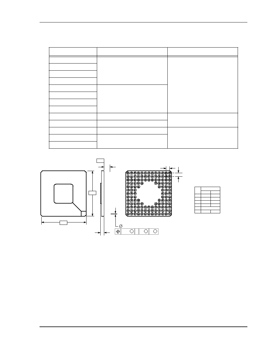
Packaging
Pin-out and Package Information
MOTOROLA
DSP56002/D, Rev. 3
3-31
A8
V
CCQ
Internal Logic
A6
A4
A2
A1
GND
Q
A2
A5
A7
B5
V
CCP
PLL
C6
GND
P
K13
V
CCS
Serial Port
J13
GND
S
L13
Figure 3-9 132-pin Ceramic Pin Grid Array (PGA) Package Mechanical Information
Table 3-12
DSP56002 Power Supply Pins in PGA Package (Continued)
Pin Number
Power Supply
Circuit Supplied
NOTES:
1.
1. DIMENSIONING AND TOLERANCING PER
ANSI Y14.5M, 1982.
2.
2. CONTROLLING DIMENSION: INCH.
DIM
MIN
MAX
INCHES
A
1.340
1.380
B
1.340
1.380
C
0.100
0.150
D
0.017
0.022
G
0.100 BSC
K
0.170
0.195
-A-
-B-
C
K
D
132 PL
-T-
S
A
M
0.005
B
S
T
1 2 3 4 5 6 7 8 9 10 11 12 13
A
B
C
D
E
F
G
H
J
K
L
M
N
G
G
CASE 789B-01
ISSUE O

3-32
DSP56002/D, Rev. 3
MOTOROLA
Packaging
Ordering Drawings
ORDERING DRAWINGS
Complete mechanical information regarding DSP56002 packaging is available by
facsimile through Motorola's MfaxTM system. Call the following number to obtain
information by facsimile:
The Mfax automated system requests the following information:
∑
The receiving facsimile telephone number including area code or country
code
∑
The caller's Personal Identification Number (PIN)
Note:
For first time callers, the system provides instructions for setting up a PIN,
which requires entry of a name and telephone number.
∑
The type of information requested:
≠
Instructions for using the system
≠
A literature order form
≠
Specific part technical information or data sheets
≠
Other information described by the system messages
A total of three documents may be ordered per call.
The DSP56002 132-pin PQFP package mechanical drawing is referenced as 831A-02.
The reference number for the 144-pin TQFP package is 918-03. The reference number
for the 132-pin ceramic PGA package is 789B-01.
(602) 244-6591

MOTOROLA
DSP56002/D, Rev. 3
4-1
SECTION
4
DESIGN CONSIDERATIONS
HEAT DISSIPATION
An estimation of the chip junction temperature, T
J
, in
∞
C can be obtained from the
equation:
Equation 1:
Where:
T
A
= ambient temperature ∞C
R
JA
= package junction-to-ambient thermal resistance ∞C/W
P
D
= power dissipation in package
Historically, thermal resistance has been expressed as the sum of a junction-to-case
thermal resistance and a case-to-ambient thermal resistance:
Equation 2:
Where:
R
JA
= package junction-to-ambient thermal resistance ∞C/W
R
JC
= package junction-to-case thermal resistance ∞C/W
R
CA
= package case-to-ambient thermal resistance ∞C/W
R
JC
is device-related and cannot be influenced by the user. The user controls the
thermal environment to change the case-to-ambient thermal resistance, R
CA
. For
example, the user can change the air flow around the device, add a heat sink, change
the mounting arrangement on the Printed Circuit Board, or otherwise change the
thermal dissipation capability of the area surrounding the device on a Printed Circuit
Board. This model is most useful for ceramic packages with heat sinks; some 90% of
the heat flow is dissipated through the case to the heat sink and out to the ambient
environment. For ceramic packages, in situations where the heat flow is split between
a path to the case and an alternate path through the Printed Circuit Board, analysis of
the device thermal performance may need the additional modeling capability of a
system level thermal simulation tool.
The thermal performance of plastic packages is more dependent on the temperature
of the Printed Circuit Board to which the package is mounted. Again, if the
T
J
T
A
P
D
R
JA
◊
(
)
+
=
R
JA
R
JC
R
CA
+
=

4-2
DSP56002/D, Rev. 3
MOTOROLA
Design Considerations
Heat Dissipation
estimations obtained from R
JA
do not satisfactorily answer whether the thermal
performance is adequate, a system level model may be appropriate.
A complicating factor is the existence of three common ways for determining the
junction-to-case thermal resistance in plastic packages:
∑
To minimize temperature variation across the surface, the thermal resistance
is measured from the junction to the outside surface of the package (case)
closest to the chip mounting area when that surface has a proper heat sink.
∑
To define a value approximately equal to a junction-to-board thermal
resistance, the thermal resistance is measured from the junction to where the
leads are attached to the case.
∑
If the temperature of the package case (T
T
) as determined by a thermocouple,
the thermal resistance is computed using the value obtained by the equation
(T
J
≠ T
T
)/P
D
.
As noted above, the junction-to-case thermal resistances quoted in this data sheet are
determined using the first definition. From a practical standpoint, that value is also
suitable for determining the junction temperature from a case thermocouple reading
in forced convection environments. In natural convection, using the junction-to-case
thermal resistance to estimate junction temperature from a thermocouple reading on
the case of the package will estimate a junction temperature slightly hotter than
actual temperature. Hence, the new thermal metric, Thermal Characterization
Parameter or
JT
, has been defined to be (T
J
≠ T
T
)/P
D
. This value gives a better
estimate of the junction temperature in natural convection when using the surface
temperature of the package. Remember that surface temperature readings of
packages are subject to significant errors caused by inadequate attachment of the
sensor to the surface and to errors caused by heat loss to the sensor. The
recommended technique is to attach a 40-gauge thermocouple wire and bead to the
top center of the package with thermally conductive epoxy.
Note:
Table 2-2 Thermal Characteristics
on page 2-2 contains the package thermal
values for this chip.

Design Considerations
Electrical Design Considerations
MOTOROLA
DSP56002/D, Rev. 3
4-3
ELECTRICAL DESIGN CONSIDERATIONS
Use the following list of recommendations to assure correct DSP operation:
∑
Provide a low-impedance path from the board power supply to each V
CC
pin
on the DSP, and from the board ground to each GND pin.
∑
Use at least four 0.1
µ
F bypass capacitors positioned as close as possible to the
four sides of the package to connect the V
CC
power source to GND.
∑
Ensure that capacitor leads and associated printed circuit traces that connect
to the chip V
CC
and GND pins are less than 0.5 inch per capacitor lead.
∑
Use at least a four-layer Printed Circuit Board (PCB) with two inner layers for
V
CC
and GND.
∑
Because the DSP output signals have fast rise and fall times, PCB trace lengths
should be minimal. This recommendation particularly applies to the address
and data buses as well as the RD, WR, IRQA, IRQB, NMI, HEN, and HACK
pins.
∑
Consider all device loads as well as parasitic capacitance due to PCB traces
when calculating capacitance. This is especially critical in systems with higher
capacitive loads that could create higher transient currents in the V
CC
and
GND circuits.
∑
All inputs must be terminated (i.e., not allowed to float) using CMOS levels.
∑
Take special care to minimize noise levels on the PLL supply pins (both V
CC
and GND).
CAUTION
This device contains protective circuitry to
guard against damage due to high static
voltage or electrical fields. However, normal
precautions are advised to avoid application
of any voltages higher than maximum rated
voltages to this high-impedance circuit.
Reliability of operation is enhanced if unused
inputs are tied to an appropriate logic voltage
level (e.g., either GND or V
CC
).

4-4
DSP56002/D, Rev. 3
MOTOROLA
Design Considerations
Power Consumption
POWER CONSUMPTION
Power dissipation is a key issue in portable DSP applications. The following describes
some factors which affect current consumption. Current consumption is described by
the formula:
Equation 3:
where:
C = node/pin capacitance
V = voltage swing
f = frequency of node/pin toggle
For example, for an address pin loaded with a 50 pF capacitance and operating at 5.5
V with a 40 MHz clock, toggling at its maximum possible rate (which is 10 MHz), the
current consumption is:
Equation 4:
The maximum internal current value (I
CCI
-max), reflects the maximum I
CC
expected
when running the code given below. This represents "typical" internal activity, and is
included as a point of reference. Some applications may consume more or less current
depending on the code used. The typical internal current value (I
CCI
-typ) reflects
what is typically seen when running the given code.
The following steps are recommended for applications requiring very low current
consumption:
1. Minimize external memory accesses; use internal memory accesses instead.
2. Minimize the number of pins that are switching.
3. Minimize the capacitive load on the pins.
4. Connect the unused inputs to pull-up or pull-down resistors.
I
C
V
f
◊
◊
=
I
50
10
12
≠
◊
5.5
◊
10
◊
10
6
◊
2.75mA
=
=

Design Considerations
Power Consumption
MOTOROLA
DSP56002/D, Rev. 3
4-5
Current consumption test code:
org p:RESET
jmp MAIN
org p:MAIN
movep #$180000,x:$FFFD
move #0,r0
move
#0,r4
move
#$00FF, m0
move
#$00FF, m4
nop
rep #256
move
r0,x:(r0)+
rep
#256
mov
r4,y:(r4)+
clr
a
move
l:(r0)+,a
rep
#30
mac
x0,y0,a x:(r0)+,x0 y:(r4)+,y0
move
a,p:(r5)
jmp
TP1
TP1
nop
jmp
MAIN

4-6
DSP56002/D, Rev. 3
MOTOROLA
Design Considerations
Host Port Considerations
HOST PORT CONSIDERATIONS
Careful synchronization is required when reading multibit registers that are written
by another asynchronous system. This is a common problem when two
asynchronous systems are connected. The situation exists in the host interface. The
following paragraphs present considerations for proper operation.
Host Programming Considerations
UNSYNCHRONIZED READING OF RECEIVE BYTE REGISTERS
When reading receive byte registers (RXH, RXM, and RXL) the host programmer
should use interrupts or poll the RXDF flag that indicates that data is available. This
assures that the data in the receive byte registers will be stable.
OVERWRITING TRANSMIT BYTE REGISTERS
The host programmer should not write to the transmit byte registers (TXH, TXM, and
TXL) unless the TXDE bit is set indicating that the transmit byte registers are empty.
This guarantees that the transmit byte registers will transfer valid data to the HRX
register.
SYNCHRONIZATION OF STATUS BITS FROM DSP TO HOST
HC, HREQ, DMA, HF3, HF2, TRDY, TXDE, and RXDF status bits are set or cleared
from inside the DSP and read by the host processor. The host can read these status
bits very quickly without regard to the clock rate used by the DSP, but the possibility
exists that the state of the bit could be changing during the read operation. This is
generally not a system problem, since the bit will be read correctly in the next pass of
any host polling routine.
Note:
Refer to
DSP56002 User's Manual
sections describing the I/O Interface and
Host/DMA Interface Programming Model for descriptions of these status
bits.
OVERWRITING THE HOST VECTOR
The Host programmer should change the Host Vector register only when the Host
Command bit (HC) is clear. This change guarantees that the DSP interrupt control
logic will receive a stable vector.

Design Considerations
Host Port Considerations
MOTOROLA
DSP56002/D, Rev. 3
4-7
CANCELLING A PENDING HOST COMMAND EXCEPTION
The host processor may elect to clear the HC bit to cancel the Host Command
Exception request at any time before it is recognized by the DSP. Because the host
does not know exactly when the exception will be recognized (due to exception
processing synchronization and pipeline delays), the DSP may execute the Host
Command Exception after the HC bit is cleared. For these reasons, the HV bits must
not be changed at the same time the HC bit is cleared.
VARIANCE IN THE HI TIMING
HI timing may vary during initial startup during the time after reset before the PLL
locks. Therefore, before a host attempt to load (i.e., bootstrap) the DSP, the host
should first make sure that the HI port programming has been completed. The
following steps can be used to ensure that the programming is complete:
1. Set the INIT bit in the ICR
2. Poll the INIT bit until it is cleared.
3. Read the ISR.
An alternate method is:
1. Write the TREQ/RREQ together with INIT.
2. Poll INIT, ISR, and the HREQ pin.
DSP Programming Considerations
SYNCHRONIZATION OF STATUS BITS FROM HOST TO DSP
DMA, HF1, HF0, and HCP, HTDE, and HRDF status bits are set or cleared by the host
processor side of the interface. These bits are individually synchronized to the DSP
clock.
Note:
Refer to
DSP56002 User's Manual
sections describing the I/O Interface and
Host/DMA Interface Programming Model for descriptions of these status
bits.
READING HF0 AND HF1 AS AN ENCODED PAIR
A potential problem exists when reading status bits HF0 and HF1 as an encoded pair
(i.e., the four combinations 00, 01, 10, and 11 each have significance). A very small
probability exists that the DSP will read the status bits synchronized during
transition. The solution to this potential problem is to read the HF0 and HF1 bits
twice and check for consensus.

4-8
DSP56002/D, Rev. 3
MOTOROLA
Design Considerations
Package Compatibility
PACKAGE COMPATIBILITY
The PQFP and TQFP packages are designed so that a single Printed Circuit Board
(PCB) can accommodate either package. The two package pinouts are similarly
sequenced. Proper orientation of each package with the smaller TQFP footprint
inside the PQFP footprint allow connection of PCB traces to either package. For
example, the D0 pin is near the corner of both the PQFP package (pin 84) and the
TQFP package (pin 109), and is adjacent to D1 on both packages.
Note:
Some "no connect" pins in the TQFP pin sequence are excluded from the
PQFP pin sequence.

MOTOROLA
DSP56002/D, Rev. 3
5-1
SECTION
5
ORDERING INFORMATION
DSP56002 ordering information in the table below lists the pertinent information
needed to place an order. Consult a Motorola Semiconductor sales office or
authorized distributor to determine availability and to order parts.
Table 5-1
DSP56002 Ordering Information
Part
Supply
Voltage
Package Type
Pin Count
Frequency
(MHz)
Order Number
DSP56002
5 V
Plastic Quad Flat Pack
(PQFP)
132
40
DSP56002FC40
66
DSP56002FC66
80
DSP56002FC80
Plastic Thin Quad Flat
Pack (TQFP)
144
40
DSP56002PV40
66
DSP56002PV66
80
DSP56002PV80
Ceramic Pin Grid Array
132
40
DSP56002RC40
Motorola reserves the right to make changes without further notice to any products herein. Motorola makes no
warranty, representation or guarantee regarding the suitability of its products for any particular purpose, nor does
Motorola assume any liability arising out of the application or use of any product or circuit, and specifically disclaims
any and all liability, including without limitation consequential or incidental damages. "Typical" parameters which may
be provided in Motorola data sheets and/or specifications can and do vary in different applications and actual
performance may vary over time. All operating parameters, including "Typicals" must be validated for each customer
application by customer's technical experts. Motorola does not convey any license under its patent rights nor the rights
of others. Motorola products are not designed, intended, or authorized for use as components in systems intended for
surgical implant into the body, or other applications intended to support life, or for any other application in which the
failure of the Motorola product could create a situation where personal injury or death may occur. Should Buyer
purchase or use Motorola products for any such unintended or unauthorized application, Buyer shall indemnify and
hold Motorola and its officers, employees, subsidiaries, affiliates, and distributors harmless against all claims, costs,
damages, and expenses, and reasonable attorney fees arising out of, directly or indirectly, any claim of personal injury
or death associated with such unintended or unauthorized use, even if such claim alleges that Motorola was negligent
regarding the design or manufacture of the part. Motorola and
are registered trademarks of Motorola, Inc.
Motorola, Inc. is an Equal Opportunity/Affirmative Action Employer.
How to reach us:
USA/Europe/Locations Not Listed
:
Motorola Literature Distribution
P.O. Box 5405
Denver, Colorado 80217
303-675-2140
1 (800) 441-2447
MfaxTM
:
RMFAX0@email.sps.mot.com
TOUCHTONE (602) 244-6609
US & Canada ONLY (800) 774-1848
Asia/Pacific
:
Motorola Semiconductors H.K. Ltd.
8B Tai Ping Industrial Park
51 Ting Kok Road
Tai Po, N.T., Hong Kong
852-26629298
Technical Resource Center:
1 (800) 521-6274
DSP Helpline
dsphelp@dsp.sps.mot.com
Japan
:
Nippon Motorola Ltd.
SPD, Strategic Planning Office
4-32-1, Nishi-Gotanda
Sinagawa-ku, Tokyo 141, Japan
81-3-5487-8488
Internet
:
http://www.motorola-dsp.com
OnCE and Mfax are trademarks of Motorola, Inc.