 | –≠–ª–µ–∫—Ç—Ä–æ–Ω–Ω—ã–π –∫–æ–º–ø–æ–Ω–µ–Ω—Ç: DSP56364D | –°–∫–∞—á–∞—Ç—å:  PDF PDF  ZIP ZIP |

This document contains information on a new product. Specifications and information herein are subject to change without notice.
IMOTOROLA
DSP56364 Advance Information
1
Overview
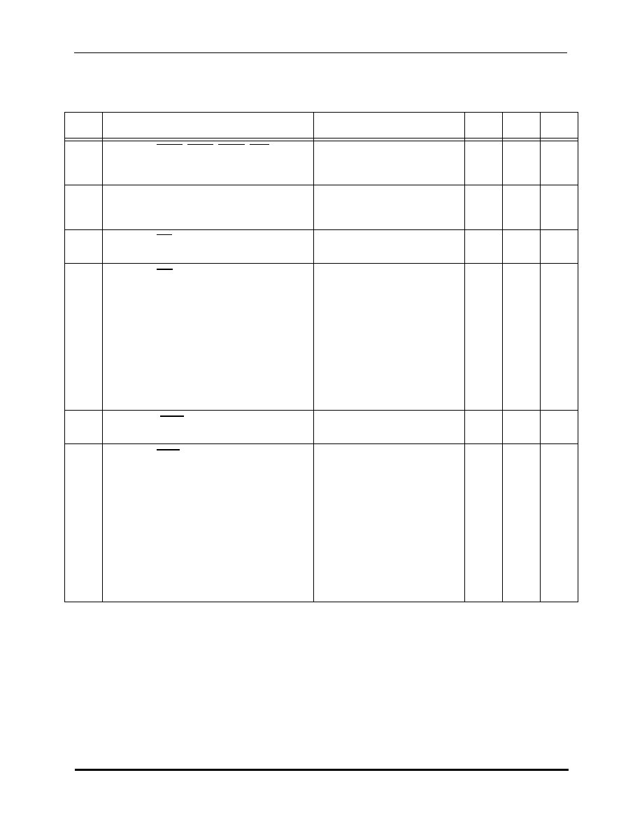
The DSP56364 supports digital audio applications requiring sound field processing,
acoustic equalization, and other digital audio algorithms. The DSP56364 uses the
high performance, single-clock-per-cycle DSP56300 core family of programmable
CMOS digital signal processors (DSPs) combined with the audio signal processing
capability of the Motorola SymphonyTM DSP family, as shown in
Figure 1
. This
design provides a two-fold performance increase over Motorola's popular
Symphony family of DSPs while retaining code compatibility. Significant
architectural enhancements include a barrel shifter, 24-bit addressing, instruction
cache, and direct memory access (DMA). The DSP56364 offers 100 million
instructions per second (MIPS) using an internal 100 MHz clock at 3.3 V.
Data Sheet Conventions
This data sheet uses the following conventions:
OVERBAR
Used to indicate a signal that is active when pulled low (For
example, the RESET pin is active when low.)
"asserted"
Means that a high true (active high) signal is high or that a low
true (active low) signal is low
"deasserted"
Means that a high true (active high) signal is low or that a low
true (active low) signal is high
Examples:
Signal/
Symbol
Logic State
Signal State
Voltage*
PIN
True
Asserted
V
IL
/ V
OL
PIN
False
Deasserted
V
IH
/ V
OH
PIN
True
Asserted
V
IH
/ V
OH
PIN
False
Deasserted
V
IL
/ V
OL
Note: *Values for V
IL
, V
OL
, V
IH
, and V
OH
are defined by individual product
specifications.
Advance Information
DSP56364/D
Rev. 3.2, 08/2003
24-Bit Audio Digital
Signal Processor
Topic
Page
Overview ..................................... i
Features .................................... ii
Signal/Connection
Descriptions .......................1-1
Specifications ..........................2-1
Packaging ...............................3-1
Design Considerations ...........4-1
Ordering Information ...............5-1
IBIS Model ............................. A-1
F
r
e
e
s
c
a
l
e
S
e
m
i
c
o
n
d
u
c
t
o
r
,
I
Freescale Semiconductor, Inc.
For More Information On This Product,
Go to: www.freescale.com
n
c
.
.
.

Overview
Features
2
DSP56364 Advance Information
MOTOROLA
Figure 1 DSP56364 Block Diagram
1
Features
1.1
Digital Signal Processing Core
∑
100 Million Instructions Per Second (MIPS) with an 100 MHz clock at 3.3V.
∑
Object Code Compatible with the 56000 core.
∑
Data ALU with a 24 x 24 bit multiplier-accumulator and a 56-bit barrel shifter. 16-bit arithmetic support.
∑
Program Control with position independent code support and instruction cache support.
∑
Six-channel DMA controller.
∑
PLL based clocking with a wide range of frequency multiplications (1 to 4096), predivider factors (1
to 16) and power saving clock divider (2
i
: i=0 to 7). Reduces clock noise.
∑
Internal address tracing support and OnCE
for Hardware/Software debugging.
CLOCK
INTERNAL
DATA BUS
SWITCH
EXTAL
PROGRAM RAM
0.5K x 24
PROGRAM ROM
8K x 24
Bootstrap ROM
192 x 24
PROGRAM
INTERRUPT
CONT
PROGRAM
DECODE
CONT
PROGRAM
ADDRESS
GEN
YAB
XAB
PAB
YDB
XDB
PDB
GDB
MODA/IRQA
MODB/IRQB
DATA ALU
24 X 24+56
56-BIT MAC
TWO 56-BIT
ACCUMULATORS
BARREL SHIFTER
MODD/IRQD
PLL
ADDRESS
GENERATION UNIT
OnCE
TM
DSP56300
GPIO
ESAI
12
4
24-BIT
X
MEMORY
RAM
1K X 24
Y
MEMORY
RAM
1.5K X 24
DDB
DAB
SIX CHANNELS
DMA UNIT
CORE
YM
_
E
B
XM
_
E
B
PM
_
EB
PIO
_
E
B
24 BITS BUS
SHI
JTAG
4
5
RESET
POWER
MGMT
PINIT/NMI
DRAM & SRAM
BUS
INTERFACE
EXTERNAL
ADDRESS BUS
SWITCH
EXTERNAL
DATA BUS
SWITCH
ADDRESS
6
DATA
CONTROL
8
18
PERIPHERAL
EXPANSION
AREA
MEMORY
EXPANSION
AREA
F
r
e
e
s
c
a
l
e
S
e
m
i
c
o
n
d
u
c
t
o
r
,
I
Freescale Semiconductor, Inc.
For More Information On This Product,
Go to: www.freescale.com
n
c
.
.
.

Overview
Documentation
MOTOROLA
DSP56364 Advance Information
3
∑
JTAG port.
∑
Very low-power CMOS design, fully static design with operating frequencies down to DC.
∑
STOP and WAIT low-power standby modes.
1.2
On-chip Memory Configuration
∑
1.5Kx24 Bit Y-Data RAM.
∑
1Kx24 Bit X-Data RAM.
∑
8Kx24 Bit Program ROM.
∑
0.5Kx24 Bit Program RAM and 192x24 Bit Bootstrap ROM.
∑
0.75Kx24 Bit from Y Data RAM can be switched to Program RAM resulting in up to 1.25Kx24 Bit of
Program RAM.
1.3
Off-chip memory expansion
∑
External Memory Expansion Port with 8-bit data bus.
∑
Off-chip expansion up to 2 x 16M x 8-bit word of Data/Program memory when using DRAM.
∑
Off-chip expansion up to 2 x 256k x 8-bit word of Data/Program memory when using SRAM.
∑
Simultaneous glueless interface to SRAM and DRAM.
1.4
Peripheral modules
∑
Enhanced Serial Audio Interface (ESAI): 6 serial lines, 4 selectable as receive or transmitt and 2
transmitt only, master or slave. I
2
S, Sony, AC97, network and other programmable protocols.
Unused pins of ESAI may be used as GPIO lines.
∑
Serial Host Interface (SHI): SPI and I
2
C protocols, 10-word receive FIFO, support for 8, 16 and
24-bit words.
∑
Four dedicated GPIO lines.
1.5
Packaging
∑
100-pin plastic TQFP package.
2
Documentation
Table 1
lists the documents that provide a complete description of the DSP56364 and are required to
design properly with the part. Documentation is available from a local Motorola distributor, a Motorola
semiconductor sales office, a Motorola Literature Distribution Center, or through the Motorola DSP home
page on the Internet (the source for the latest information).
F
r
e
e
s
c
a
l
e
S
e
m
i
c
o
n
d
u
c
t
o
r
,
I
Freescale Semiconductor, Inc.
For More Information On This Product,
Go to: www.freescale.com
n
c
.
.
.

Overview
Documentation
4
DSP56364 Advance Information
MOTOROLA
Table 1 DSP56364 Documentation
Document Name
Description
Order Number
DSP56300 Family Manual
Detailed description of the 56000-family
architecture and the 24-bit core processor
and instruction set
DSP56300FM/AD
DSP56364 User's Manual
Detailed description of memory, peripher-
als, and interfaces
DSP56364UM/AD
DSP56364 Technical Data Sheet
Electrical and timing specifications; pin
and package descriptions
DSP56364/D
There is also a product brief for this chip.
DSP56364 Product Brief
Brief description of the chip
DSP56364P/D
F
r
e
e
s
c
a
l
e
S
e
m
i
c
o
n
d
u
c
t
o
r
,
I
Freescale Semiconductor, Inc.
For More Information On This Product,
Go to: www.freescale.com
n
c
.
.
.

MOTOROLA
DSP56364 Advance Information
1-1
SECTION 1
SIGNAL/CONNECTION DESCRIPTIONS
1.1
SIGNAL GROUPINGS
The input and output signals of the DSP56364 are organized into functional groups, which are listed in
Table 1-1
and illustrated in
Figure 1-1
.
The DSP56364 is operated from a 3.3 V supply; however, some of the inputs can tolerate 5 V. A special
notice for this feature is added to the signal descriptions of those inputs.
Table 1-1 DSP56364 Functional Signal Groupings
Functional Group
Number of
Signals
Detailed
Description
Power (V
CC
)
18
Table 1-2
Ground (GND)
14
Table 1-3
Clock and PLL
3
Table 1-4
Address bus
Port A
1
18
Table 1-5
Data bus
8
Table 1-6
Bus control
6
Table 1-7
Interrupt and mode control
4
Table 1-8
General Purpose I/O
Port B2
4
Table 1-12
SHI
5
Table 1-9
ESAI
Port C3
12
Table 1-10
JTAG/OnCE Port
4
Table 1-11
Notes:
1.
Port A is the external memory interface port, including the external address bus, data bus, and control
signals.
2.
Port B signals are the GPIO signals.
3.
Port C signals are the ESAI port signals multiplexed with the GPIO signals.
F
r
e
e
s
c
a
l
e
S
e
m
i
c
o
n
d
u
c
t
o
r
,
I
Freescale Semiconductor, Inc.
For More Information On This Product,
Go to: www.freescale.com
n
c
.
.
.

Signal/Connection Descriptions
Signal Groupings
1-2
DSP56364 Advance Information
MOTOROLA
Figure 1-1 Signals Identified by Functional Group
PORT A ADDRESS BUS
A0-A17
VCCA (4)
GNDA (4)
D0-D7
VCCD (1)
GNDD (1)
AA0-AA1/RAS0-RAS1
RD
WR
TA
RESERVED (4)
VCCC (1)
GNDC (1)
PORT A BUS CONTROL
PORT A DATA BUS
OnCE
ON-CHIP EMULATION/
TDI
TCK
TDO
GPIO
PB0-PB3
SERIAL AUDIO INTERFACE (ESAI)
SCKT [PC3]
FST [PC4]
HCKT [PC5]
SERIAL HOST INTERFACE (SHI)
MOSI/HA0
SS
/HA2
MISO/SDA
SCK/SCL
INTERRUPT AND
MODE CONTROL
MODB/IRQB
MODD/IRQD
RESET
QUIET POWER
EXTAL
VCCLQ (4)
GNDQ (4)
PLL AND CLOCK
GNDP
VCCP
PCAP
DSP56364
Port B
Port C
JTAG PORT
TMS
MODA/IRQA
PINIT/NMI
VCCSS (3)
GNDS (3)
CAS
VCCHQ (4)
HREQ
SCKR [PC0]
FSR [PC1]
HCKR [PC2]
SDO0 [PC11]
SDO1 [PC10]
SDO2/SDI3 [PC9]
SDO3/SDI2 [PC8]
SDO4/SDI1 [PC7]
SDO5/SDI0 [PC6]
F
r
e
e
s
c
a
l
e
S
e
m
i
c
o
n
d
u
c
t
o
r
,
I
Freescale Semiconductor, Inc.
For More Information On This Product,
Go to: www.freescale.com
n
c
.
.
.

Signal/Connection Descriptions
Power
MOTOROLA
DSP56364 Advance Information
1-3
1.2
POWER
Table 1-2 Power Inputs
Power Name
Description
V
CCP
PLL Power--V
CCP
is V
CC
dedicated for PLL use. The voltage should be well-regulated
and the input should be provided with an extremely low impedance path to the V
CC
power rail. There is one V
CCP
input.
V
CCQL
(4)
Quiet Core (Low) Power--V
CCQL
is an isolated power for the internal processing logic.
This input must be tied externally to all other chip power inputs. The user must provide
adequate external decoupling capacitors. There are four V
CCQL
inputs.
V
CCQH
(4)
Quiet External (High) Power--V
CCQH
is a quiet power source for I/O lines. This input
must be tied externally to all other chip power inputs. The user must provide adequate
decoupling capacitors. There are four V
CCQH
inputs.
V
CCA
(4)
Address Bus Power--V
CCA
is an isolated power for sections of the address bus
I/O drivers. This input must be tied externally to all other chip power inputs. The user
must provide adequate external decoupling capacitors. There are four V
CCA
inputs.
V
CCD
(1)
Data Bus Power--V
CCD
is an isolated power for sections of the data bus I/O drivers.
This input must be tied externally to all other chip power inputs. The user must provide
adequate external decoupling capacitors. There is one V
CCD
inputs.
V
CCC
(1)
Bus Control Power--V
CCC
is an isolated power for the bus control I/O drivers. This
input must be tied externally to all other chip power inputs. The user must provide ade-
quate external decoupling capacitors. There is one V
CCC
inputs.
V
CCS
(3)
SHI and ESAI --V
CCS
is an isolated power for the SHI and ESAI. This input must be
tied externally to all other chip power inputs
L
. The user must provide adequate external
decoupling capacitors. There are three V
CCS
inputs.
F
r
e
e
s
c
a
l
e
S
e
m
i
c
o
n
d
u
c
t
o
r
,
I
Freescale Semiconductor, Inc.
For More Information On This Product,
Go to: www.freescale.com
n
c
.
.
.

Signal/Connection Descriptions
Ground
1-4
DSP56364 Advance Information
MOTOROLA
1.3
GROUND
Table 1-3 Grounds
Ground
Name
Description
GND
P
PLL Ground--GND
P
is ground-dedicated for PLL use. The connection should be pro-
vided with an extremely low-impedance path to ground. V
CCP
should be bypassed to
GND
P
by a 0.47
µ
F capacitor located as close as possible to the chip package. There is
one GND
P
connection.
GND
Q
(4)
Quiet Ground--GND
Q
is an isolated ground for the internal processing logic. This con-
nection must be tied externally to all other chip ground connections. The user must pro-
vide adequate external decoupling capacitors. There are four GND
Q
connections.
GND
A
(4)
Address Bus Ground--GND
A
is an isolated ground for sections of the address bus
I/O drivers. This connection must be tied externally to all other chip ground connec-
tions. The user must provide adequate external decoupling capacitors. There are four
GND
A
connections.
GND
D
(1)
Data Bus Ground--GND
D
is an isolated ground for sections of the data bus
I/O drivers. This connection must be tied externally to all other chip ground connec-
tions. The user must provide adequate external decoupling capacitors. There is one
GND
D
connections.
GND
C
(1)
Bus Control Ground--GND
C
is an isolated ground for the bus control I/O drivers. This
connection must be tied externally to all other chip ground connections. The user must
provide adequate external decoupling capacitors. There is one GND
C
connections.
GND
S
(3)
SHI and ESAI --GND
S
is an isolated ground for the SHI and ESAI. This connection
must be tied externally to all other chip ground connections. The user must provide
adequate external decoupling capacitors. There are three GND
S
connections.
F
r
e
e
s
c
a
l
e
S
e
m
i
c
o
n
d
u
c
t
o
r
,
I
Freescale Semiconductor, Inc.
For More Information On This Product,
Go to: www.freescale.com
n
c
.
.
.

Signal/Connection Descriptions
Clock and PLL
MOTOROLA
DSP56364 Advance Information
1-5
1.4
CLOCK AND PLL
Table 1-4 Clock and PLL Signals
Signal
Name
Type
State
during
Reset
Signal Description
EXTAL
Input
Input
External Clock Input--An external clock source must be connected
to EXTAL in order to supply the clock to the internal clock generator
and PLL.
PCAP
Input
Input
PLL Capacitor--PCAP is an input connecting an off-chip capacitor
to the PLL filter. Connect one capacitor terminal to PCAP and the
other terminal to V
CCP
.
If the PLL is not used, PCAP may be tied to V
CC
, GND, or left float-
ing.
PINIT/NMI
Input
Input
PLL Initial/Nonmaskable Interrupt--During assertion of RESET,
the value of PINIT/NMI is written into the PLL Enable (PEN) bit of the
PLL control register, determining whether the PLL is enabled or dis-
abled. After RESET de assertion and during normal instruction pro-
cessing, the PINIT/NMI Schmitt-trigger input is a
negative-edge-triggered nonmaskable interrupt (NMI) request inter-
nally synchronized to internal system clock.
This input is 5 V tolerant.
F
r
e
e
s
c
a
l
e
S
e
m
i
c
o
n
d
u
c
t
o
r
,
I
Freescale Semiconductor, Inc.
For More Information On This Product,
Go to: www.freescale.com
n
c
.
.
.

Signal/Connection Descriptions
External Memory Expansion Port (Port A)
1-6
DSP56364 Advance Information
MOTOROLA
1.5
EXTERNAL MEMORY EXPANSION PORT (PORT A)
When the DSP56364 enters a low-power standby mode (stop or wait), it tri-states the relevant port A
signals: D0≠D7, AA0, AA1, RD, WR, CAS.
1.5.1
External Address Bus
1.5.2
External Data Bus
Table 1-5 External Address Bus Signals
Signal Name
Type
State during
Reset
Signal Description
A0≠A17
Output
Keeper
active
Address Bus--A0≠A17 are active-high outputs that spec-
ify the address for external program and data memory
accesses. Otherwise, the signals are kept to their previous
values by internal weak keepers. To minimize power dissi-
pation, A0≠A17 do not change state when external mem-
ory spaces are not being accessed.
Table 1-6 External Data Bus Signals
Signal Name
Type
State during
Reset
Signal Description
D0≠D7
Input/
Output
Tri-stated
Data Bus--D0≠D7 are active-high, bidirectional input/out-
puts that provide the bidirectional data bus for external
program and data memory accesses. D0≠D7 are tri-stated
during hardware reset and when the DSP is in the stop or
wait low-power standby mode.
F
r
e
e
s
c
a
l
e
S
e
m
i
c
o
n
d
u
c
t
o
r
,
I
Freescale Semiconductor, Inc.
For More Information On This Product,
Go to: www.freescale.com
n
c
.
.
.

Signal/Connection Descriptions
External Memory Expansion Port (Port A)
MOTOROLA
DSP56364 Advance Information
1-7
1.5.3
External Bus Control
Table 1-7 External Bus Control Signals
Signal Name
Type
State
during
Reset
Signal Description
AA0≠AA1/
RAS0
≠
RAS1
Output
Tri-stated
Address Attribute or Row Address Strobe--When defined as AA, these
signals can be used as chip selects or additional address lines. When
defined as
RAS
, these signals can be used as
RAS
for DRAM interface.
These signals are tri-statable outputs with programmable polarity. These
signals are tri-stated during hardware reset and when the DSP is in the
stop or wait low-power standby mode.
CAS
Output
Tri-stated
Column Address Strobe--
CAS
is an active-low output used by DRAM
to strobe the column address. This signal is tri-stated during hardware
reset and when the DSP is in the stop or wait low-power standby mode.
RD
Output
Tri-stated
Read Enable--
RD
is an active-low output that is asserted to read exter-
nal memory on the data bus. This signal is tri-stated during hardware reset
and when the DSP is in the stop or wait low-power standby mode.
WR
Output
Tri-stated
Write Enable--
WR
is an active-low output that is asserted to write exter-
nal memory on the data bus. This signal is tri-stated during hardware reset
and when the DSP is in the stop or wait low-power standby mode.
TA
Input
Ignored
Input
Transfer Acknowledge--If there is no external bus activity, the
TA
input
is ignored. The
TA
input is a data transfer acknowledge (DTACK) function
that can extend an external bus cycle indefinitely. Any number of wait
states (1, 2. . .infinity) may be added to the wait states inserted by the
BCR by keeping
TA
deasserted. In typical operation,
TA
is deasserted at
the start of a bus cycle, is asserted to enable completion of the bus cycle,
and is deasserted before the next bus cycle. The current bus cycle com-
pletes one clock period after
TA
is asserted synchronous to the internal
system clock. The number of wait states is determined by the
TA
input or
by the bus control register (BCR), whichever is longer. The BCR can be
used to set the minimum number of wait states in external bus cycles.
In order to use the TA functionality, the BCR must be programmed to at
least one wait state. A zero wait state access cannot be extended by TA
deassertion, otherwise improper operation may result.
TA
can operate
synchronously or asynchronously, depending on the setting of the TAS bit
in the operating mode register (OMR).
TA
functionality may not be used while performing DRAM type accesses,
otherwise improper operation may result.
F
r
e
e
s
c
a
l
e
S
e
m
i
c
o
n
d
u
c
t
o
r
,
I
Freescale Semiconductor, Inc.
For More Information On This Product,
Go to: www.freescale.com
n
c
.
.
.

Signal/Connection Descriptions
Interrupt and Mode Control
1-8
DSP56364 Advance Information
MOTOROLA
1.6
INTERRUPT AND MODE CONTROL
The interrupt and mode control signals select the chip's operating mode as it comes out of hardware reset.
After RESET is deasserted, these inputs are hardware interrupt request lines.
Table 1-8 Interrupt and Mode Control
Signal Name
Type
State
during
Reset
Signal Description
MODA/
IRQA
Input
Input
Mode Select A/External Interrupt Request A--MODA/
IRQA
is an active-low
Schmitt-trigger input, internally synchronized to the internal system clock.
MODA/
IRQA
selects the initial chip operating mode during hardware reset and
becomes a level-sensitive or negative-edge-triggered, maskable interrupt
request input during normal instruction processing. MODA, MODB, and MODD
select one of 8 initial chip operating modes, latched into the OMR when the
RESET
signal is deasserted. If
IRQA
is asserted synchronous to the internal
system clock, multiple processors can be re synchronized using the WAIT
instruction and asserting
IRQA
to exit the wait state. If the processor is in the
stop standby state and
IRQA
is asserted, the processor will exit the stop state.
This input is 5 V tolerant.
MODB/
IRQB
Input
Input
Mode Select B/External Interrupt Request B--MODB/
IRQB
is an active-low
Schmitt-trigger input, internally synchronized to the internal system clock.
MODB/
IRQB
selects the initial chip operating mode during hardware reset and
becomes a level-sensitive or negative-edge-triggered, maskable interrupt
request input during normal instruction processing. MODA, MODB, and MODD
select one of 8 initial chip operating modes, latched into OMR when the
RESET
signal is deasserted. If
IRQB
is asserted synchronous to the internal system
clock, multiple processors can be re-synchronized using the WAIT instruction
and asserting
IRQB
to exit the wait state.
This input is 5 V tolerant.
MODD/
IRQD
Input
Input
Mode Select D/External Interrupt Request D--MODD/
IRQD
is an active-low
Schmitt-trigger input, internally synchronized to the internal system clock.
MODD/
IRQD
selects the initial chip operating mode during hardware reset and
becomes a level-sensitive or negative-edge-triggered, maskable interrupt
request input during normal instruction processing. MODA, MODB, and MODD
select one of 8 initial chip operating modes, latched into OMR when the
RESET
signal is deasserted. If
IRQD
is asserted synchronous to the internal system
clock, multiple processors can be re synchronized using the WAIT instruction
and asserting
IRQD
to exit the wait state.
This input is 5 V tolerant.
RESET
Input
Input
Reset--
RESET
is an active-low, Schmitt-trigger input. When asserted, the chip
is placed in the reset state and the internal phase generator is reset. The
Schmitt-trigger input allows a slowly rising input (such as a capacitor charging)
to reset the chip reliably. When the
RESET
signal is deasserted, the initial chip
operating mode is latched from the MODA, MODB, and MODD inputs. The
RESET
signal must be asserted during power up. A stable EXTAL signal must
be supplied before deassertionof
RESET
.
This input is 5 V tolerant.
F
r
e
e
s
c
a
l
e
S
e
m
i
c
o
n
d
u
c
t
o
r
,
I
Freescale Semiconductor, Inc.
For More Information On This Product,
Go to: www.freescale.com
n
c
.
.
.

Signal/Connection Descriptions
Serial Host Interface
MOTOROLA
DSP56364 Advance Information
1-9
1.7
SERIAL HOST INTERFACE
The SHI has five I/O signals that can be configured to allow the SHI to operate in either SPI or I
2
C mode.
Table 1-9 Serial Host Interface Signals
Signal
Name
Signal
Type
State during
Reset
Signal Description
SCK
Input or
output
Tri-stated
SPI Serial Clock--The SCK signal is an output when the SPI is configured as
a master and a Schmitt-trigger input when the SPI is configured as a slave.
When the SPI is configured as a master, the SCK signal is derived from the
internal SHI clock generator. When the SPI is configured as a slave, the SCK
signal is an input, and the clock signal from the external master synchronizes
the data transfer. The SCK signal is ignored by the SPI if it is defined as a
slave and the slave select (SS) signal is not asserted. In both the master and
slave SPI devices, data is shifted on one edge of the SCK signal and is sam-
pled on the opposite edge where data is stable. Edge polarity is determined by
the SPI transfer protocol.
SCL
Input or
output
Tri-stated
I
2
C Serial Clock--SCL carries the clock for I
2
C bus transactions in the I
2
C
mode. SCL is a Schmitt-trigger input when configured as a slave and an
open-drain output when configured as a master. SCL should be connected to
V
CC
through a pull-up resistor.
This signal is tri-stated during hardware, software, and individual reset. Thus,
there is no need for an external pull-up in this state.
This input is 5 V tolerant.
MISO
Input or
output
Tri-stated
SPI Master-In-Slave-Out--When the SPI is configured as a master, MISO is
the master data input line. The MISO signal is used in conjunction with the
MOSI signal for transmitting and receiving serial data. This signal is a
Schmitt-trigger input when configured for the SPI Master mode, an output
when configured for the SPI Slave mode, and tri-stated if configured for the
SPI Slave mode when SS is deasserted. An external pull-up resistor is not
required for SPI operation.
SDA
Input or
open-drain
output
Tri-stated
I
2
C Data and Acknowledge--In I
2
C mode, SDA is a Schmitt-trigger input
when receiving and an open-drain output when transmitting. SDA should be
connected to V
CC
through a pull-up resistor. SDA carries the data for I
2
C
transactions. The data in SDA must be stable during the high period of SCL.
The data in SDA is only allowed to change when SCL is low. When the bus is
free, SDA is high. The SDA line is only allowed to change during the time SCL
is high in the case of start and stop events. A high-to-low transition of the SDA
line while SCL is high is a unique situation, and is defined as the start event. A
low-to-high transition of SDA while SCL is high is a unique situation defined as
the stop event.
This signal is tri-stated during hardware, software, and individual reset. Thus,
there is no need for an external pull-up in this state.
This input is 5 V tolerant.
F
r
e
e
s
c
a
l
e
S
e
m
i
c
o
n
d
u
c
t
o
r
,
I
Freescale Semiconductor, Inc.
For More Information On This Product,
Go to: www.freescale.com
n
c
.
.
.

Signal/Connection Descriptions
Serial Host Interface
1-10
DSP56364 Advance Information
MOTOROLA
MOSI
Input or
output
Tri-stated
SPI Master-Out-Slave-In--When the SPI is configured as a master, MOSI is
the master data output line. The MOSI signal is used in conjunction with the
MISO signal for transmitting and receiving serial data. MOSI is the slave data
input line when the SPI is configured as a slave. This signal is a Schmitt-trig-
ger input when configured for the SPI Slave mode.
HA0
Input
Tri-stated
I
2
C Slave Address 0--This signal uses a Schmitt-trigger input when config-
ured for the I
2
C mode. When configured for I
2
C slave mode, the HA0 signal is
used to form the slave device address. HA0 is ignored when configured for the
I
2
C master mode.
This signal is tri-stated during hardware, software, and individual reset. Thus,
there is no need for an external pull-up in this state.
This input is 5 V tolerant.
SS
Input
Input
SPI Slave Select--This signal is an active low Schmitt-trigger input when
configured for the SPI mode. When configured for the SPI Slave mode, this
signal is used to enable the SPI slave for transfer. When configured for the
SPI master mode, this signal should be kept deasserted (pulled high). If it is
asserted while configured as SPI master, a bus error condition is flagged. If
SS is deasserted, the SHI ignores SCK clocks and keeps the MISO output
signal in the high-impedance state.
HA2
Input
Input
I
2
C Slave Address 2--This signal uses a Schmitt-trigger input when config-
ured for the I
2
C mode. When configured for the I
2
C Slave mode, the HA2 sig-
nal is used to form the slave device address. HA2 is ignored in the I
2
C master
mode.
This signal is tri-stated during hardware, software, and individual reset. Thus,
there is no need for an external pull-up in this state.
This input is 5 V tolerant.
HREQ
Input or
Output
Tri-stated
Host Request--This signal is an active low Schmitt-trigger input when config-
ured for the master mode but an active low output when configured for the
slave mode.
When configured for the slave mode, HREQ is asserted to indicate that the
SHI is ready for the next data word transfer and deasserted at the first clock
pulse of the new data word transfer. When configured for the master mode,
HREQ is an input. When asserted by the external slave device, it will trigger
the start of the data word transfer by the master. After finishing the data word
transfer, the master will await the next assertion of HREQ to proceed to the
next transfer.
This signal is tri-stated during hardware, software, personal reset, or when the
HREQ1≠HREQ0 bits in the HCSR are cleared. There is no need for external
pull-up in this state.
This input is 5 V tolerant.
Table 1-9 Serial Host Interface Signals (continued)
Signal
Name
Signal
Type
State during
Reset
Signal Description
F
r
e
e
s
c
a
l
e
S
e
m
i
c
o
n
d
u
c
t
o
r
,
I
Freescale Semiconductor, Inc.
For More Information On This Product,
Go to: www.freescale.com
n
c
.
.
.

Signal/Connection Descriptions
Enhanced Serial Audio Interface
MOTOROLA
DSP56364 Advance Information
1-11
1.8
ENHANCED SERIAL AUDIO INTERFACE
Table 1-10 Enhanced Serial Audio Interface Signals
Signal
Name
Signal Type
State during
Reset
Signal Description
HCKR
Input or output
GPIO
disconnected
High Frequency Clock for Receiver--When programmed as an
input, this signal provides a high frequency clock source for the
ESAI receiver as an alternate to the DSP core clock. When pro-
grammed as an output, this signal can serve as a high-frequency
sample clock (e.g., for external digital to analog converters [DACs])
or as an additional system clock.
PC2
Input, output,
or
disconnected
GPIO
disconnected
Port C 2--When the ESAI is configured as GPIO, this signal is indi-
vidually programmable as input, output, or internally disconnected.
The default state after reset is GPIO disconnected.
This input is 5 V tolerant.
HCKT
Input or output
GPIO
disconnected
High Frequency Clock for Transmitter--When programmed as
an input, this signal provides a high frequency clock source for the
ESAI transmitter as an alternate to the DSP core clock. When pro-
grammed as an output, this signal can serve as a high frequency
sample clock (e.g., for external DACs) or as an additional system
clock.
PC5
Input, output,
or
disconnected
GPIO
disconnected
Port C 5--When the ESAI is configured as GPIO, this signal is indi-
vidually programmable as input, output, or internally disconnected.
The default state after reset is GPIO disconnected.
This input is 5 V tolerant.
FSR
Input or output
GPIO
disconnected
Frame Sync for Receiver--This is the receiver frame sync
input/output signal. In the asynchronous mode (SYN=0), the FSR
pin operates as the frame sync input or output used by all the
enabled receivers. In the synchronous mode (SYN=1), it operates
as either the serial flag 1 pin (TEBE=0), or as the transmitter exter-
nal buffer enable control (TEBE=1, RFSD=1).
When this pin is configured as serial flag pin, its direction is deter-
mined by the RFSD bit in the RCCR register. When configured as
the output flag OF1, this pin will reflect the value of the OF1 bit in
the SAICR register, and the data in the OF1 bit will show up at the
pin synchronized to the frame sync in normal mode or the slot in
network mode. When configured as the input flag IF1, the data
value at the pin will be stored in the IF1 bit in the SAISR register,
synchronized by the frame sync in normal mode or the slot in net-
work mode.
PC1
Input, output,
or
disconnected
GPIO
disconnected
Port C 1--When the ESAI is configured as GPIO, this signal is indi-
vidually programmable as input, output, or internally disconnected.
The default state after reset is GPIO disconnected.
This input is 5 V tolerant.
F
r
e
e
s
c
a
l
e
S
e
m
i
c
o
n
d
u
c
t
o
r
,
I
Freescale Semiconductor, Inc.
For More Information On This Product,
Go to: www.freescale.com
n
c
.
.
.

Signal/Connection Descriptions
Enhanced Serial Audio Interface
1-12
DSP56364 Advance Information
MOTOROLA
FST
Input or output
GPIO
disconnected
Frame Sync for Transmitter--This is the transmitter frame sync
input/output signal. For synchronous mode, this signal is the frame
sync for both transmitters and receivers. For asynchronous mode,
FST is the frame sync for the transmitters only. The direction is
determined by the transmitter frame sync direction (TFSD) bit in the
ESAI transmit clock control register (TCCR).
PC4
Input, output,
or
disconnected
GPIO
disconnected
Port C 4--When the ESAI is configured as GPIO, this signal is indi-
vidually programmable as input, output, or internally disconnected.
The default state after reset is GPIO disconnected.
This input is 5 V tolerant.
SCKR
Input or output
GPIO
disconnected
Receiver Serial Clock--SCKR provides the receiver serial bit clock
for the ESAI. The SCKR operates as a clock input or output used by
all the enabled receivers in the asynchronous mode (SYN=0), or as
serial flag 0 pin in the synchronous mode (SYN=1).
When this pin is configured as serial flag pin, its direction is determined
by the RCKD bit in the RCCR register. When configured as the output
flag OF0, this pin will reflect the value of the OF0 bit in the SAICR regis-
ter, and the data in the OF0 bit will show up at the pin synchronized to
the frame sync in normal mode or the slot in network mode. When con-
figured as the input flag IF0, the data value at the pin will be stored in
the IF0 bit in the SAISR register, synchronized by the frame sync in nor-
mal mode or the slot in network mode.
PC0
Input, output,
or
disconnected
GPIO
disconnected
Port C 0--When the ESAI is configured as GPIO, this signal is indi-
vidually programmable as input, output, or internally disconnected.
The default state after reset is GPIO disconnected.
This input is 5 V tolerant.
SCKT
Input or output
GPIO
disconnected
Transmitter Serial Clock--This signal provides the serial bit rate
clock for the ESAI. SCKT is a clock input or output used by all
enabled transmitters and receivers in synchronous mode, or by all
enabled transmitters in asynchronous mode.
PC3
Input, output,
or
disconnected
GPIO
disconnected
Port C 3--When the ESAI is configured as GPIO, this signal is indi-
vidually programmable as input, output, or internally disconnected.
The default state after reset is GPIO disconnected.
This input is 5 V tolerant.
Table 1-10 Enhanced Serial Audio Interface Signals (continued)
Signal
Name
Signal Type
State during
Reset
Signal Description
F
r
e
e
s
c
a
l
e
S
e
m
i
c
o
n
d
u
c
t
o
r
,
I
Freescale Semiconductor, Inc.
For More Information On This Product,
Go to: www.freescale.com
n
c
.
.
.

Signal/Connection Descriptions
Enhanced Serial Audio Interface
MOTOROLA
DSP56364 Advance Information
1-13
SDO5
Output
GPIO
disconnected
Serial Data Output 5--When programmed as a transmitter, SDO5
is used to transmit data from the TX5 serial transmit shift register.
SDI0
Input
GPIO
disconnected
Serial Data Input 0--When programmed as a receiver, SDI0 is
used to receive serial data into the RX0 serial receive shift register.
PC6
Input, output,
or
disconnected
GPIO
disconnected
Port C 6--When the ESAI is configured as GPIO, this signal is indi-
vidually programmable as input, output, or internally disconnected.
The default state after reset is GPIO disconnected.
This input is 5 V tolerant.
SDO4
Output
GPIO
disconnected
Serial Data Output 4--When programmed as a transmitter, SDO4
is used to transmit data from the TX4 serial transmit shift register.
SDI1
Input
GPIO
disconnected
Serial Data Input 1--When programmed as a receiver, SDI1 is
used to receive serial data into the RX1 serial receive shift register.
PC7
Input, output,
or
disconnected
GPIO
disconnected
Port C 7--When the ESAI is configured as GPIO, this signal is indi-
vidually programmable as input, output, or internally disconnected.
The default state after reset is GPIO disconnected.
This input is 5 V tolerant.
SDO3
Output
GPIO
disconnected
Serial Data Output 3--When programmed as a transmitter, SDO3
is used to transmit data from the TX3 serial transmit shift register.
SDI2
Input
GPIO
disconnected
Serial Data Input 2--When programmed as a receiver, SDI2 is
used to receive serial data into the RX2 serial receive shift register.
PC8
Input, output,
or
disconnected
GPIO
disconnected
Port C 8--When the ESAI is configured as GPIO, this signal is indi-
vidually programmable as input, output, or internally disconnected.
The default state after reset is GPIO disconnected.
This input is 5 V tolerant.
SDO2
Output
GPIO
disconnected
Serial Data Output 2--When programmed as a transmitter, SDO2
is used to transmit data from the TX2 serial transmit shift register
SDI3
Input
GPIO
disconnected
Serial Data Input 3--When programmed as a receiver, SDI3 is
used to receive serial data into the RX3 serial receive shift register.
PC9
Input, output,
or
disconnected
GPIO
disconnected
Port C 9--When the ESAI is configured as GPIO, this signal is indi-
vidually programmable as input, output, or internally disconnected.
The default state after reset is GPIO disconnected.
This input is 5 V tolerant.
Table 1-10 Enhanced Serial Audio Interface Signals (continued)
Signal
Name
Signal Type
State during
Reset
Signal Description
F
r
e
e
s
c
a
l
e
S
e
m
i
c
o
n
d
u
c
t
o
r
,
I
Freescale Semiconductor, Inc.
For More Information On This Product,
Go to: www.freescale.com
n
c
.
.
.

Signal/Connection Descriptions
Enhanced Serial Audio Interface
1-14
DSP56364 Advance Information
MOTOROLA
SDO1
Output
GPIO
disconnected
Serial Data Output 1--SDO1 is used to transmit data from the TX1
serial transmit shift register.
PC10
Input, output,
or
disconnected
GPIO
disconnected
Port C 10--When the ESAI is configured as GPIO, this signal is
individually programmable as input, output, or internally discon-
nected.
The default state after reset is GPIO disconnected.
This input is 5 V tolerant.
SDO0
Output
GPIO
disconnected
Serial Data Output 0--SDO0 is used to transmit data from the TX0
serial transmit shift register.
PC11
Input, output,
or
disconnected
GPIO
disconnected
Port C 11--When the ESAI is configured as GPIO, this signal is
individually programmable as input, output, or internally discon-
nected.
The default state after reset is GPIO disconnected.
This input is 5 V tolerant.
Table 1-10 Enhanced Serial Audio Interface Signals (continued)
Signal
Name
Signal Type
State during
Reset
Signal Description
F
r
e
e
s
c
a
l
e
S
e
m
i
c
o
n
d
u
c
t
o
r
,
I
Freescale Semiconductor, Inc.
For More Information On This Product,
Go to: www.freescale.com
n
c
.
.
.

Signal/Connection Descriptions
JTAG/OnCE Interface
MOTOROLA
DSP56364 Advance Information
1-15
1.9
JTAG/OnCE INTERFACE
Table 1-11 JTAG/OnCE Interface
Signal
Name
Signal
Type
State
during
Reset
Signal Description
TCK
Input
Input
Test Clock--TCK is a test clock input signal used to synchronize the
JTAG test logic. It has an internal pull-up resistor.
This input is 5 V tolerant.
TDI
Input
Input
Test Data Input--TDI is a test data serial input signal used for test
instructions and data. TDI is sampled on the rising edge of TCK and
has an internal pull-up resistor.
This input is 5 V tolerant.
TDO
Output
Tri-stated
Test Data Output--TDO is a test data serial output signal used for
test instructions and data. TDO is tri-statable and is actively driven in
the shift-IR and shift-DR controller states. TDO changes on the falling
edge of TCK.
TMS
Input
Input
Test Mode Select--TMS is an input signal used to sequence the test
controller's state machine. TMS is sampled on the rising edge of TCK
and has an internal pull-up resistor.
This input is 5 V tolerant.
Table 1-12 GPIO Signals
Signal
Name
Signal Type
State during
Reset
Signal Description
GPIO0-
GPIO3
Input, output
or
disconnected
Disconnected
GPIO0-3- The General Purpose I/O pins are used for con-
trol and handshake functions between the DSP and exter-
nal circuitry. Each Port B GPIO pin may be individually
programmed as an input, output or disconnected
F
r
e
e
s
c
a
l
e
S
e
m
i
c
o
n
d
u
c
t
o
r
,
I
Freescale Semiconductor, Inc.
For More Information On This Product,
Go to: www.freescale.com
n
c
.
.
.

THIS PAGE INTENTIONALLY LEFT BLANK
F
r
e
e
s
c
a
l
e
S
e
m
i
c
o
n
d
u
c
t
o
r
,
I
Freescale Semiconductor, Inc.
For More Information On This Product,
Go to: www.freescale.com
n
c
.
.
.

MOTOROLA
DSP56364 Advance Information
2-1
SECTION 2
SPECIFICATIONS
2.1
INTRODUCTION
The DSP56364 is a high density CMOS device with Transistor-Transistor Logic (TTL) compatible inputs
and outputs. The DSP56364 specifications are preliminary and are from design simulations, and may not
be fully tested or guaranteed. Finalized specifications will be published after full characterization and
device qualifications are complete.
2.2
MAXIMUM RATINGS
Note: In the calculation of timing requirements, adding a maximum value of one
specification to a minimum value of another specification does not yield a
reasonable sum. A maximum specification is calculated using a worst
case variation of process parameter values in one direction. The minimum
specification is calculated using the worst case for the same parameters in
the opposite direction. Therefore, a "maximum" value for a specification
will never occur in the same device that has a "minimum" value for another
specification; adding a maximum to a minimum represents a condition that
can never exist.
CAUTION
This device contains circuitry protecting
against damage due to high static voltage or
electrical fields. However, normal precautions
should be taken to avoid exceeding maximum
voltage ratings. Reliability of operation is
enhanced if unused inputs are pulled to an
appropriate logic voltage level (e.g., either
GND or V
CC
). The suggested value for a
pullup or pulldown resistor is 10 k
.
F
r
e
e
s
c
a
l
e
S
e
m
i
c
o
n
d
u
c
t
o
r
,
I
Freescale Semiconductor, Inc.
For More Information On This Product,
Go to: www.freescale.com
n
c
.
.
.

Specifications
Thermal Characteristics
2-2
DSP56364 Advance Information
MOTOROLA
2.3
THERMAL CHARACTERISTICS
Table 2-1 Maximum Ratings
Rating
1
Symbol
Value
1, 2
Unit
Supply Voltage
V
CC
-
0.3 to +4.0
V
All input voltages excluding "5 V tolerant" inputs
3
V
IN
GND -0.3 to V
CC
+ 0.3
V
All "5 V tolerant" input voltages
3
V
IN5
GND
-
0.3 to V
CC
+ 3.95
V
Current drain per pin excluding V
CC
and GND
I
10
mA
Operating temperature range
T
J
-40 to +105
∞
C
Storage temperature
T
STG
-
55 to +125
∞
C
Notes:
1.
GND = 0 V, V
CC
= 3.3 V
±
0.16 V, T
J
= ≠0
∞
C to +105
∞
C, CL = 50 pF
2.
Absolute maximum ratings are stress ratings only, and functional operation at the maximum is not
guaranteed. Stress beyond the maximum rating may affect device reliability or cause permanent
damage to the device.
3.
CAUTION: All "5 V Tolerant" input voltages must not be more than 3.95 V greater than the supply
voltage; this restriction applies to "power on", as well as during normal operation. In any case, the
input voltages cannot be more than 5.75 V. "5 V Tolerant" inputs are inputs that tolerate 5 V.
Table 2-2 Thermal Characteristics
Characteristic
Symbol
TQFP Value
Unit
Junction-to-ambient thermal resistance
1
R
JA
or
JA
49.87
∞
C/W
Junction-to-case thermal resistance
2
R
JC
or
JC
9.26
∞
C/W
Thermal characterization parameter
JT
2.0
∞
C/W
Notes:
1.
Junction-to-ambient thermal resistance is based on measurements on a horizontal single-sided
printed circuit board per SEMI G38-87 in natural convection.(SEMI is Semiconductor Equipment and
Materials International, 805 East Middlefield Rd., Mountain View, CA 94043, (415) 964-5111.)
Measurements were done with parts mounted on thermal test boards conforming to specification
EIA/JESD51-3.
2.
Junction-to-case thermal resistance is based on measurements using a cold plate per SEMI G30-88,
with the exception that the cold plate temperature is used for the case temperature.
F
r
e
e
s
c
a
l
e
S
e
m
i
c
o
n
d
u
c
t
o
r
,
I
Freescale Semiconductor, Inc.
For More Information On This Product,
Go to: www.freescale.com
n
c
.
.
.

Specifications
DC Electrical Characteristics
MOTOROLA
DSP56364 Advance Information
2-3
2.4
DC ELECTRICAL CHARACTERISTICS
Table 2-3 DC Electrical Characteristics
6
Characteristics
Symb
ol
Min
Typ
Max
Unit
Supply voltage
V
CC
3.14
3.3
3.46
V
Input high voltage
∑ D(0:7), TA
V
IH
2.0
--
V
CC
V
∑ MOD
1
/IRQ
1
, RESET, PINIT/NMI
and all JTAG/ESAI/GPIO/SHI (SPI
mode)pins
V
IHP
2.0
--
V
CC
+ 3.95
∑ SHI (I2C mode) pins
V
IHP
1.5
--
V
CC
+ 3.95
∑ EXTAL
8
V
IHX
0.8
◊
V
CC
--
V
CC
Input low voltage
∑ D(0:7), TA, MOD
1
/IRQ
1
, RESET,
PINIT
V
IL
≠0.3
--
0.8
V
∑ JTAG/ESAI/GPIO/SHI (SPI
mode)pins
V
ILP
≠0.3
--
0.8
∑ SHI (I2C mode) pins
V
ILP
-0.3
--
0.3xV
CC
∑ EXTAL
8
V
ILX
≠0.3
--
0.2
◊
V
CC
Input leakage current
I
IN
≠10
--
10
µ
A
High impedance (off-state) input current
(@ 2.4 V / 0.4 V)
I
TSI
≠10
--
10
µ
A
Output high voltage
∑ TTL (I
OH
= ≠0.4 mA)
5,7
V
OH
2.4
--
--
V
∑ CMOS (I
OH
= ≠10
µ
A)
5
V
CC
≠
0.01
--
--
V
Output low voltage
∑ TTL (I
OL
= 3.0 mA, open-drain
pins I
OL
= 6.7 mA)
5,7
V
OL
--
--
0.4
V
∑ CMOS (I
OL
= 10
µ
A)
5
--
--
0.01
F
r
e
e
s
c
a
l
e
S
e
m
i
c
o
n
d
u
c
t
o
r
,
I
Freescale Semiconductor, Inc.
For More Information On This Product,
Go to: www.freescale.com
n
c
.
.
.

Specifications
AC Electrical Characteristics
2-4
DSP56364 Advance Information
MOTOROLA
2.5
AC ELECTRICAL CHARACTERISTICS
The timing waveforms shown in the AC electrical characteristics section are tested with a V
IL
maximum of
0.3 V and a V
IH
minimum of 2.4 V for all pins except EXTAL, which is tested using the input levels shown
in Note 8 of the previous table. AC timing specifications, which are referenced to a device input signal, are
measured in production with respect to the 50% point of the respective input signal's transition. DSP56364
output levels are measured with the production test machine V
OL
and V
OH
reference levels set at 0.4 V
and 2.4 V, respectively.
Note: Although the minimum value for the frequency of EXTAL is 0 MHz, the
device AC test conditions are 15 MHz and rated speed.
Internal supply current
2
at internal clock
of 100Mhz
∑ In Normal mode
I
CCI
--
127
181
mA
∑ In Wait mode
3
I
CCW
--
7. 5
11
mA
∑ In Stop mode
4
I
CCS
--
100
150
µ
A
PLL supply current
--
1
2.5
mA
Input capacitance
5
C
IN
--
--
10
pF
Notes:
1.
Refers to MODA/IRQA, MODB/IRQB, and MODD/IRQD pins
2.
Section 4.3, Power Consumption Considerations on page 3
provides a formula to compute the
estimated current requirements in Normal mode. In order to obtain these results, all inputs must be
terminated (i.e., not allowed to float). Measurements are based on synthetic intensive DSP
benchmarks. The power consumption numbers in this specification are 90% of the measured results of
this benchmark. This reflects typical DSP applications. Typical internal supply current is measured with
V
CC
= 3.3 V at T
J
= 105∞C. Maximum internal supply current is measured with V
CC
= 3.46 V at T
J
=
105∞C.
3.
In order to obtain these results, all inputs must be terminated (i.e., not allowed to float). PLL signal is
disabled during Stop state.
4.
In order to obtain these results, all inputs, which are not disconnected at Stop mode, must be
terminated (i.e., not allowed to float).
5.
Periodically sampled and not 100% tested
6.
V
CC
= 3.3 V
±
.16 V; T
J
= 0∞C to +105∞C, C
L
= 50 pF
7.
This characteristic does not apply to PCAP.
8.
Driving EXTAL to the low V
IHX
or the high V
ILX
value may cause additional power consumption (DC
current). To minimize power consumption, the minimum V
IHX
should be no lower than
0.9
◊
V
CC
and the maximum V
ILX
should be no higher than 0.1
◊
V
CC
.
Table 2-3 DC Electrical Characteristics
6
(continued)
Characteristics
Symb
ol
Min
Typ
Max
Unit
F
r
e
e
s
c
a
l
e
S
e
m
i
c
o
n
d
u
c
t
o
r
,
I
Freescale Semiconductor, Inc.
For More Information On This Product,
Go to: www.freescale.com
n
c
.
.
.

Specifications
Internal Clocks
MOTOROLA
DSP56364 Advance Information
2-5
2.6
INTERNAL CLOCKS
Table 2-4 Internal Clocks
Characteristics
Symbo
l
Expression
1, 2
Min
Typ
Max
Internal operation frequency
with PLL enabled
f
--
(Ef
◊
MF)/
(PDF
◊
DF)
--
Internal operation frequency
with PLL disabled
f
--
Ef/2
--
Internal clock high period
T
H
∑ With PLL disabled
--
ET
C
--
∑ With PLL enabled and
MF
4
0.49
◊
ET
C
◊
PDF
◊
DF/MF
--
0.51
◊
ET
C
◊
PDF
◊
DF/MF
∑ With PLL enabled and
MF > 4
0.47
◊
ET
C
◊
PDF
◊
DF/MF
--
0.53
◊
ET
C
◊
PDF
◊
DF/MF
Internal clock low period
T
L
∑ With PLL disabled
--
ET
C
--
∑ With PLL enabled and
MF
4
0.49
◊
ET
C
◊
PDF
◊
DF/MF
--
0.51
◊
ET
C
◊
PDF
◊
DF/MF
∑ With PLL enabled and
MF > 4
0.47
◊
ET
C
◊
PDF
◊
DF/MF
--
0.53
◊
ET
C
◊
PDF
◊
DF/MF
Internal clock cycle time with
PLL enabled
T
C
--
ET
C
◊
PDF
◊
DF/MF
--
Internal clock cycle time with
PLL disabled
T
C
--
2
◊
ET
C
--
Instruction cycle time
I
CYC
--
T
C
--
Notes:
1.
DF = Division Factor
Ef = External frequency
ET
C
= External clock cycle
MF = Multiplication Factor
PDF = Predivision Factor
T
C
= internal clock cycle
2.
See the PLL and Clock Generation section in the DSP56300 Family Manual for a detailed discussion
of the PLL.
F
r
e
e
s
c
a
l
e
S
e
m
i
c
o
n
d
u
c
t
o
r
,
I
Freescale Semiconductor, Inc.
For More Information On This Product,
Go to: www.freescale.com
n
c
.
.
.

Specifications
EXTERNAL CLOCK OPERATION
2-6
DSP56364 Advance Information
MOTOROLA
2.7
EXTERNAL CLOCK OPERATION
The DSP56364 system clock is an externally supplied square wave voltage source connected to
EXTAL(See
Figure 2-1
).
Figure 2-1 E
xternal Clock Timing
Table 2-5 Clock Operation
No.
Characteristics
Symbol
Min
Max
1
Frequency of EXTAL (EXTAL Pin Frequency)
The rise and fall time of this external clock should be
3 ns maximum.
Ef
0
100.0
2
EXTAL input high
1, 2
∑ With PLL disabled (46.7%≠53.3% duty cycle
6
) ET
H
4.67 ns
∑ With PLL enabled (42.5%≠57.5% duty cycle
6
) 4.25
ns
157.0
µ
s
3
EXTAL input low
1, 2
∑ With PLL disabled (46.7%≠53.3% duty cycle
6
)
ET
L
4.67 ns
∑ With PLL enabled (42.5%≠57.5% duty cycle
6
) 4.25
ns
157.0
µ
s
4
EXTAL cycle time
2
∑ With PLL disabled
ET
C
10.00 ns
∑ With PLL enabled
10.00 ns
273.1
µ
s
Notes:
1.
Measured at 50% of the input transition
2.
The maximum value for PLL enabled is given for minimum V
CO
and maximum MF.
EXTAL
V
ILC
V
IHC
Midpoint
Note:
The midpoint is 0.5 (V
IHC
+ V
ILC
).
ET
H
ET
L
ET
C
3
4
2
F
r
e
e
s
c
a
l
e
S
e
m
i
c
o
n
d
u
c
t
o
r
,
I
Freescale Semiconductor, Inc.
For More Information On This Product,
Go to: www.freescale.com
n
c
.
.
.

Specifications
Phase Lock Loop (PLL) Characteristics
MOTOROLA
DSP56364 Advance Information
2-7
2.8
PHASE LOCK LOOP (PLL) CHARACTERISTICS
Table 2-6 PLL Characteristics
Characteristics
Min
Max
Unit
V
CO
frequency when PLL enabled
(MF
◊
E
f
◊
2/PDF)
30
200
MHz
PLL external capacitor (PCAP pin to V
CCP
)
(C
PCAP
1)
pF
∑ @ MF
4
(MF
◊
580)
-
100
(MF
◊
780)
-
140
∑ @ MF > 4
MF
◊
830
MF
◊
1470
Notes:
1.
C
PCAP
is the value of the PLL capacitor (connected between the PCAP pin and V
CCP
). The
recommended value in pF for C
PCAP
can be computed from one of the following equations:
(MF x 680)-120
, for MF
4, or
MF x 1100
, for MF > 4.
F
r
e
e
s
c
a
l
e
S
e
m
i
c
o
n
d
u
c
t
o
r
,
I
Freescale Semiconductor, Inc.
For More Information On This Product,
Go to: www.freescale.com
n
c
.
.
.

Specifications
Reset, Stop, Mode Select, and Interrupt Timing
2-8
DSP56364 Advance Information
MOTOROLA
2.9
RESET, STOP, MODE SELECT, AND INTERRUPT TIMING
Table 2-7 Reset, Stop, Mode Select, and Interrupt Timing
6
No.
Characteristics
Expression
Min
Max
Unit
8
Delay from
RESET
assertion to all pins at reset
value
3
--
--
26.0
ns
9
Required
RESET
duration
4
∑ Power on, external clock generator, PLL
disabled
50
◊
ET
C
500.0
--
ns
∑ Power on, external clock generator, PLL
enabled
1000
◊
ET
C
10.0
--
ns
∑ Power on, internal oscillator
75000
◊
ET
C
0.75
--
µ
s
∑ During STOP, XTAL disabled
(PCTL Bit 16 = 0)
75000
◊
ET
C
0.75
--
ms
∑ During STOP, XTAL enabled
(PCTL Bit 16 = 1)
2.5
◊
T
C
25.0
--
ms
∑ During normal operation
2.5
◊
T
C
25.0
--
ns
10
Delay from asynchronous
RESET
deassertion
to first external address output (internal reset
deassertion)
5
∑ Minimum
3.25
◊
T
C
+ 2.0
34.5
--
ns
∑ Maximum
20.25 T
C
+ 7.50
--
211.5
ns
13
Mode select setup time
30.0
--
ns
14
Mode select hold time
0.0
--
ns
15
Minimum edge-triggered interrupt request
assertion width
6.6
--
ns
16
Minimum edge-triggered interrupt request deas-
sertion width
6.6
--
ns
17
Delay from
IRQA
,
IRQB
,
IRQD
,
NMI
asser-
tion to external memory access address out
valid
∑ Caused by first interrupt instruction fetch
4.25
◊
T
C
+ 2.0
44.5
--
ns
∑ Caused by first interrupt instruction
execution
7.25
◊
T
C
+ 2.0
74.5
--
ns
F
r
e
e
s
c
a
l
e
S
e
m
i
c
o
n
d
u
c
t
o
r
,
I
Freescale Semiconductor, Inc.
For More Information On This Product,
Go to: www.freescale.com
n
c
.
.
.
Specifications
Reset, Stop, Mode Select, and Interrupt Timing
MOTOROLA
DSP56364 Advance Information
2-9
18
Delay from
IRQA
,
IRQB
,
IRQD
,
NMI
asser-
tion to general-purpose transfer output valid
caused by first interrupt instruction execution
10
◊
T
C
+ 5.0
105.0
--
ns
19
Delay from address output valid caused by first
interrupt instruction execute to interrupt request
deassertion for level sensitive fast interrupts
1
3.75
◊
T
C
+ WS
◊
T
C
≠ 10.94
--
--
ns
20
Delay from
RD
assertion to interrupt request
deassertion for level sensitive fast interrupts
1
3.25
◊
T
C
+ WS
◊
T
C
≠ 10.94
--
--
ns
21
Delay from WR assertion to interrupt request
deassertion for level sensitive fast interrupts
1
ns
∑ DRAM for all WS
(WS + 3.5)
◊
T
C
≠ 10.94
--
--
∑ SRAM WS = 1
(WS + 3.5)
◊
T
C
≠ 10.94
--
--
∑ SRAM WS = 2, 3
(WS + 3)
◊
T
C
≠ 10.94
--
--
∑ SRAM WS
4
(WS + 2.5)
◊
T
C
≠ 10.94
--
--
24
Duration for IRQA assertion to recover from
Stop state
5.9
--
25
Delay from IRQA assertion to fetch of first
instruction (when exiting Stop)
2, 3
∑ PLL is not active during Stop (PCTL Bit
17 = 0) and Stop delay is enabled
(OMR Bit 6 = 0)
PLC
◊
ET
C
◊
PDF + (128 K
-
PLC/2)
◊
T
C
1.3
13.6
ms
∑ PLL is not active during Stop (PCTL Bit
17 = 0) and Stop delay is not enabled
(OMR Bit 6 = 1)
PLC
◊
ET
C
◊
PDF + (23.75
±
0.5)
◊
T
C
232.5
ns
12.3
ms
∑ PLL is active during Stop (PCTL Bit 17 =
1) (Implies No Stop Delay)
(8.25
±
0.5)
◊
T
C
77.5
87.5
ns
Table 2-7 Reset, Stop, Mode Select, and Interrupt Timing
6
(continued)
No.
Characteristics
Expression
Min
Max
Unit
F
r
e
e
s
c
a
l
e
S
e
m
i
c
o
n
d
u
c
t
o
r
,
I
Freescale Semiconductor, Inc.
For More Information On This Product,
Go to: www.freescale.com
n
c
.
.
.

Specifications
Reset, Stop, Mode Select, and Interrupt Timing
2-10
DSP56364 Advance Information
MOTOROLA
26
Duration of level sensitive IRQA assertion to
ensure interrupt service (when exiting Stop)
2, 3
∑ PLL is not active during Stop (PCTL Bit
17 = 0) and Stop delay is enabled
(OMR Bit 6 = 0)
PLC
◊
ET
C
◊
PDF + (128K
-
PLC/2)
◊
T
C
13.6
--
ms
∑ PLL is not active during Stop (PCTL Bit
17 = 0) and Stop delay is not enabled
(OMR Bit 6 = 1)
PLC
◊
ET
C
◊
PDF + (20.5
±
0.5)
◊
T
C
12.3
--
ms
∑ PLL is active during Stop (PCTL Bit 17 =
1) (implies no Stop delay)
5.5
◊
T
C
55.0
--
ns
27
Interrupt Requests Rate
∑ ESAI, SCI
12T
C
--
120.0
ns
∑ DMA
8T
C
--
80.0
ns
∑
IRQ
,
NMI
(edge trigger)
8T
C
--
80.0
ns
∑
IRQ
,
NMI
(level trigger)
12T
C
--
120.0
ns
28
DMA Requests Rate
∑ Data read from ESAI, SCI
6T
C
--
60.0
ns
∑ Data write to ESAI, SCI
7T
C
--
70.0
ns
∑
IRQ
,
NMI
(edge trigger)
3T
C
--
30.0
ns
Table 2-7 Reset, Stop, Mode Select, and Interrupt Timing
6
(continued)
No.
Characteristics
Expression
Min
Max
Unit
F
r
e
e
s
c
a
l
e
S
e
m
i
c
o
n
d
u
c
t
o
r
,
I
Freescale Semiconductor, Inc.
For More Information On This Product,
Go to: www.freescale.com
n
c
.
.
.

Specifications
Reset, Stop, Mode Select, and Interrupt Timing
MOTOROLA
DSP56364 Advance Information
2-11
29
Delay from
IRQA
,
IRQB
,
IRQD
,
NMI
asser-
tion to external memory (DMA source) access
address out valid
4.25
◊
T
C
+ 2.0
44.0
--
ns
Notes:
1.
When using fast interrupts and IRQA, IRQB, and IRQD are defined as level-sensitive, timings 19 through
21 apply to prevent multiple interrupt service. To avoid these timing restrictions, the deasserted
Edge-triggered mode is recommended when using fast interrupts. Long interrupts are recommended when
using Level-sensitive mode.
2.
This timing depends on several settings:
For PLL disable, using internal oscillator (PLL Control Register (PCTL) Bit 16 = 0) and oscillator disabled
during Stop (PCTL Bit 17 = 0), a stabilization delay is required to assure the oscillator is stable before
executing programs. In that case, resetting the Stop delay (OMR Bit 6 = 0) will provide the proper delay.
While it is possible to set OMR Bit 6 = 1, it is not recommended and these specifications do not guarantee
timings for that case.
For PLL disable, using internal oscillator (PCTL Bit 16 = 0) and oscillator enabled during Stop (PCTL Bit
17=1), no stabilization delay is required and recovery time will be minimal (OMR Bit 6 setting is ignored).
For PLL disable, using external clock (PCTL Bit 16 = 1), no stabilization delay is required and recovery time
will be defined by the PCTL Bit 17 and OMR Bit 6 settings.
For PLL enable, if PCTL Bit 17 is 0, the PLL is shutdown during Stop. Recovering from Stop requires the
PLL to get locked. The PLL lock procedure duration, PLL Lock Cycles (PLC), may be in the range of 0 to
1000 cycles. This procedure occurs in parallel with the stop delay counter, and stop recovery will end when
the last of these two events occurs. The stop delay counter completes count or PLL lock procedure
completion.
PLC value for PLL disable is 0.
The maximum value for ET
C
is 4096 (maximum MF) divided by the desired internal frequency (i.e., for 100
MHz it is 4096/100 MHz = 40
µ
s). During the stabilization period, T
C
, T
H,
and T
L
will not be constant, and
their width may vary, so timing may vary as well.
3.
Periodically sampled and not 100% tested
4.
For an external clock generator, RESET duration is measured during the time in which RESET is asserted,
V
CC
is valid, and the EXTAL input is active and valid.
For internal oscillator, RESET duration is measured during the time in which RESET is asserted and V
CC
is
valid. The specified timing reflects the crystal oscillator stabilization time after power-up. This number is
affected both by the specifications of the crystal and other components connected to the oscillator and
reflects worst case conditions.
When the V
CC
is valid, but the other "required RESET duration" conditions (as specified above) have not
been yet met, the device circuitry will be in an uninitialized state that can result in significant power
consumption and heat-up. Designs should minimize this state to the shortest possible duration.
Table 2-7 Reset, Stop, Mode Select, and Interrupt Timing
6
(continued)
No.
Characteristics
Expression
Min
Max
Unit
F
r
e
e
s
c
a
l
e
S
e
m
i
c
o
n
d
u
c
t
o
r
,
I
Freescale Semiconductor, Inc.
For More Information On This Product,
Go to: www.freescale.com
n
c
.
.
.

Specifications
Reset, Stop, Mode Select, and Interrupt Timing
2-12
DSP56364 Advance Information
MOTOROLA
Figure 2-2 Reset Timing
5.
For an external clock generator, RESET duration is measured during the time in which RESET is asserted,
V
CC
is valid, and the EXTAL input is active and valid.
For internal oscillator, RESET duration is measured during the time in which RESET is asserted and V
CC
is
valid. The specified timing reflects the crystal oscillator stabilization time after power-up. This number is
affected both by the specifications of the crystal and other components connected to the oscillator and
reflects worst case conditions.
When the V
CC
is valid, but the other "required RESET duration" conditions (as specified above) have not
been yet met, the device circuitry will be in an uninitialized state that can result in significant power
consumption and heat-up. Designs should minimize this state to the shortest possible duration.
6.
If PLL does not lose lock
7.
V
CC
= 3.3 V
±
0.16 V; T
J
= 0∞C to + 105∞C, C
L
= 50 pF
8.
WS = number of wait states (measured in clock cycles, number of T
C
)
9.
Use expression to compute maximum value.
Table 2-7 Reset, Stop, Mode Select, and Interrupt Timing
6
(continued)
No.
Characteristics
Expression
Min
Max
Unit
V
IH
RESET
Reset Value
First Fetch
All Pins
A0≠A17
8
9
10
AA0460
F
r
e
e
s
c
a
l
e
S
e
m
i
c
o
n
d
u
c
t
o
r
,
I
Freescale Semiconductor, Inc.
For More Information On This Product,
Go to: www.freescale.com
n
c
.
.
.

Specifications
Reset, Stop, Mode Select, and Interrupt Timing
MOTOROLA
DSP56364 Advance Information
2-13
Figure 2-3 External Fast Interrupt Timing
A0≠A17
RD
a) First Interrupt Instruction Execution
General
Purpose
I/O
IRQA,
IRQB,
IRQD,
NMI
b) General Purpose I/O
IRQA, IRQB,
IRQD,
NMI
WR
20
21
19
17
18
AA0462
First Interrupt Instruction
Execution/Fetch
F
r
e
e
s
c
a
l
e
S
e
m
i
c
o
n
d
u
c
t
o
r
,
I
Freescale Semiconductor, Inc.
For More Information On This Product,
Go to: www.freescale.com
n
c
.
.
.

Specifications
Reset, Stop, Mode Select, and Interrupt Timing
2-14
DSP56364 Advance Information
MOTOROLA
Figure 2-4 External Interrupt Timing (Negative Edge-Triggered)
Figure 2-5 Operating Mode Select Timing
Figure 2-6 Recovery from Stop State Using IRQA
IRQA, IRQB,
IRQD, NMI
IRQA, IRQB,
IRQD, NMI
15
16
AA0463
RESET
MODA,
MODB,MODD,
PINIT
V
IH
IRQA, IRQB,
IRQD, NMI
V
IH
V
IL
V
IH
V
IL
13
14
AA0465
First Instruction Fetch
IRQA
A0≠A17
24
25
AA0466
F
r
e
e
s
c
a
l
e
S
e
m
i
c
o
n
d
u
c
t
o
r
,
I
Freescale Semiconductor, Inc.
For More Information On This Product,
Go to: www.freescale.com
n
c
.
.
.

Specifications
Reset, Stop, Mode Select, and Interrupt Timing
MOTOROLA
DSP56364 Advance Information
2-15
Figure 2-7 Recovery from Stop State Using IRQA Interrupt Service
Figure 2-8 External Memory Access (DMA Source) Timing
IRQA
A0≠A17
First IRQA Interrupt
Instruction Fetch
26
25
AA0467
29
DMA Source Address
First Interrupt Instruction Execution
A0≠A17
RD
WR
IRQA, IRQB,
IRQD,
NMI
AA1104
F
r
e
e
s
c
a
l
e
S
e
m
i
c
o
n
d
u
c
t
o
r
,
I
Freescale Semiconductor, Inc.
For More Information On This Product,
Go to: www.freescale.com
n
c
.
.
.

Specifications
External Memory Expansion Port (Port A)
2-16
DSP56364 Advance Information
MOTOROLA
2.10
EXTERNAL MEMORY EXPANSION PORT (PORT A)
2.10.1
SRAM Timing
Table 2-8 SRAM Read and Write Accesses
3
No.
Characteristics
Symbol
Expression
1
Min
Max
Unit
100
Address valid and AA assertion
pulse width
t
RC
, t
WC
(WS + 1)
◊
T
C
-
4.0
[1
WS
3]
16.0
--
ns
(WS + 2)
◊
T
C
-
4.0
[4
WS
7]
56.0
--
ns
(WS + 3)
◊
T
C
-
4.0
[WS
8]
106.
0
--
ns
101
Address and AA valid to WR
assertion
t
AS
0.25
◊
T
C
-
2.0
[WS = 1]
0.5
--
ns
0.75
◊
T
C
-
2.0
[2
WS
3]
5.5
--
ns
1.25
◊
T
C
-
2.0
[WS
4]
10.5
--
ns
102
WR assertion pulse width
t
WP
1.5
◊
T
C
-
4.0
[WS = 1]
11.0
--
ns
All frequencies:
WS
◊
T
C
-
4.0
[2
WS
3]
16.0
--
ns
(WS
-
0.5)
◊
T
C
-
4.0
[WS
4]
31.0
--
ns
F
r
e
e
s
c
a
l
e
S
e
m
i
c
o
n
d
u
c
t
o
r
,
I
Freescale Semiconductor, Inc.
For More Information On This Product,
Go to: www.freescale.com
n
c
.
.
.

Specifications
External Memory Expansion Port (Port A)
MOTOROLA
DSP56364 Advance Information
2-17
103
WR deassertion to address not
valid
t
WR
0.25
◊
T
C
-
2.0
[1
WS
3]
0.5
--
ns
1.25
◊
T
C
-
2.0
[4
WS
7]
10.5
--
ns
2.25
◊
T
C
-
2.0
[WS
8]
20.5
--
ns
All frequencies:
1.25
◊
T
C
-
4.0
[4
WS
7]
8.5
--
ns
2.25
◊
T
C
-
4.0
[WS
8]
18.5
--
ns
104
Address and AA valid to input
data valid
t
AA
, t
AC
(WS + 0.75)
◊
T
C
-
7.0
[WS
1]
--
10.5
ns
105
RD assertion to input data valid
t
OE
(WS + 0.25)
◊
T
C
-
7.0
[WS
1]
--
5.5
ns
106
RD deassertion to data not valid
(data hold time)
t
OHZ
0.0
--
ns
107
Address valid to WR deassertion
2
t
AW
(WS + 0.75)
◊
T
C
-
4.0
[WS
1]
13.5
--
ns
108
Data valid to WR deassertion
(data setup time)
t
DS
(t
DW
)
(WS
-
0.25)
◊
T
C
-
3.0
[WS
1]
4.5
--
ns
109
Data hold time from WR deasser-
tion
t
DH
0.25
◊
T
C
-
2.0
[1
WS
3]
0.5
--
ns
1.25
◊
T
C
-
2.0
[4
WS
7]
10.5
--
ns
2.25
◊
T
C
-
2.0
[WS
8]
20.5
--
ns
Table 2-8 SRAM Read and Write Accesses
3
(continued)
No.
Characteristics
Symbol
Expression
1
Min
Max
Unit
F
r
e
e
s
c
a
l
e
S
e
m
i
c
o
n
d
u
c
t
o
r
,
I
Freescale Semiconductor, Inc.
For More Information On This Product,
Go to: www.freescale.com
n
c
.
.
.
Specifications
External Memory Expansion Port (Port A)
2-18
DSP56364 Advance Information
MOTOROLA
113
RD deassertion time
0.75
◊
T
C
-
4.0
[1
WS
3]
3.5
--
ns
1.75
◊
T
C
-
4.0
[4
WS
7]
13.5
--
ns
2.75
◊
T
C
-
4.0
[WS
8]
23.5
--
ns
114
WR deassertion time
0.5
◊
T
C
-
4.0
[WS = 1]
1.0
--
ns
T
C
-
2.0
[2
WS
3]
6.0
--
ns
2.5
◊
T
C
-
4.0
[4
WS
7]
21.0
--
ns
3.5
◊
T
C
-
4.0
[WS
8]
31.0
--
ns
115
Address valid to RD assertion
0.5
◊
T
C
-
4.0
1.0
--
ns
116
RD assertion pulse width
(WS + 0.25)
◊
T
C
-
4.0
8.5
--
ns
117
RD deassertion to address not
valid
0.25
◊
T
C
- 2
.0
[1
WS
3]
0.5
--
ns
1.25
◊
T
C
-
2.0
[4
WS
7]
10.5
--
ns
2.25
◊
T
C
-
2.0
[WS
8]
20.5
--
ns
118
TA setup before RD or WR
deassertion
4
0.25
◊
T
C
+ 2.0
4.5
--
ns
119
TA hold after RD or WR deasser-
tion
0
--
ns
Notes:
1.
WS is the number of wait states specified in the BCR.
2.
Timings 100, 107 are guaranteed by design, not tested.
3.
All timings for 100 MHz are measured from 0.5
∑
Vcc to .05
∑
Vcc
4.
In the case of TA negation: timing 118 is relative to the deassertion edge of RD or WR were TA to
remain active
Table 2-8 SRAM Read and Write Accesses
3
(continued)
No.
Characteristics
Symbol
Expression
1
Min
Max
Unit
F
r
e
e
s
c
a
l
e
S
e
m
i
c
o
n
d
u
c
t
o
r
,
I
Freescale Semiconductor, Inc.
For More Information On This Product,
Go to: www.freescale.com
n
c
.
.
.

Specifications
External Memory Expansion Port (Port A)
MOTOROLA
DSP56364 Advance Information
2-19
Figure 2-9 SRAM Read Access
A0≠A17
RD
WR
D0≠D7
AA0≠AA1
115
105
106
113
104
116
117
100
AA0468
TA
119
Data
In
118
F
r
e
e
s
c
a
l
e
S
e
m
i
c
o
n
d
u
c
t
o
r
,
I
Freescale Semiconductor, Inc.
For More Information On This Product,
Go to: www.freescale.com
n
c
.
.
.

Specifications
External Memory Expansion Port (Port A)
2-20
DSP56364 Advance Information
MOTOROLA
Figure 2-10 SRAM Write Access
A0≠A17
WR
RD
Data
Out
D0≠D23
AA0≠AA3
100
102
101
107
114
110
112
111
108
109
AA0469
103
TA
119
118
F
r
e
e
s
c
a
l
e
S
e
m
i
c
o
n
d
u
c
t
o
r
,
I
Freescale Semiconductor, Inc.
For More Information On This Product,
Go to: www.freescale.com
n
c
.
.
.

Specifications
External Memory Expansion Port (Port A)
MOTOROLA
DSP56364 Advance Information
2-21
2.10.2
DRAM Timing
The selection guides provided in
Figure 2-11
and
Figure 2-14
should be used for primary selection only.
Final selection should be based on the timing provided in the following tables. As an example, the
selection guide suggests that 4 wait states must be used for 100 MHz operation when using Page Mode
DRAM. However, by using the information in the appropriate table, a designer may choose to evaluate
whether fewer wait states might be used by determining which timing prevents operation at 100 MHz,
running the chip at a slightly lower frequency (e.g., 95 MHz), using faster DRAM (if it becomes available),
and control factors such as capacitive and resistive load to improve overall sys
tem
performance.
Figure 2-11 DRAM Page Mode Wait States Selection Guide
Chip Frequency
(MHz)
DRAM Type
(t
RAC
ns)
100
80
70
60
40
66
80
100
1 Wait States
2 Wait States
3 Wait States
4 Wait States
Note:
This figure should be use for primary selection.
For exact and detailed timings see the
following tables.
AA047
50
120
F
r
e
e
s
c
a
l
e
S
e
m
i
c
o
n
d
u
c
t
o
r
,
I
Freescale Semiconductor, Inc.
For More Information On This Product,
Go to: www.freescale.com
n
c
.
.
.

Specifications
External Memory Expansion Port (Port A)
2-22
DSP56364 Advance Information
MOTOROLA
Table 2-9 DRAM Page Mode Timings, One Wait State (Low-Power Applications)
1, 2, 3
No.
Characteristics
Symbol
Expression
20 MHz
6
30 MHz
6
Unit
Min Max
Min Max
131
Page mode cycle time for two
consecutive accesses of the
same direction
t
PC
2
◊
T
C
100.0
--
66.7
--
ns
Page mode cycle time for
mixed (read and write)
accesses
1.25
◊
T
C
62.5
--
41.7
--
132
CAS assertion to data valid
(read)
t
CAC
T
C
-
7.5
--
42.5
--
25.8
ns
133
Column address valid to data
valid (read)
t
AA
1.5
◊
T
C
-
7.5
--
67.5
--
42.5
ns
134
CAS deassertion to data not
valid (read hold time)
t
OFF
0.0
--
0.0
--
ns
135
Last CAS assertion to RAS
deassertion
t
RSH
0.75
◊
T
C
-
4.0
33.5
--
21.0
--
ns
136
Previous CAS deassertion to
RAS deassertion
t
RHCP
2
◊
T
C
-
4.0
96.0
--
62.7
--
ns
137
CAS assertion pulse width
t
CAS
0.75
◊
T
C
-
4.0
33.5
--
21.0
--
ns
138
Last CAS deassertion to RAS
deassertion
4
∑ BRW[1:0] = 00
t
CRP
1.75
◊
T
C
-
6.0
81.5
--
52.3
--
ns
∑ BRW[1:0] = 01
3.25
◊
T
C
-
6.0
156.5
102.2
--
ns
∑ BRW[1:0] = 10
4.25
◊
T
C
-
6.0
206.5
135.5
--
ns
∑ BRW[1:0] = 11
6.25
◊
T
C
≠ 6.0
306.5
--
202.1
--
ns
139
CAS deassertion pulse width
t
CP
0.5
◊
T
C
-
4.0
21.0
--
12.7
--
ns
140
Column address valid to CAS
assertion
t
ASC
0.5
◊
T
C
-
4.0
21.0
--
12.7
--
ns
141
CAS assertion to column
address not valid
t
CAH
0.75
◊
T
C
-
4.0
33.5
--
21.0
--
ns
142
Last column address valid to
RAS deassertion
t
RAL
2
◊
T
C
-
4.0
96.0
--
62.7
--
ns
F
r
e
e
s
c
a
l
e
S
e
m
i
c
o
n
d
u
c
t
o
r
,
I
Freescale Semiconductor, Inc.
For More Information On This Product,
Go to: www.freescale.com
n
c
.
.
.

Specifications
External Memory Expansion Port (Port A)
MOTOROLA
DSP56364 Advance Information
2-23
143
WR deassertion to CAS asser-
tion
t
RCS
0.75
◊
T
C
-
3.8
33.7
--
21.2
--
ns
144
CAS deassertion to WR asser-
tion
t
RCH
0.25
◊
T
C
-
3.7
8.8
--
4.6
--
ns
145
CAS assertion to WR deasser-
tion
t
WCH
0.5
◊
T
C
-
4.2
20.8
--
12.5
--
ns
146
WR assertion pulse widt
h
t
WP
1.5
◊
T
C
-
4.5
70.5
--
45.5
--
ns
147
Last WR assertion to RAS
deassertion
t
RWL
1.75
◊
T
C
-
4.3
83.2
--
54.0
--
ns
148
WR assertion to CAS deasser-
tion
t
CWL
1.75
◊
T
C
-
4.3
83.2
--
54.0
--
ns
149
Data valid to CAS assertion
(Write)
t
DS
0.25
◊
T
C
-
4.0
8.5
--
4.3
--
ns
150
CAS assertion to data not valid
(write)
t
DH
0.75
◊
T
C
-
4.0
33.5
--
21.0
--
ns
151
WR assertion to CAS asser-
tion
t
WCS
T
C
-
4.3
45.7
--
29.0
--
ns
152
Last RD assertion to RAS
deassertion
t
ROH
1.5
◊
T
C
-
4.0
71.0
--
46.0
--
ns
153
RD assertion to data valid
t
GA
T
C
-
7.5
--
42.5
--
25.8
ns
154
RD deassertion to data not
valid
5
t
GZ
0.0
--
0.0
--
ns
155
WR assertion to data active
0.75
◊
T
C
-
0.3
37.2
--
24.7
--
ns
156
WR deassertion to data high
impedance
0.25
◊
T
C
--
12.5
--
8.3
ns
Notes:
1.
The number of wait states for Page mode access is specified in the DCR.
2.
The refresh period is specified in the DCR.
3.
All the timings are calculated for the worst case. Some of the timings are better for specific cases (e.g., t
PC
equals 2
◊
T
C
for read-after-read or write-after-write sequences).
4.
BRW[1:0] (DRAM control register bits) defines the number of wait states that should be inserted in each
DRAM out-of-page access.
5.
RD deassertion will always occur after CAS deassertion; therefore, the restricted timing is t
OFF
and not t
GZ
.
6.
Reduced DSP clock speed allows use of Page Mode DRAM with one Wait state (See
Figure 2-14
.).
Table 2-9 DRAM Page Mode Timings, One Wait State (Low-Power Applications)
1, 2, 3
No.
Characteristics
Symbol
Expression
20 MHz
6
30 MHz
6
Unit
Min Max
Min Max
F
r
e
e
s
c
a
l
e
S
e
m
i
c
o
n
d
u
c
t
o
r
,
I
Freescale Semiconductor, Inc.
For More Information On This Product,
Go to: www.freescale.com
n
c
.
.
.

Specifications
External Memory Expansion Port (Port A)
2-24
DSP56364 Advance Information
MOTOROLA
Table 2-10 DRAM Page Mode Timings, Two Wait States
1, 2, 3, 7
No.
Characteristics
Symbol
Expression
66 MHz
80 MHz
Unit
Min Max
Min
Max
131
Page mode cycle time for two
consecutive accesses of the
same direction
t
PC
2
◊
T
C
45.4
--
37.5
--
ns
Page mode cycle time for
mixed (read and write)
accesses
1.25
◊
T
C
41.1
--
34.4
--
132
CAS assertion to data valid
(read)
t
CAC
1.5
◊
T
C
-
7.5
--
15.2
--
--
ns
1.5
◊
T
C
-
6.5
--
--
--
12.3
ns
133
Column address valid to data
valid (read)
t
AA
2.5
◊
T
C
-
7.5
--
30.4
--
--
ns
2.5
◊
T
C
-
6.5
--
--
--
24.8
ns
134
CAS deassertion to data not
valid (read hold time)
t
OFF
0.0
--
0.0
--
ns
135
Last CAS assertion to RAS
deassertion
t
RSH
1.75
◊
T
C
-
4.0
22.5
--
17.9
--
ns
136
Previous CAS deassertion to
RAS deassertion
t
RHCP
3.25
◊
T
C
-
4.0
45.2
--
36.6
--
ns
137
CAS assertion pulse width
t
CAS
1.5
◊
T
C
-
4.0
18.7
--
14.8
--
ns
138
Last CAS deassertion to RAS
deassertion
5
∑ BRW[1:0] = 00
t
CRP
2.0
◊
T
C
-
6.0
24.4
--
19.0
--
ns
∑ BRW[1:0] = 01
3.5
◊
T
C
-
6.0
47.2
--
37.8
--
ns
∑ BRW[1:0] = 10
4.5
◊
T
C
-
6.0
62.4
--
50.3
--
ns
∑ BRW[1:0] = 11
6.5
◊
T
C
-
6.0
92.8
--
75.3
--
ns
139
CAS deassertion pulse width
t
CP
1.25
◊
T
C
-
4.0
14.9
--
11.6
--
ns
140
Column address valid to CAS
assertion
t
ASC
T
C
-
4.0
11.2
--
8.5
--
ns
141
CAS assertion to column
address not valid
t
CAH
1.75
◊
T
C
-
4.0
22.5
--
17.9
--
ns
F
r
e
e
s
c
a
l
e
S
e
m
i
c
o
n
d
u
c
t
o
r
,
I
Freescale Semiconductor, Inc.
For More Information On This Product,
Go to: www.freescale.com
n
c
.
.
.

Specifications
External Memory Expansion Port (Port A)
MOTOROLA
DSP56364 Advance Information
2-25
142
Last column address valid to
RAS deassertion
t
RAL
3
◊
T
C
-
4.0
41.5
--
33.5
--
ns
143
WR deassertion to CAS asser-
tion
t
RCS
1.25
◊
T
C
-
3.8
15.1
--
11.8
--
ns
144
CAS deassertion to WR asser-
tion
t
RCH
0.5
◊
T
C
-
3.7
3.9
--
2.6
--
ns
145
CAS assertion to WR deasser-
tion
t
WCH
1.5
◊
T
C
-
4.2
18.5
--
14.6
--
ns
146
WR assertion pulse width
t
WP
2.5
◊
T
C
-
4.5
33.5
--
26.8
--
ns
147
Last WR assertion to RAS
deassertion
t
RWL
2.75
◊
T
C
-
4.3
33.4
--
26.8
--
ns
148
WR assertion to CAS deasser-
tion
t
CWL
2.5
◊
T
C
-
4.3
33.6
--
27.0
--
ns
149
Data valid to CAS assertion
(write)
t
DS
0.25
◊
T
C
-
3.7
0.1
--
--
--
ns
0.25
◊
T
C
-
3.0
--
--
0.1
--
ns
150
CAS assertion to data not valid
(write)
t
DH
1.75
◊
T
C
-
4.0
22.5
--
17.9
--
ns
151
WR assertion to CAS asser-
tion
t
WCS
T
C
-
4.3
10.9
--
8.2
--
ns
152
Last RD assertion to RAS
deassertion
t
ROH
2.5
◊
T
C
-
4.0
33.9
--
27.3
--
ns
153
RD assertion to data valid
t
GA
1.75
◊
T
C
-
7.5
--
19.0
--
--
ns
1.75
◊
T
C
-
6.5
--
--
--
15.4
ns
154
RD deassertion to data not
valid
6
t
GZ
0.0
--
0.0
--
ns
155
WR assertion to data active
0.75
◊
T
C
-
0.3
11.1
--
9.1
--
ns
156
WR deassertion to data high
impedance
0.25
◊
T
C
--
3.8
--
3.1
ns
Table 2-10 DRAM Page Mode Timings, Two Wait States
1, 2, 3, 7
(continued)
No.
Characteristics
Symbol
Expression
66 MHz
80 MHz
Unit
Min Max
Min
Max
F
r
e
e
s
c
a
l
e
S
e
m
i
c
o
n
d
u
c
t
o
r
,
I
Freescale Semiconductor, Inc.
For More Information On This Product,
Go to: www.freescale.com
n
c
.
.
.

Specifications
External Memory Expansion Port (Port A)
2-26
DSP56364 Advance Information
MOTOROLA
Notes:
1.
The number of wait states for Page mode access is specified in the DCR.
2.
The refresh period is specified in the DCR.
3.
The asynchronous delays specified in the expressions are valid for DSP56364.
4.
All the timings are calculated for the worst case. Some of the timings are better for specific cases (e.g., t
PC
equals 3
◊
T
C
for read-after-read or write-after-write sequences).
5.
BRW[1:0] (DRAM Control Register bits) defines the number of wait states that should be inserted in each
DRAM out-of-page access.
6.
RD deassertion will always occur after CAS deassertion; therefore, the restricted timing is t
OFF
and not t
GZ.
7.
There are no DRAMs fast enough to fit to two wait states Page mode @ 100MHz (See Figure 2-11)
Table 2-11 DRAM Page Mode Timings, Three Wait States
1, 2, 3
No.
Characteristics
Symbol
Expression
Min
Max
Unit
131
Page mode cycle time for two consecutive
accesses of the same direction
Page mode cycle time for mixed (read and
write) accesses
t
PC
2
◊
T
C
1.25
◊
T
C
40.0
35.0
--
--
ns
132
CAS assertion to data valid (read)
t
CAC
2
◊
T
C
-
7.0
--
13.0
ns
133
Column address valid to data valid (read)
t
AA
3
◊
T
C
-
7.0
--
23.0
ns
134
CAS deassertion to data not valid (read hold
time)
t
OFF
0.0
--
ns
135
Last CAS assertion to RAS deassertion
t
RSH
2.5
◊
T
C
-
4.0
21.0
--
ns
136
Previous CAS deassertion to RAS deasser-
tion
t
RHCP
4.5
◊
T
C
-
4.0
41.0
--
ns
137
CAS assertion pulse width
t
CAS
2
◊
T
C
-
4.0
16.0
--
ns
138
Last CAS deassertion to RAS assertion
5
∑ BRW[1:0] = 00
∑ BRW[1:0] = 01
∑ BRW[1:0] = 10
∑ BRW[1:0] = 11
t
CRP
2.25
◊
T
C
-
6.0
3.75
◊
T
C
-
6.0
4.75
◊
T
C
-
6.0
6.75
◊
T
C
-
6.0
--
--
41.5
61.5
--
--
--
--
ns
139
CAS deassertion pulse width
t
CP
1.5
◊
T
C
-
4.0
11.0
--
ns
140
Column address valid to CAS assertion
t
ASC
T
C
-
4.0
6.0
--
ns
Table 2-10 DRAM Page Mode Timings, Two Wait States
1, 2, 3, 7
(continued)
No.
Characteristics
Symbol
Expression
66 MHz
80 MHz
Unit
Min Max
Min
Max
F
r
e
e
s
c
a
l
e
S
e
m
i
c
o
n
d
u
c
t
o
r
,
I
Freescale Semiconductor, Inc.
For More Information On This Product,
Go to: www.freescale.com
n
c
.
.
.

Specifications
External Memory Expansion Port (Port A)
MOTOROLA
DSP56364 Advance Information
2-27
141
CAS assertion to column address not valid
t
CAH
2.5
◊
T
C
-
4.0
21.0
--
ns
142
Last column address valid to RAS deassertion
t
RAL
4
◊
T
C
-
4.0
36.0
--
ns
143
WR deassertion to CAS assertion
t
RCS
1.25
◊
T
C
-
4.0
8.5
--
ns
144
CAS deassertion to WR assertion
t
RCH
0.75
◊
T
C
- 4.0
3.5
--
ns
145
CAS assertion to WR deassertion
t
WCH
2.25
◊
T
C
-
4.2
18.3
--
ns
146
WR assertion pulse width
t
WP
3.5
◊
T
C
-
4.5
30.5
--
ns
147
Last WR assertion to RAS deassertion
t
RWL
3.75
◊
T
C
-
4.3
33.2
--
ns
148
WR assertion to CAS deassertion
t
CWL
3.25
◊
T
C
-
4.3
28.2
--
ns
149
Data valid to CAS assertion (write)
t
DS
0.5
◊
T
C
-
4.0
1.0
--
ns
150
CAS assertion to data not valid (write)
t
DH
2.5
◊
T
C
-
4.0
21.0
--
ns
151
WR assertion to CAS assertion
t
WCS
1.25
◊
T
C
-
4.3
8.2
--
ns
152
Last RD assertion to RAS deassertion
t
ROH
3.5
◊
T
C
-
4.0
31.0
--
ns
153
RD assertion to data valid
t
GA
2.5
◊
T
C
-
7.0
--
18.0
ns
154
RD deassertion to data not valid
6
t
GZ
0.0
--
ns
155
WR assertion to data active
0.75
◊
T
C
-
0.3
7.2
--
ns
156
WR deassertion to data high impedance
0.25
◊
T
C
--
2.5
ns
Notes:
1.
The number of wait states for Page mode access is specified in the DCR.
2.
The refresh period is specified in the DCR.
3.
The asynchronous delays specified in the expressions are valid for DSP56364
.
4.
All the timings are calculated for the worst case. Some of the timings are better for specific cases (e.g.,
t
PC
equals 4
◊
T
C
for read-after-read or write-after-write sequences).
5.
BRW[1:0] (DRAM control register bits) defines the number of wait states that should be inserted in each
DRAM out-of page-access.
6.
RD deassertion will always occur after CAS deassertion; therefore, the restricted timing is t
OFF
and not
t
GZ
.
Table 2-11 DRAM Page Mode Timings, Three Wait States
1, 2, 3
(continued)
No.
Characteristics
Symbol
Expression
Min
Max
Unit
F
r
e
e
s
c
a
l
e
S
e
m
i
c
o
n
d
u
c
t
o
r
,
I
Freescale Semiconductor, Inc.
For More Information On This Product,
Go to: www.freescale.com
n
c
.
.
.

Specifications
External Memory Expansion Port (Port A)
2-28
DSP56364 Advance Information
MOTOROLA
Table 2-12 DRAM Page Mode Timings, Four Wait States
1, 2, 3
No.
Characteristics
Symbol
Expression
Min
Max
Unit
131
Page mode cycle time for two consecutive
accesses of the same direction.
Page mode cycle time for mixed (read and
write) accesses.
t
PC
2
◊
T
C
1.25
◊
T
C
50.0
45.0
--
--
ns
132
CAS assertion to data valid (read)
t
CAC
2.75
◊
T
C
-
7.0
--
20.5
ns
133
Column address valid to data valid (read)
t
AA
3.75
◊
T
C
-
7.0
--
30.5
ns
134
CAS deassertion to data not valid (read hold
time)
t
OFF
0.0
--
ns
135
Last CAS assertion to RAS deassertion
t
RSH
3.5
◊
T
C
-
4.0
31.0
--
ns
136
Previous CAS deassertion to RAS deasser-
tion
t
RHCP
6
◊
T
C
-
4.0
56.0
--
ns
137
CAS assertion pulse width
t
CAS
2.5
◊
T
C
-
4.0
21.0
--
ns
138
Last CAS deassertion to RAS assertion
5
∑ BRW[1:0] = 00
∑ BRW[1:0] = 01
∑ BRW[1:0] = 10
∑ BRW[1:0] = 11
t
CRP
2.75
◊
T
C
-
6.0
4.25
◊
T
C
-
6.0
5.25
◊
T
C
-
6.0
7.25
◊
T
C
-
6.0
--
--
46.5
66.5
--
--
--
--
ns
139
CAS deassertion pulse width
t
CP
2
◊
T
C
-
4.0
16.0
--
ns
140
Column address valid to CAS assertion
t
ASC
T
C
-
4.0
6.0
--
ns
141
CAS assertion to column address not valid
t
CAH
3.5
◊
T
C
-
4.0
31.0
--
ns
142
Last column address valid to RAS deassertion
t
RAL
5
◊
T
C
-
4.0
46.0
--
ns
143
WR deassertion to CAS assertion
t
RCS
1.25
◊
T
C
-
4.0
8.5
--
ns
144
CAS deassertion to WR assertion
t
RCH
1.25
◊
T
C
- 4.0
8.5
--
ns
145
CAS assertion to WR deassertion
t
WCH
3.25
◊
T
C
-
4.2
28.3
--
ns
146
WR assertion pulse width
t
WP
4.5
◊
T
C
-
4.5
40.5
--
ns
147
Last WR assertion to RAS deassertion
t
RWL
4.75
◊
T
C
-
4.3
43.2
--
ns
148
WR assertion to CAS deassertion
t
CWL
3.75
◊
T
C
-
4.3
33.2
--
ns
F
r
e
e
s
c
a
l
e
S
e
m
i
c
o
n
d
u
c
t
o
r
,
I
Freescale Semiconductor, Inc.
For More Information On This Product,
Go to: www.freescale.com
n
c
.
.
.

Specifications
External Memory Expansion Port (Port A)
MOTOROLA
DSP56364 Advance Information
2-29
149
Data valid to CAS assertion (write)
t
DS
0.5
◊
T
C
-
4.0
1.0
--
ns
150
CAS assertion to data not valid (write)
t
DH
3.5
◊
T
C
-
4.0
31.0
--
ns
151
WR assertion to CAS assertion
t
WCS
1.25
◊
T
C
-
4.3
8.2
--
ns
152
Last RD assertion to RAS deassertion
t
ROH
4.5
◊
T
C
-
4.0
41.0
--
ns
153
RD assertion to data valid
t
GA
3.25
◊
T
C
-
7.0
--
25.5
ns
154
RD deassertion to data not valid
6
t
GZ
0.0
--
ns
155
WR assertion to data active
0.75
◊
T
C
-
0.3
7.2
--
ns
156
WR deassertion to data high impedance
0.25
◊
T
C
--
2.5
ns
Notes:
1.
The number of wait states for Page mode access is specified in the DCR.
2.
The refresh period is specified in the DCR.
3.
The asynchronous delays specified in the expressions are valid for
DSP56364
.
4.
All the timings are calculated for the worst case. Some of the timings are better for specific cases (e.g.,
t
PC
equals 3
◊
T
C
for read-after-read or write-after-write sequences).
5.
BRW[1:0] (DRAM control register bits) defines the number of wait states that should be inserted in each
DRAM out-of-page access.
6.
RD deassertion will always occur after CAS deassertion; therefore, the restricted timing is t
OFF
and not
t
GZ
.
Table 2-12 DRAM Page Mode Timings, Four Wait States
1, 2, 3
(continued)
No.
Characteristics
Symbol
Expression
Min
Max
Unit
F
r
e
e
s
c
a
l
e
S
e
m
i
c
o
n
d
u
c
t
o
r
,
I
Freescale Semiconductor, Inc.
For More Information On This Product,
Go to: www.freescale.com
n
c
.
.
.

Specifications
External Memory Expansion Port (Port A)
2-30
DSP56364 Advance Information
MOTOROLA
Figure 2-12 DRAM Page Mode Write Accesses
RAS
CAS
A0≠A17
WR
RD
D0≠D7
Column
Row
Data Out
Data Out
Data Out
Last Column
Column
Add
Address
Address
Address
136
135
131
139
141
137
140
142
147
144
151
148
146
155
156
150
138
145
143
149
AA0473
F
r
e
e
s
c
a
l
e
S
e
m
i
c
o
n
d
u
c
t
o
r
,
I
Freescale Semiconductor, Inc.
For More Information On This Product,
Go to: www.freescale.com
n
c
.
.
.

Specifications
External Memory Expansion Port (Port A)
MOTOROLA
DSP56364 Advance Information
2-31
Figure 2-13 DRAM Page Mode Read Accesses
RAS
CAS
A0≠A17
WR
RD
D0≠D7
Column
Last Column
Column
Row
Data In
Data In
Data In
Add
Address
Address
Address
136
135
131
137
140
141
142
143
152
133
153
132
138
139
134
154
AA0474
F
r
e
e
s
c
a
l
e
S
e
m
i
c
o
n
d
u
c
t
o
r
,
I
Freescale Semiconductor, Inc.
For More Information On This Product,
Go to: www.freescale.com
n
c
.
.
.

Specifications
External Memory Expansion Port (Port A)
2-32
DSP56364 Advance Information
MOTOROLA
Figure 2-14 DRAM Out-of-Page Wait States Selection Guide
Table 2-13 DRAM Out-of-Page and Refresh Timings, Four Wait States
1, 2
No.
Characteristics
3
Symbol
Expression
20 MHz
4
30 MHz
4
Unit
Min Max
Min Max
157
Random read or write
cycle time
t
RC
5
◊
T
C
250.0
--
166.7
--
ns
158
RAS assertion to data
valid (read)
t
RAC
2.75
◊
T
C
-
7.5
--
130.0
--
84.2
ns
159
CAS assertion to data
valid (read)
t
CAC
1.25
◊
T
C
-
7.5
--
55.0
--
34.2
ns
160
Column address valid to
data valid (read)
t
AA
1.5
◊
T
C
-
7.5
--
67.5
--
42.5
ns
Chip Frequency
(MHz)
DRAM Type
(t
RAC
ns)
100
80
70
50
66
80
100
4 Wait States
8 Wait States
11 Wait States
15 Wait States
Note:
This figure should be use for primary selection. For
exact and detailed timings see the following tables.
60
40
120
AA0475
F
r
e
e
s
c
a
l
e
S
e
m
i
c
o
n
d
u
c
t
o
r
,
I
Freescale Semiconductor, Inc.
For More Information On This Product,
Go to: www.freescale.com
n
c
.
.
.

Specifications
External Memory Expansion Port (Port A)
MOTOROLA
DSP56364 Advance Information
2-33
161
CAS deassertion to data
not valid (read hold time)
t
OFF
0.0
--
0.0
--
ns
162
RAS deassertion to RAS
assertion
t
RP
1.75
◊
T
C
-
4.0
83.5
--
54.3
--
ns
163
RAS assertion pulse
width
t
RAS
3.25
◊
T
C
-
4.0
158.5
--
104.3
--
ns
164
CAS assertion to RAS
deassertion
t
RSH
1.75
◊
T
C
-
4.0
83.5
--
54.3
--
ns
165
RAS assertion to CAS
deassertion
t
CSH
2.75
◊
T
C
-
4.0
133.5
--
87.7
--
ns
166
CAS assertion pulse
width
t
CAS
1.25
◊
T
C
-
4.0
58.5
--
37.7
--
ns
167
RAS assertion to CAS
assertion
t
RCD
1.5
◊
T
C
±
2
73.0
77.0
48.0
52.0
ns
168
RAS assertion to column
address valid
t
RAD
1.25
◊
T
C
±
2
60.5
64.5
39.7
43.7
ns
169
CAS deassertion to RAS
assertion
t
CRP
2.25
◊
T
C
-
4.0
108.5
--
71.0
--
ns
170
CAS deassertion pulse
width
t
CP
1.75
◊
T
C
-
4.0
83.5
--
54.3
--
ns
171
Row address valid to
RAS assertion
t
ASR
1.75
◊
T
C
-
4.0
83.5
--
54.3
--
ns
172
RAS assertion to row
address not valid
t
RAH
1.25
◊
T
C
-
4.0
58.5
--
37.7
--
ns
173
Column address valid to
CAS assertion
t
ASC
0.25
◊
T
C
-
4.0
8.5
--
4.3
--
ns
174
CAS assertion to column
address not valid
t
CAH
1.75
◊
T
C
-
4.0
83.5
--
54.3
--
ns
175
RAS assertion to column
address not valid
t
AR
3.25
◊
T
C
-
4.0
158.5
--
104.3
--
ns
Table 2-13 DRAM Out-of-Page and Refresh Timings, Four Wait States
1, 2
(continued)
No.
Characteristics
3
Symbol
Expression
20 MHz
4
30 MHz
4
Unit
Min Max
Min Max
F
r
e
e
s
c
a
l
e
S
e
m
i
c
o
n
d
u
c
t
o
r
,
I
Freescale Semiconductor, Inc.
For More Information On This Product,
Go to: www.freescale.com
n
c
.
.
.

Specifications
External Memory Expansion Port (Port A)
2-34
DSP56364 Advance Information
MOTOROLA
176
Column address valid to
RAS deassertion
t
RAL
2
◊
T
C
-
4.0
96.0
--
62.7
--
ns
177
WR deassertion to CAS
assertion
t
RCS
1.5
◊
T
C
-
3.8
71.2
--
46.2
--
ns
178
CAS deassertion to WR
assertion
t
RCH
0.75
◊
T
C
-
3.7
33.8
--
21.3
--
ns
179
RAS deassertion to WR
assertion
t
RRH
0.25
◊
T
C
-
3.7
8.8
--
4.6
--
ns
180
CAS assertion to WR
deassertion
t
WCH
1.5
◊
T
C
-
4.2
70.8
--
45.8
--
ns
181
RAS assertion to WR
deassertion
t
WCR
3
◊
T
C
-
4.2
145.8
--
95.8
--
ns
182
WR assertion pulse width
t
WP
4.5
◊
T
C
-
4.5
220.5
--
145.5
--
ns
183
WR assertion to RAS
deassertion
t
RWL
4.75
◊
T
C
-
4.3
233.2
--
154.0
--
ns
184
WR assertion to CAS
deassertion
t
CWL
4.25
◊
T
C
-
4.3
208.2
--
137.4
--
ns
185
Data valid to CAS asser-
tion (write)
t
DS
2.25
◊
T
C
-
4.0
108.5
--
71.0
--
ns
186
CAS assertion to data not
valid (write)
t
DH
1.75
◊
T
C
-
4.0
83.5
--
54.3
--
ns
187
RAS assertion to data not
valid (write)
t
DHR
3.25
◊
T
C
-
4.0
158.5
--
104.3
--
ns
188
WR assertion to CAS
assertion
t
WCS
3
◊
T
C
-
4.3
145.7
--
95.7
--
ns
189
CAS assertion to RAS
assertion (refresh)
t
CSR
0.5
◊
T
C
-
4.0
21.0
--
12.7
--
ns
190
RAS deassertion to CAS
assertion (refresh)
t
RPC
1.25
◊
T
C
-
4.0
58.5
--
37.7
--
ns
191
RD assertion to RAS
deassertion
t
ROH
4.5
◊
T
C
-
4.0
221.0
--
146.0
--
ns
Table 2-13 DRAM Out-of-Page and Refresh Timings, Four Wait States
1, 2
(continued)
No.
Characteristics
3
Symbol
Expression
20 MHz
4
30 MHz
4
Unit
Min Max
Min Max
F
r
e
e
s
c
a
l
e
S
e
m
i
c
o
n
d
u
c
t
o
r
,
I
Freescale Semiconductor, Inc.
For More Information On This Product,
Go to: www.freescale.com
n
c
.
.
.

Specifications
External Memory Expansion Port (Port A)
MOTOROLA
DSP56364 Advance Information
2-35
192
RD assertion to data valid
t
GA
4
◊
T
C
-
7.5
--
192.5
--
125.8
ns
193
RD deassertion to data
not valid
3
t
GZ
0.0
--
0.0
--
ns
194
WR assertion to data
active
0.75
◊
T
C
-
0.3
37.2
--
24.7
--
ns
195
WR deassertion to data
high impedance
0.25
◊
T
C
--
12.5
--
8.3
ns
Notes:
1.
The number of wait states for out of page access is specified in the DCR.
2.
The refresh period is specified in the DCR.
3.
RD deassertion will always occur after CAS deassertion; therefore, the restricted timing is t
OFF
and not
t
GZ
.
4.
Reduced DSP clock speed allows use of DRAM out-of-page access with four Wait states (See
Figure 2-17
).
Table 2-14 DRAM Out-of-Page and Refresh Timings, Eight Wait States
1, 2
No.
Characteristics
4
Symbol
Expression
3
66 MHz
80 MHz
Unit
Min Max
Min
Max
157
Random read or write
cycle time
t
RC
9
◊
T
C
136.4
--
112.5
--
ns
158
RAS assertion to data valid
(read)
t
RAC
4.75
◊
T
C
-
7.5
--
64.5
--
--
ns
4.75
◊
T
C
-
6.5
--
--
--
52.9
ns
159
CAS assertion to data valid
(read)
t
CAC
2.25
◊
T
C
-
7.5
--
26.6
--
--
ns
2.25
◊
T
C
-
6.5
--
--
--
21.6
ns
160
Column address valid to
data valid (read)
t
AA
3
◊
T
C
-
7.5
--
40.0
--
--
ns
3
◊
T
C
-
6.5
--
--
--
31.0
ns
161
CAS deassertion to data
not valid (read hold time)
t
OFF
0.0
--
0.0
--
ns
Table 2-13 DRAM Out-of-Page and Refresh Timings, Four Wait States
1, 2
(continued)
No.
Characteristics
3
Symbol
Expression
20 MHz
4
30 MHz
4
Unit
Min Max
Min Max
F
r
e
e
s
c
a
l
e
S
e
m
i
c
o
n
d
u
c
t
o
r
,
I
Freescale Semiconductor, Inc.
For More Information On This Product,
Go to: www.freescale.com
n
c
.
.
.

Specifications
External Memory Expansion Port (Port A)
2-36
DSP56364 Advance Information
MOTOROLA
162
RAS deassertion to RAS
assertion
t
RP
3.25
◊
T
C
-
4.0
45.2
--
36.6
--
ns
163
RAS assertion pulse width
t
RAS
5.75
◊
T
C
-
4.0
83.1
--
67.9
--
ns
164
CAS assertion to RAS
deassertion
t
RSH
3.25
◊
T
C
-
4.0
45.2
--
36.6
--
ns
165
RAS assertion to CAS
deassertion
t
CSH
4.75
◊
T
C
-
4.0
68.0
--
55.5
--
ns
166
CAS assertion pulse width
t
CAS
2.25
◊
T
C
-
4.0
30.1
--
24.1
--
ns
167
RAS assertion to CAS
assertion
t
RCD
2.5
◊
T
C
±
2
35.9
39.9
29.3
33.3
ns
168
RAS assertion to column
address valid
t
RAD
1.75
◊
T
C
±
2
24.5
28.5
19.9
23.9
ns
169
CAS deassertion to RAS
assertion
t
CRP
4.25
◊
T
C
-
4.0
59.8
--
49.1
--
ns
170
CAS deassertion pulse
width
t
CP
2.75
◊
T
C
-
4.0
37.7
--
30.4
--
ns
171
Row address valid to RAS
assertion
t
ASR
3.25
◊
T
C
-
4.0
45.2
--
36.6
--
ns
172
RAS assertion to row
address not valid
t
RAH
1.75
◊
T
C
-
4.0
22.5
--
17.9
--
ns
173
Column address valid to
CAS assertion
t
ASC
0.75
◊
T
C
-
4.0
7.4
--
5.4
--
ns
174
CAS assertion to column
address not valid
t
CAH
3.25
◊
T
C
-
4.0
45.2
--
36.6
--
ns
175
RAS assertion to column
address not valid
t
AR
5.75
◊
T
C
-
4.0
83.1
--
67.9
--
ns
176
Column address valid to
RAS deassertion
t
RAL
4
◊
T
C
-
4.0
56.6
--
46.0
--
ns
177
WR deassertion to CAS
assertion
t
RCS
2
◊
T
C
-
3.8
26.5
--
21.2
--
ns
Table 2-14 DRAM Out-of-Page and Refresh Timings, Eight Wait States
1, 2
(continued)
No.
Characteristics
4
Symbol
Expression
3
66 MHz
80 MHz
Unit
Min Max
Min
Max
F
r
e
e
s
c
a
l
e
S
e
m
i
c
o
n
d
u
c
t
o
r
,
I
Freescale Semiconductor, Inc.
For More Information On This Product,
Go to: www.freescale.com
n
c
.
.
.

Specifications
External Memory Expansion Port (Port A)
MOTOROLA
DSP56364 Advance Information
2-37
178
CAS deassertion to WR
5
assertion
t
RCH
1.25
◊
T
C
-
3.7
15.2
--
11.9
--
ns
179
RAS deassertion to WR
5
assertion
t
RRH
0.25
◊
T
C
-
3.7
0.1
--
--
--
ns
0.25
◊
T
C
-
3.0
--
--
0.1
--
ns
180
CAS assertion to WR deas-
sertion
t
WCH
3
◊
T
C
-
4.2
41.3
--
33.3
--
ns
181
RAS assertion to WR deas-
sertion
t
WCR
5.5
◊
T
C
-
4.2
79.1
--
64.6
--
ns
182
WR assertion pulse width
t
WP
8.5
◊
T
C
-
4.5
124.3
--
101.8
--
ns
183
WR assertion to RAS deas-
sertion
t
RWL
8.75
◊
T
C
-
4.3
128.3
--
105.1
--
ns
184
WR assertion to CAS deas-
sertion
t
CWL
7.75
◊
T
C
-
4.3
113.1
--
92.6
--
ns
185
Data valid to CAS assertion
(write)
t
DS
4.75
◊
T
C
-
4.0
68.0
--
55.4
--
ns
186
CAS assertion to data not
valid (write)
t
DH
3.25
◊
T
C
-
4.0
45.2
--
36.6
--
ns
187
RAS assertion to data not
valid (write)
t
DHR
5.75
◊
T
C
-
4.0
83.1
--
67.9
--
ns
188
WR assertion to CAS
assertion
t
WCS
5.5
◊
T
C
-
4.3
79.0
--
64.5
--
ns
189
CAS assertion to RAS
assertion (refresh)
t
CSR
1.5
◊
T
C
-
4.0
18.7
--
14.8
--
ns
190
RAS deassertion to CAS
assertion (refresh)
t
RPC
1.75
◊
T
C
-
4.0
22.5
--
17.9
--
ns
191
RD assertion to RAS deas-
sertion
t
ROH
8.5
◊
T
C
-
4.0
124.8
--
102.3
--
ns
192
RD assertion to data valid
t
GA
7.5
◊
T
C
-
7.5
--
106.1
--
--
ns
7.5
◊
T
C
-
6.5
--
--
--
87.3
ns
Table 2-14 DRAM Out-of-Page and Refresh Timings, Eight Wait States
1, 2
(continued)
No.
Characteristics
4
Symbol
Expression
3
66 MHz
80 MHz
Unit
Min Max
Min
Max
F
r
e
e
s
c
a
l
e
S
e
m
i
c
o
n
d
u
c
t
o
r
,
I
Freescale Semiconductor, Inc.
For More Information On This Product,
Go to: www.freescale.com
n
c
.
.
.

Specifications
External Memory Expansion Port (Port A)
2-38
DSP56364 Advance Information
MOTOROLA
193
RD deassertion to data not
valid
4
t
GZ
0.0
0.0
--
0.0
--
ns
194
WR assertion to data active
0.75
◊
T
C
-
0.3
11.1
--
9.1
--
ns
195
WR deassertion to data
high impedance
0.25
◊
T
C
--
3.8
--
3.1
ns
Notes:
1.
The number of wait states for out-of-page access is specified in the DCR.
2.
The refresh period is specified in the DCR.
3.
The asynchronous delays specified in the expressions are valid for DSP56364.
4.
RD deassertion will always occur after CAS deassertion; therefore, the restricted timing is t
OFF
and not
t
GZ
.
5.
Either t
RCH
or t
RRH
must be satisfied for read cycles.
Table 2-14 DRAM Out-of-Page and Refresh Timings, Eight Wait States
1, 2
(continued)
No.
Characteristics
4
Symbol
Expression
3
66 MHz
80 MHz
Unit
Min Max
Min
Max
F
r
e
e
s
c
a
l
e
S
e
m
i
c
o
n
d
u
c
t
o
r
,
I
Freescale Semiconductor, Inc.
For More Information On This Product,
Go to: www.freescale.com
n
c
.
.
.

Specifications
External Memory Expansion Port (Port A)
MOTOROLA
DSP56364 Advance Information
2-39
Table 2-15 DRAM Out-of-Page and Refresh Timings, Eleven Wait States
1, 2
No.
Characteristics
4
Symbol
Expression
3
Min
Max
Unit
157
Random read or write cycle time
t
RC
12
◊
T
C
120.0
--
ns
158
RAS assertion to data valid (read)
t
RAC
6.25
◊
T
C
-
7.0
--
55.5
ns
159
CAS assertion to data valid (read)
t
CAC
3.75
◊
T
C
-
7.0
--
30.5
ns
160
Column address valid to data valid (read)
t
AA
4.5
◊
T
C
-
7.0
--
38.0
ns
161
CAS deassertion to data not valid (read hold time)
t
OFF
0.0
--
ns
162
RAS deassertion to RAS assertion
t
RP
4.25
◊
T
C
-
4.0
38.5
--
ns
163
RAS assertion pulse width
t
RAS
7.75
◊
T
C
-
4.0
73.5
--
ns
164
CAS assertion to RAS deassertion
t
RSH
5.25
◊
T
C
-
4.0
48.5
--
ns
165
RAS assertion to CAS deassertion
t
CSH
6.25
◊
T
C
-
4.0
58.5
--
ns
166
CAS assertion pulse width
t
CAS
3.75
◊
T
C
-
4.0
33.5
--
ns
167
RAS assertion to CAS assertion
t
RCD
2.5
◊
T
C
±
4.0
21.0
29.0
ns
168
RAS assertion to column address valid
t
RAD
1.75
◊
T
C
±
4.0
13.5
21.5
ns
169
CAS deassertion to RAS assertion
t
CRP
5.75
◊
T
C
-
4.0
53.5
--
ns
170
CAS deassertion pulse width
t
CP
4.25
◊
T
C
-
4.0
38.5
--
ns
171
Row address valid to RAS assertion
t
ASR
4.25
◊
T
C
-
4.0
38.5
--
ns
172
RAS assertion to row address not valid
t
RAH
1.75
◊
T
C
-
4.0
13.5
--
ns
173
Column address valid to CAS assertion
t
ASC
0.75
◊
T
C
-
4.0
3.5
--
ns
174
CAS assertion to column address not valid
t
CAH
5.25
◊
T
C
-
4.0
48.5
--
ns
175
RAS assertion to column address not valid
t
AR
7.75
◊
T
C
-
4.0
73.5
--
ns
176
Column address valid to RAS deassertion
t
RAL
6
◊
T
C
-
4.0
56.0
--
ns
177
WR deassertion to CAS assertion
t
RCS
3.0
◊
T
C
-
4.0
26.0
--
ns
178
CAS deassertion to WR
5
assertion
t
RCH
1.75
◊
T
C
-
4.0
13.5
--
ns
179
RAS deassertion to WR
5
assertion
t
RRH
0.25
◊
T
C
-
2.0
0.5
--
ns
F
r
e
e
s
c
a
l
e
S
e
m
i
c
o
n
d
u
c
t
o
r
,
I
Freescale Semiconductor, Inc.
For More Information On This Product,
Go to: www.freescale.com
n
c
.
.
.

Specifications
External Memory Expansion Port (Port A)
2-40
DSP56364 Advance Information
MOTOROLA
180
CAS assertion to WR deassertion
t
WCH
5
◊
T
C
-
4.2
45.8
--
ns
181
RAS assertion to WR deassertion
t
WCR
7.5
◊
T
C
-
4.2
70.8
--
ns
182
WR assertion pulse width
t
WP
11.5
◊
T
C
-
4.5
110.5
--
ns
183
WR assertion to RAS deassertion
t
RWL
11.75
◊
T
C
-
4.3
113.2
--
ns
184
WR assertion to CAS deassertion
t
CWL
10.25
◊
T
C
-
4.3
103.2
--
ns
185
Data valid to CAS assertion (write)
t
DS
5.75
◊
T
C
-
4.0
53.5
--
ns
186
CAS assertion to data not valid (write)
t
DH
5.25
◊
T
C
-
4.0
48.5
--
ns
187
RAS assertion to data not valid (write)
t
DHR
7.75
◊
T
C
-
4.0
73.5
--
ns
188
WR assertion to CAS assertion
t
WCS
6.5
◊
T
C
-
4.3
60.7
--
ns
189
CAS assertion to RAS assertion (refresh)
t
CSR
1.5
◊
T
C
-
4.0
11.0
--
ns
190
RAS deassertion to CAS assertion (refresh)
t
RPC
2.75
◊
T
C
-
4.0
23.5
--
ns
191
RD assertion to RAS deassertion
t
ROH
11.5
◊
T
C
-
4.0
111.0
--
ns
192
RD assertion to data valid
t
GA
10
◊
T
C
-
7.0
--
93.0
ns
193
RD deassertion to data not valid
4
t
GZ
0.0
--
ns
194
WR assertion to data active
0.75
◊
T
C
-
0.3
7.2
--
ns
195
WR deassertion to data high impedance
0.25
◊
T
C
--
2.5
ns
Notes:
1.
The number of wait states for out-of-page access is specified in the DCR.
2.
The refresh period is specified in the DCR.
3.
The asynchronous delays specified in the expressions are valid for DSP56364.
4.
RD deassertion will always occur after CAS deassertion; therefore, the restricted timing is t
OFF
and not t
GZ
.
5.
Either t
RCH
or t
RRH
must be satisfied for read cycles.
Table 2-15 DRAM Out-of-Page and Refresh Timings, Eleven Wait States
1, 2
(continued)
No.
Characteristics
4
Symbol
Expression
3
Min
Max
Unit
F
r
e
e
s
c
a
l
e
S
e
m
i
c
o
n
d
u
c
t
o
r
,
I
Freescale Semiconductor, Inc.
For More Information On This Product,
Go to: www.freescale.com
n
c
.
.
.

Specifications
External Memory Expansion Port (Port A)
MOTOROLA
DSP56364 Advance Information
2-41
Table 2-16 DRAM Out-of-Page and Refresh Timings, Fifteen Wait States
1, 2
No.
Characteristics
3
Symbol
Expression
Min
Max
Unit
157
Random read or write cycle time
t
RC
16
◊
T
C
160.0
--
ns
158
RAS assertion to data valid (read)
t
RAC
8.25
◊
T
C
-
5.7
--
76.8
ns
159
CAS assertion to data valid (read)
t
CAC
4.75
◊
T
C
-
5.7
--
41.8
ns
160
Column address valid to data valid (read)
t
AA
5.5
◊
T
C
-
5.7
--
49.3
ns
161
CAS deassertion to data not valid (read hold
time)
t
OFF
0.0
0.0
--
ns
162
RAS deassertion to RAS assertion
t
RP
6.25
◊
T
C
-
4.0
58.5
--
ns
163
RAS assertion pulse width
t
RAS
9.75
◊
T
C
-
4.0
93.5
--
ns
164
CAS assertion to RAS deassertion
t
RSH
6.25
◊
T
C
-
4.0
58.5
--
ns
165
RAS assertion to CAS deassertion
t
CSH
8.25
◊
T
C
-
4.0
78.5
--
ns
166
CAS assertion pulse width
t
CAS
4.75
◊
T
C
-
4.0
43.5
--
ns
167
RAS assertion to CAS assertion
t
RCD
3.5
◊
T
C
±
2
33.0
37.0
ns
168
RAS assertion to column address valid
t
RAD
2.75
◊
T
C
±
2
25.5
29.5
ns
169
CAS deassertion to RAS assertion
t
CRP
7.75
◊
T
C
-
4.0
73.5
--
ns
170
CAS deassertion pulse width
t
CP
6.25
◊
T
C
-
4.0
58.5
--
ns
171
Row address valid to RAS assertion
t
ASR
6.25
◊
T
C
-
4.0
58.5
--
ns
172
RAS assertion to row address not valid
t
RAH
2.75
◊
T
C
-
4.0
23.5
--
ns
173
Column address valid to CAS assertion
t
ASC
0.75
◊
T
C
-
4.0
3.5
--
ns
174
CAS assertion to column address not valid
t
CAH
6.25
◊
T
C
-
4.0
58.5
--
ns
175
RAS assertion to column address not valid
t
AR
9.75
◊
T
C
-
4.0
93.5
--
ns
176
Column address valid to RAS deassertion
t
RAL
7
◊
T
C
-
4.0
66.0
--
ns
177
WR deassertion to CAS assertion
t
RCS
5
◊
T
C
-
3.8
46.2
--
ns
178
CAS deassertion to WR
5
assertion
t
RCH
1.75
◊
T
C
-
3.7
13.8
--
ns
179
RAS deassertion to WR
5
assertion
t
RRH
0.25
◊
T
C
-
2.0
0.5
--
ns
F
r
e
e
s
c
a
l
e
S
e
m
i
c
o
n
d
u
c
t
o
r
,
I
Freescale Semiconductor, Inc.
For More Information On This Product,
Go to: www.freescale.com
n
c
.
.
.
Specifications
External Memory Expansion Port (Port A)
2-42
DSP56364 Advance Information
MOTOROLA
180
CAS assertion to WR deassertion
t
WCH
6
◊
T
C
-
4.2
55.8
--
ns
181
RAS assertion to WR deassertion
t
WCR
9.5
◊
T
C
-
4.2
90.8
--
ns
182
WR assertion pulse width
t
WP
15.5
◊
T
C
-
4.5
150.5
--
ns
183
WR assertion to RAS deassertion
t
RWL
15.75
◊
T
C
-
4.3
153.2
--
ns
184
WR assertion to CAS deassertion
t
CWL
14.25
◊
T
C
-
4.3
138.2
--
ns
185
Data valid to CAS assertion (write)
t
DS
8.75
◊
T
C
-
4.0
83.5
--
ns
186
CAS assertion to data not valid (write)
t
DH
6.25
◊
T
C
-
4.0
58.5
--
ns
187
RAS assertion to data not valid (write)
t
DHR
9.75
◊
T
C
-
4.0
93.5
--
ns
188
WR assertion to CAS assertion
t
WCS
9.5
◊
T
C
-
4.3
90.7
--
ns
189
CAS assertion to RAS assertion (refresh)
t
CSR
1.5
◊
T
C
-
4.0
11.0
--
ns
190
RAS deassertion to CAS assertion (refresh)
t
RPC
4.75
◊
T
C
-
4.0
43.5
--
ns
191
RD assertion to RAS deassertion
t
ROH
15.5
◊
T
C
-
4.0
151.0
--
ns
192
RD assertion to data valid
t
GA
14
◊
T
C
-
5.7
--
134.3
ns
193
RD deassertion to data not valid
3
t
GZ
0.0
--
ns
194
WR assertion to data active
0.75
◊
T
C
-
0.3
7.2
--
ns
195
WR deassertion to data high impedance
0.25
◊
T
C
--
2.5
ns
Notes:
1.
The number of wait states for out-of-page access is specified in the DCR.
2.
The refresh period is specified in the DCR.
3.
RD deassertion will always occur after CAS deassertion; therefore, the restricted timing is t
OFF
and not
t
GZ
.
4.
Either t
RCH
or t
RRH
must be satisfied for read cycles.
Table 2-16 DRAM Out-of-Page and Refresh Timings, Fifteen Wait States
1, 2
(continued)
No.
Characteristics
3
Symbol
Expression
Min
Max
Unit
F
r
e
e
s
c
a
l
e
S
e
m
i
c
o
n
d
u
c
t
o
r
,
I
Freescale Semiconductor, Inc.
For More Information On This Product,
Go to: www.freescale.com
n
c
.
.
.

Specifications
External Memory Expansion Port (Port A)
MOTOROLA
DSP56364 Advance Information
2-43
Figure 2-15 DRAM Out-of-Page Read Access
RAS
CAS
A0≠A17
WR
RD
D0≠D7
Data
Row Address
Column Address
In
157
163
165
162
162
169
170
171
168
167
164
166
173
174
175
172
177
176
191
160
168
159
193
161
192
158
179
AA0476
F
r
e
e
s
c
a
l
e
S
e
m
i
c
o
n
d
u
c
t
o
r
,
I
Freescale Semiconductor, Inc.
For More Information On This Product,
Go to: www.freescale.com
n
c
.
.
.

Specifications
External Memory Expansion Port (Port A)
2-44
DSP56364 Advance Information
MOTOROLA
Figure 2-16 DRAM Out-of-Page Write Access
RAS
CAS
A0≠A17
WR
RD
D0≠D7
Data Out
Column Address
Row Address
162
163
165
162
157
169
170
167
168
164
166
171
173
174
176
172
181
175
180
188
182
184
183
187
185
194
186
195
AA0477
F
r
e
e
s
c
a
l
e
S
e
m
i
c
o
n
d
u
c
t
o
r
,
I
Freescale Semiconductor, Inc.
For More Information On This Product,
Go to: www.freescale.com
n
c
.
.
.

Specifications
External Memory Expansion Port (Port A)
MOTOROLA
DSP56364 Advance Information
2-45
Figure 2-17 DRAM Refresh Access
RAS
CAS
WR
157
163
162
162
190
170
165
189
177
AA0478
F
r
e
e
s
c
a
l
e
S
e
m
i
c
o
n
d
u
c
t
o
r
,
I
Freescale Semiconductor, Inc.
For More Information On This Product,
Go to: www.freescale.com
n
c
.
.
.

Specifications
Serial Host Interface SPI Protocol Timing
2-46
DSP56364 Advance Information
MOTOROLA
2.11
SERIAL HOST INTERFACE SPI PROTOCOL TIMING
Table 2-17 Serial Host Interface SPI Protocol Timing
No.
Characteristics
Mode
Filter
Mode
Expression
Min
Max
Unit
140
Tolerable spike width on clock or
data in
--
Bypassed
--
--
0
ns
Narrow
--
--
50
ns
Wide
--
--
100
ns
141
Minimum serial clock cycle =
t
SPICC
(min)
Master
Bypassed
6
◊
T
C
+46
106
--
ns
Narrow
6
◊
T
C
+152
212
--
ns
Wide
6
◊
T
C
+223
283
--
ns
142
Serial clock high period
Master
Bypassed
0.5
◊
t
SPICC
≠10
43
--
ns
Narrow
0.5
◊
t
SPICC
≠10
96
--
ns
Wide
0.5
◊
t
SPICC
≠10
131
--
ns
Slave
Bypassed
2.5
◊
T
C
+12
37
--
ns
Narrow
2.5
◊
T
C
+102
127
--
ns
Wide
2.5
◊
T
C
+189
214
--
ns
143
Serial clock low period
Master
Bypassed
0.5
◊
t
SPICC
≠10
43
--
ns
Narrow
0.5
◊
t
SPICC
≠10
96
--
ns
Wide
0.5
◊
t
SPICC
≠10
131
--
ns
Slave
Bypassed
2.5
◊
T
C
+12
37
--
ns
Narrow
2.5
◊
T
C
+102
127
--
ns
Wide
2.5
◊
T
C
+189
214
--
ns
144
Serial clock rise/fall time
Master
--
--
--
10
ns
Slave
--
--
--
2000
ns
F
r
e
e
s
c
a
l
e
S
e
m
i
c
o
n
d
u
c
t
o
r
,
I
Freescale Semiconductor, Inc.
For More Information On This Product,
Go to: www.freescale.com
n
c
.
.
.

Specifications
Serial Host Interface SPI Protocol Timing
MOTOROLA
DSP56364 Advance Information
2-47
146
SS assertion to first SCK edge
CPHA = 0
Slave
Bypassed
3.5
◊
T
C
+15
50
--
ns
Narrow
0
0
--
ns
Wide
0
0
--
ns
CPHA = 1
Slave
Bypassed
10
10
--
ns
Narrow
0
0
--
ns
Wide
0
0
--
ns
147
Last SCK edge to SS not asserted
Slave
Bypassed
12
12
--
ns
Narrow
102
102
--
ns
Wide
189
189
--
ns
148
Data input valid to SCK edge (data
input set-up time)
Master/
Slave
Bypassed
0
0
--
ns
Narrow
MAX{(20-T
C
), 0}
10
--
ns
Wide
MAX{(40-T
C
), 0}
30
--
ns
149
SCK last sampling edge to data input
not valid
Master/
Slave
Bypassed
2.5
◊
T
C
+10
35
--
ns
Narrow
2.5
◊
T
C
+30
55
--
ns
Wide
2.5
◊
T
C
+50
75
--
ns
150
SS assertion to data out active
Slave
--
2
2
--
ns
151
SS deassertion to data high imped-
ance
Slave
--
9
--
9
ns
152
SCK edge to data out valid
(data out delay time)
Master/
Slave
Bypassed
2
◊
T
C
+33
--
53
ns
Narrow
2
◊
T
C
+123
--
143
ns
Wide
2
◊
T
C
+210
--
230
ns
Table 2-17 Serial Host Interface SPI Protocol Timing (continued)
No.
Characteristics
Mode
Filter
Mode
Expression
Min
Max
Unit
F
r
e
e
s
c
a
l
e
S
e
m
i
c
o
n
d
u
c
t
o
r
,
I
Freescale Semiconductor, Inc.
For More Information On This Product,
Go to: www.freescale.com
n
c
.
.
.

Specifications
Serial Host Interface SPI Protocol Timing
2-48
DSP56364 Advance Information
MOTOROLA
153
SCK edge to data out not valid
(data out hold time)
Master/
Slave
Bypassed
T
C
+5
15
--
ns
Narrow
T
C
+55
65
--
ns
Wide
T
C
+106
116
--
ns
154
SS assertion to data out valid
(CPHA = 0)
Slave
--
T
C
+33
--
43
ns
157
First SCK sampling edge to HREQ
output deassertion
Slave
Bypassed
2.5
◊
T
C
+30
--
55
ns
Narrow
2.5
◊
T
C
+120
--
145
ns
Wide
2.5
◊
T
C
+217
--
242
ns
158
Last SCK sampling edge to HREQ
output not deasserted (CPHA = 1)
Slave
Bypassed
2.5
◊
T
C
+30
55
--
ns
Narrow
2.5
◊
T
C
+80
105
--
ns
Wide
2.5
◊
T
C
+136
161
--
ns
159
SS deassertion to HREQ output not
deasserted (CPHA = 0)
Slave
--
2.5
◊
T
C
+30
55
--
ns
160
SS deassertion pulse width (CPHA =
0)
Slave
--
T
C
+6
16
--
ns
161
HREQ in assertion to first SCK edge Master
Bypassed
0.5
◊
t
SPICC
+
2.5
◊
T
C
+43
121
--
ns
Narrow
0.5
◊
t
SPICC
+
2.5
◊
T
C
+43
174
--
ns
Wide
0.5
◊
t
SPICC
+
2.5
◊
T
C
+43
209
--
ns
162
HREQ in deassertion to last SCK
sampling edge (HREQ in set-up time)
(CPHA = 1)
Master
--
0
0
--
ns
163
First SCK edge to HREQ in not
asserted
(HREQ in hold time)
Master
--
0
0
--
ns
Note: Periodically sampled, not 100% tested
Table 2-17 Serial Host Interface SPI Protocol Timing (continued)
No.
Characteristics
Mode
Filter
Mode
Expression
Min
Max
Unit
F
r
e
e
s
c
a
l
e
S
e
m
i
c
o
n
d
u
c
t
o
r
,
I
Freescale Semiconductor, Inc.
For More Information On This Product,
Go to: www.freescale.com
n
c
.
.
.

Specifications
Serial Host Interface SPI Protocol Timing
MOTOROLA
DSP56364 Advance Information
2-49
Figure 2-18 SPI Master Timing (CPHA = 0)
SS
(Input)
SCK (CPOL = 0)
(Output)
SCK (CPOL = 1)
(Output)
MISO
(Input)
Valid
MOSI
(Output)
MSB
Valid
LSB
MSB
LSB
HREQ
(Input)
141
142
143
144
144
141
144
144
143
142
148
149
149
148
152
153
163
161
AA0271
F
r
e
e
s
c
a
l
e
S
e
m
i
c
o
n
d
u
c
t
o
r
,
I
Freescale Semiconductor, Inc.
For More Information On This Product,
Go to: www.freescale.com
n
c
.
.
.

Specifications
Serial Host Interface SPI Protocol Timing
2-50
DSP56364 Advance Information
MOTOROLA
Figure 2-19 SPI Master Timing (CPHA = 1)
SS
(Input)
SCK (CPOL = 0)
(Output)
SCK (CPOL = 1)
(Output)
MISO
(Input)
Valid
MOSI
(Output)
MSB
Valid
LSB
MSB
LSB
HREQ
(Input)
141
142
143
144
144
141
144
144
143
142
148
148
149
152
153
163
161
162
149
AA0272
F
r
e
e
s
c
a
l
e
S
e
m
i
c
o
n
d
u
c
t
o
r
,
I
Freescale Semiconductor, Inc.
For More Information On This Product,
Go to: www.freescale.com
n
c
.
.
.

Specifications
Serial Host Interface SPI Protocol Timing
MOTOROLA
DSP56364 Advance Information
2-51
Figure 2-20 SPI Slave Timing (CPHA = 0)
SS
(Input)
SCK (CPOL = 0)
(Input)
SCK (CPOL = 1)
(Input)
MISO
(Output)
MOSI
(Input)
MSB
LSB
MSB
LSB
HREQ
(Output)
141
142
143
144
144
141
144
144
143
142
154
150
152
153
148
149
159
157
153
151
Valid
Valid
148
149
147
160
146
AA0273
F
r
e
e
s
c
a
l
e
S
e
m
i
c
o
n
d
u
c
t
o
r
,
I
Freescale Semiconductor, Inc.
For More Information On This Product,
Go to: www.freescale.com
n
c
.
.
.

Specifications
Serial Host Interface (SHI) I
2
C Protocol Timing
2-52
DSP56364 Advance Information
MOTOROLA
Figure 2-21 SPI Slave Timing (CPHA = 1)
2.12
SERIAL HOST INTERFACE (SHI) I
2
C PROTOCOL TIMING
SS
(Input)
SCK (CPOL = 0)
(Input)
SCK (CPOL = 1)
(Input)
MISO
(Output)
MOSI
(Input)
MSB
LSB
MSB
LSB
HREQ
(Output)
141
142
143
144
144
144
144
143
142
150
152
148
149
158
153
151
Valid
Valid
148
147
146
152
149
157
AA0274
F
r
e
e
s
c
a
l
e
S
e
m
i
c
o
n
d
u
c
t
o
r
,
I
Freescale Semiconductor, Inc.
For More Information On This Product,
Go to: www.freescale.com
n
c
.
.
.

Specifications
Serial Host Interface (SHI) I
2
C Protocol Timing
MOTOROLA
DSP56364 Advance Information
2-53
Table 2-18 SHI I
2
C Protocol Timing
Standard I
2
C*
No.
Characteristics
Symbol/
Expression
Standard-Mode
Fast-Mode
Unit
Min
Max
Min
Max
Tolerable spike width on SCL
or SDA
--
Filters bypassed
--
0
--
0
ns
Narrow filters enabled
--
50
--
50
ns
Wide filters enabled
--
100
--
100
ns
171 SCL clock frequency
F
SCL
--
100
--
400
kHz
172 Bus free time
T
BUF
4.7
--
1.3
--
µ
s
173 Start condition set-up time
T
SU;STA
4.7
--
0.6
--
µ
s
174 Start condition hold time
T
HD;STA
4.0
--
0.6
--
µ
s
175 SCL low period
T
LOW
4.7
--
1.3
--
µ
s
176 SCL high period
T
HIGH
4.0
--
1.3
--
µ
s
177 SCL and SDA rise time
T
R
--
1000
20 + 0.1
◊
C
b
300
ns
178 SCL and SDA fall time
T
F
--
300
20 + 0.1
◊
C
b
300
ns
179 Data set-up time
T
SU;DAT
250
--
100
--
ns
180 Data hold time
T
HD;DAT
0.0
--
0.0
0.9
µ
s
181 Stop condition set-up time
T
SU;STO
4.0
--
0.6
--
µ
s
182 Capacitive load for each line
C
b
--
400
--
400
pF
183 DSP clock frequency
F
DSP
Filters bypassed
10.6
--
28.5
--
MHz
Narrow filters enabled
11.8
--
39.7
--
MHz
Wide filters enabled
13.1
--
61.0
--
MHz
184 HREQ in deassertion to last
SCL edge
(HREQ in set-up time)
t
SU;RQI
0.0
--
0.0
--
ns
F
r
e
e
s
c
a
l
e
S
e
m
i
c
o
n
d
u
c
t
o
r
,
I
Freescale Semiconductor, Inc.
For More Information On This Product,
Go to: www.freescale.com
n
c
.
.
.

Specifications
Serial Host Interface (SHI) I
2
C Protocol Timing
2-54
DSP56364 Advance Information
MOTOROLA
2.12.1
Programming the Serial Clock
The programmed serial clock cycle, T
I
2
CCP
, is specified by the value of the HDM[5:0] and HRS bits of the
HCKR (SHI clock control register).
The expression for T
I
2
CCP
is
T
I
2
CCP
= [T
C
◊
2
◊
(HDM[7:0] + 1)
◊
(7
◊
(1 ≠ HRS) + 1)]
where
-- HRS is the prescaler rate select bit. When HRS is cleared, the fixed
divide-by-eight prescaler is operational. When HRS is set, the prescaler is bypassed.
-- HDM[7:0] are the divider modulus select bits.
-- A divide ratio from 1 to 64 (HDM[5:0] = 0 to $3F) may be selected.
186 First SCL sampling edge to
HREQ output deassertion
2
T
NG;RQO
ns
Filters bypassed
2
◊
T
C
+ 30
--
50
--
50
Narrow filters enabled
2
◊
T
C
+ 120
--
140
--
140
Wide filters enabled
2
◊
T
C
+ 208
--
228
--
228
187 Last SCL edge to HREQ out-
put not deasserted
2
T
AS;RQO
ns
Filters bypassed
2
◊
T
C
+ 30
50
--
50
--
Narrow filters enabled
2
◊
T
C
+ 80
100
--
100
--
Wide filters enabled
2
◊
T
C
+ 135
155
--
155
--
188 HREQ in assertion to first SCL
edge
T
AS;RQI
0.5
◊
T
I
2
CCP
-
0.5
◊
T
C
- 21
ns
Filters bypassed
4327
--
927
--
Narrow filters enabled
4282
--
882
--
Wide filters enabled
4238
--
838
--
R
P
(min) = 1.5 kæ
Table 2-18 SHI I
2
C Protocol Timing (continued)
Standard I
2
C*
No.
Characteristics
Symbol/
Expression
Standard-Mode
Fast-Mode
Unit
Min
Max
Min
Max
F
r
e
e
s
c
a
l
e
S
e
m
i
c
o
n
d
u
c
t
o
r
,
I
Freescale Semiconductor, Inc.
For More Information On This Product,
Go to: www.freescale.com
n
c
.
.
.

Specifications
Serial Host Interface (SHI) I
2
C Protocol Timing
MOTOROLA
DSP56364 Advance Information
2-55
In I
2
C mode, the user may select a value for the programmed serial clock cycle from
6
◊
T
C
(if HDM[5:0] = $02 and HRS = 1)
to
4096
◊
T
C
(if HDM[7:0] = $FF and HRS = 0)
The programmed serial clock cycle (T
I
2
CCP
), SCL rise time (T
R
), and the filters selected should be chosen
in order to achieve the desired SCL frequency, as shown in
Table 2-19
.
EXAMPLE:
For DSP clock frequency of 100 MHz (i.e. T
C
= 10ns), operating in a standard-mode I
2
C environment
(F
SCL
= 100 KHz (i.e. T
SCL
= 10
µ
s), T
R
= 1000ns), with filters bypassed
T
I
2
CCP
= 10
µ
s - 2.5
◊
10ns - 45ns - 1000ns = 8930ns
Choosing HRS = 0 gives
HDM[7:0] = 8930ns / (2
◊
10ns
◊
8) - 1 = 55.8
Thus the HDM[7:0] value should be programmed to $38 (=56).
Figure 2-22 I
2
C Timing
Table 2-19 SCL Serial Clock Cycle generated as Master
Filters bypassed
T
I
2
CCP
+ 2.5
◊
T
C
+ 45ns +
T
R
Narrow filters enabled
T
I
2
CCP
+ 2.5
◊
T
C
+ 135ns +
T
R
Wide filters enabled
T
I
2
CCP
+ 2.5
◊
T
C
+ 223ns +
T
R
Start
SCL
HREQ
SDA
ACK
MSB
LSB
Stop
171
Stop
173
176
175
177
178
180
179
172
186
182
183
189
174
188
184
187
AA0275
F
r
e
e
s
c
a
l
e
S
e
m
i
c
o
n
d
u
c
t
o
r
,
I
Freescale Semiconductor, Inc.
For More Information On This Product,
Go to: www.freescale.com
n
c
.
.
.

Specifications
Enhanced Serial Audio Interface Timing
2-56
DSP56364 Advance Information
MOTOROLA
2.13
ENHANCED SERIAL AUDIO INTERFACE TIMING
Table 2-20 Enhanced Serial Audio Interface Timing
No.
Characteristics
1, 2, 3
Symbol
Expression
Min
Max
Cond-i
tion
4
Unit
430
Clock cycle
5
t
SSICC
4
◊
T
C
40.0
--
i ck
ns
3
◊
T
C
30.0
--
x ck
TXC:max[3*tc;
t454]
40.0
--
x ck
431
Clock high period
∑ For internal clock
--
2
◊
T
C
-
10.0
10.0
--
ns
∑ For external clock
1.5
◊
T
C
15.0
--
432
Clock low period
∑ For internal clock
--
2
◊
T
C
-
10.0
10.0
--
ns
∑ For external clock
1.5
◊
T
C
15.0
--
433
RXC rising edge to FSR out (bl) high
--
--
--
--
37.0
22.0
x ck
i ck a
ns
434
RXC rising edge to FSR out (bl) low
--
--
--
--
37.0
22.0
x ck
i ck a
ns
435
RXC rising edge to FSR out (wr) high
6
--
--
--
--
39.0
24.0
x ck
i ck a
ns
436
RXC rising edge to FSR out (wr) low
6
--
--
--
--
39.0
24.0
x ck
i ck a
ns
437
RXC rising edge to FSR out (wl) high
--
--
--
--
36.0
21.0
x ck
i ck a
ns
438
RXC rising edge to FSR out (wl) low
--
--
--
--
37.0
22.0
x ck
i ck a
ns
439
Data in setup time before RXC (SCK in syn-
chronous mode) falling edge
--
--
0.0
19.0
--
--
x ck
i ck
ns
440
Data in hold time after RXC falling edge
--
--
5.0
3.0
--
--
x ck
i ck
ns
441
FSR input (bl, wr) high before RXC falling
edge
6
--
--
23.0
1.0
--
--
x ck
i ck a
ns
F
r
e
e
s
c
a
l
e
S
e
m
i
c
o
n
d
u
c
t
o
r
,
I
Freescale Semiconductor, Inc.
For More Information On This Product,
Go to: www.freescale.com
n
c
.
.
.

Specifications
Enhanced Serial Audio Interface Timing
MOTOROLA
DSP56364 Advance Information
2-57
442
FSR input (wl) high before RXC falling edge
--
--
1.0
23.0
--
--
x ck
i ck a
ns
443
FSR input hold time after RXC falling edge
--
--
3.0
0.0
--
--
x ck
i ck a
ns
444
Flags input setup before RXC falling edge
--
--
0.0
19.0
--
--
x ck
i ck s
ns
445
Flags input hold time after RXC falling edge
--
--
6.0
0.0
--
--
x ck
i ck s
ns
446
TXC rising edge to FST out (bl) high
--
--
--
--
29.0
15.0
x ck
i ck
ns
447
TXC rising edge to FST out (bl) low
--
--
--
--
31.0
17.0
x ck
i ck
ns
448
TXC rising edge to FST out (wr) high
6
--
--
--
--
31.0
17.0
x ck
i ck
ns
449
TXC rising edge to FST out (wr) low
6
--
--
--
--
33.0
19.0
x ck
i ck
ns
450
TXC rising edge to FST out (wl) high
--
--
--
--
30.0
16.0
x ck
i ck
ns
451
TXC rising edge to FST out (wl) low
--
--
--
--
31.0
17.0
x ck
i ck
ns
452
TXC rising edge to data out enable from
high impedance
--
--
--
--
31.0
17.0
x ck
i ck
ns
453
TXC rising edge to transmitter #0 drive
enable assertion
--
--
--
--
34.0
20.0
x ck
i ck
ns
454
TXC rising edge to data out valid
--
23 + 0.5
◊
T
C
21.0
--
--
28.0
21.0
x ck
i ck
ns
455
TXC rising edge to data out high
impedance
7
--
--
--
--
31.0
16.0
x ck
i ck
ns
456
TXC rising edge to transmitter #0 drive
enable deassertion
7
--
--
--
--
34.0
20.0
x ck
i ck
ns
457
FST input (bl, wr) setup time before TXC
falling edge
6
--
--
2.0
21.0
--
--
x ck
i ck
ns
Table 2-20 Enhanced Serial Audio Interface Timing (continued)
No.
Characteristics
1, 2, 3
Symbol
Expression
Min
Max
Cond-i
tion
4
Unit
F
r
e
e
s
c
a
l
e
S
e
m
i
c
o
n
d
u
c
t
o
r
,
I
Freescale Semiconductor, Inc.
For More Information On This Product,
Go to: www.freescale.com
n
c
.
.
.

Specifications
Enhanced Serial Audio Interface Timing
2-58
DSP56364 Advance Information
MOTOROLA
458
FST input (wl) to data out enable from high
impedance
--
--
--
27.0
--
ns
459
FST input (wl) to transmitter #0 drive enable
assertion
--
--
--
31.0
--
ns
460
FST input (wl) setup time before TXC falling
edge
--
--
2.0
21.0
--
--
x ck
i ck
ns
461
FST input hold time after TXC falling edge
--
--
4.0
0.0
--
--
x ck
i ck
ns
462
Flag output valid after TXC rising edge
--
--
--
--
32.0
18.0
x ck
i ck
ns
463
HCKR/HCKT clock cycle
--
--
40.0
--
ns
464
HCKT input rising edge to TXC output
--
--
--
27.5
ns
465
HCKR input rising edge to RXC output
--
--
--
27.5
ns
Notes:
1.
V
CC
= 3.16 V
±
0.16 V; T
J
=
0∞C to +105∞C, C
L
= 50 pF
2.
i ck = internal clock
x ck = external clock
i ck a = internal clock, asynchronous mode
(asynchronous implies that TXC and RXC are two different clocks)
i ck s = internal clock, synchronous mode
(synchronous implies that TXC and RXC are the same clock)
3.
bl = bit length
wl = word length
wr = word length relative
4.
TXC(SCKT pin) = transmit clock
RXC(SCKR pin) = receive clock
FST(FST pin) = transmit frame sync
FSR(FSR pin) = receive frame sync
HCKT(HCKT pin) = transmit high speed clock
HCKR(HCKR pin) = receive high speed clock
5.
For the internal clock, the external clock cycle is defined by Icyc and the ESAI control register.
6.
The word-relative frame sync signal waveform relative to the clock operates in the same manner as the
bit-length frame sync signal waveform, but spreads from one serial clock before first bit clock (same as bit
length frame sync signal), until the one before last bit clock of the first word in frame.
7.
Periodically sampled and not 100% tested
Table 2-20 Enhanced Serial Audio Interface Timing (continued)
No.
Characteristics
1, 2, 3
Symbol
Expression
Min
Max
Cond-i
tion
4
Unit
F
r
e
e
s
c
a
l
e
S
e
m
i
c
o
n
d
u
c
t
o
r
,
I
Freescale Semiconductor, Inc.
For More Information On This Product,
Go to: www.freescale.com
n
c
.
.
.

Specifications
Enhanced Serial Audio Interface Timing
MOTOROLA
DSP56364 Advance Information
2-59
Figure 2-23 ESAI Transmitter Timing
Last Bit
See Note
TXC
(Input/Output
)
FST (Bit)
Out
FST (Word)
Out
Data Out
Transmitter
#0 Drive
Enable
FST (Bit) In
FST (Word)
In
Flags Out
Note:
In network mode, output flag transitions can occur at the start of each time slot
within the frame. In normal mode, the output flag state is asserted for the entire
frame period.
First Bit
430
432
446
447
450
451
455
454
454
452
459
456
453
461
457
458
460
461
462
431
AA0490
F
r
e
e
s
c
a
l
e
S
e
m
i
c
o
n
d
u
c
t
o
r
,
I
Freescale Semiconductor, Inc.
For More Information On This Product,
Go to: www.freescale.com
n
c
.
.
.

Specifications
Enhanced Serial Audio Interface Timing
2-60
DSP56364 Advance Information
MOTOROLA
Figure 2-24 ESAI Receiver Timing
Figure 2-25 ESAI HCKT Timing
RXC
(Input/Output)
FSR (Bit)
Out
FSR (Word)
Out
Data In
FSR (Bit)
In
FSR (Word)
In
Flags In
Last Bit
First Bit
430
432
433
437
438
440
439
443
441
442
443
445
444
431
434
AA0491
HCKT
SCKT(output)
464
463
F
r
e
e
s
c
a
l
e
S
e
m
i
c
o
n
d
u
c
t
o
r
,
I
Freescale Semiconductor, Inc.
For More Information On This Product,
Go to: www.freescale.com
n
c
.
.
.

Specifications
GPIO Timing
MOTOROLA
DSP56364 Advance Information
2-61
Figure 2-26 ESAI HCKR Timing
2.14
GPIO TIMING
Table 2-21 GPIO Timing
No.
Characteristics
1
Expression
Min
Max
Unit
490
2
EXTAL edge to GPIO out valid (GPIO out delay time)
--
32.8
ns
491
EXTAL edge to GPIO out not valid (GPIO out hold time)
4.8
--
ns
492
GPIO In valid to EXTAL edge (GPIO in set-up time)
10.2
--
ns
493
EXTAL edge to GPIO in not valid (GPIO in hold time)
1.8
--
ns
494
2
Fetch to EXTAL edge before GPIO change
6.75
◊
T
C
-1.8
65.7
--
ns
495
GPIO out rise time
--
--
13
ns
496
GPIO out fall time
--
--
13
ns
Notes:
1.
V
CC
= 3.3 V
±
0.16 V; T
J
=
0∞C to +105∞C, C
L
= 50 pF
2.
Valid only when PLL enabled with multiplication factor equal to one.
HCKR
SCKR (output)
465
463
F
r
e
e
s
c
a
l
e
S
e
m
i
c
o
n
d
u
c
t
o
r
,
I
Freescale Semiconductor, Inc.
For More Information On This Product,
Go to: www.freescale.com
n
c
.
.
.

Specifications
GPIO Timing
2-62
DSP56364 Advance Information
MOTOROLA
Figure 2-27 GPIO Timing
Valid
GPIO
(Input)
GPIO
(Output)
EXTAL
(Input)
Fetch the instruction MOVE X0,X:(R0); X0 contains the new value of GPIO
and R0 contains the address of GPIO data register.
A0≠A17
490
491
492
494
493
GPIO
(Output)
495
496
F
r
e
e
s
c
a
l
e
S
e
m
i
c
o
n
d
u
c
t
o
r
,
I
Freescale Semiconductor, Inc.
For More Information On This Product,
Go to: www.freescale.com
n
c
.
.
.

Specifications
JTAG Timing
MOTOROLA
DSP56364 Advance Information
2-63
2.15
JTAG TIMING
Figure 2-28 Test Clock Input Timing Diagram
Table 2-22 JTAG Timing
No.
Characteristics
All frequencies
Unit
Min Max
500
TCK frequency of operation (1/(T
C
◊
3); maximum 22 MHz)
0.0
22.0
MHz
501
TCK cycle time in Crystal mode
45.0
--
ns
502
TCK clock pulse width measured at 1.5 V
20.0
--
ns
503
TCK rise and fall times
0.0
3.0
ns
504
Boundary scan input data setup time
5.0
--
ns
505
Boundary scan input data hold time
24.0
--
ns
506
TCK low to output data valid
0.0
40.0
ns
507
TCK low to output high impedance
0.0
40.0
ns
508
TMS, TDI data setup time
5.0
--
ns
509
TMS, TDI data hold time
25.0
--
ns
510
TCK low to TDO data valid
0.0
44.0
ns
511
TCK low to TDO high impedance
0.0
44.0
ns
Notes:
1.
V
CC
= 3.3 V
±
0.16 V; T
J
=
0∞C to +105∞C, C
L
= 50 pF
2.
All timings apply to OnCE module data transfers because it uses the JTAG port as an interface.
TCK
(Input)
VM
VM
VIH
VIL
501
502
502
503
503
AA0496
F
r
e
e
s
c
a
l
e
S
e
m
i
c
o
n
d
u
c
t
o
r
,
I
Freescale Semiconductor, Inc.
For More Information On This Product,
Go to: www.freescale.com
n
c
.
.
.
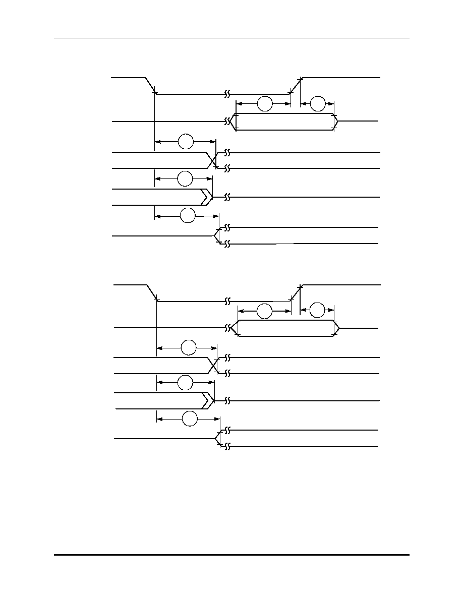
Specifications
JTAG Timing
2-64
DSP56364 Advance Information
MOTOROLA
Figure 2-29 Boundary Scan (JTAG) Timing Diagram
Figure 2-30 Test Access Port Timing Diagram
TCK
(Input)
Data
Inputs
Data
Outputs
Data
Outputs
Data
Outputs
V
IH
V
IL
Input Data Valid
Output Data Valid
Output Data Valid
505
504
506
507
506
AA0497
TCK
(Input)
TDI
(Input)
TDO
(Output)
TDO
(Output)
TDO
(Output)
V
IH
V
IL
Input Data Valid
Output Data Valid
Output Data Valid
TMS
508
509
510
511
510
AA0498
F
r
e
e
s
c
a
l
e
S
e
m
i
c
o
n
d
u
c
t
o
r
,
I
Freescale Semiconductor, Inc.
For More Information On This Product,
Go to: www.freescale.com
n
c
.
.
.

MOTOROLA
DSP56364 Advance Information
3-1
SECTION 3
PACKAGING
3.1
PIN-OUT AND PACKAGE INFORMATION
This section provides information about the available package for this product, including diagrams of the
package pinouts and tables describing how the signals described in
Section 1, Signal/Connection
Descriptions
are allocated for the package. The DSP56364 is available in a 100-pin TQFP package.
Table 3-1
and
Table 3-2
show the pin/name assignments for the packages.
3.1.1
TQFP Package Description
Top view of the 100-pin TQFP package is shown in
Figure 3-1
with its pin-outs. The 100-pin TQFP
package mechanical drawing is shown in
Figure 3-2
.
F
r
e
e
s
c
a
l
e
S
e
m
i
c
o
n
d
u
c
t
o
r
,
I
Freescale Semiconductor, Inc.
For More Information On This Product,
Go to: www.freescale.com
n
c
.
.
.

Packaging
Pin-out and Package Information
3-2
DSP56364 Advance Information
MOTOROLA
Figure 3-1 DSP56364 100-Pin Thin Quad Flat Pack (TQFP), Top View
TM
S
TCK
TDI
TDO
GP
IO
3
GP
IO
2
GP
IO
1
GNDS
V
CCS
GP
IO
0
NC
VC
C
H
Q
GN
D
Q
VC
C
L
Q
NC
NC
D7
D6
D5
D4
GNDD
V
CCD
D3
D2
D1
100
99
98
97
96
95
94
93
92
91
90
89
88
87
86
85
84
83
82
81
80
79
78
77
76
MODD
1
75
D0
MODB
2
74
A17
MODA
3
73
A16
FST
4
72
GNDA
FSR
5
71
VCCA
SCKT
6
70
A15
SCKR
7
69
A14
VCCS
8
68
A13
GNDS
9
DSP56364
100-Pin TQPF
67
A12
HCKT
10
66
VCCLQ
VCCLQ
11
65
GNDQ
GNDQ
12
64
GNDA
HCKR
13
63
VCCA
SDO0
14
62
A11
VCCHQ
15
61
VCCQH
SDO1
16
60
A10
SDO2/SDI3
17
59
A9
SDO3/SDI2
18
58
A8
SDO4/SDI1
19
57
A7
SDO5/SDI0
20
56
GNDA
VCCS
21
55
VCCA
GNDS
22
54
A6
SS/HA2
23
53
A5
MOSI/HA0
24
52
A4
MISO/SDA
25
51
A3
26
27
28
29
30
31
32
33
34
35
36
37
38
39
40
41
42
43
44
45
46
47
48
49
50
S
C
K/
SC
L
HRE
Q
P
I
NIT/
NM
I
RE
S
E
T
NC
V
CCP
PC
A
P
GNDP
EX
TA
L
V
CCHQ
GNDQ
V
CCQL
TA
CA
S
WR
RD
V
CCC
GNDC
AA
1
AA
0
A0
A1
V
CCA
GNDA
A2
F
r
e
e
s
c
a
l
e
S
e
m
i
c
o
n
d
u
c
t
o
r
,
I
Freescale Semiconductor, Inc.
For More Information On This Product,
Go to: www.freescale.com
n
c
.
.
.

Packaging
Pin-out and Package Information
MOTOROLA
DSP56364 Advance Information
3-3
Table 3-1 DSP56364 100-Pin TQFP Signal Identification by Pin Number
Pin
No.
Signal Name
Pin
No.
Signal Name
Pin
No.
Signal Name
Pin
No.
Signal Name
1
MODD/IRQD
26
SCK/SCL
51
A3
76
D1
2
MODB/IRQB
27
HREQ
52
A4
77
D2
3
MODA/IRQA
28
PINIT/NMI
53
A5
78
D3
4
FST
29
RESET
54
A6
79
VCCD
5
FSR
30
No Connect
55
VCCA
80
GNDD
6
SCKT
31
VCCP
56
GNDA
81
D4
7
SCKR
32
PCAP
57
A7
82
D5
8
VCCS
33
GNDP
58
A8
83
D6
9
GNDS
34
EXTAL
59
A9
84
D7
10
HCKT
35
VCCHQ
60
A10
85
No Connect
11
VCCLQ
36
GNDQ
61
VCCHQ
86
No Connect
12
GNDQ
37
VCCLQ
62
A11
87
VCCLQ
13
HCKR
38
TA
63
VCCA
88
GNDQ
14
SDO0
39
CAS
64
GNDA
89
VCCHQ
15
VCCHQ
40
WR
65
GNDQ
90
No Connect
16
SDO1
41
RD
66
VCCLQ
91
GPIO0
17
SDO2/SDI3
42
VCCC
67
A12
92
VCCS
18
SDO3/SDI2
43
GNDC
68
A13
93
GNDS
19
SDO4/SDI1
44
AA1/RAS1
69
A14
94
GPIO1
20
SDO5/SDI0
45
AA0/RAS0
70
A15
95
GPIO2
21
VCCS
46
A0
71
VCCA
96
GPIO3
22
GNDS
47
A1
72
GNDA
97
TDO
23
SS/HA2
48
VCCQ
73
A16
98
TDI
24
MOSI/HA0
49
GNDQ
74
A17
99
TCK
25
MISO/SDA
50
A2
75
D0
100
TMS
Notes:Signal names are based on configured functionality. Most pins supply a single signal. Some pins provide a
signal with dual functionality, such as the MODx/IRQx pins that select an operating mode after RESET is
deasserted, but act as interrupt lines during operation.
F
r
e
e
s
c
a
l
e
S
e
m
i
c
o
n
d
u
c
t
o
r
,
I
Freescale Semiconductor, Inc.
For More Information On This Product,
Go to: www.freescale.com
n
c
.
.
.

Packaging
Pin-out and Package Information
3-4
DSP56364 Advance Information
MOTOROLA
Table 3-2 DSP56364 100-Pin TQFP Signal Identification by Name
Signal Name
Pin
No.
Signal Name
Pin
No.
Signal Name
Pin
No.
Signal Name
Pin
No.
A0
46
D4
81
HCKR
13
SDO4/SDI1
19
A1
47
D5
82
HCKT
10
TA
38
A10
60
D6
83
HREQ
27
TCK
99
A11
62
D7
84
MISO/SDA
25
TDI
98
A12
67
EXTAL
34
MODA/IRQA
3
TD0
97
A13
68
FSR
5
MODB/IRQB
2
TMS
100
A14
69
FST
4
MODD/IRQD
1
VCCA
48
A15
70
GNDA
49
MOSI/HA0
24
VCCA
55
A16
73
GNDA
56
No Connect
30
VCCA
63
A17
74
GNDA
64
No Connect
85
VCCA
71
A2
50
GNDA
72
No Connect
86
VCCC
42
A3
51
GNDC
43
No Connect
90
VCCD
79
A4
52
GNDD
80
PCAP
32
VCCHQ
15
A5
53
GNDP
33
PINIT/NMI
28
VCCHQ
35
A6
54
GNDQ
12
RD
41
VCCHQ
61
A7
57
GNDQ
36
RESET
29
VCCHQ
89
A8
58
GNDQ
65
SCK/SCL
26
VCCLQ
11
A9
59
GNDQ
88
SCKR
7
VCCLQ
37
AA0
45
GNDS
9
SCKT
6
VCCLQ
66
AA1
44
GNDS
22
SDO0
14
VCCLQ
87
CAS
39
GNDS
93
SDO1
16
VCCP
31
D0
75
GPIO0
91
SDO5/SDI0
20
VCCS
8
D1
76
GPIO1
94
SS/HA2
23
VCCS
21
D2
77
GPIO2
95
SDO2/SDI3
17
VCCS
92
D3
78
GPIO3
96
SDO3/SDI2
18
WR
40
F
r
e
e
s
c
a
l
e
S
e
m
i
c
o
n
d
u
c
t
o
r
,
I
Freescale Semiconductor, Inc.
For More Information On This Product,
Go to: www.freescale.com
n
c
.
.
.

Packaging
Pin-out and Package Information
MOTOROLA
DSP56364 Advance Information
3-5
3.1.2
TQFP Package Mechanical Drawing
Figure 3-2 DSP56364 100-pin TQFP Package
F
r
e
e
s
c
a
l
e
S
e
m
i
c
o
n
d
u
c
t
o
r
,
I
Freescale Semiconductor, Inc.
For More Information On This Product,
Go to: www.freescale.com
n
c
.
.
.

Packaging
Ordering Drawings
3-6
DSP56364 Advance Information
MOTOROLA
3.2
ORDERING DRAWINGS
The detailed package drawing is available on the Motorola web page at:
http://mot.sps.com/cgi-bin/cases
Use package 983 for the search.
F
r
e
e
s
c
a
l
e
S
e
m
i
c
o
n
d
u
c
t
o
r
,
I
Freescale Semiconductor, Inc.
For More Information On This Product,
Go to: www.freescale.com
n
c
.
.
.

MOTOROLA
DSP56364 Advance Information
4-1
SECTION 4
DESIGN CONSIDERATIONS
4.1
THERMAL DESIGN CONSIDERATIONS
An estimation of the chip junction temperature, T
J
, in
∞
C can be obtained from the following equation:
Where:
T
A
= ambient temperature
∞
C
R
qJA
= package junction-to-ambient thermal resistance
∞
C/W
P
D
= power dissipation in package W
Historically, thermal resistance has been expressed as the sum of a junction-to-case thermal resistance
and a case-to-ambient thermal resistance.
Where:
R
JA
= package junction-to-ambient thermal resistance ∞C/W
R
JC
= package junction-to-case thermal resistance ∞C/W
R
CA
= package case-to-ambient thermal resistance ∞C/W
R
JC
is device-related and cannot be influenced by the user. The user controls the thermal environment to
change the case-to-ambient thermal resistance, R
CA
. For example, the user can change the air flow
around the device, add a heat sink, change the mounting arrangement on the printed circuit board (PCB),
or otherwise change the thermal dissipation capability of the area surrounding the device on a PCB. This
model is most useful for ceramic packages with heat sinks; some 90% of the heat flow is dissipated
through the case to the heat sink and out to the ambient environment. For ceramic packages, in situations
where the heat flow is split between a path to the case and an alternate path through the PCB, analysis of
the device thermal performance may need the additional modeling capability of a system level thermal
simulation tool.
The thermal performance of plastic packages is more dependent on the temperature of the PCB to which
the package is mounted. Again, if the estimations obtained from R
JA
do not satisfactorily answer whether
the thermal performance is adequate, a system level model may be appropriate.
A complicating factor is the existence of three common ways for determining the junction-to-case thermal
resistance in plastic packages.
∑
To minimize temperature variation across the surface, the thermal resistance is measured from the
junction to the outside surface of the package (case) closest to the chip mounting area when that
surface has a proper heat sink.
∑
To define a value approximately equal to a junction-to-board thermal resistance, the thermal
resistance is measured from the junction to where the leads are attached to the case.
∑
If the temperature of the package case (T
T
) is determined by a thermocouple, the thermal
resistance is computed using the value obtained by the equation
(T
J
≠ T
T
)/P
D
.
T
J
T
A
P
D
R
JA
◊
(
)
+
=
R
JA
R
JC
R
CA
+
=
F
r
e
e
s
c
a
l
e
S
e
m
i
c
o
n
d
u
c
t
o
r
,
I
Freescale Semiconductor, Inc.
For More Information On This Product,
Go to: www.freescale.com
n
c
.
.
.

Design Considerations
Electrical Design Considerations
4-2
DSP56364 Advance Information
MOTOROLA
As noted above, the junction-to-case thermal resistances quoted in this data sheet are determined using
the first definition. From a practical standpoint, that value is also suitable for determining the junction
temperature from a case thermocouple reading in forced convection environments. In natural convection,
using the junction-to-case thermal resistance to estimate junction temperature from a thermocouple
reading on the case of the package will estimate a junction temperature slightly hotter than actual
temperature. Hence, the new thermal metric, thermal characterization parameter or
JT
, has been defined
to be (T
J
≠ T
T
)/P
D
. This value gives a better estimate of the junction temperature in natural convection
when using the surface temperature of the package. Remember that surface temperature readings of
packages are subject to significant errors caused by inadequate attachment of the sensor to the surface
and to errors caused by heat loss to the sensor. The recommended technique is to attach a 40-gauge
thermocouple wire and bead to the top center of the package with thermally conductive epoxy.
4.2
ELECTRICAL DESIGN CONSIDERATIONS
Use the following list of recommendations to assure correct DSP operation:
∑
Provide a low-impedance path from the board power supply to each V
CC
pin on the DSP and from
the board ground to each GND pin.
∑
Use at least six 0.01≠0.1
µ
F bypass capacitors positioned as close as possible to the four sides of
the package to connect the V
CC
power source to GND.
∑
Ensure that capacitor leads and associated printed circuit traces that connect to the chip V
CC
and
GND pins are less than 1.2 cm (0.5 inch) per capacitor lead.
∑
Use at least a four-layer PCB with two inner layers for V
CC
and GND.
∑
Because the DSP output signals have fast rise and fall times, PCB trace lengths should be minimal.
This recommendation particularly applies to the address and data buses as well as the IRQA, IRQB,
IRQD, and TA pins. Maximum PCB trace lengths on the order of 15 cm (6 inches) are
recommended.
∑
Consider all device loads as well as parasitic capacitance due to PCB traces when calculating
capacitance. This is especially critical in systems with higher capacitive loads that could create
higher transient currents in the V
CC
and GND circuits.
CAUTION
This device contains circuitry protecting
against damage due to high static voltage or
electrical fields. However, normal precautions
should be taken to avoid exceeding maximum
voltage ratings. Reliability of operation is
enhanced if unused inputs are tied to an
appropriate logic voltage level (e.g., either
GND or V
CC
). The suggested value for a
pullup or pulldown resistor is 10 k ohm.
F
r
e
e
s
c
a
l
e
S
e
m
i
c
o
n
d
u
c
t
o
r
,
I
Freescale Semiconductor, Inc.
For More Information On This Product,
Go to: www.freescale.com
n
c
.
.
.

Design Considerations
Power Consumption Considerations
MOTOROLA
DSP56364 Advance Information
4-3
∑
All inputs must be terminated (i.e., not allowed to float) using CMOS levels, except for the three pins
with internal pull-up resistors (TMS, TDI, TCK).
∑
Take special care to minimize noise levels on the V
CCP
and GND
P
pins.
∑
If multiple DSP56364 devices are on the same board, check for cross-talk or excessive spikes on
the supplies due to synchronous operation of the devices.
∑
RESET must be asserted when the chip is powered up. A stable EXTAL signal must be supplied
before deassertion of RESET.
∑
At power-up, ensure that the voltage difference between the 5 V tolerant pins and the chip V
CC
never exceeds 3.95 V.
4.3
POWER CONSUMPTION CONSIDERATIONS
Power dissipation is a key issue in portable DSP applications. Some of the factors which affect current
consumption are described in this section. Most of the current consumed by CMOS devices is alternating
current (ac), which is charging and discharging the capacitances of the pins and internal nodes.
Current consumption is described by the following formula:
where
C = node/pin capacitance
V = voltage swing
f = frequency of node/pin toggle
The maximum internal current (I
CCI
max) value reflects the typical possible switching of the internal buses
on best-case operation conditions, which is not necessarily a real application case. The typical internal
current (I
CCItyp
) value reflects the average switching of the internal buses on typical operating conditions.
For applications that require very low current consumption, do the following:
∑
Set the EBD bit when not accessing external memory.
∑
Minimize external memory accesses and use internal memory accesses.
∑
Minimize the number of pins that are switching.
∑
Minimize the capacitive load on the pins.
∑
Connect the unused inputs to pull-up or pull-down resistors.
∑
Disable unused peripherals.
Example 1 Current Consumption
For a Port A address pin loaded with 50 pF capacitance, operating at 3.3 V, and with a 100 MHz
clock, toggling at its maximum possible rate (50 MHz), the current consumption is
I
C
V
f
◊
◊
=
I
50
10
12
≠
◊
3.3
◊
50
◊
10
6
◊
8.25mA
=
=
F
r
e
e
s
c
a
l
e
S
e
m
i
c
o
n
d
u
c
t
o
r
,
I
Freescale Semiconductor, Inc.
For More Information On This Product,
Go to: www.freescale.com
n
c
.
.
.

Design Considerations
PLL Performance Issues
4-4
DSP56364 Advance Information
MOTOROLA
One way to evaluate power consumption is to use a current per MIPS measurement methodology to
minimize specific board effects (i.e., to compensate for measured board current not caused by the DSP). A
benchmark power consumption test algorithm is listed in
Appendix A
. Use the test algorithm, specific test
current measurements, and the following equation to derive the current per MIPS value.
where :
I
typF2
= current at F2
I
typF1
= current at F1
F2 = high frequency (any specified operating frequency)
F1 = low frequency (any specified operating frequency lower than F2)
Note:
F1 should be significantly less than F2. For example, F2 could be 66 MHz and F1
could be 33 MHz. The degree of difference between F1 and F2 determines the
amount of precision with which the current rating can be determined for an
application.
4.4
PLL PERFORMANCE ISSUES
The following explanations should be considered as general observations on expected PLL behavior.
There is no testing that verifies these exact numbers. These observations were measured on a limited
number of parts and were not verified over the entire temperature and voltage ranges.
4.4.1
Input (EXTAL) Jitter Requirements
The allowed jitter on the frequency of EXTAL is 0.5%. If the rate of change of the frequency of EXTAL is
slow (i.e., it does not jump between the minimum and maximum values in one cycle) or the frequency of
the jitter is fast (i.e., it does not stay at an extreme value for a long time), then the allowed jitter can be 2%.
The phase and frequency jitter performance results are only valid if the input jitter is less than the
prescribed values.
I MIPS
/
I MHz
/
I
typF2
I
typF1
≠
(
)
F2
F1
≠
(
)
/
=
=
F
r
e
e
s
c
a
l
e
S
e
m
i
c
o
n
d
u
c
t
o
r
,
I
Freescale Semiconductor, Inc.
For More Information On This Product,
Go to: www.freescale.com
n
c
.
.
.

MOTOROLA
DSP56364 Advance Information
5-1
SECTION 5
ORDERING INFORMATION
Consult a Motorola Semiconductor sales office or authorized distributor to determine product availability
and to place an order.
Table 5-1 Ordering Information
Part
Supply
Voltage
Package Type
Pin
Count
Frequency
(MHz)
Order Number
DSP56364
3.3 V
Thin quad flat pack (TQFP)
100
100
XCB56364FU100
Quad flat pack (QFP)
112
100
XCB56364PV100
Notes:
1.
The DSP56364 can include factory-programmed ROM. The listed `B' ROM code is a generic unused
ROM available to any customer. Variations will be supported for Dolby digital (AC-3), DTS, MPEG2,
and other features. These products are only available to authorized licensees of those technologies.
Please consult the web site at www.dspaudio.motorola.com for current availability.
2.
Future products in the DSP56364 family may include other ROM-based options. For additional
information on future part development, or to request customer-specific ROM-based support, call
your local Motorola Semiconductor sales office or authorized distributor.
F
r
e
e
s
c
a
l
e
S
e
m
i
c
o
n
d
u
c
t
o
r
,
I
Freescale Semiconductor, Inc.
For More Information On This Product,
Go to: www.freescale.com
n
c
.
.
.

THIS PAGE INTENTIONALLY LEFT BLANK
F
r
e
e
s
c
a
l
e
S
e
m
i
c
o
n
d
u
c
t
o
r
,
I
Freescale Semiconductor, Inc.
For More Information On This Product,
Go to: www.freescale.com
n
c
.
.
.

MOTOROLA
DSP56364 Advance Information
A-1
APPENDIX A
IBIS MODEL
IBIS Model
[IBIS Ver] 3.2
[File name] 56364_e.ibs
[File Rev] e
[Date] Feb 13, 2002
[Component] 56364
[Manufacturer] MOTOROLA SEMI CONDUCTOR Ltd.
[Package]
| variable typ min max
R_pkg 45.0m 22.0m 75.0m
L_pkg 2.5nH 1.1nH 4.3nH
C_pkg 1.3pF 1.2pF 1.4pF
[Pin] signal_name model_name R_pin L_pin
C_pin
1 irqd_ ipad5v_io
2 irqb_ ipad5v_io
3 irqa_ ipad5v_io
4 fst ipad5v_io
5 fsr ipad5v_io
6 sckt ipad5v_io
7 sckr ipad5v_io
8 vccs power
9 gnds gnd
10 hckt ipad5v_io
11 vcclq power
12 gndq gnd
13 hckr ipad5v_io
14 sdo0 ipad5v_io
15 vcchq power
16 sdo1 ipad5v_io
17 sdo2/sdi3 ipad5v_io
18 sdo3/sdi2 ipad5v_io
19 sdo4/sdi1 ipad5v_io
20 sdo5/sdi0 ipad5v_io
21 vccs power
22 gnds gnd
23 ss_/ha2 ipad5v_io
24 mosi/ha0 ipad5v_io
25 miso/sda ipad5i_io
26 sck/scl ipad5i_io
27 hreq_ ipad5i_io
28 pinit/nmi_ ipad5v_io
29 reset_ ipad5v_io
31 vccp power
32 pcap power
33 gndp gnd
34 extal ipadex_i
35 vcchq power
F
r
e
e
s
c
a
l
e
S
e
m
i
c
o
n
d
u
c
t
o
r
,
I
Freescale Semiconductor, Inc.
For More Information On This Product,
Go to: www.freescale.com
n
c
.
.
.

IBIS Model
A-2
DSP56364 Advance Information
MOTOROLA
36 gndq gnd
37 vcclq power
38 ta_ ipadn_io
39 cas_ ipadm_3st
40 wr_ ipadn_io
41 rd_ ipadn_io
42 vccc power
43 gndc gnd
44 aa1/ras1_ ipado_3st
45 aa0/ras0_ ipado_3st
46 a0 ipada_3st
47 a1 ipada_3st
48 vccq power
49 gndq gnd
50 a2 ipada_3st
51 a3 ipada_3st
52 a4 ipada_3st
53 a5 ipada_3st
54 a6 ipada_3st
55 vcca power
56 gnda gnd
57 a7 ipada_3st
58 a8 ipada_3st
59 a9 ipada_3st
60 a10 ipada_3st
61 vcchq power
62 a11 ipada_3st
63 vcca power
64 gnda gnd
65 gndq gnd
66 vcclq power
67 a12 power
68 a13 ipada_3st
69 a14 ipada_3st
70 a15 ipada_3st
71 vcca power
72 gnda gnd
73 a16 ipada_3st
74 a17 ipada_3st
75 d0 ipadd_io
76 d1 ipadd_io
77 d2 ipadd_io
78 d3 ipadd_io
79 vccd power
80 gndd gnd
81 d4 ipadd_io
82 d5 ipadd_io
83 d6 ipadd_io
84 d7 ipadd_io
87 vcclq power
88 gndq gnd
89 vcchq power
91 gpio0 ipad5v_io
F
r
e
e
s
c
a
l
e
S
e
m
i
c
o
n
d
u
c
t
o
r
,
I
Freescale Semiconductor, Inc.
For More Information On This Product,
Go to: www.freescale.com
n
c
.
.
.

IBIS Model
MOTOROLA
DSP56364 Advance Information
A-3
92 vccs power
93 gnds gnd
94 gpio1 ipad5v_io
95 gpio2 ipad5v_io
96 gpio3 ipad5v_io
97 tdo ipad5f_io
98 tdi ipad5f_io
99 tck ipad5f_io
100 tms ipad5f_io
[Model] ipad5f_io | ""
Model_type I/O
Vinl = 0.8
Vinh = 2
| variable typ min max
C_comp 1.96p 1.87p 2.06p
| variable typ min max
[Temperature Range] 40.0 0.0 120.0
| variable typ min max
[Voltage Range] 3.30V 3.00V 3.60V
|
[Pulldown]
| pulldown in the table = pulldown subtract gnd_clamp
|Voltage I(typ) I(min) I(max)
|
-3.30V -142.303u -76.239u -215.182u
-3.20V -149.700u -80.226u -226.432u
-3.10V -157.861u -84.616u -238.866u
-3.00V -166.908u -89.472u -252.678u
-2.90V -176.992u -94.869u -268.107u
-2.80V -188.295u -100.900u -285.446u
-2.70V -201.049u -107.679u -305.068u
-2.60V -215.545u -115.349u -327.446u
-2.50V -232.155u -124.094u -353.191u
-2.40V -251.367u -134.145u -383.107u
-2.30V -273.825u -145.808u -418.273u
-2.20V -300.403u -159.488u -460.167u
-2.10V -332.314u -175.737u -510.874u
-2.00V -371.286u -195.318u -573.418u
-1.90V -419.868u -219.325u -652.360u
-1.80V -481.968u -249.369u -754.892u
-1.70V -563.882u -287.925u -893.013u
-1.60V -676.382u -338.973u -1.088m
-1.50V -839.410u -409.300u -1.383m
-1.40V -1.094m -511.367u -1.873m
-1.30V -1.537m -670.350u -2.819m
-1.20V -2.451m -943.845u -5.162m
-1.10V -4.857m -1.486m -12.214m
-1.00V -10.606m -2.746m -20.764m
-0.90V -14.267m -5.259m -21.749m
-0.80V -13.851m -7.108m -20.142m
-0.70V -12.481m -7.168m -18.211m
-0.60V -10.883m -6.348m -15.981m
F
r
e
e
s
c
a
l
e
S
e
m
i
c
o
n
d
u
c
t
o
r
,
I
Freescale Semiconductor, Inc.
For More Information On This Product,
Go to: www.freescale.com
n
c
.
.
.

IBIS Model
A-4
DSP56364 Advance Information
MOTOROLA
-0.50V -9.156m -5.339m -13.503m
-0.40V -7.378m -4.288m -10.922m
-0.30V -5.572m -3.224m -8.282m
-0.20V -3.741m -2.154m -5.584m
-0.10V -1.885m -1.080m -2.825m
0.00V 1.898p 1.419p 1.871p
0.10V 1.857m 1.057m 2.800m
0.20V 3.630m 2.064m 5.482m
0.30V 5.323m 3.023m 8.052m
0.40V 6.936m 3.935m 10.508m
0.50V 8.467m 4.798m 12.849m
0.60V 9.915m 5.611m 15.073m
0.70V 11.275m 6.371m 17.176m
0.80V 12.546m 7.078m 19.155m
0.90V 13.723m 7.726m 21.011m
1.00V 36.925m 20.745m 56.704m
1.10V 39.391m 22.074m 60.708m
1.20V 41.612m 23.244m 64.383m
1.30V 43.585m 24.247m 67.726m
1.40V 45.305m 25.079m 70.735m
1.50V 46.773m 25.741m 73.414m
1.60V 47.997m 26.251m 75.766m
1.70V 48.985m 26.633m 77.783m
1.80V 49.733m 26.905m 79.441m
1.90V 50.257m 27.092m 80.724m
2.00V 50.612m 27.223m 81.651m
2.10V 50.858m 27.321m 82.294m
2.20V 51.040m 27.399m 82.744m
2.30V 51.182m 27.465m 83.074m
2.40V 51.302m 27.522m 83.332m
2.50V 51.405m 27.572m 83.543m
2.60V 51.497m 27.618m 83.724m
2.70V 51.581m 27.657m 83.884m
2.80V 51.658m 27.674m 84.030m
2.90V 51.727m 27.587m 84.165m
3.00V 51.757m 27.577m 84.290m
3.10V 51.229m 28.700m 84.409m
3.20V 49.190m 30.042m 84.515m
3.30V 49.441m 31.171m 84.491m
3.40V 51.034m 32.199m 81.077m
3.50V 54.363m 33.153m 79.736m
3.60V 57.165m 34.039m 80.276m
3.70V 58.834m 34.872m 82.430m
3.80V 60.328m 35.686m 85.482m
3.90V 61.725m 36.495m 91.743m
4.00V 63.035m 37.291m 94.219m
4.10V 64.319m 38.051m 96.276m
4.20V 65.598m 38.755m 98.249m
4.30V 66.836m 39.394m 100.059m
4.40V 67.999m 39.962m 101.849m
4.50V 69.069m 40.453m 103.628m
4.60V 70.046m 40.840m 105.345m
4.70V 70.938m 41.065m 106.956m
F
r
e
e
s
c
a
l
e
S
e
m
i
c
o
n
d
u
c
t
o
r
,
I
Freescale Semiconductor, Inc.
For More Information On This Product,
Go to: www.freescale.com
n
c
.
.
.

IBIS Model
MOTOROLA
DSP56364 Advance Information
A-5
4.80V 71.751m 40.952m 108.448m
4.90V 72.476m 40.067m 109.826m
5.00V 73.089m 39.395m 111.106m
5.10V 73.531m 39.313m 112.297m
5.20V 73.651m 39.358m 113.400m
5.30V 72.901m 39.410m 114.401m
5.40V 71.005m 39.460m 115.267m
5.50V 70.389m 39.508m 115.917m
5.60V 70.321m 39.552m 116.139m
5.70V 70.361m 39.595m 114.582m
5.80V 70.422m 39.634m 111.344m
5.90V 70.489m 39.672m 110.612m
6.00V 70.557m 39.708m 110.449m
6.10V 70.624m 39.743m 110.455m
6.20V 70.690m 39.777m 110.515m
6.30V 70.753m 39.812m 110.595m
6.40V 70.817m 39.848m 110.686m
6.50V 70.881m 39.886m 110.783m
6.60V 70.949m 39.929m 110.885m
|
[Pullup]
| pullup in the table = pullup subtract power_clamp
|Voltage I(typ) I(min) I(max)
|
-3.30V 75.797u 7.914u 161.477u
-3.20V 90.464u 17.699u 181.779u
-3.10V 105.160u 27.445u 202.314u
-3.00V 119.836u 37.119u 223.007u
-2.90V 134.451u 46.694u 243.785u
-2.80V 148.966u 56.144u 264.581u
-2.70V 163.342u 65.447u 285.332u
-2.60V 177.543u 74.582u 305.982u
-2.50V 191.536u 83.527u 326.474u
-2.40V 205.285u 92.262u 346.757u
-2.30V 218.754u 100.766u 366.776u
-2.20V 231.907u 109.016u 386.478u
-2.10V 244.706u 116.988u 405.807u
-2.00V 257.106u 124.659u 424.699u
-1.90V 269.061u 131.998u 443.089u
-1.80V 280.519u 138.978u 460.899u
-1.70V 291.423u 145.565u 478.046u
-1.60V 301.710u 151.723u 494.457u
-1.50V 311.348u 157.417u 521.406u
-1.40V 729.899u 162.626u 1.612m
-1.30V 10.510m 445.517u 14.832m
-1.20V 9.629m 6.444m 13.576m
-1.10V 8.670m 5.833m 12.231m
-1.00V 7.693m 5.190m 10.854m
-0.90V 6.732m 4.551m 9.483m
-0.80V 5.825m 3.942m 8.169m
-0.70V 5.004m 3.382m 6.971m
-0.60V 4.261m 2.869m 5.921m
-0.50V 3.549m 2.381m 4.953m
F
r
e
e
s
c
a
l
e
S
e
m
i
c
o
n
d
u
c
t
o
r
,
I
Freescale Semiconductor, Inc.
For More Information On This Product,
Go to: www.freescale.com
n
c
.
.
.

IBIS Model
A-6
DSP56364 Advance Information
MOTOROLA
-0.40V 2.841m 1.902m 3.978m
-0.30V 2.135m 1.426m 2.987m
-0.20V 1.437m 951.489u 2.003m
-0.10V 722.340u 478.341u 1.005m
-0.00V 22.329p 3.311p 24.081p
0.10V -708.556u -465.927u -990.647u
0.20V -1.377m -903.637u -1.943m
0.30V -2.007m -1.319m -2.832m
0.40V -2.614m -1.710m -3.702m
0.50V -3.192m -2.079m -4.537m
0.60V -3.738m -2.423m -5.336m
0.70V -4.253m -2.742m -6.096m
0.80V -4.736m -3.037m -6.817m
0.90V -5.185m -3.305m -7.499m
1.00V -5.600m -3.547m -8.139m
1.10V -5.980m -3.762m -8.737m
1.20V -6.324m -3.948m -9.292m
1.30V -6.631m -17.709m -9.802m
1.40V -29.730m -18.279m -10.265m
1.50V -30.749m -18.747m -45.983m
1.60V -31.630m -19.131m -47.620m
1.70V -32.393m -19.454m -49.086m
1.80V -33.055m -19.730m -50.392m
1.90V -33.632m -19.973m -51.551m
2.00V -34.135m -20.188m -52.571m
2.10V -34.575m -20.381m -53.463m
2.20V -34.960m -20.556m -54.240m
2.30V -35.302m -20.715m -54.917m
2.40V -35.608m -20.861m -55.510m
2.50V -35.884m -20.997m -56.035m
2.60V -36.137m -21.123m -56.505m
2.70V -36.370m -21.241m -56.932m
2.80V -36.586m -21.352m -57.322m
2.90V -36.788m -21.457m -57.683m
3.00V -36.978m -21.556m -58.019m
3.10V -37.157m -21.650m -58.334m
3.20V -37.327m -21.741m -58.631m
3.30V -37.489m -21.827m -58.913m
3.40V -37.643m -21.909m -59.181m
3.50V -37.791m -21.989m -59.436m
3.60V -37.933m -22.067m -59.681m
3.70V -38.070m -22.143m -59.916m
3.80V -38.202m -22.216m -60.142m
3.90V -38.332m -22.284m -60.361m
4.00V -38.460m -22.352m -60.573m
4.10V -38.590m -22.420m -60.780m
4.20V -38.714m -22.490m -60.986m
4.30V -38.828m -22.561m -61.194m
4.40V -38.949m -22.635m -61.406m
4.50V -39.076m -22.713m -61.623m
4.60V -39.211m -22.798m -61.819m
4.70V -39.357m -22.892m -62.024m
4.80V -39.516m -22.997m -62.254m
F
r
e
e
s
c
a
l
e
S
e
m
i
c
o
n
d
u
c
t
o
r
,
I
Freescale Semiconductor, Inc.
For More Information On This Product,
Go to: www.freescale.com
n
c
.
.
.

IBIS Model
MOTOROLA
DSP56364 Advance Information
A-7
4.90V -39.693m -23.116m -62.506m
5.00V -39.893m -23.253m -62.785m
5.10V -40.121m -23.411m -63.098m
5.20V -40.384m -23.595m -63.453m
5.30V -40.689m -23.801m -63.860m
5.40V -41.043m -24.032m -64.330m
5.50V -41.444m -24.288m -64.874m
5.60V -41.886m -24.570m -65.505m
5.70V -42.370m -24.880m -66.214m
5.80V -42.899m -25.217m -66.983m
5.90V -43.473m -25.585m -67.815m
6.00V -44.095m -25.983m -68.711m
6.10V -44.769m -26.415m -69.678m
6.20V -45.498m -26.884m -70.721m
6.30V -46.287m -27.390m -71.848m
6.40V -47.140m -27.929m -73.065m
6.50V -48.049m -28.487m -74.374m
6.60V -48.990m -29.080m -75.748m
|
[GND_clamp]
|
|Voltage I(typ) I(min) I(max)
|
-3.30V -1.875 -1.074 -2.155
-3.20V -1.793 -1.029 -2.059
-3.10V -1.711 -983.765m -1.963
-2.90V -1.548 -893.931m -1.771
-2.80V -1.466 -849.071m -1.675
-2.70V -1.385 -804.256m -1.579
-2.60V -1.303 -759.489m -1.483
-2.50V -1.221 -714.777m -1.388
-2.40V -1.140 -670.127m -1.292
-2.30V -1.059 -625.548m -1.197
-2.20V -977.735m -581.048m -1.102
-2.10V -896.773m -536.642m -1.007
-1.90V -735.446m -448.177m -817.634m
-1.80V -655.171m -404.164m -723.409m
-1.70V -575.242m -360.342m -629.587m
-1.60V -495.760m -316.758m -536.295m
-1.50V -416.878m -273.482m -443.730m
-1.40V -338.839m -230.618m -352.222m
-1.30V -262.067m -188.327m -262.384m
-1.20V -187.395m -146.891m -175.533m
-1.10V -116.756m -106.839m -95.231m
-0.90V -16.024m -37.029m -6.612m
-0.80V -2.254m -14.319m -2.370m
-0.70V -476.015u -2.883m -845.181u
-0.60V -85.877u -295.354u -147.930u
-0.50V -8.033u -33.637u -9.999u
-0.40V -432.304n -3.576u -310.975n
-0.30V -20.874n -340.944n -8.593n
-0.20V -964.564p -30.895n -258.649p
-0.10V -72.583p -2.560n -43.910p
F
r
e
e
s
c
a
l
e
S
e
m
i
c
o
n
d
u
c
t
o
r
,
I
Freescale Semiconductor, Inc.
For More Information On This Product,
Go to: www.freescale.com
n
c
.
.
.

IBIS Model
A-8
DSP56364 Advance Information
MOTOROLA
0.00V -33.685p -210.508p -34.610p
0.10V -27.665p -30.628p -29.748p
0.20V -22.754p 13.546p -25.110p
0.30V -18.303p 48.356p -20.906p
0.40V -14.129p 81.869p -16.971p
0.50V -9.979p 114.849p -13.050p
0.60V -5.833p 147.499p -9.130p
0.70V -1.689p 179.924p -5.210p
0.80V 2.454p 212.188p -1.291p
0.90V 6.596p 244.335p 2.628p
1.10V 14.877p 308.388p 10.466p
1.20V 19.017p 340.335p 14.384p
1.30V 23.157p 372.250p 18.302p
1.40V 27.297p 404.143p 22.221p
1.50V 31.436p 436.027p 26.139p
1.60V 35.576p 467.910p 30.057p
1.70V 39.715p 499.805p 33.974p
1.80V 43.855p 531.722p 37.892p
1.90V 47.995p 563.675p 41.810p
2.10V 56.277p 627.761p 49.646p
2.20V 60.418p 659.933p 53.564p
2.30V 64.561p 692.106p 57.482p
2.40V 68.706p 723.142p 61.400p
2.50V 72.847p 751.973p 65.319p
2.60V 76.869p 780.264p 69.237p
2.70V 80.074p 808.442p 73.156p
2.80V 82.499p 835.513p 77.065p
2.90V 84.837p 860.391p 80.794p
3.10V 89.018p 1.265n 86.195p
3.20V 89.573p 1.305n 88.344p
3.30V 103.108p 1.593n 90.478p
|
[POWER_clamp]
|
|Voltage I(typ) I(min) I(max)
|
3.30V -33.685p -340.944n -20.906p
3.40V -72.583p -3.576u -25.110p
3.50V -964.564p -33.637u -29.748p
3.60V -20.874n -295.354u -34.610p
3.70V -432.304n -2.883m -43.910p
3.80V -8.033u -14.319m -258.649p
3.90V -85.877u -37.029m -8.593n
4.10V -2.254m -106.839m -9.999u
4.20V -16.024m -146.891m -147.930u
4.30V -55.636m -188.327m -845.181u
4.40V -116.756m -230.618m -2.370m
4.50V -187.395m -273.482m -6.612m
4.60V -262.067m -316.758m -33.199m
4.70V -338.839m -360.342m -95.231m
4.80V -416.878m -404.164m -175.533m
4.90V -495.760m -448.177m -262.384m
5.10V -655.171m -536.642m -443.730m
F
r
e
e
s
c
a
l
e
S
e
m
i
c
o
n
d
u
c
t
o
r
,
I
Freescale Semiconductor, Inc.
For More Information On This Product,
Go to: www.freescale.com
n
c
.
.
.

IBIS Model
MOTOROLA
DSP56364 Advance Information
A-9
5.20V -735.446m -581.048m -536.295m
5.30V -815.997m -625.548m -629.587m
5.40V -896.773m -670.127m -723.409m
5.50V -977.735m -714.777m -817.634m
5.60V -1.059 -759.489m -912.174m
5.70V -1.140 -804.256m -1.007
5.80V -1.221 -849.071m -1.102
5.90V -1.303 -893.931m -1.197
6.10V -1.466 -983.765m -1.388
6.20V -1.548 -1.029 -1.483
6.30V -1.630 -1.074 -1.579
6.40V -1.711 -1.119 -1.675
6.50V -1.793 -1.164 -1.771
6.60V -1.875 -1.209 -1.867
|
[Ramp]
|Voltage I(typ) I(min) I(max)
|
dV/dt_f 2.04/136.004p 1.86/237.542p 2.23/85.504p
|
dV/dt_r 2.05/194.744p 1.86/343.805p 2.23/118.850p
R_load=10000ohms
| R_load was connected to ground for Ramp_up test and power for Ramp_dn
test
|
|End model
[Model] ipad5i_io | ""
Model_type I/O
Vinl = 0.8
Vinh = 2
| variable typ min max
C_comp 4.44p 3.89p 4.56p
| variable typ min max
[Temperature Range] 40.0 0.0 120.0
| variable typ min max
[Voltage Range] 3.30V 3.00V 3.60V
|
[Pulldown]
| pulldown in the table = pulldown subtract gnd_clamp
|Voltage I(typ) I(min) I(max)
|
-3.30V -142.303u -76.239u -215.182u
-3.20V -149.700u -80.226u -226.432u
-3.10V -157.861u -84.616u -238.866u
-3.00V -166.908u -89.472u -252.678u
-2.90V -176.992u -94.869u -268.107u
-2.80V -188.295u -100.900u -285.446u
-2.70V -201.049u -107.679u -305.068u
-2.60V -215.545u -115.349u -327.446u
-2.50V -232.155u -124.094u -353.191u
-2.40V -251.367u -134.145u -383.107u
-2.30V -273.825u -145.808u -418.273u
-2.20V -300.403u -159.488u -460.167u
F
r
e
e
s
c
a
l
e
S
e
m
i
c
o
n
d
u
c
t
o
r
,
I
Freescale Semiconductor, Inc.
For More Information On This Product,
Go to: www.freescale.com
n
c
.
.
.

IBIS Model
A-10
DSP56364 Advance Information
MOTOROLA
-2.10V -332.314u -175.737u -510.874u
-2.00V -371.286u -195.318u -573.418u
-1.90V -419.868u -219.325u -652.360u
-1.80V -481.968u -249.369u -754.892u
-1.70V -563.882u -287.925u -893.013u
-1.60V -676.382u -338.973u -1.088m
-1.50V -839.410u -409.300u -1.383m
-1.40V -1.094m -511.367u -1.873m
-1.30V -1.537m -670.350u -2.819m
-1.20V -2.451m -943.845u -5.162m
-1.10V -4.857m -1.486m -12.214m
-1.00V -10.606m -2.746m -20.764m
-0.90V -14.267m -5.259m -21.749m
-0.80V -13.851m -7.108m -20.142m
-0.70V -12.481m -7.168m -18.211m
-0.60V -10.883m -6.348m -15.981m
-0.50V -9.156m -5.339m -13.503m
-0.40V -7.378m -4.288m -10.922m
-0.30V -5.572m -3.224m -8.282m
-0.20V -3.741m -2.154m -5.584m
-0.10V -1.885m -1.080m -2.825m
0.00V 1.898p 1.419p 1.871p
0.10V 1.857m 1.057m 2.800m
0.20V 3.630m 2.064m 5.482m
0.30V 5.323m 3.023m 8.052m
0.40V 6.936m 3.935m 10.508m
0.50V 8.467m 4.798m 12.849m
0.60V 9.915m 5.611m 15.073m
0.70V 11.275m 6.371m 17.176m
0.80V 12.546m 7.078m 19.155m
0.90V 13.723m 7.726m 21.011m
1.00V 36.925m 20.745m 56.704m
1.10V 39.391m 22.074m 60.708m
1.20V 41.612m 23.244m 64.383m
1.30V 43.585m 24.247m 67.726m
1.40V 45.305m 25.079m 70.735m
1.50V 46.773m 25.741m 73.414m
1.60V 47.997m 26.251m 75.766m
1.70V 48.985m 26.633m 77.783m
1.80V 49.733m 26.905m 79.441m
1.90V 50.257m 27.092m 80.724m
2.00V 50.612m 27.223m 81.651m
2.10V 50.858m 27.321m 82.294m
2.20V 51.040m 27.399m 82.744m
2.30V 51.182m 27.465m 83.074m
2.40V 51.302m 27.522m 83.332m
2.50V 51.405m 27.572m 83.543m
2.60V 51.497m 27.618m 83.724m
2.70V 51.581m 27.658m 83.884m
2.80V 51.658m 27.683m 84.030m
2.90V 51.729m 27.643m 84.165m
3.00V 51.781m 27.704m 84.290m
3.10V 51.640m 28.793m 84.409m
F
r
e
e
s
c
a
l
e
S
e
m
i
c
o
n
d
u
c
t
o
r
,
I
Freescale Semiconductor, Inc.
For More Information On This Product,
Go to: www.freescale.com
n
c
.
.
.

IBIS Model
MOTOROLA
DSP56364 Advance Information
A-11
3.20V 50.282m 30.065m 84.519m
3.30V 50.273m 31.174m 84.574m
3.40V 51.871m 32.200m 83.365m
3.50V 55.121m 33.153m 80.948m
3.60V 57.228m 34.039m 81.423m
3.70V 58.838m 34.872m 83.424m
3.80V 60.328m 35.687m 87.158m
3.90V 61.725m 36.498m 91.951m
4.00V 63.035m 37.296m 94.228m
4.10V 64.321m 38.059m 96.276m
4.20V 65.602m 38.767m 98.249m
4.30V 66.844m 39.409m 100.060m
4.40V 68.012m 39.982m 101.853m
4.50V 69.088m 40.478m 103.638m
4.60V 70.072m 40.871m 105.361m
4.70V 70.973m 41.102m 106.982m
4.80V 71.794m 40.996m 108.484m
4.90V 72.529m 40.118m 109.875m
5.00V 73.152m 39.453m 111.168m
5.10V 73.605m 39.379m 112.374m
5.20V 73.737m 39.432m 113.492m
5.30V 72.999m 39.492m 114.510m
5.40V 71.115m 39.551m 115.392m
5.50V 70.512m 39.608m 116.061m
5.60V 70.457m 39.661m 116.301m
5.70V 70.511m 39.713m 114.763m
5.80V 70.586m 39.762m 111.545m
5.90V 70.667m 39.809m 110.833m
6.00V 70.749m 39.855m 110.689m
6.10V 70.831m 39.899m 110.716m
6.20V 70.911m 39.944m 110.796m
6.30V 70.989m 39.988m 110.897m
6.40V 71.068m 40.034m 111.009m
6.50V 71.148m 40.083m 111.127m
6.60V 71.230m 40.136m 111.250m
|
[Pullup]
| pullup in the table = pullup subtract power_clamp
|Voltage I(typ) I(min) I(max)
|
-3.30V 357.190u 184.381u 591.381u
-3.20V 356.622u 184.121u 590.188u
-3.10V 356.193u 183.920u 589.287u
-3.00V 355.875u 183.765u 588.617u
-2.90V 355.641u 183.645u 588.129u
-2.80V 355.468u 183.550u 587.779u
-2.70V 355.340u 183.472u 587.528u
-2.60V 355.242u 183.405u 587.349u
-2.50V 355.163u 183.345u 587.218u
-2.40V 355.097u 183.288u 587.118u
-2.30V 355.036u 183.233u 587.036u
-2.20V 354.978u 183.177u 586.964u
-2.10V 354.920u 183.119u 586.896u
F
r
e
e
s
c
a
l
e
S
e
m
i
c
o
n
d
u
c
t
o
r
,
I
Freescale Semiconductor, Inc.
For More Information On This Product,
Go to: www.freescale.com
n
c
.
.
.

IBIS Model
A-12
DSP56364 Advance Information
MOTOROLA
-2.00V 354.860u 183.060u 586.829u
-1.90V 354.799u 182.997u 586.762u
-1.80V 354.734u 182.931u 586.692u
-1.70V 354.666u 182.862u 586.621u
-1.60V 354.595u 182.788u 586.574u
-1.50V 354.559u 182.711u 597.934u
-1.40V 764.198u 182.650u 1.674m
-1.30V 10.536m 460.815u 14.880m
-1.20V 9.648m 6.455m 13.612m
-1.10V 8.683m 5.841m 12.257m
-1.00V 7.701m 5.195m 10.870m
-0.90V 6.737m 4.554m 9.492m
-0.80V 5.827m 3.944m 8.173m
-0.70V 5.004m 3.383m 6.972m
-0.60V 4.262m 2.870m 5.921m
-0.50V 3.549m 2.382m 4.953m
-0.40V 2.841m 1.902m 3.978m
-0.30V 2.134m 1.426m 2.985m
-0.20V 1.434m 951.249u 2.002m
-0.10V 721.882u 477.946u 1.005m
-0.00V 23.094p 36.805p 24.891p
0.10V -708.040u -465.659u -990.277u
0.20V -1.374m -903.549u -1.941m
0.30V -2.007m -1.319m -2.832m
0.40V -2.614m -1.710m -3.702m
0.50V -3.192m -2.079m -4.537m
0.60V -3.738m -2.423m -5.336m
0.70V -4.253m -2.742m -6.096m
0.80V -4.736m -3.037m -6.817m
0.90V -5.185m -3.305m -7.499m
1.00V -5.600m -3.547m -8.139m
1.10V -5.980m -3.762m -8.737m
1.20V -6.324m -3.948m -9.292m
1.30V -6.631m -17.709m -9.802m
1.40V -29.730m -18.279m -10.265m
1.50V -30.749m -18.747m -45.983m
1.60V -31.630m -19.131m -47.620m
1.70V -32.393m -19.454m -49.086m
1.80V -33.055m -19.730m -50.392m
1.90V -33.632m -19.973m -51.551m
2.00V -34.135m -20.188m -52.571m
2.10V -34.575m -20.381m -53.463m
2.20V -34.960m -20.556m -54.240m
2.30V -35.302m -20.715m -54.917m
2.40V -35.608m -20.861m -55.510m
2.50V -35.884m -20.997m -56.035m
2.60V -36.137m -21.123m -56.505m
2.70V -36.370m -21.241m -56.932m
2.80V -36.586m -21.352m -57.322m
2.90V -36.788m -21.457m -57.683m
3.00V -36.978m -21.556m -58.019m
3.10V -37.157m -21.650m -58.334m
3.20V -37.327m -21.741m -58.631m
F
r
e
e
s
c
a
l
e
S
e
m
i
c
o
n
d
u
c
t
o
r
,
I
Freescale Semiconductor, Inc.
For More Information On This Product,
Go to: www.freescale.com
n
c
.
.
.

IBIS Model
MOTOROLA
DSP56364 Advance Information
A-13
3.30V -37.489m -21.827m -58.913m
3.40V -37.643m -21.909m -59.181m
3.50V -37.791m -21.989m -59.436m
3.60V -37.933m -22.067m -59.681m
3.70V -38.070m -22.143m -59.916m
3.80V -38.202m -22.216m -60.142m
3.90V -38.332m -22.284m -60.361m
4.00V -38.460m -22.352m -60.573m
4.10V -38.590m -22.420m -60.780m
4.20V -38.714m -22.490m -60.986m
4.30V -38.828m -22.561m -61.194m
4.40V -38.949m -22.635m -61.406m
4.50V -39.076m -22.713m -61.623m
4.60V -39.211m -22.798m -61.819m
4.70V -39.357m -22.892m -62.024m
4.80V -39.516m -22.997m -62.254m
4.90V -39.693m -23.116m -62.506m
5.00V -39.893m -23.253m -62.785m
5.10V -40.121m -23.411m -63.098m
5.20V -40.384m -23.595m -63.453m
5.30V -40.689m -23.801m -63.860m
5.40V -41.043m -24.032m -64.330m
5.50V -41.444m -24.288m -64.874m
5.60V -41.886m -24.570m -65.505m
5.70V -42.370m -24.880m -66.214m
5.80V -42.899m -25.217m -66.983m
5.90V -43.473m -25.585m -67.815m
6.00V -44.095m -25.983m -68.711m
6.10V -44.769m -26.415m -69.678m
6.20V -45.498m -26.884m -70.721m
6.30V -46.287m -27.390m -71.848m
6.40V -47.140m -27.929m -73.065m
6.50V -48.049m -28.487m -74.374m
6.60V -48.990m -29.080m -75.748m
|
[GND_clamp]
|
|Voltage I(typ) I(min) I(max)
|
-3.30V -1.875 -1.074 -2.155
-3.20V -1.793 -1.029 -2.059
-3.10V -1.711 -983.769m -1.963
-2.90V -1.548 -893.934m -1.771
-2.80V -1.466 -849.075m -1.675
-2.70V -1.385 -804.259m -1.579
-2.60V -1.303 -759.493m -1.483
-2.50V -1.221 -714.781m -1.388
-2.40V -1.140 -670.131m -1.292
-2.30V -1.059 -625.551m -1.197
-2.20V -977.740m -581.052m -1.102
-2.10V -896.779m -536.646m -1.007
-1.90V -735.452m -448.180m -817.639m
-1.80V -655.177m -404.167m -723.415m
F
r
e
e
s
c
a
l
e
S
e
m
i
c
o
n
d
u
c
t
o
r
,
I
Freescale Semiconductor, Inc.
For More Information On This Product,
Go to: www.freescale.com
n
c
.
.
.

IBIS Model
A-14
DSP56364 Advance Information
MOTOROLA
-1.70V -575.247m -360.345m -629.593m
-1.60V -495.766m -316.761m -536.300m
-1.50V -416.883m -273.485m -443.735m
-1.40V -338.844m -230.621m -352.227m
-1.30V -262.072m -188.330m -262.388m
-1.20V -187.399m -146.893m -175.537m
-1.10V -116.760m -106.842m -95.235m
-0.90V -16.027m -37.031m -6.614m
-0.80V -2.255m -14.321m -2.370m
-0.70V -476.049u -2.884m -845.183u
-0.60V -85.878u -295.501u -147.930u
-0.50V -8.033u -33.646u -9.999u
-0.40V -432.308n -3.576u -310.979n
-0.30V -20.878n -340.971n -8.597n
-0.20V -968.068p -30.900n -262.449p
-0.10V -75.987p -2.564n -47.610p
0.00V -36.990p -214.009p -38.210p
0.10V -30.869p -34.018p -33.249p
0.20V -25.858p 10.263p -28.510p
0.30V -21.307p 45.181p -24.206p
0.40V -17.033p 78.801p -20.171p
0.50V -12.783p 111.888p -16.150p
0.60V -8.537p 144.645p -12.130p
0.70V -4.293p 177.177p -8.110p
0.80V -49.635f 209.548p -4.091p
0.90V 4.192p 241.802p -71.907f
1.10V 12.674p 306.070p 7.965p
1.20V 16.914p 338.124p 11.984p
1.30V 21.154p 370.146p 16.002p
1.40V 25.393p 402.147p 20.020p
1.50V 29.633p 434.138p 24.038p
1.60V -31.788p 466.129p 28.056p
1.70V 38.112p 498.131p -33.622p
1.80V 42.352p 530.156p 36.092p
1.90V 46.592p 562.217p 40.110p
2.10V 55.074p 626.519p 48.146p
2.20V 59.316p 658.799p 52.164p
2.30V 63.559p 691.080p 56.182p
2.40V 67.803p 722.224p 60.200p
2.50V 72.044p 751.129p 64.219p
2.60V 76.162p 779.443p 68.237p
2.70V 79.409p 807.731p 72.256p
2.80V 81.838p 835.534p 76.265p
2.90V 84.178p 864.770p 80.080p
3.10V 88.733p 1.234n 85.501p
3.20V 90.025p 1.247n 87.652p
3.30V 96.129p 1.274n 89.793p
|
[POWER_clamp]
|
|Voltage I(typ) I(min) I(max)
|
3.30V -36.990p -340.971n -24.206p
F
r
e
e
s
c
a
l
e
S
e
m
i
c
o
n
d
u
c
t
o
r
,
I
Freescale Semiconductor, Inc.
For More Information On This Product,
Go to: www.freescale.com
n
c
.
.
.

IBIS Model
MOTOROLA
DSP56364 Advance Information
A-15
3.40V -75.987p -3.576u -28.510p
3.50V -968.068p -33.646u -33.249p
3.60V -20.878n -295.501u -38.210p
3.70V -432.308n -2.884m -47.610p
3.80V -8.033u -14.321m -262.449p
3.90V -85.878u -37.031m -8.597n
4.10V -2.255m -106.842m -9.999u
4.20V -16.027m -146.893m -147.930u
4.30V -55.640m -188.330m -845.183u
4.40V -116.760m -230.621m -2.370m
4.50V -187.399m -273.485m -6.614m
4.60V -262.072m -316.761m -33.203m
4.70V -338.844m -360.345m -95.235m
4.80V -416.883m -404.167m -175.537m
4.90V -495.766m -448.180m -262.388m
5.10V -655.177m -536.646m -443.735m
5.20V -735.452m -581.052m -536.300m
5.30V -816.003m -625.551m -629.593m
5.40V -896.779m -670.131m -723.415m
5.50V -977.740m -714.781m -817.639m
5.60V -1.059 -759.493m -912.179m
5.70V -1.140 -804.259m -1.007
5.80V -1.221 -849.075m -1.102
5.90V -1.303 -893.934m -1.197
6.10V -1.466 -983.769m -1.388
6.20V -1.548 -1.029 -1.483
6.30V -1.630 -1.074 -1.579
6.40V -1.711 -1.119 -1.675
6.50V -1.793 -1.164 -1.771
6.60V -1.875 -1.209 -1.867
|
[Ramp]
|Voltage I(typ) I(min) I(max)
|
dV/dt_f 2.01/129.093p 1.83/223.594p 2.20/79.668p
|
dV/dt_r 2.02/200.492p 1.83/352.515p 2.20/122.321p
R_load=10000ohms
| R_load was connected to ground for Ramp_up test and power for Ramp_dn
test
|
|End model
[Model] ipad5v_io | ""
Model_type I/O
Vinl = 0.8
Vinh = 2
| variable typ min max
C_comp 1.96p 1.87p 2.06p
| variable typ min max
[Temperature Range] 40.0 0.0 120.0
| variable typ min max
[Voltage Range] 3.30V 3.00V 3.60V
|
F
r
e
e
s
c
a
l
e
S
e
m
i
c
o
n
d
u
c
t
o
r
,
I
Freescale Semiconductor, Inc.
For More Information On This Product,
Go to: www.freescale.com
n
c
.
.
.

IBIS Model
A-16
DSP56364 Advance Information
MOTOROLA
[Pulldown]
| pulldown in the table = pulldown subtract gnd_clamp
|Voltage I(typ) I(min) I(max)
|
-3.30V -142.303u -76.239u -215.182u
-3.20V -149.700u -80.226u -226.432u
-3.10V -157.861u -84.616u -238.866u
-3.00V -166.908u -89.472u -252.678u
-2.90V -176.992u -94.869u -268.107u
-2.80V -188.295u -100.900u -285.446u
-2.70V -201.049u -107.679u -305.068u
-2.60V -215.545u -115.349u -327.446u
-2.50V -232.155u -124.094u -353.191u
-2.40V -251.367u -134.145u -383.107u
-2.30V -273.825u -145.808u -418.273u
-2.20V -300.403u -159.488u -460.167u
-2.10V -332.314u -175.737u -510.874u
-2.00V -371.286u -195.318u -573.418u
-1.90V -419.868u -219.325u -652.360u
-1.80V -481.968u -249.369u -754.892u
-1.70V -563.882u -287.925u -893.013u
-1.60V -676.382u -338.973u -1.088m
-1.50V -839.410u -409.300u -1.383m
-1.40V -1.094m -511.367u -1.873m
-1.30V -1.537m -670.350u -2.819m
-1.20V -2.451m -943.845u -5.162m
-1.10V -4.857m -1.486m -12.214m
-1.00V -10.606m -2.746m -20.764m
-0.90V -14.267m -5.259m -21.749m
-0.80V -13.851m -7.108m -20.142m
-0.70V -12.481m -7.168m -18.211m
-0.60V -10.883m -6.348m -15.981m
-0.50V -9.156m -5.339m -13.503m
-0.40V -7.378m -4.288m -10.922m
-0.30V -5.572m -3.224m -8.282m
-0.20V -3.741m -2.154m -5.584m
-0.10V -1.885m -1.080m -2.825m
0.00V 1.898p 1.419p 1.871p
0.10V 1.857m 1.057m 2.800m
0.20V 3.630m 2.064m 5.482m
0.30V 5.323m 3.023m 8.052m
0.40V 6.936m 3.935m 10.508m
0.50V 8.467m 4.798m 12.849m
0.60V 9.915m 5.611m 15.073m
0.70V 11.275m 6.371m 17.176m
0.80V 12.546m 7.078m 19.155m
0.90V 13.723m 7.726m 21.011m
1.00V 36.925m 20.745m 56.704m
1.10V 39.391m 22.074m 60.708m
1.20V 41.612m 23.244m 64.383m
1.30V 43.585m 24.247m 67.726m
1.40V 45.305m 25.079m 70.735m
1.50V 46.773m 25.741m 73.414m
F
r
e
e
s
c
a
l
e
S
e
m
i
c
o
n
d
u
c
t
o
r
,
I
Freescale Semiconductor, Inc.
For More Information On This Product,
Go to: www.freescale.com
n
c
.
.
.

IBIS Model
MOTOROLA
DSP56364 Advance Information
A-17
1.60V 47.997m 26.251m 75.766m
1.70V 48.985m 26.633m 77.783m
1.80V 49.733m 26.905m 79.441m
1.90V 50.257m 27.092m 80.724m
2.00V 50.612m 27.223m 81.651m
2.10V 50.858m 27.321m 82.294m
2.20V 51.040m 27.399m 82.744m
2.30V 51.182m 27.465m 83.074m
2.40V 51.302m 27.522m 83.332m
2.50V 51.405m 27.572m 83.543m
2.60V 51.497m 27.618m 83.724m
2.70V 51.581m 27.657m 83.884m
2.80V 51.658m 27.674m 84.030m
2.90V 51.727m 27.587m 84.165m
3.00V 51.757m 27.577m 84.290m
3.10V 51.229m 28.700m 84.409m
3.20V 49.190m 30.042m 84.515m
3.30V 49.441m 31.171m 84.491m
3.40V 51.034m 32.199m 81.077m
3.50V 54.363m 33.153m 79.736m
3.60V 57.165m 34.039m 80.276m
3.70V 58.834m 34.872m 82.430m
3.80V 60.328m 35.686m 85.482m
3.90V 61.725m 36.495m 91.743m
4.00V 63.035m 37.291m 94.219m
4.10V 64.319m 38.051m 96.276m
4.20V 65.598m 38.755m 98.249m
4.30V 66.836m 39.394m 100.059m
4.40V 67.999m 39.962m 101.849m
4.50V 69.069m 40.453m 103.628m
4.60V 70.046m 40.840m 105.345m
4.70V 70.938m 41.065m 106.956m
4.80V 71.751m 40.952m 108.448m
4.90V 72.476m 40.067m 109.826m
5.00V 73.089m 39.395m 111.106m
5.10V 73.531m 39.313m 112.297m
5.20V 73.651m 39.358m 113.400m
5.30V 72.901m 39.410m 114.401m
5.40V 71.005m 39.460m 115.267m
5.50V 70.389m 39.508m 115.917m
5.60V 70.321m 39.552m 116.139m
5.70V 70.361m 39.595m 114.582m
5.80V 70.422m 39.634m 111.344m
5.90V 70.489m 39.672m 110.612m
6.00V 70.557m 39.708m 110.449m
6.10V 70.624m 39.743m 110.455m
6.20V 70.690m 39.777m 110.515m
6.30V 70.753m 39.812m 110.595m
6.40V 70.817m 39.848m 110.686m
6.50V 70.881m 39.886m 110.783m
6.60V 70.949m 39.929m 110.885m
F
r
e
e
s
c
a
l
e
S
e
m
i
c
o
n
d
u
c
t
o
r
,
I
Freescale Semiconductor, Inc.
For More Information On This Product,
Go to: www.freescale.com
n
c
.
.
.

IBIS Model
A-18
DSP56364 Advance Information
MOTOROLA
|
[Pullup]
| pullup in the table = pullup subtract power_clamp
|Voltage I(typ) I(min) I(max)
|
-3.30V 75.797u 7.914u 161.477u
-3.20V 90.464u 17.699u 181.779u
-3.10V 105.160u 27.445u 202.314u
-3.00V 119.836u 37.119u 223.007u
-2.90V 134.451u 46.694u 243.785u
-2.80V 148.966u 56.144u 264.581u
-2.70V 163.342u 65.447u 285.332u
-2.60V 177.543u 74.582u 305.982u
-2.50V 191.536u 83.527u 326.474u
-2.40V 205.285u 92.262u 346.757u
-2.30V 218.754u 100.766u 366.776u
-2.20V 231.907u 109.016u 386.478u
-2.10V 244.706u 116.988u 405.807u
-2.00V 257.106u 124.659u 424.699u
-1.90V 269.061u 131.998u 443.089u
-1.80V 280.519u 138.978u 460.899u
-1.70V 291.423u 145.565u 478.046u
-1.60V 301.710u 151.723u 494.457u
-1.50V 311.348u 157.417u 521.406u
-1.40V 729.899u 162.626u 1.612m
-1.30V 10.510m 445.517u 14.832m
-1.20V 9.629m 6.444m 13.576m
-1.10V 8.670m 5.833m 12.231m
-1.00V 7.693m 5.190m 10.854m
-0.90V 6.732m 4.551m 9.483m
-0.80V 5.825m 3.942m 8.169m
-0.70V 5.004m 3.382m 6.971m
-0.60V 4.261m 2.869m 5.921m
-0.50V 3.549m 2.381m 4.953m
-0.40V 2.841m 1.902m 3.978m
-0.30V 2.135m 1.426m 2.987m
-0.20V 1.437m 951.489u 2.003m
-0.10V 722.340u 478.341u 1.005m
-0.00V 22.329p 36.936p 24.081p
0.10V -708.556u -465.927u -990.647u
0.20V -1.377m -903.637u -1.943m
0.30V -2.007m -1.319m -2.832m
0.40V -2.614m -1.710m -3.702m
0.50V -3.192m -2.079m -4.537m
0.60V -3.738m -2.423m -5.336m
0.70V -4.253m -2.742m -6.096m
0.80V -4.736m -3.037m -6.817m
0.90V -5.185m -3.305m -7.499m
1.00V -5.600m -3.547m -8.139m
1.10V -5.980m -3.762m -8.737m
1.20V -6.324m -3.948m -9.292m
1.30V -6.631m -17.709m -9.802m
1.40V -29.730m -18.279m -10.265m
F
r
e
e
s
c
a
l
e
S
e
m
i
c
o
n
d
u
c
t
o
r
,
I
Freescale Semiconductor, Inc.
For More Information On This Product,
Go to: www.freescale.com
n
c
.
.
.

IBIS Model
MOTOROLA
DSP56364 Advance Information
A-19
1.50V -30.749m -18.747m -45.983m
1.60V -31.630m -19.131m -47.620m
1.70V -32.393m -19.454m -49.086m
1.80V -33.055m -19.730m -50.392m
1.90V -33.632m -19.973m -51.551m
2.00V -34.135m -20.188m -52.571m
2.10V -34.575m -20.381m -53.463m
2.20V -34.960m -20.556m -54.240m
2.30V -35.302m -20.715m -54.917m
2.40V -35.608m -20.861m -55.510m
2.50V -35.884m -20.997m -56.035m
2.60V -36.137m -21.123m -56.505m
2.70V -36.370m -21.241m -56.932m
2.80V -36.586m -21.352m -57.322m
2.90V -36.788m -21.457m -57.683m
3.00V -36.978m -21.556m -58.019m
3.10V -37.157m -21.650m -58.334m
3.20V -37.327m -21.741m -58.631m
3.30V -37.489m -21.827m -58.913m
3.40V -37.643m -21.909m -59.181m
3.50V -37.791m -21.989m -59.436m
3.60V -37.933m -22.067m -59.681m
3.70V -38.070m -22.143m -59.916m
3.80V -38.202m -22.216m -60.142m
3.90V -38.332m -22.284m -60.361m
4.00V -38.460m -22.352m -60.573m
4.10V -38.590m -22.420m -60.780m
4.20V -38.714m -22.490m -60.986m
4.30V -38.828m -22.561m -61.194m
4.40V -38.949m -22.635m -61.406m
4.50V -39.076m -22.713m -61.623m
4.60V -39.211m -22.798m -61.819m
4.70V -39.357m -22.892m -62.024m
4.80V -39.516m -22.997m -62.254m
4.90V -39.693m -23.116m -62.506m
5.00V -39.893m -23.253m -62.785m
5.10V -40.121m -23.411m -63.098m
5.20V -40.384m -23.595m -63.453m
5.30V -40.689m -23.801m -63.860m
5.40V -41.043m -24.032m -64.330m
5.50V -41.444m -24.288m -64.874m
5.60V -41.886m -24.570m -65.505m
5.70V -42.370m -24.880m -66.214m
5.80V -42.899m -25.217m -66.983m
5.90V -43.473m -25.585m -67.815m
6.00V -44.095m -25.983m -68.711m
6.10V -44.769m -26.415m -69.678m
6.20V -45.498m -26.884m -70.721m
6.30V -46.287m -27.390m -71.848m
6.40V -47.140m -27.929m -73.065m
6.50V -48.049m -28.487m -74.374m
6.60V -48.990m -29.080m -75.748m
|
F
r
e
e
s
c
a
l
e
S
e
m
i
c
o
n
d
u
c
t
o
r
,
I
Freescale Semiconductor, Inc.
For More Information On This Product,
Go to: www.freescale.com
n
c
.
.
.

IBIS Model
A-20
DSP56364 Advance Information
MOTOROLA
[GND_clamp]
|
|Voltage I(typ) I(min) I(max)
|
-3.30V -1.875 -1.074 -2.155
-3.20V -1.793 -1.029 -2.059
-3.10V -1.711 -983.765m -1.963
-2.90V -1.548 -893.931m -1.771
-2.80V -1.466 -849.071m -1.675
-2.70V -1.385 -804.256m -1.579
-2.60V -1.303 -759.489m -1.483
-2.50V -1.221 -714.777m -1.388
-2.40V -1.140 -670.127m -1.292
-2.30V -1.059 -625.548m -1.197
-2.20V -977.735m -581.048m -1.102
-2.10V -896.773m -536.642m -1.007
-1.90V -735.446m -448.177m -817.634m
-1.80V -655.171m -404.164m -723.409m
-1.70V -575.242m -360.342m -629.587m
-1.60V -495.760m -316.758m -536.295m
-1.50V -416.878m -273.482m -443.730m
-1.40V -338.839m -230.618m -352.222m
-1.30V -262.067m -188.327m -262.384m
-1.20V -187.395m -146.891m -175.533m
-1.10V -116.756m -106.839m -95.231m
-0.90V -16.024m -37.029m -6.612m
-0.80V -2.254m -14.319m -2.370m
-0.70V -476.015u -2.883m -845.181u
-0.60V -85.877u -295.354u -147.930u
-0.50V -8.033u -33.637u -9.999u
-0.40V -432.304n -3.576u -310.975n
-0.30V -20.874n -340.944n -8.593n
-0.20V -964.564p -30.895n -258.649p
-0.10V -72.583p -2.560n -43.910p
0.00V -33.685p -210.508p -34.610p
0.10V -27.665p -30.628p -29.748p
0.20V -22.754p 13.546p -25.110p
0.30V -18.303p 48.356p -20.906p
0.40V -14.129p 81.869p -16.971p
0.50V -9.979p 114.849p -13.050p
0.60V -5.833p 147.499p -9.130p
0.70V -1.689p 179.924p -5.210p
0.80V 2.454p 212.188p -1.291p
0.90V 6.596p 244.335p 2.628p
1.10V 14.877p 308.388p 10.466p
1.20V 19.017p 340.335p 14.384p
1.30V 23.157p 372.250p 18.302p
1.40V 27.297p 404.143p 22.221p
1.50V 31.436p 436.027p 26.139p
1.60V 35.576p 467.910p 30.057p
1.70V 39.715p 499.805p 33.974p
1.80V 43.855p 531.722p 37.892p
1.90V 47.995p 563.675p 41.810p
F
r
e
e
s
c
a
l
e
S
e
m
i
c
o
n
d
u
c
t
o
r
,
I
Freescale Semiconductor, Inc.
For More Information On This Product,
Go to: www.freescale.com
n
c
.
.
.

IBIS Model
MOTOROLA
DSP56364 Advance Information
A-21
2.10V 56.277p 627.761p 49.646p
2.20V 60.418p 659.933p 53.564p
2.30V 64.561p 692.106p 57.482p
2.40V 68.706p 723.142p 61.400p
2.50V 72.847p 751.973p 65.319p
2.60V 76.869p 780.264p 69.237p
2.70V 80.074p 808.442p 73.156p
2.80V 82.499p 835.513p 77.065p
2.90V 84.837p 860.391p 80.794p
3.10V 89.018p 1.265n 86.195p
3.20V 89.573p 1.305n 88.344p
3.30V 103.108p 1.593n 90.478p
|
[POWER_clamp]
|
|Voltage I(typ) I(min) I(max)
|
3.30V -33.685p -340.944n -20.906p
3.40V -72.583p -3.576u -25.110p
3.50V -964.564p -33.637u -29.748p
3.60V -20.874n -295.354u -34.610p
3.70V -432.304n -2.883m -43.910p
3.80V -8.033u -14.319m -258.649p
3.90V -85.877u -37.029m -8.593n
4.10V -2.254m -106.839m -9.999u
4.20V -16.024m -146.891m -147.930u
4.30V -55.636m -188.327m -845.181u
4.40V -116.756m -230.618m -2.370m
4.50V -187.395m -273.482m -6.612m
4.60V -262.067m -316.758m -33.199m
4.70V -338.839m -360.342m -95.231m
4.80V -416.878m -404.164m -175.533m
4.90V -495.760m -448.177m -262.384m
5.10V -655.171m -536.642m -443.730m
5.20V -735.446m -581.048m -536.295m
5.30V -815.997m -625.548m -629.587m
5.40V -896.773m -670.127m -723.409m
5.50V -977.735m -714.777m -817.634m
5.60V -1.059 -759.489m -912.174m
5.70V -1.140 -804.256m -1.007
5.80V -1.221 -849.071m -1.102
5.90V -1.303 -893.931m -1.197
6.10V -1.466 -983.765m -1.388
6.20V -1.548 -1.029 -1.483
6.30V -1.630 -1.074 -1.579
6.40V -1.711 -1.119 -1.675
6.50V -1.793 -1.164 -1.771
6.60V -1.875 -1.209 -1.867
|
[Ramp]
|Voltage I(typ) I(min) I(max)
|
dV/dt_f 2.04/134.002p 1.86/235.405p 2.23/85.874p
F
r
e
e
s
c
a
l
e
S
e
m
i
c
o
n
d
u
c
t
o
r
,
I
Freescale Semiconductor, Inc.
For More Information On This Product,
Go to: www.freescale.com
n
c
.
.
.

IBIS Model
A-22
DSP56364 Advance Information
MOTOROLA
|
dV/dt_r 2.05/194.838p 1.86/341.412p 2.23/118.822p
R_load=10000ohms
| R_load was connected to ground for Ramp_up test and power for Ramp_dn
test
|
|End model
[Model] ipada_3st | ""
Model_type 3-state
| variable typ min max
C_comp 2.32p 2.17p 2.48p
| variable typ min max
[Temperature Range] 40.0 0.0 120.0
| variable typ min max
[Voltage Range] 3.30V 3.00V 3.60V
|
[Pulldown]
| pulldown in the table = pulldown subtract gnd_clamp
|Voltage I(typ) I(min) I(max)
|
-3.30V -157.134u -99.256u -219.000u
-3.20V -165.037u -104.127u -230.250u
-3.10V -173.749u -109.479u -242.685u
-3.00V -183.400u -115.386u -256.500u
-2.90V -194.148u -121.936u -271.934u
-2.80V -206.189u -129.240u -289.286u
-2.70V -219.766u -137.431u -308.933u
-2.60V -235.190u -146.680u -331.355u
-2.50V -252.856u -157.199u -357.176u
-2.40V -273.283u -169.265u -387.219u
-2.30V -297.162u -183.236u -422.595u
-2.20V -325.427u -199.590u -464.837u
-2.10V -359.384u -218.976u -516.117u
-2.00V -400.901u -242.299u -579.623u
-1.90V -452.750u -270.851u -660.217u
-1.80V -519.217u -306.549u -765.681u
-1.70V -607.277u -352.346u -909.270u
-1.60V -729.045u -413.024u -1.115m
-1.50V -907.407u -496.811u -1.434m
-1.40V -1.191m -619.011u -1.987m
-1.30V -1.699m -811.079u -3.133m
-1.20V -2.799m -1.146m -6.243m
-1.10V -5.689m -1.822m -12.974m
-1.00V -10.416m -3.302m -17.948m
-0.90V -12.342m -5.449m -17.964m
-0.80V -11.672m -6.479m -16.692m
-0.70V -10.528m -6.146m -15.152m
-0.60V -9.204m -5.387m -13.338m
-0.50V -7.770m -4.535m -11.313m
-0.40V -6.286m -3.652m -9.190m
-0.30V -4.766m -2.754m -6.999m
-0.20V -3.214m -1.846m -4.740m
-0.10V -1.627m -928.990u -2.410m
F
r
e
e
s
c
a
l
e
S
e
m
i
c
o
n
d
u
c
t
o
r
,
I
Freescale Semiconductor, Inc.
For More Information On This Product,
Go to: www.freescale.com
n
c
.
.
.

IBIS Model
MOTOROLA
DSP56364 Advance Information
A-23
0.00V 32.871e-18 18.541e-18 -1.607f
0.10V 1.604m 910.814u 2.391m
0.20V 3.124m 1.775m 4.661m
0.30V 4.566m 2.595m 6.817m
0.40V 5.928m 3.372m 8.858m
0.50V 7.210m 4.105m 10.784m
0.60V 8.411m 4.792m 12.593m
0.70V 9.529m 5.432m 14.284m
0.80V 10.562m 6.023m 15.855m
0.90V 11.508m 6.563m 17.306m
1.00V 12.367m 7.051m 18.639m
1.10V 13.138m 7.486m 19.856m
1.20V 13.821m 7.865m 20.957m
1.30V 14.417m 8.189m 21.944m
1.40V 14.930m 64.562m 22.817m
1.50V 117.094m 66.208m 23.575m
1.60V 119.708m 67.513m 184.138m
1.70V 121.667m 68.498m 187.874m
1.80V 123.055m 69.206m 190.647m
1.90V 124.020m 69.710m 192.621m
2.00V 124.711m 70.083m 194.017m
2.10V 125.232m 70.374m 195.034m
2.20V 125.650m 70.612m 195.815m
2.30V 126.000m 70.814m 196.447m
2.40V 126.305m 70.992m 196.983m
2.50V 126.577m 71.151m 197.453m
2.60V 126.823m 71.296m 197.876m
2.70V 127.050m 71.428m 198.263m
2.80V 127.260m 71.551m 198.622m
2.90V 127.457m 71.666m 198.958m
3.00V 127.643m 71.774m 199.275m
3.10V 127.818m 71.876m 199.576m
3.20V 127.986m 71.973m 199.863m
3.30V 128.147m 72.066m 200.138m
3.40V 128.304m 72.156m 200.405m
3.50V 128.458m 72.245m 200.667m
3.60V 128.614m 72.335m 200.928m
3.70V 128.776m 72.428m 201.194m
3.80V 128.948m 72.527m 201.472m
3.90V 129.140m 72.638m 201.774m
4.00V 129.361m 72.764m 202.113m
4.10V 129.621m 72.914m 202.503m
4.20V 129.934m 73.093m 202.966m
4.30V 130.316m 73.311m 203.524m
4.40V 130.784m 73.579m 204.203m
4.50V 131.358m 73.906m 205.033m
4.60V 132.060m 74.304m 206.045m
4.70V 132.912m 74.787m 207.276m
4.80V 133.939m 75.368m 208.763m
4.90V 135.166m 76.060m 210.544m
5.00V 136.619m 76.878m 212.659m
5.10V 138.324m 77.836m 215.149m
5.20V 140.308m 78.948m 218.056m
F
r
e
e
s
c
a
l
e
S
e
m
i
c
o
n
d
u
c
t
o
r
,
I
Freescale Semiconductor, Inc.
For More Information On This Product,
Go to: www.freescale.com
n
c
.
.
.

IBIS Model
A-24
DSP56364 Advance Information
MOTOROLA
5.30V 142.597m 80.230m 221.419m
5.40V 145.217m 81.694m 225.277m
5.50V 148.192m 83.355m 229.669m
5.60V 151.545m 85.224m 234.630m
5.70V 155.300m 87.316m 240.194m
5.80V 159.478m 89.640m 246.393m
5.90V 164.097m 92.208m 253.255m
6.00V 169.177m 95.029m 260.806m
6.10V 174.734m 98.112m 269.070m
6.20V 180.781m 101.465m 278.065m
6.30V 187.333m 105.096m 287.810m
6.40V 194.400m 109.009m 298.319m
6.50V 201.993m 113.211m 309.602m
6.60V 210.118m 117.705m 321.670m
|
[Pullup]
| pullup in the table = pullup subtract power_clamp
|Voltage I(typ) I(min) I(max)
|
-3.30V 132.979u 100.794u 170.075u
-3.20V 138.984u 105.115u 178.000u
-3.10V 145.559u 109.825u 186.702u
-3.00V 152.789u 114.981u 196.300u
-2.90V 160.778u 120.648u 206.941u
-2.80V 169.651u 126.906u 218.803u
-2.70V 179.562u 133.852u 232.110u
-2.60V 190.706u 141.605u 247.141u
-2.50V 203.326u 150.317u 264.253u
-2.40V 217.736u 160.174u 283.910u
-2.30V 234.344u 171.418u 306.723u
-2.20V 253.692u 184.362u 333.513u
-2.10V 276.513u 199.421u 365.415u
-2.00V 303.830u 217.155u 404.033u
-1.90V 337.102u 238.340u 451.722u
-1.80V 378.494u 264.081u 512.067u
-1.70V 431.351u 296.004u 590.810u
-1.60V 501.113u 336.601u 697.730u
-1.50V 597.240u 389.880u 850.877u
-1.40V 737.641u 462.700u 1.087m
-1.30V 960.395u 567.748u 1.497m
-1.20V 1.361m 731.012u 2.348m
-1.10V 2.237m 1.013m 4.712m
-1.00V 4.644m 1.583m 10.148m
-0.90V 8.090m 2.907m 12.062m
-0.80V 8.032m 4.727m 11.029m
-0.70V 7.118m 4.754m 9.778m
-0.60V 6.128m 4.128m 8.443m
-0.50V 5.109m 3.441m 7.052m
-0.40V 4.082m 2.746m 5.644m
-0.30V 3.056m 2.053m 4.233m
-0.20V 2.033m 1.363m 2.821m
-0.10V 1.014m 678.856u 1.410m
-0.00V 58.687e-18 58.622e-18 117.504e-18
F
r
e
e
s
c
a
l
e
S
e
m
i
c
o
n
d
u
c
t
o
r
,
I
Freescale Semiconductor, Inc.
For More Information On This Product,
Go to: www.freescale.com
n
c
.
.
.

IBIS Model
MOTOROLA
DSP56364 Advance Information
A-25
0.10V -987.106u -655.604u -1.381m
0.20V -1.928m -1.274m -2.709m
0.30V -2.828m -1.859m -3.988m
0.40V -3.685m -2.412m -5.216m
0.50V -4.499m -2.931m -6.392m
0.60V -5.269m -3.416m -7.516m
0.70V -5.994m -3.866m -8.587m
0.80V -6.673m -4.280m -9.602m
0.90V -7.306m -4.658m -10.561m
1.00V -7.890m -4.999m -11.461m
1.10V -8.424m -5.301m -12.302m
1.20V -8.907m -5.563m -13.081m
1.30V -9.339m -65.539m -13.798m
1.40V -110.103m -67.611m -154.438m
1.50V -113.807m -69.311m -170.370m
1.60V -117.010m -70.713m -176.323m
1.70V -119.783m -71.893m -181.647m
1.80V -122.195m -72.910m -186.387m
1.90V -124.297m -73.804m -190.581m
2.00V -126.131m -74.599m -194.261m
2.10V -127.733m -75.311m -197.468m
2.20V -129.139m -75.954m -200.255m
2.30V -130.384m -76.540m -202.683m
2.40V -131.498m -77.077m -204.814m
2.50V -132.504m -77.575m -206.704m
2.60V -133.423m -78.037m -208.399m
2.70V -134.270m -78.470m -209.937m
2.80V -135.057m -78.877m -211.346m
2.90V -135.792m -79.261m -212.650m
3.00V -136.483m -79.625m -213.864m
3.10V -137.136m -79.971m -215.004m
3.20V -137.756m -80.302m -216.079m
3.30V -138.345m -80.617m -217.098m
3.40V -138.908m -80.920m -218.067m
3.50V -139.447m -81.210m -218.993m
3.60V -139.964m -81.490m -219.880m
3.70V -140.462m -81.761m -220.732m
3.80V -140.943m -82.022m -221.552m
3.90V -141.408m -82.277m -222.344m
4.00V -141.860m -82.525m -223.112m
4.10V -142.300m -82.769m -223.858m
4.20V -142.733m -83.010m -224.586m
4.30V -143.159m -83.250m -225.300m
4.40V -143.585m -83.493m -226.006m
4.50V -144.013m -83.740m -226.709m
4.60V -144.449m -83.996m -227.417m
4.70V -144.899m -84.265m -228.137m
4.80V -145.370m -84.551m -228.879m
4.90V -145.871m -84.861m -229.656m
5.00V -146.411m -85.200m -230.481m
5.10V -147.001m -85.575m -231.368m
5.20V -147.652m -85.993m -232.336m
5.30V -148.379m -86.464m -233.404m
F
r
e
e
s
c
a
l
e
S
e
m
i
c
o
n
d
u
c
t
o
r
,
I
Freescale Semiconductor, Inc.
For More Information On This Product,
Go to: www.freescale.com
n
c
.
.
.

IBIS Model
A-26
DSP56364 Advance Information
MOTOROLA
5.40V -149.195m -86.995m -234.592m
5.50V -150.115m -87.597m -235.924m
5.60V -151.157m -88.280m -237.426m
5.70V -152.339m -89.054m -239.124m
5.80V -153.678m -89.930m -241.046m
5.90V -155.194m -90.921m -243.223m
6.00V -156.907m -92.038m -245.685m
6.10V -158.839m -93.294m -248.465m
6.20V -161.011m -94.701m -251.595m
6.30V -163.444m -96.273m -255.109m
6.40V -166.160m -98.023m -259.041m
6.50V -169.182m -99.963m -263.425m
6.60V -172.531m -102.106m -268.293m
|
[GND_clamp]
|
|Voltage I(typ) I(min) I(max)
|
-3.30V -2.637 -1.514 -3.063
-3.20V -2.521 -1.451 -2.926
-3.10V -2.406 -1.387 -2.789
-2.90V -2.174 -1.259 -2.515
-2.80V -2.059 -1.195 -2.378
-2.70V -1.943 -1.132 -2.242
-2.60V -1.828 -1.068 -2.105
-2.50V -1.713 -1.004 -1.969
-2.40V -1.598 -941.073m -1.833
-2.30V -1.483 -877.750m -1.697
-2.20V -1.368 -814.544m -1.561
-2.10V -1.254 -751.475m -1.425
-1.90V -1.026 -625.847m -1.155
-1.80V -912.311m -563.357m -1.021
-1.70V -799.377m -501.149m -886.904m
-1.60V -687.103m -439.297m -753.859m
-1.50V -575.715m -377.904m -621.897m
-1.40V -465.583m -317.129m -491.519m
-1.30V -357.354m -257.221m -363.667m
-1.20V -252.314m -198.614m -240.395m
-1.10V -153.494m -142.138m -127.373m
-0.90V -19.457m -45.305m -11.215m
-0.80V -3.535m -16.226m -4.650m
-0.70V -877.640u -3.288m -1.613m
-0.60V -156.838u -397.909u -271.662u
-0.50V -14.514u -53.601u -18.044u
-0.40V -780.351n -6.086u -560.308n
-0.30V -37.668n -598.098n -15.437n
-0.20V -1.699n -55.739n -411.332p
-0.10V -92.071p -5.410n -29.683p
0.00V -27.709p -1.212n -18.939p
0.10V -22.802p -890.771p -16.163p
0.20V -19.598p -810.054p -13.516p
0.30V -16.468p -745.765p -10.874p
0.40V -13.353p -683.799p -8.234p
F
r
e
e
s
c
a
l
e
S
e
m
i
c
o
n
d
u
c
t
o
r
,
I
Freescale Semiconductor, Inc.
For More Information On This Product,
Go to: www.freescale.com
n
c
.
.
.

IBIS Model
MOTOROLA
DSP56364 Advance Information
A-27
0.50V -10.247p -622.802p -5.595p
0.60V -7.147p -562.404p -2.956p
0.70V -4.050p -502.414p -318.962f
0.80V -955.896f -442.712p 2.318p
0.90V 2.136p -383.217p 4.954p
1.10V 8.315p -264.634p 10.227p
1.20V 11.404p -205.467p 12.862p
1.30V 14.492p -146.346p 15.498p
1.40V 17.579p -87.245p 18.133p
1.50V 20.666p -28.141p 20.768p
1.60V 23.754p 30.987p 23.404p
1.70V 26.841p 90.164p 26.039p
1.80V 29.929p 149.414p 28.674p
1.90V 33.018p 208.769p 31.310p
2.10V 39.198p 327.949p 36.581p
2.20V 42.291p 387.873p 39.216p
2.30V 45.385p 448.012p 41.852p
2.40V 48.483p 507.296p 44.489p
2.50V 51.583p 563.856p 47.125p
2.60V 54.673p 619.785p 49.762p
2.70V 57.468p 676.156p 52.401p
2.80V 59.647p 733.868p 55.040p
2.90V 61.717p 807.258p 57.675p
3.10V 65.859p 5.906n 61.928p
3.20V 68.003p 59.801n 63.585p
3.30V 72.601p 620.266n 65.236p
|
[POWER_clamp]
|
|Voltage I(typ) I(min) I(max)
|
3.30V -27.709p -598.098n -10.874p
3.40V -92.071p -6.086u -13.516p
3.50V -1.699n -53.601u -16.163p
3.60V -37.668n -397.909u -18.939p
3.70V -780.351n -3.288m -29.683p
3.80V -14.514u -16.226m -411.332p
3.90V -156.838u -45.305m -15.437n
4.10V -3.535m -142.138m -18.044u
4.20V -19.457m -198.614m -271.662u
4.30V -69.631m -257.221m -1.613m
4.40V -153.494m -317.129m -4.650m
4.50V -252.314m -377.904m -11.215m
4.60V -357.354m -439.297m -43.562m
4.70V -465.583m -501.149m -127.373m
4.80V -575.715m -563.357m -240.395m
4.90V -687.103m -625.847m -363.667m
5.10V -912.311m -751.475m -621.897m
5.20V -1.026 -814.544m -753.859m
5.30V -1.140 -877.750m -886.904m
5.40V -1.254 -941.073m -1.021
5.50V -1.368 -1.004 -1.155
5.60V -1.483 -1.068 -1.290
F
r
e
e
s
c
a
l
e
S
e
m
i
c
o
n
d
u
c
t
o
r
,
I
Freescale Semiconductor, Inc.
For More Information On This Product,
Go to: www.freescale.com
n
c
.
.
.

IBIS Model
A-28
DSP56364 Advance Information
MOTOROLA
5.70V -1.598 -1.132 -1.425
5.80V -1.713 -1.195 -1.561
5.90V -1.828 -1.259 -1.697
6.10V -2.059 -1.387 -1.969
6.20V -2.174 -1.451 -2.105
6.30V -2.290 -1.514 -2.242
6.40V -2.406 -1.578 -2.378
6.50V -2.521 -1.642 -2.515
6.60V -2.637 -1.706 -2.652
|
[Ramp]
|Voltage I(typ) I(min) I(max)
|
dV/dt_f 1.99/110.010p 1.81/184.463p 2.17/69.974p
|
dV/dt_r 2.04/120.172p 1.85/212.126p 2.21/73.179p
R_load=10000ohms
| R_load was connected to ground for Ramp_up test and power for Ramp_dn
test
|
|End model
[Model] ipadd_io | ""
Model_type I/O
Vinl = 0.8
Vinh = 2
| variable typ min max
C_comp 2.34p 2.21p 2.52p
| variable typ min max
[Temperature Range] 40.0 0.0 120.0
| variable typ min max
[Voltage Range] 3.30V 3.00V 3.60V
|
[Pulldown]
| pulldown in the table = pulldown subtract gnd_clamp
|Voltage I(typ) I(min) I(max)
|
-3.30V -157.134u -99.256u -219.000u
-3.20V -165.037u -104.127u -230.250u
-3.10V -173.749u -109.479u -242.685u
-3.00V -183.400u -115.386u -256.500u
-2.90V -194.148u -121.936u -271.934u
-2.80V -206.189u -129.240u -289.286u
-2.70V -219.766u -137.431u -308.933u
-2.60V -235.190u -146.680u -331.355u
-2.50V -252.856u -157.199u -357.176u
-2.40V -273.283u -169.265u -387.219u
-2.30V -297.162u -183.236u -422.595u
-2.20V -325.427u -199.590u -464.837u
-2.10V -359.384u -218.976u -516.117u
-2.00V -400.901u -242.299u -579.623u
-1.90V -452.750u -270.851u -660.217u
-1.80V -519.217u -306.549u -765.681u
-1.70V -607.277u -352.346u -909.270u
F
r
e
e
s
c
a
l
e
S
e
m
i
c
o
n
d
u
c
t
o
r
,
I
Freescale Semiconductor, Inc.
For More Information On This Product,
Go to: www.freescale.com
n
c
.
.
.

IBIS Model
MOTOROLA
DSP56364 Advance Information
A-29
-1.60V -729.045u -413.024u -1.115m
-1.50V -907.407u -496.811u -1.434m
-1.40V -1.191m -619.011u -1.987m
-1.30V -1.699m -811.079u -3.133m
-1.20V -2.799m -1.146m -6.243m
-1.10V -5.689m -1.822m -12.974m
-1.00V -10.416m -3.302m -17.948m
-0.90V -12.342m -5.449m -17.964m
-0.80V -11.672m -6.479m -16.692m
-0.70V -10.528m -6.146m -15.152m
-0.60V -9.204m -5.387m -13.338m
-0.50V -7.770m -4.535m -11.313m
-0.40V -6.286m -3.652m -9.190m
-0.30V -4.766m -2.754m -6.999m
-0.20V -3.214m -1.846m -4.740m
-0.10V -1.627m -928.990u -2.410m
0.00V 32.871e-18 18.540e-18 -1.607f
0.10V 1.604m 910.814u 2.391m
0.20V 3.124m 1.775m 4.661m
0.30V 4.566m 2.595m 6.817m
0.40V 5.928m 3.372m 8.858m
0.50V 7.210m 4.105m 10.784m
0.60V 8.411m 4.792m 12.593m
0.70V 9.529m 5.432m 14.284m
0.80V 10.562m 6.023m 15.855m
0.90V 11.508m 6.563m 17.306m
1.00V 12.367m 7.051m 18.639m
1.10V 13.138m 7.486m 19.856m
1.20V 13.821m 7.865m 20.957m
1.30V 14.417m 8.189m 21.944m
1.40V 14.930m 64.562m 22.817m
1.50V 117.094m 66.208m 23.575m
1.60V 119.708m 67.513m 184.138m
1.70V 121.667m 68.498m 187.874m
1.80V 123.055m 69.206m 190.647m
1.90V 124.020m 69.710m 192.621m
2.00V 124.711m 70.083m 194.017m
2.10V 125.232m 70.374m 195.034m
2.20V 125.650m 70.612m 195.815m
2.30V 126.000m 70.814m 196.447m
2.40V 126.305m 70.992m 196.983m
2.50V 126.577m 71.151m 197.453m
2.60V 126.823m 71.296m 197.876m
2.70V 127.050m 71.428m 198.263m
2.80V 127.260m 71.551m 198.622m
2.90V 127.457m 71.666m 198.958m
3.00V 127.643m 71.774m 199.275m
3.10V 127.818m 71.876m 199.576m
3.20V 127.986m 71.973m 199.863m
3.30V 128.147m 72.066m 200.138m
3.40V 128.304m 72.156m 200.405m
3.50V 128.458m 72.245m 200.667m
3.60V 128.614m 72.335m 200.928m
F
r
e
e
s
c
a
l
e
S
e
m
i
c
o
n
d
u
c
t
o
r
,
I
Freescale Semiconductor, Inc.
For More Information On This Product,
Go to: www.freescale.com
n
c
.
.
.

IBIS Model
A-30
DSP56364 Advance Information
MOTOROLA
3.70V 128.776m 72.428m 201.194m
3.80V 128.948m 72.527m 201.472m
3.90V 129.140m 72.638m 201.774m
4.00V 129.361m 72.764m 202.113m
4.10V 129.621m 72.914m 202.503m
4.20V 129.934m 73.093m 202.966m
4.30V 130.316m 73.311m 203.524m
4.40V 130.784m 73.579m 204.203m
4.50V 131.358m 73.906m 205.033m
4.60V 132.060m 74.304m 206.045m
4.70V 132.912m 74.787m 207.276m
4.80V 133.939m 75.368m 208.763m
4.90V 135.166m 76.060m 210.544m
5.00V 136.619m 76.878m 212.659m
5.10V 138.324m 77.836m 215.149m
5.20V 140.308m 78.948m 218.056m
5.30V 142.597m 80.230m 221.419m
5.40V 145.217m 81.694m 225.277m
5.50V 148.192m 83.355m 229.669m
5.60V 151.545m 85.224m 234.630m
5.70V 155.300m 87.316m 240.194m
5.80V 159.478m 89.640m 246.393m
5.90V 164.097m 92.208m 253.255m
6.00V 169.177m 95.029m 260.806m
6.10V 174.734m 98.112m 269.070m
6.20V 180.781m 101.465m 278.065m
6.30V 187.333m 105.096m 287.810m
6.40V 194.400m 109.009m 298.319m
6.50V 201.993m 113.211m 309.602m
6.60V 210.118m 117.705m 321.670m
|
[Pullup]
| pullup in the table = pullup subtract power_clamp
|Voltage I(typ) I(min) I(max)
|
-3.30V 132.979u 100.794u 170.075u
-3.20V 138.984u 105.115u 178.000u
-3.10V 145.559u 109.825u 186.702u
-3.00V 152.789u 114.981u 196.300u
-2.90V 160.778u 120.648u 206.941u
-2.80V 169.651u 126.906u 218.803u
-2.70V 179.562u 133.852u 232.110u
-2.60V 190.706u 141.605u 247.141u
-2.50V 203.326u 150.317u 264.253u
-2.40V 217.736u 160.174u 283.910u
-2.30V 234.344u 171.418u 306.723u
-2.20V 253.692u 184.362u 333.513u
-2.10V 276.513u 199.421u 365.415u
-2.00V 303.830u 217.155u 404.033u
-1.90V 337.102u 238.340u 451.722u
-1.80V 378.494u 264.081u 512.067u
-1.70V 431.351u 296.004u 590.810u
-1.60V 501.113u 336.601u 697.730u
F
r
e
e
s
c
a
l
e
S
e
m
i
c
o
n
d
u
c
t
o
r
,
I
Freescale Semiconductor, Inc.
For More Information On This Product,
Go to: www.freescale.com
n
c
.
.
.

IBIS Model
MOTOROLA
DSP56364 Advance Information
A-31
-1.50V 597.240u 389.880u 850.877u
-1.40V 737.641u 462.700u 1.087m
-1.30V 960.395u 567.748u 1.497m
-1.20V 1.361m 731.012u 2.348m
-1.10V 2.237m 1.013m 4.712m
-1.00V 4.644m 1.583m 10.148m
-0.90V 8.090m 2.907m 12.062m
-0.80V 8.032m 4.727m 11.029m
-0.70V 7.118m 4.754m 9.778m
-0.60V 6.128m 4.128m 8.443m
-0.50V 5.109m 3.441m 7.052m
-0.40V 4.082m 2.746m 5.644m
-0.30V 3.056m 2.053m 4.233m
-0.20V 2.033m 1.363m 2.821m
-0.10V 1.014m 678.856u 1.410m
-0.00V 58.687e-18 58.622e-18 117.504e-18
0.10V -987.106u -655.604u -1.381m
0.20V -1.928m -1.274m -2.709m
0.30V -2.828m -1.859m -3.988m
0.40V -3.685m -2.412m -5.216m
0.50V -4.499m -2.931m -6.392m
0.60V -5.269m -3.416m -7.516m
0.70V -5.994m -3.866m -8.587m
0.80V -6.673m -4.280m -9.602m
0.90V -7.306m -4.658m -10.561m
1.00V -7.890m -4.999m -11.461m
1.10V -8.424m -5.301m -12.302m
1.20V -8.907m -5.563m -13.081m
1.30V -9.339m -65.539m -13.798m
1.40V -110.103m -67.611m -154.438m
1.50V -113.807m -69.311m -170.370m
1.60V -117.010m -70.713m -176.323m
1.70V -119.783m -71.893m -181.647m
1.80V -122.195m -72.910m -186.387m
1.90V -124.297m -73.804m -190.581m
2.00V -126.131m -74.599m -194.261m
2.10V -127.733m -75.311m -197.468m
2.20V -129.139m -75.954m -200.255m
2.30V -130.384m -76.540m -202.683m
2.40V -131.498m -77.077m -204.814m
2.50V -132.504m -77.575m -206.704m
2.60V -133.423m -78.037m -208.399m
2.70V -134.270m -78.470m -209.937m
2.80V -135.057m -78.877m -211.346m
2.90V -135.792m -79.261m -212.650m
3.00V -136.483m -79.625m -213.864m
3.10V -137.136m -79.971m -215.004m
3.20V -137.756m -80.302m -216.079m
3.30V -138.345m -80.617m -217.098m
3.40V -138.908m -80.920m -218.067m
3.50V -139.447m -81.210m -218.993m
3.60V -139.964m -81.490m -219.880m
3.70V -140.462m -81.761m -220.732m
F
r
e
e
s
c
a
l
e
S
e
m
i
c
o
n
d
u
c
t
o
r
,
I
Freescale Semiconductor, Inc.
For More Information On This Product,
Go to: www.freescale.com
n
c
.
.
.

IBIS Model
A-32
DSP56364 Advance Information
MOTOROLA
3.80V -140.943m -82.022m -221.552m
3.90V -141.408m -82.277m -222.344m
4.00V -141.860m -82.525m -223.112m
4.10V -142.300m -82.769m -223.858m
4.20V -142.733m -83.010m -224.586m
4.30V -143.159m -83.250m -225.300m
4.40V -143.585m -83.493m -226.006m
4.50V -144.013m -83.740m -226.709m
4.60V -144.449m -83.996m -227.417m
4.70V -144.899m -84.265m -228.137m
4.80V -145.370m -84.551m -228.879m
4.90V -145.871m -84.861m -229.656m
5.00V -146.411m -85.200m -230.481m
5.10V -147.001m -85.575m -231.368m
5.20V -147.652m -85.993m -232.336m
5.30V -148.379m -86.464m -233.404m
5.40V -149.195m -86.995m -234.592m
5.50V -150.115m -87.597m -235.924m
5.60V -151.157m -88.280m -237.426m
5.70V -152.339m -89.054m -239.124m
5.80V -153.678m -89.930m -241.046m
5.90V -155.194m -90.921m -243.223m
6.00V -156.907m -92.038m -245.685m
6.10V -158.839m -93.294m -248.465m
6.20V -161.011m -94.701m -251.595m
6.30V -163.444m -96.273m -255.109m
6.40V -166.160m -98.023m -259.041m
6.50V -169.182m -99.963m -263.425m
6.60V -172.531m -102.106m -268.293m
|
[GND_clamp]
|
|Voltage I(typ) I(min) I(max)
|
-3.30V -2.637 -1.514 -3.063
-3.20V -2.521 -1.451 -2.926
-3.10V -2.406 -1.387 -2.789
-2.90V -2.174 -1.259 -2.515
-2.80V -2.059 -1.195 -2.378
-2.70V -1.943 -1.132 -2.242
-2.60V -1.828 -1.068 -2.105
-2.50V -1.713 -1.004 -1.969
-2.40V -1.598 -941.073m -1.833
-2.30V -1.483 -877.750m -1.697
-2.20V -1.368 -814.544m -1.561
-2.10V -1.254 -751.475m -1.425
-1.90V -1.026 -625.847m -1.155
-1.80V -912.311m -563.357m -1.021
-1.70V -799.377m -501.149m -886.904m
-1.60V -687.103m -439.297m -753.859m
-1.50V -575.715m -377.904m -621.897m
-1.40V -465.583m -317.129m -491.519m
-1.30V -357.354m -257.221m -363.667m
F
r
e
e
s
c
a
l
e
S
e
m
i
c
o
n
d
u
c
t
o
r
,
I
Freescale Semiconductor, Inc.
For More Information On This Product,
Go to: www.freescale.com
n
c
.
.
.

IBIS Model
MOTOROLA
DSP56364 Advance Information
A-33
-1.20V -252.314m -198.614m -240.395m
-1.10V -153.494m -142.138m -127.373m
-0.90V -19.457m -45.305m -11.215m
-0.80V -3.535m -16.226m -4.650m
-0.70V -877.640u -3.288m -1.613m
-0.60V -156.838u -397.909u -271.662u
-0.50V -14.514u -53.601u -18.044u
-0.40V -780.351n -6.086u -560.308n
-0.30V -37.668n -598.098n -15.437n
-0.20V -1.699n -55.739n -411.332p
-0.10V -92.071p -5.410n -29.683p
0.00V -27.709p -1.212n -18.939p
0.10V -22.802p -890.771p -16.163p
0.20V -19.598p -810.054p -13.516p
0.30V -16.468p -745.765p -10.874p
0.40V -13.353p -683.799p -8.234p
0.50V -10.247p -622.802p -5.595p
0.60V -7.147p -562.404p -2.956p
0.70V -4.050p -502.414p -318.962f
0.80V -955.896f -442.712p 2.318p
0.90V 2.136p -383.217p 4.954p
1.10V 8.315p -264.634p 10.227p
1.20V 11.404p -205.467p 12.862p
1.30V 14.492p -146.346p 15.498p
1.40V 17.579p -87.245p 18.133p
1.50V 20.666p -28.141p 20.768p
1.60V 23.754p 30.987p 23.404p
1.70V 26.841p 90.164p 26.039p
1.80V 29.929p 149.414p 28.674p
1.90V 33.018p 208.769p 31.310p
2.10V 39.198p 327.949p 36.581p
2.20V 42.291p 387.873p 39.216p
2.30V 45.385p 448.012p 41.852p
2.40V 48.483p 507.296p 44.489p
2.50V 51.583p 563.856p 47.125p
2.60V 54.673p 619.785p 49.762p
2.70V 57.468p 676.156p 52.401p
2.80V 59.647p 733.868p 55.040p
2.90V 61.717p 807.258p 57.675p
3.10V 65.859p 5.906n 61.928p
3.20V 68.003p 59.801n 63.585p
3.30V 72.601p 620.266n 65.236p
|
[POWER_clamp]
|
|Voltage I(typ) I(min) I(max)
|
3.30V -27.709p -598.098n -10.874p
3.40V -92.071p -6.086u -13.516p
3.50V -1.699n -53.601u -16.163p
3.60V -37.668n -397.909u -18.939p
3.70V -780.351n -3.288m -29.683p
3.80V -14.514u -16.226m -411.332p
F
r
e
e
s
c
a
l
e
S
e
m
i
c
o
n
d
u
c
t
o
r
,
I
Freescale Semiconductor, Inc.
For More Information On This Product,
Go to: www.freescale.com
n
c
.
.
.

IBIS Model
A-34
DSP56364 Advance Information
MOTOROLA
3.90V -156.838u -45.305m -15.437n
4.10V -3.535m -142.138m -18.044u
4.20V -19.457m -198.614m -271.662u
4.30V -69.631m -257.221m -1.613m
4.40V -153.494m -317.129m -4.650m
4.50V -252.314m -377.904m -11.215m
4.60V -357.354m -439.297m -43.562m
4.70V -465.583m -501.149m -127.373m
4.80V -575.715m -563.357m -240.395m
4.90V -687.103m -625.847m -363.667m
5.10V -912.311m -751.475m -621.897m
5.20V -1.026 -814.544m -753.859m
5.30V -1.140 -877.750m -886.904m
5.40V -1.254 -941.073m -1.021
5.50V -1.368 -1.004 -1.155
5.60V -1.483 -1.068 -1.290
5.70V -1.598 -1.132 -1.425
5.80V -1.713 -1.195 -1.561
5.90V -1.828 -1.259 -1.697
6.10V -2.059 -1.387 -1.969
6.20V -2.174 -1.451 -2.105
6.30V -2.290 -1.514 -2.242
6.40V -2.406 -1.578 -2.378
6.50V -2.521 -1.642 -2.515
6.60V -2.637 -1.706 -2.652
|
[Ramp]
|Voltage I(typ) I(min) I(max)
|
dV/dt_f 1.99/104.603p 1.81/183.924p 2.18/69.643p
|
dV/dt_r 2.04/123.810p 1.85/215.062p 2.20/73.602p
R_load=10000ohms
| R_load was connected to ground for Ramp_up test and power for Ramp_dn
test
|
|End model
[Model] ipadex_i | ""
Model_type Input
Vinl = 0.8
Vinh = 2
| variable typ min max
C_comp 2.92p 2.78p 2.96p
| variable typ min max
[Temperature Range] 40.0 0.0 120.0
| variable typ min max
[Voltage Range] 3.30V 3.00V 3.60V
|
[GND_clamp]
|
|Voltage I(typ) I(min) I(max)
|
-3.30V -831.819m -473.616m -909.150m
F
r
e
e
s
c
a
l
e
S
e
m
i
c
o
n
d
u
c
t
o
r
,
I
Freescale Semiconductor, Inc.
For More Information On This Product,
Go to: www.freescale.com
n
c
.
.
.

IBIS Model
MOTOROLA
DSP56364 Advance Information
A-35
-3.20V -796.528m -454.528m -869.534m
-3.10V -761.255m -435.451m -829.938m
-2.90V -690.773m -397.335m -750.811m
-2.80V -655.569m -378.299m -711.286m
-2.70V -620.391m -359.279m -671.789m
-2.60V -585.244m -340.277m -632.324m
-2.50V -550.131m -321.295m -592.895m
-2.40V -515.057m -302.336m -553.507m
-2.30V -480.027m -283.402m -514.167m
-2.20V -445.047m -264.496m -474.880m
-2.10V -410.126m -245.624m -435.657m
-1.90V -340.501m -207.998m -357.451m
-1.80V -305.826m -189.259m -318.503m
-1.70V -271.273m -170.582m -279.692m
-1.60V -236.871m -151.981m -241.057m
-1.50V -202.665m -133.474m -202.657m
-1.40V -168.722m -115.088m -164.583m
-1.30V -135.151m -96.861m -126.991m
-1.20V -102.140m -78.852m -90.181m
-1.10V -70.064m -61.160m -54.834m
-0.90V -14.097m -27.650m -2.799m
-0.80V -1.307m -13.160m -53.501u
-0.70V -36.639u -3.159m -768.589n
-0.60V -903.944n -256.975u -10.997n
-0.50V -22.242n -13.934u -172.415p
-0.40V -567.014p -730.372n -16.888p
-0.30V -32.976p -38.990n -13.767p
-0.20V -18.575p -2.810n -12.822p
-0.10V -16.945p -867.431p -11.909p
0.00V -15.630p -713.428p -10.996p
0.10V -14.322p -652.886p -10.084p
0.20V -13.014p -597.227p -9.171p
0.30V -11.707p -541.823p -8.258p
0.40V -10.399p -486.432p -7.345p
0.50V -9.092p -431.043p -6.432p
0.60V -7.784p -375.653p -5.520p
0.70V -6.477p -320.263p -4.607p
0.80V -5.169p -264.873p -3.694p
0.90V -3.862p -209.483p -2.781p
1.10V -1.246p -98.704p -955.508f
1.20V 61.165f -43.314p -42.711f
1.30V 1.369p 12.076p 870.085f
1.40V 2.676p 67.466p 1.783p
1.50V 3.984p 122.856p 2.696p
1.60V 5.291p 178.246p 3.609p
1.70V 6.599p 233.635p 4.521p
1.80V 7.906p 289.025p 5.434p
1.90V 9.214p 344.415p 6.347p
2.10V 11.829p 455.195p 8.173p
2.20V 13.137p 510.585p 9.085p
2.30V 14.444p 565.974p 9.998p
2.40V 15.752p 621.364p 10.911p
2.50V 17.059p 676.754p 11.824p
F
r
e
e
s
c
a
l
e
S
e
m
i
c
o
n
d
u
c
t
o
r
,
I
Freescale Semiconductor, Inc.
For More Information On This Product,
Go to: www.freescale.com
n
c
.
.
.

IBIS Model
A-36
DSP56364 Advance Information
MOTOROLA
2.60V 18.367p 732.144p 12.736p
2.70V 19.674p 787.535p 13.649p
2.80V 20.982p 842.946p 14.562p
2.90V 22.290p 898.735p 15.475p
3.10V 24.905p 1.163n 17.301p
3.20V 26.212p 4.019n 18.213p
3.30V 27.520p 57.671n 19.126p
|
[POWER_clamp]
|
|Voltage I(typ) I(min) I(max)
|
3.30V -15.630p -38.990n -8.258p
3.40V -16.945p -730.372n -9.171p
3.50V -18.575p -13.934u -10.084p
3.60V -32.976p -256.975u -10.996p
3.70V -567.014p -3.159m -11.909p
3.80V -22.242n -13.160m -12.822p
3.90V -903.944n -27.650m -13.767p
4.10V -1.307m -61.160m -172.415p
4.20V -14.097m -78.852m -10.997n
4.30V -39.803m -96.861m -768.589n
4.40V -70.064m -115.088m -53.501u
4.50V -102.140m -133.474m -2.799m
4.60V -135.151m -151.981m -22.990m
4.70V -168.722m -170.582m -54.834m
4.80V -202.665m -189.259m -90.181m
4.90V -236.871m -207.998m -126.991m
5.10V -305.826m -245.624m -202.657m
5.20V -340.501m -264.496m -241.057m
5.30V -375.273m -283.402m -279.692m
5.40V -410.126m -302.336m -318.503m
5.50V -445.047m -321.295m -357.451m
5.60V -480.027m -340.277m -396.509m
5.70V -515.057m -359.279m -435.657m
5.80V -550.131m -378.299m -474.880m
5.90V -585.244m -397.335m -514.167m
6.10V -655.569m -435.451m -592.895m
6.20V -690.773m -454.528m -632.324m
6.30V -726.003m -473.616m -671.789m
6.40V -761.255m -492.715m -711.286m
6.50V -796.528m -511.823m -750.811m
6.60V -831.819m -530.941m -790.363m
|
|End model
[Model] ipadm_3st | ""
Model_type 3-state
| variable typ min max
C_comp 1.99p 1.86p 2.15p
| variable typ min max
[Temperature Range] 40.0 0.0 120.0
| variable typ min max
[Voltage Range] 3.30V 3.00V 3.60V
F
r
e
e
s
c
a
l
e
S
e
m
i
c
o
n
d
u
c
t
o
r
,
I
Freescale Semiconductor, Inc.
For More Information On This Product,
Go to: www.freescale.com
n
c
.
.
.

IBIS Model
MOTOROLA
DSP56364 Advance Information
A-37
|
[Pulldown]
| pulldown in the table = pulldown subtract gnd_clamp
|Voltage I(typ) I(min) I(max)
|
-3.30V -157.134u -99.256u -219.000u
-3.20V -165.037u -104.127u -230.250u
-3.10V -173.749u -109.479u -242.685u
-3.00V -183.400u -115.386u -256.500u
-2.90V -194.148u -121.936u -271.934u
-2.80V -206.189u -129.240u -289.286u
-2.70V -219.766u -137.431u -308.933u
-2.60V -235.190u -146.680u -331.355u
-2.50V -252.856u -157.199u -357.176u
-2.40V -273.283u -169.265u -387.219u
-2.30V -297.162u -183.236u -422.595u
-2.20V -325.427u -199.590u -464.837u
-2.10V -359.384u -218.976u -516.117u
-2.00V -400.901u -242.299u -579.623u
-1.90V -452.750u -270.851u -660.217u
-1.80V -519.217u -306.549u -765.681u
-1.70V -607.277u -352.346u -909.270u
-1.60V -729.045u -413.024u -1.115m
-1.50V -907.407u -496.811u -1.434m
-1.40V -1.191m -619.011u -1.987m
-1.30V -1.699m -811.079u -3.133m
-1.20V -2.799m -1.146m -6.243m
-1.10V -5.689m -1.822m -12.974m
-1.00V -10.416m -3.302m -17.948m
-0.90V -12.342m -5.449m -17.964m
-0.80V -11.672m -6.479m -16.692m
-0.70V -10.528m -6.146m -15.152m
-0.60V -9.204m -5.387m -13.338m
-0.50V -7.770m -4.535m -11.313m
-0.40V -6.286m -3.652m -9.190m
-0.30V -4.766m -2.754m -6.999m
-0.20V -3.214m -1.846m -4.740m
-0.10V -1.627m -928.990u -2.410m
0.00V 32.755e-18 18.548e-18 -1.607f
0.10V 1.604m 910.814u 2.391m
0.20V 3.124m 1.775m 4.661m
0.30V 4.566m 2.595m 6.817m
0.40V 5.928m 3.372m 8.858m
0.50V 7.210m 4.105m 10.784m
0.60V 8.411m 4.792m 12.593m
0.70V 9.529m 5.432m 14.284m
0.80V 10.562m 6.023m 15.855m
0.90V 11.508m 6.563m 17.306m
1.00V 12.367m 7.051m 18.639m
1.10V 13.138m 7.486m 19.856m
1.20V 13.821m 7.865m 20.957m
1.30V 14.417m 8.189m 21.944m
1.40V 14.930m 47.725m 22.817m
F
r
e
e
s
c
a
l
e
S
e
m
i
c
o
n
d
u
c
t
o
r
,
I
Freescale Semiconductor, Inc.
For More Information On This Product,
Go to: www.freescale.com
n
c
.
.
.

IBIS Model
A-38
DSP56364 Advance Information
MOTOROLA
1.50V 86.564m 48.943m 23.575m
1.60V 88.497m 49.908m 136.139m
1.70V 89.946m 50.637m 138.902m
1.80V 90.974m 51.160m 140.954m
1.90V 91.689m 51.534m 142.415m
2.00V 92.200m 51.810m 143.449m
2.10V 92.586m 52.024m 144.201m
2.20V 92.895m 52.201m 144.779m
2.30V 93.154m 52.351m 145.246m
2.40V 93.380m 52.482m 145.642m
2.50V 93.581m 52.600m 145.990m
2.60V 93.764m 52.706m 146.303m
2.70V 93.931m 52.804m 146.590m
2.80V 94.087m 52.895m 146.855m
2.90V 94.233m 52.980m 147.104m
3.00V 94.370m 53.060m 147.338m
3.10V 94.500m 53.135m 147.560m
3.20V 94.624m 53.207m 147.772m
3.30V 94.744m 53.276m 147.976m
3.40V 94.859m 53.343m 148.174m
3.50V 94.974m 53.408m 148.367m
3.60V 95.089m 53.475m 148.560m
3.70V 95.208m 53.543m 148.757m
3.80V 95.336m 53.617m 148.963m
3.90V 95.478m 53.699m 149.186m
4.00V 95.641m 53.792m 149.436m
4.10V 95.833m 53.902m 149.725m
4.20V 96.065m 54.035m 150.067m
4.30V 96.347m 54.196m 150.479m
4.40V 96.693m 54.394m 150.981m
4.50V 97.117m 54.635m 151.594m
4.60V 97.636m 54.930m 152.342m
4.70V 98.266m 55.287m 153.252m
4.80V 99.024m 55.716m 154.350m
4.90V 99.931m 56.227m 155.666m
5.00V 101.005m 56.831m 157.230m
5.10V 102.264m 57.539m 159.070m
5.20V 103.730m 58.361m 161.218m
5.30V 105.422m 59.308m 163.704m
5.40V 107.357m 60.391m 166.555m
5.50V 109.556m 61.618m 169.801m
5.60V 112.034m 63.000m 173.468m
5.70V 114.809m 64.545m 177.581m
5.80V 117.897m 66.263m 182.163m
5.90V 121.311m 68.160m 187.235m
6.00V 125.066m 70.245m 192.816m
6.10V 129.172m 72.524m 198.924m
6.20V 133.642m 75.002m 205.573m
6.30V 138.485m 77.685m 212.776m
6.40V 143.709m 80.578m 220.544m
6.50V 149.320m 83.683m 228.885m
6.60V 155.326m 87.004m 237.805m
|
F
r
e
e
s
c
a
l
e
S
e
m
i
c
o
n
d
u
c
t
o
r
,
I
Freescale Semiconductor, Inc.
For More Information On This Product,
Go to: www.freescale.com
n
c
.
.
.

IBIS Model
MOTOROLA
DSP56364 Advance Information
A-39
[Pullup]
| pullup in the table = pullup subtract power_clamp
|Voltage I(typ) I(min) I(max)
|
-3.30V 132.979u 100.794u 170.075u
-3.20V 138.984u 105.115u 178.000u
-3.10V 145.559u 109.825u 186.702u
-3.00V 152.789u 114.981u 196.300u
-2.90V 160.778u 120.648u 206.941u
-2.80V 169.651u 126.906u 218.803u
-2.70V 179.562u 133.852u 232.110u
-2.60V 190.706u 141.605u 247.141u
-2.50V 203.326u 150.317u 264.253u
-2.40V 217.736u 160.174u 283.910u
-2.30V 234.344u 171.418u 306.723u
-2.20V 253.692u 184.362u 333.513u
-2.10V 276.513u 199.421u 365.415u
-2.00V 303.830u 217.155u 404.033u
-1.90V 337.102u 238.340u 451.722u
-1.80V 378.494u 264.081u 512.067u
-1.70V 431.351u 296.004u 590.810u
-1.60V 501.113u 336.601u 697.730u
-1.50V 597.240u 389.880u 850.877u
-1.40V 737.641u 462.700u 1.087m
-1.30V 960.396u 567.748u 1.497m
-1.20V 1.361m 731.012u 2.348m
-1.10V 2.237m 1.013m 4.712m
-1.00V 4.644m 1.583m 10.148m
-0.90V 8.090m 2.907m 12.062m
-0.80V 8.032m 4.727m 11.029m
-0.70V 7.118m 4.754m 9.778m
-0.60V 6.128m 4.128m 8.443m
-0.50V 5.109m 3.441m 7.052m
-0.40V 4.082m 2.746m 5.644m
-0.30V 3.056m 2.053m 4.233m
-0.20V 2.033m 1.363m 2.821m
-0.10V 1.014m 678.856u 1.410m
-0.00V 58.687e-18 58.622e-18 117.504e-18
0.10V -987.106u -655.604u -1.381m
0.20V -1.928m -1.274m -2.709m
0.30V -2.828m -1.859m -3.988m
0.40V -3.685m -2.412m -5.216m
0.50V -4.499m -2.931m -6.392m
0.60V -5.269m -3.416m -7.516m
0.70V -5.994m -3.866m -8.587m
0.80V -6.673m -4.280m -9.602m
0.90V -7.306m -4.658m -10.561m
1.00V -7.890m -4.999m -11.461m
1.10V -8.424m -5.301m -12.302m
1.20V -8.907m -5.563m -13.081m
1.30V -9.339m -47.451m -13.837m
1.40V -79.705m -48.954m -118.519m
1.50V -82.391m -50.187m -123.324m
F
r
e
e
s
c
a
l
e
S
e
m
i
c
o
n
d
u
c
t
o
r
,
I
Freescale Semiconductor, Inc.
For More Information On This Product,
Go to: www.freescale.com
n
c
.
.
.

IBIS Model
A-40
DSP56364 Advance Information
MOTOROLA
1.60V -84.713m -51.203m -127.640m
1.70V -86.724m -52.057m -131.501m
1.80V -88.472m -52.794m -134.939m
1.90V -89.996m -53.442m -137.982m
2.00V -91.327m -54.017m -140.655m
2.10V -92.489m -54.533m -142.987m
2.20V -93.511m -54.999m -145.014m
2.30V -94.415m -55.424m -146.781m
2.40V -95.224m -55.814m -148.333m
2.50V -95.955m -56.174m -149.709m
2.60V -96.623m -56.510m -150.943m
2.70V -97.238m -56.824m -152.063m
2.80V -97.809m -57.119m -153.088m
2.90V -98.343m -57.398m -154.036m
3.00V -98.846m -57.662m -154.920m
3.10V -99.320m -57.913m -155.749m
3.20V -99.770m -58.152m -156.531m
3.30V -100.198m -58.381m -157.272m
3.40V -100.607m -58.601m -157.977m
3.50V -100.998m -58.812m -158.650m
3.60V -101.374m -59.015m -159.295m
3.70V -101.735m -59.211m -159.914m
3.80V -102.084m -59.401m -160.510m
3.90V -102.422m -59.585m -161.086m
4.00V -102.750m -59.766m -161.644m
4.10V -103.070m -59.942m -162.186m
4.20V -103.384m -60.117m -162.715m
4.30V -103.694m -60.291m -163.234m
4.40V -104.002m -60.467m -163.747m
4.50V -104.313m -60.647m -164.257m
4.60V -104.629m -60.832m -164.770m
4.70V -104.955m -61.027m -165.293m
4.80V -105.296m -61.234m -165.831m
4.90V -105.659m -61.459m -166.394m
5.00V -106.050m -61.704m -166.991m
5.10V -106.477m -61.975m -167.634m
5.20V -106.949m -62.278m -168.334m
5.30V -107.474m -62.619m -169.106m
5.40V -108.064m -63.003m -169.965m
5.50V -108.730m -63.439m -170.928m
5.60V -109.483m -63.932m -172.012m
5.70V -110.337m -64.492m -173.239m
5.80V -111.305m -65.126m -174.627m
5.90V -112.401m -65.843m -176.199m
6.00V -113.640m -66.651m -177.978m
6.10V -115.036m -67.560m -179.986m
6.20V -116.606m -68.578m -182.247m
6.30V -118.365m -69.715m -184.785m
6.40V -120.329m -70.981m -187.626m
6.50V -122.513m -72.384m -190.793m
6.60V -124.935m -73.935m -194.311m
|
[GND_clamp]
F
r
e
e
s
c
a
l
e
S
e
m
i
c
o
n
d
u
c
t
o
r
,
I
Freescale Semiconductor, Inc.
For More Information On This Product,
Go to: www.freescale.com
n
c
.
.
.

IBIS Model
MOTOROLA
DSP56364 Advance Information
A-41
|
|Voltage I(typ) I(min) I(max)
|
-3.30V -2.165 -1.242 -2.500
-3.20V -2.070 -1.190 -2.388
-3.10V -1.975 -1.138 -2.277
-2.90V -1.786 -1.033 -2.054
-2.80V -1.691 -981.185m -1.942
-2.70V -1.597 -929.174m -1.831
-2.60V -1.503 -877.220m -1.720
-2.50V -1.408 -825.330m -1.609
-2.40V -1.314 -773.514m -1.498
-2.30V -1.220 -721.779m -1.387
-2.20V -1.126 -670.140m -1.276
-2.10V -1.032 -618.610m -1.166
-1.90V -845.771m -515.958m -945.908m
-1.80V -752.887m -464.892m -836.403m
-1.70V -660.410m -414.052m -727.373m
-1.60V -568.461m -363.494m -618.970m
-1.50V -477.221m -313.301m -511.430m
-1.40V -386.980m -263.597m -405.149m
-1.30V -298.248m -214.579m -300.867m
-1.20V -212.028m -166.582m -200.187m
-1.10V -130.668m -120.248m -107.496m
-0.90V -17.375m -40.029m -8.803m
-0.80V -2.837m -14.886m -3.451m
-0.70V -656.331u -3.014m -1.195m
-0.60V -116.521u -336.317u -201.636u
-0.50V -10.789u -41.964u -13.420u
-0.40V -580.051n -4.632u -416.799n
-0.30V -27.994n -450.005n -11.484n
-0.20V -1.269n -41.862n -311.158p
-0.10V -74.463p -4.218n -27.092p
0.00V -26.215p -1.078n -18.737p
0.10V -22.114p -826.325p -16.303p
0.20V -19.278p -754.146p -13.966p
0.30V -16.497p -694.188p -11.632p
0.40V -13.726p -635.953p -9.300p
0.50V -10.963p -578.437p -6.968p
0.60V -8.203p -521.365p -4.637p
0.70V -5.446p -464.595p -2.307p
0.80V -2.691p -408.039p 22.980f
0.90V 62.079f -351.636p 2.353p
1.10V 5.566p -239.133p 7.011p
1.20V 8.316p -182.975p 9.340p
1.30V 11.067p -126.851p 11.669p
1.40V 13.817p -70.743p 13.998p
1.50V 16.567p -14.634p 16.327p
1.60V 19.317p 41.493p 18.656p
1.70V 22.067p 97.654p 20.985p
1.80V 24.817p 153.868p 23.313p
1.90V 27.568p 210.159p 25.642p
2.10V 33.072p 323.083p 30.300p
F
r
e
e
s
c
a
l
e
S
e
m
i
c
o
n
d
u
c
t
o
r
,
I
Freescale Semiconductor, Inc.
For More Information On This Product,
Go to: www.freescale.com
n
c
.
.
.

IBIS Model
A-42
DSP56364 Advance Information
MOTOROLA
2.20V 35.825p 379.789p 32.629p
2.30V 38.581p 436.650p 34.958p
2.40V 41.339p 492.867p 37.288p
2.50V 44.098p 547.026p 39.618p
2.60V 46.849p 600.695p 41.948p
2.70V 49.356p 654.682p 44.279p
2.80V 51.378p 709.650p 46.611p
2.90V 53.315p 776.122p 48.939p
3.10V 57.193p 4.552n 52.772p
3.20V 59.183p 44.522n 54.319p
3.30V 62.959p 466.732n 55.861p
|
[POWER_clamp]
|
|Voltage I(typ) I(min) I(max)
|
3.30V -26.215p -450.005n -11.632p
3.40V -74.463p -4.632u -13.966p
3.50V -1.269n -41.964u -16.303p
3.60V -27.994n -336.317u -18.737p
3.70V -580.051n -3.014m -27.092p
3.80V -10.789u -14.886m -311.158p
3.90V -116.521u -40.029m -11.484n
4.10V -2.837m -120.248m -13.420u
4.20V -17.375m -166.582m -201.636u
4.30V -60.888m -214.579m -1.195m
4.40V -130.668m -263.597m -3.451m
4.50V -212.028m -313.301m -8.803m
4.60V -298.248m -363.494m -37.420m
4.70V -386.980m -414.052m -107.496m
4.80V -477.221m -464.892m -200.187m
4.90V -568.461m -515.958m -300.867m
5.10V -752.887m -618.610m -511.430m
5.20V -845.771m -670.140m -618.970m
5.30V -938.979m -721.779m -727.373m
5.40V -1.032 -773.514m -836.403m
5.50V -1.126 -825.330m -945.908m
5.60V -1.220 -877.220m -1.056
5.70V -1.314 -929.174m -1.166
5.80V -1.408 -981.185m -1.276
5.90V -1.503 -1.033 -1.387
6.10V -1.691 -1.138 -1.609
6.20V -1.786 -1.190 -1.720
6.30V -1.881 -1.242 -1.831
6.40V -1.975 -1.294 -1.942
6.50V -2.070 -1.346 -2.054
6.60V -2.165 -1.399 -2.165
|
[Ramp]
|Voltage I(typ) I(min) I(max)
|
dV/dt_f 1.99/116.478p 1.81/206.384p 2.17/80.687p
|
F
r
e
e
s
c
a
l
e
S
e
m
i
c
o
n
d
u
c
t
o
r
,
I
Freescale Semiconductor, Inc.
For More Information On This Product,
Go to: www.freescale.com
n
c
.
.
.

IBIS Model
MOTOROLA
DSP56364 Advance Information
A-43
dV/dt_r 2.02/147.722p 1.84/253.853p 2.19/93.030p
R_load=10000ohms
| R_load was connected to ground for Ramp_up test and power for Ramp_dn
test
|
|End model
[Model] ipadn_io | ""
Model_type I/O
Vinl = 0.8
Vinh = 2
| variable typ min max
C_comp 2.03p 1.90p 2.18p
| variable typ min max
[Temperature Range] 40.0 0.0 120.0
| variable typ min max
[Voltage Range] 3.30V 3.00V 3.60V
|
[Pulldown]
| pulldown in the table = pulldown subtract gnd_clamp
|Voltage I(typ) I(min) I(max)
|
-3.30V -157.134u -99.256u -219.000u
-3.20V -165.037u -104.127u -230.250u
-3.10V -173.749u -109.479u -242.685u
-3.00V -183.400u -115.386u -256.500u
-2.90V -194.148u -121.936u -271.934u
-2.80V -206.189u -129.240u -289.286u
-2.70V -219.766u -137.431u -308.933u
-2.60V -235.190u -146.680u -331.355u
-2.50V -252.856u -157.199u -357.176u
-2.40V -273.283u -169.265u -387.219u
-2.30V -297.162u -183.236u -422.595u
-2.20V -325.427u -199.590u -464.837u
-2.10V -359.384u -218.976u -516.117u
-2.00V -400.901u -242.299u -579.623u
-1.90V -452.750u -270.851u -660.217u
-1.80V -519.217u -306.549u -765.681u
-1.70V -607.277u -352.346u -909.270u
-1.60V -729.045u -413.024u -1.115m
-1.50V -907.407u -496.811u -1.434m
-1.40V -1.191m -619.011u -1.987m
-1.30V -1.699m -811.079u -3.133m
-1.20V -2.799m -1.146m -6.243m
-1.10V -5.689m -1.822m -12.974m
-1.00V -10.416m -3.302m -17.948m
-0.90V -12.342m -5.449m -17.964m
-0.80V -11.672m -6.479m -16.692m
-0.70V -10.528m -6.146m -15.152m
-0.60V -9.204m -5.387m -13.338m
-0.50V -7.770m -4.535m -11.313m
-0.40V -6.286m -3.652m -9.190m
-0.30V -4.766m -2.754m -6.999m
-0.20V -3.214m -1.846m -4.740m
F
r
e
e
s
c
a
l
e
S
e
m
i
c
o
n
d
u
c
t
o
r
,
I
Freescale Semiconductor, Inc.
For More Information On This Product,
Go to: www.freescale.com
n
c
.
.
.

IBIS Model
A-44
DSP56364 Advance Information
MOTOROLA
-0.10V -1.627m -928.990u -2.410m
0.00V 32.755e-18 18.548e-18 -1.607f
0.10V 1.604m 910.814u 2.391m
0.20V 3.124m 1.775m 4.661m
0.30V 4.566m 2.595m 6.817m
0.40V 5.928m 3.372m 8.858m
0.50V 7.210m 4.105m 10.784m
0.60V 8.411m 4.792m 12.593m
0.70V 9.529m 5.432m 14.284m
0.80V 10.562m 6.023m 15.855m
0.90V 11.508m 6.563m 17.306m
1.00V 12.367m 7.051m 18.639m
1.10V 13.138m 7.486m 19.856m
1.20V 13.821m 7.865m 20.957m
1.30V 14.417m 8.189m 21.944m
1.40V 14.930m 47.725m 22.817m
1.50V 86.564m 48.943m 23.575m
1.60V 88.497m 49.908m 136.139m
1.70V 89.946m 50.637m 138.902m
1.80V 90.974m 51.160m 140.954m
1.90V 91.689m 51.534m 142.415m
2.00V 92.200m 51.810m 143.449m
2.10V 92.586m 52.024m 144.201m
2.20V 92.895m 52.201m 144.779m
2.30V 93.154m 52.351m 145.246m
2.40V 93.380m 52.482m 145.642m
2.50V 93.581m 52.600m 145.990m
2.60V 93.764m 52.706m 146.303m
2.70V 93.931m 52.804m 146.590m
2.80V 94.087m 52.895m 146.855m
2.90V 94.233m 52.980m 147.104m
3.00V 94.370m 53.060m 147.338m
3.10V 94.500m 53.135m 147.560m
3.20V 94.624m 53.207m 147.772m
3.30V 94.744m 53.276m 147.976m
3.40V 94.859m 53.343m 148.174m
3.50V 94.974m 53.408m 148.367m
3.60V 95.089m 53.475m 148.560m
3.70V 95.208m 53.543m 148.757m
3.80V 95.336m 53.617m 148.963m
3.90V 95.478m 53.699m 149.186m
4.00V 95.641m 53.792m 149.436m
4.10V 95.833m 53.902m 149.725m
4.20V 96.065m 54.035m 150.067m
4.30V 96.347m 54.196m 150.479m
4.40V 96.693m 54.394m 150.981m
4.50V 97.117m 54.635m 151.594m
4.60V 97.636m 54.930m 152.342m
4.70V 98.266m 55.287m 153.252m
4.80V 99.024m 55.716m 154.350m
4.90V 99.931m 56.227m 155.666m
5.00V 101.005m 56.831m 157.230m
5.10V 102.264m 57.539m 159.070m
F
r
e
e
s
c
a
l
e
S
e
m
i
c
o
n
d
u
c
t
o
r
,
I
Freescale Semiconductor, Inc.
For More Information On This Product,
Go to: www.freescale.com
n
c
.
.
.

IBIS Model
MOTOROLA
DSP56364 Advance Information
A-45
5.20V 103.730m 58.361m 161.218m
5.30V 105.422m 59.308m 163.704m
5.40V 107.357m 60.391m 166.555m
5.50V 109.556m 61.618m 169.801m
5.60V 112.034m 63.000m 173.468m
5.70V 114.809m 64.545m 177.581m
5.80V 117.897m 66.263m 182.163m
5.90V 121.311m 68.160m 187.235m
6.00V 125.066m 70.245m 192.816m
6.10V 129.172m 72.524m 198.924m
6.20V 133.642m 75.002m 205.573m
6.30V 138.485m 77.685m 212.776m
6.40V 143.709m 80.578m 220.544m
6.50V 149.320m 83.683m 228.885m
6.60V 155.326m 87.004m 237.805m
|
[Pullup]
| pullup in the table = pullup subtract power_clamp
|Voltage I(typ) I(min) I(max)
|
-3.30V 132.979u 100.794u 170.075u
-3.20V 138.984u 105.115u 178.000u
-3.10V 145.559u 109.825u 186.702u
-3.00V 152.789u 114.981u 196.300u
-2.90V 160.778u 120.648u 206.941u
-2.80V 169.651u 126.906u 218.803u
-2.70V 179.562u 133.852u 232.110u
-2.60V 190.706u 141.605u 247.141u
-2.50V 203.326u 150.317u 264.253u
-2.40V 217.736u 160.174u 283.910u
-2.30V 234.344u 171.418u 306.723u
-2.20V 253.692u 184.362u 333.513u
-2.10V 276.513u 199.421u 365.415u
-2.00V 303.830u 217.155u 404.033u
-1.90V 337.102u 238.340u 451.722u
-1.80V 378.494u 264.081u 512.067u
-1.70V 431.351u 296.004u 590.810u
-1.60V 501.113u 336.601u 697.730u
-1.50V 597.240u 389.880u 850.877u
-1.40V 737.641u 462.700u 1.087m
-1.30V 960.396u 567.748u 1.497m
-1.20V 1.361m 731.012u 2.348m
-1.10V 2.237m 1.013m 4.712m
-1.00V 4.644m 1.583m 10.148m
-0.90V 8.090m 2.907m 12.062m
-0.80V 8.032m 4.727m 11.029m
-0.70V 7.118m 4.754m 9.778m
-0.60V 6.128m 4.128m 8.443m
-0.50V 5.109m 3.441m 7.052m
-0.40V 4.082m 2.746m 5.644m
-0.30V 3.056m 2.053m 4.233m
-0.20V 2.033m 1.363m 2.821m
-0.10V 1.014m 678.856u 1.410m
F
r
e
e
s
c
a
l
e
S
e
m
i
c
o
n
d
u
c
t
o
r
,
I
Freescale Semiconductor, Inc.
For More Information On This Product,
Go to: www.freescale.com
n
c
.
.
.

IBIS Model
A-46
DSP56364 Advance Information
MOTOROLA
-0.00V 58.687e-18 58.622e-18 117.504e-18
0.10V -987.106u -655.604u -1.381m
0.20V -1.928m -1.274m -2.709m
0.30V -2.828m -1.859m -3.988m
0.40V -3.685m -2.412m -5.216m
0.50V -4.499m -2.931m -6.392m
0.60V -5.269m -3.416m -7.516m
0.70V -5.994m -3.866m -8.587m
0.80V -6.673m -4.280m -9.602m
0.90V -7.306m -4.658m -10.561m
1.00V -7.890m -4.999m -11.461m
1.10V -8.424m -5.301m -12.302m
1.20V -8.907m -5.563m -13.081m
1.30V -9.339m -47.451m -13.901m
1.40V -79.705m -48.954m -118.519m
1.50V -82.391m -50.187m -123.324m
1.60V -84.713m -51.203m -127.640m
1.70V -86.724m -52.057m -131.501m
1.80V -88.472m -52.794m -134.939m
1.90V -89.996m -53.442m -137.982m
2.00V -91.327m -54.017m -140.655m
2.10V -92.489m -54.533m -142.987m
2.20V -93.511m -54.999m -145.014m
2.30V -94.415m -55.424m -146.781m
2.40V -95.224m -55.814m -148.333m
2.50V -95.955m -56.174m -149.709m
2.60V -96.623m -56.510m -150.943m
2.70V -97.238m -56.824m -152.063m
2.80V -97.809m -57.119m -153.088m
2.90V -98.343m -57.398m -154.036m
3.00V -98.846m -57.662m -154.920m
3.10V -99.320m -57.913m -155.749m
3.20V -99.770m -58.152m -156.531m
3.30V -100.198m -58.381m -157.272m
3.40V -100.607m -58.601m -157.977m
3.50V -100.998m -58.812m -158.650m
3.60V -101.374m -59.015m -159.295m
3.70V -101.735m -59.211m -159.914m
3.80V -102.084m -59.401m -160.510m
3.90V -102.422m -59.585m -161.086m
4.00V -102.750m -59.766m -161.644m
4.10V -103.070m -59.942m -162.186m
4.20V -103.384m -60.117m -162.715m
4.30V -103.694m -60.291m -163.234m
4.40V -104.002m -60.467m -163.747m
4.50V -104.313m -60.647m -164.257m
4.60V -104.629m -60.832m -164.770m
4.70V -104.955m -61.027m -165.293m
4.80V -105.296m -61.234m -165.831m
4.90V -105.659m -61.459m -166.394m
5.00V -106.050m -61.704m -166.991m
5.10V -106.477m -61.975m -167.634m
5.20V -106.949m -62.278m -168.334m
F
r
e
e
s
c
a
l
e
S
e
m
i
c
o
n
d
u
c
t
o
r
,
I
Freescale Semiconductor, Inc.
For More Information On This Product,
Go to: www.freescale.com
n
c
.
.
.

IBIS Model
MOTOROLA
DSP56364 Advance Information
A-47
5.30V -107.474m -62.619m -169.106m
5.40V -108.064m -63.003m -169.965m
5.50V -108.730m -63.439m -170.928m
5.60V -109.483m -63.932m -172.012m
5.70V -110.337m -64.492m -173.239m
5.80V -111.305m -65.126m -174.627m
5.90V -112.401m -65.843m -176.199m
6.00V -113.640m -66.651m -177.978m
6.10V -115.036m -67.560m -179.986m
6.20V -116.606m -68.578m -182.247m
6.30V -118.365m -69.715m -184.785m
6.40V -120.329m -70.981m -187.626m
6.50V -122.513m -72.384m -190.793m
6.60V -124.935m -73.935m -194.311m
|
[GND_clamp]
|
|Voltage I(typ) I(min) I(max)
|
-3.30V -2.165 -1.242 -2.500
-3.20V -2.070 -1.190 -2.388
-3.10V -1.975 -1.138 -2.277
-2.90V -1.786 -1.033 -2.054
-2.80V -1.691 -981.185m -1.942
-2.70V -1.597 -929.174m -1.831
-2.60V -1.503 -877.220m -1.720
-2.50V -1.408 -825.330m -1.609
-2.40V -1.314 -773.514m -1.498
-2.30V -1.220 -721.779m -1.387
-2.20V -1.126 -670.140m -1.276
-2.10V -1.032 -618.610m -1.166
-1.90V -845.771m -515.958m -945.908m
-1.80V -752.887m -464.892m -836.403m
-1.70V -660.410m -414.052m -727.373m
-1.60V -568.461m -363.494m -618.970m
-1.50V -477.221m -313.301m -511.430m
-1.40V -386.980m -263.597m -405.149m
-1.30V -298.248m -214.579m -300.867m
-1.20V -212.028m -166.582m -200.187m
-1.10V -130.668m -120.248m -107.496m
-0.90V -17.375m -40.029m -8.803m
-0.80V -2.837m -14.886m -3.451m
-0.70V -656.331u -3.014m -1.195m
-0.60V -116.521u -336.317u -201.636u
-0.50V -10.789u -41.964u -13.420u
-0.40V -580.051n -4.632u -416.799n
-0.30V -27.994n -450.005n -11.484n
-0.20V -1.269n -41.862n -311.158p
-0.10V -74.463p -4.218n -27.092p
0.00V -26.215p -1.078n -18.737p
0.10V -22.114p -826.325p -16.303p
0.20V -19.278p -754.146p -13.966p
0.30V -16.497p -694.188p -11.632p
F
r
e
e
s
c
a
l
e
S
e
m
i
c
o
n
d
u
c
t
o
r
,
I
Freescale Semiconductor, Inc.
For More Information On This Product,
Go to: www.freescale.com
n
c
.
.
.

IBIS Model
A-48
DSP56364 Advance Information
MOTOROLA
0.40V -13.726p -635.953p -9.300p
0.50V -10.963p -578.437p -6.968p
0.60V -8.203p -521.365p -4.637p
0.70V -5.446p -464.595p -2.307p
0.80V -2.691p -408.039p 22.980f
0.90V 62.079f -351.636p 2.353p
1.10V 5.566p -239.133p 7.011p
1.20V 8.316p -182.975p 9.340p
1.30V 11.067p -126.851p 11.669p
1.40V 13.817p -70.743p 13.998p
1.50V 16.567p -14.634p 16.327p
1.60V 19.317p 41.493p 18.656p
1.70V 22.067p 97.654p 20.985p
1.80V 24.817p 153.868p 23.313p
1.90V 27.568p 210.159p 25.642p
2.10V 33.072p 323.083p 30.300p
2.20V 35.825p 379.789p 32.629p
2.30V 38.581p 436.650p 34.958p
2.40V 41.339p 492.867p 37.288p
2.50V 44.098p 547.026p 39.618p
2.60V 46.849p 600.695p 41.948p
2.70V 49.356p 654.682p 44.279p
2.80V 51.378p 709.650p 46.611p
2.90V 53.315p 776.122p 48.939p
3.10V 57.193p 4.552n 52.772p
3.20V 59.183p 44.522n 54.319p
3.30V 62.959p 466.732n 55.861p
|
[POWER_clamp]
|
|Voltage I(typ) I(min) I(max)
|
3.30V -26.215p -450.005n -11.632p
3.40V -74.463p -4.632u -13.966p
3.50V -1.269n -41.964u -16.303p
3.60V -27.994n -336.317u -18.737p
3.70V -580.051n -3.014m -27.092p
3.80V -10.789u -14.886m -311.158p
3.90V -116.521u -40.029m -11.484n
4.10V -2.837m -120.248m -13.420u
4.20V -17.375m -166.582m -201.636u
4.30V -60.888m -214.579m -1.195m
4.40V -130.668m -263.597m -3.451m
4.50V -212.028m -313.301m -8.803m
4.60V -298.248m -363.494m -37.420m
4.70V -386.980m -414.052m -107.496m
4.80V -477.221m -464.892m -200.187m
4.90V -568.461m -515.958m -300.867m
5.10V -752.887m -618.610m -511.430m
5.20V -845.771m -670.140m -618.970m
5.30V -938.979m -721.779m -727.373m
5.40V -1.032 -773.514m -836.403m
5.50V -1.126 -825.330m -945.908m
F
r
e
e
s
c
a
l
e
S
e
m
i
c
o
n
d
u
c
t
o
r
,
I
Freescale Semiconductor, Inc.
For More Information On This Product,
Go to: www.freescale.com
n
c
.
.
.

IBIS Model
MOTOROLA
DSP56364 Advance Information
A-49
5.60V -1.220 -877.220m -1.056
5.70V -1.314 -929.174m -1.166
5.80V -1.408 -981.185m -1.276
5.90V -1.503 -1.033 -1.387
6.10V -1.691 -1.138 -1.609
6.20V -1.786 -1.190 -1.720
6.30V -1.881 -1.242 -1.831
6.40V -1.975 -1.294 -1.942
6.50V -2.070 -1.346 -2.054
6.60V -2.165 -1.399 -2.165
|
[Ramp]
|Voltage I(typ) I(min) I(max)
|
dV/dt_f 2.00/112.556p 1.82/199.937p 2.17/74.356p
|
dV/dt_r 2.02/146.245p 1.84/252.851p 2.20/93.872p
R_load=10000ohms
| R_load was connected to ground for Ramp_up test and power for Ramp_dn
test
|
|End model
[Model] ipadni_io | ""
Model_type I/O
Vinl = 0.8
Vinh = 2
| variable typ min max
C_comp 2.01p 1.89p 2.17p
| variable typ min max
[Temperature Range] 40.0 0.0 120.0
| variable typ min max
[Voltage Range] 3.30V 3.00V 3.60V
|
[Pulldown]
| pulldown in the table = pulldown subtract gnd_clamp
|Voltage I(typ) I(min) I(max)
|
-3.30V -157.134u -99.256u -219.000u
-3.20V -165.037u -104.127u -230.250u
-3.10V -173.749u -109.479u -242.685u
-3.00V -183.400u -115.386u -256.500u
-2.90V -194.148u -121.936u -271.934u
-2.80V -206.189u -129.240u -289.286u
-2.70V -219.766u -137.431u -308.933u
-2.60V -235.190u -146.680u -331.355u
-2.50V -252.856u -157.199u -357.176u
-2.40V -273.283u -169.265u -387.219u
-2.30V -297.162u -183.236u -422.595u
-2.20V -325.427u -199.590u -464.837u
-2.10V -359.384u -218.976u -516.117u
-2.00V -400.901u -242.299u -579.623u
-1.90V -452.750u -270.851u -660.217u
-1.80V -519.217u -306.549u -765.681u
F
r
e
e
s
c
a
l
e
S
e
m
i
c
o
n
d
u
c
t
o
r
,
I
Freescale Semiconductor, Inc.
For More Information On This Product,
Go to: www.freescale.com
n
c
.
.
.

IBIS Model
A-50
DSP56364 Advance Information
MOTOROLA
-1.70V -607.277u -352.346u -909.270u
-1.60V -729.045u -413.024u -1.115m
-1.50V -907.407u -496.811u -1.434m
-1.40V -1.191m -619.011u -1.987m
-1.30V -1.699m -811.079u -3.133m
-1.20V -2.799m -1.146m -6.243m
-1.10V -5.689m -1.822m -12.974m
-1.00V -10.416m -3.302m -17.948m
-0.90V -12.342m -5.449m -17.964m
-0.80V -11.672m -6.479m -16.692m
-0.70V -10.528m -6.146m -15.152m
-0.60V -9.204m -5.387m -13.338m
-0.50V -7.770m -4.535m -11.313m
-0.40V -6.286m -3.652m -9.190m
-0.30V -4.766m -2.754m -6.999m
-0.20V -3.214m -1.846m -4.740m
-0.10V -1.627m -928.990u -2.410m
0.00V 32.755e-18 18.548e-18 -1.607f
0.10V 1.604m 910.814u 2.391m
0.20V 3.124m 1.775m 4.661m
0.30V 4.566m 2.595m 6.817m
0.40V 5.928m 3.372m 8.858m
0.50V 7.210m 4.105m 10.784m
0.60V 8.411m 4.792m 12.593m
0.70V 9.529m 5.432m 14.284m
0.80V 10.562m 6.023m 15.855m
0.90V 11.508m 6.563m 17.306m
1.00V 12.367m 7.051m 18.639m
1.10V 13.138m 7.486m 19.856m
1.20V 13.821m 7.865m 20.957m
1.30V 14.417m 8.189m 21.944m
1.40V 14.930m 47.725m 22.817m
1.50V 86.564m 48.943m 23.575m
1.60V 88.497m 49.908m 136.139m
1.70V 89.946m 50.637m 138.902m
1.80V 90.974m 51.160m 140.954m
1.90V 91.689m 51.534m 142.415m
2.00V 92.200m 51.810m 143.449m
2.10V 92.586m 52.024m 144.201m
2.20V 92.895m 52.201m 144.779m
2.30V 93.154m 52.351m 145.246m
2.40V 93.380m 52.482m 145.642m
2.50V 93.581m 52.600m 145.990m
2.60V 93.764m 52.706m 146.303m
2.70V 93.931m 52.804m 146.590m
2.80V 94.087m 52.895m 146.855m
2.90V 94.233m 52.980m 147.104m
3.00V 94.370m 53.060m 147.338m
3.10V 94.500m 53.135m 147.560m
3.20V 94.624m 53.207m 147.772m
3.30V 94.744m 53.276m 147.976m
3.40V 94.859m 53.343m 148.174m
3.50V 94.974m 53.408m 148.367m
F
r
e
e
s
c
a
l
e
S
e
m
i
c
o
n
d
u
c
t
o
r
,
I
Freescale Semiconductor, Inc.
For More Information On This Product,
Go to: www.freescale.com
n
c
.
.
.

IBIS Model
MOTOROLA
DSP56364 Advance Information
A-51
3.60V 95.089m 53.475m 148.560m
3.70V 95.208m 53.543m 148.757m
3.80V 95.336m 53.617m 148.963m
3.90V 95.478m 53.699m 149.186m
4.00V 95.641m 53.792m 149.436m
4.10V 95.833m 53.902m 149.725m
4.20V 96.065m 54.035m 150.067m
4.30V 96.347m 54.196m 150.479m
4.40V 96.693m 54.394m 150.981m
4.50V 97.117m 54.635m 151.594m
4.60V 97.636m 54.930m 152.342m
4.70V 98.266m 55.287m 153.252m
4.80V 99.024m 55.716m 154.350m
4.90V 99.931m 56.227m 155.666m
5.00V 101.005m 56.831m 157.230m
5.10V 102.264m 57.539m 159.070m
5.20V 103.730m 58.361m 161.218m
5.30V 105.422m 59.308m 163.704m
5.40V 107.357m 60.391m 166.555m
5.50V 109.556m 61.618m 169.801m
5.60V 112.034m 63.000m 173.468m
5.70V 114.809m 64.545m 177.581m
5.80V 117.897m 66.263m 182.163m
5.90V 121.311m 68.160m 187.235m
6.00V 125.066m 70.245m 192.816m
6.10V 129.172m 72.524m 198.924m
6.20V 133.642m 75.002m 205.573m
6.30V 138.485m 77.685m 212.776m
6.40V 143.709m 80.578m 220.544m
6.50V 149.320m 83.683m 228.885m
6.60V 155.326m 87.004m 237.805m
|
[Pullup]
| pullup in the table = pullup subtract power_clamp
|Voltage I(typ) I(min) I(max)
|
-3.30V 132.979u 100.794u 170.075u
-3.20V 138.984u 105.115u 178.000u
-3.10V 145.559u 109.825u 186.702u
-3.00V 152.789u 114.981u 196.300u
-2.90V 160.778u 120.648u 206.941u
-2.80V 169.651u 126.906u 218.803u
-2.70V 179.562u 133.852u 232.110u
-2.60V 190.706u 141.605u 247.141u
-2.50V 203.326u 150.317u 264.253u
-2.40V 217.736u 160.174u 283.910u
-2.30V 234.344u 171.418u 306.723u
-2.20V 253.692u 184.362u 333.513u
-2.10V 276.513u 199.421u 365.415u
-2.00V 303.830u 217.155u 404.033u
-1.90V 337.102u 238.340u 451.722u
-1.80V 378.494u 264.081u 512.067u
-1.70V 431.351u 296.004u 590.810u
F
r
e
e
s
c
a
l
e
S
e
m
i
c
o
n
d
u
c
t
o
r
,
I
Freescale Semiconductor, Inc.
For More Information On This Product,
Go to: www.freescale.com
n
c
.
.
.

IBIS Model
A-52
DSP56364 Advance Information
MOTOROLA
-1.60V 501.113u 336.601u 697.730u
-1.50V 597.240u 389.880u 850.877u
-1.40V 737.641u 462.700u 1.087m
-1.30V 960.396u 567.748u 1.497m
-1.20V 1.361m 731.012u 2.348m
-1.10V 2.237m 1.013m 4.712m
-1.00V 4.644m 1.583m 10.148m
-0.90V 8.090m 2.907m 12.062m
-0.80V 8.032m 4.727m 11.029m
-0.70V 7.118m 4.754m 9.778m
-0.60V 6.128m 4.128m 8.443m
-0.50V 5.109m 3.441m 7.052m
-0.40V 4.082m 2.746m 5.644m
-0.30V 3.056m 2.053m 4.233m
-0.20V 2.033m 1.363m 2.821m
-0.10V 1.014m 678.856u 1.410m
-0.00V 58.687e-18 58.622e-18 117.504e-18
0.10V -987.106u -655.604u -1.381m
0.20V -1.928m -1.274m -2.709m
0.30V -2.828m -1.859m -3.988m
0.40V -3.685m -2.412m -5.216m
0.50V -4.499m -2.931m -6.392m
0.60V -5.269m -3.416m -7.516m
0.70V -5.994m -3.866m -8.587m
0.80V -6.673m -4.280m -9.602m
0.90V -7.306m -4.658m -10.561m
1.00V -7.890m -4.999m -11.461m
1.10V -8.424m -5.301m -12.302m
1.20V -8.907m -5.563m -13.081m
1.30V -9.339m -47.451m -13.901m
1.40V -79.705m -48.954m -118.519m
1.50V -82.391m -50.187m -123.324m
1.60V -84.713m -51.203m -127.640m
1.70V -86.724m -52.057m -131.501m
1.80V -88.472m -52.794m -134.939m
1.90V -89.996m -53.442m -137.982m
2.00V -91.327m -54.017m -140.655m
2.10V -92.489m -54.533m -142.987m
2.20V -93.511m -54.999m -145.014m
2.30V -94.415m -55.424m -146.781m
2.40V -95.224m -55.814m -148.333m
2.50V -95.955m -56.174m -149.709m
2.60V -96.623m -56.510m -150.943m
2.70V -97.238m -56.824m -152.063m
2.80V -97.809m -57.119m -153.088m
2.90V -98.343m -57.398m -154.036m
3.00V -98.846m -57.662m -154.920m
3.10V -99.320m -57.913m -155.749m
3.20V -99.770m -58.152m -156.531m
3.30V -100.198m -58.381m -157.272m
3.40V -100.607m -58.601m -157.977m
3.50V -100.998m -58.812m -158.650m
3.60V -101.374m -59.015m -159.295m
F
r
e
e
s
c
a
l
e
S
e
m
i
c
o
n
d
u
c
t
o
r
,
I
Freescale Semiconductor, Inc.
For More Information On This Product,
Go to: www.freescale.com
n
c
.
.
.

IBIS Model
MOTOROLA
DSP56364 Advance Information
A-53
3.70V -101.735m -59.211m -159.914m
3.80V -102.084m -59.401m -160.510m
3.90V -102.422m -59.585m -161.086m
4.00V -102.750m -59.766m -161.644m
4.10V -103.070m -59.942m -162.186m
4.20V -103.384m -60.117m -162.715m
4.30V -103.694m -60.291m -163.234m
4.40V -104.002m -60.467m -163.747m
4.50V -104.313m -60.647m -164.257m
4.60V -104.629m -60.832m -164.770m
4.70V -104.955m -61.027m -165.293m
4.80V -105.296m -61.234m -165.831m
4.90V -105.659m -61.459m -166.394m
5.00V -106.050m -61.704m -166.991m
5.10V -106.477m -61.975m -167.634m
5.20V -106.949m -62.278m -168.334m
5.30V -107.474m -62.619m -169.106m
5.40V -108.064m -63.003m -169.965m
5.50V -108.730m -63.439m -170.928m
5.60V -109.483m -63.932m -172.012m
5.70V -110.337m -64.492m -173.239m
5.80V -111.305m -65.126m -174.627m
5.90V -112.401m -65.843m -176.199m
6.00V -113.640m -66.651m -177.978m
6.10V -115.036m -67.560m -179.986m
6.20V -116.606m -68.578m -182.247m
6.30V -118.365m -69.715m -184.785m
6.40V -120.329m -70.981m -187.626m
6.50V -122.513m -72.384m -190.793m
6.60V -124.935m -73.935m -194.311m
|
[GND_clamp]
|
|Voltage I(typ) I(min) I(max)
|
-3.30V -2.165 -1.242 -2.500
-3.20V -2.070 -1.190 -2.388
-3.10V -1.975 -1.138 -2.277
-2.90V -1.786 -1.033 -2.054
-2.80V -1.691 -981.185m -1.942
-2.70V -1.597 -929.174m -1.831
-2.60V -1.503 -877.220m -1.720
-2.50V -1.408 -825.330m -1.609
-2.40V -1.314 -773.514m -1.498
-2.30V -1.220 -721.779m -1.387
-2.20V -1.126 -670.140m -1.276
-2.10V -1.032 -618.610m -1.166
-1.90V -845.771m -515.958m -945.908m
-1.80V -752.887m -464.892m -836.403m
-1.70V -660.410m -414.052m -727.373m
-1.60V -568.461m -363.494m -618.970m
-1.50V -477.221m -313.301m -511.430m
-1.40V -386.980m -263.597m -405.149m
F
r
e
e
s
c
a
l
e
S
e
m
i
c
o
n
d
u
c
t
o
r
,
I
Freescale Semiconductor, Inc.
For More Information On This Product,
Go to: www.freescale.com
n
c
.
.
.

IBIS Model
A-54
DSP56364 Advance Information
MOTOROLA
-1.30V -298.248m -214.579m -300.867m
-1.20V -212.028m -166.582m -200.187m
-1.10V -130.668m -120.248m -107.496m
-0.90V -17.375m -40.029m -8.803m
-0.80V -2.837m -14.886m -3.451m
-0.70V -656.331u -3.014m -1.195m
-0.60V -116.521u -336.317u -201.636u
-0.50V -10.789u -41.964u -13.420u
-0.40V -580.051n -4.632u -416.799n
-0.30V -27.994n -450.005n -11.484n
-0.20V -1.269n -41.862n -311.158p
-0.10V -74.463p -4.218n -27.092p
0.00V -26.215p -1.078n -18.737p
0.10V -22.114p -826.325p -16.303p
0.20V -19.278p -754.146p -13.966p
0.30V -16.497p -694.188p -11.632p
0.40V -13.726p -635.953p -9.300p
0.50V -10.963p -578.437p -6.968p
0.60V -8.203p -521.365p -4.637p
0.70V -5.446p -464.595p -2.307p
0.80V -2.691p -408.039p 22.980f
0.90V 62.079f -351.636p 2.353p
1.10V 5.566p -239.133p 7.011p
1.20V 8.316p -182.975p 9.340p
1.30V 11.067p -126.851p 11.669p
1.40V 13.817p -70.743p 13.998p
1.50V 16.567p -14.634p 16.327p
1.60V 19.317p 41.493p 18.656p
1.70V 22.067p 97.654p 20.985p
1.80V 24.817p 153.868p 23.313p
1.90V 27.568p 210.159p 25.642p
2.10V 33.072p 323.083p 30.300p
2.20V 35.825p 379.789p 32.629p
2.30V 38.581p 436.650p 34.958p
2.40V 41.339p 492.867p 37.288p
2.50V 44.098p 547.026p 39.618p
2.60V 46.849p 600.695p 41.948p
2.70V 49.356p 654.682p 44.279p
2.80V 51.378p 709.650p 46.611p
2.90V 53.315p 776.122p 48.939p
3.10V 57.193p 4.552n 52.772p
3.20V 59.183p 44.522n 54.319p
3.30V 62.959p 466.732n 55.861p
|
[POWER_clamp]
|
|Voltage I(typ) I(min) I(max)
|
3.30V -26.215p -450.005n -11.632p
3.40V -74.463p -4.632u -13.966p
3.50V -1.269n -41.964u -16.303p
3.60V -27.994n -336.317u -18.737p
3.70V -580.051n -3.014m -27.092p
F
r
e
e
s
c
a
l
e
S
e
m
i
c
o
n
d
u
c
t
o
r
,
I
Freescale Semiconductor, Inc.
For More Information On This Product,
Go to: www.freescale.com
n
c
.
.
.

IBIS Model
MOTOROLA
DSP56364 Advance Information
A-55
3.80V -10.789u -14.886m -311.158p
3.90V -116.521u -40.029m -11.484n
4.10V -2.837m -120.248m -13.420u
4.20V -17.375m -166.582m -201.636u
4.30V -60.888m -214.579m -1.195m
4.40V -130.668m -263.597m -3.451m
4.50V -212.028m -313.301m -8.803m
4.60V -298.248m -363.494m -37.420m
4.70V -386.980m -414.052m -107.496m
4.80V -477.221m -464.892m -200.187m
4.90V -568.461m -515.958m -300.867m
5.10V -752.887m -618.610m -511.430m
5.20V -845.771m -670.140m -618.970m
5.30V -938.979m -721.779m -727.373m
5.40V -1.032 -773.514m -836.403m
5.50V -1.126 -825.330m -945.908m
5.60V -1.220 -877.220m -1.056
5.70V -1.314 -929.174m -1.166
5.80V -1.408 -981.185m -1.276
5.90V -1.503 -1.033 -1.387
6.10V -1.691 -1.138 -1.609
6.20V -1.786 -1.190 -1.720
6.30V -1.881 -1.242 -1.831
6.40V -1.975 -1.294 -1.942
6.50V -2.070 -1.346 -2.054
6.60V -2.165 -1.399 -2.165
|
[Ramp]
|Voltage I(typ) I(min) I(max)
|
dV/dt_f 2.00/113.266p 1.82/197.371p 2.17/74.028p
|
dV/dt_r 2.02/147.014p 1.84/251.849p 2.20/93.411p
R_load=10000ohms
| R_load was connected to ground for Ramp_up test and power for Ramp_dn
test
|
|End model
[Model] ipado_3st | ""
Model_type 3-state
| variable typ min max
C_comp 1.99p 1.86p 2.15p
| variable typ min max
[Temperature Range] 40.0 0.0 120.0
| variable typ min max
[Voltage Range] 3.30V 3.00V 3.60V
|
[Pulldown]
| pulldown in the table = pulldown subtract gnd_clamp
|Voltage I(typ) I(min) I(max)
|
-3.30V -157.134u -99.256u -219.000u
-3.20V -165.037u -104.127u -230.250u
F
r
e
e
s
c
a
l
e
S
e
m
i
c
o
n
d
u
c
t
o
r
,
I
Freescale Semiconductor, Inc.
For More Information On This Product,
Go to: www.freescale.com
n
c
.
.
.

IBIS Model
A-56
DSP56364 Advance Information
MOTOROLA
-3.10V -173.749u -109.479u -242.685u
-3.00V -183.400u -115.386u -256.500u
-2.90V -194.148u -121.936u -271.934u
-2.80V -206.189u -129.240u -289.286u
-2.70V -219.766u -137.431u -308.933u
-2.60V -235.190u -146.680u -331.355u
-2.50V -252.856u -157.199u -357.176u
-2.40V -273.283u -169.265u -387.219u
-2.30V -297.162u -183.236u -422.595u
-2.20V -325.427u -199.590u -464.837u
-2.10V -359.384u -218.976u -516.117u
-2.00V -400.901u -242.299u -579.623u
-1.90V -452.750u -270.851u -660.217u
-1.80V -519.217u -306.549u -765.681u
-1.70V -607.277u -352.346u -909.270u
-1.60V -729.045u -413.024u -1.115m
-1.50V -907.407u -496.811u -1.434m
-1.40V -1.191m -619.011u -1.987m
-1.30V -1.699m -811.079u -3.133m
-1.20V -2.799m -1.146m -6.243m
-1.10V -5.689m -1.822m -12.974m
-1.00V -10.416m -3.302m -17.948m
-0.90V -12.342m -5.449m -17.964m
-0.80V -11.672m -6.479m -16.692m
-0.70V -10.528m -6.146m -15.152m
-0.60V -9.204m -5.387m -13.338m
-0.50V -7.770m -4.535m -11.313m
-0.40V -6.286m -3.652m -9.190m
-0.30V -4.766m -2.754m -6.999m
-0.20V -3.214m -1.846m -4.740m
-0.10V -1.627m -928.990u -2.410m
0.00V 32.755e-18 18.548e-18 -1.607f
0.10V 1.604m 910.814u 2.391m
0.20V 3.124m 1.775m 4.661m
0.30V 4.566m 2.595m 6.817m
0.40V 5.928m 3.372m 8.858m
0.50V 7.210m 4.105m 10.784m
0.60V 8.411m 4.792m 12.593m
0.70V 9.529m 5.432m 14.284m
0.80V 10.562m 6.023m 15.855m
0.90V 11.508m 6.563m 17.306m
1.00V 12.367m 7.051m 18.639m
1.10V 13.138m 7.486m 19.856m
1.20V 13.821m 7.865m 20.957m
1.30V 14.417m 8.189m 21.944m
1.40V 14.930m 47.725m 22.817m
1.50V 86.564m 48.943m 23.575m
1.60V 88.497m 49.908m 136.139m
1.70V 89.946m 50.637m 138.902m
1.80V 90.974m 51.160m 140.954m
1.90V 91.689m 51.534m 142.415m
2.00V 92.200m 51.810m 143.449m
2.10V 92.586m 52.024m 144.201m
F
r
e
e
s
c
a
l
e
S
e
m
i
c
o
n
d
u
c
t
o
r
,
I
Freescale Semiconductor, Inc.
For More Information On This Product,
Go to: www.freescale.com
n
c
.
.
.

IBIS Model
MOTOROLA
DSP56364 Advance Information
A-57
2.20V 92.895m 52.201m 144.779m
2.30V 93.154m 52.351m 145.246m
2.40V 93.380m 52.482m 145.642m
2.50V 93.581m 52.600m 145.990m
2.60V 93.764m 52.706m 146.303m
2.70V 93.931m 52.804m 146.590m
2.80V 94.087m 52.895m 146.855m
2.90V 94.233m 52.980m 147.104m
3.00V 94.370m 53.060m 147.338m
3.10V 94.500m 53.135m 147.560m
3.20V 94.624m 53.207m 147.772m
3.30V 94.744m 53.276m 147.976m
3.40V 94.859m 53.343m 148.174m
3.50V 94.974m 53.408m 148.367m
3.60V 95.089m 53.475m 148.560m
3.70V 95.208m 53.543m 148.757m
3.80V 95.336m 53.617m 148.963m
3.90V 95.478m 53.699m 149.186m
4.00V 95.641m 53.792m 149.436m
4.10V 95.833m 53.902m 149.725m
4.20V 96.065m 54.035m 150.067m
4.30V 96.347m 54.196m 150.479m
4.40V 96.693m 54.394m 150.981m
4.50V 97.117m 54.635m 151.594m
4.60V 97.636m 54.930m 152.342m
4.70V 98.266m 55.287m 153.252m
4.80V 99.024m 55.716m 154.350m
4.90V 99.931m 56.227m 155.666m
5.00V 101.005m 56.831m 157.230m
5.10V 102.264m 57.539m 159.070m
5.20V 103.730m 58.361m 161.218m
5.30V 105.422m 59.308m 163.704m
5.40V 107.357m 60.391m 166.555m
5.50V 109.556m 61.618m 169.801m
5.60V 112.034m 63.000m 173.468m
5.70V 114.809m 64.545m 177.581m
5.80V 117.897m 66.263m 182.163m
5.90V 121.311m 68.160m 187.235m
6.00V 125.066m 70.245m 192.816m
6.10V 129.172m 72.524m 198.924m
6.20V 133.642m 75.002m 205.573m
6.30V 138.485m 77.685m 212.776m
6.40V 143.709m 80.578m 220.544m
6.50V 149.320m 83.683m 228.885m
6.60V 155.326m 87.004m 237.805m
|
[Pullup]
| pullup in the table = pullup subtract power_clamp
|Voltage I(typ) I(min) I(max)
|
-3.30V 132.979u 100.794u 170.075u
-3.20V 138.984u 105.115u 178.000u
-3.10V 145.559u 109.825u 186.702u
F
r
e
e
s
c
a
l
e
S
e
m
i
c
o
n
d
u
c
t
o
r
,
I
Freescale Semiconductor, Inc.
For More Information On This Product,
Go to: www.freescale.com
n
c
.
.
.

IBIS Model
A-58
DSP56364 Advance Information
MOTOROLA
-3.00V 152.789u 114.981u 196.300u
-2.90V 160.778u 120.648u 206.941u
-2.80V 169.651u 126.906u 218.803u
-2.70V 179.562u 133.852u 232.110u
-2.60V 190.706u 141.605u 247.141u
-2.50V 203.326u 150.317u 264.253u
-2.40V 217.736u 160.174u 283.910u
-2.30V 234.344u 171.418u 306.723u
-2.20V 253.692u 184.362u 333.513u
-2.10V 276.513u 199.421u 365.415u
-2.00V 303.830u 217.155u 404.033u
-1.90V 337.102u 238.340u 451.722u
-1.80V 378.494u 264.081u 512.067u
-1.70V 431.351u 296.004u 590.810u
-1.60V 501.113u 336.601u 697.730u
-1.50V 597.240u 389.880u 850.877u
-1.40V 737.641u 462.700u 1.087m
-1.30V 960.396u 567.748u 1.497m
-1.20V 1.361m 731.012u 2.348m
-1.10V 2.237m 1.013m 4.712m
-1.00V 4.644m 1.583m 10.148m
-0.90V 8.090m 2.907m 12.062m
-0.80V 8.032m 4.727m 11.029m
-0.70V 7.118m 4.754m 9.778m
-0.60V 6.128m 4.128m 8.443m
-0.50V 5.109m 3.441m 7.052m
-0.40V 4.082m 2.746m 5.644m
-0.30V 3.056m 2.053m 4.233m
-0.20V 2.033m 1.363m 2.821m
-0.10V 1.014m 678.856u 1.410m
-0.00V 58.687e-18 58.622e-18 117.504e-18
0.10V -987.106u -655.604u -1.381m
0.20V -1.928m -1.274m -2.709m
0.30V -2.828m -1.859m -3.988m
0.40V -3.685m -2.412m -5.216m
0.50V -4.499m -2.931m -6.392m
0.60V -5.269m -3.416m -7.516m
0.70V -5.994m -3.866m -8.587m
0.80V -6.673m -4.280m -9.602m
0.90V -7.306m -4.658m -10.561m
1.00V -7.890m -4.999m -11.461m
1.10V -8.424m -5.301m -12.302m
1.20V -8.907m -5.563m -13.081m
1.30V -9.339m -47.451m -13.837m
1.40V -79.705m -48.954m -118.519m
1.50V -82.391m -50.187m -123.324m
1.60V -84.713m -51.203m -127.640m
1.70V -86.724m -52.057m -131.501m
1.80V -88.472m -52.794m -134.939m
1.90V -89.996m -53.442m -137.982m
2.00V -91.327m -54.017m -140.655m
2.10V -92.489m -54.533m -142.987m
2.20V -93.511m -54.999m -145.014m
F
r
e
e
s
c
a
l
e
S
e
m
i
c
o
n
d
u
c
t
o
r
,
I
Freescale Semiconductor, Inc.
For More Information On This Product,
Go to: www.freescale.com
n
c
.
.
.

IBIS Model
MOTOROLA
DSP56364 Advance Information
A-59
2.30V -94.415m -55.424m -146.781m
2.40V -95.224m -55.814m -148.333m
2.50V -95.955m -56.174m -149.709m
2.60V -96.623m -56.510m -150.943m
2.70V -97.238m -56.824m -152.063m
2.80V -97.809m -57.119m -153.088m
2.90V -98.343m -57.398m -154.036m
3.00V -98.846m -57.662m -154.920m
3.10V -99.320m -57.913m -155.749m
3.20V -99.770m -58.152m -156.531m
3.30V -100.198m -58.381m -157.272m
3.40V -100.607m -58.601m -157.977m
3.50V -100.998m -58.812m -158.650m
3.60V -101.374m -59.015m -159.295m
3.70V -101.735m -59.211m -159.914m
3.80V -102.084m -59.401m -160.510m
3.90V -102.422m -59.585m -161.086m
4.00V -102.750m -59.766m -161.644m
4.10V -103.070m -59.942m -162.186m
4.20V -103.384m -60.117m -162.715m
4.30V -103.694m -60.291m -163.234m
4.40V -104.002m -60.467m -163.747m
4.50V -104.313m -60.647m -164.257m
4.60V -104.629m -60.832m -164.770m
4.70V -104.955m -61.027m -165.293m
4.80V -105.296m -61.234m -165.831m
4.90V -105.659m -61.459m -166.394m
5.00V -106.050m -61.704m -166.991m
5.10V -106.477m -61.975m -167.634m
5.20V -106.949m -62.278m -168.334m
5.30V -107.474m -62.619m -169.106m
5.40V -108.064m -63.003m -169.965m
5.50V -108.730m -63.439m -170.928m
5.60V -109.483m -63.932m -172.012m
5.70V -110.337m -64.492m -173.239m
5.80V -111.305m -65.126m -174.627m
5.90V -112.401m -65.843m -176.199m
6.00V -113.640m -66.651m -177.978m
6.10V -115.036m -67.560m -179.986m
6.20V -116.606m -68.578m -182.247m
6.30V -118.365m -69.715m -184.785m
6.40V -120.329m -70.981m -187.626m
6.50V -122.513m -72.384m -190.793m
6.60V -124.935m -73.935m -194.311m
|
[GND_clamp]
|
|Voltage I(typ) I(min) I(max)
|
-3.30V -2.165 -1.242 -2.500
-3.20V -2.070 -1.190 -2.388
-3.10V -1.975 -1.138 -2.277
-2.90V -1.786 -1.033 -2.054
F
r
e
e
s
c
a
l
e
S
e
m
i
c
o
n
d
u
c
t
o
r
,
I
Freescale Semiconductor, Inc.
For More Information On This Product,
Go to: www.freescale.com
n
c
.
.
.

IBIS Model
A-60
DSP56364 Advance Information
MOTOROLA
-2.80V -1.691 -981.185m -1.942
-2.70V -1.597 -929.174m -1.831
-2.60V -1.503 -877.220m -1.720
-2.50V -1.408 -825.330m -1.609
-2.40V -1.314 -773.514m -1.498
-2.30V -1.220 -721.779m -1.387
-2.20V -1.126 -670.140m -1.276
-2.10V -1.032 -618.610m -1.166
-1.90V -845.771m -515.958m -945.908m
-1.80V -752.887m -464.892m -836.403m
-1.70V -660.410m -414.052m -727.373m
-1.60V -568.461m -363.494m -618.970m
-1.50V -477.221m -313.301m -511.430m
-1.40V -386.980m -263.597m -405.149m
-1.30V -298.248m -214.579m -300.867m
-1.20V -212.028m -166.582m -200.187m
-1.10V -130.668m -120.248m -107.496m
-0.90V -17.375m -40.029m -8.803m
-0.80V -2.837m -14.886m -3.451m
-0.70V -656.331u -3.014m -1.195m
-0.60V -116.521u -336.317u -201.636u
-0.50V -10.789u -41.964u -13.420u
-0.40V -580.051n -4.632u -416.799n
-0.30V -27.994n -450.005n -11.484n
-0.20V -1.269n -41.862n -311.158p
-0.10V -74.463p -4.218n -27.092p
0.00V -26.215p -1.078n -18.737p
0.10V -22.114p -826.325p -16.303p
0.20V -19.278p -754.146p -13.966p
0.30V -16.497p -694.188p -11.632p
0.40V -13.726p -635.953p -9.300p
0.50V -10.963p -578.437p -6.968p
0.60V -8.203p -521.365p -4.637p
0.70V -5.446p -464.595p -2.307p
0.80V -2.691p -408.039p 22.980f
0.90V 62.079f -351.636p 2.353p
1.10V 5.566p -239.133p 7.011p
1.20V 8.316p -182.975p 9.340p
1.30V 11.067p -126.851p 11.669p
1.40V 13.817p -70.743p 13.998p
1.50V 16.567p -14.634p 16.327p
1.60V 19.317p 41.493p 18.656p
1.70V 22.067p 97.654p 20.985p
1.80V 24.817p 153.868p 23.313p
1.90V 27.568p 210.159p 25.642p
2.10V 33.072p 323.083p 30.300p
2.20V 35.825p 379.789p 32.629p
2.30V 38.581p 436.650p 34.958p
2.40V 41.339p 492.867p 37.288p
2.50V 44.098p 547.026p 39.618p
2.60V 46.849p 600.695p 41.948p
2.70V 49.356p 654.682p 44.279p
2.80V 51.378p 709.650p 46.611p
F
r
e
e
s
c
a
l
e
S
e
m
i
c
o
n
d
u
c
t
o
r
,
I
Freescale Semiconductor, Inc.
For More Information On This Product,
Go to: www.freescale.com
n
c
.
.
.

IBIS Model
MOTOROLA
DSP56364 Advance Information
A-61
2.90V 53.315p 776.122p 48.939p
3.10V 57.193p 4.552n 52.772p
3.20V 59.183p 44.522n 54.319p
3.30V 62.959p 466.732n 55.861p
|
[POWER_clamp]
|
|Voltage I(typ) I(min) I(max)
|
3.30V -26.215p -450.005n -11.632p
3.40V -74.463p -4.632u -13.966p
3.50V -1.269n -41.964u -16.303p
3.60V -27.994n -336.317u -18.737p
3.70V -580.051n -3.014m -27.092p
3.80V -10.789u -14.886m -311.158p
3.90V -116.521u -40.029m -11.484n
4.10V -2.837m -120.248m -13.420u
4.20V -17.375m -166.582m -201.636u
4.30V -60.888m -214.579m -1.195m
4.40V -130.668m -263.597m -3.451m
4.50V -212.028m -313.301m -8.803m
4.60V -298.248m -363.494m -37.420m
4.70V -386.980m -414.052m -107.496m
4.80V -477.221m -464.892m -200.187m
4.90V -568.461m -515.958m -300.867m
5.10V -752.887m -618.610m -511.430m
5.20V -845.771m -670.140m -618.970m
5.30V -938.979m -721.779m -727.373m
5.40V -1.032 -773.514m -836.403m
5.50V -1.126 -825.330m -945.908m
5.60V -1.220 -877.220m -1.056
5.70V -1.314 -929.174m -1.166
5.80V -1.408 -981.185m -1.276
5.90V -1.503 -1.033 -1.387
6.10V -1.691 -1.138 -1.609
6.20V -1.786 -1.190 -1.720
6.30V -1.881 -1.242 -1.831
6.40V -1.975 -1.294 -1.942
6.50V -2.070 -1.346 -2.054
6.60V -2.165 -1.399 -2.165
|
[Ramp]
|Voltage I(typ) I(min) I(max)
|
dV/dt_f 1.99/130.331p 1.81/220.000p 2.17/83.712p
|
dV/dt_r 2.03/153.657p 1.84/260.814p 2.20/92.663p
R_load=10000ohms
| R_load was connected to ground for Ramp_up test and power for Ramp_dn
test
|
|End model
[End]
F
r
e
e
s
c
a
l
e
S
e
m
i
c
o
n
d
u
c
t
o
r
,
I
Freescale Semiconductor, Inc.
For More Information On This Product,
Go to: www.freescale.com
n
c
.
.
.

THIS PAGE INTENTIONALLY LEFT BLANK
F
r
e
e
s
c
a
l
e
S
e
m
i
c
o
n
d
u
c
t
o
r
,
I
Freescale Semiconductor, Inc.
For More Information On This Product,
Go to: www.freescale.com
n
c
.
.
.

MOTOROLA
DSP56364 Advance Information
Index-i
INDEX
A
ac electrical characteristics
4
B
Boundary Scan (JTAG Port) timing diagram
64
bus
external address
6
external data
6
C
case outline drawing
6
Clock
5
clock
external
5
operation
6
clocks
internal
5
configuration
3
D
dc electrical characteristics
3
design considerations
electrical
2
,
3
PLL
4
power consumption
3
thermal
1
DRAM
out of page
wait states selection guide
32
write access
44
out of page and refresh timings
11 wait states
39
15 wait states
41
4 wait states
32
8 wait states
35
Page mode
read accesses
31
wait states selection guide
21
write accesses
30
Page mode timings
1 wait state
22
2 wait states
24
3 wait states
26
4 wait states
28
refresh access
45
E
electrical design considerations
2
,
3
emory
3
Enhanced Serial Audio Interface
11
ESAI
11
receiver timing
60
,
61
timings
56
transmitter timing
59
EXTAL jitter
4
external address bus
6
external bus control
6
,
7
external clock operation
5
external data bus
6
external interrupt timing (negative edge-triggered)
14
external level-sensitive fast interrupt timing
13
external memory access (DMA Source) timing
15
External Memory Expansion Port
6
,
16
F
functional signal groups
1
G
GPIO timing
61
Ground
4
PLL
4
I
internal clocks
5
interrupt and mode control
8
interrupt control
8
interrupt timing
8
external level-sensitive fast
13
external negative edge-triggered
14
J
Jitter
4
JTAG
15
JTAG Port
timing
63
,
64
M
maximum ratings
1
,
2
mechanical drawings
6
Memory
3
Memory Configuration
3
Mfax system
6
F
r
e
e
s
c
a
l
e
S
e
m
i
c
o
n
d
u
c
t
o
r
,
I
Freescale Semiconductor, Inc.
For More Information On This Product,
Go to: www.freescale.com
n
c
.
.
.

Index
Index-ii
DSP56364 Advance Information
MOTOROLA
mode control
8
Mode select timing
8
O
OnCE module
15
operating mode select timing
14
ordering drawings
6
P
package
TQFP description
1
,
3
Peripheral modules
3
Phase Lock Loop
7
PLL
5
,
7
Characteristics
7
performance issues
4
PLL design considerations
4
PLL performance issues
4
Port A
6
Port C
11
Power
2
power consumption design considerations
3
R
recovery from Stop state using IRQA
14
,
15
RESET
8
Reset timing
8
,
12
S
Serial Audio Interface (ESAI)
3
Serial Host Interface
9
Serial Host Interface (SHI)
3
SHI
9
signal groupings
1
signals
1
SRAM
read access
19
read and write accesses
16
write access
20
Stop state
recovery from
14
,
15
Stop timing
8
supply voltage
2
T
Test Access Port timing diagram
64
Test Clock (TCLK) input timing diagram
63
thermal characteristics
2
thermal design considerations
1
Timing
Enhanced Serial Audio Interface (ESAI)
59
General Purpose I/O (GPIO) Timing
56
OnCETM (On Chip Emulator) Timing
56
Serial Host Interface (SHI) SPI Protocol
Timing
46
Serial Host Interface (SHI) Timing
46
timing
interrupt
8
mode select
8
Reset
8
Stop
8
TQFP
pin list by number
3
pin-out drawing (top)
1
TQFP package drawing
6
F
r
e
e
s
c
a
l
e
S
e
m
i
c
o
n
d
u
c
t
o
r
,
I
Freescale Semiconductor, Inc.
For More Information On This Product,
Go to: www.freescale.com
n
c
.
.
.

F
r
e
e
s
c
a
l
e
S
e
m
i
c
o
n
d
u
c
t
o
r
,
I
Freescale Semiconductor, Inc.
For More Information On This Product,
Go to: www.freescale.com
n
c
.
.
.

HOW TO REACH US:
USA/EUROPE/LOCATIONS NOT LISTED:
Motorola Literature Distribution
P.O. Box 5405
Denver, Colorado 80217
1-800-521-6274 or 480-768-2130
JAPAN:
Motorola Japan Ltd.
SPS, Technical Information Center
3-20-1, Minami-Azabu, Minato-ku
Tokyo 106-8573, Japan
81-3-3440-3569
ASIA/PACIFIC:
Motorola Semiconductors H.K. Ltd.
Silicon Harbour Centre
2 Dai King Street
Tai Po Industrial Estate
Tai Po, N.T., Hong Kong
852-26668334
HOME PAGE:
http://motorola.com/semiconductors
DSP56364/D
Rev. 3.2
09/2003
Information in this document is provided solely to enable system and software implementers to use Motorola products.
There are no express or implied copyright licenses granted hereunder to design or fabricate any integrated circuits or
integrated circuits based on the information in this document.
Motorola reserves the right to make changes without further notice to any products herein. Motorola makes no warranty,
representation or guarantee regarding the suitability of its products for any particular purpose, nor does Motorola assume
any liability arising out of the application or use of any product or circuit, and specifically disclaims any and all liability,
including without limitation consequential or incidental damages. "Typical" parameters that may be provided in Motorola
data sheets and/or specifications can and do vary in different applications and actual performance may vary over time. All
operating parameters, including "Typicals", must be validated for each customer application by customer's technical
experts. Motorola does not convey any license under its patent rights nor the rights of others. Motorola products are not
designed, intended, or authorized for use as components in systems intended for surgical implant into the body, or other
applications intended to support or sustain life, or for any other application in which the failure of the Motorola product could
create a situation where personal injury or death may occur. Should Buyer purchase or use Motorola products for any such
unintended or unauthorized application, Buyer shall indemnify and hold Motorola and its officers, employees, subsidiaries,
affiliates, and distributors harmless against all claims, costs, damages, and expenses, and reasonable attorney fees arising
out of, directly or indirectly, any claim of personal injury or death associated with such unintended or unauthorized use, even
if such claim alleges that Motorola was negligent regarding the design or manufacture of the part.
MOTOROLA and the Stylized M Logo are registered in the US Patent and Trademark Office. All other product or service
names are the property of their respective owners. Motorola, Inc. is an Equal Opportunity/Affirmative Action Employer.
© Motorola Inc. 2003
F
r
e
e
s
c
a
l
e
S
e
m
i
c
o
n
d
u
c
t
o
r
,
I
Freescale Semiconductor, Inc.
For More Information On This Product,
Go to: www.freescale.com
n
c
.
.
.