

MOTOROLA
DSP56602 User's Manual
iii
TABLE OF CONTENTS
SECTION
1
DSP56602 OVERVIEW . . . . . . . . . . . . . . . . . . . . . . . . 1-1
1.1
INTRODUCTION . . . . . . . . . . . . . . . . . . . . . . . . . . . . . . . . . . . . 1-3
1.2
MANUAL CONVENTIONS . . . . . . . . . . . . . . . . . . . . . . . . . . . . . 1-4
1.3
DSP56600 CORE DESCRIPTION . . . . . . . . . . . . . . . . . . . . . . . 1-6
1.4
DSP56600 CORE FUNCTIONAL BLOCKS . . . . . . . . . . . . . . . . 1-6
1.4.1
Data Arithmetic Logic Unit (ALU) . . . . . . . . . . . . . . . . . . . . . . 1-7
1.4.1.1
Data ALU Registers . . . . . . . . . . . . . . . . . . . . . . . . . . . . . 1-7
1.4.1.2
Multiplier-Accumulator (MAC) . . . . . . . . . . . . . . . . . . . . . . 1-7
1.4.2
Address Generation Unit . . . . . . . . . . . . . . . . . . . . . . . . . . . . 1-8
1.4.3
Program Control Unit . . . . . . . . . . . . . . . . . . . . . . . . . . . . . . . 1-8
1.4.4
Program Patch Logic . . . . . . . . . . . . . . . . . . . . . . . . . . . . . . . 1-9
1.4.5
PLL and Clock Oscillator . . . . . . . . . . . . . . . . . . . . . . . . . . . 1-10
1.4.6
Expansion Memory Interface (Port A) . . . . . . . . . . . . . . . . . 1-10
1.4.7
JTAG Test Access Port and On-Chip Emulation Module . . 1-10
1.4.8
On-Chip Memory . . . . . . . . . . . . . . . . . . . . . . . . . . . . . . . . . 1-11
1.5
INTERNAL BUSES . . . . . . . . . . . . . . . . . . . . . . . . . . . . . . . . . 1-11
1.6
DSP56602 ARCHITECTURE OVERVIEW . . . . . . . . . . . . . . . 1-13
1.6.1
GPIO Functionality. . . . . . . . . . . . . . . . . . . . . . . . . . . . . . . . 1-13
1.6.2
Host Interface (HI08) . . . . . . . . . . . . . . . . . . . . . . . . . . . . . . 1-13
1.6.3
Synchronous Serial Interface (SSI) . . . . . . . . . . . . . . . . . . . 1-14
1.6.4
Triple Timer . . . . . . . . . . . . . . . . . . . . . . . . . . . . . . . . . . . . . 1-14
SECTION
2
SIGNAL/CONNECTION DESCRIPTION . . . . . . . . . . . 2-1
2.1
INTRODUCTION . . . . . . . . . . . . . . . . . . . . . . . . . . . . . . . . . . . . 2-3
2.2
POWER . . . . . . . . . . . . . . . . . . . . . . . . . . . . . . . . . . . . . . . . . . . 2-5
2.3
GROUND . . . . . . . . . . . . . . . . . . . . . . . . . . . . . . . . . . . . . . . . . . 2-6
2.4
CLOCK AND PHASE LOCK LOOP . . . . . . . . . . . . . . . . . . . . . . 2-7
2.5
INTERRUPT AND MODE CONTROL . . . . . . . . . . . . . . . . . . . . 2-8
2.6
EXTERNAL MEMORY INTERFACE (PORT A) . . . . . . . . . . . . 2-10
2.7
HOST INTERFACE (HI08) . . . . . . . . . . . . . . . . . . . . . . . . . . . . 2-12
2.7.1
Host Port Usage Considerations . . . . . . . . . . . . . . . . . . . . . 2-12
2.7.2
Host Port Configuration . . . . . . . . . . . . . . . . . . . . . . . . . . . . 2-12

iv
DSP56602 User's Manual
MOTOROLA
2.8
SYNCHRONOUS SERIAL INTERFACE 0 (SSI0) . . . . . . . . . . .2-18
2.9
SYNCHRONOUS SERIAL INTERFACE 1 (SSI1) . . . . . . . . . . .2-21
2.10
GENERAL PURPOSE I/O (GPIO). . . . . . . . . . . . . . . . . . . . . . .2-24
2.11
TRIPLE TIMER . . . . . . . . . . . . . . . . . . . . . . . . . . . . . . . . . . . . .2-25
2.12
JTAG/ONCE INTERFACE. . . . . . . . . . . . . . . . . . . . . . . . . . . . .2-26
SECTION
3
MEMORY MAPS . . . . . . . . . . . . . . . . . . . . . . . . . . . . . .3-1
3.1
INTRODUCTION . . . . . . . . . . . . . . . . . . . . . . . . . . . . . . . . . . . . .3-3
3.2
DSP56602 MEMORY MAP DESCRIPTION . . . . . . . . . . . . . . . .3-3
3.2.1
On-Chip Program Memory . . . . . . . . . . . . . . . . . . . . . . . . . . .3-3
3.2.2
On-Chip X Data Memory. . . . . . . . . . . . . . . . . . . . . . . . . . . . .3-4
3.2.3
On-Chip Y Data Memory. . . . . . . . . . . . . . . . . . . . . . . . . . . . .3-4
3.3
MEMORY-MAPPED I/O REGISTERS. . . . . . . . . . . . . . . . . . . . .3-5
SECTION
4
CORE CONFIGURATION . . . . . . . . . . . . . . . . . . . . . . .4-1
4.1
INTRODUCTION . . . . . . . . . . . . . . . . . . . . . . . . . . . . . . . . . . . . .4-3
4.2
DSP56600 CORE-SPECIFIC ATTRIBUTES. . . . . . . . . . . . . . . .4-3
4.2.1
Program Patch Detector JUMP Targets . . . . . . . . . . . . . . . . .4-3
4.2.2
Operating Mode Register (OMR) . . . . . . . . . . . . . . . . . . . . . .4-4
4.2.2.1
Chip Operating Mode (MD≠MA)--Bits 0≠3 . . . . . . . . . . . .4-4
4.2.2.2
External Bus Disable (EDB)--Bit 4 . . . . . . . . . . . . . . . . . .4-5
4.2.2.3
PC Relative Logic Disable (PCD)--Bit 5 . . . . . . . . . . . . . .4-5
4.2.2.4
Stop Delay (SD)--Bit 6. . . . . . . . . . . . . . . . . . . . . . . . . . . .4-5
4.2.2.5
XY Select for Stack Extension (XY)--Bit 8. . . . . . . . . . . . .4-5
4.2.2.6
Extended Stack Underflow Flag (EUN)--Bit 9 . . . . . . . . . .4-5
4.2.2.7
Extended Stack Overflow Flag (EOV)--Bit 10 . . . . . . . . . .4-6
4.2.2.8
Extended Stack Wrap Flag (WR)--Bit 11 . . . . . . . . . . . . .4-6
4.2.2.9
Extended Stack Enable (EN)--Bit 12 . . . . . . . . . . . . . . . . .4-6
4.2.2.10
Address Trace Enable (ATE)--Bit 15. . . . . . . . . . . . . . . . .4-6
4.2.2.11
Reserved Bits--Bits 7, 13≠14 . . . . . . . . . . . . . . . . . . . . . .4-6
4.2.3
Status Register (SR) . . . . . . . . . . . . . . . . . . . . . . . . . . . . . . . .4-7
4.2.4
Device Identification Register (IDR) . . . . . . . . . . . . . . . . . . . .4-8
4.2.5
Bus Control Register (BCR) . . . . . . . . . . . . . . . . . . . . . . . . . .4-8
4.3
BOOTSTRAP PROGRAM . . . . . . . . . . . . . . . . . . . . . . . . . . . . . .4-8
4.4
CHIP OPERATING MODES . . . . . . . . . . . . . . . . . . . . . . . . . . . .4-9
4.4.1
Expanded Mode (Mode 0). . . . . . . . . . . . . . . . . . . . . . . . . . .4-10

MOTOROLA
DSP56602 User's Manual
v
4.4.2
Normal Mode (Modes 1≠7) . . . . . . . . . . . . . . . . . . . . . . . . . 4-10
4.4.2.1
Mode 1--Reserved . . . . . . . . . . . . . . . . . . . . . . . . . . . . . 4-10
4.4.2.2
Mode 2--Bootstrap from MC68338 . . . . . . . . . . . . . . . . 4-10
4.4.2.3
Mode 3--Bootstrap from 24-Bit Memory. . . . . . . . . . . . . 4-10
4.4.2.4
Mode 4--Bootstrap from 8-Bit Memory. . . . . . . . . . . . . . 4-10
4.4.2.5
Mode 5--Bootstrap from ISA Bus . . . . . . . . . . . . . . . . . . 4-10
4.4.2.6
Mode 6--Bootstrap from MC68HC11 . . . . . . . . . . . . . . . 4-10
4.4.2.7
Mode 7--Reserved . . . . . . . . . . . . . . . . . . . . . . . . . . . . . 4-10
4.5
INTERRUPTS . . . . . . . . . . . . . . . . . . . . . . . . . . . . . . . . . . . . . 4-11
4.5.1
Interrupt Priority Levels . . . . . . . . . . . . . . . . . . . . . . . . . . . . 4-13
4.5.2
Interrupt Sources Priorities within an IPL. . . . . . . . . . . . . . . 4-15
4.6
PHASE LOCK LOOP . . . . . . . . . . . . . . . . . . . . . . . . . . . . . . . . 4-16
4.6.1
PLL Control Register 0 (PCTL0) . . . . . . . . . . . . . . . . . . . . . 4-17
4.6.1.1
Multiplication Factor Bits (MF[11:0])--Bits 0≠11 . . . . . . . 4-17
4.6.1.2
Predivider Factor Bits (PD[3:0])--Bits 12≠15 . . . . . . . . . 4-17
4.6.2
PLL Control Register 1 (PCTL1) . . . . . . . . . . . . . . . . . . . . . 4-18
4.6.2.1
Division Factor (DF[2:0])--Bits 0≠2. . . . . . . . . . . . . . . . . 4-18
4.6.2.2
Crystal Range (XTLR)--Bit 3 . . . . . . . . . . . . . . . . . . . . . 4-19
4.6.2.3
Crystal Disable (XTLD)--Bit 4. . . . . . . . . . . . . . . . . . . . . 4-19
4.6.2.4
Stop Processing State (PSTP)≠Bit 5. . . . . . . . . . . . . . . . 4-19
4.6.2.5
PLL Enable (PEN)--Bit 6 . . . . . . . . . . . . . . . . . . . . . . . . 4-19
4.6.2.6
Clock Output Disable (COD)--Bit 7 . . . . . . . . . . . . . . . . 4-19
4.6.2.7
Predivider Factor (PD[6:4])--Bits 9≠11. . . . . . . . . . . . . . 4-20
4.6.2.8
Reserved Bits--Bits 8, 12≠15 . . . . . . . . . . . . . . . . . . . . . 4-20
SECTION
5
EXTERNAL MEMORY INTERFACE
(PORT A) . . . . . . . . . . . . . . . . . . . . . . . . . . . . . . . . . . . 5-1
5.1
INTRODUCTION . . . . . . . . . . . . . . . . . . . . . . . . . . . . . . . . . . . . 5-3
5.2
PORT A SIGNAL DESCRIPTION . . . . . . . . . . . . . . . . . . . . . . . 5-3
5.2.1
Address Bus (A0≠A15) . . . . . . . . . . . . . . . . . . . . . . . . . . . . . 5-3
5.2.2
Data Bus (D0≠D23) . . . . . . . . . . . . . . . . . . . . . . . . . . . . . . . . 5-3
5.2.3
Memory Chip Select (MCS) . . . . . . . . . . . . . . . . . . . . . . . . . . 5-3
5.2.4
Read Enable (RD) . . . . . . . . . . . . . . . . . . . . . . . . . . . . . . . . . 5-4
5.2.5
Write Enable (WR) . . . . . . . . . . . . . . . . . . . . . . . . . . . . . . . . . 5-4
5.2.6
Address Trace (AT) . . . . . . . . . . . . . . . . . . . . . . . . . . . . . . . . 5-4
5.3
PORT A OPERATION . . . . . . . . . . . . . . . . . . . . . . . . . . . . . . . . 5-4

vi
DSP56602 User's Manual
MOTOROLA
5.3.1
Static RAM Support. . . . . . . . . . . . . . . . . . . . . . . . . . . . . . . . .5-4
5.3.2
Disabling Port A . . . . . . . . . . . . . . . . . . . . . . . . . . . . . . . . . . .5-7
5.4
PORT A CONTROL AND DATA TRANSFER . . . . . . . . . . . . . . .5-7
5.4.1
Bus Control Register (BCR) . . . . . . . . . . . . . . . . . . . . . . . . . .5-7
5.4.1.1
Expansion Bus Memory Wait (BMW[4:0])--Bits 0≠4 . . . . .5-7
5.4.1.2
Reserved Bits--Bits 5≠15 . . . . . . . . . . . . . . . . . . . . . . . . .5-8
5.4.2
Bus Switch Program Memory Register (BPMR) . . . . . . . . . . .5-8
5.4.2.1
BPMR Mapping . . . . . . . . . . . . . . . . . . . . . . . . . . . . . . . . .5-8
5.4.2.2
24-bit Access to BPMR . . . . . . . . . . . . . . . . . . . . . . . . . . .5-9
5.4.2.3
16-bit Access to BPMR . . . . . . . . . . . . . . . . . . . . . . . . . . .5-9
5.4.2.4
BPMR Usage Typical Examples . . . . . . . . . . . . . . . . . . . .5-9
5.5
PROGRAM ADDRESS TRACING MODE. . . . . . . . . . . . . . . . .5-10
SECTION
6
GPIO . . . . . . . . . . . . . . . . . . . . . . . . . . . . . . . . . . . . . . .6-1
6.1
INTRODUCTION . . . . . . . . . . . . . . . . . . . . . . . . . . . . . . . . . . . . .6-3
6.2
GPIO CONFIGURATION. . . . . . . . . . . . . . . . . . . . . . . . . . . . . . .6-3
6.3
GPIO PORT E CONTROL REGISTER (PCRE) . . . . . . . . . . . . .6-5
6.4
GPIO PORT E DIRECTION REGISTER (PRRE) . . . . . . . . . . . .6-5
6.5
GPIO PORT E DATA REGISTER (PDRE) . . . . . . . . . . . . . . . . .6-6
SECTION
7
HOST INTERFACE (HI08) . . . . . . . . . . . . . . . . . . . . . .7-1
7.1
INTRODUCTION . . . . . . . . . . . . . . . . . . . . . . . . . . . . . . . . . . . . .7-3
7.2
INTERFACE . . . . . . . . . . . . . . . . . . . . . . . . . . . . . . . . . . . . . . . .7-3
7.2.1
DSP Side. . . . . . . . . . . . . . . . . . . . . . . . . . . . . . . . . . . . . . . . .7-3
7.2.2
Host Side. . . . . . . . . . . . . . . . . . . . . . . . . . . . . . . . . . . . . . . . .7-4
7.3
HI08 HOST PORT . . . . . . . . . . . . . . . . . . . . . . . . . . . . . . . . . . . .7-6
7.4
HOST INTERFACE--DSP PROGRAMMER'S MODEL . . . . . . .7-7
7.4.1
HI08 Control Register (HCR) . . . . . . . . . . . . . . . . . . . . . . . . .7-8
7.4.1.1
Host Receive Interrupt Enable (HRIE)--Bit 0. . . . . . . . . . .7-9
7.4.1.2
Host Transmit Interrupt Enable (HTIE)--Bit 1 . . . . . . . . . .7-9
7.4.1.3
Host Command Interrupt Enable (HCIE)--Bit 2 . . . . . . . . .7-9
7.4.1.4
Host Flags 2 and 3 (HF[3:2])--Bits 3≠4 . . . . . . . . . . . . . .7-10
7.4.1.5
Reserved Bits--Bits 5≠15 . . . . . . . . . . . . . . . . . . . . . . . .7-10
7.4.2
HI08 Status Register (HSR) . . . . . . . . . . . . . . . . . . . . . . . . .7-10
7.4.2.1
Host Receive Data Full (HRDF)--Bit 0 . . . . . . . . . . . . . .7-10
7.4.2.2
Host Transmit Data Empty (HTDE)--Bit 1 . . . . . . . . . . . .7-11

MOTOROLA
DSP56602 User's Manual
vii
7.4.2.3
Host Command Pending (HCP)--Bit 2 . . . . . . . . . . . . . . 7-11
7.4.2.4
Host Flags 0 and 1 (HF[1:0])--Bits 3≠4 . . . . . . . . . . . . . 7-11
7.4.2.5
Reserved Bits--Bits 5≠15 . . . . . . . . . . . . . . . . . . . . . . . . 7-11
7.4.3
HI08 Port Control Register (HPCR) . . . . . . . . . . . . . . . . . . . 7-12
7.4.3.1
Host GPIO Port Enable (HGEN)--Bit 0 . . . . . . . . . . . . . 7-12
7.4.3.2
Host Address Line 8 Enable (HA8EN)--Bit 1 . . . . . . . . . 7-12
7.4.3.3
Host Address Line 9 Enable (HA9EN)--Bit 2 . . . . . . . . . 7-12
7.4.3.4
Host Chip Select Enable (HCSEN)--Bit 3 . . . . . . . . . . . 7-13
7.4.3.5
Host Request Enable (HREN)--Bit 4 . . . . . . . . . . . . . . . 7-13
7.4.3.6
Host Acknowledge Enable (HAEN)--Bit 5 . . . . . . . . . . . 7-13
7.4.3.7
Host Enable (HEN)--Bit 6. . . . . . . . . . . . . . . . . . . . . . . . 7-13
7.4.3.8
Reserved Bit--Bit 7. . . . . . . . . . . . . . . . . . . . . . . . . . . . . 7-13
7.4.3.9
Host Request Open Drain (HROD)--Bit 8 . . . . . . . . . . . 7-13
7.4.3.10
Host Data Strobe Polarity (HDSP)--Bit 9 . . . . . . . . . . . . 7-14
7.4.3.11
Host Address Strobe Polarity (HASP)--Bit 10 . . . . . . . . 7-14
7.4.3.12
Host Multiplexed Bus (HMUX)--Bit 11 . . . . . . . . . . . . . . 7-14
7.4.3.13
Host Dual Data Strobe (HDDS)--Bit 12 . . . . . . . . . . . . . 7-14
7.4.3.14
Host Chip Select Polarity (HCSP)--Bit 13 . . . . . . . . . . . 7-15
7.4.3.15
Host Request Polarity (HRP)--Bit 14 . . . . . . . . . . . . . . . 7-15
7.4.3.16
Host Acknowledge Polarity (HAP)--Bit 15 . . . . . . . . . . . 7-16
7.4.4
HI08 Data Direction Register (HDDR) . . . . . . . . . . . . . . . . . 7-16
7.4.5
HI08 Data Register (HDR) . . . . . . . . . . . . . . . . . . . . . . . . . . 7-16
7.4.6
HI08 Base Address Register (HBAR) . . . . . . . . . . . . . . . . . 7-17
7.4.7
HI08 Receive Data Register (HRX) . . . . . . . . . . . . . . . . . . . 7-18
7.4.8
HI08 Transmit Data Register (HTX). . . . . . . . . . . . . . . . . . . 7-18
7.4.9
DSP Side Registers After Reset . . . . . . . . . . . . . . . . . . . . . 7-19
7.4.10
HI08 DSP Core Interrupts . . . . . . . . . . . . . . . . . . . . . . . . . . 7-19
7.5
HI08--EXTERNAL HOST PROGRAMMER'S MODEL . . . . . . 7-20
7.5.1
Interface Control Register (ICR) . . . . . . . . . . . . . . . . . . . . . 7-22
7.5.1.1
Receive Request Enable (RREQ)--Bit 0 . . . . . . . . . . . . 7-23
7.5.1.2
Transmit Request Enable (TREQ)≠Bit 1 . . . . . . . . . . . . . 7-23
7.5.1.3
Double Host Request (HDRQ)--Bit 2 . . . . . . . . . . . . . . . 7-24
7.5.1.4
Host Flag 0 (HF0)--Bit 3. . . . . . . . . . . . . . . . . . . . . . . . . 7-24
7.5.1.5
Host Flag 1 (HF1)--Bit 4. . . . . . . . . . . . . . . . . . . . . . . . . 7-24
7.5.1.6
Host Little Endian (HLEND)--Bit 5 . . . . . . . . . . . . . . . . . 7-24
7.5.1.7
Initialize Bit (INIT)--Bit 7 . . . . . . . . . . . . . . . . . . . . . . . . . 7-24

viii
DSP56602 User's Manual
MOTOROLA
7.5.1.8
Reserved Bit--Bit 6 . . . . . . . . . . . . . . . . . . . . . . . . . . . . .7-25
7.5.2
Command Vector Register (CVR). . . . . . . . . . . . . . . . . . . . .7-25
7.5.2.1
Host Vector (HV[6:0])--Bits 0≠6. . . . . . . . . . . . . . . . . . . .7-25
7.5.2.2
Host Command Bit (HC)--Bit 7 . . . . . . . . . . . . . . . . . . . .7-26
7.5.3
Interface Status Register (ISR) . . . . . . . . . . . . . . . . . . . . . . .7-26
7.5.3.1
Receive Data Register Full (RXDF)--Bit 0. . . . . . . . . . . .7-26
7.5.3.2
Transmit Data Register Empty (TXDE)--Bit 1 . . . . . . . . .7-27
7.5.3.3
Transmitter Ready (TRDY)--Bit 2 . . . . . . . . . . . . . . . . . .7-27
7.5.3.4
Host Flag 2 (HF2)--Bit 3 . . . . . . . . . . . . . . . . . . . . . . . . .7-27
7.5.3.5
Host Flag 3 (HF3)≠Bit 4 . . . . . . . . . . . . . . . . . . . . . . . . . .7-27
7.5.3.6
Reserved Bits--Bits 5 and 6 . . . . . . . . . . . . . . . . . . . . . .7-27
7.5.3.7
ISR Host Request (HREQ)--Bit 7 . . . . . . . . . . . . . . . . . .7-27
7.5.4
Interrupt Vector Register (IVR) . . . . . . . . . . . . . . . . . . . . . . .7-28
7.5.5
Receive Byte Registers (RXH, RXL). . . . . . . . . . . . . . . . . . .7-28
7.5.6
Transmit Byte Registers (TXH, TXL). . . . . . . . . . . . . . . . . . .7-29
7.5.7
Host Side Registers After Reset . . . . . . . . . . . . . . . . . . . . . .7-29
7.6
GENERAL PURPOSE I/O . . . . . . . . . . . . . . . . . . . . . . . . . . . . .7-30
7.6.1
Servicing the Host Interface . . . . . . . . . . . . . . . . . . . . . . . . .7-31
7.6.2
HI08 Host Processor Data Transfer . . . . . . . . . . . . . . . . . . .7-31
7.6.3
Polling . . . . . . . . . . . . . . . . . . . . . . . . . . . . . . . . . . . . . . . . . .7-31
7.6.4
Servicing Interrupts . . . . . . . . . . . . . . . . . . . . . . . . . . . . . . . .7-32
SECTION
8
SYNCHRONOUS SERIAL INTERFACE. . . . . . . . . . . .8-1
8.1
INTRODUCTION . . . . . . . . . . . . . . . . . . . . . . . . . . . . . . . . . . . . .8-3
8.2
SSI DATA AND CONTROL PINS . . . . . . . . . . . . . . . . . . . . . . . .8-4
8.2.1
Serial Control 0 (SC0) . . . . . . . . . . . . . . . . . . . . . . . . . . . . . . .8-4
8.2.2
Serial Control 1 (SC1) . . . . . . . . . . . . . . . . . . . . . . . . . . . . . . .8-4
8.2.3
Serial Control 2 (SC2) . . . . . . . . . . . . . . . . . . . . . . . . . . . . . . .8-5
8.2.4
Serial Clock (SCK) . . . . . . . . . . . . . . . . . . . . . . . . . . . . . . . . .8-5
8.2.5
Serial Receive Data (SRD) . . . . . . . . . . . . . . . . . . . . . . . . . . .8-6
8.2.6
Serial Transmit Data (STD). . . . . . . . . . . . . . . . . . . . . . . . . . .8-6
8.3
SSI PROGRAMMING MODEL . . . . . . . . . . . . . . . . . . . . . . . . . .8-7
8.3.1
SSI Control Register A (CRA) . . . . . . . . . . . . . . . . . . . . . . . . .8-7
8.3.1.1
Prescale Modulus Select (PM[7:0])--Bits 0≠7 . . . . . . . . . .8-8
8.3.1.2
Frame Rate Divider Control (DC[4:0])--Bits 8≠12 . . . . . . .8-8
8.3.1.3
Word Length Control (WL[1:0])--Bits 13≠14 . . . . . . . . . . .8-8

MOTOROLA
DSP56602 User's Manual
ix
8.3.1.4
Prescaler Range (PSR)--Bit 15 . . . . . . . . . . . . . . . . . . . . 8-9
8.3.2
SSI Control Register B (CRB) . . . . . . . . . . . . . . . . . . . . . . . . 8-9
8.3.2.1
Serial Output Flag 0 (OF0)--Bit 0 . . . . . . . . . . . . . . . . . . 8-10
8.3.2.2
Serial Output Flag 1 (OF1)--Bit 1 . . . . . . . . . . . . . . . . . . 8-10
8.3.2.3
Reserved Bits--Bits 2≠7 . . . . . . . . . . . . . . . . . . . . . . . . . 8-10
8.3.2.4
Transmit Enable (TE)--Bit 8 . . . . . . . . . . . . . . . . . . . . . . 8-11
8.3.2.5
Receive Enable (RE)--Bit 9 . . . . . . . . . . . . . . . . . . . . . . 8-12
8.3.2.6
Transmit Interrupt Enable (TIE)--Bit 10 . . . . . . . . . . . . . 8-12
8.3.2.7
Receive Interrupt Enable (RIE)--Bit 11 . . . . . . . . . . . . . 8-12
8.3.2.8
Transmit Last Slot Interrupt Enable (TLIE)--Bit 12. . . . . 8-13
8.3.2.9
Receive Last Slot Interrupt Enable (RLIE)--Bit 13 . . . . . 8-13
8.3.2.10
Transmit Exception Interrupt Enable (TEIE)--Bit 14. . . . 8-13
8.3.2.11
Receive Exception Interrupt Enable (REIE)--Bit 15 . . . . 8-13
8.3.3
SSI Control Register C (CRC) . . . . . . . . . . . . . . . . . . . . . . . 8-13
8.3.3.1
Asynchronous /Synchronous (SYN)--Bit 0. . . . . . . . . . . 8-14
8.3.3.2
SSI Mode Select (MOD)--Bit 1. . . . . . . . . . . . . . . . . . . . 8-14
8.3.3.3
Serial Control 0 Direction (SCD0)--Bit 2 . . . . . . . . . . . . 8-14
8.3.3.4
Serial Control 1 Direction (SCD1)--Bit 3 . . . . . . . . . . . . 8-14
8.3.3.5
Serial Control 2 Direction (SCD2)--Bit 4 . . . . . . . . . . . . 8-15
8.3.3.6
Clock Source Direction (SCKD)--Bit 5 . . . . . . . . . . . . . . 8-15
8.3.3.7
Clock Polarity (CKP)--Bit 6. . . . . . . . . . . . . . . . . . . . . . . 8-15
8.3.3.8
Shift Direction (SHFD)--Bit 7 . . . . . . . . . . . . . . . . . . . . . 8-15
8.3.3.9
Reserved Bits--Bits 8≠11 . . . . . . . . . . . . . . . . . . . . . . . . 8-15
8.3.3.10
Frame Sync Length (FSL[1:0])--Bits 12≠13 . . . . . . . . . . 8-15
8.3.3.11
Frame Sync Relative Timing (FSR)--Bit 14 . . . . . . . . . . 8-16
8.3.3.12
Frame Sync Polarity (FSP)--Bit 15. . . . . . . . . . . . . . . . . 8-16
8.3.4
SSI Status Register (SSISR) . . . . . . . . . . . . . . . . . . . . . . . . 8-16
8.3.4.1
Serial Input Flag 0 (IF0)--Bit 0 . . . . . . . . . . . . . . . . . . . . 8-17
8.3.4.2
Serial Input Flag 1 (IF1)--Bit 1 . . . . . . . . . . . . . . . . . . . . 8-17
8.3.4.3
Transmit Frame Sync Flag (TFS)--Bit 2 . . . . . . . . . . . . . 8-17
8.3.4.4
Receive Frame Sync Flag (RFS)--Bit 3 . . . . . . . . . . . . . 8-17
8.3.4.5
Transmitter Underrun Error Flag (TUE)--Bit 4 . . . . . . . . 8-18
8.3.4.6
Receiver Overrun Error Flag (ROE)--Bit 5 . . . . . . . . . . . 8-18
8.3.4.7
Transmit Data Register Empty (TDE)--Bit 6. . . . . . . . . . 8-18
8.3.4.8
Receive Data Register Full (RDF)--Bit 7 . . . . . . . . . . . . 8-18
8.3.4.9
Reserved Bits--Bits 8≠15 . . . . . . . . . . . . . . . . . . . . . . . . 8-19

x
DSP56602 User's Manual
MOTOROLA
8.3.5
Receive Shift Register. . . . . . . . . . . . . . . . . . . . . . . . . . . . . .8-19
8.3.6
Receive Data Register (RX) . . . . . . . . . . . . . . . . . . . . . . . . .8-19
8.3.7
Transmit Shift Register . . . . . . . . . . . . . . . . . . . . . . . . . . . . .8-19
8.3.8
Transmit Data Register (TX) . . . . . . . . . . . . . . . . . . . . . . . . .8-20
8.3.9
Time Slot Register (TSR) . . . . . . . . . . . . . . . . . . . . . . . . . . .8-20
8.3.10
Port Control Register (PCR) . . . . . . . . . . . . . . . . . . . . . . . . .8-20
8.3.10.1
Port Control (PC[5:0])--Bits 0≠5 . . . . . . . . . . . . . . . . . . .8-20
8.3.10.2
Port Enable (PEN)--Bit 7 . . . . . . . . . . . . . . . . . . . . . . . . .8-21
8.3.10.3
Reserved Bits--Bits 6, 8≠15 . . . . . . . . . . . . . . . . . . . . . .8-21
8.3.11
Port Direction Register (PRR) . . . . . . . . . . . . . . . . . . . . . . . .8-21
8.3.12
Port Data Register (PDR) . . . . . . . . . . . . . . . . . . . . . . . . . . .8-22
8.4
OPERATING MODES . . . . . . . . . . . . . . . . . . . . . . . . . . . . . . . .8-22
8.4.1
SSI Exceptions . . . . . . . . . . . . . . . . . . . . . . . . . . . . . . . . . . .8-23
8.4.2
Operating Modes≠Normal, Network, and On-Demand . . . . .8-24
8.4.2.1
Operating Mode Selection . . . . . . . . . . . . . . . . . . . . . . . .8-24
8.4.2.2
Synchronous/Asynchronous Operating Modes . . . . . . . .8-24
8.4.2.3
Frame Sync Selection . . . . . . . . . . . . . . . . . . . . . . . . . . .8-25
8.4.2.4
Shift Direction Selection . . . . . . . . . . . . . . . . . . . . . . . . . .8-26
8.4.3
Serial I/O Flags . . . . . . . . . . . . . . . . . . . . . . . . . . . . . . . . . . .8-26
SECTION
9
TRIPLE TIMER MODULE . . . . . . . . . . . . . . . . . . . . . . .9-1
9.1
INTRODUCTION . . . . . . . . . . . . . . . . . . . . . . . . . . . . . . . . . . . . .9-3
9.2
TRIPLE TIMER MODULE ARCHITECTURE . . . . . . . . . . . . . . .9-3
9.3
TIMER ARCHITECTURE . . . . . . . . . . . . . . . . . . . . . . . . . . . . . .9-4
9.4
TRIPLE TIMER MODULE PROGRAMMING MODEL. . . . . . . . .9-6
9.4.1
Timer Prescaler Load Register (TPLR). . . . . . . . . . . . . . . . . .9-7
9.4.1.1
Prescaler Preload Value (PL[13:0])--Bits 0≠13 . . . . . . . . .9-7
9.4.1.2
Prescaler Source (PS[1:0])--Bits 14≠15 . . . . . . . . . . . . . .9-7
9.4.2
Timer Prescaler Count Register (TPCR). . . . . . . . . . . . . . . . .9-8
9.4.2.1
Prescaler Counter Value (PC[13:0])--Bits 0≠13 . . . . . . . .9-8
9.4.2.2
Reserved Bits--Bits 14≠15 . . . . . . . . . . . . . . . . . . . . . . . .9-8
9.4.3
Timer Count Register (TCR) . . . . . . . . . . . . . . . . . . . . . . . . . .9-8
9.4.4
Timer Load Register (TLR) . . . . . . . . . . . . . . . . . . . . . . . . . . .9-8
9.4.5
Timer Compare Register (TCPR) . . . . . . . . . . . . . . . . . . . . . .9-9
9.4.6
Timer Control/Status Register (TCSR) . . . . . . . . . . . . . . . . . .9-9
9.4.6.1
Timer Enable (TE)--Bit 0 . . . . . . . . . . . . . . . . . . . . . . . . . .9-9

MOTOROLA
DSP56602 User's Manual
xi
9.4.6.2
Timer Overflow Interrupt Enable (TOIE)--Bit 1. . . . . . . . . 9-9
9.4.6.3
Timer Compare Interrupt Enable (TCIE)≠Bit 2 . . . . . . . . . 9-9
9.4.6.4
Timer Control (TC[3:0])--Bits 4≠7. . . . . . . . . . . . . . . . . . 9-10
9.4.6.5
Inverter (INV)--Bit 8 . . . . . . . . . . . . . . . . . . . . . . . . . . . . 9-11
9.4.6.6
Timer Reload Mode (TRM)--Bit 9. . . . . . . . . . . . . . . . . . 9-11
9.4.6.7
Direction (DIR)--Bit 10 . . . . . . . . . . . . . . . . . . . . . . . . . . 9-11
9.4.6.8
Data Input (DI)--Bit 11 . . . . . . . . . . . . . . . . . . . . . . . . . . 9-11
9.4.6.9
Data Output (DO)--Bit 12 . . . . . . . . . . . . . . . . . . . . . . . . 9-12
9.4.6.10
Timer Overflow Flag (TOF)--Bit 13 . . . . . . . . . . . . . . . . 9-12
9.4.6.11
Timer Compare Flag (TCF)--Bit 14 . . . . . . . . . . . . . . . . 9-12
9.4.6.12
Prescaled Clock Enable (PCE)--Bit 15 . . . . . . . . . . . . . 9-12
9.4.6.13
Reserved Bit--Bit 3. . . . . . . . . . . . . . . . . . . . . . . . . . . . . 9-13
9.5
TIMER MODES OF OPERATION . . . . . . . . . . . . . . . . . . . . . . 9-13
9.5.1
Timer Modes . . . . . . . . . . . . . . . . . . . . . . . . . . . . . . . . . . . . 9-14
9.5.1.1
Mode 0--Timer, No Output (Internal Clock) . . . . . . . . . . 9-14
9.5.1.2
Mode 1--Timer, Output Pulse (Internal Clock) . . . . . . . . 9-14
9.5.1.3
Mode 2--Timer, Output Toggle (Internal Clock) . . . . . . . 9-15
9.5.1.4
Mode 3--Timer, Event Counter (External Clock) . . . . . . 9-15
9.5.2
Measurement Modes . . . . . . . . . . . . . . . . . . . . . . . . . . . . . . 9-16
9.5.2.1
Mode 4--Pulse Width Measurement . . . . . . . . . . . . . . . 9-16
9.5.2.2
Mode 5--Period Measurement . . . . . . . . . . . . . . . . . . . . 9-16
9.5.2.3
Mode 6--Capture . . . . . . . . . . . . . . . . . . . . . . . . . . . . . . 9-17
9.5.3
Pulse Width Modulation Mode . . . . . . . . . . . . . . . . . . . . . . . 9-17
9.5.3.1
Mode 7--PWM, Output Toggle (Internal Clock) . . . . . . . 9-17
9.5.4
Watchdog Modes . . . . . . . . . . . . . . . . . . . . . . . . . . . . . . . . . 9-18
9.5.4.1
Mode 9--Watchdog, Output Pulse (Internal Clock) . . . . 9-18
9.5.4.2
Mode 10--Watchdog, Output Toggle (Internal Clock) . . 9-18
9.5.5
Reserved Modes . . . . . . . . . . . . . . . . . . . . . . . . . . . . . . . . . 9-19
9.5.6
Timer Behavior During WAIT and STOP Instructions . . . . . 9-19
SECTION
10
ON-CHIP EMULATION MODULE . . . . . . . . . . . . . . . 10-1
10.1
INTRODUCTION . . . . . . . . . . . . . . . . . . . . . . . . . . . . . . . . . . . 10-3
10.2
ONCE MODULE PINS . . . . . . . . . . . . . . . . . . . . . . . . . . . . . . . 10-3
10.3
ONCE CONTROLLER . . . . . . . . . . . . . . . . . . . . . . . . . . . . . . . 10-4
10.3.1
OnCE Command Register (OCR) . . . . . . . . . . . . . . . . . . . . 10-5
10.3.1.1
Register Select (RS[4:0])--Bits 0≠4 . . . . . . . . . . . . . . . . 10-5

xii
DSP56602 User's Manual
MOTOROLA
10.3.1.2
Exit Command (EX)--Bit 5 . . . . . . . . . . . . . . . . . . . . . . . .10-7
10.3.1.3
GO Command (GO)--Bit 6 . . . . . . . . . . . . . . . . . . . . . . .10-7
10.3.1.4
Read/Write Command (R/W)--Bit 7. . . . . . . . . . . . . . . . .10-7
10.3.2
OnCE Decoder (ODEC) . . . . . . . . . . . . . . . . . . . . . . . . . . . .10-8
10.3.3
OnCE Status and Control Register (OSCR) . . . . . . . . . . . . .10-8
10.3.3.1
Trace Mode Enable (TME)--Bit 0 . . . . . . . . . . . . . . . . . .10-8
10.3.3.2
Interrupt Mode Enable (IME)--Bit 1 . . . . . . . . . . . . . . . . .10-8
10.3.3.3
Software Debug Occurrence (SWO)--Bit 2 . . . . . . . . . . .10-8
10.3.3.4
Memory Breakpoint Occurrence (MBO)--Bit 3 . . . . . . . .10-9
10.3.3.5
Trace Occurrence (TO)--Bit 4 . . . . . . . . . . . . . . . . . . . . .10-9
10.3.3.6
Reserved Bit--Bit 5 . . . . . . . . . . . . . . . . . . . . . . . . . . . . .10-9
10.3.3.7
Core Status (OS[1:0])--Bits 6-7 . . . . . . . . . . . . . . . . . . . .10-9
10.3.3.8
Reserved Bits--Bits 8≠23 . . . . . . . . . . . . . . . . . . . . . . . .10-9
10.4
ONCE MEMORY BREAKPOINT LOGIC. . . . . . . . . . . . . . . . .10-10
10.4.1
OnCE Memory Address Latch (OMAL). . . . . . . . . . . . . . . .10-11
10.4.2
OnCE Memory Limit Register 0 (OMLR0). . . . . . . . . . . . . .10-11
10.4.3
OnCE Memory Address Comparator 0 (OMAC0) . . . . . . . .10-11
10.4.4
OnCE Memory Limit Register 1 (OMLR1). . . . . . . . . . . . . .10-11
10.4.5
OnCE Memory Address Comparator 1 (OMAC1) . . . . . . . .10-11
10.4.6
OnCE Breakpoint Control Register (OBCR) . . . . . . . . . . . .10-12
10.4.6.1
Memory Breakpoint Select Bits (MBS[1:0])--Bits 0≠1 . .10-12
10.4.6.2
Breakpoint0 Read/Write Select (RW0[1:0])--Bits 2≠3 . .10-12
10.4.6.3
Breakpoint0 CC Select (CC0[1:0])--Bits 4≠5 . . . . . . . . .10-13
10.4.6.4
Breakpoint1 Read/Write Select (RW1[1:0])--Bits 6≠7 . .10-13
10.4.6.5
Breakpoint1 CC Select (CC1[1:0])--Bits 8≠9 . . . . . . . . .10-14
10.4.6.6
Breakpoint Event Select Bits (BT[1:0])--Bits 10≠11 . . .10-14
10.4.6.7
Reserved Bits--Bits 12≠15 . . . . . . . . . . . . . . . . . . . . . .10-14
10.4.7
OnCE Memory Breakpoint Counter (OMBC) . . . . . . . . . . .10-14
10.5
ONCE TRACE LOGIC . . . . . . . . . . . . . . . . . . . . . . . . . . . . . . .10-15
10.6
METHODS OF ENTERING THE DEBUG MODE . . . . . . . . . .10-16
10.6.1
External Debug Request During RESET Assertion . . . . . .10-16
10.6.2
External Debug Request During Normal Activity . . . . . . . .10-17
10.6.3
Executing the JTAG DEBUG_REQUEST Instruction . . . . .10-17
10.6.4
External Debug Request During Stop Mode . . . . . . . . . . . .10-17
10.6.5
External Debug Request During Wait Mode . . . . . . . . . . . .10-17
10.6.6
Software Request During Normal Activity . . . . . . . . . . . . . .10-18

MOTOROLA
DSP56602 User's Manual
xiii
10.6.7
Enabling Trace Mode. . . . . . . . . . . . . . . . . . . . . . . . . . . . . 10-18
10.6.8
Enabling Memory Breakpoints . . . . . . . . . . . . . . . . . . . . . . 10-18
10.7
PIPELINE INFORMATION AND OGDBR . . . . . . . . . . . . . . . 10-18
10.7.1
OnCE PDB Register (OPDBR) . . . . . . . . . . . . . . . . . . . . . 10-19
10.7.2
OnCE PIL Register (OPILR) . . . . . . . . . . . . . . . . . . . . . . . 10-19
10.7.3
OnCE GDB Register (OGDBR) . . . . . . . . . . . . . . . . . . . . . 10-20
10.8
TRACE BUFFER . . . . . . . . . . . . . . . . . . . . . . . . . . . . . . . . . . 10-20
10.8.1
OnCE PAB Register for Fetch (OPABFR) . . . . . . . . . . . . . 10-20
10.8.2
PAB Register for Decode (OPABDR) . . . . . . . . . . . . . . . . 10-20
10.8.3
OnCE PAB Register for Execute (OPABEX) . . . . . . . . . . . 10-21
10.8.4
Trace Buffer . . . . . . . . . . . . . . . . . . . . . . . . . . . . . . . . . . . . 10-21
10.9
ONCE COMMANDS AND SERIAL PROTOCOL . . . . . . . . . . 10-23
10.10
TARGET SITE DEBUG SYSTEM REQUIREMENTS . . . . . . 10-24
10.11
EXAMPLES OF USING THE ONCE . . . . . . . . . . . . . . . . . . . 10-24
10.11.1
Checking Whether the Chip has Entered the Debug Mode 10-24
10.11.2
Polling the JTAG Instruction Shift Register . . . . . . . . . . . . 10-25
10.11.3
Saving Pipeline Information . . . . . . . . . . . . . . . . . . . . . . . . 10-25
10.11.4
Reading the Trace Buffer. . . . . . . . . . . . . . . . . . . . . . . . . . 10-25
10.11.5
Displaying a Specified Register . . . . . . . . . . . . . . . . . . . . . 10-26
10.11.6
Displaying X Memory Area Starting at Address $xxxx . . . 10-27
10.11.7
Going from Debug to Normal Mode in a Current Program 10-28
10.11.8
Going from Debug to Normal Mode in a New Program . . . 10-28
10.12
EXAMPLES OF JTAG AND ONCE INTERACTION . . . . . . . 10-29
SECTION
11
JTAG PORT . . . . . . . . . . . . . . . . . . . . . . . . . . . . . . . . 11-1
11.1
INTRODUCTION . . . . . . . . . . . . . . . . . . . . . . . . . . . . . . . . . . . 11-3
11.2
JTAG PINS . . . . . . . . . . . . . . . . . . . . . . . . . . . . . . . . . . . . . . . . 11-5
11.2.1
Test Clock (TCK) . . . . . . . . . . . . . . . . . . . . . . . . . . . . . . . . . 11-5
11.2.2
Test Mode Select (TMS) . . . . . . . . . . . . . . . . . . . . . . . . . . . 11-5
11.2.3
Test Data Input (TDI) . . . . . . . . . . . . . . . . . . . . . . . . . . . . . . 11-5
11.2.4
Test Data Output (TDO) . . . . . . . . . . . . . . . . . . . . . . . . . . . 11-5
11.2.5
Test Reset (TRST). . . . . . . . . . . . . . . . . . . . . . . . . . . . . . . . 11-5
11.3
TAP CONTROLLER . . . . . . . . . . . . . . . . . . . . . . . . . . . . . . . . . 11-6
11.3.1
Boundary Scan Register . . . . . . . . . . . . . . . . . . . . . . . . . . . 11-7
11.3.2
Instruction Register . . . . . . . . . . . . . . . . . . . . . . . . . . . . . . . 11-7
11.3.2.1
EXTEST (B[3:0] = 0000) . . . . . . . . . . . . . . . . . . . . . . . . . 11-9

xiv
DSP56602 User's Manual
MOTOROLA
11.3.2.2
SAMPLE/PRELOAD (B[3:0] = 0001) . . . . . . . . . . . . . . . .11-9
11.3.2.3
IDCODE (B[3:0] = 0010). . . . . . . . . . . . . . . . . . . . . . . . . .11-9
11.3.2.4
CLAMP (B[3:0] = 0011) . . . . . . . . . . . . . . . . . . . . . . . . .11-10
11.3.2.5
HI-Z (B[3:0] = 0100) . . . . . . . . . . . . . . . . . . . . . . . . . . . .11-11
11.3.2.6
ENABLE_ONCE(B[3:0] = 0110) . . . . . . . . . . . . . . . . . . .11-11
11.3.2.7
DEBUG_REQUEST(B[3:0] = 0111) . . . . . . . . . . . . . . . .11-11
11.3.2.8
BYPASS (B[3:0] = 1111) . . . . . . . . . . . . . . . . . . . . . . . .11-12
11.4
DSP56600 RESTRICTIONS . . . . . . . . . . . . . . . . . . . . . . . . . .11-12
APPENDIX A
BOOTSTRAP PROGRAM . . . . . . . . . . . . . . . . . . . . . A-1
A.1
DSP56602 BOOTSTRAP LISTING . . . . . . . . . . . . . . . . . . . . . . A-3
APPENDIX B
X I/O EQUATES . . . . . . . . . . . . . . . . . . . . . . . . . . . . . B-1
B.1
DSP56602 X I/O EQUATES . . . . . . . . . . . . . . . . . . . . . . . . . . . B-3
B.2
DSP56602 INTERRUPT EQUATES . . . . . . . . . . . . . . . . . . . . B-10
APPENDIX C
BSDL LISTING . . . . . . . . . . . . . . . . . . . . . . . . . . . . . . C-1
C.1
DSP56602 BSDL LISTING . . . . . . . . . . . . . . . . . . . . . . . . . . . . C-3
APPENDIX D
PROGRAMMER'S REFERENCE . . . . . . . . . . . . . . . . D-1
D.1
INTRODUCTION . . . . . . . . . . . . . . . . . . . . . . . . . . . . . . . . . . . . D-3
D.2
INSTRUCTION SET SUMMARY. . . . . . . . . . . . . . . . . . . . . . . . D-3
D.3
INTERRUPT, VECTOR, AND ADDRESS TABLES . . . . . . . . D-14
D.4
PROGRAMMER'S SHEETS . . . . . . . . . . . . . . . . . . . . . . . . . . D-23

MOTOROLA
DSP56602 User's Manual
xv
LIST OF FIGURES
Figure 1-1
DSP56602 Block Diagram. . . . . . . . . . . . . . . . . . . . . . . . . . . . . . . . 1-12
Figure 2-1
DSP56602 Signals Identified by Functional Group . . . . . . . . . . . . . . 2-4
Figure 3-1
DSP56602 Memory Map . . . . . . . . . . . . . . . . . . . . . . . . . . . . . . . . . . 3-3
Figure 4-1
Operating Mode Register (OMR) Programming Model . . . . . . . . . . . 4-4
Figure 4-2
Status Register Programming Model. . . . . . . . . . . . . . . . . . . . . . . . . 4-7
Figure 4-3
DSP56602 Device ID Register (IDR). . . . . . . . . . . . . . . . . . . . . . . . . 4-8
Figure 4-4
Interrupt Priority Registers IPR-C and IPR-P . . . . . . . . . . . . . . . . . 4-14
Figure 4-5
PLL Control Register 0 (PCTL0) Programming Model . . . . . . . . . . 4-17
Figure 4-6
PLL Control Register 1 (PCTL1) Programming Model . . . . . . . . . . 4-18
Figure 5-1
Static RAM Connection Diagram. . . . . . . . . . . . . . . . . . . . . . . . . . . . 5-5
Figure 5-2
Bus Operation, One Wait State--SRAM Access. . . . . . . . . . . . . . . . 5-6
Figure 5-3
Bus Control Register (BCR) Programming Model . . . . . . . . . . . . . . . 5-7
Figure 5-4
BPMR Register . . . . . . . . . . . . . . . . . . . . . . . . . . . . . . . . . . . . . . . . . 5-9
Figure 5-5
Possible Address Tracing Configuration Diagram. . . . . . . . . . . . . . 5-11
Figure 6-1
GPIO Port E Programming Model . . . . . . . . . . . . . . . . . . . . . . . . . . . 6-4
Figure 7-1
HI08 Block Diagram. . . . . . . . . . . . . . . . . . . . . . . . . . . . . . . . . . . . . . 7-7
Figure 7-2
Host Control Register Programming Model. . . . . . . . . . . . . . . . . . . . 7-9
Figure 7-3
Host Status Register (HSR) Programming Model . . . . . . . . . . . . . . 7-10
Figure 7-4
Host Port Control Register (HPCR) Programming Model . . . . . . . . 7-12

xvi
DSP56602 User's Manual
MOTOROLA
Figure 7-5
Single and Dual Strobe Bus Modes . . . . . . . . . . . . . . . . . . . . . . . . . 7-15
Figure 7-6
Host Data Direction Register (HDDR) Programming Model. . . . . . . 7-16
Figure 7-7
Host Data Register (HDR) Programming Model . . . . . . . . . . . . . . . 7-16
Figure 7-8
Self Chip Select Logic . . . . . . . . . . . . . . . . . . . . . . . . . . . . . . . . . . . 7-17
Figure 7-9
Host Base Address Register (HBAR) Programming Model . . . . . . . 7-18
Figure 7-10
HSR≠HCR Operation . . . . . . . . . . . . . . . . . . . . . . . . . . . . . . . . . . . . 7-20
Figure 7-11
Interface Control Register Programming Model . . . . . . . . . . . . . . . . 7-22
Figure 7-12
Command Vector Register (CVR) . . . . . . . . . . . . . . . . . . . . . . . . . . 7-25
Figure 7-13
Interface Status Register Programming Model . . . . . . . . . . . . . . . . 7-26
Figure 7-14
Interrupt Vector Register (IVR). . . . . . . . . . . . . . . . . . . . . . . . . . . . . 7-28
Figure 7-15
HI08 Host Request Structure . . . . . . . . . . . . . . . . . . . . . . . . . . . . . . 7-32
Figure 8-1
SSI Block Diagram . . . . . . . . . . . . . . . . . . . . . . . . . . . . . . . . . . . . . . . 8-3
Figure 8-2
SSI Control Register A Programming Model . . . . . . . . . . . . . . . . . . . 8-8
Figure 8-3
SSI Control Register B Programming Model . . . . . . . . . . . . . . . . . . 8-10
Figure 8-4
SSI Control Register C Programming Model . . . . . . . . . . . . . . . . . . 8-14
Figure 8-5
SSI Status Register Programming Model. . . . . . . . . . . . . . . . . . . . . 8-16
Figure 8-6
SSI Port Control Register Programming Model . . . . . . . . . . . . . . . . 8-20
Figure 8-7
SSI GPIO Direction Control Register Programming Model . . . . . . . 8-21
Figure 8-8
SSI GPIO Data Register Programming Model . . . . . . . . . . . . . . . . . 8-22
Figure 9-1
Triple Timer Module Block Diagram . . . . . . . . . . . . . . . . . . . . . . . . . . 9-4
Figure 9-2
16-bit Timer Module Block Diagram . . . . . . . . . . . . . . . . . . . . . . . . . . 9-5
Figure 9-3
Triple Timers Programming Model . . . . . . . . . . . . . . . . . . . . . . . . . . . 9-6

MOTOROLA
DSP56602 User's Manual
xvii
Figure 10-1
OnCE Module Block Diagram . . . . . . . . . . . . . . . . . . . . . . . . . . . . . 10-3
Figure 10-2
OnCE Module Multiprocessor Configuration . . . . . . . . . . . . . . . . . . 10-4
Figure 10-3
OnCE Controller Block Diagram . . . . . . . . . . . . . . . . . . . . . . . . . . . 10-5
Figure 10-4
OnCE Command Register. . . . . . . . . . . . . . . . . . . . . . . . . . . . . . . . 10-5
Figure 10-5
OnCE Status and Control Register (OSCR) . . . . . . . . . . . . . . . . . . 10-8
Figure 10-6
OnCE Memory Breakpoint Logic 0 . . . . . . . . . . . . . . . . . . . . . . . . 10-10
Figure 10-7
OnCE Breakpoint Control Register (OBCR) . . . . . . . . . . . . . . . . . 10-12
Figure 10-8
OnCE Trace Logic Block Diagram. . . . . . . . . . . . . . . . . . . . . . . . . 10-15
Figure 10-9
OnCE Pipeline Information and GDB Registers . . . . . . . . . . . . . . 10-19
Figure 10-10
OnCE Trace Buffer . . . . . . . . . . . . . . . . . . . . . . . . . . . . . . . . . . . . 10-22
Figure 11-1
TAP Block Diagram . . . . . . . . . . . . . . . . . . . . . . . . . . . . . . . . . . . . . 11-4
Figure 11-2
TAP Controller State Machine . . . . . . . . . . . . . . . . . . . . . . . . . . . . . 11-6
Figure 11-3
JTAG Instruction Register . . . . . . . . . . . . . . . . . . . . . . . . . . . . . . . . 11-7
Figure 11-4
JTAG ID Register . . . . . . . . . . . . . . . . . . . . . . . . . . . . . . . . . . . . . 11-10
Figure 11-5
Bypass Register . . . . . . . . . . . . . . . . . . . . . . . . . . . . . . . . . . . . . . 11-12

xviii
DSP56602 User's Manual
MOTOROLA

MOTOROLA
DSP56602 User's Manual
xix
LIST OF TABLES
Table 1-1
High True / Low True Signal Conventions. . . . . . . . . . . . . . . . . . . . . 1-5
Table 2-1
Functional Group Signal Allocations . . . . . . . . . . . . . . . . . . . . . . . . . 2-3
Table 2-2
Power Inputs . . . . . . . . . . . . . . . . . . . . . . . . . . . . . . . . . . . . . . . . . . . 2-5
Table 2-3
Grounds. . . . . . . . . . . . . . . . . . . . . . . . . . . . . . . . . . . . . . . . . . . . . . . 2-6
Table 2-4
Clock and PLL Signals . . . . . . . . . . . . . . . . . . . . . . . . . . . . . . . . . . . 2-7
Table 2-5
Interrupt and Mode Control Signals. . . . . . . . . . . . . . . . . . . . . . . . . . 2-8
Table 2-6
External Memory Interface (Port A) Signals . . . . . . . . . . . . . . . . . . 2-10
Table 2-7
Host Port Usage Considerations . . . . . . . . . . . . . . . . . . . . . . . . . . . 2-12
Table 2-8
Host Interface Signals . . . . . . . . . . . . . . . . . . . . . . . . . . . . . . . . . . . 2-13
Table 2-9
Synchronous Serial Interface 0 (SSI0) . . . . . . . . . . . . . . . . . . . . . . 2-18
Table 2-10
Synchronous Serial Interface 1 (SSI1) . . . . . . . . . . . . . . . . . . . . . . 2-21
Table 2-11
General Purpose I/O (GPIO) . . . . . . . . . . . . . . . . . . . . . . . . . . . . . . 2-24
Table 2-12
Triple Timer Signals. . . . . . . . . . . . . . . . . . . . . . . . . . . . . . . . . . . . . 2-25
Table 2-13
JTAG Interface/On-Chip Emulation Module (OnCE) Signals . . . . . 2-26
Table 3-1
Internal I/O Memory Map. . . . . . . . . . . . . . . . . . . . . . . . . . . . . . . . . . 3-5
Table 4-1
Patch JUMP Targets . . . . . . . . . . . . . . . . . . . . . . . . . . . . . . . . . . . . . 4-4
Table 4-2
DSP56602 Reset Addresses. . . . . . . . . . . . . . . . . . . . . . . . . . . . . . . 4-9
Table 4-3
Interrupt Sources . . . . . . . . . . . . . . . . . . . . . . . . . . . . . . . . . . . . . . . 4-11
Table 4-4
Interrupt Priority Level Bits . . . . . . . . . . . . . . . . . . . . . . . . . . . . . . . 4-14

xx
DSP56602 User's Manual
MOTOROLA
Table 4-5
External Interrupt Trigger Mode Bits . . . . . . . . . . . . . . . . . . . . . . . . 4-14
Table 4-6
Interrupt Source Priorities within an IPL . . . . . . . . . . . . . . . . . . . . . . 4-15
Table 4-7
Multiplication Factor Bits MF[11:0] . . . . . . . . . . . . . . . . . . . . . . . . . . 4-17
Table 4-8
Division Factor Bits. . . . . . . . . . . . . . . . . . . . . . . . . . . . . . . . . . . . . . 4-18
Table 6-1
PCRE and PRRE Bits Functionality . . . . . . . . . . . . . . . . . . . . . . . . . . 6-5
Table 7-1
Summary of HI08 Pins and Operating Modes . . . . . . . . . . . . . . . . . . 7-6
Table 7-2
Strobe Signals Support Pins . . . . . . . . . . . . . . . . . . . . . . . . . . . . . . . 7-6
Table 7-3
Host Request Support Pins . . . . . . . . . . . . . . . . . . . . . . . . . . . . . . . . 7-6
Table 7-4
HI08 Interrupt Request Priority Order. . . . . . . . . . . . . . . . . . . . . . . . . 7-9
Table 7-5
HDR and HDDR Bits Functionality . . . . . . . . . . . . . . . . . . . . . . . . . . 7-17
Table 7-6
DSP Side Registers after Reset . . . . . . . . . . . . . . . . . . . . . . . . . . . . 7-19
Table 7-7
HI08 Host Side Register Map. . . . . . . . . . . . . . . . . . . . . . . . . . . . . . 7-22
Table 7-8
TREQ and HREQ Modes (HDRQ = 0) . . . . . . . . . . . . . . . . . . . . . . . 7-23
Table 7-9
TREQ and HREQ Modes (HDRQ = 1) . . . . . . . . . . . . . . . . . . . . . . . 7-23
Table 7-10
INIT Commands . . . . . . . . . . . . . . . . . . . . . . . . . . . . . . . . . . . . . . . . 7-25
Table 7-11
Host Side Registers After Reset. . . . . . . . . . . . . . . . . . . . . . . . . . . . 7-30
Table 8-1
SSI Clock Sources . . . . . . . . . . . . . . . . . . . . . . . . . . . . . . . . . . . . . . . 8-6
Table 8-2
SSI Word Length Selection . . . . . . . . . . . . . . . . . . . . . . . . . . . . . . . . 8-9
Table 8-3
Mode and Pin Definition Table . . . . . . . . . . . . . . . . . . . . . . . . . . . . . 8-11
Table 8-4
FSL[1:0] Encoding . . . . . . . . . . . . . . . . . . . . . . . . . . . . . . . . . . . . . . 8-16
Table 8-5
PCR and PRR Register Bits Functionality . . . . . . . . . . . . . . . . . . . . 8-21
Table 9-1
PS[1:0] Bit Functionality . . . . . . . . . . . . . . . . . . . . . . . . . . . . . . . . . . . 9-7

MOTOROLA
DSP56602 User's Manual
xxi
Table 9-2
TC[3:0] Bit Functionality . . . . . . . . . . . . . . . . . . . . . . . . . . . . . . . . . 9-10
Table 9-3
Timer Mode Summary . . . . . . . . . . . . . . . . . . . . . . . . . . . . . . . . . . . 9-13
Table 10-1
OnCE Register Select Encoding . . . . . . . . . . . . . . . . . . . . . . . . . . . 10-6
Table 10-2
EX Bit Definition. . . . . . . . . . . . . . . . . . . . . . . . . . . . . . . . . . . . . . . . 10-7
Table 10-3
GO Bit Definition . . . . . . . . . . . . . . . . . . . . . . . . . . . . . . . . . . . . . . . 10-7
Table 10-4
R/W Bit Definition . . . . . . . . . . . . . . . . . . . . . . . . . . . . . . . . . . . . . . 10-7
Table 10-5
Core Status Bits Description . . . . . . . . . . . . . . . . . . . . . . . . . . . . . . 10-9
Table 10-6
Memory Breakpoint Select Table . . . . . . . . . . . . . . . . . . . . . . . . . 10-12
Table 10-7
Breakpoint0 Read/Write Select Table . . . . . . . . . . . . . . . . . . . . . 10-13
Table 10-8
Breakpoint0 Condition Select Table . . . . . . . . . . . . . . . . . . . . . . . 10-13
Table 10-9
Breakpoint1 Read/Write Select Table . . . . . . . . . . . . . . . . . . . . . 10-13
Table 10-10
Breakpoint1 Condition Select Table . . . . . . . . . . . . . . . . . . . . . . . 10-14
Table 10-11
Breakpoint0 and Breakpoint1 Event Select Table . . . . . . . . . . . . . 10-14
Table 10-12
TMS Sequencing for DEBUG_REQUEST. . . . . . . . . . . . . . . . . . . 10-29
Table 10-13
TMS Sequencing for ENABLE_ONCE . . . . . . . . . . . . . . . . . . . . . 10-30
Table 10-14
TMS Sequencing for Reading Pipeline Registers . . . . . . . . . . . . . 10-31
Table 11-1
JTAG Instructions . . . . . . . . . . . . . . . . . . . . . . . . . . . . . . . . . . . . . . 11-8
Table 11-2
DSP56602 Boundary Scan Register (BSR) Bit Definitions . . . . . . 11-13
Table D-1
Program Word and Timing Symbols . . . . . . . . . . . . . . . . . . . . . . . . . D-3
Table D-2
Condition Code Register (CCR) Symbols . . . . . . . . . . . . . . . . . . . . . D-3
Table D-3
Condition Code Register Notation . . . . . . . . . . . . . . . . . . . . . . . . . . . D-4
Table D-4
Instruction Set Summary . . . . . . . . . . . . . . . . . . . . . . . . . . . . . . . . . . D-4

xxii
DSP56602 User's Manual
MOTOROLA
Table D-5
Interrupt Sources . . . . . . . . . . . . . . . . . . . . . . . . . . . . . . . . . . . . . . D-14
Table D-6
Interrupt Source Priorities within an IPL . . . . . . . . . . . . . . . . . . . . . D-16
Table D-7
Internal I/O Memory Map . . . . . . . . . . . . . . . . . . . . . . . . . . . . . . . . D-17
Table D-8
List of Programmer's Sheets . . . . . . . . . . . . . . . . . . . . . . . . . . . . . D-23

MOTOROLA
DSP56602 User's Manual
xxiii
LIST OF EXAMPLES
Example 1-1
Sample Code Listing . . . . . . . . . . . . . . . . . . . . . . . . . . . . . . . . . . . . . 1-5
Example 5-1
Move from P Source Address to P Destination Address . . . . . . . . . 5-9
Example 5-2
Bootstrap through External EPROM . . . . . . . . . . . . . . . . . . . . . . . . 5-10
Example 5-3
Pass Program Memory Words to the OGDBR . . . . . . . . . . . . . . . . 5-10
Example A-1
Sample DSP56602 Bootstrap Listing . . . . . . . . . . . . . . . . . . . . . . . . A-3
Example B-1
DSP56602 X I/O Equates . . . . . . . . . . . . . . . . . . . . . . . . . . . . . . . . . B-3
Example B-2
DSP56602 Interrupt Equates. . . . . . . . . . . . . . . . . . . . . . . . . . . . . . B-10
Example C-1
DSP56602 BSDL Listing . . . . . . . . . . . . . . . . . . . . . . . . . . . . . . . . . . C-3

MOTOROLA
DSP56602 User's Manual
1-1
SECTION 1
DSP56602 OVERVIEW

1-2
DSP56602 User's Manual
MOTOROLA
DSP56602 Overview
1.1
INTRODUCTION . . . . . . . . . . . . . . . . . . . . . . . . . . . . . . . . . . . . .1-3
1.2
MANUAL CONVENTIONS . . . . . . . . . . . . . . . . . . . . . . . . . . . . .1-4
1.3
DSP56600 CORE DESCRIPTION . . . . . . . . . . . . . . . . . . . . . . .1-6
1.4
DSP56600 CORE FUNCTIONAL BLOCKS . . . . . . . . . . . . . . . .1-6
1.5
INTERNAL BUSES . . . . . . . . . . . . . . . . . . . . . . . . . . . . . . . . . .1-11
1.6
DSP56602 ARCHITECTURE OVERVIEW . . . . . . . . . . . . . . . .1-13

DSP56602 Overview
Introduction
MOTOROLA
DSP56602 User's Manual
1-3
1.1
INTRODUCTION
This manual describes the DSP56602 16-bit Digital Signal Processor (DSP), its memory
and operating modes, and its peripheral modules. This manual is intended to be used
with the
DSP56600
Family Manual (DSP56600FM/AD),
which describes the Central
Processing Unit (CPU), programming models, and instruction set details. The
DSP56602
Technical Data Sheet (DSP56602/D)
provides electrical specifications, timing, pinout, and
packaging descriptions on the DSP56602. These documents, as well as Motorola's DSP
development tools, can be obtained through a local Motorola Semiconductor Sales Office
or authorized distributor.
To receive the latest information, access the Motorola DSP home page located at the
address listed on the back cover of this document.
The DSP56602 is a member of the DSP56600 core-based family of programmable CMOS
DSPs. This general purpose DSP combines processing power with configuration
flexibility, making it an excellent cost-effective solution for signal processing and control
functions.
This manual is arranged in the following sections:
∑
Section 1--DSP56602 Overview
provides a brief overview of the DSP56602,
describes the structure of this document, and lists other documentation necessary
to use this chip.
∑
Section 2--Signal/Connection Description
provides a description of the signals
present on the pins of the DSP56602, and how these signals are grouped into the
various interfaces.
∑
Section 3--Memory Maps
describes the on-chip memory, structures, registers, and
interfaces.
∑
Section 4--Core Configuration
describes the registers that must be programmed
to properly configure the DSP56600 core when using the DSP56602.
∑
Section 5--External Memory Interface (Port A)
describes the External Memory
Interface, which is also referred to as Port A.
∑
Section 6--GPIO
describes the dedicated General Purpose Input/Output (GPIO)
interface, and the alternate GPIO functionality provided on certain on-chip
interfaces.
∑
Section 7-- Host Interface (HI08)
describes the 8-bit HI08 Host Interface.
∑
Section 8--Synchronous Serial Interface
describes the 16-bit Synchronous Serial
Interface (SSI), which communicates with devices such as codecs, other DSPs,

1-4
DSP56602 User's Manual
MOTOROLA
DSP56602 Overview
Manual Conventions
microprocessors, and peripherals, to provide the primary data input path. The SSI
is a part of Port C.
∑
Section 9--Triple Timer Module
describes the three internal timer/counter
devices.
∑
Section 10--On-Chip Emulation Module
describes the On-Chip Emulation
(OnCETM) module, which is accessed through the Joint Test Action Group (JTAG)
port.
∑
Section 11--JTAG Port
describes the specifics of the JTAG port on the DSP56602.
∑
Appendix A--Bootstrap Program
provides a sample listing of bootstrap code,
intended for use as an example of the bootstrap code than can be developed by
the customer to start or reset the DSP56602.
∑
Appendix B--X I/O Equates
lists the Input/Output equates for the DSP56602.
∑
Appendix C--BSDL Listing
provides the Boundary Scan Description Listing
(BSDL) for the DSP56602.
∑
Appendix D--Programmer's Reference
provides programming references and
master programming sheets used to program the DSP56602 registers.
∑
Index
provides a cross-reference to topics in this manual.
1.2
MANUAL CONVENTIONS
The following conventions are used in this manual:
∑ Bits within registers are always listed from Most Significant Bit (MSB) to Least
Significant Bit (LSB).
Note:
Other manuals may use the opposite convention, with bits listed from LSB to
MSB.
∑ Bits within a register are indicated AA[n:0] when more than one bit is involved in
a description. For purposes of description, the bits are presented as if they are
contiguous within a register. However, this is not always the case. Refer to the
programming model diagrams or to the programmer's sheets to see the exact
location of bits within a register.
∑ When a bit is described as "set," its value is 1. When a bit is described as
"cleared," its value is 0.
∑ Pins or signals that are asserted low (made active when pulled to ground) have an
overbar over their name; for example, the SS0 pin is asserted low.

DSP56602 Overview
Manual Conventions
MOTOROLA
DSP56602 User's Manual
1-5
∑ Hex values are indicated with a dollar sign ($) preceding the hex value as follows:
$FFFF is the X memory address for the Interrupt Priority Register--Core (IPR-C).
∑ Code examples are displayed in a monospaced font, as shown in Example 1-1.
∑ Pins or signals listed in code examples that are asserted low have a tilde in front
of their names. In the previous example, line 3 refers to the SS0 pin (shown as
~SS0
).
∑ The word "assert" means that a high true (active high) signal is pulled high to
V
CC
or that a low true (active low) signal is pulled low to ground. The word
"deassert" means that a high true signal is pulled low to ground or that a low true
signal is pulled high to V
CC
. See Table 1-1.
Notes: 1.
Ground is an acceptable low voltage level. See the appropriate data sheet for the range of
acceptable low voltage levels (typically a TTL logic low).
2.
V
CC
is an acceptable high voltage level. See the appropriate data sheet for the range of
acceptable high voltage levels (typically a TTL logic high).
∑ The word "reset" is used in four different contexts in this manual:
≠ There is a reset pin that is always written as "RESET". The word "pin" is a
generic term for any pin on the chip.
≠ There is a reset instruction that is always written as "RESET"
≠ The word reset refers to the reset function and is written in lower case with a
leading capital letter as grammar dictates
≠ "Reset" refers to the Reset state.
Example 1-1
Sample Code Listing
BFSET
#$0007,X:PCC; Configure:
line 1
; MISO0, MOSI0, SCK0 for SPI master
line 2
; ~SS0 as PC3 for GPIO
line 3
Table 1-1
High True / Low True Signal Conventions
Signal/Symbol
Logic State
Signal State
Voltage
PIN
True
Asserted
Ground
1
PIN
False
Deasserted
V
CC
2
PIN
True
Asserted
V
CC
PIN
False
Deasserted
Ground

1-6
DSP56602 User's Manual
MOTOROLA
DSP56602 Overview
DSP56600 Core Description
1.3
DSP56600 CORE DESCRIPTION
The DSP56600 core is based on the DSP56300 core, with a number of power-saving,
performance-enhancing, and cost-reducing features implemented. With its seven-stage
instruction pipeline, the DSP56600 core is capable of executing an instruction on every
clock cycle. A standard interface between the DSP56600 core and the on-chip memory
and peripherals supports many memory and peripheral configurations. Complete
details of the DSP56600 core are provided in the
DSP56600 Family Manual
(DSP56600FM/AD)
.
The following are some of the features of the DSP56600 core:
∑ 60 Million Instructions Per Second (MIPS) with a 60 MHz clock at 2.7 V
∑ Fully pipelined 16
◊
16-bit parallel Multiplier-Accumulator (MAC)
∑ 40-bit parallel barrel shifter
∑ Highly parallel instruction set with unique DSP addressing modes
∑ Code compatible with the 56300 core
∑ Position Independent Code (PIC) support
∑ Nested hardware DO loops
∑ Fast auto-return interrupts
∑ On-chip support for software patching and enhancements
∑ On-chip Phase Lock Loop (PLL)
∑ Real-time trace capability via External Address Bus
∑ On-Chip Emulation (OnCE) module
∑ JTAG port
1.4
DSP56600 CORE FUNCTIONAL BLOCKS
The DSP56600 core provides the following functional blocks:
∑ Data Arithmetic Logic Unit (Data ALU)
∑ Address Generation Unit (AGU)
∑ Program Control Unit (PCU)
∑ Program Patch Logic

DSP56602 Overview
DSP56600 Core Functional Blocks
MOTOROLA
DSP56602 User's Manual
1-7
∑ PLL and Clock Oscillator
∑ Expansion Memory Interface (Port A)
∑ JTAG Test Access Port and On-Chip Emulation (OnCE) module
∑ Memory
In addition, the DSP56602 provides a set of on-chip peripherals, described in DSP56602
Architecture Overview
on page 1-13.
1.4.1
Data Arithmetic Logic Unit (ALU)
The Data Arithmetic Logic Unit (ALU) performs all the arithmetic and logical operations
on data operands in the DSP56600 core. The components of the Data ALU are as follows:
∑ Four 16-bit input general purpose registers: X1, X0, Y1, and Y0
∑ A parallel, fully pipelined Multiplier-Accumulator unit (MAC)
∑ Six Data ALU registers (A2, A1, A0, B2, B1, and B0) that are concatenated into two
general purpose, 40-bit accumulators, A and B
∑ An accumulator shifter that is an asynchronous parallel shifter with a 40-bit input
and a 40-bit output
∑ A Bit Field Unit (BFU) with a 40-bit barrel shifter
∑ Two data bus shifter/limiter circuits
1.4.1.1
Data ALU Registers
The Data ALU registers can be read or written over the X Data Bus (XDB) and the
Y Data Bus (YDB) as 16- or 32-bit operands. The source operands for the Data ALU,
which can be 16, 32, or 40 bits, always originate from Data ALU registers. The results of
all Data ALU operations are stored in an accumulator.
All the Data ALU operations are performed in 2 clock cycles in pipeline fashion so that a
new instruction can be initiated in every clock, yielding an effective execution rate of one
instruction per clock cycle. The destination of every arithmetic operation can be used as
a source operand for the immediate following operation without penalty.
1.4.1.2
Multiplier-Accumulator (MAC)
The Multiplier-Accumulator (MAC) unit comprises the main arithmetic processing unit
of the DSP56600 core and performs all of the calculations on data operands. In the case of
arithmetic instructions, the unit accepts as many as three input operands and outputs

1-8
DSP56602 User's Manual
MOTOROLA
DSP56602 Overview
DSP56600 Core Functional Blocks
one 40-bit result of the following form, Extension:Most Significant Product:Least
Significant Product (EXT:MSP:LSP).
The multiplier executes 16-bit
◊
16-bit, parallel, fractional multiplies, between
two's-complement signed, unsigned, or mixed operands. The 32-bit product is
right-justified and added to the 40-bit contents of either the A or B accumulator. A 40-bit
result can be stored as a 16-bit operand. The LSP can either be truncated or rounded into
the MSP. Rounding is performed if specified.
1.4.2
Address Generation Unit
The AGU performs the effective address calculations using integer arithmetic necessary
to address data operands in memory and contains the registers used to generate the
addresses. It implements four types of arithmetic: linear, modulo, multiple wrap-around
modulo, and reverse-carry. The AGU operates in parallel with other chip resources to
minimize address-generation overhead.
The AGU is divided into two halves, each with its own Address Arithmetic Logic Unit
(Address ALU). Each Address ALU has four sets of register triplets, and each register
triplet is composed of an address register, an offset register, and a modifier register. The
two Address ALUs are identical. Each contains a 16-bit full adder (called an offset
adder).
A second full adder (called a modulo adder) adds the summed result of the first full
adder to a modulo value that is stored in its respective modifier register. A third full
adder (called a reverse-carry adder) is also provided.
The offset adder and the reverse-carry adder are in parallel and share common inputs.
The only difference between them is that the carry propagates in opposite directions.
Test logic determines which of the three summed results of the full adders is output.
Each Address ALU can update one address register from its respective address register
file during 1 instruction cycle. The contents of the associated modifier register specifies
the type of arithmetic to be used in the address register update calculation. The modifier
value is decoded in the Address ALU.
1.4.3
Program Control Unit
The Program Control Unit (PCU) performs instruction prefetch, instruction decoding,
hardware DO loop control, and exception processing. The PCU implements a

DSP56602 Overview
DSP56600 Core Functional Blocks
MOTOROLA
DSP56602 User's Manual
1-9
seven-stage pipeline and controls the different processing states of the DSP56600 core.
The PCU consists of three hardware blocks:
∑ Program Decode Controller (PDC)
∑ Program Address Generator (PAG)
∑ Program Interrupt Controller (PIC)
The PDC decodes the 24-bit instruction loaded into the instruction latch and generates
all signals necessary for pipeline control. The PAG contains all the hardware needed for
program address generation, system stack, and loop control. The PIC arbitrates among
all interrupt requests (internal interrupts, as well as the five external requests IRQA,
IRQB, IRQC, IRQD, and NMI), and generates the appropriate interrupt vector address.
The PCU implements its functions using the following registers:
∑ PC--Program Counter register
∑ SR--Status Register
∑ LA--Loop Address register
∑ LC--Loop Counter register
∑ VBA--Vector Base Address register
∑ SZ--Size register
∑ SP--Stack Pointer
∑ OMR--Operating Mode Register
∑ SC--Stack Counter register
The PCU also includes a hardware System Stack (SS).
1.4.4
Program Patch Logic
The Program Patch Logic (PPL) block provides the DSP56600 core user a way to fix the
program code in the on-chip ROM without generating a new mask. Implementing the
code correction is done by replacing a piece of ROM-based code with a patch program
stored in RAM. The PPL consists of four Patch Address Registers (PAR1≠PAR4) and four
patch address comparators. Each PAR points to a starting location in the ROM code
where the program flow is to be changed. The PC register in the PCU is compared to
each PAR. When an address of a fetched instruction is identical to an address stored in
one of the PARs, the Program Data Bus (PDB) is forced to a corresponding JMP

1-10
DSP56602 User's Manual
MOTOROLA
DSP56602 Overview
DSP56600 Core Functional Blocks
instruction, replacing the instruction that otherwise would have been fetched from the
ROM.
1.4.5
PLL and Clock Oscillator
The DSP56600 core features a Phase Lock Loop (PLL) clock oscillator in its central
processing module. The PLL allows the processor to operate at a high internal clock
frequency using a low frequency clock input, a feature that offers two immediate
benefits:
∑ A lower frequency clock input reduces the overall electromagnetic interference
generated by a system.
∑ The ability to oscillate at different frequencies reduces costs by eliminating the
need to add additional oscillators to a system.
The clock generator in the DSP56600 core is composed of two main blocks: the PLL,
which performs clock input division, frequency multiplication, and skew elimination;
and the Clock Generator (CLKGEN), which performs low power division and clock
pulse generation.
1.4.6
Expansion Memory Interface (Port A)
Port A is the memory expansion port used for both program and data memory. It
provides an easy to use, low part-count connection with fast or slow static memories and
with I/O devices. The Port A data bus is 24 bits wide with a separate 16-bit address bus
capable of a sustained rate of one memory access per two clock cycles. External memory
can be as large as 64 K
◊
24-bit program memory space, depending on chip
configuration. An internal wait state generator can be programmed to insert as many as
thirty-one wait states if access to slower memory or I/O device is required. For
power-sensitive applications and applications that do not require external memory, Port
A can be fully disabled.
1.4.7
JTAG Test Access Port and On-Chip Emulation Module
The DSP56600 core provides a dedicated user-accessible Test Access Port (TAP) that is
fully compatible with the IEEE 1149.1 Standard Test Access Port and Boundary Scan
Architecture. Problems associated with testing high density circuit boards have led to
development of this standard under the sponsorship of the Test Technology Committee

DSP56602 Overview
Internal Buses
MOTOROLA
DSP56602 User's Manual
1-11
of IEEE and the Joint Test Action Group (JTAG). The DSP56600 core implementation
supports circuit-board test strategies based on this standard.
The test logic includes a TAP consisting of four dedicated signal pins, a 16-state
controller, and three test data registers. A Boundary Scan Register links all device signal
pins into a single shift register. The test logic, implemented utilizing static logic design,
is independent of the device system logic. More information on the JTAG port is
provided in
Section 11, JTAG Port.
The On-Chip Emulation (OnCE) module provides a means of interacting with the
DSP56600 core and its peripherals non-intrusively so that a user can examine registers,
memory, or on-chip peripherals. This facilitates hardware and software development on
the DSP56600 core processor. OnCE module functions are provided through the JTAG
TAP pins. More information on the OnCE module is provided in
Section 10, On-Chip
Emulation Module.
1.4.8
On-Chip Memory
The memory space of the DSP56600 core is partitioned into program memory space, X
data memory space, and Y data memory space. The data memory space is divided into X
data memory and to Y data memory in order to work with the two Address ALUs and to
feed two operands simultaneously to the Data ALU. Memory space includes internal
RAM and ROM and can be expanded off-chip under software control. More information
on the internal memory is provided in
Section 3, Memory Maps.
1.5
INTERNAL BUSES
To provide data exchange between these blocks, the following buses are implemented:
∑ Peripheral I/O Expansion Bus (PIO_EB) to peripherals
∑ Program Memory Expansion Bus (PM_EB) to Program ROM
∑ X Memory Expansion Bus (XM_EB) to X Memory
∑ Y Memory Expansion Bus (YM_EB) to Y Memory
∑ Global Data Bus (GDB) between Program Control Unit and other core structures
∑ Program Data Bus (PDB) for carrying program data throughout the core
∑ X Memory Data Bus (XDB) for carrying X data throughout the core

1-12
DSP56602 User's Manual
MOTOROLA
DSP56602 Overview
Internal Buses
∑ Y Memory Data Bus (YDB) for carrying Y data throughout the core
∑ Program Address Bus (PAB) for carrying program memory addresses throughout
the core
∑ X Memory Address Bus (XAB) for carrying X memory addresses throughout the
core
∑ Y Memory Address Bus (YAB) for carrying Y memory addresses throughout the
core
With the exception of the Program Data Bus (PDB), all internal buses on the DSP56600
family members are 16-bit buses. The PDB is a 24-bit bus. Figure 1-1 provides a block
diagram of the DSP56602.
Figure 1-1
DSP56602 Block Diagram
EXTAL
Program
Memory
ROM
34 K
◊
24
RAM
0.5 K
◊
24
YAB
XAB
PAB
YDB
XDB
PDB
GDB
MODC/IRQC
MODD/IRQD
Address
4
Data
Control
6
16
24
16
Memory
Peripheral
YM_EB
XM_EB
PM_EB
Expansion Area
6
JTAG
5
RESET
MODB/IRQB
PCAP
3
OnCETM
CLKOUT
X Data
Memory
ROM
6 K
◊
16
RAM
4.25 K
◊
16
DSP56600
16-bit
Core
PIO_EB
Area
Expansion
MODA/IRQA
PINIT/NMI
DE
Power
Manage-
ment
Data ALU
16
◊
16 + 40
40-bit MAC
Two 40-bit Accumulators
40-bit Barrel Shifter
External
Bus
Interface
Program
Interrupt
Controller
Program
Decode
Controller
Program
Address
Generator
Program
Patch
Detector
Address
Generation
Unit
Internal
Data
Bus
Switch
Clock
Generator
PLL
Triple
Timer or
GPIO
Pins
Dedicated
GPIO
Pins
Host
Interface
HI08 or
GPIO
Pins
SSI
Interface
or GPIO
Pins
Y Data
Memory
ROM
8 K
◊
16
RAM
4.25 K
◊
16
AA1096

DSP56602 Overview
DSP56602 Architecture Overview
MOTOROLA
DSP56602 User's Manual
1-13
1.6
DSP56602 ARCHITECTURE OVERVIEW
The DSP56602 is designed to perform a wide variety of fixed-point digital signal
processing functions. In addition to the core features previously discussed, the
DSP56602 provides the following peripherals:
∑ Three dedicated General Purpose I/O (GPIO) pins
∑ As many as thirty-one additional user-configurable GPIO pins
∑ 8-bit parallel Host Interface (HI08) to external hosts
∑ Dual Synchronous Serial Interface (SSI)
∑ Triple timer module
∑ Four external interrupt/mode control lines
1.6.1
GPIO Functionality
The General Purpose I/O (GPIO) port consists of three bidirectional pins, each pin
separately controlled. Functionality is controlled by three memory-mapped registers.
GPIO functionality is also available on the HI08, SSI, and timer pins when these pins are
not otherwise being used by their peripherals. The techniques for register programming
for all GPIO functionality is very similar between these interfaces. A maximum of
thirty-four GPIO pins can be configured.
1.6.2
Host Interface (HI08)
The Host Interface (HI08) is a byte-wide, full-duplex, double-buffered, parallel port that
can be connected directly to the data bus of a host processor. The HI08 supports a variety
of buses, and provides connection with a number of industry-standard DSPs,
microcomputers, and microprocessors without requiring any additional logic.
The DSP core views the HI08 as a memory-mapped peripheral occupying eight 16-bit
words in data memory space. The DSP can use the HI08 as a memory-mapped
peripheral, using either standard polled or interrupt programming techniques. Separate
transmit and receive data registers are double-buffered to allow the DSP and host
processor to efficiently transfer data at high speed. Memory mapping allows DSP core
communication with the HI08 registers to be accomplished using standard instructions
and addressing modes.

1-14
DSP56602 User's Manual
MOTOROLA
DSP56602 Overview
DSP56602 Architecture Overview
1.6.3
Synchronous Serial Interface (SSI)
The DSP56602 provides two independent and identical Synchronous Serial Interfaces
(SSIs). Each SSI provides a full-duplex serial port for communication with a variety of
serial devices, including one or more industry-standard codecs, other DSPs,
microprocessors, and peripherals that implement the Motorola SPI. The SSI consists of
independent transmitter and receiver sections and a common SSI clock generator.
The capabilities of the SSI include:
∑ Independent (asynchronous) or shared (synchronous) transmit and receive
sections with separate or shared internal/external clocks and frame syncs
∑ Normal mode operation using frame sync
∑ Network mode operation with as many as 32 time slots
∑ Programmable word length (8, 12, or 16 bits)
∑ Program options for frame synchronization and clock generation
1.6.4
Triple Timer
The triple timer module is composed of a common 14-bit prescaler and three
independent and identical general purpose 16-bit timer/event counters, each one having
its own memory-mapped register set.
Each timer can use internal or external clocking and can interrupt the DSP after a
specified number of events (clocks) or can signal an external device after counting
internal events. Each timer connects to the external world through one bidirectional pin.
When this pin is configured as an input, the timer can function as an external event
counter or measures external pulse width/signal period. When the pin is used as an
output, the timer can function as either a timer, a watchdog, or a Pulse Width Modulator
(PWM).

MOTOROLA
DSP56602 User's Manual
2-1
SECTION 2
SIGNAL/CONNECTION DESCRIPTION

2-2
DSP56602 User's Manual
MOTOROLA
Signal/Connection Description
2.1
INTRODUCTION . . . . . . . . . . . . . . . . . . . . . . . . . . . . . . . . . . . . .2-3
2.2
POWER . . . . . . . . . . . . . . . . . . . . . . . . . . . . . . . . . . . . . . . . . . . .2-5
2.3
GROUND. . . . . . . . . . . . . . . . . . . . . . . . . . . . . . . . . . . . . . . . . . .2-6
2.4
CLOCK AND PHASE LOCK LOOP. . . . . . . . . . . . . . . . . . . . . . .2-7
2.5
INTERRUPT AND MODE CONTROL . . . . . . . . . . . . . . . . . . . . .2-8
2.6
EXTERNAL MEMORY INTERFACE (PORT A) . . . . . . . . . . . .2-10
2.7
HOST INTERFACE (HI08) . . . . . . . . . . . . . . . . . . . . . . . . . . . .2-12
2.8
SYNCHRONOUS SERIAL INTERFACE 0 (SSI0) . . . . . . . . . . .2-18
2.9
SYNCHRONOUS SERIAL INTERFACE 1 (SSI1) . . . . . . . . . . .2-21
2.10
GENERAL PURPOSE I/O (GPIO). . . . . . . . . . . . . . . . . . . . . . .2-24
2.11
TRIPLE TIMER . . . . . . . . . . . . . . . . . . . . . . . . . . . . . . . . . . . . .2-25
2.12
JTAG/ONCE INTERFACE. . . . . . . . . . . . . . . . . . . . . . . . . . . . .2-26

Signal/Connection Description
Introduction
MOTOROLA
DSP56602 User's Manual
2-3
2.1
INTRODUCTION
The input and output signals of the DSP56602 are organized into functional groups, as
shown in Table 2-1 and as illustrated in Figure 2-1. In Table 2-2 through Table 2-13,
each table row describes the signal or signals present on a pin.
The DSP56602 operates from a 3 V supply; however, some of the inputs can tolerate 5 V.
A special notice for this feature is added to the signal descriptions of those inputs.
Table 2-1
Functional Group Signal Allocations
Functional Group
Number of
Signals
Detailed
Description
Power (V
CC
) 19
Table 2-2
Ground (GND)
19
Table 2-3
PLL and Clock Signals
5
Table 2-4
Interrupt and Mode Control
5
Table 2-5
External Memory Interface
(also referred to as Port A)
Address Bus
16
Table 2-6
Data Bus
24
Bus Control
4
Host Interface (HI08)
Port B (GPIO)
16
Table 2-8
Synchronous Serial Interface 0 (SSI0)
Port C (GPIO)
6
Table 2-9
Synchronous Serial Interface 1 (SSI1)
Port D (GPIO)
6
Table 2-10
General Purpose Input/Output (GPIO)
3
Table 2-11
Triple Timer
3
Table 2-12
JTAG Interface/On-Chip Emulation (OnCE) Module
6
Table 2-13

2-4
DSP56602 User's Manual
MOTOROLA
Signal/Connection Description
Introduction
Figure 2-1
DSP56602 Signals Identified by Functional Group
DSP56602
24
16
External
Address Bus
External
Data Bus
External
Bus
Control
Synchronous
Serial Interface
Port 0 (SSI0)
2
Timers
3
Clock/PLL
JTAG/OnCE
Port
Power Inputs:
Address Bus
Bus Control
Data Bus
HI08
PLL
Internal Logic High-voltage
Internal Logic Low-voltage
SSI/GPIO/Timer
A0≠A15
D0≠D23
RD
WR
AT
MCS
TCK
TDI
TDO
TMS
TRST
DE
CLKOUT
PCAP
PINIT/NMI
V
CCA
V
CCC
V
CCD
V
CCH
V
CCP
V
CCQH
V
CCQL
V
CCS
3
Dedicated General
Purpose
Input/Output Port
(GPIO)
2
4
4
3
Grounds:
Address Bus
Bus Control
Data Bus
HI08
PLL
PLL
Internal Logic
SSI/GPIO/Timer
GND
A
GND
C
GND
D
GND
H
GND
P
GND
P1
GND
Q
GND
S
4
4
4
2
Interrupt/
Mode
Control
MODA/IRQA
MODB/IRQB
MODC/IRQC
MODD/IRQD
RESET
Host
Interface
(HI08)
Port
1
GPIO0
GPIO1
GPIO2
8
3
2
EXTAL
XTAL
Synchronous
Serial Interface
Port 1 (SSI1)
2
3
Port A
2
Note:
1.
The HI08 port supports a non-multiplexed or a multiplexed bus, single or double Data Strobe
(DS), and single or double Host Request (HR) configurations. Since each these modes is
configured independently, any combination of these modes is possible. The HI08 signals can
also be configured alternately as GPIO signals (PB0≠PB15).
2.
The SSI0 and SSI1 signals can be configured alternatively as Port C GPIO signals (PC0≠PC5) and
Port D GPIO signals (PD0≠PD5), respectively.
3.
TIO0≠TIO2 can be configured alternatively as GPIO signals.
Non-Multiplexed
Bus
HD0≠HD7
HA0
HA1
HA2
HCS/HCS
Single DS
HRW
HDS/HDS
Single HR
HREQ/HREQ
HACK/HACK
Multiplexed
Bus
HAD0≠HAD7
HAS/HAS
HA8
HA9
HA10
Double DS
HRD/HRD
HWR/HWR
Double HR
HTRQ/HTRQ
HRRQ/HRRQ
Port B
GPIO
PB0≠PB7
PB8
PB9
PB10
PB13
PB11
PB12
PB14
PB15
SC00≠SC02
SCK0
SRD0
STD0
Port C GPIO
PC0≠PC2
PC3
PC4
PC5
SC10≠SC12
SCK1
SRD1
STD1
Port D GPIO
PD0≠PD2
PD3
PD4
PD5
TIO0
TIO1
TIO2
Timer GPIO
TIO0
TIO1
TIO2
AA1097

Signal/Connection Description
Power
MOTOROLA
DSP56602 User's Manual
2-5
2.2
POWER
Table 2-2
Power Inputs
Signal Name
(no. of pins)
Signal Description
V
CCA
(3)
Address Bus Power
--V
CCA
is an isolated power for sections of address bus I/O
drivers, and must be tied externally to all other chip power inputs, except for the
V
CCQL
input. The user must provide adequate external decoupling capacitors.
V
CCC
(1)
Bus Control Power
--V
CCC
is an isolated power for the bus control I/O drivers,
and must be tied to all other chip power inputs externally, except for the V
CCQL
input. The user must provide adequate external decoupling capacitors.
V
CCD
(4)
Data Bus Power
--V
CCD
is an isolated power for sections of data bus I/O
drivers, and must be tied to all other chip power inputs externally, except for the
V
CCQL
input. The user must provide adequate external decoupling capacitors.
V
CCH
(1)
Host Power
--V
CCH
is an isolated power for the HI08 logic, and must be tied to
all other chip power inputs externally, except for the V
CCQL
input. The user must
provide adequate external decoupling capacitors.
V
CCP
(1)
PLL Power
--V
CCP
is V
CC
dedicated for Phase Lock Loop (PLL) use. The voltage
should be well-regulated and the input should be provided with an extremely
low impedance path to the V
CC
power rail.
V
CCQH
(3)
Quiet Power High Voltage
--V
CCQH
is an isolated power for the CPU logic, and
must be tied to all other chip power inputs externally, except for the V
CCQL
input. The user must provide adequate external decoupling capacitors.
The voltage supplied to these inputs should equal the voltage supplied to I/O
power inputs V
CCA
, V
CCC
, V
CCD
, V
CCH
, and V
CCS
.
V
CCQL
(4)
Quiet Power Low Voltage
--V
CCQL
is an isolated power for the CPU logic, and
should not be tied to the other chip power inputs. The user must provide
adequate external decoupling capacitors.
V
CCS
(2)
SSI, GPIO, and Timers Power
--V
CCS
is an isolated power for the SSIs, GPIO,
and Timers logic, and must be tied to all other chip power inputs externally,
except for the V
CCQL
inputs. The user must provide adequate external
decoupling capacitors.

2-6
DSP56602 User's Manual
MOTOROLA
Signal/Connection Description
Ground
2.3
GROUND
Table 2-3
Grounds
Signal Name
(no. of pins)
Signal Description
GND
A
(4)
Address Bus Ground
--GND
A
is an isolated ground for sections of address bus
I/O drivers, and must be tied externally to all other chip ground connections.
The user must provide adequate external decoupling capacitors.
GND
C
(2)
Bus Control Ground
--GND
C
is an isolated ground for the bus control I/O
drivers, and must be tied externally to all other chip ground connections. The
user must provide adequate external decoupling capacitors.
GND
D
(4)
Data Bus Ground
--GND
D
is an isolated ground for sections of the data bus I/O
drivers, and must be tied externally to all other chip ground connections. The
user must provide adequate external decoupling capacitors.
GND
H
(1)
Host Ground
--GND
H
is an isolated ground for the HI08 I/O drivers, and must
be tied externally to all other chip ground connections. The user must provide
adequate external decoupling capacitors.
GND
P
(1)
PLL Ground
--GND
P
is ground dedicated for PLL use, and should be provided
with an extremely low impedance path to ground. V
CCP
should be bypassed to
GND
P
with a 0.1 µF capacitor located as close as possible to the chip package.
GND
P1
(1)
PLL Ground 1
--GND
P1
is ground dedicated for PLL use, and should be
provided with an extremely low impedance path to ground.
GND
Q
(4)
Quiet Ground
--GND
Q
is an isolated ground for the CPU logic, and must be tied
externally to all other chip ground connections. The user must provide adequate
external decoupling capacitors.
GND
S
(2)
SSIs, GPIO, and Timers Ground
--GNDS is an isolated ground for the SSIs,
GPIO, and Timers logic, and must be tied externally to all other chip ground
connections. The user must provide adequate external decoupling capacitors.

Signal/Connection Description
Clock and Phase Lock Loop
MOTOROLA
DSP56602 User's Manual
2-7
2.4
CLOCK AND PHASE LOCK LOOP
Table 2-4
Clock and PLL Signals
Signal
Name
Signal
Type
State
During
Reset
Signal Description
EXTAL
Input
Input
External Clock/Crystal Input
--EXTAL interfaces the internal
crystal oscillator input to an external crystal or an external
clock.
XTAL
Output
Chip-
driven
Crystal Output
--XTAL connects the internal crystal oscillator
output to an external crystal. If an external clock is used, leave
XTAL unconnected.
PCAP
Input
Indeter-
minate
PLL Capacitor
--PCAP is an input connecting an off-chip
capacitor to the PLL filter. Connect one capacitor terminal to
PCAP and the other terminal to V
CCP
.
If the PLL is not used, PCAP may be tied to V
CC
, GND, or left
floating.
CLKOUT
Output
Chip-
driven
Clock Output
--CLKOUT provides an output clock
synchronized to the internal core clock phase. When the PLL is
enabled, the Division Factor (DF) equals one, and the
Multiplication Factor (MF) is less than or equal to four,
CLKOUT is also synchronized to EXTAL
When the PLL is disabled, the CLKOUT frequency is half the
frequency of EXTAL.
PINIT
NMI
Input
Input
Input
PLL Initialize
--During assertion of RESET, the value of PINIT
is written into the PLL Enable (PEN) bit of the PLL Control
Register 1 (PCTL1), determining whether the PLL is enabled or
disabled. When this input is high during RESET assertion, the
PLL is enabled following RESET deassertion.
Non-Maskable Interrupt
--After RESET deassertion and
during normal instruction processing, the NMI Schmitt-trigger
input is a negative-edge-triggered Non-Maskable Interrupt
(NMI) request internally synchronized to CLKOUT.
This input can tolerate 5 V.

2-8
DSP56602 User's Manual
MOTOROLA
Signal/Connection Description
Interrupt And Mode Control
2.5
INTERRUPT AND MODE CONTROL
Table 2-5
Interrupt and Mode Control Signals
Signal
Name
Signal
Type
State
During
Reset
Signal Description
RESET
Input
Input
Reset
--RESET is an active low, Schmitt-trigger input.
Deassertion of the RESET signal is internally synchronized to the
clock out (CLKOUT). When asserted, the chip is placed in the
Reset state and the internal phase generator is reset. The
Schmitt-trigger input allows a slowly rising input, such as a
capacitor charging, to reliably reset the chip. If the RESET signal
is deasserted synchronous to CLKOUT, exact start-up timing is
guaranteed, allowing multiple processors to start up
synchronously and operate together. When the RESET signal is
deasserted, the initial chip operating mode is latched from the
MODA, MODB, MODC, and MODD inputs.
This input can tolerate 5 V.
MODA
IRQA
Input
Input
Input
Mode Select A
--MODA selects the initial chip operating mode
during hardware reset. MODA, MODB, MODC, and MODD
select one of sixteen initial chip operating modes latched into the
Operating Mode Register (OMR) when the RESET signal is
deasserted.
External Interrupt Request A
--Following RESET deassertion,
MODA becomes IRQA, a level-sensitive or negative-edge-
triggered, maskable interrupt request input during normal
instruction processing. If IRQA is asserted synchronous to
CLKOUT, multiple processors can be resynchronized using the
WAIT instruction and asserting IRQA to exit the Wait state. If
the processor is in the Stop standby state and IRQA is asserted,
the processor exits the Stop state.
This is an active low Schmitt-trigger input, internally
synchronized to CLKOUT. This input can tolerate 5 V.

Signal/Connection Description
Interrupt And Mode Control
MOTOROLA
DSP56602 User's Manual
2-9
MODB
IRQB
Input
Input
Input
Mode Select B
--MODB selects the initial chip operating mode
during hardware reset. MODA, MODB, MODC, and MODD
select one of sixteen initial chip operating modes latched into the
OMR when the RESET signal is deasserted.
External Interrupt Request B
--Following RESET deassertion,
MODB becomes IRQB, a level-sensitive or negative-edge-
triggered, maskable interrupt request input during normal
instruction processing. If IRQB is asserted synchronous to
CLKOUT, multiple processors can be resynchronized using the
WAIT instruction and asserting IRQB to exit the Wait state.
This is an active low Schmitt-trigger input, internally
synchronized to CLKOUT. This input can tolerate 5 V.
MODC
IRQC
Input
Input
Input
Mode Select
C--MODC selects the initial chip operating mode
during hardware reset. MODA, MODB, MODC, and MODD
select one of sixteen initial chip operating modes latched into the
OMR when the RESET signal is deasserted.
External Interrupt Request
C--Following RESET deassertion,
MODC becomes IRQC, a level-sensitive or negative-edge-
triggered, maskable interrupt request input during normal
instruction processing. If IRQC is asserted synchronous to
CLKOUT, multiple processors can be resynchronized using the
WAIT instruction and asserting IRQC to exit the Wait state.
This is an active low Schmitt-trigger input, internally
synchronized to CLKOUT. This input can tolerate 5 V.
Table 2-5
Interrupt and Mode Control Signals (continued)
Signal
Name
Signal
Type
State
During
Reset
Signal Description

2-10
DSP56602 User's Manual
MOTOROLA
Signal/Connection Description
External Memory Interface (Port A)
2.6
EXTERNAL MEMORY INTERFACE (PORT A)
MODD
IRQD
Input
Input
Input
Mode Select D
--MODD selects the initial chip operating mode
during hardware reset. MODA, MODB, MODC, and MODD
select one of sixteen initial chip operating modes latched into the
OMR when the RESET signal is deasserted.
External Interrupt Request
C--Following RESET deassertion,
MODD becomes IRQD, a level-sensitive or negative-edge-
triggered, maskable interrupt request input during normal
instruction processing. If IRQD is asserted synchronous to
CLKOUT, multiple processors can be resynchronized using the
WAIT instruction and asserting IRQD to exit the Wait state.
This is an active low Schmitt-trigger input, internally
synchronized to CLKOUT. This input can tolerate 5 V.
Note:
See also PINIT/NMI in Table 2-4 Clock and PLL Signals on page 2-7.
Table 2-6
External Memory Interface (Port A) Signals
Signal
Name
Signal
Type
State
During
Reset
Signal Description
A0≠A15
Output
Set
according
to chip
operating
mode*
Address Bus
--These active high outputs specify the address
for external program memory accesses. To minimize power
dissipation, A0≠A15 do not change state when external
memory spaces are not being accessed.
D0≠D23
Input/
Output
Tri-stated Data Bus--These active high, bidirectional input/outputs
provide the bidirectional data bus for external program
memory accesses. D0≠D23 are tri-stated when no external bus
activity occurs, and during hardware reset.
MCS
Output
Pulled
high
internally
Memory Chip Select
--This signal is an active low output,
and is asserted when an external memory access occurs. MCS
is deasserted during hardware reset.
Table 2-5
Interrupt and Mode Control Signals (continued)
Signal
Name
Signal
Type
State
During
Reset
Signal Description

Signal/Connection Description
External Memory Interface (Port A)
MOTOROLA
DSP56602 User's Manual
2-11
RD
Output
Pulled
high
internally
Read Enable
--This signal is an active low output. RD is
asserted to read external memory on the data bus (D0≠D23).
RD is deasserted during hardware reset.
WR
Output
Pulled
high
internally
Write Enable
--This signal is an active low output. WR is
asserted to write external memory on the data bus (D0≠D23).
WR is deasserted during hardware reset.
AT
Output
Pulled
high
internally
Address Tracing
--This signal is an active low output. AT is
asserted (for half of a clock cycle) whenever a new address is
driven on the address bus (A0≠A15) in the Program Address
Tracing mode. The new address is either a reflection of
internal fetch or internal program space move instruction or
an external address driven for an external access. AT is
deasserted during hardware reset.
Note:
*
The A0≠A15 pins are asserted according to the selected chip operating mode, as determined
by the values on the MODA≠MODD pins. Each mode has a different reset address. A0≠A15
are latched to the value of that reset address minus 1. For example, if the reset address for a
selected operating mode is $0800, the address bus is asserted to $07FF.
Table 2-6
External Memory Interface (Port A) Signals (continued)
Signal
Name
Signal
Type
State
During
Reset
Signal Description

2-12
DSP56602 User's Manual
MOTOROLA
Signal/Connection Description
Host Interface (HI08)
2.7
HOST INTERFACE (HI08)
The HI08 provides a fast 8-bit port that can be connected directly to the host bus. The
HI08 supports a variety of standard buses, and can be directly connected to a number of
industry-standard microcomputers, microprocessors, and DSPs.
2.7.1
Host Port Usage Considerations
Careful synchronization is required when reading multiple-bit registers that are written
by another asynchronous system. This is a common problem when two asynchronous
systems are connected (as they are in the Host port). The considerations for proper
operation are discussed in the following table:
2.7.2
Host Port Configuration
The signal functions associated with the HI08 vary according to the configuration
determined by the HI08 Port Control Register (HPCR). Refer to
Section 7, Host
Interface (HI08),
for detailed descriptions of this and the other configuration registers
used with the HI08.
Table 2-7
Host Port Usage Considerations
Action
Description
Asynchronous read of
receive byte registers
When reading the receive byte registers, Receive High (RXH)
register or Receive Low (RXL) register, the Host Interface
programmer should use interrupts or poll the Receive Register
Data Full (RXDF) flag, which indicates that data is available. This
assures that the data in the receive byte registers is valid.
Asynchronous write to
transmit byte registers
The host interface programmer should not write to the transmit
byte registers, Transmit High (TXH) register or Transmit Low
(TXL) register, unless the Transmit Register Data Empty (TXDE)
bit is set, which indicates that the transmit byte registers are
empty. This guarantees that the transmit byte registers transfer
valid data to the Host Receive (HRX) register.
Asynchronous write to
host vector
The Host Interface programmer should change the Host Vector
(HV) register only when the Host Command (HC) bit is clear. This
guarantees that the DSP interrupt control logic receives a stable
vector.

Signal/Connection Description
Host Interface (HI08)
MOTOROLA
DSP56602 User's Manual
2-13
Table 2-8
Host Interface Signals
Signal
Name
Signal
Type
State
During
Reset
Signal Description
HD0≠HD7
HAD0≠
HAD7
PB0≠PB7
Bi-
directional
Bi-
directional
Input or
Output
Discon-
nected
internally
Host Data Bus
--When the HI08 is programmed to
interface a non-multiplexed host bus and the HI function is
selected, these signals are lines 0≠7 of the Host Data
bidirectional tri-state bus (HD0≠HD7).
Host Address and Data Bus
--When the HI08 is
programmed to interface a multiplexed host bus and the
HI function is selected, these signals are lines 0≠7 of the
Host Address/Data multiplexed bidirectional tri-state bus
(HAD0≠HAD7).
Port B 0≠7
--When the HI08 is configured as GPIO through
the HI08 Port Control Register (HPCR), these signals are
individually programmed as inputs or outputs through
the HI08 Data Direction Register (HDDR).
When configured as an input, these pins can tolerate
5 V. These pins are electrically disconnected internally
during Stop mode.
HA0
HAS/HAS
PB8
Input
Input
Input or
Output
Discon-
nected
internally
Host Address Input 0
--When the HI08 is programmed to
interface a non-multiplexed host bus and the HI function is
selected, this signal is line 0 of the Host Address input bus
(HA0).
Host Address Strobe
--When the HI08 is programmed to
interface a multiplexed host bus and the HI function is
selected, this signal is the Host Address Strobe (HAS)
Schmitt-trigger input. The polarity of the address strobe is
programmable.
Port B 8
--When the HI08 is configured as GPIO through
the HPCR, this signal is individually programmed as an
input or output through the HDDR.
When configured as an input, this pin can tolerate
5 V. This pin is electrically disconnected internally during
Stop mode.

2-14
DSP56602 User's Manual
MOTOROLA
Signal/Connection Description
Host Interface (HI08)
HA1
HA8
PB9
Input
Input
Input or
Output
Discon-
nected
internally
Host Address Input 1
--When the HI08 is programmed to
interface a non-multiplexed host bus and the HI function is
selected, this signal is line one of the Host Address input
bus (HA1).
Host Address 8
--When the HI08 is programmed to
interface a multiplexed host bus and the HI function is
selected, this signal is line eight of the input Host Address
bus (HA8).
Port B 9
--When the HI08 is configured as GPIO through
the HPCR, this signal is individually programmed as an
input or output through the HDDR.
When configured as an input, this pin can tolerate
5 V. This pin is electrically disconnected internally during
Stop mode.
HA2
HA9
PB10
Input
Input
Input or
Output
Discon-
nected
internally
Host Address Input 2
--When the HI08 is programmed to
interface a non-multiplexed host bus and the HI function is
selected, this signal is line two of the Host Address input
bus (HA2).
Host Address 9
--When the HI08 is programmed to
interface a multiplexed host bus and the HI function is
selected, this signal is line nine of the input Host Address
bus (HA9).
Port B 10
--When the HI08 is configured as GPIO through
the HPCR, this signal is individually programmed as an
input or output through the HDDR.
When configured as an input, this pin can tolerate
5 V. This pin is electrically disconnected internally during
Stop mode.
Table 2-8
Host Interface Signals (continued)
Signal
Name
Signal
Type
State
During
Reset
Signal Description

Signal/Connection Description
Host Interface (HI08)
MOTOROLA
DSP56602 User's Manual
2-15
HRW
HRD/
HRD
PB11
Input
Input
Input or
Output
Discon-
nected
internally
Host Read/Write
--When the HI08 is programmed to
interface a single-data-strobe host bus and the HI function
is selected, this signal is the Read/Write input (HRW).
Host Read Data
--When the HI08 is programmed to
interface a double-data-strobe host bus and the HI
function is selected, this signal is the Read Data strobe
Schmitt-trigger input (HRD). The polarity of the data
strobe is programmable.
Port B 11
--When the HI08 is configured as GPIO through
the HPCR, this signal is individually programmed as an
input or output through the HDDR.
When configured as an input, this pin can tolerate
5 V. This pin is electrically disconnected internally during
Stop mode.
HDS
/HDS
HWR/
HWR
PB12
Input
Input
Input or
Output
Discon-
nected
internally
Host Data Strobe
--When the HI08 is programmed to
interface a single-data-strobe host bus and the HI function
is selected, this signal is the Host Data Strobe
Schmitt-trigger input (HDS). The polarity of the data
strobe is programmable.
Host Write Enable
--When the HI08 is programmed to
interface a double-data-strobe host bus and the HI
function is selected, this signal is the Write Data Strobe
Schmitt-trigger input (HWR). The polarity of the data
strobe is programmable.
Port B 12
--When the HI08 is configured as GPIO through
the HPCR, this signal is individually programmed as an
input or output through the HDDR.
When configured as an input, this pin can tolerate
5 V. This pin is electrically disconnected internally during
Stop mode.
Table 2-8
Host Interface Signals (continued)
Signal
Name
Signal
Type
State
During
Reset
Signal Description

2-16
DSP56602 User's Manual
MOTOROLA
Signal/Connection Description
Host Interface (HI08)
HCS/HCS
HA10
PB13
Input
Input
Input or
Output
Discon-
nected
internally
Host Chip Select
--When the HI08 is programmed to
interface a non-multiplexed host bus and the HI function is
selected, this signal is the Host Chip Select input (HCS).
The polarity of the chip select is programmable.
Host Address 10
--When the HI08 is programmed to
interface a multiplexed host bus and the HI function is
selected, this signal is line 10 of the input Host Address
bus (HA10).
Port B 13
--When the HI08 is configured as GPIO through
the HPCR, this signal is individually programmed as an
input or output through the HDDR.
When configured as an input, this pin can tolerate
5 V. This pin is electrically disconnected internally during
Stop mode.
HREQ/
HREQ
HTRQ /
HTRQ
PB14
Output
Output
Input or
Output
Discon-
nected
internally
Host Request
--When the HI08 is programmed to interface
a single host request host bus and the HI function is
selected, this signal is the Host Request output (HREQ).
The polarity of the host request is programmable. The host
request can be programmed as a driven or open-drain
output.
Transmit Host Request
--When the HI08 is programmed
to interface a double host request host bus and the HI
function is selected, this signal is the Transmit Host
Request output (HTRQ). The polarity of the host request is
programmable. The host request can be programmed as a
driven or open-drain output.
Port B 14
--When the HI08 is programmed to interface a
multiplexed host bus and the signal is configured as GPIO
through the HPCR, this signal is individually programmed
as an input or output through the HDDR.
When configured as an input, this pin can tolerate
5 V. This pin is electrically disconnected internally during
Stop mode.
Table 2-8
Host Interface Signals (continued)
Signal
Name
Signal
Type
State
During
Reset
Signal Description

Signal/Connection Description
Host Interface (HI08)
MOTOROLA
DSP56602 User's Manual
2-17
HACK/
HACK
HRRQ/
HRRQ
PB15
Input
Output
Input or
Output
Discon-
nected
internally
Host Acknowledge
--When the HI08 is programmed to
interface a single host request host bus and the HI function
is selected, this signal is the Host Acknowledge
Schmitt-trigger input (HACK). The polarity of the host
acknowledge is programmable.
Receive Host Request
--When the HI08 is programmed to
interface a double host request host bus and the HI
function is selected, this signal is the Receive Host Request
output (HRRQ). The polarity of the host request is
programmable. The host request can be programmed as a
driven or open-drain output.
Port B 15
--When the HI08 is configured as GPIO through
the HPCR, this signal is individually programmed as an
input or output through the HDDR.
When configured as an input, this pin can tolerate 5 V.
This pin is electrically disconnected internally during Stop
mode.
Table 2-8
Host Interface Signals (continued)
Signal
Name
Signal
Type
State
During
Reset
Signal Description

2-18
DSP56602 User's Manual
MOTOROLA
Signal/Connection Description
Synchronous Serial Interface 0 (SSI0)
2.8
SYNCHRONOUS SERIAL INTERFACE 0 (SSI0)
Two identical Synchronous Serial Interfaces (SSI0 and SSI1) provide a full-duplex serial
port for serial communication with a variety of serial devices including one or more
industry-standard codecs, other DSPs, or microprocessors. When either SSI port is
disabled, it can be used for General Purpose I/O (GPIO).
Table 2-9
Synchronous Serial Interface 0 (SSI0)
Signal
Name
Signal
Type
State
During
Reset
Signal Description
SC00
PC0
Input or
Output
Input or
Output
Input
Serial Control Signal 0
--The function of SC00 is determined by
the selection of either Synchronous or Asynchronous mode. For
Asynchronous mode, this signal is used for the receive clock I/O
(Schmitt-trigger input). For Synchronous mode, this signal is
used for or for Serial I/O Flag 0.
Port C 0
--When configured as PC0, signal direction is controlled
through the SSI0 Port Direction Control Register (PRRC). The
signal can be configured as SSI signal SC00 through the SSI0 Port
Control Register (PCRC).
When configured as an input, this pin can tolerate 5 V. This pin is
electrically disconnected internally during Stop mode.
SC01
PC1
Input or
Output
Input or
Output
Input
Serial Control Signal 1
--The function of SC00 is determined by
the selection of either Synchronous or Asynchronous mode. For
Asynchronous mode, this signal is used for the receive clock I/O
(Schmitt-trigger input). For Synchronous mode, this signal is
used for Serial I/O Flag 1.
Port C 1
--When configured as PC1, signal direction is controlled
through the PRRC register. The signal can be configured as an SSI
signal SC01 through the PCRC register.
When configured as an input, this pin can tolerate 5 V. This pin is
electrically disconnected internally during Stop mode.

Signal/Connection Description
Synchronous Serial Interface 0 (SSI0)
MOTOROLA
DSP56602 User's Manual
2-19
SC02
PC2
Input or
Output
Input or
Output
Input
Serial Control Signal 2
--SC02 is the frame sync for both the
transmitter and receiver in Synchronous mode, and for the
transmitter only in Asynchronous mode. When configured as an
output, this signal is the internally generated frame sync signal.
When configured as an input, this signal receives an external
frame sync signal for the transmitter (and the receiver in
synchronous operation).
Port C 2
--When configured as PC2, signal direction is controlled
through the PRRC register. The signal can be configured as an SSI
signal SC02 through the PCRC register.
When configured as an input, this pin can tolerate 5 V. This pin is
electrically disconnected internally during Stop mode.
SCK0
PC3
Input or
Output
Input or
Output
Input
Serial Clock
--SCK0 is a bidirectional Schmitt-trigger input
signal providing the serial bit rate clock for the SSI. The SCK0 is a
clock input or output used by both the transmitter and receiver in
Synchronous modes, or by the transmitter in Asynchronous
modes.
Although an external serial clock can be independent of and
asynchronous to the DSP system clock, it must exceed the
minimum clock cycle time of 6T (i.e., the system clock frequency
must be at least three times the external SSI clock frequency). The
SSI needs at least three DSP phases inside each half of the serial
clock.
Port C 3
--When configured as PC3, signal direction is controlled
through the PRRC register. The signal can be configured as an SSI
signal SCK0 through the PCRC register.
When configured as an input, this pin can tolerate 5 V. This pin is
electrically disconnected internally during Stop mode.
Table 2-9
Synchronous Serial Interface 0 (SSI0) (continued)
Signal
Name
Signal
Type
State
During
Reset
Signal Description

2-20
DSP56602 User's Manual
MOTOROLA
Signal/Connection Description
Synchronous Serial Interface 0 (SSI0)
SRD0
PC4
Input
Input or
Output
Input
Serial Receive Data
--SRD0 receives serial data and transfers the
data to the SSI receive shift register. SRD0 is an input when data
is being received.
Port C 4
--When configured as PC4, signal directions is controlled
through the PRRC register. The signal can be configured as an SSI
signal SRD0 through the PCRC register.
When configured as an input, this pin can tolerate 5 V. This pin is
electrically disconnected internally during Stop mode.
STD0
PC5
Output
Input or
Output
Input
Serial Transmit Data
--STD0 is used for transmitting data from
the serial transmit shift register. STD0 is an output when data is
being transmitted.
Port C 5
--When configured as PC5, signal directions is controlled
through the PRRC register. The signal can be configured as an SSI
signal STD0 through the PCRC register.
When configured as an input, this pin can tolerate 5 V. This pin is
electrically disconnected internally during Stop mode.
Table 2-9
Synchronous Serial Interface 0 (SSI0) (continued)
Signal
Name
Signal
Type
State
During
Reset
Signal Description

Signal/Connection Description
Synchronous Serial Interface 1 (SSI1)
MOTOROLA
DSP56602 User's Manual
2-21
2.9
SYNCHRONOUS SERIAL INTERFACE 1 (SSI1)
Table 2-10
Synchronous Serial Interface 1 (SSI1)
Signal
Name
Signal
Type
State
During
Reset
Signal Description
SC10
PD0
Input or
Output
Input or
Output
Input
Serial Control Signal 0
--The function of SC10 is determined by
the selection of either Synchronous or Asynchronous mode. For
Asynchronous mode, this signal is used for the receive clock I/O
(Schmitt-trigger input). For Synchronous mode, this signal is
used for or for Serial I/O Flag 0.
Port D 0
--When configured as PD0, signal direction is controlled
through the SSI1 Port Direction Control Register (PRRD). The
signal can be configured as SSI signal SC10 through the SSI1 Port
Control Register (PCRD).
When configured as an input, this pin can tolerate 5 V. This pin is
electrically disconnected internally during Stop mode.
SC11
PD1
Input or
Output
Input or
Output
Input
Serial Control Signal 1
--The function of SC11 is determined by
the selection of either Synchronous or Asynchronous mode. For
Asynchronous mode, this signal is used for the receive clock I/O
(Schmitt-trigger input). For Synchronous mode, this signal is
used for Serial I/O Flag 1.
Port D 1
--When configured as PD1, signal direction is controlled
through the PRRD register. The signal can be configured as an SSI
signal SC11 through the PCRD register.
When configured as an input, this pin can tolerate 5 V. This pin is
electrically disconnected internally during Stop mode.

2-22
DSP56602 User's Manual
MOTOROLA
Signal/Connection Description
Synchronous Serial Interface 1 (SSI1)
SC12
PD2
Input or
Output
Input or
Output
Input
Serial Control Signal 2
--SC12 is used for frame sync I/O. SC12
is the frame sync for both the transmitter and receiver in
Synchronous mode, and for the transmitter only in
Asynchronous mode. When configured as an output, this signal
is the internally generated frame sync signal. When configured as
an input, this signal receives an external frame sync signal for the
transmitter (and the receiver in synchronous operation).
Port D 2
--When configured as PD2, signal direction is controlled
through the PRRD register. The signal can be configured as an SSI
signal SC12 through the PCRD register.
When configured as an input, this pin can tolerate 5 V. This pin is
electrically disconnected internally during Stop mode.
SCK1
PD3
Input or
Output
Input or
Output
Input
Serial Clock
--SCK1 is a bidirectional Schmitt-trigger input
signal providing the serial bit rate clock for the SSI. The SCK1 is a
clock input or output used by both the transmitter and receiver in
Synchronous modes, or by the transmitter in Asynchronous
modes.
Although an external serial clock can be independent of and
asynchronous to the DSP system clock, it must exceed the
minimum clock cycle time of 6T (i.e., the system clock frequency
must be at least three times the external SSI clock frequency). The
SSI needs at least three DSP phases inside each half of the serial
clock.
Port D 3
--When configured as PD3, signal direction is controlled
through the PRRD register. The signal can be configured as an SSI
signal SCK1 through the PCRD register.
When configured as an input, this pin can tolerate 5 V. This pin is
electrically disconnected internally during Stop mode.
Table 2-10
Synchronous Serial Interface 1 (SSI1) (continued)
Signal
Name
Signal
Type
State
During
Reset
Signal Description

Signal/Connection Description
Synchronous Serial Interface 1 (SSI1)
MOTOROLA
DSP56602 User's Manual
2-23
SRD1
PD4
Input
Input or
Output
Input
Serial Receive Data
--SRD1 receives serial data and transfers the
data to the SSI Receive Shift Register.
Port D 4
--When configured as PD4, signal direction is controlled
through the PRRD register. The signal can be configured as an SSI
signal SRD1 through the PCRD register.
When configured as an input, this pin can tolerate 5 V. This pin is
electrically disconnected internally during Stop mode.
STD1
PD5
Input
Input or
Output
Input
Serial Transmit Data
--STD1 is used for transmitting data from
the SSI Transmit Shift Register.
Port D 5
--When configured as PD5, signal direction is controlled
through the PRRD register. The signal can be configured as an SSI
signal STD1 through the PCRD register.
When configured as an input, this pin can tolerate 5 V. This pin is
electrically disconnected internally during Stop mode.
Table 2-10
Synchronous Serial Interface 1 (SSI1) (continued)
Signal
Name
Signal
Type
State
During
Reset
Signal Description

2-24
DSP56602 User's Manual
MOTOROLA
Signal/Connection Description
General Purpose I/O (GPIO)
2.10
GENERAL PURPOSE I/O (GPIO)
Three dedicated General Purpose Input/Output (GPIO) signals are provided on the
DSP56602. Each is reconfigurable as input, output, or tri-state. These signals are
exclusively defined as GPIO, and do not offer additional functionality.
Table 2-11
General Purpose I/O (GPIO)
Signal
Name
Signal
Type
State
During
Reset
Signal Description
GPIO0
Input or
Output
Input
General Purpose I/O 0
--When a GPIO signal is used as input,
the logic state is reflected to an internal register and can be read
by the software. When a GPIO signal is used as output, the
logic state is controlled by the software.
This input can tolerate 5 V. This pin is electrically disconnected
internally during Stop mode.
GPIO1
Input or
Output
Input
General Purpose I/O 1
--When a GPIO signal is used as input,
the logic state is reflected to an internal register and can be read
by the software. When a GPIO signal is used as output, the
logic state is controlled by the software.
This input can tolerate 5 V. This pin is electrically disconnected
internally during Stop mode.
GPIO2
Input or
Output
Input
General Purpose I/O 2
--When a GPIO signal is used as input,
the logic state is reflected to an internal register and can be read
by the software. When a GPIO signal is used as output, the
logic state is controlled by the software.
This input can tolerate 5 V. This pin is electrically disconnected
internally during Stop mode.

Signal/Connection Description
Triple Timer
MOTOROLA
DSP56602 User's Manual
2-25
2.11
TRIPLE TIMER
Three identical and independent timers are implemented. The three timers can use
internal or external clocking and can interrupt the DSP after a specified number of
events (clocks), or can signal an external device after counting a specific number of
internal events. When a timer port is disabled, it can be used for General Purpose I/O
(GPIO).
Table 2-12
Triple Timer Signals
Signal
Name
Signal
Type
State
During
Reset
Signal Description
TIO0 Input
or
Output
Input
or
Output
GPIO
Input
Timer 0 Schmitt-Trigger Input/Output
--When TIO0 is used as an
input, the timer module functions as an external event counter or
measures external pulse width or signal period. When TIO0 is used
as an output, the timer module functions as a timer and TIO0
provides the timer pulse.
When TIO0 is not used by the timer module, it can be used for GPIO.
When configured as an input, this pin can tolerate 5 V. This pin is
electrically disconnected internally during Stop mode.
TIO1 Input
or
Output
Input
or
Output
GPIO
Input
Timer 1 Schmitt-Trigger Input/Output
--When TIO1 is used as an
input, the timer module functions as an external event counter or
measures external pulse width or signal period. When TIO1 is used
as an output, the timer module functions as a timer and TIO1
provides the timer pulse.
When TIO1 is not used by the timer module, it can be used for GPIO.
When configured as an input, this pin can tolerate 5 V. This pin is
electrically disconnected internally during Stop mode.
TIO2 Input
or
Output
Input
or
Output
GPIO
Input
Timer 2 Schmitt-Trigger Input/Output
--When TIO2 is used as an
input, the timer module functions as an external event counter or
measures external pulse width or signal period. When TIO2 is used
as an output, the timer module functions as a timer and TIO2
provides the timer pulse.
When TIO2 is not used by the timer module, it can be used for GPIO.
When configured as an input, this pin can tolerate 5 V. This pin is
electrically disconnected internally during Stop mode.

2-26
DSP56602 User's Manual
MOTOROLA
Signal/Connection Description
JTAG/OnCE Interface
2.12
JTAG/ONCE INTERFACE
Table 2-13
JTAG Interface/On-Chip Emulation Module (OnCE) Signals
Signal
Name
Signal
Type
State
During
Reset
Signal Description
TCK
Input
Input
Test Clock
--TCK is a test clock input signal used to synchronize
the JTAG test logic. The TCK pin can be tri-stated.
This input can tolerate 5 V.
TDI
Input
Input
Test Data Input
--TDI is a test data serial input signal used for
test instructions and data. TDI is sampled on the rising edge of
the TCK signal and has an internal pull-up resistor.
This input can tolerate 5 V.
TDO
Output
Tri-stated Test Data Output--TDO is a test data serial output signal used
for test instructions and data. TDO is tri-stateable and is actively
driven in the shift-IR and shift-DR controller states. TDO
changes on the falling edge of the TCK signal.
TMS
Input
Input
Test Mode Select
--TMS is an input signal used to sequence the
test controller's state machine. TMS is sampled on the rising
edge of the TCK signal and has an internal pull-up resistor.
This input can tolerate 5 V.
TRST
Input
Input
Test Reset
--TRST is an active-low Schmitt-trigger input signal
used to asynchronously initialize the test controller. TRST has
an internal pull-up resistor. TRST must be asserted after power
up.
This input can tolerate 5 V.
DE
Bi-
directional
Input
Debug Event
--DE is an open-drain bidirectional active-low
signal providing, as an input, a means of entering the Debug
mode of operation from an external command controller, and as
an output, a means of acknowledging that the chip has entered
the Debug mode. The DE has an internal pull-up resistor.
When this pin is an input, it can tolerate 5 V.

MOTOROLA
DSP56602 User's Manual
3-1
SECTION 3
MEMORY MAPS

3-2
DSP56602 User's Manual
MOTOROLA
Memory Maps
3.1
INTRODUCTION . . . . . . . . . . . . . . . . . . . . . . . . . . . . . . . . . . . . .3-3
3.2
DSP56602 MEMORY MAP DESCRIPTION . . . . . . . . . . . . . . . .3-3
3.3
MEMORY-MAPPED I/O REGISTERS. . . . . . . . . . . . . . . . . . . . .3-5

Memory Maps
Introduction
MOTOROLA
DSP56602 User's Manual
3-3
3.1
INTRODUCTION
This section describes in detail the on-chip memories and the internal peripheral
memory map of the DSP56602.
3.2
DSP56602 MEMORY MAP DESCRIPTION
The three independent memory spaces of DSP56602: Program, X data, and Y data, are
shown in Figure 3-1.
The 34 K
◊
24-bit PROM is factory-programmed to customer specifications. Sample
bootstrap ROM code is provided in
Appendix A, Bootstrap Program
.
3.2.1
On-Chip Program Memory
The on-chip program memory consists of two blocks of memory. A 24-bit-wide,
high-speed, static memory occupies the lowest locations ($0000≠$01FF) in the P memory
space. This on-chip Program RAM is organized in two banks, with 256 locations in each
bank.
Figure 3-1
DSP56602 Memory Map
Program (64 K)
$FFFF
$0000
0.5 K Internal
PRAM
External
X Data (64 K)
Y Data (64 K)
34 K Internal
PROM
$9800
$FFFF
$0000
Internal
Reserved (1.75 K)
Internal
Reserved
$0200
$3000
$1800
$FFFF
Internal
Reserved
$FF80
Internal X I/O
Internal
Reserved (3.5 K)
$1000
4.25 K Internal
X Data RAM
$0000
$1800
AA1144
$1100
6 K Internal
X Data ROM
$3800
8 K Internal
Y Data ROM
4.25 K Internal
Y Data RAM
$1100
Internal
Reserved (1.75 K)
(51.875 K)
(50 K)

3-4
DSP56602 User's Manual
MOTOROLA
Memory Maps
DSP56602 Memory Map Description
In addition, a 24-bit-wide block of Program ROM occupies the locations $1000≠$97FF.
This Program ROM is organized in 136 banks, with 256 locations in each bank. This
memory is customer-specified and factory-programmed.
Note:
The P memory space located at locations $0200≠$0FFF is reserved and should
not be accessed.
Program memory from $9800 to $FFFF can be added externally and accessed through
the External Memory Interface (Port A).
3.2.2
On-Chip X Data Memory
The on-chip X data RAM is a 16-bit-wide, internal, static memory occupying the lowest
locations ($0000≠$10FF) in X memory space. The on-chip X data RAM is organized in 17
banks, with 256 locations in each bank.
In addition, a 16-bit-wide block of X data ROM is provided in the locations $1800≠$2FFF.
This X data ROM is organized in 24 banks, with 256 locations in each bank. This memory
is customer-specified and factory-programmed.
The on-chip peripheral registers and some of the core registers occupy the top 128
locations of the X data memory ($FF80≠$FFFF). This area is referred to as X I/O space. It
can be accessed by the MOVE and the MOVEP instructions, as well as by bit-oriented
instructions (such as the BCHG, BCLR, BSET, BTST, BRCLR, BRSET, BSCLR,BSSET,
JCLR, JSET, JSCLR, and JSSET instructions).
Note:
The X memory spaces located at locations $1100≠17FF and $3000≠FF7F are
reserved and should not be accessed.
3.2.3
On-Chip Y Data Memory
The on-chip Y data RAM is a 16-bit-wide, internal, static memory occupying the lowest
locations ($0000≠$10FF) in X memory space. The on-chip Y data RAM is organized in 17
banks, with 256 locations in each bank.
In addition, a 16-bit-wide block of Y data ROM is provided in the locations $1800≠$37FF.
This Y data ROM is organized in 32 banks, with 256 locations in each bank. This memory
is customer-specified and factory-programmed.
Note:
The Y memory spaces located at locations $1100≠17FF and $3800≠FFFF are
reserved and should not be accessed.

Memory Maps
Memory-Mapped I/O Registers
MOTOROLA
DSP56602 User's Manual
3-5
3.3
MEMORY-MAPPED I/O REGISTERS
All the DSP56602 on-chip peripherals are mapped on the internal X-I/O space, the top
128 locations of the X data memory space. The specific addresses for every on-chip
peripheral register or peripheral-mapped register are shown in Table 3-1.
Table 3-1
Internal I/O Memory Map
Peripheral
Address
Register Name
PIC
$FFFF
IPR-C--Interrupt Priority Register--Core
$FFFE
IPR-P--Interrupt Priority Register--Peripheral
PLL
$FFFD
PCTL0--PLL Control Register
$FFFC
PCTL1--PLL Control Register
OnCE
$FFFB
OGDBR--OnCE GDB Register
BIU
$FFFA
BCR--Bus Control Register
$FFF9
IDR--ID Register
Patch
$FFF8
PAR0--Patch 0 Register
$FFF7
PAR1--Patch 1 Register
$FFF6
PAR2--Patch 2 Register
$FFF5
PAR3--Patch 3 Register
BPMR
$FFF4
BPMRG--Bus Switch Program Memory Register (24 bits)
$FFF3
BPMRL--Bus Switch Program Memory Register Low (16 bits)
$FFF2
BPMRH--Bus Switch Program Memory Register High (16 bits)
(Reserved)
$FFF1
.
.
.
$FFCA
(Reserved)

3-6
DSP56602 User's Manual
MOTOROLA
Memory Maps
Memory-Mapped I/O Registers
HI08
$FFC9
HDR--HI08 Data Register
$FFC8
HDDR--HI08 Data Direction Register
$FFC7
HTX--HI08 Transmit Data Register
$FFC6
HRX--HI08 Receive Data Register
$FFC5
HBAR --HI08 Base Address Register
$FFC4
HPCR--HI08 Port Control Register
$FFC3
HSR--HI08 Status Register
$FFC2
HCR--HI08 Control Register
(Reserved)
$FFC1
(Reserved)
$FFC0
SSI0
$FFBF
PCRC--SSI 0 Port Control Register
$FFBE
PRRC--SSI 0 GPIO Direction Register
$FFBD
PDRC--SSI 0 GPIO Data Register
$FFBC
TX0--SSI 0 Transmit Data Register
$FFBB
TSR0--SSI 0 Time Slot Register
$FFBA
RX0--SSI 0 Receive Data Register
$FFB9
SSISR0--SSI 0 Status Register
$FFB8
CRC0--SSI 0 Control Register C
$FFB7
CRB0--SSI 0 Control Register B
$FFB6
CRA0--SSI 0 Control Register A
(Reserved)
$FFB5
.
.
.
$FFB0
(Reserved)
SSI1
$FFAF
PCRD--SSI 1 Port Control Register
Table 3-1
Internal I/O Memory Map (continued)
Peripheral
Address
Register Name

Memory Maps
Memory-Mapped I/O Registers
MOTOROLA
DSP56602 User's Manual
3-7
SSI1
(continued)
$FFAE
PRRD--SSI 1 GPIO Direction Register
$FFAD
PDRD--SSI 1 GPIO Data Register
$FFAC
TX1--SSI 1 Transmit Data Register
$FFAB
TSR1--SSI 1 Time Slot Register
$FFAA
RX1--SSI 1 Receive Data Register
$FFA9
SSISR1--SSI 1 Status Register
$FFA8
CRC1--SSI 1 Control Register C
$FFA7
CRB1--SSI 1 Control Register B
$FFA6
CRA1--SSI 1 Control Register A
(Reserved)
$FFA5
.
.
.
$FFA0
(Reserved)
GPIO
$FF9F
PCRE--GPIO Port E Control Register
$FF9E
PRRE--GPIO Port E Direction Register
$FF9D
PDRE--GPIO Port E Data Register
(Reserved)
$FF9C
.
.
.
$FF90
(Reserved)
Triple
Timer
$FF8F
TCSR0--Timer 0 Control/Status Register
$FF8E
TLR0--Timer 0 Load Register
$FF8D
TCPR0--Timer 0 Compare Register
$FF8C
TCR0--Timer 0 Count Register
$FF8B
TCSR1--Timer 1 Control/Status Register
$FF8A
TLR1--Timer 1 Load Register
Table 3-1
Internal I/O Memory Map (continued)
Peripheral
Address
Register Name

3-8
DSP56602 User's Manual
MOTOROLA
Memory Maps
Memory-Mapped I/O Registers
Triple
Timer
(continued)
$FF89
TCPR1--Timer 1 Compare Register
$FF88
TCR1--Timer 1 Count Register
$FF87
TCSR2--Timer 2 Control/Status Register
$FF86
TLR2--Timer 2 Load Register
$FF85
TCPR2--Timer 2 Compare Register
$FF84
TCR2--Timer 2 Count Register
$FF83
TPLR--Timer Prescaler Load Register
$FF82
TPCR--Timer Prescaler Count Register
(Reserved)
$FF81
(Reserved)
$FF80
Table 3-1
Internal I/O Memory Map (continued)
Peripheral
Address
Register Name

MOTOROLA
DSP56602 User's Manual
4-1
SECTION 4
CORE CONFIGURATION

4-2
DSP56602 User's Manual
MOTOROLA
Core Configuration
4.1
INTRODUCTION . . . . . . . . . . . . . . . . . . . . . . . . . . . . . . . . . . . . .4-3
4.2
DSP56600 CORE-SPECIFIC ATTRIBUTES. . . . . . . . . . . . . . . .4-3
4.3
BOOTSTRAP PROGRAM . . . . . . . . . . . . . . . . . . . . . . . . . . . . . .4-8
4.4
CHIP OPERATING MODES . . . . . . . . . . . . . . . . . . . . . . . . . . . .4-9
4.5
INTERRUPTS . . . . . . . . . . . . . . . . . . . . . . . . . . . . . . . . . . . . . .4-11
4.6
PHASE LOCK LOOP. . . . . . . . . . . . . . . . . . . . . . . . . . . . . . . . .4-16

Core Configuration
Introduction
MOTOROLA
DSP56602 User's Manual
4-3
4.1
INTRODUCTION
This section contains the core configuration details specific to the DSP56602, including
descriptions of the reset operation, operating modes, interrupt vectors and registers, and
Phase Lock Loop (PLL).
Configuration requires programming the following functional blocks:
∑ Core operational control
∑ Program patch detection
∑ Core and peripheral interrupts
∑ Bus control
∑ PLL control
After establishing control of these core functions, the peripherals can successfully be
programmed. The DSP56602 peripherals and their programming specifics are described
in subsequent sections of this document.
4.2
DSP56600 CORE-SPECIFIC ATTRIBUTES
The following paragraphs describe important core configuration details for the
DSP56602.
4.2.1
Program Patch Detector JUMP Targets
Table 4-1
on page 4-4 lists the various JUMP targets for each of the four Patch Address
Registers (PARs). The user can download the correct piece of code to the target location
for the patch program to be executed properly. For more information on the Program
Patch Logic, see
Section 6, Program Patch Logic
, in the
DSP56600 Family Manual
(DSP56600FM/AD).

4-4
DSP56602 User's Manual
MOTOROLA
Core Configuration
DSP56600 Core-Specific Attributes
4.2.2
Operating Mode Register (OMR)
The Operating Mode Register (OMR) is a 16-bit read/write register that controls the
operating mode of the DSP56602 and provides status flags on its operation. The OMR is
partitioned into two bytes. The least significant byte of the OMR (bits 7≠0) is the Chip
Operating Mode (COM) byte, which determines the operating mode of the chip. The most
significant byte of the OMR (bits 15≠8) is the Extended Chip Operating Mode (EOM) byte,
which provides operating mode control and operating mode flags. The OMR is affected
only by processor reset and by instructions that directly reference it, such as the ANDI
and ORI instructions, and instructions that specify OMR as a destination, such as the
MOVEC instruction. The OMR is shown in Figure 4-1.
4.2.2.1
Chip Operating Mode (MD≠MA)--Bits 0≠3
The Chip Operating Mode (MD,MC, MB, and MA) bits indicate the operating mode of
the DSP56602. On processor reset, these bits are loaded from the external mode select
pins, MODD, MODC, MODB, and MODA, respectively. After the DSP56602 leaves the
Reset state, MD, MC, MB, and MA can be changed under program control.
Table 4-1
Patch JUMP Targets
Patch Register
Patch JUMP Target
PAR0
$0000
PAR1
$0008
PAR2
$0010
PAR3
$0018
Figure 4-1
Operating Mode Register (OMR) Programming Model
* Indicates reserved bits, written as 0 for future compatibility
WRP EOV EUN XYS
*
SD
PCD EBD
MD
MC
MB
MA
ATE
*
SEN
11
10
9
8
7
6
5
4
3
2
1
0
15
14
13
12
EOM
COM
Extended Chip Operating Mode (EOM)
Chip Operating Mode (COM)
Operating Mode
Register (OMR)
Reset = $0000
Read/Write
*
AA1145

Core Configuration
DSP56600 Core-Specific Attributes
MOTOROLA
DSP56602 User's Manual
4-5
4.2.2.2
External Bus Disable (EDB)--Bit 4
The External Bus Disable (EBD) control bit is used to disable the external bus controller,
in order to reduce the power consumption when external memories are not used. When
the EBD bit is set, the external bus controller is disabled and external memory cannot be
accessed. When the EBD bit is cleared, the external bus controller is enabled and external
access to memory can be performed. The EBD bit is cleared on hardware reset.
4.2.2.3
PC Relative Logic Disable (PCD)--Bit 5
The PC Relative Disable (PCD) control bit is used when PC-relative instructions (Bcc,
BRA, LRA, DO, DO FOREVER, BSR, BScc, BRSET, BRCLR, BSSET, or BSCLR) are not in
use, in order to reduce the power consumption when PC-relative instructions are not
needed. When the PCD bit is set, the use of any PC-relative instruction causes
undetermined results. When the PCD bit is cleared, PC-relative instructions operate
correctly. In addition, when the PCD bit is set and then cleared, the use of PC-relative
instructions is allowed only after seven instructions are executed. (This allows the
instruction pipeline to clear.) The PCD bit is cleared on hardware reset.
4.2.2.4
Stop Delay (SD)--Bit 6
The Stop Delay (SD) control bit enables providing a long or short delay when exiting the
Stop state. The STOP instruction causes the DSP56600 core to indefinitely suspend
processing in the middle of the STOP instruction. When the SD bit is set, a short delay of
16 clock cycles is inserted when exiting the Stop state before continuing the instruction
cycle. When the SD bit is cleared, a long delay of 128 K clock cycles is inserted before
continuing the instruction cycle. The long delay allows a clock stabilization period for
the internal clock to begin oscillating and to stabilize. When a stable external clock is
used, the shorter delay allows faster start-up of the DSP56600 core. Note that when the
PSTP bit (in the PCTL1 register) is set, it overrides the SD bit and forces wake-up with no
delay. The SD bit is cleared during processor reset.
4.2.2.5
XY Select for Stack Extension (XY)--Bit 8
The XY Select (XY) control bit for the stack extension determines whether the extension
is mapped onto the X memory space or onto the Y memory space. When the XY bit is set,
the stack extension is mapped to the Y memory space. When the XY bit is cleared, the
stack extension is mapped onto the X memory space. The XY bit is cleared by hardware
reset.
4.2.2.6
Extended Stack Underflow Flag (EUN)--Bit 9
The Extended Stack Underflow (EUN) flag bit is set when a stack underflow occurs in
the Stack Extended mode. The Extended Stack Underflow is generated when the SP
equals 0 and an additional pull operation is requested while the Extended mode is
enabled by the SEN bit. The EUN bit is a "sticky bit" (i.e., the only way to clear this bit is
by hardware reset or by an explicit MOVE operation to the OMR). The transition of the
EUN bit from 0 to 1 causes an Interrupt Priority Level (IPL) Level 3 Stack Error interrupt.
The EUN bit is cleared by hardware reset.

4-6
DSP56602 User's Manual
MOTOROLA
Core Configuration
DSP56600 Core-Specific Attributes
4.2.2.7
Extended Stack Overflow Flag (EOV)--Bit 10
The Extended Stack Overflow (EOV) flag bit is set when a stack overflow occurs in the
Stack Extended mode. The Extended Stack Overflow is generated when SP equals SZ
and an additional push operation is requested while the Extended mode is enabled by
the SEN bit. The EOV bit is a "sticky bit"(i.e., the only way to clear this bit is by hardware
reset or by an explicit MOVE operation to the OMR). The transition of the extended stack
overflow flag from 0 to 1 causes an IPL 3 Stack Error interrupt. The EOV bit is cleared by
hardware reset.
4.2.2.8
Extended Stack Wrap Flag (WR)--Bit 11
The Extended Stack Wrap (WR) flag bit is set when it is first recognized that a copy from
the on-chip hardware stack to the stack extension memory is needed. This flag can be
used during the debugging phase of the software as means of evaluating and increasing
the speed of the software implemented algorithms. The WR bit is a "sticky bit" (i.e., the
only way to clear this bit is by hardware reset or by an explicit MOVE operation to the
OMR). The WR bit is cleared by hardware reset.
4.2.2.9
Extended Stack Enable (EN)--Bit 12
The Extended Stack Enable (EN) control bit is used to enable or to disable the stack
extension in the data memory. When the EN bit is set, the extension is enabled. When the
EN bit is cleared, the extension is disabled. The EN bit is cleared by hardware reset.
4.2.2.10
Address Trace Enable (ATE)--Bit 15
The Address Trace Enable (ATE) bit is used for debugging purposes where internal
activity should be traceable via a logic analyzer. When this bit is set, the Address Tracing
mode is enabled and the external address bus reflects the internal program address bus
for every program fetch. When this bit is cleared, normal operation resumes and the
external address bus is activated only when the program address is in the external
address space. The ATE bit is cleared by hardware reset.
4.2.2.11
Reserved Bits--Bits 7, 13≠14
Bits 7, 13, and 14 are reserved for future expansion. They are read as 0 and should be
written with 0 for future compatibility.

Core Configuration
DSP56600 Core-Specific Attributes
MOTOROLA
DSP56602 User's Manual
4-7
4.2.3
Status Register (SR)
The Status Register (SR) is a 16-bit register that consists of an 8-bit Condition Code
Register (CCR) and an 8-bit Mode Register (MR). The SR is stacked when program
looping is initialized, when a JSR is performed, or when interrupts occur, except for
no-overhead fast interrupts. The SR format is shown in Figure 4-2.
Understanding the interaction between the SR and the DSP56600 family instruction set is
vital to understanding how to program the DSP56600 family chips. The
DSP56600
Family Manual (DSP56600FM/AD)
provides complete information on the SR. A brief
description is provided in the following paragraphs.
The CCR is a special-purpose control register that defines the results of previous
arithmetic computations. The CCR bits are affected by Data ALU operations, parallel
move operations, and by instructions that directly reference the CCR (such as ORI and
ANDI instructions ) or by an instruction that specifies the SR as its destination, such as
the MOVEC instruction. Parallel move operations only affect the S and L bits of the CCR.
During processor reset, all CCR bits are cleared.
The MR is a special purpose control register that defines the current system state of the
processor. The MR bits are affected by processor reset, exception processing, DO, DO
FOREVER, ENDDO, BRKcc, RTI, and TRAP instructions, and by instructions that
directly reference the MR (such as the ANDI and ORI instructions), or an instruction that
specifies the SR as its destination, such as the MOVEC instruction. During processor
reset, the interrupt mask bits of the MR are set, and all the other bits are cleared.
Figure 4-2
Status Register Programming Model
S1
S0
I1
I0
L
E
U
N
Z
V
C
LF
FV
11
10
9
8
7
6
5
4
3
2
1
0
15
14
13
12
MR
CCR
RM SM
S
AA0712
Status Register (SR)
Reset = $0300
Read/Write
LF--DO-Loop Flag
RM--Rounding Mode
SM--Arithmetic Saturation
FV--Do Forever Flag
S1--Scaling Mode Bit 1
S0--Scaling Mode Bit 0
I1--Interrupt Mask Bit 1
I0--Interrupt Mask Bit 0
S--Scaling Bit
L--Limit
E--Extension
U--Unnormalized
N--Negative
Z--Zero
V--Overflow
C--Carry

4-8
DSP56602 User's Manual
MOTOROLA
Core Configuration
Bootstrap Program
4.2.4
Device Identification Register (IDR)
The Device Identification Register (IDR) is a 16-bit read-only factory-programmed
register used to identify the different DSP56600 core-based family members. This
register specifies the derivative number and revision number. This information may be
used in testing or by software. This memory-mapped register is located at $FFF9.
Figure 4-3
shows the IDR configuration, with data filled for the DSP56602.
The Derivative Number (bits 11:0) for the DSP56602 is 011000000010. The Revision
Number (bits 15:12) for the DSP56602 first silicon is 0001. The ID register value for
DSP56602 first silicon is $1602.
4.2.5
Bus Control Register (BCR)
The Bus Control Register (BCR) specifies the number of wait states provided when using
the external memory bus (also known as Port A) to access external memory. The BCR
allows specifying from 0 to 31 wait states. For bootstrapping, the maximum number of
wait states (31) is specified by default, and can be changed under user control after
bootstrapping is completed.
Section 5, External Memory Interface (Port A)
, provides
complete details on BCR configuration.
4.3
BOOTSTRAP PROGRAM
On the DSP56602, the bootstrap program is developed by the customer and then
factory-programmed. Once programmed into the chip at the factory, it cannot be altered
for customer requirements. However, a number of the bootstrap modes allow using an
external location, such as an EPROM or other memory, for bootstrapping. The bootstrap
program can be developed to test the MA, MB, MC, and MD bits in the OMR to
determine the bootstrap mode, and then boot from a specified port. For a listing of
sample bootstrap code, see
Appendix A, Bootstrap Program
.
Figure 4-3
DSP56602 Device ID Register (IDR)
IDR--X:$FFF9
Device Identification
Register
Read Only
0
1
1
0
0
0
0
0
0
0
1
0
0
0
0
1
11
10
9
8
7
6
5
4
3
2
1
0
15
14
13
12
Revision Number
Derivative Number
AA1146

Core Configuration
Chip Operating Modes
MOTOROLA
DSP56602 User's Manual
4-9
4.4
CHIP OPERATING MODES
The DSP56602 operating modes determine the start-up procedure location when the
chip leaves the Reset state. On processor reset, the values present on the MODA, MODB,
MODC, and MODD pins are loaded into the MA, MB. MC, and MD bits of the OMR. For
more information on the OMR, see Operating Mode Register (OMR) on page 4-4. The
bootstrap code for the DSP56602 uses the reset addresses listed in Table 4-2 to select its
reset vectors and operating modes.
Table 4-2
DSP56602 Reset Addresses
Mode
MODD
MODC
MODB
MODA
Reset
Vector
Description
0
0
0
0
0
P:$C000
Expanded Mode (unused)
1
0
0
0
1
P:$1000
(Reserved)
2
0
0
1
0
P:$1000
Bootstrap from an MC68338
3
0
0
1
1
P:$1000
Bootstrap from external 24-bit
slow memory
4
0
1
0
0
P:$1000
Bootstrap from external 8-bit
slow memory
5
0
1
0
1
P:$1000
Bootstrap from ISA bus
6
0
1
1
0
P:$1000
Bootstrap from an MC68HC11
7
0
1
1
1
P:$1000
(Reserved)
8
1
0
0
0
P:$0000
Expanded Mode (unused)
9
1
0
0
1
P:$1000
(Reserved)
10
1
0
1
0
P:$1000
Bootstrap from an MC68338
11
1
0
1
1
P:$1000
Bootstrap from external 24-bit
slow memory
12
1
1
0
0
P:$1000
Bootstrap from external 8-bit
slow memory
13
1
1
0
1
P:$1000
Bootstrap from ISA bus
14
1
1
1
0
P:$1000
Bootstrap from an MC68HC11
15
1
1
1
1
P:$1000
(Reserved)
Note:
Modes 8≠15 are identical to Modes 0≠7.

4-10
DSP56602 User's Manual
MOTOROLA
Core Configuration
Chip Operating Modes
4.4.1
Expanded Mode (Mode 0)
In Expanded mode, the DSP56602 starts to fetch instructions beginning with the address
P:$8000 from an external Static RAM (SRAM) with 31 wait states.
4.4.2
Normal Mode (Modes 1≠7)
In Normal mode, the DSP56602 starts to fetch instructions beginning with the address
P:$0400 in the internal bootstrap ROM. The code programmed into the Program ROM
tests the MA, MB, MC, and MD bits in the OMR to determine the exact operating mode.
Following completion of bootstrapping, instructions are fetched from the location
determined by the values on the MODA, MODB, MODC, and MODD pins.
4.4.2.1
Mode 1--Reserved
This mode is reserved. If this mode is selected, the DSP56602 enters an error state and is
placed in a low-power mode. Asserting RESET causes the chip to exit the Error state and
perform a fresh bootstrap.
4.4.2.2
Mode 2--Bootstrap from MC68338
Mode 2 allows loading program instructions from an MC68338 microcontroller using
the HI08.
4.4.2.3
Mode 3--Bootstrap from 24-Bit Memory
Mode 3 allows loading program instructions from external 24-bit slow memory using
Port A.
4.4.2.4
Mode 4--Bootstrap from 8-Bit Memory
Mode 4 allows loading program instructions from external 8-bit slow memory using
Port A.
4.4.2.5
Mode 5--Bootstrap from ISA Bus
Mode 5 allows loading program instructions from an ISA bus using the HI08.
4.4.2.6
Mode 6--Bootstrap from MC68HC11
Mode 6 allows loading program instructions from an MC68HC11 microcontroller using
the HI08.
4.4.2.7
Mode 7--Reserved
This mode is reserved. It allows loading the typ2 power consumption benchmark test
from the internal Program ROM. For more information on this benchmark application,
see the
DSP56602 Technical Data Sheet (DSP56602/D)
.

Core Configuration
Interrupts
MOTOROLA
DSP56602 User's Manual
4-11
4.5
INTERRUPTS
The interrupt starting address for each interrupt source is shown in Table 4-3. These
addresses are located in the 256 locations of program memory pointed to by the VBA
(Vector Base Address) register in the Program Control Unit (PCU).
On the DSP56602, only the vector addresses listed inTable 4-3 are used for specific
interrupt sources. The remaining vectors are reserved and may be used for Host
Non-maskable Interrupts (NMI), Interrupt Priority Level (IPL) = 3, or for Host
Command interrupt, IPL = 0≠2. If it is known that certain interrupts will not be used at
all, those interrupt vector locations can be used for program or data storage, but this is
not recommended.
Table 4-3
Interrupt Sources
Interrupt Starting
Address
IPL
Interrupt Source
VBA:$00
3
Hardware RESET
VBA:$02
3
Stack Error
VBA:$04
3
Illegal Instruction
VBA:$06
3
Debug Request Interrupt
VBA:$08
3
Trap
VBA:$0A
3
NMI
VBA:$0C
3
(Reserved)
VBA:$0E
3
(Reserved)
VBA:$10
0≠2
IRQA
VBA:$12
0≠2
IRQB
VBA:$14
0≠2
IRQC
VBA:$16
0≠2
IRQD
VBA:$18
0≠2
(Reserved)
VBA:$1A
0≠2
(Reserved)
VBA:$1C
0≠2
(Reserved)
VBA:$1E
0≠2
(Reserved)

4-12
DSP56602 User's Manual
MOTOROLA
Core Configuration
Interrupts
VBA:$20
0≠2
(Reserved)
VBA:$22
0≠2
(Reserved)
VBA:$24
0≠2
Timer 0 Compare
VBA:$26
0≠2
Timer 0 Overflow
VBA:$28
0≠2
Timer 1 Compare
VBA:$2A
0≠2
Timer 1 Overflow
VBA:$2C
0≠2
Timer 2 Compare
VBA:$2E
0≠2
Timer 2 Overflow
VBA:$30
0≠2
SSI0 Receive Data
VBA:$32
0≠2
SSI0 Receive Data With Exception Status
VBA:$34
0≠2
SSI0 Receive Last Slot
VBA:$36
0≠2
SSI0 Transmit Data
VBA:$38
0≠2
SSI0 Transmit Data with Exception Status
VBA:$3A
0≠2
SSI0 Transmit Last Slot
VBA:$3C
0≠2
(Reserved)
VBA:$3E
0≠2
(Reserved)
VBA:$40
0≠2
SSI1 Receive Data
VBA:$42
0≠2
SSI1 Receive Data With Exception Status
VBA:$44
0≠2
SSI1 Receive Last Slot
VBA:$46
0≠2
SSI1 Transmit Data
VBA:$48
0≠2
SSI1 Transmit Data with Exception Status
VBA:$4A
0≠2
SSI0 Transmit Last Slot
VBA:$4C
0≠2
(Reserved)
VBA:$4E
0≠2
(Reserved)
Table 4-3
Interrupt Sources (continued)
Interrupt Starting
Address
IPL
Interrupt Source

Core Configuration
Interrupts
MOTOROLA
DSP56602 User's Manual
4-13
Note:
Any interrupt starting address (including reserved addresses) can be used for
Host command interrupt (IPL 0≠2).
4.5.1
Interrupt Priority Levels
The DSP56602 provides two Interrupt Priority Registers, IPR-C and IPR-P. The IPR-C is
dedicated for DSP56600 core interrupt sources. The IPR-P is dedicated for peripheral
interrupt sources. The IPR-C and IPR-P are shown in Figure 4-4. Table 4-4 and Table 4-5
define the IPL bits in these registers.
VBA:$60
0≠2
Host Receive Data Full
VBA:$62
0≠2
Host Transmit Data Empty
VBA:$64
0≠2
Default Host Command
VBA:$66
0≠2
(Reserved)
.
.
.
.
.
.
.
.
.
VBA:$FE
(Reserved)
Table 4-3
Interrupt Sources (continued)
Interrupt Starting
Address
IPL
Interrupt Source

4-14
DSP56602 User's Manual
MOTOROLA
Core Configuration
Interrupts
Note:
The NMI signal (on the PINIT/NMI pin) is not programmable for interrupt
priority or polarity, and is always a negative-edge interrupt.
Figure 4-4
Interrupt Priority Registers IPR-C and IPR-P
Table 4-4
Interrupt Priority Level Bits
IPL Bits
Interrupts
Enabled
Interrupt
Priority Level
xxL1
xxL0
0
0
No
--
0
1
Yes
0
1
0
Yes
1
1
1
Yes
2
Table 4-5
External Interrupt Trigger Mode Bits
IxL2
Trigger Mode
0
Level
1
Negative Edge
IPR-C--X:$FFFF
Interrupt Priority
Register--Core
(IPR-C)
Reset = $0000
Read/Write
ICL
2
ICL
1
ICL
0
IBL
2
IBL
1
IBL
0
IAL
2
IAL
1
IAL
0
*
*
*
*
11
10
9
8
7
6
5
4
3
2
1
0
15
14
13
12
* Indicates reserved bits, read as 0 and should be written with 0 for future compatibility
IRQA IPL
and Mode
IRQC IPL
and Mode
IRQB IPL
and Mode
JS5679
IPR-P--X:$FFFE
Interrupt Priority
Register--Peripheral
(IPR-P)
Reset = $0000
Read/Write
*
*
TPL
1
TPL
0
*
*
SIL
1
SIL
0
S0L
1
S0L
0
HPL
1
HPL
0
*
*
*
*
11
10
9
8
7
6
5
4
3
2
1
0
15
14
13
12
Timer
SSI1
HI08
IPL
IPL
IPL
SSI0
IPL
AA0711
IDL
2
IDL
1
IDL
0
IRQD IPL
and Mode

Core Configuration
Interrupts
MOTOROLA
DSP56602 User's Manual
4-15
4.5.2
Interrupt Sources Priorities within an IPL
If more than one interrupt request is pending when an instruction is executed, the
interrupt source with the highest priority level is serviced first. When multiple interrupt
requests having the same IPL are pending, a second fixed-priority structure within that
IPL determines the order in which each interrupt source is serviced. The fixed priority of
interrupt sources within an IPL is shown in Table 4-6.
Table 4-6
Interrupt Source Priorities within an IPL
Priority
Interrupt Source
Level 3 (Non-Maskable)
Highest
Hardware RESET
Stack Error
Illegal Instruction
Debug Request Interrupt
Trap
Lowest
NMI
Levels 0, 1, 2 (Maskable)
Highest
IRQA (External Interrupt)
IRQB (External Interrupt)
IRQC (External Interrupt)
IRQD (External Interrupt)
Host Command Interrupt
Host Transmit Data Full
Host Receive Data Empty
SSI0 RX Data with Exception Interrupt
SSI0 RX Data Interrupt
SSI0 Receive Last Slot Interrupt
SSI0 TX Data with Exception Interrupt

4-16
DSP56602 User's Manual
MOTOROLA
Core Configuration
Phase Lock Loop
4.6
PHASE LOCK LOOP
The Phase Lock Loop (PLL) allows the processor to operate at a high internal clock
frequency using a low frequency clock input, a feature that offers two immediate
benefits:
∑ Lower frequency clock input reduces the overall electromagnetic interference
generated by a system.
∑ The ability to oscillate at different frequencies reduces costs by eliminating the
need to add additional oscillators to a system.
For more information on the PLL, see
Section 8, PLL and Clock Generator
, in the
DSP56600 Family Manual (DSP56600FM/AD)
.
SSI0 Transmit Last Slot Interrupt
SSI0 TX Data Interrupt
SSI1 RX Data with Exception Interrupt
SSI1 RX Data Interrupt
SSI1 Receive Last Slot Interrupt
SSI1 TX Data with Exception Interrupt
SSI1 Transmit Last Slot Interrupt
SSI1 TX Data Interrupt
Timer 0 Overflow Interrupt
Timer 0 Compare Interrupt
Timer 1 Overflow Interrupt
Timer 1 Compare Interrupt
Timer 2 Overflow Interrupt
Lowest
Timer 2 Compare Interrupt
Table 4-6
Interrupt Source Priorities within an IPL (continued)
Priority
Interrupt Source

Core Configuration
Phase Lock Loop
MOTOROLA
DSP56602 User's Manual
4-17
4.6.1
PLL Control Register 0 (PCTL0)
The PLL Control Register 0 (PCTL0) is an X I/O-mapped 16-bit read/write register used
to direct the operation of the on-chip PLL. Figure 4-5 shows the programming model for
the PCTL0 register.
4.6.1.1
Multiplication Factor Bits (MF[11:0])--Bits 0≠11
The Multiplication Factor bits (MF[11:0]) define the Multiplication Factor (MF) that is
applied to the PLL input frequency. The MF0≠MF11 bits are cleared during hardware
reset, which corresponds to an MF of 1. Table 4-7 shows how to program the MF0≠MF11
bits.
4.6.1.2
Predivider Factor Bits (PD[3:0])--Bits 12≠15
The Predivider Factor bits (PD[3:0]) in the PCTL0 register are combined with the
PD4≠PD6 bits in the PCTL1 register to define the Predivider Factor (PDF) that is applied
to the PLL input frequency. The PD[6:0] bits are cleared during hardware reset, which
corresponds to a PDF of 1.
Figure 4-5
PLL Control Register 0 (PCTL0) Programming Model
Table 4-7
Multiplication Factor Bits MF[11:0]
MF[11:0]
Multiplication Factor (MF)
$000
1
$001
2
$002
3
.
.
.
.
.
.
$FFE
4095
$FFF
4096
PCTL0--X:$FFFD
PLL Control
Register 0
Reset = $0000
Read/Write
MF
11
MF
10
MF
9
MF
8
MF
7
MF
6
MF
5
MF
4
MF
3
MF
2
MF
1
MF
0
PD
3
PD
2
PD
1
PD
0
11
10
9
8
7
6
5
4
3
2
1
0
15
14
13
12
* Indicates reserved bits, read as 0 and should be written with 0 for future compatibility
AA0713

4-18
DSP56602 User's Manual
MOTOROLA
Core Configuration
Phase Lock Loop
4.6.2
PLL Control Register 1 (PCTL1)
The PLL Control Register 1 (PCTL1) is an X I/O-mapped 16-bit read/write register that
gives additional control functions for the PLL. Figure 4-6 shows the programming
model for the PCTL1 register.
4.6.2.1
Division Factor (DF[2:0])--Bits 0≠2
The Division Factor (DF[2:0]) bits define the Division Factor (DF) of the low power
divider. These bits specify any power-of-two Division Factor in the range from 2
0
to 2
7
.
Table 4-8
shows the programming of the DF bits. Changing the value of the DF bits does
not cause a loss of lock condition. Whenever possible, changes of the operating
frequency of the chip (e.g., to enter a low power mode) should be made by changing the
value of the DF[2:0] bits, rather than by changing the MF0≠MF11 bits.
The DF[2:0] bits are cleared by hardware reset, setting the DF to divide by 1.
Figure 4-6
PLL Control Register 1 (PCTL1) Programming Model
Table 4-8
Division Factor Bits
DF[2:0]
Division Factor
000
2
0
001
2
1
010
2
2
011
2
3
100
2
4
101
2
5
110
2
6
111
2
7
PCTL1--X:$FFFC
PLL Control
Register 1
Reset = $0000
Read/Write
PD
6
PD
5
PD
4
*
COD PEN
PS
TP
XT
LD
XT
LR
DF
2
DF
1
DF
0
*
*
*
*
11
10
9
8
7
6
5
4
3
2
1
0
15
14
13
12
* Indicates reserved bits, read as 0 and should be written with 0 for future compatibility
AA0714

Core Configuration
Phase Lock Loop
MOTOROLA
DSP56602 User's Manual
4-19
4.6.2.2
Crystal Range (XTLR)--Bit 3
The Crystal Range (XTLR) bit controls the on-chip crystal oscillator transconductance. If
the external crystal frequency is less than 200 kHz, this bit should be set in order to
decrease the transconductance of the input amplifier, otherwise the internal clocks may
not be stable. If the external crystal frequency is greater than 200 kHz, this bit should be
cleared in order to have the full transconductance, otherwise the crystal oscillator may
not function at all. Changing the XTLR bit while the PLL is active causes a loss of PLL
lock and a reinitialization of the lock process. The XTLR bit is cleared during hardware
reset.
4.6.2.3
Crystal Disable (XTLD)--Bit 4
The XTAL Disable (XTLD) bit controls the on-chip crystal oscillator XTAL output. When
the XTLD bit is set, the on-chip oscillator output is disabled. When the XTLD bit is
cleared, the on-chip crystal oscillator output can be used. The XTLD bit is set during
hardware reset.
4.6.2.4
Stop Processing State (PSTP)≠Bit 5
The Stop Processing State (PSTP) bit controls the behavior of the PLL and of the on-chip
crystal oscillator during the Stop processing state. When the PSTP bit is set, the PLL and
the on-chip crystal oscillator remain operating while the chip is in the Stop state. When
the PSTP bit is cleared, the PLL and the on-chip crystal oscillator are disabled when the
chip enters the Stop state. For minimum power consumption during the Stop state at the
cost of longer recovery time, the PSTP bit should be cleared. To enable rapid recovery
when exiting the Stop state, at the cost of higher power consumption, the PSTP bit
should be set. The PSTP bit is cleared by hardware reset.
4.6.2.5
PLL Enable (PEN)--Bit 6
The PLL Enable (PEN) bit enables the PLL operation. When the PEN bit is set, the PLL is
enabled and the internal clocks are derived from the PLL VCO output. When the PEN bit
is cleared, the PLL is disabled and the internal clocks are derived directly from the clock
connected to the EXTAL pin. When the PLL is disabled, the VCO is not operating. This
helps minimize power consumption. The PEN bit can be set or cleared by software any
time during the chip operation. During hardware reset, this bit receives the value of the
PLL's PINIT pin.
4.6.2.6
Clock Output Disable (COD)--Bit 7
The Clock Output Disable (COD) bit controls the output buffer of the clock at the
CLKOUT pin. When the COD bit is set, the CLKOUT pin is held high. When the COD bit
is cleared, the CLKOUT pin is active, providing a 50% duty cycle clock synchronized to
the internal core clock. If the CLKOUT pin is not connected to external circuits, the COD
bit should be set, disabling clock output and minimizing RFI noise and power
dissipation. CLKOUT oscillates in all operating states except the Stop state. The COD bit
is cleared by hardware reset.

4-20
DSP56602 User's Manual
MOTOROLA
Core Configuration
Phase Lock Loop
4.6.2.7
Predivider Factor (PD[6:4])--Bits 9≠11
The Predivider Factor (PD[6:4]) bits are used with the PD[3:0] bits in the PCTL0 register
to define the PDF that is applied to the PLL input frequency.
4.6.2.8
Reserved Bits--Bits 8, 12≠15
These bits are reserved and are read as 0. They should be written with 0 to ensure future
compatibility.

MOTOROLA
DSP56602 User's Manual
5-1
SECTION 5
EXTERNAL MEMORY INTERFACE
(PORT A)

5-2
DSP56602 User's Manual
MOTOROLA
External Memory Interface (Port A)
5.1
INTRODUCTION . . . . . . . . . . . . . . . . . . . . . . . . . . . . . . . . . . . . .5-3
5.2
PORT A SIGNAL DESCRIPTION . . . . . . . . . . . . . . . . . . . . . . . .5-3
5.3
PORT A OPERATION . . . . . . . . . . . . . . . . . . . . . . . . . . . . . . . . .5-4
5.4
PORT A CONTROL AND DATA TRANSFER . . . . . . . . . . . . . . .5-7
5.5
PROGRAM ADDRESS TRACING MODE. . . . . . . . . . . . . . . . .5-10

External Memory Interface (Port A)
Introduction
MOTOROLA
DSP56602 User's Manual
5-3
5.1
INTRODUCTION
This section describes the External Memory Interface, also referred to as Port A, and
describes some of the memory transfer and trace modes associated with this interface.
Port A is used for program and data memory expansion. It provides an easy to use, low
part-count connection with fast or slow static memories and with I/O devices.
Port A provides a 24-bit data bus and a 16-bit address bus capable of a sustained rate of
one memory access per 2 clock cycles. External memory can be as large as 64 K
◊
24-bit
program memory space, depending on chip configuration. An internal wait state
generator can be programmed to insert as many as 31 wait states if access to slower
memory or I/O device is required.
5.2
PORT A SIGNAL DESCRIPTION
Port A provides the following pins on the DSP56602.
5.2.1
Address Bus (A0≠A15)
These active high outputs specify the address for external program memory accesses. To
minimize power dissipation, A0≠A15 do not change state when external memory spaces
are not being accessed. A0≠A15 are pulled high during hardware reset.
5.2.2
Data Bus (D0≠D23)
These active high, bidirectional input/outputs provide the data bus for external
program memory accesses. D0≠D23 are tri-stated when no external bus activity occurs,
and during hardware reset.
5.2.3
Memory Chip Select (MCS)
The Memory Chip Select (MCS) signal is an active low output, and is asserted when an
external memory access occurs. MCS is deasserted during hardware reset.

5-4
DSP56602 User's Manual
MOTOROLA
External Memory Interface (Port A)
Port A Operation
5.2.4
Read Enable (RD)
The Read Enable (RD) signal is an active low output. RD is asserted to read external
memory on the data bus (D0≠D23). RD is deasserted during hardware reset.
5.2.5
Write Enable (WR)
The Write Enable (WR) signal is an active low output. WR is asserted to write external
memory on the data bus (D0≠D23). WR is deasserted during hardware reset.
5.2.6
Address Trace (AT)
The Address Trace (AT) signal is an active low output. AT is asserted (for half of a clock
cycle) whenever a new address is driven on the address bus (A0≠A15) in the Program
Address Tracing mode. The new address is either a reflection of internal fetch or internal
program space move instruction or an external address driven for an external access. AT
is deasserted during hardware reset.
5.3
PORT A OPERATION
The external memory bus timing is defined by the operation of the Address Bus, Data
Bus, and Bus Control pins. The DSP56600 core external ports are designed to interface
with high-speed Static RAM (SRAM) and peripheral devices with SRAM-based timing,
as well as with slower memory devices.
5.3.1
Static RAM Support
External memory bus timing is controlled by the Bus Control Register (BCR). Insertion of
wait states is controlled by the BCR to provide constant bus access timing. The number
of wait states for each external access is determined by the BCR.
The external memory address is defined by the address bus. The Memory Chip Select
signal MCS is used to generate a chip select signal for the external memory device. This
chip select signal changes the mode of the memory device from low power Standby
mode to Active mode and begins the access. This allows slower memories to be used,
since the MCS signal is address-based rather than read or write enable-based. SRAMs

External Memory Interface (Port A)
Port A Operation
MOTOROLA
DSP56602 User's Manual
5-5
can be easily interfaced to the DSP56600 core bus timing. Because of the SRAM
requirement to keep the address stable during the entire bus cycle, at least 1 wait state
must be inserted to the bus operation. Figure 5-1 shows a possible SRAM configuration
for the DSP56602.
An SRAM access is performed in one of the following ways:
Write Access
1. A0≠A15 and MCS are asserted in the middle of CLKOUT low phase.
2. WR is asserted with the rising edge of CLKOUT (for a single wait state access).
3. Data is driven in the middle of CLKOUT low phase.
Read Access
1. A0≠A15 and MCS are asserted in the middle of CLKOUT low phase.
2. RD is asserted with the rising edge of CLKOUT.
3. Data is sampled in the middle of CLKOUT last high phase of the external access.
Wait states postpone the disappearance of the external address, thereby increasing
memory access time. In any case, SRAM access requires at least 1 wait state. Figure 5-2
shows the memory bus operation using 1 wait state. For detailed timing specifications,
see the
DSP56602 Technical Data Sheet (DSP56602/D
).
Figure 5-1
Static RAM Connection Diagram
DSP56602
Static
RAM
A
D
A
D
MCS
RD
WR
E
G
W
AA1143

5-6
DSP56602 User's Manual
MOTOROLA
External Memory Interface (Port A)
Port A Operation
Note:
The assertion of the WR signal depends on the number of wait states
programmed in the BCR. If a single wait state is programmed in the BCR, the
WR signal is asserted with the rising edge of CLKOUT. If the number of wait
states programmed is 2 or 3, WR assertion is delayed by half cycle of
CLKOUT. If the number of wait states programmed is four or more, WR
assertion is delayed by a full cycle of CLKOUT. This feature enables the
connection of slow external devices that require long address setup time
before write assertion in order to prevent false write.
Figure 5-2
Bus Operation, One Wait State--SRAM Access
CLKOUT
Address
T0
T1
T0
Tw
Tw
T1
WS
Data In
RD
Data Out
WR
T1
MCS
(Write)
(Read)
Bus
AA0579
(Data Sampled at )
(Data Driven at )

External Memory Interface (Port A)
Port A Control and Data Transfer
MOTOROLA
DSP56602 User's Manual
5-7
5.3.2
Disabling Port A
Because the DSP56602 provides internal memory, not all applications will require using
Port A. In this case, Port A can be disabled completely by the user, resulting in a
significant reduction in power consumption.
Port A can be disabled by setting the EBD bit in the Operating Mode Register (OMR).
When this bit is set, the Port A controller is disabled. External memory should not be
accessed, otherwise improper operation may result.
5.4
PORT A CONTROL AND DATA TRANSFER
Two registers are used by Port A for control and program memory data transfer. The
Bus Control Register (BCR) provides control functions for Port A. The Bus Switch
Program Memory Register (BPMR) gives data transfer, and provides a special function
that allows the use of 24-bit program memory accesses.
5.4.1
Bus Control Register (BCR)
Port A control is provided by the Bus Control Register (BCR). The BCR is a 16-bit
read/write register used to control the external bus activity and Bus Interface Unit
operation. Figure 5-3 shows the BCR programming model.
5.4.1.1
Expansion Bus Memory Wait (BMW[4:0])--Bits 0≠4
The Expansion Bus Memory Wait (BMW[4:0]) control bits define the number of wait
states inserted in each external SRAM access. The range of programmable wait states is
from 0 to 31. These bits should not all be cleared, because SRAM memory access requires
at least one wait state.
Figure 5-3
Bus Control Register (BCR) Programming Model
BCR--X:$FFFA
Bus Control
Register
Reset = $001F
Read/Write
*
*
*
*
*
*
BMW
4
BMW
3
BMW
2
BMW
1
BMW
0
*
*
*
*
11
10
9
8
7
6
5
4
3
2
1
0
15
14
13
12
* Indicates reserved bits, read as 0 and should be written with 0 for future compatibility
*
AA07207

5-8
DSP56602 User's Manual
MOTOROLA
External Memory Interface (Port A)
Port A Control and Data Transfer
When selecting 4 to 7 wait states, one additional wait state is inserted at the end of the
access. When selecting 8 or more wait states, two additional wait states are inserted at
the end of the access. These trailing wait states increase the data hold time and the
memory release time and do not increase the memory access time.
The BMW bits are set to b11111 ($001F) during hardware reset, providing the maximum
value of 31 wait states.
5.4.1.2
Reserved Bits--Bits 5≠15
Bits 5 through 15 in the BCR are reserved. These bits should be written as 0 to ensure
future compatibility.
5.4.2
Bus Switch Program Memory Register (BPMR)
The Bus Switch Program Memory Register (BPMR) is a 24-bit X I/O-mapped read/write
register. An access to the BPMR can be either a 24-bit access or a 16-bit access. The BPMR
is mapped as a 24-bit register in address BPMRG and as a pair of 16-bit registers
designated as BPMR Low (BPMRL) and BPMR High (BPMRH).
The internal and external program memories consist of 24-bit wide words. The access to
a program memory word is required in any instruction fetch and in program memory
move instructions. In the latter case, the BPMR is used to interface between the internal
and external program memory spaces and the rest of the DSP56600 core, which mostly
consists of 16-bit components. Each move from a 16-bit source to a 24-bit destination is
extended by the eight lower bits of the BPMRH. Each move from a 24-bit source to a
16-bit destination truncates the 24-bit source and moves only its sixteen Least Significant
Bits (LSBs). Using the BPMR is the only way to access the eight Most Significant Bits
(MSBs) of any program memory address, external or internal, which is essential for
many applications.
For example, when using a system configuration operating mode, a hardware reset
causes the DSP56600 core to jump to the mask-programmed internal program memory
location and execute the code fetched from this location. This code usually includes a set
of program memory move instructions that load the program code to the required
destination and then execute it. Access to the eight MSBs of each 24-bit program word is
available only by using the BPMR.
5.4.2.1
BPMR Mapping
The BPMR is mapped as a 24-bit register in address BPMRG and as a pair of 16-bit
registers in addresses x:BPMRL and x:BPMRH, respectively. The top eight bits of the
BPMRH are reserved. Figure 5-4 shows the BPMRL, BPMRH, and BPMRG registers.

External Memory Interface (Port A)
Port A Control and Data Transfer
MOTOROLA
DSP56602 User's Manual
5-9
5.4.2.2
24-bit Access to BPMR
A 24-bit access to BPMR is done by move instruction between the BPMR and any
program memory word, as shown in Example 5-1.
5.4.2.3
16-bit Access to BPMR
A 16-bit access to the BPMR is done either to its sixteen LSBs, which are mapped to the
BPMRL, or to its eight MSBs, which are mapped to the BPMRH. In both cases it is not
treated as a special access but as a regular 16-bit X I/O access. Reading the BPMRH
clears the sixteen MSBs of the 24-bit destination or the eight MSBs of the 16-bit
destination, depending on the destination's width.
5.4.2.4
BPMR Usage Typical Examples
A typical usage of the BPMR is for bootstrapping through External EPROM or through
the HI08. The following code, when loaded to an External EPROM hardware reset
location can load any required Program RAM segment. Example 5-2 shows the part of it
that uses the BPMR.
Figure 5-4
BPMR Register
Example 5-1
Move from P Source Address to P Destination Address
; move from P source address to P destination address
BPMRG
equ
$FFF4
movep
p:(r0), x:BPMRG
movep
x:BPMRG, p:$5
x:BPMRH
x:BPMRL
x:BPMRG
Reserved bits, read as 0, should be written with 0 for future compatibility
0
23
0
15
0
15
AA0721

5-10
DSP56602 User's Manual
MOTOROLA
External Memory Interface (Port A)
Program Address Tracing Mode
A common debugging process requires the content of a segment of program memory
code to be delivered to the external command controller. This information should be
passed through the OnCE Global Data Bus Register (OGDBR). The only way to pass the
eight MSBs of each 24-bit program word to the OGDBR register is to use the BPMR.
Example 5-3
shows how the OGDBR register is loaded by a 24-bit program memory
word. For more information on using the OnCE functionality, see
Section 10, On-Chip
Emulation Module
.
5.5
PROGRAM ADDRESS TRACING MODE
The Address Tracing (AT) mode provides a means of software development in addition
to the On-Chip Emulation (OnCE) circuitry.
Section 10, On-Chip Emulation Module
,
provides more information. When the AT mode is enabled by setting the ATE bit in the
OMR, the DSP56600 core reflects the addresses of internal fetches and program space
moves (MOVEM) to the Address Bus (A0≠A15), if the Address Bus is not needed by the
DSP56600 core for external accesses. When an AT cycle is performed (e.g., as an internal
Example 5-2
Bootstrap through External EPROM
BPMRG
equ
$FFF4
BPMRL
equ
$FFF3
BPMRH
equ
$FFF2
;=========================================================
; This is part of the routine that loads from external EPROM.
; The external EPROM is 8 bit wide.
do #2,_LOOP1
; Read the 16 LSB part of the instruction.
movem p:(r2)+,a2
; Get the 8 LSB from ext. P mem.
asr #8,a,a
; Shift 8 bit data into A1.
_LOOP1
; Go get another byte.
movep a1,x:BPMRL
; Store the 16 LSB part in BPMRL.
movep p:(r2)+,x:BPMRH
; Get the 8 MSB part and store it in BPMRH.
movep x:BPMRG,p:(r0)+
; Store 24 Bit result in P mem.
Example 5-3
Pass Program Memory Words to the OGDBR
BPMRG
equ
$FFF4
BPMRL
equ
$FFF3
BPMRH
equ
$FFF2
OGDBR
equ
$FFFB
;=========================================================
movep p:(r2)+,x:BPMRG
; Read the 24 bit data and store in BPMR.
movep x:BPMRL,x0
; Store the 16 LSB part in x0.
movep x0,x:OGDBR
; Pass the 16 LSB part to OGDBR.
movep x:BPMRH,y0
; Store the 8 MSB part in y0.
movep y0,x:OGDBR
; Pass the 8 MSB part to OGDBR.

External Memory Interface (Port A)
Program Address Tracing Mode
MOTOROLA
DSP56602 User's Manual
5-11
access reflected to the Address Bus), the RD and WR strobes and the MCS signal are not
asserted. This assures that no external device is erroneously activated. The AT signal
indicates that a new address is on the Address Bus, either of an AT cycle or of an external
access. The user can sample the Address Bus and the MCS signal with the falling edge of
the AT signal and sort between the AT cycles and the external accesses according to the
sampled value of MCS.
Note:
The trace capability of the AT mechanism differs from the OnCE trace buffer
capability. The AT mechanism provides information on fetches, not on
program flow. For example, in the AT mechanism, fetches for a jump that is
not taken are sampled, although the program flow has not gone that way. Any
software that interprets this information must take such aspects into account
to function properly.
Figure 5-5
shows a possible configuration. For detailed timing information, see the
DSP56602 Technical Data Sheet (DSP56602/D)
.
Figure 5-5
Possible Address Tracing Configuration Diagram
CLKOUT
Address
T0
T1
T0
Tw
Tw
T1
T1
Bus
MCS
RD
AT
AT Cycle
External Read Access
AA0583

5-12
DSP56602 User's Manual
MOTOROLA
External Memory Interface (Port A)
Program Address Tracing Mode

MOTOROLA
DSP56602 User's Manual
6-1
SECTION 6
GPIO

6-2
DSP56602 User's Manual
MOTOROLA
GPIO
6.1
INTRODUCTION . . . . . . . . . . . . . . . . . . . . . . . . . . . . . . . . . . . . .6-3
6.2
GPIO CONFIGURATION. . . . . . . . . . . . . . . . . . . . . . . . . . . . . . .6-3
6.3
GPIO PORT E CONTROL REGISTER (PCRE) . . . . . . . . . . . . .6-5
6.4
GPIO PORT E DIRECTION REGISTER (PRRE) . . . . . . . . . . . .6-5
6.5
GPIO PORT E DATA REGISTER (PDRE) . . . . . . . . . . . . . . . . .6-6

GPIO
Introduction
MOTOROLA
DSP56602 User's Manual
6-3
6.1
INTRODUCTION
The General Purpose I/O (GPIO) port consists of three bidirectional pins, each pin
separately controlled. Functionality is controlled by the following three registers:
∑ GPIO Port E Control Register (PCRE)
∑ GPIO Port E Direction Control Register (PRRE)
∑ GPIO Port E Data Register (PDRE)
These registers are described in this section. This dedicated GPIO port is also referred to
as Port E.
6.2
GPIO CONFIGURATION
The dedicated GPIO port on the DSP56602 supports three bidirectional pins. GPIO
functionality is also available on some of the HI08, SSI, and timer pins when these pins
are not otherwise being used by their peripherals. The following registers are provided
for control of the three dedicated GPIO pins:
∑ PCRE--GPIO Port E Control Register
∑ PRRE-- GPIO Port E Direction Control Register
∑ PDRE--GPIO Port E Data Register
On the peripherals that can be configured for GPIO, the following registers are used:
∑ HI08 (Port B)
≠ HPCR--Host Port Control Register (GPIO on HI08)
≠ HDDR--Host Data Direction Register (GPIO on HI08)
≠ HDR--Host Data Register (GPIO on HI08)
∑ SSI (Ports C and D)
≠ PCRC--GPIO Port C Control Register (GPIO on SSI0)
≠ PRRC-- GPIO Port C Direction Control Register (GPIO on SSI0)
≠ PDRC--GPIO Port C Data Register (GPIO on SSI0)
≠ PCRD--GPIO Port D Control Register (GPIO on SSI1)
≠ PRRD-- GPIO Port D Direction Control Register (GPIO on SSI1)
≠ PDRD--GPIO Port D Data Register (GPIO on SSI1)

6-4
DSP56602 User's Manual
MOTOROLA
GPIO
GPIO Configuration
∑ Timer
≠ TCSR0--Timer Control/Status Register (GPIO on the TIO0 pin)
≠ TCSR1--Timer Control/Status Register (GPIO on the TIO1 pin)
≠ TCSR2--Timer Control/Status Register (GPIO on the TIO2 pin)
These registers are discussed in more detail in their respective sections.
The dedicated GPIO programming model is shown in Figure 6-1.
Figure 6-1
GPIO Port E Programming Model
PCRE--X:$FF9F
Port E Control
Register
Reset = $0000
Read/Write
*
*
*
*
*
*
*
*
*
PC
2
PC
1
PC
0
*
*
*
*
11
10
9
8
7
6
5
4
3
2
1
0
15
14
13
12
PDRE--X:$FF9D
Port E Data Register
Reset = Uninitialized
Read/Write
*
*
*
*
*
*
*
*
*
PD
2
PD
1
PD
0
*
*
*
*
11
10
9
8
7
6
5
4
3
2
1
0
15
14
13
12
PRRE--X:$FF9E
Port E Direction
Control Register
Reset = $0000
Read/Write
*
*
*
*
*
*
*
*
*
PDC
2
PDC
1
PDC
0
*
*
*
*
11
10
9
8
7
6
5
4
3
2
1
0
15
14
13
12
* Indicates reserved bits, read as 0 and should be written with 0 for future compatibility
AA0701

GPIO
GPIO Port e Control Register (PCRE)
MOTOROLA
DSP56602 User's Manual
6-5
6.3
GPIO PORT E CONTROL REGISTER (PCRE)
The 16-bit read/write GPIO Port E Control Register (PCRE) controls the functionality of
GPIO pins. Each of the PC bits controls the functionality of the corresponding port pin.
When a PC bit is set, the corresponding port pin is tri-stated or GPIO output with open
drain defined by the direction control bit. When a PC bit is cleared, the corresponding
port pin is configured as GPIO pin.
Although the PCRE has sixteen bits, only the bottom three bits are used. Hardware and
software reset clear all PCRE bits.
6.4
GPIO PORT E DIRECTION REGISTER (PRRE)
The 16-bit read/write GPIO Port E Direction Register (PRRE) controls the direction of
GPIO pins. When a port pin is configured as GPIO (its corresponding PC bit in the PCR
is cleared), the PDC bit controls the port pin direction. When the PDC bit is set, its
corresponding GPIO port pin is configured as output. When the PDC bit is cleared, the
GPIO port pin is configured as input.
When the PC bit is set and the PDC bit is cleared, the corresponding port pin is tri-stated.
When both the PC bit and the PDC bit are set, the corresponding port pin is configured
for open-drain GPIO output. Although the PRR has sixteen bits, only the bottom three
bits are used. Hardware and software reset clear all PRR bits.
The following table describes the port pin configurations.
Table 6-1
PCRE and PRRE Bits Functionality
PC Bit
PDC Bit
Port Pin Function
0
0
GPIO Input
0
1
GPIO Output
1
0
Tri-stated
1
1
GPIO Output as open drain

6-6
DSP56602 User's Manual
MOTOROLA
GPIO
GPIO Port E Data Register (PDRE)
6.5
GPIO PORT E DATA REGISTER (PDRE)
The 16-bit read/write Port E Data Register (PDRE) is used to read or write data to and
from GPIO pins. The PD bits are used to read or write data from and to the
corresponding port pins if they are configured as GPIO (by the PC bits in the PCR). If a
port pin is configured as a GPIO input, then the corresponding PD bit reflects the value
present on this pin. If a port pin is configured as a GPIO output, then the value written
into the corresponding PD bit is reflected on the this pin.

MOTOROLA
DSP56602 User's Manual
7-1
SECTION 7
HOST INTERFACE (HI08)

7-2
DSP56602 User's Manual
MOTOROLA
Host Interface (HI08)
7.1
INTRODUCTION . . . . . . . . . . . . . . . . . . . . . . . . . . . . . . . . . . . . .7-3
7.2
INTERFACE . . . . . . . . . . . . . . . . . . . . . . . . . . . . . . . . . . . . . . . .7-3
7.3
HI08 HOST PORT . . . . . . . . . . . . . . . . . . . . . . . . . . . . . . . . . . . .7-6
7.4
HOST INTERFACE--DSP PROGRAMMER'S MODEL . . . . . . .7-7
7.5
HI08--EXTERNAL HOST PROGRAMMER'S MODEL . . . . . . .7-20
7.6
GENERAL PURPOSE I/O . . . . . . . . . . . . . . . . . . . . . . . . . . . . .7-30

Host Interface (HI08)
Introduction
MOTOROLA
DSP56602 User's Manual
7-3
7.1
INTRODUCTION
The Host Interface (HI08) is a byte-wide, full-duplex, double-buffered, parallel port that
can be connected directly to the data bus of a host processor. The HI08 supports a variety
of buses, and provides connection with a number of industry-standard DSPs,
microcomputers, and microprocessors without requiring any additional logic.
Because the host bus can operate asynchronously to the DSP core clock, the HI08
registers are divided into two banks. The Host side bank is accessible to the external
host, and the DSP side bank is accessible to the DSP core.
The HI08 supports two classes of interfaces:
∑ Host processor/MCU connection interface
∑ General Purpose Input/Output (GPIO) port
Unused HI08 port pins can be configured as GPIO pins.
7.2
INTERFACE
The following section describes the HI08 from the DSP side and from the host side.
7.2.1
DSP Side
∑ Eight internal X I/O-mapped locations
∑ 16-bit data word
∑ Transfer modes
≠ DSP to host
≠ Host to DSP
≠ Host command
∑ Handshaking protocols
≠ Software polled
≠ Interrupt driven
∑ Instructions
≠ Memory-mapped registers allow the standard MOVE instruction to be used.

7-4
DSP56602 User's Manual
MOTOROLA
Host Interface (HI08)
Interface
≠ Special MOVEP instruction provides for I/O service capability using fast
interrupts.
≠ Bit addressing instructions (e.g., BCHG, BCLR, BSET, BTST, JCLR, JSCLR,
JSET, JSSET) simplify I/O service routines.
7.2.2
Host Side
∑ Signals (16 pins)
≠ HAD[7:0] Host HD7≠HD0 data bus or Host multiplexed Address/Data bus
HAD0≠HAD7
≠ HAS/HA0 Address Strobe (HAS) or Host Address line HA0
≠ HA8/HA1 Host Address line HA8 or Host Address line HA1
≠ HA9/HA2 Host Address line HA9 or Host Address line HA2
≠ HRW/HRD Read Write select (HRW) or Read strobe (HRD)
≠ HDS/HWR Data Strobe (HDS) or Write strobe (HWR)
≠ HCS/HA10 Host Chip Select (HCS) or Host Address line HA10
≠ HREQ/HTRQ Host Request (HREQ) or Host Transmit Request (HTRQ)
≠ HACK/HRRQ Host Acknowledge (HACK) or Host Receive Request (HRRQ)
∑ Mapping
≠ Consecutive byte locations
≠ Memory or I/O-mapped peripheral for microprocessors, microcontrollers, etc.
∑ 8-bit data word
∑ Transfer modes
≠ Mixed 8- and 16-bit data transfers
∑ DSP to host
∑ Host to DSP
≠ Host Command
∑ Handshaking protocols
≠ Software polled
≠ Interrupt-driven

Host Interface (HI08)
Interface
MOTOROLA
DSP56602 User's Manual
7-5
∑ Dedicated interrupts
≠ Separate interrupt lines for each interrupt source
≠ Special host commands force DSP core interrupts under host processor
control, which are useful for:
∑ Realtime production diagnostics
∑ Debugging window for program development
∑ Host control protocols
∑ Interface Capabilities
≠ Interface with no additional logic to:
∑ Motorola HC11
∑ Hitachi H8
∑ 8051 family
∑ Thomson P6 family.
≠ Interface with minimal additional logic to:
∑ ISA bus
∑ Motorola 68K family
∑ Intel X86 family

7-6
DSP56602 User's Manual
MOTOROLA
Host Interface (HI08)
HI08 Host Port
7.3
HI08 HOST PORT
This section provides a brief description of the HI08 pins and their functions. In addition
to HI08 functionality, every HI08 pin can be programmed as a GPIO pin when not used
for HI08.
Table 7-1
Summary of HI08 Pins and Operating Modes
HI08 Port Pin
Multiplexed
Address/Data Bus
Mode
Non Multiplexed
Bus Mode
GPIO Mode
HAD0≠HAD7
HAD0≠HAD7
HD0≠HD7
PB0≠PB7
HA0/HAS
HAS/HAS
HA0
PB8
HA1/HA8≠HA2/HA9
HA8≠HA9
HA1≠HA2
PB9≠PB10
HCS/HA10
HA10
HCS/HCS
PB13
Table 7-2
Strobe Signals Support Pins
HI08 Port Pin
Single Strobe Bus
Dual Strobe Bus
GPIO Mode
HRW/HRD
HRW
HRD
PB11
HDS/HWR
HDS/HDS
HWR
PB12
Table 7-3
Host Request Support Pins
HI08 Port Pin
Vector Required
No Vector Required
GPIO Mode
HREQ/HTRQ
HREQ/HREQ
HTRQ/HTRQ
PB14
HACK/HRRQ
HACK/HACK
HRRQ/HRRQ
PB15

Host Interface (HI08)
Host Interface--DSP Programmer's Model
MOTOROLA
DSP56602 User's Manual
7-7
Figure 7-1
shows the registers in the HI08. The top row of registers (HCR, HSR, HDDR,
HDR, HBAR, HPCR, HTX, and HRX) can be accessed by the DSP core, and the bottom
row of registers (ISR, ICR, CVR, IVR, RXH, RXL, TXH, and TXL) can be accessed by the
host processor.
7.4
HOST INTERFACE--DSP PROGRAMMER'S MODEL
The DSP56600 core views the HI08 as a memory-mapped peripheral occupying eight
16-bit words in data memory space. The DSP can use the HI08 as a normal
Figure 7-1
HI08 Block Diagram
TXL
TXH
8
HPCR
Latch
RXL
IVR
CVR
ICR
16
HDDR
HCR
HSR
HDR
DSP Peripheral Data Bus
HOST Bus
RXH
HBAR
ISR
8
HRX
HTX
Address
Comparator
16
16
16
16
16
16
16
16
16
8
8
8
8
3
8
8
8
8
3
5
AA0722
HCR--Host Control Register
HSR--Host Status Register
HPCR--Host Port Control Register
HBAR--Host Base Address Register
HTX--Host Transmit Register
HRX--Host Receive Register
HDDR--Host Data Direction Register
HDR--Host Data Register
ISR--Interface Status Register
ICR--Interface Control Register
RXL--Receive Register Low
RXH--Receive Register High
TXH--Transmit Register High
TXL--Transmit Register Low
CVR--Command Vector Register
IVR--Interrupt Vector Register

7-8
DSP56602 User's Manual
MOTOROLA
Host Interface (HI08)
Host Interface--DSP Programmer's Model
memory-mapped peripheral, using either standard polled or interrupt programming
techniques. Separate transmit and receive data registers are double-buffered to allow the
DSP and host processor to efficiently transfer data at high speed. Memory mapping
allows DSP core communication with the HI08 registers to be accomplished using
standard instructions and addressing modes. In addition, the MOVEP instruction allows
HI08-to-memory and memory-to-HI08 data transfers without going through an
intermediate register. Both hardware and software reset disable the HI08 and change the
HI08 to GPIO with all pins disconnected.
The HI08 provides the following registers:
∑ HCR--HI08 Control Register
∑ HSR--HI08 Status Register
∑ HTX--HI08 Data Transmit Register
∑ HRX--HI08 Data Receive Register
∑ HBAR--HI08 Base Address Register
∑ HPCR--HI08 Port Control Register
∑ HDDR--HI08 GPIO Data Direction Register
∑ HDR--HI08 GPIO Data Register
These registers can be accessed by the DSP core. They cannot be accessed by the external
host processor.
7.4.1
HI08 Control Register (HCR)
The HI08 Control Register (HCR) is a 16-bit read/write control register used by the DSP
core to control the HI08 operating mode. Reserved bits are read as 0 and should be
written with 0 to ensure future compatibility. Figure 7-2 shows the programming model
of the HCR. The initialization values for the HCR bits are described in DSP Side
Registers After Reset
on page 7-19. The HCR bits are described in the following
paragraphs.

Host Interface (HI08)
Host Interface--DSP Programmer's Model
MOTOROLA
DSP56602 User's Manual
7-9
7.4.1.1
Host Receive Interrupt Enable (HRIE)--Bit 0
The Host Receive Interrupt Enable (HRIE) bit is used to enable a DSP core interrupt
when the Host Receive Data Full (HRDF) status bit in the Host Status Register (HSR) is
set. When the HRIE bit is cleared, HRDF interrupts are disabled. When the HRIE bit is
set, a Host Receive Data Interrupt request occurs if the HRDF bit is also set. The HRIE bit
is cleared on hardware reset.
7.4.1.2
Host Transmit Interrupt Enable (HTIE)--Bit 1
The Host Transmit Interrupt Enable (HTIE) bit is used to enable a DSP core interrupt
when the Host Transmit Data Empty (HTDE) status bit in the HSR is set. When the HTIE
bit is cleared, HTDE interrupts are disabled. When the HTIE bit is set, a Host Transmit
Data Interrupt request occurs when the HTDE bit is set. The HTIE bit is cleared on
hardware reset.
7.4.1.3
Host Command Interrupt Enable (HCIE)--Bit 2
The Host Command Interrupt Enable (HCIE) bit is used to enable a DSP core interrupt
when the HCP status bit in the HSR is set. When the HCIE bit is cleared, HCP interrupts
are disabled. When the HCIE bit is set, a Host Command Interrupt request occurs if HCP
is set. The interrupt address is determined by the host Command Vector Register (CVR).
The HCIE bit is cleared on hardware reset.
Note:
Host interrupt request priorities: If more than one interrupt request source is
asserted and enabled (e.g., HRDF = 1, HCP = 1, HRIE = 1, and HCIE = 1), the
HI08 generates interrupt requests according to Table 7-4.
Figure 7-2
Host Control Register Programming Model
Table 7-4
HI08 Interrupt Request Priority Order
Priority
Interrupt Source
Highest
Host Command (HCP = 1)
. . .
Transmit Data (HTDE = 1)
Lowest
Receive Data (HRDF = 1)
HCR--X:$FFC2
Host Control
Register
Reset = $0000
Read/Write
*
*
*
*
*
*
HF3 HF2 HCIE HTIE HRIE
*
*
*
*
11
10
9
8
7
6
5
4
3
2
1
0
15
14
13
12
* Indicates reserved bits, read as 0 and should be written with 0 for future compatibility
*
AA0723

7-10
DSP56602 User's Manual
MOTOROLA
Host Interface (HI08)
Host Interface--DSP Programmer's Model
7.4.1.4
Host Flags 2 and 3 (HF[3:2])--Bits 3≠4
The Host Flag 2 and Host Flag 3 (HF[3:2]) bits are used as general purpose flags for
DSP-to-host communication. HF2 and HF3 may be set or cleared by the DSP core. HF2
and HF3 are reflected in the ISR on the host side such that if they are modified by the
DSP software, the host processor can read the modified values by reading the ISR.
These two flags are not designated for any specific purpose, but are general purpose
flags. They can be used individually or as encoded pairs in a simple DSP-to-host
communication protocol, implemented in both the DSP and the host processor software.
7.4.1.5
Reserved Bits--Bits 5≠15
Bits 5≠15 in the HCR are reserved bits and are read as 0. They should be written with 0 to
ensure future compatibility.
7.4.2
HI08 Status Register (HSR)
The HI08 Status Register (HSR) is a 16-bit read-only status register used by the DSP to
read the status and flags of the HI08. It can not be directly accessed by the host
processor. Reserved bits are read as 0s. The value of the HSR after reset is $0002. All bits
are cleared except for the Host Transmit Data Empty (HTDE) bit, which is set. The HSR
bits are described in the following paragraphs.
7.4.2.1
Host Receive Data Full (HRDF)--Bit 0
The Host Receive Data Full (HRDF) flag bit indicates that the Host Receive Data (HRX)
register contains data from the host processor. The HRDF bit is set when data is
transferred from the TXH:TXL registers to the HRX register. The HRDF bit is cleared
when the HRX register is read by the DSP core. When the HRDF bit is set, the HI08
generates a receive data full request. The HRDF bit can also be cleared by the host
processor using the initialize function. The HRDF bit is cleared on hardware reset.
Figure 7-3
Host Status Register (HSR) Programming Model
HSR--X:$FFC3
Host Status
Register
Reset = $0002
Read/Write
*
*
*
*
*
*
HF1 HF0 HCP
HT
DE
HR
DF
*
*
*
*
11
10
9
8
7
6
5
4
3
2
1
0
15
14
13
12
* Indicates reserved bits, read as 0 and should be written with 0 for future compatibility
*
AA0724

Host Interface (HI08)
Host Interface--DSP Programmer's Model
MOTOROLA
DSP56602 User's Manual
7-11
7.4.2.2
Host Transmit Data Empty (HTDE)--Bit 1
The Host Transmit Data Empty (HTDE) flag bit indicates that the Host Transmit Data
(HTX) register is empty and can be written by the DSP core. The HTDE bit is set when
the HTX register is transferred to the RXH:RXL registers, and cleared when HTX is
written by the DSP core. When the HTDE bit is set, the HI08 generates a Transmit Data
Full request. HTDE can also be set by the host processor using the initialize function. The
HTDE bit is set on hardware reset.
7.4.2.3
Host Command Pending (HCP)--Bit 2
The Host Command Pending (HCP) flag bit reflects the status of the HC bit in the
Command Vector Register (CVR), indicating that a host command interrupt is pending.
The HCP bit is set when the HC bit is set, and both bits are cleared by the HI08 hardware
when the interrupt request is serviced by the DSP core. The host also can clear the HC
bit, which clears the HCP bit as well. The HCP bit is cleared on hardware reset.
7.4.2.4
Host Flags 0 and 1 (HF[1:0])--Bits 3≠4
The Host Flag bits (HF[1:0]) are used as a general purpose flags for host-to-DSP
communication. The HF0 and HF1 bits can be set or cleared by the host. These bits reflect
the status of host flags HF0 and HF1 in the ICR on the host side.
These two flags are not designated for any specific purpose but are general purpose
flags. They can be used individually or as encoded pairs in a simple host-to-DSP
communication protocol, implemented in both the DSP and the host processor software.
The HF0 and HP1 bits are cleared on hardware reset.
7.4.2.5
Reserved Bits--Bits 5≠15
Bits 5≠15 in the HSR are reserved bits and are read as 0. They should be written with 0 to
ensure future compatibility.

7-12
DSP56602 User's Manual
MOTOROLA
Host Interface (HI08)
Host Interface--DSP Programmer's Model
7.4.3
HI08 Port Control Register (HPCR)
The Host Port Control Register (HPCR) is 16-bit read/write control register used by the
DSP to control the HI08 operating mode. The HPCR bits are cleared on hardware reset.
Note:
In order to assure proper operation, the HPCR bits HAP, HRP, HCSP, HDDS,
HMUX, HASP, HDSP, HROD, HAEN, and HREN should be changed only
when the HEN bit is set to 0. Also, the HPCR bits should not all be written at
the same time. Set the HEN bit only after the other bits have been written.
7.4.3.1
Host GPIO Port Enable (HGEN)--Bit 0
The Host GPIO Port Enable (HGEN) bit controls the GPIO port functionality of the HI08
pins. When the HGEN bit is set, pins that are configured as GPIO are enabled. When this
bit is cleared, pins that are configured as GPIO are disconnected. Outputs are tri-stated,
and inputs are electrically disconnected. Pins configured as HI08 are not affected. The
HGEN bit is cleared on hardware reset.
7.4.3.2
Host Address Line 8 Enable (HA8EN)--Bit 1
The Host Address Line 8 Enable (HA8EN) bit allows using the HA8/A1 pin for Host
Address line 8 (HA8). When the HA8EN bit is set and the HI08 is used in Multiplexed
Bus mode, then the HA8/A1 pin is used as HA8. When the HA8EN bit is cleared and the
HI08 is used in Multiplexed Bus mode, then HA8/A1 is used as a GPIO pin according to
the value of HDDR and HDR. When the HI08 is not in the Multiplexed Bus mode
(HMUX = 0), the HA8EN bit is ignored. The HA8EN bit is cleared on hardware reset.
7.4.3.3
Host Address Line 9 Enable (HA9EN)--Bit 2
When the Host Address Line 9 Enable (HA9EN) bit is set and the HI08 is used in
Multiplexed Bus mode, the HA9/A2 pin is used as Host Address line 9 (HA9). When the
HA9EN bit is cleared and the HI08 is used in Multiplexed Bus mode, then the HA9/A2
pin is configured as GPIO pin according to the value of HDDR and HDR. When the HI08
is not in the Multiplexed Bus mode (HMUX = 0), the HA9EN bit is ignored. The HA9EN
bit is cleared on hardware reset.
Figure 7-4
Host Port Control Register (HPCR) Programming Model
HPCR--X:$FFC4
Host Port Control
Register
Reset = $0000
Read/Write
HM
HA
HD
HR
*
HEN
HA
HR HCS HA9 HA8
HG
HAP HRP
HC
HD
11
10
9
8
7
6
5
4
3
2
1
0
15
14
13
12
* Indicates reserved bits, read as 0 and should be written with 0 for future compatibility
SP
DS
UX
SP
SP
OD
EN
EN
EN
EN
EN
EN
AA0725

Host Interface (HI08)
Host Interface--DSP Programmer's Model
MOTOROLA
DSP56602 User's Manual
7-13
7.4.3.4
Host Chip Select Enable (HCSEN)--Bit 3
When the Host Chip Select Enable (HCSEN) bit is set, then HCS/A10 is used as Host
Chip Select (HCS) in the Non-Multiplexed Bus mode (HMUX = 0), and as address line 10
(HA10) in the Multiplexed Bus mode (HMUX = 1). When this bit is cleared, the
HCS/A10 pin is configured as GPIO pin according to the value of HDDR and HDR. The
HCSEN bit is cleared on hardware reset.
7.4.3.5
Host Request Enable (HREN)--Bit 4
The Host Request Enable (HREN) bit controls the host request pins. In the Single Host
Request mode (HDRQ = 0 in the host-side Interface Control Register (ICR)), if HREN is
set, HREQ/TRQ is configured as the Host Request (HREQ) output. When the HREN bit
is cleared, HREQ/TRQ and HACK/RRQ are configured as GPIO pins according to the
value of HDDR and HDR.
In the Double Host Request mode (HDRQ = 1 in the ICR), if HREN is set, HREQ/TRQ is
configured as the Host Transmit Request (HTRQ) output and HACK/RRQ as the Host
Receive Request (HRRQ) output. When the HREN bit is cleared, HREQ/TRQ and
HACK/RRQ are configured as GPIO pins according to the value of HDDR and HDR.
The HREN bit is cleared on hardware reset.
7.4.3.6
Host Acknowledge Enable (HAEN)--Bit 5
The Host Acknowledge Enable (HAEN) bit controls the HACK pin. In the Single Host
Request mode (HDRQ = 0 in the ICR), if HAEN is set and HREN is set HACK/RRQ is
configured as the Host Acknowledge (HACK) input. When either the HAEN bit or the
HREN bit is cleared, the HACK/RRQ pin is configured as a GPIO pin according to the
value of HDDR and HDR. In the Double Host Request mode (HDRQ = 1 in the ICR ),
HAEN is ignored. The HAEN bit is cleared on hardware reset.
7.4.3.7
Host Enable (HEN)--Bit 6
The Host Enable (HEN) bit controls the HI08 functionality. When the HEN bit is set, the
HI08 operates as the Host Interface. When the HEN bit is cleared, the HI08 is not active,
and all the HI08 pins are configured as GPIO pins according to the value of the HDDR
and HDR. The HEN bit is cleared on hardware reset.
7.4.3.8
Reserved Bit--Bit 7
Bit 7 in the HSR is a reserved bit and is read as 0. This bit should be written with 0 to
ensure future compatibility.
7.4.3.9
Host Request Open Drain (HROD)--Bit 8
The Host Request Open Drain (HROD) bit controls the output drive of the host request
pins. In the Single Host Request mode (HDRQ = 0 in ICR), if HROD is cleared and host
requests are enabled (HREN = 1 and HEN = 1 in the Host Port Control Register (HPCR)),

7-14
DSP56602 User's Manual
MOTOROLA
Host Interface (HI08)
Host Interface--DSP Programmer's Model
the HREQ pin is always driven. When the HROD bit is set and host requests are enabled,
the HREQ pin is an open drain output.
In the Double Host Request mode (HDRQ = 1 in the ICR), if HROD is cleared and host
requests are enabled (HREN = 1 and HEN = 1 in the HPCR), the HTRQ and HRRQ pins
are always driven. When the HROD bit is set and host requests are enabled, the HTRQ
and HRRQ pins are open drain outputs. The HROD bit is cleared on hardware reset.
7.4.3.10
Host Data Strobe Polarity (HDSP)--Bit 9
When the Host Data Strobe Polarity (HDSP) bit is set, the data strobe pins HDS or HRD
and HWR are configured as active high inputs, and data is transferred when the data
strobe is high. When the HDSP bit is cleared, the data strobe pins are configured as
active low inputs, and data is transferred when the data strobe is low. The HDSP bit is
cleared on hardware reset.
7.4.3.11
Host Address Strobe Polarity (HASP)--Bit 10
When the Host Address Strobe Polarity (HASP) bit is cleared, the Address Strobe (HAS)
pin is an active low input, and the address on the host address/data bus is sampled
when the HAS pin is low. When the HASP bit is set, HAS is an active high address strobe
input, and the address on the host address/data bus is sampled when the HAS pin is
high. The HASP bit is cleared on hardware reset.
7.4.3.12
Host Multiplexed Bus (HMUX)--Bit 11
When the Host Multiplexed Bus (HMUX) bit is set, the HI08 latches the lower portion of
a multiplexed Address/Data bus. In this mode the internal address lines of the host
registers are taken from the internal latch. When the HMUX bit is cleared, it indicates
that the HI08 is connected to a non-multiplexed type of bus, and the address lines are
taken from the HI08 input pins. The HMUX bit is cleared on hardware reset.
7.4.3.13
Host Dual Data Strobe (HDDS)--Bit 12
When the Host Dual Data Strobe (HDDS) bit is set, the HI08 operates in the Dual Strobe
Bus mode (i.e., a bus with separated Read and Write data strobes). When the HDDS bit is
cleared, the HI08 operates in the Single Strobe Bus mode (i.e., a host bus with a single
Data Strobe signal). See Figure 7-5 for a description on the two types of buses. The
HDDS bit is cleared on hardware reset.

Host Interface (HI08)
Host Interface--DSP Programmer's Model
MOTOROLA
DSP56602 User's Manual
7-15
7.4.3.14
Host Chip Select Polarity (HCSP)--Bit 13
The Host Chip Select Polarity (HCSP) bit configures the polarity of the Host Chip Select
(HCS) pin. When the HCS pin is asserted, the HI08 is selected. When the HCSP bit is set,
the HCS pin is configured as an active high input and the HI08 is selected when the HCS
pin is pulled high. When the HCSP bit is cleared, the HCS pin is configured as an active
low input, and the HI08 is selected when the HCS pin is low. The HCSP bit is cleared on
hardware reset.
7.4.3.15
Host Request Polarity (HRP)--Bit 14
The Host Request Polarity (HRP) bit controls the polarity of the Host Request (HREQ)
pin. In the Single Host Request mode (the HDRQ bit in the ICR is cleared), if the HRP bit
is cleared and host requests are enabled (the HREN and HEN bits in the HPCR are set),
the HREQ pin is an active low output. When the HRP bit is set and host requests are
enabled, the HREQ pin is active high.
In the Double Host Request mode (the HDRQ bit in the ICR is set), if HRP is cleared and
host requests are enabled (the HREN and HEN bits in the HPCR are set), the HTRQ and
HRRQ pins are active low outputs. When the HRP bit is set and host requests are
enabled, the HTRQ and HRRQ pins are active high outputs. The HRP bit is cleared on
hardware reset.
Figure 7-5
Single and Dual Strobe Bus Modes
HRW
HDS
In Single Strobe Bus mode, a DS (Data-Strobe) signal qualifies the access, while a
R/W (Read-Write) signal specifies the direction of it.
Data
HWR
Data
HRD
In Dual Strobe Bus mode, there are special RD and WR signals that both qualify the access
as being a read or a write access, respectively.
Read cycle
Write cycle
Write data in
Read data out
AA0726

7-16
DSP56602 User's Manual
MOTOROLA
Host Interface (HI08)
Host Interface--DSP Programmer's Model
7.4.3.16
Host Acknowledge Polarity (HAP)--Bit 15
The Host Acknowledge Polarity (HAP) bit controls the polarity of the Host
Acknowledge (HACK) pin. When the HAP bit is set, the HACK pin is configured as an
active high input, and the HI08 outputs the contents of the IVR when the HACK pin is
asserted high. When the HAP bit is cleared, the HACK pin is configured as an active low
input, and the HI08 drives the contents of the IVR onto the host bus when the HACK pin
is low. The HAP bit is cleared on hardware reset.
7.4.4
HI08 Data Direction Register (HDDR)
The HI08 Data Direction Register (HDDR) controls the direction of each of the HI08 pins
configured as GPIO. Note that even when the HI08 is used as the Host Interface, some of
its pins can be configured as GPIO pins and the direction of these pins is controlled by
this register. For more information, see General Purpose I/O on page 7-30.
When the DRxx bit is set, the corresponding HI08 pin is configured as an output pin.
When the DRxx bit is cleared, the corresponding HI08 pin is configured as an input pin.
7.4.5
HI08 Data Register (HDR)
The HI08 Data Register (HDR) holds the data value of the corresponding bits of the HI08
pins that are configured as GPIO pins. The bit Dxx functionality depends on the
corresponding HDDR bit. See Table 7-5. The HDR cannot be accessed by the host
processor.
Figure 7-6
Host Data Direction Register (HDDR) Programming Model
Figure 7-7
Host Data Register (HDR) Programming Model
HDDR--X:$FFC8
Host Data Direction
Register
Reset = $0000
Read/Write
DR
DR
DR
DR
DR
DR
DR
DR
DR
DR
DR
DR
DR
DR
DR
DR
11
10
9
8
7
6
5
4
3
2
1
0
15
14
13
12
11
10
9
8
7
6
5
4
3
2
1
0
15
14
13
12
AA0727
HDR--X:$FFC9
Host Data Register
Reset = $0000
Read/Write
11
10
9
8
7
6
5
4
3
2
1
0
15
14
13
12
D11 D10
D9
D8
D7
D6
D5
D4
D3
D2
D1
D0
D15 D14 D13 D12
AA0728

Host Interface (HI08)
Host Interface--DSP Programmer's Model
MOTOROLA
DSP56602 User's Manual
7-17
7.4.6
HI08 Base Address Register (HBAR)
The HI08 Base Address Register (HBAR) is used in Multiplexed Bus modes. This register
selects the base address for the host side registers. The address from the host is
compared with the base address as programmed in the HBAR, and the internal chip
select is generated if a match is found. The mechanism that uses this register is shown in
Figure 7-8
. Bits 0≠7 provide the base address. Bits 8≠15 in the HBAR are reserved bits
and are read as 0. They should be written with 0 to ensure future compatibility.
Table 7-5
HDR and HDDR Bits Functionality
HDDR
HDR
DRxx
Dxx
GPIO pin
Non-GPIO pin
0
Read-only bit
--The value read is the binary
value of the pin. The corresponding pin is
configured as an input.
Read-only bit
--The bit does not
contain significant data.
1
Read/write bit
--The value written is the
value read. The corresponding pin is
configured as an output, and is driven with
the data written to Dxx.
Read/write bit
--The value written is
the value read.
Figure 7-8
Self Chip Select Logic
HAD[0-7]
Chip select
Compar
ator
A[3:7]
8 bits
HAS
HA[8:10]
DSP Peripheral
Data Bus
AA0729
Latch
HBAR
Register

7-18
DSP56602 User's Manual
MOTOROLA
Host Interface (HI08)
Host Interface--DSP Programmer's Model
7.4.7
HI08 Receive Data Register (HRX)
The HI08 Receive Data (HRX) register is used for host-to-DSP data transfers. The HRX
register is viewed as a 16-bit read-only register by the DSP core. The HRX register is
loaded with 16-bit data from the transmit data registers (TXH:TXL) on the host side
when both the transmit data register empty TXDE (host side) and DSP Host Receive
Data Full (HRDF) bits are cleared. This transfer operation sets TXDE and HRDF. The
HRX register contains valid data when the HRDF bit is set. Reading HRX clears HRDF.
The DSP may program the HRIE bit to cause a Host Receive Data interrupt when HRDF
is set.
7.4.8
HI08 Transmit Data Register (HTX)
The HI08 Transmit Data (HTX) register is used for DSP-to-host data transfers. The HTX
register is viewed as a 16-bit write-only register by the DSP core. Writing the HTX
register clears the HTDE bit in the HSR. The DSP can program the HTIE bit to cause a
Host Transmit Data interrupt when HTDE is set. The HTX register is transferred as
16-bit data to the receive byte registers (RXH:RXL) if both the HTDE bit (DSP side) and
Receive Data Full (RXDF) status bits (host side) are cleared. This transfer operation sets
RXDF and HTDE. Data should not be written to the HTX until HTDE is set to prevent
the previous data from being overwritten.
Figure 7-9
Host Base Address Register (HBAR) Programming Model
HBAR--X:$FFC5
Host Base
Address Register
Reset = $0080
Read/Write
BA
10
BA
9
BA
BA
BA
BA
BA
BA
*
*
11
10
9
8
7
6
5
4
3
2
1
0
15
14
13
12
* Indicates reserved bits, read as 0 and should be written with 0 for future compatibility
*
*
*
*
*
*
8
7
6
5
4
3
AA0730
Host Interface (HI08)
Host Interface--DSP Programmer's Model
MOTOROLA
DSP56602 User's Manual
7-19
7.4.9
DSP Side Registers After Reset
Table 7-6
shows the results of the four reset types on the bits in each of the HI08 registers
accessible by the DSP core.
7.4.10
HI08 DSP Core Interrupts
The HI08 may request interrupt service from either the DSP core or the host processor.
The DSP core interrupts are internal and do not require the use of an external interrupt
pin (see Figure 7-10). When the appropriate interrupt enable bit in the HCR is set, an
interrupt condition caused by the host processor sets the appropriate bit in the HSR,
which generates an interrupt request to the DSP core. The DSP core acknowledges
interrupts caused by the host processor by jumping to the appropriate interrupt service
routine. The three possible interrupts are:
Table 7-6
DSP Side Registers after Reset
Register
Name
Register
Data
Reset Type
Hardware
Reset
1
Software
Reset
2
HI08 Individual
Reset
3
STOP
Reset
4
HCR
All bits
0
0
--
--
HPCR
All bits
0
0
--
--
HSR
HF[1:0]
0
0
--
--
HCP
0
0
0
0
HTDE
1
1
1
1
HRDF
0
0
0
0
HBAR
BA[10:3]
$80
$80
--
--
HDDR
DR[15:0]
0
0
--
--
HDR
D[15:0]
--
--
--
--
HRX
HRX[15:0]
Empty
Empty
Empty
Empty
HTX
HTX[15:0]
Empty
Empty
Empty
Empty
Notes: 1.
Caused by RESET signal
2.
Caused by executing the RESET instruction
3.
Caused by clearing the HEN bit in the HPCR
4.
Caused by executing the STOP instruction

7-20
DSP56602 User's Manual
MOTOROLA
Host Interface (HI08)
HI08--External Host Programmer's Model
∑ Receive data register full
∑ Transmit data register empty
∑ Host command
The host command can access any interrupt vector in the interrupt vector table, although
it has a set of vectors reserved for host command use. The DSP interrupt service routine
must read or write the appropriate HI08 register (e.g., by clearing the HRDF or HTDE
bit) to clear the interrupt. In the case of host command interrupts, the interrupt
acknowledge from the DSP core Program Controller Unit (PCU) clears the pending
interrupt condition.
7.5
HI08--EXTERNAL HOST PROGRAMMER'S MODEL
The HI08 appears to the host processor as eight byte-wide registers. The host can access
the HI08 asynchronously by using polling techniques or interrupt-based techniques.
Separate transmit and receive data registers are double-buffered to allow the DSP core
and host processor to transfer data efficiently at high speed.
The HI08 appears to the host processor as a memory-mapped peripheral occupying
eight bytes in the host processor address space (see Table 7-7). These registers can be
Figure 7-10
HSR≠HCR Operation
AA0667
15
X:HCR
X:HSR
0
Enable
HF3
HF2
HCIE
HTIE
HRIE
HCR
HF1
HF0
HCP
HTDE HRDF
HSR
Status
DSP Core Interrupts
Receive Data Full
Transmit Data Empty
Host Command
15
0

Host Interface (HI08)
HI08--External Host Programmer's Model
MOTOROLA
DSP56602 User's Manual
7-21
viewed as a control register (ICR), a status register (ISR), two data registers (RXH/TXH
and RXL/TXL), and two vector registers (IVR and CVR). The CVR is a special command
register that is used by the host processor to issue commands to the DSP. These registers
can be accessed only by the host processor.
Host processors can use standard host processor instructions (e.g., byte move) and
addressing modes to communicate with the HI08 registers. The HI08 registers are
addressed so that 8-bit host processors can use 8/16-bit load and store instructions for
data transfers. The HREQ/HTRQ and HACK/HRRQ handshake flags are provided for
polled or interrupt-driven data transfers with the host processor. Because the DSP
interrupt response is sufficiently fast, most host microprocessors can load or store data at
their maximum programmed I/O instruction rate without testing the handshake flags
for each transfer. If full handshake is not needed, the host processor can treat the DSP as
a fast device, and data can be transferred between the host processor and the DSP at the
fastest host processor data rate.
One of the most innovative features of the Host Interface is the host command feature.
With this feature, the host processor can issue vectored interrupt requests to the DSP
core. The host can select any of 128 DSP interrupt routines to be executed by writing a
vector address register in the HI08. This flexibility allows the host programmer to
execute as many as 128 pre-programmed functions inside the DSP core. For example,
host interrupts can allow the host processor to read or write DSP registers (X, Y, or
program memory locations), force interrupt handlers (e.g., SSI, SCI, IRQA, IRQB
interrupt routines), and perform control and debugging operations if interrupt routines
are implemented in the DSP to perform these tasks.
Note:
Users should be aware that when the DSP core enters the Stop mode, the HI08
pins are electrically disconnected internally, thus disabling the HI08 until the
core leaves Stop mode. While the HI08 configuration remains unchanged
while in Stop mode, the core cannot be restarted via the HI08.
Do not issue a STOP command to the DSP via the HI08 unless some other
mechanism for exiting Stop mode is provided.

7-22
DSP56602 User's Manual
MOTOROLA
Host Interface (HI08)
HI08--External Host Programmer's Model
7.5.1
Interface Control Register (ICR)
The Interface Control Register (ICR) is an 8-bit read/write control register used by the
host processor to control the HI08 interrupts and flags. The ICR cannot be accessed by
the DSP core. The ICR is a read/write register, which allows the use of bit manipulation
instructions on control register bits. The control bits are described in the following
paragraphs. Figure 7-11 shows the programming model of the ICR.
Table 7-7
HI08 Host Side Register Map
Host Address
"Big Endian"
HLEND = 0
"Little Endian"
HLEND = 1
0
ICR
ICR
Interface Control
1
CVR
CVR
Command Vector
2
ISR
ISR
Interface Status
3
IVR
IVR
Interrupt Vector
4
00000000
00000000
Unused
5
00000000
00000000
Unused
6
RXH/TXH
RXL/TXL
Receive/Transmit
Bytes
7
RXL/TXL
RXH/TXH
Host Data Bus
H0≠H7
Host Data Bus
H0≠H7
Figure 7-11
Interface Control Register Programming Model
ICR
Interface Control
Register
Reset = $00
Read/Write
INIT
*
HB
HF1 HF0
HD
TR
RR
7
6
5
4
3
2
1
0
* Indicates reserved bits, read as 0 and should be written with 0 for future compatibility
END
RQ
EQ
EQ
AA1147

Host Interface (HI08)
HI08--External Host Programmer's Model
MOTOROLA
DSP56602 User's Manual
7-23
7.5.1.1
Receive Request Enable (RREQ)--Bit 0
The Receive Request Enable (RREQ) bit is used to control the HREQ pin for host receive
data transfers. The RREQ bit is used to enable host requests via the host request (HREQ
or HRRQ) pin when the Receive Data register Full (RXDF) status bit in the ISR is set.
When the RREQ bit is cleared, RXDF interrupts are disabled. When the RREQ bit is set,
the host request pin (HREQ or HRRQ) is asserted if RXDF is set. The RREQ bit is cleared
on hardware reset.
7.5.1.2
Transmit Request Enable (TREQ)≠Bit 1
The Transmit Request Enable (TREQ) bit is used to enable host requests via the host
request (HREQ or HTRQ) pin when the Transmit Data Register Empty (TXDE) status bit
in the ISR is set. When the TREQ bit is cleared, TXDE interrupts are disabled. When the
TREQ bit is set, the host request pin is asserted if TXDE is set. The TREQ bit is cleared on
hardware reset.
Table 7-8
and Table 7-8 summarize the effect of RREQ and TREQ on the HREQ pin.
Table 7-8
TREQ and HREQ Modes (HDRQ = 0)
TREQ
RREQ
HREQ Pin
0
0
No Interrupts (Polling)
0
1
RXDF Request (Interrupt)
1
0
TXDE Request (Interrupt)
1
1
RXDF and TXDE Request (Interrupts)
Table 7-9
TREQ and HREQ Modes (HDRQ = 1)
TREQ
RREQ
HTRQ Pin
HRRQ Pin
0
0
No Interrupts (Polling)
No Interrupts (Polling)
0
1
No Interrupts (Polling)
RXDF Request (Interrupt)
1
0
TXDE Request (Interrupt)
No Interrupts (Polling)
1
1
TXDE Request (Interrupt)
RXDF Request (Interrupt)

7-24
DSP56602 User's Manual
MOTOROLA
Host Interface (HI08)
HI08--External Host Programmer's Model
7.5.1.3
Double Host Request (HDRQ)--Bit 2
When the Double Host Request (HDRQ) bit is set, the HREQ/TRQ pin is configured as
HTRQ, and the HACK/RRQ pin is configured as HRRQ. When the HDRQ bit is cleared,
the HREQ/TRQ pin is configured as HREQ, and the HACK/RRQ is configured as
HACK. The HDRQ bit is cleared on hardware reset.
7.5.1.4
Host Flag 0 (HF0)--Bit 3
The Host Flag 0 (HF0) bit is used as a general purpose flag for host-to-DSP
communication. HF0 can be set or cleared by the host processor, but cannot be changed
by the DSP core. HF0 is reflected in the HSR on the DSP side of the HI08. The HF0 bit is
cleared on hardware reset.
7.5.1.5
Host Flag 1 (HF1)--Bit 4
The Host Flag 1 (HF1) bit is used as a general purpose flag for host-to-DSP
communication. The HF1 bit can be set or cleared by the host processor, but can not be
changed by the DSP core. The HF1 bit is reflected in the HSR on the DSP side of the
HI08. The HF1 bit is cleared on hardware reset.
7.5.1.6
Host Little Endian (HLEND)--Bit 5
The Host Little Endian (HLEND) bit allows the HI08 to be accessed by the host in "Little
Endian" or "Big Endian" data order. When the HLEND bit in the ICR is set, the HI08 can
be accessed by the host in "Little Endian" order. The RXH/TXH is located at address $7
and RXL/TXL at $6. When the HLEND bit is cleared, the HI08 can be accessed by the
host in "Big Endian" host data order. The RXH/TXH is located at address $6 and
RXL/TXL at $7. The HLEND bit is cleared on hardware reset.
7.5.1.7
Initialize Bit (INIT)--Bit 7
The Initialize (INIT) bit is used by the host processor to force initialization of the HI08
hardware. Initialization consists of configuring the HI08 transmit and receive control
bits. Using the INIT bit to initialize the HI08 hardware may or may not be necessary,
depending on the software design of the interface.
The type of initialization done when the INIT bit is set depends on the state of TREQ and
RREQ in the HI08. The INIT command, which is local to the HI08, is designed to
conveniently configure the HI08 into the desired data transfer mode. The commands are
described in Table 7-10. The host sets the INIT bit, which causes the HI08 hardware to
execute the INIT command. The interface hardware clears the INIT bit when the
command has been executed.

Host Interface (HI08)
HI08--External Host Programmer's Model
MOTOROLA
DSP56602 User's Manual
7-25
7.5.1.8
Reserved Bit--Bit 6
Bit 6 is reserved and should be written as 0 to ensure future compatibility.
7.5.2
Command Vector Register (CVR)
The Command Vector Register (CVR) is used by the host processor to cause the DSP core
to execute an interrupt. The host command feature is independent of any of the data
transfer mechanisms in the HI08. It can be used to cause any of the 128 possible interrupt
routines in the DSP core to be executed.
7.5.2.1
Host Vector (HV[6:0])--Bits 0≠6
The seven Host Vector (HV[6:0]) bits select the host command interrupt address to be
used by the host command interrupt logic. When the host command interrupt is
recognized by the DSP interrupt control logic, the address of the interrupt routine taken
is 2∑HV. The host can write HC and HV in the same write cycle.
The host processor can select any of the 128 possible interrupt routine starting addresses
in the DSP by writing the interrupt routine address divided by 2 into HV[6:0]. This
means that the host processor can force any of the existing interrupt handlers (SSI,
IRQA, IRQB, etc.) and can use any of the reserved or otherwise unused addresses
Table 7-10
INIT Commands
TREQ
RREQ
After INIT Execution
Transfer Direction Initialized
0
0
INIT = 0
None
0
1
INIT = 0; RXDF = 0; HTDE = 1
DSP to Host
1
0
INIT = 0; TXDE = 1; HRDF = 0
Host to DSP
1
1
INIT = 0; RXDF = 0; HTDE = 1;
TXDE = 1; HRDF = 0
Host to/from DSP
Figure 7-12
Command Vector Register (CVR)
CVR
Command Vector
Register
Reset = $32
Read/Write
HC
HV6 HV5 HV4 HV3 HV2 HV1 HV0
7
6
5
4
3
2
1
0
AA0732

7-26
DSP56602 User's Manual
MOTOROLA
Host Interface (HI08)
HI08--External Host Programmer's Model
provided they have been pre-programmed in the DSP. The HV[6:0] bits are set to $32
(vector location $0064) by hardware, software, individual, and Stop resets.
7.5.2.2
Host Command Bit (HC)--Bit 7
The Host Command (HC) bit is used by the host processor to handshake the execution of
host command interrupts. Normally, the host processor sets HC = 1 to request the host
command interrupt from the DSP core. When the host command interrupt is
acknowledged by the DSP core, the HC bit is cleared by the HI08 hardware. The host
processor can read the state of the HC bit to determine when the host command has been
accepted. After writing HC = 1 to the CVR, the host must not write to the CVR again
until the HC bit is cleared by the HI08 hardware. Setting the HC bit causes host
command pending (HCP) to be set in the HSR. The host can write both the HC and the
HV bits in the same write cycle if desired.
7.5.3
Interface Status Register (ISR)
The Interface Status Register (ISR) is an 8-bit read-only status register used by the host
processor to interrogate the status and flags of the HI08. The host processor can write
this address without affecting the internal state of the HI08, which is useful if the user
desires to access all of the HI08 registers by stepping through the HI08 addresses. The
ISR can be accessed by the DSP core. The status bits are described in the following
paragraphs.
7.5.3.1
Receive Data Register Full (RXDF)--Bit 0
The Receive Data Register Full (RXDF) flag bit indicates that the receive byte registers
(RXH and RXL) contain data from the DSP core and can be read by the host processor.
The RXDF bit is set when the HTX is transferred to the receive byte registers. RXDF is
cleared when the receive data (RXL or RXH according to HLEND bit) register is read by
the host processor. RXDF can be cleared by the host processor using the initialize
function. RXDF may be used to assert the external HREQ pin if the RREQ bit is set.
Figure 7-13
Interface Status Register Programming Model
ISR
Interface Status
Register
Reset = $06
Read/Write
HR
HF3 HF2
TR
TX
RX
7
6
5
4
3
2
1
0
* Indicates reserved bits, read as 0 and should be written with 0 for future compatibility
EQ
*
*
DY
DE
DF
AA0733

Host Interface (HI08)
HI08--External Host Programmer's Model
MOTOROLA
DSP56602 User's Manual
7-27
Regardless of whether the RXDF interrupt is enabled, RXDF provides valid status so that
polling techniques may be used by the host processor.
7.5.3.2
Transmit Data Register Empty (TXDE)--Bit 1
The Transmit Data Register Empty (TXDE) bit indicates that the transmit byte registers
(TXH, and TXL) are empty and can be written by the host processor. TXDE is set when
the transmit byte registers are transferred to the HRX register. TXDE is cleared when the
transmit (TXL or TXH according to HLEND bit) register is written by the host processor.
TXDE can be set by the host processor using the initialize feature. TXDE may be used to
assert the external HREQ pin if the TREQ bit is set. Regardless of whether the TXDE
interrupt is enabled, TXDE provides valid status so that polling techniques may be used
by the host processor.
7.5.3.3
Transmitter Ready (TRDY)--Bit 2
The Transmitter Ready (TRDY) flag bit indicates that TXH, TXL, and the HRX registers
are empty.
TRDY = TXDE
∑
HRDF
When the TRDY bit is set, the data that the host processor writes to the TXH and TXL
registers is immediately transferred to the DSP side of the HI08. This has many
applications. For example, if the host processor issues a host command which causes the
DSP core to read the HRX, the host processor can be guaranteed that the data it just
transferred to the HI08 is what is being received by the DSP core.
7.5.3.4
Host Flag 2 (HF2)--Bit 3
The Host Flag 2 (HF2) bit in the ISR indicates the state of host flag 2 in the HCR on the
DSP side. The HF2 bit can only be changed by the DSP (see Host Flags 2 and 3
(HF[3:2])--Bits 3≠4
on page 7-10).
7.5.3.5
Host Flag 3 (HF3)≠Bit 4
The Host Flag 3 (HF3) bit in the ISR indicates the state of host flag 3 in the HCR on the
DSP side. The HF3 bit can only be changed by the DSP (see Host Flags 2 and 3
(HF[3:2])--Bits 3≠4
on page 7-10).
7.5.3.6
Reserved Bits--Bits 5 and 6
Bits 5 and 6 in the ISR are reserved bits and are read as 0. They should be written with 0
to ensure future compatibility.
7.5.3.7
ISR Host Request (HREQ)--Bit 7
The ISR Host Request (HREQ) bit indicates the status of the external host request output
pin (HREQ) if the HDRQ bit is cleared; or the external transmit and receive request
output pins (HTRQ and HRRQ, respectively) if HDRQ is set.

7-28
DSP56602 User's Manual
MOTOROLA
Host Interface (HI08)
HI08--External Host Programmer's Model
When the HDRQ bit is cleared: If the HREQ status bit is cleared, it indicates that the Host
Request pin (HREQ) is deasserted and no host processor interrupts are being requested.
If the HREQ status bit is set, it means that the Host Request pin (HREQ) is asserted,
indicating that the DSP is interrupting the host processor.
When the HDRQ bit is set: If the HREQ status bit is cleared, it indicates that the HTRQ
and HRRQ pins are deasserted and no host processor interrupts are being requested.
When the HREQ status bit is set, it means that the HTRQ pin or HRRQ pin is asserted,
indicating that the DSP is interrupting the host processor.
The HREQ bit may be set from either or both of two sources--the receive byte registers
are full or the transmit byte registers are empty. These conditions are indicated by the
ISR RXDF and TXDE status bits, respectively. If the interrupt source has been enabled by
the associated request enable bit in the ICR, HREQ is set if one or more of the two
enabled interrupt sources is set.
7.5.4
Interrupt Vector Register (IVR)
The Interrupt Vector Register (IVR) is an 8-bit read/write register that typically contains
the interrupt vector number used with MC68000 family processor vectored interrupts.
Only the host processor can read and write this register. The contents of IVR are placed
on the Host Data Bus (H0≠H7) when both the HREQ and HACK pins are asserted. The
contents of this register are initialized to a pre-defined value by a hardware or software
reset, which corresponds to the uninitialized interrupt vector in the MC68000 family.
7.5.5
Receive Byte Registers (RXH, RXL)
The receive byte registers are viewed as two 8-bit read-only registers by the host
processor. These registers are called Receive High (RXH) and Receive Low (RXL). These
Figure 7-14
Interrupt Vector Register (IVR)
IVR
Interrupt Vector
Register
Reset = $0F
Read/Write
IV7
IV6
IV5
IV4
IV3
IV2
IV1
IV0
7
6
5
4
3
2
1
0
AA0734

Host Interface (HI08)
HI08--External Host Programmer's Model
MOTOROLA
DSP56602 User's Manual
7-29
two registers receive data from the high byte, and low byte, respectively, of the HTX
register and are selected by two external host address inputs (HA1 and HA0) during a
host processor read operation. The receive byte registers contain valid data when the
Receive Data register Full (RXDF) bit is set. The host processor may program the RREQ
bit to assert the external HREQ pin when RXDF is set. This informs the host processor
that the receive byte registers are full. Reading the data register at host address $7 clears
the RXDF bit. When the HLEND bit in the ICR is cleared, the RXH is located at address
$6 and RXL at $7. When the HLEND bit in the ICR is set, the RXH is located at address $7
and RXL at $6.
7.5.6
Transmit Byte Registers (TXH, TXL)
The transmit byte registers are viewed as two 8-bit write-only registers by the host
processor. These registers are called Transmit High (TXH) and Transmit Low (TXL).
These two registers send data to the high byte and low byte, respectively, of the HRX
register and are selected by two external host address inputs (HA1 and HA0) during a
host processor write operation. Data can be written into the transmit byte registers when
the Transmit Data register Empty (TXDE) bit is set. The host processor can program the
TREQ bit to assert the external HREQ pin when TXDE is set. This informs the host
processor that the transmit byte registers are empty. Writing the data register at host
address $7 clears the TXDE bit. When the HLEND bit in the ICR is cleared, the TXH is
located at address $6 and TXL at $7. When the HLEND bit in the ICR is set, the TXH is
located at address $7 and TXL at $6. The transmit byte registers are transferred as 16-bit
data to the HRX register when both TXDE and the HRDF bit are cleared. This transfer
operation sets TXDE and HRDF.
7.5.7
Host Side Registers After Reset
Table 7-11
shows the result of the four kinds of reset on bits in each of the HI08 registers
seen by the host processor. The hardware reset is caused by asserting the RESET pin; the
software reset is caused by executing the RESET instruction; the individual reset is
caused by clearing the HEN bit in the HPCR, and the Stop reset is caused by executing
the STOP instruction.

7-30
DSP56602 User's Manual
MOTOROLA
Host Interface (HI08)
General Purpose I/O
Table 7-11
Host Side Registers After Reset
7.6
GENERAL PURPOSE I/O
When configured as General Purpose I/O (GPIO), the HI08 is viewed by the DSP core as
memory-mapped registers that control as many as sixteen I/O pins. The software and
hardware resets configure the HI08 as GPIO with all sixteen pins disconnected, by
clearing all DSP-side control registers. External circuitry connected to these pins may
need external pull-up or pull-down resistors until the pins are configured for operation.
These registers are the HI08 Port Control Register (HPCR), the HI08 Data Direction
Register (HDDR), and the HI08 Data Register (HDR). Selection between GPIO and HI08
functionality is made by clearing bits 6≠1 in the HPCR for GPIO, or setting these bits for
HI08 functionality. The HDDR configures each corresponding pin in the HDR as an
input pin if the HDDR bit is cleared or as an output pin if the HDDR bit is set (see HI08
Data Direction Register (HDDR)
on page 7-16 and HI08 Data Register (HDR) on
page 7-16).
Register
Name
Register
Data
Reset Type
Hardware
Reset
Software
Reset
Individual Reset
Reset
ICR
All bits
0
0
--
--
CVR
HC
0
0
0
0
HV[6:0]
$32
$32
--
--
ISR
HREQ
0
0
1 if TREQ is set,
0 if TREQ is cleared
1 if TREQ is set,
0 if TREQ is cleared
HF[3:2]
0
0
--
--
TRDY
1
1
1
1
TXDE
1
1
1
1
RXDF
0
0
0
0
IVR
IV[7:0]
$0F
$0F
--
--
RX
RXH: RXL
Empty
Empty
Empty
Empty
TX
TXH: TXL
Empty
Empty
Empty
Empty

Host Interface (HI08)
General Purpose I/O
MOTOROLA
DSP56602 User's Manual
7-31
7.6.1
Servicing the Host Interface
The HI08 can be serviced by using one of the following protocols:
∑ Polling
∑ Interrupts
From the host processor viewpoint, the service consists of making a data transfer since
this is the only way to reset the appropriate status bits.
7.6.2
HI08 Host Processor Data Transfer
The HI08 looks like Static RAM to the host processor. To transfer data with the HI08, the
host processor must do the following:
1. Assert the HI08 address to select the register to be read or written.
2. Select the direction of the data transfer.
3. Strobe the data transfer.
7.6.3
Polling
In the Polling mode of operation, the HREQ pin is not connected to the host processor
and HACK must be deasserted to insure IVR data is not being driven on H0≠H7 when
other registers are being polled. (HACK can also be configured as a GPIO pin if the
HACK function is not required. See HI08 Port Control Register (HPCR) on page 7-12.)
The host processor first performs a data read transfer to read the ISR (see Figure 7-15) to
determine, whether:
1. RXDF = 1 indicates the Receive Data register is full, and a data read should be
performed.
2. TXDE = 1 indicates the Transmit Data register is empty, and a data write can be
performed.
3. TRDY = 1 indicates the Transmit Data register is empty and that the Receive Data
register on the DSP side is also empty so that the data written by the host
processor can be transferred directly to the DSP side.

7-32
DSP56602 User's Manual
MOTOROLA
Host Interface (HI08)
General Purpose I/O
4. HF2
∑
HF3
0 may indicate an application-specific state within the DSP core has
been reached, which requires action on the part of the host processor.
5. When HREQ = 1, the HREQ pin has been asserted, and one of the previous four
conditions exists.
Generally, after the appropriate data transfer has been made, the corresponding status
bit is updated to reflect the transfer.
If the host processor has issued a command to the DSP by writing the CVR and setting
the HC bit, it can read the HC bit in the CVR to determine when the command has been
accepted by the interrupt controller in the DSP core. When the command has been
accepted for execution, the HC bit is cleared by the interrupt controller in the DSP core.
7.6.4
Servicing Interrupts
When HREQ is connected to the host processor interrupt input, the HI08 can request
service from the host processor by asserting HREQ. HREQ is asserted when TXDE = 1
and/or RXDF = 1 and the corresponding enable bit (TREQ or RREQ, respectively) is set.
This is depicted in Figure 7-15.
Generally, servicing the interrupt starts with reading the ISR to determine which DSP
flag has generated the interrupt. The host processor interrupt service routine must read
or write the appropriate HI08 register to clear the interrupt. HREQ is deasserted when
the enabled request is cleared or masked.
Figure 7-15
HI08 Host Request Structure
$0
HF1
HF0
HLEND TREQ
RREQ
ICR
Enable
7
0
INIT
0
0
Status
7
0
$2
HF3
HF2
TRDY
TXDE
RXDF
ISR
HREQ
0
0
Host Request
Asserted
HRRQ
HREQ
HTRQ
AA0672

Host Interface (HI08)
General Purpose I/O
MOTOROLA
DSP56602 User's Manual
7-33
The host processor interrupts are external and use the HREQ pin. HREQ is normally
connected to the host processor maskable interrupt input. The host processor
acknowledges host interrupts by executing an interrupt service routine. The two LSBs
(RXDF and TXDE) of the ISR may be tested by the host processor to determine the
interrupt source (see Figure 7-15). The host processor interrupt service routine must
read or write the appropriate HI08 register to clear the interrupt. HREQ is deasserted
when one of the following occurs:
∑ The enabled request is cleared or masked.
∑ The DSP is reset.
In the case where the host processor is a member of the MC680XX family, servicing the
interrupt starts by asserting HREQ to interrupt the processor. The host processor then
acknowledges the interrupt by asserting HACK. When HREQ and HACK are
simultaneously asserted, the contents of the IVR are placed on the host data bus. This
vector tells the host processor which routine to use to service the HREQ interrupt.

7-34
DSP56602 User's Manual
MOTOROLA
Host Interface (HI08)
General Purpose I/O

MOTOROLA
DSP56602 User's Manual
8-1
SECTION 8
SYNCHRONOUS SERIAL INTERFACE

8-2
DSP56602 User's Manual
MOTOROLA
Synchronous Serial Interface
8.1
INTRODUCTION . . . . . . . . . . . . . . . . . . . . . . . . . . . . . . . . . . . . .8-3
8.2
SSI DATA AND CONTROL PINS . . . . . . . . . . . . . . . . . . . . . . . .8-4
8.3
SSI PROGRAMMING MODEL . . . . . . . . . . . . . . . . . . . . . . . . . .8-7
8.4
OPERATING MODES . . . . . . . . . . . . . . . . . . . . . . . . . . . . . . . .8-22

Synchronous Serial Interface
Introduction
MOTOROLA
DSP56602 User's Manual
8-3
8.1
INTRODUCTION
This section presents the Synchronous Serial Interface (SSI) and discusses its
architecture, programming model, operating modes, and initialization. The capabilities
of the SSI include:
∑ Independent (asynchronous) or shared (synchronous) transmit and receive
sections with separate or shared internal/external clocks and frame syncs
∑ Normal mode operation using frame sync
∑ Network mode operation with as many as 32 time slots
∑ Programmable word length (8, 12, or 16 bits)
∑ Program options for frame synchronization and clock generation
The DSP56602 provides two independent, identical SSIs. (For simplicity, a single SSI is
described in this section.) Each SSI provides a full-duplex serial port for communication
with a variety of serial devices, including one or more industry-standard codecs, other
DSPs, microprocessors, and peripherals that implement the Motorola Serial Peripheral
Interface (SPI). The SSI consists of independent transmitter and receiver sections and a
common SSI clock generator. SSI pins can also be configured for use as General Purpose
I/O (GPIO) pins when not used by the SSI. Figure 8-1 shows a block diagram of the SSI.
Figure 8-1
SSI Block Diagram
SRD
STD
TCLK
SC1
SCK
Interrupts
GDB
SC0
SC2
RCLK
DDB
CRA
CRB
TSR
SSISR
RX Shift Register
RX
TX0 Shift Register
TX0
Clock/Frame Sync Generators,
Control Logic and Port Control
CRC
AA0735

8-4
DSP56602 User's Manual
MOTOROLA
Synchronous Serial Interface
SSI Data and Control Pins
8.2
SSI DATA AND CONTROL PINS
Each SSI provides the following signal connections:
∑ SC0--Serial Control Pin 0
∑ SC1--Serial Control Pin 1
∑ SC2--Serial Control Pin 2
∑ SCK--Serial Clock Pin
∑ SRD--Serial Receive Data Pin
∑ STD--Serial Transmit Data Pin
8.2.1
Serial Control 0 (SC0)
The function of the Serial Control 0 (SC0) pin is determined by the selection of either
Synchronous or Asynchronous mode (see Table 8-3 on page 8-11). In Asynchronous
mode, this pin is used for the receive clock I/O. In Synchronous mode, this pin is used
for Serial I/O Flag 0. A typical application of flag I/O would be multiple device selection
for addressing in codec systems. When this pin is configured as a serial flag pin, its
direction is determined by the SCD0 bit in the SSI Control Register C (CRC) (see Serial
Control 0 Direction (SCD0)--Bit 2
on page 8-14). When configured as an output, this
pin functions either as Serial Output Flag 0, based on control bit OF0 in the SSI Control
Register B (CRB), or as a receive shift register clock output. When configured as an input,
this pin is used either as Serial Input Flag 0, which controls the IF1 flag bit in the SSI
Status Register (SSISR), or as a receive shift register clock input.
The SC0 pin can be programmed as a GPIO pin (PC0 on SSI0, and PD0 on SSI1) when the
SSI SC0 function is not being used.
8.2.2
Serial Control 1 (SC1)
The function of the Serial Control 1 (SC1) pin is determined by the selection of either
Synchronous or Asynchronous mode (see Table 8-3 on page 8-11). In Asynchronous
mode (such as a single codec with asynchronous transmit and receive), this pin provides
the receiver frame sync I/O. In Synchronous mode, this pin is used for Serial I/O Flag 1
and operates like the previously described SC0. The SC0 and SC1 pins provide
independent serial I/O flags, but can be used together for multiple serial device
selection. The SC0 and SC1 pins can be used unencoded to select either one or two

Synchronous Serial Interface
SSI Data and Control Pins
MOTOROLA
DSP56602 User's Manual
8-5
codecs, or can be decoded externally to select as many as four codecs. If this pin is
configured as a serial flag pin, its direction is determined by the SCD1 bit in the CRC (see
Serial Control 1 Direction (SCD1)--Bit 3
on page 8-14). When configured as an output,
this pin provides either Serial Output Flag 1 (based on control bit OF1 ) or the receive
frame sync signal. When configured as an input, this pin can be used as Serial Input Flag
1, which controls the IF1 flag bit in the SSI Status Register (SSISR), or as a receive frame
sync from an external source.
The SC1 pin can be programmed as a GPIO pin (PC1 on SSI0, or PD1 on SSI1) when the
SSI SC1 function is not being used.
8.2.3
Serial Control 2 (SC2)
The Serial Control 2 (SC2) pin is used for frame sync I/O. The SC2 pin provides frame
synchronization for both the transmitter and receiver in Synchronous mode, and frame
synchronization for the transmitter only in Asynchronous mode (see Table 8-3
on page 8-11). The direction of this pin is determined by the SCD2 bit in the CRC
(described in Serial Control 2 Direction (SCD2)--Bit 4 on page 8-15). When configured
as an output, this pin provides the internally generated frame sync signal. When
configured as an input, this pin receives an external frame sync signal for the transmitter
and the receiver in Synchronous mode, and for the transmitter only in Asynchronous
mode.
The SC2 pin can be programmed as a GPIO pin (PC2 on SSI0, or PD2 on SSI1) when the
SSI SC2 function is not being used.
8.2.4
Serial Clock (SCK)
The Serial Clock (SCK) pin is a bidirectional pin that provides the serial bit rate clock for
the SSI. The SCK pin is a clock input or output used by the transmitter and receiver in
Synchronous mode, or by only the transmitter in Asynchronous mode (see Table 8-1).
The SCK pin can be programmed as a GPIO pin (PC3 on SSI0, and PD3 on SSI1) when
the SSI SCK function is not being used.

8-6
DSP56602 User's Manual
MOTOROLA
Synchronous Serial Interface
SSI Data and Control Pins
Note:
Although an external serial clock can be independent of and asynchronous to
the DSP system clock, it must exceed the minimum clock cycle time of 6T (i.e.,
the system clock frequency must be at least three times the external SSI clock
frequency). The SSI needs at least three DSP phases (DSP phase equals T)
inside each half of the serial clock.
8.2.5
Serial Receive Data (SRD)
The Serial Receive Data (SRD) pin receives serial data and transfers the data to the
Receive Shift Register. The SRD pin can be programmed as a GPIO pin (PC4 on SSI0, and
PD4 on SSI1) when the SSI SRD function is not being used.
8.2.6
Serial Transmit Data (STD)
The Serial Transmit Data (STD) pin is used for transmitting data from the Transmit Shift
Register. The STD pin is an output when data is being transmitted from the Transmit
Shift Register. When using an internally generated bit clock, the STD pin is tri-stated
after transmitting the last data bit when another data word does not follow immediately.
If a data word follows immediately (within a full clock cycle), the STD pin is not
tri-stated. The STD pin can be programmed as a GPIO pin (PC5 on SSI0, and PD5 on
SSI1) when the SSI STD function is not being used.
Table 8-1
SSI Clock Sources
SYN
SCKD
SCD0
Receive
Clock Source
Receive
Clock Out
Transmit
Clock Source
Transmit
Clock Out
Asynchronous Clock
0
0
0
EXT, SC0
--
EXT, SCK
--
0
0
1
INT
SC0
EXT, SCK
--
0
1
0
EXT, SC0
--
INT
SCK
0
1
1
INT
SC0
INT
SCK
Synchronous Clock
1
0
d.c.
EXT, SCK
--
EXT, SCK
--
1
1
d.c.
INT
SCK
INT
SCK

Synchronous Serial Interface
SSI Programming Model
MOTOROLA
DSP56602 User's Manual
8-7
8.3
SSI PROGRAMMING MODEL
The SSI contains the following registers:
∑ Interface control registers
≠ CRA--Control Register A
≠ CRB--Control Register B
≠ CRC--Control Register C
∑ SSISR--SSI Status Register
∑ Data registers
≠ TX--Transmit Data Register
≠ RX--Receive Data Register
∑ Time Slot Register
∑ GPIO port registers
≠ PCR--Port Control Register
≠ PRR--Port Direction Register
≠ PDR--Port Data Register
The registers described in this section represent one SSI. The DSP56602 chip has two
identical SSIs. When programming the SSI, the user must ensure that the correct set of
registers is used for the desired SSI. The following paragraphs describe the SSI registers.
8.3.1
SSI Control Register A (CRA)
The SSI Control Register A (CRA) is one of three 16-bit read/write control registers used
to direct the operation of the SSI. The CRA controls the SSI clock generator bit and frame
sync rates, word length, and number of words per frame for the serial data. Figure 8-2
shows the programming model for the CRA. Hardware and software reset clear all the
bits in the CRA.

8-8
DSP56602 User's Manual
MOTOROLA
Synchronous Serial Interface
SSI Programming Model
8.3.1.1
Prescale Modulus Select (PM[7:0])--Bits 0≠7
The Prescale Modulus Select (PM[7:0]) bits specify the divide ratio of the prescale
divider in the SSI clock generator. A divide ratio from 1 to 256 (PM[7:0] = 0 to $FF) can be
selected. The bit clock output is available on the SCK pin or the SC0 pin. The bit clock
output is also available internally for use as the bit clock to shift the Transmit Shift
Register and the Receive Shift Register. Careful choice of the crystal oscillator frequency
and the prescaler modulus allows the industry-standard codec master clock frequencies
of 2.048 MHz, 1.544 MHz, and 1.536 MHz to be generated. Hardware and software reset
clear the PM[7:0] bits.
Note:
The combination PSR = 1 and PM[7:0] = $00 is reserved, and may cause
synchronization problems if used.
8.3.1.2
Frame Rate Divider Control (DC[4:0])--Bits 8≠12
The Frame Rate Divider Control (DC[4:0]) bits control the divide ratio for the
programmable frame rate dividers used to generate the frame clocks. In Network mode,
this ratio can be interpreted as the number of words per frame minus one. In Normal
mode, this ratio determines the word transfer rate. The divide ratio ranges from 1 to 32
(DC[4:0] = 00000 to 11111) for Normal mode, and from 2 to 32 (DC[4:0] = 00001 to 11111)
for Network mode.
In Network mode, a divide ratio of 1 (DC[4:0] = 00000) is a special case (On-Demand
mode). In Normal mode, a divide ratio of 1 (DC[4:0] = 00000) provides continuous
periodic data word transfers. In this case, a bit-length sync must be used. Hardware and
software reset clear the DC[4:0] bits.
8.3.1.3
Word Length Control (WL[1:0])--Bits 13≠14
The Word Length Control (WL[1:0]) bits are used to select the length of the data words
being transferred via the SSI. Word lengths of 8, 12, or 16 bits can be selected according
to the assignment described in Table 8-2. Hardware and software reset clear the WL1
and WL0 bits.
Figure 8-2
SSI Control Register A Programming Model
CRA0--X:$FFB6
CRA1--X:$FFA6
SSI Control
Register A
Reset = $0000
Read/Write
DC3 DC2 DC1 DC0 PM7 PM6 PM5 PM4 PM3 PM2 PM1 PM0
PSR WL1 WL0 DC4
11
10
9
8
7
6
5
4
3
2
1
0
15
14
13
12
AA0736

Synchronous Serial Interface
SSI Programming Model
MOTOROLA
DSP56602 User's Manual
8-9
8.3.1.4
Prescaler Range (PSR)--Bit 15
The Prescaler Range (PSR) bit controls a fixed divide-by-eight prescaler in series with the
variable prescaler. This bit extends the prescaler range for those cases in which a slower
bit clock is desired. The minimum internally generated bit clock frequency is:
fosc/2/8/256 = fosc/4096
The maximum internally generated bit clock frequency is fosc/4. When the PSR bit is set,
the fixed prescaler is bypassed. When the PSR bit is cleared, the fixed divide-by-eight
prescaler is used. Hardware and software reset clear the PSR bit.
Note:
The combination PSR = 1 and PM[7:0] = $00 is reserved, and may cause
synchronization problems if used.
8.3.2
SSI Control Register B (CRB)
The SSI Control Register B (CRB) is one of three 16-bit read/write control registers used
to direct the operation of the SSI. The CRB controls the serial output flag, the SSI
interrupts enables, and transmitter and receiver enable. The CRB bits are described in
the following paragraphs. Figure 8-3 shows the programming model for the CRB.
Hardware and software reset clear all the bits in the CRB.
Table 8-2
SSI Word Length Selection
WL1
WL0
Number of Bits Per Word
0
0
8
0
1
12
1
0
16
1
1
Reserved

8-10
DSP56602 User's Manual
MOTOROLA
Synchronous Serial Interface
SSI Programming Model
8.3.2.1
Serial Output Flag 0 (OF0)--Bit 0
When the SSI is in the Synchronous mode (the SYN bit in the CRC is set) the SC0 pin is
configured as Serial I/O Flag 0. When the SCD0 bit in the CRC is set, the SC0 pin is an
output, and data present in the OF0 bit is written to the SC0 pin either at the beginning
of the frame in Normal mode, or at the beginning of the next time slot in Network mode.
Hardware and software reset clear the OF0 bit.
8.3.2.2
Serial Output Flag 1 (OF1)--Bit 1
When the SSI is in the Synchronous mode (the SYN bit in the CRC is set) the SC1 pin is
configured as Serial I/O Flag 1. When the SCD1 bit in the CRC is set, the SC1 pin is an
output, and data present in the OF1 bit is written to the SC1 pin either at the beginning
of the frame in Normal mode, or at the beginning of the next time slot in Network mode.
Hardware and software reset clear the OF1 bit. Hardware and software reset clear the
OF1 bit.
The normal sequence for setting output flags when transmitting data is:
1. Wait for the TDE bit to be set, indicating the TX register is empty.
2. Write the OF0 and OF1 bits flags.
3. Write the transmit data to the TX register.
The OF0 and OF1 bits are double-buffered so that the flag states appear on the pins
when the TX data is transferred to the transmit shift register (i.e., the flags are
synchronous with the data).
Note:
The optional serial output pins timing (SC0 and SC1) are controlled by the
frame timing and are not affected by the TE or RE bits.
8.3.2.3
Reserved Bits--Bits 2≠7
Bits 2≠7 in the CRB are reserved bits. They read as 0 and must be written with 0 for
future compatibility.
Figure 8-3
SSI Control Register B Programming Model
CRB0--X:$FFB7
CRB1--X:$FFA7
SSI Control
Register B
Reset = $0000
Read/Write
RIE
TIE
RE
TE
*
*
*
*
*
*
OF1 OF0
REIE TEIE RLIE TLIE
11
10
9
8
7
6
5
4
3
2
1
0
15
14
13
12
* Indicates reserved bits, read as 0 and should be written with 0 for future compatibility
AA0737

Synchronous Serial Interface
SSI Programming Model
MOTOROLA
DSP56602 User's Manual
8-11
8.3.2.4
Transmit Enable (TE)--Bit 8
The Transmit Enable (TE) bit enables the transfer of data from the Transmit Data (TX)
register to the Transmit Shift Register. When the TE bit is set and a frame sync is
detected, the transmit portion of the SSI is enabled for that frame. When the TE bit is
cleared, the transmitter is disabled after completing transmission of data currently in the
Transmit Shift Register. The STD output pin is tri-stated, and any data present in the TX
register is not transmitted. Data can be written to the TX register when the TE bit is
cleared, but no data is transferred to the Transmit Shift Register.
The Normal mode transmit enable sequence is to write data to the TX register (or
Transmit Shift Register) before setting the TE bit. The normal transmit disable sequence
is to clear the TE, TIE, and TEIE bits after the TDE flag bit in the SSI Status Register
(SSISR) is set.
In the Network mode, the operation of clearing and then resetting the TE bit disables the
transmitter after completing transmission of the current data word until the beginning of
the next frame. During that time period, the STD pin remains in the high-impedance
state. Hardware reset and software reset clear the TE bit.
The On-Demand mode transmit enable sequence can be the same as the Normal mode,
or TE can be left enabled.
Note:
The TE bit does not affect the generation of frame sync or output flags.
Table 8-3
Mode and Pin Definition Table
Control Bits
SSI Pins
SYN
TE
RE
SC0
SC1
SC2
SCK
STD
SRD
0
0
0
--
--
--
--
--
--
0
0
1
RXC
FSR
--
--
--
RD
0
1
0
--
--
FST
TXC
TD
--
0
1
1
RXC
FSR
FST
TXC
TD
RD
1
0
0
F0/U
F1/U
FS
XC
--
--
1
0
1
F0/U
F1/U
FS
XC
--
RD
1
1
0
F0/U
F1/U
FS
XC
TD
--
1
1
1
F0/U
F1/U
FS
XC
TD
RD

8-12
DSP56602 User's Manual
MOTOROLA
Synchronous Serial Interface
SSI Programming Model
Note:
A pin can be used for GPIO if its corresponding bit in the Port Control Register
is cleared.
8.3.2.5
Receive Enable (RE)--Bit 9
The Receive Enable (RE) bit controls the receive portion of the SSI. When the RE bit is set,
the receive portion of the SSI is enabled. When the RE bit is cleared, the receiver is
disabled by inhibiting data transfer into the Receive Data (RX) register. If data is being
received while the RE bit is cleared, the remainder of the word is shifted in and
transferred to the RX register. The RE bit must be set in the Normal mode and
On-Demand mode to receive data. In Network mode, the operation of clearing RE and
then resetting it disables the receiver after reception of the current data word until the
beginning of the next data frame. Hardware and software reset clear the RE bit.
Note:
The RE bit does not affect the generation of a frame sync.
8.3.2.6
Transmit Interrupt Enable (TIE)--Bit 10
The Transmit Interrupt Enable (TIE) control bit enables transmit interrupts. When the
TIE control bit and the TDE flag bit in the SSISR are set, the DSP is interrupted. When the
TIE bit is cleared, the transmit interrupt is disabled. Writing to the TX register or to the
Transmit Shift Register clears the TDE bit, thus clearing the interrupt.
Transmit interrupts with exception have higher priority than normal transmit data
interrupts. Therefore, if an exception occurs (the TUE bit is set) and the TEIE bit is set,
the SSI requests an SSI Transmit Data with Exception interrupt from the interrupt
controller. Hardware and software reset clear the TIE bit.
8.3.2.7
Receive Interrupt Enable (RIE)--Bit 11
The Receive Interrupt Enable (RIE) bit enables the receive interrupt. When the RIE bit is
set, the DSP is interrupted when the RDF bit in the SSISR is set. When the RIE bit is
Legend:
TXC
RXC
XC
FST
FSR
Transmitter Clock
Receiver Clock
Transmitter/Receiver Clock
(Synchronous Operation)
Transmitter Frame Sync
Receiver Frame Sync
FS
TD
RD
F0/U
F1/U
--
Transmitter/Receiver Frame Sync
(Synchronous Operation)
Transmit Data
Receive Data
Flag 0 / Unused
Flag 1 / Unused
Unused (can be used as GPIO pin)
Table 8-3
Mode and Pin Definition Table (continued)
Control Bits
SSI Pins
SYN
TE
RE
SC0
SC1
SC2
SCK
STD
SRD

Synchronous Serial Interface
SSI Programming Model
MOTOROLA
DSP56602 User's Manual
8-13
cleared, this interrupt is disabled. Reading the RX register clears the RDF bit, thus
clearing the pending interrupt.
Receive interrupts with exception have higher priority than normal receive data
interrupts. Therefore, if an exception occurs (the ROE bit is set) and REIE is set, the SSI
requests an SSI Receive Data with Exception interrupt from the interrupt controller.
Hardware and software reset clear the RIE bit.
8.3.2.8
Transmit Last Slot Interrupt Enable (TLIE)--Bit 12
The Transmit Last Slot Interrupt Enable (TLIE) control bit enables an interrupt at the
beginning of last slot of a frame in Network mode. When the TLIE bit is set, the DSP is
interrupted at the start of the last slot in a frame in Network mode. When the TLIE bit is
cleared, the Transmit Last Slot interrupt is disabled. The TLIE function is disabled when
DC[4:0] = $0 (On-Demand mode). Hardware and software reset clear the TLIE bit. The
use of the Transmit Last Slot interrupt is described in SSI Exceptions on page 8-23.
8.3.2.9
Receive Last Slot Interrupt Enable (RLIE)--Bit 13
The Receive Last Slot Interrupt Enable (RLIE) control bit enables an interrupt after the
last slot of a frame ended in Network mode only. When the RLIE bit is set, the DSP is
interrupted after the last slot in a frame has ended. When the RLIE bit is cleared, the
Receive Last Slot interrupt is disabled. The RLIE bit is disabled when DC[4:0] = $0
(On-Demand mode). Hardware and software reset clear the RLIE bit. The use of the
Receive Last Slot interrupt is described in SSI Exceptions on page 8-23.
8.3.2.10
Transmit Exception Interrupt Enable (TEIE)--Bit 14
When the Transmit Exception Interrupt Enable (TEIE) control bit is set, the DSP is
interrupted when both the TDE and TUE bits in the SSISR are set. When the TEIE bit is
cleared, this interrupt is disabled. Reading the SSISR followed by writing to the
transmitter data registers clears the TUE bit, thus clearing the pending interrupt.
Hardware and software reset clear the TEIE bit.
8.3.2.11
Receive Exception Interrupt Enable (REIE)--Bit 15
When the Receive Exception Interrupt Enable (REIE) control bit is set, the DSP is
interrupted when both the RDF and ROE bits in the SSISR are set. When the REIE bit is
cleared, this interrupt is disabled. Reading the SSISR followed by reading the receive
data register clears the ROE bit, thus clearing the pending interrupt. Hardware and
software reset clear the REIE bit.
8.3.3
SSI Control Register C (CRC)
The SSI Control Register C (CRC) is one of three 16-bit read/write control registers used
to direct the operation of the SSI. The CRC controls the SSI multifunction pins, SC2, SC1,

8-14
DSP56602 User's Manual
MOTOROLA
Synchronous Serial Interface
SSI Programming Model
and SC0, which can be used as clock inputs or outputs, frame synchronization pins or
serial I/O flag pins. The direction control bits for the serial control pins are in the CRC.
Operating modes are also selected in this register. Hardware and software reset clear all
the bits in the CRC. The SSI CRC bits are described in the following paragraphs.
Figure 8-4
shows the programming model for the CRC. Hardware and software reset
clear all the bits in the CRC.
8.3.3.1
Asynchronous /Synchronous (SYN)--Bit 0
The Asynchronous/Synchronous (SYN) control bit selects whether the receive and
transmit functions of the SSI occur synchronously or asynchronously with respect to
each other. When the SYN bit is set, Synchronous mode is chosen and the transmit and
receive sections use common clock and frame sync signals. When the SYN bit is cleared,
Asynchronous mode is chosen and separate clock and frame sync signals are used for
the transmit and receive sections. Hardware reset and software reset clear the SYN bit.
8.3.3.2
SSI Mode Select (MOD)--Bit 1
The SSI Mode Select (MOD) control bit selects the operational mode of the SSI. When the
MOD bit is cleared, Normal mode is selected. When the MOD bit is set, Network mode is
selected. In Normal mode, the Frame Rate Divider Control (DC4≠DC0) bits determine
the word transfer rate. One word can be transferred per frame sync during the frame
sync time slot. In Network mode, a word can be transferred during every time slot.
Hardware and software reset clear the MOD bit.
8.3.3.3
Serial Control 0 Direction (SCD0)--Bit 2
The Serial Control 0 Direction (SCD0) control bit selects the direction of the SC0 pin.
When the SCD0 bit is set, the SC0 pin is an output. When the SCD0 bit is cleared, the SC0
pin is an input. Hardware and software reset clear the SCD0 bit.
8.3.3.4
Serial Control 1 Direction (SCD1)--Bit 3
The Serial Control 1 Direction (SCD1) control bit selects the direction of the SC1 pin.
When the SCD1 bit is cleared, the SC1 pin is an input. When the SCD bit 1 is set, the SC1
pin is an output. Hardware and software reset clear the SCD1 bit.
Figure 8-4
SSI Control Register C Programming Model
CRC0--X:$FFB8
CRC1--X:$FFA8
SSI Control
Register C
Reset = $0000
Read/Write
*
*
*
*
MOD SYN
FSP FSR
FS
FS
11
10
9
8
7
6
5
4
3
2
1
0
15
14
13
12
* Indicates reserved bits, read as 0 and should be written with 0 for future compatibility
SC
SC
SH
CKP SC
SC
L1
L0
FD
KD
D2
D1
D0
AA0738

Synchronous Serial Interface
SSI Programming Model
MOTOROLA
DSP56602 User's Manual
8-15
8.3.3.5
Serial Control 2 Direction (SCD2)--Bit 4
The Serial Control 2 Direction (SCD2) control bit selects the direction of the SC2 pin.
When the SCD2 bit is cleared, the SC2 pin is an input. When the SCD2 bit is set, the SC2
pin is an output. Hardware and software reset clear the SCD2 bit.
8.3.3.6
Clock Source Direction (SCKD)--Bit 5
The Clock Source Direction (SCKD) control bit selects the source of the clock signal used
to clock the Transmit Shift register in the Asynchronous mode and the Transmit Shift
register and the Receive Shift register in the Synchronous mode. When the SCKD bit is
set in Asynchronous mode, the internal clock source becomes the bit clock for the
Transmit Shift register and word length divider, and is the output on the SCK pin. When
the SCKD bit is cleared, the clock source is external, the internal clock generator is
disconnected from the SCK pin, and an external clock source can drive the SCK pin.
Hardware and software reset clear the SCKD bit.
8.3.3.7
Clock Polarity (CKP)--Bit 6
The Clock Polarity (CKP) control bit controls on which bit the clock edge data and frame
sync are clocked out and latched in. When the CKP bit is cleared, the data and the frame
sync are clocked out on the rising edge of the transmit bit clock and latched in on the
falling edge of the receive bit clock.When the CKP bit is set, the falling edge of the
transmit clock is used to clock the data out and frame sync, and the rising edge of the
receive clock is used to latch the data and frame sync in. Hardware and software reset
clear the CKP bit.
8.3.3.8
Shift Direction (SHFD)--Bit 7
The Shift Direction (SHFD) control bit causes the Transmit Shift register to shift data out
MSB first when SHFD is cleared, and LSB first when SHFD is set to 1. Received data is
shifted in MSB first when SHFD is cleared or LSB first when SHFD equals 1. Hardware
and software reset clear the SHFD bit.
8.3.3.9
Reserved Bits--Bits 8≠11
Bits 8≠11 in the CRC are reserved bits. They are read as 0 and should be written with 0 to
ensure future compatibility.
8.3.3.10
Frame Sync Length (FSL[1:0])--Bits 12≠13
The Frame Sync Length (FSL[1:0]) control bits select the length of frame sync to be
generated or recognized. If FSL1 and FSL0 are both cleared, a word-length frame sync is
selected for both TX and RX that is the length of the data word defined by bits WL1 and
WL0. If the FSL1 bit is set and the FSL0 bit is cleared, a 1-bit clock period frame sync is
selected for both TX and RX. When the FSL0 bit is set, the TX and RX frame syncs are
different lengths. The FSL0 bit is ignored when the SYN bit is set. Encoding of the FSL1
and FSL0 bits is described in Table 8-4. Hardware reset and software reset clear FSL0
and FSL1.

8-16
DSP56602 User's Manual
MOTOROLA
Synchronous Serial Interface
SSI Programming Model
8.3.3.11
Frame Sync Relative Timing (FSR)--Bit 14
The Frame Sync Relative Timing (FSR) control bit determines the relative timing of the
receive and transmit frame sync signal as referred to the serial data lines, for a word
length frame sync only. When the FSR bit is set, the word length frame sync occurs one
serial clock cycle earlier (i.e., together with the last bit of the previous data word). When
the FSR bit is cleared, the word length frame sync occurs together with the first bit of the
data word of the first slot. Hardware reset and software reset clear the FSR bit.
8.3.3.12
Frame Sync Polarity (FSP)--Bit 15
The Frame Sync Polarity (FSP) bit determines the polarity of the receive and transmit
frame sync signals. When FSP is set, the frame sync signal polarity is negative (i.e., the
frame start is signaled by the low level of the frame sync pin). When the FSP bit is
cleared, the frame sync signal polarity is positive (i.e., the frame start is signaled by the
high level of the frame sync pin). Hardware reset and software reset clear the FSP bit.
8.3.4
SSI Status Register (SSISR)
The SSI Status Register (SSISR) is an 8-bit read-only status register used by the DSP to
read the status and serial input flags of the SSI. When the SSISR is read to the internal
data bus, the register contents occupy the low-order byte of the data bus, and the
remaining bits are read as 0. Figure 8-5 shows the programming model for the SSISR.
Table 8-4
FSL[1:0] Encoding
FSL1
FSL0
Frame Sync Length
0
0
Word-length bit clock for both TX/RX
0
1
One-bit clock for TX and Word-length bit clock for RX
1
0
One-bit clock for both TX/RX
1
1
One-bit clock for RX and Word-length bit clock for TX
Figure 8-5
SSI Status Register Programming Model
SSISR0--X:$FFB9
SSISR1--X:$FFA9
SSI Status Register
Reset = $0040
Read/Write
*
*
*
*
IF1
IF0
11
10
9
8
7
6
5
4
3
2
1
0
15
14
13
12
* Indicates reserved bits, read as 0 and should be written with 0 for future compatibility
RFS TFS
RDF TDE ROE TUE
*
*
*
*
AA0739

Synchronous Serial Interface
SSI Programming Model
MOTOROLA
DSP56602 User's Manual
8-17
8.3.4.1
Serial Input Flag 0 (IF0)--Bit 0
The SSI latches data present on the SC0 pin during reception of the first received bit after
frame sync is detected. The IF0 bit is updated with this data when the Receive Shift
Register is transferred into the RX register. The IF0 bit is enabled only when the SC0 pin
is programmed as SSI in the PCR, the SYN bit is set, and the SCD0 bit (in the CRC) is
cleared, indicating that SC0 is an input flag and the Synchronous mode is selected.
Otherwise, the IF0 bit reads as a 0 when it is not enabled. Hardware, software, SSI
individual, and STOP reset clear IF0.
8.3.4.2
Serial Input Flag 1 (IF1)--Bit 1
The SSI latches data present on the SC1 pin during reception of the first received bit after
frame sync is detected.The IF1 bit is updated with this data when the Receive Shift
Register is transferred into the RX register. The IF1 bit is enabled only when the SC1 pin
is programmed as SSI in the PCR, the SYN bit is set, and the SCD1 bit (in the CRC) is
cleared, indicating that SC1 is an input flag and Synchronous mode is selected.
Otherwise, the IF1 bit is read as 0 when it is not enabled. Hardware, software, SSI
individual, and STOP reset clear the IF1 bit.
8.3.4.3
Transmit Frame Sync Flag (TFS)--Bit 2
The Transmit Frame Sync Flag (TFS) bit indicates whether a transmit frame sync has
occurred in the current time slot. The TFS bit is set at the start of the first time slot in the
frame, and cleared during all other time slots. In Network mode, data written to a
transmit data register during the time slot when the TFS bit is set is transmitted( if the
transmitter is enabled) during the second time slot in the frame. The TFS bit is useful in
Network mode to identify the start of a frame. The TFS bit is cleared by hardware,
software, SSI individual, or STOP reset. The TFS bit is valid only if the transmitter is
enabled (the TE bit in the CRB is set).
Note:
In Normal mode, the TFS bit is always read as 1 when transmitting data
because there is only one time slot per frame--the "frame sync" time slot.
8.3.4.4
Receive Frame Sync Flag (RFS)--Bit 3
When set, the Receive Frame Sync Flag (RFS) bit indicates that a receive frame sync
occurred during reception of the word in the serial receive data register. This indicates
that the data word is from the first time slot in the frame. In Network mode, when the
RFS bit is cleared and a word is received, it indicates that the frame sync did not occur
during reception of that word.
The RFS bit is cleared by hardware, software, SSI individual, or STOP reset. The RFS bit
is valid only if the receiver is enabled by setting the RE bit in the CRB.
Note:
In Normal mode, the RFS bit is always read as 1 when reading data because
there is only one time slot per frame--the "frame sync" time slot.

8-18
DSP56602 User's Manual
MOTOROLA
Synchronous Serial Interface
SSI Programming Model
8.3.4.5
Transmitter Underrun Error Flag (TUE)--Bit 4
The Transmitter Underrun Error Flag (TUE) bit indicates whether a transmit underrun
error has occurred. The TUE bit is set when the Transmit Shift Register is empty (no new
data is available to be transmitted) and a transmit time slot occurs. When a transmit
underrun error occurs, the previous data, which is still present in the TX register that
was not written, is retransmitted.
In Normal mode, a frame contains only one transmit time. In Network mode, a frame
can contain as many as 32 transmit time slots.
If the TEIE bit is set, a DSP Transmit Underrun Error Interrupt request is issued when
the TUE bit is set. Hardware, software, SSI individual, and STOP reset clear the TUE bit.
The TUE bit is also cleared by reading the SSISR with this bit set, followed by writing to
the transmit data registers or to TSR.
8.3.4.6
Receiver Overrun Error Flag (ROE)--Bit 5
The Receiver Overrun Error Flag (ROE) bit indicates that a receive overrun error has
occurred. The ROE bit is set when the Receive Shift Register is filled and ready to
transfer to the RX register and RX is already full (i.e., RDF = 1). If the REIE bit is set, a
DSP Receiver Overrun Error Interrupt request is issued when the ROE bit is set.
Hardware, software, SSI individual, and STOP reset clear the ROE bit. The ROE bit is
also cleared by reading the SSISR with this bit set, followed by reading the RX register.
8.3.4.7
Transmit Data Register Empty (TDE)--Bit 6
The Transmit Data Register Empty (TDE) bit is set when the contents of the Transmit
Data (TX) register is transferred to the Transmit Shift Register. This bit is also set for a
TSR disabled time slot period in Network mode (as if data were being transmitted after
the TSR was written). When set, the TDE bit indicates that data should be written to the
TX register or to the Time Slot Register (TSR). The TDE bit is cleared when the DSP
writes to the transmit data register, or when the DSP writes to the TSR to disable
transmission of the next time slot. If the TIE bit is set, a DSP transmit data interrupt
request is issued when the TDE bit is set. Hardware, software, SSI individual, and STOP
reset set the TDE bit.
8.3.4.8
Receive Data Register Full (RDF)--Bit 7
The Receive Data Register Full (RDF) bit is set when the contents of the receive shift
register are transferred to the receive data register. The RDF bit is cleared when the DSP
reads the SSI Receive Data Register (RX) or cleared by hardware, software, SSI
individual, or STOP reset. If the RIE bit (in the CRB) is set, a DSP receive data interrupt
request is issued when the RDF bit is set.

Synchronous Serial Interface
SSI Programming Model
MOTOROLA
DSP56602 User's Manual
8-19
8.3.4.9
Reserved Bits--Bits 8≠15
Bits 8≠15 are reserved for future use. They are read as 0 and should be written with 0 for
future compatibility.
8.3.5
Receive Shift Register
The Receive Shift Register is a 16-bit shift register that receives the incoming data from
the SRD pin. Data is shifted in by the selected bit clock (internal or external) when the
associated frame sync I/O is asserted. Data is received LSB first if the SHFD bit (in the
CRC) is set, and MSB first if the SHFD bit is cleared. Data is transferred to the Receive
Data Register after 8, 12, or 16 serial clock cycles are counted, depending on the Word
Length (WL1≠0) bits in the CRA.
8.3.6
Receive Data Register (RX)
The Receive Data Register (RX) is a 16-bit read-only register that accepts data from the
Receive Shift Register as it becomes full. The data read occupies the Most Significant
Portion of the RX register. The unused bits (Least Significant Portion) are read as 0. If the
associated interrupt is enabled, the DSP is interrupted whenever the RX register
becomes full.
8.3.7
Transmit Shift Register
The Transmit Shift Register is a 16-bit shift register that contain the data being
transmitted. Data is shifted out to the Serial Transmit Data (STD) pin by the selected bit
clock (internal or external) when the associated frame sync I/O is asserted. Depending
on the Word Length (WL1≠0) bits in the CRA, the number of bits shifted out before the
Transmit Shift Register is considered empty and can be written to again is 8, 12, or 16
bits. The data to be transmitted occupies the Most Significant Portion of the shift register.
The unused portion of the register is ignored. Data is shifted out of this register LSB first
if the SHFD bit (in the CRC) is set, and MSB first if the SHFD bit is cleared. (This is the
same direction as the Receive Shift Register.)

8-20
DSP56602 User's Manual
MOTOROLA
Synchronous Serial Interface
SSI Programming Model
8.3.8
Transmit Data Register (TX)
The Transmit Data (TX) register is a 16-bit write-only register. Data to be transmitted is
written into this register and is automatically transferred to the transmit shift register.
The data written (8, 12 or 16 bits) should occupy the Most Significant Portion of the TX.
The unused bits (Least Significant Portion) of the TX register are don't care bits. If the
TEIE bit has been enabled, the DSP is interrupted when the TX register becomes empty.
8.3.9
Time Slot Register (TSR)
The Time Slot Register (TSR) is effectively a null data register that is used when the data
is not to be transmitted in the available transmit time slot. For the purposes of timing, the
TSR is a write-only register that behaves like an alternative transmit data register, except
that, rather than transmitting data, the transmit data pin is in the high-impedance state
for that time slot.
8.3.10
Port Control Register (PCR)
The Port Control Register (PCR) is a 16-bit read/write register that controls the
functionality of the SSI GPIO pins. The PCRC is associated with SSI0. The PCRD is
associated with SSI1. Figure 8-6 shows the programming model for the PCR. Hardware
and software reset clear all PCR bits.
8.3.10.1
Port Control (PC[5:0])--Bits 0≠5
The Port Control (PC[5:0]) bits control the functionality of a corresponding port pin.
When a PC bit is set, the corresponding port pin is configured as a SSI pin. When a PC bit
is cleared, the corresponding port pin is configured as GPIO pin.
Figure 8-6
SSI Port Control Register Programming Model
PCRC--X:$FFBF
PCRD--X:$FFAF
SSI Port Control
Register
Reset = $0000
Read/Write
*
*
*
*
PC1 PC0
11
10
9
8
7
6
5
4
3
2
1
0
15
14
13
12
* Indicates reserved bits, read as 0 and should be written with 0 for future compatibility
PC3 PC2
PEN
PC5 PC4
*
*
*
*
*
AA0740

Synchronous Serial Interface
SSI Programming Model
MOTOROLA
DSP56602 User's Manual
8-21
8.3.10.2
Port Enable (PEN)--Bit 7
When the Port Enable (PEN) control bit is set, all SSI pins are activated as defined by all
other settings. When the PEN bit is cleared, all SSI pins are tri-stated, ignoring all other
settings.
8.3.10.3
Reserved Bits--Bits 6, 8≠15
Bit 6 and bits 8≠15 are reserved. They are read as 0 and should be written as 0 to ensure
future compatibility.
8.3.11
Port Direction Register (PRR)
The Port Direction Register (PRR) is a 16-bit read/write register that controls the
direction of SSI GPIO pins. The PRRC is associated with SSI0. The PRRD is associated
with SSI1. When a port pin is configured as GPIO, the PDC bit controls the port pin
direction. When the PDC bit is set, the GPIO port pin is configured as output. When the
PDC bit is cleared the GPIO port pin is configured as input. Hardware and software
reset clear all PRR bits.
Table 8-5
describes the port pin configurations.
Note:
When the PEN bit in the PCR is cleared, the port is disabled and all the pins
are at high impedance regardless of the values of the PC and PDC bits.
Figure 8-7
SSI GPIO Direction Control Register Programming Model
Table 8-5
PCR and PRR Register Bits Functionality
PC
PDC
Port Pin Function
1
0 or 1
SSI
0
0
GPIO input
0
1
GPIO output
PRRC--X:$FFBE
PRRD--X:$FFAE
SSI GPIO Direction
Control Register
Reset = $0000
Read/Write
*
*
*
*
PD
PD
11
10
9
8
7
6
5
4
3
2
1
0
15
14
13
12
* Indicates reserved bits, read as 0 and should be written with 0 for future compatibility
PD
PD
PD
PD
*
*
*
*
*
C4
C3
C2
C1
C0
*
C5
AA0741

8-22
DSP56602 User's Manual
MOTOROLA
Synchronous Serial Interface
Operating Modes
8.3.12
Port Data Register (PDR)
The read/write 16-bit Port Data Register (PDR) is used to read or write data to or from
the SSI GPIO pins. The PDRC is associated with SSI0, and the PDRD is associated with
SSI1. Bits PD[5:0] are used to read or write data to or from the corresponding port pins if
they are configured as GPIO (by PC[5:0] bits in the PCR). If a port pin is configured as a
GPIO input, then the corresponding PD bit reflects the value present on this pin. If a port
pin is configured as a GPIO output, then the value written into the corresponding PD bit
is reflected on the this pin. Hardware and software reset clear all PDR bits.
8.4
OPERATING MODES
SSI operating modes are selected by the SSI Control Registers CRA, CRB, and CRC. The
main operating modes are described in the following paragraphs.
Hardware or software reset clears the Port Control Register (PCR) and the Port Direction
Control Register (PRR), which configure all SSI pins to be at high impedance. The SSI is
reset while all SSI pins are programmed as GPIO and is active only when at least one of
the SSI I/O pins is programmed as an SSI pin.
The correct way to initialize the SSI is as follows:
1. Hardware, software, SSI individual, or STOP reset
2. Program SSI control according to the desired functionality
During program execution, the PC[5:0] bits in the PCR can be cleared, causing the SSI to
stop serial activity and enter the individual reset state. All status bits of the interface are
then set to their reset state. However, the contents of CRA, CRB, and CRC are not
affected. This procedure allows the DSP program to reset each interface separately from
the other internal peripherals. During individual reset, internal accesses to the data
Figure 8-8
SSI GPIO Data Register Programming Model
PDRC--X:$FFBD
PDRD--X:$FFAD
SSI GPIO
Data Register
Reset = $0000
Read/Write
*
*
*
*
PD1 PD0
11
10
9
8
7
6
5
4
3
2
1
0
15
14
13
12
* Indicates reserved bits, read as 0 and should be written with 0 for future compatibility
PD3 PD2
PD5 PD4
*
*
*
*
*
*
AA0742

Synchronous Serial Interface
Operating Modes
MOTOROLA
DSP56602 User's Manual
8-23
registers of the SSI are not valid and any data read will not be valid. To ensure proper
operation of the interface, the DSP program must reset the SSI before changing any of its
control registers except for the CRB.
8.4.1
SSI Exceptions
The SSI generates the following exceptions, ordered from highest to lowest priority:
1. SSI Receive Data with Exception Status--This exception occurs when the receive
exception interrupt is enabled, the receive data register is full, and a receiver
overrun error has occurred. ROE is cleared by first reading the SSISR and then
reading RX.
2. SSI Receive Data--This exception occurs when the receive interrupt is enabled,
the receive data register is full, and no receive error conditions exist. Reading RX
clears the pending interrupt. This error-free interrupt can use a fast interrupt
service routine for minimum overhead.
3. SSI Receive Last Slot Interrupt--This exception occurs after the last slot of the
frame ended (in Network mode only). Using the Receive Last Slot interrupt
guarantees that the previous frame was serviced with the previous setting and the
new frame is to be serviced with the new setting without synchronization
problems. The maximum Receive Last Slot interrupt service time should not
exceed N ≠ 1 SSI bits service time, where N is the number of bits in a slot.
4. SSI Transmit Data with Exception Status--This exception occurs when the
transmit exception interrupt is enabled, the transmit data register is empty, and a
transmitter underrun error has occurred. TUE is cleared by first reading the SSISR
and then writing to the transmit data register, or to the TSR to clear the pending
interrupt.
5. SSI Transmit Last Slot Interrupt--This exception occurs at the start of the last slot
of the frame in Network mode. Using the Transmit Last Slot interrupt guarantees
that the previous frame was serviced with the previous setting and the new frame
is to be serviced with the new setting without synchronization problems. Note
that the maximum Transmit last slot interrupt service time should not exceed
N ≠ 1 SSI bits service time, where N is the number of bits in a slot.
6. SSI Transmit Data--This exception occurs when the transmit interrupt is enabled,
and the transmit data register is empty, and no transmitter error conditions exist.
Writing to the TX registers or to the TSR clears this interrupt. This error-free
interrupt can use a fast interrupt service routine for minimum overhead.

8-24
DSP56602 User's Manual
MOTOROLA
Synchronous Serial Interface
Operating Modes
8.4.2
Operating Modes≠Normal, Network, and On-Demand
The SSI has three basic operating modes and many data/operation formats selectable by
programming control bits in the CRA and CRC. These control bits are DC[4:0], WL1,
WL0, MOD, SYN, FSL1, FSL0, FSR, FSP, CKP, and SHFD.
8.4.2.1
Operating Mode Selection
Selecting between the Normal mode and Network mode is accomplished by clearing or
setting the MOD bit in the CRC. In Normal mode, the SSI functions with one data word
of I/O per frame. In Network mode, two to 32 time slots per frame can be selected.
During each frame, 0 to 32 data words of I/O can be received or transmitted. In either
case, the transfers are periodic. Normal mode is typically used to transfer data to or from
a single device. Network mode is typically used in Time Division Multiplexed (TDM)
networks of codecs or DSPs with multiple words per frame.
Setting the MOD bit in the CRC, as for Network mode, and setting the frame rate divider
to 0 (DC[4:0] = 00000) selects the On-Demand mode. This special case does not generate
a periodic frame sync. Instead, a frame sync pulse is generated only when data is
available to transmit. The frame sync signal indicates the first time slot in the frame. The
On-Demand mode requires that the transmit frame sync be internal (output) and the
receive frame sync be external (input). Therefore, for simplex operation, the
Synchronous mode could be used; however, for full-duplex operation, the
Asynchronous mode must be used. Data transmission that is data driven is enabled by
writing data into the TX register. Although the SSI is double-buffered, only one word
can be written to the TX register, even if the transmit shift register is empty. The receive
and transmit interrupts function as usual using the TDE and RDF flag bits. However,
transmit underruns are impossible for on-demand transmission and are disabled. This
mode is useful for interfacing to codecs that require a continuous clock.
8.4.2.2
Synchronous/Asynchronous Operating Modes
The transmit and receive sections of this interface can be synchronous or
asynchronous--the transmitter and receiver can use common clock and synchronization
signals (Synchronous mode)
or they can have their own separate clock and sync signals
(Asynchronous mode). The SYN bit in the CRC selects synchronous or asynchronous
operation. Since the SSI is designed to operate either synchronously or asynchronously,
separate receive and transmit interrupts are provided.
When the SYN bit is cleared, the Asynchronous mode is selected and the SSI TX and RX
clocks and frame sync sources are independent. When the SYN bit is set, the SSI TX and
RX clocks and frame sync come from the same source (either external or internal).
Data clock and frame sync signals can be generated internally by the DSP or can be
obtained from external sources. If internally generated, the SSI clock generator is used to

Synchronous Serial Interface
Operating Modes
MOTOROLA
DSP56602 User's Manual
8-25
derive bit clock and frame sync signals from the DSP internal system clock. The SSI clock
generator consists of a selectable fixed prescaler and a programmable prescaler for bit
rate clock generation and also a programmable frame-rate divider and a word-length
divider for frame-rate sync-signal generation.
8.4.2.3
Frame Sync Selection
The transmitter and receiver can operate independently of each other. The transmitter
can have either a bit-long or word-long frame-sync signal format, and the receiver can
have the same or opposite format. The selection is made by programming the FSL0 and
FSL1 bits in the CRC.
1. If the FSL1 bit is cleared, the RX frame sync is asserted during the entire data
transfer period. This frame sync length is compatible with Motorola codecs, SPI
serial peripherals, serial A/D and D/A converters, shift registers, and
telecommunication PCM serial I/O.
2. If FSL1 is set, the RX frame sync pulse is active for one bit clock immediately
before the data transfer period. This frame sync length is compatible with Intel
and National components, codecs, and telecommunication PCM serial I/O.
The ability to mix frame sync lengths is useful in configuring systems in which data is
received from one type device (e.g., codec) and transmitted to a different type device.
The FSL0 bit controls whether RX and TX have the same frame sync length. If FSL0
equals 0, RX and TX have the same frame sync length, which is selected by FSL1. If FSL0
equals 1, RX and TX have different frame sync lengths, which are selected by FSL1. FSL0
is ignored when the SYN bit is set.
The FSR bit controls the relative timing of the word length frame sync as referred to the
data word. When the FSR bit is cleared, the word length frame sync is generated (or
expected) with the first bit of the data word. When the FSR bit is set, the word length
frame sync is generated (or expected) with the last bit of the previous word. The FSR bit
is ignored when a bit length frame sync is selected.
The FSP bit controls the polarity of the frame sync. When FSP is cleared the polarity of
the frame sync is positive (i.e., the frame sync signal is asserted high). When FSP is set
the polarity of the frame sync is negative (i.e., the frame sync is asserted low.)
The SSI receiver looks for a receive frame sync leading edge (or trailing edge, if FSP is
set) only when the previous frame is completed. If the frame sync goes high before the
frame is completed (or before the last bit of the frame is received in the case of a bit frame
sync or a word length frame sync with FSR set), the current frame sync is not recognized,
and the receiver is internally disabled until the next frame sync. Frames do not have to
be adjacent--that is, a new frame sync does not have to immediately follow the previous

8-26
DSP56602 User's Manual
MOTOROLA
Synchronous Serial Interface
Operating Modes
frame. Gaps of arbitrary periods can occur between frames. The transmitter is tri-stated
during these gaps.
8.4.2.4
Shift Direction Selection
Some data formats, such as those used by codecs, specify MSB first. Other data formats,
such as the AES-EBU digital audio, specify LSB first. To interface with devices from both
systems, the shift registers in the SSI are bidirectional. The MSB/LSB selection is made
by programming the SHFD bit in the CRC. When the SHFD bit is cleared, data is shifted
into the Receive Shift Register and shifted out of the Transmit Shift Register MSB first. If
the SHFD bit is set, data is shifted into the Receive Shift Register and shifted out of the
Transmit Shift Register LSB first.
8.4.3
Serial I/O Flags
Two SSI pins (SC1 and SC0) are available as serial I/O flags. Their operation is
controlled by the SYN, SCD0, and SCD1 bits in the CRC. The control bits (OF1 and OF0)
and status bits (IF1 and IF0) are double-buffered to and from the SC1 and SC0 pins.
Double-buffering the flags keeps them synchronized with TX and RX registers.
The flags are only available in the Synchronous mode (when the SYN bit is set). Each flag
can be separately programmed. When flag 0 is enabled, its direction is selected by SCD0,
SCD0 = 1 as output and SCD0 = 0 as input. In the same way when flag1 is enabled, its
direction is selected by SCD1, SCD1 = 1 as output and SCD1 = 0 as input.
When programmed as input, the SC0 and SC1 pins are latched at the same time the first
bit of the receive data word is sampled. Since the input is latched, the signal on the input
flag pins SC0 and SC1 can change without affecting the input flag until the first bit of the
next received data word. When the received data word is latched by the RX register, the
latched values are then latched by the IF0 and IF1 bits (in the SSISR) and can be read by
software.
When programmed as output, the SC0 and SC1 pins are driven by the value from the
OF0 and OF1 bits (in the CRB) and latched when the contents of the TX register is
transferred to the transmit shift register. The values on the SC0 and SC1 pins are stable
from the same time the first bit of the transmit data word is transmitted until the first bit
of the next transmit data word is transmitted. Software can change the values of the OF0
and OF1 bits (in the CRB), thus controlling the SC0 and SC1 pin values for each
transmitted word.

MOTOROLA
DSP56602 User's Manual
9-1
SECTION 9
TRIPLE TIMER MODULE

9-2
DSP56602 User's Manual
MOTOROLA
Triple Timer Module
9.1
INTRODUCTION . . . . . . . . . . . . . . . . . . . . . . . . . . . . . . . . . . . . .9-3
9.2
TRIPLE TIMER MODULE ARCHITECTURE . . . . . . . . . . . . . . .9-3
9.3
TIMER ARCHITECTURE . . . . . . . . . . . . . . . . . . . . . . . . . . . . . .9-4
9.4
TRIPLE TIMER MODULE PROGRAMMING MODEL. . . . . . . . .9-6
9.5
TIMER MODES OF OPERATION . . . . . . . . . . . . . . . . . . . . . . .9-13

Triple Timer Module
Introduction
MOTOROLA
DSP56602 User's Manual
9-3
9.1
INTRODUCTION
This section describes the triple timer module, composed of a common 14-bit prescaler
and three independent and identical general purpose 16-bit timer/event counters, each
with its own memory-mapped register set.
Each timer can use internal or external clocking and can interrupt the DSP after a
specified number of events (clocks) or can signal an external device after counting
internal events. Each timer connects to the external world through one bidirectional pin,
TIO. When the TIO pin is configured as an input, the timer functions as an external event
counter or measures external pulse width/signal period. When the TIO pin is used as an
output, the timer functions as either a timer, a watchdog, or a Pulse Width Modulator
(PWM) . When the TIO pin is not used by the timer, it can be configured as a General
Purpose I/O (GPIO) pin.
9.2
TRIPLE TIMER MODULE ARCHITECTURE
The triple timer module includes a 16-bit Timer Prescaler Load Register (TPLR), a 16-bit
Timer Prescaler Count Register (TPCR), a 14-bit Prescaler Counter, and three timers.
Each one of the three timers can use the Prescaler Clock as its clock source.
The Timer Prescaler Load Register (TPLR) is a 16-bit read/write register that controls the
Prescaler Divide Factor and the source for the prescaler input clock. The Timer Prescaler
Count Register (TPCR) is a 16-bit read-only register that reflects the current value in the
prescaler counter. The register bits are described in the following paragraphs. The 14-bit
Prescaler Counter is decremented on each rising edge of the prescaler input clock pulse.
The counter is enabled when at least one of the three timers is both enabled and is using
the prescaler output as its source. Figure 9-1 shows a block diagram of the triple timer
module.

9-4
DSP56602 User's Manual
MOTOROLA
Triple Timer Module
Timer Architecture
9.3
TIMER ARCHITECTURE
Figure 9-2
shows a block diagram of a timer. It includes a 16-bit counter, a 16-bit
read/write Timer Control and Status Register (TCSR), a 16-bit read only Timer Count
Register (TCR), a 16-bit write only Timer Load Register (TLR), a 16-bit read/write Timer
Compare Register (TCPR), and logic for clock selection and interrupt generation. The
DSP views each timer as a memory-mapped peripheral occupying four 16-bit words in
the X data memory space. The user can use standard polled or interrupt programming
techniques. The programming model is shown in Figure 9-3 on page 9-6.
Figure 9-1
Triple Timer Module Block Diagram
Timer Prescaler
Count Register
GDB
16
16
TPLR
16
Timer 0
Timer 2
Timer 1
14-bit Prescaler
CLK/2
TIO0 TIO1 TIO2
TPCR
Timer Prescaler
Load Register
16
AA0743
Counter

Triple Timer Module
Timer Architecture
MOTOROLA
DSP56602 User's Manual
9-5
Figure 9-2
16-bit Timer Module Block Diagram
GDB
Control/Status
Register
TCSR
Counter
Timer interrupt
Timer Control
CLK/2
TIO
Compare
Register
TCPR
=
16
16
Logic
Load
Register
Count
Register
TLR
Prescaled CLK
TCR
AA0744
16
16
9
2
16
16
16
16
16

9-6
DSP56602 User's Manual
MOTOROLA
Triple Timer Module
Triple Timer Module Programming Model
9.4
TRIPLE TIMER MODULE PROGRAMMING MODEL
The registers comprising the Triple Timer Module are shown in Figure 9-3.
Figure 9-3
Triple Timers Programming Model
TCSR0--X:$FF8F
TCSR1--X:$FF8B
TCSR2--X:$FF87
Timer Control/Status
Register
Reset = $0000
Read/Write
DI
DIR TRM INV TC3 TC2
TC0
TCIE TOIE TE
PCE
DO
11
10
9
8
7
6
5
4
3
2
1
0
15
14
13
12
TCR0--X:$FF8C
TCR1--X:$FF88
TCR2--X:$FF84
Timer Count Register
Reset = $0000
Read Only
Count Register
11
10
9
8
7
6
5
4
3
2
1
15
14
13
12
* Indicates reserved bits, read and written as 0 to ensure future compatibility
TPCR--X:$FF82
Timer Prescaler
Count Register
Reset = Uninitialized
Read Only
PC7 PC6
PC4 PC3 PC2 PC1 PC0
*
11
10
9
8
7
6
5
4
3
2
1
0
15
14
13
12
*
TCF TOF
TC1
*
TCPR0--X:$FF8D
TCPR1--X:$FF89
TCPR2--X:$FF85
Timer Compare Register
Reset = Uninitialized
Read/Write
Compare Register
11
10
9
8
7
6
5
4
3
2
1
0
15
14
13
12
TPLR--X:$FF83
Timer Prescaler
Load Register
Reset = $0000
Read/Write
PL7 PL6
PL4 PL3 PL2 PL1 PL0
11
10
9
8
7
6
5
4
3
2
1
0
15
14
13
12
PL5
PL
PL
PL
PL9 PL8
PL
PS1 PS0
PC
PC
PC
PC PC9
PC5
PC8
13
12
11
10
13
12
11
10
AA0745
TLR0--X:$FF8E
TLR1--X:$FF8A
TLR2--X:$FF86
Timer Load Register
Reset = Uninitialized
Write Only
Load Register
11
10
9
8
7
6
5
4
3
2
1
0
15
14
13
12

Triple Timer Module
Triple Timer Module Programming Model
MOTOROLA
DSP56602 User's Manual
9-7
9.4.1
Timer Prescaler Load Register (TPLR)
The Timer Prescaler Load Register (TPLR) is a 16-bit read/write register that controls the
prescaler Divide Factor and the source for the prescaler input clock. The control bits are
described in the following paragraphs.
9.4.1.1
Prescaler Preload Value (PL[13:0])--Bits 0≠13
The Prescaler Preload Value bits (PL[13:0]) contain the prescaler preload value. This
preload value is loaded into the prescaler counter whenever either the counter reaches
the value of 0 or the counter switches state from disabled to enabled. For PL[13:0] = N,
the prescaler counts N + 1 source clock cycles before generating a prescaled clock pulse.
Therefore, the prescaler Divide Factor is the preload value + 1.
The PL[13:0] bits are cleared by hardware and software reset .
9.4.1.2
Prescaler Source (PS[1:0])--Bits 14≠15
The Prescaler Source (PS[1:0]) bits control the source of the prescaler clock. Table 9-1
summarizes the functionality of the PS bits. The DSP internal clock CLK divided by two
is selected when the PS[1:0] bits are cleared. The other combinations select one of the TIO
pins as the source clock for the prescaler, regardless of the operating mode of the
selected timer.
Notes:
1.
If the prescaler source clock is external, the prescaler counter is
incremented by the transitions on the TIO pin. The external clock is
internally synchronized to the internal clock and its frequency should be
lower than the DSP internal clock (CLK) divided by 4.
2.
To ensure proper functionality, the PS[1:0] bits should be changed only
when the prescaler counter is disabled.
The PS[1:0] bits are cleared by hardware and software reset.
Table 9-1
PS[1:0] Bit Functionality
PS1
PS0
Prescaler Clock Source
0
0
DSP internal clock (CLK) divided by two
0
1
TIO0
1
0
TIO1
1
1
TIO2

9-8
DSP56602 User's Manual
MOTOROLA
Triple Timer Module
Triple Timer Module Programming Model
9.4.2
Timer Prescaler Count Register (TPCR)
The Timer Prescaler Count Register (TPCR) is a 16-bit read-only register that reflects the
current value in the prescaler counter. The register bits are described in the following
paragraphs.
9.4.2.1
Prescaler Counter Value (PC[13:0])--Bits 0≠13
The Prescaler Counter Value (PC[13:0]) bits contain the current value in the prescaler
counter.
9.4.2.2
Reserved Bits--Bits 14≠15
These reserved bits are read as 0.
9.4.3
Timer Count Register (TCR)
The Timer Count Register (TCR) is a 16-bit read-only register. In Timer and Watchdog
modes, the counter contents can be read at any time by reading the TCR. In
Measurement modes, the TCR is loaded with the current value of the counter on the
appropriate edge of the input signal and its value can be read to determine the width,
period, or delay of the leading edge of the input signal (incoming on the TIO pin).
9.4.4
Timer Load Register (TLR)
The Timer Load Register (TLR) is a 16-bit write-only register. In all modes, the counter is
preloaded with the TLR value after the Timer Enable (TE) bit in the TCSR is set and a
first event occurs.
In Timer modes, if the Timer Reload Mode (TRM) bit is set, the counter is reloaded each
time after it has reached the value contained by the Timer Compare Register (TCR) and
the new event occurs. In Measurement modes, if the TRM bit is set, the counter is
reloaded with the TLR value on each appropriate edge of the input signal, after the
Timer Enable (TE) bit is set. In Pulse Width Modulation (PWM) modes, if the TRM bit is
set, the counter is reloaded each time after it has overflowed and the new event occurs.
In Watchdog modes, if the TRM bit is set, the counter is reloaded each time after it has
reached the value contained by the Timer Compare Register and the new event occurs.
In this mode, the counter is also reloaded whenever the TLR is written with a new value
while the TE bit is set. In all modes, if the TRM bit is cleared, the counter operates as free
running counter.

Triple Timer Module
Triple Timer Module Programming Model
MOTOROLA
DSP56602 User's Manual
9-9
9.4.5
Timer Compare Register (TCPR)
The Timer Compare Register (TCPR) is a 16-bit read/write register that contains the
value to be compared to the counter value. The counter value is compared against the
value in the TCPR on every timer clock after the Timer Enable (TE) bit is set. When the
compare matches, the TCF bit is set. If interrupts are enabled (the TCIE bit is set), an
interrupt is also generated. In Measurement modes, the TCPR is ignored.
9.4.6
Timer Control/Status Register (TCSR)
The Timer Control/Status Register (TCSR) is a 16-bit read/write register that controls
the timer and reflects its status. The control and status bits are described in the following
paragraphs (see Figure 9-3 on page 9-6).
9.4.6.1
Timer Enable (TE)--Bit 0
The Timer Enable (TE) bit is used to enable or disable the timer. Setting the TE bit (TE =
1) enables the timer and clears the Timer Count Register (TCR). The counter starts
counting according to the mode defined by TC[3:0]. Clearing the TE bit disables the
timer. The TE bit is cleared by hardware and software reset.
Note:
When all the three timers are disabled and not in GPIO mode, all three TIO
pins are tristated. In order to prevent undesired spikes on the TIO pins (when
switching from tri-state into active state), external pull-up or pull down
resistors should be tied to the TIO pins.
9.4.6.2
Timer Overflow Interrupt Enable (TOIE)--Bit 1
The Timer Overflow Interrupt Enable (TOIE) bit is used to enable the timer overflow
interrupts. The overflow interrupt is generated after the counter wraparound occurs;
that is, the counter value changes from $FFFF to $0000 when a new event occurs. Setting
the TOIE bit enables the overflow interrupts. When the TOIE bit is cleared, the overflow
interrupts are disabled. The TOIE bit is cleared by hardware and software reset.
9.4.6.3
Timer Compare Interrupt Enable (TCIE)≠Bit 2
The Timer Compare Interrupt Enable (TCIE) bit is used to enable the timer compare
interrupts. The compare interrupt is generated after the counter matches the compare
register in the Timer, PWM, or Watchdog modes. If the TCPR is loaded with N, an
interrupt occurs after (N ≠ M + 1) events, where M is TLR value. Setting the TCIE bit
enables the compare interrupts. When the TCIE bit is cleared, the compare interrupts are
disabled. The TCIE bit is cleared by hardware and software reset.

9-10
DSP56602 User's Manual
MOTOROLA
Triple Timer Module
Triple Timer Module Programming Model
9.4.6.4
Timer Control (TC[3:0])--Bits 4≠7
The four Timer Control (TC[3:0]) bits control the source of the timer clock, the behavior
of the TIO pin and the Timer mode of operation. Table 9-2 summarizes the functionality
of the TC bits. A detailed description of the timer operating modes is given in Timer
Modes of Operation
on page 9-13. The TC[3:0] bits are cleared by hardware and
software reset. To ensure proper functionality, the TC[3:0] bits should be changed only
when the timer is disabled.
Note:
If the clock is external, the counter is incremented by transitions on the TIO
pin. The external clock is internally synchronized to the internal clock and its
frequency should be lower than the internal operating frequency divided by 4
(CLK/4).
Table 9-2
TC[3:0] Bit Functionality
TC3
TC2
TC1
TC0
TIO
Clock
Mode
0
0
0
0
GPIO
Internal
Timer GPIO
0
0
0
1
Output
Internal
Timer Pulse
0
0
1
0
Output
Internal
Timer Toggle
0
0
1
1
Input
External
Event Counter
0
1
0
0
Input
Internal
Input Width
0
1
0
1
Input
Internal
Input Period
0
1
1
0
Input
Internal
Capture
0
1
1
1
Output
Internal
Pulse Width Modulation(PWM)
1
0
0
0
--
--
(Reserved)
1
0
0
1
Output
Internal
Watchdog Pulse
1
0
1
0
Output
Internal
Watchdog Toggle
1
0
1
1
--
--
(Reserved)
1
1
0
0
--
--
(Reserved)
1
1
0
1
--
--
(Reserved)
1
1
1
0
--
--
(Reserved)
1
1
1
1
Output
Internal
Timer Pulse

Triple Timer Module
Triple Timer Module Programming Model
MOTOROLA
DSP56602 User's Manual
9-11
9.4.6.5
Inverter (INV)--Bit 8
The Inverter (INV) bit affects the polarity of the external incoming signal on the TIO pin
when TIO is programmed as input, and affects the polarity of the pulse generated on the
TIO pin when TIO is programmed as output. In the Timer modes, if the INV bit is set,
the 1 to 0 transitions on the TIO input pin increment the counter. If TIO is programmed
as input and the INV bit is cleared, the 0 to 1 transitions on the TIO input pin increment
the counter. In the Input Width mode, the INV bit determines whether the high pulse or
the low pulse is measured. In the Input Period mode, the INV bit determines whether
the period is measured between rising or falling edges. If TIO is programmed as output
and the INV bit is set, the pulse generated by the timer is inverted. If the INV bit is
cleared, the pulse generated by the timer is of positive polarity. The INV bit is cleared by
hardware and software reset.
Notes:
1.
The INV bit affects both the timer and the GPIO modes of operation.
2.
To ensure proper functionality, the INV bit should be changed only when
the timer is disabled or in GPIO mode of operation.
3.
When the TIO is used as input to the prescaler, the polarity of the prescaler
source clock is not affected by the corresponding INV bit.
9.4.6.6
Timer Reload Mode (TRM)--Bit 9
The Timer Reload Mode (TRM) control bit determines the counter preload operation. In
Timer and Watchdog modes the counter is preloaded with the TLR value after the TE bit
is set and a first event occurs. If the TRM bit is set, the counter is reloaded each time it
reaches the value contained by the Timer Compare Register and the new event occurs. In
PWM mode, the counter is reloaded each time counter wraparound occurs (overflow)
and the new event occurs. In Measurement modes, the counter is preloaded with the
TLR value (if TRM = 1) on each appropriate edge of the input signal after the TE bit is
set. If TRM is cleared, the counter operates as a free-running counter, incrementing on
each incoming event. The TRM bit is cleared by hardware and software reset.
9.4.6.7
Direction (DIR)--Bit 10
The Direction (DIR) control bit determines the behavior of the TIO pin when used as a
GPIO pin. When the DIR bit is set, the TIO pin is an output. When the DIR bit is cleared,
the TIO pin is an input.The TIO pin can be used as a GPIO pin only when TC0≠TC3 are
all cleared. If one or more of TC0≠TC3 is not cleared, the GPIO function is disabled and
the DIR bit has no effect. The DIR bit is cleared by hardware and software reset.
9.4.6.8
Data Input (DI)--Bit 11
The Data Input (DI) bit reflects the value of TIO pin according to the INV bit. Reading
the DI bit reads the TIO pin if INV = 0, or the inverted TIO pin if INV = 1.

9-12
DSP56602 User's Manual
MOTOROLA
Triple Timer Module
Triple Timer Module Programming Model
9.4.6.9
Data Output (DO)--Bit 12
The Data Output (DO) bit writes data to the TIO pin. When the GPIO mode is enabled
(TC0≠TC3 are all cleared) and DIR = 1, the TIO pin acts as data output. Writing the DO
bit writes the data to the TIO pin. If the INV bit is set, the data on the TIO pin is inverted.
When GPIO mode is disabled, writing the DO bit has no effect. The DO bit is cleared by
hardware and software reset.
9.4.6.10
Timer Overflow Flag (TOF)--Bit 13
The Timer Overflow Flag (TOF) bit, when set, indicates that counter wraparound has
occurred. The Timer Overflow Flag bit is cleared when writing a one into the TOF bit.
Writing a 0 into the TOF bit has no effect. The bit is also cleared when the timer overflow
interrupt is serviced (timer overflow interrupt acknowledge). The TOF bit is cleared by
hardware and software reset, by the STOP instruction, and by timer disabling (TE = 0).
9.4.6.11
Timer Compare Flag (TCF)--Bit 14
In the Timer, PWM, and Watchdog modes, the Timer Compare Flag (TCF) bit when set
indicates that (N ≠ M + 1) events are counted, where N is the value in the compare
register and M is TLR value. In the Measurement modes, the TCF bit when set indicates
that the measurement has been completed. The Timer Compare Flag bit is cleared when
writing a 1 into the TCF bit. Writing a 0 into the TCF bit has no effect. The bit is cleared
also when the Timer Compare interrupt is serviced (timer compare interrupt
acknowledge). The TCF bit is cleared by hardware and software reset, the STOP
instruction, and also by timer disabling (TE = 0).
Notes:
1.
Writing a 0 in the TOF or TCF bit can be done with the Bit Test and Clear
(BCLR) instruction. The state of the tested bit is stored in the Carry bit of
the Status Register (SR).
2.
TOF and TCF are cleared by writing logic 1 to the specific bit. In order to
assure that only the desired bit is cleared, the programmer should not use
the BSET command. The proper way to clear these bits is to write a logic 1
to the flag to be cleared and 0 to the other flag, using the MOVEP
instruction.
9.4.6.12
Prescaled Clock Enable (PCE)--Bit 15
The Prescaled Clock Enable (PCE) bit is used to select the prescaled clock as the timer
source clock. When PCE is cleared the timer uses either internal (CLK/2) or external
(TIO) source clock as determined by the timer operating mode. When PCE is set, the
prescaler output is used as the timer source clock for the counter regardless of the timer
operating mode.
The PCE bit is cleared by hardware and software reset.

Triple Timer Module
Timer Modes of Operation
MOTOROLA
DSP56602 User's Manual
9-13
Notes:
1.
To ensure proper functionality, the PCE bit should be changed only when
the timer is disabled.
2.
The source clock for the prescaler is determined only by the Prescaler
Source bits (PS0≠PS1) of the TPLR. Therefore, a timer can be clocked by
prescaled clock derived from the TIO of another timer.
9.4.6.13
Reserved Bit--Bit 3
Bit 3 of the TCSR is reserved. It is read as 0 and should be written with 0 for future
compatibility.
9.5
TIMER MODES OF OPERATION
The DSP56602 timers have the following four modes of operation:
∑ Timer
∑ Measurement
∑ Pulse Width Modulation
∑ Watchdog
Table 9-3
summarizes these modes, and the following paragraphs describe these modes
in detail.
Table 9-3
Timer Mode Summary
Mode
Mode Description
Mode Type
TC[3:0]
0
Timer Mode, No Output (Internal Clock)
Timer
0000
1
Timer Mode, Output Pulse Enable (Internal Clock)
Timer
0001
2
Timer Mode, Output Toggle Enable (Internal Clock)
Timer
0010
3
Timer Mode, Output Toggle Enable (External Clock)
Timer
0011
4
Pulse Width Measurement Mode
Measurement
0100
5
Period Measurement Mode
Measurement
0101
6
Capture Mode
Measurement
0110
7
Pulse Width Modulation Mode, Output Toggle Enable
PWM
0111
8
(Reserved)
(Reserved)
1000

9-14
DSP56602 User's Manual
MOTOROLA
Triple Timer Module
Timer Modes of Operation
9.5.1
Timer Modes
Timer modes allow using the timers to measure the duration of an event.
9.5.1.1
Mode 0--Timer, No Output (Internal Clock)
This mode is selected when TC[3:0] is set to 0000. In this mode, the counter is cleared
after the TE bit is set and loaded with the TLR value on the first timer pulse derived
either from the DSP clock divided by two (CLK/2) or from the prescaled clock input.
The following timer pulses increment the counter. When the counter matches the value
contained by the TCPR, the TCF bit in TCSR is set and, if the TCIE is set, a compare
interrupt is generated. At the next timer pulse, the counter is loaded with TLR value (if
TRM is set) and the count is resumed. If TRM is cleared, the counter continues to be
incremented on each timer pulse. If counter wraparound occurs, the TOF bit is set, and if
the TOIE is set, an overflow interrupt is generated. This process is repeated until the
timer is disabled (the TE bit is cleared). The counter contents can be read at any time by
reading the TCR.
9.5.1.2
Mode 1--Timer, Output Pulse (Internal Clock)
This mode is selected when TC[3:0] is set to 0001. In this mode, the counter is cleared
after the TE bit is set and loaded with the TLR value on the first timer pulse derived
either from the DSP clock divided by two (CLK/2) or from the prescaled clock input.
The following timer pulses increment the counter. When the counter matches the value
contained by the TCPR, the TCF bit in TCSR is set, and if the TCIE is set, a compare
interrupt is generated. At the next timer pulse, the counter is loaded with TLR value (if
TRM is set) and the count is resumed. If TRM is cleared, the counter continues to be
incremented on each timer pulse. This process is repeated until the timer is disabled
9
Watchdog Mode, Output Pulse Enable (Internal Clock)
Watchdog
1001
10
Watchdog Mode, Output Toggle Enable (Internal Clock)
Watchdog
1010
11
(Reserved)
(Reserved)
1011
12
(Reserved)
(Reserved)
1100
13
(Reserved)
(Reserved)
1101
14
(Reserved)
(Reserved)
1110
15
(Reserved)
(Reserved)
1111
Table 9-3
Timer Mode Summary (continued)
Mode
Mode Description
Mode Type
TC[3:0]

Triple Timer Module
Timer Modes of Operation
MOTOROLA
DSP56602 User's Manual
9-15
(TE = 0). Each time the counter matches the TCPR value, a pulse is output on the TIO pin
with the width equal to timer clock period. The pulse polarity is determined by the INV
bit. If counter wraparound occurs, the TOF bit is set, and if the TOIE is set, an overflow
interrupt is generated. The counter contents can be read at any time by reading the TCR.
Note:
After the TE bit is set, the TIO pin output value is set equal to the INV bit to
guarantee the correct first pin transition.
9.5.1.3
Mode 2--Timer, Output Toggle (Internal Clock)
This mode is selected when TC[3:0] is set to 0010. In this mode, the counter is cleared
after the TE bit is set and loaded with the TLR value on the first timer pulse derived
either from the DSP clock divided by two (CLK/2) or from the prescaled clock input.
The following timer pulses increment the counter. When the counter matches the value
of the TCPR, the TIO output pin is toggled, the TCF bit in TCSR is set, and if the TCIE bit
is set, a compare interrupt is generated. At the next timer pulse, the counter is loaded
with TLR value (if TRM is set) and the count is resumed. If TRM is cleared, the counter
continues to be incremented on each timer pulse. This process is repeated until the timer
is disabled (TE = 0). The TIO polarity is determined by the INV bit. On the first match,
the TIO output is set if the INV bit is cleared, or cleared if the INV bit is set. If counter
wraparound occurs, the TOF bit is set, and if the TOIE bit is set, an overflow interrupt is
generated. The counter contents can be read at any time by reading the TCR.
Note:
After the TE bit is set, the TIO pin output value is set equal to the INV bit to
guarantee the correct first pin transition.
9.5.1.4
Mode 3--Timer, Event Counter (External Clock)
This mode is selected when TC[3:0] is set to 0011. In this mode, the counter is cleared
after the TE bit is set and loaded with the TLR value on the first transition on the source
clock, which can be either the TIO input pin or the prescaled clock input. The following
transitions increment the counter. When the counter matches the value contained by
TCPR, the TCF bit in the TCSR is set. If the TCIE bit is set, a compare interrupt is
generated. At the next transition, the counter is loaded with TLR value if the TRM bit is
set, and the count is resumed. If the TRM bit is cleared, the counter continues to be
incremented with each transition of the source clock. This process is repeated until the
timer is disabled. The INV bit determines whether 0-to-1 transitions (the INV bit is
cleared) or 1-to-0 transitions (the INV bit is set) increment the counter. If counter
wraparound occurs, the TOF bit is set, and if the TOIE bit is set, an overflow interrupt is
generated. The counter contents can be read at any time by reading the TCR. The
external clock is internally synchronized to the internal clock and its frequency should
be lower than the DSP internal clock (CLK) divided by four.

9-16
DSP56602 User's Manual
MOTOROLA
Triple Timer Module
Timer Modes of Operation
9.5.2
Measurement Modes
Since the measurement modes use the internal clock to increment the counter, but use
the external signal for gating the count, synchronization is needed. The synchronization
process can affect the measurement exactness by as much as a single selected internal or
prescaled clock cycle.
9.5.2.1
Mode 4--Pulse Width Measurement
The Pulse Width Measurement mode is selected when TC[3:0] is set to 0100. In this
mode, the counter is cleared after the TE bit is set. After the first appropriate transition
(as defined by the INV bit) occurring on the TIO input pin, the counter is loaded with the
TLR value on the first timer pulse derived either from the DSP internal clock (CLK)
divided by two or from the prescaled clock input. Each subsequent timer pulse
increments the counter.
When the first edge of opposite polarity occurs on TIO, the counter stops, the TCF bit in
TCSR is set, and if the TCIE bit is set, a compare interrupt is generated. The contents of
the counter is loaded into the TCR and the user's program can read its value that
represents the widths of the TIO pulse. On the first timer pulse following the next
transition that occurs on TIO input pin, the counter is loaded with the value in TLR (if
TRM is set), and the count is resumed. If the TRM bit is cleared, the counter continues to
be incremented on each timer pulse. This process is repeated until the timer is disabled.
If counter wraparound occurs, the TOF bit is set. If the TOIE bit is set, an overflow
interrupt is generated. In this mode, TIO acts as a gating signal for the internal timer
clock. The INV bit determines whether the counting is enabled when TIO is low (the INV
bit is set) or TIO is high (the INV bit is cleared).
9.5.2.2
Mode 5--Period Measurement
The Period Measurement mode is selected when TC[3:0] is set to 0101. In this mode, the
counter is cleared after the TE bit is set. After the first appropriate transition (as defined
by the INV bit) occurring on the TIO input pin, it is loaded with the TLR value on the
first timer pulse derived either from the DSP internal clock (CLK) divided by two or
from the prescaled clock input. Each subsequent timer pulse increments the counter.
On each following transition of the same polarity that occurs on TIO, the TCF bit in the
TCSR is set. If the TCIE bit is set, a compare interrupt is generated. The contents of the
counter is loaded in the TCR. The user's program can then read its value and the value in
the TCR to determine the distance between TIO edges. On the next timer pulse, the
counter is loaded with the value in the TLR (if the TRM bit is set) and the count is
resumed. If the TRM bit is cleared, the counter continues to be incremented on each
timer pulse, accumulating measurements results. This process is repeated until the timer
is disabled. If counter wraparound occurs, the TOF bit is set. If the TOIE bit is set, an
overflow interrupt is generated. The INV bit determines whether the period is measured

Triple Timer Module
Timer Modes of Operation
MOTOROLA
DSP56602 User's Manual
9-17
between consecutive 1 to 0 transitions of TIO (the INV bit is set) or between consecutive
0 to 1 transitions of TIO (the INV bit is cleared).
9.5.2.3
Mode 6--Capture
The Capture mode is selected when TC[3:0] is set to 0110. In this mode, the counter is
cleared after the TE bit is set and loaded with the TLR value on the first timer pulse
derived either from the DSP clock divided by two (CLK/2) or from the prescaled clock
input. The following timer pulses increment the counter. If counter wraparound occurs,
the TOF bit is set, and if the TOIE is set, an overflow interrupt is generated. At the first
transition of external clock, the TCF bit in TCSR is set, and if the TCIE bit is set, a
compare interrupt is generated. The contents of the counter are loaded into the TCR and
the user's program can read the value that represents the delay of the leading detected
edge in relation to the setting of the TE bit. The counting is stopped. The INV bit
determines whether the period is measured between the setting of TE bit and the
transitions of TIO from 0 to 1 (the INV bit is cleared) or from 1 to 0 (the INV bit is set).
9.5.3
Pulse Width Modulation Mode
One form of Pulse Width Modulation (PWM) mode is provided, and is designated
Mode 7.
9.5.3.1
Mode 7--PWM, Output Toggle (Internal Clock)
The Pulse Width Modulation mode, Output Toggle Enable mode, is selected when
TC[3:0] is set to 0111. In this mode, the counter is cleared after the TE bit is set and
loaded with the TLR value on the first timer pulse derived either from the DSP clock
divided by two (CLK/2) or from the prescaled clock input. The following timer pulses
increment the counter. When the counter matches the value of the TCPR, the TIO output
pin is toggled, the TCF bit in TCSR is set, and if the TCIE bit is set, a compare interrupt is
generated and the count is continued. When counter wraparound occurs, the TIO output
pin is toggled, the TOF bit in TCSR is set, and if the TOIE is set, an overflow interrupt is
generated. At the next timer pulse, the counter is loaded with TLR value (if the TRM bit
is set) and the count is resumed. If TRM is cleared, the counter continues to be
incremented on each timer pulse. This process is repeated until the timer is disabled. The
TIO polarity is determined by the INV bit. On the first transaction, the TIO output is set
if the INV bit is cleared, or cleared if the INV bit is set. The counter contents can be read
at any time by reading the TCR.
The value in TLR determines the output period ($FFFF ≠ TLR + 1). The value in TCPR
determines the duty cycle of the output signal ($FFFF ≠ TCPR + 1 vs. $FFFF ≠ TLR + 1).
Therefore, to ensure correct functionality, the values in TLR and TCPR should not be the
same.

9-18
DSP56602 User's Manual
MOTOROLA
Triple Timer Module
Timer Modes of Operation
Note:
After the timer is enabled, the TIO pin output value is set equal to the INV bit
to guarantee the correct first pin transition.
9.5.4
Watchdog Modes
Two Watchdog modes are provided to ensure proper chip operation.
9.5.4.1
Mode 9--Watchdog, Output Pulse (Internal Clock)
The Watchdog Mode, Output Pulse Enable mode is selected when TC[3:0] is set to 1001.
In this mode, the counter is cleared after the TE bit is set and loaded with the TLR value
on the first timer pulse derived either from the DSP clock divided by two (CLK/2) or
from the prescaled clock input. The following timer pulses increment the counter. When
the counter matches the value of the TCPR, the TCF bit in TCSR is set, and if the TCIE bit
is set, a compare interrupt is generated and the count is continued. At the next timer
pulse, the counter is loaded with TLR value (if TRM is set) and the count is resumed. If
the TRM bit is cleared, the counter continues to be incremented on each timer pulse. This
process is repeated until the timer is disabled. The counter is reloaded whenever the TLR
is written with a new value while the timer is enabled. When counter wraparound
occurs, the TOF bit in the TCSR is set, and if the TOIE bit is set, an overflow interrupt is
generated. At the same time, a pulse is output on the TIO pin with the width equal to the
timer clock period. The pulse polarity is determined by the INV bit. The counter contents
can be read at any time by reading the TCR.
Note:
In this mode, the internal hardware preserves the TIO value and direction for
an additional 2.5 internal clock cycles after reset was activated. This ensures a
valid length reset when the TIO is used as input to the RESET pin.
9.5.4.2
Mode 10--Watchdog, Output Toggle (Internal Clock)
The Watchdog Mode, Output Toggle Enable mode is selected when TC[3:0] is set to
1010. In this mode, the counter is cleared after the TE bit is set and loaded with the TLR
value on the first timer pulse derived either from the DSP clock divided by two (CLK/2)
or from the prescaled clock input. The following timer pulses increment the counter.
When the counter matches the value of the TCPR, the TCF bit in TCSR is set, and if the
TCIE bit is set, a compare interrupt is generated and the count is continued. At the next
timer pulse, the counter is loaded with the TLR value (if the TRM bit is set) and the count
is resumed. If the TRM bit is cleared, the counter continues to be incremented on each
timer pulse. This process is repeated until the timer is disabled. The counter is reloaded
whenever the TLR is written with a new value while the timer is enabled. When counter
wraparound occurs, the TIO output pin is toggled, the TOF bit in the TCSR is set, and if
the TOIE is set, an overflow interrupt is generated. The TIO polarity is determined by the
INV bit. On the first transaction, the TIO output is set if the INV bit is cleared, or cleared
if the INV bit is set. The counter contents can be read at any time by reading the TCR.

Triple Timer Module
Timer Modes of Operation
MOTOROLA
DSP56602 User's Manual
9-19
Notes:
1.
After the timer is enabled, the TIO pin output value is set equal to INV bit
to guarantee the correct first pin transition.
2.
In this mode, the internal hardware preserves the TIO value and direction
for an additional 2.5 internal clock cycles after reset is activated, ensuring a
valid length reset when the TIO is used as input to the RESET pin.
9.5.5
Reserved Modes
Timer modes 8, 11, 12, 13, 14 and 15 are reserved.
9.5.6
Timer Behavior During WAIT and STOP Instructions
The timer clocks are active during the execution of the WAIT instruction. Thus, timer
activity continues undisturbed. On reaching the final event, if the timer interrupt is
enabled, an interrupt is generated and the processor leaves the Wait state and services
the interrupt. The timer clocks are disabled during the execution of the STOP instruction.
Thus, timer activity is stopped. In Stop mode, the TIO pins are electrically disconnected
internally. If a TIO pin is used as an input, changes that occur while in Stop mode are
ignored. To ensure proper operation, disable the timer before executing the STOP
instruction.

9-20
DSP56602 User's Manual
MOTOROLA
Triple Timer Module
Timer Modes of Operation

MOTOROLA
DSP56602 User's Manual
10-1
SECTION 10
ON-CHIP EMULATION MODULE

10-2
DSP56602 User's Manual
MOTOROLA
On-Chip Emulation Module
10.1
INTRODUCTION . . . . . . . . . . . . . . . . . . . . . . . . . . . . . . . . . . . .10-3
10.2
ONCE MODULE PINS. . . . . . . . . . . . . . . . . . . . . . . . . . . . . . . .10-3
10.3
ONCE CONTROLLER. . . . . . . . . . . . . . . . . . . . . . . . . . . . . . . .10-4
10.4
ONCE MEMORY BREAKPOINT LOGIC. . . . . . . . . . . . . . . . .10-10
10.5
ONCE TRACE LOGIC . . . . . . . . . . . . . . . . . . . . . . . . . . . . . . .10-15
10.6
METHODS OF ENTERING THE DEBUG MODE . . . . . . . . . .10-16
10.7
PIPELINE INFORMATION AND OGDBR . . . . . . . . . . . . . . . .10-18
10.8
TRACE BUFFER . . . . . . . . . . . . . . . . . . . . . . . . . . . . . . . . . . .10-20
10.9
ONCE COMMANDS AND SERIAL PROTOCOL . . . . . . . . . .10-23
10.10
TARGET SITE DEBUG SYSTEM REQUIREMENTS . . . . . . .10-24
10.11
EXAMPLES OF USING THE ONCE . . . . . . . . . . . . . . . . . . . .10-24
10.12
EXAMPLES OF JTAG AND ONCE INTERACTION . . . . . . . .10-29

On-Chip Emulation Module
Introduction
MOTOROLA
DSP56602 User's Manual
10-3
10.1
INTRODUCTION
The DSP56600 core On-Chip Emulation (OnCETM) module provides a means of
interacting with the DSP56600 core and its peripherals non-intrusively so that a user can
examine registers, memory, or on-chip peripherals, thus facilitating hardware and
software development on the DSP56600 core processor. To achieve this, special circuits
and dedicated pins on the DSP56602 are defined to avoid sacrificing any user-accessible
on-chip resource. The OnCE module resources can be accessed only after executing the
JTAG instruction ENABLE_ONCE (these resources are accessible even when the chip is
operating in Normal mode). See
Section 12, JTAG Port
, for a description of the JTAG
functionality and its relation to the OnCE. Figure 10-1 shows the block diagram of the
OnCE module.
10.2
OnCE MODULE PINS
The OnCE module controller functionality is accessed through the JTAG Test Access
Port (TAP). There are no dedicated OnCE module pins for clock, data in, or data out. The
JTAG pins TCK, TDI, and TDO are used to shift in and out data and instructions. See
JTAG Pins
on page 11-5 for the description of the JTAG pins. To facilitate
emulation-specific functions, one additional pin, called DE, is provided on the
DSP56602.
Figure 10-1
OnCE Module Block Diagram
Trace
Buffer
Breakpoint
Logic
Pipeline
Information
Trace Logic
OnCE
Controller
PAB
YAB
XAB
PDB
PIL GDB
TDO
TRST
TDI
TCK
Tags
Buffer
Control Bus
DE
AA0702

10-4
DSP56602 User's Manual
MOTOROLA
On-Chip Emulation Module
OnCE Controller
The bidirectional open drain Debug Event pin (DE) provides a fast means of entering the
Debug mode of operation from an external command controller (when input), as well as
a fast means of acknowledging the entering of the Debug mode of operation to an
external command controller (when output). The assertion of this pin by a command
controller causes the DSP56600 core to finish the current instruction being executed, save
the instruction pipeline information, enter the Debug mode, and wait for commands to
be entered from the TDI line. If the DE pin is used to enter the Debug mode, then it must
be deasserted after the OnCE port responds with an acknowledge and before sending
the first OnCE command. The assertion of this pin by the DSP56600 core indicates that
the DSP has entered the Debug mode and is waiting for commands to be entered from
the TDI line. The DE pin also facilitates multiple processor connections, as shown in
Figure 10-2
.
In this way, the user can stop all the devices in the system when one of the devices enters
the Debug mode. The user can also stop all the devices synchronously by asserting the
DE line.
10.3
OnCE CONTROLLER
The OnCE controller contains the following blocks: OnCE Command Register (OCR),
OnCE Decoder, and the status/control register. Figure 10-3 illustrates a block diagram
of the OnCE controller.
Figure 10-2
OnCE Module Multiprocessor Configuration
TDI
TDO
TDI
TDO
TDI
TDO
TDI
TMS
TCK
DE
TDO
TRST
AA0703
RESET
(Optional)

On-Chip Emulation Module
OnCE Controller
MOTOROLA
DSP56602 User's Manual
10-5
10.3.1
OnCE Command Register (OCR)
The OnCE Command Register (OCR) is an 8-bit shift register that receives its serial data
from the TDI pin. It holds the 8-bit commands to be used as input for the OnCE
Decoder. The OCR is shown in Figure 10-4.
10.3.1.1
Register Select (RS[4:0])--Bits 0≠4
The Register Select (RS[4:0]) bits define which register is source/destination for the
read/write operation. Table 10-1 shows the OnCE register addresses.
Figure 10-3
OnCE Controller Block Diagram
Figure 10-4
OnCE Command Register
OnCE Command Register
TDI
TCK
Status and Control
Register
TDO
Mode Select
OnCE Decoder
ISDEBUG
ISBKPT
ISSWDBG
ISDR
ISTRACE
Register Write
Register Read
Update
AA0704
OCR
OnCE Command
Register
Reset = $00
Write Only
R/W
GO
EX
RS4 RS3 RS2 RS1 RS0
7
6
5
4
3
2
1
0
AA0106

10-6
DSP56602 User's Manual
MOTOROLA
On-Chip Emulation Module
OnCE Controller
Table 10-1
OnCE Register Select Encoding
RS[4:0]
Register Selected
00000
OnCE Status and Control Register (OSCR)
00001
OnCE Memory Breakpoint Counter (OMBC)
00010
OnCE Breakpoint Control Register (OBCR)
00011
(Reserved)
00100
(Reserved)
00101
Memory Limit Register 0 (OMLR0)
00110
Memory Limit Register 1 (OMLR1)
00111
(Reserved)
01000
(Reserved)
01001
OnCE Global Data Bus Register (OGDBR)
01010
OnCE Program Data Bus Register (OPDBR)
01011
OnCE PIL Register (OPILR)
01100
OnCE Program Data Bus GO-TO Register (for GO TO command)
01101
OnCE Trace Counter (OTC)
01110
(Reserved)
01111
OnCE PAB Register for Fetch (OPABFR)
10000
OnCE PAB Register for Decode (OPABDR)
10001
OnCE PAB Register for Execute (OPABEX)
10010
Trace Buffer and Increment Pointer
10011
(Reserved)
101xx
(Reserved)
11xx0
(Reserved)
11x0x
(Reserved)
110xx
(Reserved)
11111
No Register Selected

On-Chip Emulation Module
OnCE Controller
MOTOROLA
DSP56602 User's Manual
10-7
10.3.1.2
Exit Command (EX)--Bit 5
If the EX bit is set, leave Debug mode and resume normal operation. The EXIT command
is executed only if the GO command is issued, and the operation is write to OPDBR or
read/write to "No Register Selected". Otherwise the EX bit is ignored. Table 10-2 shows
the definition of the EX bit.
10.3.1.3
GO Command (GO)--Bit 6
If the GO bit is set, execute the instruction that resides in the PIL register. To execute the
instruction, the core leaves the Debug mode. The core returns to the Debug mode
immediately after executing the instruction if the EX bit is cleared. The core goes on to
normal operation if the EX bit is set. The GO command is executed only if the operation
is write to OPDBR or read/write to "No Register Selected". Otherwise, the GO bit is
ignored. Table 10-3 shows the definition of the GO bit.
10.3.1.4
Read/Write Command (R/W)--Bit 7
The R/W bit specifies the direction of data transfer. Table 10-4 shows the definition of
the R/W bit.
Table 10-2
EX Bit Definition
EX Action
0
Remain in Debug mode
1
Leave Debug mode
Table 10-3
GO Bit Definition
GO Action
0
Inactive--no action taken
1
Execute instruction in PIL
Table 10-4
R/W Bit Definition
R/W Action
0
Write the data associated with the command into the register specified by RS[4:0].
1
Read the data contained in the register specified by RS[4:0].

10-8
DSP56602 User's Manual
MOTOROLA
On-Chip Emulation Module
OnCE Controller
10.3.2
OnCE Decoder (ODEC)
The OnCE Decoder (ODEC) supervises the entire OnCE module activity. It receives as
input the 8-bit command from the OCR, a signal from JTAG Controller (indicating that
8/24 bits have been received and update of the selected data register must be
performed), and a signal indicating that the core was halted. The ODEC generates all the
strobes required for reading and writing the selected OnCE registers.
10.3.3
OnCE Status and Control Register (OSCR)
The OnCE Status and Control Register (OSCR) is a 24-bit register used to enable the
Trace mode of operation and to indicate the cause of entering the Debug mode. The
control bits are read/write while the status bits are read-only. The OSCR bits are cleared
on hardware reset. The OSCR is shown in Figure 10-5.
10.3.3.1
Trace Mode Enable (TME)--Bit 0
When the Trace Mode Enable (TME) control bit is set, the Trace mode of operation is
enabled.
10.3.3.2
Interrupt Mode Enable (IME)--Bit 1
The Interrupt Mode Enable (IME) control bit, when set, causes the chip to execute a
vectored interrupt to the address VBA:$06 instead of entering the Debug mode.
10.3.3.3
Software Debug Occurrence (SWO)--Bit 2
The Software Debug Occurrence (SWO) bit is a read-only status bit that is set when the
Debug mode of operation is entered because of the execution of the DEBUG or
DEBUGcc instruction with condition true. This bit is cleared when leaving the Debug
mode.
Figure 10-5
OnCE Status and Control Register (OSCR)
OnCE Status and
Control Register
Read/Write
*
*
*
*
OS1 OS0
*
TO MBO SWO IME TME
*
*
*
*
9
8
7
6
5
4
3
2
1
0
23
* Indicates reserved bits, written as 0 for future compatibility
AA0705

On-Chip Emulation Module
OnCE Controller
MOTOROLA
DSP56602 User's Manual
10-9
10.3.3.4
Memory Breakpoint Occurrence (MBO)--Bit 3
The Memory Breakpoint Occurrence (MBO) bit is a read-only status bit that is set when
the Debug mode of operation is entered because a memory breakpoint has been
encountered. This bit is cleared when leaving the Debug mode.
10.3.3.5
Trace Occurrence (TO)--Bit 4
The Trace Occurrence (TO) bit is a read-only status bit that is set when the Debug mode
of operation is entered when the Trace Counter is zero while Trace mode is enabled. This
bit is cleared when leaving the Debug mode.
10.3.3.6
Reserved Bit--Bit 5
Bit 5 of the OSCR is reserved for future use. It is read as 0 and should be written with 0
for future compatibility.
10.3.3.7
Core Status (OS[1:0])--Bits 6-7
The Core Status (OS[1:0]) bits are read-only status bits that provide core status
information. By examining the status bits, the user can determine whether the chip has
entered the Debug mode. Examining SWO, MBO, and TO identifies the cause of entering
the Debug mode. The user can also examine these bits and determine the cause why the
chip has not entered the Debug mode after debug event assertion (DE) or as a result of
the execution of the JTAG DEBUG_REQUEST instruction (core waiting for the bus,
STOP or WAIT instruction, etc.). These bits are also reflected in the JTAG Instruction
shift Register (IR), which allows the polling of the core status information at the JTAG
level. This is useful when the DSP56600 core executes the STOP instruction (and
therefore there are no clocks) to allow the reading of OSCR. See Table 10-5 for the
definition of the OS[1:0] bits.
10.3.3.8
Reserved Bits--Bits 8≠23
Bits 8≠23 of the OSCR are reserved for future use. They are read as 0 and should be
written with 0 for future compatibility.
Table 10-5
Core Status Bits Description
OS[1:0]
Description
00
DSP56600 core is executing instructions
01
DSP56600 core is in Wait or Stop mode
10
DSP56600 core is waiting for bus
11
DSP56600 core is in Debug mode

10-10
DSP56602 User's Manual
MOTOROLA
On-Chip Emulation Module
OnCE Memory Breakpoint Logic
10.4
OnCE MEMORY BREAKPOINT LOGIC
Memory breakpoints can be set on program memory or data memory locations. In
addition, the breakpoint does not have to be in a specific memory address, but within an
approximate address range of where the program may be executing. This significantly
increases the programmer's ability to monitor what the program is doing in real-time.
The breakpoint logic, described in Figure 10-6, contains a latch for the addresses,
registers that store the upper and lower address limit, address comparators, and a
breakpoint counter.
Address comparators are useful in determining where a program may be getting lost or
when data is being written where it should not be written. They are also useful in halting
a program at a specific point to examine/change registers or memory. Using address
comparators to set breakpoints enables the user to set breakpoints in RAM or ROM and
while in any operating mode. Memory accesses are monitored according to the contents
of the OBCR as specified in OnCE Breakpoint Control Register (OBCR) on page 10-12.
Figure 10-6
OnCE Memory Breakpoint Logic 0
Memory Address Latch
PAB
XAB
YAB
Memory Bus Select
Memory Limit Register 1
Address Comparator 1
Memory Limit Register 0
Address Comparator 0
TDI
TDO
TCK
Breakpoint Counter
Memory
Breakpoint
Selection
DEC
Breakpoint
Count = 0
Occurred
N,V
N,V
Breakpoint Control
TDI
TDO
TCK
ISBKPT
AA0706

On-Chip Emulation Module
OnCE Memory Breakpoint Logic
MOTOROLA
DSP56602 User's Manual
10-11
10.4.1
OnCE Memory Address Latch (OMAL)
The OnCE Memory Address Latch (OMAL) is a 16-bit register that latches the PAB, XAB
or YAB on every instruction cycle according to the MBS1≠MBS0 bits in OBCR.
10.4.2
OnCE Memory Limit Register 0 (OMLR0)
The OnCE Memory Limit Register 0 (OMLR0) is a 16-bit register that stores the memory
breakpoint limit.Before enabling breakpoints, OMLR0 must be loaded by the external
command controller. OMLR0 can be read or written through the TAP.
10.4.3
OnCE Memory Address Comparator 0 (OMAC0)
The OnCE Memory Address Comparator 0 (OMAC0) compares the current memory
address (stored in OMAL0) with the OMLR0 contents.
10.4.4
OnCE Memory Limit Register 1 (OMLR1)
The OnCE Memory Limit Register 1 (OMLR1) is a 16-bit register that stores the memory
breakpoint limit. OMLR1 can be read or written through the TAP. Before enabling
breakpoints, OMLR1 must be loaded by the external command controller.
10.4.5
OnCE Memory Address Comparator 1 (OMAC1)
The OnCE Memory Address Comparator 1 (OMAC1) compares the current memory
address (stored in OMAL0) with the OMLR1 contents.

10-12
DSP56602 User's Manual
MOTOROLA
On-Chip Emulation Module
OnCE Memory Breakpoint Logic
10.4.6
OnCE Breakpoint Control Register (OBCR)
The OnCE Breakpoint Control Register (OBCR) is a 16-bit register used to define the
memory breakpoint events. OBCR can be read or written through the JTAG TAP. All the
bits of the OBCR are cleared on hardware reset. The OBCR is described in Figure 10-7.
10.4.6.1
Memory Breakpoint Select Bits (MBS[1:0])--Bits 0≠1
The Memory Breakpoint Select (MBS[1:0]) bits enable memory Breakpoint0 and
Breakpoint1, allowing them to occur when a memory access is performed on P, X, or Y
space access is performed. See Table 10-6 for the definition of the MBS[1:0] bits.
10.4.6.2
Breakpoint0 Read/Write Select (RW0[1:0])--Bits 2≠3
The Breakpoint 0 Read/Write Select (RW0[1:0]) bits define the memory Breakpoint0 to
occur when a memory address accesses is performed for read, write or both. See
Table 10-7
for the definition of the RW0[1:0] bits.
Figure 10-7
OnCE Breakpoint Control Register (OBCR)
Table 10-6
Memory Breakpoint Select Table
MBS1
MBS0
Description
0
0
Reserved
0
1
Breakpoint on P access
1
0
Breakpoint on X access
1
1
Breakpoint on Y access
OnCE Breakpoint
Control Register
Reset = $0010
Read/Write
BT1 BT0
CC
CC
RW
RW
CC
CC
RW
RW
MB
MB
*
*
*
*
11
10
9
8
7
6
5
4
3
2
1
0
15
14
13
12
* Indicates reserved bits, written as 0 for future compatibility
10
11
11
10
01
00
01
00
S1
S0
AA0707

On-Chip Emulation Module
OnCE Memory Breakpoint Logic
MOTOROLA
DSP56602 User's Manual
10-13
10.4.6.3
Breakpoint0 CC Select (CC0[1:0])--Bits 4≠5
The Breakpoint0 Condition Code Select (CC0[1:0]) bits define the condition of the
comparison between the current Memory Address (OMAL0) and the Memory Limit
Register 0 (OMLR0). See Table 10-8 for the definition of the CC0[1:0] bits.
10.4.6.4
Breakpoint1 Read/Write Select (RW1[1:0])--Bits 6≠7
The Breakpoint1 Read/Write Select (RW1[1:0]) bits control define memory Breakpoints1
to occur when a memory address accesses is performed for read, write or both. See
Table 10-9
for the definition of the RW1[1:0] bits.
Table 10-7
Breakpoint0 Read/Write Select Table
RW01
RW00
Description
0
0
Breakpoint disabled
0
1
Breakpoint on write access
1
0
Breakpoint on read access
1
1
Breakpoint on read or write access
Table 10-8
Breakpoint0 Condition Select Table
CC01
CC00
Description
0
0
Breakpoint on not equal
0
1
Breakpoint on equal
1
0
Breakpoint on less than
1
1
Breakpoint on greater than
Table 10-9
Breakpoint1 Read/Write Select Table
RW11
RW10
Description
0
0
Breakpoint disabled
0
1
Breakpoint on write access
1
0
Breakpoint on read access
1
1
Breakpoint read or write access

10-14
DSP56602 User's Manual
MOTOROLA
On-Chip Emulation Module
OnCE Memory Breakpoint Logic
10.4.6.5
Breakpoint1 CC Select (CC1[1:0])--Bits 8≠9
The Breakpoint1 Condition Code Select (CC1[1:0]) bits define the condition of the
comparison between the current memory address (OMAL0) and the OnCE Memory
Limit Register 1 (OMLR1). See Table 10-10 for the definition of the CC1[1:0] bits.
10.4.6.6
Breakpoint Event Select Bits (BT[1:0])--Bits 10≠11
The Breakpoint Event Select (BT[1:0]) bits define the sequence between Breakpoint0 and
Breakpoint1. If the condition defined by BT[1:0] is met, then the Breakpoint Counter
(OMBC) is decremented. See Table 10-11 for the definition of the BT[1:0] bits.
10.4.6.7
Reserved Bits--Bits 12≠15
Bits 12≠15 of the OBCR are reserved for future use. They are read as 0 and should be
written with 0 for future compatibility.
10.4.7
OnCE Memory Breakpoint Counter (OMBC)
The OnCE Memory Breakpoint Counter (OMBC) is a 16-bit counter that is loaded with a
value equal to the number of times minus one that a memory access event should occur
before a memory breakpoint is declared. The memory access event is specified by the
OBCR and by the memory limit registers. On each occurrence of the memory access
Table 10-10
Breakpoint1 Condition Select Table
CC11
CC10
Description
0
0
Breakpoint on not equal
0
1
Breakpoint on equal
1
0
Breakpoint on less than
1
1
Breakpoint on greater than
Table 10-11
Breakpoint0 and Breakpoint1 Event Select Table
BT1
BT0
Description
0
0
Breakpoint0 and Breakpoint1
0
1
Breakpoint0 or Breakpoint1
1
0
Breakpoint1 after Breakpoint0
1
1
Breakpoint0 after Breakpoint1

On-Chip Emulation Module
OnCE Trace Logic
MOTOROLA
DSP56602 User's Manual
10-15
event, the breakpoint counter is decremented. When the counter reaches 0 and a new
occurrence takes place, the chip enters the Debug mode. The OMBC can be read or
written through the TAP. Every time that the limit register is changed, or a different
breakpoint event is selected in the OBCR, the breakpoint counter must be written
afterwards. This ensures that the OnCE breakpoint logic is reset and that no previous
events can affect the new breakpoint event selected. The breakpoint counter is cleared by
hardware reset.
10.5
OnCE TRACE LOGIC
Using the OnCE Trace Logic, execution of instructions in single or multiple steps is
possible. The OnCE Trace Logic causes the chip to enter the Debug mode of operation
after the execution of one or more instructions and wait for OnCE commands from the
debug serial port. The OnCE Trace Logic block diagram is shown in Figure 10-8.
The Trace mode has a counter associated with it so that more than one instruction can be
executed before returning back to the Debug mode of operation. The objective of the
counter is to allow the user to take multiple instruction steps real-time before entering
the Debug mode. This feature helps the software developer debug sections of code that
do not have a normal flow or are getting hung up in infinite loops. The Trace Counter
also enables the user to count the number of instructions executed in a code segment.
The OnCE Trace Counter (OTC) is a 16-bit counter that can be read or written through
the TAP. If N instructions are to be executed before entering the Debug mode, the Trace
Counter should be loaded with N ≠ 1. The Trace Counter is cleared by hardware reset.
Figure 10-8
OnCE Trace Logic Block Diagram
TDI
TDO
TCK
Trace Counter
DEC
End of Instruction
Count = 0
ISTRACE
AA0708

10-16
DSP56602 User's Manual
MOTOROLA
On-Chip Emulation Module
Methods of Entering the Debug Mode
To enable the Trace mode of operation, do the following:
1. Load the counter with a value.
2. Set the program counter to the start location of the instruction(s) to be executed
real-time.
3. Set the TME bit in the OSCR.
4. Cause the DSP56600 core to exit the Debug mode by executing the appropriate
command issued by the external command controller.
Upon exiting the Debug mode, the counter is decremented after each execution of an
instruction. Interrupts are serviceable and all instructions executed, including fast
interrupt services and the execution of each repeated instruction, cause the Trace
Counter to be decremented. Upon decrementing to 0, the DSP56600 core re-enters the
Debug mode, the Trace Occurrence bit (TO) in the OSCR register is set, the core Status
bits OS[1:0] are set to 11, and the DE pin is asserted to indicate that the DSP56600 core
has entered Debug mode and is requesting service.
10.6
METHODS OF ENTERING THE DEBUG MODE
Entering the Debug mode is acknowledged by the chip by setting the OS[1:0] bits and
asserting the DE line. This informs the external command controller that the chip has
entered the Debug mode and is waiting for commands.The DSP56600 core can disable
the OnCE module if the ROM Security option is implemented. If the ROM Security is
implemented, the OnCE module remains inactive until a write operation to the OGDBR
is executed by the DSP56600 core.
10.6.1
External Debug Request During RESET Assertion
Holding the DE line asserted during the assertion of RESET causes the chip to enter the
Debug mode. After receiving the acknowledge, the external command controller must
negate the DE line before sending the first command.
Note:
In this case, the chip does not execute any instruction before entering the
Debug mode.

On-Chip Emulation Module
Methods of Entering the Debug Mode
MOTOROLA
DSP56602 User's Manual
10-17
10.6.2
External Debug Request During Normal Activity
Holding the DE line asserted during normal chip activity causes the chip to finish the
execution of the current instruction and then enter the Debug mode. After receiving the
acknowledge, the external command controller must negate the DE line before sending
the first command. This process is the same for any newly fetched instruction, including
instructions fetched by the interrupt processing or instructions that will be aborted by
the interrupt processing.
Note:
In this case the chip completes the execution of the current instruction and
stops after the newly fetched instruction enters the instruction latch.
10.6.3
Executing the JTAG DEBUG_REQUEST Instruction
Executing the JTAG instruction DEBUG_REQUEST asserts an internal debug request
signal. Consequently, the chip finishes the execution of the current instruction and stops
after the newly fetched instruction enters the instruction latch. After entering the Debug
mode, the Core Status bits OS1 and OS0 are set and the DE line is asserted, thus
acknowledging the external command controller that the Debug mode of operation has
been entered.
10.6.4
External Debug Request During Stop Mode
Executing the JTAG instruction DEBUG_REQUEST (or asserting DE) while the chip is in
the Stop state (i. e., has executed a STOP instruction) causes the chip to exit the Stop state
and enter the Debug mode. After receiving the acknowledge, the external command
controller must negate DE before sending the first command.
Note:
In this case, the chip completes the execution of the STOP instruction and halts
after the next instruction enters the instruction latch.
10.6.5
External Debug Request During Wait Mode
Executing the JTAG instruction DEBUG_REQUEST (or asserting DE) while the chip is in
the Wait state (i. e., has executed a WAIT instruction) causes the chip to exit the Wait
state and enter the Debug mode. After receiving the acknowledge, the external
command controller must negate DE before sending the first command.

10-18
DSP56602 User's Manual
MOTOROLA
On-Chip Emulation Module
Pipeline Information and OGDBR
Note:
In this case, the chip completes the execution of the WAIT instruction and
halts after the next instruction enters the instruction latch.
10.6.6
Software Request During Normal Activity
Upon executing the DEBUG instruction (or DEBUGcc when the specified condition is
true), the chip enters the Debug mode after the instruction following the DEBUG
instruction has entered the instruction latch.
10.6.7
Enabling Trace Mode
When the Trace mode mechanism is enabled and the Trace Counter is greater than zero,
the Trace Counter is decremented after each instruction execution. Execution of an
instruction when the value in the Trace Counter is 0 causes the chip to enter the Debug
mode after completing the execution of the instruction. Only instructions actually
executed cause the Trace Counter to decrement. An aborted instruction does not
decrement the Trace Counter and does not cause the chip to enter the Debug mode.
10.6.8
Enabling Memory Breakpoints
When the memory breakpoint mechanism is enabled with a Breakpoint Counter value of
0, the chip enters the Debug mode after completing the execution of the instruction that
caused the memory breakpoint to occur. In case of breakpoints on executed Program
memory fetches, the breakpoint is acknowledged immediately after the execution of the
fetched instruction. In case of breakpoints on accesses to X, Y, or P memory spaces by
MOVE instructions, the breakpoint is acknowledged after the completion of the
instruction following the instruction that accessed the specified address.
10.7
PIPELINE INFORMATION AND OGDBR
To restore the pipeline and to resume normal chip activity upon returning from the
Debug mode, a number of on-chip registers store the chip pipeline status. Figure 10-9
shows the block diagram of the Pipeline Information Registers, with the exception of the
PAB registers, which are shown in Figure 10-10 on page 10-22.

On-Chip Emulation Module
Pipeline Information and OGDBR
MOTOROLA
DSP56602 User's Manual
10-19
10.7.1
OnCE PDB Register (OPDBR)
The OnCE Program Data Bus Register (OPDBR) is a 24-bit latch that stores the value of
the Program Data Bus generated by the last program memory access of the core before
the Debug mode is entered. The OPDBR register can be read or written through the TAP.
This register is affected by the operations performed during the Debug mode and must
be restored by the external command controller when returning to Normal mode.
10.7.2
OnCE PIL Register (OPILR)
The OnCE PIL Register (OPILR) is a 24-bit latch that stores the value of the Instruction
Latch before the Debug mode is entered. OPILR can only be read through the TAP.
Note:
Since the Instruction Latch is affected by the operations performed during the
Debug mode, it must be restored by the external command controller when
returning to Normal mode. Since there is no direct write access to the
Instruction Latch, the task of restoring is accomplished by writing to OPDBR
with no-GO and no-EX. In this case, the data written on PDB is transferred
into the Instruction Latch.
Figure 10-9
OnCE Pipeline Information and GDB Registers
PDB Register (OPDBR)
GDB Register (OGDBR)
TDI
TDO
TCK
PIL Register (OPILR)
PIL
PDB
GDB
AA0709

10-20
DSP56602 User's Manual
MOTOROLA
On-Chip Emulation Module
Trace Buffer
10.7.3
OnCE GDB Register (OGDBR)
The OnCE GDB Register (OGDBR) is a 16-bit latch that can only be read through the
TAP. The OGDBR is not actually required from a pipeline status restore point of view,
but is required as a means of passing information between the chip and the external
command controller. The OGDBR is mapped on the X internal I/O space at address
$FFFB. Whenever the external command controller needs the contents of a register or
memory location, it forces the chip to execute an instruction that brings that information
to the OGDBR. Then the contents of the OGDBR are delivered serially to the external
command controller by the command "READ GDB REGISTER".
10.8
TRACE BUFFER
To ease debugging activity and keep track of program flow, the DSP56600 core provides
a number of on-chip dedicated resources. There are three read-only PAB registers that
give pipeline information when the Debug mode is entered, and a Trace buffer that
stores the address of the last instruction that was executed, as well as the addresses of
the last eight change of flow instructions.
10.8.1
OnCE PAB Register for Fetch (OPABFR)
The OnCE PAB Register for Fetch Register (OPABFR) is a 16-bit register that stores the
address of the last instruction whose fetch was started before the Debug mode was
entered.The OPABFR can only be read through the TAP. This register is not affected by
the operations performed during the Debug mode.
10.8.2
PAB Register for Decode (OPABDR)
The OnCE PAB Register for Decode Register (OPABDR) is a 16-bit register that stores
the address of the instruction currently on the PDB. This is the instruction whose fetch
was completed before the chip has entered the Debug mode. The OPABDR can only be
read through the TAP. This register is not affected by the operations performed during
the Debug mode.

On-Chip Emulation Module
Trace Buffer
MOTOROLA
DSP56602 User's Manual
10-21
10.8.3
OnCE PAB Register for Execute (OPABEX)
The OnCE PAB Register for Execute (OPABEX) is a 16-bit register that stores the address
of the instruction currently in the Instruction Latch. This is the instruction that would
have been decoded and executed if the chip had not entered the Debug mode. The
OPABEX register can be read only through the TAP. This register is not affected by the
operations performed during the Debug mode.
10.8.4
Trace Buffer
The Trace buffer stores the addresses of the last eight change of flow instructions that
were executed, as well as the address of the last executed instruction. The Trace buffer is
implemented as a circular buffer containing eight 17-bit registers and one 4-bit counter.
All the registers have the same address, but any read access to the Trace buffer address
causes the counter to increment, thus pointing to the next Trace buffer register. The
registers are serially available to the external command controller through their common
Trace buffer address. Figure 10-10 shows the block diagram of the Trace buffer. The
Trace buffer is not affected by the operations performed during the Debug mode except
for the Trace buffer pointer increment when reading the Trace buffer. When entering the
Debug mode, the Trace buffer counter is pointing to the Trace buffer register containing
the address of the last executed instructions. The first Trace buffer read obtains the
oldest address and the following Trace buffer reads get the other addresses from the
oldest to the newest, in order of execution.

10-22
DSP56602 User's Manual
MOTOROLA
On-Chip Emulation Module
Trace Buffer
Notes:
1.
To ensure Trace buffer coherence, a complete set of eight reads of the Trace
buffer must be performed. This is necessary because each read increments
the Trace buffer pointer, thus pointing to the next location. After eight
reads, the pointer indicates the same location as before starting the read
procedure.
Figure 10-10
OnCE Trace Buffer
Fetch Address (OPABFR)
PAB
Decode Address (OPABDR)
Circular
Buffer
Pointer
Trace Buffer Shift Register
TDO
TCK
Trace Buffer Register 0
Trace Buffer Register 1
Trace Buffer Register 2
Trace Buffer Register 7
Execute Address (OPABEX)
TDI
AA0710

On-Chip Emulation Module
OnCE Commands and Serial Protocol
MOTOROLA
DSP56602 User's Manual
10-23
2.
On any change of flow instruction, the Trace buffer stores both the address
of the change of flow instruction, as well as the address of the target of the
change of flow instruction. In the case of conditional change of flows, the
address of the change of flow instruction is always stored (regardless of the
fact that the change of flow is true or false), but if the conditional change of
flow is false (that is, not taken) the address of the target is not stored. In
order to facilitate the program trace reconstruction every Trace buffer
location has an additional "invalid bit" (the 25th bit). If a conditional
change of flow instruction has a "condition false", the "invalid bit" is set,
thus marking this instruction as "not taken". Therefore, it is imperative to
read seventeen bits of data when reading the eight Trace buffer registers.
Since data is read LSB first, the "invalid bit" is the first bit to be read.
10.9
OnCE COMMANDS AND SERIAL PROTOCOL
To permit an efficient means of communication between the external command
controller and the DSP56602, the following protocol is adopted. Before starting any
debugging activity, the external command controller waits for an acknowledge on the
DE line indicating that the chip has entered the Debug mode (optionally the external
command controller can poll the OS1 and OS0 bits in the JTAG instruction shift register).
The external command controller communicates with the chip by sending 8-bit
commands that can be accompanied by 24 bits of data. Both commands and data are sent
or received Least Significant Bit first. After sending a command, the external command
controller waits for the DSP56602 to acknowledge execution of the command. The
external command controller sends a new command only after the chip has
acknowledged execution of the previous command.
The OnCE commands are classified as follows:
∑ Read commands (when the chip delivers the required data)
∑ Write commands (when the chip receives data and writes the data in one of the
OnCE registers)
∑ Commands that do not have data transfers associated with them
The commands are 8 bits long and have the format shown in Figure 10-4 on page 10-5.

10-24
DSP56602 User's Manual
MOTOROLA
On-Chip Emulation Module
Target Site Debug System Requirements
10.10 TARGET SITE DEBUG SYSTEM REQUIREMENTS
A typical debug environment consists of a target system where the DSP56600 core-based
device resides in the user defined hardware. The TAP interfaces to the external
command controller through a 14-pin connector that provides connections for the five
JTAG port lines, one OnCE module control line, a ground, a RESET line, and a target
power input line. The RESET line is optional and is only used to reset the DSP56600
core-based device and its associated circuitry. The external command controller acts as
the medium between the DSP56600 core target system and a host computer. The external
command controller circuit acts as a JTAG TAP driver and host computer command
interpreter. The controller issues commands based on the host computer inputs from a
user interface program that communicates with the user.
10.11 EXAMPLES OF USING THE OnCE
All the following examples of debugging procedures assume that the DSP is the only
device in the JTAG chain. If the chain has more than one device, the other devices can be
forced to execute the JTAG BYPASS instruction such that their effect in the serial stream
will be one bit per additional device. The select-DR, select-IR, update-DR, and shift-DR
events refer to bringing the JTAG TAP in the corresponding state. Please refer to
Section
11, JTAG
, for a detailed description of the JTAG protocol.
10.11.1
Checking Whether the Chip has Entered the Debug Mode
There are two methods to verify that the chip has entered the Debug mode:
1. Every time the chip enters the Debug mode, a pulse is generated on the DE pin. A
pulse is also generated every time the chip acknowledges the execution of an
instruction while in Debug mode. An external command controller can connect
the DE line to an interrupt pin in order to sense the acknowledge.
2. An external command controller can poll the JTAG instruction shift register for
the status bits OS[1:0]. When the chip is in Debug mode, these bits are set to the
value 11.
Note:
In the following paragraphs, "ACK" denotes the operation performed by the
command controller to see if the Debug mode has been entered, either by
sensing DE or by polling the JTAG instruction shift register.

On-Chip Emulation Module
Examples of Using the OnCE
MOTOROLA
DSP56602 User's Manual
10-25
10.11.2
Polling the JTAG Instruction Shift Register
To poll the core status bits in the JTAG Instruction Shift register, do the following:
1. Select shift-IR. Passing through capture-IR loads the core status bits into the
instruction shift register.
2. Shift in ENABLE_ONCE. While shifting in the new instruction, the captured
status information is shifted out. Pass through update-IR.
3. Return to Run-Test/Idle.
The external command controller can analyze the information shifted out and detect
whether the chip has entered the Debug mode.
Note:
JTAG compliance requires a preamble of "01" prior to shifting out status
information.
10.11.3
Saving Pipeline Information
Debugging is accomplished with DSP56600 core instructions supplied from the external
command controller. Therefore, the current state of the DSP56600 core pipeline must be
saved prior to starting the debug activity, and the state must be restored prior to
returning to the Normal mode of operation. The following describes the saving
procedure:
1. Select shift-DR. Shift in the "Read PDB". Pass through update-DR.
2. Select shift-DR. Shift out the 24-bit OPDB register. Pass through update-DR.
3. Select shift-DR. Shift in the "Read PIL". Pass through update-DR.
4. Select shift-DR. Shift out the 24-bit OPILR register. Pass through update-DR.
Before starting the procedure, ensure that ENABLE_ONCE has been executed, and
Debug mode has been entered and verified, as described in Checking Whether the Chip
has Entered the Debug Mode
on page 10-24. There is no need to verify acknowledge
between steps 1 and 2, as well as 3 and 4, because completion is guaranteed by design.
10.11.4
Reading the Trace Buffer
An optional step during debugging activity is reading the information associated with
the Trace buffer in order to enable an external program to reconstruct the full trace of the

10-26
DSP56602 User's Manual
MOTOROLA
On-Chip Emulation Module
Examples of Using the OnCE
executed program. Following is the description of the read Trace buffer procedure
(assume that all actions described in Saving Pipeline Information have been executed):
1. Select shift-DR. Shift in the "Read PABFR". Pass through update-DR.
2. Select shift-DR. Shift out the 16-bit OPABFR register. Pass through update-DR.
3. Select shift-DR. Shift in the "Read PABDR". Pass through update-DR.
4. Select shift-DR. Shift out the 16 bit OPABDR register. Pass through update-DR.
5. Select shift-DR. Shift in the "Read PABEX". Pass through update-DR.
6. Select shift-DR. Shift out the 16-bit OPABEX register. Pass through update-DR.
7. Select shift-DR. Shift in the "Read FIFO". Pass through update-DR.
8. Select shift-DR. Shift out the 17-bit FIFO register. Pass through update-DR.
9. Repeat steps 7 and 8 for the entire FIFO (8 times).
Note:
The user must read the entire FIFO, since each read increments the FIFO
pointer, thus pointing to the next FIFO location. At the end of this procedure,
the FIFO pointer points back to the beginning of the FIFO.
The information that has been read by the external command controller now contains
the address of the newly fetched instruction, the address of the instruction currently on
the PDB, the address of the instruction currently on the instruction latch, as well as the
addresses of the last eight instructions that have been executed and are change of flow. A
user program can now reconstruct the flow of a full trace based on this information and
on the original source code of the currently running program.
10.11.5
Displaying a Specified Register
The DSP56602 must be in Debug mode and all actions described in Saving Pipeline
Information
on page 10-25 have been executed. The sequence of actions is:
1. Select shift-DR. Shift in the "Write PDB with GO no-EX". Pass through
update-DR.
2. Select shift-DR. Shift in the 24-bit opcode: "MOVE reg, X:OGDB". Pass through
update-DR to actually write OPDBR and thus begin executing the MOVE
instruction.
3. Wait for DSP to reenter Debug mode (wait for DE or poll core status).
4. Select shift-DR and shift in "READ GDB REGISTER". Pass through update-DR
(this selects OGDBR as the data register for read).

On-Chip Emulation Module
Examples of Using the OnCE
MOTOROLA
DSP56602 User's Manual
10-27
5. Select shift-DR. Shift out the OGDBR contents. Pass through update-DR. Wait for
next command.
10.11.6
Displaying X Memory Area Starting at Address $xxxx
The DSP56602 must be in Debug mode and all actions described in Saving Pipeline
Information
on page 10-25 must have been executed. Since R0 is used as pointer for the
memory, R0 is saved first. The sequence of actions is:
1. Select shift-DR. Shift in the "Write PDB with GO no-EX". Pass through
update-DR.
2. Select shift-DR. Shift in the 24-bit opcode: "MOVE R0, X:OGDB". Pass through
update-DR to actually write OPDBR and begin executing the MOVE instruction.
3. Wait for DSP to reenter Debug mode (wait for DE or poll core status).
4. Select shift-DR and shift in "READ GDB REGISTER". Pass through update-DR
(this selects OGDBR as the data register for read).
5. Select shift-DR. Shift out the OGDBR contents. Pass through update-DR. R0 is
now saved.
6. Select shift-DR. Shift in the "Write PDB with no-GO no-EX". Pass through
update-DR.
7. Select shift-DR. Shift in the 24-bit opcode: "MOVE #$xxxx,R0". Pass through
update-DR to actually write OPDBR.
8. Select shift-DR. Shift in the "Write PDB with GO no-EX". Pass through
update-DR.
9. Select shift-DR. Shift in the second word of the 24-bit opcode: "MOVE #$xxxx,R0"
(the $xxxx field). Pass through update-DR to actually write OPDBR and execute
the instruction. R0 is loaded with the base address of the memory block to be
read.
10. Wait for DSP to reenter Debug mode (wait for DE or poll core status).
11. Select shift-DR. Shift in the "Write PDB with GO no-EX". Pass through
update-DR.
12. Select shift-DR. Shift in the 24-bit opcode: "MOVE X:(R0)+, X:OGDB". Pass
through update-DR to actually write OPDBR and begin executing the MOVE
instruction.
13. Wait for DSP to reenter Debug mode (wait for DE or poll core status).

10-28
DSP56602 User's Manual
MOTOROLA
On-Chip Emulation Module
Examples of Using the OnCE
14. Select shift-DR and shift in "READ GDB REGISTER". Pass through update-DR
(this selects OGDBR as the data register for read).
15. Select shift-DR. Shift out the OGDBR contents. Pass through update-DR. The
memory contents of address $xxxx is read.
16. Select shift-DR. Shift in the "NO SELECT with GO no-EX". Pass through
update-DR. This re-executes the same "MOVE X:(R0)+, X:OGDB" instruction.
17. Repeat from step 14 to complete the reading of the entire block. When finished,
restore the original value of R0.
Note:
Polling for status through the JTAG instruction register is preferable to
reading the OnCE Status Register through the DR path.
10.11.7
Going from Debug to Normal Mode in a Current Program
In this case, the user has finished examining the current state of the machine, changed
some of the registers, and wishes to return and continue execution of its program from
the point where it stopped. Therefore, the user must restore the pipeline of the machine
end enable normal instruction execution. The sequence of actions is:
1. Select shift-DR. Shift in the "Write PDB with no-GO no-EX". Pass through
update-DR.
2. Select shift-DR. Shift in the 24 bits of saved PIL (instruction latch value). Pass
through update-DR to actually write the Instruction Latch.
3. Select shift-DR. Shift in the "Write PDB with GO and EX". Pass through
update-DR.
4. Select shift-DR. Shift in the 24 bits of saved PDB. Pass through update-DR to
actually write the PDB. At the same time the internally saved value of the PAB is
driven back from the PABFR register onto the PAB, the ODEC releases the chip
from Debug mode and the normal flow of execution is continued.
10.11.8
Going from Debug to Normal Mode in a New Program
In this case, the user has finished examining the current state of the machine, changed
some of the registers, and wishes to start the execution of a new program (the GOTO
command). Therefore, the user must force a "change of flow" to the starting address of
the new program ($xxxx). The sequence of actions is:

On-Chip Emulation Module
Examples of JTAG and OnCE interaction
MOTOROLA
DSP56602 User's Manual
10-29
1. Select shift-DR. Shift in the "Write PDB with no-GO no-EX". Pass through
update-DR.
1. Select shift-DR. Shift in the 24-bit "$0AF080", which is the opcode of the JUMP
instruction. Pass through update-DR to actually write the Instruction Latch.
2. Select shift-DR. Shift in the "Write PDB-GO-TO with GO and EX". Pass through
update-DR.
3. Select shift-DR. Shift in the 16 bits of "$xxxx". Pass through update-DR to actually
write the PDB. At this time the ODEC releases the chip from Debug mode and the
execution is started from the address $xxxx.
Note:
If the Debug mode is entered during a DO LOOP, REP instruction, or other
special cases such as interrupt processing, STOP, WAIT, or conditional
branching, the user must first reset the DSP56602 before proceeding with the
execution of the new program.
10.12 EXAMPLES OF JTAG AND OnCE INTERACTION
This subsection lists the details of the JTAG port/OnCE module interaction and TMS
sequencing required to achieve the communication described in Examples of Using the
OnCE
on page 10-24.
The external command controller can force the DSP56602 into Debug mode by executing
the JTAG instruction DEBUG_REQUEST. In order to check that the DSP56602 has
entered the Debug mode, the external command controller must poll the status by
reading the OS[1:0] bits in the JTAG instruction shift register. After executing the JTAG
instructions DEBUG_REQUEST and ENABLE_ONCE and after the core status was
polled to verify that the chip is in Debug mode, the pipeline saving procedure must take
place. The TMS sequencing for this procedure is depicted in Table 10-12. The
sequencing of enabling the OnCE module is described in Table 10-13 on page 10-30.
Table 10-12
TMS Sequencing for DEBUG_REQUEST
Step
TMS
JTAG Port
OnCE Module
Note
a
0
Run-Test/Idle
Idle
b
1
Select-DR-Scan
Idle
c
1
Select-IR-Scan
Idle
d
0
Capture-IR
Idle
The status is sampled in the shifter.

10-30
DSP56602 User's Manual
MOTOROLA
On-Chip Emulation Module
Examples of JTAG and OnCE interaction
In "step n" the external command controller verifies that the OS[1:0] bits have the value
11, indicating that the chip has entered the Debug mode. If the chip has not yet entered
the Debug mode, the external command controller goes to "step b", "step c" etc. until the
Debug mode is acknowledged.
e
0
Shift-IR
Idle
The four bits of the JTAG
DEBUG_REQUEST (0111) are
shifted in while status is
shifted out.
..................................................................
e
0
Shift-IR
Idle
f
1
Exit1-IR
Idle
g
1
Update-IR
Idle
The debug request is generated.
h
1
Select-DR-Scan
Idle
i
1
Select-IR-Scan
Idle
j
0
Capture-IR
Idle
The status is sampled in the shifter.
k
0
Shift-IR
Idle
The four bits of the JTAG
DEBUG_REQUEST (0111) are
shifted in while status is
shifted out.
..................................................................
k
0
Shift-IR
Idle
l
1
Exit1-IR
Idle
m
1
Update-IR
Idle
n
0
Run-Test/Idle
Idle
This step is repeated, enabling an
external command controller to
poll the status.
................................................
n
0
Run-Test/Idle
Idle
Table 10-13
TMS Sequencing for ENABLE_ONCE
Step
TMS
JTAG Port
OnCE Module
Note
a
1
Test-Logic-Reset
Idle
b
0
Run-Test/Idle
Idle
c
1
Select-DR-Scan
Idle
d
1
Select-IR-Scan
Idle
Table 10-12
TMS Sequencing for DEBUG_REQUEST (continued)
Step
TMS
JTAG Port
OnCE Module
Note

On-Chip Emulation Module
Examples of JTAG and OnCE interaction
MOTOROLA
DSP56602 User's Manual
10-31
e
0
Capture-IR
Idle
The core status bits are captured.
f
0
Shift-IR
Idle
The four bits of the JTAG
ENABLE_ONCE instruction (0110)
are shifted into the JTAG
instruction register while status is
shifted out.
g
0
Shift-IR
Idle
h
0
Shift-IR
Idle
i
0
Shift-IR
Idle
j
1
Exit1-IR
Idle
k
1
Update-IR
Idle
The OnCE module is enabled.
l
0
Run-Test/Idle
Idle
This step can be repeated, enabling
an external command controller to
poll the status.
................................................
l
0
Run-Test/Idle
Idle
Table 10-14
TMS Sequencing for Reading Pipeline Registers
Step
TMS
JTAG Port
OnCE Module
Note
a
0
Run-Test/Idle
Idle
b
1
Select-DR-Scan
Idle
c
0
Capture-DR
Idle
d
0
Shift-DR
Idle
The eight bits of the OnCE
command "Read PIL"
(10001011) are shifted in.
..................................................................
d
0
Shift-DR
Idle
e
1
Exit1-DR
Idle
f
1
Update-DR
Execute "Read PIL"
The PIL value is loaded in
the shifter.
g
1
Select-DR-Scan
Idle
h
0
Capture-DR
Idle
Table 10-13
TMS Sequencing for ENABLE_ONCE (continued)
Step
TMS
JTAG Port
OnCE Module
Note

10-32
DSP56602 User's Manual
MOTOROLA
On-Chip Emulation Module
Examples of JTAG and OnCE interaction
During "step v" the external command controller stores the pipeline information and
afterwards it can proceed with the debug activities as requested by the user.
i
0
Shift-DR
Idle
The 24 bits of the PIL are
shifted out (24 steps).
..................................................................
i
0
Shift-DR
Idle
j
1
Exit1-DR
Idle
k
1
Update-DR
Idle
l
1
Select-DR-Scan
Idle
m
0
Capture-DR
Idle
n
0
Shift-DR
Idle
The eight bits of the OnCE
command "Read PDB"
(10001010) are shifted in.
..................................................................
n
0
Shift-DR
Idle
o
1
Exit1-DR
Idle
p
1
Update-DR
Execute "Read PDB"
PDB value is loaded in
shifter
q
1
Select-DR-Scan
Idle
r
0
Capture-DR
Idle
s
0
Shift-DR
Idle
The 24 bits of the PDB are
shifted out (24 steps).
..................................................................
s
0
Shift-DR
Idle
t
1
Exit1-DR
Idle
u
1
Update-DR
Idle
v
0
Run-Test/Idle
Idle
This step can be repeated,
enabling an external
command controller to
analyze the information.
................................................
v
0
Run-Test/Idle
Idle
Table 10-14
TMS Sequencing for Reading Pipeline Registers (continued)
Step
TMS
JTAG Port
OnCE Module
Note

MOTOROLA
DSP56602 User's Manual
11-1
SECTION 11
JTAG PORT

11-2
DSP56602 User's Manual
MOTOROLA
JTAG Port
11.1
INTRODUCTION . . . . . . . . . . . . . . . . . . . . . . . . . . . . . . . . . . . .11-3
11.2
JTAG PINS . . . . . . . . . . . . . . . . . . . . . . . . . . . . . . . . . . . . . . . .11-5
11.3
TAP CONTROLLER . . . . . . . . . . . . . . . . . . . . . . . . . . . . . . . . .11-6
11.4
DSP56600 RESTRICTIONS . . . . . . . . . . . . . . . . . . . . . . . . . .11-12

JTAG Port
Introduction
MOTOROLA
DSP56602 User's Manual
11-3
11.1
INTRODUCTION
The DSP56602 provides a dedicated user-accessible Test Access Port (TAP) that is fully
compatible with the I
EEE 1149.1 Standard Test Access Port and Boundary Scan
Architecture
. Problems associated with testing high density circuit boards have led to
development of this proposed standard under the sponsorship of the Test Technology
Committee of IEEE and the Joint Test Action Group (JTAG). The DSP56602
implementation supports circuit-board test strategies based on this standard.
The test logic includes a TAP that consists of five dedicated signal pins, a 16-state
controller, and three test data registers. A Boundary Scan Register (BSR) links all device
signal pins into a single shift register. The test logic, implemented utilizing static logic
design, is independent of the device system logic. The DSP56602 implementation
provides the following capabilities:
∑ Perform boundary scan operations to test circuit-board electrical continuity
(EXTEST).
∑ Bypass the DSP56600 core for a given circuit-board test by effectively reducing
the BSR to a single cell (BYPASS).
∑ Sample the DSP56602 pins during operation and transparently shift out the result
in the BSR. Preload values to output pins prior to invoking the EXTEST
instruction (SAMPLE/PRELOAD).
∑ Disable the output drive to pins during circuit-board testing (HI-Z).
∑ Provide a means of accessing the On-Chip Emulation (OnCE) controller and
circuits to control a target system (ENABLE_ONCE).
∑ Provide a means of entering the Debug mode of operation (DEBUG_REQUEST).
∑ Query identification information (manufacturer, part number and version) from
the DSP56602 (IDCODE).
∑ Force test data onto the outputs of a DSP56602 while replacing its Boundary Scan
Register in the serial data path with a single bit register (CLAMP).
This section, which includes aspects of the JTAG implementation that are specific to the
DSP56602, is intended to be used with the supporting IEEE 1149.1 document. The
discussion includes those items required by the standard to be defined and, in certain
cases, provides additional information specific to the DSP56602. For internal details and
applications of the standard, refer to the IEEE 1149.1 document. Figure 11-1 shows a
block diagram of the TAP port.

11-4
DSP56602 User's Manual
MOTOROLA
JTAG Port
Introduction
Figure 11-1
TAP Block Diagram
Boundary Scan Register
Bypass
MUX
4-Bit Instruction Register
TDO
TAP
Ctrl
TDI
TMS
TCK
0
2
3
1
OnCE Logic
ID Register
TRST
Decoder
MUX
AA0113

JTAG Port
JTAG Pins
MOTOROLA
DSP56602 User's Manual
11-5
11.2
JTAG PINS
As described in the IEEE 1149.1 document, the JTAG port requires a minimum of four
pins to support TDI, TDO, TCK, and TMS signals. The DSP56600 family also provides
the optional TRST pin. On the DSP56602, the Debug Event (DE) signal is provided for
use by the OnCE module, and is described in
Section 10, On-Chip Emulation Module
. The
pin functions are described in the following paragraphs.
11.2.1
Test Clock (TCK)
The Test Clock Input (TCK) pin is used to synchronize the test logic.
11.2.2
Test Mode Select (TMS)
The Test Mode Select Input (TMS) pin is used to sequence the test controller's state
machine. The TMS is sampled on the rising edge of TCK and it has an internal pullup
resistor.
11.2.3
Test Data Input (TDI)
Serial test instruction and data are received through the Test Data Input (TDI) pin. TDI is
sampled on the rising edge of TCK and it has an internal pullup resistor.
11.2.4
Test Data Output (TDO)
The Test Data Output (TDO) pin is the serial output for test instructions and data. TDO
can be tri-stated and is actively driven in the Shift-IR and Shift-DR controller states. TDO
changes on the falling edge of TCK.
11.2.5
Test Reset (TRST)
The Test Reset Input (TRST) pin is used to asynchronously initialize the test controller.
The TRST pin has an internal pullup resistor.

11-6
DSP56602 User's Manual
MOTOROLA
JTAG Port
TAP Controller
11.3
TAP CONTROLLER
The TAP controller is responsible for interpreting the sequence of logical values on the
TMS signal. It is a synchronous state machine that controls the operation of the JTAG
logic. The state machine is shown in Figure 11-2. The TAP controller responds to
changes at the TMS and TCK signals. Transitions from one state to another occur on the
rising edge of TCK. The value shown adjacent to each state transition represents the
value of the TMS signal sampled on the rising edge of TCK signal. For a description of
the TAP controller states, please refer to I
EEE 1149.1 Standard Test Access Port and
Boundary Scan Architecture
.
Figure 11-2
TAP Controller State Machine
Select-DR-Scan
Capture-DR
Shift-DR
Exit1-DR
Pause-DR
Exit2-DR
Test-Logic-Reset
Run-Test/Idle
Update-DR
1
0
0
1
0
1
1
0
1
1
0
0
1
0
Select-IR-Scan
Capture-IR
Shift-IR
Exit1-IR
Pause-IR
Exit2-IR
Update-IR
0
0
1
0
1
1
0
1
1
0
0
1
0
0
1
0
1
1
AA0114

JTAG Port
TAP Controller
MOTOROLA
DSP56602 User's Manual
11-7
11.3.1
Boundary Scan Register
The Boundary Scan Register (BSR) in the DSP56602 JTAG implementation contains bits
for all device signal and clock pins and associated control signals. All DSP56602
bidirectional pins have a single register bit in the BSR for pin data, and are controlled by
an associated control bit in the BSR. The DSP56602 BSR bit definitions are described in
Table 11-2
on page 11-13.
11.3.2
Instruction Register
The DSP56602 JTAG implementation includes the three mandatory public instructions
(EXTEST, SAMPLE/PRELOAD, and BYPASS), and also supports the optional CLAMP
instruction defined by IEEE 1149.1. The HI-Z public instruction provides the capability
for disabling all device output drivers. The ENABLE_ONCE public instruction enables
the JTAG port to communicate with the OnCE circuitry. The DEBUG_REQUEST public
instruction enables the JTAG port to force the DSP56600 core into the Debug mode of
operation. The DSP56600 core includes a 4-bit instruction register without parity
consisting of a shift register with four parallel outputs. Data is transferred from the shift
register to the parallel outputs during the Update-IR controller state. Figure 11-3 shows
the JTAG Instruction Register.
The four bits are used to decode the eight unique instructions shown in Table 11-1. All
other encodings are reserved for future enhancements and are decoded as BYPASS.
Figure 11-3
JTAG Instruction Register
JTAG Instruction
Register (IR)
B3
B2
B1
B0
AA0746

11-8
DSP56602 User's Manual
MOTOROLA
JTAG Port
TAP Controller
The parallel output of the instruction register is reset to 0010 in the Test-Logic-Reset
controller state, which is equivalent to the IDCODE instruction.
During the Capture-IR controller state, the parallel inputs to the instruction shift register
are loaded with 01 in the Least Significant Bits as required by the standard. The two
Most Significant Bits are loaded with the values of the core status bits OS1 and OS0 from
the OnCE controller. See
Section 10, On-Chip Emulation Module
, for a description of the
status bits.
Table 11-1
JTAG Instructions
Code
Instruction
B3
B2
B1
B0
0
0
0
0
EXTEST
0
0
0
1
SAMPLE/PRELOAD
0
0
1
0
IDCODE
0
0
1
1
CLAMP
0
1
0
0
HI-Z
0
1
0
1
(Reserved)
0
1
1
0
ENABLE_ONCE
0
1
1
1
DEBUG_REQUEST
1
0
x
x
(Reserved)
1
1
0
x
(Reserved)
1
1
1
0
(Reserved)
1
1
1
1
BYPASS

JTAG Port
TAP Controller
MOTOROLA
DSP56602 User's Manual
11-9
11.3.2.1
EXTEST (B[3:0] = 0000)
The external test (EXTEST) instruction selects the BSR. EXTEST also asserts internal reset
for the DSP56600 core system logic to force a predictable internal state while performing
external boundary scan operations.
By using the TAP, the BSR is capable of the following:
∑ Scanning user-defined values into the output buffers
∑ Capturing values presented to input pins
∑ Controlling the direction of bidirectional pins
∑ Controlling the output drive of tri-stateable output pins
For more details on the function and use of the EXTEST instruction, please refer to the
IEEE 1149.1 document.
11.3.2.2
SAMPLE/PRELOAD (B[3:0] = 0001)
The SAMPLE/PRELOAD instruction provides two separate functions. First, it provides
a means to obtain a snapshot of system data and control signals. The snapshot occurs on
the rising edge of TCK in the Capture-DR controller state. The data can be observed by
shifting it transparently through the BSR.
Note:
Since there is no internal synchronization between the JTAG clock (TCK) and
the system clock (CLK), the user must provide some form of external
synchronization to achieve meaningful results.
The second function of the SAMPLE/PRELOAD instruction is to initialize the BSR
output cells prior to selection of EXTEST. This initialization ensures that known data
appears on the outputs when entering the EXTEST instruction.
11.3.2.3
IDCODE (B[3:0] = 0010)
The IDCODE instruction selects the ID register. This instruction is provided as a public
instruction to allow the manufacturer, part number, and version of a component to be
determined through the TAP. Figure 11-4 shows the ID register configuration.
For the DSP56602, the ID number is $1182201D.

11-10
DSP56602 User's Manual
MOTOROLA
JTAG Port
TAP Controller
One application of the ID register is to distinguish the manufacturer(s) of components on
a board when multiple sourcing is used. As more components emerge which conform to
the IEEE 1149.1 standard, it is desirable to allow for a system diagnostic controller unit to
blindly interrogate a board design in order to determine the type of each component in
each location. This information is also available for factory process monitoring and for
failure mode analysis of assembled boards.
Motorola's Manufacturer Identity is 00000001110. The Customer Part Number consists
of two parts: Motorola Design Center Number (bits 27:22) and a sequence number (bits
21:12). The sequence number is divided into two parts: Core Number (bits 21:17) and
Chip Derivative Number (bits 16:12). Motorola Semiconductor IsraeL (MSIL) Design
Center Number is 000110 and DSP56600 core number is 00001. For the DSP56602, the
chip derivative number is 00010.
Once the IDCODE instruction is decoded, it selects the ID register , which is a 32-bit data
register. Since the Bypass register loads a logic 0 at the start of a scan cycle, whereas the
ID register loads a logic 1 into its Least Significant Bit, examination of the first bit of data
shifted out of a component during a test data scan sequence immediate following exit
from Test-Logic-Reset controller state shows whether such a register is included in the
design. When the IDCODE instruction is selected, the operation of the test logic has no
effect on the operation of the on-chip system logic as required by the IEEE 1149.1
standard.
11.3.2.4
CLAMP (B[3:0] = 0011)
The CLAMP instruction is not included in the IEEE 1149.1 standard. It is provided as a
public instruction that selects the 1-bit Bypass register as the serial path between TDI
and TDO while allowing signals driven from the component pins to be determined from
the BSR. During testing of ICs on PCB, it may be necessary to place static guarding
values on signals that control operation of logic not involved in the test. The EXTEST
instruction could be used for this purpose, but since it selects the Boundary Scan
Figure 11-4
JTAG ID Register
0
1
11
12
27
28
31
0 0 0 1
1
0 0 0 0 0 0 0 1 1 1 0
Design
Core
Number
Chip
Derivative
Number
21
22
16
17
0 0 0 0 1
0 0 0 1 1 0
Center
Number
0 0 0 1 0
Manufacturer
Identity
Version
Information
Customer Part Number
1
AA1148

JTAG Port
TAP Controller
MOTOROLA
DSP56602 User's Manual
11-11
Register the required guarding signals would be loaded as part of the complete serial
data stream shifted in, both at the start of the test and each time a new test pattern is
entered. Since the CLAMP instruction allows guarding values to be applied using the
Boundary Scan Register of the appropriate ICs while selecting their Bypass registers, it
allows much faster testing than does the EXTEST instruction. Data in the boundary scan
cell remains unchanged until a new instruction is shifted in or the JTAG state machine is
set to its reset state. The CLAMP instruction also asserts internal reset for the DSP56600
core system logic to force a predictable internal state while performing external
boundary scan operations.
11.3.2.5
HI-Z (B[3:0] = 0100)
The HI-Z instruction is not included in the IEEE 1149.1 standard. It is provided as a
manufacturer's optional public instruction to prevent having to backdrive the output
pins during circuit-board testing. When HI-Z is invoked, all output drivers, including
the two-state drivers, are turned off (i.e., high impedance). The instruction selects the
Bypass register. The HI-Z instruction also asserts internal reset for the DSP56600 core
system logic to force a predictable internal state while performing external boundary
scan operations
11.3.2.6
ENABLE_ONCE(B[3:0] = 0110)
The ENABLE_ONCE instruction is not included in the IEEE 1149.1 standard. It is
provided as a public instruction to allow the user to perform system debug functions.
When the ENABLE_ONCE instruction is decoded the TDI and TDO pins are connected
directly to the OnCE registers. The particular OnCE register connected between TDI and
TDO at a given time is selected by the OnCE controller depending on the OnCE
instruction being currently executed. All communication with the OnCE controller is
done through the Select-DR-Scan path of the JTAG TAP Controller.
See Section 10,
On-Chip Emulation Module
for more information.
11.3.2.7
DEBUG_REQUEST(B[3:0] = 0111)
The DEBUG_REQUEST instruction is not included in the IEEE 1149.1 standard. It is
provided as a public instruction to allow the user to generate a debug request signal to
the DSP56600 core. When the DEBUG_REQUEST instruction is decoded, the TDI and
TDO pins are connected to the Instruction Registers. Due to the fact that in the
Capture-IR state of the TAP the OnCE status bits are captured in the Instruction shift
register, the external JTAG controller must continue to shift in the DEBUG_REQUEST
instruction while polling the status bits that are shifted out until the Debug mode of
operation is entered (acknowledged by the combination 11 on OS1≠OS0). After the
acknowledgment of the Debug mode is received, the external JTAG controller must
issue the ENABLE_ONCE instruction to allow the user to perform system debug
functions.

11-12
DSP56602 User's Manual
MOTOROLA
JTAG Port
DSP56600 Restrictions
11.3.2.8
BYPASS (B[3:0] = 1111)
The BYPASS instruction selects the single-bit Bypass register, as shown in Figure 11-5.
This creates a shift register path from TDI to the Bypass register, and finally to TDO,
circumventing the BSR. This instruction is used to enhance test efficiency when a
component other than the DSP56602 becomes the device under test. When the Bypass
register is selected by the current instruction, the shift-register stage is set to a logic 0 on
the rising edge of TCK in the Capture-DR controller state. Therefore, the first bit shifted
out after selecting the Bypass register is always a logic 0.
11.4
DSP56600 RESTRICTIONS
The control afforded by the output enable signals using the BSR and the EXTEST
instruction requires a compatible circuit-board test environment to avoid
device-destructive configurations. The user must avoid situations in which the
DSP56600 core output drivers are enabled into actively driven networks. In addition, the
EXTEST instruction can be performed only after power-up or regular hardware reset
while EXTAL was provided. Then during the execution of EXTEST, EXTAL can remain
inactive.
There are two constraints related to the JTAG interface. First, the TCK input does not
include an internal pullup resistor and should not be left unconnected. The second
constraint is to ensure that the JTAG test logic is kept transparent to the system logic by
forcing the TAP into the Test-Logic-Reset controller state, using either of two methods.
During power-up, TRST must be externally asserted to force the TAP controller into this
state. After power-up is concluded, TMS must be sampled as a logic 1 for five
consecutive TCK rising edges. If TMS either remains unconnected or is connected to
V
CC
, then the TAP controller cannot leave the Test-Logic-Reset state, regardless of the
state of TCK.
The DSP56600 core features a low-power Stop mode, which is invoked using the STOP
instruction. The interaction of the JTAG interface with low-power Stop mode is as
follows:
Figure 11-5
Bypass Register
1
1
Mux
G1
C
D
To TDO
From TDI
0
Shift DR
CLOCKDR
AA0115

JTAG Port
DSP56600 Restrictions
MOTOROLA
DSP56602 User's Manual
11-13
1. The TAP controller must be in the Test-Logic-Reset state to either enter or remain
in the low-power Stop mode. Leaving the TAP controller Test-Logic-Reset state
negates the ability to achieve low-power, but does not otherwise affect device
functionality.
2. The TCK input is not blocked in low-power Stop mode. To consume minimal
power, the TCK input should be externally connected to V
CC
or GND.
3. The TMS and TDI pins include on-chip pullup resistors. In low-power Stop mode,
these two pins should remain either unconnected or connected to V
CC
to achieve
minimal power consumption.
Since during Stop mode all DSP56602 clocks are disabled, the JTAG interface provides
the means of polling the device status (sampled in the Capture-IR state).
Appendix C
provides the Boundary Scan Description Language (BSDL) listing for the DSP56602.
Table 11-2
DSP56602 Boundary Scan Register (BSR) Bit Definitions
Bit #
Cell Type
Pin Name
Pin Type
BSR Cell Type
0
BC_1
MODA
Input
Data
1
BC_1
MODB
Input
Data
2
BC_1
MODC
Input
Data
3
BC_1
MODD
Input
Data
4
BC_6
D23
Input/Output
Data
5
BC_6
D22
Input/Output
Data
6
BC_6
D21
Input/Output
Data
7
BC_6
D20
Input/Output
Data
8
BC_6
D19
Input/Output
Data
9
BC_6
D18
Input/Output
Data
10
BC_6
D17
Input/Output
Data
11
BC_6
D16
Input/Output
Data
12
BC_6
D15
Input/Output
Data
13
BC_1
D[23:12]
--
Control
14
BC_6
D14
Input/Output
Data
15
BC_6
D13
Input/Output
Data
16
BC_6
D12
Input/Output
Data

11-14
DSP56602 User's Manual
MOTOROLA
JTAG Port
DSP56600 Restrictions
17
BC_6
D11
Input/Output
Data
18
BC_6
D10
Input/Output
Data
19
BC_6
D9
Input/Output
Data
20
BC_6
D8
Input/Output
Data
21
BC_6
D7
Input/Output
Data
22
BC_6
D6
Input/Output
Data
23
BC_6
D5
Input/Output
Data
24
BC_6
D4
Input/Output
Data
25
BC_6
D3
Input/Output
Data
26
BC_1
D[11:0]
--
Control
27
BC_6
D2
Input/Output
Data
28
BC_6
D1
Input/Output
Data
29
BC_6
D0
Input/Output
Data
30
BC_2
A15
Output 2
Data
31
BC_2
A14
Output 2
Data
32
BC_2
A13
Output 2
Data
33
BC_2
A12
Output 2
Data
34
BC_2
A11
Output 2
Data
35
BC_2
A10
Output 2
Data
36
BC_2
A9
Output 2
Data
37
BC_2
A8
Output 2
Data
38
BC_2
A7
Output 2
Data
39
BC_2
A6
Output 2
Data
40
BC_2
A5
Output 2
Data
41
BC_2
A4
Output 2
Data
42
BC_2
A3
Output 2
Data
Table 11-2
DSP56602 Boundary Scan Register (BSR) Bit Definitions (continued)
Bit #
Cell Type
Pin Name
Pin Type
BSR Cell Type

JTAG Port
DSP56600 Restrictions
MOTOROLA
DSP56602 User's Manual
11-15
43
BC_2
A2
Output 2
Data
44
BC_2
A1
Output 2
Data
45
BC_2
A0
Output 2
Data
46
BC_2
MCS
Output
Data
47
BC_2
RD
Output
Data
48
BC_2
WR
Output
Data
49
BC_2
AT
Output
Data
50
BC_2
CLKOUT
Output
Data
51
BC_1
EXTAL
Input
Data
52
BC_1
RESET
Input
Data
53
BC_1
HAD0
--
Control
54
BC_6
HAD0
Input/Output
Data
55
BC_1
HAD1
--
Control
56
BC_6
HAD1
Input/Output
Data
57
BC_1
HAD2
--
Control
58
BC_6
HAD2
Input/Output
Data
59
BC_1
HAD3
--
Control
60
BC_6
HAD3
Input/Output
Data
61
BC_1
HAD4
--
Control
62
BC_6
HAD4
Input/Output
Data
63
BC_1
HAD5
--
Control
64
BC_6
HAD5
Input/Output
Data
65
BC_1
HAD6
--
Control
66
BC_6
HAD6
Input/Output
Data
67
BC_1
HAD7
--
Control
68
BC_6
HAD7
Input/Output
Data
Table 11-2
DSP56602 Boundary Scan Register (BSR) Bit Definitions (continued)
Bit #
Cell Type
Pin Name
Pin Type
BSR Cell Type

11-16
DSP56602 User's Manual
MOTOROLA
JTAG Port
DSP56600 Restrictions
69
BC_1
HAS/A0
--
Control
70
BC_6
HAS/A0
Input/Output
Data
71
BC_1
HA8/A1
--
Control
72
BC_6
HA8/A1
Input/Output
Data
73
BC_1
HA9/A2
--
Control
74
BC_6
HA9/A2
Input/Output
Data
75
BC_1
HCS/A10
--
Control
76
BC_6
HCS/A10
Input/Output
Data
77
BC_1
TIO0
--
Control
78
BC_6
TIO0
Input/Output
Data
79
BC_1
TIO1
--
Control
80
BC_6
TIO1
Input/Output
Data
81
BC_1
TIO2
---
Control
82
BC_6
TIO2
Input/Output
Data
83
BC_1
HREQ/TRQ
--
Control
84
BC_6
HREQ/TRQ
Input/Output
Data
85
BC_1
HACK/RRQ
--
Control
86
BC_6
HACK/RRQ
Input/Output
Data
87
BC_1
HRW/RD
--
Control
88
BC_6
HRW/RD
Input/Output
Data
89
BC_1
HDS/WR
--
Control
90
BC_6
HDS/WR
Input/Output
Data
91
BC_1
SCK0
--
Control
92
BC_6
SCK0
Input/Output
Data
93
BC_1
SCK1
--
Control
94
BC_6
SCK1
Input/Output
Data
Table 11-2
DSP56602 Boundary Scan Register (BSR) Bit Definitions (continued)
Bit #
Cell Type
Pin Name
Pin Type
BSR Cell Type

JTAG Port
DSP56600 Restrictions
MOTOROLA
DSP56602 User's Manual
11-17
95
BC_1
GPIO2
--
Control
96
BC_6
GPIO2
Input/Output
Data
97
BC_1
GPIO1
--
Control
98
BC_6
GPIO1
Input/Output
Data
99
BC_1
GPIO0
--
Control
100
BC_6
GPIO0
Input/Output
Data
101
BC_1
SC00
--
Control
102
BC_6
SC00
Input/Output
Data
103
BC_1
SC10
--
Control
104
BC_6
SC10
Input/Output
Data
105
BC_1
STD0
--
Control
106
BC_6
STD0
Input/Output
Data
107
BC_1
SRD0
--
Control
108
BC_6
SRD0
Input/Output
Data
109
BC_1
PINIT
--
Control
110
BC_6
PINIT
Input/Output
Data
111
BC_1
DE
--
Control
112
BC_6
DE
Input/Output
Data
113
BC_1
SC01
--
Control
114
BC_6
SC01
Input/Output
Data
115
BC_1
SC02
--
Control
116
BC_6
SC02
Input/Output
Data
117
BC_1
STD1
--
Control
118
BC_6
STD1
Input/Output
Data
119
BC_1
SRD1
--
Control
120
BC_6
SRD1
Input/Output
Data
Table 11-2
DSP56602 Boundary Scan Register (BSR) Bit Definitions (continued)
Bit #
Cell Type
Pin Name
Pin Type
BSR Cell Type

11-18
DSP56602 User's Manual
MOTOROLA
JTAG Port
DSP56600 Restrictions
121
BC_1
SC11
--
Control
122
BC_6
SC11
Input/Output
Data
123
BC_1
SC12
--
Control
Table 11-2
DSP56602 Boundary Scan Register (BSR) Bit Definitions (continued)
Bit #
Cell Type
Pin Name
Pin Type
BSR Cell Type

MOTOROLA
DSP56602 User's Manual
A-1
APPENDIX A
BOOTSTRAP PROGRAM
1
0
0
0
0
1
1
0
1
1
0
1000
011
01
1001
1
0
0
0
0
1
1
0
1
1
0
0100101001011010
101001010110110
1010101010010111
0101001010010111
1000101010100100
0100010101011101
1010100011010101
1001011001110100
1
0
0
0
0
1
1
0
1
1
0
0100101001011010
1010101010110110
1010101010010111
0101001010010111
1000101010100100
0100010101011101
1010100011010101
1001011001110100

A-2
DSP56602 User's Manual
MOTOROLA
Bootstrap Program
A.1
DSP56602 BOOTSTRAP LISTING . . . . . . . . . . . . . . . . . . . . . . A-3

Bootstrap Program
MOTOROLA
DSP56602 User's Manual
A-3
A.1
DSP56602 BOOTSTRAP LISTING
The bootstrap source code listing provided in Example A-1 is typical of the bootstrap
code that can be created by the customer for programming the DSP56602. This listing is
based on the bootstrap code found on the DSP56603. In conjunction with the
DSP56603EVM Evaluation Module or the DSP56603ADS Application Development
System, customers can use this listing to develop external ROM programming for
DSP56602 applications.
Notes:
1.
This example for the DSP56602 does not take advantage of the
functionality provided by the MD bit.
2.
When compiling source code, the correct X I/O equate and interrupt
equate files (specified by ioequ.asm and intequ.asm) must be used. Listings
for these files are provided in
Appendix B, X I/O Equates
.
Example A-1
Sample DSP56602 Bootstrap Listing
; SAMPLE BOOTSTRAP CODE FOR DSP56602
; BASED ON BOOTSTRAP CODE FOR DSP56603 - (C) Copyright 1996, 1997 Motorola Inc.
include
"ioequ.asm"
include
"intequ.asm"
; Written April 21, 1996
;
; reset addresses:
; mode 0 $C000 (external)
; mode 8 $0000 (internal pram)
; mode 1-7 $1000 (internal prom)
; mode 9-F $1000 (internal prom)
;
EXTERN equ
$8000
org
p:$400
move
omr,a
and
#<$7,a
move
#j_table,r0
move
a,n0
move
p:(r0+n0),r0
jmp
(r0)
j_table
; jump table starting address
; mode 0
dc
ERROR
; If MC:MB:MA=000, goto error (should reset to external)
; mode 1 (reserved mode)
dc
ERROR
; If MC:MB:MA=001, goto error (reserved mode)
; mode 2
dc
HOSTLD68338
; If MC:MB:MA=010, go load from 68338 (hi08)

A-4
DSP56602 User's Manual
MOTOROLA
Bootstrap Program
; mode 3
dc
ERAMLDS
; If MC:MB:MA=011, go load from external slow (31 ws)
; 24 bit memory
; mode 4
dc
EPROMLDS
; If MC:MB:MA=100, go load from external slow (31 ws)
; 8 bit memory
; mode 5
dc
ISAHOSTLD
; If MC:MB:MA=101, go load from ISA (hi08)
; mode 6
dc
HC11HOSTLD
; If MC:MB:MA=110, go load from HC11 (hi08)
; mode 7
dc
TYP2
; If MC:MB:MA=111, go to typ2 current consumption test
;===============================================================================
; This routine loads a program through the HI08 host port
; The program is downloaded from the host MCU with the following rules:
; 1) 2 bytes - Define the program length.
; 2) 2 bytes - Define the address to which to start loading the program to.
; 3) 2 bytes - Define the address to jump to after program is loaded
; 4) 4n bytes (while n is any integer number)
; The program words will be stored in contiguous PRAM memory locations starting
; at the specified starting address.
; After reading the program words, program execution starts from the same address
; where loading started.
; The host MCU may terminate the loading process by setting the HF1=0 and HF0=1.
; When the downloading is terminated, the program will start execution of the
; loaded program
; from the specified starting address.
; The HI08 boot ROM program enables the following busses to download programs
; through the HI08 port:
;
;
1 - ISA
;
2 - HC11
;
3 - 68338
;=======================================================================================
HOSTLD68338
; boot from 68338 host processor
movep
#%0000000100110000,x:M_HPCR; Configure the following conditions:
; HAP = 0 Negative host acknowledge
; HRP = 0 Negative host request
; HCSP = 0 Negative chip select input
; HD/HS = 0 Single strobe bus (R/W~ and DS strobes)
; HMUX = 0 Non multiplexed bus
; HASP = 0 (address strobe polarity has no
; meaning in non-multiplexed bus)
; HDSP = 0 Negative data strobes polarity
; HROD = 1 Host request is open-drain
; spare = 0 Set this bit to 0 for future compatibility
; HEN
= 0 When the HPCR register is
; modified HEN should be cleared
Example A-1
Sample DSP56602 Bootstrap Listing (continued)

Bootstrap Program
MOTOROLA
DSP56602 User's Manual
A-5
; HAEN = 1 Host acknowledge is enabled
; HREN = 1 Host requests are enabled
; HCSEN = 0 Host chip select input disabled
; HA9EN = 0 (address 9 enable bit has no meaning in
; non-multiplexed bus)
; HA8EN = 0 (address 8 enable bit has no meaning in
; non-multiplexed bus)
; HGEN = 0 Host GPIO pins are disabled
jmp
HI08CON
ISAHOSTLD
; boot from ISA bus
movep
#%0101000000011000,x:M_HPCR
; Configure the following conditions:
; HAP = 0 Negative host acknowledge
; HRP = 1 Positive host request
; HCSP = 0 Negative chip select input
; HD/HS = 1 Dual strobes bus (RD and WR strobes)
; HMUX = 0 Non multiplexed bus
; HASP = 0 (address strobe polarity has no meaning in
; non-multiplexed bus)
; HDSP = 0 Negative data strobes polarity
; HROD = 0 Host request is active when enabled
; spare = 0 Set this to 0 for future compatibility
; HEN = 0 Clear HEN when the HPCR register is modified
; HAEN = 0 Host acknowledge is disabled
; HREN = 1 Host requests are enabled
; HCSEN = 1 Host chip select input enabled
; HA9EN = 0 (address 9 enable bit has no meaning in
; non-multiplexed bus)
; HA8EN = 0 (address 8 enable bit has no meaning in
; non-multiplexed bus)
; HGEN = 0 Host GPIO pins are disabled
jmp
HI08CONT
HC11HOSTLD
; boot from 68HC11 processor
movep
#%0000001000011000,x:M_HPCR
; Configure the following conditions:
; HAP = 0 Negative host acknowledge
; HRP = 0 Negative host request
; HCSP = 0 Negative chip select input
; HD/HS = 0 Single strobe bus (R/W~ and DS strobes)
; HMUX = 0 Non multiplexed bus
; HASP = 0 (address strobe polarity has no meaning in
; non-multiplexed bus)
; HDSP = 1 Negative data strobes polarity
; HROD = 0 Host request is active when enabled
; spare = 0 Set this bit to 0 for future compatibility
; HEN = 0 Clear HEN when the HPCR register is modified
; HAEN = 0 Host acknowledge is disabled
Example A-1
Sample DSP56602 Bootstrap Listing (continued)

A-6
DSP56602 User's Manual
MOTOROLA
Bootstrap Program
; HREN = 1 Host requests are enabled
; HCSEN = 1 Host chip select input enabled
; HA9EN = 0 (address 9 enable bit has no meaning in
; non-multiplexed bus)
; HA8EN = 0 (address 8 enable bit has no meaning in
; non-multiplexed bus)
; HGEN = 0 Host GPIO pins are disabled
HI08CONT
bset
#M_HEN,x:M_HPCR
; Enable HI08 to operate as host interface (set HEN=1)
jclr
#M_HRDF,x:M_HSR,*
; wait for the program length to be written
movep
x:M_HRX,a0
; download length in a0
jclr
#M_HRDF,x:M_HSR,*
; wait for the program starting address to be written
movep
x:M_HRX,r0
; destination starting address in r0
jclr
#M_HRDF,x:M_HSR,*
; wait for the program address to jump to
; after program is loaded
movep
x:M_HRX,r1
; target branch address in r1
nop
do
a0,HI08LOOP
; set a loop with the downloaded length counts
HI08LL
jset
#M_HRDF,x:M_HSR,HI08NW
; If new word was loaded then jump to read that word
jclr
#M_HF0,x:M_HSR,HI08LL
; If HF0=0 then continue with the downloading
enddo
; Must terminate the do loop
jmp
HI08LOOP
HI08NW
movep
x:M_HRX,x:M_BPMRL
; low 16 bits of the 24-bit program word
HI08LL1
jset
#M_HRDF,x:M_HSR,HI08NW1
; If new word was loaded then jump to read that word
jclr
#M_HF0,x:M_HSR,HI08LL1
; If HF0=0 then continue with the downloading
enddo
; Must terminate the do loop
jmp
HI08LOOP
HI08NW1
movep
x:M_HRX,x:M_BPMRH
; high 8 bits of the 24-bit program word
movep
x:M_BPMRG,p:(r0)+
; Move the new word into its destination location
; in the program RAM
Example A-1
Sample DSP56602 Bootstrap Listing (continued)

Bootstrap Program
MOTOROLA
DSP56602 User's Manual
A-7
nop
nop
nop
HI08LOOP
jmp
FINISH
;========================================================================
; This routine loads from external slow (31 ws) 24 bit memory.
ERAMLDS
move#EXTERN,r2
; r2 = address of external EPROM
movem
p:(r2)+,r0
; read starting address to load to r0
movem
p:(r2)+,r7
; read number of words to load to r7
movem
p:(r2)+,r1
; read starting address to jump to after loading, into r1
do
r7,ERAMLDSLOOP
; read program words
movepp:(r2)+,x:M_BPMRG
; Get 24 bit word from ext. P mem.
movepx:M_BPMRG,p:(r0)+
; Store 24-bit word in P ram.
nop
nop
nop
ERAMLDSLOOP
; and go get another 24-bit word.
jmp
FINISH
; Boot from EPROM done
;=======================================================================
; This routine loads from external slow (31 ws) 8 bit EPROM.
EPROMLDS
move #EXTERN,r2
; r2 = address of external EPROM
do #4,_LOOP8
; read number of words and starting address to load to
movem p:(r2)+,a2
; Get the 8 LSB from ext. P mem.
asr #8,a,a
; Shift 8 bit data into A1
nop
nop
_LOOP8 ;
nop
move a1,r0
; starting address for load
move a0,r7
; a0 holds the number of words
do #2,_LOOP9
; read starting address to jump to after loading
movem p:(r2)+,a2
; Get the 8 LSB from ext. P mem.
asr #8,a,a
; Shift 8 bit data into A1
nop
nop
LOOP9 ;
nop
move a1,r1
; save it in r1
nop
move a1,r1
; save it in r1
Example A-1
Sample DSP56602 Bootstrap Listing (continued)

A-8
DSP56602 User's Manual
MOTOROLA
Bootstrap Program
_do r7,_LOOP10
; read program words
do #2,_LOOP11
; get lower 16 bits of each 24-bit instruction
movem p:(r2)+,a2
; Get the 8 LSB from ext. P mem.
asr #8,a,a
; Shift 8 bit data into A1
nop
nop
_LOOP11
; Go get another byte.
movep a1,x:M_BPMRL
; Store 16-bit result in BPMRL
movem p:(r2)+,a1
; Get the 8 LSB from ext. P mem.
movep a1,x:M_BPMRH
; Store 16-bit result in BPMRL
movep x:M_BPMRG,p:(r0)+
; Store 24-bit result in P mem.
nop
nop
_LOOP10
; and go get another 24-bit word.
; Boot from EPROM done
;========================================================================
FINISH
; This is the exit handler that returns execution to normal
; expanded mode and jumps to the RESET vector.
andi #$0,ccr
; Clear CCR as if RESET to 0.
jmp (r1)
; Then go to starting Prog address.
TYP2
move
#px,r0
move
#0,r1
do
#64,pxe
; copy x data to xram
move
p:(r0)+,x0
move
x0,x:(r1)+
nop
nop
pxe
move
#py,r0
move
#0,r1
do
#64,pye
; copy y data to Y ram
move
p:(r0)+,x0
move
x0,y:(r1)+
nop
nop
pye
bset
#7,x:M_PCTL1
; CLKOUT disable
bset
#4,x:M_PCTL1
; XTAL disable
ori
#$10,omr
;set EDB
ori
#$20,omr
;set PCD
Example A-1
Sample DSP56602 Bootstrap Listing (continued)

Bootstrap Program
MOTOROLA
DSP56602 User's Manual
A-9
move
#$0,r0
move
#$0,r4
move
#$3f,m0
move
#$3f,m4
clr
a
clr
b
move
#$0,x0
move
#$0,x1
move
#$0,y0
move
#$0,y1
loop
do
forever,_end
mac
x0,y0,a
x:(r0)+,x1
y:(r4)+,y1
mac
x1,y1,a
x:(r0)+,x0
y:(r4)+,y0
add
a,b
mac
x0,y0,ax:(r0)+,x1
mac
x1,y1,a y:(r4)+,y0
move
b1,x:$ff
_end
px
dc
$2EB9
dc
$F2FE
dc
$6A5F
dc
$6CAC
dc
$FD75
dc
$10A
dc
$6D7B
dc
$A798
dc
$FBF1
dc
$63D6
dc
$6657
dc
$A544
dc
$662D
dc
$E762
dc
$F0F3
dc
$F1B0
dc
$829
dc
$F7AE
dc
$A94F
dc
$78DC
dc
$2DE5
dc
$E0BA
dc
$AB6B
dc
$26C8
dc
$361
dc
$6E86
dc
$7347
dc
$E774
Example A-1
Sample DSP56602 Bootstrap Listing (continued)

A-10
DSP56602 User's Manual
MOTOROLA
Bootstrap Program
dc
$349D
dc
$ED12
dc
$FCE3
dc
$26E0
dc
$7D99
dc
$A85E
dc
$A43F
dc
$B10C
dc
$A55
dc
$EC6A
dc
$255B
dc
$F1F8
dc
$26D1
dc
$6536
dc
$BC37
dc
$35A4
dc
$F0D
dc
$BEC2
dc
$E4D3
dc
$E810
dc
$F09
dc
$E50E
dc
$FB2F
dc
$753C
dc
$62C5
dc
$641A
dc
$3B4B
dc
$A928
dc
$6641
dc
$A7E6
dc
$2127
dc
$2FD4
dc
$57D
dc
$3C72
dc
$8C3
dc
$7540
py
dc
$6DA
dc
$F70B
dc
$39E8
dc
$E801
dc
$66A6
dc
$F8E7
dc
$EC94
dc
$233D
dc
$2732
dc
$3C83
dc
$3E00
dc
$B639
Example A-1
Sample DSP56602 Bootstrap Listing (continued)

Bootstrap Program
MOTOROLA
DSP56602 User's Manual
A-11
dc
$A47E
dc
$FDDF
dc
$A2C
dc
$7CF5
dc
$6A8A
dc
$B8FB
dc
$ED18
dc
$F371
dc
$A556
dc
$E9D7
dc
$A2C4
dc
$35AD
dc
$E0E2
dc
$2C73
dc
$2730
dc
$7FA9
dc
$292E
dc
$3CCF
dc
$A65C
dc
$6D65
dc
$A3A
dc
$B6EB
dc
$AC48
dc
$7AE1
dc
$3006
dc
$F6C7
dc
$64F4
dc
$E41D
dc
$2692
dc
$3863
dc
$BC60
dc
$A519
dc
$39DE
dc
$F7BF
dc
$3E8C
dc
$79D5
dc
$F5EA
dc
$30DB
dc
$B778
dc
$FE51
dc
$A6B6
dc
$FFB7
dc
$F324
dc
$2E8D
dc
$7842
dc
$E053
dc
$FD90
dc
$2689
dc
$B68E
Example A-1
Sample DSP56602 Bootstrap Listing (continued)

A-12
DSP56602 User's Manual
MOTOROLA
Bootstrap Program
dc
$2EAF
dc
$62BC
dc
$A245
ERROR
bset
#7,x:M_PCTL1
; ClockOut disable
bset
#4,x:M_PCTL1
; XTAL disable
bclr
#6,x:M_PCTL1
; PLL Disable
ori
#$10,omr
;set EDB
ori
#$20,omr
;set PCD
nop
nop
nop
nop
nop
stop
nop
nop
nop
Example A-1
Sample DSP56602 Bootstrap Listing (continued)

MOTOROLA
DSP56602 User's Manual
B-1
APPENDIX B
X I/O EQUATES
1
0
0
0
0
1
1
0
1
1
0
1000
011
01
1001
1
0
0
0
0
1
1
0
1
1
0
0100101001011010
101001010110110
1010101010010111
0101001010010111
1000101010100100
0100010101011101
1010100011010101
1001011001110100
1
0
0
0
0
1
1
0
1
1
0
0100101001011010
1010101010110110
1010101010010111
0101001010010111
1000101010100100
0100010101011101
1010100011010101
1001011001110100

B-2
DSP56602 User's Manual
MOTOROLA
X I/O Equates
B.1
DSP56602 X I/O EQUATES . . . . . . . . . . . . . . . . . . . . . . . . . . . B-3
B.2
DSP56602 INTERRUPT EQUATES . . . . . . . . . . . . . . . . . . . . B-10

X I/O Equates
MOTOROLA
DSP56602 User's Manual
B-3
B.1
DSP56602 X I/O EQUATES
Example B-1
provides X I/O equates for the DSP56602. If bootstrap code is developed
for the DSP56602 (for external bootstrap loading), this listing should be enclosed in a file
titled ioequ.asm for inclusion in the bootstrap executable.
Example B-1
DSP56602 X I/O Equates
;*****************************************************************************
;
; EQUATES for DSP56602 I/O registers and ports
; Reference: DSP56602 Specifications Revision 2.00
;
; 1st update: June 6 1995 (creation,
; copied from DSP56301 and modified) by Zvika R.
;
; Last update: Nov. 21 1995 (verified with verilog model,
; corrected M_PS from $6000 to $C000,
; changed to DSP56602 from DSP56601,
;
added new PD PLL bits) by Zvika R.
;
;*****************************************************************************
page 132,55,0,0,0
opt mex
DSP56602 EQU 1
ioequ ident 1,0
;------------------------------------------------------------------------
; EQUATES for I/O Port Programming
;------------------------------------------------------------------------
; Register Addresses
M_HDDR EQU $FFC8 ; Host port GPIO Data Direction Register
M_HDR EQU $FFC9 ; Host port GPIO Data Register
M_PCRC EQU $FFBF ; SSI0 Port Control Register
M_PRRC EQU $FFBE ; SSI0 GPIO Direction Register
M_PDRC EQU $FFBD ; SSI0 GPIO Data Register
M_PCRD EQU $FFAF ; SSI1 Port Control register
M_PRRD EQU $FFAE ; SSI1 GPIO Direction Data Register
M_PDRD EQU $FFAD ; SSI1 GPIO Data Register
M_PCRE EQU $FF9F ; GPIO Control register
M_PRRE EQU $FF9E ; GPIO Direction Register
M_PDRE EQU $FF9D ; GPIO Data Register
M_OGDB EQU $FFFB ; OnCE GDB Register

B-4
DSP56602 User's Manual
MOTOROLA
X I/O Equates
;------------------------------------------------------------------------
; EQUATES for Host Interface
;------------------------------------------------------------------------
; Register Addresses
M_HCR EQU $FFC2 ; Host Control Register
M_HSR EQU $FFC3 ; Host Status Rgister
M_HPCR EQU $FFC4 ; Host Polarity Control Register
M_HBAR EQU $FFC5 ; Host Base Address Register
M_HRX EQU $FFC6 ; Host Recceive Register
M_HTX EQU $FFC7 ; Host Transmit Register
; HCR bits definition
M_HRIE EQU $0 ; Host Receive interrupts Enable
M_HTIE EQU $1 ; Host Transmit Interrupt Enable
M_HCIE EQU $2 ; Host Command Interrupt Enable
M_HF2 EQU $3 ; Host Flag 2
M_HF3 EQU $4 ; Host Flag 3
; HSR bits definition
M_HRDF EQU $0 ; Host Receive Data Full
M_HTDE EQU $1 ; Host Receive Data Emptiy
M_HCP EQU $2 ; Host Command Pending
M_HF0 EQU $3 ; Host Flag 0
M_HF1 EQU $4 ; Host Flag 1
; HPCR bits definition
M_HGEN EQU $0 ; Host Port GPIO Enable
M_HA8EN EQU $1 ; Host Address 8 Enable
M_HA9EN EQU $2 ; Host Address 9 Enable
M_HCSEN EQU $3 ; Host Chip Select Enable
M_HREN EQU $4 ; Host Request Enable
M_HAEN EQU $5 ; Host Acknowledge Enable
M_HEN EQU $6 ; Host Enable
M_HOD EQU $8 ; Host Request Open Drain mode
M_HDSP EQU $9 ; Host Data Strobe Polarity
M_HASP EQU $A ; Host Address Strobe Polarity
M_HMUX EQU $B ; Host Multiplexed bus select
M_HD_HS EQU $C ; Host Double/Single Strobe select
M_HCSP EQU $D ; Host Chip Select Polarity
M_HRP EQU $E ; Host Request PolarityPolarity
M_HAP EQU $F ; Host Acknowledge Polarity
Example B-1
DSP56602 X I/O Equates (continued)

X I/O Equates
MOTOROLA
DSP56602 User's Manual
B-5
;------------------------------------------------------------------------
; EQUATES for Synchronous Serial Interface (SSI)
;------------------------------------------------------------------------
; Register Addresses Of SSI0
M_TX0 EQU $FFBC ; SSI0 Transmit Data Register
M_TSR0 EQU $FFBB ; SSI0 Time Slot Register
M_RX0 EQU $FFBA ; SSI0 Receive Data Register
M_SSISR0 EQU $FFB9 ; SSI0 Status Register
M_CRC0 EQU $FFB8 ; SSI0 Control Register C
M_CRB0 EQU $FFB7 ; SSI0 Control Register B
M_CRA0 EQU $FFB6 ; SSI0 Control Register A
; Register Addresses Of SSI1
M_TX1 EQU $FFAC ; SSI1 Transmit Data Register 0
M_TSR1 EQU $FFAB ; SSI1 Time Slot Register
M_RX1 EQU $FFAA ; SSI1 Receive Data Register
M_SSISR1 EQU $FFA9 ; SSI1 Status Register
M_CRC1 EQU $FFA8 ; SSI1 Control Register C
M_CRB1 EQU $FFA7 ; SSI1 Control Register B
M_CRA1 EQU $FFA6 ; SSI1 Control Register A
; SSI Control Register A Bit Flags
M_PSR EQU 15 ; Prescaler Range
M_DC EQU $1F00 ; Frame Rate Divider Control Mask (DC0-DC7)
M_WL EQU $6000 ; Word Length Control Mask (WL0-WL7)
; SSI Control Register B Bit Flags
M_OF EQU $3 ; Serial Output Flag Mask
M_OF0 EQU 0 ; Serial Output Flag 0
M_OF1 EQU 1 ; Serial Output Flag 1
M_SSTE EQU 8 ; SSI Transmit Enable
M_SSRE EQU 9 ; SSI Receive Enable
M_SSTIE EQU 10 ; SSI Transmit Interrupt Enable
M_SSRIE EQU 11 ; SSI Receive Interrupt Enable
M_STLIE EQU 12 ; SSI Transmit Last Slot Interrupt Enable
M_SRLIE EQU 13 ; SSI Receive Last Slot Interrupt Enable
M_STEIE EQU 14 ; SSI Transmit Error Interrupt Enable
M_SREIE EQU 15 ; SSI Receive Error Interrupt Enable
Example B-1
DSP56602 X I/O Equates (continued)

B-6
DSP56602 User's Manual
MOTOROLA
X I/O Equates
; SSI Control Register C Bit Flags
M_SYN EQU 0 ; Sync/Async Control
M_MOD EQU 1 ; SSI Mode Select
M_SCD EQU $1C ; Serial Control Direction Mask
M_SCD0 EQU 2 ; Serial Control 0 Direction
M_SCD1 EQU 3 ; Serial Control 1 Direction
M_SCD2 EQU 4 ; Serial Control 2 Direction
M_SCKD EQU 5 ; Clock Source Direction
M_CKP EQU 6 ; Clock Polarity
M_SHFD EQU 7 ; Shift Direction
M_FSL EQU $3000 ; Frame Sync Length Mask (FSL0-FSL1)
M_FSL0 EQU 12 ; Frame Sync Length 0
M_FSL1 EQU 13 ; Frame Sync Length 1
M_FSR EQU 14 ; Frame Sync Relative Timing
M_FSP EQU 15 ; Frame Sync Polarity
; SSI Status Register Bit Flags
M_IF EQU $3 ; Serial Input Flag Mask
M_IF0 EQU 0 ; Serial Input Flag 0
M_IF1 EQU 1 ; Serial Input Flag 1
M_TFS EQU 2 ; Transmit Frame Sync Flag
M_RFS EQU 3 ; Receive Frame Sync Flag
M_TUE EQU 4 ; Transmitter Underrun Error FLag
M_ROE EQU 5 ; Receiver Overrun Error Flag
M_TDE EQU 6 ; Transmit Data Register Empty
M_RDF EQU 7 ; Receive Data Register Full
;------------------------------------------------------------------------
; EQUATES for Exception Processing
;------------------------------------------------------------------------
; Register Addresses
M_IPRC EQU $FFFF ; Interrupt Priority Register Core
M_IPRP EQU $FFFE ; Interrupt Priority Register Peripheral
;------------------------------------------------------------------------
; EQUATES for TIMER
;------------------------------------------------------------------------
; Register Addresses Of TIMER0
M_TCSR0 EQU $FF8F ; TIMER0 Control/Status Register
M_TLR0 EQU $FF8E ; TIMER0 Load Reg
M_TCPR0 EQU $FF8D ; TIMER0 Compare Register
M_TCR0 EQU $FF8C ; TIMER0 Count Register
Example B-1
DSP56602 X I/O Equates (continued)

X I/O Equates
MOTOROLA
DSP56602 User's Manual
B-7
; Register Addresses Of TIMER1
M_TCSR1 EQU $FF8B ; TIMER1 Control/Status Register
M_TLR1 EQU $FF8A ; TIMER1 Load Reg
M_TCPR1 EQU $FF89 ; TIMER1 Compare Register
M_TCR1 EQU $FF88 ; TIMER1 Count Register
; Register Addresses Of TIMER2
M_TCSR2 EQU $FF87 ; TIMER2 Control/Status Register
M_TLR2 EQU $FF86 ; TIMER2 Load Reg
M_TCPR2 EQU $FF85 ; TIMER2 Compare Register
M_TCR2 EQU $FF84 ; TIMER2 Count Register
M_TPLR EQU $FF83 ; TIMER Prescaler Load Register
M_TPCR EQU $FF82 ; TIMER Prescalar Count Register
; Timer Control/Status Register Bit Flags
M_TE EQU 0 ; Timer Enable
M_TOIE EQU 1 ; Timer Overflow Interrupt Enable
M_TCIE EQU 2 ; Timer Compare Interrupt Enable
M_TC EQU $F0 ; Timer Control Mask (TC0-TC3)
M_INV EQU 8 ; Inverter Bit
M_TRM EQU 9 ; Timer Restart Mode
M_DIR EQU 10 ; Direction Bit
M_DI EQU 11 ; Data Input
M_DO EQU 12 ; Data Output
M_TOF EQU 13 ; Timer Overflow Flag
M_TCF EQU 14 ; Timer Compare Flag
M_PCE EQU 15 ; Prescaled Clock Enable
; Timer Prescaler Register Bit Flags
M_PS EQU $C000 ; Prescaler Source Mask
M_PS0 EQU 14 ; Prescaler Source 0
M_PS1 EQU 15 ; Prescaler Source 1
; Timer Control Bits
M_TC0 EQU 4 ; Timer Control 0
M_TC1 EQU 5 ; Timer Control 1
M_TC2 EQU 6 ; Timer Control 2
M_TC3 EQU 7 ; Timer Control 3
Example B-1
DSP56602 X I/O Equates (continued)

B-8
DSP56602 User's Manual
MOTOROLA
X I/O Equates
;------------------------------------------------------------------------
; EQUATES for Phase Locked Loop (PLL)
;------------------------------------------------------------------------
; Register Addresses Of PLL
M_PCTL0 EQU $FFFD ; PLL Control Register 0
M_PCTL1 EQU $FFFC ; PLL Control Register 1
; PLL Control Register 0 (PCTL0)
M_MF EQU $FFF ; Multiplication Factor Bits Mask (MF0-MF11)
M_PD EQU $F000 ; PreDivider Factor Bits Mask (PD3-PD0)
M_PD03 EQU $F000 ; PreDivider Factor Bits Mask (PD3-PD0)
; PLL Control Register 1 (PCTL1)
M_PD46 EQU $0E00 ; PreDivider Factor Bits Mask (PD6-PD4)
M_DF EQU $7 ; Division Factor Bits Mask (DF0-DF2)
M_XTLR EQU 3 ; XTAL Range select bit
M_XTLD EQU 4 ; XTAL Disable Bit
M_PSTP EQU 5 ; STOP Processing State Bit
M_PEN EQU 6 ; PLL Enable Bit
M_PCOD EQU 7 ; PLL Clock Output Disable Bit
;------------------------------------------------------------------------
; EQUATES for BIU
;------------------------------------------------------------------------
; Register Addresses Of BIU
M_BCR EQU $FFFA ; Bus Control Register
M_IDR EQU $FFF9 ; ID Register
; Register Addresses Of PATCH
M_PA0 EQU $FFF8 ; Patch Address Register 0
M_PA1 EQU $FFF7 ; Patch Address Register 1
M_PA2 EQU $FFF6 ; Patch Address Register 2
M_PA3 EQU $FFF5 ; Patch Address Register 3
; Register Addresses Of BPMR
M_BPMRG EQU $FFF4 ; BPMRG Register
M_BPMRL EQU $FFF3 ; BPMRL Register
M_BPMRH EQU $FFF2 ; BPMRH Register
; Bus Control Register
M_BMW EQU $1F ; Memory Wait Control Mask (BMW0-BMW4)
Example B-1
DSP56602 X I/O Equates (continued)

X I/O Equates
MOTOROLA
DSP56602 User's Manual
B-9
;------------------------------------------------------------------------
; EQUATES for SR and OMR
;------------------------------------------------------------------------
; Control and Status bits in SR
M_C EQU 0 ; Carry
M_V EQU 1 ; Overflow
M_Z EQU 2 ; Zero
M_N EQU 3 ; Negative
M_U EQU 4 ; Unnormalized
M_E EQU 5 ; Extension
M_L EQU 6 ; Limit
M_S EQU 7 ; Scaling Bit
M_I0 EQU 8 ; Interupt Mask Bit 0
M_I1 EQU 9 ; Interupt Mask Bit 1
M_S0 EQU 10 ; Scaling Mode Bit 0
M_S1 EQU 11 ; Scaling Mode Bit 1
M_FV EQU 12 ; DO-Forever Flag
M_SM EQU 13 ; Arithmetic Saturation
M_RM EQU 14 ; Rounding Mode
M_LF EQU 15 ; DO-Loop Flag
; Control and Status bits in OMR
M_MA EQU 0 ; Operating Mode A
M_MB EQU 1 ; Operating Mode B
M_MC EQU 2 ; Operating Mode C
M_MD EQU 3 ; Operating Mode D
M_EBD EQU 4 ; External Bus Disable bit in OMR
M_PCD EQU 5 ; PC Relative logic disable
M_SD EQU 6 ; Stop Delay
M_XYS EQU 8 ; Stack Extention space select
M_EUN EQU 9 ; Extended Stack Underflow Flag
M_EOV EQU 10 ; Extended Stack Overflow Flag
M_WRP EQU 11 ; Extended Stack Wrap Flag
M_SEN EQU 12 ; Stack Extended Enable
M_ATE EQU 15 ; Address Tracing Enable bit in OMR.
;*****************************************************************************
Example B-1
DSP56602 X I/O Equates (continued)

B-10
DSP56602 User's Manual
MOTOROLA
X I/O Equates
B.2
DSP56602 INTERRUPT EQUATES
Example B-2
provides interrupt equates for the DSP56602. If bootstrap code is
developed for the DSP56602 (for external bootstrap loading), this listing should be
enclosed in a file titled intequ.asm for inclusion in the bootstrap executable.
Example B-2
DSP56602 Interrupt Equates
;------------------------------------------------------------------------
; EQUATES for DSP56602 interrupts
; Reference: DSP56602 Specifications Revision 2.00
;
; 1st update: June 6 1995 (creation,
; copied from DSP56301 and modified) by Zvika R.
;
; Last update: Nov. 21 1995 (verified with verilog model and spec 2.00,
; changed to DSP56602 from DSP56601) by Zvika R.
;
;*****************************************************************************
page 132,55,0,0,0
opt mex
; DSP56602 EQU 1
intequ ident 1,0
if @DEF(I_VEC)
;leave user definition as is.
else
I_VEC equ $0
endif
;------------------------------------------------------------------------
; Non-Maskable interrupts
;------------------------------------------------------------------------
I_RESET EQU I_VEC+$00 ; Hardware RESET
I_STACK EQU I_VEC+$02 ; Stack Error
I_ILL EQU I_VEC+$04 ; Illegal Instruction
I_DBG EQU I_VEC+$06 ; Debug Request
I_TRAP EQU I_VEC+$08 ; Trap
I_NMI EQU I_VEC+$0A ; Non Maskable Interrupt

X I/O Equates
MOTOROLA
DSP56602 User's Manual
B-11
;------------------------------------------------------------------------
; Interrupt Request Pins
;------------------------------------------------------------------------
I_IRQA EQU I_VEC+$10 ; IRQA
I_IRQB EQU I_VEC+$12 ; IRQB
I_IRQC EQU I_VEC+$14 ; IRQC
I_IRQD EQU I_VEC+$16 ; IRQD
;------------------------------------------------------------------------
; Timer Interrupts
;------------------------------------------------------------------------
I_TIM0C EQU I_VEC+$24 ; TIMER 0 compare
I_TIM0OF EQU I_VEC+$26 ; TIMER 0 overflow
I_TIM1C EQU I_VEC+$28 ; TIMER 1 compare
I_TIM1OF EQU I_VEC+$2A ; TIMER 1 overflow
I_TIM2C EQU I_VEC+$2C ; TIMER 2 compare
I_TIM2OF EQU I_VEC+$2E ; TIMER 2 overflow
;------------------------------------------------------------------------
; SSI Interrupts
;------------------------------------------------------------------------
I_SI0RD EQU I_VEC+$30 ; SSI0 Receive Data
I_SI0RDE EQU I_VEC+$32 ; SSI0 Receive Data With Exception Status
I_SI0RLS EQU I_VEC+$34 ; SSI0 Receive last slot
I_SI0TD EQU I_VEC+$36 ; SSI0 Transmit data
I_SI0TDE EQU I_VEC+$38 ; SSI0 Transmit Data With Exception Status
I_SI0TLS EQU I_VEC+$3A ; SSI0 Transmit last slot
I_SI1RD EQU I_VEC+$40 ; SSI1 Receive Data
I_SI1RDE EQU I_VEC+$42 ; SSI1 Receive Data With Exception Status
I_SI1RLS EQU I_VEC+$44 ; SSI1 Receive last slot
I_SI1TD EQU I_VEC+$46 ; SSI1 Transmit data
I_SI1TDE EQU I_VEC+$48 ; SSI1 Transmit Data With Exception Status
I_SI1TLS EQU I_VEC+$4A ; SSI1 Transmit last slot
;------------------------------------------------------------------------
; HOST Interrupts
;------------------------------------------------------------------------
I_HRDF EQU I_VEC+$60 ; Host Receive Data Full
I_HTDE EQU I_VEC+$62 ; Host Transmit Data Empty
I_HC EQU I_VEC+$64 ; Default Host Command
;------------------------------------------------------------------------
; INTERRUPT ENDING ADDRESS
;------------------------------------------------------------------------
I_INTEND EQU I_VEC+$FF ; last address of interrupt vector space
Example B-2
DSP56602 Interrupt Equates (continued)

B-12
DSP56602 User's Manual
MOTOROLA
X I/O Equates

MOTOROLA
DSP56602 User's Manual
C-1
APPENDIX C
BSDL LISTING
1 0 0 0
0 1 1
0 1
1 0 0 1
1000
011
01
1001
1 0 0 0
0 1 1
0 1
1 0 0 1
0100101001011010
101001010110110
1010101010010111
0101001010010111
1000101010100100
0100010101011101
1010100011010101
1001011001110100
1 0 0 0
0 1 1
0 1
1 0 0 1
0100101001011010
1010101010110110
1010101010010111
0101001010010111
1000101010100100
0100010101011101
1010100011010101
1001011001110100

C-2
DSP56602 User's Manual
MOTOROLA
BSDL Listing
C.1
DSP56602 BSDL LISTING . . . . . . . . . . . . . . . . . . . . . . . . . . . . C-3

BSDL Listing
MOTOROLA
DSP56602 User's Manual
C-3
C.1
DSP56602 BSDL LISTING
Example C-1
provides the Boundary Scan Description Language (BSDL) listing for the
DSP56602 in the Thin Quad Flat Pack (TQFP) package.
Example C-1
DSP56602 BSDL Listing
-- M O T O R O L A S S D T J T A G S O F T W A R E
-- BSDL File Generated: Wed Jun 5 12:34:06 1996
--
-- Revision History:
--
entity DSP56602A is
generic (PHYSICAL_PIN_MAP : string := "TQFP144");
port ( SC02: inout bit;
SC01: inout bit;
SC00: inout bit;
STD0: inout bit;
GPIO0: inout bit;
GPIO1: inout bit;
GPIO2: inout bit;
SCK0: inout bit;
SRD0: inout bit;
SRD1: inout bit;
SCK1: inout bit;
STD1: inout bit;
SC10: inout bit;
SC11: inout bit;
SC12: inout bit;
TIO0: inout bit;
TIO1: inout bit;
TIO2: inout bit;
HAD: inout bit_vector(0 to 7);
HREQ: inout bit;
MODC: in bit;
MODB: in bit;
MODA: in bit;
D: inout bit_vector(0 to 23);
A: buffer bit_vector(0 to 15);
EXTAL: in bit;
RD_: buffer bit;
WR_: buffer bit;
MCS_: buffer bit;
PCAP: linkage bit;
RESET_: in bit;
AT_: buffer bit;
CLKOUT: buffer bit;

C-4
DSP56602 User's Manual
MOTOROLA
BSDL Listing
TRST_: in bit;
TDO: out bit;
TDI: in bit;
TCK: in bit;
TMS: in bit;
RESERVED: linkage bit_vector(0 to 11);
SGND: linkage bit_vector(0 to 1);
SVCC: linkage bit_vector(0 to 1);
QGND: linkage bit_vector(0 to 3);
QVCCL: linkage bit_vector(0 to 3);
QVCCH: linkage bit_vector(0 to 2);
HGND: linkage bit;
HVCC: linkage bit;
DGND: linkage bit_vector(0 to 3);
DVCC: linkage bit_vector(0 to 3);
AGND: linkage bit_vector(0 to 3);
AVCC: linkage bit_vector(0 to 2);
PVCC: linkage bit;
PGND1: linkage bit;
PGND: linkage bit;
HACK: inout bit;
HDS: inout bit;
HRW: inout bit;
CVCC: linkage bit;
CGND: linkage bit_vector(0 to 1);
HCS: inout bit;
HA9: inout bit;
HA8: inout bit;
HAS: inout bit;
DE_: inout bit;
PINIT: in bit;
XTAL: linkage bit;
MODD: in bit);
use STD_1149_1_1994.all;
attribute COMPONENT_CONFORMANCE of DSP56602A : entity is
"STD_1149_1_1993";
attribute PIN_MAP of DSP56602A : entity is PHYSICAL_PIN_MAP;
constant TQFP144 : PIN_MAP_STRING :=
"SRD1: 1, " &
"STD1: 2, " &
"SC02: 3, " &
"SC01: 4, " &
"DE_: 5, " &
"PINIT: 6, " &
"SRD0: 7, " &
Example C-1
DSP56602 BSDL Listing

BSDL Listing
MOTOROLA
DSP56602 User's Manual
C-5
"SVCC: (8, 25), " &
"SGND: (9, 26), " &
"STD0: 10, " &
"SC10: 11, " &
"SC00: 12, " &
"GPIO0: 13, " &
"GPIO1: 14, " &
"GPIO2: 15, " &
"SCK1: 16, " &
"SCK0: 17, " &
"QVCCL: (18, 56, 91, 126), " &
"QGND: (19, 54, 90, 127), " &
"QVCCH: (20, 57, 95), " &
"HDS: 21, " &
"HRW: 22, " &
"HACK: 23, " &
"HREQ: 24, " &
"TIO2: 27, " &
"TIO1: 28, " &
"TIO0: 29, " &
"HCS: 30, " &
"HA9: 31, " &
"HA8: 32, " &
"HAS: 33, " &
"HAD: (34, 35, 36, 37, 40, 41, 42, 43), " &
"HVCC: 38, " &
"HGND: 39, " &
"RESET_: 44, " &
"PVCC: 45, " &
"PCAP: 46, " &
"PGND: 47, " &
"PGND1: 48, " &
"RESERVED: (50, 49, 51, 52, 61, 62, 63, 64, 69, 71, 98, 99), " &
"XTAL: 53, " &
"EXTAL: 55, " &
"CGND: (58, 66), " &
"CLKOUT: 59, " &
"AT_: 60, " &
"CVCC: 65, " &
"WR_: 67, " &
"RD_: 68, " &
"MCS_: 70, " &
"A: (72, 73, 76, 77, 78, 79, 82, 83, 84, 85, 88, 89, 92, 93, 94, 97), " &
"AVCC: (74, 80, 86), " &
"AGND: (75, 81, 87, 96), " &
"D: (100, 101, 102, 105, 106, 107, 108, 109, 110, 113, 114, 115, 116, " &
"117, 118, 121, 122, 123, 124, 125, 128, 131, 132, 133), " &
"DVCC: (103, 111, 119, 129), " &
"DGND: (104, 112, 120, 130), " &
Example C-1
DSP56602 BSDL Listing

C-6
DSP56602 User's Manual
MOTOROLA
BSDL Listing
"MODD: 134, " &
"MODC: 135, " &
"MODB: 136, " &
"MODA: 137, " &
"TRST_: 138, " &
"TDO: 139, " &
"TDI: 140, " &
"TCK: 141, " &
"TMS: 142, " &
"SC12: 143, " &
"SC11: 144 ";
attribute TAP_SCAN_IN of TDI : signal is true;
attribute TAP_SCAN_OUT of TDO : signal is true;
attribute TAP_SCAN_MODE of TMS : signal is true;
attribute TAP_SCAN_RESET of TRST_ : signal is true;
attribute TAP_SCAN_CLOCK of TCK : signal is (20.0e6, BOTH);
attribute INSTRUCTION_LENGTH of DSP56602A : entity is 4;
attribute INSTRUCTION_OPCODE of DSP56602A : entity is
"EXTEST (0000)," &
"SAMPLE (0001)," &
"IDCODE (0010)," &
"CLAMP (0101)," &
"HIGHZ (0100)," &
"ENABLE_ONCE (0110)," &
"DEBUG_REQUEST (0111)," &
"BYPASS (1111)";
attribute INSTRUCTION_CAPTURE of DSP56602A : entity is "0001";
attribute IDCODE_REGISTER of DSP56602A : entity is
"0001" & -- version
"000110" & -- manufacturer's use
"0000100010" & -- sequence number
"00000001110" & -- manufacturer identity
"1"; -- 1149.1 requirement
attribute REGISTER_ACCESS of DSP56602A : entity is
"ONCE[8] (ENABLE_ONCE,DEBUG_REQUEST)" ;
attribute BOUNDARY_LENGTH of DSP56602A : entity is 124;
attribute BOUNDARY_REGISTER of DSP56602A : entity is
-- num cell port func safe [ccell dis rslt]
"0 (BC_1, MODA, input, X)," &
"1 (BC_1, MODB, input, X)," &
"2 (BC_1, MODC, input, X)," &
"3 (BC_1, MODD, input, X)," &
Example C-1
DSP56602 BSDL Listing

BSDL Listing
MOTOROLA
DSP56602 User's Manual
C-7
"4 (BC_6, D(23), bidir, X, 13, 1, Z)," &
"5 (BC_6, D(22), bidir, X, 13, 1, Z)," &
"6 (BC_6, D(21), bidir, X, 13, 1, Z)," &
"7 (BC_6, D(20), bidir, X, 13, 1, Z)," &
"8 (BC_6, D(19), bidir, X, 13, 1, Z)," &
"9 (BC_6, D(18), bidir, X, 13, 1, Z)," &
"10 (BC_6, D(17), bidir, X, 13, 1, Z)," &
"11 (BC_6, D(16), bidir, X, 13, 1, Z)," &
"12 (BC_6, D(15), bidir, X, 13, 1, Z)," &
"13 (BC_1, *, control, 1)," &
"14 (BC_6, D(14), bidir, X, 13, 1, Z)," &
"15 (BC_6, D(13), bidir, X, 13, 1, Z)," &
"16 (BC_6, D(12), bidir, X, 13, 1, Z)," &
"17 (BC_6, D(11), bidir, X, 26, 1, Z)," &
"18 (BC_6, D(10), bidir, X, 26, 1, Z)," &
"19 (BC_6, D(9), bidir, X, 26, 1, Z)," &
-- num cell port func safe [ccell dis rslt]
"20 (BC_6, D(8), bidir, X, 26, 1, Z)," &
"21 (BC_6, D(7), bidir, X, 26, 1, Z)," &
"22 (BC_6, D(6), bidir, X, 26, 1, Z)," &
"23 (BC_6, D(5), bidir, X, 26, 1, Z)," &
"24 (BC_6, D(4), bidir, X, 26, 1, Z)," &
"25 (BC_6, D(3), bidir, X, 26, 1, Z)," &
"26 (BC_1, *, control, 1)," &
"27 (BC_6, D(2), bidir, X, 26, 1, Z)," &
"28 (BC_6, D(1), bidir, X, 26, 1, Z)," &
"29 (BC_6, D(0), bidir, X, 26, 1, Z)," &
"30 (BC_1, A(15), output2, X)," &
"31 (BC_2, A(14), output2, X)," &
"32 (BC_2, A(13), output2, X)," &
"33 (BC_2, A(12), output2, X)," &
"34 (BC_2, A(11), output2, X)," &
"35 (BC_2, A(10), output2, X)," &
"36 (BC_2, A(9), output2, X)," &
"37 (BC_2, A(8), output2, X)," &
"38 (BC_2, A(7), output2, X)," &
"39 (BC_2, A(6), output2, X)," &
-- num cell port func safe [ccell dis rslt]
"40 (BC_2, A(5), output2, X)," &
"41 (BC_2, A(4), output2, X)," &
"42 (BC_2, A(3), output2, X)," &
"43 (BC_2, A(2), output2, X)," &
"44 (BC_2, A(1), output2, X)," &
"45 (BC_2, A(0), output2, X)," &
"46 (BC_2, MCS_, output2, X)," &
"47 (BC_2, RD_, output2, X)," &
"48 (BC_2, WR_, output2, X)," &
"49 (BC_2, AT_, output2, X)," &
"50 (BC_2, CLKOUT, output2, X)," &
Example C-1
DSP56602 BSDL Listing

C-8
DSP56602 User's Manual
MOTOROLA
BSDL Listing
"51 (BC_1, EXTAL, input, X)," &
"52 (BC_1, RESET_, input, X)," &
"53 (BC_1, *, control, 1)," &
"54 (BC_6, HAD(0), bidir, X, 53, 1, Z)," &
"55 (BC_1, *, control, 1)," &
"56 (BC_6, HAD(1), bidir, X, 55, 1, Z)," &
"57 (BC_1, *, control, 1)," &
"58 (BC_6, HAD(2), bidir, X, 57, 1, Z)," &
"59 (BC_1, *, control, 1)," &
-- num cell port func safe [ccell dis rslt]
"60 (BC_6, HAD(3), bidir, X, 59, 1, Z)," &
"61 (BC_1, *, control, 1)," &
"62 (BC_6, HAD(4), bidir, X, 61, 1, Z)," &
"63 (BC_1, *, control, 1)," &
"64 (BC_6, HAD(5), bidir, X, 63, 1, Z)," &
"65 (BC_1, *, control, 1)," &
"66 (BC_6, HAD(6), bidir, X, 65, 1, Z)," &
"67 (BC_1, *, control, 1)," &
"68 (BC_6, HAD(7), bidir, X, 67, 1, Z)," &
"69 (BC_1, *, control, 1)," &
"70 (BC_6, HAS, bidir, X, 69, 1, Z)," &
"71 (BC_1, *, control, 1)," &
"72 (BC_6, HA8, bidir, X, 71, 1, Z)," &
"73 (BC_1, *, control, 1)," &
"74 (BC_6, HA9, bidir, X, 73, 1, Z)," &
"75 (BC_1, *, control, 1)," &
"76 (BC_6, HCS, bidir, X, 75, 1, Z)," &
"77 (BC_1, *, control, 1)," &
"78 (BC_6, TIO0, bidir, X, 77, 1, Z)," &
"79 (BC_1, *, control, 1)," &
-- num cell port func safe [ccell dis rslt]
"80 (BC_6, TIO1, bidir, X, 79, 1, Z)," &
"81 (BC_1, *, control, 1)," &
"82 (BC_6, TIO2, bidir, X, 81, 1, Z)," &
"83 (BC_1, *, control, 1)," &
"84 (BC_6, HREQ, bidir, X, 83, 1, Z)," &
"85 (BC_1, *, control, 1)," &
"86 (BC_6, HACK, bidir, X, 85, 1, Z)," &
"87 (BC_1, *, control, 1)," &
"88 (BC_6, HRW, bidir, X, 87, 1, Z)," &
"89 (BC_1, *, control, 1)," &
"90 (BC_6, HDS, bidir, X, 89, 1, Z)," &
"91 (BC_1, *, control, 1)," &
"92 (BC_6, SCK0, bidir, X, 91, 1, Z)," &
"93 (BC_1, *, control, 1)," &
"94 (BC_6, SCK1, bidir, X, 93, 1, Z)," &
"95 (BC_1, *, control, 1)," &
"96 (BC_6, GPIO2, bidir, X, 95, 1, Z)," &
"97 (BC_1, *, control, 1)," &
Example C-1
DSP56602 BSDL Listing

BSDL Listing
MOTOROLA
DSP56602 User's Manual
C-9
"98 (BC_6, GPIO1, bidir, X, 97, 1, Z)," &
"99 (BC_1, *, control, 1)," &
-- num cell port func safe [ccell dis rslt]
"100 (BC_6, GPIO0, bidir, X, 99, 1, Z)," &
"101 (BC_1, *, control, 1)," &
"102 (BC_6, SC00, bidir, X, 101, 1, Z)," &
"103 (BC_1, *, control, 1)," &
"104 (BC_6, SC10, bidir, X, 103, 1, Z)," &
"105 (BC_1, *, control, 1)," &
"106 (BC_6, STD0, bidir, X, 105, 1, Z)," &
"107 (BC_1, *, control, 1)," &
"108 (BC_6, SRD0, bidir, X, 107, 1, Z)," &
"109 (BC_1, PINIT, input, X)," &
"110 (BC_1, *, control, 1)," &
"111 (BC_6, DE_, bidir, X, 110, 1, Z)," &
"112 (BC_1, *, control, 1)," &
"113 (BC_6, SC01, bidir, X, 112, 1, Z)," &
"114 (BC_1, *, control, 1)," &
"115 (BC_6, SC02, bidir, X, 114, 1, Z)," &
"116 (BC_1, *, control, 1)," &
"117 (BC_6, STD1, bidir, X, 116, 1, Z)," &
"118 (BC_1, *, control, 1)," &
"119 (BC_6, SRD1, bidir, X, 118, 1, Z)," &
-- num cell port func safe [ccell dis rslt]
"120 (BC_1, *, control, 1)," &
"121 (BC_6, SC11, bidir, X, 120, 1, Z)," &
"122 (BC_1, *, control, 1)," &
"123 (BC_6, SC12, bidir, X, 122, 1, Z)";
end DSP56602A;
Example C-1
DSP56602 BSDL Listing

C-10
DSP56602 User's Manual
MOTOROLA
BSDL Listing

MOTOROLA
DSP56602 User's Manual
D-1
APPENDIX D
PROGRAMMER'S REFERENCE

D-2
DSP56602 User's Manual
MOTOROLA
Programmer's Reference
D.1
INTRODUCTION . . . . . . . . . . . . . . . . . . . . . . . . . . . . . . . . . . . . D-3
D.2
INSTRUCTION SET SUMMARY. . . . . . . . . . . . . . . . . . . . . . . . D-3
D.3
INTERRUPT, VECTOR, AND ADDRESS TABLES . . . . . . . . D-14
D.4
PROGRAMMER'S SHEETS . . . . . . . . . . . . . . . . . . . . . . . . . . D-23

Programmer's Reference
MOTOROLA
DSP56602 User's Manual
D-3
D.1
INTRODUCTION
The following pages provide a set of reference tables and programming sheets that are
intended to simplify programming the DSP56602. The programming sheets provide
room to write in the value of each bit and the hexadecimal value for each register. The
programmer can photocopy these sheets.
D.2
INSTRUCTION SET SUMMARY
The following tables provide a brief summary of the instruction set for the DSP56602.
Table D-1
, Table D-2, and Table D-3 provide a key to the abbreviations in Table D-4,
the instruction set summary table. For complete instruction set details, see
Appendix A
of
the
DSP56600 Family Manual (DSP56600FM/AD)
.
Table D-1
Program Word and Timing Symbols
Column
Description and Symbols
P
Parallel Move
P
Parallel Move
N
No Parallel Move
--
Not Applicable
T
Instruction Clock Cycle Counts (Add one cycle for each symbol in column)
U
Pre-Update
A
Long Absolute
I
Long Immediate
Table D-2
Condition Code Register (CCR) Symbols
Symbol
Description
S
Scaling bit indicating data growth is detected
L
Limit bit indicating arithmetic overflow and/or data limiting
E
Extension bit indicating if the integer portion is in use
U
Unnormalized bit indicating if the result is unnormalized
N
Negative bit indicating if Bit 35 (or 31) of the result is set

D-4
DSP56602 User's Manual
MOTOROLA
Programmer's Reference
Z
Zero bit indicating if the result equals 0
V
Overflow bit indicating if arithmetic overflow has occurred in the result
C
Carry bit indicating if a carry or borrow occurred in the result
Table D-3
Condition Code Register Notation
Notation
Description
*
Bit is set or cleared according to the standard definition by the result of the operation
--
Bit is not affected by the operation
0
Bit is always cleared by the operation
1
Bit is always set by the operation
U
Undefined
?
Bit is set or cleared according to the special computation definition by the result of
the operation
Table D-4
Instruction Set Summary
Mnemonic
Syntax
P
T
CCR
S
L
E
U
N
Z
V
C
ABS
ABS D
P
1
*
*
*
*
*
*
*
--
ADC
ADC S,D
P
1
*
*
*
*
*
*
*
*
ADD
ADD S,D
P
1
*
*
*
*
*
*
*
*
ADD #iiiiii,D
--
2
*
*
*
*
*
*
*
*
ADD #iii,D
--
1
*
*
*
*
*
*
*
*
ADDL
ADDL S,D
P
1
*
*
*
*
*
*
?
*
ADDR
ADDR S,D
P
1
*
*
*
*
*
*
*
*
AND
AND S,D
P
1
*
-- -- --
?
?
0
--
AND #iiiiii,D
--
2
*
-- -- --
?
?
0
--
Table D-2
Condition Code Register (CCR) Symbols (continued)
Symbol
Description

Programmer's Reference
MOTOROLA
DSP56602 User's Manual
D-5
AND
AND #iii,D
--
1
*
-- -- --
?
?
0
--
ANDI
ANDI EE
--
3
?
?
?
?
?
?
?
?
ASL
ASL S,D
P
1
*
*
*
*
*
*
?
?
ASL #ii,S,D
--
1
*
*
*
*
*
*
?
?
ASL sss,S,D
--
1
*
*
*
*
*
*
?
?
ASR
ASR S,D
P
1
*
*
*
*
*
*
0
?
ASR sss,S,D
--
1
*
*
*
*
*
*
0
?
ASR #ii,S,D
--
1
*
*
*
*
*
*
0
?
Bcc
Bcc (PC + Rn)
--
4
-- -- -- -- --
-- -- --
Bcc (PC + aa)
--
4
-- -- -- -- --
-- -- --
BCHG
BCHG #bbbb , S:<aa>
--
2
?
?
?
?
?
?
?
?
BCHG #bbbb , S:<ea>
-- 2 + U + A
?
?
?
?
?
?
?
?
BCHG #bbbb , S:<pp>
--
2
?
?
?
?
?
?
?
?
BCHG #bbbb , S:<qq>
--
2
?
?
?
?
?
?
?
?
BCHG #bbbb, DDDDDD
--
2
?
?
?
?
?
?
?
?
BCLR
BCLR #bbbb , S:<pp>
--
2
?
?
?
?
?
?
?
?
BCLR #bbbb , S:<ea>
-- 2 + U + A
?
?
?
?
?
?
?
?
BCLR #bbbb , S:<aa>
--
2
?
?
?
?
?
?
?
?
BCLR #bbbb , S:<qq>
--
2
?
?
?
?
?
?
?
?
BCLR #bbbb , DDDDDD
--
2
?
?
?
?
?
?
?
?
BRA
BRA (PC + Rn)
--
4
-- -- -- -- --
-- -- --
BRA (PC + aa)
--
4
-- -- -- -- --
-- -- --
BRKcc
BRKcc --
5
-- -- -- -- --
-- -- --
Table D-4
Instruction Set Summary (continued)
Mnemonic
Syntax
P
T
CCR
S
L
E
U
N
Z
V
C

D-6
DSP56602 User's Manual
MOTOROLA
Programmer's Reference
BScc
BScc (PC + Rn)
--
4
-- -- -- -- --
-- -- --
BScc (PC + aa)
--
4
-- -- -- -- --
-- -- --
BSET
BSET #bbbb,S:<pp>
--
2
?
?
?
?
?
?
?
?
BSET #bbbb, S:<ea>
-- 2 + U + A
?
?
?
?
?
?
?
?
BSET #bbbb, S:<aa>
--
2
?
?
?
?
?
?
?
?
BSET #bbbb , DDDDDD
--
2
?
?
?
?
?
?
?
?
BSET #bbbb , S:<qq>
--
2
?
?
?
?
?
?
?
?
BSR
BSR (PC + Rn)
--
4
-- -- -- -- --
-- -- --
BSR (PC + aa)
--
4
-- -- -- -- --
-- -- --
BTST
BTST #bbbb,S:<pp>
--
2
*
*
-- -- --
-- --
?
BTST #bbb ,S:<ea>
-- 2 + U + A
*
*
-- -- --
-- --
?
BTST #bbbb,S:<aa>
--
2
*
*
-- -- --
-- --
?
BTST #bbbb , DDDDDD
--
2
*
*
-- -- --
-- --
?
BTST #bbbb,S:<qq>
--
2
*
*
-- -- --
-- --
?
CLB
CLB S,D
--
1
-- -- -- --
?
?
0
--
CLR
CLR D
P
1
*
*
0
1
0
1
0
--
CMP CMP
S1,S2
P
1
*
*
*
*
*
*
*
*
CMP #iiiiii,D
--
2
*
*
*
*
*
*
*
*
CMP #iii,D
--
1
*
*
*
*
*
*
*
*
CMPM
CMPM S1,S2
P
1
*
*
*
*
*
*
*
*
CMPU
CMPU ggg,D
--
1
-- -- -- --
*
?
0
*
DEBUG DEBUG
--
1
-- -- -- -- --
-- -- --
DEBUGcc
DEBUGcc
--
5
-- -- -- -- --
-- -- --
Table D-4
Instruction Set Summary (continued)
Mnemonic
Syntax
P
T
CCR
S
L
E
U
N
Z
V
C

Programmer's Reference
MOTOROLA
DSP56602 User's Manual
D-7
DEC
DEC
--
1
-- *
*
*
*
*
*
*
DIV
DIV
--
1
-- ?
-- -- --
--
?
?
DMAC
DMAC S1,S2,D (ss,su,uu)
N
1
-- *
*
*
*
*
*
--
DO
DO #xxx,aaaa
--
5
?
?
-- -- --
-- -- --
DO DDDDDD,aaaa
--
5
?
?
-- -- --
-- -- --
DO S:<ea>,aaaa
--
5 + U
?
?
-- -- --
-- -- --
DO S:<aa>,aaaa
--
5
?
?
-- -- --
-- -- --
DO
FOREVER
DO FOREVER , (aaaa)
--
4
-- -- -- -- --
-- -- --
ENDDO
ENDDO
--
1
-- -- -- -- --
-- -- --
EOR
EOR S,D
P
1
*
*
-- --
?
?
0
--
EOR #iiiiii,D
--
2
*
*
-- --
?
?
0
--
EOR #iii,D
--
1
*
*
-- --
?
?
0
--
EXTRACT
EXTRACT SSS,s,D
--
1
-- -- *
*
*
*
0
0
EXTRACT #iiii,s,D
--
2
-- -- *
*
*
*
0
0
EXTRACTU
EXTRACTU SSS,s,D
--
1
-- -- *
*
*
*
0
0
EXTRACTU #iiii,s,D
--
2
-- -- *
*
*
*
0
0
IFcc
IFcc --
1
-- -- -- -- --
-- -- --
IFcc(.U)
IFcc(.U)
--
1
?
?
?
?
?
?
?
?
ILLEGAL
ILLEGAL
--
5
-- -- -- -- --
-- -- --
INC
INC D
--
1
-- *
*
*
*
*
*
*
INSERT
INSERT SSS,qqq,D
--
1
-- -- *
*
*
*
0
0
INSERT #iiii,qqq,D
--
2
-- -- *
*
*
*
0
0
Table D-4
Instruction Set Summary (continued)
Mnemonic
Syntax
P
T
CCR
S
L
E
U
N
Z
V
C

D-8
DSP56602 User's Manual
MOTOROLA
Programmer's Reference
Jcc
Jcc aa
--
4
-- -- -- -- --
-- -- --
Jcc ea
--
4
-- -- -- -- --
-- -- --
JCLR
JCLR #bbbb,S:<ea>,aaaa
--
4 + U
*
*
-- -- --
-- -- --
JCLR #bbbb,S:<pp>,aaaa
--
4
*
*
-- -- --
-- -- --
JCLR #bbbb ,S:<aa>,aaaa
--
4
*
*
-- -- --
-- -- --
JCLR #bbbb,DDDDDD,aaaa
--
4
*
*
-- -- --
-- -- --
JCLR #bbbb, S:<qq>,aaaa
--
4
*
*
-- -- --
-- -- --
JMP
JMP aa
--
3
-- -- -- -- --
-- -- --
JMP ea
-- 3 + U + A
-- -- -- -- --
-- -- --
JScc
JScc aa
--
4
-- -- -- -- --
-- -- --
JScc ea
--
4
-- -- -- -- --
-- -- --
JSCLR
JSCLR #bbbb,S:<pp>,aaaa
--
4
*
*
-- -- --
-- -- --
JSCLR #bbbb , S:<ea>,aaaa
--
4 + U
*
*
-- -- --
-- -- --
JSCLR #bbbb , S:<aa>,aaaa
--
4
*
*
-- -- --
-- -- --
JSCLR #bbbb, DDDDDD,aaaa
--
4
*
*
-- -- --
-- -- --
JSCLR #bbbb , S:<qq>,aaaa
--
4
*
*
-- -- --
-- -- --
JSET
JSET #bbbb , S:<pp>,aaaa
--
4
*
*
-- -- --
-- -- --
JSET #bbbb , S:<ea>,aaaa
--
4 + U
*
*
-- -- --
-- -- --
JSET #bbbb , S:<aa>,aaaa
--
4
*
*
-- -- --
-- -- --
JSET #bbbb, DDDDDD,aaaa
--
4
*
*
-- -- --
-- -- --
JSET #bbbb , S:<qq>,aaaa
--
4
*
*
-- -- --
-- -- --
JSR
JSR aa
--
3
-- -- -- -- --
-- -- --
JSR ea
-- 3 + U + A
-- -- -- -- --
-- -- --
Table D-4
Instruction Set Summary (continued)
Mnemonic
Syntax
P
T
CCR
S
L
E
U
N
Z
V
C

Programmer's Reference
MOTOROLA
DSP56602 User's Manual
D-9
JSSET
JSSET #bbbb,S:<pp>,aaaa
--
4
*
*
-- -- --
-- -- --
JSSET #bbbb,S:<ea>,aaaa
--
4 + U
*
*
-- -- --
-- -- --
JSSET #bbbb,S:<aa>,aaaa
--
4
*
*
-- -- --
-- -- --
JSSET #bbbb, DDDDDD,aaaa
--
4
*
*
-- -- --
-- -- --
JSSET #bbbb,S:<qq>,aaaa
--
4
*
*
-- -- --
-- -- --
LRA
LRA (PC + Rn)
0DDDDD
--
3
-- -- -- -- --
-- -- --
LRA (PC + aaaa)
0DDDDD
--
3
-- -- -- -- --
-- -- --
LSL
LSL D
P
1
*
*
-- --
?
?
0
?
LSL sss,D
--
1
*
*
-- --
?
?
0
?
LSL #ii,D
--
1
*
*
-- --
?
?
0
?
LSR
LSR D
P
1
*
*
-- --
?
?
0
?
LSR #ii,D
--
1
*
*
-- --
?
?
0
?
LSR sss,D
--
1
*
*
-- --
?
?
0
?
LUA, LEA
LUA ea
0DDDDD
--
3
-- -- -- -- --
-- -- --
LUA (Rn + aa)
01DDDD
--
3
-- -- -- -- --
-- -- --
MAC
MAC ± 2**s,QQ,d
--
1
*
*
*
*
*
*
*
--
MAC S1,S2,D
--
1
*
*
*
*
*
*
*
--
MAC
(su,uu)
MAC S1,S2,D
N
1
-- *
*
*
*
*
*
--
MACI
MACI ± #iiiiii,QQ,D
--
2
-- *
*
*
*
*
*
--
MACR
MACR ±2**s,QQ,d
--
1
*
*
*
*
*
*
*
--
MACRI
MACRI ± #iiiiii,QQ,D
--
2
-- *
*
*
*
*
*
--
MAX
MAX A,B
P
1
*
*
-- -- --
-- --
?
MAXM
MAXM A,B
P
1
*
*
-- -- --
-- --
?
Table D-4
Instruction Set Summary (continued)
Mnemonic
Syntax
P
T
CCR
S
L
E
U
N
Z
V
C

D-10
DSP56602 User's Manual
MOTOROLA
Programmer's Reference
MERGE
MERGE SSS,D
--
1
-- -- -- --
?
?
0
--
MOVE
No Parallel Data Move
(DALU)
N
1
-- -- -- -- --
-- -- --
MOVE #xx
DDDDD
--
1
-- -- -- -- --
-- -- --
MOVE ddddd
DDDDD
--
1
*
*
-- -- --
-- -- --
U move
--
1
-- -- -- -- --
-- -- --
MOVE S:<ea>,DDDDD
-- 1+U+A+I
*
*
-- -- --
-- -- --
MOVE S:<aa>,DDDDD
--
1
*
*
-- -- --
-- -- --
MOVE S:<Rn + aa>,DDDD
--
2
*
*
-- -- --
-- -- --
MOVE S:<Rn +
aaaa>,DDDDDD
--
3
*
*
-- -- --
-- -- --
MOVE d
X Y:<ea>,YY
-- 1+U+A+I
*
*
-- -- --
-- -- --
MOVE X:<ea>,XX & d
Y
-- 1+U+A+I
*
*
-- -- --
-- -- --
MOVE A
X:<ea> X0 A
--
1 + U
*
*
-- -- --
-- -- --
MOVE B
X:<ea> X0 B
--
1 + U
*
*
-- -- --
-- -- --
MOVE Y0
A A Y:<ea>
--
1 + U
*
*
-- -- --
-- -- --
MOVE Y0
B B Y:<ea>
--
1 + U
*
*
-- -- --
-- -- --
MOVE L:<ea>,LLL
-- 1 + U + A
*
*
-- -- --
-- -- --
MOVE L:<aa>,LLL
--
1
*
*
-- -- --
-- -- --
MOVE X:<ea>,XX &
Y:<ea>,YY
--
1
*
*
-- -- --
-- -- --
MOVEC
MOVEC #xx
1DDDDD
--
1
?
?
?
?
?
?
?
?
MOVEC S:<ea>,1DDDDD
-- 1+U+A+I
?
?
?
?
?
?
?
?
MOVEC S:<aa>,1DDDDD
--
1
?
?
?
?
?
?
?
?
MOVEC DDDDDD, 1ddddd
--
1
?
?
?
?
?
?
?
?
Table D-4
Instruction Set Summary (continued)
Mnemonic
Syntax
P
T
CCR
S
L
E
U
N
Z
V
C

Programmer's Reference
MOTOROLA
DSP56602 User's Manual
D-11
MOVEM
MOVEM P:<ea>,DDDDDD
-- 6 + U + A
?
?
?
?
?
?
?
?
MOVEM P:<aa>,DDDDDD
--
6
?
?
?
?
?
?
?
?
MOVEP
MOVEP S:<pp>,s:<ea>
-- 2 + U + A
?
?
?
?
?
?
?
?
MOVEP S:<pp>,P:<ea>
-- 6 + U + A
?
?
?
?
?
?
?
?
MOVEP S:<pp>,DDDDDD
--
1
?
?
?
?
?
?
?
?
MOVEP X:<qq>,s:<ea>
-- 2 + U + A
?
?
?
?
?
?
?
?
MOVEP Y:<qq>,s:<ea>
-- 2 + U + A
?
?
?
?
?
?
?
?
MOVEP X:<qq>,DDDDDD
--
1
?
?
?
?
?
?
?
?
MOVEP Y:<qq>,DDDDDD
--
1
?
?
?
?
?
?
?
?
MOVEP S:<qq>,P:<ea>
-- 6 + U + A
?
?
?
?
?
?
?
?
MPY
MPY ± 2**s,QQ,d
--
1
*
*
*
*
*
*
*
--
MPY(su,uu)
MPY S1,S2,D (su,uu)
--
1
-- *
*
*
*
*
*
--
MPYI
MPYI ± #iiiiii,QQ,D
--
2
-- *
*
*
*
*
*
--
MPYR
MPYR ± 2**s,QQ,d
--
1
*
*
*
*
*
*
*
--
MPYRI
MPYRI ± #iiiiii,QQ,D
--
2
-- *
*
*
*
*
*
--
NEG
NEG D
P
1
*
*
*
*
*
*
*
--
NOP
NOP
--
1
-- -- -- -- --
-- -- --
NORMF
NORMF SSS,D
--
1
-- *
*
*
*
*
?
--
NOT
NOT D
P
1
*
*
-- --
?
?
0
--
OR
OR SD
P
1
*
*
-- --
?
?
0
--
OR #iiiiii,D
--
2
*
*
-- --
?
?
0
--
OR #iii,D
--
1
*
*
-- --
?
?
0
--
ORI
ORI EE
--
3
?
?
?
?
?
?
?
?
Table D-4
Instruction Set Summary (continued)
Mnemonic
Syntax
P
T
CCR
S
L
E
U
N
Z
V
C

D-12
DSP56602 User's Manual
MOTOROLA
Programmer's Reference
REP
REP #xxx
--
5
*
*
-- -- --
-- -- --
REP DDDDDD
--
5
*
*
-- -- --
-- -- --
REP S:<ea>
--
5 + U
*
*
-- -- --
-- -- --
REP S:<aa>
--
5
*
*
-- -- --
-- -- --
RESET
RESET
--
7
-- -- -- -- --
-- -- --
RND
RND D
P
1
*
*
*
*
*
*
*
--
ROL
ROL D
P
1
*
*
-- --
?
?
0
?
ROR
ROR D
P
1
*
*
-- --
?
?
0
?
RTI
RTI
--
3
?
?
?
?
?
?
?
?
RTS
RTS
--
3
-- -- -- -- --
-- -- --
SBC
SBC S,D
P
1
*
*
*
*
*
*
*
*
STOP
STOP
--
10
-- -- -- -- --
-- -- --
SUB
SUB S,D
P
1
*
*
*
*
*
*
*
*
SUB #iiiiii,D
--
2
*
*
*
*
*
*
*
*
SUB #iii,D
--
1
*
*
*
*
*
*
*
*
SUBL
SUBL S,D
P
1
*
*
*
*
*
*
?
*
SUBR
SUBR S,D
P
1
*
*
*
*
*
*
*
*
Tcc
Tcc JJJ
D ttt TTT
--
1
-- -- -- -- --
-- -- --
Tcc JJJ
D
--
1
-- -- -- -- --
-- -- --
Tcc ttt
TTT
--
1
-- -- -- -- --
-- -- --
TFR
TFR S,D
P
1
*
*
-- -- --
-- -- --
TRAP
TRAP
--
9
-- -- -- -- --
-- -- --
TRAPcc
TRAPcc
--
9
-- -- -- -- --
-- -- --
Table D-4
Instruction Set Summary (continued)
Mnemonic
Syntax
P
T
CCR
S
L
E
U
N
Z
V
C

Programmer's Reference
MOTOROLA
DSP56602 User's Manual
D-13
TST
TST S
P
1
*
*
*
*
*
*
0
--
VSL
VSL S,i,L:ea
-- 1 + U + A
-- -- -- -- --
-- -- --
WAIT
WAIT
--
10
-- -- -- -- --
-- -- --
Table D-4
Instruction Set Summary (continued)
Mnemonic
Syntax
P
T
CCR
S
L
E
U
N
Z
V
C

D-14
DSP56602 User's Manual
MOTOROLA
Programmer's Reference
D.3
INTERRUPT, VECTOR, AND ADDRESS TABLES
Table D-5
Interrupt Sources
Interrupt Starting Address
IPL
Interrupt Source
VBA:$00
3
Hardware RESET
VBA:$02
3
Stack Error
VBA:$04
3
Illegal Instruction
VBA:$06
3
Debug Request Interrupt
VBA:$08
3
Trap
VBA:$0A
3
NMI
VBA:$0C
3
(Reserved)
VBA:$0E
3
(Reserved)
VBA:$10
0≠2
IRQA
VBA:$12
0≠2
IRQB
VBA:$14
0≠2
IRQC
VBA:$16
0≠2
IRQD
VBA:$18
0≠2
(Reserved)
VBA:$1A
0≠2
(Reserved)
VBA:$1C
0≠2
(Reserved)
VBA:$1E
0≠2
(Reserved)
VBA:$20
0≠2
(Reserved)
VBA:$22
0≠2
(Reserved)
VBA:$24
0≠2
Timer 0 Compare
VBA:$26
0≠2
Timer 0 Overflow
VBA:$28
0≠2
Timer 1 Compare
VBA:$2A
0≠2
Timer 1 Overflow
VBA:$2C
0≠2
Timer 2 Compare

Programmer's Reference
MOTOROLA
DSP56602 User's Manual
D-15
VBA:$2E
0≠2
Timer 2 Overflow
VBA:$30
0≠2
SSI0 Receive Data
VBA:$32
0≠2
SSI0 Receive Data With Exception Status
VBA:$34
0≠2
SSI0 Receive last slot
VBA:$36
0≠2
SSI0 Transmit Data
VBA:$38
0≠2
SSI0 Transmit Data with Exception Status
VBA:$3A
0≠2
SSI0 Transmit Last Slot
VBA:$3C
0≠2
(Reserved)
VBA:$3E
0≠2
(Reserved)
VBA:$40
0≠2
SSI1 Receive Data
VBA:$42
0≠2
SSI1 Receive Data With Exception Status
VBA:$44
0≠2
SSI1 Receive Last Slot
VBA:$46
0≠2
SSI1 Transmit Data
VBA:$48
0≠2
SSI1 Transmit Data with Exception Status
VBA:$4A
0≠2
SSI0 Transmit Last Slot
VBA:$4C
0≠2
(Reserved)
VBA:$4E
0≠2
(Reserved)
VBA:$60
0≠2
Host Receive Data Full
VBA:$62
0≠2
Host Transmit Data Empty
VBA:$64
0≠2
Default Host Command
VBA:$66
0≠2
(Reserved)
.
.
.
.
.
.
.
.
.
VBA:$FE
(Reserved)
Table D-5
Interrupt Sources (continued)
Interrupt Starting Address
IPL
Interrupt Source

D-16
DSP56602 User's Manual
MOTOROLA
Programmer's Reference
Table D-6
Interrupt Source Priorities within an IPL
Priority
Interrupt Source
Level 3 (Nonmaskable)
Highest
Hardware RESET
Stack Error
Illegal Instruction
Debug Request Interrupt
Trap
Lowest
NMI
Levels 0, 1, 2 (Maskable)
Highest
IRQA (External Interrupt)
IRQB (External Interrupt)
IRQC (External Interrupt)
IRQD (External Interrupt)
Host Command Interrupt
Host Transmit Data Full
Host Receive Data Empty
SSI0 RX Data with Exception Interrupt
SSI0 RX Data Interrupt
SSI0 Receive Last Slot Interrupt
SSI0 TX Data with Exception Interrupt
SSI0 Transmit Last Slot Interrupt
SSI0 TX Data Interrupt
SSI1 RX Data with Exception Interrupt
SSI1 RX Data Interrupt
SSI1 Receive Last Slot Interrupt

Programmer's Reference
MOTOROLA
DSP56602 User's Manual
D-17
SSI1 TX Data with Exception Interrupt
SSI1 Transmit Last Slot Interrupt
SSI1 TX Data Interrupt
Timer 0 Overflow Interrupt
Timer 0 Compare Interrupt
Timer 1 Overflow Interrupt
Timer 1 Compare Interrupt
Timer 2 Overflow Interrupt
Lowest
Timer 2 Compare Interrupt
Table D-7
Internal I/O Memory Map
Peripheral
Address
Register Name
Reset Value
PIC
$FFFF
IPR-C--Interrupt Priority Register--Core
$0000
$FFFE
IPR-P--Interrupt Priority Register--Peripheral
$0000
PLL
$FFFD
PCTL0--PLL Control Register
$0000
$FFFC
PCTL1--PLL Control Register
$0000
OnCE
$FFFB
OGDBR--OnCE GDB Register
$0000
BIU
$FFFA
BCR--Bus Control Register
$001F
$FFF9
IDR--ID Register
$1602
Patch
$FFF8
PAR0--Patch 0 Register
uninitialized
$FFF7
PAR1--Patch 1 Register
uninitialized
$FFF6
PAR2--Patch 2 Register
uninitialized
$FFF5
PAR3--Patch 3 Register
uninitialized
BPMR
$FFF4
BPMRG--Bus Switch Program Memory Register (24 bits)
uninitialized
Table D-6
Interrupt Source Priorities within an IPL (continued)
Priority
Interrupt Source

D-18
DSP56602 User's Manual
MOTOROLA
Programmer's Reference
BPMR
$FFF3
BPMRL--Bus Switch Program Memory Register Low
(16 bits)
uninitialized
$FFF2
BPMRH--Bus Switch Program Memory Register High
(16 bits)
uninitialized
(Reserved)
$FFF1
(Reserved)
uninitialized
$FFF0
(Reserved)
uninitialized
$FFEF
(Reserved)
uninitialized
$FFEE
(Reserved)
uninitialized
$FFED
(Reserved)
uninitialized
$FFEC
(Reserved)
uninitialized
$FFEB
(Reserved)
uninitialized
$FFEA
(Reserved)
uninitialized
$FFE9
(Reserved)
uninitialized
$FFE8
(Reserved)
uninitialized
$FFE7
(Reserved)
uninitialized
$FFE6
(Reserved)
uninitialized
$FFE5
(Reserved)
uninitialized
$FFE4
(Reserved)
uninitialized
$FFE3
(Reserved)
uninitialized
$FFE2
(Reserved)
uninitialized
$FFE1
(Reserved)
uninitialized
$FFE0
(Reserved)
uninitialized
$FFDF
(Reserved)
uninitialized
$FFDE
(Reserved)
uninitialized
$FFDD
(Reserved)
uninitialized
Table D-7
Internal I/O Memory Map (continued)
Peripheral
Address
Register Name
Reset Value

Programmer's Reference
MOTOROLA
DSP56602 User's Manual
D-19
(Reserved)
$FFDC
(Reserved)
uninitialized
$FFDB
(Reserved)
uninitialized
$FFDA
(Reserved)
uninitialized
$FFD9
(Reserved)
uninitialized
$FFD8
(Reserved)
uninitialized
$FFD7
(Reserved)
uninitialized
$FFD6
(Reserved)
uninitialized
$FFD5
(Reserved)
uninitialized
$FFD4
(Reserved)
uninitialized
$FFD3
(Reserved)
uninitialized
$FFD2
(Reserved)
uninitialized
$FFD1
(Reserved)
uninitialized
$FFD0
(Reserved)
uninitialized
$FFCF
(Reserved)
$0000
$FFCE
(Reserved)
$0000
$FFCD
(Reserved)
$0000
$FFCC
(Reserved)
$0000
$FFCB
(Reserved)
$0000
$FFCA
(Reserved)
$0000
HI08
$FFC9
HDR--HI08 Data Register
uninitialized
$FFC8
HDDR--HI08 Data Direction Register
$0000
$FFC7
HTX--HI08 Transmit Data Register
$0000
$FFC6
HRX--HI08 Receive Data Register
uninitialized
$FFC5
HBAR --HI08 Base Address Register
$0080
$FFC4
HPCR--HI08 Port Control Register
$0000
Table D-7
Internal I/O Memory Map (continued)
Peripheral
Address
Register Name
Reset Value

D-20
DSP56602 User's Manual
MOTOROLA
Programmer's Reference
HI08
$FFC3
HSR--HI08 Status Register
$0002
$FFC2
HCR--HI08 Control Register
$0000
(Reserved)
$FFC1
(Reserved)
$0000
$FFC0
(Reserved)
$0000
SSI0
$FFBF
PCRC--SSI 0 Port Control Register
$0000
$FFBE
PRRC--SSI 0 GPIO Direction Register
$0000
$FFBD
PDRC--SSI 0 GPIO Data Register
$0000
$FFBC
TX0--SSI 0 Transmit Data Register
$0000
$FFBB
TSR0--SSI 0 Time Slot Register
$0000
$FFBA
RX0--SSI 0 Receive Data Register
uninitialized
$FFB9
SSISR0--SSI 0 Status Register
$0040
$FFB8
CRC0--SSI 0 Control Register C
$0000
$FFB7
CRB0--SSI 0 Control Register B
$0000
$FFB6
CRA0--SSI 0 Control Register A
$0000
(Reserved)
$FFB5
(Reserved)
$0000
$FFB4
(Reserved)
$0000
$FFB3
(Reserved)
$0000
$FFB2
(Reserved)
$0000
$FFB1
(Reserved)
$0000
$FFB0
(Reserved)
$0000
SSI1
$FFAF
PCRD--SSI 1 Port Control Register
$0000
$FFAE
PRRD--SSI 1 GPIO Direction Register
$0000
$FFAD
PDRD--SSI 1 GPIO Data Register
$0000
$FFAC
TX1--SSI 1 Transmit Data Register
$0000
$FFAB
TSR1--SSI 1 Time Slot Register
$0000
Table D-7
Internal I/O Memory Map (continued)
Peripheral
Address
Register Name
Reset Value

Programmer's Reference
MOTOROLA
DSP56602 User's Manual
D-21
SSI1
$FFAA
RX1--SSI 1 Receive Data Register
uninitialized
$FFA9
SSISR1--SSI 1 Status Register
$0040
$FFA8
CRC1--SSI 1 Control Register C
$0000
$FFA7
CRB1--SSI 1 Control Register B
$0000
$FFA6
CRA1--SSI 1 Control Register A
$0000
(Reserved)
$FFA5
(Reserved)
$0000
$FFA4
(Reserved)
$0000
$FFA3
(Reserved)
$0000
$FFA2
(Reserved)
$0000
$FFA1
(Reserved)
$0000
$FFA0
(Reserved)
$0000
GPIO
$FF9F
PCRE--GPIO Control Register
$0000
$FF9E
PRRE--GPIO Direction Register
$0000
$FF9D
PDRE--GPIO Data Register
$0007
Triple
Timer
$FF8F
TCSR0--Timer 0 Control/Status Register
$0000
$FF8E
TLR0--Timer 0 Load Register
$0000
$FF8D
TCPR0--Timer 0 Compare Register
$0000
$FF8C
TCR0--Timer 0 Count Register
$0000
$FF8B
TCSR1--Timer 1 Control/Status Register
$0800
$FF8A
TLR1--Timer 1 Load Register
$0000
$FF89
TCPR1--Timer 1 Compare Register
$0000
$FF88
TCR1--Timer 1 Count Register
$0000
$FF87
TCSR2--Timer 2 Control/Status Register
$0800
$FF86
TLR2--Timer 2 Load Register
$0000
$FF85
TCPR2--Timer 2 Compare Register
$0000
Table D-7
Internal I/O Memory Map (continued)
Peripheral
Address
Register Name
Reset Value

D-22
DSP56602 User's Manual
MOTOROLA
Programmer's Reference
Triple
Timer
$FF84
TCR2--Timer 2 Count Register
$0000
$FF83
TPLR--Timer Prescaler Load Register
$0000
$FF82
TPCR--Timer Prescaler Count Register
uninitialized
(Reserved)
$FF81
(Reserved)
$0000
$FF80
(Reserved)
$0000
Table D-7
Internal I/O Memory Map (continued)
Peripheral
Address
Register Name
Reset Value

Programmer's Reference
MOTOROLA
DSP56602 User's Manual
D-23
D.4
PROGRAMMER'S SHEETS
The following pages provide programmer's sheets that are intended to simplify
programming the various registers in the DSP56603. The programmer's sheets provide
room to write in the value of each bit and the hexadecimal value for each register. The
programmer can photocopy these sheets.
The programmer's sheets are provided in the same order as the sections in this
document. Table D-8 lists the sets of programmer's sheets, the registers described in the
sheets, and the pages in this appendix where the sheets are located.
Table D-8
List of Programmer's Sheets
Type of Register
Register
Page
CPU
JTAG Instruction Register
D-26
JTAG Bypass Register
D-26
JTAG ID Register
D-26
OMR--Operating Mode Register
D-27
SR--Status Register
D-28
IPR-C--Interrupt Priority Register (Core)
D-29
IPR-P--Interrupt Priority Register (Peripheral )
D-30
BCR-- Bus Control Register
D-31
IDR--Identification Register
D-31
PARn--Patch Registers
D-32
BPMRG--Bus Switch Program Memory Register
D-33
BPMRL--Bus Switch Program Memory Register Low
D-33
BPMRH--Bus Switch Program Memory Register High
D-33
PLL
PCTL0--PLL Control Register 0
D-34
PCTL1--PLL Control Register 1
D-34
HI08
HSR--HI08 Status Register
D-35
HCR--HI08 Control Register
D-35
HPCR--HI08 Port Control Register
D-36

D-24
DSP56602 User's Manual
MOTOROLA
Programmer's Reference
HI08
HDDR--HI08 Data Direction Register
D-37
HDR--HI08 Data Register
D-37
HRX--HI08 Receive Data Register
D-37
HTX--HI08 Transmit Data Register
D-37
HBAR--HI08 Base Address Register
D-37
ICR--Interface Control Register
D-38
ISR--Interface Status Register
D-38
CVR--Control Vector Register
D-39
IVR--Interrupt Vector Register
D-39
SSI0
CRA0--SSI0 Control Register A
D-40
CRB0--SSI0 Control Register B
D-40
CRC0--SSI0 Control Register C
D-41
SSISR0--SSI0 Status Register
D-42
RX0--SSI0 Receive Register
D-42
TSR0--SSI0 Time Slot Register
D-42
TX0--SSI0 Transmit Register
D-42
PCRC--SSI0 Port C Control Register
D-43
PDRC--SSI0 Port C Data Register
D-43
PRRC--SSI0 Port C Data Direction Register
D-43
SSI1
CRA1--SSI1 Control Register A
D-44
CRB1--SSI1 Control Register B
D-44
CRC1--SSI1 Control Register C
D-45
SSISR1--SSI1 Status Register
D-46
RX1--SSI1 Receive Register
D-46
TSR1--SSI1 Time Slot Register
D-46
Table D-8
List of Programmer's Sheets (continued)
Type of Register
Register
Page

Programmer's Reference
MOTOROLA
DSP56602 User's Manual
D-25
SSI1
TX1--SSI1 Transmit Register
D-46
PCRD--SSI1 Port D Control Register
D-47
PDRD--SSI1 Port D Data Register
D-47
PRRD--SSI1 Port D Data Direction Register
D-47
GPIO
PCRE--GPIO Port Control Register
D-48
PDRE--GPIO Port Data Register
D-48
PRRE--GPIO Port Data Direction Register
D-48
Timers
TPLR--Timer Prescaler Load Register
D-49
TPCR--Timer Prescaler Count Register
D-49
Timer0
TCSR0--Timer 0 Control/Status Register
D-50
TLR0--Timer 0 Load Register
D-50
TCPR0--Timer 0 Compare Register
D-50
TCR0--Timer 0 Count Register
D-50
Timer1
TCSR1--Timer 1 Control/Status Register
D-51
TLR1--Timer 1 Load Register
D-51
TCPR1--Timer 1 Compare Register
D-51
TCR1--Timer 1 Count Register
D-51
Timer2
TCSR2--Timer 2 Control/Status Register
D-52
TLR2--Timer 2 Load Register
D-52
TCPR2--Timer 2 Compare Register
D-52
TCR2--Timer 2 Count Register
D-52
Table D-8
List of Programmer's Sheets (continued)
Type of Register
Register
Page

D-26
DSP56602 User's Manual
MOTOROLA
Programmer's Reference
Sheet 1 of 8
Application:
Date:
Programmer:
CPU
JTAG ID Register
JTAG Instruction
Register
Reset = $2
Read Only
Read/Write
JTAG Bypass
Register
Reset = $0
Read/Write
INV
INV
INV
INV
INV
INV
INV
INV
7
6
5
4
3
2
1
0
7
6
5
4
3
2
1
0
0
B2
B3
B1
B0
3
2
1
0
MSK
MSK
MSK
MSK
3
2
1
0
11
10
9
8
MSK
MSK
MSK
MSK
7
6
5
4
15
14
13
12
INV
INV
INV
INV
INV
INV
INV
INV
7
6
5
4
3
2
1
0
23
22
21
20
19
18
17
16
MSK
MSK
MSK
MSK
3
2
1
0
27
26
25
24
MSK
MSK
MSK
MSK
7
6
5
4
31
30
29
28
Reset =
$1182201D
0
0
$0
$1
$2
$8
$D
$1
$1
$2
1
0
0
0
1
0
0
1
0
0
0
0
0
1
0
0
0
0
0
0
0
1
0
0
1
0
1
1
1
0
AA1106a

Programmer's Reference
MOTOROLA
DSP56602 User's Manual
D-27
MC
MB
MA
Mode
Reset Vector
0
0
0
0--Extended
$0400
0
0
1
1--Normal
$0800
0
1
0
2--Normal
$0800
0
1
1
3--Normal
$0800
1
0
0
4--Normal
$0800
1
0
1
5--Normal
$0800
1
1
0
6--Normal
$0800
1
1
1
7--Normal
$0800
Operating Mode
Read/Write
Reset = $0300
*
= Reserved, Program as 0
EOM
COM
Extended Operating
Chip Operating
ATE
15
MB
MC
MA
EBD
MD
SD
PCD
6
5
4
3
2
1
0
XYS
EOV
EUN
10
9
8
7
SEN
WRP
14
13
12
11
Register (OMR)
*
0
*
0
ATE
Description
0
Address Trace disabled
1
Address Trace enabled
CPU
SEN
Description
0
Stack Extension disabled
1
Stack Extension enabled
Extended Stack Overflow Flag
Extended Stack Underflow Flag
Extended Stack Wrap Flag
XYS
Description
0
Stack extension mapped to X memory
1
Stack extension mapped to Y memory
SD
Description
0
128 K clock cycle delay
1
16 clock cycle delay
EBD
Description
0
External bus
controller enabled
1
External bus
controller disabled
PCD
Description
0
PC relative instructions enabled
1
PC relative instructions disabled
Mode Register
Mode Register
*
0
Sheet 2 of 8
Application:
Date:
Programmer:
AA1106b

D-28
DSP56602 User's Manual
MOTOROLA
Programmer's Reference
I1
I0
Exceptions Permitted Exceptions Masked
0
0
IPL 0, 1, 2, 3
None
0
1
IPL 1, 2, 3
IPL 0
1
0
IPL 2, 3
IPL 0, 1
1
1
IPL 3
IPL 0, 1, 2
Status Register
Read/Write
Reset = $0300
MR
CCR
Mode Register
Condition Code Register
Carry
Overflow
Zero
Negative
Unnormalized
Extension
Limit
Scaling
LF
15
V
Z
C
U
N
L
E
6
5
4
3
2
1
0
I0
S0
I1
10
9
8
7
FV
S1
14
13
12
11
(SR)
RM
Rounding Mode
0
Convergent rounding
1
Two's-complement rounding
CPU
RM
SM
S
S1
S0
Rounding
Bit
Scaling Mode
0
0
15
No scaling
0
1
16
Scale down--1 bit arithmetic right shift
1
0
14
Scale up--1 bit arithmetic left shift
1
1
--
(Reserved)
DO FOREVER Flag
DO Loop Flag
SM
Arithmetic Saturation Mode
0
Convergent rounding
1
Automatic 32-bit saturation selected
Sheet 3 of 8
Application:
Date:
Programmer:
AA1106c
Programmer's Reference
MOTOROLA
DSP56602 User's Manual
D-29
IAL2
IAL1
ICL0
IBL2
IBL1
ICL1
IBL0
Interrupt Priority
X:$FFFF
Reset = $0000
CPU
* = Reserved, Program as 0
IAL0
IAL2
IAL1
IAL0
IRQA Mode
Trigger Mode
0
0
0
IRQA disabled, no IPL
Level-Triggered
0
0
1
IRQA enabled, IPL = 0
Level-Triggered
0
1
0
IRQA enabled, IPL = 1
Level-Triggered
0
1
1
IRQA enabled, IPL = 2
Level-Triggered
1
0
0
IRQA disabled, no IPL
Negative-Edge Triggered
1
0
1
IRQA enabled, IPL = 0
Negative-Edge Triggered
1
1
0
IRQA enabled, IPL = 1
Negative-Edge Triggered
1
1
1
IRQA enabled, IPL = 2
Negative-Edge Triggered
*
0
15
6
5
4
3
2
1
0
10
9
8
7
14
13
12
11
*
0
*
0
Register≠Core
(IPR≠C)
*
0
ICL2
IBL2
IBL1
IBL0
IRQB Mode
Trigger Mode
0
0
0
IRQB disabled, no IPL
Level-Triggered
0
0
1
IRQB enabled, IPL = 0
Level-Triggered
0
1
0
IRQB enabled, IPL = 1
Level-Triggered
0
1
1
IRQB enabled, IPL = 2
Level-Triggered
1
0
0
IRQB disabled, no IPL
Negative-Edge Triggered
1
0
1
IRQB enabled, IPL = 0
Negative-Edge Triggered
1
1
0
IRQB enabled, IPL = 1
Negative-Edge Triggered
1
1
1
IRQB enabled, IPL = 2
Negative-Edge Triggered
ICL2
ICL1
ICL0
IRQC Mode
Trigger Mode
0
0
0
IRQC disabled, no IPL
Level-Triggered
0
0
1
IRQC enabled, IPL = 0
Level-Triggered
0
1
0
IRQC enabled, IPL = 1
Level-Triggered
0
1
1
IRQC enabled, IPL = 2
Level-Triggered
1
0
0
IRQC disabled, no IPL
Negative-Edge Triggered
1
0
1
IRQC enabled, IPL = 0
Negative-Edge Triggered
1
1
0
IRQC enabled, IPL = 1
Negative-Edge Triggered
1
1
1
IRQC enabled, IPL = 2
Negative-Edge Triggered
$0
IDL0
IDL1
IDL2
IDL2
IDL1
IDL0
IRQD Mode
Trigger Mode
0
0
0
IRQD disabled, no IPL
Level-Triggered
0
0
1
IRQD enabled, IPL = 0
Level-Triggered
0
1
0
IRQD enabled, IPL = 1
Level-Triggered
0
1
1
IRQD enabled, IPL = 2
Level-Triggered
1
0
0
IRQD disabled, no IPL
Negative-Edge Triggered
1
0
1
IRQD enabled, IPL = 0
Negative-Edge Triggered
1
1
0
IRQD enabled, IPL = 1
Negative-Edge Triggered
1
1
1
IRQD enabled, IPL = 2
Negative-Edge Triggered
Sheet 4 of 8
Application:
Date:
Programmer:
AA1106d

D-30
DSP56602 User's Manual
MOTOROLA
Programmer's Reference
S0L0
HPL1
S1L1
S1L0
S0L1
Interrupt Priority
X:$FFFE
Reset = $0000
CPU
* = Reserved, Program as 0
HPL0
HI08 IPL
HPL1 HPL0 Mode
0
0
Interrupts disabled
0
1
Interrupts enabled, IPL = 0
1
0
Interrupts enabled, IPL = 1
1
1
Interrupts enabled, IPL = 2
*
0
15
6
5
4
3
2
1
0
10
9
8
7
14
13
12
11
*
0
*
0
Register≠Peripheral
(IPR≠P)
*
0
*
0
*
0
TPL0
*
0
*
0
TPL1
SSI0 IPL
S0L1
S0L0 Mode
0
0
Interrupts disabled
0
1
Interrupts enabled, IPL = 0
1
0
Interrupts enabled, IPL = 1
1
1
Interrupts enabled, IPL = 2
Timer IPL
TPL1
TPL0 Mode
0
0
Interrupts disabled
0
1
Interrupts enabled, IPL = 0
1
0
Interrupts enabled, IPL = 1
1
1
Interrupts enabled, IPL = 2
SSI1 IPL
S1L1
S1L0 Mode
0
0
Interrupts disabled
0
1
Interrupts enabled, IPL = 0
1
0
Interrupts enabled, IPL = 1
1
1
Interrupts enabled, IPL = 2
$0
Sheet 5 of 8
Application:
Date:
Programmer:
AA1106e
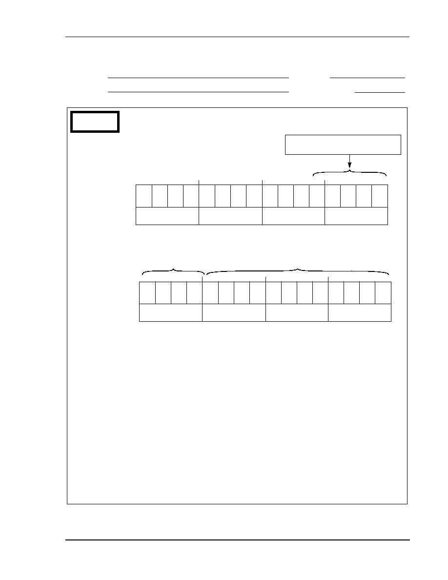
Programmer's Reference
MOTOROLA
DSP56602 User's Manual
D-31
Bus Control
X:$FFFA
Reset = $001F
Register (BCR)
CPU
* = Reserved, Program as 0
BMW4 BMW3
BMW0
BMW1
BMW2
Wait state field for external memory,
binary encoded
$0
*
0
15
6
5
4
3
2
1
0
10
9
8
7
14
13
12
11
*
0
*
0
*
0
*
0
*
0
*
0
*
0
*
0
*
0
*
0
$0
DSP56602
X:$FFF9
Read-Only
Register (IDR)
$1
0
15
6
5
4
3
2
1
0
10
9
8
7
14
13
12
11
0
0
0
1
0
1
1
0
0
0
$6
0
0
0
1
0
$0
$2
Revision
Device Number
Identification
Sheet 6 of 8
Application:
Date:
Programmer:
AA1106f

D-32
DSP56602 User's Manual
MOTOROLA
Programmer's Reference
Patch Register 0
X:$FFF8
Reset =
(PAR0)
PAR
PAR
PAR
PAR
PAR
CPU
PAR
PAR
PAR
15
6
5
4
3
2
1
0
10
9
8
7
14
13
12
11
PAR
PAR
PAR
PAR
PAR
PAR
PAR
PAR
15
14
13
12
11
10
9
8
7
6
5
4
3
2
1
0
Patch Register 1
X:$FFF7
Reset =
(PAR1)
PAR
PAR
PAR
PAR
PAR
PAR
PAR
PAR
15
6
5
4
3
2
1
0
10
9
8
7
14
13
12
11
PAR
PAR
PAR
PAR
PAR
PAR
PAR
PAR
15
14
13
12
11
10
9
8
7
6
5
4
3
2
1
0
Patch Register 3
X:$FFF5
Reset =
(PAR3)
PAR
PAR
PAR
PAR
PAR
PAR
PAR
PAR
15
6
5
4
3
2
1
0
10
9
8
7
14
13
12
11
PAR
PAR
PAR
PAR
PAR
PAR
PAR
PAR
15
14
13
12
11
10
9
8
7
6
5
4
3
2
1
0
Patch Register 2
X:$FFF6
Reset =
(PAR2)
PAR
PAR
PAR
PAR
PAR
PAR
PAR
PAR
15
6
5
4
3
2
1
0
10
9
8
7
14
13
12
11
PAR
PAR
PAR
PAR
PAR
PAR
PAR
PAR
15
14
13
12
11
10
9
8
7
6
5
4
3
2
1
0
uninitialized
uninitialized
uninitialized
uninitialized
Sheet 7 of 8
Application:
Date:
Programmer:
AA1106g
Programmer's Reference
MOTOROLA
DSP56602 User's Manual
D-33
BPMR
BPMR
BPMR
BPMR BPMR
CPU
BPMR BPMR BPMR
15
6
5
4
3
2
1
0
10
9
8
7
14
13
12
11
BPMR
BPMR
BPMR
BPMR
BPMR
BPMR BPMR
BPMR
G15
G14
G13
G12
G11
G10
G9
G8
G7
G6
G5
G4
G3
G2
G1
G0
BPMR
BPMR
BPMR
BPMR BPMR
BPMR BPMR BPMR
15
6
5
4
3
2
1
0
10
9
8
7
14
13
12
11
BPMR
BPMR
BPMR
BPMR
BPMR
BPMR BPMR
BPMR
L15
L14
L13
L12
L11
L10
L9
L8
L7
L6
L5
L4
L3
L2
L1
L0
BPMR BPMR
15
6
5
4
3
2
1
0
10
9
8
7
14
13
12
11
BPMR
BPMR
BPMR
BPMR BPMR
BPMR
H7
H6
H5
H4
H3
H2
H1
H0
*
0
*
0
*
0
*
0
*
0
*
0
*
0
*
0
* = Reserved, Program as 0
$0
$0
Bus Switch
Program Memory
Register Low
(BPMRL)
X:$FFF3
Reset = uninitialized
Bus Switch
Program Memory
Register High
(BPMRH)
X:$FFF2
Reset = $0000
Bus Switch
Program Memory
Register (BPMRG)
X:$FFF4
Reset = uninitialized
Sheet 8 of 8
Application:
Date:
Programmer:
AA1106h

D-34
DSP56602 User's Manual
MOTOROLA
Programmer's Reference
PLL Control
X:$FFFD
Reset = $0000
Register 0 (PCTL0)
MF7
MF8
MF6
MF10
MF9
PLL
PD2
PD1
PD0
COD
DF2
PEN
PD5
PD4
XTLR
DF1
PLL Control
X:$FFFC
Reset = $0000
Register 1 (PCTL1)
PD6
PSTP
Predivider Factor
Use with PD4≠PD6
in PCTL1
$0
*
0
15
6
5
4
3
2
1
0
10
9
8
7
14
13
12
11
15
6
5
4
3
2
1
0
10
9
8
7
14
13
12
11
*
0
*
0
*
0
PEN
Description
0
PLL disabled
1
PLL enabled
*
0
* = Reserved, Program as 0
XTLD
PD3
MF11
MF1
MF2
MF0
MF4
MF3
MF5
Multiplication Factor
DF0
PSTP
Description
0
PLL disabled during Stop state
1
PLL operates during Stop state
XTLD
Description
0
XTAL output enabled
1
XTAL output disabled
(XTAL pin pulled high)
XTLR
Description
0
Use for external crystal
frequency above 200 KHz
1
Use for external crystal
frequency below 200 KHz
Division Factor
Predivider Factor
COD
Description
0
PLL disabled during Stop state
1
PLL operates during Stop state
Use with PD0≠PD3
in PCTL0
Sheet 1 of 1
Application:
Date:
Programmer:
AA1107

Programmer's Reference
MOTOROLA
DSP56602 User's Manual
D-35
HI08
HF3 HF2
HTIE HRIE
Register (HCR)
X:$FFC2
Reset = $0000
Read/Write
15
6
5
4
3
2
1
0
10
9
8
7
14
13
12
11
15
6
5
4
3
2
1
0
10
9
8
7
14
13
12
11
HRDF
Description
0
HRX register is not full
1
HRX register is full
HI08 Status
Register (HSR)
X:$FFC3
Reset = $0002
HI08 Control
*
0
*
0
*
0
*
0
*
0
*
0
*
0
*
0
*
0
*
0
*
0
HF0 HCP
HT
HR
DF
DE
HF1
*
0
*
0
*
0
*
0
*
0
*
0
*
0
*
0
*
0
*
0
*
0
* = Reserved, Program as 0
$0
$0
$0
$0
$0
HTDE
Description
0
HRX register is not empty
1
HTX register is empty
HCP
Description
0
Host Command Interrupt is not
pending (HC bit in CVR is cleared)
1
Host Command Interrupt is
pending (HC bit in CVR is set)
HF0, HF1
General purpose flags.
Values reflect HF0, HF1 in ICR on host side.
HTIE
Description
0
Host Transmit Data Interrupt disabled
1
Host Transmit Data Interrupt enabled
HRIE
Description
0
Host Receive Data Interrupt disabled
1
Host Receive Data Interrupt enabled
HF2, HF3
General purpose flags.
Values reflect HF2, HF3 in ISR on host side
HCIE
HCIE
Description
0
Host Command Interrupt disabled
1
Host Command Interrupt enabled
Read-Only
Sheet 1 of 5
Application:
Date:
Programmer:
AA1108a

D-36
DSP56602 User's Manual
MOTOROLA
Programmer's Reference
HROD
HEN
HASP HDSP
HRP
HAP
HMUX
HAEN HREN
HC
HA9
HA8
HGEN
HI08 Port Control
Register (HPCR)
X:$FFC4
Reset = $0000
HCSP HDDS
15
6
5
4
3
2
1
0
10
9
8
7
14
13
12
11
HEN
Description
0
HI08 disabled
1
HI08 enabled
HASP
Description
0
HAS pin active low
1
HAS pin active high
HDDS
Description
0
Single strobe bus mode
1
Dual strobe bus mode
HCSP
Description
0
HCS pin active low
1
HCS pin active high
HRP
Description
0
HREQ pin (or HTRQ and
HRRQ pins) active low
1
HREQ pin (or HTRQ and
HRRQ pins) active high
HAP
Description
0
HACK pin active low
1
HACK pin active high
HREN
Description
0
HREQ/HTRQ and HACK/HRRQ
used for GPIO
1
HREQ/HTRQ and HACK/HRRQ
enabled (mode-dependent)
HAEN
Description
0
HACK pin configured as GPIO
1
HACK pin is Host Acknowledge input
HGEN
Description
0
Disconnects pins configured
for GPIO
1
Enables pins configured for
GPIO
HCSEN
Description
0
HCS/HA10 used for GPIO
1
HCS/HA10 enabled
HA9EN
Description
0
HA9 used for GPIO
1
HA9 enabled
HA8EN
Description
0
HA8 used for GPIO
1
HA8 enabled
HI08
*
0
SEN
EN
EN
* = Reserved, Program as 0
Read/Write
HROD
Description
0
HREQ pin not open drain
1
HREQ pin is open drain
HMUX
Description
0
HI08 uses non-multiplexed bus
1
HI08 non-multiplexed bus
HDSP
Description
0
Data strobe pins active low
1
Data strobe pins active high
Sheet 2 of 5
Application:
Date:
Programmer:
AA1108b

Programmer's Reference
MOTOROLA
DSP56602 User's Manual
D-37
HI08
HI08 Data Direction
X:$FFC8
Reset = $0000
Register (HDDR)
DR11
DR12
DR10
DR14
DR13
DR15
DR9
DR2
DR3
DR1
DR5
DR4
DR8
DR7
DR6
DR0
15
6
5
4
3
2
1
0
10
9
8
7
14
13
12
11
DRn
Description
0
Pin used for input
1
Pin used for output
Read/Write
HI08 Data
X:$FFC9
Reset = $0000
Register (HDR)
D11
D12
D10
D14
D13
D15
D9
D2
D3
D1
D5
D4
D8
D7
D6
D0
15
6
5
4
3
2
1
0
10
9
8
7
14
13
12
11
Read/Write
HI08 Receive Data
X:$FFC6
Reset = $0000
Register (HRX)
Data
Data
Data
Data
Data
Data
Data
Data
Data
Data
Data
Data
Data
Data
Data
Data
15
6
5
4
3
2
1
0
10
9
8
7
14
13
12
11
Read-Only
HI08 Transmit Data
X:$FFC7
Reset = $0000
Register (HTX)
Data
Data
Data
Data
Data
Data
Data
Data
Data
Data
Data
Data
Data
Data
Data
Data
15
6
5
4
3
2
1
0
10
9
8
7
14
13
12
11
Write-Only
* = Reserved, Program as 0
HI08 Base Address
X:$FFC5
Reset = $0080
Register (HBAR)
BA5
BA6
BA4
BA8
BA7
BA10
BA9
BA3
15
6
5
4
3
2
1
0
10
9
8
7
14
13
12
11
Read/Write
*
0
*
0
*
0
*
0
*
0
*
0
*
0
*
0
$0
$0
Sheet 3 of 5
Application:
Date:
Programmer:
AA1108c

D-38
DSP56602 User's Manual
MOTOROLA
Programmer's Reference
HI08
* = Reserved, Program as 0
Interface Status
Reset = $06
Register (ISR)
TRDY
HF2
TXDE
HF3
HREQ
RXDF
6
5
4
3
2
1
0
7
Read Only
*
0
*
0
HREQ
Description
0
HREQ is deasserted
1
If enabled, HREQ is asserted
TRDY
Description
0
Transmit FIFO is empty
1
Transmit FIFO contains data
HF2, HF3
General purpose flags, values reflect
HF2, HF3 in HCR on DSP side
TXDE
Description
0
HTX register is full
1
HTX register is empty
RXDF
Description
0
HRX register is empty
1
HRX register is full
Interface Control
Reset = $00
Register (ICR)
HDRQ
HF0
TREQ
HL
HF1
INIT
RREQ
6
5
4
3
2
1
0
7
Read/Write
END
*
0
HF0, HF1
General purpose flags, values reflect
HF0, HF1 in HSR on DSP side
HLEND
Description
0
Data accessed "big end" first
1
Data accessed "little end" first
TREQ
Description
0
HACK or TRQ disabled
1
HACK or TRQ enabled
RREQ
Description
0
HREQ or RRQ disabled
1
HRRQ or RRQ enabled
HDRQ
Description
0
HREQ and HACK selected
1
TRQ and RRQ selected
INIT
See Table 7-10 on page 7-25
Sheet 4 of 5
Application:
Date:
Programmer:
AA1108d

Programmer's Reference
MOTOROLA
DSP56602 User's Manual
D-39
HI08
HV2
HV3
HV1
HV5
HV4
HC
HV6
HV0
6
5
4
3
2
1
0
7
Control Vector
Reset = $32
Register (CVR)
Read/Write
HV0≠HV6
Equals VBA register interrupt vector ˜ 2
HC
Description
0
No host command pending
1
Host command is pending
IV2
IV3
IV1
IV5
IV4
IV7
IV6
IV0
6
5
4
3
2
1
0
7
Interrupt Vector
Reset = $0F
Register (IVR)
Read/Write
IV0≠IV7
Contains interrupt vector for MC68000 family
Sheet 5 of 5
Application:
Date:
Programmer:
AA1108e

D-40
DSP56602 User's Manual
MOTOROLA
Programmer's Reference
* = Reserved, Program as 0
PSR
PM0
WL1
PM2
PM1
PM6
PM7
PM3
WL0
DC4
DC3
DC2
DC1
DC0
SSI 0 Control
Register A (CRA0)
X:$FFB6
Reset = $0000
PM5
PM4
15
6
5
4
3
2
1
0
10
9
8
7
14
13
12
11
WL1
WL0
Description
0
0
8 bits per word
0
1
12 bits per word
1
0
16 bits per word
1
1
(Reserved)
TE
TIE
RE
TEIE
REIE
RIE
OF1
OF0
SSI 0 Control
Register B (CRB0)
X:$FFB7
Reset = $0000
RLIE
TLIE
15
6
5
4
3
2
1
0
10
9
8
7
14
13
12
11
*
0
*
0
*
0
*
0
*
0
*
0
$0
Serial Output Flags
Frame Rate Divider Bits
binary encoded
Prescale Modulus Bits
binary encoded
REIE
Description
0
(Bit is cleared)
1
TX Underrun Occurred
TEIE
Description
0
(Bit is cleared)
1
TX Underrun Occurred
RLIE
Description
0
(Bit is cleared)
1
TX Underrun Occurred
TIE
Description
0
Transmit Interrupt disabled
1
Transmit Interrupt enabled
RE
Description
0
Receive disabled
1
Receive enabled
TE
Description
0
Transmit disabled
1
Transmit enabled
TLIE
Description
0
(Bit is cleared)
1
TX Underrun Occurred
RIE
Description
0
Receive Interrupt disabled
1
Receive Interrupt enabled
Read/Write
Read/Write
SSI0
Sheet 1 of 4
Application:
Date:
Programmer:
AA1109a

Programmer's Reference
MOTOROLA
DSP56602 User's Manual
D-41
SSI0
SCD2
CKP
SCKD
FSR
FSP
SHFD
MOD
SYN
SSI 0 Control
Register C (CRC0)
X:$FFB8
Reset = $0000
FSL1
FSL0
15
6
5
4
3
2
1
0
10
9
8
7
14
13
12
11
*
0
*
0
*
0
*
0
$0
SCD1 SCD0
SCD0
Description
0
SC0 pin is input
1
SC0 pin is output
MOD
Description
0
Normal mode selected
1
Network mode selected
SCD1
Description
0
SC1 pin is input
1
SC1 pin is output
SCD2
Description
0
SC2 pin is input
1
SC2 pin is output
SCKD
Description
0
External clock source
1
Internal clock source
CKP
Description
0
Data clocked out on rising edge of TX
clock, latched in on falling edge of RX clock
1
Data clocked out on falling edge of TX
clock, latched in on rising edge of RX clock
* = Reserved, Program as 0
SYN
Description
0
Asynchronous mode
selected
1
Synchronous mode
selected
SHFD
Description
0
Data shifted out MSB first
1
Data shifted out LSB first
FSL1 FSL0
Description
0
0
WL bit clock for both TX and RX
0
1
One-bit clock for TX
WL bit clock for RX
1
0
One-bit clock for both TX and RX
1
1
WL bit clock for TX
One-bit clock for RX
FSR
Description
0
Frame synch occurs with
first bit of current word
1
Frame synch occurs with
last bit of previous word
FSP
Description
0
Positive frame synch
1
Negative frame synch
Sheet 2 of 4
Application:
Date:
Programmer:
AA1109b

D-42
DSP56602 User's Manual
MOTOROLA
Programmer's Reference
* = Reserved, Program as 0
SSI 0 Transmit
Register (TX0)
X:$FFBC
Write-Only
High Byte
15
6
5
4
3
2
1
0
10
9
8
7
14
13
12
11
Low Byte
SSI 0 Receive
Register (RX0)
X:$FFBA
Read-Only
High Byte
15
6
5
4
3
2
1
0
10
9
8
7
14
13
12
11
Low Byte
SSI0
SSI 0 Time Slot
Register (TSR0)
X:$FFBB
Write-Only
Dummy Register, Written During Inactive Time Slots
15
6
5
4
3
2
1
0
10
9
8
7
14
13
12
11
TUE
Description
0
(Bit is cleared)
1
TX Underrun Occurred
RDF
TDE
ROE
TUE
RFS
TFS
IF1
IF0
*
0
15
6
5
4
3
2
1
0
10
9
8
7
14
13
12
11
* = Reserved, Program as 0
*
0
*
0
*
0
*
0
*
0
*
0
*
0
$0
$0
SSI 0 Status
Register (SSISR0)
X:$FFB9
Reset = $0040
RDF
Description
0
(Bit is cleared)
1
RX Data Register has data
TDE
Description
0
(Bit is cleared)
1
TX Data Register Empty
ROE
Description
0
(Bit is cleared)
1
RX Overrun Occurred
TFS
Description
0
No Frame Sync
1
TX Frame Sync Occurred
RFS
Description
0
No Frame Sync
1
RX Frame Sync Occurred
Serial
Input Flags
Sheet 3 of 4
Application:
Date:
Programmer:
AA1109c

Programmer's Reference
MOTOROLA
DSP56602 User's Manual
D-43
SSI0
* = Reserved, Program as 0
SSI 0 Port C Control
X:$FFBF
Reset = $0000
Register (PCRC)
PC2
PC3
PC1
PC5
PC4
PEN
PC0
15
6
5
4
3
2
1
0
10
9
8
7
14
13
12
11
PCn
Description
0
Pin is GPIO pin
1
Pin is SSI pin
SSI 0 Port C
X:$FFBE
Reset = $0000
Register (PRRC)
PDC2
PDC3
PDC1
PDC5 PDC4
PDC0
PD2
PD3
PD1
PD5
PD4
PD0
15
6
5
4
3
2
1
0
10
9
8
7
14
13
12
11
15
6
5
4
3
2
1
0
10
9
8
7
14
13
12
11
Data Direction
SSI 0 Port C Data
X:$FFBD
Reset = $0000
Register (PDRC)
Read/Write
*
0
*
0
*
0
*
0
$0
*
0
*
0
*
0
*
0
$0
*
0
PEN
Description
0
SSI pins tri-stated
1
SSI pins enabled
PDn
Description
0
Pin is input
1
Pin is output
*
0
*
0
*
0
*
0
$0
*
0
*
0
*
0
*
0
$0
*
0
*
0
Read/Write
*
0
*
0
*
0
*
0
$0
*
0
*
0
*
0
*
0
$0
*
0
*
0
Read/Write
Sheet 4 of 4
Application:
Date:
Programmer:
AA1109d

D-44
DSP56602 User's Manual
MOTOROLA
Programmer's Reference
* = Reserved, Program as 0
PSR
PM0
WL1
PM2
PM1
PM6
PM7
PM3
WL0
DC4
DC3
DC2
DC1
DC0
SSI 1 Control
Register A (CRA1)
X:$FFA6
Reset = $0000
PM5
PM4
15
6
5
4
3
2
1
0
10
9
8
7
14
13
12
11
SSI1
WL1
WL0
Description
0
0
8 bits per word
0
1
12 bits per word
1
0
16 bits per word
1
1
(Reserved)
TE
TIE
RE
TEIE
REIE
RIE
OF1
OF0
SSI 1 Control
Register B (CRB1)
X:$FFA7
Reset = $0000
RLIE
TLIE
15
6
5
4
3
2
1
0
10
9
8
7
14
13
12
11
*
0
*
0
*
0
*
0
*
0
*
0
$0
Serial Output Flags
Frame Rate Divider Bits
binary encoded
Prescale Modulus Bits
binary encoded
REIE
Description
0
(Bit is cleared)
1
TX Underrun Occurred
TEIE
Description
0
(Bit is cleared)
1
TX Underrun Occurred
RLIE
Description
0
(Bit is cleared)
1
TX Underrun Occurred
TIE
Description
0
Transmit Interrupt disabled
1
Transmit Interrupt enabled
RE
Description
0
Receive disabled
1
Receive enabled
TE
Description
0
Transmit disabled
1
Transmit enabled
TLIE
Description
0
(Bit is cleared)
1
TX Underrun Occurred
RIE
Description
0
Receive Interrupt disabled
1
Receive Interrupt enabled
Read/Write
Read/Write
Sheet 1 of 4
Application:
Date:
Programmer:
AA1110a

Programmer's Reference
MOTOROLA
DSP56602 User's Manual
D-45
SSI1
SCD2
CKP
SCKD
FSR
FSP
SHFD
MOD
SYN
SSI 1 Control
Register C (CRC1)
X:$FFA8
Reset = $0000
FSL1
FSL0
15
6
5
4
3
2
1
0
10
9
8
7
14
13
12
11
*
0
*
0
*
0
*
0
$0
SCD1 SCD0
SCD0
Description
0
SC0 pin is input
1
SC0 pin is output
MOD
Description
0
Normal mode selected
1
Network mode selected
SCD1
Description
0
SC1 pin is input
1
SC1 pin is output
SCD2
Description
0
SC2 pin is input
1
SC2 pin is output
SCKD
Description
0
External clock source
1
Internal clock source
CKP
Description
0
Data clocked out on rising edge of TX
clock, latched in on falling edge of RX clock
1
Data clocked out on falling edge of TX
clock, latched in on rising edge of RX clock
* = Reserved, Program as 0
SYN
Description
0
Asynchronous mode
selected
1
Synchronous mode
selected
SHFD
Description
0
Data shifted out MSB first
1
Data shifted out LSB first
FSR
Description
0
Frame synch occurs with
first bit of current word
1
Frame synch occurs with
last bit of previous word
FSP
Description
0
Positive frame synch
1
Negative frame synch
FSL1 FSL0
Description
0
0
WL bit clock for both TX and RX
0
1
One-bit clock for TX
WL bit clock for RX
1
0
One-bit clock for both TX and RX
1
1
WL bit clock for TX
One-bit clock for RX
Sheet 2 of 4
Application:
Date:
Programmer:
AA1110b

D-46
DSP56602 User's Manual
MOTOROLA
Programmer's Reference
* = Reserved, Program as 0
SSI 1 Transmit
Register (TX1)
X:$FFAC
Write-Only
High Byte
15
6
5
4
3
2
1
0
10
9
8
7
14
13
12
11
Low Byte
SSI 1 Receive
Register (RX1)
X:$FFAA
Read-Only
High Byte
15
6
5
4
3
2
1
0
10
9
8
7
14
13
12
11
Low Byte
SSI1
SSI 1 Time Slot
Register (TSR1)
X:$FFAB
Write-Only
Dummy Register, Written During Inactive Time Slots
15
6
5
4
3
2
1
0
10
9
8
7
14
13
12
11
TUE
Description
0
(Bit is cleared)
1
TX Underrun Occurred
RDF
TDE
ROE
TUE
RFS
TFS
IF1
IF0
*
0
15
6
5
4
3
2
1
0
10
9
8
7
14
13
12
11
* = Reserved, Program as 0
*
0
*
0
*
0
*
0
*
0
*
0
*
0
$0
$0
SSI 1 Status
Register (SSISR1)
X:$FFA9
Reset = $0040
RDF
Description
0
(Bit is cleared)
1
RX Data Register has data
TDE
Description
0
(Bit is cleared)
1
TX Data Register Empty
ROE
Description
0
(Bit is cleared)
1
RX Overrun Occurred
TFS
Description
0
No Frame Sync
1
TX Frame Sync Occurred
RFS
Description
0
No Frame Sync
1
RX Frame Sync Occurred
Serial
Input Flags
Sheet 3 of 4
Application:
Date:
Programmer:
AA1110c

Programmer's Reference
MOTOROLA
DSP56602 User's Manual
D-47
SSI1
* = Reserved, Program as 0
SSI 1 Port D Control
X:$FFAF
Reset = $0000
Register (PCRD)
PC2
PC3
PC1
PC5
PC4
PEN
PC0
15
6
5
4
3
2
1
0
10
9
8
7
14
13
12
11
PCn
Description
0
Pin is GPIO pin
1
Pin is SSI pin
SSI 1 Port D
X:$FFAE
Reset = $0000
Register (PRRD)
PDC2
PDC3
PDC1
PDC5 PDC4
PDC0
PD2
PD3
PD1
PD5
PD4
PD0
15
6
5
4
3
2
1
0
10
9
8
7
14
13
12
11
15
6
5
4
3
2
1
0
10
9
8
7
14
13
12
11
Data Direction
SSI 1 Port D Data
X:$FFAD
Reset = $0000
Register (PDRD)
Read/Write
*
0
*
0
*
0
*
0
$0
*
0
*
0
*
0
*
0
$0
*
0
PEN
Description
0
SSI pins tri-stated
1
SSI pins enabled
PDn
Description
0
Pin is input
1
Pin is output
*
0
*
0
*
0
*
0
$0
*
0
*
0
*
0
*
0
$0
*
0
*
0
Read/Write
*
0
*
0
*
0
*
0
$0
*
0
*
0
*
0
*
0
$0
*
0
*
0
Read/Write
Sheet 4 of 4
Application:
Date:
Programmer:
AA1110d

D-48
DSP56602 User's Manual
MOTOROLA
Programmer's Reference
GPIO
* = Reserved, Program as 0
GPIO Port E Control
X:$FF9F
Reset = $0000
Register (PCRE)
PC2
PC1
PC0
15
6
5
4
3
2
1
0
10
9
8
7
14
13
12
11
X:$FF9E
Reset = $0000
Register (PRRE)
PDC2 PDC1 PDC0
PD2
PD1
PD0
15
6
5
4
3
2
1
0
10
9
8
7
14
13
12
11
15
6
5
4
3
2
1
0
10
9
8
7
14
13
12
11
GPIO Port E Direction
GPIO Port E Data
X:$FF9D
Reset = $0007
Register (PDRE)
Read/Write
*
0
*
0
*
0
*
0
$0
*
0
*
0
*
0
*
0
$0
PCn
PDCn
Port Pin Function
0
0
GPIO input
0
1
GPIO output
1
0
tri-stated
1
1
GPIO output, open-drain
*
0
*
0
*
0
*
0
$0
*
0
*
0
*
0
*
0
$0
Read/Write
*
0
*
0
*
0
*
0
$0
*
0
*
0
*
0
*
0
$0
Read/Write
*
0
*
0
*
0
*
0
$0
*
0
*
0
*
0
*
0
*
0
$0
*
0
*
0
*
0
*
0
*
0
$0
*
0
Sheet 1 of 1
Application:
Date:
Programmer:
AA1111

Programmer's Reference
MOTOROLA
DSP56602 User's Manual
D-49
Timers
* = Reserved, Program as 0
Timer Prescaler
Load Register
Reset = $0000
Read/Write
15
6
5
4
3
2
1
0
10
9
8
7
14
13
12
11
15
6
5
4
3
2
1
0
10
9
8
7
14
13
12
11
X:$FF83
(TPLR)
PS1
PS0
PL13
PL12
PL11
PL10
PL9
PL8
PL7
PL6
PL5
PL4
PL3
PL2
PL1
PL0
PC13
PC12
PC11
PC10
PC9
PC8
PC7
PC6
PC5
PC4
PC3
PC2
PC1
PC0
*
0
*
0
Timer Prescaler
Count Register
Reset = uninitialized
Read-Only
X:$FF82
(TPCR)
PS1
PS0
Prescaler Clock Source
0
0
Internal Clock ˜ 2
0
1
TIO0
1
0
TIO1
1
1
TIO2
PC0≠PC13
Prescaler count value
PL0≠PL13
Prescaler load value
Sheet 1 of 4
Application:
Date:
Programmer:
AA1112a

D-50
DSP56602 User's Manual
MOTOROLA
Programmer's Reference
Timer0
* = Reserved, Program as 0
TE
Description
0
Timer disabled
1
Timer enabled
TOIE
Description
0
Timer Overflow Interrupt disabled
1
Timer Overflow Interrupt enabled
INV
Description
0
Timer increments on rising transitions
1
Timer increments on falling transitions
See Inverter Bit (INV)--Bit 8 on page 9-11 for
more information.
Timer 0 Control/
X:$FF8F
Reset = $0000
(TCSR0)
TC3
TC2
TE
TCIE
TOIE
TC0
INV
DI
DO
PCE
TRM
DIR
Status Register
15
6
5
4
3
2
1
0
10
9
8
7
14
13
12
11
Read/Write
TOF
TCF
TC1
*
0
TCIE
Description
0
Timer Compare Interrupt disabled
1
Timer Compare Interrupt enabled
TRM
Description
0
Timer is free-running
1
Timer reloads when TCR
value is reached
See Data Input
Bit (DI)--Bit 11
on page 9-11
TOF
Description
0
(bit is cleared)
1
Timer Overflow detected
TCF
Description
0
(bit is cleared)
1
Timer has reached
value in TCR
PCE
Description
0
Prescaler disabled
1
Prescaler enabled
DIR
Description
0
TIO pin is input
1
TIO pin is output
See Data Output
Bit (DO)--Bit 12
on page 9-12
Timer 0 Load
X:$FF8E
Register (TLR0)
Reset = Uninitialized
Write-Only
15
6
5
4
3
2
1
0
10
9
8
7
14
13
12
11
Timer 0 Compare
X:$FF8D
Register (TCPR0)
15
6
5
4
3
2
1
0
10
9
8
7
14
13
12
11
Reset = Uninitialized
Read/Write
Timer 0 Count
X:$FF8C
Register (TCR0)
15
6
5
4
3
2
1
0
10
9
8
7
14
13
12
11
Reset = $0000
Read-Only
Timer Mode
Control Bits
See Table 9-2
on page 9-10
Sheet 2 of 4
Application:
Date:
Programmer:
AA1112b

Programmer's Reference
MOTOROLA
DSP56602 User's Manual
D-51
Timer1
TE
Description
0
Timer disabled
1
Timer enabled
TOIE
Description
0
Timer Overflow Interrupt disabled
1
Timer Overflow Interrupt enabled
INV
Description
0
Timer increments on rising transitions
1
Timer increments on falling transitions
See Inverter Bit (INV)--Bit 8 on page 9-11 for
more information.
Timer 1 Control/
X:$FF8B
Reset = $0800
(TCSR1)
TC3
TC2
TE
TCIE
TOIE
TC0
INV
DI
DO
PCE
TRM
DIR
Status Register
15
6
5
4
3
2
1
0
10
9
8
7
14
13
12
11
Read/Write
TOF
TCF
TC1
*
0
TCIE
Description
0
Timer Compare Interrupt disabled
1
Timer Compare Interrupt enabled
TRM
Description
0
Timer is free-running
1
Timer reloads when TCR
value is reached
See Data Input
Bit (DI)--Bit 11
on page 9-11
TOF
Description
0
(bit is cleared)
1
Timer Overflow detected
TCF
Description
0
(bit is cleared)
1
Timer has reached
value in TCR
PCE
Description
0
Prescaler disabled
1
Prescaler enabled
DIR
Description
0
TIO pin is input
1
TIO pin is output
See Data Output
Bit (DO)--Bit 12
on page 9-12
* = Reserved, Program as 0
Timer 1 Load
X:$FF8A
Register (TLR1)
Reset = Uninitialized
Write-Only
15
6
5
4
3
2
1
0
10
9
8
7
14
13
12
11
Timer 1 Compare
X:$FF89
Register (TCPR1)
15
6
5
4
3
2
1
0
10
9
8
7
14
13
12
11
Reset = Uninitialized
Read/Write
Timer 1 Count
X:$FF88
Register (TCR1)
15
6
5
4
3
2
1
0
10
9
8
7
14
13
12
11
Reset = $0000
Read-Only
Timer Mode
Control Bits
See Table 9-2
on page 9-10
Sheet 3 of 4
Application:
Date:
Programmer:
AA1112c

D-52
DSP56602 User's Manual
MOTOROLA
Programmer's Reference
Timer2
TE
Description
0
Timer disabled
1
Timer enabled
TOIE
Description
0
Timer Overflow Interrupt disabled
1
Timer Overflow Interrupt enabled
INV
Description
0
Timer increments on rising transitions
1
Timer increments on falling transitions
See Inverter Bit (INV)--Bit 8 on page 9-11 for
more information.
Timer 2 Control/
X:$FF87
Reset = $0800
(TCSR2)
TC3
TC2
TE
TCIE
TOIE
TC0
INV
DI
DO
PCE
TRM
DIR
Status Register
15
6
5
4
3
2
1
0
10
9
8
7
14
13
12
11
Read/Write
TOF
TCF
TC1
*
0
TCIE
Description
0
Timer Compare Interrupt disabled
1
Timer Compare Interrupt enabled
TRM
Description
0
Timer is free-running
1
Timer reloads when TCR
value is reached
See Data Input
Bit (DI)--Bit 11
on page 9-11
TOF
Description
0
(bit is cleared)
1
Timer Overflow detected
TCF
Description
0
(bit is cleared)
1
Timer has reached
value in TCR
PCE
Description
0
Prescaler disabled
1
Prescaler enabled
DIR
Description
0
TIO pin is input
1
TIO pin is output
See Data Output
Bit (DO)--Bit 12
on page 9-12
* = Reserved, Program as 0
Timer 2 Load
X:$FF86
Register (TLR2)
Reset = Uninitialized
Write-Only
15
6
5
4
3
2
1
0
10
9
8
7
14
13
12
11
Timer 2 Compare
X:$FF85
Register (TCPR2)
15
6
5
4
3
2
1
0
10
9
8
7
14
13
12
11
Reset = Uninitialized
Read/Write
Timer 2 Count
X:$FF84
Register (TCR2)
15
6
5
4
3
2
1
0
10
9
8
7
14
13
12
11
Reset = $0000
Read-Only
Timer Mode
Control Bits
See Table 9-2
on page 9-10
Sheet 4 of 4
Application:
Date:
Programmer:
AA1112d

MOTOROLA
DSP56602 User's Manual
Index-1
INDEX
A
A0≠A15 signals
2-10
adder
modulo
1-8
offset
1-8
reverse-carry
1-8
Address Bus Ground signal (GND
A
)
2-6
Address Bus Power signal (V
CCA
)
2-5
Address Bus signals (A0≠A15)
2-10
Address Bus--A0≠A15
5-3
address generation unit
1-8
Address Trace Enable bit (ATE)
4-6
Address Trace signal (AT)
2-11
,
5-4
Address Tracing (AT) mode
5-10
AGU
1-8
Asynchronous/Synchronous bit (SYN)
8-14
AT mode
5-10
AT signal
2-11
,
5-4
ATE bit
4-6
B
BA3≠BA10 bits
7-17
Base Address bits (BA3≠BA10)
7-17
BCR register
4-8
,
5-7
bits 0≠4--Expansion Bus Memory Wait bits
(BMW0≠BMW4)
5-7
reserved bits--bits 5≠15
5-8
BMPR register
5-8
BMW0≠BMW4 bits
5-7
Boundary Scan Register (BSR)
11-7
BPMR register
16-bit access
5-9
24-bit access
5-9
mapping
5-8
typical usage
5-9
Breakpoint 0 and 1 Event bits (BT0≠BT1)
10-14
Breakpoint 0 Condition Code Select bits
(CC00≠CC01)
10-13
Breakpoint 0 Read/Write Select bits
(RW00≠RW01)
10-12
Breakpoint 1 Condition Code Select bits
(CC10≠CC11)
10-14
Breakpoint 1 Read/Write Select bits
(RW10≠RW11)
10-13
BSR bit definitions
11-13
BSR register
11-7
BT0≠BT1 bits
10-14
Bus Control Ground signal (GND
C
)
2-6
Bus Control Power signal (V
CCC
)
2-5
Bus Control Register (BCR)
4-8
,
5-7
Bus Switch Program Memory Register (BPMR)
5-8
buses
internal
1-11
BYPASS instruction
11-12
C
CC00≠CC01 bits
10-13
CC10≠CC11 bits
10-14
CCR register
4-7
Chip Operating Mode bits (MD,MC, MB, and
MA)
4-4
Chip Operating Modes
4-9
CKP bit
8-15
CLAMP instruction
11-10
CLKOUT signal
2-7
Clock Output Disable bit (COD)
4-19
Clock Output signal (CLKOUT)
2-7
Clock Polarity bit (CKP)
8-15
Clock signals
2-7
Clock Source Direction bit (SCKD)
8-15
COD bit
4-19
Command Vector Register (CVR)
7-25
Condition Code Register (CCR)
4-7
configuration
GPIO
6-3
Core Status bits (OS0≠OS1)
10-9
CRA register
8-7
bits 0≠7--Prescale Modulus Select bits
(PM0≠PM7)
8-8
bits 8≠12--Frame Rate Divider Control bits
(DC4≠DC0)
8-8
bits 13≠14--Word Length Control bits
(WL0≠WL1)
8-8
bit 15--Prescaler Range bit (PSR)
8-9
CRB register
bit 0--Serial Output Flag 0 bit (OF0)
8-10
bit 1--Serial Output Flag 1 bit (OF1)
8-10
bit 8--Transmit Enable bit (TE)
8-11
bit 9--Receive Enable bit (RE)
8-12
bit 10--Transmit Interrupt Enable bit
(TIE)
8-12
bit 11--Receive Interrupt Enable bit (RIE)
8-12
bit 12--Transmit Last Slot Interrupt Enable bit
(TLIE)
8-13
bit 13--Receive Last Slot Interrupt Enable bit
(RLIE)
8-13
bit 14--Transmit Exception Interrupt Enable
bit (TEIE)
8-13

D
Index-2
DSP56602 User's Manual
MOTOROLA
bit 15--Receive Exception Interrupt Enable bit
(REIE)
8-13
reserved bits--bits 2≠7
8-10
CRC register
bit 0--Asynchronous/Synchronous bit
(SYN)
8-14
bit 1--SSI Mode Select bit (MOD)
8-14
bit 2--Serial Control 0 Direction bit
(SCD0)
8-14
bit 3--Serial Control 1 Direction bit
(SCD1)
8-14
bit 4--Serial Control 2 Direction bit
(SCD2)
8-15
bit 5--Clock Source Direction bit (SCKD)
8-15
bit 6--Clock Polarity bit (CKP)
8-15
bit 7--Shift Direction bit (SHFD)
8-15
bits 12≠13--Frame Sync Length bits
(FSL1≠FSL0)
8-15
bit 14--Frame Sync Relative Timing bit
(FSR)
8-16
bit 15--Frame Sync Polarity bit (FSP)
8-16
reserved bits--bits 8≠11
8-15
Crystal Output signal (XTAL)
2-7
Crystal Range bit (XTLR)
4-19
CVR register
7-25
bits 0≠6--Host Vector bits (HV0≠HV6)
7-25
bit 7--Host Command bit (HC)
7-26
D
D0≠D23 signals
2-10
data ALU
1-7
Data Bus Ground signal (GND
D
)
2-6
Data Bus Power signal (V
CCD
)
2-5
Data Bus Power signal (V
CCH
)
2-5
Data Bus signals (A0≠A15)
2-10
Data Bus--D0≠D23
5-3
Data Input bit (DI)
9-11
Data Output bit (DO)
9-12
DC4≠DC0 bits
8-8
DE signal
2-26
,
10-4
Debug Event signal (DE signal)
2-26
,
10-4
Debug mode
in OnCE module
10-16
DEBUG_REQUEST instruction
11-11
executing during Stop state
10-17
executing during Wait state
10-17
executing in OnCE module
10-17
Device Identification Register (IDR)
4-8
DF2≠DF0 bits
4-18
DI bit
9-11
DIR bit
9-11
Direction bit (DIR)
9-11
Division Factor bits (DF2≠DF0)
4-18
DO bit
9-12
Double Host Request bit (HDRQ)
7-24
E
EBD bit
4-5
EN bit
4-6
ENABLE_ONCE instruction
11-11
EOV bit
4-6
EUN bit
4-5
EX bit
10-7
Exit Command bit (EX)
10-7
Expanded Mode (Mode 0)
4-10
Expansion Bus Memory Wait bits
(BMW0≠BMW4)
5-7
Expansion Port signals
2-10
Expansion Port, Port A pins
2-10
EXTAL signal
2-7
Extended Stack Enable bit (EN)
4-6
Extended Stack Overflow bit (EOV)
4-6
Extended Stack Underflow bit (EUN)
4-5
Extended Stack Wrap bit (WR)
4-6
External Bus Disable bit (EBD)
4-5
External Clock/Crystal Input signal (EXTAL)
2-7
EXTEST instruction
11-9
F
Frame Rate Divider Control bits (DC4≠DC0)
8-8
Frame Sync Length bits (FSL1≠FSL0)
8-15
Frame Sync Polarity bit (FSP)
8-16
Frame Sync Relative Timing bit (FSR)
8-16
FSL1≠FSL0 bits
8-15
FSP bit
8-16
FSR bit
8-16
G
General Purpose I/O (GPIO) port
6-3
General Purpose I/O 0 signal (GPI00)
2-24
General Purpose I/O 1 signal (GPI01)
2-24
General Purpose I/O 2 signal (GPI02)
2-24
General Purpose I/O signals
2-24
Global Data Bus
1-11
GND
A
signal
2-6

H
MOTOROLA
DSP56602 User's Manual
Index-3
GND
C
signal
2-6
GND
D
signal
2-6
GND
H
signal
2-6
GND
P
signal
2-6
GND
Q
signal
2-6
GND
S
signal
2-6
GO Command bit (GO)
10-7
GPI00 signal
2-24
GPI01 signal
2-24
GPI02 signal
2-24
GPIO
1-13
configuration
6-3
in HI08
7-30
GPIO Control Register (PCRE)
6-5
GPIO Data Register (PDRE)
6-6
GPIO signals
2-24
Ground signals
2-6
H
HA0 signal
2-13
HA1 signal
2-14
HA10 signal
2-16
HA2 signal
2-14
HA8 signal
2-14
HA8EN bit
7-12
HA9 signal
2-14
HA9EN bit
7-12
HACK signal
2-17
HAD0≠HAD7 signals
2-13
HAEN bit
7-13
HAP bit
7-16
Hardware reset signal (RESET)
2-8
HAS signal
2-13
HASP bit
7-14
HBAR register
7-17
bits 0≠7--Base Address bits (BA3≠BA10)
7-17
reserved bits--bits 5≠15
7-17
HC bit
7-26
HCIE bit
7-9
HCP bit
7-11
HCR register
bit 0--Host Receive Interrupt Enable bit
(HRIE)
7-9
bit 1--Host Transmit Interrupt Enable bit
(HTIE)
7-9
bit 2--Host Command Interrupt Enable bit
(HCIE)
7-9
bits 3, 4--Host Flag 2 and 3 bits (HF2,
HF3)
7-10
reserved bits--bits 5≠15
7-10
HCS signal
2-16
HCSEN bit
7-13
HCSP bit
7-15
HD0≠HD7 signals
2-13
HDDR register
7-16
HDDS bit
7-14
HDR register
7-16
HDRQ bit
7-24
HDS signal
2-15
HDSP bit
7-14
HEN bit
7-13
HF0 bit
7-11
,
7-24
HF1 bit
7-11
,
7-24
HF2 bit
7-10
,
7-27
HF3 bit
7-10
,
7-27
HGEN bit
7-12
HI08
data transfer
7-31
polling
7-31
servicing interrupts
7-32
HI08 Base Address Register (HBAR)
7-17
HI08 Control Register (HCR
7-8
HI08 Data Direction Register (HDDR)
7-16
HI08 Data Register (HDR)
7-16
HI08 Receive Data Register (HRX)
7-18
HI08 signals
2-13
HI08 Status Register (HSR)
7-10
HI08 Transmit Data Register (HTX)
7-18
HI-Z instruction
11-11
HLEND bit
7-24
HMUX bit
7-14
Host Acknowledge Enable bit (HAEN)
7-13
Host Acknowledge Polarity bit (HAP)
7-16
Host Acknowledge signal (HACK)
2-17
Host Address 8 signal (HA8)
2-14
Host Address 9 signal (HA8)
2-14
Host Address Bus signals (HAD0≠HAD7)
2-13
Host Address Input 0 signal (HA0)
2-13
Host Address Input 1 signal (HA01)
2-14
Host Address Input 2 signal (HA2)
2-14
Host Address Input 10 signal (HA10)
2-16
Host Address Line 8 Enable bit (HA8EN)
7-12
Host Address Line 9 Enable bit (HA9EN)
7-12
Host Address Strobe Polarity bit (HASP)
7-14
Host Address Strobe signal (HAS)
2-13
Host Chip Select Enable bit (HCSEN)
7-13
Host Chip Select Polarity bit (HCSP)
7-15
Host Chip Select signal (HCS)
2-16
Host Command bit (HC)
7-26
Host Command Interrupt Enable bit (HCIE)
7-9
Host Command Pending bit (HCP)
7-11

I
Index-4
DSP56602 User's Manual
MOTOROLA
Host Data Bus signals (HD0≠HD7)
2-13
Host Data Strobe Polarity bit (HDSP)
7-14
Host Data Strobe signal (HDS)
2-15
Host Dual Data Strobe bit (HDDS)
7-14
Host Enable bit (HEN)
7-13
Host Flag 0 bit (HF0)
7-11
,
7-24
Host Flag 1 bit (HF1)
7-11
,
7-24
Host Flag 2 bit (HF2)
7-10
,
7-27
Host Flag 3 bit (HF3)
7-10
,
7-27
Host GPIO Port Enable bit (HGEN)
7-12
Host Ground signal (GND
H
)
2-6
Host Interface (HI08)
7-3
Host Interface (HI08)'HI08
1-13
Host Interface signals (HI08)
2-13
Host Little Endian bit (HLEND)
7-24
Host Multiplexed Bus bit (HMUX)
7-14
Host Port Control Register (HPCR)
7-12
host port usage
2-12
Host Read Data signal (HRD)
2-15
Host Read/Write signal (HRW)
2-15
Host Receive Data Full bit (HRDF)
7-10
Host Receive Interrupt Enable bit (HRIE)
7-9
Host Request Enable bit (HREN)
7-13
Host Request Open Drain bit (HROD)
7-13
Host Request Polarity bit (HRP)
7-15
Host Request signal (HREQ)
2-16
Host Transmit Data Empty bit (HTDE)
7-11
Host Transmit Interrupt Enable bit (HTIE)
7-9
Host Vector bits (HV0≠HV6)
7-25
Host Write Enable Strobe signal (HWR)
2-15
HPCR register
bit 0--Host GPIO Port Enable bit (HGEN)
7-12
bit 1--Host Address Line 8 bit (HA8EN)
7-12
bit 2--Host Address Line 9 bit (HA9EN)
7-12
bit 3--Host Chip Select Enable bit
(HCSEN)
7-13
bit 4--Host Request Enable bit (HREN)
7-13
bit 5--Host Acknowledge Enable bit
(HAEN)
7-13
bit 6--Host Enable bit (HEN)
7-13
bit 8--Host Request Open Drain bit
(HROD)
7-13
bit 9--Host Data Strobe Polarity bit
(HDSP)
7-14
bit 10--Host Address Strobe Polarity bit
(HASP)
7-14
bit 11--Host Multiplexed Bus bit (HMUX)
7-14
bit 12--Host Dual Data Strobe bit (HDDS)
7-14
bit 13--Host Chip Select Polarity bit
(HCSP)
7-15
bit 14--Host Request Polarity bit (HRP)
7-15
bit 15--Host Acknowledge Polarity bit
(HAP)
7-16
reserved bit--bit 7
7-13
HRD signal
2-15
HRDF bit
7-10
HREN bit
7-13
HREQ bit
7-27
HREQ signal
2-16
HRIE bit
7-9
HROD bit
7-13
HRP bit
7-15
HRRQ signal
2-17
HRW signal
2-15
HRX register
7-18
HSR register
bit 0--Host Receive Data Full bit (HRDF)
7-10
bit 1--Host Transmit Data Empty bit
(HTDE)
7-11
bit 2--Host Command Pending bit (HCP)
7-11
bits 3, 4--Host Flag 0 and 1 bits (HF0,
HF1)
7-11
reserved bits--bits 5≠15
7-11
HTDE bit
7-11
HTIE bit
7-9
HTRQ signal
2-16
HTX register
7-18
HV0≠HV6 bits
7-25
HWR signal
2-15
I
ICR register
7-22
bit 0--Receive Request Enable bit (RREQ)
7-23
bit 1--Transmit Request Enable bit
(TREQ)
7-23
bit 2--Double Host Request bit (HDRQ)
7-24
bit 3--Host Flag 0 bit (HF0)
7-24
bit 4--Host Flag 1 bit (HF1)
7-24
bit 5--Host Little Endian bit (HLEND)
7-24
bit 7--Initialize bit (INIT)
7-24
reserved bit--bit 6
7-25
IDCODE instruction
11-9
IDR register
4-8
IF0 bit
8-17
IF1 bit
8-17
IME bit
10-8

J
MOTOROLA
DSP56602 User's Manual
Index-5
INIT bit
7-24
Initialize bit (INIT)
7-24
input and output signals
2-3
Interface Control Register (ICR)
7-22
Interface Status Register (ISR)
7-26
internal buses
1-11
Interrupt
10-8
Interrupt And Mode Control pins
2-8
Interrupt Control signals
2-8
Interrupt Mode Enable bit (IME)
10-8
Interrupt Priority Levels
4-13
Interrupt Priority Register--Core (IPR-C)
4-13
Interrupt Priority Register--Peripheral
(IPR-P)
4-13
interrupt starting address
4-11
Interrupt Vector Register (IVR)
7-28
INV bit
9-11
Inverter bit (INV)
9-11
IPR-C register
4-13
IPR-P register
4-13
ISR Host Request bit (HREQ)
7-27
ISR register
7-26
bit 0--Receive Data Register Full bit
(RXDF)
7-26
bit 1--Transmit Data Register Empty bit
(TXDE)
7-27
bit 2--Transmitter Ready bit (TRDY)
7-27
bit 3--Host Flag 2 bit (HF2)
7-27
bit 4--Host Flag 3 bit (HF3)
7-27
bit 7--ISR Host Request bit (HREQ)
7-27
reserved bits--bits 5, 6
7-27
IVR register
7-28
J
Joint Test Action Group (JTAG)
11-3
JTAG
1-10
JTAG instructions
BYPASS instruction
11-12
CLAMP instruction
11-10
DEBUG_REQUEST instruction
11-11
ENABLE_ONCE instruction
11-11
EXTEST instruction
11-9
HI-Z instruction
11-11
IDCODE instruction
11-9
SAMPLE/PRELOAD instruction
11-9
JTAG/OnCE Interface signals
2-26
Debug Event signal (DE signal)
2-26
,
10-4
Test Clock signal (TCK)
2-26
Test Data Input signal (TDI)
2-26
Test Data Output signal (TDO)
2-26
Test Mode Select signal (TMS)
2-26
Test Reset signal (TRST)
2-26
L
LA register
1-9
LC register
1-9
Loop Address register (LA)
1-9
Loop Counter register (LC)
1-9
M
MAC
1-7
MBO bit
10-9
MBS0≠MBS1 bits
10-12
MCS signal
2-10
,
5-3
MD,MC, MB, and MA bits
4-4
memory
on-chip
1-11
Memory Breakpoint Occurrence bit (MBO)
10-9
Memory Breakpoint Select bits
(MBS0≠MBS1)
10-12
memory breakpoints
enabling
10-18
Memory Chip Select signal (MCS)
2-10
,
5-3
memory map description
3-3
memory-mapped I/O registers
3-5
MF0≠MF11 bits
4-17
MOD bit
8-14
MODA/IRQA signal
2-8
MODB/IRQB signal
2-9
MODC/IRQC signal
2-9
MODD/IRQD signal
2-10
Mode Control signals
2-8
Mode Register (MR)
4-7
Mode Select A/External Interrupt Request A
signal (MODA/IRQA)
2-8
Mode Select B/External Interrupt Request B signal
(MODA/IRQB)
2-9
Mode Select C/External Interrupt Request C signal
(MODC/IRQC)
2-9
Mode Select D/External Interrupt Request D
signal (MODD/IRQD)
2-10
modulo adder
1-8
MR register
4-7
Multiplication Factor bits (MF0≠MF11)
4-17
multiplier-accumulator
1-7
N
Normal mode
4-10

O
Index-6
DSP56602 User's Manual
MOTOROLA
O
OBCR register
10-12
bits 0≠1--Memory Breakpoint Select bits
(MBS0≠MBS1)
10-12
bits 2≠3--Breakpoint 0 Read/Write Select bits
(RW00≠RW01)
10-12
bits 4≠5--Breakpoint 0 Condition Code Select
bits (CC00≠CC01)
10-13
bits 6≠7--Breakpoint 1 Read/Write Select bits
(RW10≠RW11)
10-13
bits 8≠9--Breakpoint 1 Condition Code Select
bits (CC10≠CC11)
10-14
bits 10≠11--Breakpoint 0 and 1 Event Select
bits (BT0≠BT1)
10-14
reserved bits--bits 12≠15
10-14
OCR register
bits 0≠4--Register Select bits (RS0≠RS4)
10-5
bit 5--Exit Command bit (EX)
10-7
bit 6--GO Command bit (GO)
10-7
bit 7--Read/Write Command bit (R/W)
10-7
ODEC
10-8
OF0 bit
8-10
OF1 bit
8-10
offset adder
1-8
OGDBR register
5-10
,
10-20
OMAC0 comparator
10-11
OMAC1 comparator
10-11
OMAL register
10-11
OMBC counter
10-14
OMLR0 register
10-11
OMLR1 register
10-11
OMR register
1-9
bits 0≠3--Chip Operating Mode bits (MD,MC,
MB, and MA)
4-4
bit 4--External Bus Disable bit (EBD)
4-5
bit 5--PC Relative Disable bit (PCD)
4-5
bit 6--Stop Delay bit (SD)
4-5
bit 8--XY Select bit (XY)
4-5
bit 9--Extended Stack Underflow bit
(EUN)
4-5
bit 10--Extended Stack Overflow bit (EOV)
4-6
bit 11--Extended Stack Wrap bit (WR)
4-6
bit 12--Extended Stack Enable bit (EN)
4-6
bit 15--Address Trace Enable bit (ATE)
4-6
reserved bits--bit 7, 13, 14
4-6
OnCE Breakpoint Control Register (OBCR)
10-12
OnCE Command Register (OCR)
10-5
OnCE commands
10-23
OnCE controller
10-4
OnCE Decoder (ODEC)
10-8
OnCE GDB Register (OGDBR)
10-20
OnCE Global Data Bus Register (OGDBR)
5-10
OnCE Memory Address Comparator 0
(OMAC0)
10-11
OnCE Memory Address Comparator 1
(OMAC1)
10-11
OnCE Memory Address Latch register
(OMAL)
10-11
OnCE Memory Breakpoint Counter (OMBC)
10-14
OnCE Memory Limit Register 0 (OMLR0)
10-11
OnCE Memory Limit Register 1 (OMLR1)
10-11
OnCE module
1-11
,
10-3
checking for Debug mode
10-24
displaying a specified register
10-26
displaying X data memory
10-27
interaction with JTAG port
10-29
polling the JTAG Instruction Shift
register
10-25
reading the Trace buffer
10-25
returning to Normal mode
10-28
saving pipeline information
10-25
OnCE PAB Register for Decode Register
(OPABDR)
10-20
OnCE PAB Register for Execute (OPABEX)
10-21
OnCE PAB Register for Fetch Register
(OPABFR)
10-20
OnCE PIL Register (OPILR)
10-19
OnCE Program Data Bus Register (OPDBR)
10-19
OnCE Status and Control Register (OSCR)
10-8
OnCE Trace Counter (OTC)
10-15
OnCE trace logic
10-15
OnCE/JTAG Interface pins
2-26
On-Chip Emulation module
1-11
,
10-3
on-chip memory
1-11
on-chip program memory
3-3
on-chip X data memory
3-4
on-chip Y data memory
3-4
OPABDR register
10-20
OPABEX register
10-21
OPABFR register
10-20
OPDBR register
10-19
Operating Mode Register (OMR)
1-9
,
4-4
OPILR register
10-19
OS0≠OS1 bits
10-9
OSCR register
10-8
bit 0--Trace Mode Enable bit (TME)
10-8
bit 1--Interrupt Mode Enable bit (IME)
10-8

P
MOTOROLA
DSP56602 User's Manual
Index-7
bit 2--Software Debug Occurrence bit
(SWO)
10-8
bit 3--Memory Breakpoint Occurrence bit
(MBO)
10-9
bit 4--Trace Occurrence bit (TO)
10-9
bit 5--reserved bit
10-9
bits 6≠7--Core Status bits (OS0≠OS1)
10-9
reserved bits--bits 8≠23
10-9
OTC counter
10-15
P
PAB
1-12
PAG
1-9
PAR register
4-3
Patch Address Register (PAR)
4-3
PB0≠PB7 signals
2-13
PB10 signal
2-14
PB11 signal
2-15
PB12 signal
2-15
PB13 signal
2-16
PB14 signal
2-16
PB15 signal
2-17
PB8 signal
2-13
PB9 signal
2-14
PC bits
6-5
PC register
1-9
PC Relative Disable bit (PCD)
4-5
PC0 signal
2-18
PC0≠PC13 bits
9-8
PC0≠PC5 bits
8-20
PC1 signal
2-18
PC2 signal
2-19
PC3 signal
2-19
PC4 signal
2-20
PC5 signal
2-20
PCAP signal
2-7
PCD bit
4-5
PCE bit
9-12
PCRC register
8-20
bits 0≠5--Port Control bits (PC0≠PC5)
8-20
bit 7--Port Enable bit (PEN)
8-21
reserved bits--bit 6, bits 8≠15
8-21
PCRD register
8-20
bits 0≠5--Port Control bits (PC0≠PC5)
8-20
bit 7--Port Enable bit (PEN)
8-21
reserved bits--bit 6, bits 8≠15
8-21
PCRE register
6-5
bits 0≠3--Port Control bits (PC)
6-5
reserved bits--bits 4≠15
6-5
PCTL0 register
bits 0≠11--Multiplication Factor bits
(MF0≠MF11)
4-17
bits 12≠15--Predivider Factor bits
(PD0≠PD3)
4-17
PCTL1 register
4-18
bits 0≠2--Division Factor bits (DF2≠DF0)
4-18
bit 3--Crystal Range (XTLR) bit
4-19
bit 4--XTAL Disable bit (XTLD)
4-19
bit 5--Stop Processing State bit (PSTP)
4-19
bit 6--PLL Enable bit (PEN)
4-19
bit 7--Clock Output Disable bit (COD)
4-19
bits 9≠11--Predivider Factor bits
(PD4≠PD6)
4-20
reserved bits--bit 8, bits 12≠15
4-20
PCU
1-8
PD bits
6-6
PD0 signal
2-21
PD0≠PD3 bits
4-17
PD1 signal
2-21
PD2 signal
2-22
PD3 signal
2-22
PD4 signal
2-23
PD4≠PD6 bits
4-20
PD5 signal
2-23
PDB
1-11
PDC
1-9
PDC bits
6-5
PDRC register
8-22
PDRD register
8-22
PDRE register
6-6
bits 0≠3--Port Data bits (PD)
6-6
PEN bit
4-19
,
8-21
Phase Lock Loop (PLL)
1-10
,
4-16
PIC
1-9
PINIT/NMI signal
2-7
PL0≠PL13 bits
9-7
PLL
1-10
PLL Capacitor signal (PCAP)
2-7
PLL Control Register 0 (PCTL0)
4-17
PLL Control Register 1 (PCTL1)
4-18
PLL Enable bit (PEN)
4-19
PLL Ground signal (GND
P
)
2-6
PLL Initial /Non-Maskable Interrupt signal
(PINIT/NMI)
2-7
PLL Power signal (V
CCP
)
2-5
PLL signals
2-7
PM0≠PM7 bits
8-8
Port A
1-10
controlling
5-7
disabling
5-7
Port A signals
2-10

Q
Index-8
DSP56602 User's Manual
MOTOROLA
Port B GPIO signals
PB0≠PB7
2-13
PB10
2-14
PB11
2-15
PB12
2-15
PB13
2-16
PB14
2-16
PB15
2-17
PB8
2-13
PB9
2-14
Port C Control Register (PCRC)
8-20
Port C Data Register (PDRC)
8-22
Port C Direction Register (PRRC)
8-21
Port C GPIO signals
PC0
2-18
PC1
2-18
PC2
2-19
PC3
2-19
PC4
2-20
PC5
2-20
Port Control bits (PC[3:0])
6-5
Port Control bits (PC0≠PC5)
8-20
Port D Control Register (PCRD)
8-20
Port D Data Register (PDRD)
8-22
Port D Direction Register (PRRD)
8-21
Port D GPIO signals
PD0
2-21
PD1
2-21
PD2
2-22
PD3
2-22
PD4
2-23
PD5
2-23
Port Data bits (PD[3:0])
6-6
Port Direction Control bits (PDC[3:0])
6-5
Port Direction Register (PRR)
6-5
Port Enable bit (PEN)
8-21
Power & Ground pins
2-5
Power signals
2-5
PPL
1-9
Predivider Factor bits (PD0≠PD3)
4-17
Predivider Factor bits (PD4≠PD6)
4-20
Prescale Modulus Select bits (PM0≠PM7)
8-8
Prescaled Clock Enable bit (PCE)
9-12
Prescaler Counter Value bits (PC0≠PC13)
9-8
Prescaler Preload Value bits (PL0≠PL13)
9-7
Prescaler Preload Value bits (PS0≠PS1)
9-7
Prescaler Range bit (PSR)
8-9
Program Address Bus (PAB)
1-12
Program Address Generator (PAG)
1-9
Program Control Unit (PCU)
1-8
Program Counter register (PC)
1-9
Program Data Bus (PDB)
1-11
Program Decode Controller (PDC)
1-9
Program Interrupt Controller (PIC)
1-9
program memory
3-3
Program Patch Logic (PPL)
1-9
PRR register
6-5
bits 0≠3--Port Direction Control bits (PDC)
6-5
reserved bits--bits 4≠15
6-5
PRRC register
8-21
PRRD register
8-21
PS0≠PS1 bits
9-7
PSR bit
8-9
PSTP bit
4-19
Q
Quiet Ground signal (GND
Q
)
2-6
Quiet Power High Voltage signal (V
CCQH
)
2-5
Quiet Power Low Voltage signal (V
CCQL
)
2-5
R
R/W bit
10-7
RD signal
2-11
,
5-4
RDF bit
8-18
RE bit
8-12
Read Enable signal (RD)
2-11
,
5-4
Read/Write Command bit (R/W)
10-7
Receive Data Register (RX)
8-19
Receive Data Register Full bit (RDF)
8-18
Receive Data Register Full bit (RXDF)
7-26
Receive Enable bit (RE)
8-12
Receive Exception Interrupt Enable bit (REIE)
8-13
Receive Frame Sync Flag bit (RFS)
8-17
Receive High register (RXH)
7-28
Receive Host Request signal (HRRQ)
2-17
Receive Interrupt Enable bit (RIE)
8-12
Receive Last Slot Interrupt Enable bit (RLIE)
8-13
Receive Low register (RXL)
7-28
Receive Request Enable bit (RREQ)
7-23
Receive Shift Register
8-19
Receiver Overrun Error Flag bit (ROE)
8-18
Register Select bits (RS0≠RS4)
10-5
REIE bit
8-13
reserved bits
in BCR register
bits 5≠15
5-8
in CRB register

S
MOTOROLA
DSP56602 User's Manual
Index-9
bits 2≠7
8-10
in CRC register
bits 8≠11
8-15
in HBAR register
bits 5≠15
7-17
in HCR register
bits 5≠15
7-10
in HPC register
bit 7
7-13
in HSR register
bits 5≠15
7-11
in ICR register
bit 6
7-25
in ISR register
bits 5≠6
7-27
in OBCR register
bits 12≠15
10-14
in OMR register
bit 7, bit 13, bit 14
4-6
in OSCR register
bit 5, bits 8≠23
10-9
in PCRC register
bit 6, bits 8≠15
8-21
in PCRD register
bit 6, bits 8≠15
8-21
in PCRE register
bits 4≠15
6-5
in PCTL1 register
bit 8, bits 12≠15
4-20
in PDRE register
bits 4≠15
6-6
in PRR register
bits 4≠15
6-5
in SSISR register
bits 8≠15
8-19
in TCSR register
bit 3
9-13
in TPCR register
bits 14≠15
9-8
RESET signal
2-8
reverse-carry adder
1-8
RFS bit
8-17
RIE bit
8-12
RLIE bit
8-13
ROE bit
8-18
RREQ bit
7-23
RS0≠RS4 bits
10-5
RW00≠RW01 bits
10-12
RW10≠RW11 bits
10-13
RX register
8-19
RXDF bit
7-26
RXH register
7-28
RXL register
7-28
S
SAMPLE/PRELOAD instruction
11-9
SC register
1-9
SC0 signal
8-4
,
8-5
SC00 signal
2-18
SC01 signal
2-18
SC02 signal
2-19
SC1 signal
8-4
SC10 signal
2-21
SC11 signal
2-21
SC12 signal
2-22
SCD0 bit
8-14
SCD1 bit
8-14
SCD2 bit
8-15
SCK signal
8-5
SCK0 signal
2-19
SCK1 signal
2-22
SCKD bit
8-15
SD bit
4-5
Serial Clock signal (SCK)
8-5
Serial Control 0 Direction bit (SCD0)
8-14
Serial Control 0 signal (SC0)
8-4
,
8-5
Serial Control 1 Direction bit (SCD1)
8-14
Serial Control 1 signal (SC0)
8-4
Serial Control 2 Direction bit (SCD2)
8-15
Serial Input Flag 0 bit (IF0)
8-17
Serial Input Flag 1 bit (IF1)
8-17
Serial Output Flag 0 bit (OF0)
8-10
Serial Output Flag 1 bit (OF1)
8-10
serial protocol
in OnCE module
10-23
Serial Receive Data signal (SRD)
8-6
Serial Transmit Data signal (STD)
8-6
SHFD bit
8-15
Shift Direction bit (SHFD)
8-15
Size register (SZ)
1-9
Software Debug Occurrence bit (SWO)
10-8
SP
1-9
SR register
1-9
,
4-7
SRAM
read access
5-5
write access
5-5
SRD signal
8-6
SRD0 signal
2-20
SRD1 signal
2-23
SS
1-9
SSI
1-14

T
Index-10
DSP56602 User's Manual
MOTOROLA
Asynchronous mode
8-24
frame sync selection
8-25
operating mode selection
8-24
operating modes
8-22
shift direction selection
8-26
Synchronous mode
8-24
SSI Control Register A (CRA)
8-7
SSI Mode Select bit (MOD)
8-14
SSI Status Register (SSISR)
8-16
SSI, GPIO, and Timers Ground signal (GND
S
)
2-6
SSI, GPIO, and Timers Power signal (V
CCS
)
2-5
SSI0
Serial Clock signal (SCK0)
2-19
Serial Control 0 signal (SC00)
2-18
Serial Control 1 signal (SC01)
2-18
Serial Control 2 signal (SC02)
2-19
Serial Receive Data signal (SRD0)
2-20
Serial Transmit Data signal (STD0)
2-20
signals
2-18
SSI0 signals
2-18
SSI1
Serial Clock signal (SCK1)
2-22
Serial Control 0 signal (SC10)
2-21
Serial Control 1 signal (SC11)
2-21
Serial Control 2 signal (SC12)
2-22
Serial Receive Data signal (SRD1)
2-23
Serial Transmit Data signal (STD1)
2-23
signals
2-21
SSI1 signals
2-21
SSISR register
8-16
bit 0--Serial Input Flag 0 bit (IF0)
8-17
bit 1--Serial Input Flag 1 bit (IF1)
8-17
bit 2--Transmit Frame Sync Flag bit (TFS)
8-17
bit 3--Receive Frame Sync Flag bit (RFS)
8-17
bit 4--Transmitter Underrun Error Flag bit
(TUE)
8-18
bit 5--Receiver Overrun Error Flag bit
(ROE)
8-18
bit 6--Transmit Data Register Empty bit
(TDE)
8-18
bit 7--Receive Data Register Full bit
(RDF)
8-18
reserved bits--bits 8≠15
8-19
Stack Counter register (SC)
1-9
Stack Pointer (SP)
1-9
Status Register (SR)
1-9
,
4-7
STD signal
8-6
STD0 signal
2-20
STD1 signal
2-23
Stop Delay bit (SD)
4-5
Stop Processing State bit (PSTP)
4-19
SWO bit
10-8
SYN bit
8-14
Synchronous Serial Interface (SSI)
1-14
Synchronous Serial Interface 0 signals
2-18
Synchronous Serial Interface 0 signals (SSI0)
2-18
Synchronous Serial interface 1 signals
2-21
Synchronous Serial Interface 1 signals (SSI1)
2-21
System Stack (SS)
1-9
SZ register
1-9
T
TAP
1-10
TAP controller
11-6
TC0≠TC3 bits
9-10
TCF bit
9-12
TCIE bit
9-9
TCK pin
11-5
TCK signal
2-26
TCPR register
9-9
TCSR register
9-9
bit 0--Timer Enable bit (TE)
9-9
bit 1--Timer Overflow Interrupt Enable bit
(TOIE)
9-9
bit 2--Timer Compare Interrupt Enable bit
(TCIE)
9-9
bits 4≠7--Timer Control bits (TC0≠TC3)
9-10
bit 8--Inverter bit (INV)
9-11
bit 9--Timer Reload Mode bit (TRM)
9-11
bit 10--Direction bit (DIR)
9-11
bit 11--Data Input bit (DI)
9-11
bit 12--Data Output bit (DO)
9-12
bit 13--Timer Overflow Flag bit (TOF)
9-12
bit 14--Timer Compare Flag bit (TCF)
9-12
bit 15--Prescaled Clock Enable bit (PCE)
9-12
reserved bit--bit 3
9-13
TDE bit
8-18
TDI pin
11-5
TDI signal
2-26
TDO pin
11-5
TDO signal
2-26
TE bit
8-11
,
9-9
TEIE bit
8-13
Test Access Port (TAP)
1-10
,
11-3
Test Clock Input pin (TCK)
11-5
Test Clock signal (TCK)
2-26
Test Data Input pin (TDI)
11-5

V
MOTOROLA
DSP56602 User's Manual
Index-11
Test Data Input signal (TDI)
2-26
Test Data Output pin (TDO)
11-5
Test Data Output signal (TDO)
2-26
Test Mode Select Input pin (TMS)
11-5
Test Mode Select signal (TMS)
2-26
Test Reset Input pin (TRST)
11-5
Test Reset signal (TRST signal)
2-26
TFS bit
8-17
TI00 signal
2-25
TI02 signal
2-25
TIE bit
8-12
Time Slot Register (TSR)
8-20
Timer 0 I/O signal (TI00)
2-25
Timer 1 I/O signal (TI01)
2-25
Timer 2 I/O signal (TI02)
2-25
timer architecture
9-4
Timer Compare Flag bit (TCF)
9-12
Timer Compare Interrupt Enable bit (TCIE)
9-9
Timer Compare Register (TCPR)
9-9
Timer Control bits (TC0≠TC3)
9-10
Timer Control/Status Register (TCSR)
9-9
Timer Enable bit (TE)
9-9
Timer Load Register (TLR)
9-8
timer modes
measurement modes
9-16
PWM mode
9-17
reserved modes
9-19
timer modes
9-14
watchdog modes
9-18
Timer Overflow Flag bit (TOF)
9-12
Timer Overflow Interrupt Enable bit (TOIE)
9-9
Timer Prescaler Load Register (TPLR)
9-7
Timer Reload Mode bit (TRM)
9-11
TIO1 signal
2-25
TLIE bit
8-13
TLR register
9-8
TME bit
10-8
TMS pin
11-5
TMS signal
2-26
TO bit
10-9
TOF bit
9-12
TOIE bit
9-9
TPCR register
bits 0≠13--Prescaler Counter Value bits
(PC0≠PC13)
9-8
reserved bits--bits 14≠15
9-8
TPLR register
9-7
bits 0≠13--Prescaler Preload Value bits
(PL0≠PL13)
9-7
bits 14≠15--Prescaler Source bits (PS0≠PS1)
9-7
Trace buffer
10-21
Trace mode
enabling
10-18
in OnCE module
10-15
Trace Mode Enable bit (TME)
10-8
Trace Occurrence bit (TO)
10-9
Transmit Data register (TX)
8-20
Transmit Data Register Empty bit (TDE)
8-18
Transmit Data Register Empty bit (TXDE)
7-27
Transmit Enable bit (TE)
8-11
Transmit Exception Interrupt Enable bit
(TEIE)
8-13
Transmit Frame Sync Flag bit (TFS)
8-17
Transmit High register (TXH)
7-29
Transmit Host Request signal (HTRQ)
2-16
Transmit Interrupt Enable bit (TIE)
8-12
Transmit Last Slot Interrupt Enable bit (TLIE)
8-13
Transmit Low register (TXL)
7-29
Transmit Request Enable bit (TREQ)
7-23
Transmit Shift Register
8-19
Transmitter Ready bit (TRDY)
7-27
Transmitter Underrun Error Flag bit (TUE)
8-18
TRDY bit
7-27
TREQ bit
7-23
triple timer module
1-14
Triple Timer signals
2-25
TRM bit
9-11
TRST pin
11-5
TRST signal
2-26
TSR register
8-20
TUE bit
8-18
TX register
8-20
TXDE bit
7-27
TXH register
7-29
TXL register
7-29
V
VBA register
1-9
,
4-11
V
CCA
signal
2-5
V
CCC
signal
2-5
V
CCD
signal
2-5
V
CCH
signal
2-5
V
CCP
signal
2-5
V
CCQH
signal
2-5
V
CCQL
signal
2-5
V
CCS
signal
2-5
Vector Base Address register (VBA)
1-9
,
4-11
W
WL0≠WL1 bits
8-8

X
Index-12
DSP56602 User's Manual
MOTOROLA
Word Length Control bits (WL0≠WL1)
8-8
WR bit
4-6
WR signal
2-11
,
5-4
Write Enable signal (WR)
2-11
,
5-4
X
X data memory
3-4
X Memory Address Bus (XAB)
1-12
X Memory Data Bus (XDB)
1-11
X Memory Expansion Bus
1-11
XAB
1-12
XDB
1-11
XTAL Disable bit (XTLD)
4-19
XTAL signal
2-7
XTLD bit
4-19
XTLR bit
4-19
XY Select bit (XY)
4-5
Y
Y data memory
3-4
Y Memory Address Bus (YAB)
1-12
Y Memory Data Bus (YDB)
1-12
Y Memory Expansion Bus
1-11
YAB
1-12
YDB
1-12

OVERVIEW
SIGNAL/CONNECTION DESCRIPTION
MEMORY MAPS
CORE CONFIGURATION
EXTERNAL MEMORY INTERFACE (PORT A)
GPIO
HOST INTERFACE (HI08)
SYNCHRONOUS SERIAL INTERFACE
TRIPLE TIMER MODULE
ON-CHIP EMULATION MODULE
JTAG PORT
BOOTSTRAP PROGRAM
X I/O EQUATES
INDEX
PROGRAMMER'S REFERENCE
1
2
3
4
5
6
7
8
10
11
A
B
9
D
I
BSDL LISTING
C
