
MOTOROLA
SEMICONDUCTOR TECHNICAL DATA
DSP96002
Order this document by:
DSP96002/D, Rev. 2
©1996 MOTOROLA, INC.
32-BIT GENERAL PURPOSE FLOATING-POINT DUAL-PORT
PROCESSOR
The DSP96002 is designed to support intensive graphic image and numeric processing. It is
a dual-port, low-power, general purpose floating-point processor. The DSP includes 1024
words of data RAM (equally divided into X data and Y data memory), 1024 words of full-
speed on-chip Program RAM, two data ROMs, a dual-channel Direct Memory Access (DMA)
controller, special on-chip bootstrap hardware, and On-Chip Emulation (OnCETM) debug
circuitry. The Central Processing Unit (CPU) consists of three 32-bit execution units
operating in parallel. The DSP96002 has two identical memory expansion ports with control
lines to facilitate interfacing SRAMs, DRAMs (operating in their fast access modes), and
Video RAMs (VRAMs). Each port can be configured as a Host Interface (HI), which
facilitates easy interface with other processors for multiprocessor applications. Linear arrays
of DSP96002s can be implemented without glue logic. The MPU-style programming model
and instruction set allow straightforward generation of efficient, compact code. The high
speed of the DSP96002 makes it well-suited for high bandwidth and numerically intensive
applications that require floating-point processing and access to large memory subsystems.
Figure 1
Block Diagram
Internal
Switch And Bit
Manipulation
Unit
Program Controller
Data
YAB
XAB
PAB
YDB
XDB
PDB
GDB
Program
Decode
Controller
Program
Address
Generator
Program
Interrupt
Controller
Clock
Generator
DDB
Dual Channel
DMA
Controller
Debug
Controller
4
Serial Debug
Port
MODB/IRQB
MODA/IRQA
RESET
External
Address
Switch
Address
Generation
Unit (AGU)
∑ IEEE Floating Point
∑ 32
◊
32 Integer ALU
CLK
Memory
512
◊
32
RAM
Memory
512
◊
32
RAM
Program
1024
◊
32
RAM and
64
◊
32
Bootstrap
ROM
512
◊
32
ROM
512
◊
32
ROM
Data ALU
32-bit Buses
Address
External
Address
Switch
Bus
Control
Control
External
Data
Switch
Port B
Memory
X Data
Y Data
32
MODC/IRQC
Bus
Control
Control
Host
Interface
Data
32
*
*
*
*
*
*
*
Dual Access (DMA/Core)
4
4
18
18
Instruction
Cache
Timer
Timer
Port A
32
Address
32
1024
◊
32 Virtual Locations
32-bit
Host
Interface
32-bit
OnCE
AA0306
Bus
External
Data
Switch
Bus
F
r
e
e
s
c
a
l
e
S
e
m
i
c
o
n
d
u
c
t
o
r
,
I
Freescale Semiconductor, Inc.
For More Information On This Product,
Go to: www.freescale.com
n
c
.
.
.

ii
DSP96002/D, Rev. 2
MOTOROLA
TABLE OF CONTENTS
SECTION 1
SIGNAL/CONNECTION DESCRIPTIONS . . . . . . . . . . . . . . . . . . 1-1
SECTION 2
SPECIFICATIONS . . . . . . . . . . . . . . . . . . . . . . . . . . . . . . . . . . . . 2-1
SECTION 3
PACKAGING . . . . . . . . . . . . . . . . . . . . . . . . . . . . . . . . . . . . . . . . 3-1
SECTION 4
DESIGN CONSIDERATIONS . . . . . . . . . . . . . . . . . . . . . . . . . . . 4-1
SECTION 5
ORDERING INFORMATION . . . . . . . . . . . . . . . . . . . . . . . . . . . . 5-1
APPENDIX A
BOOTSTRAP CODE FOR DSP96002. . . . . . . . . . . . . . . . . . . . . A-1
APPENDIX B
X AND Y MEMORY ROM TABLES . . . . . . . . . . . . . . . . . . . . . . . B-1
FOR TECHNICAL ASSISTANCE:
Telephone:
1-800-521-6274
Email:
dsphelp@dsp.sps.mot.com
Internet:
http://www.motorola-dsp.com
Data Sheet Conventions
This data sheet uses the following conventions:
OVERBAR
Used to indicate a signal that is active when pulled low (For example, the RESET
pin is active when low.)
"asserted"
Means that a high true (active high) signal is high or that a low true (active low)
signal is low
"deasserted"
Means that a high true (active high) signal is low or that a low true (active low)
signal is high
Examples:
Signal/Symbol
Logic State
Signal State
Voltage
PIN
True
Asserted
V
IL
/V
OL
PIN
False
Deasserted
V
IH
/V
OH
PIN
True
Asserted
V
IH
/V
OH
PIN
False
Deasserted
V
IL
/V
OL
Note:
Values for V
IL
, V
OL
, V
IH
, and V
OH
are defined by individual product specifications.
F
r
e
e
s
c
a
l
e
S
e
m
i
c
o
n
d
u
c
t
o
r
,
I
Freescale Semiconductor, Inc.
For More Information On This Product,
Go to: www.freescale.com
n
c
.
.
.

DSP96002
Features
MOTOROLA
DSP96002/DRev. 2
iii
FEATURES
∑
Digital signal processing core
≠
Efficient 32-bit DSP engine
≠
Conforms to IEEE 754-1985 standard for single precision (32-bit) and single
extended precision (44-bit) arithmetic
≠
Up to 30 Million Instructions Per Second (MIPS) at 60 MHz
≠
Parallel operation of Data ALU, Address Generation Unit (AGU), and program
controller within the CPU allow more processing per instruction cycle
≠
Single-cycle 32
◊
32 bit parallel multiplier
≠
Highly parallel instruction set with unique DSP addressing modes
≠
Nested hardware DO loops
≠
Instruction cache extended to operate as 4 K byte (1 K word)
≠
Fast auto-return interrupts
≠
Address buses:
∑
One 32-bit unidirectional internal X memory Address Bus (XAB)
∑
One 32-bit unidirectional internal Y memory Address Bus (YAB)
∑
One 32-bit internal Program Address Bus (PAB)
∑
Two 32-bit external address buses
≠
Data buses:
∑
One 32-bit bidirectional internal X memory Data Bus (XDB)
∑
One 32-bit bidirectional internal Y memory Data Bus (YDB)
∑
One 32-bit bidirectional internal Global memory Data Bus (GDB)
∑
One 32-bit bidirectional internal DMA Data Bus (DDB)
∑
One 32-bit bidirectional internal Program Data Bus (PDB)
∑
Two 32-bit external data buses
≠
MCU-like instruction set mnemonics make programming easier
∑
Memory
≠
On-chip 1024
◊
32-bit Program RAM
≠
Two independent on-chip 512
◊
32-bit data RAMs
≠
Two independent on-chip 512
◊
32-bit data ROMs (1024
◊
32-bit virtual memory)
≠
On-chip 64
◊
32-bit bootstrap ROM
F
r
e
e
s
c
a
l
e
S
e
m
i
c
o
n
d
u
c
t
o
r
,
I
Freescale Semiconductor, Inc.
For More Information On This Product,
Go to: www.freescale.com
n
c
.
.
.

DSP96002
Product Documentation
iv
DSP96002/DRev. 2
MOTOROLA
≠
Off-chip expansion to 2
◊
2
32
32-bit words of data memory
≠
Off-chip expansion to 2
32
32-bit words of program memory
∑
Miscellaneous features
≠
Two expansion ports assignable to X data, Y data, or program memory spaces or
a combination thereof, effectively doubling off-chip bus bandwidth.
≠
Host interface circuitry on each port provides a flexible slave interface to Direct
Memory Access (DMA) controllers and external processors for easy design of
multimaster systems
≠
Write strobe pins support interface to external SRAMs without additional logic
≠
Two programmable timers/counters
≠
Three external interrupt/mode control lines
≠
One external reset line for hardware reset
≠
4-pin OnCE port for unobtrusive, processor speed-independent debugging
≠
HCMOS design for operating frequencies from 60 MHz down to DC
≠
223-pin plastic Pin Grid Array (PGA) package or 240-pin Ceramic Quad Flat Pack
(CQFP) package
≠
5.0 V power supply
PRODUCT DOCUMENTATION
The two manuals listed in
Table 1
are required for a complete description of the DSP96002
and are necessary to design properly with the device. Documentation is available from a
local Motorola distributor, a Motorola semiconductor sales office, a Motorola Literature
Distribution Center, or through the Motorola DSP home page on the Internet (the source for
the latest information).
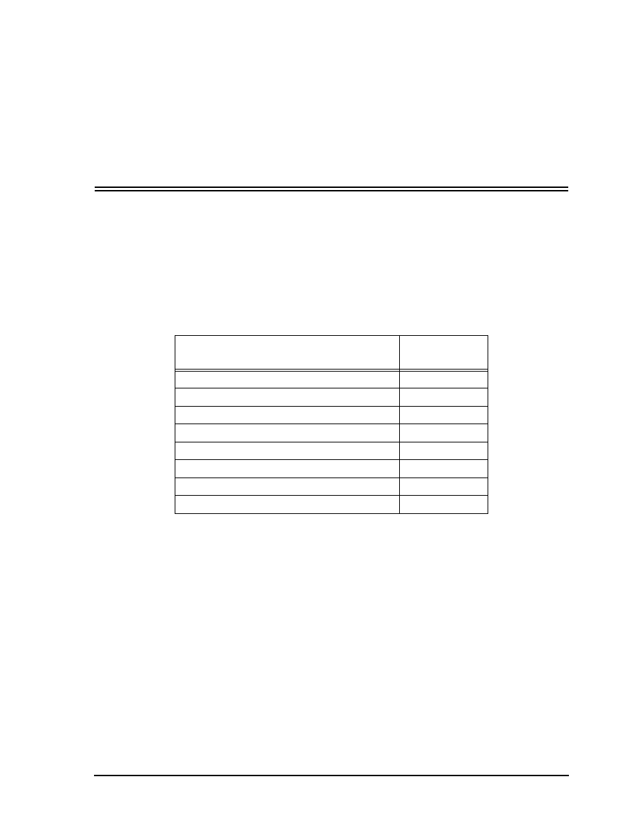
Table 1
Additional Documentation
Document Name
Description
Order Number
DSP96002 User's Manual
Detailed description of the DSP96002 core
processor and peripherals
DSP96002UM/AD
DSP96002 Data Sheet
Electrical and timing specifications, and pin and
package descriptions
DSP96002/D
F
r
e
e
s
c
a
l
e
S
e
m
i
c
o
n
d
u
c
t
o
r
,
I
Freescale Semiconductor, Inc.
For More Information On This Product,
Go to: www.freescale.com
n
c
.
.
.
MOTOROLA
DSP96002/D, Rev. 2
1-1
SECTION 1
SIGNAL/CONNECTION DESCRIPTIONS
SIGNAL GROUPINGS
The input and output signals of the DSP96002 are organized into eight functional
groups, as shown in
Table 1-1
and as illustrated in
Figure 1-1
.
Figure 1-1
is a diagram of DSP96002 signals by functional group.
Table 1-1
DSP96002 Functional Signal Groupings
Functional Group
Detailed
Description
Power (V
CCN
and V
CCQ
)
Table 1-2
Ground (GND
N
and GND
Q
)
Table 1-3
Clock (CLK)
Table 1-4
Interrupt and Mode Control
Table 1-5
Port A (Address, Data, and Control)
Table 1-6
Port B (Address, Data, and Control)
Table 1-6
Timer/Event Counters
Table 1-7
OnCE Port
Table 1-8
F
r
e
e
s
c
a
l
e
S
e
m
i
c
o
n
d
u
c
t
o
r
,
I
Freescale Semiconductor, Inc.
For More Information On This Product,
Go to: www.freescale.com
n
c
.
.
.