 | ÐлекÑÑоннÑй компоненÑ: EB212 | СкаÑаÑÑ:  PDF PDF  ZIP ZIP |
Äîêóìåíòàöèÿ è îïèñàíèÿ www.docs.chipfind.ru
EB212
Using Data Sheet Impedances
for RF LDMOS Devices
Prepared by: Darin Wagner
Motorola Semiconductor Products Sector
INTRODUCTION
This document explains the format used by Motorola for
presenting LDMOS impedance information for both
single -ended and push-pull devices on RF Power data
sheets. The purpose of this document is to clarify the use of
this information in the initial design of input and output
matching networks for these devices.
Multiple methods are available for impedance extraction.
The scope of this document does not cover detailed extraction
methods; however, a possible extraction method is explained
here. Whichever method is used, the main concern to be
addressed is the need to de-embed the extracted data back
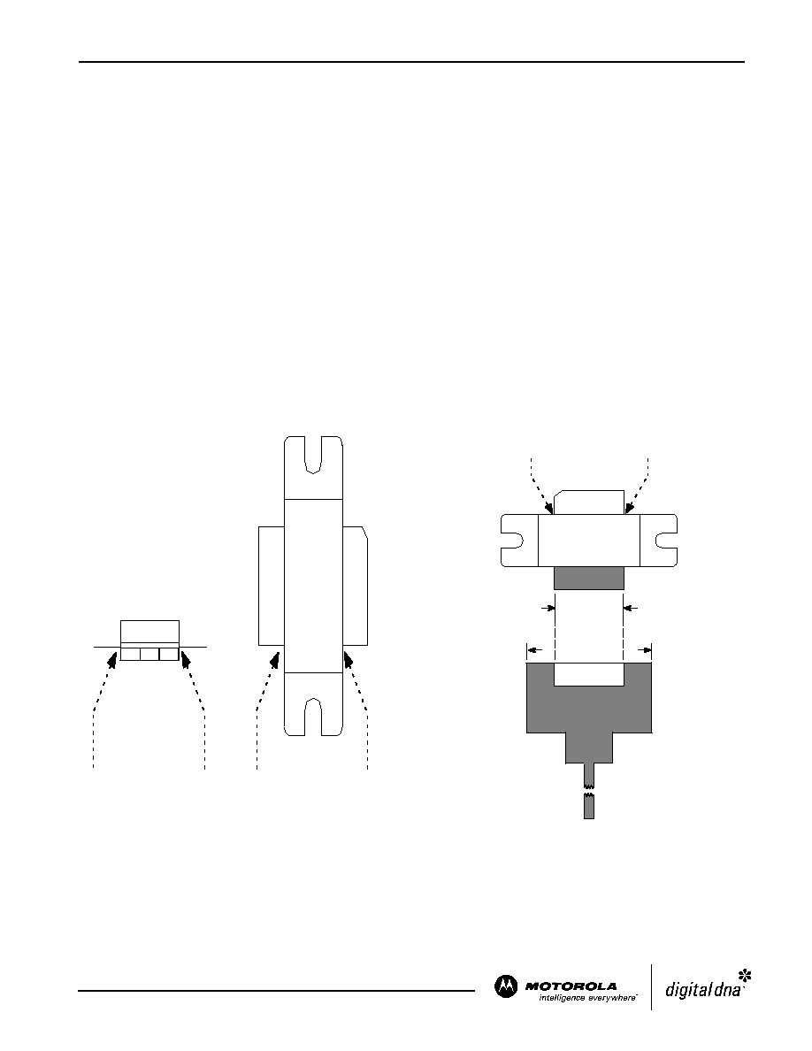
to the reference plane of the device as shown in Figure 1.
As a byproduct of the impedance extraction methodology,
a zero length width step simulation block should be used
during simulation The MSTEP block for Agilent Advanced
Design System (ADS) users shows the difference between
the reference plane width and the copper lead pad width.
Figure 2 illustrates that the copper lead pad width (Dimension
"b") is larger than the reference plane width (Dimension "a").
For more information on this topic, the reference provided
at the end of this document is a rigorous but accurate method
for impedance measurements:
ÎÎÎÎ
DUT
Reference Planes
DUT
Reference Planes
b
a
MRF
XXXXX
DUT Reference Plane
Figure 1. Location of Reference Planes on a Package
Figure 2. Illustration of the Instantaneous
Impedance Change and Need for MSTEP Blocks
b
Order this document
by EB212/D
MOTOROLA
SEMICONDUCTOR ENGINEERING BULLETIN
Motorola, Inc. 2004
REV 0
F
r
e
e
s
c
a
l
e
S
e
m
i
c
o
n
d
u
c
t
o
r
,
I
Freescale Semiconductor, Inc.
For More Information On This Product,
Go to: www.freescale.com
n
c
.
.
.
EB212
2
MOTOROLA SEMICONDUCTOR APPLICATION INFORMATION
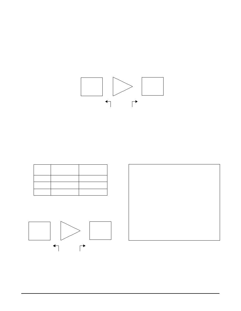
SINGLEENDED DEVICES
The data sheet impedance format for single-ended devices
is illustrated in Figure 3. The impedance data is taken by
tuning the fixture for optimum* performance and then
measuring the impedance at the device reference plane.
Figure 4 shows the format for in-band frequency-depend -
ent impedances that should be presented to the device for
optimal performance. This measured data can be turned into
an S1P file as shown in Figure 5.
Note: The imaginary portion of the measured impedance
data has been conjugated from the data shown in Figure 4.
The impedances are to be conjugated from the data sheet
to account for rotation of reference frames. This means that
when data is first acquired, the measured data represents
impedances as seen by looking into the input side RF launch
point. However, the data needs to be presented as looking into
the part for S
1,1
optimization. This is the reason for the
redirection of the arrows as well as the conjugation of the
measured impedance data.
*
An optimum tuned fixture will be tuned for overall peak performance considering all major parameters:
input return loss (IRL), efficiency, P
1dB
, linearity, maximum output power (P
out
) and bandwidth.
Z
source
= Test circuit impedance as measured from
gate to ground.
Z
load
= Test circuit impedance as measured
from drain to ground.
Z source
Z load
Input
Matching
Network
Device
Under Test
Output
Matching
Network
Figure 3. Data Sheet Impedance Format for
SingleEnded Devices
Figure 4. Optimal Impedances for an MRF19125
Test Fixture
f
MHz
Z
source
Z
load
1930
1960
1990
1.43 - j5.01
1.56 - j4.93
1.51 - j4.88
0.75 - j0.93
0.71 - j0.89
0.68 - j1.02
Z
source
= Test circuit impedance as measured from
gate to ground.
Z
load
= Test circuit impedance as measured
from drain to ground.
Z source
Z load
Input
Matching
Network
Device
Under Test
Output
Matching
Network
!
S11 (input) file
!
Circuit
: MRF19125
!
Author
: John Q. Designer
!
Date
: 01/01/2003
!
File
: mrf19125_zin.s1p
!
!
File Format:
#
MHz
Z
RE
IM
!
!
1930
1.43
5.01
1960
1.51
4.88
1990
1.56
4.93
!
!
End of File
Figure 5. S1P File of Impedances to Be Used
at Input Block
F
r
e
e
s
c
a
l
e
S
e
m
i
c
o
n
d
u
c
t
o
r
,
I
Freescale Semiconductor, Inc.
For More Information On This Product,
Go to: www.freescale.com
n
c
.
.
.
EB212
3
MOTOROLA SEMICONDUCTOR APPLICATION INFORMATION
Matching
Network
S
11
< -30 dB
50
Z (Device)
Z*
Data Sheet
Figure 6. Generalized Schematic Used to Optimize Matching Network
MSTEP
a
b
Note: When using the impedances presented in this
engineering bulletin, the designer should assume that the
impedances are based on a 50 system, even though some
Smith charts may use normalized impedances of different
values for display purposes only.
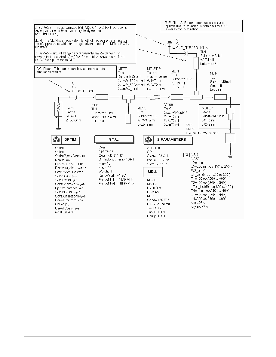
The block diagram in Figure 6 has a generic matching circuit
that will be used for an optimization of the first-pass matching
network.
The MRF19125 impedance data from Figure 5 is used to
illustrate this as a practical example for developing a
first -pass matching network as shown in Figure 8. A few key
details are as follows:
· The S1P file was used as a two-port (reference is the
grounded port) device and its file name formatting.
· The DC_Block and BYPASS capacitors are shown with
generic values.
· The MLIN, ideally, should have an electrical length of / 4
from the DC feed - DUT junction.
· The simplified C_BYPASS capacitor elements placement
should be as close as possible to the length of the MLIN.
Note: A sample matching network is shown, but this may be
changed to a topology of any configuration.
The MSTEP block, discussed earlier, must be placed
between the device and the first matching element MLIN (see
Figures 6, 8, 10 and 11 for details on placement). This block
is important because it is used to determine the difference
between the reference plane width and the copper lead pad
width. If these values are not the same, there will be an
impedance discontinuity. The MSTEP is specified by its width
values ("a" and "b"). The value for Dimension "a" is found in the
package dimension section of the data sheet. Dimension "b"
is the width of the copper pad on the PCB that the lead is to
be seated on.
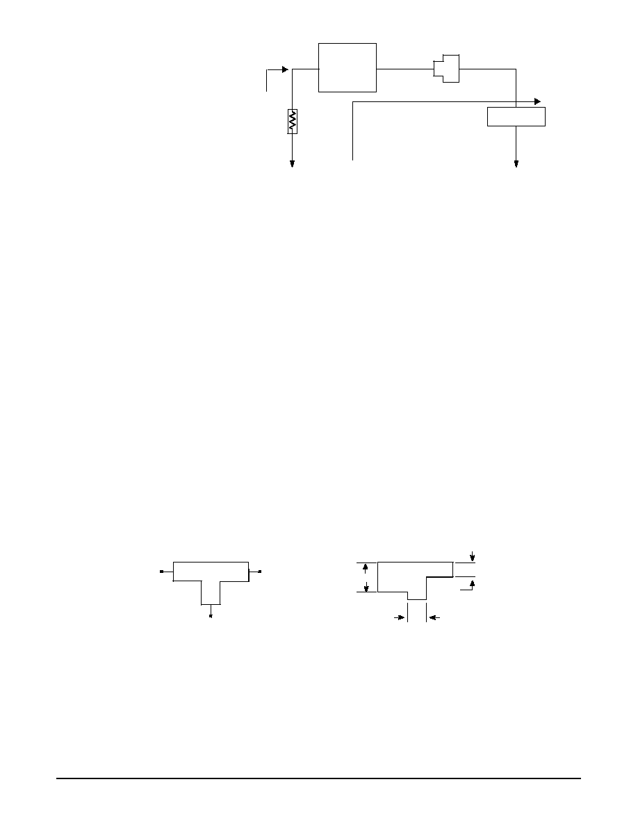
The MTEE, another ADS block, is used to connect the bias
feed (see Figure 7). The MTEE has design rules that are
violated in typically optimized fixture layouts. A simple nodal
connection has been found to be sufficient to simulate this
accurately. However, it is recommended to use the MTEE
within its usage constraints if at all possible.
So far the impedance data has been acquired, conjugated
and reinserted into an *.s1p file. The next step is to run an
S-parameter optimization simulation using the SP1 block, as
illustrated in Figure 8. Then the matching network should be
tuned to an S
1,1
of at least -30 dB (or as low as possible),
resulting in a first-pass input match circuit. This process
should be repeated using the output impedances to generate
the output match. Finally, the matching networks are ready for
realization on a printed circuit board.
W1 = conductor width at pin 1, in specified units
W2 = conductor width at pin 2, in specified units
W3 = conductor width at pin 3, in specified units
0.05 x H
W1 20 x H
0.05 x H
W2 20 x H
0.05 x H
W3 20 x H
r
20
MTEE Design Rules
Figure 7. Design Constraints for the MTEE Block
Symbol
Illustration
1
3
2
3
2
1
W1
W3
W2
W (largest) / W (smallest)
5
W (largest) and W (smallest) are the largest and smallest
widths among W1, W2 and W3
f (GHz) x H (mm)
0.4 x Z
o
Z
o
is the characteristic impedance
F
r
e
e
s
c
a
l
e
S
e
m
i
c
o
n
d
u
c
t
o
r
,
I
Freescale Semiconductor, Inc.
For More Information On This Product,
Go to: www.freescale.com
n
c
.
.
.
EB212
4
MOTOROLA SEMICONDUCTOR APPLICATION INFORMATION
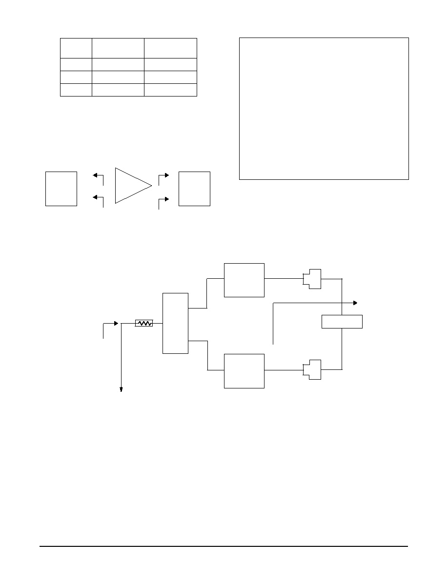
Figure 8. Optimization Layout for Input Matching Network of the MRF19125
F
r
e
e
s
c
a
l
e
S
e
m
i
c
o
n
d
u
c
t
o
r
,
I
Freescale Semiconductor, Inc.
For More Information On This Product,
Go to: www.freescale.com
n
c
.
.
.
EB212
5
MOTOROLA SEMICONDUCTOR APPLICATION INFORMATION
f
MHz
Z
source
Z
load
2110
2140
2170
2.65 + j1.52
2.64 + j2.04
2.71 + j1.80
2.45 + j2.08
2.39 + j2.51
2.16 + j3.14
Z
source
= Test circuit impedance as measured from
gate to gate, balanced configuration.
Z
load
= Test circuit impedance as measured
from drain to drain, balanced configuration.
Z source
Z load
Input
Matching
Network
Device
Under
Test
Output
Matching
Network
-
-
+
+
Figure 9. Data Sheet Representation of the
MRF21180 Push-Pull Device
!
S11 (input) file
!
Circuit
: MRF21180
!
Author
: John Q. Designer
!
Date
: 01/01/2003
!
File
: mrf21180_zin.s1p
!
!
File Format:
#
MHz
Z
RE IM
!
!
2110
2.45
-2.08
2140
2.39
-2.51
2170
2.16
-3.14
!
!
End of File
Figure 10. S2P File of Impedances to Be Used
at Input Block
S
11
< -30 dB
50
Z (Device)
Z*
Data Sheet
Balun
n:1
Matching
Network
Matching
Network
+
-
MSTEP
a
b
MSTEP
a
b
Figure 11. Generalized Schematic Used to Optimize Matching Network
PUSHPULL DEVICES
The methods for taking impedance data on fixtures for
push -pull parts are similar to those for single-ended parts.
The representation for push-pull device impedances is shown
in Figure 9.
Push-pull device impedance data should be presented in
a data storage device, such as the one shown in Figure 10.
Note: The imaginary portion of the measured impedance
data has been conjugated from the data shown in Figure 9, the
same process as for the single-ended devices.
The methods for optimizing first-pass input and output side
matching networks for pushpull devices are the same as for
single -ended devices.
The circuit shown in Figure 11 is a generic matching circuit
that is used for an optimization of a first-pass input side
matching network. The balun shown in Figure 11 is an
idealized three-port device with a generic input/output
impedance ratio of n:1.
F
r
e
e
s
c
a
l
e
S
e
m
i
c
o
n
d
u
c
t
o
r
,
I
Freescale Semiconductor, Inc.
For More Information On This Product,
Go to: www.freescale.com
n
c
.
.
.