MOTOROLA
SEMICONDUCTOR TECHNICAL DATA
This document contains certain information on a new product.
Specifications and information herein are subject to change without notice.
© Motorola, Inc. 2002
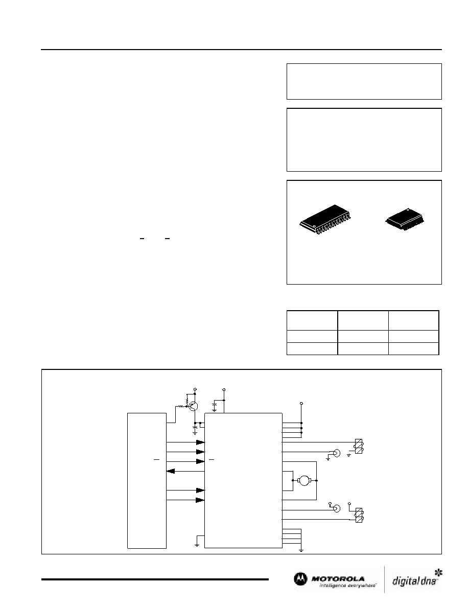
33880 Simplified Application Schematic
Document order number: MC33880/D
Rev 1, 09/2002
33880
Advance Information
Configurable Octal Serial Switch
with Serial Peripheral Interface I/O
The 33880 device is an eight output hardware configurable high side/low
side switch with 8-bit serial input control. Two of the outputs may be controlled
directly via microprocessor for PWM applications. The 33880 incorporates
SMARTMOS
TM
technology, with CMOS logic, bipolar/MOS analog circuitry,
and DMOS power MOSFETs. The 33880 controls various inductive or
incandescent loads by directly interfacing with a micro controller. The circuit's
innovative monitoring and protection features include: very low standby
currents; cascade fault reporting; internal +40 V clamp voltage for low side
configuration; -20 V high side configuration; output specific diagnostics; and
independent shutdown of output.
Features
∑ Designed to operate 5.5 V < V
PWR
< 24.5 V
∑ 8-Bit SPI for Control and Fault Reporting, 3.3 V/5.0 V Compatible
∑ Outputs are current limited (0.8 A to 2 A) to Drive Incandescent Lamps
∑ Output voltage Clamp, +45 V (low side) and -20 V (high side) During
Inductive Switching
∑ Internal Reverse Battery Protection on V
PWR
∑ Loss of Ground or Supply Will Not Energize Loads or Damage IC
∑ Maximum 5 µA I
PWR
Standby Current at 13.0 V V
PWR
∑ R
DS(ON)
of 0.55
at 25
∞
C Typical
∑ Short Circuit Detect and Current Limit with Automatic Retry
∑ Independent Over Temperature Protection
Package Options
CONFIGURABLE OCTAL SERIAL
SWITCH WITH SERIAL
PERIPHERAL INTERFACE
32-Lead Fine
Pitch SOIC
CASE 1324
28-Lead SOIC
Case751F
ORDERING INFORMATION
Device
Temperature
Range (T
A
)
Package
PC33880DW
-40
∞
C
to 125
∞
C
28 Ld SOIC
PC33880DWB
-40
∞
C
to 125
∞
C
32 Ld SOIC
D1
D2
D3
D4
M
S1
S2
S3
S4
V
BAT
V
BAT
D5
D6
D7
D8
S5
S6
S7
S8
V
BAT
DI
DO
SCLK
CS
33880
+5.0V
V
DD
EN
V
PWR
V
PWR
MCU
MOSI
SCLK
CS
MISO
IN5
IN6
PWM1
PWM2
H-Bridge Configuration
High Side Drive
Low Side Drive
A0
GND
33880
MOTOROLA ANALOG INTEGRATED CIRCUIT DEVICE DATA
2
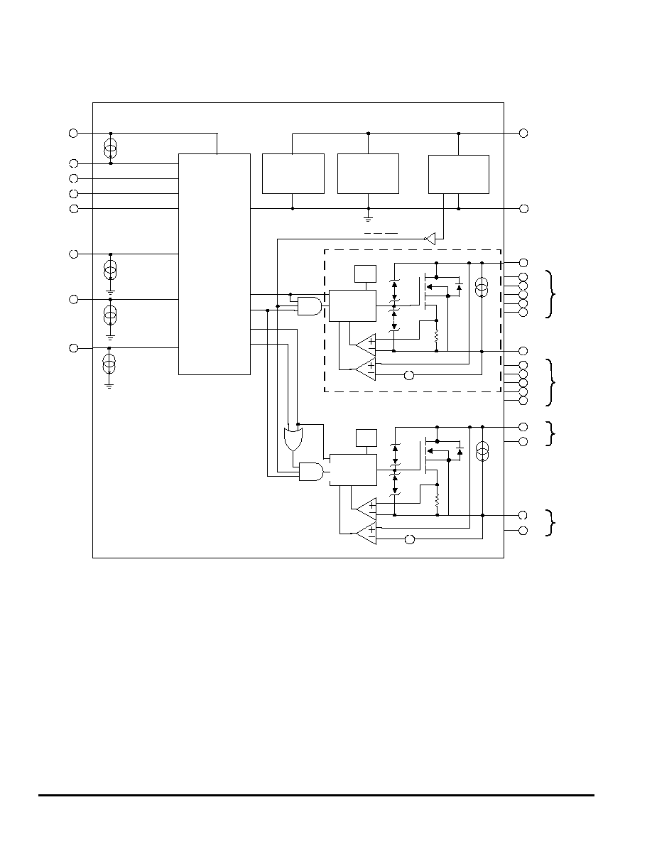
Figure 1. 33880 Simplified Block Diagram
SPI Bit 4
IN5
SPI Bit 0
OV, POR, SLEEP
~50uA
~50uA
T- lim
Gate
Drive
Control
Current
Limit
Open
Load
Detect
Current
_
+
~1.5V Open/Short
Threshold
Open/Short
Comparator
~650uA
CS
__
SCLK
DI
DO
~50uA
EN
V
DD
~50uA
IN5
IN6
Internal
Bias
Charge
Pump
Over Voltage
Shutdown/POR
SPI & Interface
Logic
Sleep State
T- lim
Gate
Drive
Control
Current
Limit
Open
Load
Detect
Current
_
+
~1.5V Open/Short
Threshold
Open/Short
Comparator
~650uA
enable
VPWR
GND
D1
D2
D3
D4
D7
D8
Typical of all 8 output drivers
S1
Drain
Outputs
S2
S3
S4
S7
S8
Source
Outputs
D5
D6
S5
S6
Drain
Outputs
Source
Outputs
MOTOROLA ANALOG INTEGRATED CIRCUIT DEVICE DATA
33880
3
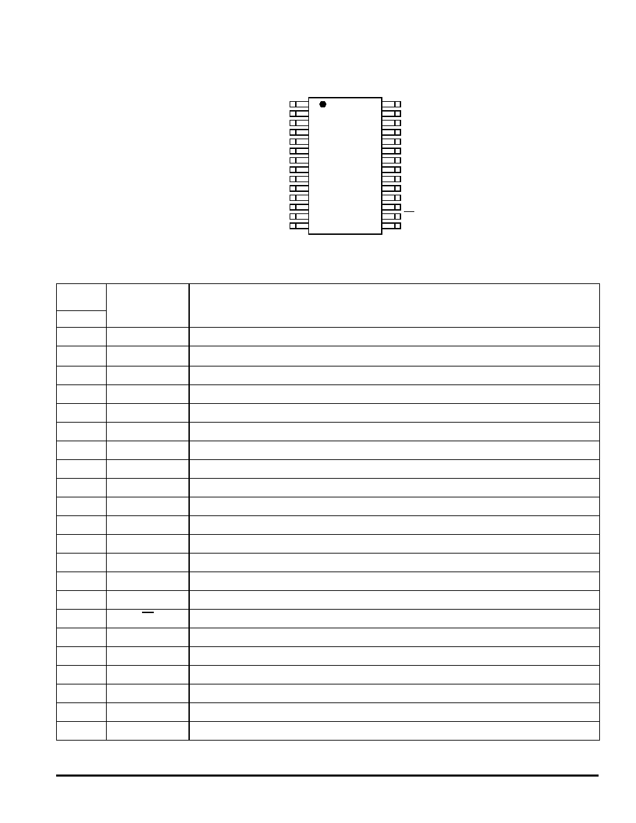
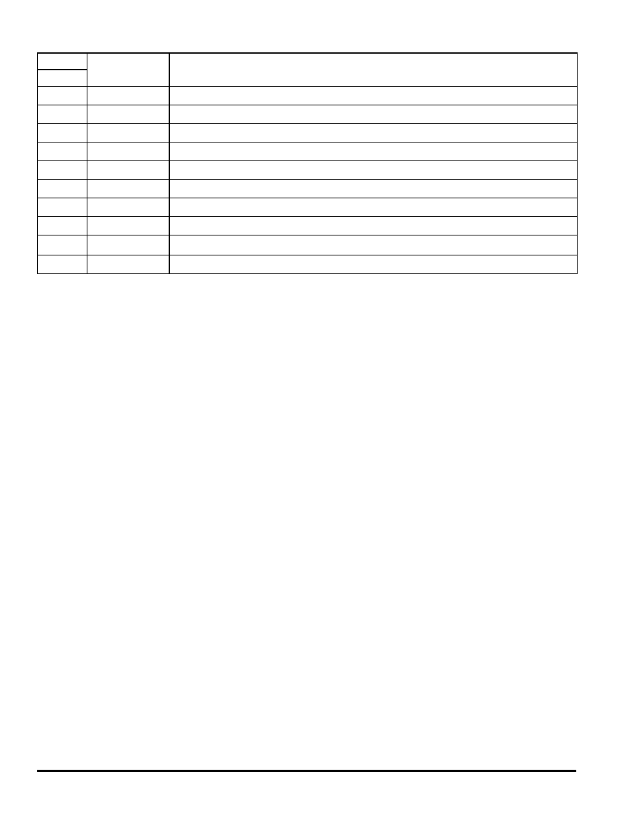
PIN FUNCTION DESCRIPTON 28 SOIC
28-Lead
SOIC
PIN NAME
DESCRIPTION
PIN
1
GND
Digital ground.
2
V
DD
Logic supply voltage. Logic supply must be switched off for low current mode (V
DD
below 3.9 V).
3
S8
Output eight MOSFET source pin.
4
S8
Output eight MOSFET source pin.
5
D8
Output eight MOSFET drain pin.
6
S2
Output two MOSFET source pin.
7
D2
Output two MOSFET drain pin.
8
S1
Output one MOSFET source pin.
9
D1
Output one MOSFET drain pin.
10
D6
Output six MOSFET drain pin.
11
S6
Output six MOSFET source pin.
12
IN6
PWM direct control input pin for output 6. IN6 is "OR" with SPI bit.
13
EN
Enable input. Allows control of outputs. Active high.
14
SCLK
SPI control clock input pin.
15
DI
SPI control data input pin from MCU to the 33880. Logic 1 activates output.
16
CS
SPI control chip select input pin from MCU to the 33880. Logic 0 allows data to be transferred in.
17
IN5
PWM direct control input pin for output 5. IN5 is "OR" with SPI bit.
18
S5
Output five MOSFET source pin.
19
D5
Output five MOSFET drain pin.
20
D3
Output three MOSFET drain pin.
21
S3
Output three MOSFET source pin.
22
D4
Output four MOSFET drain pin.
1
2
3
4
5
6
7
8
9
10
11
12
13
14
15
28
27
26
25
24
23
22
21
20
19
18
17
16
28 Lead SOIC
DO
VPWR
S7
S7
D7
S4
D4
S3
D3
D5
S5
IN5
CS
DI
GND
VDD
S8
S8
D8
S2
D2
S1
D1
D6
S6
IN6
EN
SCLK
33880
MOTOROLA ANALOG INTEGRATED CIRCUIT DEVICE DATA
4
23
S4
Output four MOSFET source pin.
24
D7
Output seven MOSFET drain pin.
25
S7
Output seven MOSFET source pin.
26
S7
Output seven MOSFET source pin.
27
V
PWR
Power supply pin to the 33880. V
PWR
has internal reverse battery protection.
28
DO
SPI control data output pin from the 33880 to the MCU. DO= 0 no fault, DO= 1 specific output has fault.
PIN FUNCTION DESCRIPTON 28 SOIC
28-Lead
SOIC
PIN NAME
DESCRIPTION
PIN

MOTOROLA ANALOG INTEGRATED CIRCUIT DEVICE DATA
33880
5
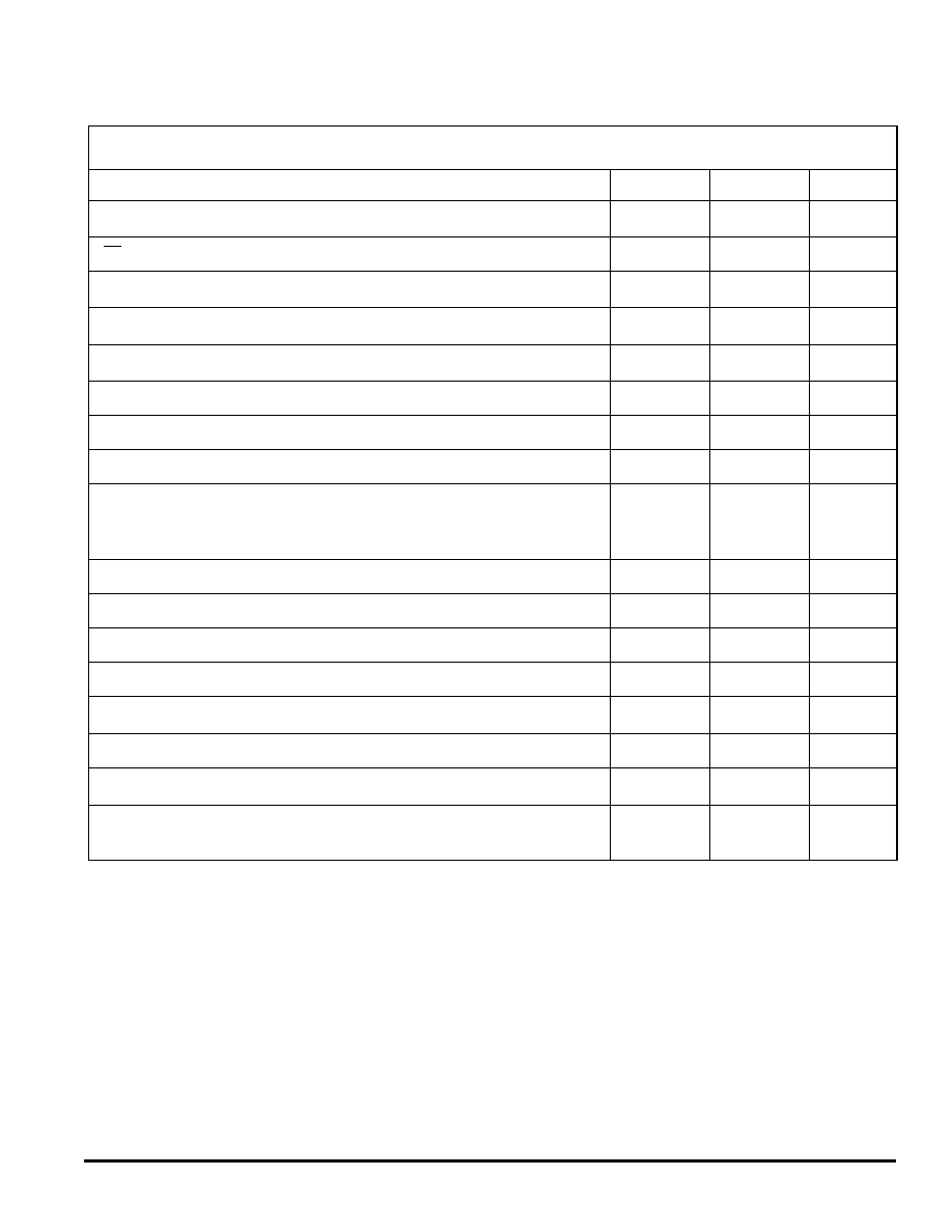
PIN FUNCTION DESCRIPTON 32 SOIC
SOIC-32
PIN NAME
DESCRIPTION
PIN
1
GND
Digital ground.
2
V
DD
Logic supply voltage. Logic supply must be switched off for low current mode (V
DD
below 3.9 V).
3
S8
Output eight MOSFET source pin.
4
S8
Output eight MOSFET source pin.
5
D8
Output eight MOSFETdrain pin.
6
S2
Output two MOSFET source pin.
7
D2
Output two MOSFET drain pin.
8
GND
Thermal enhanced ground pin.
9
GND
Thermal enhanced ground pin.
10
S1
Output one MOSFET source pin.
11
D1
Output one MOSFET drain pin.
12
D6
Output six MOSFETdrain pin.
13
S6
Output six MOSFET source pin.
14
IN6
PWM direct control input pin for output 6. IN6 is "AND" with SPI bit.
15
EN
Enable input. Allows control of outputs. Active high.
16
SCLK
SPI control clock input pin.
17
DI
SPI control data input pin from MCU to the 33880. Logic 1 activates output.
18
CS
SPI control chip select input pin from MCU to the 33880. Logic 0 allows data to be transferred in.
19
IN5
PWM direct control input pin for output 5. IN5 is "AND" with SPI bit.
20
S5
Output five MOSFET source pin.
21
D5
Output five MOSFET drain pin.
22
D3
Output three MOSFET drain pin.
1
2
3
4
5
6
7
8
9
10
11
12
13
14
15
16
17
32
31
30
29
28
27
26
25
24
23
22
21
20
19
18
32 Lead SOIC
DO
VPWR
S7
S7
D7
S4
D4
GND
GND
S3
D3
D5
S5
IN5
CS
DI
GND
VDD
S8
S8
D8
S2
D2
GND
GND
S1
D1
D6
S6
IN6
EN
SCLK
33880
MOTOROLA ANALOG INTEGRATED CIRCUIT DEVICE DATA
6
23
S3
Output three MOSFET source pin.
24
GND
Thermal enhanced ground pin.
25
GND
Thermal enhanced ground pin.
26
D4
Output four MOSFET drain pin.
27
S4
Output four MOSFET source pin.
28
D7
Output seven MOSFET drain pin.
29
S7
Output seven MOSFET source pin.
30
S7
Output seven MOSFET source pin.
31
V
PWR
Power supply pin to the 33880. V
PWR
has internal reverse battery protection.
32
DO
SPI control data output pin from the 33880 to the MCU. DO= 0 no fault, DO= 1 specific output has fault.
PIN FUNCTION DESCRIPTON 32 SOIC
SOIC-32
PIN NAME
DESCRIPTION
PIN
MOTOROLA ANALOG INTEGRATED CIRCUIT DEVICE DATA
33880
7
MAXIMUM RATINGS
All voltages are with respect to ground unless otherwise noted.
Rating
Symbol
Value
Unit
V
DD
Supply Voltage (Note1)
V
DD
-0.3 to 7.0
V
DC
CS, DI, DO, SCLK, IN5, IN6, and EN (Note1)
--
-0.3 to 7.0
V
DC
V
PWR
Supply Voltage (Note1)
V
PWR
-16 to 50
V
DC
Drain 1 - 8 (5.0 mA
I
OUT
0.3 A) (Note2)
--
-18 to 40
V
DC
Source 1 - 8 (5.0 mA
I
OUT
0.3 A) (Note3)
--
-28 to 40
V
DC
Output Voltage Clamp Low Side Drive (Note4)
V
OC
40 to 55
V
DC
Output Voltage Clamp High Side Drive (Note4)
V
OC
-15 to -25
V
DC
Output Clamp Energy (Note5)
E
CLAMP
50
mJ
ESD Voltage
Human Body Model (Note6)
Machine Model (Note7)
V
ESD1
V
ESD2
2000
200
V
V
Storage Temperature
T
STG
-55
∞
to +150
∞
∞
C
Operating Case Temperature
T
C
-40
∞
to +125
∞
∞
C
Operating Junction Temperature
T
J
-40
∞
to +150
∞
∞
C
Maximum Junction Temperature
--
-40
∞
to +150
∞
∞
C
Power Dissipation 28-SOIC, Case 751F (T
a
= 25
∞
C) (Note8)
P
D
1.3
W
Thermal Resistance, Junction-to-Ambient Plastic Package 28 SOIC, Case 751F
R
JA
94
∞
C/W
Power Dissipation 32-SOIC, Case 1324 (T
a
= 25
∞
C) (Note8)
PD
1.7
W
Thermal Resistance, Junction-to-Ambient, Plastic Package 32SOIC, Case 1324,
Thermal Resistance Junction to thermal ground leads.
R
JA
R
JL
70
18
∞
C/W
Notes:
1.
Exceeding these limits may cause malfunction or permanent damage to the device.
2.
Configured as Low Side Driver with 300 mA load as current limit.
3.
Configured as High Side Driver with 300 mA load as current limit.
4.
With outputs OFF and 10 mA of test current for low side drive, 30 mA test current for high side drive.
5.
Maximum output clamp energy capability at 150
∞
C junction temperature using single non-repetitive pulse method.
6.
ESD1 testing is performed in accordance with the Human Body Model (C
Zap
= 100 pF, R
Zap
= 1500
).
7.
ESD2 testing is performed in accordance with the Machine Model (C
Zap
= 200 pF, R
Zap
= 0
).
8.
Maximum power dissipation with no heat sink used.
33880
MOTOROLA ANALOG INTEGRATED CIRCUIT DEVICE DATA
8
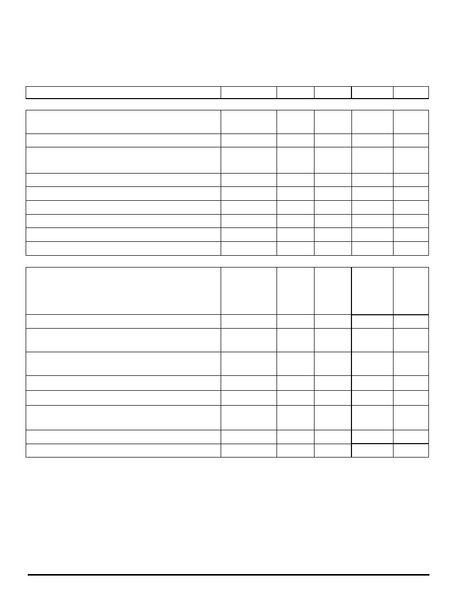
STATIC ELECTRICAL CHARACTERISTICS
Characteristics noted under conditions of 4.75 V
V
DD
5.25 V, 9.0 V
V
PWR
16 V, -40
∞
C
T
C
125
∞
C, unless otherwise noted.
Typical values, where applicable, reflect the parameter's approximate average value with V
PWR
= 13 V, T
A
= 25
∞
C
Characteristic
Symbol
Min
Typ
Max
Unit
Power Input
Supply Voltage Range
Fully Operational
V
PWR(fo)
5.5
--
24.5
V
Supply Current
I
PWR(on)
--
8.0
14
mA
Sleep State Supply Current (V
DD
and EN
0.5 V)
V
PWR
= 16.0 V
I
PWR(ss)
--
--
2.0
--
5.25
25
µA
Over Voltage Shutdown
V
OV
25
27
30
V
Over Voltage Shutdown Hysteresis
V
OV(hys)
0.2
0.8
2.5
V
Logic Supply Voltage
V
DD
4.75
--
5.25
V
Logic Supply Current
I
DD
0.5
2.6
4.0
mA
Logic Supply Under Voltage Lockout Threshold
V
DD(unvol)
3.9
4.3
4.6
V
Logic Supply Under Voltage Hysteresis
V
DD(unvol-hys)
100
150
300
mV
Power Output
Drain-to-Source ON Resistance
(I
OUT
= 0.250 A, T
J
= 125
∞
C)
(I
OUT
= 0.250 A, T
J
= 25
∞
C)
(I
OUT
= 0.250 A, T
J
= -40
∞
C)
R
DS (on)
--
--
--
0.75
0.55
0.45
1.1
0.85
0.80
Output Self Limiting Current High Side and Low Side Configurations
I
OUT(LIM)
0.8
1.4
2.0
A
Output Fault Detect Threshold (Note9)(Note10)
Outputs Programmed Off
V
OUTth(F)
1.0
--
3.0
V
Output Off Open Load Detect Current (Note9)
Outputs Programmed OFF
I
OCO
0.30
0.55
0.9
mA
Output Clamp Voltage Low Side Drive (I
D
= 10 mA)
V
OC(LSD)
40
45
55
V
Output Clamp Voltage High Side Drive (I
S
= -30 mA)
V
OC(HSD)
-15
-20
-25
V
Output Leakage Current High Side and Low Side Configuration
(V
DD
= 0 V, V
DS
= 16 V)
I
OUT(LKG)
--
--
7.0
µA
Over Temperature Shutdown (Note10)
T
LIM
155
--
185
∞
C
Over Temperature Shutdown Hysteresis (Note10)
T
LIM(HYST)
5.0
10
15
∞
C
Notes:
9.
Output Fault Detect Thresholds with outputs programmed OFF. Output fault detect threshold are the same for output open and shorts.
10.
This parameter is guaranteed by design, but not production tested.
MOTOROLA ANALOG INTEGRATED CIRCUIT DEVICE DATA
33880
9
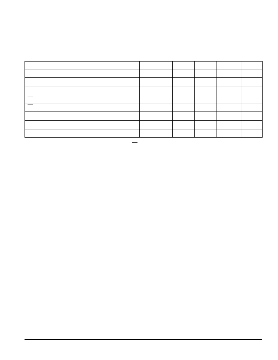
STATIC ELECTRICAL CHARACTERISTICS
Characteristics noted under conditions of 4.75 V
V
DD
5.25 V, 9.0 V
V
PWR
16 V, -40
∞
C
T
C
125
∞
C, unless otherwise noted.
Typical values, where applicable, reflect the parameter's approximate average value with V
PWR
= 13 V, T
A
= 25
∞
C
Digital Interface
Input Logic Voltage Thresholds (Note11)
V
INLOGIC
0.8
--
2.2
V
IN5, IN6, EN Input Logic Current (IN5,IN6,EN = 0 V)
I
IIN5,IN6,EN
-10
--
10
µA
IN5, IN6, EN Pull-Down Current (0.8 V to V
DD
)
I
IIN5,IN6,EN
30
45
100
µA
SCLK, DI, Tri-state DO Input (0 V to V
DD
)
I
SCK,SI,TriSO
-10
--
10
µA
CS Input Current (CS = V
DD
)
I
ICS
-10
--
10
µA
CS Pull-Up Current (CS = 0 V)
I
ICS
-30
--
-100
µA
DO High State Output Voltage (I
DO-HIGH
= -200 µA)
V
DOHIGH
V
DD
- 0.8
--
V
DD
V
DO Low State Output Voltage (I
DO-HIGH
= 1.6 mA)
V
DOLOW
--
--
0.4
V
Input Capacitance on SCLK, DI, Tri-state DO, IN5, IN6, EN (Note12)
C
IN
--
--
20
pF
Notes:
11.
Upper and lower logic threshold voltage levels apply to DI, CS, SCLK, IN5, IN6, EN.
12.
This parameter is guaranteed by design, but not production tested.

33880
MOTOROLA ANALOG INTEGRATED CIRCUIT DEVICE DATA
10
DYNAMIC ELECTRICAL CHARACTERISTICS
Characteristics noted under conditions of 4.75 V
V
DD
5.25 V, 9.0 V
V
PWR
16 V, -40
∞
C
T
C
125
∞
C, unless otherwise
noted. Typical values, where applicable, reflect the parameter's approximate average value with V
PWR
= 13 V, T
A
= 25
∞
C
Characteristic
Symbol
Min
Typ
Max
Units
Power Output Timing
Output Rise Time Low Side Configuration (RL = 620
) (Note13)
t
R
0.1
0.5
1.0
V/µs
Output Fall Time Low Side Configuration (RL = 620
) (Note13)
t
F
0.1
0.5
1.0
V/µs
Output Rise Time High Side Configuration (RL = 620
) (Note13)
t
R
0.1
0.3
1.0
V/µs
Output Fall Time High Side Configuration (RL = 620
) (Note13)
t
F
0.1
0.3
1.0
V/µs
Output Turn ON Delay Time, High Side and Low Side Configuration
(Note14)
t
DLY(on)
1.0
15
50
µs
Output Turn OFF Delay Time, High Side and Low Side Configuration
(Note14)
t
DLY(off)
1.0
30
100
µs
Output Fault Delay Time (Note15)
t
FAULT
100
--
300
µs
Notes::
13.
Output Rise and Fall time respectively measured across a 620
resistive load at 10 to 90 percent and 90 to 10percent voltage points.
14.
Output turn ON and OFF delay time measured from 50 percent rising edge of CS to 90 and 10 percent of initial voltage.
15.
Duration of fault before fault bit is set. Duration between access times must be greater than 300 µS to read faults.

MOTOROLA ANALOG INTEGRATED CIRCUIT DEVICE DATA
33880
11
Figure 2. SPI Timing Diagram
Digital Interface Timing
Recommended Frequency of SPI Operation
--
4.0
6.0
MHz
Required Low State Duration on V
DD
for Reset (V
DD
0.2 V) (Note16)
t
RESET
--
4.0
10
µs
Falling Edge of CS to Rising Edge of SCLK (Required Setup Time)
t
LEAD
100
--
--
ns
Falling Edge of SCLK to Rising Edge of CS (Required Setup Time)
t
LAG
50
--
--
ns
DI to Falling Edge of SCLK (Required Setup Time)
t
DI(su)
16
--
--
ns
Falling Edge of SCLK to DI (Required Hold Time)
t
DI(HOLD
)
20
--
--
ns
DI, CS, SCLK Signal Rise Time (Note17)
t
r(DI)
--
5
--
ns
DI, CS, SCLK Signal Fall Time (Note17)
t
f(DI)
--
5
--
ns
Time from Falling Edge of CS to DO Low Impedance (Note18)
t
DO(EN)
--
--
55
ns
Time from Rising Edge of CS to DO High Impedance (Note19)
t
DO(DIS)
--
--
55
ns
Time from Rising Edge of SCLK to DO Data Valid (Note20)
t
VALID
--
25
55
ns
Notes:
16.
This parameter is guaranteed by design, but not production tested.
17.
Rise and Fall time of incoming DI, CS, and SCLK signals suggested for design consideration to prevent the occurrence of double pulsing.
18.
Time required for output status data to be available for use at DO pin.
19.
Time required for output status data to be terminated at DO pin
20.
Time required to obtain valid data out from DO following the rise of SCLK.
DYNAMIC ELECTRICAL CHARACTERISTICS
Characteristics noted under conditions of 4.75 V
V
DD
5.25 V, 9.0 V
V
PWR
16 V, -40
∞
C
T
C
125
∞
C, unless otherwise
noted. Typical values, where applicable, reflect the parameter's approximate average value with V
PWR
= 13 V, T
A
= 25
∞
C
Characteristic
Symbol
Min
Typ
Max
Units
t
DO(dis)
0.7 V
DD
0.2 V
DD
0.2 V
DD
0.7 V
DD
0.2 V
DD
t
lead
t
DO(en)
t
DI(su)
t
DI(hold)
t
valid
t
lag
CS
SCLK
DI
DO
MSB in
MSB out
LSB out
0.7 V
DD
0.2 V
DD
33880
MOTOROLA ANALOG INTEGRATED CIRCUIT DEVICE DATA
12
Figure 3. Valid Data Delay Time and Valid Time Test Circuit
Figure 4. Enable and Disable Time Test Circuit
Figure 5. Switching Time Test Circuit
Figure 6. Valid Data Delay Time and Valid Time Waveforms
Figure 7. Enable and Disable Time Waveforms
Figure 8. Turn-ON/OFF Waveforms
DO
C
L
= 200 pF
V
DD
= 5.0 V
SCLK
33880
Under
Test
NOTE:
C
L
represents the total capacitance of the test
DO
C
L
= 200 pF
R
L
= 1.0 k
CS
33880
Under
Test
NOTE: C
L
represents the total capacitance of the test
fixture and probe.
V
DD
= 5.0 V
V
Pull-Up
= 2.5 V
Output
C
L
R
L
= 620
V
PWR
= 13 V
CS
33880
Under
Test
NOTE: C
L
represents the total capacitance of the test
fixture and probe.
V
DD
= 5.0 V
(Low-to-High)
t
f(DI)
t
r(DI)
0.2 V
DD
0.7 V
DD
0.2 V
DD
0.7 V
DD
t
valid
t
r(DO)
V
OL
V
OH
V
OL
V
OH
t
dly(hl)
t
dly(lh)
0.2 V
DD
0.7 V
DD
(2.5 V)
0
5.0 V
< 50 ns
50%
< 50 ns
DO
SCLK
(High-to-Low)
DO
90%
t
r(DI)
t
f(DI)
VTri-State
V
OH
t
SO(dis)
0
5.0 V
DO
t
DO(dis)
t
DO(en)
t
DO(dis)
t
DO(en)
(Tri-State to Low)
0.7 V
DD
0.2 V
DD
(2.5 V)
< 50 ns
<50 ns
CS
90%
DO
(Tri-State to High)
10%
10%
90%
10%
V
Tri-State
90%
t
r(DI)
t
f(DI)
V
Tri-State
V
OH
t
SO(dis)
0
5.0 V
DO
t
DO(dis)
t
DO(en)
t
DO(dis)
t
DO(en)
(Tri-State to Low)
0.7 V
DD
0.2 V
DD
(2.5 V)
< 50 ns
<
50 ns
CS
90%
DO
(Tri-State to High)
10%
10%
90%
10%
V
Tri-State

MOTOROLA ANALOG INTEGRATED CIRCUIT DEVICE DATA
33880
13
SPI Definition
On each SPI communication, an 8-bit command word is sent
to the 33880 and 8-bit fault word is received from the 33880.
The MSB is sent and received first
Command Register Definition:
0 = Output Commanded OFF
1 = Output Commanded ON
Fault Register Definition:
0 = No Fault at Output
1 = Output Short to Bat, Short to GND, Open Load, or TLIM
MSB
LSB
OUT 8
OUT 7
OUT 6
OUT 5
OUT 4
OUT 3
OUT 2
OUT 1
Fault Operation
Serial Output (DO) Pin Reports
Over Temperature
Fault reported by Serial Output (DO) pin.
Over Current
DO pin reports short to battery/supply or over current condition
Output ON Open Load Fault
Not Reported
Output OFF Open Load Fault
DO pin reports output OFF open load condition
Device Shutdowns
Over Voltage
Total device shutdown at V
PWR
= 25-30 V. Resumes normal operation with proper voltage. All outputs
assuming the previous state upon recovery from overvoltage.
Over Temperature
Only the output experiencing an over temperature shuts down. Output assumes previous state upon
recovery from over temperature.
33880
MOTOROLA ANALOG INTEGRATED CIRCUIT DEVICE DATA
14
SYSTEM APPLICATION INFORMATION
CIRCUIT DESCRIPTION
Introduction
The 33880 is an eight-output hardware configurable power
switch with 8-bit serial control. The 33880 incorporates
SMARTMOS
TM
5 technology with CMOS logic, bipolar/MOS
analog circuitry, and independent double diffused DMOS power
output transistors. Many benefits are realized as a direct result
of using this mixed technology. A simplified block diagram of the
33880 is shown in Figure 1.
The 33880 device uses high efficiency updrain power DMOS
output transistors exhibiting low drain to source ON resistance
values (RDS(on) <= 0.55
at 25
∞
C) and dense CMOS control
logic. All outputs have independent voltage clamps to provide
fast inductive turn-off and transient protection. Operational bias
currents of less than 4mA on V
DD
and 12 mA on V
PWR
with any
combination of outputs ON are a direct result of using
SMARTMOS
TM
5 technology.
In operation, the 33880 functions as an eight-output serial
switch serving as a micro controller (MCU) bus expander and
buffer with fault management and fault reporting features. In
doing so, the device directly relieves the MCU of the fault
management functions. This device directly interfaces to an
MCU using a Serial Peripheral Interface (SPI) for control and
diagnostic readout. Figure 9 illustrates the basic SPI
configuration between an MCU and one 33880.
Figure 9. SPI Interface with Microcontroller
All inputs are compatible with 5.0 V and 3.3 V CMOS logic
levels and incorporate positive logic. Whenever an input is
programmed to a logic low state (<0.8 V) the corresponding
output will be OFF. Conversely, whenever an input is
programmed to a logic high state (>2.2 V), the output being
controlled will be ON. Diagnostics are treated in a similar
manner. Outputs with a fault will feedback (via DO) to the micro
as a logic one while normal operating outputs will provide a
logic zero.
Figure 10 illustrates the Daisy Chain configuration using the
33880. Data from the MCU is clocked daisy chain through each
device while the Chip Select (CS) bit is commanded low by the
MCU. During each clock cycle output status from the daisy
chain, the 33880 is being transferred to the MCU via the Master
In Slave Out (MISO) line. On rising edge of CS data stored in
the input register is then transferred to the output driver.
Figure 10. 33880 SPI System Daisy Chain
Multiple 33880 devices can be controlled in a parallel input
fashion using the SPI, see Figure 11. This figure illustrates
possible 24 loads being controlled by three dedicated parallel
MCU ports used for chip select.
Figure 11. Parallel Input SPI Control
Receive
Buffer
Parallel
Ports
To
Logic
33880
MC68HCxx
Micro controller
DO
DI
CS
SCLK
MISO
MOSI
Shift Register
Shift Register
MC68xx
Micro control-
ler
with
SPI Interface
8 Outputs
8 Outputs
8 Outputs
CS
MISO
MOSI
Parallel Port
SCLK
DO
DI
DO
DI
DO
DI
CS
CS
SCLK
SCLK
33880
33880
33880
DI
DI
DI
SCLK
SCLK
SCLK
DO
DO
DO
CS
CS
CS
Parallel
Ports
MOSI
MISO
SCLK
8Outputs
8Outputs
8Outputs
MC68xx
Micro controller
SPI
A
B
C

MOTOROLA ANALOG INTEGRATED CIRCUIT DEVICE DATA
33880
15
PIN FUNCTIONAL DESCRIPTION
CS Pin
The system MCU selects the 33880 to communicate through
the use of the CS pin. Whenever the pin is in a logic low state,
data can be transferred from the MCU to the 33880 device and
vice versa. Clocked-in data from the MCU is transferred from
the 33880 shift register and latched into the power outputs on
the rising edge of the CS signal. On the falling edge of the CS
signal, output status information is transferred from the power
outputs status register into the device's shift register. The falling
edge of CS enables the DO output driver. Whenever the CS pin
goes to a logic low state, the DO pin output is enabled, thereby
allowing information to be transferred from the 33880 to the
MCU. To avoid any spurious data, it is essential the high-to-low
transition of the CS signal occur only when SCLK is in a logic
low state.
SCLK Pin
The system clock pin (SCLK) clocks the internal shift
registers of the 33880. The serial data input (DI) is latched into
the input shift register on the falling edge of the SCLK. The
serial data output pin (DO) shifts data out of the shift register on
the rising edge of the SCLK signal. False clocking of the shift
register must be avoided to guarantee validity of data. It is
essential the SCLK pin be in a logic low state whenever chip
select pin (CS) makes any transition. For this reason, it is
recommended the SCLK pin is commanded to a logic low state
when the device is not accessed (CS in logic high state). When
the CS is in a logic high state, any signal at the SCLK and DI pin
is ignored and the DO is tri-stated (high impedance).
DI Pin
This pin is used for serial instruction data input. DI
information is latched into the input register on the falling edge
of SCLK. A logic high state present on DI will program a specific
output on. The specific output will turn on with the rising edge of
the CS signal. Conversely, a logic low state present on the DI
pin will program the output
off. The specific output will turn off
with the rising edge of the CS signal. To program the eight
outputs of the 33880 device
on or off, enter the DI pin beginning
with Output 8, followed by Output 7, Output 6, and so on to
Output 1. For each falling edge of the SCLK while CS is logic
low, a data bit instruction (
on or off) is loaded into the shift
register per the data bit DI state. Eight bits of entered
information fills the shift register. To preserve data integrity, do
not transition DI as SCLK transitions from a high to low logic
state.
DO Pin
The serial data output (DO) pin is the output from the shift
register. The DO pin remains tri-state until the CS pin goes to a
logic low state. All faults on the 33880 device are reported as
logic one through the DO data pin. Regardless of the
configuration of the driver, open loads, and shorted loads are
reported as logic one. Conversely, normal operating outputs
with non-faulted loads are reported as logic zero. The first
positive transition of SCLK will make output eight status
available on DO pin. Each successive positive clock will make
the next output status available. The DI/DO shifting of data
follows a first-in-first-out protocol with both input and output
words transferring the most significant bit (MSB) first.
EN Pin
The ENABLE pin on the 33880 device either enables or
disables the internal charge pump. The enable pin must be high
for this device to enhance the gates of the output drivers,
perform fault detection, and reporting. Active outputs during a
low transition of the EN pin will become active again when the
EN transitions high. If this feature is not required, it is
recommended the EN pin be connected to V
DD
.
IN5 and IN6 Pins
The IN5 and IN6 pins command inputs allowing outputs five
and six to be used in PWM applications. IN5 and IN6 pins are
ORed with the SPI communication input. For SPI control of
output five and six, the IN5 and IN6 pins should be grounded or
held low by the microprocessor. In the same manor, when using
the PWM feature the SPI port must command the outputs off.
Maximum PWM frequency for each output is 2 kHz.
V
DD
Pin
The V
DD
pin supplies logic power to the 33880 device and is
used for power-on reset (POR). To achieve low standby current
on V
PWR
supply, power must be removed from the V
DD
pin. The
device will be in reset with all drivers off when V
DD
is below 3.9
V
DC
.
D1 to D8 Pins
The D1 to D8 pins are the open drain outputs of the 33880.
For High Side Drive configurations the Drain pins are connected
to battery supply. In Low Side Drive configurations the Drain
pins are connected to the low side of the load. All outputs may
be configured individually as desired. When Low Side Drive is
used the 33880 limit the positive transient for inductive loads to
45 V.
S1 to S8 Pins
The S1 to S8 pins are the source outputs of the 33880. For
High Side Drive configurations the Source pins are connected
directly to the load. In Low Side Drive configurations the Source
is connected to ground. All outputs may be configured
individually as desired. When High Side drive is used, the
33880 will limit the negative transient for inductive loads to -20
volts.

33880
MOTOROLA ANALOG INTEGRATED CIRCUIT DEVICE DATA
16
Figure 12. Data Transfer Timing

MOTOROLA ANALOG INTEGRATED CIRCUIT DEVICE DATA
33880
17
Power Consumption
The 33880 device has been designed with one sleep and
one operational mode. In the sleep mode (V
DD
2.0 V) the
current consumed by V
PWR
pin is less than 25 µA. To place the
33880 in the sleep mode, turn all outputs off, then remove
power from V
DD
and the EN (enable) input pin. Prior to
removing power from the device, it is recommended all control
inputs from the micro are low. During normal operation, 4 mA
will be drawn from the V
DD
supply and 12 mA from the V
PWR
supply.
Paralleling of Outputs
Using MOSFETS as output switches allows the connection
of any combination of outputs together. R
DS(on)
of MOSFETs
have an inherent positive temperature coefficient providing
balanced current sharing between outputs without destructive
operation. The device can even be operated with all outputs tied
together. This mode of operation may be desirable in the event
the application requires lower power dissipation or the added
capability of switching higher currents. Performance of parallel
operation results in a corresponding decrease in R
DS(on)
while
the outputs OFF open load detect currents and the output
current limits increase correspondingly (by a factor of eight if all
outputs are paralleled). Paralleling outputs from two or more
different IC devices is possible but not recommended.
Fault Logic Operation
Fault logic of the 33880 device has been greatly simplified
over other devices using SPI communications. As command
word one is being written into the shift register, a fault status
word is being simultaneously written out and received by the
MCU. Regardless of the configuration, with no outputs faulted,
all status bits being received by the MCU will be zero. When
outputs are faulted (off state open circuit or on state short
circuit/over temperature), the status bits being received by the
MCU will be one. The distinction between open circuit fault and
short/over temperature is completed via the command word.
For example, when a zero command bit is sent and a one fault
is received in the following word, the fault is open/short to
battery for high side drive or open/short to ground for low side
drive. In the same manor when a one command bit is sent and
a one fault is received in the following word the fault is a short
to ground/over temperature for high side drive or short to
battery/over temperature for low side drive. The timing between
two write words must be greater than 300
µ
S to allow adequate
time to sense and report the proper fault status.
SPI Integrity Check
It is recommended to check the integrity of the SPI
communication with the initial power-up of the V
DD
and EN pins.
After initial system start-up or reset, the MCU will write one, 16
bit pattern to the 33880. The first eight bits read by the MCU will
be the fault status of the outputs while the second eight bits will
be the first byte of the bit pattern. By the MCU receiving the
same bit pattern it sent, bus integrity is confirmed. Please note
the second byte the MCU sends to the device is the command
byte and will be transferred to the outputs with rising edge of
CS.
Over Temperature Fault
Over temperature detect and shutdown circuits are
specifically incorporated for each individual output. The
shutdown following an over temperature condition is
independent of the system clock, or any other logic signal. Each
independent output shuts down at 155
∞
C to 185
∞
C. When an
output shuts down due to an over temperature fault, no other
outputs are affected. The MCU recognizes the fault by a one in
the fault status register. After the 33880 device has cooled
below the switch point temperature and 15
∞
C hysteresis, the
output will activate, unless told otherwise by the MCU via SPI to
shutdown.
Over Voltage Fault
An over voltage condition on the V
PWR
pin will cause the
device to shutdown all outputs until the over voltage condition
is removed. When the over voltage condition is removed, the
outputs will resume their previous state. This device does not
detect an over voltage on the V
DD
pin. The over voltage
threshold on the V
PWR
pin is specified as 25 to 30 V with 1.0 V
typical hysteresis. A V
PWR
over voltage detect is
global causing
all outputs to be turned OFF.
Output OFF Open Load Fault
An output OFF open load fault is the detection and reporting
of an
open load when the corresponding output is disabled
(input bit programmed to a logic low state). The output OFF
open load fault is detected by comparing the drain-to-source
voltage of the specific MOSFET output to an internally
generated reference. Each output has one dedicated
comparator for this purpose.
An output off open load fault is indicated when the drain-to-
source voltage is less than the output threshold voltage
(V
THRES
) of 1.0 to 3.0 V. Hence, the 33880 will declare the load
open in the OFF state when the V
DS
is less than 1.0 V.
This device has an internal 650 µA current source connected
from drain to source of the output mosfet. This prevents either
configuration of the driver from having a floating output. To
achieve low sleep mode quiescent currents, the open load
detect current source of each driver are switched off when V
DD
is removed.
During output switching, especially with capacitive loads, a
false output OFF open load fault may be triggered. To prevent
this false fault from being reported, an internal fault filter of 100
to 300 µS is incorporated. A false fault reporting is a function of
the load impedance, R
DS(ON)
, C
OUT
of the MOSFET as well as
the supply voltage, V
PWR
. The rising edge of CS triggers the
built-in fault delay timer. The timer will time out before the fault
comparator is enabled and the fault is detected. Once the
33880
MOTOROLA ANALOG INTEGRATED CIRCUIT DEVICE DATA
18
condition causing the open load fault is removed, the device will
resume normal operation. The open load fault however, will be
latched in the output DO register for the MCU to read.
Shorted Load Fault
A shorted load (over current) fault can be caused by any
output being shorted directly to supply, or an output
experiencing a current greater than the current limit.
There are two safety circuits progressively in operation
during load short conditions providing system protection.
1. The device's output current is monitored in an analog
fashion using SENSEFET
TM
approach and current
limited.
2. The device's output thermal limit is sensed and when
attained causes only the specific faulted output to
shutdown. The output will remain off until cooled. The
device will then reassert the output automatically. The
cycle will continue until fault is remove or the command
bit instructs the output off.
Under Voltage Shutdown
An under voltage V
DD
condition will result in the global
shutdown of all outputs. The undervoltage threshold is between
3.9 V and 4.6 V. When V
DD
goes below the threshold, all
outputs are turned OFF and the Fault Status (FS) register is
cleared. As V
DD
returns to normal levels, the FS register will
resume normal operation.
An under voltage condition at the V
PWR
pin will not cause
output shutdown and reset. When V
PWR
is between 5.5 V and
9.0 V, the output will operate per the command word. However,
the status as reported by the serial data output (DO) pin may
not be accurate below 9.0 V V
PWR
. Proper operation at V
PWR
voltages below 5.5 V can not be guaranteed.
Output Voltage Clamp
Each output of the 33880 incorporates an internal voltage
clamp to provide fast turn-off and transient protection of each
output. Each clamp independently limits the drain-to-source
voltage to 45 V for low side drive configurations and -20 V for
high side drive configurations. The total energy clamped (E
J
)
can be calculated by multiplying the current area under the
current curve (I
A
) times the clamp voltage (V
CL
).
Characterization of the output clamps, using a single pulse
non-repetitive method at 0.3 A, indicate the maximum energy to
be 50 mJ at 150
∞
C junction temperature per output.
Figure 13. Output Voltage Clamping
SPI Configurations
The SPI configuration on the 33880 device is consistent with
other devices in the OSS family. This device may be used in
serial SPI or parallel SPI with the 33298 and 33291. Different
SPI configurations may be provided. For more information,
contact Motorola SMARTMOS
TM
Analog Products Division or
local Motorola representative.
Reverse Battery
The 33880 has been designed with reverse battery
protection on V
PWR
pin. However, the device does not protect
the load from reverse battery. During the reverse battery
condition, current will flow through the load and the output
MOSFET substrate diode. Under this circumstance, relays may
energize and lamps will turn on. No damage will occur to the
33880. If load reverse battery protection is desired a diode must
be placed in series with the load.
Current
Area (I
A
)
Clamp Energy
(E
J
= I
A
x V
CL
)
Clamp Energy
(E
J
= I
A
x V
CL
)
Drain Voltage
Source Voltage
Time
Time
BAT
Drain-to-Source Clamp
Voltage (V
CL
= 40 V)
Drain Current
(I
D
= 0.3 A)
GND
GND
VS
Drain-to-Source ON
Voltage (V
DS(ON)
)
Drain-to-Source ON
Voltage (V
DS(ON)
)
Current
Area (I
A
)
Source Current
(I
S
= 0.3 A)
Source Clamp Voltage
(VCL = -20 V)
MOTOROLA ANALOG INTEGRATED CIRCUIT DEVICE DATA
33880
19
TYPICAL ELECTRICAL CHARACTERISTICS
Figure 14. I
PWR
vs. Temperature
Figure 15. Sleep State I
PWR
vs. Temperature
Figure 16. Sleep State I
PWR
vs. V
PWR
Figure 17. R
DS(ON)
vs. Temperature@250 mA
Figure 18. R
DS(ON)
vs. V
PWR
@ 250 mA
Figure 19. Current Limit I
OUT(LIM)
vs. Temperature
0
25
50
100
125
-40
75
-25
I
PW
R
Curre
nt i
n
to
V
PW
R
Pi
n (m
A)
2
4
6
8
10
12
14
T
A,
Ambient Temperature (
∞
C)
All Outputs ON
All Outputs OFF
V
PWR
@ 16V
0
25
50
100
125
-40
75
-25
Sleep State I
PWR
versus Temperature
I
PW
R
C
u
rren
t
in
to V
PW
R
Pi
n (uA
)
2
4
6
8
10
12
14
T
A,
Ambient Temperature
0
25
50
100
125
-40
75
-25
I
PW
R
C
u
rren
t
in
to V
PW
R
Pi
n (
µA
)
2
4
6
8
10
12
14
T
A,
Ambient Temperature (
∞
C)
V
PWR
@ 16V
5
10
15
20
25
0
I
PW
R
C
u
r
r
ent int
o
V
PW
R
Pin
(
µA
)
2
4
6
8
10
12
14
V
PWR
T
A
= 25
∞
C
0
25
50
100
125
-40
75
-25
0.2
0.4
0.6
0.8
1.0
1.2
1.4
T
A,
Ambient Temperature (
∞
C)
V
PWR
@ 16V
R
DS(O
N
)
(
)
0.2
0.4
0.6
0.8
1.0
1.2
1.4
V
PWR
(V)
5
10
15
20
25
0
0
25
50
100
125
-40
75
-25
I
OUT
(
L
I
M),
C
u
rr
ent Lim
i
t (A)
1.0
1.1
1.2
1.3
1.4
1.5
1.6
T
A,
Ambient Temperature (
∞
C)
V
PWR
@ 16V
V
PWR
@ 16V
R
DS(O
N
)
(
)
33880
MOTOROLA ANALOG INTEGRATED CIRCUIT DEVICE DATA
20
TYPICAL ELECTRICAL CHARACTERISTICS
Figure 20. Open Load Detect Current vs. Temperature
Figure 21. Open Load Detect Current vs. V
PWR
Figure 22. Sleep State Output Leakage vs. V
PWR
0
25
50
100
125
-40
75
-25
I
OC
O,
Op
en Loa
d
(m
A)
0.2
0.4
0.6
0.8
1.0
1.2
1.4
T
A,
Ambient Temperature (
∞
C)
V
PWR
@ 16V
High Side Configuration
5
10
15
20
25
0
I
OC
O
Ope
n
L
oad
(m
A)
0.2
0.4
0.6
0.8
1.0
1.2
1.4
V
PWR
(V)
T
A
= 25
∞
C
5
10
15
20
25
0
I
OU
T(L
K
G)
,
Lea
ka
ge C
u
rren
t
(
µA
)
0.2
0.4
0.6
0.8
1.0
1.2
1.4
V
PWR
(V)
T
A
= 25
∞
C
MOTOROLA ANALOG INTEGRATED CIRCUIT DEVICE DATA
33880
21
PACKAGE DIMENSIONS
Figure 23. Case 751F
A1
1
15
14
28
B
S
A
M
0.025
B
S
C
M
0.25
B
M
SEATING
PLANE
A
NOTES:
1. DIMENSIONS ARE IN MILLIMETERS.
2. INTERPRET DIMENSIONS AND TOLERANCES
PER ASME Y14.5M, 1994.
3. DIMENSIONS D AND E DO NOT INCLUDE MOLD
PROTRUSIONS.
4. MAXIMUM MOLD PROTRUSION 0.015 PER SIDE.
5. DIMENSION B DOES NOT INCLUDE DAMBAR
PROTRUSION. ALLOWABLE DAMBAR PROTRU-
SION SHALL BE 0.13 TOTAL IN EXCESS OF B DI-
MENSION AT MAXIMUM MATERIAL CONDITION.
L
q
C
PIN 1 IDENT
A
B
D
E
H
e
0.10
C
DIM
Millimeters
Min.
Max
A
2.35
2.65
A1
0.13
0.29
B
0.35
0.49
C
0.23
0.32
D
17.80
18.05
E
7.40
7.60
e
1.27 BSC
H
10.05
10.55
L
0.41
0.90
0
∞
8
∞

33880
MOTOROLA ANALOG INTEGRATED CIRCUIT DEVICE DATA
22
PACKAGE DIMENSIONS
Figure 24. Case 1324
NOTES:
1.
ALL DIMENSIONS ARE IN MILLIMETERS.
2.
DIMENSIONING AND TOLERANCING PER ASME
Y14.5M, 1994.
3.
DATUMS B AND C TO BE DETERMINED AT THE
PLANE WHERE THE BOTTOM OF THE LEADS EXIT
THE PLASTIC BODY.
4.
THIS DIMENSION DOES NOT INCLUDE MOLD
FLASH, PROTRUSION OR GATE BURRS. MOLD
FLASH, PROTRUSION OR GATE BURRS SHALL
NOT EXCEED 0.15 MM PER SIDE. THIS
DIMENSION IS DETERMINED AT THE PLANE
WHERE THE BOTTOM OF THE LEADS EXIT THE
PLASTIC BODY.
5.
THIS DIMENSION DOES NOT INCLUDE
INTERLEAD FLASH OR PROTRUSIONS.
INTERLEAD FLASH AND PROTRUSIONS SHALL
NOT EXCEED 0.25 MM PER SIDE. THIS
DIMENSION IS DETERMINED AT THE PLANE
WHERE THE BOTTOM OF THE LEADS EXIT THE
PLASTIC BODY.
6.
THIS DIMENSION DOES NOT INCLUDE DAMBAR
PROTRUSION. ALLOWABLE DAMBAR
PROTRUSION SHALL NOT CAUSE THE LEAD
WIDTH TO EXCEED 0.4 MM PER SIDE. DAMBAR
CANNOT BE LOCATED ON THE LOWER RADIUS
OR THE FOOT. MINIMUM SPACE BETWEEN
PROTRUSION AND ADJACENT LEAD SHALL NOT
LESS THAN 0.07 MM.
7.
EXACT SHAPE OF EACH CORNER IS OPTIONAL.
8.
THESE DIMENSIONS APPLY TO THE FLAT
SECTION OF THE LEAD BETWEEN 0.10 MM AND
0.3 MM FROM THE LEAD TIP.
9.
THE PACKAGE TOP MAY BE SMALLER THAN THE
PACKAGE BOTTOM. THIS DIMENSION IS
DETERMINED AT THE OUTERMOST EXTREMES
OF THE PLASTIC BODY EXCLUSIVE OF MOLD
FLASH, TIE BAR BURRS, GATE BURRS AND
INTER-LEAD FLASH, BUT INCLUDING ANY
MISMATCH BETWEEN THE TOP AND BOTTOM OF
THE PLASTIC BODY.
C
L
10.9
7.4
1
16
17
32
0.10
A
2.35
SEATING
PLANE
0.9
SECTION B-B
0.65
R0.08 MIN
B
A
PIN 1 ID
(0.29)
0.38
0.25
(0.203)
PLATING
BASE METAL
SECTION A-A
ROTATED 90 CLOCKWISE
∞
8
0.19
0.22
9
5
0.13
M
C A
M
B
6
A
C
7.6
11.1
9
4
10.3
5.15
A
32X
30X
2.65
0.3
A
2X 16 TIPS
B
C
B
0.29
0.13
0.5
0
∞
8
∞
0
∞
0.25
GAUGE PLANE
MIN
DWB SUFFIX
(32-LEAD SOIC)
PLASTIC PACKAGE
CASE 1324 ISSUE A

MOTOROLA ANALOG INTEGRATED CIRCUIT DEVICE DATA
33880
23
NOTES:

HOW TO REACH US:
USA/EUROPE/LOCATIONS NOT LISTED: Motorola Literature Distribution: P.O. Box 5405, Denver, Colorado 80217.
1-303-675-2140 or 1-800-441-2447
JAPAN: Motorola Japan Ltd.; SPS, Technical Information Center, 3-20-1 Minami-Azabu. Minato-ku, Tokyo 106-8573 Japan.
81-3-3440-3569
ASIA/PACIFIC: Motorola Semiconductors H.K. Ltd.; Silicon Harbour Centre, 2 Dai King Street, Tai Po Industrial Estate, Tao Po, N.T.,
Hong Kong. 852-26668334
TECHNICAL INFORMATION CENTER: 1-800-521-6274
MC33880/D
Motorola reserves the right to make changes without further notice to any products herein. Motorola makes no warranty, representation or guarantee
regarding the suitability of its products for any particular purpose, nor does Motorola assume any liability arising out of the application or use of any product
or circuit, and specifically disclaims any and all liability, including without limitation consequential or incidental damages. "Typical" parameters can and do
vary in different applications and actual performance may vary over time. All operating parameters, including "Typicals", must be validated for each customer
application by customer's technical experts. Motorola does not convey any license under its patent rights nor the rights of others. Motorola products are not
designed, intended, or authorized for use as components in systems intended for surgical implant into the body, or other applic ations intended to support or
sustain life, or for any other appl ication in which the failure of the Motorola product could create a situation where personal injury or death may occur.
Should Buyer purchase or use Motorola products for any such unintended or unauthorized application, Buyer shall indemnify and hold Motorola and its
officers, employees, subsidiaries, affiliates, and distributors harmless against all claims, costs, damages, and expenses, and reasonable attorney fees
arising out of, directly or indirectly, any claim of personal injury or death associated with such unintended or unauthorized use, even if such claim alleges that
Motorola was negligent regarding the design or manufacture of the part. Motorola and are registered trademarks of Motorola, Inc. Motorola, Inc. is an Equal
Opportunity/Affirmative Action Employer.
MOTOROLA and the Stylized M Logo are registered in the US Patent and Trademark Office. All other product or service names are the property of their
respective owners.
© Motorola, Inc. 2002