
M68HC11K/D
M68HC11K Family
Technical Data
HCMOS
Microcontroller Unit
M
6
8H
C
11
M
6
11
M
6
8
H
C
1
1
M
8
HC
1
1
M
6
8
H
C

blank

M68HC11K Family
Technical Data
MOTOROLA
3
MC68HC11K Family
Technical Data
Motorola reserves the right to make changes without further notice to any products
herein. Motorola makes no warranty, representation or guarantee regarding the
suitability of its products for any particular purpose, nor does Motorola assume any
liability arising out of the application or use of any product or circuit, and specifically
disclaims any and all liability, including without limitation consequential or incidental
damages. "Typical" parameters which may be provided in Motorola data sheets and/or
specifications can and do vary in different applications and actual performance may
vary over time. All operating parameters, including "Typicals" must be validated for
each customer application by customer's technical experts. Motorola does not convey
any license under its patent rights nor the rights of others. Motorola products are not
designed, intended, or authorized for use as components in systems intended for
surgical implant into the body, or other applications intended to support or sustain life,
or for any other application in which the failure of the Motorola product could create a
situation where personal injury or death may occur. Should Buyer purchase or use
Motorola products for any such unintended or unauthorized application, Buyer shall
indemnify and hold Motorola and its officers, employees, subsidiaries, affiliates, and
distributors harmless against all claims, costs, damages, and expenses, and
reasonable attorney fees arising out of, directly or indirectly, any claim of personal
injury or death associated with such unintended or unauthorized use, even if such claim
alleges that Motorola was negligent regarding the design or manufacture of the part.
Motorola, Inc. is an Equal Opportunity/Affirmative Action Employer.
Motorola and
are registered trademarks of Motorola, Inc.
DigitalDNA is a trademark of Motorola, Inc.
� Motorola, Inc., 2001
Technical Data
M68HC11K Family
4
MOTOROLA
Revision History
To provide the most up-to-date information, the revision of our
documents on the World Wide Web will be the most current. Your printed
copy may be an earlier revision. To verify you have the latest information
available, refer to:
http://www.motorola.com/semiconductors
The following revision history table summarizes changes contained in
this document. For your convenience, the page number designators
have been linked to the appropriate location.
Revision History
Date
Revision
Level
Description
Page
Number(s)
October, 2001
N/A
Original release
N/A

M68HC11K Family
Technical Data
MOTOROLA
List of Sections
5
Technical Data -- M68HC11K Family
List of Sections
Section 1. General Description . . . . . . . . . . . . . . . . . . . . 25
Section 2. Pin Description . . . . . . . . . . . . . . . . . . . . . . . . 31
Section 3. Central Processor Unit (CPU) . . . . . . . . . . . . 45
Section 4. Operating Modes
and On-Chip Memory . . . . . . . . . . . . . . . . . . . 63
Section 5. Resets and Interrupts . . . . . . . . . . . . . . . . . . 105
Section 6. Parallel Input/Output . . . . . . . . . . . . . . . . . . . 135
Section 7. Serial Communications
Interface (SCI) . . . . . . . . . . . . . . . . . . . . . . . . 149
Section 8. Serial Peripheral Interface (SPI). . . . . . . . . . 167
Section 9. Timing System. . . . . . . . . . . . . . . . . . . . . . . . 181
Section 10. Analog-to-Digital (A/D) Converter . . . . . . . 221
Section 11. Memory Expansion
and Chip Selects. . . . . . . . . . . . . . . . . . . . . . 231
Section 12. Electrical Characteristics . . . . . . . . . . . . . . 253
Section 13. Mechanical Data . . . . . . . . . . . . . . . . . . . . . 273
Section 14. Ordering Information . . . . . . . . . . . . . . . . . 281
Section 15. Development Support . . . . . . . . . . . . . . . . . 283
Index . . . . . . . . . . . . . . . . . . . . . . . . . . . . . . . . . . . . . . . . . 285

Technical Data
M68HC11K Family
6
List of Sections
MOTOROLA
List of Sections

M68HC11K Family
Technical Data
MOTOROLA
Table of Contents
7
Technical Data -- M68HC11K Family
Table of Contents
Section 1. General Description
1.1
Contents . . . . . . . . . . . . . . . . . . . . . . . . . . . . . . . . . . . . . . . . . . 25
1.2
Introduction . . . . . . . . . . . . . . . . . . . . . . . . . . . . . . . . . . . . . . . . 25
1.3
M68HC11K Family Members . . . . . . . . . . . . . . . . . . . . . . . . . . 26
1.4
Features . . . . . . . . . . . . . . . . . . . . . . . . . . . . . . . . . . . . . . . . . . 27
1.5
Structure . . . . . . . . . . . . . . . . . . . . . . . . . . . . . . . . . . . . . . . . . . 29
Section 2. Pin Description
2.1
Contents . . . . . . . . . . . . . . . . . . . . . . . . . . . . . . . . . . . . . . . . . . 31
2.2
Introduction . . . . . . . . . . . . . . . . . . . . . . . . . . . . . . . . . . . . . . . . 31
2.3
Power Supply (V
DD
, V
SS
, AV
DD
, and AV
SS
). . . . . . . . . . . . . . .36
2.4
Reset (RESET) . . . . . . . . . . . . . . . . . . . . . . . . . . . . . . . . . . . . . 36
2.5
Crystal Driver and External Clock Input (XTAL and EXTAL) . . 37
2.6
XOUT . . . . . . . . . . . . . . . . . . . . . . . . . . . . . . . . . . . . . . . . . . . . 38
2.7
E-Clock Output (E) . . . . . . . . . . . . . . . . . . . . . . . . . . . . . . . . . . 38
2.8
Interrupt Request (IRQ) and Non-Maskable Interrupt (XIRQ) . 38
2.9
Mode Selection, Instruction Cycle Reference,
and Standby Power (MODA/LIR and MODB/V
STBY
) . . . . . .39
2.10
V
RH
and V
RL
. . . . . . . . . . . . . . . . . . . . . . . . . . . . . . . . . . . . . . . 41
2.11
Port Signals . . . . . . . . . . . . . . . . . . . . . . . . . . . . . . . . . . . . . . . 41

Technical Data
M68HC11K Family
8
Table of Contents
MOTOROLA
Table of Contents
Section 3. Central Processor Unit (CPU)
3.1
Contents . . . . . . . . . . . . . . . . . . . . . . . . . . . . . . . . . . . . . . . . . . 45
3.2
Introduction . . . . . . . . . . . . . . . . . . . . . . . . . . . . . . . . . . . . . . . . 46
3.3
CPU Registers . . . . . . . . . . . . . . . . . . . . . . . . . . . . . . . . . . . . . 46
3.3.1
Accumulators A, B, and D (ACCA, ACCB, and ACCD) . . . . 47
3.3.2
Index Register X (IX) . . . . . . . . . . . . . . . . . . . . . . . . . . . . . . 47
3.3.3
Index Register Y (IY) . . . . . . . . . . . . . . . . . . . . . . . . . . . . . . 47
3.3.4
Stack Pointer (SP) . . . . . . . . . . . . . . . . . . . . . . . . . . . . . . . . 48
3.3.5
Program Counter (PC) . . . . . . . . . . . . . . . . . . . . . . . . . . . . .50
3.3.6
Condition Code Register (CCR) . . . . . . . . . . . . . . . . . . . . . . 50
3.3.6.1
Carry/Borrow (C) . . . . . . . . . . . . . . . . . . . . . . . . . . . . . . . 50
3.3.6.2
Overflow (V) . . . . . . . . . . . . . . . . . . . . . . . . . . . . . . . . . . . 50
3.3.6.3
Zero (Z) . . . . . . . . . . . . . . . . . . . . . . . . . . . . . . . . . . . . . .50
3.3.6.4
Negative (N) . . . . . . . . . . . . . . . . . . . . . . . . . . . . . . . . . . . 51
3.3.6.5
Interrupt Mask (I) . . . . . . . . . . . . . . . . . . . . . . . . . . . . . . . 51
3.3.6.6
Half Carry (H) . . . . . . . . . . . . . . . . . . . . . . . . . . . . . . . . . .51
3.3.6.7
Non-Maskable Interrupt (X) . . . . . . . . . . . . . . . . . . . . . . . 52
3.3.6.8
Stop Disable (S) . . . . . . . . . . . . . . . . . . . . . . . . . . . . . . . . 52
3.4
Data Types . . . . . . . . . . . . . . . . . . . . . . . . . . . . . . . . . . . . . . . . 52
3.5
Opcodes and Operands . . . . . . . . . . . . . . . . . . . . . . . . . . . . . . 53
3.6
Addressing Modes . . . . . . . . . . . . . . . . . . . . . . . . . . . . . . . . . . 53
3.6.1
Immediate. . . . . . . . . . . . . . . . . . . . . . . . . . . . . . . . . . . . . . . 54
3.6.2
Direct . . . . . . . . . . . . . . . . . . . . . . . . . . . . . . . . . . . . . . . . . . 54
3.6.3
Extended . . . . . . . . . . . . . . . . . . . . . . . . . . . . . . . . . . . . . . . 54
3.6.4
Indexed. . . . . . . . . . . . . . . . . . . . . . . . . . . . . . . . . . . . . . . . . 54
3.6.5
Inherent . . . . . . . . . . . . . . . . . . . . . . . . . . . . . . . . . . . . . . . . 55
3.6.6
Relative . . . . . . . . . . . . . . . . . . . . . . . . . . . . . . . . . . . . . . . . 55
3.7
Instruction Set. . . . . . . . . . . . . . . . . . . . . . . . . . . . . . . . . . . . . .55

Table of Contents
M68HC11K Family
Technical Data
MOTOROLA
Table of Contents
9
Section 4. Operating Modes and On-Chip Memory
4.1
Contents . . . . . . . . . . . . . . . . . . . . . . . . . . . . . . . . . . . . . . . . . . 63
4.2
Introduction . . . . . . . . . . . . . . . . . . . . . . . . . . . . . . . . . . . . . . . . 64
4.3
Control Registers . . . . . . . . . . . . . . . . . . . . . . . . . . . . . . . . . . . 64
4.4
System Initialization . . . . . . . . . . . . . . . . . . . . . . . . . . . . . . . . .76
4.5
Operating Modes . . . . . . . . . . . . . . . . . . . . . . . . . . . . . . . . . . . 77
4.5.1
Single-Chip Mode. . . . . . . . . . . . . . . . . . . . . . . . . . . . . . . . . 77
4.5.2
Expanded Mode . . . . . . . . . . . . . . . . . . . . . . . . . . . . . . . . . .77
4.5.3
Bootstrap Mode . . . . . . . . . . . . . . . . . . . . . . . . . . . . . . . . . . 78
4.5.4
Special Test Mode . . . . . . . . . . . . . . . . . . . . . . . . . . . . . . . . 79
4.5.5
Mode Selection. . . . . . . . . . . . . . . . . . . . . . . . . . . . . . . . . . . 79
4.6
Memory Map. . . . . . . . . . . . . . . . . . . . . . . . . . . . . . . . . . . . . . . 81
4.6.1
Control Registers and RAM . . . . . . . . . . . . . . . . . . . . . . . . . 84
4.6.2
ROM or EPROM. . . . . . . . . . . . . . . . . . . . . . . . . . . . . . . . . .87
4.6.3
EEPROM . . . . . . . . . . . . . . . . . . . . . . . . . . . . . . . . . . . . . . . 87
4.6.4
Bootloader ROM. . . . . . . . . . . . . . . . . . . . . . . . . . . . . . . . . .90
4.7
EPROM/OTPROM (M68HC711K4 and M68HC711KS2). . . . . 90
4.7.1
Programming the EPROM with Downloaded Data. . . . . . . . 90
4.7.2
Programming the EPROM from Memory . . . . . . . . . . . . . . .91
4.8
EEPROM and the CONFIG Register . . . . . . . . . . . . . . . . . . . . 93
4.8.1
EEPROM Registers . . . . . . . . . . . . . . . . . . . . . . . . . . . . . . . 94
4.8.1.1
EEPROM Programming Control Register . . . . . . . . . . . . 94
4.8.1.2
Block Protect Register . . . . . . . . . . . . . . . . . . . . . . . . . . . 96
4.8.1.3
System Configuration Options Register . . . . . . . . . . . . . . 97
4.8.2
EEPROM Programming . . . . . . . . . . . . . . . . . . . . . . . . . . . . 97
4.8.2.1
EEPROM Programming . . . . . . . . . . . . . . . . . . . . . . . . . . 98
4.8.2.2
EEPROM Bulk Erase . . . . . . . . . . . . . . . . . . . . . . . . . . . . 99
4.8.2.3
EEPROM Row Erase . . . . . . . . . . . . . . . . . . . . . . . . . . . . 99
4.8.2.4
EEPROM Byte Erase . . . . . . . . . . . . . . . . . . . . . . . . . . . . 99
4.8.3
CONFIG Register Programming . . . . . . . . . . . . . . . . . . . . 100
4.8.4
RAM and EEPROM Security . . . . . . . . . . . . . . . . . . . . . . .100

Technical Data
M68HC11K Family
10
Table of Contents
MOTOROLA
Table of Contents
4.9
XOUT Pin Control . . . . . . . . . . . . . . . . . . . . . . . . . . . . . . . . . . 102
4.9.1
System Configuration Register. . . . . . . . . . . . . . . . . . . . . . 102
4.9.2
System Configuration Options 2 Register . . . . . . . . . . . . . 103
Section 5. Resets and Interrupts
5.1
Contents . . . . . . . . . . . . . . . . . . . . . . . . . . . . . . . . . . . . . . . . . 105
5.2
Introduction . . . . . . . . . . . . . . . . . . . . . . . . . . . . . . . . . . . . . . . 106
5.3
Sources of Resets . . . . . . . . . . . . . . . . . . . . . . . . . . . . . . . . . 106
5.3.1
Power-On Reset (POR) . . . . . . . . . . . . . . . . . . . . . . . . . . . 107
5.3.2
External Reset (RESET) . . . . . . . . . . . . . . . . . . . . . . . . . . 107
5.3.3
Computer Operating Properly (COP) System . . . . . . . . . . 107
5.3.3.1
System Configuration Register . . . . . . . . . . . . . . . . . . . 108
5.3.3.2
System Configuration Options Register . . . . . . . . . . . . . 109
5.3.3.3
Arm/Reset COP Timer Circuitry Register. . . . . . . . . . . . 110
5.3.4
Clock Monitor Reset . . . . . . . . . . . . . . . . . . . . . . . . . . . . . . 110
5.3.4.1
System Configuration Options Register . . . . . . . . . . . . . 111
5.3.4.2
System Configuration Options Register 2 . . . . . . . . . . . 112
5.4
Effects of Reset . . . . . . . . . . . . . . . . . . . . . . . . . . . . . . . . . . . 115
5.5
Interrupts. . . . . . . . . . . . . . . . . . . . . . . . . . . . . . . . . . . . . . . . . 117
5.5.1
Non-Maskable Interrupts . . . . . . . . . . . . . . . . . . . . . . . . . . 120
5.5.1.1
Non-Maskable Interrupt Request (XIRQ) . . . . . . . . . . . . 120
5.5.1.2
Illegal Opcode Trap . . . . . . . . . . . . . . . . . . . . . . . . . . . . 120
5.5.1.3
Software Interrupt (SWI) . . . . . . . . . . . . . . . . . . . . . . . . 121
5.5.2
Maskable Interrupts . . . . . . . . . . . . . . . . . . . . . . . . . . . . . . 121
5.6
Reset and Interrupt Priority. . . . . . . . . . . . . . . . . . . . . . . . . . . 122
5.7
Reset and Interrupt Processing . . . . . . . . . . . . . . . . . . . . . . .123
5.8
Low-Power Operation . . . . . . . . . . . . . . . . . . . . . . . . . . . . . . . 129
5.8.1
Wait Mode . . . . . . . . . . . . . . . . . . . . . . . . . . . . . . . . . . . . .130
5.8.2
Stop Mode . . . . . . . . . . . . . . . . . . . . . . . . . . . . . . . . . . . . .130
5.8.3
Slow Mode . . . . . . . . . . . . . . . . . . . . . . . . . . . . . . . . . . . . .132

Table of Contents
M68HC11K Family
Technical Data
MOTOROLA
Table of Contents
11
Section 6. Parallel Input/Output
6.1
Contents . . . . . . . . . . . . . . . . . . . . . . . . . . . . . . . . . . . . . . . . . 135
6.2
Introduction . . . . . . . . . . . . . . . . . . . . . . . . . . . . . . . . . . . . . . . 136
6.3
Port A . . . . . . . . . . . . . . . . . . . . . . . . . . . . . . . . . . . . . . . . . . . 138
6.4
Port B . . . . . . . . . . . . . . . . . . . . . . . . . . . . . . . . . . . . . . . . . . . 139
6.5
Port C . . . . . . . . . . . . . . . . . . . . . . . . . . . . . . . . . . . . . . . . . . . 140
6.6
Port D . . . . . . . . . . . . . . . . . . . . . . . . . . . . . . . . . . . . . . . . . . . 142
6.7
Port E . . . . . . . . . . . . . . . . . . . . . . . . . . . . . . . . . . . . . . . . . . . 143
6.8
Port F . . . . . . . . . . . . . . . . . . . . . . . . . . . . . . . . . . . . . . . . . . . 144
6.9
Port G . . . . . . . . . . . . . . . . . . . . . . . . . . . . . . . . . . . . . . . . . . . 145
6.10
Port H . . . . . . . . . . . . . . . . . . . . . . . . . . . . . . . . . . . . . . . . . . . 146
6.11
Internal Pullup Resistors. . . . . . . . . . . . . . . . . . . . . . . . . . . . . 147
Section 7. Serial Communications Interface (SCI)
7.1
Contents . . . . . . . . . . . . . . . . . . . . . . . . . . . . . . . . . . . . . . . . . 149
7.2
Introduction . . . . . . . . . . . . . . . . . . . . . . . . . . . . . . . . . . . . . . . 149
7.3
Data Format . . . . . . . . . . . . . . . . . . . . . . . . . . . . . . . . . . . . . . 150
7.4
Transmit Operation . . . . . . . . . . . . . . . . . . . . . . . . . . . . . . . . .151
7.5
Receive Operation . . . . . . . . . . . . . . . . . . . . . . . . . . . . . . . . . 153
7.6
Wakeup Feature . . . . . . . . . . . . . . . . . . . . . . . . . . . . . . . . . . . 156
7.7
Short Mode Idle Line Detection . . . . . . . . . . . . . . . . . . . . . . .157
7.8
Baud Rate Selection . . . . . . . . . . . . . . . . . . . . . . . . . . . . . . . . 157
7.9
SCI Registers . . . . . . . . . . . . . . . . . . . . . . . . . . . . . . . . . . . . .158
7.9.1
SCI Baud Rate Control Register . . . . . . . . . . . . . . . . . . . . 158
7.9.2
Serial Communications Control Register 1 . . . . . . . . . . . . 160
7.9.3
Serial Communications Control Register 2 . . . . . . . . . . . . 161
7.9.4
Serial Communication Status Register 1 . . . . . . . . . . . . . . 162
7.9.5
Serial Communication Status Register 2 . . . . . . . . . . . . . . 164
7.9.6
Serial Communications Data Register . . . . . . . . . . . . . . . . 165

Technical Data
M68HC11K Family
12
Table of Contents
MOTOROLA
Table of Contents
Section 8. Serial Peripheral Interface (SPI)
8.1
Contents . . . . . . . . . . . . . . . . . . . . . . . . . . . . . . . . . . . . . . . . . 167
8.2
Introduction . . . . . . . . . . . . . . . . . . . . . . . . . . . . . . . . . . . . . . . 167
8.3
SPI Functional Description . . . . . . . . . . . . . . . . . . . . . . . . . . . 168
8.4
SPI Signal Descriptions . . . . . . . . . . . . . . . . . . . . . . . . . . . . . 170
8.4.1
Master In Slave Out (MISO) . . . . . . . . . . . . . . . . . . . . . . . . 170
8.4.2
Master Out Slave In (MOSI) . . . . . . . . . . . . . . . . . . . . . . . . 170
8.4.3
Serial Clock (SCK) . . . . . . . . . . . . . . . . . . . . . . . . . . . . . . . 170
8.4.4
Slave Select (SS) . . . . . . . . . . . . . . . . . . . . . . . . . . . . . . . . 171
8.4.5
SPI Timing . . . . . . . . . . . . . . . . . . . . . . . . . . . . . . . . . . . . .171
8.5
SPI System Errors . . . . . . . . . . . . . . . . . . . . . . . . . . . . . . . . . 172
8.5.1
Mode Fault Error . . . . . . . . . . . . . . . . . . . . . . . . . . . . . . . .172
8.5.2
Write Collision Error . . . . . . . . . . . . . . . . . . . . . . . . . . . . . . 173
8.6
SPI Registers . . . . . . . . . . . . . . . . . . . . . . . . . . . . . . . . . . . . .173
8.6.1
Serial Peripheral Control Register . . . . . . . . . . . . . . . . . . . 174
8.6.2
Serial Peripheral Status Register . . . . . . . . . . . . . . . . . . . . 176
8.6.3
Serial Peripheral Data Register . . . . . . . . . . . . . . . . . . . . . 177
8.6.4
Port D Data Direction Register . . . . . . . . . . . . . . . . . . . . . . 178
8.6.5
System Configuration Options 2. . . . . . . . . . . . . . . . . . . . . 179
Section 9. Timing System
9.1
Contents . . . . . . . . . . . . . . . . . . . . . . . . . . . . . . . . . . . . . . . . . 181
9.2
Introduction . . . . . . . . . . . . . . . . . . . . . . . . . . . . . . . . . . . . . . . 182
9.3
Timer Structure . . . . . . . . . . . . . . . . . . . . . . . . . . . . . . . . . . . . 183
9.4
Input Capture and Output Compare Overview . . . . . . . . . . . . 185
9.4.1
Timer Counter Register . . . . . . . . . . . . . . . . . . . . . . . . . . . 188
9.4.2
Timer Interrupt Flag 2 Register . . . . . . . . . . . . . . . . . . . . . 189
9.4.3
Timer Interrupt Mask 2 Register. . . . . . . . . . . . . . . . . . . . . 189
9.4.4
Port A Data Direction Register . . . . . . . . . . . . . . . . . . . . . . 190
9.4.5
Pulse Accumulator Control Register . . . . . . . . . . . . . . . . . 191

Table of Contents
M68HC11K Family
Technical Data
MOTOROLA
Table of Contents
13
9.5
Input Capture (IC) . . . . . . . . . . . . . . . . . . . . . . . . . . . . . . . . . . 191
9.5.1
Timer Input Capture Registers . . . . . . . . . . . . . . . . . . . . . . 192
9.5.2
Timer Input Capture 4/Output Compare 5 Register . . . . . . 193
9.5.3
Timer Interrupt Flag 1 Register . . . . . . . . . . . . . . . . . . . . . 194
9.5.4
Timer Interrupt Mask 1 Register. . . . . . . . . . . . . . . . . . . . . 194
9.5.5
Timer Control 2 Register . . . . . . . . . . . . . . . . . . . . . . . . . . 195
9.6
Output Compare (OC) . . . . . . . . . . . . . . . . . . . . . . . . . . . . . . 196
9.6.1
Timer Output Compare Registers . . . . . . . . . . . . . . . . . . . 197
9.6.2
Timer Input Capture 4/Output Compare 5 Register . . . . . . 199
9.6.3
Timer Interrupt Flag 1 Register . . . . . . . . . . . . . . . . . . . . . 199
9.6.4
Timer Interrupt Mask 1 Register. . . . . . . . . . . . . . . . . . . . . 200
9.6.5
Timer Control 1 Register . . . . . . . . . . . . . . . . . . . . . . . . . . 200
9.6.6
Timer Compare Force Register . . . . . . . . . . . . . . . . . . . . . 201
9.6.7
Output Compare 1 Mask Register . . . . . . . . . . . . . . . . . . . 202
9.6.8
Output Compare 1 Data Register. . . . . . . . . . . . . . . . . . . . 202
9.7
Pulse Accumulator (PA) . . . . . . . . . . . . . . . . . . . . . . . . . . . . . 203
9.7.1
Port A Data Direction Register . . . . . . . . . . . . . . . . . . . . . . 205
9.7.2
Pulse Accumulator Control Register . . . . . . . . . . . . . . . . . 205
9.7.3
Timer Interrupt Flag 2 Register . . . . . . . . . . . . . . . . . . . . . 206
9.7.4
Timer Interrupt Mask 2 Register. . . . . . . . . . . . . . . . . . . . . 207
9.7.5
Pulse Accumulator Count Register . . . . . . . . . . . . . . . . . .208
9.8
Real-Time Interrupt (RTI) . . . . . . . . . . . . . . . . . . . . . . . . . . . . 208
9.8.1
Timer Interrupt Flag 2 Register . . . . . . . . . . . . . . . . . . . . . 209
9.8.2
Timer Interrupt Mask 2 Register. . . . . . . . . . . . . . . . . . . . . 209
9.8.3
Pulse Accumulator Control Register . . . . . . . . . . . . . . . . . 210
9.9
Pulse-Width Modulator (PWM) . . . . . . . . . . . . . . . . . . . . . . . . 211
9.9.1
PWM System Description. . . . . . . . . . . . . . . . . . . . . . . . . . 211
9.9.2
Pulse-Width Modulation Control Registers. . . . . . . . . . . . . 213
9.9.2.1
Pulse-Width Modulation Timer Clock
Select Register . . . . . . . . . . . . . . . . . . . . . . . . . . . . . 213
9.9.2.2
Pulse-Width Modulation Timer Polarity Register . . . . . . 215
9.9.2.3
Pulse-Width Modulation Timer Prescaler Register . . . .215
9.9.2.4
Pulse-Width Modulation Timer Enable Register . . . . . . 216
9.9.2.5
Pulse-Width Modulation Timer
Counters 1 to 4 Registers . . . . . . . . . . . . . . . . . . . . . 217

Technical Data
M68HC11K Family
14
Table of Contents
MOTOROLA
Table of Contents
9.9.2.6
Pulse-Width Modulation Timer
Periods 1 to 4 Registers . . . . . . . . . . . . . . . . . . . . . . 218
9.9.2.7
Pulse-Width Modulation Timer Duty
Cycle 1 to 4 Registers . . . . . . . . . . . . . . . . . . . . . . . . 219
Section 10. Analog-to-Digital (A/D) Converter
10.1
Contents . . . . . . . . . . . . . . . . . . . . . . . . . . . . . . . . . . . . . . . . . 221
10.2
Introduction . . . . . . . . . . . . . . . . . . . . . . . . . . . . . . . . . . . . . . . 221
10.3
Functional Description . . . . . . . . . . . . . . . . . . . . . . . . . . . . . . 222
10.3.1
Multiplexer . . . . . . . . . . . . . . . . . . . . . . . . . . . . . . . . . . . . .223
10.3.2
Analog Converter . . . . . . . . . . . . . . . . . . . . . . . . . . . . . . . . 223
10.3.3
Result Registers . . . . . . . . . . . . . . . . . . . . . . . . . . . . . . . . .223
10.3.4
Digital Control . . . . . . . . . . . . . . . . . . . . . . . . . . . . . . . . . . . 224
10.4
A/D Control/Status Registers . . . . . . . . . . . . . . . . . . . . . . . . . 226
10.4.1
System Configuration Options Register . . . . . . . . . . . . . . . 226
10.4.2
A/D Control/Status Register . . . . . . . . . . . . . . . . . . . . . . . . 227
10.4.3
Analog-to-Digital Converter Result Registers. . . . . . . . . . . 229
10.5
Design Considerations . . . . . . . . . . . . . . . . . . . . . . . . . . . . . . 230
10.5.1
A/D Input Pins . . . . . . . . . . . . . . . . . . . . . . . . . . . . . . . . . . 230
10.5.2
Operation in Stop and Wait Modes . . . . . . . . . . . . . . . . . .230
Section 11. Memory Expansion and Chip Selects
11.1
Contents . . . . . . . . . . . . . . . . . . . . . . . . . . . . . . . . . . . . . . . . . 231
11.2
Introduction . . . . . . . . . . . . . . . . . . . . . . . . . . . . . . . . . . . . . . . 231
11.3
Memory Expansion . . . . . . . . . . . . . . . . . . . . . . . . . . . . . . . . .232
11.3.1
Memory Size and Address Line Allocation. . . . . . . . . . . . . 232
11.3.2
Control Registers . . . . . . . . . . . . . . . . . . . . . . . . . . . . . . . .234
11.3.2.1
Port G Assignment Register . . . . . . . . . . . . . . . . . . . . . 234
11.3.2.2
Memory Mapping Size Register . . . . . . . . . . . . . . . . . . .235
11.3.2.3
Memory Mapping Window Base Register . . . . . . . . . . . 236
11.3.2.4
Memory Mapping Window Control Registers. . . . . . . . .237

Table of Contents
M68HC11K Family
Technical Data
MOTOROLA
Table of Contents
15
11.4
Chip Selects . . . . . . . . . . . . . . . . . . . . . . . . . . . . . . . . . . . . . . 238
11.4.1
Program Chip Select . . . . . . . . . . . . . . . . . . . . . . . . . . . . . 240
11.4.2
Input/Output Chip Select . . . . . . . . . . . . . . . . . . . . . . . . . . 241
11.4.3
General-Purpose Chip Selects. . . . . . . . . . . . . . . . . . . . . . 242
11.4.3.1
Memory Mapping Size Register . . . . . . . . . . . . . . . . . . .243
11.4.3.2
General-Purpose Chip Select 1 Address Register. . . . .243
11.4.3.3
General-Purpose Chip Select 1 Control Register . . . . . 244
11.4.3.4
General-Purpose Chip Select 2 Address Register. . . . .245
11.4.3.5
General-Purpose Chip Select 2 Control Register . . . . . 245
11.4.4
One Chip Select Driving Another . . . . . . . . . . . . . . . . . . . . 246
11.4.4.1
General-Purpose Chip Select 1 Control Register . . . . . 247
11.4.4.2
General-Purpose Chip Select 2 Control Register . . . . . 247
11.4.5
Clock Stretching . . . . . . . . . . . . . . . . . . . . . . . . . . . . . . . . .248
11.5
Memory Expansion Examples . . . . . . . . . . . . . . . . . . . . . . . . 249
Section 12. Electrical Characteristics
12.1
Contents . . . . . . . . . . . . . . . . . . . . . . . . . . . . . . . . . . . . . . . . . 253
12.2
Introduction . . . . . . . . . . . . . . . . . . . . . . . . . . . . . . . . . . . . . . . 254
12.3
Maximum Ratings for Standard Devices . . . . . . . . . . . . . . . . 254
12.4
Functional Operating Range. . . . . . . . . . . . . . . . . . . . . . . . . . 255
12.5
Thermal Characteristics . . . . . . . . . . . . . . . . . . . . . . . . . . . . . 255
12.6
Electrical Characteristics . . . . . . . . . . . . . . . . . . . . . . . . . . . . 256
12.7
Power Dissipation Characteristics . . . . . . . . . . . . . . . . . . . . . 257
12.8
Control Timing . . . . . . . . . . . . . . . . . . . . . . . . . . . . . . . . . . . . 259
12.9
Peripheral Port Timing . . . . . . . . . . . . . . . . . . . . . . . . . . . . . . 263
12.10 Analog-to-Digital Converter Characteristics . . . . . . . . . . . . . . 265
12.11 Expansion Bus Timing . . . . . . . . . . . . . . . . . . . . . . . . . . . . . . 267
12.12 Serial Peripheral Interface Timing . . . . . . . . . . . . . . . . . . . . . 269
12.13 EEPROM Characteristics . . . . . . . . . . . . . . . . . . . . . . . . . . . .272

Technical Data
M68HC11K Family
16
Table of Contents
MOTOROLA
Table of Contents
Section 13. Mechanical Data
13.1
Contents . . . . . . . . . . . . . . . . . . . . . . . . . . . . . . . . . . . . . . . . . 273
13.2
Introduction . . . . . . . . . . . . . . . . . . . . . . . . . . . . . . . . . . . . . . . 273
13.3
84-Pin Plastic-Leaded Chip Carrier (Case 780) . . . . . . . . . . . 275
13.4
84-Pin J-Cerquad (Case 780A) . . . . . . . . . . . . . . . . . . . . . . .276
13.5
80-Pin Quad Flat Pack (Case 841B) . . . . . . . . . . . . . . . . . . . 277
13.6
80-Pin Low-Profile Quad Flat Pack (Case 917A) . . . . . . . . . . 278
13.7
68-Pin Plastic Leaded Chip Carrier (Case 779) . . . . . . . . . . . 279
13.8
68-Pin J-Cerquad (Case 779A) . . . . . . . . . . . . . . . . . . . . . . .280
Section 14. Ordering Information
Section 15. Development Support
Index

M68HC11K Family
Technical Data
MOTOROLA
List of Figures
17
Technical Data -- M68HC11K Family
List of Figures
Figure
Title
Page
1-1
M68HC11K4 Family Block Diagram . . . . . . . . . . . . . . . . . . . . . 29
1-2
M68HC11KS Family Block Diagram. . . . . . . . . . . . . . . . . . . . . 30
2-1
Pin Assignments for M68HC11K 84-Pin PLCC/J-Cerquad . . . 32
2-2
Pin Assignments for M6811K 80-Pin QFP . . . . . . . . . . . . . . . . 33
2-3
Pin Assignments for M6811KS 68-Pin PLCC/J-Cerquad . . . . . 34
2-4
Pin Assignments for M6811KS 80-Pin LQFP . . . . . . . . . . . . . . 35
2-5
External Reset Circuit . . . . . . . . . . . . . . . . . . . . . . . . . . . . . . . . 37
2-6
Common Crystal Connections . . . . . . . . . . . . . . . . . . . . . . . . . 38
2-7
System Configuration Options 2 (OPT2) . . . . . . . . . . . . . . . . . 40
2-8
LIR Timing . . . . . . . . . . . . . . . . . . . . . . . . . . . . . . . . . . . . . . . . 40
2-9
MODB/V
STBY
Connection. . . . . . . . . . . . . . . . . . . . . . . . . . . . .41
3-1
Programming Model . . . . . . . . . . . . . . . . . . . . . . . . . . . . . . . . . 46
3-2
Stacking Operations . . . . . . . . . . . . . . . . . . . . . . . . . . . . . . . . . 49
4-1
Register and Control Bit Assignments . . . . . . . . . . . . . . . . . . .65
4-2
Highest Priority I-Bit Interrupt
and Miscellaneous Register (HPRIO) . . . . . . . . . . . . . . . . . 80
4-3
M68HC11K4 Family Memory Map . . . . . . . . . . . . . . . . . . . . . . 82
4-4
M68HC11KS2 Family Memory Map . . . . . . . . . . . . . . . . . . . . . 83
4-5
RAM and I/O Mapping Register (INIT) . . . . . . . . . . . . . . . . . . .84
4-6
System Configuration Register (CONFIG) . . . . . . . . . . . . . . . . 88
4-7
EEPROM Mapping Register (INIT2). . . . . . . . . . . . . . . . . . . . . 89
4-8
EPROM Programming Control Register (EPROG). . . . . . . . . .91
4-9
EEPROM Programming Control Register (PPROG) . . . . . . . . 94
4-10
Block Protect Register (BPROT) . . . . . . . . . . . . . . . . . . . . . . . 96
4-11
System Configuration Options Register (OPTION) . . . . . . . . . 97
4-12
Block Protect Register (BPROT) . . . . . . . . . . . . . . . . . . . . . . 100

Technical Data
M68HC11K Family
18
List of Figures
MOTOROLA
List of Figures
Figure
Title
Page
4-13
System Configuration Register (CONFIG) . . . . . . . . . . . . . . . 101
4-14
System Configuration Register (CONFIG) . . . . . . . . . . . . . . . 102
4-15
System Configuration Options 2 Register (OPT2) . . . . . . . . .103
5-1
System Configuration Register (CONFIG) . . . . . . . . . . . . . . . 108
5-2
System Configuration Options Register (OPTION) . . . . . . . . 109
5-3
Arm/Reset COP Timer Circuitry Register (COPRST). . . . . . . 110
5-4
System Configuration Options Register (OPTION) . . . . . . . . 111
5-5
System Configuration Options Register 2 (OPT2) . . . . . . . . .112
5-6
System Configuration Options Register (OPTION) . . . . . . . . 121
5-7
Highest Priority I-Bit Interrupt
and Miscellaneous Register (HPRIO) . . . . . . . . . . . . . . . . 123
5-8
Processing Flow Out of Reset . . . . . . . . . . . . . . . . . . . . . . . . 125
5-9
Interrupt Priority Resolution . . . . . . . . . . . . . . . . . . . . . . . . . . 127
5-10
Interrupt Priority Resolution Within SCI System . . . . . . . . . . . 129
5-11
System Configuration Options Register (OPTION) . . . . . . . . 131
5-12
System Configuration Options 3 Register (OPT3) . . . . . . . . .132
5-13
Slow Mode Example for M68HC(7)11KS Devices Only . . . . .133
6-1
Port A Data Register (PORTA) . . . . . . . . . . . . . . . . . . . . . . . . 138
6-2
Port A Data Direction Register (DDRA) . . . . . . . . . . . . . . . . . 138
6-3
Port B Data Register (PORTB) . . . . . . . . . . . . . . . . . . . . . . . . 139
6-4
Port B Data Direction Register (DDRB) . . . . . . . . . . . . . . . . . 139
6-5
Port C Data Register (PORTC). . . . . . . . . . . . . . . . . . . . . . . . 140
6-6
Port C Data Direction Register (DDRC) . . . . . . . . . . . . . . . . . 141
6-7
System Configuration Options 2 Register (OPT2) . . . . . . . . .141
6-8
Port D Data Register (PORTD). . . . . . . . . . . . . . . . . . . . . . . . 142
6-9
Port D Data Direction Register (DDRD) . . . . . . . . . . . . . . . . . 142
6-10
Port E Data Register (PORTE) . . . . . . . . . . . . . . . . . . . . . . . . 143
6-11
Port F Data Register (PORTF) . . . . . . . . . . . . . . . . . . . . . . . . 144
6-12
Port F Data Direction Register (DDRF) . . . . . . . . . . . . . . . . . 144
6-13
Port G Data Register (PORTG) . . . . . . . . . . . . . . . . . . . . . . .145
6-14
Port G Data Direction Register (DDRG) . . . . . . . . . . . . . . . . . 145
6-15
Port H Data Register (PORTH). . . . . . . . . . . . . . . . . . . . . . . . 146
6-16
Port H Data Direction Register (DDRH) . . . . . . . . . . . . . . . . . 146

List of Figures
M68HC11K Family
Technical Data
MOTOROLA
List of Figures
19
Figure
Title
Page
6-17
Port Pullup Assignment Register (PPAR). . . . . . . . . . . . . . . . 147
6-18
System Configuration Register (CONFIG) . . . . . . . . . . . . . . . 147
7-1
SCI Data Formats . . . . . . . . . . . . . . . . . . . . . . . . . . . . . . . . . . 150
7-2
SCI Transmitter Block Diagram . . . . . . . . . . . . . . . . . . . . . . .152
7-3
SCI Receiver Block Diagram . . . . . . . . . . . . . . . . . . . . . . . . . 155
7-4
SCI Baud Generator Circuit Diagram . . . . . . . . . . . . . . . . . . .157
7-5
SCI Baud Rate Control Register High (SCBDH) . . . . . . . . . . 158
7-6
SCI Baud Rate Control Register Low (SCBDL) . . . . . . . . . . . 158
7-7
SCI Control Register 1 (SCCR1) . . . . . . . . . . . . . . . . . . . . . . 160
7-8
SCI Control Register 2 (SCCR2) . . . . . . . . . . . . . . . . . . . . . . 161
7-9
SCI Status Register 1 (SCSR1) . . . . . . . . . . . . . . . . . . . . . . .162
7-10
SCI Status Register 2 (SCSR2) . . . . . . . . . . . . . . . . . . . . . . .164
7-11
SCI Data Register (SCDR) . . . . . . . . . . . . . . . . . . . . . . . . . . . 165
8-1
SPI Block Diagram . . . . . . . . . . . . . . . . . . . . . . . . . . . . . . . . . 169
8-2
Data Clock Timing Diagram . . . . . . . . . . . . . . . . . . . . . . . . . . 171
8-3
Serial Peripheral Control Register (SPCR). . . . . . . . . . . . . . . 174
8-4
Serial Peripheral Status Register (SPSR) . . . . . . . . . . . . . . . 176
8-5
Serial Peripheral Data Register (SPDR). . . . . . . . . . . . . . . . . 177
8-6
Port D Data Direction Register (DDRD) . . . . . . . . . . . . . . . . . 178
8-7
System Configuration Options 2 Register (OPT2) . . . . . . . . .179
9-1
Timer Clock Divider Chains . . . . . . . . . . . . . . . . . . . . . . . . . . 183
9-2
Capture/Compare Block Diagram. . . . . . . . . . . . . . . . . . . . . . 187
9-3
Timer Counter Register (TCNT) . . . . . . . . . . . . . . . . . . . . . . .188
9-4
Timer Interrupt Flag 2 (TFLG2). . . . . . . . . . . . . . . . . . . . . . . . 189
9-5
Timer Interrupt Mask 2 (TMSK2) . . . . . . . . . . . . . . . . . . . . . . 189
9-6
Port A Data Direction Register (DDRA) . . . . . . . . . . . . . . . . . 190
9-7
Pulse Accumulator Control Register (PACTL) . . . . . . . . . . . . 191
9-8
Timer Input Capture Registers (TIC1�TIC3). . . . . . . . . . . . . .192
9-9
Timer Input Capture 4/Output
Compare 5 Register (TI4/O5) . . . . . . . . . . . . . . . . . . . . . . 193
9-10
Timer Interrupt Flag 1 Register (TFLG1) . . . . . . . . . . . . . . . . 194
9-11
Timer Interrupt Mask 1 Register (TMSK1) . . . . . . . . . . . . . . . 194
9-12
Timer Control 2 Register (TCTL2) . . . . . . . . . . . . . . . . . . . . . 195

Technical Data
M68HC11K Family
20
List of Figures
MOTOROLA
List of Figures
Figure
Title
Page
9-13
Timer Output Compare
Registers (TOC1�TOC4) . . . . . . . . . . . . . . . . . . . . . . . . . . 197
9-14
Timer Input Capture 4/Output
Compare 5 Register (TI4/O5) . . . . . . . . . . . . . . . . . . . . . . 199
9-15
Timer Interrupt Flag 1 Register (TFLG1) . . . . . . . . . . . . . . . . 199
9-16
Timer Interrupt Mask 1 Register (TMSK1) . . . . . . . . . . . . . . . 200
9-17
Timer Control Register 1 (TCTL1) . . . . . . . . . . . . . . . . . . . . . 200
9-18
Timer Compare Force Register (CFORC) . . . . . . . . . . . . . . . 201
9-19
Output Compare 1 Mask Register (OC1M) . . . . . . . . . . . . . . 202
9-20
Output Compare 1 Data Register (OC1D) . . . . . . . . . . . . . . . 202
9-21
Pulse Accumulator . . . . . . . . . . . . . . . . . . . . . . . . . . . . . . . . . 204
9-22
Port A Data Direction Register (DDRA) . . . . . . . . . . . . . . . . . 205
9-23
Pulse Accumulator Control Register (PACTL) . . . . . . . . . . . . 205
9-24
Timer Interrupt Flag 2 (TFLG2). . . . . . . . . . . . . . . . . . . . . . . . 206
9-25
Timer Interrupt Mask 2 (TMSK2) . . . . . . . . . . . . . . . . . . . . . . 207
9-26
Pulse Accumulator Count Register (PACNT) . . . . . . . . . . . . . 208
9-27
Timer Interrupt Flag 2 Register (TFLG2) . . . . . . . . . . . . . . . . 209
9-28
Timer Interrupt Mask 2 Register (TMSK2) . . . . . . . . . . . . . . . 209
9-29
Pulse Accumulator Control Register (PACTL) . . . . . . . . . . . . 210
9-30
Pulse-Width Modulation Timer Block Diagram . . . . . . . . . . . . 212
9-31
Pulse-Width Modulation Timer Clock Select (PWCLK) . . . . . 213
9-32
Pulse-Width Modulation Timer
Polarity Register (PWPOL) . . . . . . . . . . . . . . . . . . . . . . . . 215
9-33
Pulse-Width Modulation Timer
Prescaler Register (PWSCAL). . . . . . . . . . . . . . . . . . . . . . 215
9-34
Pulse-Width Modulation Timer
Enable Register (PWEN) . . . . . . . . . . . . . . . . . . . . . . . . . . 216
9-35
Pulse-Width Modulation Timer
Counters 1 to 4 (PWCNT1 to PWCNT4) . . . . . . . . . . . . . .217
9-36
Pulse-Width Modulation Timer
Periods 1 to 4 (PWPER1 to PWPER4) . . . . . . . . . . . . . . . 218
9-37
Pulse-Width Modulation Timer
Duty Cycle 1 to 4 (PWDTY1 to PWDTY4) . . . . . . . . . . . . . 219
10-1
A/D Converter Block Diagram. . . . . . . . . . . . . . . . . . . . . . . . . 222
10-2
A/D Conversion Sequence . . . . . . . . . . . . . . . . . . . . . . . . . . . 224

List of Figures
M68HC11K Family
Technical Data
MOTOROLA
List of Figures
21
Figure
Title
Page
10-3
System Configuration Options Register (OPTION) . . . . . . . . 227
10-4
Analog-to-Digital Control/Status Register (ADCTL) . . . . . . . . 227
10-5
Analog-to-Digital Result Registers (ADR1�ADR4)) . . . . . . . . 229
10-6
Electrical Model of an A/D Input Pin (Sample Mode) . . . . . . . 230
11-1
Port G Assignment Register (PGAR) . . . . . . . . . . . . . . . . . . . 235
11-2
Memory Mapping Size Register (MMSIZ). . . . . . . . . . . . . . . . 235
11-3
Memory Mapping Window Base Register (MMWBR). . . . . . . 236
11-4
Memory Mapping Window Control
Registers (MM1CR and MM2CR) . . . . . . . . . . . . . . . . . . . 237
11-5
Chip-Select Control Register (CSCTL) . . . . . . . . . . . . . . . . . . 240
11-6
Chip-Select Control Register (CSCTL) . . . . . . . . . . . . . . . . . . 241
11-7
Memory Mapping Size Register (MMSIZ). . . . . . . . . . . . . . . . 243
11-8
General-Purpose Chip Select 1
Address Register (GPCS1A) . . . . . . . . . . . . . . . . . . . . . . .243
11-9
General-Purpose Chip Select 1
Control Register (GPCS1C). . . . . . . . . . . . . . . . . . . . . . . . 244
11-10 General-Purpose Chip Select 2
Address Register (GPCS2A) . . . . . . . . . . . . . . . . . . . . . . .245
11-11 General-Purpose Chip Select 2
Control Register (GPCS2C). . . . . . . . . . . . . . . . . . . . . . . . 245
11-12 General-Purpose Chip Select 1
Control Register (GPCS1C). . . . . . . . . . . . . . . . . . . . . . . . 247
11-13 General-Purpose Chip Select 2
Control Register (GPCS2C). . . . . . . . . . . . . . . . . . . . . . . . 247
11-14 Chip Select Clock Stretch Register (CSCSTR) . . . . . . . . . . . 249
11-15 Memory Expansion Example 1 -- Memory Map
for a Single 8-Kbyte Window with Eight Banks
of External Memory . . . . . . . . . . . . . . . . . . . . . . . . . . . . . . 250
11-16 Memory Expansion Example 2 Memory Map
for One 8-Kbyte Window with Eight Banks
and One 16-Kbyte Window with 16 Banks
of External Memory . . . . . . . . . . . . . . . . . . . . . . . . . . . . . . 251
12-1
Test Methods . . . . . . . . . . . . . . . . . . . . . . . . . . . . . . . . . . . . .258
12-2
Timer Inputs . . . . . . . . . . . . . . . . . . . . . . . . . . . . . . . . . . . . . . 259

Technical Data
M68HC11K Family
22
List of Figures
MOTOROLA
List of Figures
Figure
Title
Page
12-3
POR External Reset Timing Diagram . . . . . . . . . . . . . . . . . . .260
12-4
STOP Recovery Timing Diagram . . . . . . . . . . . . . . . . . . . . . . 261
12-5
WAIT Recovery from Inerrupt Timing Diagram. . . . . . . . . . . . 262
12-6
Interrupt Timing Diagram . . . . . . . . . . . . . . . . . . . . . . . . . . . . 262
12-7
Port Read Timing Diagram . . . . . . . . . . . . . . . . . . . . . . . . . . . 264
12-8
Port Write Timing Diagram . . . . . . . . . . . . . . . . . . . . . . . . . . . 264
12-9
Expansion Bus Timing . . . . . . . . . . . . . . . . . . . . . . . . . . . . . . 268
12-10 SPI Timing Diagram . . . . . . . . . . . . . . . . . . . . . . . . . . . . . . . .270

M68HC11K Family
Technical Data
MOTOROLA
List of Tables
23
Technical Data -- M68HC11K Family
List of Tables
Table
Title
Page
1-1
M68HC11K Family Devices . . . . . . . . . . . . . . . . . . . . . . . . . . . 26
2-1
I/O Ports and Peripheral Functions. . . . . . . . . . . . . . . . . . . . . . 42
2-2
Port Signal Summary . . . . . . . . . . . . . . . . . . . . . . . . . . . . . . . . 43
3-1
Instruction Set. . . . . . . . . . . . . . . . . . . . . . . . . . . . . . . . . . . . . .56
4-1
Registers with Limited Write Access. . . . . . . . . . . . . . . . . . . . . 76
4-2
Synchronization Character Selection . . . . . . . . . . . . . . . . . . . . 79
4-3
Hardware Mode Select Summary. . . . . . . . . . . . . . . . . . . . . . . 80
4-4
Default Memory Map Addresses . . . . . . . . . . . . . . . . . . . . . . . 83
4-5
RAM Mapping . . . . . . . . . . . . . . . . . . . . . . . . . . . . . . . . . . . . . .85
4-6
Register Mapping . . . . . . . . . . . . . . . . . . . . . . . . . . . . . . . . . . . 86
4-7
EEPROM Map . . . . . . . . . . . . . . . . . . . . . . . . . . . . . . . . . . . . . 89
4-8
Scope of EEPROM Erase. . . . . . . . . . . . . . . . . . . . . . . . . . . . .95
4-9
EEPROM Block Protect . . . . . . . . . . . . . . . . . . . . . . . . . . . . . . 97
4-10
XOUT Frequencies . . . . . . . . . . . . . . . . . . . . . . . . . . . . . . . . .103
5-1
Reset Vectors . . . . . . . . . . . . . . . . . . . . . . . . . . . . . . . . . . . . .106
5-2
COP Timeout . . . . . . . . . . . . . . . . . . . . . . . . . . . . . . . . . . . . .109
5-3
IRVNE Operation After Reset . . . . . . . . . . . . . . . . . . . . . . . . . 113
5-4
XOUT Clock Divide Select . . . . . . . . . . . . . . . . . . . . . . . . . . . 114
5-5
Interrupt and Reset Vector Assignments . . . . . . . . . . . . . . . . 118
5-6
Stacking Order on Entry to Interrupts . . . . . . . . . . . . . . . . . . .119
5-7
Highest Priority Interrupt Selection . . . . . . . . . . . . . . . . . . . . . 124
6-1
Port Configuration. . . . . . . . . . . . . . . . . . . . . . . . . . . . . . . . . . 136

Technical Data
M68HC11K Family
24
List of Tables
MOTOROLA
List of Tables
Table
Title
Page
7-1
SCI Receiver Flags. . . . . . . . . . . . . . . . . . . . . . . . . . . . . . . . .153
7-2
SCI+ Baud Rates . . . . . . . . . . . . . . . . . . . . . . . . . . . . . . . . . . 159
8-1
SPI+ Baud Rates . . . . . . . . . . . . . . . . . . . . . . . . . . . . . . . . . . 175
9-1
Main Timer Rates . . . . . . . . . . . . . . . . . . . . . . . . . . . . . . . . . . 184
9-2
Timer Prescale . . . . . . . . . . . . . . . . . . . . . . . . . . . . . . . . . . . . 190
9-3
Input Capture Edge Selection. . . . . . . . . . . . . . . . . . . . . . . . . 195
9-4
Timer Output Compare Actions . . . . . . . . . . . . . . . . . . . . . . .201
9-5
Pulse Accumulator Timing . . . . . . . . . . . . . . . . . . . . . . . . . . . 203
9-6
Pulse Accumulator Edge Control . . . . . . . . . . . . . . . . . . . . . . 206
9-7
Real-Time Interrupt Rate versus RTR[1:0] . . . . . . . . . . . . . . . 210
9-8
Clock A Prescaler . . . . . . . . . . . . . . . . . . . . . . . . . . . . . . . . . . 214
9-9
Clock B Prescaler . . . . . . . . . . . . . . . . . . . . . . . . . . . . . . . . . . 214
10-1
A/D Converter Channel Selection. . . . . . . . . . . . . . . . . . . . . . 225
11-1
CPU Address and Address Expansion Signals . . . . . . . . . . . 233
11-2
Window Size Select . . . . . . . . . . . . . . . . . . . . . . . . . . . . . . . .235
11-3
Memory Expansion Window Base Address . . . . . . . . . . . . . . 236
11-4
Chip Select Control Parameter Summary. . . . . . . . . . . . . . . . 239
11-5
Program Chip Select Size. . . . . . . . . . . . . . . . . . . . . . . . . . . .240
11-6
General-Purpose Chip Select 1 Size Control . . . . . . . . . . . . . 244
11-7
General-Purpose Chip Select 2 Size Control . . . . . . . . . . . . . 246
11-8
One Chip Select Driving Another . . . . . . . . . . . . . . . . . . . . . . 248
11-9
CSCSTR Bits Versus Clock Cycles . . . . . . . . . . . . . . . . . . . . 249
14-1
M68HC11K Family Devices . . . . . . . . . . . . . . . . . . . . . . . . . . 281

M68HC11K Family
Technical Data
MOTOROLA
General Description
25
Technical Data -- M68HC11K Family
Section 1. General Description
1.1 Contents
1.2
Introduction . . . . . . . . . . . . . . . . . . . . . . . . . . . . . . . . . . . . . . . . 25
1.3
M68HC11K Family Members . . . . . . . . . . . . . . . . . . . . . . . . . . 26
1.4
Features . . . . . . . . . . . . . . . . . . . . . . . . . . . . . . . . . . . . . . . . . . 27
1.5
Structure . . . . . . . . . . . . . . . . . . . . . . . . . . . . . . . . . . . . . . . . . . 29
1.2 Introduction
The M68HC11K Family of high-performance microcontroller units
(MCUs) offers a non-multiplexed expanded bus, high speed and low
power consumption. The fully static design allows operation at
frequencies from dc to 4 MHz.
This manual contains information concerning standard and
custom-ROM (read-only memory) devices. Standard devices include
those replacing the ROM with:
�
Disabled ROM
�
Disabled EEPROM (electrically erasable, programmable
read-only memory)
�
EPROM (erasable, programmable read-only memory)
�
OTPROM (one-time progammable read-only memory)
Custom-ROM devices have a ROM array that is programmed at the
factory to customer specifications.
Technical Data
M68HC11K Family
26
General Description
MOTOROLA
General Description
1.3 M68HC11K Family Members
M68HC11K Family devices feature up to 62 input/output (I/O) lines
distributed among eight ports, A through H. The KS Family removes
seven pins from port G and four pins from port H for a total of 51 I/O
lines. The KSx versions feature a slow mode for the clocks to allow
power conservation.
Table 1-1
lists devices currently available in the
K Family along with their distinguishing features.
NOTE:
The KA2 and KA4 devices have been replaced by the pin-for-pin
compatible KS2.
Table 1-1. M68HC11K Family Devices
Device
Number
ROM
or EPROM
(Bytes)
(1)
RAM
(Bytes)
EEPROM
(Bytes)
I/O
(Pins)
Chip
Select
Slow
Mode
Packages
MC68HC(L)11K0
MC68HC(L)11K1
MC68HC(L)11K4
0
0
24 K
768
768
768
0
640
640
37
37
62
Yes
Yes
Yes
No
No
No
84-pin PLCC
(2)
80-pin QFP
(3)
MC68HC711K4
24 K
768
640
62
Yes
No
84-pin J-cerquad
(4)
84-pin PLCC
80-pin QFP
MC68HC11KS2
32 K
1 K
640
51
No
Yes
68-pin PLCC and 80-pin LQFP
(5)
MC68HC711KS2
32 K
1 K
640
51
No
Yes
68-pin J-cerquad, 68-pin PLCC,
and 80-pin LQFP
1. Where applicable, EPROM bytes appear in italics.
2. PLCC = Plastic leaded chip carrier
3. QFP = Quad flat pack
4. J-cerquad = Ceramic windowed version of PLCC
5. LQFP = Low-profile quad flat pack

General Description
Features
M68HC11K Family
Technical Data
MOTOROLA
General Description
27
1.4 Features
M68HC11K Family features include:
�
8-bit opcodes and data
�
16-bit addressing
�
Two 8-bit accumulators, which can be concatenated to form one
16-bit accumulator
�
On-board memory:
�
24 Kbytes or 32 Kbytes of ROM, EPROM, or OTPROM
�
768 bytes or 1 Kbyte of static RAM (random-access memory)
�
640 bytes of EEPROM
�
128-byte register block
�
Dual-function I/O lines -- Any pins used for the microcontroller's
peripheral functions can be configured as general-purpose I/O
lines.
�
Non-multiplexed address and data buses
�
68HC11K4 offers:
�
1 Mbyte of address space, using on-chip memory mapping
logic
�
Four programmable chip selects (expanded modes)
�
16-bit timer system:
�
Three input capture (IC) channels, record event timing by
storing the value of the timing system's 16-bit free-running
counter when an input signal transition occurs.
�
Four output compare (OC) channels, provide timed outputs by
signaling when the free-running counter reaches a
predetermined number.
�
One IC or OC channel (software selectable)
�
8-bit pulse accumulator
�
Four 8-bit pulse-width modulation (PWM) outputs
�
Enhanced asynchronous serial communications interface (SCI)

Technical Data
M68HC11K Family
28
General Description
MOTOROLA
General Description
�
Enhanced synchronous serial peripheral interface (SPI)
�
8-channel, 8-bit, analog-to-digital (A/D) converter
�
Computer operating properly (COP) watchdog system to guard
against infinite loops and other system problems
�
Real-time interrupt timer
�
Power-saving modes:
�
Slow mode reduces power consumption by slowing down
internal operations.
�
Wait mode shuts down various system features selected by
the user with power consumption typically dropping to
10�100 mW.
�
Stop mode also shuts down system clocks, typically reducing
power consumption to about 1.5 mW.
�
Package availability for ROM devices:
�
K versions:
84-pin plastic leaded chip carrier (PLCC)
80-pin quad flat pack (QFP)
�
KS versions:
68-pin plastic leaded chip carrier (PLCC)
80-pin low-profile quad flat pack (LQFP)
�
Package availability for EPROM devices:
�
K versions:
80-pin quad flat pack (QFP)
84-pin J-cerquad (ceramic windowed version of PLCC)
84-pin plastic leaded chip carrier (PLCC)
�
KS versions:
68-pin J-cerquad (ceramic windowed version of PLCC)
80-pin low-profile quad flat pack (LQFP)
68-pin plastic leaded chip carrier (PLCC)
General Description
Structure
M68HC11K Family
Technical Data
MOTOROLA
General Description
29
1.5 Structure
Figure 1-1
is a block diagram of the M68HC11K Family MCU.
Figure 1-2
is a block diagram of the M68HC11KS devices.
Figure 1-1. M68HC11K4 Family Block Diagram
CPU
PD5
PD4
PD3
PD2
PD1
PD0
PO
R
T
D
D
DRD
SCI
SPI
SCK
MOSI
MISO
TxD
RxD
PORT G
MODE
CONTROL
CLOCK LOGIC
OSCILLATOR
EXTAL
XTAL
E
INTERRUPT
LOGIC
RESET
R/W
DDRG
PORT C
DDRC
PO
R
T
A
PAI/OC1
PULSE ACCUMULATOR
COP
PERIODIC INTERRUPT
D
DRA
DATA BUS
PE7
PE6
PE5
PE4
PE3
PE2
PE1
PE0
POR
T
E
A/D
CONVERTER
PORT H
DDRH
MEMORY
EXPANSION
24 KBYTES ROM/EPROM
768 BYTES RAM
640 BYTES EEPROM
CHIP
SELECTS
PWMs
XOUT
(1)
DDRF
AN7
AN6
AN5
AN4
AN3
AN2
AN1
AN0
SS
MODA/
TIMER
SYSTEM
MODB/
V
STBY
IRQ
XIRQ/V
PP
(2)
PORT F
DDRB
PORT B
V
RH
V
RL
AV
DD
AV
SS
LIR
OC2/OC1
OC3/OC1
OC4/OC1
IC4/OC5/OC1
IC1
IC2
IC3
V
DD
V
SS
PB
7
PB
6
PB
5
PB
4
PB
3
PB
2
PB
1
PB
0
PF
7
PF
6
PF
5
PF
4
PF
3
PF
2
PF
1
PF
0
PC
7
PC
6
PC
5
PC
4
PC
3
PC
2
PC
1
PC
0
PG
7
PG
6
PG
5
PG
4
PG
3
PG
2
PG
1
PG
0
PH
7
PH
6
PH
5
PH
4
PH
3
PH
2
PH
1
PH
0
PA7
PA6
PA5
PA4
PA3
PA2
PA1
PA0
A
DDR
1
5
A
DDR
1
4
A
DDR
1
3
A
DDR
1
2
A
DDR
1
1
A
DDR
1
0
A
DDR
9
A
DDR
8
A
DDR
7
A
DDR
6
A
DDR
5
A
DDR
4
A
DDR
3
A
DDR
2
A
DDR
1
A
DDR
0
XA
1
7
XA
1
6
XA15
XA14
XA13
XA1
8
CS
P
R
O
G
CS
G
P
2
CS
G
P
1
CS
IO
PW
4
PW
3
PW
2
PW
1
ADDRESS BUS
DA
TA
7
DA
TA
6
DA
TA
5
DA
TA
4
DA
TA
3
DA
TA
2
DA
TA
1
DA
TA
0
1. XOUT pin omitted on 80-pin QFP
2. V
PP
applies only to EPROM devices.
Notes:
Technical Data
M68HC11K Family
30
General Description
MOTOROLA
General Description
Figure 1-2. M68HC11KS Family Block Diagram
IC1
IC2
IC3
CPU
PD5
PD4
PD3
PD2
PD1
PD0
PO
R
T
D
D
DRD
SCI
SPI
SCK
MOSI
MISO
TxD
RxD
PORT G
MODE
CONTROL
CLOCK LOGIC
OSCILLATOR
EXTAL
XTAL
E
INTERRUPT
LOGIC
RESET
R/W
DDRG
PORT C
DDRC
PO
R
T
A
PAI/OC1
PULSE ACCUMULATOR
COP
PERIODIC INTERRUPT
DDR
A
DATA BUS
PE7
PE6
PE5
PE4
PE3
PE2
PE1
PE0
PO
R
T
E
A/D
CONVERTER
PORT H
DDRH
MC68HC11KS2
640 BYTES EEPROM
PWMs
XOUT
DDRF
AN7
AN6
AN5
AN4
AN3
AN2
AN1
AN0
SS
MODA/
TIMER
SYSTEM
MODB/
V
STBY
IRQ
XIRQ/V
PP
(2)
PORT F
DDRB
PORT B
V
RH
V
RL
AV
DD
AV
SS
LIR
OC2/OC1
OC3/OC1
OC4/OC1
IC4/OC5/OC1
V
DD
V
SS
PB
7
PB
6
PB
5
PB
4
PB
3
PB
2
PB
1
PB
0
PF
7
PF
6
PF
5
PF
4
PF
3
PF
2
PF
1
PF
0
PC
7
PC
6
PC
5
PC
4
PC
3
PC
2
PC
1
PC
0
PG
7
PH
3
PH
2
PH
1
PH
0
PA7
PA6
PA5
PA4
PA3
PA2
PA1
PA0
A
D
DR1
5
A
D
DR1
4
A
D
DR1
3
A
D
DR1
2
A
D
DR1
1
A
D
DR1
0
A
D
DR9
A
D
DR8
A
D
DR7
A
D
DR6
A
D
DR5
A
D
DR4
A
D
DR3
A
D
DR2
A
D
DR1
A
D
DR0
PW
4
PW
3
PW
2
PW
1
ADDRESS BUS
DA
TA
7
DA
TA
6
DA
TA
5
DA
TA
4
DA
TA
3
DA
TA
2
DA
TA
1
DA
TA
0
Notes:
32 KBYTES ROM/EPROM
MC68HC11KS2
1 KBYTES RAM
WITH SLOW MODE
1. The configuration shown in this diagram is the MC68HC11KS2.
2. V
PP
applies only to EPROM devices.

M68HC11K Family
Technical Data
MOTOROLA
Pin Description
31
Technical Data -- M68HC11K Family
Section 2. Pin Description
2.1 Contents
2.2
Introduction . . . . . . . . . . . . . . . . . . . . . . . . . . . . . . . . . . . . . . . . 31
2.3
Power Supply (V
DD
, V
SS
, AV
DD
, and AV
SS
). . . . . . . . . . . . . . .36
2.4
Reset (RESET) . . . . . . . . . . . . . . . . . . . . . . . . . . . . . . . . . . . . . 36
2.5
Crystal Driver and External Clock Input
(XTAL and EXTAL) . . . . . . . . . . . . . . . . . . . . . . . . . . . . . . . 37
2.6
XOUT . . . . . . . . . . . . . . . . . . . . . . . . . . . . . . . . . . . . . . . . . . . . 38
2.7
E-Clock Output (E) . . . . . . . . . . . . . . . . . . . . . . . . . . . . . . . . . . 38
2.8
Interrupt Request (IRQ) and Non-Maskable
Interrupt (XIRQ) . . . . . . . . . . . . . . . . . . . . . . . . . . . . . . . . . .38
2.9
Mode Selection, Instruction Cycle Reference,
and Standby Power (MODA/LIR and MODB/V
STBY
) . . . . . .39
2.10
V
RH
and V
RL
. . . . . . . . . . . . . . . . . . . . . . . . . . . . . . . . . . . . . . . 41
2.11
Port Signals . . . . . . . . . . . . . . . . . . . . . . . . . . . . . . . . . . . . . . . 41
2.2 Introduction
The M68HC11K Family is available in a variety of packages, as shown
in
Table 1-1. M68HC11K Family Devices
. Most pins on this MCU serve
two or more functions, as described in this section. Pin assignments for
the various package types are shown in
Figure 2-1
,
Figure 2-2
,
Figure 2-3
, and
Figure 2-4
.
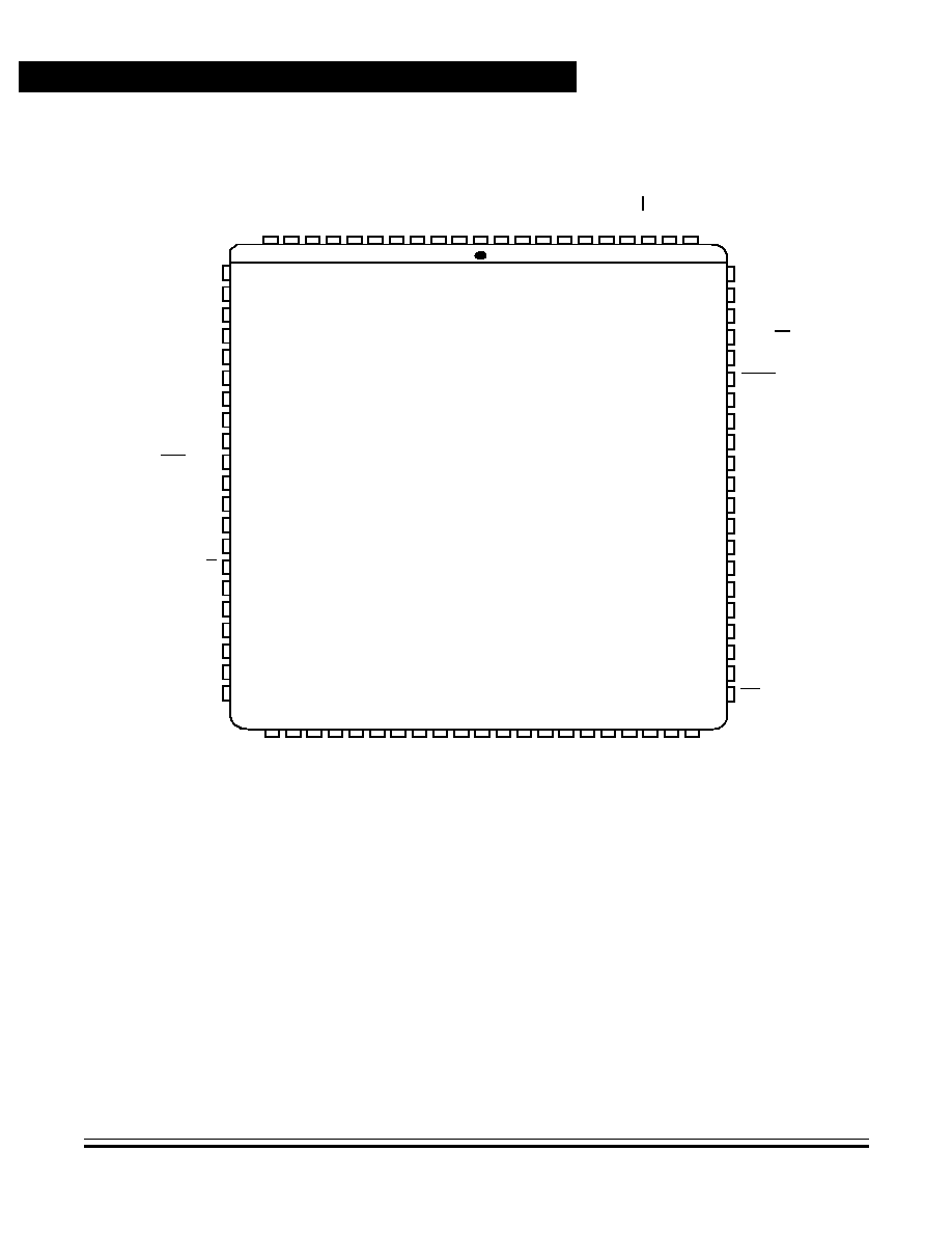
Technical Data
M68HC11K Family
32
Pin Description
MOTOROLA
Pin Description
Figure 2-1. Pin Assignments for M68HC11K 84-Pin PLCC/J-Cerquad
PD2/MISO
74
PD1/T
X
D
73
PD0/R
X
D
72
MODA/LIR
71
MODB/V
STBY
70
RESET
69
XTAL
68
EXTAL
67
XOUT
66
E
65
V
DD
64
V
SS
63
PC7/DATA7
62
PC6/DATA6
61
PC5/DATA5
60
PC4/DATA4
59
PC3/DATA3
58
PC2/DATA2
57
PC1/DATA1
56
PC0/DATA0
55
IRQ
54
PB0/
A
D
D
R
8
11
PB1A
D
D
R
9
10
P
B
2/
AD
D
R
10
9
P
B
3/
AD
D
R
11
8
PB4/
A
D
D
R
1
2
7
PB5/
A
D
D
R
1
3
6
P
B
6/
AD
D
R
14
5
P
B
7/
AD
D
R
15
4
V
SS
3
V
DD
2
PA
0
/
I
C
3
1
PA
1
/
I
C
2
84
PA2/
I
C
1
83
PA3/
I
C
4
/
OC
5/
OC
1
82
P
A
4/
OC
4/
O
C
1
81
P
A
5/
OC
3/
O
C
1
80
P
A
6
/O
C2
/O
C1
79
PA7/
PAI
/
O
C
1
78
PD
5/
S
S
77
PD
4/
S
C
K
76
PD
3/
M
O
S
I
75
PH0/PW1
PH1/PW2
PH2/PW3
PH3/PW4
PH4/CSIO
PH5/CSGP1
PH6/CSGP2
PH7/CSPROG
TEST16
(1)
XIRQ/V
PP
(2)
V
DD
V
SS
TEST14
(1)
PG7/R/W
PG6
PG5/XA18
PG4/XA17
PG3/XA16
PG2/XA15
PG1/XA14
12
13
14
15
16
17
18
19
20
21
22
23
24
25
26
27
28
29
31
32
PG0
/
XA
13
AV
DD
PE7/
A
N
7
PE6/
A
N
6
PE5/
A
N
5
PE4/
A
N
4
PE3/
A
N
3
PE2/
A
N
2
PE1/
A
N
1
PE0/
A
N
0
V
RL
V
RH
33
34
35
36
37
38
39
40
41
42
43
44
45
46
47
48
49
50
51
52
53
30
P
F
7
/
A
D
DR7
P
F
6
/
A
D
DR6
P
F
5
/
A
D
DR5
P
F
4
/
A
D
DR4
P
F
3
/
A
D
DR3
P
F
2
/
A
D
DR2
P
F
1
/
A
D
DR1
P
F
0
/
A
D
DR0
AV
SS
TEST15
(1)
1. Pins 20, 22, and 25 are used only during factory testing and should not be connected to external circuitry.
2. V
PP
applies only to EPROM devices.
Notes:
Pin Description
Introduction
M68HC11K Family
Technical Data
MOTOROLA
Pin Description
33
Figure 2-2. Pin Assignments for M6811K 80-Pin QFP
PF0/ADDR0
60
PF1/ADDR1
59
PF2/ADDR2
58
PF3/ADDR3
57
PF4/ADDR4
56
PF5/ADDR5
55
PF6/ADDR6
54
PF7/ADDR7
53
AV
SS
52
V
RH
51
V
RL
50
PE0/AN0
49
PE1/AN1
48
PE2/AN2
47
PE3/AN3
46
PE4/AN4
45
PE5/AN5
44
PE6/AN6
43
PE7/AN7
42
AV
DD
41
PD
2/
M
I
SO
80
PD
1/
T
X
D
79
PD
0/
R
X
D
78
MO
DA
/L
I
R
77
MO
DB
/V
ST
BY
76
R
E
SET
75
XT
AL
74
EXT
AL
73
E
72
V
DD
71
V
SS
70
PC
7/
D
A
T
A
7
69
PC
6/
D
A
T
A
6
68
PC
5/
D
A
T
A
5
67
PC
4/
D
A
T
A
4
66
PC
3/
D
A
T
A
3
65
PC
2/
D
A
T
A
2
64
PC
1/
D
A
T
A
1
63
PC
0/
D
A
T
A
0
62
IR
Q
61
PD3/MOSI
1
PD4/SCK
2
PD5/SS
3
PA7/PAI/OC1
4
PA6/OC2/OC1
5
PA5/OC3/OC1
6
PA4/OC4/OC1
7
PA3/IC4/OC5/OC1
8
PA2/IC1
9
PA1/IC2
10
PA0/IC3
11
V
DD
12
V
SS
13
PB7/ADDR15
14
PB6/ADDR14
15
PB5/ADDR13
16
PB4/ADDR12
17
PB3/ADDR11
18
PB2/ADDR10
19
PB1/ADDR9
20
P
B
0
/
A
DDR8
2
1
PH
0/
PW
1
2
2
PH
1/
PW
2
2
3
PH
2/
PW
3
2
4
PH
3/
PW
4
2
5
PH
4/
C
S
I
O
2
6
PH
5
/
C
S
GP
1
2
7
PH
6
/
C
S
GP
2
2
8
PH
7/
C
S
P
R
O
G
29
XI
R
Q
/V
PP
*
30
V
DD
31
V
SS
32
PG7/
R
/
W
33
PG
6
3
4
PG5/
XA
18
35
PG4/
XA
17
36
PG3/
XA
16
37
PG2/
XA
15
38
PG1/
XA
14
39
PG0/
XA
13
40
* V
PP
applies only to EPROM devices.
Technical Data
M68HC11K Family
34
Pin Description
MOTOROLA
Pin Description
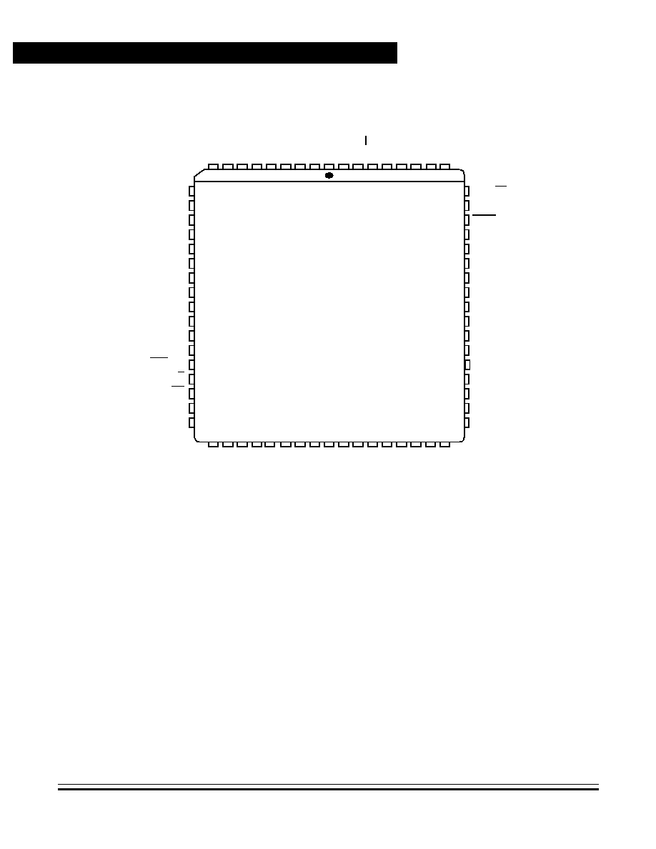
Figure 2-3. Pin Assignments for M6811KS 68-Pin PLCC/J-Cerquad
MODA/LIR
60
MODB/V
STBY
59
RESET
58
XTAL
57
EXTAL
56
XOUT
55
E
54
PC7/DATA7
53
PC6/DATA6
52
PC5/DATA5
51
PC4/DATA4
50
PC3/DATA3
49
PC2/DATA2
48
PC1/DATA1
47
PC0/DATA0
46
PF0/ADDR0
45
PF1/ADDR1
44
PA0/
I
C
3
9
PA1/
I
C
2
8
PA2/
I
C
1
7
PA3/
I
C
4
/
OC
5/
OC
1
6
P
A
4
/O
C4
/O
C1
5
P
A
5
/O
C3
/O
C1
4
P
A
6
/O
C2
/O
C1
3
PA7/
PAI
/
O
C
1
2
V
DD
1
V
DD
68
V
SS
67
PD
5/
SS
66
PD
4/
SC
K
65
PD
3/
M
O
SI
64
PD
2/
M
I
SO
63
PD
1/
T
X
D
62
PD
0/
R
X
D
61
PB7/ADDR15
PB6/ADDR14
PB5/ADDR13
PB4/ADDR12
PB3/ADDR11
PB2/ADDR10
PB1/ADDR9
PB0/ADDR8
PH1/PW2
PH2/PW3
PH3/PW4
XIRQ/V
PP
*
PG7/R/W
IRQ
AV
DD
PE7/AN7
10
11
12
13
14
15
16
17
18
19
20
21
22
23
24
25
PE
6
/
A
N
6
PE
5
/
A
N
5
PE
4
/
A
N
4
PE
3
/
A
N
3
PE
2
/
A
N
2
PE
1
/
A
N
1
PE
0
/
A
N
0
V
RL
V
RH
AV
SS
27
28
29
30
31
32
33
34
35
36
37
38
39
40
41
42
43
26
P
F
7
/
A
DDR
7
P
F
6
/
A
DDR
6
P
F
5
/
A
DDR
5
P
F
4
/
A
DDR
4
P
F
3
/
A
DDR
3
P
F
2
/
A
DDR
2
V
SS
PH0/PW1
* V
PP
applies only to EPROM devices.
Pin Description
Introduction
M68HC11K Family
Technical Data
MOTOROLA
Pin Description
35
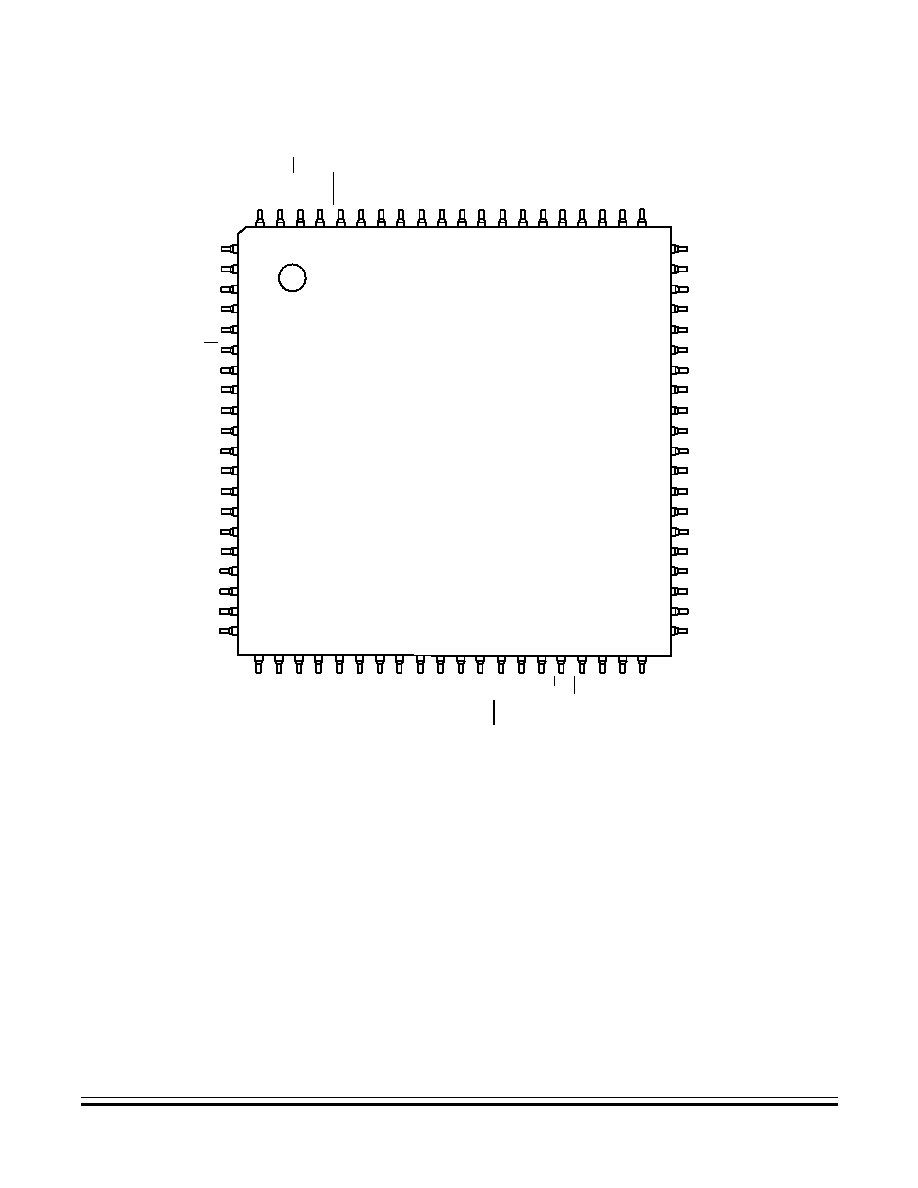
Figure 2-4. Pin Assignments for M6811KS 80-Pin LQFP
PF2/ADDR2
60
PF3/ADDR3
59
PF4/ADDR4
58
PF5/ADDR5
57
PF6/ADDR6
56
PF7/ADDR7
55
V
SS
54
AV
SS
53
V
RH
52
NC
51
V
RL
50
NC
49
PE0/AN0
48
PE1/AN1
47
PE2/AN2
46
PE3/AN3
45
PE4/AN4
44
PE5/AN5
43
PE6/AN6
42
NC
41
NC
80
NC
79
MO
DA
/L
I
R
78
MO
DB
/V
ST
BY
77
R
E
SET
76
XT
AL
75
EXT
AL
74
XOU
T
73
E
72
NC
71
PC
7/
D
A
T
A
7
70
PC
6/
D
A
T
A
6
69
PC
5/
D
A
T
A
5
68
PC
4/
D
A
T
A
4
67
PC
3/
D
A
T
A
3
66
PC
2/
D
A
T
A
2
65
PC
1/
D
A
T
A
1
64
PC
0/
D
A
T
A
0
63
P
F
0
/
A
D
DR0
62
P
F
1
/
A
D
DR1
61
PD0/RXD
1
PD1/TXD
2
PD2/MISO
3
PD3/MOSI
4
PD4/SCK
5
PD5/SS
6
NC
7
V
SS
8
NC
9
V
DD
10
NC
11
V
DD
12
PA7/PAI/OC1
13
PA6/OC2/OC1
14
PA5/OC3/OC1
15
PA4/OC4/OC1
16
PA3/IC4/OC5/OC1
17
PA2/IC1
18
PA1/IC2
19
PA0/IC3
20
P
B
7
/
A
D
D
R
15
21
P
B
6
/
A
D
D
R
14
22
P
B
5
/
A
D
D
R
13
23
P
B
4
/
A
D
D
R
12
24
P
B
3
/
A
D
D
R
11
25
P
B
2
/
A
D
D
R
10
26
P
B
1
/
A
DDR9
2
7
P
B
0
/
A
DDR8
2
8
PH
0/
PW
1
2
9
PH
1/
PW
2
3
0
PH
2/
PW
3
3
1
PH
3/
PW
4
3
2
XI
R
Q
/V
PP
*3
3
NC
3
4
NC
3
5
PG
7
/
R
/
W
36
IRQ
37
AV
DD
38
PE
7
/
A
N
7
3
9
NC
4
0
* V
PP
applies only to EPROM devices.

Technical Data
M68HC11K Family
36
Pin Description
MOTOROLA
Pin Description
2.3 Power Supply (V
DD
, V
SS
, AV
DD
, and AV
SS
)
The MCU operates from a single 5-volt (nominal) power supply. V
DD
is
the positive power input and V
SS
is ground. There are three V
DD
/V
SS
pairs of pins on the K series devices and two sets on the KS devices. All
devices contain a separate pair of power inputs, AV
DD
and AV
SS
, for the
analog-to-digital (A/D) converter, so that the A/D circuitry can be
bypassed independently.
Very fast signal transitions occur on the MCU pins. The short rise and fall
times place high, short duration current demands on the power supply.
To prevent noise problems, provide good power supply bypassing at the
MCU. Also, use bypass capacitors that have good high-frequency
characteristics and situate them as close to the MCU as possible.
Bypass requirements vary, depending on how heavily the MCU pins are
loaded.
2.4 Reset (RESET)
This active-low, bidirectional control signal acts as an input to initialize
the MCU to a known start-up state. It also serves as an open-drain
output to indicate that an internal failure has been detected in either the
clock monitor or computer operating properly (COP) watchdog circuit.
The CPU distinguishes between internal and external reset conditions
by counting the number of E-clock cycles that occur between the start of
reset and the presence of a logic 1 voltage level on the reset pin. Less
than two cycles indicates an internal reset; greater than two, an external
reset. To prevent the device from misinterpreting the kind of reset that
occurs, do not connect an external resistor-capacitor (RC) power-up
delay circuit directly to the reset pin.
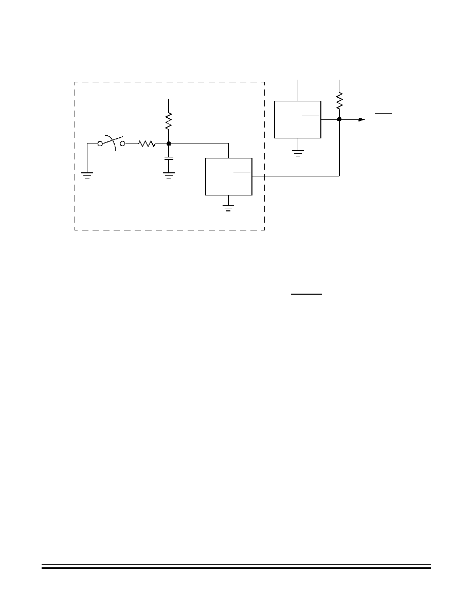
Pin Description
Crystal Driver and External Clock Input (XTAL and EXTAL)
M68HC11K Family
Technical Data
MOTOROLA
Pin Description
37
Figure 2-5. External Reset Circuit
It is important to protect the MCU against corruption of RAM and
EEPROM during power transitions. This can be done with a low-voltage
interrupt (LVI) circuit which holds the RESET pin low when V
DD
drops
below the minimum operating level.
Figure 2-5
shows a suggested reset
circuit that incorporates two LVI devices and an external switch.
2.5 Crystal Driver and External Clock Input (XTAL and EXTAL)
These two pins provide the interface for either a crystal or a
CMOS-compatible clock to control the internal clock generator circuitry.
The frequency applied to these pins is four times higher than the desired
E-clock rate.
When an external CMOS-compatible clock input is connected to the
EXTAL pin, the XTAL pin must be left unterminated.
CAUTION:
In all cases, use caution around the oscillator pins.
Load capacitances shown in
Figure 2-6
are specified by the crystal
manufacturer and should include all stray layout capacitances.
TO RESET
V
DD
MC34064
RESET
GND
IN
OF M68HC11
RESET
GND
IN
MANUAL
RESET SWITCH
4.7 k
1.0
�
MC34164
OPTIONAL POWER-ON DELAY AND MANUAL RESET SWITCH
V
DD
V
DD
4.7 k
4.7 k
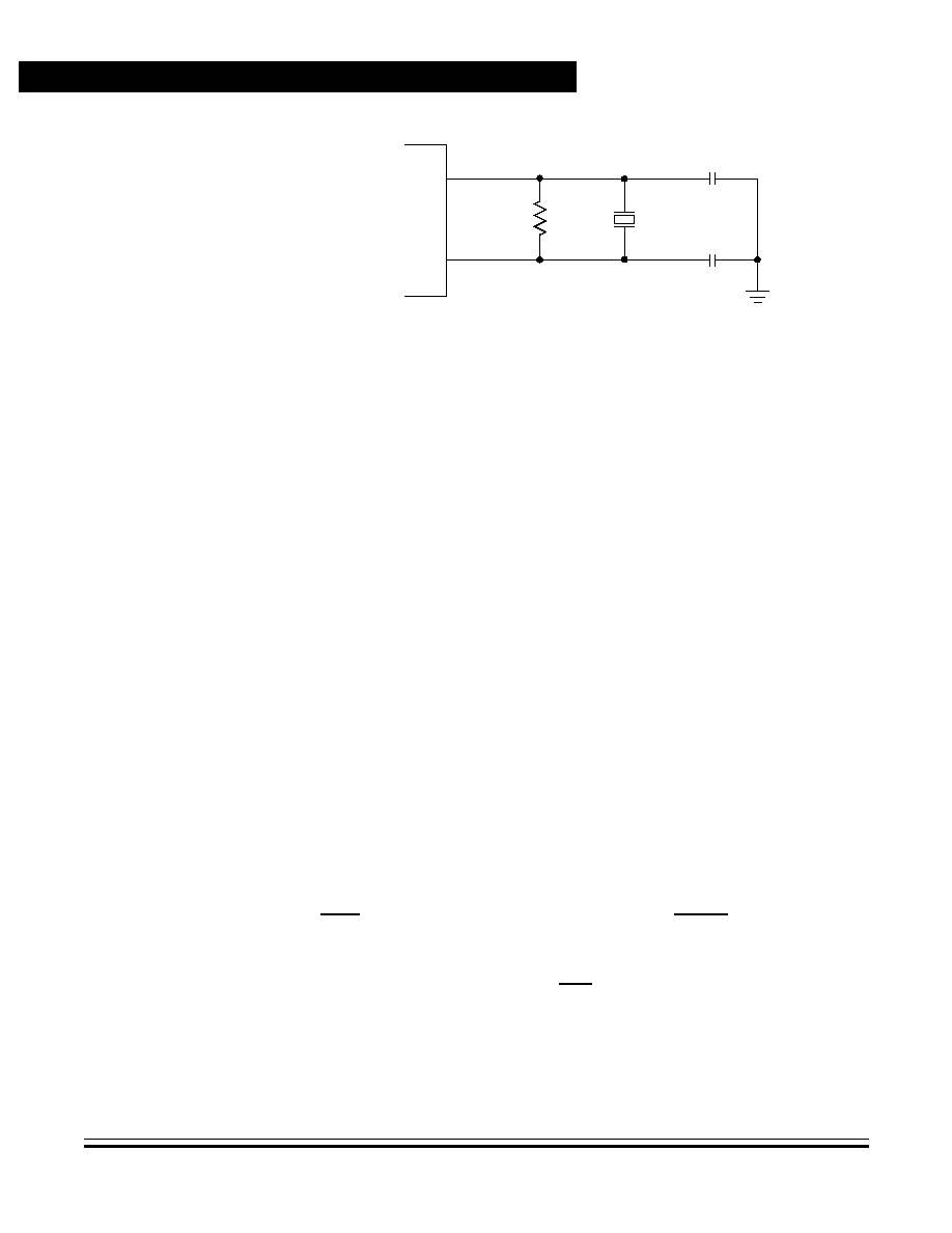
Technical Data
M68HC11K Family
38
Pin Description
MOTOROLA
Pin Description
Figure 2-6. Common Crystal Connections
2.6 XOUT
The XOUT pin provides a buffered clock signal if enabled to synchronize
external devices with the MCU. See
4.9 XOUT Pin Control
.
NOTE:
This signal is not present on the 80-pin M68HC(7)11K device QFP
package.
2.7 E-Clock Output (E)
The internally generated instruction cycle clock, or E clock, is available
on the E pin as a timing reference. Its frequency is one fourth the input
frequency at the XTAL and EXTAL pins. The E clock is low during the
address portion of a bus cycle and high during the data access portion
of the bus cycle. All clocks, including the E clock, are halted when the
MCU is in stop mode. The E-pin driver can be turned off in single-chip
modes to reduce radio frequency interference (RFI) and current
consumption.
2.8 Interrupt Request (IRQ) and Non-Maskable Interrupt (XIRQ)
The MCU provides two pins for applying asynchronous interrupt
requests. Interrupts applied to the IRQ pin can be masked by setting the
I bit in the condition code register (CCR), which can be set or cleared by
software at any time. Triggering is level sensitive by default, which is
10 M
MCU
C
L
*
C
L
*
EXTAL
XTAL
4 x E
CRYSTAL
* This value includes all stray capacitances.

Pin Description
Mode Selection, Instruction Cycle Reference, and Standby Power (MODA/LIR and MODB/VSTBY)
M68HC11K Family
Technical Data
MOTOROLA
Pin Description
39
required for wire-OR configuration. Software can change the triggering
to edge sensitive.
XIRQ interrupts can be non-maskable after reset initialization. Out of
reset, the X bit in the CCR is set, masking XIRQ interrupts. Once
software clears the X bit, it cannot be reset, and the XIRQ interrupts
become non-maskable. The XIRQ input is level sensitive only. XIRQ is
often used as a power-loss detect interrupt.
Whenever IRQ or XIRQ is used with multiple interrupt sources, each
source must drive the interrupt input with an open-drain type of driver to
avoid contention between outputs. There should be a single pullup
resistor near the MCU interrupt pin (typically 4.7 k
). There must also be
an interlock mechanism at each interrupt source which holds the
interrupt line low until the MCU recognizes and acknowledges the
interrupt request. If any interrupt sources are still pending after the MCU
services a request, the interrupt line will remain low, interrupting the
MCU again as soon as the I bit in the MCU is cleared (normally upon
return from an interrupt). Interrupt mechanisms are explained further in
Section 5. Resets and Interrupts
.
On EPROM devices, the XIRQ pin also functions as the high-voltage
supply, V
PP
, during EPROM or OTPROM programming.
CAUTION:
Ensure that the voltage level at this pin is equal to V
DD
during normal
operation to avoid programming accidents.
2.9 Mode Selection, Instruction Cycle Reference, and Standby Power
(MODA/LIR and MODB/V
STBY
)
During reset, MODA and MODB select one of four operating modes:
1. Single-chip
2. Expanded
3. Bootstrap
4. Special test
For full descriptions of these modes, refer to
4.5 Operating Modes
.
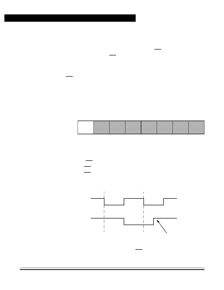
Technical Data
M68HC11K Family
40
Pin Description
MOTOROLA
Pin Description
In single-chip and bootstrap modes, the MODA pin typically is grounded
and has no function after reset. In expanded and special test modes,
MODA is normally connected to V
DD
through a 4.7-k
pullup resistor
and functions as the load instruction register (LIR) pin after reset. The
open-drain, active-low LIR output drives low during the first E-clock cycle
of each instruction (opcode fetch), providing a useful signal for system
debugging.
LIR can be driven high for a portion of each instruction cycle by setting
the LIRDV bit in the system configuration options 2 (OPT2) register (see
Figure 2-7
and
Figure 2-8
). This feature can help detect consecutive
instructions and prevent false triggering in high-speed applications.
LIRDV -- LIR Driven Bit
0 = LIR not driven high
1 = LIR driven high for one quarter cycle to reduce transition time
Figure 2-8. LIR Timing
Address: $0038
Bit 7
6
5
4
3
2
1
Bit 0
Read:
LIRDV
CWOM
STRCH
(1)
IRVNE
LSBF
SPR2
XDV1
XDV0
Write:
Reset:
0
0
0
--
0
0
0
0
1. STRCH is not available on K devices.
Figure 2-7. System Configuration Options 2 (OPT2)
E
LIR
LAST CYCLE OF
FIRST CYCLE OF NEW
OPCODE FETCH
Note: If LIRDV is not set, the pullup resistor may
not return the level to a logic 1 before
INSTRUCTION
PREVIOUS INSTRUCTION
the next data fetch.
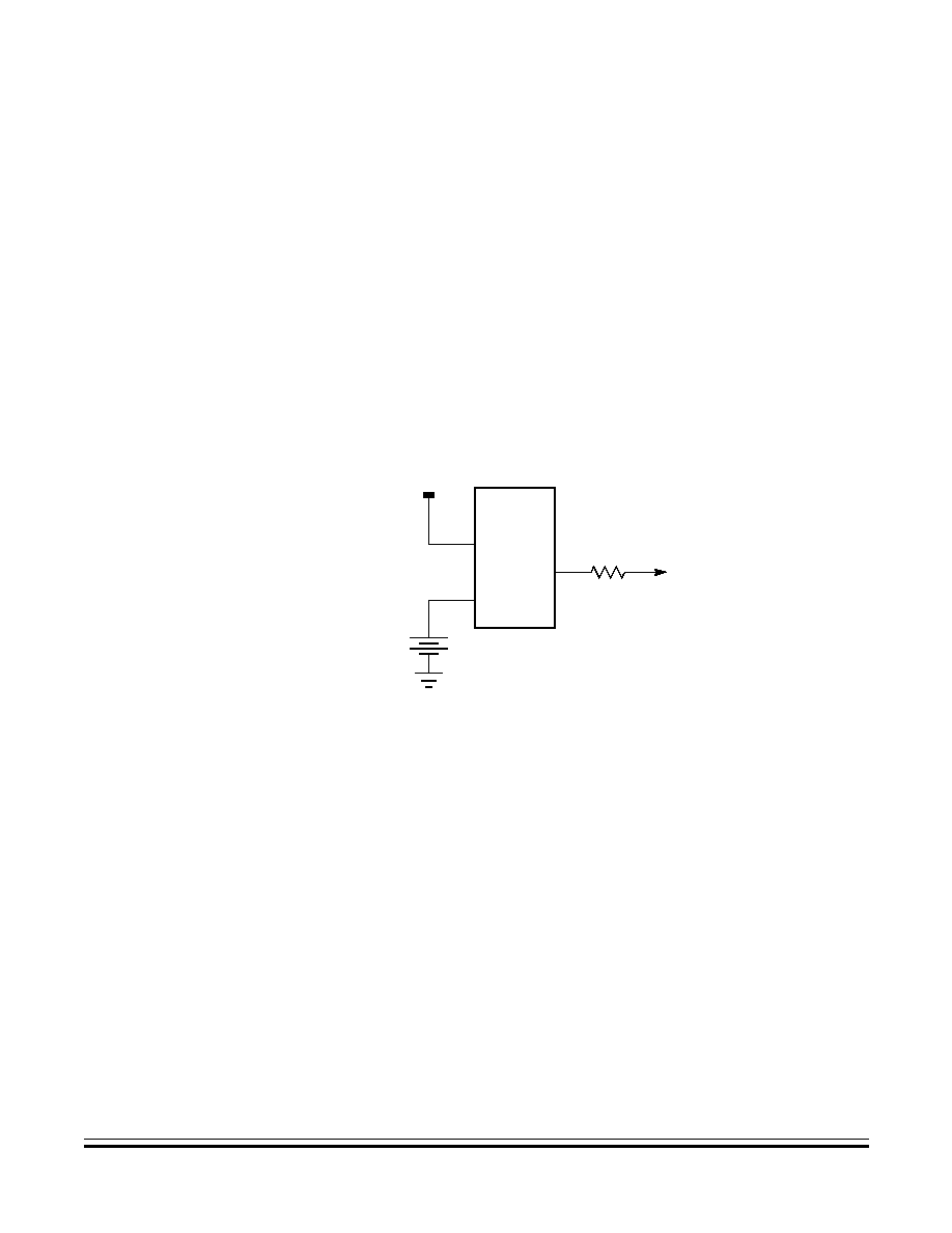
Pin Description
VRH and VRL
M68HC11K Family
Technical Data
MOTOROLA
Pin Description
41
The MODB pin is grounded to select special modes, and has no function
after reset. To select the normal operating modes (single-chip and
expanded) the MODB pin is pulled to a logic high level. Connecting
MODB to a voltage source other than V
DD
enables it to function as a
battery backup input, V
STBY.
When V
DD
drops more than one MOS
threshold (about 0.7 volts) below the voltage at V
STBY
,
the MCU's RAM
and part of the reset logic are powered from V
STBY
rather than V
DD
.
Reset must be driven low before V
DD
is removed and must remain low
until V
DD
has been restored to a valid level. The extra hardware required
to utilize V
STBY
may be justified in certain applications where a
significant amount of external circuitry operates from V
DD
.
Figure 2-9
shows a suggested circuit employing the V
STBY
pin.
Figure 2-9. MODB/V
STBY
Connection
2.10 V
RH
and V
RL
These pins provide the reference voltage for the analog-to-digital
converter.
2.11 Port Signals
The K series contains 62 input/output lines arranged in eight ports, A
through H; all ports are eight bits except port D, which is six bits. The KS
series drops seven lines from port G and four from port H, for a total of
4.7 K
MAX
690
V
BATT
+
4.8 V
NICD
V
DD
V
DD
V Out
TO MODB/ V
STBY
OF M68HC11

Technical Data
M68HC11K Family
42
Pin Description
MOTOROLA
Pin Description
51 I/O lines. All ports are fully bidirectional except port E, which is input
only.
Each port can serve as either general-purpose I/O or as part of the
microcontroller's specialized functions, depending on the operating
mode or peripheral functions selected. The functions of ports B, C, and
F and port G bit 7 depend on the operating mode. They serve as
general-purpose I/O lines in single-chip and bootstrap modes and
provide the address and data buses in expanded and special test
modes. The other ports serve as general-purpose I/O out of reset; writes
to control registers enable their special functions.
Section 6. Parallel
Input/Output
describes general-purpose I/O operation in detail.
Table 2-1
summarizes the ports and references for peripheral functions.
Table 2-2
summarizes the port signals.
Table 2-1. I/O Ports and Peripheral Functions
I/O Port
Special Function(s)
Enabled by
Refer to
Port A
Timer and
pulse accumulator
Control registers
Section 9. Timing System
Port B
High-order
address bus
Expanded
operating modes
Section 4. Operating Modes and On-Chip Memory
Port C
Data bus
Expanded
operating modes
Section 4. Operating Modes and On-Chip Memory
Port D
Serial communication
interface and
Serial peripheral
interface
Control registers
Section 7. Serial Communications Interface (SCI)
and
Section 8. Serial Peripheral Interface (SPI)
Port E
A/D converter
Control registers
Section 10. Analog-to-Digital (A/D) Converter
Port F
Low-order
address bus
Expanded
operating modes
Section 4. Operating Modes and On-Chip Memory
Port G
bit 7
bits 6�0
(1)
R/W line
and expansion
address lines
Expanded
operating modes
and
control registers
(2)
Section 4. Operating Modes and On-Chip Memory
and
Section 11. Memory Expansion and Chip Selects
Port H
bits 7�4
(1)
bits 3�0
Chip-select lines
and
pulse-width modulator
Control registers
Section 9. Timing System
and
Section 11. Memory Expansion and Chip Selects
1. Not available on KS devices
2. Control registers can enable these functions only in expanded operating modes.
Pin Description
Port Signals
M68HC11K Family
Technical Data
MOTOROLA
Pin Description
43
Table 2-2. Port Signal Summary
Port/Bit
Single-Chip and
Bootstrap Modes
Expanded and
Special Test Modes
PA0
PA0/IC3
PA1
PA1/IC2
PA2
PA2/IC1
PA3
PA3/OC5/IC4/and-or OC1
PA4
PA4/OC4/and-or OC1
PA5
PA5/OC3/and-or OC1
PA6
PA6/OC2/and-or OC1
PA7
PA7/PAI/and-or OC1
PB[7:0]
PB[7:0]
ADDR[15:8]
PC[7:0]
PC[7:0]
DATA[7:0]
PD0
PD0/RxD
PD1
PD1/TxD
PD2
PD2/MISO
PD3
PD3/MOSI
PD4
PD4/SCK
PD5
PD5/SS
PE[7:0]
PE[7:0]/AN[7:0]
PF[7:0]
PF[7:0]
ADDR[7:0]
PG0
PG0
PG0/XA13
PG1
PG1
PG1/XA14
PG2
PG2
PG2/XA15
PG3
PG3
PG3/XA16
PG4
PG4
PG4/XA17
PG5
PG5
PG5/XA18
PG6
PG6
PG6
PG7
PG7
PG7/R/W
PH0
PH0/PW1
PH1
PH1/PW2
PH2
PH2/PW3
PH3
PH3/PW4
PH4
PH4
PH4/CSIO
PH5
PH5
PH5/CSGP1
PH6
PH6
PH6/CSGP2
PH7
PH7
PH7/CSPROG

Technical Data
M68HC11K Family
44
Pin Description
MOTOROLA
Pin Description

M68HC11K Family
Technical Data
MOTOROLA
Central Processor Unit (CPU)
45
Technical Data -- M68HC11K Family
Section 3. Central Processor Unit (CPU)
3.1 Contents
3.2
Introduction . . . . . . . . . . . . . . . . . . . . . . . . . . . . . . . . . . . . . . . . 46
3.3
CPU Registers . . . . . . . . . . . . . . . . . . . . . . . . . . . . . . . . . . . . . 46
3.3.1
Accumulators A, B, and D (ACCA, ACCB, and ACCD) . . . . 47
3.3.2
Index Register X (IX) . . . . . . . . . . . . . . . . . . . . . . . . . . . . . . 47
3.3.3
Index Register Y (IY) . . . . . . . . . . . . . . . . . . . . . . . . . . . . . . 47
3.3.4
Stack Pointer (SP) . . . . . . . . . . . . . . . . . . . . . . . . . . . . . . . . 48
3.3.5
Program Counter (PC) . . . . . . . . . . . . . . . . . . . . . . . . . . . . .50
3.3.6
Condition Code Register (CCR) . . . . . . . . . . . . . . . . . . . . . . 50
3.3.6.1
Carry/Borrow (C) . . . . . . . . . . . . . . . . . . . . . . . . . . . . . . . 50
3.3.6.2
Overflow (V) . . . . . . . . . . . . . . . . . . . . . . . . . . . . . . . . . . . 50
3.3.6.3
Zero (Z) . . . . . . . . . . . . . . . . . . . . . . . . . . . . . . . . . . . . . .50
3.3.6.4
Negative (N) . . . . . . . . . . . . . . . . . . . . . . . . . . . . . . . . . . . 51
3.3.6.5
Interrupt Mask (I) . . . . . . . . . . . . . . . . . . . . . . . . . . . . . . . 51
3.3.6.6
Half Carry (H) . . . . . . . . . . . . . . . . . . . . . . . . . . . . . . . . . .51
3.3.6.7
Non-Maskable Interrupt (X) . . . . . . . . . . . . . . . . . . . . . . . 52
3.3.6.8
Stop Disable (S) . . . . . . . . . . . . . . . . . . . . . . . . . . . . . . . . 52
3.4
Data Types . . . . . . . . . . . . . . . . . . . . . . . . . . . . . . . . . . . . . . . . 52
3.5
Opcodes and Operands . . . . . . . . . . . . . . . . . . . . . . . . . . . . . . 53
3.6
Addressing Modes . . . . . . . . . . . . . . . . . . . . . . . . . . . . . . . . . . 53
3.6.1
Immediate. . . . . . . . . . . . . . . . . . . . . . . . . . . . . . . . . . . . . . . 54
3.6.2
Direct . . . . . . . . . . . . . . . . . . . . . . . . . . . . . . . . . . . . . . . . . . 54
3.6.3
Extended . . . . . . . . . . . . . . . . . . . . . . . . . . . . . . . . . . . . . . . 54
3.6.4
Indexed. . . . . . . . . . . . . . . . . . . . . . . . . . . . . . . . . . . . . . . . . 54
3.6.5
Inherent . . . . . . . . . . . . . . . . . . . . . . . . . . . . . . . . . . . . . . . . 55
3.6.6
Relative . . . . . . . . . . . . . . . . . . . . . . . . . . . . . . . . . . . . . . . . 55
3.7
Instruction Set. . . . . . . . . . . . . . . . . . . . . . . . . . . . . . . . . . . . . .55
Technical Data
M68HC11K Family
46
Central Processor Unit (CPU)
MOTOROLA
Central Processor Unit (CPU)
3.2 Introduction
This section presents information on M68HC11 central processor unit
(CPU) architecture, data types, addressing modes, the instruction set,
and special operations, such as subroutine calls and interrupts.
The CPU employs memory-mapped input/output (I/O). There are no
special instructions for I/O; all peripheral, I/O, and memory locations are
simply addresses in the 64-Kbyte memory map. This architecture also
enables access to operands from external memory locations with no
execution time penalty.
3.3 CPU Registers
M68HC11 CPU registers are an integral part of the CPU and are not
addressed as memory locations. The seven registers are shown in
Figure 3-1
.
Figure 3-1. Programming Model
8-BIT ACCUMULATORS A & B
7
0
7
0
15
0
A
B
D
IX
IY
SP
PC
7
0
C
V
Z
N
I
H
X
S
OR 16-BIT DOUBLE ACCUMULATOR D
INDEX REGISTER X
INDEX REGISTER Y
STACK POINTER
PROGRAM COUNTER
CARRY/BORROW FROM MSB
OVERFLOW
ZERO
NEGATIVE
I-INTERRUPT MASK
HALF CARRY (FROM BIT 3)
X-INTERRUPT MASK
STOP DISABLE
CONDITION CODES

Central Processor Unit (CPU)
CPU Registers
M68HC11K Family
Technical Data
MOTOROLA
Central Processor Unit (CPU)
47
3.3.1 Accumulators A, B, and D (ACCA, ACCB, and ACCD)
Accumulators A and B are general-purpose 8-bit registers that hold
operands and results of arithmetic calculations or data manipulations.
Some instructions treat these two accumulators as a single double-byte
(16-bit) accumulator called accumulator D. Most operations can use
either accumulator A or B, with these exceptions:
�
The ABX and ABY instructions add the contents of 8-bit
accumulator B to the contents of 16-bit register X or Y, but there
are no equivalent instructions that use A instead of B.
�
The TAP and TPA instructions transfer data from accumulator A
to the condition code register or from the condition code register
to accumulator A. However, there are no equivalent instructions
that use B rather than A.
�
The DAA instruction adjusts accumulator A after binary-coded
decimal (BCD) arithmetic operations, but there is no equivalent
BCD instruction to adjust accumulator B.
�
The add, subtract, and compare instructions associated with both
A and B (ABA, SBA, and CBA) only operate in one direction,
making planning ahead important to ensure the correct operand is
in the correct accumulator.
3.3.2 Index Register X (IX)
The IX register provides a 16-bit indexing value that can be added to the
8-bit offset provided in an instruction to create an effective address. The
IX register can be used also as a counter or as a temporary storage
register.
3.3.3 Index Register Y (IY)
The IY register provides a 16-bit indexed mode function similar to that of
the IX register. Instructions using the IY register require an extra byte of
machine code and an extra cycle of execution time because of the way
the opcode map is implemented.

Technical Data
M68HC11K Family
48
Central Processor Unit (CPU)
MOTOROLA
Central Processor Unit (CPU)
3.3.4 Stack Pointer (SP)
The stack pointer holds the 16-bit address of the next free location in the
M68HC11 CPU's automatic program stack. This stack is a data structure
that grows downward from high memory to low memory. The stack can
be located anywhere in the address space and can be any size up to the
amount of memory available in the system. Most application programs
initialize the SP at the beginning of an application program with a load
stack (LDS) instruction. Thereafter, each time the CPU pushes a new
byte onto the stack, it decrements the SP. To pull a byte from the stack,
the CPU first increments the SP.
Figure 3-2
is a summary of SP
operations.
A jump-to-subroutine (JSR) or branch-to-subroutine (BSR) instruction
pushes the address of the instruction immediately after the JSR or BSR
onto the stack, least significant byte first. The last instruction of the
subroutine is a return-from-subroutine (RTS), which pulls the previously
stored return address from the stack and loads it into the program
counter. Execution then continues at this recovered return address.
When the processor recognizes an interrupt, it finishes the current
instruction, pushes the return address (the current value in the program
counter) onto the stack, pushes all of the CPU registers onto the stack,
and continues at the address specified by the vector for the interrupt.
The interrupt service routine ends with a return-from-interrupt (RTI)
instruction, which pulls the saved registers off the stack in reverse order.
Program execution resumes at the return address with all register
contents restored.
There are instructions that push and pull the A and B accumulators and
the X and Y index registers to preserve program context. For example,
push accumulator A onto the stack when entering a subroutine that uses
accumulator A, and pull accumulator A off the stack just before leaving
the subroutine, to ensure that the contents of that register will be the
same after returning from the subroutine as it was before starting the
subroutine.
Central Processor Unit (CPU)
CPU Registers
M68HC11K Family
Technical Data
MOTOROLA
Central Processor Unit (CPU)
49
Figure 3-2. Stacking Operations
SP�2
STACK
RTN
H
SP�1
RTN
L
SP
7
0
PC
MAIN PROGRAM
$9D = JSR
JSR, JUMP TO SUBROUTINE
dd
NEXT MAIN INSTR.
RTN
DIRECT
PC
MAIN PROGRAM
$AD = JSR
ff
NEXT MAIN INSTR.
RTN
INDEXED, X
PC
MAIN PROGRAM
$18 = PRE
ff
NEXT MAIN INSTR.
RTN
INDEXED, Y
$AD = JSR
PC
MAIN PROGRAM
$BD = PRE
ll
NEXT MAIN INSTR.
RTN
INDEXED, Y
hh
SP
STACK
CCR
SP+1
ACCB
SP+2
ACCA
SP+3
IX
H
SP+4
IX
L
SP+5
IY
H
SP+6
IY
L
SP+7
RTN
H
SP+8
SP+9
7
0
RTN
L
PC
INTERRUPT ROUTINE
$3B = RTI
SP�9
STACK
CCR
SP�8
ACCB
SP�7
ACCA
SP�6
IX
H
SP�5
IX
L
SP�4
IY
H
SP�3
IY
L
SP�2
RTN
H
SP�1
SP
7
0
RTN
L
PC
MAIN PROGRAM
$3F = SWI
PC
MAIN PROGRAM
$3E = WAI
SWI, SOFTWARE INTERRUPT
WAI, WAIT FOR INTERRUPT
RTI, RETURN FROM INTERRUPT
SP�2
STACK
RTN
H
SP�1
RTN
L
SP
7
0
PC
MAIN PROGRAM
$8D = BSR
PC
MAIN PROGRAM
$39 = RTS
BSR, BRANCH TO SUBROUTINE
RTS, RETURN FROM
SUBROUTINE
SP
STACK
RTN
H
SP+1
RTN
L
SP+2
7
0
LEGEND:
RTN = ADDRESS OF NEXT INSTRUCTION IN MAIN PROGRAM TO
BE EXECUTED UPON RETURN FROM SUBROUTINE
RTN
H
= MOST SIGNIFICANT BYTE OF RETURN ADDRESS
RTN
L
= LEAST SIGNIFICANT BYTE OF RETURN ADDRESS
= STACK POINTER POSITION AFTER OPERATION IS COMPLETE
dd = 8-BIT DIRECT ADDRESS ($0000�$00FF) (HIGH BYTE ASSUMED
TO BE $00)
ff = 8-BIT POSITIVE OFFSET $00 (0) TO $FF (255) IS ADDED TO INDEX
hh = HIGH-ORDER BYTE OF 16-BIT EXTENDED ADDRESS
ll = LOW-ORDER BYTE OF 16-BIT EXTENDED ADDRESS
rr= SIGNED RELATIVE OFFSET $80 (�128) TO $7F (+127) (OFFSET
RELATIVE TO THE ADDRESS FOLLOWING THE MACHINE CODE
OFFSET BYTE)

Technical Data
M68HC11K Family
50
Central Processor Unit (CPU)
MOTOROLA
Central Processor Unit (CPU)
3.3.5 Program Counter (PC)
The 16-bit program counter contains the address of the next instruction
to be executed. Its initial value after reset is fetched from one of six
possible vectors, depending on operating mode and the cause of reset,
as described in
5.3 Sources of Resets
.
3.3.6 Condition Code Register (CCR)
This 8-bit register contains:
�
Five condition code indicators (C, V, Z, N, and H)
�
Two interrupt masking bits (IRQ and XIRQ)
�
A stop disable bit (S)
Most instructions update condition codes automatically, as described in
the following paragraphs. Certain instructions, such as pushes, pulls,
add B to X (ABX), add B to Y (ABY), and transfer/exchange instructions
do not affect the condition codes.
Table 3-1
shows which condition
codes are affected by each instruction.
3.3.6.1 Carry/Borrow (C)
The C bit is set if the CPU performs a carry or borrow during an
arithmetic operation. This bit also acts as an error flag for multiply and
divide operations. Shift and rotate instructions operate with and through
the carry bit to facilitate multiple-word shift operations.
3.3.6.2 Overflow (V)
The overflow bit is set if an operation results in a two's complement
overflow of the 8-bit signed range �128 to +127. Otherwise, the V bit is
cleared.
3.3.6.3 Zero (Z)
The Z bit is set if the result of an arithmetic, logic, or data manipulation
operation is 0. Otherwise, the Z bit is cleared. Compare instructions do

Central Processor Unit (CPU)
CPU Registers
M68HC11K Family
Technical Data
MOTOROLA
Central Processor Unit (CPU)
51
an internal implied subtraction and the condition codes, including Z,
reflect the results of that subtraction. A few operations (INX, DEX, INY,
and DEY) affect the Z bit and no other condition flags.
3.3.6.4 Negative (N)
The N bit is set if the result of an arithmetic, logic, or data manipulation
operation is negative, meaning that the most significant bit (MSB) of the
result is a 1. Otherwise, the N bit is cleared. To determine quickly if the
MSB of a particular byte is set, load it into an accumulator and then
check the status of the N bit.
3.3.6.5 Interrupt Mask (I)
When the interrupt mask bit is set, it disables all maskable interrupt
requests (IRQs). The CPU continues to operate uninterrupted while
interrupts remain pending until the I bit is cleared. Every reset sets the
I bit by default and only a software instruction can clear it. When the
processor recognizes an interrupt, it stacks the registers, sets the I bit,
and then fetches the interrupt vector. The final instruction of an interrupt
service routine is usually a return from interrupt (RTI), which restores the
registers to the values that were present before the interrupt occurred
and clears the I bit.
NOTE:
Although the I bit can be cleared earlier in the interrupt service routine,
avoid nesting interrupts in this way without a clear understanding of
latency and of the arbitration mechanism.
Refer to
Section 5. Resets and Interrupts
.
3.3.6.6 Half Carry (H)
The H bit is set when a carry occurs between bits 3 and 4 of the
arithmetic logic unit during an ADD, ABA, or ADC instruction. Otherwise,
the H bit is cleared. Half carry is used during binary-coded decimal
(BCD) operations.

Technical Data
M68HC11K Family
52
Central Processor Unit (CPU)
MOTOROLA
Central Processor Unit (CPU)
3.3.6.7 Non-Maskable Interrupt (X)
Setting the XIRQ mask (X) bit disables non-maskable interrupts from the
XIRQ pin. Every reset sets the X bit by default and only a software
instruction can clear it. When the processor recognizes a non-maskable
interrupt, it stacks the registers, sets the X and I bits, and then fetches
the interrupt vector. An interrupt service routine usually ends with a
return from interrupt (RTI), which restores the registers to the values that
were present before the interrupt occurred and clears the X bit. Only
hardware or an acknowledge can set the X bit. Only software can clear
the X bit (for example, the TAP instruction which transfers data from
accumulator A to the condition code register). There is no hardware
action for clearing X.
3.3.6.8 Stop Disable (S)
Setting the STOP disable (S) bit prevents the STOP instruction from
putting the M68HC11 into a low-power stop condition. If the S bit is set,
the CPU treats a STOP instruction as if it were a no-operation (NOP)
instruction and continues to the next instruction.
NOTE:
S is set by reset and STOP is disabled by default.
The STOP instruction can be cleared by using the TAP instruction which
transfers data from accumulator A to the condition code register.
3.4 Data Types
The MC68HC11 CPU supports these data types:
�
Bit data
�
8-bit and 16-bit signed and unsigned integers
�
16-bit unsigned fractions
�
16-bit addresses
A byte is eight bits wide and can be accessed at any byte location. A
word is composed of two consecutive bytes with the most significant
byte at the lower value address. Because the M68HC11 is an 8-bit CPU,

Central Processor Unit (CPU)
Opcodes and Operands
M68HC11K Family
Technical Data
MOTOROLA
Central Processor Unit (CPU)
53
there are no special requirements for alignment of instructions or
operands.
3.5 Opcodes and Operands
The M68HC11 Family of microcontrollers uses 8-bit opcodes. Every
instruction requires a unique opcode for each of its addressing modes.
The resulting number of opcodes exceeds the 256 available in an 8-bit
binary number. A 4-page opcode map has been implemented to
accommodate the extra instructions. An additional byte, called a
prebyte, directs the processor from page 0 of the opcode map to one of
the other three pages. As its name implies, the additional byte precedes
the opcode.
A complete instruction consists of a prebyte, if any, an opcode, and zero
to three operands. The operands contain information the CPU needs for
executing the instruction. Complete instructions can be from one to five
bytes long.
3.6 Addressing Modes
Six addressing modes can be used to access memory:
1. Immediate
2. Direct
3. Extended
4. Indexed
5. Inherent
6. Relative
All modes except inherent mode use an effective address. The effective
address is the memory address where the argument is fetched or stored
or the address from which execution is to proceed. The effective address
can be specified within an instruction or it can be calculated.

Technical Data
M68HC11K Family
54
Central Processor Unit (CPU)
MOTOROLA
Central Processor Unit (CPU)
3.6.1 Immediate
In the immediate addressing mode, the byte(s) immediately following the
opcode contain the arguments. The number of bytes following the
opcode matches the size of the register or memory location being used.
Immediate instructions can be two, three, or (if a prebyte is required) four
bytes.
3.6.2 Direct
In the direct addressing mode, the user specifies only the low-order byte
of the effective address in a single byte following the opcode. The
processor assumes the high-order byte of the address to be $00. Thus,
the CPU accesses addresses $00�$FF directly, using 2-byte
instructions. This reduces execution time by eliminating the additional
memory access required for the high-order address byte. Most
applications reserve this 256-byte area for frequently referenced data,
but various combinations of internal registers, RAM, or external memory
can occupy these addresses.
3.6.3 Extended
In the extended addressing mode, the two bytes following the opcode
byte contain the effective address of the argument. For this reason,
instructions are three bytes, or they are four bytes if a prebyte is
required.
3.6.4 Indexed
In the indexed addressing mode, the CPU computes the effective
address of the argument by adding an 8-bit unsigned offset to the value
contained in an index register (IX or IY). Any memory location in the
64-Kbyte address space can be accessed with this mode. The
instructions are from two to five bytes.

Central Processor Unit (CPU)
Instruction Set
M68HC11K Family
Technical Data
MOTOROLA
Central Processor Unit (CPU)
55
3.6.5 Inherent
In the inherent addressing mode, the opcode contains all required
information. The operands (if any) are registers, so no memory access
is required. This mode includes:
�
Control instructions with no arguments
�
Operations that only involve the index registers or accumulators
These instructions are one or two bytes.
3.6.6 Relative
Only branch instructions use the relative addressing mode. If the branch
condition is true, the CPU adds the 8-bit signed offset following the
opcode to the contents of the program counter to form the effective
branch address. Otherwise, control proceeds to the next instruction.
These are usually 2-byte instructions.
3.7 Instruction Set
Table 3-1
presents a detailed listing of all the M68HC11 instructions in
all possible addressing modes.
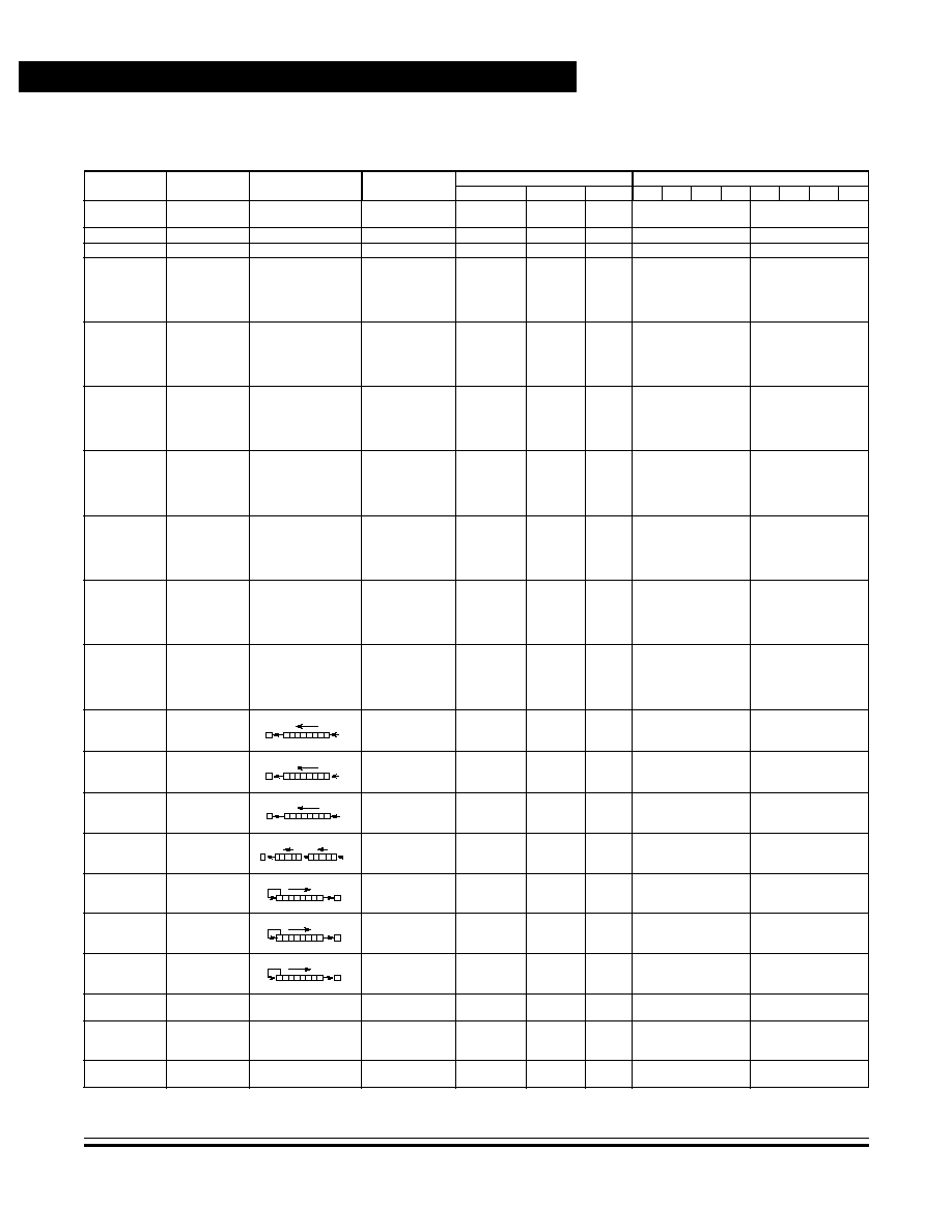
Technical Data
M68HC11K Family
56
Central Processor Unit (CPU)
MOTOROLA
Central Processor Unit (CPU)
Table 3-1. Instruction Set (Sheet 1 of 7)
Mnemonic
Operation
Description
Addressing
Instruction
Condition Codes
Mode Opcode
Operand
Cycles
S
X
H
I
N
Z
V
C
ABA
Add
Accumulators
A + B
A
INH
1B
--
2
--
--
--
ABX
Add B to X
IX + (00 : B)
IX
INH
3A
--
3
--
--
--
--
--
--
--
--
ABY
Add B to Y
IY + (00 : B)
IY
INH
18
3A
--
4
--
--
--
--
--
--
--
--
ADCA (opr)
Add with Carry
to A
A + M + C
A
A
IMM
A
DIR
A
EXT
A
IND,X
A
IND,Y
89
99
B9
A9
18
A9
ii
dd
hh ll
ff
ff
2
3
4
4
5
--
--
--
ADCB (opr)
Add with Carry
to B
B + M + C
B
B
IMM
B
DIR
B
EXT
B
IND,X
B
IND,Y
C9
D9
F9
E9
18
E9
ii
dd
hh ll
ff
ff
2
3
4
4
5
--
--
--
ADDA (opr)
Add Memory to
A
A + M
A
A
IMM
A
DIR
A
EXT
A
IND,X
A
IND,Y
8B
9B
BB
AB
18
AB
ii
dd
hh ll
ff
ff
2
3
4
4
5
--
--
--
ADDB (opr)
Add Memory to
B
B + M
B
B
IMM
B
DIR
B
EXT
B
IND,X
B
IND,Y
CB
DB
FB
EB
18
EB
ii
dd
hh ll
ff
ff
2
3
4
4
5
--
--
--
ADDD (opr)
Add 16-Bit to D
D + (M : M + 1)
D
IMM
DIR
EXT
IND,X
IND,Y
C3
D3
F3
E3
18 E3
jj kk
dd
hh ll
ff
ff
4
5
6
6
7
--
--
--
--
ANDA (opr)
AND A with
Memory
A � M
A
A
IMM
A DIR
A EXT
A
IND,X
A
IND,Y
84
94
B4
A4
18 A4
ii
dd
hh ll
ff
ff
2
3
4
4
5
--
--
--
--
0
--
ANDB (opr)
AND B with
Memory
B � M
B
B
IMM
B
DIR
B
EXT
B
IND,X
B
IND,Y
C4
D4
F4
E4
18
E4
ii
dd
hh ll
ff
ff
2
3
4
4
5
--
--
--
--
0
--
ASL (opr)
Arithmetic Shift
Left
EXT
IND,X
IND,Y
78
68
18
68
hh ll
ff
ff
6
6
7
--
--
--
--
ASLA
Arithmetic Shift
Left A
A
INH
48
--
2
--
--
--
--
ASLB
Arithmetic Shift
Left B
B
INH
58
--
2
--
--
--
--
ASLD
Arithmetic Shift
Left D
INH
05
--
3
--
--
--
--
ASR Arithmetic
Shift
Right
EXT
IND,X
IND,Y
77
67
18
67
hh ll
ff
ff
6
6
7
--
--
--
--
ASRA
Arithmetic Shift
Right A
A
INH
47
--
2
--
--
--
--
ASRB
Arithmetic Shift
Right B
B
INH
57
--
2
--
--
--
--
BCC (rel)
Branch if Carry
Clear
? C = 0
REL
24
rr
3
--
--
--
--
--
--
--
--
BCLR (opr)
(msk)
Clear Bit(s)
M � (mm)
M
DIR
IND,X
IND,Y
15
1D
18
1D
dd mm
ff mm
ff mm
6
7
8
--
--
--
--
0
--
BCS (rel)
Branch if Carry
Set
? C = 1
REL
25
rr
3
--
--
--
--
--
--
--
--
C
0
b7
b0
C
0
b7
b0
C
0
b7
b0
C
0
b7
b0
A
B
b7
b0
C
b7
b0
C
b7
b0
C
b7
b0
Central Processor Unit (CPU)
Instruction Set
M68HC11K Family
Technical Data
MOTOROLA
Central Processor Unit (CPU)
57
BEQ (rel)
Branch if = Zero
? Z = 1
REL
27
rr
3
--
--
--
--
--
--
--
--
BGE (rel)
Branch if
Zero
? N
V = 0
REL
2C
rr
3
--
--
--
--
--
--
--
--
BGT (rel)
Branch if > Zero
? Z + (N
V) = 0
REL
2E
rr
3
--
--
--
--
--
--
--
--
BHI (rel)
Branch if
Higher
? C + Z = 0
REL
22
rr
3
--
--
--
--
--
--
--
--
BHS (rel)
Branch if
Higher or Same
? C = 0
REL
24
rr
3
--
--
--
--
--
--
--
--
BITA (opr)
Bit(s) Test A
with Memory
A � M
A
IMM
A
DIR
A
EXT
A
IND,X
A
IND,Y
85
95
B5
A5
18
A5
ii
dd
hh ll
ff
ff
2
3
4
4
5
--
--
--
--
0
--
BITB (opr)
Bit(s) Test B
with Memory
B � M
B
IMM
B
DIR
B
EXT
B
IND,X
B
IND,Y
C5
D5
F5
E5
18
E5
ii
dd
hh ll
ff
ff
2
3
4
4
5
--
--
--
--
0
--
BLE (rel)
Branch if
Zero
? Z + (N
V) = 1
REL
2F
rr
3
--
--
--
--
--
--
--
--
BLO (rel)
Branch if Lower
? C = 1
REL
25
rr
3
--
--
--
--
--
--
--
--
BLS (rel)
Branch if Lower
or Same
? C + Z = 1
REL
23
rr
3
--
--
--
--
--
--
--
--
BLT (rel)
Branch if < Zero
? N
V = 1
REL
2D
rr
3
--
--
--
--
--
--
--
--
BMI (rel)
Branch if Minus
? N = 1
REL
2B
rr
3
--
--
--
--
--
--
--
--
BNE (rel)
Branch if not =
Zero
? Z = 0
REL
26
rr
3
--
--
--
--
--
--
--
--
BPL (rel)
Branch if Plus
? N = 0
REL
2A
rr
3
--
--
--
--
--
--
--
--
BRA (rel)
Branch Always
? 1 = 1
REL
20
rr
3
--
--
--
--
--
--
--
--
BRCLR(opr)
(msk)
(rel)
Branch if
Bit(s) Clear
? M � mm = 0
DIR
IND,X
IND,Y
13
1F
18
1F
dd mm rr
ff mm rr
ff mm rr
6
7
8
--
--
--
--
--
--
--
--
BRN (rel)
Branch Never
? 1 = 0
REL
21
rr
3
--
--
--
--
--
--
--
--
BRSET(opr)
(msk)
(rel)
Branch if Bit(s)
Set
? (M) � mm = 0
DIR
IND,X
IND,Y
12
1E
18
1E
dd mm rr
ff mm rr
ff mm rr
6
7
8
--
--
--
--
--
--
--
--
BSET (opr)
(msk)
Set Bit(s)
M + mm
M
DIR
IND,X
IND,Y
14
1C
18
1C
dd mm
ff mm
ff mm
6
7
8
--
--
--
--
0
--
BSR (rel)
Branch to
Subroutine
See
Figure 3-2
REL
8D
rr
6
--
--
--
--
--
--
--
--
BVC (rel)
Branch if
Overflow Clear
? V = 0
REL
28
rr
3
--
--
--
--
--
--
--
--
BVS (rel)
Branch if
Overflow Set
? V = 1
REL
29
rr
3
--
--
--
--
--
--
--
--
CBA
Compare A to B
A � B
INH
11
--
2
--
--
--
--
CLC
Clear Carry Bit
0
C
INH
0C
--
2
--
--
--
--
--
--
--
0
CLI
Clear Interrupt
Mask
0
I
INH
0E
--
2
--
--
--
0
--
--
--
--
CLR (opr)
Clear Memory
Byte
0
M
EXT
IND,X
IND,Y
7F
6F
18
6F
hh ll
ff
ff
6
6
7
--
--
--
--
0
1
0
0
CLRA
Clear
Accumulator A
0
A
A
INH
4F
--
2
--
--
--
--
0
1
0
0
CLRB
Clear
Accumulator B
0
B
B
INH
5F
--
2
--
--
--
--
0
1
0
0
CLV
Clear Overflow
Flag
0
V
INH
0A
--
2
--
--
--
--
--
--
0
--
CMPA (opr)
Compare A to
Memory
A � M
A
IMM
A
DIR
A
EXT
A
IND,X
A
IND,Y
81
91
B1
A1
18
A1
ii
dd
hh ll
ff
ff
2
3
4
4
5
--
--
--
--
CMPB (opr)
Compare B to
Memory
B � M
B
IMM
B
DIR
B
EXT
B
IND,X
B
IND,Y
C1
D1
F1
E1
18
E1
ii
dd
hh ll
ff
ff
2
3
4
4
5
--
--
--
--
Table 3-1. Instruction Set (Sheet 2 of 7)
Mnemonic
Operation
Description
Addressing
Instruction
Condition Codes
Mode Opcode
Operand
Cycles
S
X
H
I
N
Z
V
C
Technical Data
M68HC11K Family
58
Central Processor Unit (CPU)
MOTOROLA
Central Processor Unit (CPU)
COM (opr)
Ones
Complement
Memory Byte
$FF � M
M
EXT
IND,X
IND,Y
73
63
18
63
hh ll
ff
ff
6
6
7
--
--
--
--
0
1
COMA
Ones
Complement
A
$FF � A
A
A
INH
43
--
2
--
--
--
--
0
1
COMB
Ones
Complement
B
$FF � B
B
B
INH
53
--
2
--
--
--
--
0
1
CPD (opr)
Compare D to
Memory 16-Bit
D � M : M + 1
IMM
DIR
EXT
IND,X
IND,Y
1A
83
1A
93
1A
B3
1A
A3
CD
A3
jj kk
dd
hh ll
ff
ff
5
6
7
7
7
--
--
--
--
CPX (opr)
Compare X to
Memory 16-Bit
IX � M : M + 1
IMM
DIR
EXT
IND,X
IND,Y
8C
9C
BC
AC
CD
AC
jj kk
dd
hh ll
ff
ff
4
5
6
6
7
--
--
--
--
CPY (opr)
Compare Y to
Memory 16-Bit
IY � M : M + 1
IMM
DIR
EXT
IND,X
IND,Y
18
8C
18
9C
18
BC
1A
AC
18
AC
jj kk
dd
hh ll
ff
ff
5
6
7
7
7
--
--
--
--
DAA
Decimal Adjust
A
Adjust Sum to BCD
INH
19
--
2
--
--
--
--
DEC (opr)
Decrement
Memory Byte
M � 1
M
EXT
IND,X
IND,Y
7A
6A
18
6A
hh ll
ff
ff
6
6
7
--
--
--
--
--
DECA
Decrement
Accumulator
A
A � 1
A
A
INH
4A
--
2
--
--
--
--
--
DECB
Decrement
Accumulator
B
B � 1
B
B
INH
5A
--
2
--
--
--
--
--
DES
Decrement
Stack Pointer
SP � 1
SP
INH
34
--
3
--
--
--
--
--
--
--
--
DEX
Decrement
Index Register
X
IX � 1
IX
INH
09
--
3
--
--
--
--
--
--
--
DEY
Decrement
Index Register
Y
IY � 1
IY
INH
18
09
--
4
--
--
--
--
--
--
--
EORA (opr)
Exclusive OR A
with Memory
A
M
A
A
IMM
A
DIR
A
EXT
A
IND,X
A
IND,Y
88
98
B8
A8
18
A8
ii
dd
hh ll
ff
ff
2
3
4
4
5
--
--
--
--
0
--
EORB (opr)
Exclusive OR B
with Memory
B
M
B
B
IMM
B
DIR
B
EXT
B
IND,X
B
IND,Y
C8
D8
F8
E8
18
E8
ii
dd
hh ll
ff
ff
2
3
4
4
5
--
--
--
--
0
--
FDIV
Fractional
Divide 16 by 16
D / IX
IX; r
D
INH
03
--
41
--
--
--
--
--
IDIV
Integer Divide
16 by 16
D / IX
IX; r
D
INH
02
--
41
--
--
--
--
--
0
INC (opr)
Increment
Memory Byte
M + 1
M
EXT
IND,X
IND,Y
7C
6C
18
6C
hh ll
ff
ff
6
6
7
--
--
--
--
--
INCA
Increment
Accumulator
A
A + 1
A
A
INH
4C
--
2
--
--
--
--
--
INCB
Increment
Accumulator
B
B + 1
B
B
INH
5C
--
2
--
--
--
--
--
Table 3-1. Instruction Set (Sheet 3 of 7)
Mnemonic
Operation
Description
Addressing
Instruction
Condition Codes
Mode Opcode
Operand
Cycles
S
X
H
I
N
Z
V
C
Central Processor Unit (CPU)
Instruction Set
M68HC11K Family
Technical Data
MOTOROLA
Central Processor Unit (CPU)
59
INS
Increment
Stack Pointer
SP + 1
SP
INH
31
--
3
--
--
--
--
--
--
--
--
INX
Increment
Index Register
X
IX + 1
IX
INH
08
--
3
--
--
--
--
--
--
--
INY
Increment
Index Register
Y
IY + 1
IY
INH
18
08
--
4
--
--
--
--
--
--
--
JMP (opr)
Jump
See
Figure 3-2
EXT
IND,X
IND,Y
7E
6E
18
6E
hh ll
ff
ff
3
3
4
--
--
--
--
--
--
--
--
JSR (opr)
Jump to
Subroutine
See
Figure 3-2
DIR
EXT
IND,X
IND,Y
9D
BD
AD
18
AD
dd
hh ll
ff
ff
5
6
6
7
--
--
--
--
--
--
--
--
LDAA (opr)
Load
Accumulator
A
M
A
A
IMM
A
DIR
A
EXT
A
IND,X
A
IND,Y
86
96
B6
A6
18
A6
ii
dd
hh ll
ff
ff
2
3
4
4
5
--
--
--
--
0
--
LDAB (opr)
Load
Accumulator
B
M
B
B
IMM
B
DIR
B
EXT
B
IND,X
B
IND,Y
C6
D6
F6
E6
18
E6
ii
dd
hh ll
ff
ff
2
3
4
4
5
--
--
--
--
0
--
LDD (opr)
Load Double
Accumulator
D
M
A,M + 1
B
IMM
DIR
EXT
IND,X
IND,Y
CC
DC
FC
EC
18
EC
jj kk
dd
hh ll
ff
ff
3
4
5
5
6
--
--
--
--
0
--
LDS (opr)
Load Stack
Pointer
M : M + 1
SP
IMM
DIR
EXT
IND,X
IND,Y
8E
9E
BE
AE
18
AE
jj kk
dd
hh ll
ff
ff
3
4
5
5
6
--
--
--
--
0
--
LDX (opr)
Load Index
Register
X
M : M + 1
IX
IMM
DIR
EXT
IND,X
IND,Y
CE
DE
FE
EE
CD
EE
jj kk
dd
hh ll
ff
ff
3
4
5
5
6
--
--
--
--
0
--
LDY (opr)
Load Index
Register
Y
M : M + 1
IY
IMM
DIR
EXT
IND,X
IND,Y
18
CE
18
DE
18
FE
1A
EE
18
EE
jj kk
dd
hh ll
ff
ff
4
5
6
6
6
--
--
--
--
0
--
LSL (opr)
Logical Shift
Left
EXT
IND,X
IND,Y
78
68
18
68
hh ll
ff
ff
6
6
7
--
--
--
--
LSLA Logical
Shift
Left A
A
INH
48
--
2
--
--
--
--
LSLB
Logical Shift
Left B
B
INH
58
--
2
--
--
--
--
LSLD
Logical Shift
Left Double
INH
05
--
3
--
--
--
--
LSR (opr)
Logical Shift
Right
EXT
IND,X
IND,Y
74
64
18
64
hh ll
ff
ff
6
6
7
--
--
--
--
0
LSRA
Logical Shift
Right A
A
INH
44
--
2
--
--
--
--
0
LSRB
Logical Shift
Right B
B
INH
54
--
2
--
--
--
--
0
Table 3-1. Instruction Set (Sheet 4 of 7)
Mnemonic
Operation
Description
Addressing
Instruction
Condition Codes
Mode Opcode
Operand
Cycles
S
X
H
I
N
Z
V
C
C
0
b7
b0
C
0
b7
b0
C
0
b7
b0
C
0
b7
b0
A
B
b7
b0
C
0
b7
b0
C
0
b7
b0
C
0
b7
b0
Technical Data
M68HC11K Family
60
Central Processor Unit (CPU)
MOTOROLA
Central Processor Unit (CPU)
LSRD
Logical Shift
Right Double
INH
04
--
3
--
--
--
--
0
MUL
Multiply 8 by 8
A
B
D
INH
3D
--
10
--
--
--
--
--
--
--
NEG (opr)
Two's
Complement
Memory Byte
0 � M
M
EXT
IND,X
IND,Y
70
60
18
60
hh ll
ff
ff
6
6
7
--
--
--
--
NEGA
Two's
Complement
A
0 � A
A
A
INH
40
--
2
--
--
--
--
NEGB
Two's
Complement
B
0 � B
B
B
INH
50
--
2
--
--
--
--
NOP
No operation
No Operation
INH
01
--
2
--
--
--
--
--
--
--
--
ORAA (opr)
OR
Accumulator
A (Inclusive)
A + M
A
A
IMM
A
DIR
A
EXT
A
IND,X
A
IND,Y
8A
9A
BA
AA
18
AA
ii
dd
hh ll
ff
ff
2
3
4
4
5
--
--
--
--
0
--
ORAB (opr)
OR
Accumulator
B (Inclusive)
B + M
B
B
IMM
B
DIR
B
EXT
B
IND,X
B
IND,Y
CA
DA
FA
EA
18
EA
ii
dd
hh ll
ff
ff
2
3
4
4
5
--
--
--
--
0
--
PSHA
Push A onto
Stack
A
Stk,SP = SP � 1 A
INH
36
--
3
--
--
--
--
--
--
--
--
PSHB
Push B onto
Stack
B
Stk,SP = SP � 1 B
INH
37
--
3
--
--
--
--
--
--
--
--
PSHX
Push X onto
Stack (Lo
First)
IX
Stk,SP = SP � 2
INH
3C
--
4
--
--
--
--
--
--
--
--
PSHY
Push Y onto
Stack (Lo
First)
IY
Stk,SP = SP � 2
INH
18
3C
--
5
--
--
--
--
--
--
--
--
PULA
Pull A from
Stack
SP = SP + 1, A
Stk A
INH
32
--
4
--
--
--
--
--
--
--
--
PULB
Pull B from
Stack
SP = SP + 1, B
Stk B
INH
33
--
4
--
--
--
--
--
--
--
--
PULX
Pull X From
Stack (Hi
First)
SP = SP + 2, IX
Stk
INH
38
--
5
--
--
--
--
--
--
--
--
PULY
Pull Y from
Stack (Hi
First)
SP = SP + 2, IY
Stk
INH
18
38
--
6
--
--
--
--
--
--
--
--
ROL (opr)
Rotate Left
EXT
IND,X
IND,Y
79
69
18
69
hh ll
ff
ff
6
6
7
--
--
--
--
ROLA
Rotate Left A
A
INH
49
--
2
--
--
--
--
ROLB
Rotate Left B
B
INH
59
--
2
--
--
--
--
ROR (opr)
Rotate Right
EXT
IND,X
IND,Y
76
66
18
66
hh ll
ff
ff
6
6
7
--
--
--
--
RORA
Rotate Right A
A
INH
46
--
2
--
--
--
--
RORB
Rotate Right B
B
INH
56
--
2
--
--
--
--
RTI
Return from
Interrupt
See
Figure 3-2
INH
3B
--
12
RTS
Return from
Subroutine
See
Figure 3-2
INH
39
--
5
--
--
--
--
--
--
--
--
Table 3-1. Instruction Set (Sheet 5 of 7)
Mnemonic
Operation
Description
Addressing
Instruction
Condition Codes
Mode Opcode
Operand
Cycles
S
X
H
I
N
Z
V
C
C
0
b7
b0
A
B
b7
b0
C
b7
b0
C
b7
b0
C
b7
b0
C
b7
b0
C
b7
b0
C
b7
b0
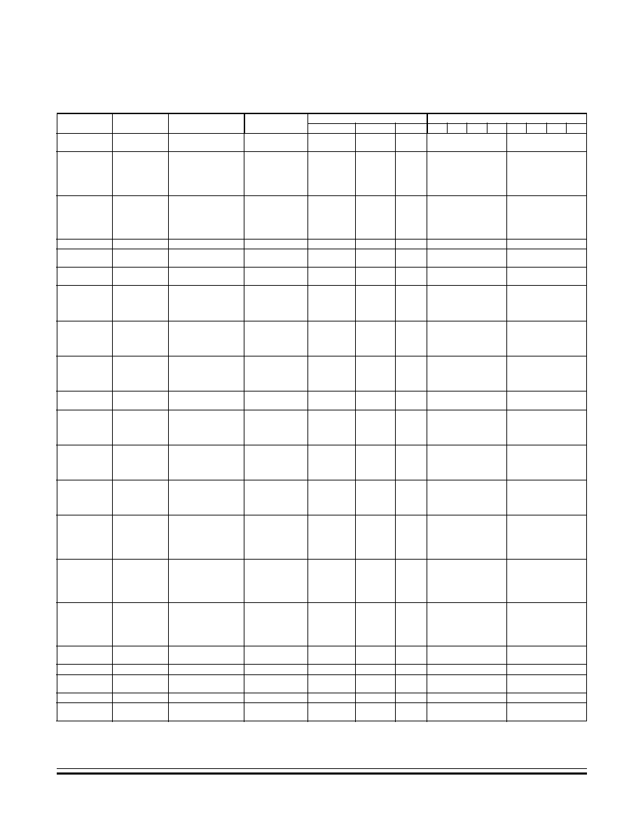
Central Processor Unit (CPU)
Instruction Set
M68HC11K Family
Technical Data
MOTOROLA
Central Processor Unit (CPU)
61
SBA
Subtract B from
A
A � B
A
INH
10
--
2
--
--
--
--
SBCA (opr)
Subtract with
Carry from A
A � M � C
A
A
IMM
A
DIR
A
EXT
A
IND,X
A
IND,Y
82
92
B2
A2
18
A2
ii
dd
hh ll
ff
ff
2
3
4
4
5
--
--
--
--
SBCB (opr)
Subtract with
Carry from B
B � M � C
B
B
IMM
B
DIR
B
EXT
B
IND,X
B
IND,Y
C2
D2
F2
E2
18
E2
ii
dd
hh ll
ff
ff
2
3
4
4
5
--
--
--
--
SEC
Set Carry
1
C
INH
0D
--
2
--
--
--
--
--
--
--
1
SEI
Set Interrupt
Mask
1
I
INH
0F
--
2
--
--
--
1
--
--
--
--
SEV
Set Overflow
Flag
1
V
INH
0B
--
2
--
--
--
--
--
--
1
--
STAA (opr)
Store
Accumulator
A
A
M
A
DIR
A
EXT
A
IND,X
A
IND,Y
97
B7
A7
18
A7
dd
hh ll
ff
ff
3
4
4
5
--
--
--
--
0
--
STAB (opr)
Store
Accumulator
B
B
M
B
DIR
B
EXT
B
IND,X
B
IND,Y
D7
F7
E7
18
E7
dd
hh ll
ff
ff
3
4
4
5
--
--
--
--
0
--
STD (opr)
Store
Accumulator
D
A
M, B
M + 1
DIR
EXT
IND,X
IND,Y
DD
FD
ED
18
ED
dd
hh ll
ff
ff
4
5
5
6
--
--
--
--
0
--
STOP
Stop Internal
Clocks
--
INH
CF
--
2
--
--
--
--
--
--
--
--
STS (opr)
Store Stack
Pointer
SP
M : M + 1
DIR
EXT
IND,X
IND,Y
9F
BF
AF
18
AF
dd
hh ll
ff
ff
4
5
5
6
--
--
--
--
0
--
STX (opr)
Store Index
Register X
IX
M : M + 1
DIR
EXT
IND,X
IND,Y
DF
FF
EF
CD
EF
dd
hh ll
ff
ff
4
5
5
6
--
--
--
--
0
--
STY (opr)
Store Index
Register Y
IY
M : M + 1
DIR
EXT
IND,X
IND,Y
18
DF
18
FF
1A
EF
18
EF
dd
hh ll
ff
ff
5
6
6
6
--
--
--
--
0
--
SUBA (opr)
Subtract
Memory from
A
A � M
A
A
IMM
A
DIR
A
EXT
A
IND,X
A
IND,Y
80
90
B0
A0
18
A0
ii
dd
hh ll
ff
ff
2
3
4
4
5
--
--
--
--
SUBB (opr)
Subtract
Memory from
B
B � M
B
A
IMM
A
DIR
A
EXT
A
IND,X
A
IND,Y
C0
D0
F0
E0
18
E0
ii
dd
hh ll
ff
ff
2
3
4
4
5
--
--
--
--
SUBD (opr)
Subtract
Memory from
D
D � M : M + 1
D
IMM
DIR
EXT
IND,X
IND,Y
83
93
B3
A3
18
A3
jj kk
dd
hh ll
ff
ff
4
5
6
6
7
--
--
--
--
SWI
Software
Interrupt
See
Figure 3-2
INH
3F
--
14
--
--
--
1
--
--
--
--
TAB
Transfer A to B
A
B
INH
16
--
2
--
--
--
--
0
--
TAP
Transfer A to
CC Register
A
CCR
INH
06
--
2
TBA
Transfer B to A
B
A
INH
17
--
2
--
--
--
--
0
--
TEST
TEST (Only in
Test Modes)
Address Bus Counts
INH
00
--
*
--
--
--
--
--
--
--
--
Table 3-1. Instruction Set (Sheet 6 of 7)
Mnemonic
Operation
Description
Addressing
Instruction
Condition Codes
Mode Opcode
Operand
Cycles
S
X
H
I
N
Z
V
C
Technical Data
M68HC11K Family
62
Central Processor Unit (CPU)
MOTOROLA
Central Processor Unit (CPU)
TPA
Transfer CC
Register to A
CCR
A
INH
07
--
2
--
--
--
--
--
--
--
--
TST (opr)
Test for Zero or
Minus
M � 0
EXT
IND,X
IND,Y
7D
6D
18
6D
hh ll
ff
ff
6
6
7
--
--
--
--
0
0
TSTA
Test A for Zero
or Minus
A � 0
A
INH
4D
--
2
--
--
--
--
0
0
TSTB
Test B for Zero
or Minus
B � 0
B
INH
5D
--
2
--
--
--
--
0
0
TSX
Transfer Stack
Pointer to X
SP + 1
IX
INH
30
--
3
--
--
--
--
--
--
--
--
TSY
Transfer Stack
Pointer to Y
SP + 1
IY
INH
18
30
--
4
--
--
--
--
--
--
--
--
TXS
Transfer X to
Stack Pointer
IX � 1
SP
INH
35
--
3
--
--
--
--
--
--
--
--
TYS
Transfer Y to
Stack Pointer
IY � 1
SP
INH
18
35
--
4
--
--
--
--
--
--
--
--
WAI
Wait for
Interrupt
Stack Regs & WAIT
INH
3E
--
**
--
--
--
--
--
--
--
--
XGDX
Exchange D
with X
IX
D, D
IX INH
8F
--
3
--
--
--
--
--
--
--
--
XGDY
Exchange D
with Y
IY
D, D
IY
INH
18
8F
--
4
--
--
--
--
--
--
--
--
Table 3-1. Instruction Set (Sheet 7 of 7)
Mnemonic
Operation
Description
Addressing
Instruction
Condition Codes
Mode Opcode
Operand
Cycles
S
X
H
I
N
Z
V
C
Cycle
*
Infinity or until reset occurs
**
12 cycles are used beginning with the opcode fetch. A wait state is entered which remains in effect for an integer number of MPU E-clock
cycles (n) until an interrupt is recognized. Finally, two additional cycles are used to fetch the appropriate interrupt vector (14 + n total).
Operands
dd
= 8-bit direct address ($0000�$00FF) (high byte assumed to be $00)
ff
= 8-bit positive offset $00 (0) to $FF (255) (is added to index)
hh
= High-order byte of 16-bit extended address
ii
= One byte of immediate data
jj
= High-order byte of 16-bit immediate data
kk
= Low-order byte of 16-bit immediate data
ll
= Low-order byte of 16-bit extended address
mm
= 8-bit mask (set bits to be affected)
rr
= Signed relative offset $80 (�128) to $7F (+127)
(offset relative to address following machine code offset byte))
Operators
( )
Contents of register shown inside parentheses
Is transferred to
Is pulled from stack
Is pushed onto stack
�
Boolean AND
+
Arithmetic addition symbol except where used as inclusive-OR symbol
in Boolean formula
Exclusive-OR
Multiply
:
Concatenation
�
Arithmetic subtraction symbol or negation symbol (two's complement)
Condition Codes
--
Bit not changed
0
Bit always cleared
1
Bit always set
Bit cleared or set, depending on operation
Bit can be cleared, cannot become set

M68HC11K Family
Technical Data
MOTOROLA
Operating Modes and On-Chip Memory
63
Technical Data -- M68HC11K Family
Section 4. Operating Modes and On-Chip Memory
4.1 Contents
4.2
Introduction . . . . . . . . . . . . . . . . . . . . . . . . . . . . . . . . . . . . . . . . 64
4.3
Control Registers . . . . . . . . . . . . . . . . . . . . . . . . . . . . . . . . . . . 64
4.4
System Initialization . . . . . . . . . . . . . . . . . . . . . . . . . . . . . . . . .76
4.5
Operating Modes . . . . . . . . . . . . . . . . . . . . . . . . . . . . . . . . . . . 77
4.5.1
Single-Chip Mode. . . . . . . . . . . . . . . . . . . . . . . . . . . . . . . . . 77
4.5.2
Expanded Mode . . . . . . . . . . . . . . . . . . . . . . . . . . . . . . . . . .77
4.5.3
Bootstrap Mode . . . . . . . . . . . . . . . . . . . . . . . . . . . . . . . . . . 78
4.5.4
Special Test Mode . . . . . . . . . . . . . . . . . . . . . . . . . . . . . . . . 79
4.5.5
Mode Selection. . . . . . . . . . . . . . . . . . . . . . . . . . . . . . . . . . . 79
4.6
Memory Map. . . . . . . . . . . . . . . . . . . . . . . . . . . . . . . . . . . . . . . 81
4.6.1
Control Registers and RAM . . . . . . . . . . . . . . . . . . . . . . . . . 84
4.6.2
ROM or EPROM. . . . . . . . . . . . . . . . . . . . . . . . . . . . . . . . . .87
4.6.3
EEPROM . . . . . . . . . . . . . . . . . . . . . . . . . . . . . . . . . . . . . . . 87
4.6.4
Bootloader ROM. . . . . . . . . . . . . . . . . . . . . . . . . . . . . . . . . .90
4.7
EPROM/OTPROM (M68HC711K4 and M68HC711KS2). . . . . 90
4.7.1
Programming the EPROM with Downloaded Data. . . . . . . . 90
4.7.2
Programming the EPROM from Memory . . . . . . . . . . . . . . .91
4.8
EEPROM and the CONFIG Register . . . . . . . . . . . . . . . . . . . . 93
4.8.1
EEPROM Registers . . . . . . . . . . . . . . . . . . . . . . . . . . . . . . . 94
4.8.1.1
EEPROM Programming Control Register . . . . . . . . . . . . 94
4.8.1.2
Block Protect Register . . . . . . . . . . . . . . . . . . . . . . . . . . . 96
4.8.1.3
System Configuration Options Register . . . . . . . . . . . . . . 97
4.8.2
EEPROM Programming . . . . . . . . . . . . . . . . . . . . . . . . . . . . 97
4.8.2.1
EEPROM Programming . . . . . . . . . . . . . . . . . . . . . . . . . . 98
4.8.2.2
EEPROM Bulk Erase . . . . . . . . . . . . . . . . . . . . . . . . . . . . 99
4.8.2.3
EEPROM Row Erase . . . . . . . . . . . . . . . . . . . . . . . . . . . . 99
4.8.2.4
EEPROM Byte Erase . . . . . . . . . . . . . . . . . . . . . . . . . . . . 99
4.8.3
CONFIG Register Programming . . . . . . . . . . . . . . . . . . . . 100
4.8.4
RAM and EEPROM Security . . . . . . . . . . . . . . . . . . . . . . .100
4.9
XOUT Pin Control . . . . . . . . . . . . . . . . . . . . . . . . . . . . . . . . . . 102
4.9.1
System Configuration Register. . . . . . . . . . . . . . . . . . . . . . 102
4.9.2
System Configuration Options 2 Register . . . . . . . . . . . . . 103

Technical Data
M68HC11K Family
64
Operating Modes and On-Chip Memory
MOTOROLA
Operating Modes and On-Chip Memory
4.2 Introduction
This section presents the elements involved in configuring the
M68HC11K/KS Family microcontrollers (MCUs), including:
�
A list of the control registers, see
4.3 Control Registers
�
Special registers that control system initialization, see
4.4 System
Initialization
�
Description of the four operating modes and how they're selected,
see
4.5 Operating Modes
�
Memory maps of the K Family, see
4.6 Memory Map
�
Information on programming EPROM (erasable, programmable
read-only memory) and EEPROM (electrically erasable,
programmable read-only memory), see
4.7 EPROM/OTPROM
(M68HC711K4 and M68HC711KS2)
and
4.8 EEPROM and the
CONFIG Register
4.3 Control Registers
The heart of the M68HC11 Family of MCUs is a special register block
which controls the peripheral functions. In the K Family, this block is 128
bytes. The default location of this block is the first 128 bytes of memory,
but software can map it to any 4-Kbyte boundary (see
4.6.1 Control
Registers and RAM
).
Certain bits and registers that control initialization and the basic
operation of the MCU are protected against writes in normal operating
modes except under special circumstances. Some bits cannot be written
at all; others can be written only once and/or within the first 64 bus cycles
after any reset. The special operating modes override these restrictions.
These bits and registers are discussed in
4.4 System Initialization
.
Normal and special operating modes are discussed in
4.5 Operating
Modes
. The write-restricted registers and bits are summarized in
Table 4-1
.
Figure 4-1
lists the entire 128-byte register block in ascending order by
address, using the default memory block assignment $0000�$007F.
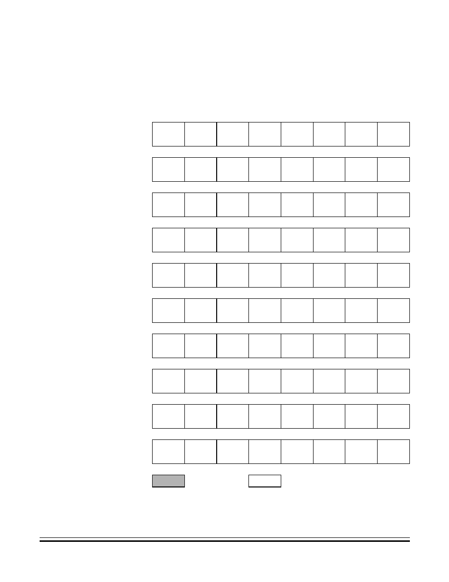
Operating Modes and On-Chip Memory
Control Registers
M68HC11K Family
Technical Data
MOTOROLA
Operating Modes and On-Chip Memory
65
NOTE:
Throughout this manual, the registers are discussed by function. In the
event that not all bits in a register are referenced, the bits that are not
discussed are shaded.
Addr.
Register Name
Bit 7
6
5
4
3
2
1
Bit 0
$0000
Port A Data Register
(PORTA)
See page 138.
Read:
PA7
PA6
PA5
PA4
PA3
PA2
PA1
PA0
Write:
Reset:
Undefined after reset
$0001
Port A Data Direction
Register (DDRA)
See page 138.
Read:
DDA7
DDA6
DDA5
DDA4
DDA3
DDA2
DDA1
DDA0
Write:
Reset:
0
0
0
0
0
0
0
0
$0002
Port B Data Direction
Register (DDRB)
See page 139.
Read:
DDB7
DDB6
DDB5
DDB4
DDB3
DDB2
DDB1
DDB0
Write:
Reset:
0
0
0
0
0
0
0
0
$0003
Port F Data Direction
Register (DDRF)
See page 144.
Read:
DDF7
DDF6
DDF5
DDF4
DDF3
DDF2
DDF1
DDF0
Write:
Reset:
0
0
0
0
0
0
0
0
$0004
Port B Data Register
(PORTB)
See page 139.
Read:
PB7
PB6
PB5
PB4
PB3
PB2
PB1
PB0
Write:
Reset:
Undefined after reset
$0005
Port F Data Register
(PORTF)
See page 144.
Read:
PF7
PF6
PF5
PF4
PF3
PF2
PF1
PF0
Write:
Reset:
Undefined after reset
$0006
Port C Data Register
(PORTC)
See page 140.
Read:
PC7
PC6
PC5
PC4
PC3
PC2
PC1
PC0
Write:
Reset:
Undefined after reset
$0007
Port C Data Direction
Register (DDRC)
See page 141.
Read:
DDC7
DDC6
DDC5
DDC4
DDC3
DDC2
DDC1
DDC0
Write:
Reset:
0
0
0
0
0
0
0
0
$0008
Port D Data Register
(PORTD)
See page 142.
Read:
0
0
PD5
PD4
PD3
PD2
PD1
PD0
Write:
Reset:
0
0
U
U
U
U
U
U
$0009
Port D Data Direction
Register (DDRD)
See page 142.
Read:
0
0
DDD5
DDD4
DDD3
DDD2
DDD1
DDD0
Write:
Reset:
0
0
0
0
0
0
0
0
= Unimplemented
R
= Reserved
U = Undefined
Figure 4-1. Register and Control Bit Assignments (Sheet 1 of 11)
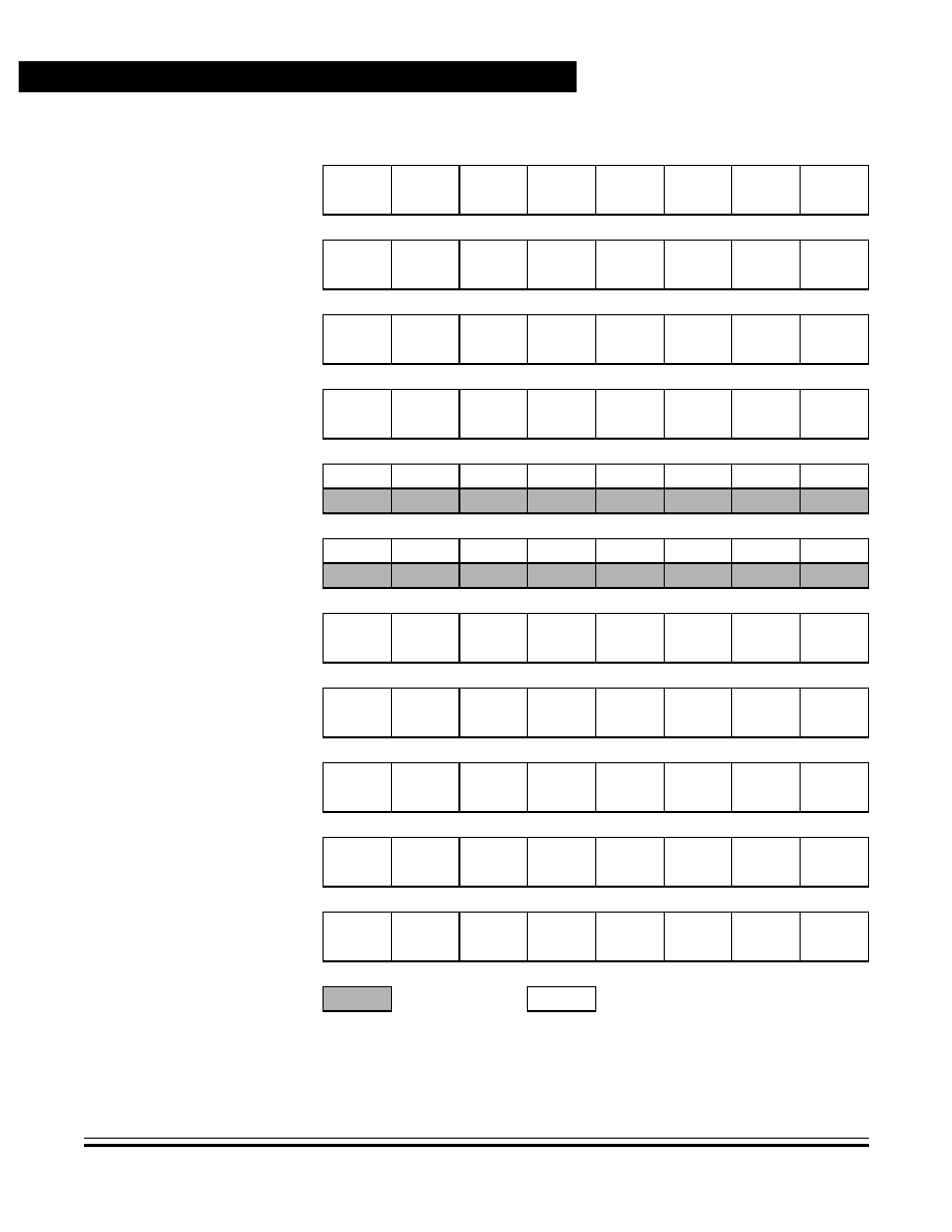
Technical Data
M68HC11K Family
66
Operating Modes and On-Chip Memory
MOTOROLA
Operating Modes and On-Chip Memory
$000A
Port E Data Register
(PORTE)
See page 143.
Read:
PE7
PE6
PE5
PE4
PE3
PE2
PD1
PD0
Write:
Reset:
Undefined after reset
$000B
Timer Compare Force
Register (CFORC)
See page 201.
Read:
FOC1
FOC2
FOC3
FOC4
FOC5
0
0
0
Write:
Reset:
0
0
0
0
0
0
0
0
$000C
Output Compare 1
Mask Register (OC1M)
See page 202.
Read:
OC1M7
OC1M6
OC1M5
OC1M4
OC1M3
0
0
0
Write:
Reset:
0
0
0
0
0
0
0
0
$000D
Output Compare 1 Data
Register (OC1D)
See page 202.
Read:
OC1D7
OC1D6
OC1D5
OC1D4
OC1D3
0
0
0
Write:
Reset:
0
0
0
0
0
0
0
0
$000E
Timer Counter Register
High (TCNTH)
See page 188.
Read:
Bit 15
Bit 14
Bit 13
Bit 12
Bit 11
Bit 10
Bit 9
Bit 8
Write:
Reset:
0
0
0
0
0
0
0
0
$000F
Timer Counter Register
Low (TCNTL)
See page 188.
Read:
Bit 7
Bit 6
Bit 5
Bit 4
Bit 3
Bit 2
Bit 1
Bit 0
Write:
Reset:
0
0
0
0
0
0
0
0
$0010
Timer Input Capture 1
Register High (TIC1H)
See page 192.
Read:
Bit 15
Bit 14
Bit 13
Bit 12
Bit 11
Bit 10
Bit 9
Bit 8
Write:
Reset:
Undefined after reset
$0011
Timer Input Capture 1
Register Low (TIC1L)
See page 192.
Read:
Bit 7
Bit 6
Bit 5
Bit 4
Bit 3
Bit 2
Bit 1
Bit 0
Write:
Reset:
Undefined after reset
$0012
Timer Input Capture 2
Register High (TIC2H)
See page 192.
Read:
Bit 15
Bit 14
Bit 13
Bit 12
Bit 11
Bit 10
Bit 9
Bit 8
Write:
Reset:
Undefined after reset
$0013
Timer Input Capture 2
Register Low (TIC2L)
See page 192.
Read:
Bit 7
Bit 6
Bit 5
Bit 4
Bit 3
Bit 2
Bit 1
Bit 0
Write:
Reset:
Undefined after reset
$0014
Timer Input Capture 3
Register High (TIC3H)
See page 192.
Read:
Bit 15
Bit 14
Bit 13
Bit 12
Bit 11
Bit 10
Bit 9
Bit 8
Write:
Reset:
Undefined after reset
Addr.
Register Name
Bit 7
6
5
4
3
2
1
Bit 0
= Unimplemented
R
= Reserved
U = Undefined
Figure 4-1. Register and Control Bit Assignments (Sheet 2 of 11)
Operating Modes and On-Chip Memory
Control Registers
M68HC11K Family
Technical Data
MOTOROLA
Operating Modes and On-Chip Memory
67
$0015
Timer Input Capture 3
Register Low (TIC3L)
See page 192.
Read:
Bit 7
Bit 6
Bit 5
Bit 4
Bit 3
Bit 2
Bit 1
Bit 0
Write:
Reset:
Undefined after reset
$0016
Timer Output
Compare 1 High
Register (TOC1H)
See page 197.
Read:
Bit 15
Bit 14
Bit 13
Bit 12
Bit 11
Bit 10
Bit 9
Bit 8
Write:
Reset:
1
1
1
1
1
1
1
1
$0017
Timer Output
Compare 1 Low
Register (TOC1L)
See page 197.
Read:
Bit 7
Bit 6
Bit 5
Bit 4
Bit 3
Bit 2
Bit 1
Bit 0
Write:
Reset:
1
1
1
1
1
1
1
1
$0018
Timer Output
Compare 2 High
Register (TOC2H)
See page 197.
Read:
Bit 15
Bit 14
Bit 13
Bit 12
Bit 11
Bit 10
Bit 9
Bit 8
Write:
Reset:
1
1
1
1
1
1
1
1
$0019
Timer Output
Compare 2 Low
Register (TOC2L)
See page 197.
Read:
Bit 7
Bit 6
Bit 5
Bit 4
Bit 3
Bit 2
Bit 1
Bit 0
Write:
Reset:
1
1
1
1
1
1
1
1
$001A
Timer Output
Compare 3 High
Register (TOC3H)
See page 197.
Read:
Bit 15
Bit 14
Bit 13
Bit 12
Bit 11
Bit 10
Bit 9
Bit 8
Write:
Reset:
1
1
1
1
1
1
1
1
$001B
Timer Output
Compare 3 Low
Register (TOC3L)
See page 197.
Read:
Bit 7
Bit 6
Bit 5
Bit 4
Bit 3
Bit 2
Bit 1
Bit 0
Write:
Reset:
1
1
1
1
1
1
1
1
$001C
Timer Output
Compare 4 High
Register (TOC4H)
See page 197.
Read:
Bit 15
Bit 14
Bit 13
Bit 12
Bit 11
Bit 10
Bit 9
Bit 8
Write:
Reset:
1
1
1
1
1
1
1
1
$001D
Timer Output
Compare 4 Low
Register (TOC4L)
See page 197.
Read:
Bit 7
Bit 6
Bit 5
Bit 4
Bit 3
Bit 2
Bit 1
Bit 0
Write:
Reset:
1
1
1
1
1
1
1
1
Addr.
Register Name
Bit 7
6
5
4
3
2
1
Bit 0
= Unimplemented
R
= Reserved
U = Undefined
Figure 4-1. Register and Control Bit Assignments (Sheet 3 of 11)
Technical Data
M68HC11K Family
68
Operating Modes and On-Chip Memory
MOTOROLA
Operating Modes and On-Chip Memory
$001E
Timer Input Capture 4/
Output Compare 5 Reg.
High (TI4H/O5H)
See page 199.
Read:
Bit 15
Bit 14
Bit 13
Bit 12
Bit 11
Bit 10
Bit 9
Bit 8
Write:
Reset:
1
1
1
1
1
1
1
1
$001F
Timer Input Capture 4/
Output Compare 5 Reg.
Low (TI4L/O5L)
See page 199.
Read:
Bit 7
Bit 6
Bit 5
Bit 4
Bit 3
Bit 2
Bit 1
Bit 0
Write:
Reset:
1
1
1
1
1
1
1
1
$0020
Timer Control 1
Register (TCTL1)
See page 200.
Read:
OM2
OL2
OM3
OL3
OM4
OL4
OM5
OL5
Write:
Reset:
0
0
0
0
0
0
0
0
$0021
Timer Control 2
Register (TCTL2)
See page 195.
Read:
EDG4B
EDG4A
EDG1B
EDG1A
EDG2B
EDG2A
EDG3B
EDG3A
Write:
Reset:
0
0
0
0
0
0
0
0
$0022
Timer Interrupt Mask 1
Register (TMSK1)
See page 200.
Read:
OC1I
OC2I
OC3I
OC4I
I4/O5I
IC1I
IC2I
IC3I
Write:
Reset:
0
0
0
0
0
0
0
0
$0023
Timer Interrupt Flag 1
Register (TFLG1)
See page 199.
Read:
OC1F
OC2F
OC3F
OC4F
I4/O5F
IC1F
IC2F
IC3F
Write:
Reset:
0
0
0
0
0
0
0
0
$0024
Timer Interrupt Mask 2
Register (TMSK2)
See page 209.
Read:
TOI
RTII
PAOVI
PAII
0
0
PR1
(1)
PR0
(1)
Write:
Reset:
0
0
0
0
0
0
0
0
1. Can be written only once in first 64 cycles out of reset in normal modes
$0025
Timer Interrupt Flag 2
(TFLG2)
See page 209.
Read:
TOF
RTIF
PAOVF
PAIF
0
0
0
0
Write:
Reset:
0
0
0
0
0
0
0
0
$0026
Pulse Accumulator
Control Register
(PACTL)
See page 210.
Read:
0
PAEN
PAMOD
PEDGE
0
I4/O5
RTR1
RTR0
Write:
Reset:
0
0
0
0
0
0
0
0
$0027
Pulse Accumulator
Count Register
(PACNT)
See page 208.
Read:
Bit 7
Bit 6
Bit 5
Bit 4
Bit 3
Bit 2
Bit 1
Bit 0
Write:
Reset:
Undefined after reset
Addr.
Register Name
Bit 7
6
5
4
3
2
1
Bit 0
= Unimplemented
R
= Reserved
U = Undefined
Figure 4-1. Register and Control Bit Assignments (Sheet 4 of 11)
Operating Modes and On-Chip Memory
Control Registers
M68HC11K Family
Technical Data
MOTOROLA
Operating Modes and On-Chip Memory
69
$0028
Serial Peripheral
Control Register
(SPCR)
See page 174.
Read:
SPIE
SPE
DWOM
MSTR
CPOL
CPHA
SPR1
SPR0
Write:
Reset:
0
0
0
0
0
1
U
U
$0029
Serial Peripheral Status
Register (SPSR)
See page 176.
Read:
SPIF
WCOL
0
MODF
0
0
0
0
Write:
Reset:
0
0
0
0
0
0
0
0
$002A
Serial Peripheral Data
Register (SPDR)
See page 177.
Read:
Bit 7
Bit 6
Bit 5
Bit 4
Bit 3
Bit 2
Bit 1
Bit 0
Write:
Reset:
Undefined after reset
$002B
EPROM Programming
Control Register
(EPROG)
(1)
See page 91.
Read:
R
0
ELAT
EXCOL
EXROW
0
0
EPGM
Write:
Reset:
0
0
0
0
0
0
0
0
1. Present only in EPROM (711) devices
$002C
Port Pullup Assignment
Register (PPAR)
See page 147.
Read:
0
0
0
0
HPPUE
GPPUE
FPPUE
BPPUE
Write:
Reset:
0
0
0
0
1
1
1
1
$002D
Port G Assignment
Register (PGAR)
See page 235.
Read:
0
0
PGAR5
PGAR4
PGAR3
PGAR2
PGAR1
PGAR0
Write:
Reset:
0
0
0
0
0
0
0
0
$002E
System Configuration
Options 3 Register
(OPT3)
(2)
See page 132.
Read:
SM
Write:
Reset:
0
0
0
0
0
0
0
0
2. Not available on M68HC11K4 devices
$002F
Reserved
R
R
R
R
R
R
R
R
$0030
Analog-to-Digital
Control/Status Register
(ADCTL)
See page 227.
Read:
CCF
0
SCAN
MULT
CD
CC
CB
CA
Write:
Reset:
0
0
U
U
U
U
U
U
$0031
Analog-to-Digital
Results Register 1
(ADR1)
See page 229.
Read:
Bit 7
Bit 6
Bit 5
Bit 4
Bit 3
Bit 2
Bit 1
Bit 0
Write:
Reset:
Undefined after reset
Addr.
Register Name
Bit 7
6
5
4
3
2
1
Bit 0
= Unimplemented
R
= Reserved
U = Undefined
Figure 4-1. Register and Control Bit Assignments (Sheet 5 of 11)
Technical Data
M68HC11K Family
70
Operating Modes and On-Chip Memory
MOTOROLA
Operating Modes and On-Chip Memory
$0032
Analog-to-Digital
Results Register 2
(ADR2)
See page 229.
Read:
Bit 7
Bit 6
Bit 5
Bit 4
Bit 3
Bit 2
Bit 1
Bit 0
Write:
Reset:
Undefined after reset
$0033
Analog-to-Digital
Results Register 3
(ADR3)
See page 229.
Read:
Bit 7
Bit 6
Bit 5
Bit 4
Bit 3
Bit 2
Bit 1
Bit 0
Write:
Reset:
Undefined after reset
$0034
Analog-to-Digital
Results Register 4
(ADR4)
See page 229.
l
Read:
Bit 7
Bit 6
Bit 5
Bit 4
Bit 3
Bit 2
Bit 1
Bit 0
Write:
Reset:
Undefined after reset
$0035
Block Protect Register
(BPROT)
(1)
See page 96.
Read:
BULKP
LVPEN
BPRT4
PTCON
BPRT3
BPRT2
BPRT1
BPRT0
Write:
Reset:
1
1
1
1
1
1
1
1
1. Can be written only once to 0 in first 64 cycles out of reset in normal modes
$0036
Reserved
R
R
R
R
R
R
R
R
$0037
EEPROM Mapping
Register (INIT2)
(2)
See page 89.
Read:
EE3
EE2
EE1
EE0
0
0
0
0
Write:
Reset:
0
0
0
0
0
0
0
0
2. Can only be written once after reset in normal modes
$0038
System Configuration
Options 2 Register
(OPT2)
See pages 40, 103,
112, 141,
Read:
LIRDV
CWOM
STRCH
(3)
IRVNE
(4)
LSBF
SPR2
XDV1
XDV0
Write:
Reset:
0
0
0
--
0
0
0
0
3. Not available on M68HC11KS devices
4. Can be written only once after reset in normal modes
$0039
System Configuration
Options Register
(OPTION)
See pages 97, 109,
111, 112, 121, 147
Read:
ADPU
CSEL
IRQE
(5)
DLY
(5)
CME
FCME
(5)
CR1
(5)
CR0
(5)
Write:
Reset:
0
0
0
1
0
0
0
0
5. Can only be written once in first 64 cycles out of reset in normal modes
Addr.
Register Name
Bit 7
6
5
4
3
2
1
Bit 0
= Unimplemented
R
= Reserved
U = Undefined
Figure 4-1. Register and Control Bit Assignments (Sheet 6 of 11)
Operating Modes and On-Chip Memory
Control Registers
M68HC11K Family
Technical Data
MOTOROLA
Operating Modes and On-Chip Memory
71
$003A
Arm/Reset COP Timer
Circuitry Register
(COPRST)
See page 110.
Read:
Bit 7
Bit 6
Bit 5
Bit 4
Bit 3
Bit 2
Bit 1
Bit 0
Write:
Reset:
0
0
0
0
0
0
0
0
$003B
EEPROM Programming
Control Register
(PPROG)
See page 91.
Read:
ODD
EVEN
LVPI
BYTE
ROW
ERASE
EELAT
EEPGM
Write:
Reset:
0
0
0
0
0
0
0
0
$003C
Highest Priority I-Bit
Interrupt and Misc.
Register (HPRIO)
See pages 80, 123
Read:
RBOOT
SMOD
MDA
PSEL4
PSEL3
PSEL2
PSEL1
PSEL0
Write:
Reset:
--
--
--
0
0
1
1
0
$003D
RAM and I/O Mapping
Register (INIT)
(1)
See page 84.
Read:
RAM3
RAM2
RAM1
RAM0
REG3
REG2
REG1
REG0
Write:
Reset:
0
0
0
0
0
0
0
0
1. Can only be written once in first 64 cycles out of reset in normal modes
$003E
Test 1 Register
(TEST1)
Read:
TILOP
0
OCCR
CBYP
DISR
FCM
FCOP
0
Write:
Reset:
0
0
0
0
0
0
0
0
$003F
System Configuration
Register (CONFIG)
See pages 88, 101,
108, 147
Read:
ROMAD
1
CLKX
PAREN
NOSEC
NOCOP
ROMON
EEON
Write:
Reset:
--
1
--
--
1
--
--
--
$0040
Reserved
R
R
R
R
R
R
R
R
to
$0055
Reserved
R
R
R
R
R
R
R
R
$0056
Memory Mapping Size
Register (MMSIZ)
(2)
See pages 235, 243
Read:
MXGS2
MXGS1
W2SZ1
W2SZ0
0
0
W1SZ1
W1SZ0
Write:
Reset:
0
0
0
0
0
0
0
0
$0057
Memory Mapping
Window Base Register
(MMWBR)
(2)
See page 236.
Read:
W2A15
W2A14
W2A13
0
W1A15
W1A14
W1A13
0
Write:
Reset:
0
0
0
0
0
0
0
0
2. Not available on M68HC11KS devices
Addr.
Register Name
Bit 7
6
5
4
3
2
1
Bit 0
= Unimplemented
R
= Reserved
U = Undefined
Figure 4-1. Register and Control Bit Assignments (Sheet 7 of 11)
Technical Data
M68HC11K Family
72
Operating Modes and On-Chip Memory
MOTOROLA
Operating Modes and On-Chip Memory
$0058
Memory Mapping
Window 1 Control
Register (MM1CR)
(1)
See page 237.
Read:
0
X1A18
X1A17
X1A16
X1A15
X1A14
X1A13
0
Write:
Reset:
0
0
0
0
0
0
0
0
$0059
Memory Mapping
Window 2 Control
Register (MM2CR)
(1)
See page 237.
Read:
0
X2A18
X2A17
X2A16
X2A15
X2A14
X2A13
0
Write:
Reset:
0
0
0
0
0
0
0
0
$005A
Chip Select Clock
Stretch Register
(CSCSTR)
(1)
See page 249.
Read:
IOSA
IOSB
GP1SA
GP1SB
GP2SA
GP2SB
PCSA
PCSB
Write:
Reset:
0
0
0
0
0
0
0
0
$005B
Chip Select Control
Register (CSCTL)
(1)
See pages 240, 241
Read:
IOEN
IOPL
IOCSA
IOSZ
GCSPR
PCSEN
PCSZA
PCSZB
Write:
Reset:
0
0
0
0
0
1
0
0
$005C
General-Purpose Chip
Select 1 Address
Register (GPCS1A)
(1)
See page 243.
Read:
G1A18
G1A17
G1A16
G1A15
G1A14
G1A13
G1A12
G1A11
Write:
Reset:
0
0
0
0
0
0
0
0
$005D
General-Purpose Chip
Select 1 Control
Register (GPCS1C)
(1)
See pages 244, 247
Read:
G1DG2
G1DPC
G1POL
G1AV
G1SZA
G1SZB
G1SZC
G1SZD
Write:
Reset:
0
0
0
0
0
0
0
0
$005E
General-Purpose Chip
Select 2 Address
Register (GPCS2A)
(1)
See page 245.
Read:
G2A18
G2A17
G2A16
G2A15
G2A14
G2A13
G2A12
G2A11
Write:
Reset:
0
0
0
0
0
0
0
0
$005F
General-Purpose Chip
Select 2 Control
Register (GPCS2C)
(1)
See pages 245, 247
Read:
0
G2DPC
G2POL
G2AV
G2SZA
G2SZB
G2SZC
G2SZD
Write:
Reset:
0
0
0
0
0
0
0
0
1. Not available on M68HC11KS devices
$0060
Pulse Width Modulation
Timer Clock Select
Register (PWCLK)
See page 213.
Read:
CON34
CON12
PCKA2
PCKA1
0
PCKB3
PCKB2
PCKB1
Write:
Reset:
0
0
0
0
0
0
0
0
$0061
Pulse Width Modulation
Timer Polarity Register
(PWPOL)
See page 215.
Read:
PCLK4
PCLK3
PCLK2
PCLK1
PPOL4
PPOL3
PPOL2
PPOL1
Write:
Reset:
0
0
0
0
0
0
0
0
Addr.
Register Name
Bit 7
6
5
4
3
2
1
Bit 0
= Unimplemented
R
= Reserved
U = Undefined
Figure 4-1. Register and Control Bit Assignments (Sheet 8 of 11)
Operating Modes and On-Chip Memory
Control Registers
M68HC11K Family
Technical Data
MOTOROLA
Operating Modes and On-Chip Memory
73
$0062
Pulse Width Modulation
Timer Prescaler
Register (PWSCAL)
See page 215.
Read:
Bit 7
Bit 6
Bit 5
Bit 4
Bit 3
Bit 2
Bit 1
Bit 0
Write:
Reset:
0
0
0
0
0
0
0
0
$0063
Pulse Width Modulation
Timer Enable Register
(PWEN)
See page 216.
Read:
TPWSL
DISCP
0
0
PWEN4
PWEN3
PWEN2
PWEN1
Write:
Reset:
0
0
0
0
0
0
0
0
$0064
Pulse Width Modulation
Timer Counter 1
Register (PWCNT1)
See page 217.
Read:
Bit 7
Bit 6
Bit 5
Bit 4
Bit 3
Bit 2
Bit 1
Bit 0
Write:
Reset:
0
0
0
0
0
0
0
0
$0065
Pulse Width Modulation
Timer Counter 2
Register (PWCNT2)
See page 217.
Read:
Bit 7
Bit 6
Bit 5
Bit 4
Bit 3
Bit 2
Bit 1
Bit 0
Write:
Reset:
0
0
0
0
0
0
0
0
$0066
Pulse Width Modulation
Timer Counter 3
Register (PWCNT3)
See page 217.
Read:
Bit 7
Bit 6
Bit 5
Bit 4
Bit 3
Bit 2
Bit 1
Bit 0
Write:
Reset:
0
0
0
0
0
0
0
0
$0067
Pulse Width Modulation
Timer Counter 4
Register (PWCNT4)
See page 217.
Read:
Bit 7
Bit 6
Bit 5
Bit 4
Bit 3
Bit 2
Bit 1
Bit 0
Write:
Reset:
0
0
0
0
0
0
0
0
$0068
Pulse Width Modulation
Timer Period 1 Register
(PWPER1)
See page 218.
Read:
Bit 7
Bit 6
Bit 5
Bit 4
Bit 3
Bit 2
Bit 1
Bit 0
Write:
Reset:
0
0
0
0
0
0
0
0
$0069
Pulse Width Modulation
Timer Period 2 Register
(PWPER2)
See page 218.
Read:
Bit 7
Bit 6
Bit 5
Bit 4
Bit 3
Bit 2
Bit 1
Bit 0
Write:
Reset:
0
0
0
0
0
0
0
0
$006A
Pulse Width Modulation
Timer Period 3 Register
(PWPER3)
See page 218.
Read:
Bit 7
Bit 6
Bit 5
Bit 4
Bit 3
Bit 2
Bit 1
Bit 0
Write:
Reset:
0
0
0
0
0
0
0
0
$006B
Pulse Width Modulation
Timer Period 4 Register
(PWPER4)
See page 218.
Read:
Bit 7
Bit 6
Bit 5
Bit 4
Bit 3
Bit 2
Bit 1
Bit 0
Write:
Reset:
0
0
0
0
0
0
0
0
Addr.
Register Name
Bit 7
6
5
4
3
2
1
Bit 0
= Unimplemented
R
= Reserved
U = Undefined
Figure 4-1. Register and Control Bit Assignments (Sheet 9 of 11)

Technical Data
M68HC11K Family
74
Operating Modes and On-Chip Memory
MOTOROLA
Operating Modes and On-Chip Memory
$006C
Pulse Width Modulation
Timer Duty Cycle 1
Register (PWDTY1)
See page 219.
Read:
Bit 7
Bit 6
Bit 5
Bit 4
Bit 3
Bit 2
Bit 1
Bit 0
Write:
Reset:
0
0
0
0
0
0
0
0
$006D
Pulse Width Modulation
Timer Duty Cycle 2
Register (PWDTY2)
See page 219.
Read:
Bit 7
Bit 6
Bit 5
Bit 4
Bit 3
Bit 2
Bit 1
Bit 0
Write:
Reset:
0
0
0
0
0
0
0
0
$006E
Pulse Width Modulation
Timer Duty Cycle 3
Register (PWDTY3)
See page 219.
Read:
Bit 7
Bit 6
Bit 5
Bit 4
Bit 3
Bit 2
Bit 1
Bit 0
Write:
Reset:
0
0
0
0
0
0
0
0
$006F
Pulse Width Modulation
Timer Duty Cycle 4
Register (PWDTY4)
See page 219.
Read:
Bit 7
Bit 6
Bit 5
Bit 4
Bit 3
Bit 2
Bit 1
Bit 0
Write:
Reset:
0
0
0
0
0
0
0
0
$0070
SCI Baud Rate Control
Register High (SCBDH)
See page 158.
Read:
BTST
BSPL
0
SBR12
SBR11
SBR10
SBR9
SBR8
Write:
Reset:
0
0
0
0
0
0
0
0
$0071
SCI Baud Rate Control
Register Low (SCBDL)
See page 158.
Read:
SBR7
SBR6
SBR5
SBR4
SBR3
SBR2
SBR1
SBR0
Write:
Reset:
0
0
0
0
0
1
0
0
$0072
SCI Control Register 1
(SCCR1)
See page 160.
Read:
LOOPS
WOMS
0
M
WAKE
ILT
PE
PT
Write:
Reset:
U
U
0
0
0
0
0
0
$0073
SCI Control Register 2
(SCCR2)
See page 161.
Read:
TIE
TCIE
RIE
ILIE
TE
RE
RWU
SBK
Write:
Reset:
0
0
0
0
0
0
0
0
$0074
SCI Status Register 1
(SCSR1)
See page 162.
Read:
TDRE
TC
RDRF
IDLE
OR
NF
FE
PF
Write:
Reset:
0
0
0
0
0
0
0
0
$0075
SCI Status Register 2
(SCSR2)
See page 164.
Read:
0
0
0
0
0
0
0
RAF
Write:
Reset:
1
1
0
0
0
0
0
0
$0076
SCI Data Register
(SCDR)
See page 165.
Read:
R8
T8
0
0
0
0
0
0
Write:
Reset:
Undefined after reset
Addr.
Register Name
Bit 7
6
5
4
3
2
1
Bit 0
= Unimplemented
R
= Reserved
U = Undefined
Figure 4-1. Register and Control Bit Assignments (Sheet 10 of 11)
Operating Modes and On-Chip Memory
Control Registers
M68HC11K Family
Technical Data
MOTOROLA
Operating Modes and On-Chip Memory
75
$0077
SCI Data Register
(SCDR)
See page 165.
Read:
R7/T7
R6/T6
R5/T5
R4/T4
R3/T3
R2/T2
R1/T1
R0/T0
Write:
Reset:
Undefined after reset
$0078
Reserved
R
R
R
R
R
R
R
R
to
$007B
Reserved
R
R
R
R
R
R
R
R
$007C
Port H Data Register
(PORTH)
See page 146.
Read:
PH7
(1)
PH6
(1)
PH5
(1)
PH4
(1)
PH3
PH2
PH1
PH0
Write:
Reset:
Undefined after reset
$007D
Port H Data Direction
Register (DDRH)
See page 146.
Read:
DDH7
(1)
DDH6
(1)
DDH5
(1)
DDH4
(1)
DDH3
DDH2
DDH1
DDH0
Write:
Reset:
0
0
0
0
0
0
0
0
$007E
Port G Data Register
(PORTG)
See page 145.
Read:
PG7
PG6
(1)
PG5
(1)
PG4
(1)
PG3
(1)
PG2
(1)
PG1
(1)
PG0
(1)
Write:
Reset:
Undefined after reset
$007F
Port G Data Direction
Register (DDRG)
See page 145.
Read:
DDG7
DDG6
(1)
DDG5
(1)
DDG4
(1)
DDG3
(1)
DDG2
(1)
DDG1
(1)
DDG0
(1)
Write:
Reset:
0
0
0
0
0
0
0
0
1. Not available on M68HC11KS devices
Addr.
Register Name
Bit 7
6
5
4
3
2
1
Bit 0
= Unimplemented
R
= Reserved
U = Undefined
Figure 4-1. Register and Control Bit Assignments (Sheet 11 of 11)
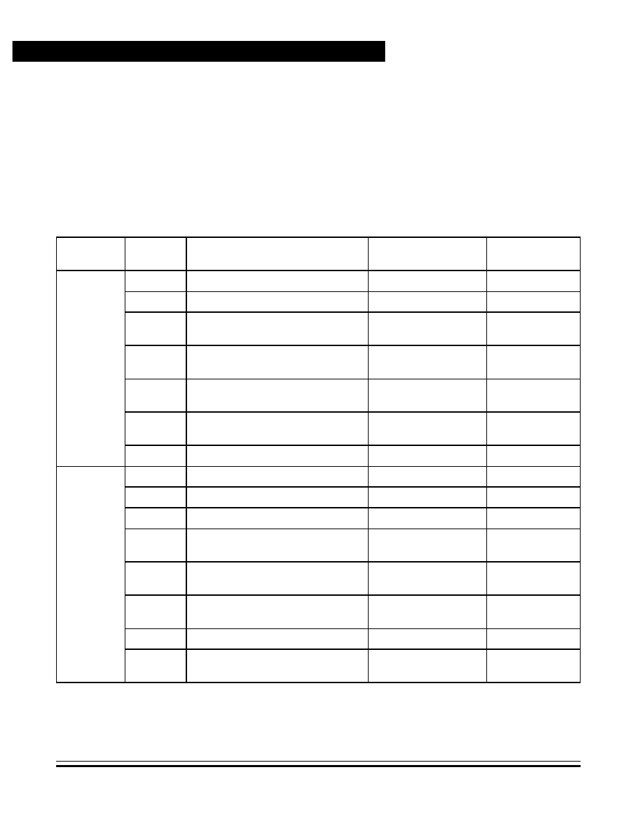
Technical Data
M68HC11K Family
76
Operating Modes and On-Chip Memory
MOTOROLA
Operating Modes and On-Chip Memory
4.4 System Initialization
Registers and bits that control initialization and the basic operation of the
MCU are protected against writes except under special circumstances.
Table 4-1
lists registers that can be written only once after reset or that
must be written within the first 64 cycles after reset.
Table 4-1. Registers with Limited Write Access
Operating
Mode
Register
Address
Register Name
Must be Written
in First 64 Cycles
Write
Anytime
SMOD = 0
$x024
Timer interrupt mask 2 (TMSK2)
Bits [1:0], once only
Bits [7:2]
$x035
Block protect register (BPROT)
Clear bits, once only
Set bits only
$x037
EEPROM mapping register (INIT2)
No, bits [7:4], once
only
--
$x038
System configuration options 2
register (OPT2)
No, bit 4, once only
See OPT2
description
$x039
System configuration
options (OPTION)
Bits [5:4], bits [2:0],
once only
Bits [7:6], bit 3
$x03C
Highest priority I-bit interrupt
and miscellaneous (HPRIO)
--
See HPRIO
description
$x03D
RAM and I/O map register (INIT)
Yes, once only
--
SMOD = 1
$x024
Timer interrupt mask 2 (TMSK2)
--
All, set or clear
$x035
Block protect register (BPROT)
--
All, set or clear
$x037
EEPROM mapping register (INIT2)
--
Bits [7:4]
$x038
System configuration options 2
register (OPT2)
--
See OPT2
description
$x039
System configuration options
(OPTION)
--
All, set or clear
$x03C
Highest priority I-bit interrupt and
miscellaneous (HPRIO)
--
See HPRIO
description
$x03D
RAM and I/O map register (INIT)
--
All, set or clear
$x03F
System configuration register
(CONFIG)
--
See CONFIG
description

Operating Modes and On-Chip Memory
Operating Modes
M68HC11K Family
Technical Data
MOTOROLA
Operating Modes and On-Chip Memory
77
4.5 Operating Modes
The two normal modes of operation in the M68HC11K Family are:
�
Single-chip mode -- All port pins available for input/output (I/O);
only on-board memory accessible
�
Expanded mode -- Access to internal and external memory; 25
I/O pins used for interface
The two special modes of operation are:
�
Bootstrap mode -- A variation of single-chip mode; executes a
bootloader program in an internal bootstrap read-only memory
(ROM)
�
Test mode -- A variation of the expanded mode used in
production testing; allows privileged access to internal resources
The logic levels applied at reset to input pins MODA and MODB
determine the operating mode. See
4.5.5 Mode Selection
.
4.5.1 Single-Chip Mode
In single-chip mode, the MCU functions as a self-contained
microcontroller. In this mode, all address and data activity occurs within
the MCU. Ports B, C, F, G, and H are available for general-purpose I/O
because the external address and data buses are not required.
4.5.2 Expanded Mode
In expanded mode, the MCU uses ports B, C, F, and G to access a
64-Kbyte address space. This includes:
�
The same on-chip memory addresses used in single-chip mode
�
External memory
�
Peripheral devices

Technical Data
M68HC11K Family
78
Operating Modes and On-Chip Memory
MOTOROLA
Operating Modes and On-Chip Memory
Port B provides the high-order address byte (Addr[15:8]), port F the
low-order address byte (Addr[7:0]), port C the data bus (Data[7:0]), and
port G pin 7 the read/write line (R/W) which controls direction of data
flow.
Additionally, the E clock output can be used to synchronize external
decoders for enable signals.
Expanded mode also enables these two special features available only
on the K4 Family devices:
1. Memory expansion uses port G[5:0] to increase the available
external address space to 1 Mbyte.
2. Four chip-select lines on port H[7:4] simplify selection of external
memory devices.
Both of these features are described in
Section 11. Memory Expansion
and Chip Selects
.
4.5.3 Bootstrap Mode
Resetting the MCU in special bootstrap mode selects a reset vector to a
special ROM bootloader program at addresses $BE00�$BFFF. The
bootloader program is used to download code, such as programming
algorithms, into on-chip RAM through the SCI. To do this:
1. Send a synchronization character (see
Table 4-2
) to the SCI
receiver at the specified baud rate.
2. Download up to 768 bytes (1 Kbyte for KS2) of program data,
which the CPU places into RAM starting at $0080 and also echoes
back on the TxD signal. The bootloader program ends the
download after the RAM is full or when the received data line is
idle for at least four character times. See
Table 4-2
.
When loading is complete, the MCU jumps to location $0080 and begins
executing the code. Interrupt vectors are directed to RAM, which allows
the use of interrupts through a jump table. The SCI transmitter requires
an external pullup resistor since it is part of port D, which the bootloader
configures for wired-OR operation.
Operating Modes and On-Chip Memory
Operating Modes
M68HC11K Family
Technical Data
MOTOROLA
Operating Modes and On-Chip Memory
79
For a detailed description of bootstrap mode, refer to the Motorola
application note entitled MC68HC11 Bootstrap Mode, document order
number AN1060/D.
4.5.4 Special Test Mode
Special test mode, a variation of the expanded mode, is used primarily
during Motorola's internal production testing. However, for those devices
containing EPROM, it can be used to program the EPROM for program
calibration data in EEPROM and support emulation and debugging
during development.
For more detailed information, refer to
4.7.1 Programming the EPROM
with Downloaded Data
.
4.5.5 Mode Selection
The operating mode is selected by applying the appropriate logic states
to the MODA and MODB pins during reset. MODA selects single-chip
mode (0) or expanded mode (1). A logic high on MODB selects normal
modes, and vectors are fetched from memory area $FFC0�$FFFF. A
logic low on MODB selects special modes, and reset vectors are fetched
from memory area $BFC0�$BFFF. Values reflecting the selected mode
are latched into the RBOOT, SMOD, and MDA bits of the highest priority
I-bit interrupt and miscellaneous register (HPRIO) on the rising edge of
RESET.
Table 4-2. Synchronization Character Selection
Synchronization
Character
Timeout
Delay
Baud Rate at E Clocks
2 MHz
3 MHz
4 MHz
$FF
4 characters
7812
11,718
15,624
$FF
4 characters
1200
1800
2400
$F0
4.9 characters
9600
14,400
19,200
$FD
13 characters
3906
5859
7812
Technical Data
M68HC11K Family
80
Operating Modes and On-Chip Memory
MOTOROLA
Operating Modes and On-Chip Memory
Table 4-3
summarizes the inputs, modes selected, and register bits
latched. The HPRIO register is illustrated in
Figure 4-2
.
RBOOT -- Read Bootstrap ROM Bit
In special modes, this bit enables the bootloader ROM
0 = Bootloader ROM disabled and not in map
1 = Bootloader ROM enabled and located in map at $BE00�$BFFF
In normal modes this bit is clear and cannot be written.
SMOD -- Special Mode Select Bit
This bit reflects the inverse of the MODB input pin at the rising edge
of RESET. If MODB is low during reset, SMOD is set; if MODB is high
during reset, SMOD is cleared. Software can clear the SMOD bit, but
cannot set it. Thus, it is possible for software to change the operating
Table 4-3. Hardware Mode Select Summary
Inputs
Mode
Control Bits in HPRIO
Latched at Reset
MODB
MODA
RBOOT
SMOD
MDA
1
0
Single-chip
0
0
0
1
1
Expanded
0
0
1
0
0
Special bootstrap
1
1
0
0
1
Special test
0
1
1
Address: $003C
Bit 7
6
5
4
3
2
1
Bit 0
Read:
RBOOT
(1)
SMOD
(1)
MDA
(1)
PSEL4
PSEL3
PSEL2
PSEL1
PSEL0
Write:
Reset:
--
--
--
0
0
1
1
0
1. The values of the RBOOT, SMOD, and MDA bits at reset depend on the mode during
initialization.
Figure 4-2. Highest Priority I-Bit Interrupt
and Miscellaneous Register (HPRIO)

Operating Modes and On-Chip Memory
Memory Map
M68HC11K Family
Technical Data
MOTOROLA
Operating Modes and On-Chip Memory
81
mode from special to normal, but not vice versa. To switch from a
special mode to a normal mode, write to the access-limited registers
(see
Table 4-1
) before clearing SMOD.
0 = Normal mode operation in effect
1 = Special mode operation in effect
MDA -- Mode Select A Bit
The mode select A bit reflects the status of the MODA input pin at the
rising edge of RESET. Software can change the MDA bit only while
the SMOD bit is set, effectively switching the operating mode between
special bootstrap and special test modes. Once the SMOD bit is clear,
the MODA bit is read-only and the operating mode cannot be changed
without going through a reset sequence.
0 = Normal single-chip or special bootstrap mode in effect
1 = Normal expanded or special test mode in effect
After RESET is released, the mode select pins revert to their alternate
functions, described in
2.9 Mode Selection, Instruction Cycle
Reference, and Standby Power (MODA/LIR and MODB/VSTBY)
, and
no longer influence the MCU operating mode.
4.6 Memory Map
The operating mode determines memory mapping and whether memory
is addressed on-chip or off-chip.
Figure 4-3
and
Figure 4-4
illustrate the
M68HC11K4 Family and M68HC11KS Family memory maps for each of
the four modes of operation. Memory locations for on-chip resources are
the same for both expanded and single-chip modes.
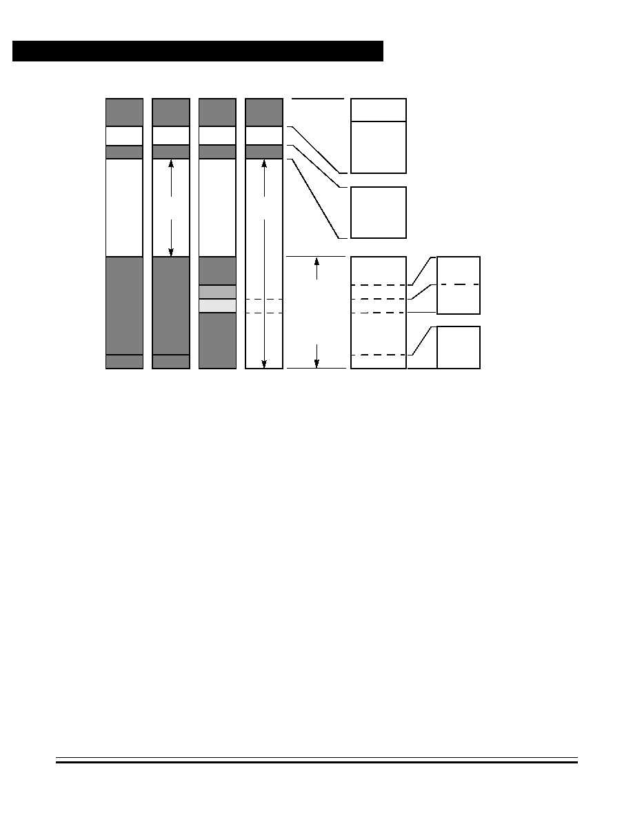
Technical Data
M68HC11K Family
82
Operating Modes and On-Chip Memory
MOTOROLA
Operating Modes and On-Chip Memory
Figure 4-3. M68HC11K4 Family Memory Map
$0380
$1000
$0D80
$A000
$FFC0
$FFFF
EXTERNAL
0000
007F
0080
037F
0D80
0FFF
A000
FFFF
EXTERNAL
EXTERNAL
BE00
BFC0
BFFF
FFC0
FFFF
SINGLE
CHIP
EXPANDED BOOTSTRAP
SPECIAL
TEST
EXTERNAL
Note 1.EPROM can be enabled in special test mode by setting the ROMON bit in the CONFIG register after reset.
128-BYTE REGISTER BLOCK
(CAN BE REMAPPED TO ANY 4-KBYTE
BOUNDARY BY THE INIT REGISTER)
768 BYTES RAM
(CAN BE REMAPPED TO ANY 4-KBYTE
BOUNDARY BY THE INIT REGISTER)
640 BYTES EEPROM
(CAN BE REMAPPED TO ANY 4-KBYTE
BOUNDARY BY THE INIT2 REGISTER)
BOOT ROM
(ONLY PRESENT IN
SPECIAL BOOT MODE)
SPECIAL MODES
INTERRUPT
VECTORS
NORMAL MODES
INTERRUPT
VECTORS
24-KBYTE ROM/
EPROM
(CAN BE
RE-MAPPED TO
$2000�$7FFF
BY THE CONFIG
REGISTER)
(1),(2)
$0000
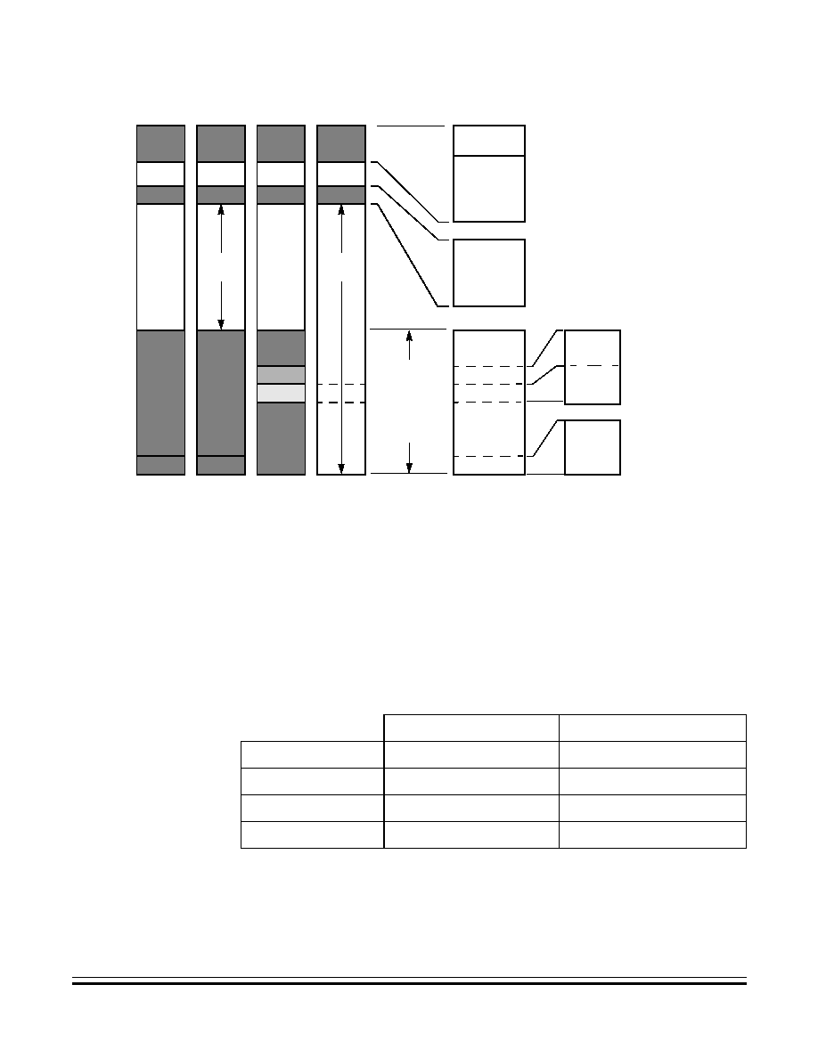
Operating Modes and On-Chip Memory
Memory Map
M68HC11K Family
Technical Data
MOTOROLA
Operating Modes and On-Chip Memory
83
Figure 4-4. M68HC11KS2 Family Memory Map
Table 4-4
shows the default memory map addresses for the M68HC11K
Family devices.
$0480
$1000
$0D80
$8000
$FFC0
$FFFF
EXTERNAL
0000
007F
0080
047F
0D80
0FFF
8000
FFFF
EXTERNAL
EXTERNAL
BE00
BFC0
BFFF
FFC0
FFFF
SINGLE-
CHIP
EXPANDED BOOTSTRAP
SPECIAL
TEST
EXTERNAL
Note: 1.EPROM can be enabled in special test mode by setting the ROMON bit in the CONFIG register after reset.
128-BYTE REGISTER BLOCK
(CAN BE REMAPPED TO ANY 4K
BOUNDARY BY THE INIT REGISTER)
1.0-KBYTE RAM
(CAN BE REMAPPED TO ANY 4-KBYTE
BOUNDARY BY THE INIT REGISTER)
640-BYTE EEPROM
(CAN BE REMAPPED TO ANY 4-KBYTE
BOUNDARY BY THE INIT2 REGISTER)
BOOT ROM
(ONLY PRESENT IN
SPECIAL BOOT MODE)
SPECIAL MODES
INTERRUPT
VECTORS
NORMAL MODES
INTERRUPT
VECTORS
32K ROM/
EPROM
(CAN BE
RE-MAPPED TO
$0000�$7FFF
BY THE CONFIG
REGISTER)
(1),(2)
$0000
Table 4-4. Default Memory Map Addresses
[7]11K4
[7]11KS2
Registers
$0000�$007F
$0000�$007F
RAM
$0080�$037F
$0080�$047F
EEPROM
$0D80�$0FFF
$0D80�$0FFF
ROM/EPROM
$A000�$FFFF
$8000�$FFFF

Technical Data
M68HC11K Family
84
Operating Modes and On-Chip Memory
MOTOROLA
Operating Modes and On-Chip Memory
4.6.1 Control Registers and RAM
Out of reset, the 128-byte register block is mapped to $0000 and the
768-byte RAM (1 Kbyte on the [7]11KS2) is mapped to $0080. Both the
register block and the RAM can be placed at any other 4-Kbyte boundary
($x000 and $x080, respectively) by writing the appropriate value to the
INIT register.
NOTE:
INIT is writable once in normal modes and writable at any time in special
modes.
RAM[3:0] -- RAM Map Position Bits
These four bits determine the position of RAM in the memory map by
specifying the upper hexadecimal digit of the RAM address. Refer to
Table 4-5
.
REG[3:0] -- Register Block Position Bits
These four bits determine the position of the register block in memory
by specifying the upper hexadecimal digit of the block address. Refer
to
Table 4-6
.
Address: $003D
Bit 7
6
5
4
3
2
1
Bit 0
Read:
RAM3
RAM2
RAM1
RAM0
REG3
REG2
REG1
REG0
Write:
Reset:
0
0
0
0
0
0
0
0
Figure 4-5. RAM and I/O Mapping Register (INIT)
Operating Modes and On-Chip Memory
Memory Map
M68HC11K Family
Technical Data
MOTOROLA
Operating Modes and On-Chip Memory
85
Table 4-5. RAM Mapping
RAM[3:0]
Address
(1)
1. RAM[3:0] = REG[3:0]: On the [7]11KS2, RAM address range is $x080�$x47F.
Address
(2)
2. RAM[3:0]
REG[3:0]: On the [7]11KS2, RAM address range is $x000�$x37F.
0000
$0080�$037F
(3)
3. Default locations out of reset
$0000�$02FF
0001
$1080�$137F
$1000�$12FF
0010
$2080�$237F
$2000�$22FF
0011
$3080�$337F
$3000�$32FF
0100
$4080�$437F
$4000�$42FF
0101
$5080�$537F
$5000�$52FF
0110
$6080�$637F
$6000�$62FF
0111
$7080�$737F
$7000�$72FF
1000
$8080�$837F
$8000�$82FF
1001
$9080�$937F
$9000�$92FF
1010
$A080�$A37F
$A000�$A2FF
1011
$B080�$B37F
$B000�$B2FF
1100
$C080�$C37F
$C000�$C2FF
1101
$D080�$D37F
$D000�$D2FF
1110
$E080�$E37F
$E000�$E2FF
1111
$F080�$F37F
$F000�$F2FF

Technical Data
M68HC11K Family
86
Operating Modes and On-Chip Memory
MOTOROLA
Operating Modes and On-Chip Memory
Since the direct addressing mode accesses RAM more quickly and
efficiently than other addressing modes, many applications will find the
default locations of registers and on-board RAM at the bottom of
memory to be the most advantageous.
When RAM and the registers are both mapped to different 4-K
boundaries, the registers are mapped at $x000�$x07F, and RAM is
moved to $x000�$x2FF ($x000�x3FF for the [7]11KS2).
Table 4-6. Register Mapping
REG[3:0]
Address
0000
$0000�$007F
(1)
1. Default locations out of reset.
0001
$1000�$107F
0010
$2000�$207F
0011
$3000�$307F
0100
$4000�$407F
0101
$5000�$507F
0110
$6000�$607F
0111
$7000�$707F
1000
$8000�$807F
1001
$9000�$907F
1010
$A000�$A07F
1011
$B000�$B07F
1100
$C000�$C07F
1101
$D000�$D07F
1110
$E000�$E07F
1111
$F000�$F07F

Operating Modes and On-Chip Memory
Memory Map
M68HC11K Family
Technical Data
MOTOROLA
Operating Modes and On-Chip Memory
87
4.6.2 ROM or EPROM
The presence and location of the 24-Kbyte (EP)ROM on the [7]11K4 is
determined by two bits in the system configuration register (CONFIG).
The CONFIG register is a special EEPROM register (see
Figure 4-6
).
(EP)ROM is present in the memory map when the ROMON bit is set and
removed from the memory map when the bit is cleared. The default
location of this memory is $A000�$FFFF, but it can be moved to
$2000�$7FFF in expanded mode by clearing the ROMAD bit. Both bits
are set out of reset in single-chip mode.
�
On the [7]11KS2, (EP)ROM is 32 K, mapped to $8000�$FFFF by
default, and moved to $0000�$7FFF by clearing the ROMAD bit.
In special test mode, the ROMON bit is forced to 0, removing (EP)ROM
from the memory map.
4.6.3 EEPROM
The M68HC11K Family devices contain 640 bytes of EEPROM. It is
initially located at $0D80 after reset if it is enabled by the EEON bit in the
CONFIG register (see
Figure 4-6
). It can be relocated to any 4-K
boundary ($xD80) by writing to the EEPROM mapping register (INIT2)
(see
Figure 4-7
).
NOTE:
On the M68HC11K devices, the EEPROM can be mapped to where it
will contain the vector space.

Technical Data
M68HC11K Family
88
Operating Modes and On-Chip Memory
MOTOROLA
Operating Modes and On-Chip Memory
NOTE:
CONFIG is writable once in normal modes and writable at any time in
special modes.
ROMAD -- ROM Address Mapping Control Bit
Set out of reset in single-chip mode
0 = (EP)ROM set at $2000�$7FFF;
$0000�$7FFF in [7]11KS2;
$0000�$BFFF in [7]11KS8
(expanded mode only)
1 = (EP)ROM set at $A000�$FFFF;
$8000�$FFFF in [7]11KS2;
$4000�$FFFF in [7]11KS8
ROMON -- ROM/PROM Enable Bit
Set by reset in single-chip mode; cleared by reset in special test mode
0 = (EP)ROM removed from the memory map
1 = (EP)ROM present in the memory map
EEON -- EEPROM Enable Bit
0 = 640-byte EEPROM disabled
1 = 640-byte EEPROM enabled
Address: $003F
Bit 7
6
5
4
3
2
1
Bit 0
Read:
ROMAD
1
CLKX
PAREN
NOSEC
NOCOP
ROMON
EEON
Write:
Reset:
--
1
--
--
--
--
--
--
Figure 4-6. System Configuration Register (CONFIG)
Operating Modes and On-Chip Memory
Memory Map
M68HC11K Family
Technical Data
MOTOROLA
Operating Modes and On-Chip Memory
89
NOTE:
INIT2 is writable once in normal modes and writable at any time in
special modes.
EE[3:0] -- EEPROM Map Position Bits
These four bits determine the most-significant hexadecimal digit in
the address range of the EEPROM, as shown in
Table 4-7
.
Address: $0037
Bit 7
6
5
4
3
2
1
Bit 0
Read:
EE3
EE2
EE1
EE0
0
0
0
0
Write:
Reset:
0
0
0
0
0
0
0
0
Figure 4-7. EEPROM Mapping Register (INIT2)
Table 4-7. EEPROM Map
EE[3:0]
Location
0000
$0D80�$0FFF
0001
$1D80�$1FFF
0010
$2D80�$2FFF
0011
$3D80�$3FFF
0100
$4D80�$4FFF
0101
$5D80�$5FFF
0110
$6D80�$6FFF
0111
$7D80�$7FFF
1000
$8D80�$8FFF
1001
$9D80�$9FFF
1010
$AD80�$AFFF
1011
$BD80�$BFFF
1100
$CD80�$CFFF
1101
$DD80�$DFFF
1110
$ED80�$EFFF
1111
$FD80�$FFFF

Technical Data
M68HC11K Family
90
Operating Modes and On-Chip Memory
MOTOROLA
Operating Modes and On-Chip Memory
4.6.4 Bootloader ROM
The bootloader program occupies 512 bytes of bootstrap ROM at
addresses $BE00�$BFFF. It is active only in special modes when the
RBOOT bit in the HPRIO register is set.
4.7 EPROM/OTPROM (M68HC711K4 and M68HC711KS2)
The M68HC711K4 devices include 24 Kbytes of on-chip EPROM
(OTPROM in non-windowed packages). The M68HC711KS2 has
32 Kbytes of EPROM.
The two methods available to program the EPROM are:
�
Downloading data through the serial communication interface
(SCI) in bootstrap or special test mode
�
Programming individual bytes from memory
Before proceeding with programming:
�
Ensure that the CONFIG register ROMON bit is set.
�
Ensure that the IRQ pin is pulled to a high level.
�
Apply 12 volts to the XIRQ/V
PP
pin.
Program the EPROM only at room temperature. Place an opaque label
over the quartz window on windowed parts after programming.
4.7.1 Programming the EPROM with Downloaded Data
The MCU can download EPROM data through the SCI while in the
special test or bootstrap modes. This can be done either with custom
software, also downloaded through the SCI, or with a built-in utility
program in bootstrap ROM. In either case, the 12-volt nominal
programming voltage must be present on the XIRQ/V
PP
pin.
To use the bootstrap ROM utility, download a 3-byte program consisting
of a single jump instruction to $BF00, the starting address of the resident
EPROM programming utility. The utility program sets the X and Y index
Operating Modes and On-Chip Memory
EPROM/OTPROM (M68HC711K4 and M68HC711KS2)
M68HC11K Family
Technical Data
MOTOROLA
Operating Modes and On-Chip Memory
91
registers to default values, then receives data from an external host and
programs it into the EPROM. The value in the X index register
determines programming delay time. The value in the Y index register is
a pointer to the first address in EPROM to be programmed. The default
starting address is $8000 for the M68HC11KS2.
When the utility program is ready to receive programming data, it sends
the host a $FF character and waits for a reply. When the host sees the
$FF character, it sends the EPROM programming data, starting with the
first location in the EPROM array. After the MCU receives the last byte
to be programmed and returns the corresponding verification data, it
terminates the programming operation by initiating a reset. Refer to the
Motorola application note entitled MC68HC11 Bootstrap Mode,
document order number AN1060/D.
4.7.2 Programming the EPROM from Memory
In this method, software programs the EPROM one byte at a time. Each
byte is read from memory, then latched and programmed into the
EPROM using the EPROM programming control register (EPROG). This
procedure can be done in any operating mode.
MBE -- Multiple-Byte Program Enable Bit
MBE is for factory use only and is accessible only in special test
mode. When MBE is set, the MCU ignores address bit 5, so that bytes
with ADDR5 = 0 and ADDR5 = 1 both get programmed with the same
data.
0 = Normal programming
1 = Multiple-byte programming enabled
Address: $002B
Bit 7
6
5
4
3
2
1
Bit 0
Read:
R
0
ELAT
EXCOL
EXROW
0
0
EPGM
Write:
Reset:
0
0
0
0
0
0
0
0
R
= Reserved
Figure 4-8. EPROM Programming Control Register (EPROG)

Technical Data
M68HC11K Family
92
Operating Modes and On-Chip Memory
MOTOROLA
Operating Modes and On-Chip Memory
ELAT -- EPROM Latch Control Bit
Setting ELAT latches the address and data of writes to the EPROM.
The EPROM cannot be read. ELAT can be read at any time. ELAT
can be written any time except when PGM = 1, which disables writes
to ELAT.
0 = EPROM address and data bus configured for normal reads.
EPROM cannot be programmed.
1 = EPROM address and data bus are configured for
programming. Address and data of writes to EPROM are
latched. EPROM cannot be read.
EXCOL -- Select Extra Columns Bit
EXCOL is for factory use only and is accessible only in special test
mode. When EXCOL equals 1, extra columns can be accessed at
bit 7 and bit 0. Addresses use bits [11:5]. Bits [4:1] are ignored.
0 = User array selected
1 = Extra columns selected and user array disabled
EXROW -- Select Extra Rows Bit
EXROW is for factory use only and is only accessible in special test
mode. When EXROW equals 1, two extra rows are available.
Addresses use bits [5:0]. Bits [11:6] are ignored.
0 = User array selected
1 = Extra rows selected and user array is disabled
EPGM -- EPROM Programming Enable Bit
EPGM applies programming voltage (V
PP
) to the EPROM. EPGM can
be read at any time. EPGM can be written only when ELAT = 1.
0 = Programming voltage to EPROM array is disconnected
1 = Programming voltage to EPROM array is connected; ELAT
cannot be changed.

Operating Modes and On-Chip Memory
EEPROM and the CONFIG Register
M68HC11K Family
Technical Data
MOTOROLA
Operating Modes and On-Chip Memory
93
This procedure programs one byte into EPROM. On entry, accumulator
A contains the byte of data to be programmed and X contains the target
EPROM address.
EPROG LDAB
#$20
STAB
$002B
Set ELAT bit to enable EPROM latches.
(EPGM must be 0.)
STAA
$0,X
Store data to EPROM address
LDAB
#$21
STAB
$002B
Set EPGM bit with ELAT=1
to enable EPROM programming voltage
JSR
DLYEP
Delay 1-2 ms
CLR
$002B
Turn off programming voltage and set to
READ mode
4.8 EEPROM and the CONFIG Register
The 640-byte on-board EEPROM is enabled by the EEON bit in the
CONFIG register and located on a 4-K boundary determined by the
INIT2 register (
4.6.3 EEPROM
). An internal charge pump supplies the
programming voltage for the EEPROM, eliminating the need for an
external high-voltage supply.
When appropriate bits in the BPROT register are cleared, the PPROG
register controls programming and erasing the EEPROM. The PPROG
register can be read or written at any time, but logic enforces defined
programming and erasing sequences to prevent unintentional changes
to EEPROM data. When the EELAT bit in the PPROG register is cleared,
the EEPROM can be read as if it were a ROM.
The clock source driving the charge pump is software selectable. When
the clock select (CSEL) bit in the OPTION register is 0, the E clock is
used; when CSEL is 1, an on-chip resistor-capacitor (RC) oscillator is
used.
The EEPROM programming voltage power supply voltage to the
EEPROM array is not enabled until there has been a write to PPROG
with EELAT set and PGM cleared. This must be followed by a write to a
valid EEPROM location or to the CONFIG address, and then a write to
PPROG with both the EELAT and EPGM bits set. Any attempt to set

Technical Data
M68HC11K Family
94
Operating Modes and On-Chip Memory
MOTOROLA
Operating Modes and On-Chip Memory
both EELAT and EPGM during the same write operation results in
neither bit being set.
4.8.1 EEPROM Registers
This section describes the EEPROM registers:
�
Block protect register (BPROT)
�
EEPROM programming control register (PPROG)
�
System configuration options register (OPTION)
The EEPROM programming control register (PPROG) controls
programming and erasing. The block protect register (BPROT) can
prevent inadvertent writes to (or erases of) blocks of EEPROM and the
CONFIG register. The CSEL bit in the system configuration options
register (OPTION) selects an on-chip oscillator clock for programming
and erasing when operating at frequencies below 1 MHz.
4.8.1.1 EEPROM Programming Control Register
ODD -- Program Odd Rows in Half of EEPROM Bit
This bit is accessible only in test mode.
EVEN -- Program Even Rows in Half of EEPROM Bit
This bit is accessible only in test mode.
Address: $003B
Bit 7
6
5
4
3
2
1
Bit 0
Read:
ODD
EVEN
LVPI
BYTE
ROW
ERASE
EELAT
EEPGM
Write:
Reset:
0
0
0
0
0
0
0
0
= Unimplemented
Figure 4-9. EEPROM Programming Control Register (PPROG)

Operating Modes and On-Chip Memory
EEPROM and the CONFIG Register
M68HC11K Family
Technical Data
MOTOROLA
Operating Modes and On-Chip Memory
95
LVPI -- Low-Voltage Programming Inhibit Bit
LVPI is a read-only bit which always reads as 0. The functionality of
this status bit was changed from early versions of the M68HC11K
Family. The low-voltage programming inhibit function is disabled on
all recent devices.
BYTE -- Byte/Other EEPROM Erase Mode Bit
0 = Row or bulk erase mode used
1 = Erase only one byte of EEPROM
ROW -- Row/All EEPROM Erase Mode Bit
0 = All 640 bytes of EEPROM erased
1 = Erase only one 16-byte row of EEPROM
NOTE:
ROW is valid only when BYTE = 0.
The BYTE and ROW bits work together to determine the scope of
erasing, as shown in
Table 4-8
.
ERASE -- Erase/Normal Control for EEPROM Bit
0 = Normal read or program mode
1 = Erase mode
EELAT -- EEPROM Latch Control Bit
0 = EEPROM address and data bus configured for normal reads
1 = EEPROM address and data bus configured for programming or
erasing
EEPGM -- EEPROM Program Command Bit
0 = Program or erase voltage switched off to EEPROM array
1 = Program or erase voltage switched on to EEPROM array
Table 4-8. Scope of EEPROM Erase
BYTE
ROW
Action
0
0
Bulk erase; all 640 bytes
0
1
Row erase; 16 bytes
1
0
Byte erase
1
1
Byte erase
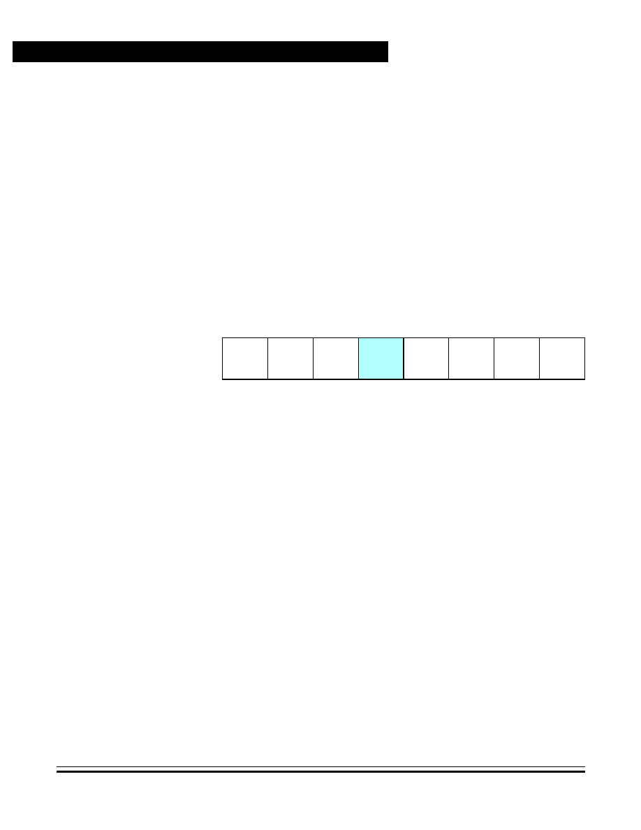
Technical Data
M68HC11K Family
96
Operating Modes and On-Chip Memory
MOTOROLA
Operating Modes and On-Chip Memory
4.8.1.2 Block Protect Register
This register prevents inadvertent writes to both the CONFIG register
and EEPROM. The active bits in this register are initialized to 1 out of
reset and can be cleared only during the first 64 E-clock cycles after
reset in the normal modes. When these bits are cleared, the associated
EEPROM section and the CONFIG register can be programmed or
erased. EEPROM is only visible if the EEON bit in the CONFIG register
is set. The bits in the BPROT register can be written to 1 at any time to
protect EEPROM and the CONFIG register. In test or bootstrap modes,
write protection is inhibited and BPROT can be written repeatedly.
BULKP -- Bulk Erase of EEPROM Protect Bit
0 = EEPROM can be bulk erased normally.
1 = EEPROM cannot be bulk or row erased.
LVPEN -- Low-Voltage Programming Protect Enable Bit
The functionality of LVPEN/LVPI was changed from earlier versions
of the M68HC11K Family. Setting this bit has no effect on the LVPI bit
in the PPROG register.
0 = Low-voltage programming inhibit (LVPI) for EEPROM disabled
1 = Low-voltage programming inhibit (LVPI) for EEPROM disabled
BPRT[4:0] -- Block Protect Bits for EEPROM Bits, see
Table 4-9
0 = Protection disabled for associated block
1 = Protection enabled for associated block
Address: $0035
Bit 7
6
5
4
3
2
1
Bit 0
Read:
BULKP
LVPEN
BPRT4
PTCON
BPRT3
BPRT2
BPRT1
BPRT0
Write:
Reset:
1
1
1
1
1
1
1
1
Figure 4-10. Block Protect Register (BPROT)
Operating Modes and On-Chip Memory
EEPROM and the CONFIG Register
M68HC11K Family
Technical Data
MOTOROLA
Operating Modes and On-Chip Memory
97
4.8.1.3 System Configuration Options Register
CSEL -- Clock Select Bit
Selects the built-in RC clock source for on-chip EEPROM and A/D
charge pumps. This clock should be used when the E clock falls
below 1 MHz.
0 = A/D and EEPROM use system E clock.
1 = A/D and EEPROM use internal RC clock.
4.8.2 EEPROM Programming
To write to any EEPROM byte, it must first be erased, for instance, all of
its bits must be set. A single byte, a row, or the entire EEPROM in a
single procedure can be erased by adjusting the BYTE and ROW bits in
PPROG. Once the targeted area has been erased, each byte can be
individually written.
Table 4-9. EEPROM Block Protect
Bit Name
Block Protected
Block Size
BPRT0
$xD80�$xD9F
32 bytes
BPRT1
$xDA0�$xDDF
64 bytes
BPRT2
$xDE0�$xE5F
128 bytes
BPRT3
$xE60�$xF7F
288 bytes
BPRT4
$xF80�$xFFF
128 bytes
Address: $0039
Bit 7
6
5
4
3
2
1
Bit 0
Read:
ADPU
CSEL
IRQE
DLY
(1)
CME
FCME
(1)
CR1
(1)
CR0
(1)
Write:
Reset:
0
0
0
1
0
0
0
0
1. Can be written only once in first 64 cycles out of reset in normal modes or at any time in
special modes.
Figure 4-11. System Configuration Options Register (OPTION)

Technical Data
M68HC11K Family
98
Operating Modes and On-Chip Memory
MOTOROLA
Operating Modes and On-Chip Memory
The procedures for both writing and erasing involve these five steps:
1. Set the EELAT bit in PPROG. If erasing, also set the ERASE bit
and the appropriate BYTE and ROW bits.
2. Write data to the appropriate EEPROM address. If erasing, any
data will work. To erase a row, write to any location in the row. To
erase the entire EEPROM, write to any location in the array. This
step is done before applying the programming voltage because
setting the EEPGM bit inhibits writes to EEPROM addresses.
3. Set the EEPGM bit in PPROG, keeping EELAT set. If erasing,
also set the ERASE bit and the appropriate BYTE and ROW bits.
4. Delay for 10 ms.
5. Clear the PPROG register to turn off the high voltage and
reconfigure the EEPROM address and data buses for normal
operation.
The following examples demonstrate programming a single EEPROM
byte, erasing the entire EEPROM, erasing a row (16 bytes), and erasing
a single byte.
4.8.2.1 EEPROM Programming
On entry, accumulator A contains the data to be written and X points to
the address to be programmed.
EEPROG
LDAB
#$02
STAB
$003B
Set EELAT bit to enable EEPROM
latches.
STAA
$0,X
Store data to EPROM address
LDAB
#$03
STAB
$002B
Set EPGM bit with ELAT=1
to enable EEPROM programming voltage
JSR
DLY10
Delay 10 ms
CLR
$003B
Turn off programming voltage and set
to READ mode

Operating Modes and On-Chip Memory
EEPROM and the CONFIG Register
M68HC11K Family
Technical Data
MOTOROLA
Operating Modes and On-Chip Memory
99
4.8.2.2 EEPROM Bulk Erase
BULKE
LDAB
#$06
STAB
$003B
Set EELAT and ERASE.
STAA
$0,X
Store any data to any EEPROM address
LDAB
#$07
STAB
$002B
Set EEPGM bit as well
to enable EEPROM programming voltage
JSR
DLY10
Delay 10 ms
CLR
$003B
Turn off programming voltage and set
to READ mode
4.8.2.3 EEPROM Row Erase
ROWE
LDAB
#$07
STAB
$003B
Set EELAT, ERASE and ROW.
STAA
$0,X
Store any data to any EEPROM address
in row
LDAB
#$07
STAB
$002B
Set EEPGM bit as well
to enable EEPROM programming voltage
JSR
DLY10
Delay 10 ms
CLR
$003B
Turn off programming voltage and set
to READ mode
4.8.2.4 EEPROM Byte Erase
BYTEE
LDAB
#$16
STAB
$003B
Set EELAT, ERASE and BYTE.
STAA
$0,X
Store any data to targeted EEPROM
address
LDAB
#$17
STAB
$002B
Set EEPGM bit as well
to enable EEPROM programming voltage
JSR
DLY10
Delay 10 ms
CLR
$003B
Turn off programming voltage and set
to READ mode
Technical Data
M68HC11K Family
100
Operating Modes and On-Chip Memory
MOTOROLA
Operating Modes and On-Chip Memory
4.8.3 CONFIG Register Programming
The CONFIG register is implemented with EEPROM cells, so EEPROM
procedures are required to change it. CONFIG can be programmed or
erased (including byte erase) while the MCU is operating in any mode,
provided that PTCON in BPROT is clear.
PTCON -- Protect for CONFIG Bit
0 = CONFIG register can be programmed or erased normally.
1 = CONFIG register cannot be programmed or erased.
To change the value in the CONFIG register, complete this procedure.
Do not initiate a reset until the procedure is complete.
�
Erase the CONFIG register.
�
Program the new value to the CONFIG address.
�
Initiate reset.
4.8.4 RAM and EEPROM Security
The NOSEC bit in the CONFIG register enables and disables an optional
security feature which protects the contents of EEPROM and RAM from
unauthorized access. This is done by restricting operation to single-chip
modes, preventing the memory locations from being monitored
externally. Single-chip modes do not allow visibility of the internal
address and data buses. Resident programs, however, have unlimited
access to the internal EEPROM and RAM and can read, write, or
transfer the contents of these memories.
Address: $0035
Bit 7
6
5
4
3
2
1
Bit 0
Read:
BULKP
LVPEN
BPRT4
PTCON
BPRT3
BPRT2
BPRT1
BPRT0
Write:
Reset:
1
1
1
1
1
1
1
1
Figure 4-12. Block Protect Register (BPROT)

Operating Modes and On-Chip Memory
EEPROM and the CONFIG Register
M68HC11K Family
Technical Data
MOTOROLA
Operating Modes and On-Chip Memory
101
NOTE:
CONFIG is writable once in normal modes and writable at any time in
special modes.
NOSEC -- RAM and EPROM Security Disabled Bit
0 = Enable security
1 = Disable security
M68HC11K Family devices are normally manufactured with NOSEC set
and the security option unavailable. However, on special request, a
mask option is selected during fabrication that enables the security
mode. The secure mode can be invoked on these parts by clearing
NOSEC. Contact a Motorola representative for information on the
availability of this feature.
The bootstrap program performs this sequence when the security
feature is present, enabled, and bootstrap mode is selected:
1. Output $FF, all 1s, on the SCI.
2. Clear the BPROT register by turning block protect off.
3. If the EEPROM is enabled, erase the EEPROM.
4. Verify that the EEPROM is erased. If EEPROM is not erased,
begin sequence again.
5. Write $FF, all 1s, to the entire block of RAM.
6. Erase the CONFIG register.
If all of the operations are successful, the bootload process continues as
if the device was never secured.
Address: $003F
Bit 7
6
5
4
3
2
1
Bit 0
Read:
ROMAD
1
CLKX
PAREN
NOSEC
NOCOP
ROMON
EEON
Write:
Reset:
--
1
--
--
1
--
--
--
Figure 4-13. System Configuration Register (CONFIG)
Technical Data
M68HC11K Family
102
Operating Modes and On-Chip Memory
MOTOROLA
Operating Modes and On-Chip Memory
4.9 XOUT Pin Control
The XOUT pin provides a buffered XTAL signal to synchronize external
devices with the MCU. It is enabled by the CLKX bit in the system
configuration (CONFIG) register. The frequency of XOUT can be divided
by one-of-four divisors selected by the XDV[1:0] bits in the system
configuration options 2 (OPT2) register. The XOUT pin is not configured
on all packages. Refer to the pin assignments in
Section 2. Pin
Description
.
4.9.1 System Configuration Register
Writable once in normal modes and writable at any time in special modes
CLKX -- XOUT Clock Enable Bit
The CLKX bit is a switch that enables a buffered clock running at the
same frequency as a referenced crystal. This buffered clock is
intended to synchronize external devices with the MCU.
0 = The XOUT pin is disabled.
1 = The X clock is driven out on the XOUT pin.
Address: $003F
Bit 7
6
5
4
3
2
1
Bit 0
Read:
ROMAD
1
CLKX
PAREN
NOSEC
NOCOP
ROMON
EEON
Write:
Reset:
--
1
--
--
1
--
--
--
Figure 4-14. System Configuration Register (CONFIG)
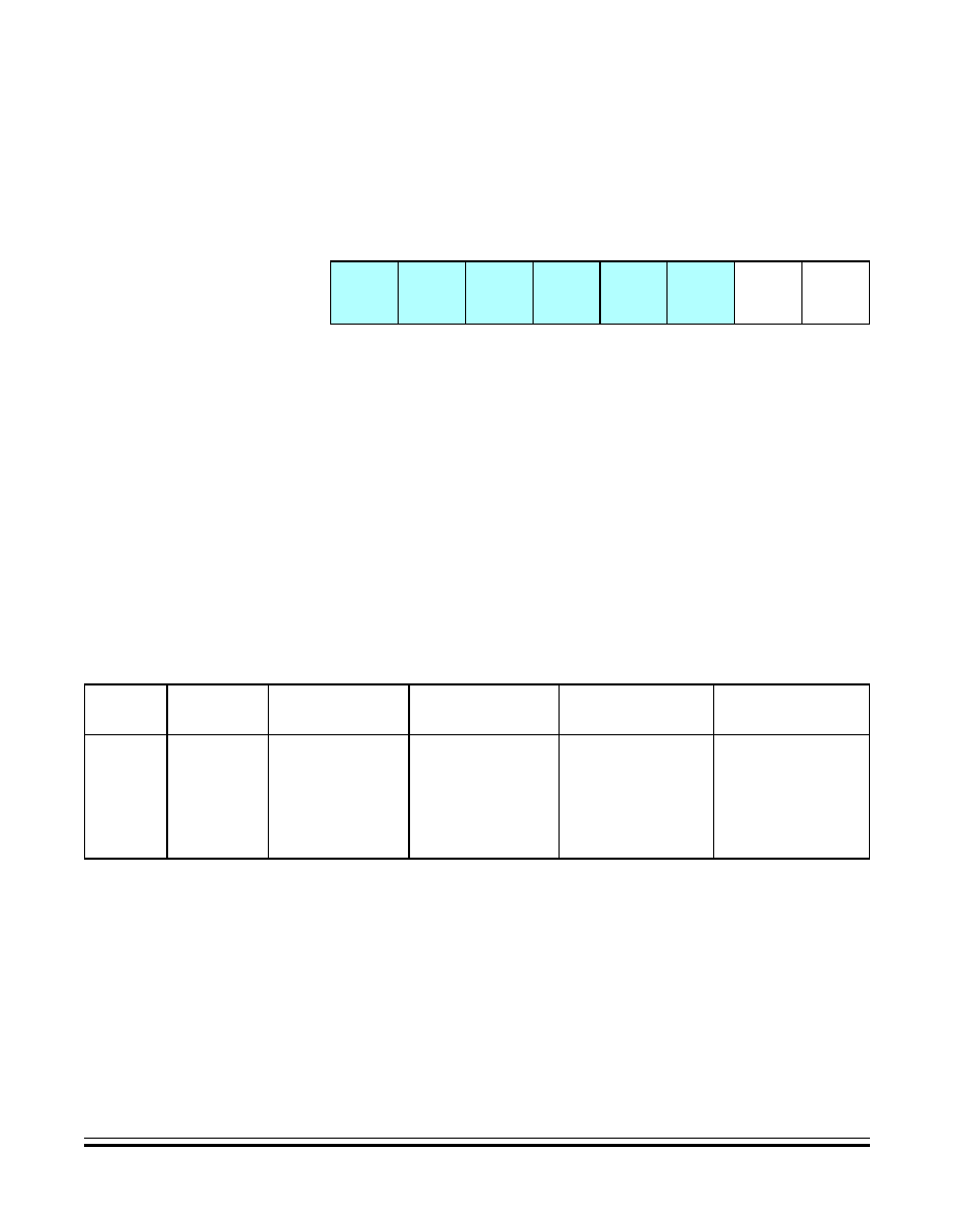
Operating Modes and On-Chip Memory
XOUT Pin Control
M68HC11K Family
Technical Data
MOTOROLA
Operating Modes and On-Chip Memory
103
4.9.2 System Configuration Options 2 Register
XDV[1:0] -- XOUT Clock Divide Select Bits
These two bits select the divisor for the XOUT clock frequency, as
shown in
Table 4-10
. The divisor is set to 1 out of reset
(XOUT = XTAL). It takes a maximum of 16 cycles after writing these
bits for XOUT to stabilize. The phase relationship between XOUT and
XTAL cannot be predicted.
Address: $0038
Bit 7
6
5
4
3
2
1
Bit 0
Read:
LIRDV
CWOM
STRCH
(1)
IRVNE
LSBF
SPR2
XDV1
XDV0
Write:
Reset:
0
0
0
--
0
0
0
0
1. Not available on M68HC11K devices
Figure 4-15. System Configuration Options 2 Register (OPT2)
Table 4-10. XOUT Frequencies
XDV[1:0]
EXTAL
Divided By
Frequency at
EXTAL = 8 MHz
Frequency at
EXTAL = 12 MHz
Frequency at
EXTAL = 16 MHz
Frequency at
EXTAL = 16 MHz
0
0
1
8 MHz
12 MHz
16 MHz
20 MHz
0
1
4
2 MHz
3 MHz
4 MHz
5 MHz
1
0
6
1.33 MHz
2 MHz
2.67 MHz
3.33 MHz
1
1
8
1 MHz
1.5 MHz
2 MHz
2.5 MHz

Technical Data
M68HC11K Family
104
Operating Modes and On-Chip Memory
MOTOROLA
Operating Modes and On-Chip Memory

M68HC11K Family
Technical Data
MOTOROLA
Resets and Interrupts
105
Technical Data -- M68HC11K Family
Section 5. Resets and Interrupts
5.1 Contents
5.2
Introduction . . . . . . . . . . . . . . . . . . . . . . . . . . . . . . . . . . . . . . . 106
5.3
Sources of Resets . . . . . . . . . . . . . . . . . . . . . . . . . . . . . . . . . 106
5.3.1
Power-On Reset (POR) . . . . . . . . . . . . . . . . . . . . . . . . . . . 107
5.3.2
External Reset (RESET) . . . . . . . . . . . . . . . . . . . . . . . . . . 107
5.3.3
Computer Operating Properly (COP) System . . . . . . . . . . 107
5.3.3.1
System Configuration Register . . . . . . . . . . . . . . . . . . . 108
5.3.3.2
System Configuration Options Register . . . . . . . . . . . . . 109
5.3.3.3
Arm/Reset COP Timer Circuitry Register. . . . . . . . . . . . 110
5.3.4
Clock Monitor Reset . . . . . . . . . . . . . . . . . . . . . . . . . . . . . . 110
5.3.4.1
System Configuration Options Register . . . . . . . . . . . . . 111
5.3.4.2
System Configuration Options Register 2 . . . . . . . . . . . 112
5.4
Effects of Reset . . . . . . . . . . . . . . . . . . . . . . . . . . . . . . . . . . . 115
5.5
Interrupts. . . . . . . . . . . . . . . . . . . . . . . . . . . . . . . . . . . . . . . . . 117
5.5.1
Non-Maskable Interrupts . . . . . . . . . . . . . . . . . . . . . . . . . . 120
5.5.1.1
Non-Maskable Interrupt Request (XIRQ) . . . . . . . . . . . . 120
5.5.1.2
Illegal Opcode Trap . . . . . . . . . . . . . . . . . . . . . . . . . . . . 120
5.5.1.3
Software Interrupt (SWI) . . . . . . . . . . . . . . . . . . . . . . . . 121
5.5.2
Maskable Interrupts . . . . . . . . . . . . . . . . . . . . . . . . . . . . . . 121
5.6
Reset and Interrupt Priority. . . . . . . . . . . . . . . . . . . . . . . . . . . 122
5.7
Reset and Interrupt Processing . . . . . . . . . . . . . . . . . . . . . . .123
5.8
Low-Power Operation . . . . . . . . . . . . . . . . . . . . . . . . . . . . . . . 129
5.8.1
Wait Mode . . . . . . . . . . . . . . . . . . . . . . . . . . . . . . . . . . . . .130
5.8.2
Stop Mode . . . . . . . . . . . . . . . . . . . . . . . . . . . . . . . . . . . . .130
5.8.3
Slow Mode . . . . . . . . . . . . . . . . . . . . . . . . . . . . . . . . . . . . .132
Technical Data
M68HC11K Family
106
Resets and Interrupts
MOTOROLA
Resets and Interrupts
5.2 Introduction
When a reset or interrupt occurs, the microcontroller (MCU) retrieves the
starting address of a program or interrupt routine from a vector table in
memory and loads it in the program counter. A reset immediately stops
execution of the current instruction and reinitializes the control registers.
An interrupt preserves the current program status, performs an interrupt
service routine, and resumes operation as if there had been no
interruption.
5.3 Sources of Resets
The four sources of reset are:
�
Power-on reset (POR)
�
External reset (RESET)
�
Computer operating properly (COP) system
�
Clock monitor
NOTE:
Power-on reset and external reset share the same interrupt vectors.
The CPU fetches a restart vector during the first three clock cycles after
reset and begins executing instructions. Vector selection is based on the
type of reset and operating mode, as shown in
Table 5-1
.
Table 5-1. Reset Vectors
Operating
Mode
POR or RESET
Clock Monitor
COP Watchdog
Normal
$FFFE and $FFFF
$FFFC and $FFFD
$FFFA and $FFFB
Test or bootstrap
$BFFE and $BFFF
$BFFC and $BFFD
$BFFA and $BFFB

Resets and Interrupts
Sources of Resets
M68HC11K Family
Technical Data
MOTOROLA
Resets and Interrupts
107
5.3.1 Power-On Reset (POR)
A positive transition on V
DD
generates a POR, which is used only for
power-up conditions. POR cannot be used to detect drops in power
supply voltages. The CPU delays 4064 internal clock cycles after the
oscillator becomes active to allow the clock generator to stabilize, then
checks the RESET pin. If RESET is at logical 0, the CPU remains in the
reset condition until the RESET pin goes to logical 1.
5.3.2 External Reset (RESET)
The CPU distinguishes between internal and external reset conditions
by sensing whether the reset pin rises to a logic 1 in less than two
E-clock cycles after an internal device releases reset. When a reset
condition is sensed, the RESET pin is driven low by an internal device
for four E-clock cycles, then released. Two E-clock cycles later, it is
sampled. If the pin is still held low, the CPU assumes that an external
reset has occurred. If the pin is high, it indicates that the reset was
initiated internally by either the COP system or the clock monitor.
NOTE:
It is not advisable to connect an external resistor capacitor (RC)
power-up delay circuit to the reset pin of M68HC11 devices because the
circuit charge time constant can cause the device to misinterpret the
type of reset that occurred.
5.3.3 Computer Operating Properly (COP) System
The MCU includes a COP system to help protect against software
failures. When the COP is enabled, software periodically reinitializes a
free-running watchdog timer before it times out and resets the system.
Such a system reset indicates that a software error has occurred.
Technical Data
M68HC11K Family
108
Resets and Interrupts
MOTOROLA
Resets and Interrupts
Three registers are involved in COP operation:
�
The CONFIG register contains a bit which determines whether the
COP system is enabled or disabled.
�
The OPTION register contains two bits which determine the COP
timeout period.
�
The COPRST register must be written by software to reset the
watchdog timer.
NOTE:
Throughout this manual, the registers are discussed by function. In the
event that not all bits in a register are referenced, the bits that are not
discussed are shaded.
5.3.3.1 System Configuration Register
In normal modes, COP is enabled out of reset and does not depend on
software action. To disable the COP system, set the NOCOP bit in the
CONFIG register (see
Figure 5-1
). In special test and bootstrap
operating modes, the COP system is initially inhibited by the disable
resets (DISR) control bit in the TEST1 register. The DISR bit can
subsequently be written to 0 to enable COP resets.
NOTE:
CONFIG is writable once in normal modes and writable at any time in
special modes.
NOCOP -- COP System Disable Bit
0 = COP enabled
1 = COP disabled
Address: $003F
Bit 7
6
5
4
3
2
1
Bit 0
Read:
ROMAD
1
CLKX
PAREN
NOSEC
NOCOP
ROMON
EEON
Write:
Reset:
--
1
--
--
1
--
--
--
Figure 5-1. System Configuration Register (CONFIG)
Resets and Interrupts
Sources of Resets
M68HC11K Family
Technical Data
MOTOROLA
Resets and Interrupts
109
5.3.3.2 System Configuration Options Register
Two bits in the OPTION register select one of four values for the COP
timer.
CR[1:0] -- COP Timer Rate Select Bits
The MCU derives the counter for the COP timer by dividing the
system E clock by 2
15
and applying a further scaling factor selected
by CR[1:0] as shown in
Table 5-2
. After reset, these bits are 0, and
that condition selects the fastest timeout period.
NOTE:
In normal operating modes, these bits can be written only once within 64
bus cycles after reset.
Address: $0039
Bit 7
6
5
4
3
2
1
Bit 0
Read:
ADPU
CSEL
IRQE
DLY
CME
FCME
CR1
CR0
Write:
Reset:
0
0
0
1
0
0
0
0
Figure 5-2. System Configuration Options Register (OPTION)
Table 5-2. COP Timeout
EXTAL Frequencies
EXTAL Freq.
8.0 MHz
12.0 MHz
16.0 MHz
20.0 MHz
24.0 MHz
Other EXTAL
E Clock Freq.
2.0 MHz
3.0 MHz
4.0 MHz
5.0 MHz
6.0 MHz
EXTAL
�
4
Control Bits
SPR[2:0]
COP Timeout
Timeout
0/+16.384 ms
0/+10.923 ms
0/+8.192 ms
0/+6.544 ms
0/+5.461 ms
0/+2
15
�
E
0 0
16.384 ms
10.923 ms
8.192 ms
6.554 ms
5.461 ms
2
15
�
E
0 1
65.536 ms
43.691 ms
32.768 ms
26.214 ms
21.845 ms
2
17
�
E
1 0
262.144 ms
174.763 ms
131.072 ms
104.858 ms
87.381 ms
2
19
�
E
1 1
1.049 sec
699.051 ms
524.288 ms
419.430 ms
349.525 ms
2
21
�
E

Technical Data
M68HC11K Family
110
Resets and Interrupts
MOTOROLA
Resets and Interrupts
5.3.3.3 Arm/Reset COP Timer Circuitry Register
To prevent a COP reset, this sequence must be completed:
1. Write $55 to COPRST to arm the COP timer clearing mechanism.
2. Write $AA to COPRST to clear the COP timer.
NOTE:
Performing instructions between these two steps is possible as long as
both steps are completed in the correct sequence before the timer times
out.
5.3.4 Clock Monitor Reset
The clock monitor can serve as a backup for the COP system. Its circuit
is based on an internal RC time delay. If no MCU clock edges are
detected within this RC time delay, the clock monitor generates a system
reset. Because the COP needs a clock to function, it is disabled when
the clocks stop. Thus, the clock monitor system can detect clock failures
not detected by the COP system.
Address: $003A
Bit 7
6
5
4
3
2
1
Bit 0
Read:
Bit 7
Bit 6
Bit 5
Bit 4
Bit 3
Bit 2
Bit 1
Bit 0
Write:
Reset:
0
0
0
0
0
0
0
0
Figure 5-3. Arm/Reset COP Timer Circuitry Register (COPRST)
Resets and Interrupts
Sources of Resets
M68HC11K Family
Technical Data
MOTOROLA
Resets and Interrupts
111
5.3.4.1 System Configuration Options Register
The clock monitor function is enabled or disabled by the CME control bit
in the OPTION register (see
Figure 5-4
). The FCME bit in OPTION
overrides CME and enables the clock monitor until the next reset.
NOTE:
In normal operating modes, these bits can be written only once within 64
bus cycles after reset.
CME -- Clock Monitor Enable Bit
This control bit can be read or written at any time and controls whether
or not the internal clock monitor circuit triggers a reset sequence when
the system clock is slow or absent. When it is clear, the clock monitor
circuit is disabled. When it is set, the clock monitor circuit is enabled.
Reset clears the CME bit.
0 = Clock monitor disabled
1 = Clock monitor enabled
FCME -- Force Clock Monitor Enable Bit
0 = Clock monitor follows the state of the CME bit.
1 = Clock monitor is enabled until the next reset.
Semiconductor wafer processing causes variations of the RC timeout
values between individual devices. An E-clock frequency below 10 kHz
generates a clock monitor error. An E-clock frequency of 200 kHz or
more prevents clock monitor errors. Using the clock monitor function
when the E clock is below 200 kHz is not recommended.
Address: $0030
Bit 7
6
5
4
3
2
1
Bit 0
Read:
ADPU
CSEL
IRQE
DLY
CME
FCME
CR1
CR0
Write:
Reset:
0
0
0
1
0
0
0
0
Figure 5-4. System Configuration Options Register (OPTION)

Technical Data
M68HC11K Family
112
Resets and Interrupts
MOTOROLA
Resets and Interrupts
5.3.4.2 System Configuration Options Register 2
LIRDV -- LIR Driven Bit
This bit allows power savings in expanded modes by turning off the
LIR output (it has no meaning in single-chip or bootstrap modes). The
LIR pin is driven low to indicate that execution of an instruction has
begun. To detect consecutive instructions in a high-speed application,
this signal drives high for a quarter of a cycle to prevent false
triggering. An external pullup is required in expanded modes, while a
hardwired V
SS
connection is possible in single-chip modes. LIRDV is
reset to 0 in single-chip modes and to 1 in expanded modes.
1 = Enable LIR push-pull drive
0 = LIR not driven high on MODA/LIR pin
CWOM -- Port C Wired-OR Mode Bit
For detailed information, refer to
Section 6. Parallel Input/Output
.
1 = Port C outputs are open drain.
0 = Port C operates normally.
STRCH -- Stretch External Accesses Bit
When this bit is set, off-chip accesses of selected addresses are
extended by one E-clock cycle to allow access to slow peripherals.
The E clock stretches externally, but the internal clocks are not
affected, so that timers and serial systems are not corrupted. The
state of the ROMAD bit in the CONFIG register determines which
address range is affected.
1 = Off-chip accesses are selectively extended by one E-clock
cycle.
0 = Normal operation
Address: $0038
Bit 7
6
5
4
3
2
1
Bit 0
Read:
LIRDV
CWOM
STRCH
(1)
IRVNE
LSBF
SPR2
XDV1
XDV0
Write:
Reset:
0
0
0
--
0
0
0
0
1. Not available on M68HC11K devices
Figure 5-5. System Configuration Options Register 2 (OPT2)
Resets and Interrupts
Sources of Resets
M68HC11K Family
Technical Data
MOTOROLA
Resets and Interrupts
113
NOTE:
STRCH is cleared on reset; therefore, a program cannot execute out of
reset in a slow external ROM.
To use the STRCH feature, ROMON must be set on reset so that the
device starts with internal ROM included in the memory map. STRCH
should then be set.
STRCH has no effect in single-chip and bootstrap modes.
NOTE:
STRCH is not available on M68HC11K devices.
IRVNE -- Internal Read Visibility/Not E Bit
IRVNE can be written once in any user mode. In expanded modes,
IRVNE determines whether IRV is on or off (but has no meaning in
user expanded secure mode, as IRV must be disabled). In special test
mode, IRVNE is reset to 1. In normal modes, IRVNE is reset to 0.
1 = Data from internal reads is driven out of the external data bus.
0 = No visibility of internal reads on external bus
In single-chip modes, this bit determines whether the E clock drives
out from the chip.
1 = E pin is driven low.
0 = E clock is driven out from the chip.
Refer to
Table 5-3
for a summary of the operation immediately
following reset.
Table 5-3. IRVNE Operation After Reset
Mode
IRVNE
after
Reset
E Clock
after
Reset
IRV
after
Reset
IRVNE
Affects
Only
IRVNE
Can Be
Written
Single-chip
0
On
Off
E
Once
Expanded
0
On
Off
IRV
Once
Bootstrap
0
On
Off
E
Unlimited
Special test
1
On
On
IRV
Unlimited
Technical Data
M68HC11K Family
114
Resets and Interrupts
MOTOROLA
Resets and Interrupts
LSBF -- Least Significant Bit (LSB) First Enable Bit
For detailed information, refer to
Section 8. Serial Peripheral
Interface (SPI)
.
1 = Data is transferred LSB first.
0 = Data is transferred MSB (most significant bit) first.
SPR2 -- SPI Clock Rate Selected Bit
This bit adds a divide-by-four to the SPI clock chain. For detailed
information, refer to
Section 8. Serial Peripheral Interface (SPI)
.
XDV[1:0] -- XOUT Clock Divide Select Bits
These bits control the frequency of the clock driven out of the
XOUT pin, if enabled by the CLKX bit on the CONFIG register. See
Table 5-4
Table 5-4. XOUT Clock Divide Select
XDV
[1:0]
XOUT = EXTAL
Divided By
Frequency at
EXTAL =
8 MHz
Frequency at
EXTAL =
12 MHz
Frequency at
EXTAL =
16 MHz
0 0
1
8 MHz
12 MHz
16 MHz
0 1
4
2 MHz
3 MHz
4 MHz
1 0
6
1.3 MHz
2 MHz
2.7 MHz
1 1
8
1 MHz
1.5 MHz
2 MHz

Resets and Interrupts
Effects of Reset
M68HC11K Family
Technical Data
MOTOROLA
Resets and Interrupts
115
5.4 Effects of Reset
When the MCU recognizes a reset condition, it forces the CPU registers
and control bits to established initial states. These in turn force the
on-chip peripheral systems to known startup states, as described here.
�
Central processor unit (CPU)
�
The stack pointer and other CPU registers are indeterminate
immediately after reset, except for three bits in the condition
code register (CCR).
�
The X and I interrupt mask bits are set to mask any interrupt
requests, and the S bit in the CCR is set to inhibit the stop
mode.
�
Memory map
�
The INIT register is initialized to $00, putting the control
registers at locations $0000�$007F.
�
The 1.5 Kbytes of RAM are at locations $0080�$067F except
for the M68HC11KS Family, which has 1 Kbytes of RAM at
locations $0080�$047F.
�
The INIT2 register is $00, locating the EEPROM at
$0D80�$0FFF.
�
Timer
�
The timing system is initialized to a count of $0000.
�
The prescaler bits are cleared, and all output compare
registers are initialized to $FFFF.
�
All input capture registers are indeterminate after reset.
�
The output compare 1 mask (OC1M) register is cleared so that
successful OC1 compares do not affect any input/output (I/O)
pins. The other four output compares are configured so that
they do not affect any I/O pins on successful compares.
�
All input capture edge-detector circuits are configured for
capture disabled operation.
�
The timer overflow interrupt flag and all eight timer function
interrupt flags are cleared.

Technical Data
M68HC11K Family
116
Resets and Interrupts
MOTOROLA
Resets and Interrupts
�
All nine timer interrupts are disabled because their mask bits
have been cleared.
�
The I4/O5 bit in the PACTL register is cleared to configure the
I4/O5 function as OC5; however, the OM5:OL5 control bits in
the TCTL1 register are clear so OC5 does not control the PA3
pin.
�
Real-time interrupt (RTI)
�
The RTI enable bit in TMSK2 is cleared, masking automatic
hardware interrupts.
�
The rate control bits are cleared after reset and can be
initialized by software before the RTI system is enabled.
�
Pulse accumulator
�
The pulse accumulator system is disabled at reset.
�
The PAI input pin defaults to a general-purpose input pin
(PA7).
�
Computer operating properly (COP) watchdog system
�
The COP watchdog system is enabled if the NOCOP control
bit in the CONFIG register is clear and disabled if NOCOP is
set.
�
The OPTION register's CR[1:0] bits are cleared, setting the
COP rate for the shortest duration timeout.
�
Serial communications interface (SCI)
�
At reset, the SCI baud rate control register (
7.9.1 SCI Baud
Rate Control Register
) is initialized to $0004.
�
All transmit and receive interrupts are masked and both the
transmitter and receiver are disabled so the port pins default to
being general-purpose I/O lines.
�
The SCI frame format is initialized to an 8-bit character size.
�
The send break and receiver wake-up functions are disabled.
�
The TDRE and TC status bits in the SCI status register are
both set, indicating that there is no transmit data in either the
transmit data register or the transmit serial shift register.

Resets and Interrupts
Interrupts
M68HC11K Family
Technical Data
MOTOROLA
Resets and Interrupts
117
�
The RDRF, IDLE, OR, NF, FE, PF, and RAF receive-related
status bits are cleared.
�
Serial peripheral interface (SPI)
�
The SPI system is disabled by reset.
�
The port pins associated with this function default to being
general-purpose I/O lines.
�
Analog-to-digital (A/D) converter
�
The ADPU bit in the OPTION register is cleared, disabling the
A/D system.
�
The conversion complete flag in the ADCTL register is also
cleared.
�
System
�
The external IRQ pin has the highest I-bit interrupt priority
because PSEL[4:0] in the HPRIO register are initialized with
the value %00110 (where % indicates a binary value).
�
The RBOOT, SMOD, and MDA bits in the HPRIO register
reflect the status of the MODB and MODA inputs at the rising
edge of reset.
�
The IRQ pin is configured for level-sensitive operation for
wired-OR systems.
�
The DLY control bit in the OPTION register is set, enabling
oscillator startup delay after recovery from stop mode.
�
The clock monitor system is disabled because the CME and
FCME bits in the OPTION register are cleared.
5.5 Interrupts
The MCU has 18 interrupt vectors that support 22 interrupt sources. The
19 maskable interrupts are generated by on-chip peripheral systems.
They are recognized when the I bit in the CCR is clear. The three
non-maskable interrupt sources are illegal opcode trap, software
interrupt, and XIRQ pin.
Table 5-5
lists the interrupt sources and vector
assignments for each source.
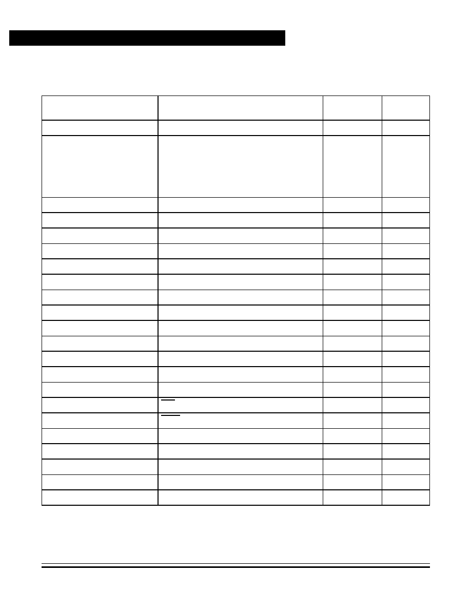
Technical Data
M68HC11K Family
118
Resets and Interrupts
MOTOROLA
Resets and Interrupts
Table 5-5. Interrupt and Reset Vector Assignments
Vector Address
Interrupt Source
CC Register
Mask
Local
Mask
FFC0, C1 -- FFD4, D5
Reserved
--
--
FFD6, D7
SCI serial system:
�
SCI transmit complete
�
SCI transmit data register empty
�
SCI idle line detect
�
SCI receiver overrun
�
SCI receive data register full
I bit
TCIE
TIE
ILIE
RIE
RIE
FFD8, D9
SPI serial transfer complete
I bit
SPIE
FFDA, DB
Pulse accumulator input edge
I bit
PAII
FFDC, DD
Pulse accumulator overflow
I bit
PAOVI
FFDE, DF
Timer overflow
I bit
TOI
FFE0, E1
Timer input capture 4/output compare 5
I bit
I4/O5I
FFE2, E3
Timer output compare 4
I bit
OC4I
FFE4, E5
Timer output compare 3
I bit
OC3I
FFE6, E7
Timer output compare 2
I bit
OC2I
FFE8, E9
Timer output compare 1
I bit
OC1I
FFEA, EB
Timer input capture 3
I bit
IC3I
FFEC, ED
Timer input capture 2
I bit
IC2I
FFEE, EF
Timer input capture 1
I bit
IC1I
FFF0, F1
Real-time interrupt
I bit
RTII
FFF2, F3
IRQ (external pin)
I bit
None
FFF4, F5
XIRQ pin
X bit
None
FFF6, F7
Software interrupt
None
None
FFF8, F9
Illegal opcode trap
None
None
FFFA, FB
COP failure
None
NOCOP
FFFC, FD
Clock monitor fail
None
CME
FFFE, FF
RESET
None
None
Resets and Interrupts
Interrupts
M68HC11K Family
Technical Data
MOTOROLA
Resets and Interrupts
119
Many interrupt sources set associated flag bits when interrupts occur.
These flags are usually cleared during the course of normal interrupt
service. For example, the normal response to an RDRF interrupt request
in the SCI is to read the SCI status register to check for receive errors,
then read the received data from the SCI data register. It is precisely
these two steps which clear RDRF, so no extra steps are required.
An interrupt can be recognized at any time after it is enabled by its local
mask, if any, and by the global mask bit in the CCR. The CPU responds
to an interrupt at the completion of the instruction being executed. Since
the number of clock cycles in the instruction varies, so does interrupt
latency. The CPU pushes the contents of its registers onto the stack in
the order shown in
Table 5-6
. After the CCR value is stacked, the I bit is
set (and the X bit as well if XIRQ is pending) to inhibit further interrupts.
The CPU fetches the interrupt vector for the highest priority pending
source, and execution continues at the address specified by the vector.
The interrupt service routine ends with the return-from-interrupt (RTI)
instruction, which tells the CPU to pull the saved registers from the stack
in reverse order so that normal program execution can resume.
Table 5-6. Stacking Order on Entry to Interrupts
Memory Location
CPU Registers
SP
PCL
SP � 1
PCH
SP �2
IYL
SP � 3
IYH
SP � 4
IXL
SP � 5
IXH
SP � 6
ACCA
SP � 7
ACCB
SP � 8
CCR

Technical Data
M68HC11K Family
120
Resets and Interrupts
MOTOROLA
Resets and Interrupts
5.5.1 Non-Maskable Interrupts
Non-maskable interrupts can interrupt CPU operations at any time. The
most common use for such an interrupt is for serious system problems,
such as program runaway or power failure. The three sources of
non-maskable interrupt are:
�
XIRQ pin
�
Illegal opcode trap
�
Software interrupt instruction (SWI)
5.5.1.1 Non-Maskable Interrupt Request (XIRQ)
The XIRQ input is an updated version of the non-maskable NMI input of
earlier MCUs. Upon reset, both the X bit and I bit of the CCR are set to
inhibit all maskable interrupts and XIRQ. After minimum system
initialization, software can clear the X bit by a transfer from accumulator
A to condition code register (TAP) instruction, enabling XIRQ interrupts.
Thereafter, software cannot set the X bit and the XIRQ interrupt
becomes non-maskable.
I bit-related interrupts do not affect the X bit, which has a higher priority
than they do in the interrupt priority logic. When an I bit-related interrupt
occurs, the CPU sets the I bit after stacking the CCR byte, but the X bit
remains unaffected. When an X bit-related interrupt occurs, the CPU
sets both the X and I bits after stacking the CCR. The RTI instruction
restores the X and I bits to their pre-interrupt request state when it pulls
the CCR from the stack.
5.5.1.2 Illegal Opcode Trap
The MCU includes an illegal opcode detection circuit to avoid attempting
to process undefined opcodes or opcode sequences. This mechanism
works for all unimplemented opcodes on all four opcode map pages.
When the circuit detects an illegal opcode, it generates an interrupt. The
CPU responds by pushing the current value of the program counter,
which is actually the address of the first byte of the illegal opcode, on the
stack. The illegal opcode service routine can use this stacked address
as a pointer to the illegal opcode to correct it. To avoid repeated

Resets and Interrupts
Interrupts
M68HC11K Family
Technical Data
MOTOROLA
Resets and Interrupts
121
execution of the illegal opcode, which can lead to stack overflow, the
service routine should reinitialize the stack pointer.
5.5.1.3 Software Interrupt (SWI)
SWI cannot be masked by virtue of the fact that it is a software
instruction. It is not inhibited by the global mask bits in the CCR.
Execution of SWI sets the I mask bit, so other interrupts are inhibited
until user software clears the I bit or SWI terminates with an RTI
instruction.
5.5.2 Maskable Interrupts
All maskable interrupts are generated by on-chip peripherals, with the
exception of the IRQ pin. This input can be connected through a
wired-OR network to external devices. When one of these devices pulls
IRQ low, a software accessible interrupt flag is set. When enabled, this
flag causes a constant request for interrupt service. After the flag is
cleared, the service request is released. IRQ is low-level sensitive by
default, but can be set for falling-edge sensitivity by the IRQE bit in the
OPTION register (see
Figure 5-6
).
IRQE -- Configure IRQ for Edge-Sensitive Operation Bit
This bit can be written only once during the first 64 E-clock cycles after
reset in normal modes.
0 = Low-level recognition
1 = Falling-edge recognition
Address: $0039
Bit 7
6
5
4
3
2
1
Bit 0
Read:
ADPU
CSEL
IRQE
(1)
DLY
(1)
CME
FCME
(1)
CR1
(1)
CR0
(1)
Write:
Reset:
0
0
0
1
0
0
0
0
1. Can be written only once in first 64 cycles out of reset in normal modes or at any time in
special modes
Figure 5-6. System Configuration Options Register (OPTION)

Technical Data
M68HC11K Family
122
Resets and Interrupts
MOTOROLA
Resets and Interrupts
5.6 Reset and Interrupt Priority
A hardware priority scheme determines which reset or interrupt is
serviced first when simultaneous requests occur.
The six highest-priority interrupt sources are not maskable. The priority
arrangement for these sources is:
1. POR or RESET pin
2. Clock monitor reset
3. COP watchdog reset
4. XIRQ interrupt
5. Illegal opcode interrupt
6. Software interrupt (SWI)
The maskable interrupt sources have this priority arrangement:
1. IRQ
2. Real-time interrupt
3. Timer input capture 1
4. Timer input capture 2
5. Timer input capture 3
6. Timer output compare 1
7. Timer output compare 2
8. Timer output compare 3
9. Timer output compare 4
10. Timer input capture 4/output compare 5
11. Timer overflow
12. Pulse accumulator overflow
13. Pulse accumulator input edge
14. SPI transfer complete
15. SCI system

Resets and Interrupts
Reset and Interrupt Processing
M68HC11K Family
Technical Data
MOTOROLA
Resets and Interrupts
123
Any single maskable interrupt can be given priority over other maskable
interrupts by writing the appropriate value to the PSEL bits in the HPRIO
register (see
Figure 5-7
). An interrupt that is assigned highest priority is
still subject to global masking by the I bit in the CCR or by any associated
local bits. Interrupt vectors are not affected by priority assignment.
NOTE:
To avoid race conditions, HPRIO is designed so that bits PSEL[4:0] can
be written only while the I-bit is set (interrupts are inhibited).
PSEL[4:0] -- Priority Select Bits
These bits select one interrupt source to have the highest priority, as
explained in
Table 5-7
.
5.7 Reset and Interrupt Processing
This section presents flow diagrams of the reset and interrupt processes.
Figure 5-8
illustrates how the CPU begins from a reset and how interrupt
detection relates to normal opcode fetches.
Figure 5-9
is an expansion
of a block in
Figure 5-8
and illustrates interrupt priorities.
Figure 5-10
shows the resolution of interrupt sources within the SCI subsystem.
Address: $003C
Bit 7
6
5
4
3
2
1
Bit 0
Read:
RBOOT
SMOD
MDA
PSEL4
PSEL3
PSEL2
PSEL1
PSEL0
Write:
Reset:
0
0
0
0
0
1
1
0
Figure 5-7. Highest Priority I-Bit Interrupt
and Miscellaneous Register (HPRIO)
Technical Data
M68HC11K Family
124
Resets and Interrupts
MOTOROLA
Resets and Interrupts
Table 5-7. Highest Priority Interrupt Selection
PSELx
Interrupt Source Promoted
4
3
2
1
0
0
0
0
X
X
Reserved (default to IRQ)
0
0
1
0
0
Reserved (default to IRQ)
0
0
1
0
1
Reserved (default to IRQ)
0
0
1
1
0
IRQ
0
0
1
1
1
Real-time interrupt
0
1
0
0
0
Timer input capture 1
0
1
0
0
1
Timer input capture 2
0
1
0
1
0
Timer input capture 3
0
1
0
1
1
Timer output compare 1
0
1
1
0
0
Timer output compare 2
0
1
1
0
1
Timer output compare 3
0
1
1
1
0
Timer output compare 4
0
1
1
1
1
Timer output compare 5/input capture 4
1
0
0
0
0
Timer overflow
1
0
0
0
1
Pulse accumulator overflow
1
0
0
1
0
Pulse accumulator input edge
1
0
0
1
1
SPI serial transfer complete
1
0
1
0
0
SCI serial system
1
0
1
0
1
Reserved (default to IRQ)
1
0
1
1
0
Reserved (default to IRQ)
1
0
1
1
1
Reserved (default to IRQ)
1
1
X
X
X
Reserved (default to IRQ)
Resets and Interrupts
Reset and Interrupt Processing
M68HC11K Family
Technical Data
MOTOROLA
Resets and Interrupts
125
Figure 5-8. Processing Flow Out of Reset (Sheet 1 of 2)
2A
BIT X IN
Y
N
XIRQ
Y
N
PIN LOW?
CCR = 1?
BEGIN INSTRUCTION
SEQUENCE
1A
STACK CPU
REGISTERS
SET BITS I AND X
FETCH VECTOR
$FFF4, $FFF5
SET BITS S, I, AND X
RESET MCU
HARDWARE
POWER-ON RESET
(POR)
EXTERNAL RESET
CLOCK MONITOR FAIL
(WITH CME = 1)
COP WATCHDOG
TIMEOUT
(WITH NOCOP = 0)
DELAY 4064 E CYCLES
LOAD PROGRAM COUNTER
WITH CONTENTS OF
$FFFE, $FFFF
(VECTOR FETCH)
LOAD PROGRAM COUNTER
WITH CONTENTS OF
$FFFC, $FFFD
(VECTOR FETCH)
LOAD PROGRAM COUNTER
WITH CONTENTS OF
$FFFA, $FFFB
(VECTOR FETCH)
HIGHEST
PRIORITY
LOWEST
PRIORITY
Technical Data
M68HC11K Family
126
Resets and Interrupts
MOTOROLA
Resets and Interrupts
Figure 5-8. Processing Flow Out of Reset (Sheet 2 of 2)
BIT I IN
CCR = 1?
2A
Y
N
ANY I-BIT
INTERRUPT
Y
N
PENDING?
FETCH OPCODE
ILLEGAL
OPCODE?
Y
N
WAI
Y
N
INSTRUCTION?
SWI
INSTRUCTION?
Y
N
RTI
INSTRUCTION?
Y
N
EXECUTE THIS
INSTRUCTION
STACK CPU
REGISTERS
ANY
N
Y
INTERRUPT
PENDING?
SET BIT I IN CCR
RESOLVE INTERRUPT
PRIORITY AND FETCH
VECTOR FOR HIGHEST
PENDING SOURCE
STACK CPU
REGISTERS
SET BIT I IN CCR
FETCH VECTOR
$FFF8, $FFF9
STACK CPU
REGISTERS
SET BIT I IN CCR
FETCH VECTOR
$FFF6, $FFF7
RESTORE CPU
REGISTERS
FROM STACK
1A
STACK CPU
REGISTERS
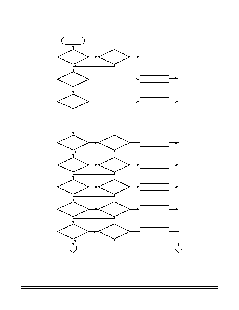
Resets and Interrupts
Reset and Interrupt Processing
M68HC11K Family
Technical Data
MOTOROLA
Resets and Interrupts
127
Figure 5-9. Interrupt Priority Resolution (Sheet 1 of 2)
2A
BEGIN
SET X BIT IN CCR
FETCH VECTOR
$FFF4, FFF5
X BIT
IN CCR
SET ?
YES
NO
XIRQ PIN
LOW ?
YES
NO
HIGHEST
PRIORITY
INTERRUPT
?
YES
NO
IRQ ?
YES
NO
FETCH VECTOR
$FFF2, FFF3
FETCH VECTOR
$FFF0, FFF1
RTII = 1 ?
YES
NO
REAL-TIME
INTERRUPT
?
YES
NO
FETCH VECTOR
$FFEE, FFEF
IC1I = 1 ?
YES
NO
TIMER
IC1F ?
YES
NO
FETCH VECTOR
$FFEC, FFED
IC2I = 1 ?
YES
NO
TIMER
IC2F ?
YES
NO
FETCH VECTOR
$FFEA, FFEB
IC3I = 1 ?
YES
NO
TIMER
IC3F ?
YES
NO
FETCH VECTOR
$FFE8, FFE9
OC1I = 1 ?
YES
NO
TIMER
OC1F ?
YES
NO
2B
FETCH VECTOR
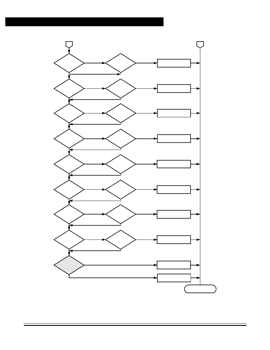
Technical Data
M68HC11K Family
128
Resets and Interrupts
MOTOROLA
Resets and Interrupts
Figure 5-9. Interrupt Priority Resolution (Sheet 2 of 2)
TOI = 1?
Y
N
Y
N
PAOVI = 1?
PAII = 1?
Y
N
SPIE = 1?
Y
N
Y
N
FLAG
Y
N
Y
N
FLAG
FLAG
Y
N
FLAGS
Y
N
PAIF = 1?
SPIF = 1? OR
TOF = 1?
PAOVF = 1
FETCH VECTOR
$FFDE, $FFDF
FETCH VECTOR
$FFDC, $FFDD
FETCH VECTOR
$FFDA, $FFDB
FETCH VECTOR
$FFD6, $FFD7
FETCH VECTOR
$FFD8, $FFD9
OC2I = 1?
Y
N
Y
N
OC3I = 1?
OC4I = 1?
Y
N
OC5I = 1?
Y
N
FLAG
Y
N
Y
N
FLAG
FLAG
Y
N
FLAG
Y
N
OC4F = 1?
OC5F = 1?
OC2F = 1?
OC3F = 1
FETCH VECTOR
$FFE6, $FFE7
FETCH VECTOR
$FFE4, $FFE5
FETCH VECTOR
$FFE2, $FFE3
FETCH VECTOR
$FFE0, $FFE1
MODF = 1?
INTERRUPT?
2A
2B
END
FETCH VECTOR
$FFF2, $FFF3
SCI
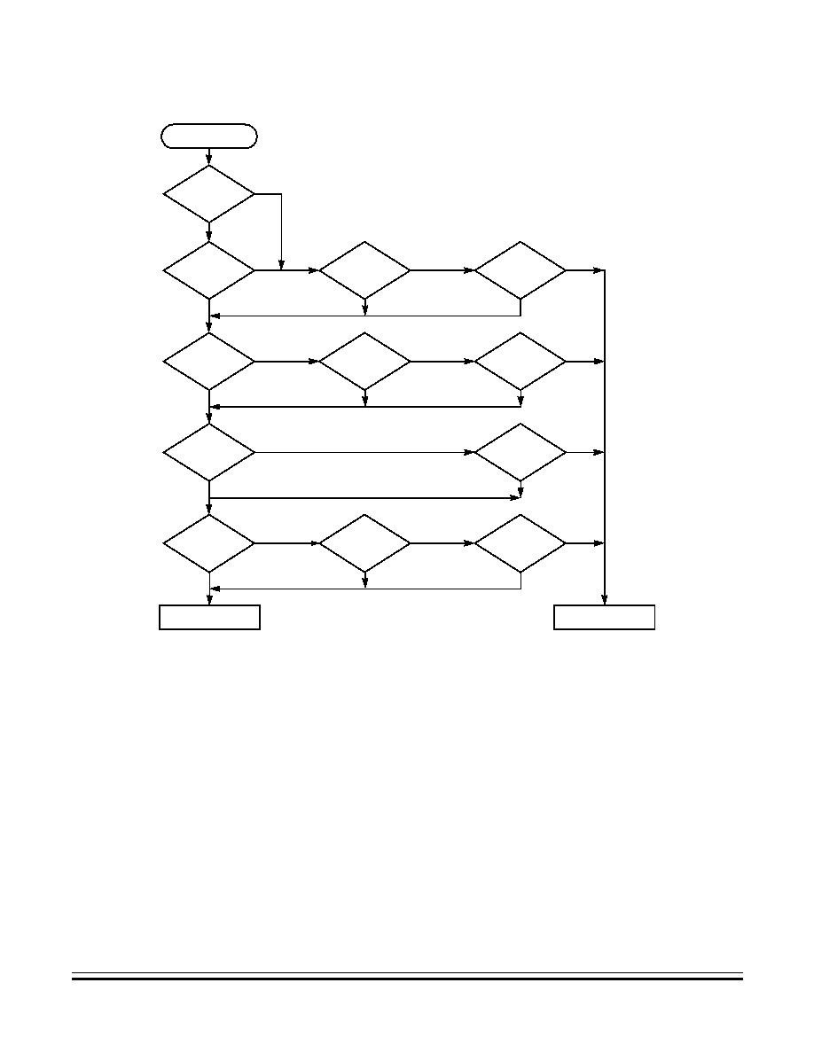
Resets and Interrupts
Low-Power Operation
M68HC11K Family
Technical Data
MOTOROLA
Resets and Interrupts
129
Figure 5-10. Interrupt Priority Resolution Within SCI System
5.8 Low-Power Operation
The MCU contains two software instructions, WAIT and STOP, to
reduce power consumption when processing is not required. Both
instructions suspend operation until a reset or interrupt occurs while
retaining register and RAM contents. The wait condition suspends
processing, reducing power consumption to an intermediate level. The
stop condition turns off all on-chip clocks as well and reduces power
consumption to an absolute minimum.
FLAG
Y
N
OR = 1?
Y
N
Y
N
TDRE = 1?
TC = 1?
Y
N
IDLE = 1?
Y
N
Y
N
Y
N
Y
N
ILIE = 1?
RIE = 1?
TIE = 1?
BEGIN
RE = 1?
Y
N
Y
N
TE = 1?
TCIE = 1?
Y
N
RE = 1?
Y
N
RDRF = 1?
VALID SCI REQUEST
NO
VALID SCI REQUEST

Technical Data
M68HC11K Family
130
Resets and Interrupts
MOTOROLA
Resets and Interrupts
5.8.1 Wait Mode
The WAI opcode places the MCU in the wait condition, during which the
CPU registers are stacked and CPU processing is suspended until a
qualified interrupt is detected. The interrupt can be an external IRQ, an
XIRQ, or any of the internally generated interrupts, such as the timer or
serial interrupts. The on-chip crystal oscillator remains active throughout
the wait standby period.
The reduction of power in the wait condition depends on how many
internal clock signals driving on-chip peripheral functions can be shut
down. The CPU is always shut down during WAIT. While in the wait
state, the address/data bus repeatedly runs read cycles to the address
where the CCR contents were stacked. The MCU leaves the wait state
when it senses any interrupt that has not been masked.
The free-running timer system is shut down only if maskable interrupts
are disabled (I bit is set) and the COP system is disabled (NOCOP is
set). Other systems can be shut down through the software-controlled
configuration control bits, including the SPI system (SPE control bit), the
SCI transmitter (TE bit), and the SCI receiver (RE bit). Net power
reduction in WAIT depends on which of these features is disabled.
5.8.2 Stop Mode
The STOP instruction halts all system clocks, including the crystal
oscillator, thereby minimizing power consumption. The S bit in the CCR
must be cleared to place the MCU in the stop condition; otherwise, the
stop opcode is treated as a no-operation (NOP). To exit STOP and
resume normal processing, a logic low level must be applied to one of
the external interrupt pins (IRQ or XIRQ) or to the RESET pin. A pending
edge-triggered IRQ can also bring the CPU out of stop.
Because all clocks are stopped in this mode, all internal peripheral
functions also stop. RAM and register contents are preserved as long as
V
DD
power is maintained. The CPU state and I/O pin levels are static and
are not altered by STOP, so the MCU resumes processing seamlessly
after the system is reactivated by an interrupt. However, if a reset is used
Resets and Interrupts
Low-Power Operation
M68HC11K Family
Technical Data
MOTOROLA
Resets and Interrupts
131
to restart the system, a normal reset sequence results and all pins and
registers are reinitialized.
To use the IRQ pin as a means of recovering from STOP, the I bit in the
CCR must be clear (IRQ not masked). The XIRQ pin can be used to
wake up the MCU from STOP regardless of the state of the X bit in the
CCR, although the state of this bit does affect the recovery sequence. If
X is clear (XIRQ not masked), the MCU executes a normal XIRQ service
routine. If X is set (XIRQ masked or inhibited), then processing continues
with the instruction that immediately follows the STOP instruction, and
no XIRQ interrupt service is requested or pending.
Executing a STOP instruction requires special consideration when the
clock monitor is enabled. Because the stop function halts all clocks, the
clock monitor function will generate a reset sequence if it is enabled at
the time the stop mode was initiated. To prevent this, clear the CME and
FCME bits in the OPTION register before executing a STOP instruction
to disable the clock monitor. After recovery from STOP, set the CME bit
to enable the clock monitor.
Systems using the internal oscillator require a delay after restart upon
leaving STOP to allow the oscillator to stabilize. If a stable external
oscillator is used, the DLY control bit in the OPTION register can be used
to bypass this startup delay (see
Figure 5-11
). Reset sets the DLY
control bit; it can be cleared during initialization. Do not use reset to
recover from STOP if the DLY is to be bypassed, since reset sets the
DLY bit again, causing the restart delay. This same delay will follow a
power-on reset, regardless of the state of the DLY control bit, but does
not apply to a reset while the clocks are running.
Address: $0039
Bit 7
6
5
4
3
2
1
Bit 0
Read:
ADPLE
DSEL
IRQE
(1)
DLY
(1)
CME
FCME
(1)
CR1
(1)
CR0
(1)
Write:
Reset:
0
0
0
1
0
0
0
0
1. Can be written only once in first 64 cycles out of reset in normal modes or at any time in
special modes
Figure 5-11. System Configuration Options Register (OPTION)

Technical Data
M68HC11K Family
132
Resets and Interrupts
MOTOROLA
Resets and Interrupts
DLY -- Enable Oscillator Startup Delay Bit
This bit is set during reset and can be written only once during the first
64 E-clock cycles after reset in normal modes. This bit can be used to
inhibit the oscillator startup delay after reset when using an external
clock source.
0 = No stabilization delay on exit from STOP
1 = Stabilization delay enabled on exit from STOP
5.8.3 Slow Mode
Slow mode is a software selectable feature on M68HC(7)11KS devices
that allows the user to connect, under software control, an extra
divide-by-16 between the oscillator and the internal clock. This feature
permits a slow down of all the internal operations reducing power
consumption.
When WAI is used for power reduction, the slow mode helps further
reduce the power. Control of slow mode is performed in the system
configuration options 3 register (OPT3). See
Figure 5-12
.
SM -- Slow-Mode Enable Bit
Read and write at any time
1 = When the SM bit is asserted, a 16-clock divider is connected
between the oscillator and the internal clock. This causes the
system clock to run 16 times slower than normal. All modules
of the MCU slow down, including the timer, SCI, SPI, and A/D.
It is also cleared in hardware when entering stop mode or when
reset, including POR, is asserted low.
0 = When the SM bit is negated, the divider is disconnected and the
system runs at normal bus speed.
Address: $002E
Bit 7
6
5
4
3
2
1
Bit 0
Read:
SM
Write:
Reset:
0
0
0
0
0
0
0
0
Figure 5-12. System Configuration Options 3 Register (OPT3)
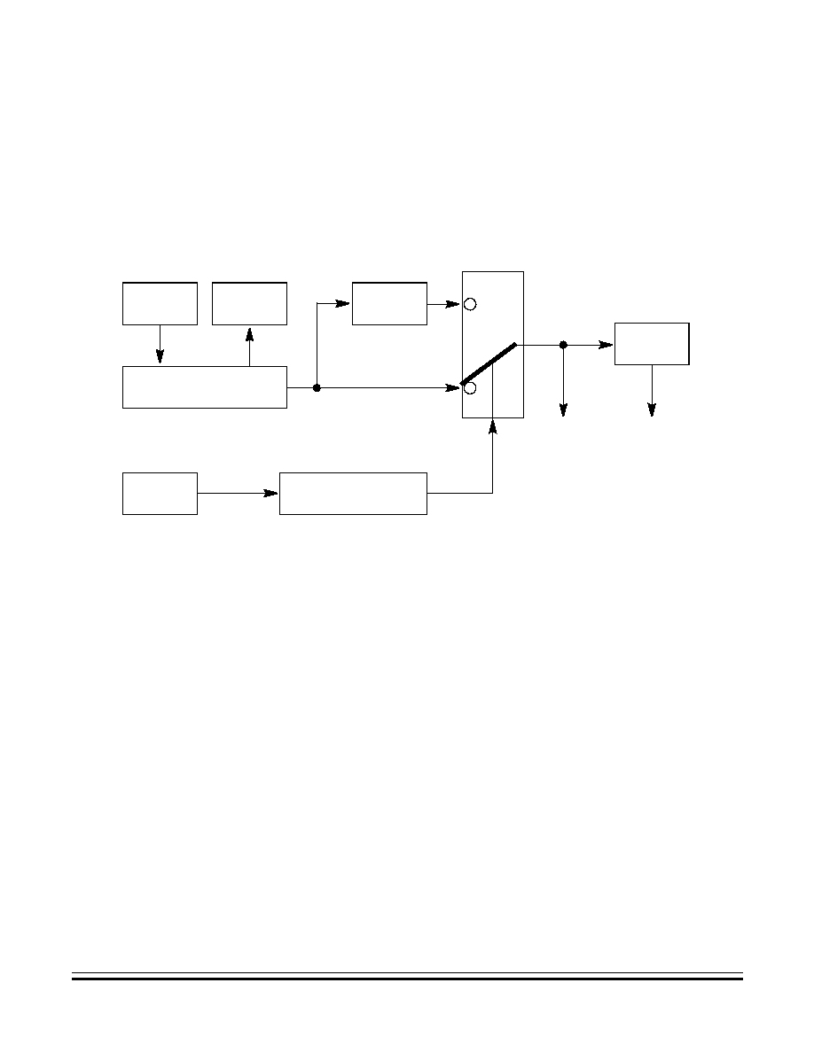
Resets and Interrupts
Low-Power Operation
M68HC11K Family
Technical Data
MOTOROLA
Resets and Interrupts
133
NOTE:
The slow mode function should not be enabled while using the A/D
converter or during an erase/program operation of the EEPROM, unless
the internal RC oscillator is turned on.
The clock monitor function should not be used if the resultant E clock will
be slower than 200 kHz.
Figure 5-13. Slow Mode Example for M68HC(7)11KS Devices Only
EXTAL
XTAL
OSCILLATOR
SM BIT
CONTROL LOGIC
SCI & XOUT
CIRCUITS
CPU & OTHER
MODULES
DIVIDE BY 4
MUX
XTAL
DIVIDE BY 16
IMMEDIATE
CHANGE
SM TO 1 REQUIRES LOW/HI/LOW
ON XTAL -- DIVIDE BY 16
RESETS -- MUX-OUT LOW
8 CYCLES -- DIVIDE BY 16 HIGH
8 CYCLES -- DIVIDE BY 16 LOW
MUX DIVIDE BY 16 TO SYSTEM

Technical Data
M68HC11K Family
134
Resets and Interrupts
MOTOROLA
Resets and Interrupts

M68HC11K Family
Technical Data
MOTOROLA
Parallel Input/Output
135
Technical Data -- M68HC11K Family
Section 6. Parallel Input/Output
6.1 Contents
6.2
Introduction . . . . . . . . . . . . . . . . . . . . . . . . . . . . . . . . . . . . . . . 136
6.3
Port A . . . . . . . . . . . . . . . . . . . . . . . . . . . . . . . . . . . . . . . . . . . 138
6.4
Port B . . . . . . . . . . . . . . . . . . . . . . . . . . . . . . . . . . . . . . . . . . . 139
6.5
Port C . . . . . . . . . . . . . . . . . . . . . . . . . . . . . . . . . . . . . . . . . . . 140
6.6
Port D . . . . . . . . . . . . . . . . . . . . . . . . . . . . . . . . . . . . . . . . . . . 142
6.7
Port E . . . . . . . . . . . . . . . . . . . . . . . . . . . . . . . . . . . . . . . . . . . 143
6.8
Port F . . . . . . . . . . . . . . . . . . . . . . . . . . . . . . . . . . . . . . . . . . . 144
6.9
Port G . . . . . . . . . . . . . . . . . . . . . . . . . . . . . . . . . . . . . . . . . . . 145
6.10
Port H . . . . . . . . . . . . . . . . . . . . . . . . . . . . . . . . . . . . . . . . . . . 146
6.11
Internal Pullup Resistors. . . . . . . . . . . . . . . . . . . . . . . . . . . . . 147
Technical Data
M68HC11K Family
136
Parallel Input/Output
MOTOROLA
Parallel Input/Output
6.2 Introduction
The M68HC11K series MCUs contain eight input/output (I/O) ports, A
through H. All ports can provide general-purpose I/O (GPIO) as well as
their specialized functions, as explained in
2.11 Port Signals
and
summarized in
Table 6-1
.
Each of the ports has an associated data register (PORTx). Each port,
except port E, also has an associated data direction register (DDRx).
When a port is configured for GPIO, its DDR determines whether port
pins function as inputs or outputs. A port's special functions override the
DDR when they are enabled.
Writes to any port, except port E, are stored in internal latches. The
latches drive the port pins only when they are configured as
general-purpose outputs.
When software reads a port pin configured for GPIO, the MCU returns
the physical pin level, not the port register value. This applies to both
inputs and outputs. The only exception applies to ports C and D in
wired-OR mode. When they are configured as outputs, a read returns
the pin driver levels.
Table 6-1. Port Configuration
Port
Input
Pins
Output
Pins
Bidirectional
Pins
Shared Functions
Port A
--
--
8
Timer
Port B
--
--
8
High-order address
Port C
--
--
8
Data bus
Port D
--
--
6
SCI and SPI
Port E
8
--
--
A/D converter
Port F
--
--
8
Low-order address
Port G
--
--
8
(1)
1. KS devices do not contain port G[6:0], so they have only one bidirectional pin on this port.
Memory expansion
Port H
--
--
8
(2)
2. KS devices do not contain port H[7:4], so they have only four bidirectional pins on this port.
Chip selects and PWM

Parallel Input/Output
Introduction
M68HC11K Family
Technical Data
MOTOROLA
Parallel Input/Output
137
Ports B, F, G, and H contain on-chip pullup devices which are enabled
by the port pullup assignment register (PPAR) described in
6.11 Internal
Pullup Resistors
.
At reset, the ports are configured as high-impedance GPIO inputs
(except for ports B, C, F, and port G pin 7 in expanded modes). The
contents of the data latches is undefined. If any of the bidirectional pins
are changed to outputs before writing to the associated data registers,
the undefined contents will be driven on the pins. This is indicated by the
letter U in the register descriptions that follow.
NOTE:
Throughout this manual, the registers are discussed by function. In the
event that not all bits in a register are referenced, the bits that are not
discussed are shaded.

Technical Data
M68HC11K Family
138
Parallel Input/Output
MOTOROLA
Parallel Input/Output
6.3 Port A
Port A provides the I/O lines for the timer functions and pulse
accumulator. The eight port A bits (PA[7:0]) are configured as
high-impedance general-purpose inputs out of reset. Writes to DDRA
can change any of the bits to outputs. Writes to timer registers enable
the various timer functions (see
Section 9. Timing System
).
DDA[7:0] -- Data Direction for Port A Bits
0 = Input
1 = Output
Address: $0000
Bit 7
6
5
4
3
2
1
Bit 0
Read:
PA7
PA6
PA5
PA4
PA3
PA2
PA1
PA0
Write:
Reset:
Undefined after reset
Alternate Pin Function:
PAI
OC2
OC3
OC4
IC4/OC5
IC1
IC2
IC3
And/or:
OC1
OC1
OC1
OC1
OC1
--
--
--
Figure 6-1. Port A Data Register (PORTA)
Address: $0001
Bit 7
6
5
4
3
2
1
Bit 0
Read:
DDA7
DDA6
DDA5
DDA4
DDA3
DDA2
DDA1
DDA0
Write:
Reset:
0
0
0
0
0
0
0
0
Figure 6-2. Port A Data Direction Register (DDRA)
Parallel Input/Output
Port B
M68HC11K Family
Technical Data
MOTOROLA
Parallel Input/Output
139
6.4 Port B
The state of port B (PB[7:0]) at reset is mode dependent. In single-chip
or bootstrap modes, port B pins are high-impedance inputs with
selectable internal pullup resistors (see
6.11 Internal Pullup
Resistors
). Writes to DDRB can change any of the bits to outputs. In
expanded or test modes, port B pins provide the high-order address
lines ADDR[15:8] for external memory devices.
DDB[7:0] -- Data Direction for Port B Bits
0 = Input
1 = Output
Address: $0004
Bit 7
6
5
4
3
2
1
Bit 0
Read:
PB7
PB6
PB5
PB4
PB3
PB2
PB1
PB0
Write:
Reset:
Undefined after reset
Single-Chip/Boot:
PB7I
PB6
PB5
PB4
PB3
PB2
PB1
PB0
Expanded/Test: ADDR15
ADDR14
ADDR13
ADDR12
ADDR11
ADDR10
ADDR9
ADDR8
Figure 6-3. Port B Data Register (PORTB)
Address: $0002
Bit 7
6
5
4
3
2
1
Bit 0
Read:
DDB7
DDB6
DDB5
DDB4
DDB3
DDB2
DDB1
DDB0
Write:
Reset:
0
0
0
0
0
0
0
0
Figure 6-4. Port B Data Direction Register (DDRB)

Technical Data
M68HC11K Family
140
Parallel Input/Output
MOTOROLA
Parallel Input/Output
6.5 Port C
The state of port C at reset is mode dependent. In single-chip or
bootstrap modes, port C pins (PC[7:0]) are high-impedance inputs.
Writes to DDRC can change any of the bits to outputs. In expanded or
test modes, port C pins provide the data lines (DATA[7:0]) for external
memory devices. The MCU's internal data bus can also be driven on port
C by setting the IRVNE bit in the system configuration options register
(OPT2). See
Figure 6-7
.
When port C functions as GPIO (single-chip mode), it can be configured
for wired-OR operation by setting the CWOM bit in the OPT2 register.
This disables port C's P-channel drivers, effectively generating
open-drain-type outputs. To output a logic 0 on a wired-OR pin, the MCU
turns on its N-channel driver. To generate a logic 1, both P- and
N-channel drivers are turned off, presenting a high-impedance state
which requires an external pullup resistor to apply the appropriate
voltage level.
Address: $0006
Bit 7
6
5
4
3
2
1
Bit 0
Read:
PC7
PC6
PC5
PC4
PC3
PC2
PC1
PC0
Write:
Reset:
Undefined after reset
Single-Chip/Boot:
PC7I
PC6
PC5
PC4
PC3
PC2
PC1
PC0
Expanded/Test:
DATA7
DATA6
DATA5
DATA4
DATA3
DATA2
DATA1
DATA0
Figure 6-5. Port C Data Register (PORTC)
Parallel Input/Output
Port C
M68HC11K Family
Technical Data
MOTOROLA
Parallel Input/Output
141
DDC[7:0] -- Data Direction for Port C Bits
0 = Input
1 = Output
CWOM -- Port C Wired-OR Mode Bit
0 = Port C operates normally.
1 = Port C outputs are open drain.
IRVNE -- Internal Read Visibility/Not E Bit
In expanded modes, setting this bit drives MCU's internal data bus on
port C.
0 = No internal read visibility on external data bus
1 = Data from internal reads is driven on port C.
In single-chip modes, setting this bit inhibits the E clock driver, and the
E pin is pulled low
0 = E clock drives the E pin.
1 = E pin is driven low.
NOTE:
IRVNE can be written only once after reset. The default value of IRVNE
after reset is low.
Address: $0007
Bit 7
6
5
4
3
2
1
Bit 0
Read:
DDC7
DDC6
DDC5
DDC4
DDC3
DDC2
DDC1
DDC0
Write:
Reset:
0
0
0
0
0
0
0
0
Figure 6-6. Port C Data Direction Register (DDRC)
Address: $0038
Bit 7
6
5
4
3
2
1
Bit 0
Read:
LIRDV
CWOM
STRCH
(1)
IRVNE
LSBF
SPR2
XDV1
XDV0
Write:
Reset:
0
0
0
--
0
0
0
0
1. Not available on KS devices
Figure 6-7. System Configuration Options 2 Register (OPT2)
Technical Data
M68HC11K Family
142
Parallel Input/Output
MOTOROLA
Parallel Input/Output
6.6 Port D
The six port D bits, PD[5:0] function as the serial communication
interface (see
Section 7. Serial Communications Interface (SCI)
) and
the serial peripheral interface (see
Section 8. Serial Peripheral
Interface (SPI)
) when these functions are enabled by software. They are
high-impedance general-purpose inputs out of reset; DDRD can be used
to change any of the pins to outputs.
DDD[5:0] -- Data Direction for Port D Bits
0 = Input
1 = Output
Address: $0008
Bit 7
6
5
4
3
2
1
Bit 0
Read:
0
0
PD5
PD4
PD3
PD2
PD1
PD0
Write:
Reset:
0
0
U
U
U
U
U
U
Alternate Pin Function:
--
--
SS
SCK
MOSI
MISO
TxD
RxD
U = Undefined
Figure 6-8. Port D Data Register (PORTD)
Address: $0009
Bit 7
6
5
4
3
2
1
Bit 0
Read:
0
0
DDD5
DDD4
DDD3
DDD2
DDD1
DDD0
Write:
Reset:
0
0
0
0
0
0
0
0
Figure 6-9. Port D Data Direction Register (DDRD)

Parallel Input/Output
Port E
M68HC11K Family
Technical Data
MOTOROLA
Parallel Input/Output
143
6.7 Port E
Port E, PE[7:0], is the only port that functions as input only, and its pins
are configured as high-impedance inputs out of reset. It also serves as
the analog input for the analog-to-digital converter when this function is
enabled by software (see
Section 10. Analog-to-Digital (A/D)
Converter
).
NOTE:
PORT E should not be read during the sample portion of an A/D
conversion.
Address: $000A
Bit 7
6
5
4
3
2
1
Bit 0
Read:
PE7
PE6
PE5
PE4
PE3
PE2
PD1
PD0
Write:
Reset:
Undefined after reset
Alternate Pin Function:
AN7
AN6
AN5
AN4
AN3
AN2
AN1
AN0
Figure 6-10. Port E Data Register (PORTE)

Technical Data
M68HC11K Family
144
Parallel Input/Output
MOTOROLA
Parallel Input/Output
6.8 Port F
The state of port F (PF[7:0]) at reset is mode dependent. In single-chip
or bootstrap modes, port F pins are high-impedance inputs with
selectable internal pullup resistors (see
6.11 Internal Pullup
Resistors
). Writes to DDRF can change any of the bits to outputs. In
expanded or test modes, port F pins provide low-order address lines,
ADDR[7:0], for external memory devices.
DDF[7:0] -- Data Direction for Port F Bits
0 = Input
1 = Output
Address: $0005
Bit 7
6
5
4
3
2
1
Bit 0
Read:
PF7
PF6
PF5
PF4
PF3
PF2
PF1
PF0
Write:
Reset:
Undefined after reset
Single-Chip/Boot:
PF7
PF6
PF5
PF4
PF3
PF2
PF1
PF0
Expanded/Test:
AN7
AN6
AN5
AN4
AN3
AN2
AN1
AN0
Figure 6-11. Port F Data Register (PORTF)
Address: $0003
Bit 7
6
5
4
3
2
1
Bit 0
Read:
DDF7
DDF6
DDF5
DDF4
DDF3
DDF2
DDF1
DDF0
Write:
Reset:
0
0
0
0
0
0
0
0
Figure 6-12. Port F Data Direction Register (DDRF)
Parallel Input/Output
Port G
M68HC11K Family
Technical Data
MOTOROLA
Parallel Input/Output
145
6.9 Port G
The state of port G pin 7 (PG7) at reset is mode dependent. In
single-chip or bootstrap modes, it is a high-impedance input; its data
direction can be changed through DDRG. In expanded and special test
modes, PG7 functions as the R/W line to control the direction of data flow
between the MCU and external memory devices.
Port G pins (PG[6:0]) reset to high-impedance inputs in any mode. Data
direction can be changed through DDRG. Port G bits [5:0] can serve as
memory expansion address lines (see
11.3 Memory Expansion
) in
expanded and special test modes. M68HC11KS devices do not contain
these pins.
All eight port G pins have selectable internal pullup resistors (see
6.11
Internal Pullup Resistors
).
DDG[7:0] -- Data Direction for Port G Bits
0 = Input
1 = Output
Address: $007E
Bit 7
6
5
4
3
2
1
Bit 0
Read:
PG7
PG6
(1)
PG5
(1)
PG4
(1)
PG3
(1)
PG2
(1)
PG1
(1)
PG0
(1)
Write:
Reset:
0
0
0
0
0
0
0
0
Alternate Pin Function:
R/W
--
XA18
XA17
XA16
XA15
XA14
XA13
1. Not available on KS devices
Figure 6-13. Port G Data Register (PORTG)
Address: $007F
Bit 7
6
5
4
3
2
1
Bit 0
Read:
DDG7
DDG6
(1)
DDG5
(1)
DDG4
(1)
DDG3
(1)
DDG2
(1)
DDG1
(1)
DDG0
(1)
Write:
Reset:
0
0
0
0
0
0
0
0
1. Not available on KS devices
Figure 6-14. Port G Data Direction Register (DDRG)

Technical Data
M68HC11K Family
146
Parallel Input/Output
MOTOROLA
Parallel Input/Output
6.10 Port H
The state of port H pin 7 (PH7) at reset is mode dependent. In single-chip
or bootstrap modes, it is a high-impedance input; its data direction can
be changed through DDRH. In expanded and special test modes PH7 is
the program chip select line, CSPROG at reset, but can be reconfigured
for GPIO (see
11.4 Chip Selects
).
Port H pins (PH[6:0]) reset to high-impedance inputs in any mode. Data
direction can be changed through DDRH. Except for the M68HC11KS
devices, bits 6:4 can serve as chip select lines in expanded and special
test modes (see
11.4 Chip Selects
). Pins 3:0 can be configured as
pulse-width modulator outputs (see
9.9 Pulse-Width Modulator
(PWM)
) in any mode.
All eight port H pins have selectable internal pullup resistors (see
6.11 Internal Pullup Resistors
).
DDH[7:0] -- Data Direction for Port H Bits
0 = Input
1 = Output
Address: $007C
Bit 7
6
5
4
3
2
1
Bit 0
Read:
PH7
(1)
PH6
(1)
PH5
(1)
PH4
(1)
PH3
PH2
PH1
PH0
Write:
Reset:
0
0
0
0
0
0
0
0
Alternate Pin Function: CSPROG
CSPG2
CSPG1
CSIO
PW4
PS3
PS2
PS1
1. Not available on KS devices
Figure 6-15. Port H Data Register (PORTH)
Address: $007D
Bit 7
6
5
4
3
2
1
Bit 0
Read:
DDH7
(1)
DDH6
(1)
DDH5
(1)
DDH4
(1)
DDH3
DDH2
DDH1
DDH0
Write:
Reset:
0
0
0
0
0
0
0
0
1. Not available on KS devices
Figure 6-16. Port H Data Direction Register (DDRH)

Parallel Input/Output
Internal Pullup Resistors
M68HC11K Family
Technical Data
MOTOROLA
Parallel Input/Output
147
6.11 Internal Pullup Resistors
M68HC11KS series devices contain selectable internal pullup resistors
for ports B, F, G, and H. The resistors for each port are enabled by
setting the corresponding bit in the PPAR register. PPAR itself must be
enabled by setting the PAREN bit in the system configuration register
(CONFIG). Refer to
Figure 6-17
and
Figure 6-18
.
xPPUE -- Port x Pin Pullup Enable Bits
Only active when enabled by the PAREN bit in the CONFIG register
0 = Port x pin on-chip pullup devices disabled
1 = Port x pin on-chip pullup devices enabled
NOTE:
FPPUE and BPPUE do not apply in expanded mode because port F and
B are address outputs.
NOTE:
CONFIG is writable once in normal modes and writable at any time in
special modes.
PAREN -- Pullup Assignment Register Enable Bit
0 = PPAR register disabled
1 = PPAR register enabled; pullups can be enabled through PPAR
Address: $002C
Bit 7
6
5
4
3
2
1
Bit 0
Read:
0
0
0
0
HPPUE
GPPUE
FPPUE
BPPUE
Write:
Reset:
0
0
0
0
1
1
1
1
Figure 6-17. Port Pullup Assignment Register (PPAR)
Address: $003F
Bit 7
6
5
4
3
2
1
Bit 0
Read:
ROMAD
1
CLKX
PAREN
NOSEC
NOCOP
ROMON
EEON
Write:
Reset:
--
1
--
--
1
--
--
--
Figure 6-18. System Configuration Register (CONFIG)

Technical Data
M68HC11K Family
148
Parallel Input/Output
MOTOROLA
Parallel Input/Output

M68HC11K Family
Technical Data
MOTOROLA
Serial Communications Interface (SCI)
149
Technical Data -- M68HC11K Family
Section 7. Serial Communications Interface (SCI)
7.1 Contents
7.2
Introduction . . . . . . . . . . . . . . . . . . . . . . . . . . . . . . . . . . . . . . . 149
7.3
Data Format . . . . . . . . . . . . . . . . . . . . . . . . . . . . . . . . . . . . . . 150
7.4
Transmit Operation . . . . . . . . . . . . . . . . . . . . . . . . . . . . . . . . .151
7.5
Receive Operation . . . . . . . . . . . . . . . . . . . . . . . . . . . . . . . . . 153
7.6
Wakeup Feature . . . . . . . . . . . . . . . . . . . . . . . . . . . . . . . . . . . 156
7.7
Short Mode Idle Line Detection . . . . . . . . . . . . . . . . . . . . . . .157
7.8
Baud Rate Selection . . . . . . . . . . . . . . . . . . . . . . . . . . . . . . . . 157
7.9
SCI Registers . . . . . . . . . . . . . . . . . . . . . . . . . . . . . . . . . . . . .158
7.9.1
SCI Baud Rate Control Register . . . . . . . . . . . . . . . . . . . . 158
7.9.2
Serial Communications Control Register 1 . . . . . . . . . . . . 160
7.9.3
Serial Communications Control Register 2 . . . . . . . . . . . . 161
7.9.4
Serial Communication Status Register 1 . . . . . . . . . . . . . . 162
7.9.5
Serial Communication Status Register 2 . . . . . . . . . . . . . . 164
7.9.6
Serial Communications Data Register . . . . . . . . . . . . . . . . 165
7.2 Introduction
The serial communications interface (SCI) is a universal asynchronous
receiver transmitter (UART) employing a standard non-return-to-zero
(NRZ) format. Several baud rates are available. The SCI transmitter and
receiver are independent, but they use the same data format and baud
rate.
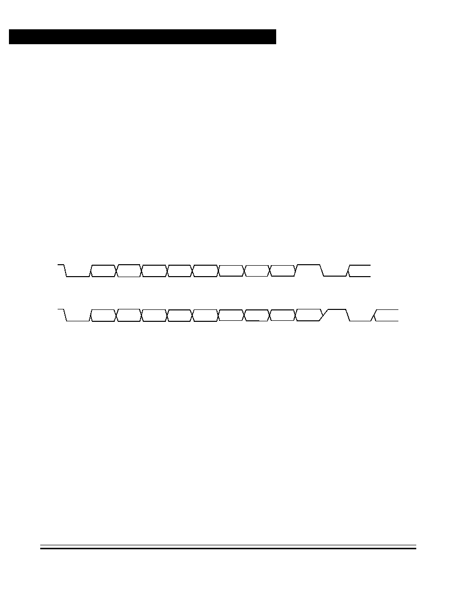
Technical Data
M68HC11K Family
150
Serial Communications Interface (SCI)
MOTOROLA
Serial Communications Interface (SCI)
The M68HC11K series offers several enhancements to the basic
MC68HC11 SCI, including:
�
13-bit modulus prescaler in the baud generator
�
Receiver-active flag
�
Transmitter and receiver hardware parity
�
Accelerated idle line detection
7.3 Data Format
The SCI uses the standard non-return to zero mark/space data format
illustrated in
Figure 7-1
.
Figure 7-1. SCI Data Formats
Data is transmitted in frames consisting of a start bit, a word of eight or
nine data bits, and a stop bit. The step-by-step transmission procedure
is:
1. The transmission line is idle before a message is transmitted. This
means that the line is in a logic 1 state for at least one frame time.
2. A start bit, logic 0, is transmitted, indicating the start of a frame.
3. An 8-bit or 9-bit word is transmitted, least significant bit (LSB) first.
4. A stop bit, logic 1, is transmitted to indicate the end of a frame.
5. An optional number of breaks can be transmitted. A break is the
transmission of a logic low state for one frame time. After the last
break character is sent, the line goes high for at least one bit time.
START
BIT
BIT 0
BIT 2
BIT 3
BIT 1
BIT 4
BIT5
BIT7
BIT6
STOP
BIT
NEXT
START
BIT
NEXT
START
BIT
STOP
BIT
PARITY
OR DATA
BIT
BIT 8
BIT 7
BIT 6
BIT 5
BIT 4
BIT 3
BIT 2
BIT 1
BIT 0
START
BIT
9-BIT DATA FORMAT
(BIT MIN SCC1 SET)
8-BIT DATA FORMAT
(BIT MIN SCC1 CLEAR)

Serial Communications Interface (SCI)
Transmit Operation
M68HC11K Family
Technical Data
MOTOROLA
Serial Communications Interface (SCI)
151
6. Steps 2-5 are repeated until the entire message is sent.
7. The line returns to idle status.
7.4 Transmit Operation
Transmission starts by writing a data character to the 2-byte SCI data
register (SCDRH and SCDRL). The MCU parallel-loads the character
into a serial shift register which shifts the data out on the transmission
pin. This double-buffered operation allows transmission of the current
character while the MCU loads the next one. The output of the serial shift
register drives the TxD pin as long as the transmit enable (TE) bit of
serial communication control register 2 (SCCR2) is set.
Two flags in serial communication status register 1 (SCSR1) alert the
MCU of transmission status. The TDRE (transmit data register empty)
flag is set when the SCDR loads its contents into the shift register; this
flag can generate an interrupt if the TIE (transmit interrupt enable) bit in
SCCR2 is set. The TC (transmit complete) flag is set when transmission
is complete (line idle); this can also generate an interrupt if the TCIE
(transmit complete interrupt enable) bit in SCSR1 is set. The TDRE and
TC flags are normally set when software sets the TE bit to enable the
transmitter. See
Figure 5-10. Interrupt Priority Resolution Within SCI
System
for a flow diagram of SCI interrupts.
If interrupts are not enabled, the status flags can be read by software
(polled) to determine when the corresponding conditions exist. Status
flags are set automatically by hardware logic conditions, but must be
cleared by software. The software clearing sequence for these flags is
automatic. Functions that are normally performed in response to the
status flags also satisfy the conditions of the clearing sequence.
When software clears the TE bit, the TxD pin reverts to its
general-purpose I/O function (PD1). The transmitter completes
transmission of a character in progress before actually shutting down;
other characters waiting in the transmit queue are lost. The TC and
TDRE flags are set at the completion of this last character, even though
TE has been disabled. Only an MCU reset can abort transmission in
midcharacter.
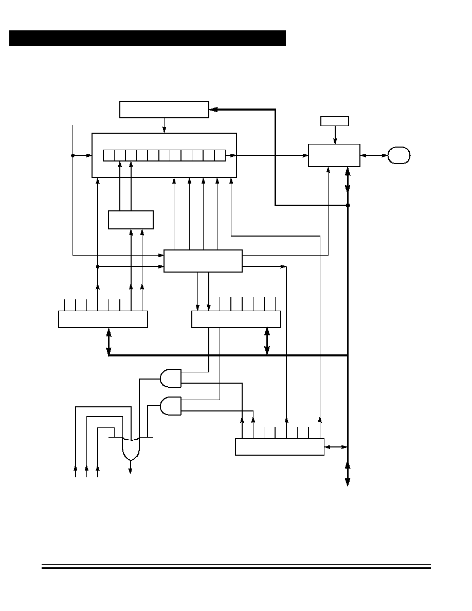
Technical Data
M68HC11K Family
152
Serial Communications Interface (SCI)
MOTOROLA
Serial Communications Interface (SCI)
Figure 7-2
is a block diagram of the SCI transmitter.
Figure 7-2. SCI Transmitter Block Diagram
TC
TDRE
SCSR1
SCI STATUS 1
SCCR2
SCI CONTROL 2
TRANSMITTER
CONTROL LOGIC
TCIE
TC
TIE
TDRE
SCI Rx
REQUESTS
SCI INTERRUPT
REQUEST
INTERNAL
DATA BUS
PIN BUFFER
AND CONTROL
H
10 (11) -- BIT Tx SHIFT REGISTER
DDD1
(1)
SCDR Tx BUFFER
T
R
AN
SF
ER
T
x
B
U
F
F
E
R
S
H
I
F
T
EN
ABLE
J
A
M
EN
ABLE
PR
EA
M
B
LE
--
JA
M
1
s
BR
EA
K
--
JA
M
0
s
WRITE ONLY
FORCE PIN
DIRECTION (OUT)
SI
Z
E
8/
9
M
SCCR1
SCI CONTROL 1
TRANSMITTER
BAUD RATE
CLOCK
PARITY
GENERATOR
PE
PT
TI
E
TC
IE
TI
E
TE
SBK
8
7
6
5
4
3
2
1
0
L
PD1
TxD
Note 1. Data direction register for port D
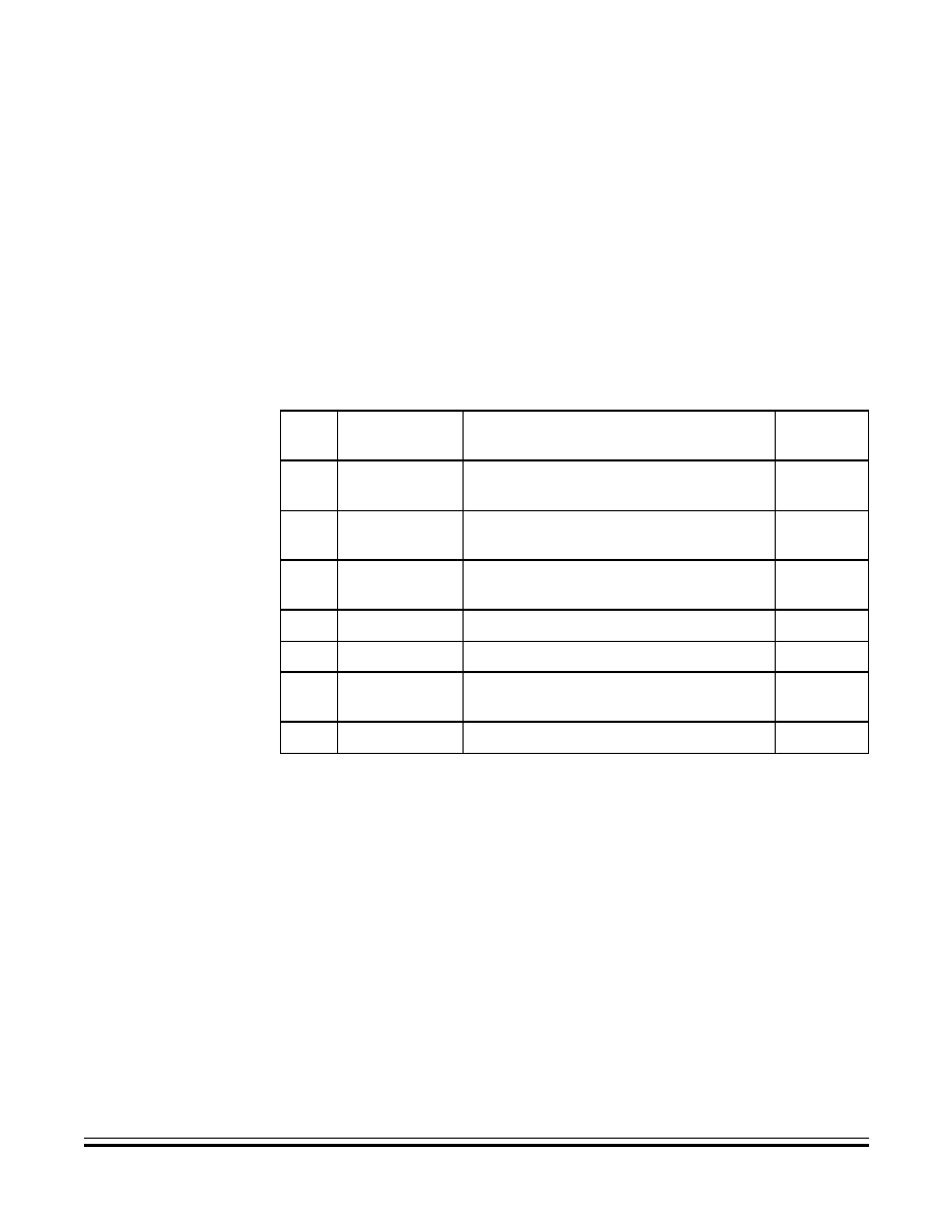
Serial Communications Interface (SCI)
Receive Operation
M68HC11K Family
Technical Data
MOTOROLA
Serial Communications Interface (SCI)
153
7.5 Receive Operation
During receive operations, data from the TxD pin is shifted into the serial
shift register. A completed word is parallel-loaded to a receive data
register (RDR), which can be read through SCDRH/L. This
double-buffered operation allows reception of the current character while
the MCU reads the previous character.
The SCI receiver has seven status flags, summarized in
Table 7-1
.
Three of the flags can generate interrupt requests if the corresponding
enable bits in SCCR2 are set. The status flags are set by the SCI logic
in response to specific conditions in the receiver. These flags can be
read (polled) at any time by software. Each bit except RAF is cleared by
reading SCSR1 and SCDR sequentially.
�
The receive data register full (RDRF) flag is set when the last bit
of a character is received and data is transferred from the shift
register to the RDR.
�
The IDLE flag is set after a transition on the RxD line from an
active state to an idle state. This prevents repeated interrupts
during the time RxD remains idle.
Table 7-1. SCI Receiver Flags
Flag
Name
Set When
Interrupt
Enable Bit
RDRF
Receive data
register full
Character transferred from shift register
to RDR
RIE
IDLE
Idle-line
detected
Active transmit line goes idle
ILIE
OR
Overrun error
Character ready for RDR while previous
character unread
RIE
NF
Noise error
Samples of data bit not unanimous
--
FE
Frame error
0 detected where stop bit expected
--
PF
Parity error
Calculated parity does not match data
parity bit
--
RAF
Receiver active
A character is being received
--

Technical Data
M68HC11K Family
154
Serial Communications Interface (SCI)
MOTOROLA
Serial Communications Interface (SCI)
�
The overrun error (OR) flag is set instead of the RDRF bit when
the next byte is ready to be transferred from the receive shift
register to the RDR and the RDR is already full. The data in the
shift register is lost and the data that was already in RDR is not
disturbed.
�
The noise flag (NF) is set if there is noise on any of the received
bits, including the start and stop bits. The data recovery circuit
takes three samples of each bit and indicates noise if any set of
three samples is not unanimous. NF is not set until the entire
character is received and transferred to the RDR, when RDRF is
set.
�
The framing error (FE) flag is set when no stop bit is detected in
the received data character. FE is set at the same time as RDRF.
If the byte received causes both framing and overrun errors, the
processor only recognizes the overrun error. The framing error
flag inhibits further data transfer into the RDR until the flag is
cleared.
�
The parity error (PE) flag indicates that the parity bit of a received
character does not match the parity calculated by hardware.
�
The receiver active flag (RAF) is a read-only bit that is set during
data reception and cleared when the line goes idle. This is the only
flag cleared by hardware.
Figure 7-3
is a block diagram of the SCI receiver.
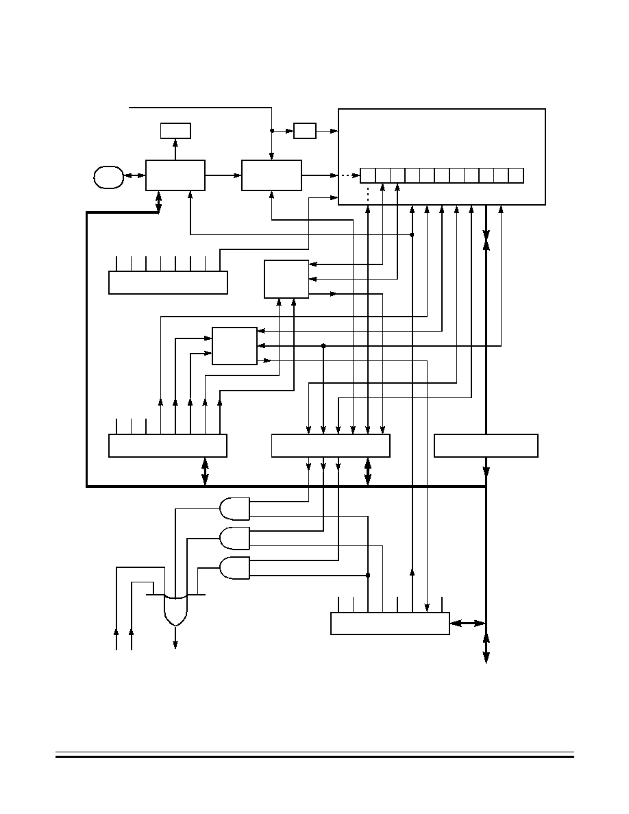
Serial Communications Interface (SCI)
Receive Operation
M68HC11K Family
Technical Data
MOTOROLA
Serial Communications Interface (SCI)
155
Figure 7-3. SCI Receiver Block Diagram
SCSR1
SCI STATUS 1
SCCR2
SCI CONTROL 2
SCI Rx
REQUESTS
SCI INTERRUPT
REQUEST
INTERNAL
DATA BUS
H
10 (11) - BIT
M
SCCR1
SCI CONTROL 1
RECEIVER
BAUD RATE
CLOCK
PARITY
DETECT
PE
PT
RI
E
IL
IE
8
7
6
5
4
3
2
1
0
L
PD0
RxD
SCDR
Rx BUFFER
Tx SHIFT REGISTER
DDD0
(1)
PIN BUFFER
AND CONTROL
DATA
RECOVERY
�
16
ST
O
P
ST
AR
T
MSB
ALL
ONES
RE
WAKEUP
LOGIC
SCSR2
SCI STATUS 2
RA
F
RDR
F
IDL
E
OR
NF
FE
PF
RWU
DISABLE
DRIVER
WA
K
E
IL
T
(READ ONLY)
RDRF
RIE
IDLE
ILIE
OR
RIE
Note 1. Data direction register for port D

Technical Data
M68HC11K Family
156
Serial Communications Interface (SCI)
MOTOROLA
Serial Communications Interface (SCI)
7.6 Wakeup Feature
The wakeup feature reduces SCI service overhead in multiple receiver
systems. If a system generates address information at the beginning of
every message, each receiver can determine whether or not it is the
intended recipient of a message by evaluating the first character(s)
through software.
If the message is intended for a different receiver, the SCI can be placed
in a sleep mode so that the rest of the message will not generate
requests for service. It does this by setting the RWU (receiver wakeup)
bit in SCI control register 2 (SCCR2), which inhibits all receiver-related
status flags (RDRF, IDLE, OR, NF, FE, PF, and RAF). A new message
clears the receiver's RWU bit, enabling it to evaluate the new address
information. Although RWU can be cleared by a software write to
SCCR2, this is rarely done because hardware clears RWU
automatically.
Two methods of wakeup are available:
�
Idle line wakeup -- A sleeping receiver wakes up as soon as the
RxD line becomes idle (for example, in a logic 1 state for at least
one frame time). A system using this type of wakeup must provide
at least one character time of idle between messages to wake up
sleeping receivers and must not allow any idle time between
characters within a message.
�
Address mark wakeup -- Uses the most significant bit (MSB) to
distinguish address characters (MSB = 1) from data characters
(MSB = 0). A sleeping receiver wakes up whenever it receives an
address character. Unlike the idle line method, address mark
wakeup allows idle periods within messages and does not require
idle time between messages. However, message processing is
less efficient because the start bit of each character must be
evaluated.
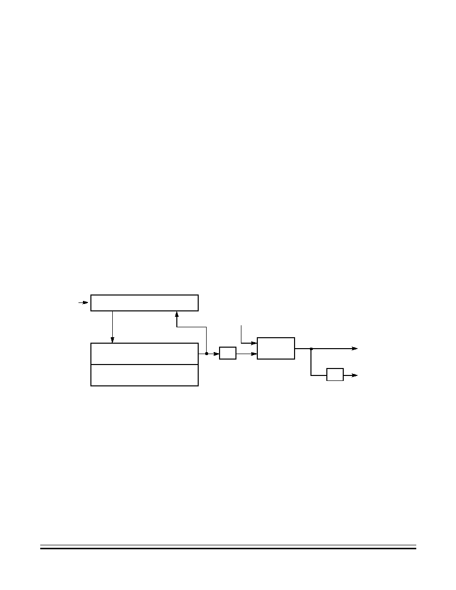
Serial Communications Interface (SCI)
Short Mode Idle Line Detection
M68HC11K Family
Technical Data
MOTOROLA
Serial Communications Interface (SCI)
157
7.7 Short Mode Idle Line Detection
This feature can increase system communication speed by reducing the
amount of time between messages. Setting the ILT bit in SCCR1 allows
the SCI receiver to detect the consecutive 1s of an idle period before the
stop bit of an incoming character is received. If the last few bits of the
character are 1s, they are counted as the first high bits in the frame of 1s
comprising the idle period following the character.
NOTE:
Extra care may be needed to prevent premature detection of an idle line
condition.
7.8 Baud Rate Selection
The baud rate generator for the SCI includes a 13-bit modulus prescaler
driven by the system crystal clock (EXTAL). Writing to the SCI baud rate
register (SCBDH/L) selects the prescaler value. See
Figure 7-4
.
Figure 7-4. SCI Baud Generator Circuit Diagram
13-BIT COUNTER
EXTAL
13-BIT COMPARE
SCBDH/L SCI BAUD RATE
�
2
INTERNAL
PHASE 2
CLOCK
SYNCH
�
16
TRANSMITTER
BAUD RATE
CLOCK
RECEIVER
BAUD RATE
CLOCK
RESET
CONTROL

Technical Data
M68HC11K Family
158
Serial Communications Interface (SCI)
MOTOROLA
Serial Communications Interface (SCI)
7.9 SCI Registers
The six addressable registers in the SCI are:
�
SCI baud rate control register (SCBDH and SCBDL)
�
Serial communications control register 1 (SCCR1)
�
Serial communications control register 2 (SCCR2)
�
Serial communication status register 1 (SCSR1)
�
Serial communication status register 2 (SCSR2)
�
Serial communications data register (SCDRH and SCDRL)
NOTE:
Throughout this manual, the registers are discussed by function. In the
event that not all bits in a register are referenced, the bits that are not
discussed are shaded.
7.9.1 SCI Baud Rate Control Register
This register selects the 13-bit divisor shown in
Figure 7-4
to generate
the SCI baud rate. (See
Table 7-2
.) Normally, this register is written once
during initialization, but it can be changed at any time.
Address: $0070
Bit 7
6
5
4
3
2
1
Bit 0
Read:
BTST
BSPL
0
SBR12
SBR11
SBR10
SBR9
SBR8
Write:
Reset:
0
0
0
0
0
U
U
U
U = Undefined
Figure 7-5. SCI Baud Rate Control Register High (SCBDH)
Address: $0071
Bit 7
6
5
4
3
2
1
Bit 0
Read:
SBR7
SBR6
SBR5
SBR4
SBR3
SBR2
SBR1
SBR0
Write:
Reset:
0
0
0
0
0
U
U
U
U = Undefined
Figure 7-6. SCI Baud Rate Control Register Low (SCBDL)
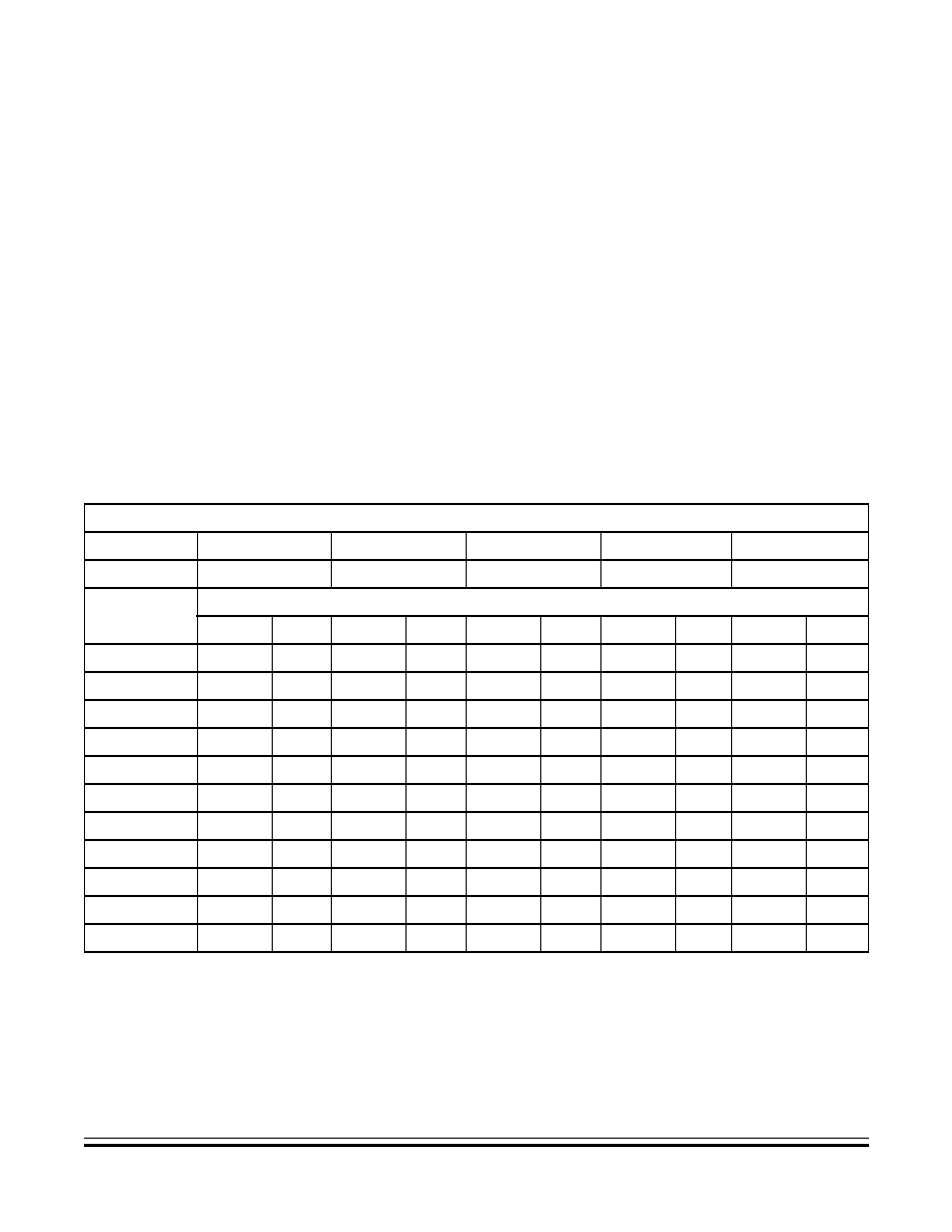
Serial Communications Interface (SCI)
SCI Registers
M68HC11K Family
Technical Data
MOTOROLA
Serial Communications Interface (SCI)
159
BTST -- Baud Register Test Bit
BTST is for factory use only and is only accessible in special test
mode.
BSPL -- Baud Rate Counter Split Bit
BSOK is for factory use only and is only accessible in special test
mode.
SBR[12:0] -- SCI Baud Rate Select Bits
These bits represent the value BR in:
SCI baud rate control
register value = (EXTAL/32)/target baud rate
Table 7-2. SCI+ Baud Rates
EXTAL Frequencies
EXTAL Freq.
8.0 MHz
12.0 MHz
16.0 MHz
20.0 MHz
24.0 MHz
E Clock Freq.
2.0 MHz
3.0 MHz
4.0 MHz
5.0 MHz
6.0 MHz
Target
Baud Rate
SCI Baud Rate Control Register Values
Decimal
Hex
Decimal
Hex
Decimal
Hex
Decimal
Hex
Decimal
Hex
110 baud
2273
$08E1
3409
$0D51
4545
$11C1
5682
$1632
6818
$1AA2
150 baud
1667
$0683
2500
$09C4
3333
$0D05
4167
$1047
5000
$1388
300 baud
833
$0341
1250
$04E2
1667
$0683
2083
$0823
2500
$09C4
600 baud
417
$01A1
625
$0271
833
$0341
1042
$0412
1250
$04E2
1200 baud
208
$00D0
313
$0139
417
$01A1
521
$0209
625
$0271
2400 baud
104
$0068
156
$009C
208
$00D0
260
$0104
313
$0139
4800 baud
52
$0034
78
$004E
104
$0068
130
$0082
156
$009C
9600 baud
26
$001A
39
$0027
52
$0034
65
$0041
78
$004E
19200 baud
13
$000D
20
$0014
26
$001A
33
$0021
39
$0027
38400 baud
--
--
--
--
13
$000D
16
$0010
20
$0014
76800 baud
--
--
--
--
--
--
8
$0008
10
$000A
Technical Data
M68HC11K Family
160
Serial Communications Interface (SCI)
MOTOROLA
Serial Communications Interface (SCI)
7.9.2 Serial Communications Control Register 1
LOOPS -- SCI Loop Mode Enable Bit
Both the transmitter and receiver must be enabled to use the loop
mode. When the loop mode is enabled, the TxD pin is driven high (idle
line state) if the transmitter is enabled.
0 = SCI transmit and receive operate normally.
1 = SCI transmit and receive are disconnected from TxD and RxD
pins, and transmitter output is fed back into the receiver input.
WOMS -- Wired-OR Mode for SCI Pins PD[1:0] Bits
See also
8.6.1 Serial Peripheral Control Register
for a description
of the DWOM (port D wired-OR mode) bit in the serial peripheral
control register (SPCR).
0 = TxD and RxD operate normally.
1 = TxD and RxD are open drains if operating as outputs.
M -- Mode (SCI Word Size) Bit
0 = Start bit, 8 data bits, 1 stop bit
1 = Start bit, 9 data bits, 1 stop bit
WAKE -- Wakeup Mode Bit
0 = Wake up by idle line recognition
1 = Wake up by address mark (most significant data bit set)
ILT -- Idle Line Type Bit
0 = Short (SCI counts consecutive 1s after start bit.)
1 = Long (SCI counts one only after stop bit.)
Address $0072
Bit 7
6
5
4
3
2
1
Bit 0
Read:
LOOPS
WOMS
0
M
WAKE
ILT
PE
PT
Write:
Reset:
U
U
0
0
0
0
0
0
U = Undefined
Figure 7-7. SCI Control Register 1 (SCCR1)

Serial Communications Interface (SCI)
SCI Registers
M68HC11K Family
Technical Data
MOTOROLA
Serial Communications Interface (SCI)
161
PE -- Parity Enable Bit
0 = Parity disabled
1 = Parity enabled
PT -- Parity Type Bit
0 = Parity even (even number of 1s causes parity bit to be 0, odd
number of 1s causes parity bit to be 1)
1 = Parity odd (odd number of 1s causes parity bit to be 0, even
number of 1s causes parity bit to be 1)
7.9.3 Serial Communications Control Register 2
TIE -- Transmit Interrupt Enable Bit
0 = TDRE interrupts disabled
1 = SCI interrupt is requested when the TDRE status flag is set.
TCIE -- Transmit Complete Interrupt Enable Bit
0 = TC interrupts disabled
1 = SCI interrupt is requested when the TC status flag is set.
RIE -- Receiver Interrupt Enable Bit
0 = RDRF and OR interrupts disabled
1 = SCI interrupt is requested when the RDRF flag or OR flag is set.
ILIE -- Idle Line Interrupt Enable Bit
0 = IDLE interrupts disabled
1 = SCI interrupt is requested when the IDLE status flag is set.
Address $0073
Bit 7
6
5
4
3
2
1
Bit 0
Read:
TIE
TCIE
RIE
ILIE
TE
RE
RWU
SBK
Write:
Reset:
0
0
0
0
0
0
0
0
Figure 7-8. SCI Control Register 2 (SCCR2)

Technical Data
M68HC11K Family
162
Serial Communications Interface (SCI)
MOTOROLA
Serial Communications Interface (SCI)
TE -- Transmitter Enable Bit
When TE goes from 0 to 1, one unit of idle character time (logic 1) is
queued as a preamble.
0 = Transmitter disabled
1 = Transmitter enabled
RE -- Receiver Enable Bit
0 = Receiver disabled
1 = Receiver enabled
RWU -- Receiver Wakeup Control
0 = Normal SCI receiver operation
1 = Wakeup is enabled and receiver interrupts are inhibited.
SBK -- Send Break Bit
At least one character time of break is queued and sent each time
SBK is written to 1. Multiple breaks may be sent if the transmitter is
idle at the time the SBK bit is toggled on and off, as the baud rate clock
edge could occur between writing the 1 and writing the 0 to SBK.
0 = Break generator off
1 = Break codes generated as long as SBK = 1
7.9.4 Serial Communication Status Register 1
The SCSR provides flags for various SCI conditions which can be polled
or used to generate SCI system interrupts. To clear any set flag, read
SCSR while the flag is set and then write to SCDR.
Address $0074
Bit 7
6
5
4
3
2
1
Bit 0
Read:
TDRE
TC
RDRF
IDLE
OR
NF
FE
PF
Write:
Reset:
1
1
0
0
0
0
0
0
Figure 7-9. SCI Status Register 1 (SCSR1)

Serial Communications Interface (SCI)
SCI Registers
M68HC11K Family
Technical Data
MOTOROLA
Serial Communications Interface (SCI)
163
TDRE -- Transmit Data Register Empty Flag
TDRE is set when the SCDR transfers its contents to the transmission
shift register.
0 = SCDR is full.
1 = SCDR is empty.
TC -- Transmit Complete Flag
TC is set when the final character in a message has been sent (no
data, preamble, or break transmissions pending).
0 = Transmitter busy
1 = Transmitter idle
RDRF -- Receive Data Register Full Flag
RDRF is set when the shift register has received a complete character
and transferred it to the receive data register.
0 = RDR not full
1 = RDR full
IDLE -- Idle Line Detected Flag
IDLE is set when a frame of all 1s is received after a message.
0 = RxD line is active.
1 = RxD line is idle.
OR -- Overrun Error Flag
OR is set if a new character is received before a previously received
character is read from SCDR.
0 = No overrun
1 = Overrun detected
NF -- Noise Error Flag
NF is set after the last bit in a frame is received if the samples in the
receiver's data recovery circuit are not unanimous for any of the bits,
including start and stop bits.
0 = No noise detected
1 = Noise detected
Technical Data
M68HC11K Family
164
Serial Communications Interface (SCI)
MOTOROLA
Serial Communications Interface (SCI)
FE -- Framing Error Flag
FE is set when a 0 is detected where a stop bit (logic 1) was expected.
0 = Stop bit detected
1 = Logic 0 detected at the end of a character
PF -- Parity Error Flag
PF is set if received data has incorrect parity. Clear PF by reading
SCSR1.
0 = Parity disabled
1 = Parity enabled
7.9.5 Serial Communication Status Register 2
RAF -- Receiver Active Flag
RAF is a read-only bit.
0 = Receiver is inactive.
1 = A character is being received.
Address $0075
Bit 7
6
5
4
3
2
1
Bit 0
Read:
0
0
0
0
0
0
0
RAF
Write:
Reset:
1
1
0
0
0
0
0
0
= Unimplemented
Figure 7-10. SCI Status Register 2 (SCSR2)

Serial Communications Interface (SCI)
SCI Registers
M68HC11K Family
Technical Data
MOTOROLA
Serial Communications Interface (SCI)
165
7.9.6 Serial Communications Data Register
The SCDR is a parallel register that performs two functions. Received
data in the RDR is read from this address when the SCI is receiving, and
data to be transmitted is written to this address when the SCI is
transmitting.
R8 and T8 -- Receiver Bit 8 and Transmitter Bit 8
Ninth data bit is received or transmitted when the system is configured
for 8-bit data using mark address wakeup.
R/T[7:0] -- Receiver/Transmitter Bits [7:0]
Address $0076
Bit 7
6
5
4
3
2
1
Bit 0
Read:
R8
T8
0
0
0
0
0
0
Write:
Reset:
Undefined after reset
Address $0077
Bit 7
6
5
4
3
2
1
Bit 0
Read:
R7/T7
R6/T6
R5/T5
R4/T4
R3/T3
R2/T2
R1/T1
R0/T0
Write:
Reset:
Undefined after reset
Figure 7-11. SCI Data Register (SCDR)

Technical Data
M68HC11K Family
166
Serial Communications Interface (SCI)
MOTOROLA
Serial Communications Interface (SCI)

M68HC11K Family
Technical Data
MOTOROLA
Serial Peripheral Interface (SPI)
167
Technical Data -- M68HC11K Family
Section 8. Serial Peripheral Interface (SPI)
8.1 Contents
8.2
Introduction . . . . . . . . . . . . . . . . . . . . . . . . . . . . . . . . . . . . . . . 167
8.3
SPI Functional Description . . . . . . . . . . . . . . . . . . . . . . . . . . . 168
8.4
SPI Signal Descriptions . . . . . . . . . . . . . . . . . . . . . . . . . . . . . 170
8.4.1
Master In Slave Out (MISO) . . . . . . . . . . . . . . . . . . . . . . . . 170
8.4.2
Master Out Slave In (MOSI) . . . . . . . . . . . . . . . . . . . . . . . . 170
8.4.3
Serial Clock (SCK) . . . . . . . . . . . . . . . . . . . . . . . . . . . . . . . 170
8.4.4
Slave Select (SS) . . . . . . . . . . . . . . . . . . . . . . . . . . . . . . . . 171
8.4.5
SPI Timing . . . . . . . . . . . . . . . . . . . . . . . . . . . . . . . . . . . . .171
8.5
SPI System Errors . . . . . . . . . . . . . . . . . . . . . . . . . . . . . . . . . 172
8.5.1
Mode Fault Error . . . . . . . . . . . . . . . . . . . . . . . . . . . . . . . .172
8.5.2
Write Collision Error . . . . . . . . . . . . . . . . . . . . . . . . . . . . . . 173
8.6
SPI Registers . . . . . . . . . . . . . . . . . . . . . . . . . . . . . . . . . . . . .173
8.6.1
Serial Peripheral Control Register . . . . . . . . . . . . . . . . . . . 174
8.6.2
Serial Peripheral Status Register . . . . . . . . . . . . . . . . . . . . 176
8.6.3
Serial Peripheral Data Register . . . . . . . . . . . . . . . . . . . . . 177
8.6.4
Port D Data Direction Register . . . . . . . . . . . . . . . . . . . . . . 178
8.6.5
System Configuration Options 2. . . . . . . . . . . . . . . . . . . . . 179
8.2 Introduction
The serial peripheral interface (SPI) provides synchronous
communication between the MCU and peripheral devices such as
transistor-transistor logic (TTL) shift registers, liquid crystal display
(LCD) drivers, analog-to-digital (A/D) converter subsystems, and other
processors. Synchronous communication requires a clock and, in the
M68HC11 series, a slave-select signal, but provides substantially faster
communication than the asynchronous SCI, which does not require this

Technical Data
M68HC11K Family
168
Serial Peripheral Interface (SPI)
MOTOROLA
Serial Peripheral Interface (SPI)
extra hardware. The SPI system can send data at up to one half of the
E-clock rate when configured as master and the full E-clock rate when
configured as a slave.
8.3 SPI Functional Description
The SPI is a 4-wire, full-duplex communication system. Characters are
eight bits, transmitted most significant bit (MSB) first. One master device
exchanges data with one or more slave devices. Each device selects its
mode by writing either a 1 (master) or 0 (slave) to the MSTR bit in the
serial peripheral control register (SPCR). As a master device transmits
data to a slave device via the MOSI (master out slave in) line, the slave
transmits data to the master via the MISO (master in slave out) line. The
master produces a common synchronization clock signal and drives it on
its SCK (serial clock) pin, which is configured as an output. The slave
SCK pin is configured as an input to receive the clock. An external logic
low signal is applied to the slave select pin (SS) of each slave device for
which a particular message is intended. Devices not selected (SS high)
ignore the transmission.
Received characters are double-buffered. Serial input bits are fed into a
shift register; when the last bit is received, the completed character is
parallel-loaded to a read data buffer. This allows the next message to be
received while the current message is being read. As long as the buffer
is read before the next received character is ready to be transferred to
the buffer, no overrun condition occurs.
Transmitted characters are not double-buffered, they are written directly
to the output shift register. This means that new data for transmission
cannot be written to the shift register until the previous transmission is
complete. An attempt to write during data transmission will not go
through; the transmission in progress will proceed undisturbed, and the
MCU will set the write collision (WCOL) status bit in the serial peripheral
status register (SPSR). After the last bit of a character is shifted out, the
SPI transfer complete flag (SPIF) of the SPSR is set. This will also
generate an interrupt if the SPIE (SPI interrupt enable) bit in the SPCR
is set.

Serial Peripheral Interface (SPI)
SPI Functional Description
M68HC11K Family
Technical Data
MOTOROLA
Serial Peripheral Interface (SPI)
169
A single MCU register, the serial peripheral data register (SPDR) is used
both to read input data from the read buffer and to write output data to
the transmit shift register.
Figure 8-1
shows the SPI block diagram.
Figure 8-1. SPI Block Diagram
SPR
0
SPR
1
CP
HA
CP
O
L
MS
TR
DW
O
M
SPE
SPI
E
SPI CONTROL REGISTER
MO
DF
WC
O
L
SPI
F
SPI STATUS REGISTER
8/16-BIT SHIFT REGISTER
READ DATA BUFFER
MSB
LSB
INTERNAL
DATA BUS
SPI INTERRUPT
REQUEST
MSTR
SPE
MS
T
R
DW
O
M
SPE
SPR
0
SPI CLOCK (MASTER)
SPI CONTROL
SELECT
DIVIDER
INTERNAL
MCU CLOCK
CLOCK
LOGIC
CLOCK
P
I
N CO
NTRO
L
L
O
G
I
C
S
M
S
M
M
S
MISO
PD2
MOSI
PD3
SCK
PD4
SS
PD5
SPR
1
�
2
�
�4
�
16
�
32
8
8
8

Technical Data
M68HC11K Family
170
Serial Peripheral Interface (SPI)
MOTOROLA
Serial Peripheral Interface (SPI)
8.4 SPI Signal Descriptions
The four basic SPI signals (MISO, MOSI, SCK, and SS) are discussed
for both the master and slave modes in the following paragraphs.
Every SPI output line must have its corresponding port D data direction
register (DDRD) bit set. If this bit is clear, the line is disconnected from
the SPI logic and becomes a general-purpose input line. SPI input lines
are not affected by the data direction register.
8.4.1 Master In Slave Out (MISO)
The MISO is one of two unidirectional serial data lines in the SPI. It
functions as an input in a master device and as an output in a slave
device. The MISO line of a slave device is placed in the high-impedance
state if the slave is not selected.
8.4.2 Master Out Slave In (MOSI)
This unidirectional serial data line is an output in a master device and an
input in a slave device.
8.4.3 Serial Clock (SCK)
The serial clock (SCK) synchronizes data movement both in and out of
all devices. Master and slave devices exchange a byte of information
simultaneously during a sequence of eight clock cycles. SCK is
generated by the master device so its SCK pin functions as an output.
Slave devices receive this signal through their SCK pins, which are
configured as inputs.
The SPI clock rate select bits in the master device determine the SCK
clock rate. These bits are SPR[1:0] in the serial peripheral control
register (SPCR) and SPR2 in the system configuration options 2 register
(OPT2). These bits have no effect in a slave device.
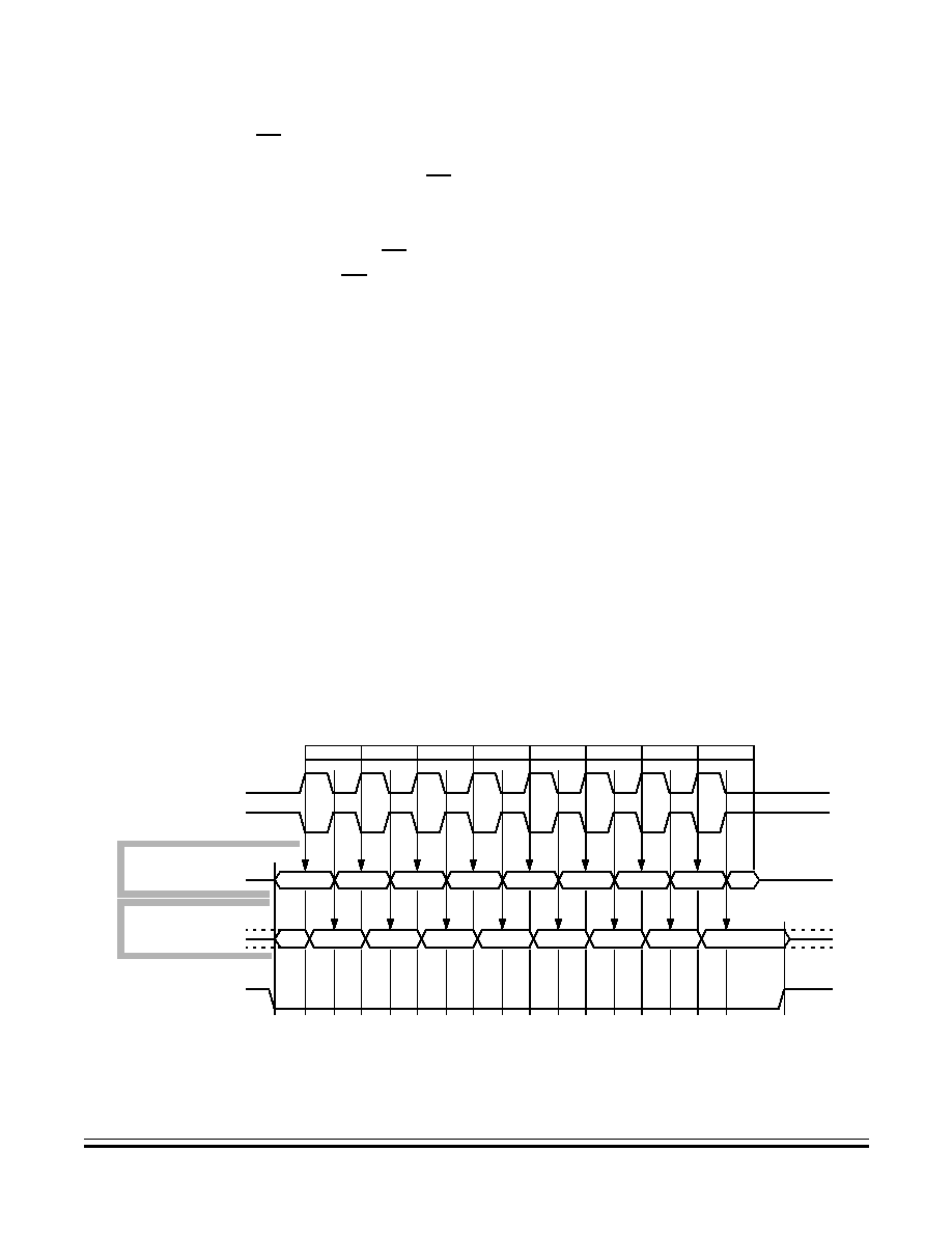
Serial Peripheral Interface (SPI)
SPI Signal Descriptions
M68HC11K Family
Technical Data
MOTOROLA
Serial Peripheral Interface (SPI)
171
8.4.4 Slave Select (SS)
The slave select (SS) input is used to target specific devices in the SPI
system. It must be pulled low on a targeted slave device prior to any
communication with a master and must remain low for the duration of the
transaction. SS must always be high on any device in master mode.
Pulling SS low on a master mode device generates a mode fault error
(see
8.5.1 Mode Fault Error
).
8.4.5 SPI Timing
Four possible timing relationships are available through control bits
CPOL (clock polarity) and CPHA (clock phase) in the SPCR. These bits
must be the same in both master and slave devices. The master device
always places data on the MOSI line approximately a half-cycle before
the SCK clock edge. This enables the slave device to latch the data. See
Figure 8-2
.
A write collision is normally a slave error because a slave has no control
over when a master initiates a transfer. A master knows when a transfer
is in progress, so there is no reason for a master to generate a
write-collision error, although the SPI logic can detect write collisions in
both master and slave devices.
Figure 8-2. Data Clock Timing Diagram
SCK CYCLE #
FOR REFERENCE
1
2
3
4
5
6
7
8
SCK (CPOL = 0)
SCK (CPOL = 1)
(CPHA = 0) DATA OUT
(CPHA = 1) DATA OUT
SS (TO SLAVE)
SAMPLE INPUT
SAMPLE INPUT
MSB
6
5
4
3
2
1
LSB
MSB
6
5
4
3
2
1
LSB

Technical Data
M68HC11K Family
172
Serial Peripheral Interface (SPI)
MOTOROLA
Serial Peripheral Interface (SPI)
CPOL selects an active high or low clock edge. CPHA selects one of two
transfer formats. When CPHA is cleared, the shift clock is ORed with SS.
Each slave's SS pin must be pulled high before it writes the next output
byte to its data register. If a slave writes to its data register while SS is
low, a write collision error occurs. When CPHA is set, SS may be left low
for several SPI characters. When there is only one SPI slave MCU, its
SS line may be tied to V
SS
if CPHA = 1 at all times.
The SPI configuration determines the characteristics of a transfer in
progress. For a master, a transfer begins when data is written to SPDR
and ends when SPIF is set. For a slave with CPHA cleared, a transfer
starts when SS goes low and ends when SS returns high. In this case,
SPIF is set at the middle of the eighth SCK cycle when data is
transferred from the shifter to the parallel data register, but the transfer
is still in progress until SS goes high. For a slave with CPHA set, transfer
begins when the SCK line goes to its active level, which is the edge at
the beginning of the first SCK cycle. The transfer ends when SPIF is set.
SCK in a slave must be inactive for at least two E-clock cycles between
byte transfers.
8.5 SPI System Errors
Two types of errors can be detected by the SPI system:
�
A mode fault error can occur when multiple devices attempt to act
in master mode simultaneously.
�
A write collision error results from an attempt to write data to the
SPDR while a transmission is in progress.
8.5.1 Mode Fault Error
A mode fault error occurs when the SS input line of an SPI system
configured as a master goes to active low, usually because two devices
have attempted to act as master at the same time. The resulting
contention between push-pull CMOS pin drivers can cause them
permanent damage. The mode fault disables the drivers in an attempt to
protect them. The MSTR control bit in the SPCR and all four DDRD

Serial Peripheral Interface (SPI)
SPI Registers
M68HC11K Family
Technical Data
MOTOROLA
Serial Peripheral Interface (SPI)
173
control bits associated with the SPI are cleared, effectively forcing the
pins to be high-impedance inputs. The mode fault error flag (MODF) is
set in the serial peripheral status register (SPSR). An interrupt is
generated, subject to masking by the SPIE control bit and the I bit in the
CCR. To disable the mode fault circuit, write a 1 to DDRD bit 5. This
configures port D bit 5 as a general-purpose output rather than SS.
Other precautions may be necessary to prevent driver damage. For
instance, if two devices are made masters at the same time, mode fault
does not help protect either one unless one of them selects the other as
slave. The amount of damage possible depends on the length of time
both devices attempt to act as master.
8.5.2 Write Collision Error
A write collision error occurs when the SPDR is written while a
transmission is in progress. The SPDR is not double buffered in the
transmit direction, so writes to the SPDR go directly into the SPI shift
register, which would corrupt any transfer in progress. The MCU protects
against this by preventing the write and generating the write collision
error. The transmission continues undisturbed.
A write collision is normally a slave error because a slave has no control
over when a master initiates a transfer. A master knows when a transfer
is in progress, so there is no reason for a master to generate a
write-collision error, although the SPI logic can detect write collisions in
both master and slave devices.
8.6 SPI Registers
The three SPI registers provide control, status, and data storage
functions respectively:
�
Serial peripheral control register (SPCR)
�
Serial peripheral status register (SPSR)
�
Serial peripheral data register (SPDR)

Technical Data
M68HC11K Family
174
Serial Peripheral Interface (SPI)
MOTOROLA
Serial Peripheral Interface (SPI)
NOTE:
Throughout this manual, the registers are discussed by function. In the
event that not all bits in a register are referenced, the bits that are not
discussed are shaded.
8.6.1 Serial Peripheral Control Register
SPIE -- Serial Peripheral Interrupt Enable Bit
0 = SPI interrupt disabled
1 = SPI interrupt is enabled each time the SPIF or MODF status
flag in SPSR is set.
SPE -- Serial Peripheral System Enable Bit
0 = SPI off
1 = SPI on -- PD[5:2] function as SPI signals
DWOM -- Port D Wired-OR Mode Bit
DWOM affects only the four SPI pins on port D, PD[5:2]. See also
7.9.2 Serial Communications Control Register 1
for a discussion
of the WOMS (wired-OR Mode for SCI pins) bit in the serial
communications control register 1 (SCCR1).
0 = Normal CMOS outputs
1 = Open-drain outputs
MSTR -- Master Mode Select Bit
0 = Slave mode
1 = Master mode
Address: $0028
Bit 7
6
5
4
3
2
1
Bit 0
Read:
SPIE
SPE
DWOM
MSTR
CPOL
CPHA
SPR1
SPR2
Write:
Reset:
0
0
0
0
0
1
U
U
U = Undefined
Figure 8-3. Serial Peripheral Control Register (SPCR)
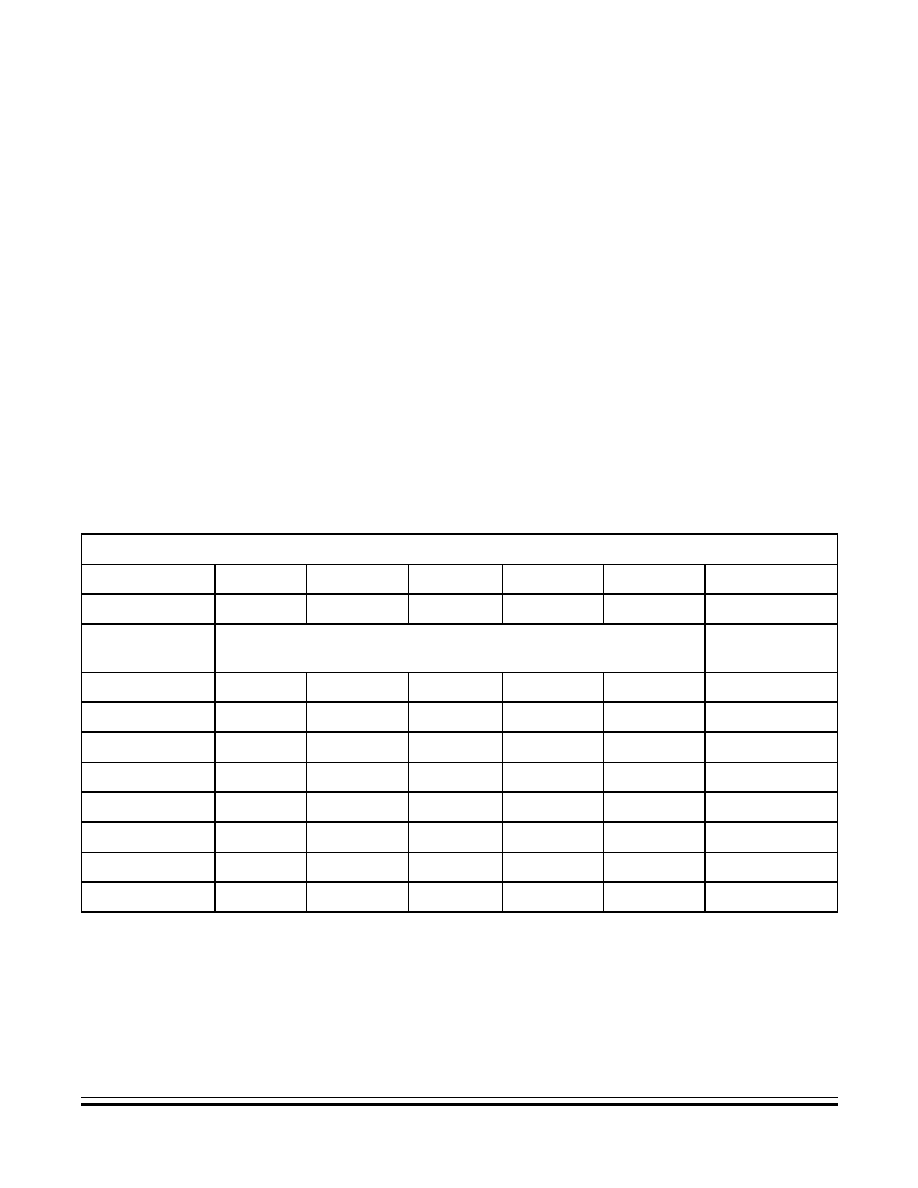
Serial Peripheral Interface (SPI)
SPI Registers
M68HC11K Family
Technical Data
MOTOROLA
Serial Peripheral Interface (SPI)
175
CPOL -- Clock Polarity Bit
When the clock polarity bit is cleared and data is not being
transferred, the SCK pin of the master device has a steady state low
value. When CPOL is set, SCK idles high.
CPHA -- Clock Phase Bit
The clock phase bit, in conjunction with the CPOL bit, controls the
clock-data relationship between master and slave. The CPHA bit
selects one of two different clocking protocols.
SPR[1:0] -- SPI Clock Rate Select Bits
On a master device, these two bits in conjunction with SPR2 in the
OPT2 register select the baud rate to be used as SCK. See
Table 8-1
.
These bits have no effect in slave mode.
Table 8-1. SPI+ Baud Rates
EXTAL Frequencies
EXTAL Freq.
8.0 MHz
12.0 MHz
16.0 MHz
20.0 MHz
24.0 MHz
Other EXTAL
E Clock Freq.
2.0 MHz
3.0 MHz
4.0 MHz
5.0 MHz
6.0 MHz
EXTAL
�
4
Control Bits
SPR[2:0]
SPI Baud Rate
E Clock
Divide by
0 0 0
1.0 MHz
1.5 MHz
2.0 MHz
2.5 MHz
3.0 MHz
2
0 0 1
500 kHz
750 kHz
1.0 MHz
1.3 kHz
1.5 MHz
4
0 1 0
125 kHz
187.5 kHz
250 kHz
312.5 kHz
375.0 kHz
16
0 1 1
62.5 kHz
93.8 kHz
125 kHz
156.3 kHz
187.5 kHz
32
1 0 0
250 kHz
375 kHz
500 kHz
625 kHz
750.0 kHz
8
1 0 1
125 kHz
187.5 kHz
250 kHz
312.5 kHz
375.0 kHz
16
1 1 0
31.3 kHz
46.9 kHz
62.5 kHz
78.1 kHz
93.8 kHz
64
1 1 1
15.6 kHz
23.4 kHz
31.3 kHz
39.1 kHz
46.9 kHz
128
Technical Data
M68HC11K Family
176
Serial Peripheral Interface (SPI)
MOTOROLA
Serial Peripheral Interface (SPI)
8.6.2 Serial Peripheral Status Register
SPIF -- SPI Transfer Complete Flag
SPIF is set upon completion of data transfer between the processor
and the external device. If SPIF goes high, and if SPIE is set, a serial
peripheral interrupt is generated. To clear the SPIF bit, read the SPSR
with SPIF set, then access the SPDR. Unless SPSR is read (with
SPIF set) first, attempts to write SPDR are inhibited.
WCOL -- Write Collision Bit
Clearing the WCOL bit is accomplished by reading the SPSR (with
WCOL set) followed by an access of SPDR.
0 = No write collision
1 = Write collision
MODF -- Mode Fault Bit
To clear the MODF bit, read the SPSR (with MODF set), then write to
the SPCR.
0 = No mode fault
1 = Mode fault
Address: $0029
Bit 7
6
5
4
3
2
1
Bit 0
Read:
SPIF
WCOL
0
MODF
0
0
0
0
Write:
Reset:
0
0
0
0
0
0
0
0
Figure 8-4. Serial Peripheral Status Register (SPSR)

Serial Peripheral Interface (SPI)
SPI Registers
M68HC11K Family
Technical Data
MOTOROLA
Serial Peripheral Interface (SPI)
177
8.6.3 Serial Peripheral Data Register
The SPDR is used when transmitting or receiving data on the serial bus.
Only a write to this register initiates transmission or reception of a byte,
and this only occurs in the master device. At the completion of
transferring a byte of data, the SPIF status bit is set in both the master
and slave devices.
A read of the SPDR is actually a read of a buffer. To prevent an overrun
and the loss of the byte that caused the overrun, the first SPIF must be
cleared by the time a second transfer of data from the shift register to the
read buffer is initiated.
A write to SPDR goes directly to the transmission shift register.
A read of the SPDR retrieves data from the read data buffer.
Address: $002A
Bit 7
6
5
4
3
2
1
Bit 0
Read:
Bit 7
Bit 6
Bit 5
Bit 4
Bit 3
Bit 2
Bit 1
Bit 0
Write:
Reset:
0
0
0
0
0
0
0
0
Figure 8-5. Serial Peripheral Data Register (SPDR)
Technical Data
M68HC11K Family
178
Serial Peripheral Interface (SPI)
MOTOROLA
Serial Peripheral Interface (SPI)
8.6.4 Port D Data Direction Register
DDD5 Bit
Bit 5 of the port D data register (PD5) is dedicated as the slave select
(SS) input. In SPI slave mode, DDD5 has no meaning or effect. In SPI
master mode, DDD5 affects PD5 as follows:
0 = PD5 is an error-detect input to the SPI.
1 = PD5 is configured as a general-purpose output line.
DDD[4:2] Bits
When the SPI is enabled, SPI input pins remain functioning
regardless of the state of the corresponding DDD[4:2] bits. For SPI
output pins, however, the corresponding DDD[4:2] bits must be set or
the pins will function as general-purpose inputs.
Address: $0009
Bit 7
6
5
4
3
2
1
Bit 0
Read:
0
0
DDD5
DDD4
DDD3
DDD2
DDD1
DDD0
Write:
Reset:
0
0
0
0
0
0
0
0
Figure 8-6. Port D Data Direction Register (DDRD)
Serial Peripheral Interface (SPI)
SPI Registers
M68HC11K Family
Technical Data
MOTOROLA
Serial Peripheral Interface (SPI)
179
8.6.5 System Configuration Options 2
LSBF -- Least Significant Bit First Enable Bit
Setting LSBF causes data to be transmitted LSB first (the default is
MSB first). LSBF does not affect bit positions in the data register;
reads and writes always have MSB in bit 7.
SPR2 -- SPI Clock Rate Select Bit
SPR2 adds a divide-by-4 prescaler to the SPI clock chain. With the
two bits in the SPCR, this specifies the SPI clock rate. See
Table 8-1
.
Address: $0038
Bit 7
6
5
4
3
2
1
Bit 0
Read:
LIRDV
CWOM
STRCH
(1)
IRVNE
LSBF
SPR2
XDV1
XDV0
Write:
Reset:
0
0
0
--
0
0
0
0
1. Not available on M68HC11K devices
Figure 8-7. System Configuration Options 2 Register (OPT2)

Technical Data
M68HC11K Family
180
Serial Peripheral Interface (SPI)
MOTOROLA
Serial Peripheral Interface (SPI)

M68HC11K Family
Technical Data
MOTOROLA
Timing System
181
Technical Data -- M68HC11K Family
Section 9. Timing System
9.1 Contents
9.2
Introduction . . . . . . . . . . . . . . . . . . . . . . . . . . . . . . . . . . . . . . . 182
9.3
Timer Structure . . . . . . . . . . . . . . . . . . . . . . . . . . . . . . . . . . . . 183
9.4
Input Capture and Output Compare Overview . . . . . . . . . . . . 185
9.4.1
Timer Counter Register . . . . . . . . . . . . . . . . . . . . . . . . . . . 188
9.4.2
Timer Interrupt Flag 2 Register . . . . . . . . . . . . . . . . . . . . . 189
9.4.3
Timer Interrupt Mask 2 Register. . . . . . . . . . . . . . . . . . . . . 189
9.4.4
Port A Data Direction Register . . . . . . . . . . . . . . . . . . . . . . 190
9.4.5
Pulse Accumulator Control Register . . . . . . . . . . . . . . . . . 191
9.5
Input Capture (IC) . . . . . . . . . . . . . . . . . . . . . . . . . . . . . . . . . . 191
9.5.1
Timer Input Capture Registers . . . . . . . . . . . . . . . . . . . . . . 192
9.5.2
Timer Input Capture 4/Output Compare 5 Register . . . . . . 193
9.5.3
Timer Interrupt Flag 1 Register . . . . . . . . . . . . . . . . . . . . . 194
9.5.4
Timer Interrupt Mask 1 Register. . . . . . . . . . . . . . . . . . . . . 194
9.5.5
Timer Control 2 Register . . . . . . . . . . . . . . . . . . . . . . . . . . 195
9.6
Output Compare (OC) . . . . . . . . . . . . . . . . . . . . . . . . . . . . . . 196
9.6.1
Timer Output Compare Registers . . . . . . . . . . . . . . . . . . . 197
9.6.2
Timer Input Capture 4/Output Compare 5 Register . . . . . . 199
9.6.3
Timer Interrupt Flag 1 Register . . . . . . . . . . . . . . . . . . . . . 199
9.6.4
Timer Interrupt Mask 1 Register. . . . . . . . . . . . . . . . . . . . . 200
9.6.5
Timer Control 1 Register . . . . . . . . . . . . . . . . . . . . . . . . . . 200
9.6.6
Timer Compare Force Register . . . . . . . . . . . . . . . . . . . . . 201
9.6.7
Output Compare 1 Mask Register . . . . . . . . . . . . . . . . . . . 202
9.6.8
Output Compare 1 Data Register. . . . . . . . . . . . . . . . . . . . 202
9.7
Pulse Accumulator (PA) . . . . . . . . . . . . . . . . . . . . . . . . . . . . . 203
9.7.1
Port A Data Direction Register . . . . . . . . . . . . . . . . . . . . . . 205
9.7.2
Pulse Accumulator Control Register . . . . . . . . . . . . . . . . . 205
9.7.3
Timer Interrupt Flag 2 Register . . . . . . . . . . . . . . . . . . . . . 206

Technical Data
M68HC11K Family
182
Timing System
MOTOROLA
Timing System
9.7.4
Timer Interrupt Mask 2 Register. . . . . . . . . . . . . . . . . . . . . 207
9.7.5
Pulse Accumulator Count Register . . . . . . . . . . . . . . . . . .208
9.8
Real-Time Interrupt (RTI) . . . . . . . . . . . . . . . . . . . . . . . . . . . . 208
9.8.1
Timer Interrupt Flag 2 Register . . . . . . . . . . . . . . . . . . . . . 209
9.8.2
Timer Interrupt Mask 2 Register. . . . . . . . . . . . . . . . . . . . . 209
9.8.3
Pulse Accumulator Control Register . . . . . . . . . . . . . . . . . 210
9.9
Pulse-Width Modulator (PWM) . . . . . . . . . . . . . . . . . . . . . . . . 211
9.9.1
PWM System Description. . . . . . . . . . . . . . . . . . . . . . . . . . 211
9.9.2
Pulse-Width Modulation Control Registers. . . . . . . . . . . . . 213
9.9.2.1
Pulse-Width Modulation Timer
Clock Select Register . . . . . . . . . . . . . . . . . . . . . . . . 213
9.9.2.2
Pulse-Width Modulation Timer Polarity Register . . . . . . 215
9.9.2.3
Pulse-Width Modulation Timer Prescaler Register . . . .215
9.9.2.4
Pulse-Width Modulation Timer Enable Register . . . . . . 216
9.9.2.5
Pulse-Width Modulation Timer
Counters1 to 4 Registers . . . . . . . . . . . . . . . . . . . . . 217
9.9.2.6
Pulse-Width Modulation Timer
Periods 1 to 4 Registers . . . . . . . . . . . . . . . . . . . . . . 218
9.9.2.7
Pulse-Width Modulation Timer
Duty Cycle 1 to 4 Registers . . . . . . . . . . . . . . . . . . .219
9.2 Introduction
M68HC11 microcontrollers contain an extensive timing system to
support a wide variety of timer-related functions. This section discusses
the nature of the timing system and presents details of timer-related
functions including:
�
Input capture/output compare (IC/OC)
�
Real-time interrupt (RTI)
�
Pulse accumulator (PA)
�
Pulse width modulation (PWM)
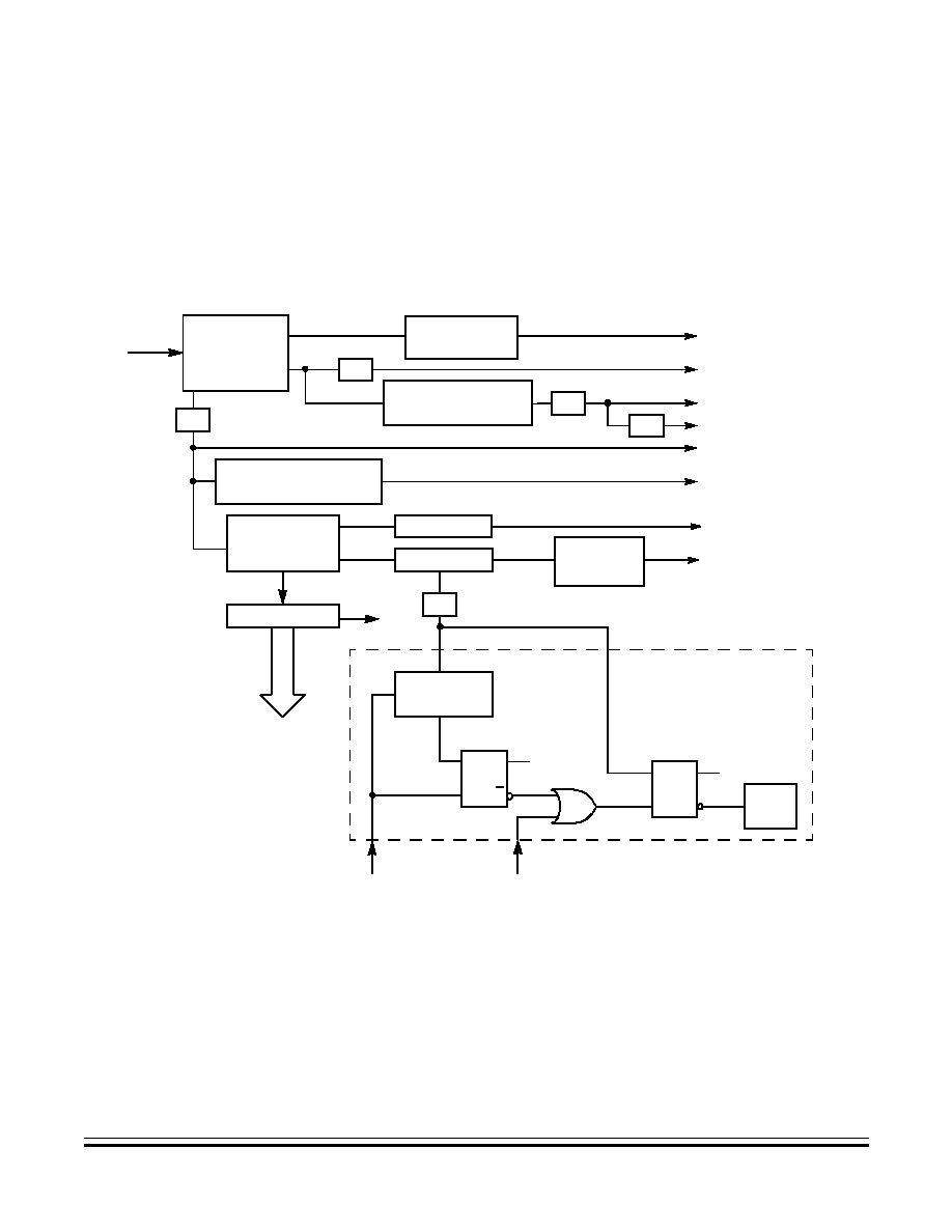
Timing System
Timer Structure
M68HC11K Family
Technical Data
MOTOROLA
Timing System
183
9.3 Timer Structure
As
Figure 9-1
shows, the primary system clocks, including the E clock
and the internal PH2 bus clock, are derived from the oscillator output
divided by four.
Figure 9-1. Timer Clock Divider Chains
(
�
1, 2, 3, 4, 5......8191)
SBR[12:0]
SCI RECEIVER CLOCK
SCI TRANSMIT CLOCK
XOUT
E CLOCK
PH 2 (INTERNAL BUS
PRESCALER
(
�
2, 4, 8, 16, 32, 64, 128)
SPR[2:0]
�
2
�
16
�
4
SPI
�
1, 4, 6, 8
XDV[1:0].
TCNT
IC/OC
PRESCALER
(
�
1, 4, 8, 16)
PR[1:0]
POSTSCALER
PULSE ACCUMULATOR
E
�
2
6
REAL-TIME INTERRUPT
E
�
2
13
�
4
PRESCALER
(� 1, 2, 4, 8)
RTR[1:0]
PRESCALER
(
�
1, 4, 16, 64)
CR[1:0]
S
Q
R
Q
S
Q
R
Q
FORCE
COP
RESET
SYSTEM
RESET
CLEAR COP
TIMER
TOF
POSTSCALER
OSCILLATOR
E
�
2
15
CLOCK)
�
4
EXTAL

Technical Data
M68HC11K Family
184
Timing System
MOTOROLA
Timing System
The PH2 bus clock feeds four primary divider chains. The functions
supplied by each of these chains are:
1. Serial peripheral interface (SPI)
2. Input capture/output compare (IC/OC)
3. Pulse accumulator (PA)
4. RTI and COP watchdog circuit
The SPI prescale factor is determined by bits SPR[2] in the system
configuration options 2 (OPT2) register and SPR[1:0] in the serial
peripheral control register (SPCR). See
8.6.1 Serial Peripheral Control
Register
and
8.6.5 System Configuration Options 2
.
The input capture and output compare functions are based on a 16-bit
free-running counter, which is driven by the PH2 clock divided by a
programmable prescaler. Bits PR[1:0] of the timer interrupt mask 2
(TMSK2) register enable the user to select one of four divisors: 1, 4, 8,
or 16. The output of this prescaler, referred to as the main timer, feeds
the divider chains for the pulse accumulator, RTI, and COP circuits as
well as the free-running counter.
Table 9-1
shows main timer
frequencies and periods available from the most common crystal inputs.
Table 9-1. Main Timer Rates
EXTAL Frequencies
EXTAL Freq.
8.0 MHz
12.0 MHz
16.0 MHz
20.0 MHz
20.0 MHz
Other EXTAL
E Clock Freq.
2.0 MHz
3.0 MHz
4.0 MHz
5.0 MHz
5.0 MHz
EXTAL/4
E Clock Period
500 ns
333 ns
250 ns
200 ns
200 ns
1/E
Control Bits
PR[1:0]
Main Timer Period
(1 Count/Timer Overflow)
1 Count
Timer Overflow
0 0
500 ns
32.768 ms
333 ns
21.845 ms
250 ns
16.384 ms
200 ns
13.107 ms
167 ns
10.923 ms
1
�
E
2
16
�
E
0 1
2.0
�
s
131.07 ms
1.3
�
s
87.381 ms
1.0
�
s
85.536 ms
800 ns
52.429 ms
667 ns
43.961 ms
4
�
E
2
18
�
E
1 0
4.0
�
s
262.14 ms
2.667
�
s
174.76 ms
2.0
�
s
131.07 ms
1.6
�
s
104.86 ms
1.333
�
s
87.381 ms
8
�
E
2
19
�
E
1 1
8.0
�
s
524.29 ms
5.333
�
s
349.53 ms
4.0
�
s
262.14 ms
3.2
�
s
209.72 ms
2.667
�
s
174.76 ms
16
�
E
2
20
�
E

Timing System
Input Capture and Output Compare Overview
M68HC11K Family
Technical Data
MOTOROLA
Timing System
185
The free-running counter begins incrementing from $0000 as the MCU
comes out of reset and continues to the maximum count, $FFFF. At the
maximum count, the counter rolls over to $0000, sets the timer overflow
flag (TOF) in the timer interrupt flag 2 (TFLG2) register, and continues to
increment. The value in this counter can be read in the timer counter
(TCNT) register, but cannot be written or changed except by reset.
The pulse accumulator, described in
9.7 Pulse Accumulator (PA)
,
derives its clock by post-scaling the main timer so that the output
frequency is always E clock divided by 64. This clock drives an 8-bit
counter while the pulse accumulator is operating in event counting
mode.
RTI is a programmable periodic interrupt circuit that can be used to pace
the execution of software routines, as described in
9.8 Real-Time
Interrupt (RTI)
. The clock driving this function is also derived from the
clock driving the free-running counter. The post-scaler output of this
chain runs at a frequency of E clock divided by 2
13
.
The COP watchdog timer (
5.3.3 Computer Operating Properly (COP)
System
) further divides the RTI clock by four to drive its circuitry at a
frequency of E clock divided by 2
15
.
9.4 Input Capture and Output Compare Overview
The M68HC11K series features:
�
Three input capture channels
�
Four output compare channels
�
One channel that can be selected to perform either input capture
or output compare
Each of the three input capture functions has its own 16-bit input capture
register (time capture latch) and each of the output compare functions
has its own 16-bit compare register. All timer functions, including the
timer overflow and RTI, have their own interrupt controls and separate
interrupt vectors.

Technical Data
M68HC11K Family
186
Timing System
MOTOROLA
Timing System
Figure 9-2
shows the capture/compare system block diagram. The port
A pin control block includes logic for timer functions and for
general-purpose I/O. This block contains the edge-detection logic for
pins PA[2:0] as well as the control logic that enables edge selection for
the input capture trigger.
�
PA[2:0] can serve either as input capture pins IC[1:3] or as
general-purpose input/output (GPIO).
�
PA[6:4] can serve either as drivers for output compare functions
OC[2:4] or GPIO.
�
PA3 can be used for GPIO, input capture 4, output compare 5, or
output compare 1.
�
Output compare 1 (OC1) has extra control logic which gives it
optional control of any combination of the PA[7:3] pins.
�
The PA7 pin can be used as a GPIO pin, as an input to the pulse
accumulator, or as an OC1 output pin.
Reading the port A register returns the actual pin level on any pin
functioning as an input, and the logic level of the internal pin driver (NOT
the pin level) on any pin functioning as an output. This is true whether
the pins are configured for timer functions or GPIO. Writing to port A pins
configured for timer functions has no visible effect; the writes are latched
but do not drive the pins.
Registers common to both the input capture and output compare
functions include:
�
Timer counter register (TCNT)
�
Timer interrupt flag 2 (TFLG2)
�
Timer interrupt mask 2 (TMSK2)
�
Data direction register A (DDRA)
�
Pulse accumulator control register (PACTL)
NOTE:
Throughout this manual, the registers are discussed by function. In the
event that not all bits in a register are referenced, the bits that are not
discussed are shaded.

Timing System
Input Capture and Output Compare Overview
M68HC11K Family
Technical Data
MOTOROLA
Timing System
187
Figure 9-2. Capture/Compare Block Diagram
SYSTEM
16-BIT LATCH
CLK
4
5
6
7
8
PORT A
PIN CONTROL
OC1I
OC2I
OC3I
OC4I
I4/O5I
TFLG 1
STATUS
FLAGS
FOC1
FOC2
FOC3
FOC4
FOC5
OC1F
OC2F
OC3F
OC4F
I4/O5F
PA3
PA4
PA5
PA6
PA7
I4/O5
16-BIT COMPARATOR =
TOC1 (HI)
TOC1 (LO)
16-BIT COMPARATOR =
TOC2 (HI)
TOC2 (LO)
16-BIT COMPARATOR =
TOC3 (HI)
TOC3 (LO)
16-BIT COMPARATOR =
TOC4 (HI)
TOC4 (LO)
16-BIT COMPARATOR =
TI4/O5 (HI)
TI4/O5 (LO)
16-BIT FREE
COUNTER
TCNT (HI)
TCNT (LO)
9
TOI
TOF
INTERRUPT REQUESTS
PRESCALER -- DIVIDE BY
1, 4, 8, 16
PR1
16-BIT TIMER BUS
OC5
IC4
TMSK 1
INTERRUPT
ENABLES
CFORC
FORCE OUTPUT
PIN
FUNCTIONS
PA0
3
2
1
IC1I
IC2I
IC3I
IC1F
IC2F
IC3F
PA1
PA2
16-BIT LATCH
TIC1 (HI)
TIC1
(LO)
CLK
16-BIT LATCH
TIC2 (HI)
TIC2 (LO)
CLK
16-BIT LATCH
TIC3 (HI)
TIC3 (LO)
CLK
IC3
IC2
IC1
PR0
CLOCK
OC1
OC2/OC1
OC3/OC1
OC4/OC1
IC4/OC5
OC1
COMPARE
RUNNING
BIT 7
BIT 6
BIT 5
BIT 4
BIT 3
BIT 2
BIT 1
BIT 0

Technical Data
M68HC11K Family
188
Timing System
MOTOROLA
Timing System
9.4.1 Timer Counter Register
TCNT reflects the current value in the free-running counter. Input
capture functions use this number to mark the time of an external event,
and output compare functions use it to determine the time at which to
generate an event.
In normal modes, TCNT is a read-only register. Writes to TCNT in
normal modes have no effect. TCNT can be read and written in special
modes.
Bit 7
6
5
4
3
2
1
Bit 0
Address: $000E -- TCNT (High)
Read:
Bit 15
Bit 14
Bit 13
Bit 12
Bit 11
Bit 10
Bit 9
Bit 8
Write:
Reset:
0
0
0
0
0
0
0
0
Address: $000F -- TCNT (Low)
Read:
Bit 7
Bit 6
Bit 5
Bit 4
Bit 3
Bit 2
Bit 1
Bit 0
Write:
Reset:
0
0
0
0
0
0
0
0
= Unimplemented
Figure 9-3. Timer Counter Register (TCNT)
Timing System
Input Capture and Output Compare Overview
M68HC11K Family
Technical Data
MOTOROLA
Timing System
189
9.4.2 Timer Interrupt Flag 2 Register
Clear each flag by writing a 1 to the corresponding bit position.
TOF -- Timer Overflow Flag
Set when TCNT changes from $FFFF to $0000.
9.4.3 Timer Interrupt Mask 2 Register
Bits in TMSK2 correspond bit for bit with flag bits in TFLG2.
TOI -- Timer Overflow Interrupt Enable Bit
0 = Timer overflow interrupt disabled
1 = An interrupt request is generated when TOF is set.
Address: $0025
Bit 7
6
5
4
3
2
1
Bit 0
Read:
TOF
RTIF
PAOVF
PAIF
0
0
0
0
Write:
Reset:
0
0
0
0
0
0
0
0
Figure 9-4. Timer Interrupt Flag 2 (TFLG2)
Address: $0024
Bit 7
6
5
4
3
2
1
Bit 0
Read:
TOI
RTII
PAOVI
PAII
0
0
PR1
PR0
Write:
Reset:
0
0
0
0
0
0
0
0
Figure 9-5. Timer Interrupt Mask 2 (TMSK2)
Technical Data
M68HC11K Family
190
Timing System
MOTOROLA
Timing System
PR[1:0] -- Timer Prescaler Select Bits
These bits determine the main timer prescale divisor, as shown in
Table 9-2
. The system bus (E clock) frequency is divided by this
number to produce the clock which drives the free-running counter.
Refer to
Table 9-1
for specific timing values.
In normal modes, PR[1:0] can be written only once, and the write must
be within 64 cycles after reset.
9.4.4 Port A Data Direction Register
DDA3 -- Data Direction Control for Port A, Bit 3
0 = PA3 configured as an input
1 = PA3 configured as an output
Table 9-2. Timer Prescale
PR[1:0]
Prescaler
0 0
1
0 1
4
1 0
8
1 1
16
Address: $0001
Bit 7
6
5
4
3
2
1
Bit 0
Read:
DDA7
DDA6
DDA5
DDA4
DDA3
DDA2
DDA1
DDA0
Write:
Reset:
0
0
0
0
0
0
0
0
Figure 9-6. Port A Data Direction Register (DDRA)
Timing System
Input Capture (IC)
M68HC11K Family
Technical Data
MOTOROLA
Timing System
191
9.4.5 Pulse Accumulator Control Register
I4/O5 -- Input Capture 4/Output Compare 5 Bit
0 = Configure PA3 as OC5
1 = Configure PA3 as IC4
To configure PA3 as input compare 4, clear DDA3 and set I4/05. To
configure PA3 as output compare 5, set DDA3 and clear I4/05. If the
DDA3 bit is set (configuring PA3 as an output) and IC4 is enabled,
writing a one to TI4/O5 causes an input capture. Writing to TI4/O5 has
no effect when DDA3 is cleared and/or OC5 is enabled.
9.5 Input Capture (IC)
The input capture function records the time an external event occurs by
latching the value of the free-running counter into one of the timer input
capture (TIC) registers when a selected edge is detected at its
associated timer input pin. Software can store latched values and use
them to compute the period and duration of events. For example, by
storing the times of successive edges of an incoming signal, software
can determine the period and pulse width of a signal. To measure the
period, two successive edges of the same polarity are captured. To
measure pulse width, two alternate polarity edges are captured.
Capture requests are latched on the opposite half cycle of PH2 from
when the timer counter is being incremented. This synchronization
process introduces a delay between edge occurrence and counter value
detection. Because these delays offset each other when the time
between two edges is measured, they can be ignored. There is a similar
delay for output compare between the actual compare point and when
the output pin changes state.
Address: $0026
Bit 7
6
5
4
3
2
1
Bit 0
Read:
0
PAEN
PAMOD
PEDGE
0
I4/O5
RTR1
RTR0
Write:
Reset:
0
0
0
0
0
0
0
0
Figure 9-7. Pulse Accumulator Control Register (PACTL)

Technical Data
M68HC11K Family
192
Timing System
MOTOROLA
Timing System
9.5.1 Timer Input Capture Registers
Bit 7
6
5
4
3
2
1
Bit 0
Address: $0010 -- TIC1 (High)
Read:
Bit 15
Bit 14
Bit 13
Bit 12
Bit 11
Bit 10
Bit 9
Bit 8
Write:
Reset:
Unaffected by reset
Address: $0011 -- TIC1 (Low)
Read:
Bit 7
Bit 6
Bit 5
Bit 4
Bit 3
Bit 2
Bit 1
Bit 0
Write:
Reset:
Unaffected by reset
Address: $0012 -- TIC2 (High)
Read:
Bit 15
Bit 14
Bit 13
Bit 12
Bit 11
Bit 10
Bit 9
Bit 8
Write:
Reset:
Unaffected by reset
Address: $0013 -- TIC2 (Low)
Read:
Bit 7
Bit 6
Bit 5
Bit 4
Bit 3
Bit 2
Bit 1
Bit 0
Write:
Reset:
Unaffected by reset
Address: $0014-- TIC3 (High)
Read:
Bit 15
Bit 14
Bit 13
Bit 12
Bit 11
Bit 10
Bit 9
Bit 8
Write:
Reset:
Unaffected by reset
Address: $0015 -- TIC3 (Low)
Read:
Bit 7
Bit 6
Bit 5
Bit 4
Bit 3
Bit 2
Bit 1
Bit 0
Write:
Reset:
Unaffected by reset
Figure 9-8. Timer Input Capture Registers (TIC1�TIC3)
Timing System
Input Capture (IC)
M68HC11K Family
Technical Data
MOTOROLA
Timing System
193
9.5.2 Timer Input Capture 4/Output Compare 5 Register
TI4/05 functions as the input capture register for IC4 when PA3 is
configured for input capture 4.
When an edge on an input capture pin has been detected and
synchronized, the 16-bit free-running counter value is latched in the
associated input capture register pair in a single 16-bit parallel transfer.
The latch occurs on the opposite half-cycle of the phase two clock from
when the timer counter is incremented. This ensures a stable count
value whenever a capture occurs.
Input capture values can be retrieved from a TIC register with two
successive 8-bit reads. Reading the high-order byte inhibits a new
capture transfer for one bus cycle to ensure that the successive
low-order byte read corresponds with it. If a new input capture occurs
immediately after a high-order byte read, transfer is delayed for an
additional cycle, but the new value is not lost. To assure coherency
between the two bytes, use a double-byte read instruction such as LDD.
Bit 7
6
5
4
3
2
1
Bit 0
Address: $001E -- TI4/O5 (High)
Read:
Bit 15
Bit 14
Bit 13
Bit 12
Bit 11
Bit 10
Bit 9
Bit 8
Write:
Reset:
1
1
1
1
1
1
1
1
Address: $001F -- TI4/O5 (Low)
Read:
Bit 7
Bit 6
Bit 5
Bit 4
Bit 3
Bit 2
Bit 1
Bit 0
Write:
Reset:
1
1
1
1
1
1
1
1
Figure 9-9. Timer Input Capture 4/Output
Compare 5 Register (TI4/O5)
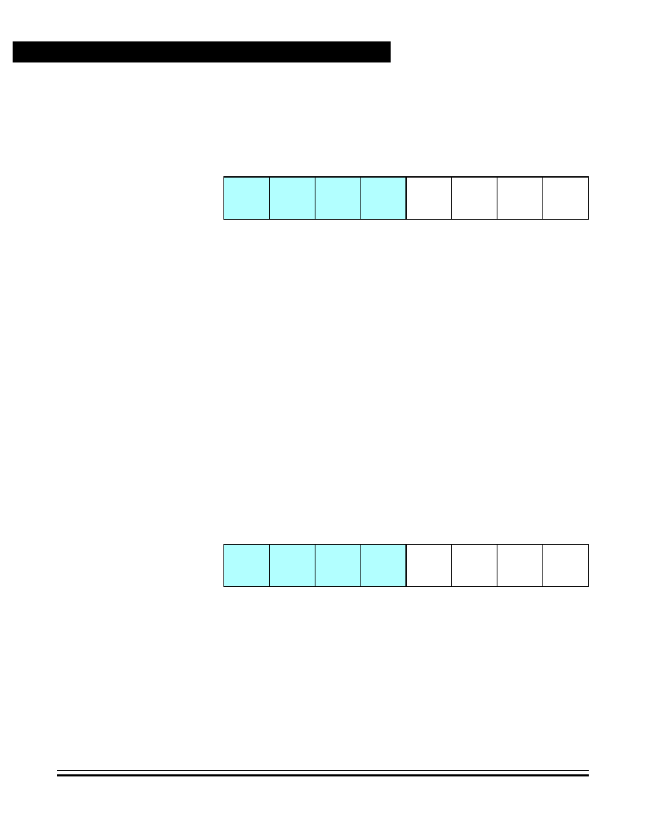
Technical Data
M68HC11K Family
194
Timing System
MOTOROLA
Timing System
9.5.3 Timer Interrupt Flag 1 Register
Clear each flag by writing a 1 to the corresponding bit position.
ICxF -- Input Capture x Flag
Set each time a selected active edge is detected on the
corresponding input capture line.
I4/O5F -- Input Capture 4/Output Compare 5 Flag
Set each time a selected active edge is detected on the IC4 line if IC4
is enabled.
9.5.4 Timer Interrupt Mask 1 Register
Bits in TMSK1 correspond bit for bit with flag bits in TFLG1.
ICxI -- Input Capture Interrupt Enable Bit
If the ICxI enable bit is set when the ICxF flag bit is set, a hardware
interrupt sequence is requested.
Address: $0023
Bit 7
6
5
4
3
2
1
Bit 0
Read:
OC1F
OC2F
OC3F
OC4F
I4/O5F
IC1F
IC2F
IC3F
Write:
Reset:
0
0
0
0
0
0
0
0
Figure 9-10. Timer Interrupt Flag 1 Register (TFLG1)
Address: $0022
Bit 7
6
5
4
3
2
1
Bit 0
Read:
OC1I
OC2I
OC3I
OC4I
I4/O5I
IC1I
IC2I
IC3I
Write:
Reset:
0
0
0
0
0
0
0
0
Figure 9-11. Timer Interrupt Mask 1 Register (TMSK1)
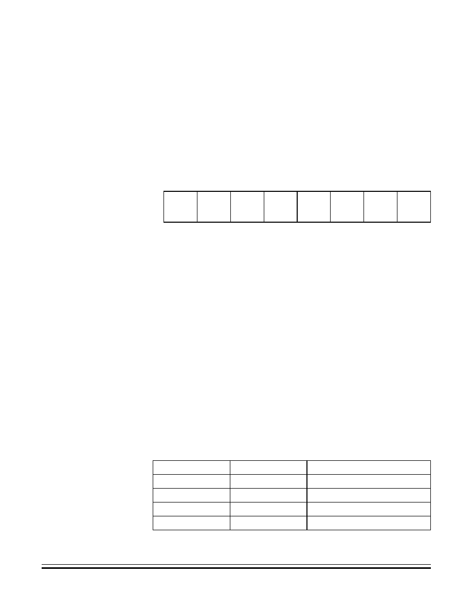
Timing System
Input Capture (IC)
M68HC11K Family
Technical Data
MOTOROLA
Timing System
195
I4/O5I -- Input Capture 4 or Output Compare 5 Interrupt Enable Bit
If I4/O5I is set when IC4 is enabled and the I4/O5F flag bit is set, a
hardware interrupt sequence is requested.
9.5.5 Timer Control 2 Register
EDGx[B:A] -- Input Capture Edge Control Bits
These bit pairs determine the edge polarities on the input capture pins
that trigger the corresponding input capture functions. Each of the
input capture functions can be independently configured to detect
rising edges only, falling edges only, any edge (rising or falling), or to
disable the input capture function. The input capture functions
operate independently of each other and can capture the same TCNT
value if the input edges are detected within the same timer count
cycle.
Each EDGx bit pair is cleared (IC function disabled) by reset and must
be encoded according to the values in
Table 9-3
to configure the
corresponding input capture edge detector circuit. IC4 functions only
if the I4/O5 bit in the PACTL register is set.
Address: $0021
Bit 7
6
5
4
3
2
1
Bit 0
Read:
EDG4B
EDG4A
EDG1B
EDG1A
EDG2B
EDG2A
EDG3B
EDG3A
Write:
Reset:
0
0
0
0
0
0
0
0
Figure 9-12. Timer Control 2 Register (TCTL2)
Table 9-3. Input Capture Edge Selection
EDGxB
EDGxA
ICx Configuration
0
0
Capture disabled
0
1
Capture on rising edges only
1
0
Capture on falling edges only
1
1
Capture on any edge

Technical Data
M68HC11K Family
196
Timing System
MOTOROLA
Timing System
9.6 Output Compare (OC)
The output compare (OC) function generates a programmed action
when the 16-bit counter reaches a specified value. Each of the five
output compare functions contains a separate 16-bit timer output
compare (TOC) register and a dedicated 16-bit comparator. Each TOC
register is set to $FFFF on reset. When an OC channel is enabled, the
value in its TOC register is compared to the free-running counter value
during each E-clock cycle. When the values match, the channel's output
compare flag is set in timer interrupt flag 1 (TFLG1). If the channel's
interrupt is enabled in the timer interrupt mask register 1 (TMSK1), an
interrupt is generated. Also, the corresponding timer output pin is
toggled or driven to a specified logic level. This pin activity occurs on
each successful compare, whether or not the OCxF flag in the TFLG1
register was previously cleared.
The pin action for each of the OC channels [5:2] is controlled by a pair of
bits (OMx and OLx) in the TCTL1 register and affects only the channel's
associated pin. A successful OC1 compare can affect any or all five of
the OC pins. The action taken when a match is found for OC1 is
controlled by two 8-bit registers:
�
Output compare 1 mask register (OC1M)
�
Output compare 1 data register (OC1D)
OC1M specifies which port A outputs are to be used, and OC1D
specifies the data placed on these port pins.
Although the M68HC11K series devices have four built-in pulse-width
modulation (PWM) channels (
9.9 Pulse-Width Modulator (PWM)
), the
output compare function can be used to produce an additional
pulse-width modulated waveform. To produce a pulse of a specific
duration:
�
Write a value to the output compare register that represents the
time the leading edge of the pulse is to occur.
�
Use OC1D to select either a high or low output, depending on the
polarity of the pulse being produced.
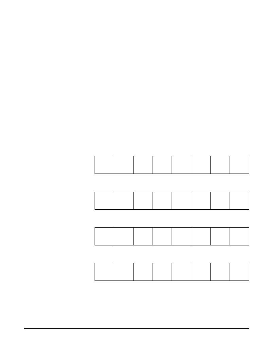
Timing System
Output Compare (OC)
M68HC11K Family
Technical Data
MOTOROLA
Timing System
197
�
After a match occurs, change the appropriate OC1D bit to the
opposite polarity, then add a value representing the width of the
pulse to the original value and write it to the output compare
register.
Because the pin state changes occur at specific values of the
free-running counter, the pulse width can be controlled accurately to the
resolution of the free-running counter, independent of software
latencies. To generate an output signal of a specific frequency and duty
cycle, repeat this pulse-generating procedure.
9.6.1 Timer Output Compare Registers
Bit 7
6
5
4
3
2
1
Bit 0
Address: $0016 -- TOC1 (High)
Read:
Bit 15
Bit 14
Bit 13
Bit 12
Bit 11
Bit 10
Bit 9
Bit 8
Write:
Reset:
1
1
1
1
1
1
1
1
Address: $0017 -- TOC1 (Low)
Read:
Bit 7
Bit 6
Bit 5
Bit 4
Bit 3
Bit 2
Bit 1
Bit 0
Write:
Reset:
1
1
1
1
1
1
1
1
Address: $0018 -- TOC2 (High)
Read:
Bit 15
Bit 14
Bit 13
Bit 12
Bit 11
Bit 10
Bit 9
Bit 8
Write:
Reset:
1
1
1
1
1
1
1
1
Address: $0019 -- TOC2 (Low)
Read:
Bit 7
Bit 6
Bit 5
Bit 4
Bit 3
Bit 2
Bit 1
Bit 0
Write:
Reset:
1
1
1
1
1
1
1
1
Figure 9-13. Timer Output Compare
Registers (TOC1�TOC4)
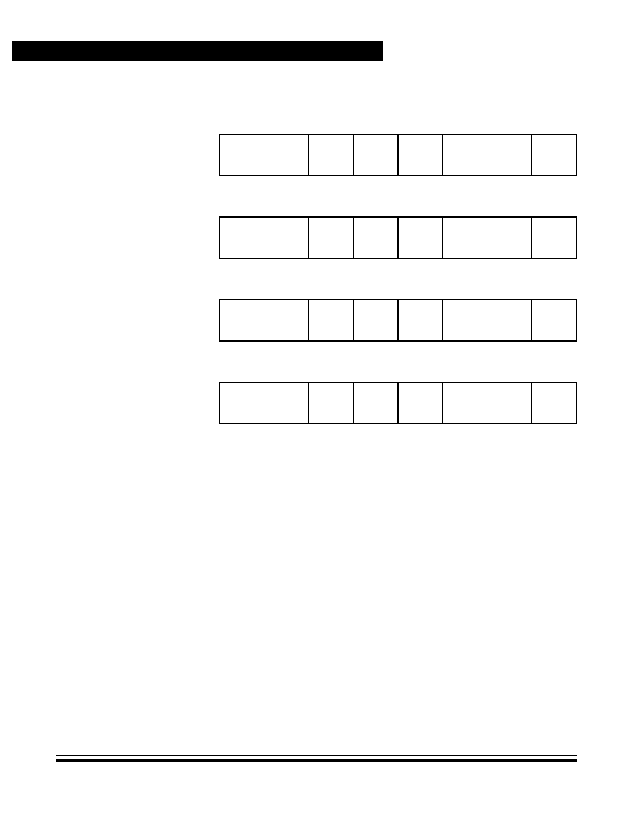
Technical Data
M68HC11K Family
198
Timing System
MOTOROLA
Timing System
All output compare registers are 16-bit read-write. Any of these registers
can be used as a storage location if it is not used for output compare or
input capture.
Address: $001A-- TOC3 (High)
Read:
Bit 15
Bit 14
Bit 13
Bit 12
Bit 11
Bit 10
Bit 9
Bit 8
Write:
Reset:
1
1
1
1
1
1
1
1
Address: $001B -- TOC3 (Low)
Read:
Bit 7
Bit 6
Bit 5
Bit 4
Bit 3
Bit 2
Bit 1
Bit 0
Write:
Reset:
1
1
1
1
1
1
1
1
Address: $001C-- TOC4 (High)
Read:
Bit 15
Bit 14
Bit 13
Bit 12
Bit 11
Bit 10
Bit 9
Bit 8
Write:
Reset:
1
1
1
1
1
1
1
1
Address: $001D -- TOC4 (Low)
Read:
Bit 7
Bit 6
Bit 5
Bit 4
Bit 3
Bit 2
Bit 1
Bit 0
Write:
Reset:
1
1
1
1
1
1
1
1
Bit 7
6
5
4
3
2
1
Bit 0
Figure 9-13. Timer Output Compare
Registers (TOC1�TOC4) (Continued)
Timing System
Output Compare (OC)
M68HC11K Family
Technical Data
MOTOROLA
Timing System
199
9.6.2 Timer Input Capture 4/Output Compare 5 Register
Functions as the output compare register for OC5 when PA3 is
configured for output compare 5. This register is 16-bit read-write. It can
be used as a storage location if it is not used for output compare or input
capture.
9.6.3 Timer Interrupt Flag 1 Register
Clear each flag by writing a 1 to the corresponding bit position.
OCxF -- Output Compare x Flag
Set each time the counter matches output compare x value.
I4/O5F -- Input Capture 4/Output Compare 5 Flag
Set each time the counter matches output compare 5 value if OC5 is
enabled.
Bit 7
6
5
4
3
2
1
Bit 0
Address: $001E -- TI4/O5 (High)
Read:
Bit 15
Bit 14
Bit 13
Bit 12
Bit 11
Bit 10
Bit 9
Bit 8
Write:
Reset:
1
1
1
1
1
1
1
1
Address: $001F -- TI4/O5 (Low)
Read:
Bit 7
Bit 6
Bit 5
Bit 4
Bit 3
Bit 2
Bit 1
Bit 0
Write:
Reset:
1
1
1
1
1
1
1
1
Figure 9-14. Timer Input Capture 4/Output
Compare 5 Register (TI4/O5)
Address: $0023
Bit 7
6
5
4
3
2
1
Bit 0
Read:
OC1F
OC2F
OC3F
OC4F
I4/O5F
IC1F
IC2F
IC3F
Write:
Reset:
0
0
0
0
0
0
0
0
Figure 9-15. Timer Interrupt Flag 1 Register (TFLG1)
Technical Data
M68HC11K Family
200
Timing System
MOTOROLA
Timing System
9.6.4 Timer Interrupt Mask 1 Register
Bits in TMSK1 correspond bit for bit with flag bits in TFLG1.
OC1I�OC4I -- Output Compare x Interrupt Enable Bits
If the OCxI enable bit is set when the OCxF flag bit is set, a hardware
interrupt sequence is requested.
I4/O5I -- Input Capture 4 or Output Compare 5 Interrupt Enable Bit
If I4/O5I is set when OC5 is enabled and the I4/O5F flag bit is set, a
hardware interrupt sequence is requested.
9.6.5 Timer Control 1 Register
OM[2:5] and OL[2:5] -- Output Mode and Output Level Bits
Use these bit pairs as indicated in
Table 9-4
to specify the action
taken after a successful OCx compare.
Address: $0022
Bit 7
6
5
4
3
2
1
Bit 0
Read:
OC1I
OC2I
OC3I
OC4I
I4/O5I
IC1I
IC2I
IC3I
Write:
Reset:
0
0
0
0
0
0
0
0
Figure 9-16. Timer Interrupt Mask 1 Register (TMSK1)
Address: $0020
Bit 7
6
5
4
3
2
1
Bit 0
Read:
OM2
OL2
OM3
OL3
OM4
OL4
OM5
OL5
Write:
Reset:
0
0
0
0
0
0
0
0
Figure 9-17. Timer Control Register 1 (TCTL1)
Timing System
Output Compare (OC)
M68HC11K Family
Technical Data
MOTOROLA
Timing System
201
9.6.6 Timer Compare Force Register
The CFORC register allows forced early compares. Writing a 1 to any bit
of FOC[1:5] forces the programmed pin actions for the corresponding
OC channel to occur at the next timer count transition after the write to
CFORC. The action taken as a result of a forced compare is identical to
the action taken when a match between the OCx register and the
free-running counter occurs, except that the corresponding interrupt and
status flag bits are not set.
CFORC should not be applied to an output compare function that is
programmed to toggle its output on a successful compare because a
normal compare that occurs immediately before or after the force can
result in an undesirable operation.
FOC[1:5] -- Force Output Comparison Bits
0 = No action taken
1 = Output x action occurs at the next timer count transition
Table 9-4. Timer Output Compare Actions
OMx
OLx
Action Taken on Successful Compare
0
0
Timer disconnected from output pin logic
0
1
Toggle OCx output line
1
0
Clear OCx output line to 0
1
1
Set OCx output line to 1
Address: $000B
Bit 7
6
5
4
3
2
1
Bit 0
Read:
FOC1
FOC2
FOC3
FOC4
FOC5
0
0
0
Write:
Reset:
0
0
0
0
0
0
0
0
Figure 9-18. Timer Compare Force Register (CFORC)

Technical Data
M68HC11K Family
202
Timing System
MOTOROLA
Timing System
9.6.7 Output Compare 1 Mask Register
OC1M specifies which bits of port A will respond to a successful
compare for output capture 1. The bits of the OC1M[7:3] register
correspond to PA[7:3].
OC1M[7:3] -- Output Compare 1 Masks
0 = OC1 is disabled at the corresponding PA pin.
1 = OC1 is enabled at the corresponding PA pin.
9.6.8 Output Compare 1 Data Register
Use this register in conjunction with OC1M to specify the data that is to
drive the affected pin of port A after a successful OC1 compare. When a
successful OC1 compare occurs, a data bit in OC1D is stored in the
corresponding bit of port A for each bit that is set in OC1M.
Address: $000C
Bit 7
6
5
4
3
2
1
Bit 0
Read:
OC1M7
OC1M6
OC1M5
OC1M4
OC1M3
0
0
0
Write:
Reset:
0
0
0
0
0
0
0
0
Figure 9-19. Output Compare 1 Mask Register (OC1M)
Address: $000D
Bit 7
6
5
4
3
2
1
Bit 0
Read:
OC1D7
OC1D6
OC1D5
OC1D4
OC1D3
0
0
0
Write:
Reset:
0
0
0
0
0
0
0
0
Figure 9-20. Output Compare 1 Data Register (OC1D)
Timing System
Pulse Accumulator (PA)
M68HC11K Family
Technical Data
MOTOROLA
Timing System
203
OC1D[7:3] -- Output Compare Data Bits
0 = Corresponding port A pin is cleared on successful OC1
compare if the corresponding OC1M bit is set.
1 = Corresponding port A pin is set on successful OC1 compare if
the corresponding OC1M bit is set.
9.7 Pulse Accumulator (PA)
The pulse accumulator can be used either to count events or measure
the duration of a particular event. In event counting mode, the pulse
accumulator's 8-bit counter increments each time a specified edge is
detected on the pulse accumulator input pin, PA7. The maximum
clocking rate for this mode is E clock divided by two. In gated time
accumulation mode, an internal clock increments the 8-bit counter at a
rate of E clock divided by 64 while the input at PA7 remains at a
predetermined logic level.
Table 9-5
shows pulse accumulator clock
periods for three common crystal frequencies.
Figure 9-21
is a block diagram of the pulse accumulator.
Table 9-5. Pulse Accumulator Timing
EXTAL Frequencies
EXTAL Freq.
8.0 MHz
12.0 MHz
16.0 MHz
20.0 MHz
24.0 MHz
Other
EXTAL
E Clock Freq.
2.0 MHz
3.0 MHz
4.0 MHz
5.0 MHz
6.0 MHz
EXTAL
�
Maximum event
counting frequency
1.0 MHz
1.5 MHz
2.0 MHz
2.5 MHz
3.0 MHz
E
�
2
Gated mode count
resolution
32.0
�
s
21.3
�
s
16.0
�
s
12.8
�
s
10.7
�
s
2
6
�
E
Gated mode count
overflow
8.192
�
s
5.461
�
s
4.096
�
s
3.277
�
s
2.731
�
s
2
14
�
E
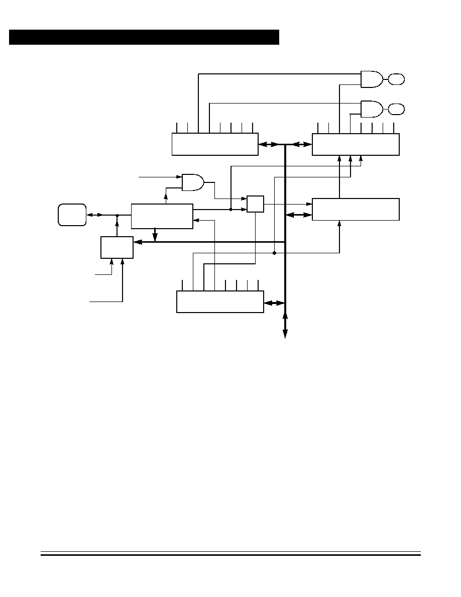
Technical Data
M68HC11K Family
204
Timing System
MOTOROLA
Timing System
Figure 9-21. Pulse Accumulator
Registers involved in pulse accumulator operation include:
�
Data direction register A (DDRA)
�
Pulse accumulator control register (PACTL)
�
Timer interrupt mask 2 register (TMSK2)
�
Timer interrupt flag 2 (TFLG2)
�
Pulse accumulator count register (PACNT)
PACNT
8-BIT COUNTER
2:1
MUX
PA7/
ENABLE
OVERFLOW
1
INTERRUPT
REQUESTS
INTERNAL
DATA BUS
INPUT BUFFER
AND
EDGE DETECTION
PACTL
TFLG2
TMSK2
PA
OVI
PA
I
I
PA
EN
PA
M
O
D
PE
D
G
E
PAOVF
PA
I
F
OUTPUT
BUFFER
PAI EDGE
PAEN
E
�
64 CLOCK
FROM MAIN TIMER
PAI/OC1
FROM
MAIN TIMER
OC1
PAEN
2
CLOCK
FROM
STATUS FLAGS
INTERRUPT ENABLES
CONTROL
DDA7
Timing System
Pulse Accumulator (PA)
M68HC11K Family
Technical Data
MOTOROLA
Timing System
205
9.7.1 Port A Data Direction Register
The pulse accumulator uses port A, bit 7 as the PAI input, but the pin can
also be used as general-purpose I/O or as an output compare.
NOTE:
Even when port A, bit 7 is configured as an output, the pin still drives the
input to the pulse accumulator.
DDA7 -- Data Direction Control for Port A, Bit 7
0 = PA7 configured as an input
1 = PA7 configured as an output
9.7.2 Pulse Accumulator Control Register
PAEN -- Pulse Accumulator System Enable Bit
0 = Pulse accumulator disabled
1 = Pulse accumulator enabled
Address: $0001
Bit 7
6
5
4
3
2
1
Bit 0
Read:
DDA7
DDA6
DDA5
DDA4
DDA3
DDA2
DDA1
DDA0
Write:
Reset:
0
0
0
0
0
0
0
0
Figure 9-22. Port A Data Direction Register (DDRA)
Address: $0026
Bit 7
6
5
4
3
2
1
Bit 0
Read:
0
PAEN
PAMOD
PEDGE
0
I4/O5
RTR1
RTR0
Write:
Reset:
0
0
0
0
0
0
0
0
Figure 9-23. Pulse Accumulator Control Register (PACTL)
Technical Data
M68HC11K Family
206
Timing System
MOTOROLA
Timing System
PAMOD -- Pulse Accumulator Mode Bit
0 = Event counter
1 = Gated time accumulation
PEDGE -- Pulse Accumulator Edge Control Bit
In event counting mode, PEDGE selects either the rising or falling
edge of the input at PA7 to increment the pulse accumulator counter.
In gated accumulation mode, PEDGE determines which input level at
PA7 inhibits counter increments from the internal clock.
Table 9-6
shows the relationship between PEDGE and PAMOD.
9.7.3 Timer Interrupt Flag 2 Register
Clear each flag by writing a 1 to the corresponding bit position.
Table 9-6. Pulse Accumulator Edge Control
PAMOD
PEDGE
Action on Clock
0
0
PAI falling edge increments the counter.
0
1
PAI rising edge increments the counter.
1
0
A 0 on PAI inhibits counting.
1
1
A 1 on PAI inhibits counting.
Address: $0025
Bit 7
6
5
4
3
2
1
Bit 0
Read:
TOF
RTIF
PAOVF
PAIF
0
0
0
0
Write:
Reset:
0
0
0
0
0
0
0
0
Figure 9-24. Timer Interrupt Flag 2 (TFLG2)

Timing System
Pulse Accumulator (PA)
M68HC11K Family
Technical Data
MOTOROLA
Timing System
207
9.7.4 Timer Interrupt Mask 2 Register
Bits in TMSK2 correspond bit for bit with flag bits in TFLG2.
PAOVF -- Pulse Accumulator Overflow Flag
The PAOVF status bit is set each time the pulse accumulator count
rolls over from $FF to $00.
PAOVI -- Interrupt Enable Bit
If PAOVI is set, an interrupt request is also generated. If PAOVI is
cleared, pulse accumulator overflow interrupts are inhibited, and
PAOVF must be polled by user software to determine when an
overflow has occurred. In either case, software must clear PAOVF by
writing a 1 to bit 5 in the TFLG2 register.
PAIF -- Pulse Accumulator Input Edge Flag
The PAIF status bit is automatically set each time a selected edge is
detected at the PA7 pin.
PAII -- Interrupt Enable Bit
If PAII is set, an interrupt request is also generated. If PAII is cleared,
pulse accumulator input interrupts are inhibited, and PAIF must be
polled by user software to determine when an input edge has been
detected. In either case, software must clear PAIF by writing a 1 to
bit 5 in the TFLG2 register.
Address: $0024
Bit 7
6
5
4
3
2
1
Bit 0
Read:
TOI
RTII
PAOVI
PAII
0
0
PR1
PR0
Write:
Reset:
0
0
0
0
0
0
0
0
Figure 9-25. Timer Interrupt Mask 2 (TMSK2)

Technical Data
M68HC11K Family
208
Timing System
MOTOROLA
Timing System
9.7.5 Pulse Accumulator Count Register
In event counting mode, PACNT contains the count of external input
events at the PAI input. In gated accumulation mode, PACNT is
incremented by the pulse accumulator's E
�
64 clock when the PAI input
is at the selected level. Counting is synchronized to the internal PH2
clock so that incrementing and reading occur during opposite half cycles.
The counter is not affected by reset and can be read or written to at any
time.
9.8 Real-Time Interrupt (RTI)
The real-time interrupt (RTI) feature generates hardware interrupts at a
fixed periodic rate. The rate is determined by bits RTR[1:0] in the PACTL
register, which further divide a clock running at E
�
2
13
by 1, 2, 4 or 8.
The resulting periods for various common crystal frequencies are shown
in
Table 9-7
.
Every cycle of the RTI clock sets the RTIF bit in timer interrupt flag 2
(TFLG2) register. This flag can be polled to determine when RTI
timeouts occur, or an interrupt can be generated if the RTII bit in the
timer interrupt mask 2 (TMSK2) register is set. After reset, one entire
real-time interrupt period elapses before the RTIF flag is set for the first
time.
The clock source for the RTI function is a free-running clock that cannot
be stopped or interrupted except by reset. The time between successive
RTI timeouts is a constant that is independent of software latencies
Address: $0027
Bit 7
6
5
4
3
2
1
Bit 0
Read:
Bit 7
Bit 6
Bit 5
Bit 4
Bit 3
Bit 2
Bit 1
Bit 0
Write:
Reset:
0
0
0
0
0
0
0
0
Figure 9-26. Pulse Accumulator Count Register (PACNT)

Timing System
Real-Time Interrupt (RTI)
M68HC11K Family
Technical Data
MOTOROLA
Timing System
209
associated with flag clearing and service. For this reason, an RTI period
starts from the previous timeout, not from when RTIF is cleared.
9.8.1 Timer Interrupt Flag 2 Register
Clear each flag by writing a 1 to the corresponding bit position.
RTIF -- Real-Time Interrupt Flag
The RTIF status bit is automatically set to 1 at the end of every RTI
period.
9.8.2 Timer Interrupt Mask 2 Register
Bits in TMSK2 correspond bit for bit with flag bits in TFLG2.
RTII -- Real-time Interrupt Enable Bit
0 = RTIF interrupts disabled
1 = Interrupt requested when RTIF is set to 1
Address: $0025
Bit 7
6
5
4
3
2
1
Bit 0
Read:
TOF
RTIF
PAOVF
PAIF
0
0
0
0
Write:
Reset:
0
0
0
0
0
0
0
0
Figure 9-27. Timer Interrupt Flag 2 Register (TFLG2)
Address: $0024
Bit 7
6
5
4
3
2
1
Bit 0
Read:
TOI
RTII
PAOVI
PAII
0
0
PR1
PR0
Write:
Reset:
0
0
0
0
0
0
0
0
Figure 9-28. Timer Interrupt Mask 2 Register (TMSK2)
Technical Data
M68HC11K Family
210
Timing System
MOTOROLA
Timing System
9.8.3 Pulse Accumulator Control Register
RTR[1:0] -- Real-Time Interrupt Rate Select Bits
These two bits select a divisor (1, 2, 4, or 8) for the E
�
2
13
RTI clock.
Refer to
Table 9-7
.
Address: $0026
Bit 7
6
5
4
3
2
1
Bit 0
Read:
0
PAEN
PAMOD
PEDGE
0
I4/O5
RTR1
RTR0
Write:
Reset:
0
0
0
0
0
0
0
0
Figure 9-29. Pulse Accumulator Control Register (PACTL)
Table 9-7. Real-Time Interrupt Rate versus RTR[1:0]
RTR[1:0]
Rate
XTAL =
12.0 MHz
XTAL = 2
23
XTAL =
8.0 MHz
XTAL =
4.9152 MHz
XTAL =
4.0 MHz
XTAL =
3.6864 MHz
0
0
2
13
�
E
2.730 ms
3.91 ms
4.10 ms
6.67 ms
8.19 ms
8.89 ms
0
1
2
14
�
E
5.461 ms
7.81 ms
8.19 ms
13.33 ms
16.38 ms
17.78 ms
1
0
2
15
�
E
10.92 ms
15.62 ms
16.38 ms
26.67 ms
32.77 ms
35.56 ms
1
1
2
16
�
E
21.84 ms
31.25 ms
32.77 ms
53.33 ms
65.54 ms
71.11 ms
E =
3.0 MHz
2.1 MHz
2.0 MHz
1.2288 MHz
1.0 MHz
921.6 kHz

Timing System
Pulse-Width Modulator (PWM)
M68HC11K Family
Technical Data
MOTOROLA
Timing System
211
9.9 Pulse-Width Modulator (PWM)
Four 8-bit pulse-width modulation channels are available in the
M68HC11K Family devices. They are output on port H pins 3�0. Pairs of
channels can be concatenated to produce 16-bit outputs. Three
programmable clocks and a flexible clock selection scheme provide a
wide range of frequencies.
The 8-bit mode with E = 4 MHz can produce waveforms from 40 kHz at
1 percent duty cycle resolution to less than 10 Hz at 0.4 percent duty
cycle resolution. In 16-bit mode, a duty cycle resolution down to 15 parts
per million can be achieved (at a frequency of 60 Hz). At 1 kHz, the duty
cycle resolution is 250 ppm.
9.9.1 PWM System Description
Figure 9-30
shows a block diagram of the PWM system. Each of four
channels is enabled by bit PWENx in the PWEN register. Each channel
has an 8-bit counter (PWCNTx), a period register (PWPERx), and a duty
cycle register (PWDTYx). The counter is driven by one of three
user-scaled clock sources -- clock A, B, or S -- selected by the
pulse-width channel select (PCLKx) bit in the pulse-width modulation
timer polarity (PWPOL) register.
A pulse-width modulation period begins when the counter matches the
value stored in the period register. When this happens, a logic value
determined by the polarity bit (PPOLx) in the PWPOL register is driven
on the associated port H output pin, and the counter is reset to 0. When
the counter matches the number stored in the duty cycle register, the
output reverses polarity. The period and duty cycle registers are double
buffered so they can be changed without disturbing the current
waveform. A new period or duty cycle can be forced by writing to the
period (PWPERx) or duty cycle register (PWDTYx) and then to the
counter (PWCNTx). Writing to the counter always resets it to 0.
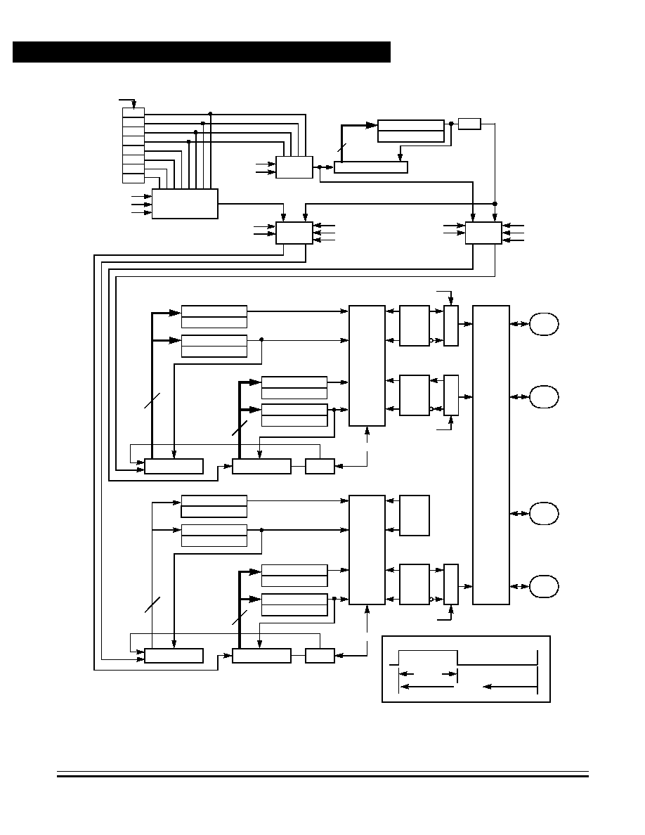
Technical Data
M68HC11K Family
212
Timing System
MOTOROLA
Timing System
Figure 9-30. Pulse-Width Modulation Timer Block Diagram
S
Q
R
Q
�1
�2
�4
�8
�16
�32
�64
�128
SELECT
PCKB1
PCKB2
PCKB3
SELECT
PCKA1
PCKA2
8-BIT COUNTER
8-BIT COMPARE
PWSCAL
=
8
�
2
RESET
CLOCK S
CLOCK B
CLOCK
SELECT
CLOCK A
PWEN1
CLOCK
SELECT
PWEN2
CON12
PCLK1
PCLK2
E CLOCK
CNT4
CNT3
CNT2
CNT1
S
Q
R
Q
S
Q
R
Q
S
R
CONTROL
16-BIT
PWM
CONTROL
16-BIT
PWM
PW1
PW2
PW3
PW4
M
U
X
M
U
X
M
U
X
PORT H
PIN
CONTROL
BIT 0
BIT 1
BIT 2
BIT 3
8-BIT COMPARE
PWDTY2
=
8-BIT COMPARE
PWPER2
=
8-BIT COMPARE
PWDTY4
=
8-BIT COMPARE
PWPER4
=
8-BIT COMPARE
PWDTY1
=
8-BIT COMPARE
PWPER1
=
8-BIT COMPARE
PWDTY3
=
8-BIT COMPARE
PWPER3
=
RESET
PWCNT2
CARRY
PWCNT1
RESET
PWCNT4
CARRY
PWCNT3
8
8
8
8
CON12
CON34
PPOL1
PPOL3
PPOL4
PPOL2
PWPER
PWDTY
PCLK3
PCLK4
PWEN3
PWEN4
CON12
RESET
RESET

Timing System
Pulse-Width Modulator (PWM)
M68HC11K Family
Technical Data
MOTOROLA
Timing System
213
The three clocks are derived from the E clock by writing to registers
which determine their scaling factors. The clock A frequency is equal to
E divided by 1, 2, 4, or 8, depending on which bits (PCKA[2:1]) in the
PWCLK register are set. The clock B frequency is equal to the E clock
divided by a power of two determined by bits PCKB[3:1] in the PWCLK
register. Clock S is derived by dividing clock A by the integer (1 to 256)
stored in the PWSCAL register, then by two.
Two channels can be concatenated by setting the appropriate bit
(CON34 or CON12) in the PWCLK register. In this mode, the clock
source is determined by the low-order channel, which is channel two in
CON12 and channel four in CON34. The output is also placed on the pin
associated with the low-order channels, so when two channels are
concatenated the pin associated with the high-order channel (PH0
and/or PH2) can be used for GPIO. A read of the high-order byte causes
the low-order byte to be latched for one cycle to guarantee that
double-byte reads are accurate. A write to the low-order byte of the
counter causes reset of the entire counter. A write to the high-order byte
of the counter has no effect.
9.9.2 Pulse-Width Modulation Control Registers
The PWM control registers are described here.
9.9.2.1 Pulse-Width Modulation Timer Clock Select Register
Address: $0060
Bit 7
6
5
4
3
2
1
Bit 0
Read:
CON34
CON12
PCKA2
PCKA1
0
PCKB3
PCKB2
PCKB1
Write:
Reset:
0
0
0
0
0
0
0
0
Figure 9-31. Pulse-Width Modulation Timer Clock Select (PWCLK)

Technical Data
M68HC11K Family
214
Timing System
MOTOROLA
Timing System
CON34 -- Concatenate Channels 3 and 4 Bit
Channel 3 is the high-order byte, and channel 4 (port H, bit 3) is
output.
0 = Channels 3 and 4 are separate 8-bit PWMs.
1 = Channels 3 and 4 are concatenated to create one 16-bit PWM.
CON12 -- Concatenate Channels 1 and 2 Bit
Channel 1 is the high-order byte, and channel 2 (port H, bit 1) is
output.
0 = Channels 1 and 2 are separate 8-bit PWMs.
1 = Channels 1 and 2 are concatenated to create one 16-bit PWM.
PCKA[2:1] -- Prescaler for Clock A Bits
These bits select the frequency for clock A as shown in
Table 9-8
.
PCKB[3:1] -- Prescaler for Clock B Bits
These bits select the frequency for clock B as shown in
Table 9-9
.
Table 9-8. Clock A Prescaler
PCKA[2:1]
Clock A Frequency
0
0
E
0
1
E/2
1
0
E/4
1
1
E/8
Table 9-9. Clock B Prescaler
PCKB[3:1]
Clock B Frequency
0
0
0
E
0
0
1
E/2
0
1
0
E/4
0
1
1
E/8
1
0
0
E/16
1
0
1
E/32
1
1
0
E/64
1
1
1
E/128
Timing System
Pulse-Width Modulator (PWM)
M68HC11K Family
Technical Data
MOTOROLA
Timing System
215
9.9.2.2 Pulse-Width Modulation Timer Polarity Register
PCLK[4:3] -- Pulse-Width Channel 4, 3 Clock Select Bits
0 = Clock B is source.
1 = Clock S is source.
PCLK[2:1] -- Pulse-Width Channel 2, 1 Clock Select Bits
0 = Clock A is source.
1 = Clock S is source.
PPOL[4:1] -- Pulse-Width Channel x Polarity Bits
0 = PWM channel x output is low at the beginning of the clock cycle
and goes high when duty count is reached.
1 = PWM channel x output is high at the beginning of the clock
cycle and goes low when duty count is reached.
9.9.2.3 Pulse-Width Modulation Timer Prescaler Register
Scaled clock S is generated by dividing clock A by the value in PWSCAL,
then dividing the result by two. If PWSCAL = $00, the divisor is 256, then
two.
Address: $0061
Bit 7
6
5
4
3
2
1
Bit 0
Read:
PCLK4
PCLK3
PCLK2
PCLK1
PPOL4
PPOL3
PPOL2
PPOL1
Write:
Reset:
0
0
0
0
0
0
0
0
Figure 9-32. Pulse-Width Modulation Timer
Polarity Register (PWPOL)
Address: $0062
Bit 7
6
5
4
3
2
1
Bit 0
Read:
Bit 7
Bit 6
Bit 5
Bit 4
Bit 3
Bit 2
Bit 1
Bit 0
Write:
Reset:
0
0
0
0
0
0
0
0
Figure 9-33. Pulse-Width Modulation Timer
Prescaler Register (PWSCAL)
Technical Data
M68HC11K Family
216
Timing System
MOTOROLA
Timing System
9.9.2.4 Pulse-Width Modulation Timer Enable Register
TPWSL -- PWM Scaled Clock Test Bit -- factory use only; only
accessible in special test mode
0 = Normal operation
1 = Clock S is output to PWSCAL register (test only)
DISCP -- Disable Compare Scaled E-Clock Bit -- factory use only; only
accessible in special test mode
0 = Normal operation
1 = Match of period does not reset associated count register (test
only)
PWEN[4:1] -- Pulse-Width Enable for Channels [4:1] Bits
0 = Channel disabled
1 = Channel enabled at port H bits [3:0]
Address: $0063
Bit 7
6
5
4
3
2
1
Bit 0
Read:
TPWSL
DISCP
0
0
PWEN4
PWEN3
PWEN2
PWEN1
Write:
Reset:
0
0
0
0
0
0
0
0
Figure 9-34. Pulse-Width Modulation Timer
Enable Register (PWEN)

Timing System
Pulse-Width Modulator (PWM)
M68HC11K Family
Technical Data
MOTOROLA
Timing System
217
9.9.2.5 Pulse-Width Modulation Timer Counters 1 to 4 Registers
Each counter resets to 0 when it is written and can be read at any time.
Bit 7
6
5
4
3
2
1
Bit 0
Address: $0064 -- PWCNT1
Read:
Bit 7
Bit 6
Bit 5
Bit 4
Bit 3
Bit 2
Bit 1
Bit 0
Write:
Reset:
0
0
0
0
0
0
0
0
Address: $0065 -- PWCNT2
Read:
Bit 7
Bit 6
Bit 5
Bit 4
Bit 3
Bit 2
Bit 1
Bit 0
Write:
Reset:
0
0
0
0
0
0
0
0
Address: $0066 -- PWCNT3
Read:
Bit 7
Bit 6
Bit 5
Bit 4
Bit 3
Bit 2
Bit 1
Bit 0
Write:
Reset:
0
0
0
0
0
0
0
0
Address: $0067 -- PWCNT4
Read:
Bit 7
Bit 6
Bit 5
Bit 4
Bit 3
Bit 2
Bit 1
Bit 0
Write:
Reset:
0
0
0
0
0
0
0
0
Figure 9-35. Pulse-Width Modulation Timer
Counters 1 to 4 (PWCNT1 to PWCNT4)

Technical Data
M68HC11K Family
218
Timing System
MOTOROLA
Timing System
9.9.2.6 Pulse-Width Modulation Timer Periods 1 to 4 Registers
Each period register can be read or written at any time. If it is written, the
new period will not take effect until the associated counter is reset by a
match or a write.
Bit 7
6
5
4
3
2
1
Bit 0
Address: $0068 -- PWPER1
Read:
Bit 7
Bit 6
Bit 5
Bit 4
Bit 3
Bit 2
Bit 1
Bit 0
Write:
Reset:
0
0
0
0
0
0
0
0
Address: $0069 -- PWPER2
Read:
Bit 7
Bit 6
Bit 5
Bit 4
Bit 3
Bit 2
Bit 1
Bit 0
Write:
Reset:
0
0
0
0
0
0
0
0
Address: $006A -- PWPER3
Read:
Bit 7
Bit 6
Bit 5
Bit 4
Bit 3
Bit 2
Bit 1
Bit 0
Write:
Reset:
0
0
0
0
0
0
0
0
Address: $006B -- PWPER4
Read:
Bit 7
Bit 6
Bit 5
Bit 4
Bit 3
Bit 2
Bit 1
Bit 0
Write:
Reset:
0
0
0
0
0
0
0
0
Figure 9-36. Pulse-Width Modulation Timer
Periods 1 to 4 (PWPER1 to PWPER4)
Timing System
Pulse-Width Modulator (PWM)
M68HC11K Family
Technical Data
MOTOROLA
Timing System
219
9.9.2.7 Pulse-Width Modulation Timer Duty Cycle 1 to 4 Registers
Each duty cycle register can be read or written at any time. If it is written,
the new duty cycle will not take effect until the associated counter is reset
by a match or a write.
Bit 7
6
5
4
3
2
1
Bit 0
Address: $006C -- PWDTY1
Read:
Bit 7
Bit 6
Bit 5
Bit 4
Bit 3
Bit 2
Bit 1
Bit 0
Write:
Reset:
0
0
0
0
0
0
0
0
Address: $006D -- PWDTY2
Read:
Bit 7
Bit 6
Bit 5
Bit 4
Bit 3
Bit 2
Bit 1
Bit 0
Write:
Reset:
0
0
0
0
0
0
0
0
Address: $006E -- PWDTY3
Read:
Bit 7
Bit 6
Bit 5
Bit 4
Bit 3
Bit 2
Bit 1
Bit 0
Write:
Reset:
0
0
0
0
0
0
0
0
Address: $006F -- PWDTY4
Read:
Bit 7
Bit 6
Bit 5
Bit 4
Bit 3
Bit 2
Bit 1
Bit 0
Write:
Reset:
0
0
0
0
0
0
0
0
Figure 9-37. Pulse-Width Modulation Timer
Duty Cycle 1 to 4 (PWDTY1 to PWDTY4)

Technical Data
M68HC11K Family
220
Timing System
MOTOROLA
Timing System

M68HC11K Family
Technical Data
MOTOROLA
Analog-to-Digital (A/D) Converter
221
Technical Data -- M68HC11K Family
Section 10. Analog-to-Digital (A/D) Converter
10.1 Contents
10.2
Introduction . . . . . . . . . . . . . . . . . . . . . . . . . . . . . . . . . . . . . . . 221
10.3
Functional Description . . . . . . . . . . . . . . . . . . . . . . . . . . . . . . 222
10.3.1
Multiplexer . . . . . . . . . . . . . . . . . . . . . . . . . . . . . . . . . . . . .223
10.3.2
Analog Converter . . . . . . . . . . . . . . . . . . . . . . . . . . . . . . . . 223
10.3.3
Result Registers . . . . . . . . . . . . . . . . . . . . . . . . . . . . . . . . .223
10.3.4
Digital Control . . . . . . . . . . . . . . . . . . . . . . . . . . . . . . . . . . . 224
10.4
A/D Control/Status Registers . . . . . . . . . . . . . . . . . . . . . . . . . 226
10.4.1
System Configuration Options Register . . . . . . . . . . . . . . . 226
10.4.2
A/D Control/Status Register . . . . . . . . . . . . . . . . . . . . . . . . 227
10.4.3
Analog-to-Digital Converter Result Registers. . . . . . . . . . . 229
10.5
Design Considerations . . . . . . . . . . . . . . . . . . . . . . . . . . . . . . 230
10.5.1
A/D Input Pins . . . . . . . . . . . . . . . . . . . . . . . . . . . . . . . . . . 230
10.5.2
Operation in Stop and Wait Modes . . . . . . . . . . . . . . . . . .230
10.2 Introduction
The analog-to-digital (A/D) system in M68HC11 microcontrollers is an
8-channel, 8-bit, multiplexed input converter. It employs a successive
approximation technique with an all-capacitive charge redistribution
system that does not require external sample-and-hold circuits. A/D
converter timing can be synchronized either to the E clock or an internal
resistor-capacitor (RC) oscillator. Separate power supply inputs, AV
DD
and AV
SS
, allow independent bypassing for noise immunity.
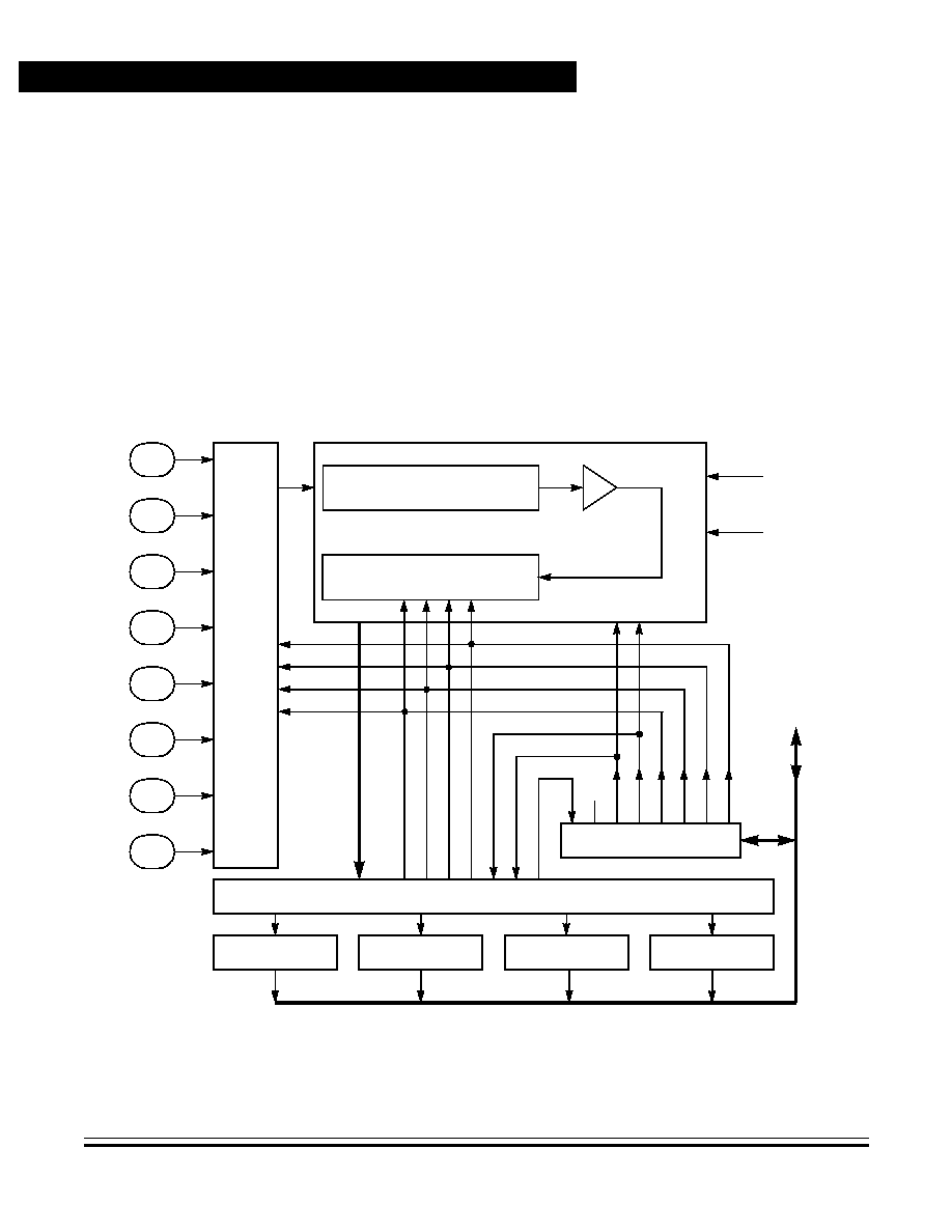
Technical Data
M68HC11K Family
222
Analog-to-Digital (A/D) Converter
MOTOROLA
Analog-to-Digital (A/D) Converter
10.3 Functional Description
The A/D converter system consists of four functional blocks as shown in
Figure 10-1
:
�
Multiplexer
�
Analog converter
�
Result storage
�
Digital control
Figure 10-1. A/D Converter Block Diagram
PE0
AN0
V
RH
V
RL
PE1
AN1
PE2
AN2
PE3
AN3
PE4
AN4
PE5
AN5
PE6
AN6
PE7
AN7
RESULT REGISTER INTERFACE
ADCTL
SC
AN
MUL
T
CD
CC
CB
CA
CCF
RESULT
ADR1
ADR2
ADR3
ADR4
8-BIT CAPACITIVE DAC
WITH SAMPLE AND HOLD
SUCCESSIVE APPROXIMATION
REGISTER AND CONTROL
ANALOG
MUX
INTERNAL
DATA BUS

Analog-to-Digital (A/D) Converter
Functional Description
M68HC11K Family
Technical Data
MOTOROLA
Analog-to-Digital (A/D) Converter
223
10.3.1 Multiplexer
The multiplexer selects which of the eight analog inputs at port E will be
converted. There are also three internal reference levels which can be
multiplexed to the converter for system testing. Input selection is
controlled by the value of bits CD:CA in the A/D control register
(ADCTL).
The V
RH
and V
RL
pins provide inputs for the A/D system reference
voltage. An input voltage equal to V
RL
converts to $00 and an input
voltage equal to V
RH
converts to $FF (full scale), with no overflow
indication. For ratiometric conversions of this type, the source of
each analog input should use V
RH
as the supply voltage and be
referenced to V
RL
.
10.3.2 Analog Converter
The conversion block contains a digital-to-analog capacitor (DAC) array,
a comparator, and a successive approximation register (SAR). When an
analog input is sampled for conversion, an analog switch connects the
input to the DAC array. This series of scaled capacitors retains the
sample for the duration of the conversion.
A conversion consists of a sequence of eight comparison operations.
Each comparison determines one bit of the result, starting with the most
significant bit (MSB). During each comparison, analog switches connect
different elements of the DAC array to the comparator. The output of the
comparator is stored in the next bit in the successive approximation
register. When a conversion sequence is complete, the contents of the
SAR are transferred to the appropriate result register.
10.3.3 Result Registers
The A/D conversion sequence begins one E-clock cycle after a write to
the analog-to-digital control/status register (ADCTL). Converter
operations are performed in sequences of four conversions each. Each
conversion result in a sequence is stored in one of the four result
registers, ADR[4:1]. The conversion complete flag (CCF) in the ADCTL
Technical Data
M68HC11K Family
224
Analog-to-Digital (A/D) Converter
MOTOROLA
Analog-to-Digital (A/D) Converter
register is set after the fourth conversion in a sequence to signal the
availability of data in the result registers.The result registers are written
during a portion of the system clock cycle when reads do not occur, so
there is no conflict. A conversion sequence can repeat continuously or
stop after one iteration.
Figure 10-2
shows the timing of a typical
sequence. In this example, synchronization is referenced to the system
E clock.
Figure 10-2. A/D Conversion Sequence
10.3.4 Digital Control
In addition to the conversion complete status flag, ADCTL bits select
single or continuous conversions, whether conversions are performed
on single or multiple channels, and the analog input(s) to be converted.
Single or continuous conversions are selected by the SCAN bit. Clearing
the SCAN bit selects the single conversion option, in which results are
written to each of the four result registers one time. The first result is
stored in A/D result register 1 (ADR1), and the fourth result is stored in
ADR4. All conversion activity is then halted until the ADCTL register is
written again. In the continuous mode (SCAN =1), conversion activity
does not stop. The fifth conversion is stored in register ADR1
(overwriting the first conversion result), the sixth conversion overwrites
ADR2, and so on.
0
32
64
96
128 -- E CYCLES
SAMPLE ANALOG INPUT
SUCCESSIVE APPROXIMATION SEQUENCE
MSB
4
CYCLES
BIT 6
2
CYC
BIT 5
2
CYC
BIT 4
2
CYC
BIT 3
2
CYC
BIT 2
2
CYC
BIT 1
2
CYC
LSB
2
CYC
2
CYC
END
R
EPE
AT
SE
QU
EN
C
E
,
SC
AN
=
1
SET
C
C
F
L
A
G
CONVERT FIRST
CHANNEL, UPDATE
ADR1
CONVERT SECOND
CHANNEL, UPDATE
ADR2
CONVERT THIRD
CHANNEL, UPDATE
ADR3
CONVERT FOURTH
CHANNEL, UPDATE
ADR4
12 E CYCLES
WR
ITE
TO
A
DCT
L
E CLOCK
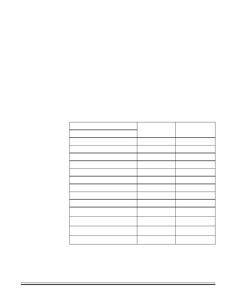
Analog-to-Digital (A/D) Converter
Functional Description
M68HC11K Family
Technical Data
MOTOROLA
Analog-to-Digital (A/D) Converter
225
The MULT bit in ADCTL determines whether one or four channels are
converted. When MULT = 0, one channel is converted. The selected
channel is sampled and the conversion results are written to ADR1; the
same channel is sampled again, and the conversion results are stored
in ADR2, and so on. In continuous mode, the same channel continues to
be sampled and converted. Setting the MULT bit converts four different
channels; each result register contains the conversion result of a
different channel. In continuous mode, the same four channels are
converted in each sequence.
ADCTL bits [3:0] select the particular channel(s) to be converted. See
Table 10-1
.
Table 10-1. A/D Converter Channel Selection
Channel Select Control Bits
Channel Signal
Result Location
When MULT = 1
CD:CC:CB:CA
0000
AN0
ADR1
0001
AN1
ADR2
0010
AN2
ADR3
0011
AN3
ADR4
0100
AN4
ADR1
0101
AN5
ADR2
0110
AN6
ADR3
0111
AN7
ADR4
10XX
Reserved
--
1100
V
RH
(1)
1. Used for factory testing
ADR1
1101
V
RL
(1)
ADR2
1110
(V
RH
)/2
(1)
ADR3
1111
Reserved
(1)
ADR4

Technical Data
M68HC11K Family
226
Analog-to-Digital (A/D) Converter
MOTOROLA
Analog-to-Digital (A/D) Converter
10.4 A/D Control/Status Registers
The registers involved in A/D operation include OPTION, ADCTL, and
the four result registers ADR[1:4].
NOTE:
Throughout this manual, the registers are discussed by function. In the
event that not all bits in a register are referenced, the bits that are not
discussed are shaded.
10.4.1 System Configuration Options Register
Bit 7 in the system configuration options register (OPTION), ADPU,
enables the A/D converter system. Setting ADPU applies power to the
A/D circuitry, including the charge pump that drives the analog switches.
Clearing ADPU removes power from the A/D system.
The gates of analog switches in the multiplexer are driven by a charge
pump that develops between seven and eight volts. The high gate
voltage assures low source-to-drain impedance for the analog signals.
Both the charge pump and the comparator circuits require up to 100
�
s
to stabilize after setting the ADPU bit.
The CSEL bit (bit 6) determines whether the A/D converter uses the
system E clock or an internal RC oscillator for synchronization. It is
cleared out of reset, selecting the E clock. This is the preferred setting at
normal operating frequencies because all switching and comparator
operations are synchronized to the main MCU clocks. This allows the
comparator output to be sampled at relatively quiet portions of the MCU
clock cycles.
When the E clock frequency is less than 750 kHz, charge leakage in the
capacitor array can cause errors. In this case, set the CSEL bit to select
the internal oscillator, which usually runs at about 2 MHz. The additional
error introduced by the asynchronous oscillator is about � 1/2 LSB (least
significant bit), which is usually less than that incurred by a slow clock.
Analog-to-Digital (A/D) Converter
A/D Control/Status Registers
M68HC11K Family
Technical Data
MOTOROLA
Analog-to-Digital (A/D) Converter
227
ADPU -- A/D Power-up
0 = A/D powered down
1 = A/D powered up
CSEL -- Clock Select
0 = A/D and EEPROM use system E clock.
1 = A/D and EEPROM use internal RC clock.
10.4.2 A/D Control/Status Register
All bits in this register can be read or written except bit 7, which is a
read-only status indicator, and bit 6, which always reads as 0. Writing to
ADCTL initiates a conversion, aborting any conversion in progress.
Address: $0039
Bit 7
6
5
4
3
2
1
Bit 0
Read:
ADPU
CSEL
IRQE
DLY
(1)
CME
FCME
CR1
CR0
Write:
Reset:
0
0
0
1
0
0
0
0
1. DLY can be written only once in the first 64 cycles out of reset in normal modes or at any
time in special modes.
Figure 10-3. System Configuration Options Register (OPTION)
Address: $0030
Bit 7
6
5
4
3
2
1
Bit 0
Read:
CCF
SCAN
MULT
CD
CC
CB
CA
Write:
Reset:
0
0
U
U
U
U
U
U
= Unimplemented
U = Unaffected by reset
Figure 10-4. Analog-to-Digital Control/Status Register (ADCTL)

Technical Data
M68HC11K Family
228
Analog-to-Digital (A/D) Converter
MOTOROLA
Analog-to-Digital (A/D) Converter
CCF -- Conversions Complete Flag
Set when all four A/D result registers contain valid conversion results.
Cleared when the ADCTL register is overwritten, starting a new
conversion sequence. In continuous mode, CCF is set at the end of
the first conversion sequence.
SCAN -- Continuous Scan Control Bit
0 = Conversion process stops after each of the four result registers
is written.
1 = Conversions are performed continuously.
MULT -- Multiple Channel/Single Channel Control Bit
0 = A single channel specified by the four channel select bits
CD:CA is sampled and converted four times.
1 = Each of four channels is converted and the results written to a
different result register.
NOTE:
When the multiple-channel continuous scan mode is used, extra care is
needed in the design of circuitry driving the A/D inputs. The charge on
the capacitive DAC array before the sample time is related to the voltage
on the previously converted channel. A charge share situation exists
between the internal DAC capacitance and the external circuit
capacitance. Although the amount of charge involved is small, the rate
at which it is repeated is every 64
�
s for an E clock of 2 MHz. The RC
charging rate of the external circuit must be balanced against this charge
sharing effect to avoid errors in accuracy. Refer to the M68HC11
Reference Manual, Motorola document order number M68HC11RM/AD,
for further information.
CD:CA -- Channel Selects D:A Bits
Refer to
Table 10-1
. In multiple channel mode (MULT = 1), the two
least significant channel select bits (CB and CA) have no meaning
and the CD and CC bits specify which group of four channels is to be
converted.
Analog-to-Digital (A/D) Converter
A/D Control/Status Registers
M68HC11K Family
Technical Data
MOTOROLA
Analog-to-Digital (A/D) Converter
229
10.4.3 Analog-to-Digital Converter Result Registers
These read-only registers hold an 8-bit conversion result. Writes to these
registers have no effect. Data in the A/D converter result registers is valid
when the CCF flag in the ADCTL register is set, indicating a conversion
sequence is complete. If conversion results are needed sooner, refer to
Figure 10-2
, which shows the A/D conversion sequence diagram.
Bit 7
6
5
4
3
2
1
Bit 0
Address: $0031
Analog-to-Digital Result Register 1
Read:
Bit 7
Bit 6
Bit 5
Bit 4
Bit 3
Bit 2
Bit 1
Bit 0
Write:
Reset:
Undefined after reset
Address: $0032
Analog-to-Digital Result Register 2
Read:
Bit 7
Bit 6
Bit 5
Bit 4
Bit 3
Bit 2
Bit 1
Bit 0
Write:
Reset:
Undefined after reset
Address: $0033
Analog-to-Digital Result Register 3
Read:
Bit 7
Bit 6
Bit 5
Bit 4
Bit 3
Bit 2
Bit 1
Bit 0
Write:
Reset:
Undefined after reset
Address: $0034
Analog-to-Digital Result Register 4
Read:
Bit 7
Bit 6
Bit 5
Bit 4
Bit 3
Bit 2
Bit 1
Bit 0
Write:
Reset:
Undefined after reset
= Unimplemented
Figure 10-5. Analog-to-Digital Result Registers (ADR1�ADR4))
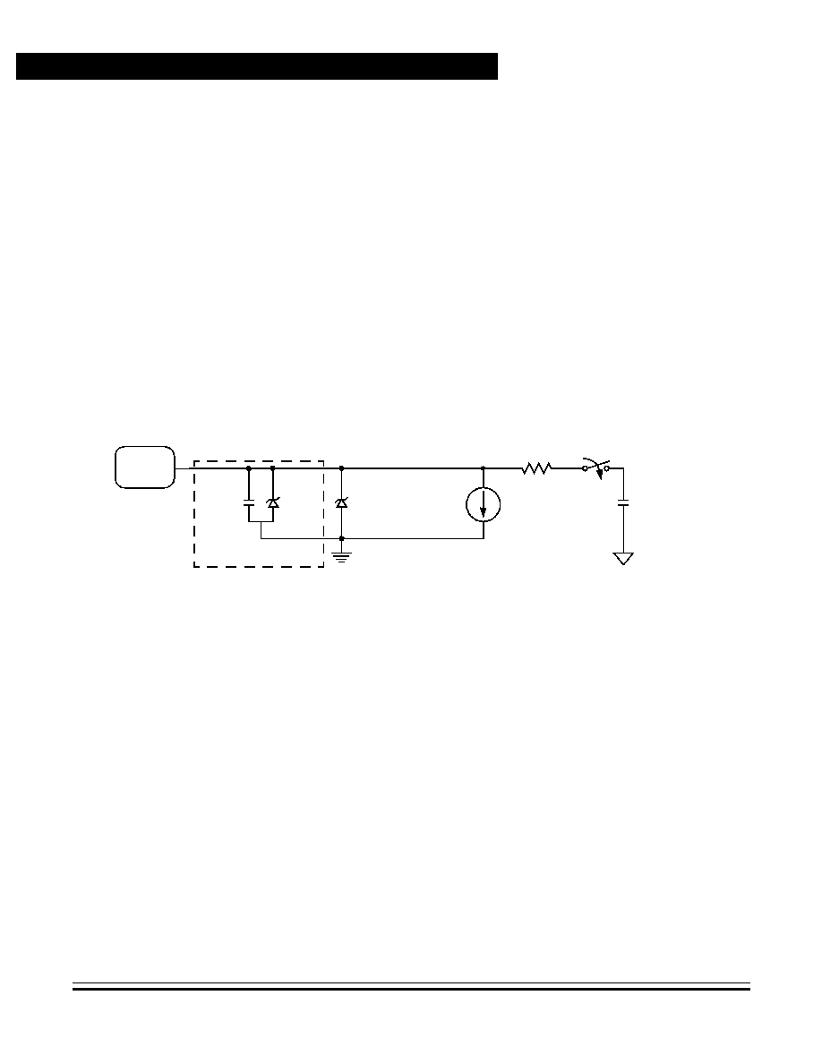
Technical Data
M68HC11K Family
230
Analog-to-Digital (A/D) Converter
MOTOROLA
Analog-to-Digital (A/D) Converter
10.5 Design Considerations
This section discusses design considerations.
10.5.1 A/D Input Pins
Port E pins can also be used as general-purpose digital inputs. Digital
reads of port E pins are not recommended during the sample portion of
an A/D conversion cycle, when the gate signal to the N-channel input is
on. No P-channel devices are directly connected to either input pins or
reference voltage pins, so voltages above V
DD
do not cause a latchup
problem, although current should be limited according to maximum
ratings. Refer to
Figure 10-6
.
Figure 10-6. Electrical Model of an A/D Input Pin (Sample Mode)
10.5.2 Operation in Stop and Wait Modes
If a conversion sequence is in progress when either the stop or wait
mode is entered, the conversion of the current channel is suspended.
When the MCU resumes normal operation, that channel is resampled
and the conversion sequence is resumed. As the MCU exits the wait
mode, the A/D circuits are stable and valid results can be obtained on
the first conversion. However, in stop mode, all analog bias currents are
disabled and it is necessary to allow a stabilization period when leaving
stop mode. If stop mode is exited with a delay (DLY = 1), there is enough
time for these circuits to stabilize before the first conversion. If stop mode
is exited with no delay (DLY bit in OPTION register = 0), allow 10 ms for
the A/D circuitry to stabilize to avoid invalid results.
DIFFUSION/POLY
< 2 pF
COUPLER
400 nA
JUNCTION
LEAKAGE
+ ~20 V
� ~0.7 V
*
Note 1. This analog switch is closed only during the 12-cycle sample time.
V
RL
INPUT
+ ~12 V
� ~0.7 V
PROTECTION
DEVICE
4 k
DUMMY N-CHANNEL
OUTPUT DEVICE
ANALOG
INPUT
PIN
~ 20 pF
DAC
CAPACITANCE
SEE NOTE 1

M68HC11K Family
Technical Data
MOTOROLA
Memory Expansion and Chip Selects
231
Technical Data -- M68HC11K Family
Section 11. Memory Expansion and Chip Selects
11.1 Contents
11.2
Introduction . . . . . . . . . . . . . . . . . . . . . . . . . . . . . . . . . . . . . . . 231
11.3
Memory Expansion . . . . . . . . . . . . . . . . . . . . . . . . . . . . . . . . .232
11.3.1
Memory Size and Address Line Allocation. . . . . . . . . . . . . 232
11.3.2
Control Registers . . . . . . . . . . . . . . . . . . . . . . . . . . . . . . . .234
11.3.2.1
Port G Assignment Register . . . . . . . . . . . . . . . . . . . . . 234
11.3.2.2
Memory Mapping Size Register . . . . . . . . . . . . . . . . . . .235
11.3.2.3
Memory Mapping Window Base Register . . . . . . . . . . . 236
11.3.2.4
Memory Mapping Window Control Registers. . . . . . . . .237
11.4
Chip Selects . . . . . . . . . . . . . . . . . . . . . . . . . . . . . . . . . . . . . . 238
11.4.1
Program Chip Select . . . . . . . . . . . . . . . . . . . . . . . . . . . . . 240
11.4.2
Input/Output Chip Select . . . . . . . . . . . . . . . . . . . . . . . . . . 241
11.4.3
General-Purpose Chip Selects. . . . . . . . . . . . . . . . . . . . . . 242
11.4.3.1
Memory Mapping Size Register . . . . . . . . . . . . . . . . . . .243
11.4.3.2
General-Purpose Chip Select 1 Address Register. . . . .243
11.4.3.3
General-Purpose Chip Select 1 Control Register . . . . . 244
11.4.3.4
General-Purpose Chip Select 2 Address Register. . . . .245
11.4.3.5
General-Purpose Chip Select 2 Control Register . . . . . 245
11.4.4
One Chip Select Driving Another . . . . . . . . . . . . . . . . . . . . 246
11.4.4.1
General-Purpose Chip Select 1 Control Register . . . . . 247
11.4.4.2
General-Purpose Chip Select 2 Control Register . . . . . 247
11.4.5
Clock Stretching . . . . . . . . . . . . . . . . . . . . . . . . . . . . . . . . .248
11.5
Memory Expansion Examples . . . . . . . . . . . . . . . . . . . . . . . . 249
11.2 Introduction
This section provides descriptions of the expanded memory and the chip
selects.

Technical Data
M68HC11K Family
232
Memory Expansion and Chip Selects
MOTOROLA
Memory Expansion and Chip Selects
11.3 Memory Expansion
The M68HC11K Family devices employ a register-based paging
scheme to extend their address range beyond the physical 64-Kbyte
limit of the 16 CPU address lines. Pages are selected using the
expansion address lines XA[18:13] available on port G. This selection
can be facilitated by the chip-select lines on port H, discussed in
11.4 Chip Selects
. The M68HC11KS devices do not provide these
features since they lack the required port G and port H lines. Refer to
Figure 1-2. M68HC11KS Family Block Diagram
.
11.3.1 Memory Size and Address Line Allocation
To access expanded memory, the user first allocates portion(s) of the 64
Kbyte address space, or window(s), through which the CPU will view
external memory. One or two windows can be designated, and the size
of each window can be 0 (disabled), 8, 16, or 32 Kbytes.
Expanded memory is addressed with a combination of the CPU's normal
address lines ADDR[15:0] and the expansion address lines XA[18:13].
The expansion address lines select a memory bank, and the CPU's
normal address lines select a particular location within the bank. The
size of the window(s) and the number of memory banks determine
exactly which expansion address lines are used. The port G assignment
register (PGAR) controls which port G pins function as expanded
address lines. Any port G pins not allocated for memory expansion can
serve as general-purpose input/output (GPIO). When a configuration
uses any of the lower three expansion address lines XA[15:13] they
replace the CPU's equivalent address lines (ADDR[15:13]).
Table 11-1
shows how address and expansion lines are allocated for various
combinations of memory banks and window size.
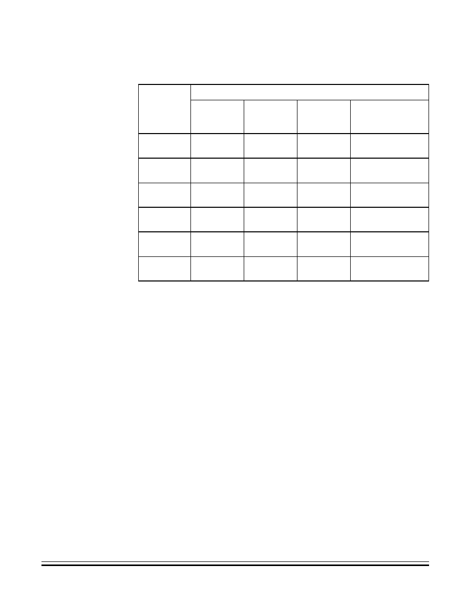
Memory Expansion and Chip Selects
Memory Expansion
M68HC11K Family
Technical Data
MOTOROLA
Memory Expansion and Chip Selects
233
The base address for each window must be an integer multiple of the
window size, with one exception. When the window size is 32 Kbytes,
the base address can be at $4000 as well as the 32-Kbyte multiples
$0000 and $8000.
This special case requires a modification in address line deployment.
Normally, when the bank size is 32 Kbytes and the bank address is
$0000 or $8000, CPU address lines ADDR[14:0] select individual bytes
within the 32-Kbyte space and the ADDR[14:0] pins are connected to
address lines A[14:0] of the memory device. When the base address is
$4000, the CPU address signal ADDR14 must be inverted to allow
32 Kbytes of contiguous memory. To do this, the CPU drives the
inverted ADDR14 signal onto the XA14 pin when the window is active,
and the non-inverted CPU ADDR14 signal onto the XA14 pin when the
window is not active. Therefore, address 14 of the memory device must
be connected to expansion line XA14 rather than normal address line
ADDR14.
If the two memory windows overlap, window 1 has priority, and only the
portion of window 2 that does not overlap window 1 remains active. If a
Table 11-1. CPU Address and Address Expansion Signals
Number
of Banks
Window Size
8 Kbytes
16 Kbytes
32 Kbytes
32 Kbytes
(Window Based
at $4000)
2
ADDR[12:0]
XA13
ADDR[13:0]
XA14
ADDR[14:0]
XA15
ADDR[13:0]
XA[15:14]
4
ADDR[12:0]
XA[14:13]
ADDR[13:0]
XA[15:14]
ADDR[14:0]
XA[16:15]
ADDR[13:0]
XA[16:14]
8
ADDR[12:0]
XA[15:13]
ADDR[13:0]
XA[16:14]
ADDR[14:0]
XA[17:15]
ADDR[13:0]
XA[17:14]
16
ADDR[12:0]
XA[16:13]
ADDR[13:0]
XA[17:14]
ADDR[14:0]
XA[18:15]
ADDR[13:0]
XA[18:14]
32
ADDR[12:0]
XA[17:13]
ADDR[13:0]
XA[18:14]
--
--
--
--
64
ADDR[12:0]
XA[18:13]
--
--
--
--
--
--

Technical Data
M68HC11K Family
234
Memory Expansion and Chip Selects
MOTOROLA
Memory Expansion and Chip Selects
window overlaps any portion of internal registers, RAM, or EEPROM,
that portion is repeated in all banks associated with that window. If a
window overlaps (EP)ROM, the (EP)ROM is present in all banks with
XA[18:16] = 0:0:0.
The reset vector most commonly resides in on-chip (EP)ROM at address
$FFFE�$FFFF. However, if the (EP)ROM is disabled or mapped at
address $2000�$7FFF, the reset vector is fetched from external memory
at $FFFE�$FFFF. When expanded memory is enabled, the reset vector
is fetched from external memory at $7FFE�$7FFF, regardless of the
presence of on-chip (EP)ROM.
11.3.2 Control Registers
Expansion address lines are enabled by the port G assignment register
(PGAR). The size and position of memory windows are controlled by the
memory mapping size (MMSIZ) and memory mapping window base
(MMWBR) registers, respectively. The memory mapping window control
registers, MM1CR and MM2CR, select the particular bank or page of
expanded memory present in the window(s) at a given time.
NOTE:
Throughout this manual, the registers are discussed by function. In the
event that not all bits in a register are referenced, the bits that are not
discussed are shaded.
11.3.2.1 Port G Assignment Register
The port G assignment register (PGAR) sets each of port G pins 5:0 as
either an input/output (I/O) pin or memory expansion address line.
Clearing a bit configures the corresponding port G pin as GPIO; setting
the bit configures the pin as an expansion address line. If neither bank
uses a particular expansion address bit, the corresponding pin is
available for GPIO.
NOTE:
A special case exists for the address lines that overlap the CPU address
lines XA[15:13]. If these lines are selected as expansion address lines in
PGAR, but are not used in either window, the corresponding CPU
address line is still output on the appropriate pin.

Memory Expansion and Chip Selects
Memory Expansion
M68HC11K Family
Technical Data
MOTOROLA
Memory Expansion and Chip Selects
235
PGAR[5:0] -- Port G Pin Assignment Bits
0 = Corresponding port G pin is GPIO.
1 = Corresponding port G pin is expansion address line XA[18:13].
11.3.2.2 Memory Mapping Size Register
The memory mapping size register (MMSIZ) sets the size of the
windows in use.
W2SZ[1:0] -- Window 2 Size Bit
W1SZ[1:0] -- Window 1 Size Bit
These bits enable the memory windows and determine their size, as
shown in
Table 11-2
.
Address: $002D
Bit 7
6
5
4
3
2
1
Bit 0
Read:
--
--
PGAR5
PGAR4
PGAR3
PGAR2
PGAR1
PGAR0
Write:
Reset:
0
0
0
0
0
0
0
0
Figure 11-1. Port G Assignment Register (PGAR)
Address: $0056
Bit 7
6
5
4
3
2
1
Bit 0
Read:
MXGS2
MXGS1
W2SZ1
W2SZ0
0
0
W1SZ1
W1SZ0
Write:
Reset:
0
0
0
0
0
0
0
0
Figure 11-2. Memory Mapping Size Register (MMSIZ)
Table 11-2. Window Size Select
WxSZ[1:0]
Window Size
00
Window disabled
01
8 K -- Window can have up to 64 8-Kbyte banks
10
16 K -- Window can have up to 32 16-Kbyte banks
11
32 K -- Window can have up to 16 32-Kbyte banks
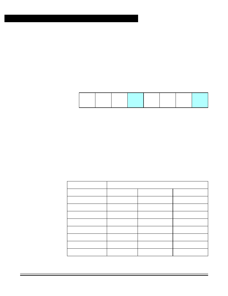
Technical Data
M68HC11K Family
236
Memory Expansion and Chip Selects
MOTOROLA
Memory Expansion and Chip Selects
11.3.2.3 Memory Mapping Window Base Register
The memory mapping window base register (MMWBR) defines the
starting address of each of the two windows within the CPU 64-Kbyte
address range. The windows normally begin at a boundary related to
their size (an 8-Kbyte window can begin on any 8-Kbyte boundary,
beginning at $0000).
W2A[15:13] -- Window 2 Base Address Bits
Selects the three most significant bits (MSB) of the base address for
memory mapping window 2. Refer to
Table 11-3
.
W1A[15:13] -- Window Base 1 Address Bits
Selects the three MSB of the base address for memory mapping
window 1. Refer to
Table 11-3
.
Address: $0057
Bit 7
6
5
4
3
2
1
Bit 0
Read:
W2A15
W2A14
W2A13
0
W1A15
W1A14
W1A13
0
Write:
Reset:
0
0
0
0
0
0
0
0
Figure 11-3. Memory Mapping Window Base Register (MMWBR)
Table 11-3. Memory Expansion Window Base Address
MSB Bits
Window Base Address
WxA[15:13]
8 Kbytes
16 Kbytes
32 Kbytes
000
$0000
$0000
$0000
001
$2000
$0000
$0000
010
$4000
$4000
$4000
011
$6000
$4000
$4000
100
$8000
$8000
$8000
101
$A000
$8000
$8000
110
$C000
$C000
$8000
111
$E000
$C000
$8000
Memory Expansion and Chip Selects
Memory Expansion
M68HC11K Family
Technical Data
MOTOROLA
Memory Expansion and Chip Selects
237
11.3.2.4 Memory Mapping Window Control Registers
Each of the memory mapping window control registers (MM1CR and
MM2CR) determine the active memory bank for the corresponding
window, containing the value to be output on the expansion address
lines when the CPU selects addresses within its extended memory
window. To change banks, write the address of the new bank into the
appropriate window register.
X1A[18:13] -- Memory Mapping Window 1 Expansion Address Line
Select Bits
X2A[18:13] -- Memory Mapping Window 2 Expansion Address Line
Select Bits
Each bit value written to the MMxCR registers is driven on the
corresponding port G expansion address line (if enabled by PGAR) to
enable the specified bank in the window.
Address: $0058
Memory Mapping Window 1 Control Register (MM1CR)
Bit 7
6
5
4
3
2
1
Bit 0
Read:
0
X1A18
X1A17
X1A16
X1A15
X1A14
X1A13
0
Write:
Reset:
0
0
0
0
0
0
0
0
Address: $0059
Memory Mapping Window 2 Control Register (MM1CR)
Read:
0
X2A18
X2A17
X2A16
X2A15
X2A14
X2A13
0
Write:
Reset:
0
0
0
0
0
0
0
0
Figure 11-4. Memory Mapping Window Control
Registers (MM1CR and MM2CR)

Technical Data
M68HC11K Family
238
Memory Expansion and Chip Selects
MOTOROLA
Memory Expansion and Chip Selects
11.4 Chip Selects
The M68HC11K Family microcontrollers contain a set of four
software-configured chip select signals which can reduce the amount of
external glue logic needed to interface the MCU to external devices in
the memory map. Each chip select signal is asserted when the CPU
accesses a memory location in its designated range, which is
determined by writes to control registers. Polarity of most chip-select
signals is programmable, as well as the segment of the address cycle
during which the signal is asserted (high E clock or address valid). Some
chip-select signals can be programmed to drive each other as well as
their own designated sections of memory (see
11.4.4 One Chip Select
Driving Another
), and the bus cycle during which any chip-select signal
is asserted can be "stretched" up to three clock cycles (see
11.4.5 Clock
Stretching
).
The four chip-select signals operate only in expanded modes. The
program chip select (CSPROG) is used to enable external memory in
the 64-Kbyte memory map that contains the reset vectors and program.
The chip select for I/O (CSIO) operates only within the first eight Kbytes
of the memory map. The two general-purpose chip selects, CSGP1 and
CSGP2, can enable devices anywhere in the 1-Mbyte expanded
memory space. Any port H pins 4-7 that are not used for chip-select
functions can serve as GPIO pins.
The six chip select control registers are:
�
CSCTL enables and controls most of the features in CSPROG
and CSIO.
�
GPCS1A, GPCS1C, GPCS2A, and GPCS2C define most of the
operations of the two general-purpose chip selects.
�
CSCSTR controls clock stretching for all four signals.
Table 11-4
summarizes the controls for each of the chip-select signals.
Memory Expansion and Chip Selects
Chip Selects
M68HC11K Family
Technical Data
MOTOROLA
Memory Expansion and Chip Selects
239
Table 11-4. Chip Select Control Parameter Summary
CSIO
Enable
IOEN in CSCTL
1 = enabled, 0 = disabled
(1)
Valid
IOCSA in CSCTL
1 = address valid, 0
(1)
= E high
Polarity
IOPL in CSCTL
1 = active high, 0 = active low
(1)
Size
IOSZ in CSCTL
1 = 4 K ($1000�$1FFF)
0 = 8 K ($0000�$1FFF)
(1)
Start address
Fixed (see size)
Stretch
IO1S[A:B] in CSCSTR
0
(1)
, 1, 2, or 3 E clocks
CSPROG
Enable
PCSEN in CSCTL
1 = enabled
(1)
, 0 = disabled
Valid
Fixed (address valid)
Polarity
Fixed (active low)
Size
PCSZ[A:B] in CSCTL
0:0 = 64 K ($0000�$FFFF)
(1)
0:1 = 32 K ($8000�$FFFF)
1:0 = 16 K ($C000�$FFFF)
1:1 = 8 K ($E000�$FFFF)
Start address
Fixed (see size)
Stretch
PCS[A:B] in CSCSTR
0
(1)
, 1, 2, or 3 E clocks
Priority
GCSPR in CSCTL
1 = CSGPx above CSPROG
0
(1)
= CSPROG above CSGPx
CSGP1,
Enable
Set size to 0K to disable
CSGP2
Valid
G1AV in GPCS1C
G2AV in GPCS2C
1 = address valid, 0 = E high
(1)
Polarity
G1POL in GPS1C
G2POL in GPS2C
1 = active high, 0 = active low
(1)
Size
G1SZ[A:D] in GPCS1C
G1SZ[A:D] in GPCS2C
2 K to 512 K in nine steps
0K = disabled
(1)
can also follow memory
expansion window 1 or window 2
Start address
GPCS1A
GPCS2A
Stretch
CSCSTR
0
(1)
, 1, 2, or 3 E clocks
Other
G1DG2 in GPCS1C
Allows CSGP1 and CSGP2 to be logically ORed
and driven out the CSGP2 pin
G1DPC in GPCS1C
Allows CSGP1 and CSPROG to be logically
ORed and driven out the CSPROG pin
G2DPC in GPCS2C
Allows CSGP2 and CSPROG to be logically
ORed and driven out the CSPROG pin.
MXGS2 in MMSIZ
Allows CSGP2 to follow either 64 K CPU
addresses or 512K expansion addresses
MXGS1 in MMSIZ
Allows CSGP1 to follow either 64 K CPU
addresses or 512K expansion addresses
1. Configuration at reset
Technical Data
M68HC11K Family
240
Memory Expansion and Chip Selects
MOTOROLA
Memory Expansion and Chip Selects
11.4.1 Program Chip Select
The program chip select signal accesses external memory in the main
program area within the MCU's 64-Kbyte memory map. Program chip
select validity is fixed at address valid timing and polarity is fixed at active
low. The chip-select control register (CSCTL) contains bits to enable
CSPROG, determine its priority over the general-purpose chip selects,
and set its effective address range. Clock stretching can be set from zero
to three cycles.
GCSPR -- General-Purpose Chip Select Priority Bit
0 = Program chip select has priority over general-purpose chip
selects
1 = General-purpose chip selects have priority over program chip
select
PCSEN -- Program Chip Select Enable Bit
0 = CSPROG disabled and port H bit 7 available as GPIO
1 = CSPROG enabled out of reset and uses port H bit 7 pin
PCSZA and PCSZB -- Program Chip Select Size A Bit and Program
Chip Select Size B Bit
These bits determine the address range of CSPROG, as shown in
Table 11-5
.
Address: $005B
Bit 7
6
5
4
3
2
1
Bit 0
Read:
IOEN
IOPL
IOCSA
IOSZ
GCSPR
PCSEN
PCSZA
PCSZB
Write:
Reset:
0
0
0
0
0
1
0
0
Figure 11-5. Chip-Select Control Register (CSCTL)
Table 11-5. Program Chip Select Size
PCSZA
PCSZB
Size (Bytes)
Address Range
0
0
64 K
$0000�$FFFF
0
1
32 K
$8000�$FFFF
1
0
16 K
$C000�$FFFF
1
1
8 K
$E000�$FFFF

Memory Expansion and Chip Selects
Chip Selects
M68HC11K Family
Technical Data
MOTOROLA
Memory Expansion and Chip Selects
241
11.4.2 Input/Output Chip Select
The I/O chip select (CSIO) is programmable for a 4-Kbyte size located
at addresses $1000�$1FFF or 8-Kbyte size located at addresses
$0000�$1FFF. The default active-low polarity can be changed to active
high by setting the IOPL bit in CSCTL. Default validity during high E clock
can be changed to address valid time by setting the IOCSA bit in CSCTL.
Clock stretching can be set from zero to three cycles (See
11.4.5 Clock
Stretching
). CSIO is disabled out of reset.
IOEN -- I/O Chip-Select Enable Bit
0 = CSIO is disabled and port H bit 4 is GPIO.
1 = CSIO is enabled and uses port H bit 4.
IOPL -- I/O Chip-Select Polarity Select Bit
0 = CSIO active low
1 = CSIO active high
IOCSA -- I/O Chip-Select Address Valid Bit
0 = CSIO is valid during E-clock high time.
1 = CSIO is valid during address valid time.
IOSZ -- I/O Chip-Select Size Select Bit
0 = CSIO size is four Kbytes at $1000�$1FFF.
1 = CSIO size is eight Kbytes at $0000�$1FFF.
Address: $005B
Bit 7
6
5
4
3
2
1
Bit 0
Read:
IOEN
IOPL
IOCSA
IOSZ
GCSPR
PCSEN
PCSZA
PCSZB
Write:
Reset:
0
0
0
0
0
1
0
0
Figure 11-6. Chip-Select Control Register (CSCTL)

Technical Data
M68HC11K Family
242
Memory Expansion and Chip Selects
MOTOROLA
Memory Expansion and Chip Selects
11.4.3 General-Purpose Chip Selects
The general-purpose chip selects are the most flexible and
programmable of the chip-select signals. They can access any memory
in the expanded 1-Mbyte address space. Polarity of active state, E valid
or address valid, size, and starting address are all programmable. Clock
stretching can be set from zero to three cycles. Both signals can be
programmed to drive CSPROG, and GPCS1 can be configured to drive
GPCS2. In addition, each signal can follow a window; for instance, be
asserted whenever the CPU address falls within a selected memory
expansion window regardless of the state of the expanded address
lines.
There are two registers for each of the general-purpose chip select
signals:
�
The control register, GPS1C or GPS2C, determines the GPCS's
active signal polarity, its valid time, which of the other chip-select
signals it can drive, and either the size of the memory it enables or
which window it follows.
�
The address register, GPS1A or GPS2A, programs the
chip-select's starting address; valid bits in this register are
determined by the size of the address range selected by the
control register.
In addition, the MMSIZ register contains a bit for each GPCS which
determines whether it is driven by the CPU's 64-Kbyte address lines or
the expansion address lines.

Memory Expansion and Chip Selects
Chip Selects
M68HC11K Family
Technical Data
MOTOROLA
Memory Expansion and Chip Selects
243
11.4.3.1 Memory Mapping Size Register
MXGS2 -- Memory Expansion Select for GPCS 2 Bit
0 = GPCS 2 based on 64-Kbyte CPU address
1 = GPCS 2 based on expansion address
MXGS1 -- Memory Expansion Select for GPCS 1 Bit
0 = GPCS 1 based on 64-Kbyte CPU address
1 = GPCS 1 based on expansion address
11.4.3.2 General-Purpose Chip Select 1 Address Register
G1A[18:11] -- General-Purpose Chip Select 1 Address Bits
They select the starting address of GPCS1. Refer to
Table 11-6
.
Address: $0056
Bit 7
6
5
4
3
2
1
Bit 0
Read:
MXGS2
MXGS1
W2SZ1
W2SZ0
0
0
W1SZ1
W1SZ0
Write:
Reset:
0
0
0
0
0
0
0
0
Figure 11-7. Memory Mapping Size Register (MMSIZ)
Address: $005C
Bit 7
6
5
4
3
2
1
Bit 0
Read:
G1A18
G1A17
G1A16
G1A15
G1A14
G1A13
G1A12
G1A11
Write:
Reset:
0
0
0
0
0
0
0
0
Figure 11-8. General-Purpose Chip Select 1
Address Register (GPCS1A)
Technical Data
M68HC11K Family
244
Memory Expansion and Chip Selects
MOTOROLA
Memory Expansion and Chip Selects
11.4.3.3 General-Purpose Chip Select 1 Control Register
G1POL -- General-Purpose Chip Select 1 Polarity Select Bit
0 = CSGP1 active low
1 = CSGP1 active high
G1AV -- General-Purpose Chip Select 1 Address Valid Select Bit
0 = CSGP1 is valid during E high time.
1 = CSGP1 is valid during address valid time.
G1SZ[A:D] -- General-Purpose Chip Select 1 Size Bits
They select the range of GPCS1. Refer to
Table 11-6
.
Address: $005D
Bit 7
6
5
4
3
2
1
Bit 0
Read:
G1DG2
G1DPC
G1POL
G1AV
G1SZA
G1SZB
G1SCC
G1SZD
Write:
Reset:
0
0
0
0
0
0
0
0
Figure 11-9. General-Purpose Chip Select 1
Control Register (GPCS1C)
Table 11-6. General-Purpose Chip Select 1 Size Control
G1SZ[A:D]
Size (Bytes)
Valid Bits
(MXGS1 = 0)
Valid Bits
(MXGS1 = 1)
0 0 0 0
Disabled
None
None
0 0 0 1
2 K
G1A[15:11]
G1A[18:11]
0 0 1 0
4 K
G1A[15:11]
G1A[18:12]
0 0 1 1
8 K
G1A[15:13]
G1A[18:13]
0 1 0 0
16 K
G1A[15:14]
G1A[18:14]
0 1 0 1
32 K
G1A[15]
G1A[18:15]
0 1 1 0
64 K
None
G1A[18:16]
0 1 1 1
128 K
None
G1A[18:17]
1 0 0 0
256 K
None
G1A18
1 0 0 1
512 K
None
None
1 0 1 0
Follow window 1
None
None
1 0 1 1
Follow window 2
None
None
1100�1111
Default to 512 K
None
None

Memory Expansion and Chip Selects
Chip Selects
M68HC11K Family
Technical Data
MOTOROLA
Memory Expansion and Chip Selects
245
11.4.3.4 General-Purpose Chip Select 2 Address Register
G2A[18:11] -- General-Purpose Chip Select 2 Address Bits
They select the starting address of GPCS2. Refer to
Table 11-7
.
11.4.3.5 General-Purpose Chip Select 2 Control Register
G2POL -- General-Purpose Chip Select 2 Polarity Select Bit
0 = CSGP2 active low
1 = CSGP2 active high
G2AV -- General-Purpose Chip Select 2 Address Valid Select Bit
0 = CSGP2 is valid during E high time.
1 = CSGP2 is valid during address valid time.
G2SZ[A:D] -- General-Purpose Chip Select 2 Size Bits
They select the range of GPCS2. Refer to
Table 11-7
.
Address: $005E
Bit 7
6
5
4
3
2
1
Bit 0
Read:
G2A18
G2A17
G2A16
G2A15
G2A14
G2A13
G2A12
G2A11
Write:
Reset:
0
0
0
0
0
0
0
0
Figure 11-10. General-Purpose Chip Select 2
Address Register (GPCS2A)
Address: $005F
Bit 7
6
5
4
3
2
1
Bit 0
Read:
0
G2DPC
G2POL
G2AV
G2SZA
G2SZB
G2SZC
G2SZD
Write:
Reset:
0
0
0
0
0
0
0
0
Figure 11-11. General-Purpose Chip Select 2
Control Register (GPCS2C)
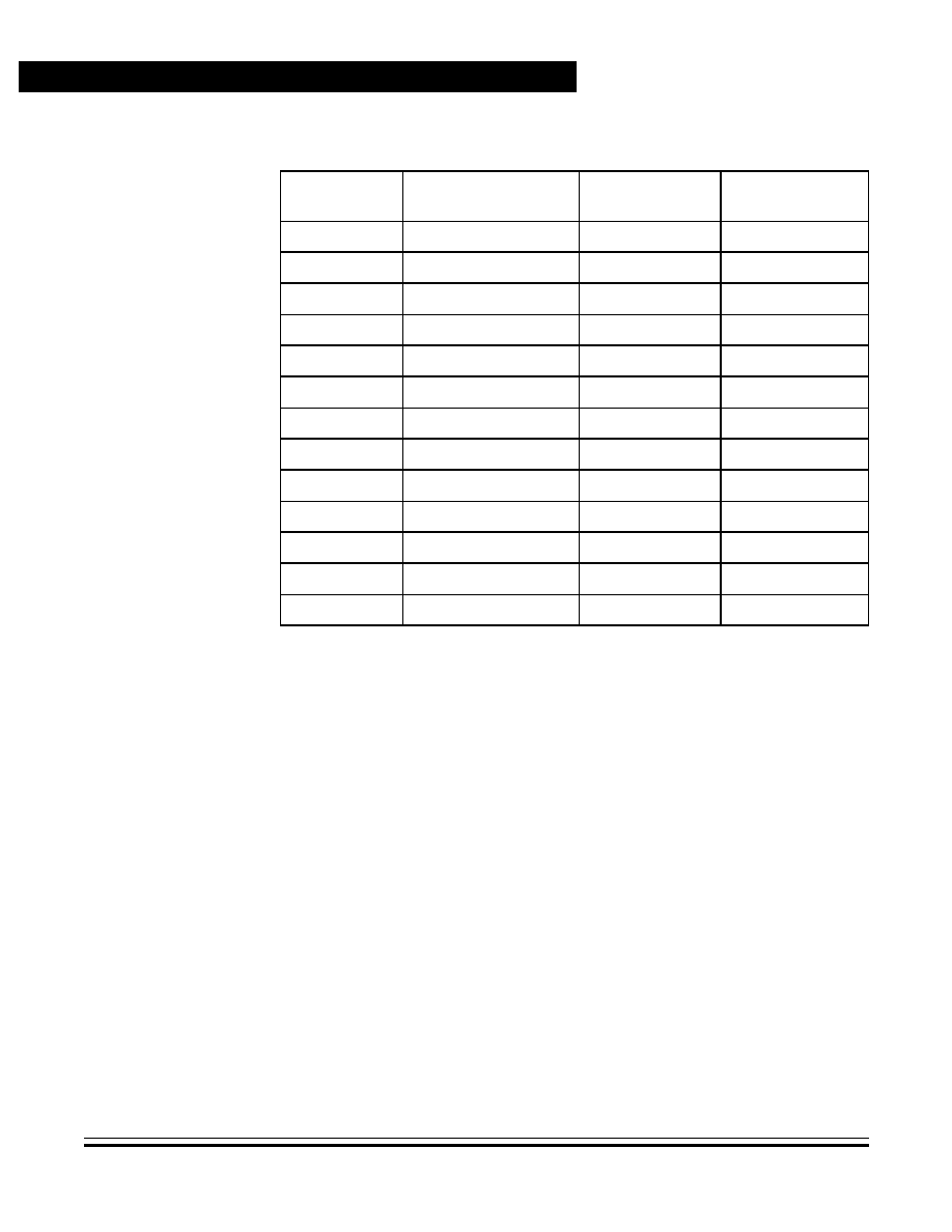
Technical Data
M68HC11K Family
246
Memory Expansion and Chip Selects
MOTOROLA
Memory Expansion and Chip Selects
11.4.4 One Chip Select Driving Another
The general-purpose chip selects can be programmed to drive other
chip-select signals as well as their own memory areas. Although all of
the eight possible combinations of the bits G1DG2, G1DPC, and G2DPC
are allowed, some combinations cause operations which do not
perform as one might expect. The results of all combinations are defined
in
Table 11-8
. The priorities defined in the previous sections still apply.
The table assumes that none of the chip-select ranges overlap.
Table 11-7. General-Purpose Chip Select 2 Size Control
G2SZ[A:D]
Size
(Bytes)
Valid Bits
(MXGS2 = 0)
Valid Bits
(MXGS2 = 1)
0 0 0 0
Disabled
None
None
0 0 0 1
2 K
G2A[15:11]
G2A[18:11]
0 0 1 0
4 K
G2A[15:11]
G2A[18:12]
0 0 1 1
8 K
G2A[15:13]
G2A[18:13]
0 1 0 0
16 K
G2A[15:14]
G2A[18:14]
0 1 0 1
32 K
G2A[15]
G2A[18:15]
0 1 1 0
64 K
None
G2A[18:16]
0 1 1 1
128 K
None
G2A[18:17]
1 0 0 0
256 K
None
G2A18
1 0 0 1
512 K
None
None
1 0 1 0
Follow window 1
None
None
1 0 1 1
Follow window 2
None
None
1100�1111
Default to 512 K
None
None
Memory Expansion and Chip Selects
Chip Selects
M68HC11K Family
Technical Data
MOTOROLA
Memory Expansion and Chip Selects
247
11.4.4.1 General-Purpose Chip Select 1 Control Register
G1DG2 -- GPCS 1 Drives GPCS 2 Bit
0 = CSGP1 does not affect CSGP2.
1 = CSGP1 and CSGP2 are ORed and driven out of the CSGP2.
G1DPC -- General-Purpose Chip Select 1 Drives Program Chip
Select Bit
0 = CSGP1 does not affect CSPROG.
1 = CSGP1 and CSPROG are ORed and driven out of the
CSPROG.
11.4.4.2 General-Purpose Chip Select 2 Control Register
G2DPC -- General-Purpose Chip Select 2 Drives Program Chip
Select Bit
0 = Does not affect program chip select
1 = CSGP2 and CSPROG are ORed and driven out of the
CSPROG pin.
Address: $005D
Bit 7
6
5
4
3
2
1
Bit 0
Read:
G1DG2
G1DPC
G1POL
G1AV
G1SZA
G1SZB
G1SCC
G1SZD
Write:
Reset:
0
0
0
0
0
0
0
0
Figure 11-12. General-Purpose Chip Select 1
Control Register (GPCS1C)
Address: $005F
Bit 7
6
5
4
3
2
1
Bit 0
Read:
0
G2DPC
G2POL
G2AV
G2SZA
G2SZB
G2SZC
G2SZD
Write:
Reset:
0
0
0
0
0
0
0
0
Figure 11-13. General-Purpose Chip Select 2
Control Register (GPCS2C)
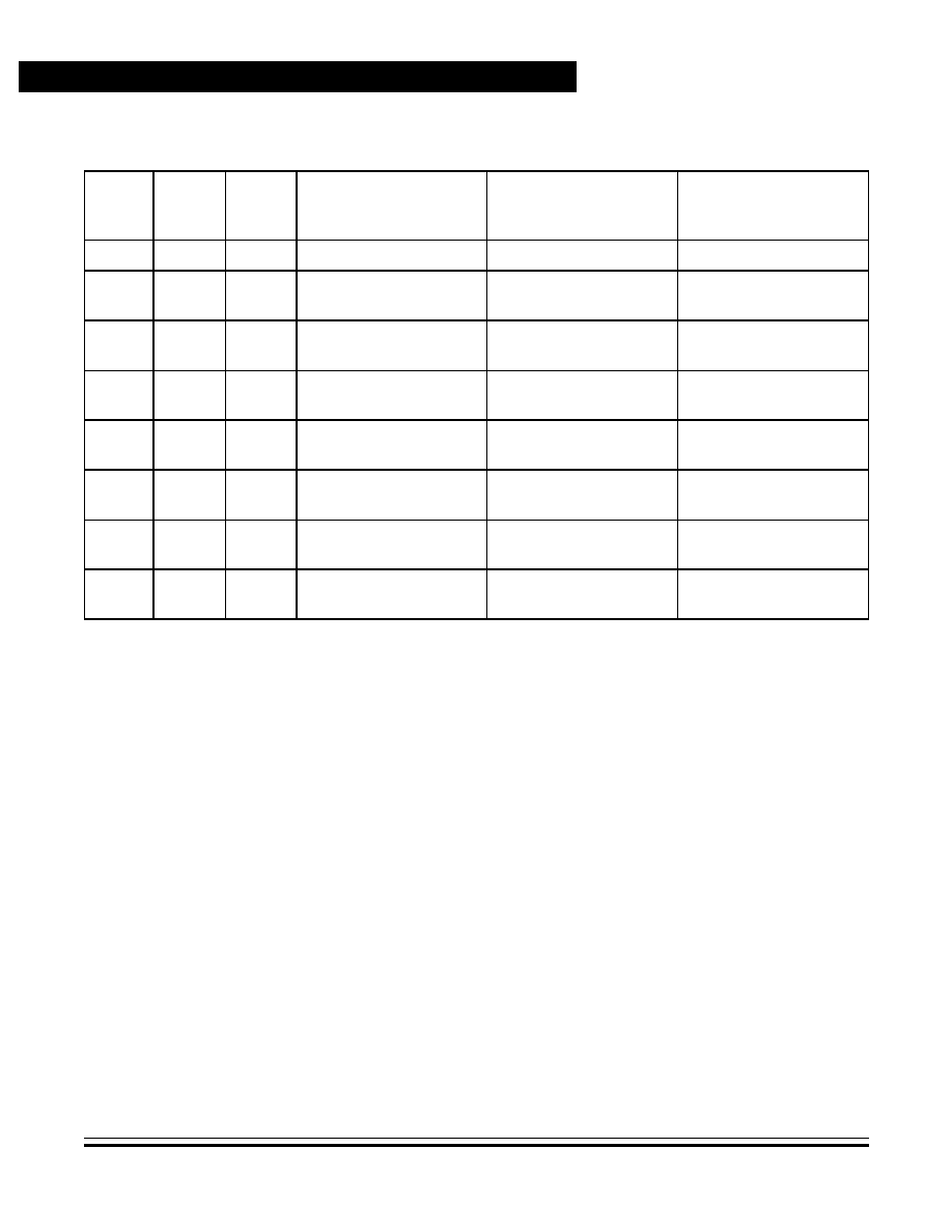
Technical Data
M68HC11K Family
248
Memory Expansion and Chip Selects
MOTOROLA
Memory Expansion and Chip Selects
11.4.5 Clock Stretching
Chip select and bus control signals are synchronized with the external
E clock. To accommodate devices that are slower than the MCU, the
E clock can be stretched when a chip select is asserted so that it remains
high for one to three extra bus cycles. During this stretch, which can
occur only during accesses to addresses in that chip select's address
range, the other clocks continue running normally, maintaining the
integrity of the timers and baud generators. Each chip select has two
associated bits in the chip-select clock stretch (CSCSTR) register that
set its clock stretching from zero (disabled) to three cycles.
Table 11-8. One Chip Select Driving Another
G1DG2
G1DPC
G2DPC
Program CS Pin
is Asserted
When Address is in:
General 2 CS Pin
is Asserted
When Address is in:
General 1 CS Pin
is Asserted
When Address is in:
0
0
0
A valid program area
A valid general 2 area
A valid general 1 area
0
0
1
A valid program
or general 2 area
Never asserted
A valid general 1 area
0
1
0
A valid program
or general 1 area
A valid general 2 area
Never asserted
0
1
1
A valid program
or general 1 or 2 area
Never asserted
Never asserted
1
0
0
A valid program area
A valid general 2
or general 1 area
Never asserted
1
0
1
A valid program
or general 2 area
Never asserted
A valid general 1 area
1
1
0
A valid program
or general 1 area
A valid general 2 area
Never asserted
1
1
1
A valid program
or general 1 or 2 area
Never asserted
Never asserted
Memory Expansion and Chip Selects
Memory Expansion Examples
M68HC11K Family
Technical Data
MOTOROLA
Memory Expansion and Chip Selects
249
IOS[A:B] -- CSIO Stretch Select Bits
GP1S[A:B] -- CSGP1 Stretch Select Bits
GP2S[A:B] -- CSGP2 Stretch Select Bits
PCS[A:B] -- CSPROG Stretch Select Bits
Each of these pairs of bits contain the binary number of cycles of clock
stretch, as shown in
Table 11-9
.
11.5 Memory Expansion Examples
The first example, shown in
Figure 11-15
contains a system with
64 Kbytes of external memory to be accessed through a single 8-Kbyte
window. To access eight Kbytes, or 2
13
address locations, the CPU will
need 13 address lines, ADDR[12:0]. The number of memory banks
needed is the total memory, 64 Kbytes divided by the window size, eight
Kbytes. This yields eight memory banks, or 2
3
. Thus, three expansion
lines are required, so expansion address lines XA[15:13] replace CPU
address lines ADDR[15:13].
Figure 1-1
shows a memory map and
schematic drawing of this system.
Address: $005A
Bit 7
6
5
4
3
2
1
Bit 0
Read:
IOSA
IOSB
GP1SA
GP1SB
GP2SA
GP2SB
PCSA
PCSB
Write:
Reset:
0
0
0
0
0
0
0
0
Figure 11-14. Chip Select Clock Stretch Register (CSCSTR)
Table 11-9. CSCSTR Bits Versus Clock Cycles
Bit [A:B]
Clock Stretch
0 0
None
0 1
1 cycle
1 0
2 cycles
1 1
3 cycles

Technical Data
M68HC11K Family
250
Memory Expansion and Chip Selects
MOTOROLA
Memory Expansion and Chip Selects
Figure 11-15. Memory Expansion Example 1 -- Memory Map for a Single
8-Kbyte Window with Eight Banks of External Memory
INTERNAL
(EP)ROM
$04000
BANK 0
XA[15:13] =
0:0:0
$0000
$1000
$4000
$6000
$A000
$FFFF
WINDOW 1
CHIP SELECT 1
PGAR = $07
XA[15:13]
MMWBR = $04
Window 1 @ $4000
Window 2 disabled
MMSIZ = $41
Window 1 = 8 Kbytes
Window 2 disabled
General-purpose chip select 1 based on
expanded address
CSCTL = $00
No I/O or program chip selects
GPCS1A = $00
General-purpose chip select 1 starting address = $00000
GPCS1C = $06
64 Kbyte range (8 x 8 K)
GPCS2A = $00
N/A
GPCS2C = $00
General-purpose chip select 2 disabled
27C512
MC68HC(7)11K
GPCS2
GPCS1
E
R/W
$05FFF
$14000
BANK 1
XA[15:13] =
0:0:1
$15FFF
$24000
BANK2
XA[15:13] =
0:1:0
$25FFF
$34000
BANK 3
XA[15:13] =
0:1:1
$35FFF
$44000
BANK 4
XA[15:13] =
1:0:0
$45FFF
$54000
BANK 5
XA[15:13] =
1:0:1
$55FFF
$64000
BANK6
XA[15:13] =
1:1:0
$65FFF
$74000
BANK 7
XA[15:13] =
1:1:1
$75FFF
EE/REG/RAM
ADDR7
ADDR6
ADDR5
ADDR4
ADDR3
ADDR2
ADDR1
ADDR0
ADDR7
ADDR6
ADDR5
ADDR4
ADDR3
ADDR2
ADDR1
ADDR0
ADDR11
ADDR10
ADDR9
ADDR8
ADDR11
ADDR10
ADDR9
ADDR8
ADDR15
ADDR14
ADDR13
ADDR12
ADDR12
DATA7
DATA6
DATA5
DATA4
DATA3
DATA2
DATA1
DATA0
DATA7
DATA6
DATA5
DATA4
DATA3
DATA2
DATA1
DATA0
ADDR7
ADDR6
ADDR5
ADDR4
ADDR3
ADDR2
ADDR1
ADDR0
A7
A6
A5
A4
A3
A2
A1
A0
ADDR8
A8
ADDR11
ADDR10
ADDR9
A11
A10
A9
A12
ADDR12
XA15
XA14
XA13
A15
A14
A13
V
SS
OE
CE
V
CC
V
DD
XA13
XA13
XA15
XA14
XA17
XA16
XA15
XA14
XA18
DATA7
DATA6
DATA5
DATA4
DATA3
DATA2
DATA1
DATA0
D7
D6
D5
D4
D3
D2
D1
D0
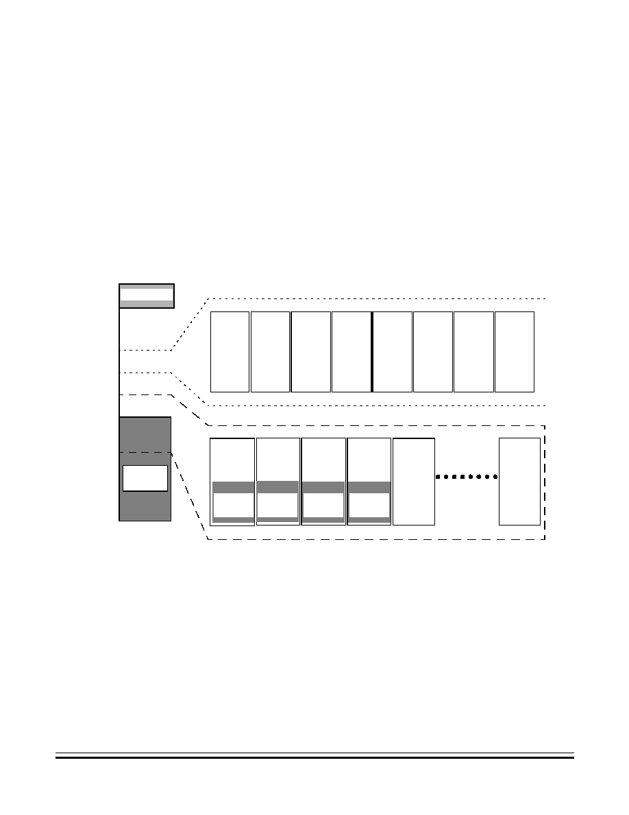
Memory Expansion and Chip Selects
Memory Expansion Examples
M68HC11K Family
Technical Data
MOTOROLA
Memory Expansion and Chip Selects
251
The second example system shown in
Figure 11-16
contains two
memory windows. The first window is organized as in the previous
example, 8 banks of 8 Kbytes each. The second window accesses
256 Kbytes of memory in 16 banks of 16 Kbyte each. To access
16 Kbytes, or 2
14
address locations, the CPU will need 14 address lines,
ADDR[13:0]. Since ADDR13 is driven on XA13 in this example, XA13
replaces ADDR13 to drive the A13 line in the 6226 devices, but ADDR13
could be used as well. 16 (2
4
) memory banks require four expansion
address lines, A[17:14]. Refer to
Figure 11-16
for a memory map and
schematic drawing of this system.
Figure 11-16. Memory Expansion Example 2 (Sheet 1 of 2)
Memory Map for One 8-Kbyte Window with Eight Banks and
One 16-Kbyte Window with 16 Banks of External Memory
XA[17:14] =
0:0:0:0
INTERNAL
(EP)ROM
$0000
$1000
$4000
$6000
$A000
$FFFF
WINDOW 1
CHIP
EE/REG/RAM
WINDOW 2
$08000
BANK 0
$0BFFF
$18000
BANK 1
$1BFFF
$28000
BANK 2
$2BFFF
$38000
BANK 3
$3BFFF
$48000
BANK 4
XA[17:14] =
0:1:0:0
$4BFFF
$F8000
BANK 15
XA[17:14] =
1:1:1:1
$FBFFF
SELECT
1
CHIP
SELECT
2
$8000
$C000
PGAR = $1F
XA[17:13]
CSCTL
= $00
No I/O or program chip selects
MMWBR = $84
Window 1 @ $4000
GPCS1A
= $00
General-purpose chip select 1 from $00000
Window 2 @ $8000
GPCS1C
= $06
64 KByte range (8 x 8 K)
MMSIZ = $E1
Window 1 = 8 Kbytes
GPCS2A
= $00
General-purpose chip select 2 from $00000
Window 2 = 16 Kbytes
GPCS2C
= $08
256 KByte range (16 x 16 K)
GPCS1, GPCS2 based
on expansion address
$04000
BANK 0
XA[15:13] =
0:0:0
$05FFF
$14000
BANK 1
XA[15:13] =
0:0:1
$15FFF
$24000
BANK2
XA[15:13] =
0:1:0
$25FFF
$34000
BANK 3
XA[15:13] =
0:1:1
$35FFF
$44000
BANK 4
XA[15:13] =
1:0:0
$45FFF
$54000
BANK 5
XA[15:13] =
1:0:1
$55FFF
$64000
BANK6
XA[15:13] =
1:1:0
$65FFF
$74000
BANK 7
XA[15:13] =
1:1:1
$75FFF
XA[17:14] =
0:0:0:1
XA[17:14] =
0:0:1:0
XA[17:14] =
0:0:1:1
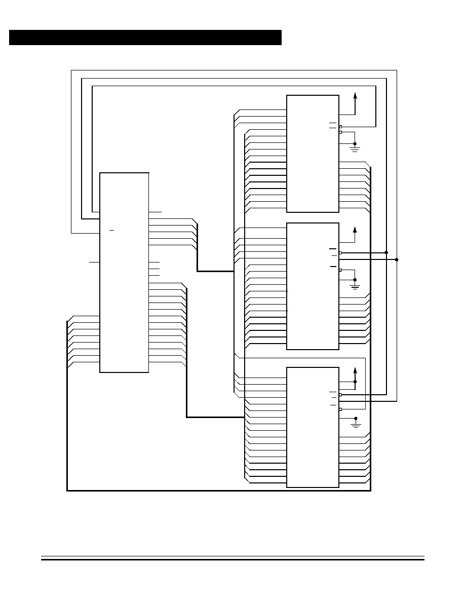
Technical Data
M68HC11K Family
252
Memory Expansion and Chip Selects
MOTOROLA
Memory Expansion and Chip Selects
Figure 11-16. Memory Expansion Example 2 (Sheet 2 of 2)
Memory Map for One 8-Kbyte Window with Eight Banks and
One 16-Kbyte Window with 16 Banks of External Memory
MC68HC(7)11K
6226
ADDR7
ADDR6
ADDR5
ADDR4
ADDR3
ADDR2
ADDR1
ADDR0
ADDR7
ADDR6
ADDR5
ADDR4
ADDR3
ADDR2
ADDR1
ADDR0
ADDR11
ADDR10
ADDR9
ADDR8
ADDR11
ADDR10
ADDR9
ADDR8
DATA7
DATA6
DATA5
DATA4
DATA3
DATA2
DATA1
DATA0
DATA7
DATA6
DATA5
DATA4
DATA3
DATA2
DATA1
DATA0
XA13
XA13
XA17
XA16
XA15
XA14
XA17
XA16
XA15
XA14
ADDR15
ADDR14
ADDR13
ADDR12
XA18
ADDR12
ADDR7
ADDR6
ADDR5
ADDR4
ADDR3
ADDR2
ADDR1
ADDR0
A7
A6
A5
A4
A3
A2
A1
A0
ADDR8
A8
ADDR11
ADDR10
ADDR9
A11
A10
A9
A12
ADDR12
XA15
XA14
XA13
A15
A14
A13
XA16
A16
(LOW)
DATA7
DATA6
DATA5
DATA4
DATA3
DATA2
DATA1
DATA0
D7
D6
D5
D4
D3
D2
D1
D0
V
SS
OE
E1
V
CC
V
DD
W
E2
6226
ADDR7
ADDR6
ADDR5
ADDR4
ADDR3
ADDR2
ADDR1
ADDR0
A7
A6
A5
A4
A3
A2
A1
A0
ADDR8
A8
ADDR11
ADDR10
ADDR9
A11
A10
A9
A12
ADDR12
XA15
XA14
XA13
A15
A14
A13
XA16
A16
(HIGH)
DATA7
DATA6
DATA5
DATA4
DATA3
DATA2
DATA1
DATA0
D7
D6
D5
D4
D3
D2
D1
D0
V
SS
OE
E1
V
CC
V
DD
W
27C512
DATA7
DATA6
DATA5
DATA4
DATA3
DATA2
DATA1
DATA0
D7
D6
D5
D4
D3
D2
D1
D0
V
SS
OE
CE
V
CC
V
DD
R/W
GPCS2
GPCS1
ADDR7
ADDR6
ADDR5
ADDR4
ADDR3
ADDR2
ADDR1
ADDR0
A7
A6
A5
A4
A3
A2
A1
A0
ADDR8
A8
ADDR11
ADDR10
ADDR9
A11
A10
A9
A12
ADDR12
XA15
XA14
XA13
A15
A14
A13
E
XA17
XA17
E2

M68HC11K Family
Technical Data
MOTOROLA
Electrical Characteristics
253
Technical Data -- M68HC11K Family
Section 12. Electrical Characteristics
12.1 Contents
12.2
Introduction . . . . . . . . . . . . . . . . . . . . . . . . . . . . . . . . . . . . . . . 254
12.3
Maximum Ratings for Standard Devices . . . . . . . . . . . . . . . . 254
12.4
Functional Operating Range. . . . . . . . . . . . . . . . . . . . . . . . . . 255
12.5
Thermal Characteristics . . . . . . . . . . . . . . . . . . . . . . . . . . . . . 255
12.6
Electrical Characteristics . . . . . . . . . . . . . . . . . . . . . . . . . . . . 256
12.7
Power Dissipation Characteristics . . . . . . . . . . . . . . . . . . . . . 257
12.8
Control Timing . . . . . . . . . . . . . . . . . . . . . . . . . . . . . . . . . . . . 259
12.9
Peripheral Port Timing . . . . . . . . . . . . . . . . . . . . . . . . . . . . . . 263
12.10 Analog-to-Digital Converter Characteristics . . . . . . . . . . . . . . 265
12.11 Expansion Bus Timing . . . . . . . . . . . . . . . . . . . . . . . . . . . . . . 267
12.12 Serial Peripheral Interface Timing . . . . . . . . . . . . . . . . . . . . . 269
12.13 EEPROM Characteristics . . . . . . . . . . . . . . . . . . . . . . . . . . . .272
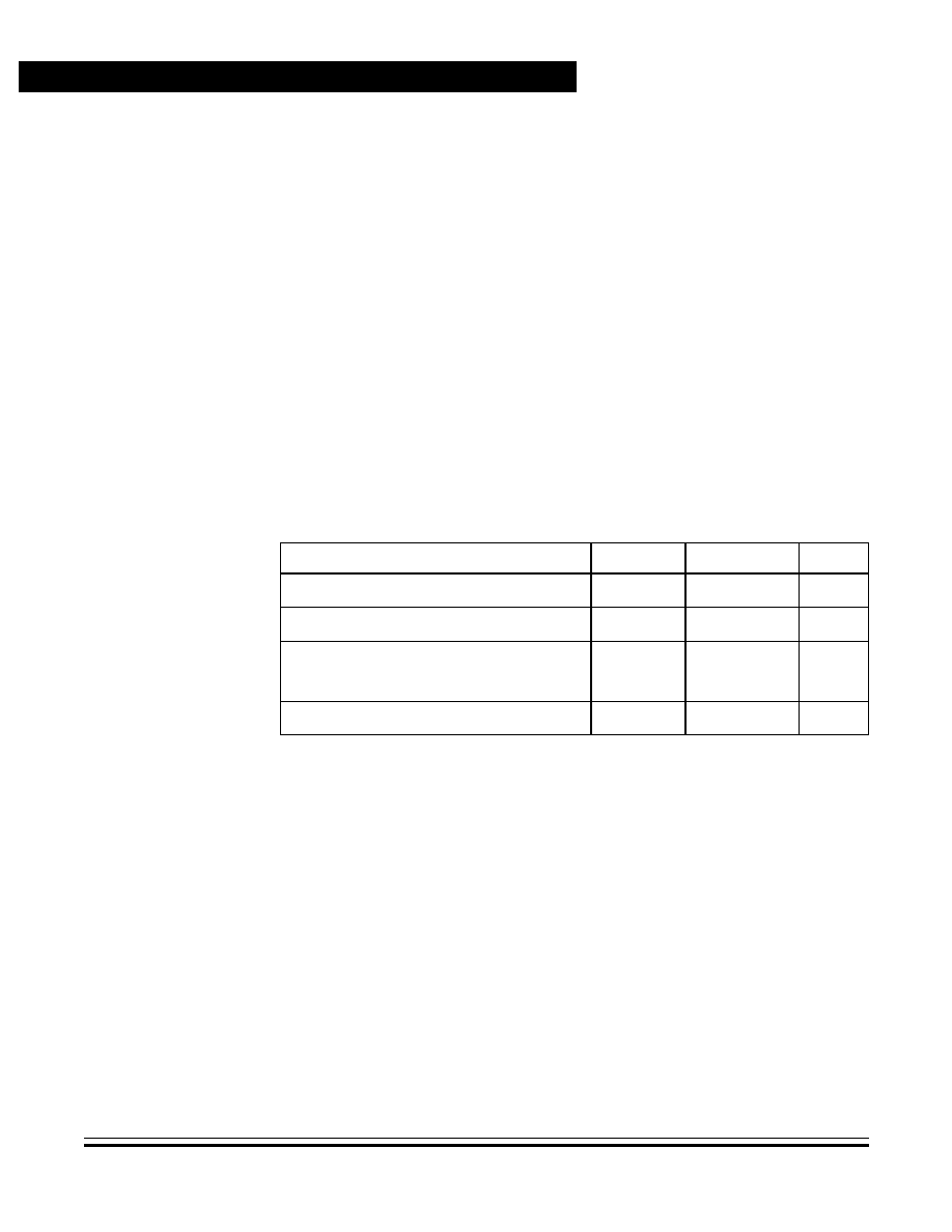
Technical Data
M68HC11K Family
254
Electrical Characteristics
MOTOROLA
Electrical Characteristics
12.2 Introduction
This section contains electrical parameters for standard and extended
voltage devices. When applicable, extended voltage parameters are
shown separately. Diagrams apply to both standard and extended
voltage devices.
12.3 Maximum Ratings for Standard Devices
Maximum ratings are the extreme limits to which the MCU can be
exposed without permanently damaging it.
NOTE:
This device is not guaranteed to operate properly at the maximum
ratings. Refer to
12.6 Electrical Characteristics
for guaranteed
operating conditions.
NOTE:
This device contains circuitry to protect the inputs against damage due
to high static voltages or electric fields; however, it is advised that normal
precautions be taken to avoid application of any voltage higher than
maximum-rated voltages to this high-impedance circuit. For proper
operation, it is recommended that V
In
and V
Out
be constrained to the
range V
SS
(V
In
or V
Out
)
V
DD
. Reliability of operation is enhanced if
unused inputs are connected to an appropriate logic voltage level (for
example, either V
SS
or V
DD
).
Rating
Symbol
Value
Unit
Supply voltage
V
DD
�0.3 to +7.0
V
Input voltage
V
In
�0.3 to +7.0
V
Current drain per pin
(1)
excluding V
DD
,
V
SS
, AV
DD
, V
RH
, and V
RL
1. One pin at a time, observing maximum power dissipation limits
I
D
25
mA
Storage temperature
T
STG
�55 to +150
�
C
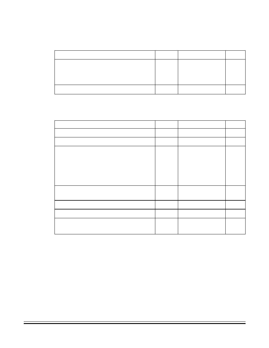
Electrical Characteristics
Functional Operating Range
M68HC11K Family
Technical Data
MOTOROLA
Electrical Characteristics
255
12.4 Functional Operating Range
12.5 Thermal Characteristics
Rating
Symbol
Value
Unit
Operating temperature range
MC68HC(7)11KC
MC68HC(7)11KV
MC68HC(7)11KM
T
A
T
L
to T
H
-
40 to
+
85
-
40 to
+
105
-
40 to
+
125
�
C
Operating voltage range
V
DD
5.0
�
10%
V
Characteristic
Symbol
Value
Unit
Average junction temperature
T
J
T
A
+
(P
D
�
JA
)
�
C
Ambient temperature
T
A
User-determined
�
C
Package thermal resistance (junction-to-ambient)
80-pin low-profile quad flat pack
68-pin plastic leaded chip carrier
68-pin windowed ceramic cerquad (EPROM)
84-pin plastic leaded chip carrier
80-pin quad flat pack
84-pin J-cerquad
JA
80
50
60
50
85
50
�
C/W
Total power dissipation
(1)
1. This is an approximate value, neglecting P
I/O
.
P
D
P
INT
+
P
I/O
K / T
J
+
273
�
C
W
Device internal power dissipation
P
INT
I
DD
�
V
DD
W
I/O pin power dissipation
(2)
2. For most applications, P
I/O
P
INT
and can be neglected.
P
I/O
User-determined
W
A constant
(3)
3. K is a constant pertaining to the device. Solve for K with a known T
A
and a measured P
D
(at equilibrium).
Use this value of K to solve for P
D
and T
J
iteratively for any value of T
A
.
K
P
D
�
(T
A
+
273
�
C)
+
JA
�
P
D
2
W/
�
C
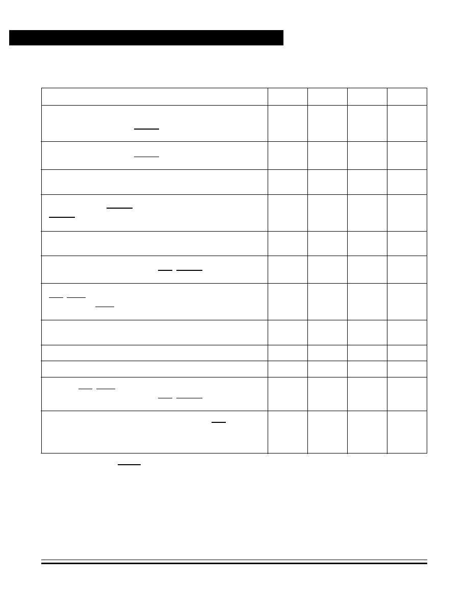
Technical Data
M68HC11K Family
256
Electrical Characteristics
MOTOROLA
Electrical Characteristics
12.6 Electrical Characteristics
Characteristic
(1)
1. V
DD
= 5.0 Vdc
�
10%, V
SS
= 0 Vdc, T
A
= T
L
to T
H
, unless otherwise noted
Symbol Min
Max
Unit
Output voltage, I
Load
=
�
10.0
�
A
(2)
)
All outputs except XTAL
All outputs except XTAL, RESET, and MODA
2. V
OH
specification for RESET and MODA is not applicable because they are open-drain pins. V
OH
specification not
applicable to ports C and D in wired-OR mode.
V
OL
V
OH
--
V
DD
� 0.1
0.1
--
V
Output high voltage, I
Load
= � 0.8 mA, V
DD
= 4.5 V
(2)
All outputs except XTAL, RESET, and MODA
V
OH
V
DD
� 0.8
--
V
Output low voltage, I
Load
= 1.6 mA
All outputs except XTAL
V
OL
-- 0.4
V
Input high voltage
All inputs except RESET
RESET
V
IH
0.7 x V
DD
0.8 x V
DD
V
DD
+ 0.3
V
DD
+ 0.3
V
Input low voltage
All Inputs
V
IL
V
SS
� 0.3
0.2 x V
DD
V
I/O ports, three-state leakage, V
In
= V
IH
or V
IL
Ports A, B, C, D, F, G, H, MODA/LIR, RESET
I
OZ
--
�
10
�
A
Input leakage current, V
In
= V
DD
or V
SS
(3)
IRQ, XIRQ on standard devices
MODB/V
STBY
, XIRQ on EPROM devices
3. Refer to
12.10 Analog-to-Digital Converter Characteristics
for leakage current for port E.
I
I
n
--
--
�
1
�
10
�
A
Input current with pullup resistors, V
In
= V
IL
Ports B, F, G, and H
l
IPR
100
500
�
A
RAM standby voltage, power down
V
SB
2.0
V
DD
V
RAM standby current, power down
I
SB
-- 10
�
A
Input capacitance
PE[7:0], IRQ, XIRQ, EXTAL
Ports A, B, C, D, F, G, H, MODA/LIR, RESET
C
In
--
--
8
12
pF
Output load capacitance
All outputs except PD[4:1], XOUT, XTAL, MODA/LIR
PD[4:1]
XOUT
C
L
--
--
--
90
200
30
pF

Electrical Characteristics
Power Dissipation Characteristics
M68HC11K Family
Technical Data
MOTOROLA
Electrical Characteristics
257
12.7 Power Dissipation Characteristics
Characteristic
Symbol
2 MHz
3 MHz
4 MHz
Unit
Maximum total supply current
(1)
RUN:
Single-chip mode
Expanded mode
Slow mode
1. EXTAL is driven with a square wave; t
cyc
= 500 ns for 2 MHz rating; t
cyc
= 250 ns for 4 MHz rating;
V
IL
0.2 V; V
IH
V
DD
�0.2 V; no dc loads
I
DD
27
35
6.5
33
42
7.0
40
50
7.5
mA
WAIT: (All peripheral functions shut down)
Single-chip mode
Expanded mode
Slow mode
WI
DD
10
12
3.5
15
17
4.5
20
22
5.5
mA
STOP: (No clocks)
Single-chip mode
SI
DD
50
50
50
�
A
Maximum power dissipation
Single-chip mode
Expanded mode
P
D
149
193
149
193
220
275
mW
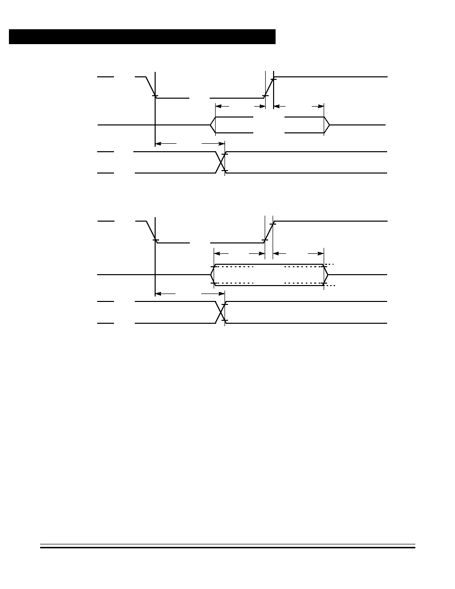
Technical Data
M68HC11K Family
258
Electrical Characteristics
MOTOROLA
Electrical Characteristics
Figure 12-1. Test Methods
CLOCKS,
STROBES
INPUTS
~ V
DD
SPEC
OUTPUTS
AC TESTING
~ V
SS
~ V
DD
CLOCKS,
STROBES
INPUTS
0.4 VOLTS
~ V
DD
70% OF V
DD
V
DD
� 0.8 VOLTS
0.4 VOLTS
OUTPUTS
0.4 VOLTS
DC TESTING
~ V
SS
V
DD
� 0.8 VOLTS
NOMINAL
20% OF V
DD
~ V
DD
20% OF V
DD
70% OF V
DD
20% OF V
DD
V
DD
� 0.8 VOLTS
0.4 VOLTS
70% OF V
DD
20% OF V
DD
~ V
SS
20% OF V
DD
70% OF V
DD
SEE NOTE 2
Notes:
1.
Full test loads are applied during all DC electrical tests and AC timing measurements.
2.
During AC timing measurements, inputs are driven to 0.4 volts and V
DD
� 0.8 volts while timing
measurements are taken at the 20% and 70% of V
DD
points.
TIMING
NOMINAL
TIMING
NOMINAL
TIMING
TIMING
SPEC
TIMING
SPEC
TIMING
~ V
SS
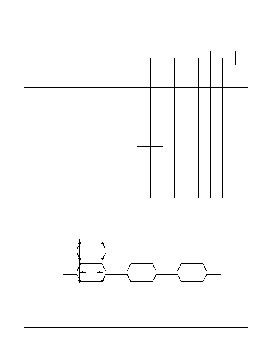
Electrical Characteristics
Control Timing
M68HC11K Family
Technical Data
MOTOROLA
Electrical Characteristics
259
12.8 Control Timing
Figure 12-2. Timer Inputs
Characteristic
(1)
1. V
DD
= 4.5 to 5.5 Vdc for standard devices, V
SS
= 0 Vdc, T
A
= T
L
to T
H
All timing measurements refer to 20% V
DD
and 70% V
DD
, unless otherwise noted.
Symbol
1.0 MHz
2.0 MHz
3.0 MHz
4.0 MHz
Unit
Min
Max Min Max Min Max Min
Max
Frequency of operation
f
o
dc
1.0
dc
2.0
dc
3.0
dc
4.0
MHz
E-clock period
t
cyc
1000
--
500
--
333
--
250
--
ns
Crystal frequency
f
XTAL
--
4.0
--
8.0
--
12.0
--
16.0 MHz
External oscillator frequency
4 f
o
dc
4.0
dc
8.0
dc
12.0
dc
16.0 MHz
Processor control setup time
t
PCSU
= 1/4 t
cyc
+ 50 ns
t
PCSU
= 1/4 t
cyc
+ 75 ns
(extended voltage devices)
t
PCSU
300
325
--
--
175
200
--
--
133
158
--
--
112
--
--
--
ns
Reset input pulse width
(2)
To guarantee external reset vector
Minimum input time
(3)
2. Reset is recognized during the first clock cycle it is held low. Internal circuitry then drives the pin low for eight clock cycles,
releases the pin, and samples the pin level two cycles later to determine the source of the interrupt.
3. Can be pre-empted by internal reset
PW
RSTL
16
1
--
--
16
1
--
--
16
1
--
--
16
1
--
--
t
cyc
Mode programming setup time
t
MPS
2
--
2
--
2
--
2
--
t
cyc
Mode programming hold time
t
MPH
10
--
10
--
10
--
10
--
ns
Interrupt pulse width,
IRQ edge-sensitive mode
PW
IRQ
= t
cyc
+ 20 ns
PW
IRQ
1020
--
520
--
353
--
270
--
ns
Wait recovery startup time
t
WRS
--
4
--
4
--
4
--
4
t
cyc
Timer pulse width
PW
TIM
= t
cyc
+ 20 ns
Input capture, pulse accumulator
PW
TIM
1020
--
520
--
353
--
270
--
ns
PA7
2,3
PA7
1,3
PA[3:0]
2
PA[3:0]
1
Notes:
1. Rising edge sensitive input
2. Falling edge sensitive input
3. Maximum pulse accumulator clocking rate is E-clock frequency divided by 2.
PW
TIM
T
e
c
hni
c
a
l
Dat
a
M
6
8HC1
1K
F
a
m
i
l
y
260
E
l
ec
t
r
i
c
al
Charac
t
e
r
i
s
t
i
c
s
M
O
T
O
R
OLA
E
l
ec
tr
ic
al C
h
a
r
a
c
t
e
r
i
st
ics
Figure 12-3. POR External Reset Timing Diagram
t
PCSU
ADDRESS
MODA, MODB
E
EXTAL
V
DD
RESET
4064 t
CYC
FFFE
FFFE
FFFE
NEW
PC
FFFE
FFFF
FFFE
FFFE
FFFE
NEW
PC
FFFE
FFFF
FFFE
t
MPH
PW
RSTL
t
MPS
M
68HC1
1K
F
a
m
i
l
y
T
e
c
hni
c
a
l
Dat
a
M
O
T
O
ROL
A
E
l
ec
t
r
i
c
al
Charac
t
e
r
i
s
t
i
c
s
261
E
l
ec
t
r
i
c
al
Charac
t
e
ri
s
t
i
c
s
Co
nt
rol
T
i
m
i
ng
Figure 12-4. STOP Recovery Timing Diagram
PW
IRQ
t
STOPDELAY
3
IRQ
1
IRQ
2
OR XIRQ
E
SP � 8
SP � 8
FFF2
(FFF4)
NEW
PC
STOP
ADDR
STOP
ADDR + 1
ADDRESS
4
STOP
ADDR
STOP
ADDR + 1
STOP
ADDR + 1
STOP
ADDR + 1
STOP
ADDR + 2 SP...SP�7
FFF3
(FFF5)
OPCODE
RESUME PROGRAM WITH INSTRUCTION
INTERNAL
ADDRESS
5
CLOCKS
Notes:
1. Edge-sensitive IRQ pin (IRQE bit = 1)
2. Level-sensitive IRQ pin (IRQE bit = 0)
3. t
STOPDELAY
= 4064 t
cyc
if DLY bit = 1 or 4 t
cyc
if DLY = 0
4. XIRQ with X bit in CCR = 1
5. IRQ or XIRQ with X bit in CCR = 0
WHICH FOLLOWS THE STOP INSTRUCTION.

T
e
c
hni
c
a
l
Dat
a
M
6
8HC1
1K
F
a
m
i
l
y
262
E
l
ec
t
r
i
c
al
Charac
t
e
r
i
s
t
i
c
s
M
O
T
O
R
OLA
E
l
ec
tr
ic
al C
h
a
r
a
c
t
e
r
i
st
ics
Figure 12-5. WAIT Recovery from Inerrupt Timing Diagram
Figure 12-6. Interrupt Timing Diagram
ADDR + 1
t
PCSU
PCL, PCH, YL, YH, XL,
E
R/W
ADDRESS
WAIT
ADDR
WAIT
ADDR + 1
SP
SP � 1
SP � 2...SP � 8
SP � 8
SP � 8...SP � 8
SP � 8
SP � 8
SP � 8
VECTOR
ADDR
VECTOR
NEW
PC
t
WRS
Note: RESET also causes recovery from WAIT.
IRQ, XIRQ,
OR INTERNAL
INTERRUPTS
XH, A, B, CCR
STACK REGISTERS
E
PW
IRQ
SP � 8
SP � 8
ADDRESS
NEW
PC
NEXT
OPCODE
NEXT
OP + 1
IRQ
1
VECTOR
ADDR
SP � 7
t
PCSU
IRQ
2
, XIRQ,
OR INTERNAL
INTERRUPT
SP
SP � 1
SP � 2
SP � 3
SP � 4
SP � 5
SP � 6
VECTOR
ADDR + 1
OP
CODE
� �
DATA
PCL
PCH
IYL
IYH
IXL
IXH
B
A
CCR
� �
VECT
MSB
VECT
LSB
OP
CODE
R/W
Notes:
1. Edge-sensitive IRQ pin (IRQE bit = 1)
2. Level-sensitive IRQ pin (IRQE bit = 0)
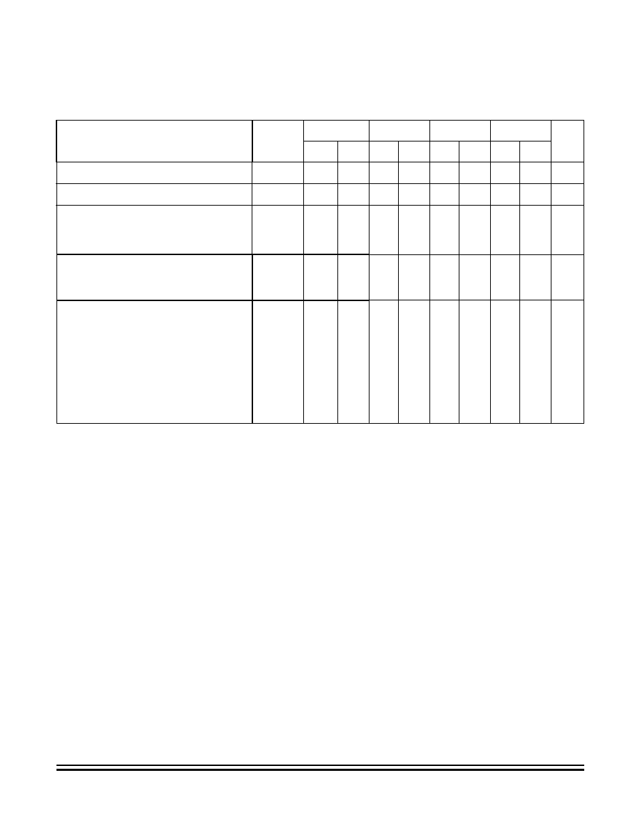
Electrical Characteristics
Peripheral Port Timing
M68HC11K Family
Technical Data
MOTOROLA
Electrical Characteristics
263
12.9 Peripheral Port Timing
Characteristic
(1)
1. V
DD
= 4.5 to 5.5 Vdc for standard devices, V
SS
= 0 Vdc, T
A
= T
L
to T
H
All timing measurements refer to 20% V
DD
and 70% V
DD
, unless otherwise noted.
Symbol
1.0 MHz
2.0 MHz
3.0 MHz
4.0 MHz
Unit
Min
Max
Min
Max
Min
Max
Min
Max
Frequency of operation (E clock)
f
o
dc
1.0
dc
2.0
dc
3.0
dc
4.0
MHz
E-clock period
t
cyc
1000
--
500
--
333
--
250
--
ns
Peripheral data setup time
(2)
MCU read of ports A, B, C, D, E,
F, G, and H
2. Ports C and D timing is valid only in active drive mode. (CWOM and DWOM bits are cleared in OPT2 and SPCR registers,
respectively.)
t
PDSU
100
100
100
100
ns
Peripheral data hold time
MCU read of ports A, B, C, D, E,
F, G, and H
t
PDH
50
--
50
--
50
--
50
--
ns
Delay time, peripheral data write
Standard devices
MCU write to port A, B, G, and H
MCU write to ports C, D, and F
(t
PWD
= 1/4 t
cyc
+ 100 ns)
Extended voltage
MCU write to port A, B, G, and H
MCU write to ports C, D, and F
(t
PWD
= 1/4 t
cyc
+ 150 ns)
t
PWD
--
--
--
--
200
350
250
400
--
--
--
--
200
225
250
225
--
--
--
--
200
183
250
233
--
--
--
--
200
162
--
--
ns
Technical Data
M68HC11K Family
264
Electrical Characteristics
MOTOROLA
Electrical Characteristics
Figure 12-7. Port Read Timing Diagram
Figure 12-8. Port Write Timing Diagram
MCU READ OF PORT
t
PDSU
t
PDSU
t
PDH
t
PDH
E
PORTS A, C, D, F
PORTS B, E, G
MCU WRITE TO PORT
t
PWD
E
PORTS C, D, F
PORTS A, B, G, H
t
PWD
PREVIOUS PORT DATA
PREVIOUS PORT DATA
NEW DATA VALID
NEW DATA VALID
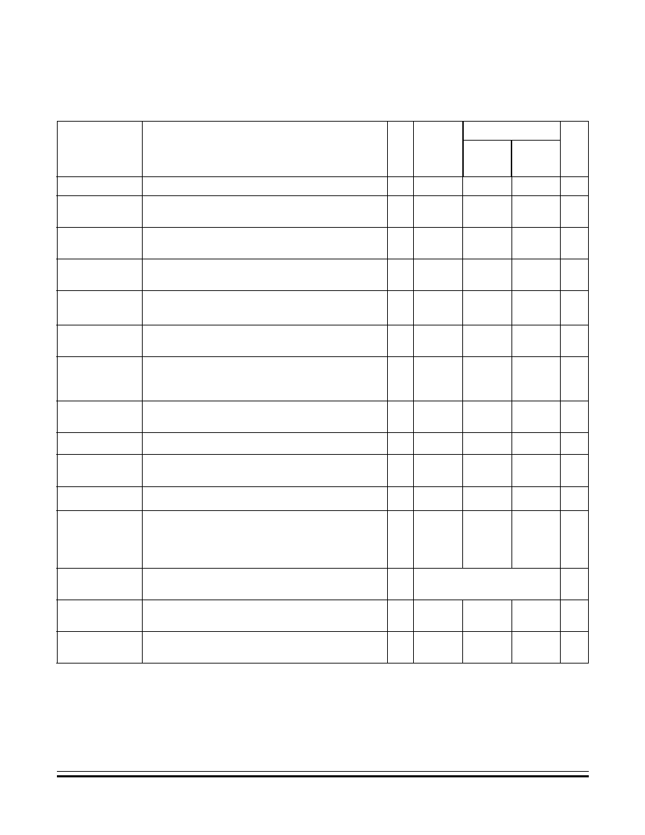
Electrical Characteristics
Analog-to-Digital Converter Characteristics
M68HC11K Family
Technical Data
MOTOROLA
Electrical Characteristics
265
12.10 Analog-to-Digital Converter Characteristics
Characteristic
(1)
Parameter
Min Absolute
Max
Unit
f
o
2.0
MHz
f
o
> 2.0
MHz
(2)
Resolution
Number of bits resolved by A/D converter
--
8
--
--
Bits
Non-linearity
Maximum deviation from the ideal A/D
transfer characteristics
--
--
�
1/2
�
1
LSB
Zero error
Difference between the output of an ideal and an
actual for zero input voltage
--
--
�
1/2
�
1
LSB
Full scale
error
Difference between the output of an ideal and an
actual A/D for full-scale input voltage
--
--
�
1/2
�
1
LSB
Total unadjusted
error
Maximum sum of non-linearity, zero error, and
full-scale error
(3)
--
--
�
1/2
�
1 1/2
LSB
Quantization
error
Uncertainty because of converter resolution
--
--
�
1/2
�
1/2
LSB
Absolute
accuracy
Difference between the actual input voltage and the
full-scale weighted equivalent of the binary output
code, all error sources included
--
--
�
1
�
2
LSB
Conversion
range
Analog input voltage range
V
RL
--
V
RH
V
RH
V
V
RH
Maximum analog reference voltage
(3)
V
RL
--
V
DD
+ 0.1 V
DD
+ 0.1
V
V
RL
Minimum analog reference voltage
(3)
V
SS
�
0.1
--
V
RH
V
RH
V
V
R
Minimum difference between V
RH
and V
RL
(3)
3
--
--
--
V
Conversion
time
Total time to perform a single analog-to-digital
conversion:
E clock
Internal RC oscillator
--
--
32
--
--
t
cyc
+ 32
--
t
cyc
+ 32
t
cyc
�
s
Monotonicity
Conversion result never decreases with an increase
in input voltage and has no missing codes
Guaranteed
Zero Input
reading
Conversion result when V
In
= V
RL
00
--
--
--
Hex
Full Scale
reading
Conversion result when V
In
= V
RH
--
--
FF
FF
Hex
Continued

Technical Data
M68HC11K Family
266
Electrical Characteristics
MOTOROLA
Electrical Characteristics
Sample
acquisition time
Analog input acquisition sampling time:
E Clock
Internal RC Oscillator
--
--
12
--
--
12
--
12
t
cyc
�
s
Sample/hold
capacitance
Input capacitance during sample PE[7:0]
--
20 (Typ)
--
--
pF
Input leakage
Input leakage on A/D pins
PE[7:0]
V
RL
, V
RH
--
--
--
--
400
1.0
400
1.0
nA
�
A
1. V
DD
= 4.5 to 5.5 Vdc for standard devices; V
SS
= 0 Vdc, T
A
= T
L
to T
H
Source impedances greater than 10 k
affect
accuracy adversely because of input leakage.
All timing measurements refer to 20% V
DD
and 70% V
DD
, unless otherwise noted.
2. Up to 4.0 MHz for standard devices.
3. Performance is verified down to 2.5 V
V
R
, but accuracy is tested and guaranteed at
V
R
= 5 V
�
10%.
Characteristic
(1)
Parameter
Min Absolute
Max
Unit
f
o
2.0
MHz
f
o
> 2.0
MHz
(2)
Electrical Characteristics
Expansion Bus Timing
M68HC11K Family
Technical Data
MOTOROLA
Electrical Characteristics
267
12.11 Expansion Bus Timing
Num
Characteristic
(1)
1. V
DD
= 5.0
�
10%, V
SS
= 0 Vdc, T
A
= T
L
to T
H
, unless otherwise noted
All timing measurements refer to 20% V
DD
and 70% V
DD
, unless otherwise noted.
Symbol
2.0 MHz
3.0 MHz
4.0 MHz
Unit
Min
Max
Min
Max
Min
Max
Frequency of operation (E clock)
(2)
2. Input clocks with duty cycles other than 50% affect bus performance.
f
o
dc
2.0
dc
3.0
dc
4.0
MHz
1
Cycle time, t
cyc
= 1/f
o
t
cyc
500
-- 333
--
250
--
ns
2
Pulse width, E low, PW
EL
= 1/2 t
cyc
� 20 ns
PW
EL
230
--
147
--
105
--
ns
3
Pulse width, E high
(3)
PW
EH
= 1/2 t
cyc
�
25 ns
3. This parameter is affected by clock stretching. Add n(t
cyc
) to parameter value, where n = 1, 2, or 3 depending on values
written to CSCSTR register or n = 1 for STRCH = 1 on KS parts.
PW
EH
225
--
142
--
100
--
ns
4A
4B
E clock
Rise time
Fall time
t
r
t
f
--
--
20
20
--
--
20
18
--
--
20
15
ns
9
Address hold time, t
AH
= 1/8 t
cyc
�
10 ns
t
AH
53
--
32
--
21
--
ns
11
Address delay time, t
AD
= 1/8 t
cyc
+
40 ns
t
AD
--
103
--
82
--
71
ns
12
Address valid time to E rise
t
AV
= PW
EL
�
t
AD
t
AV
128
--
65
--
34
--
ns
17
Read data setup time
t
DSR
30
--
30
--
20
--
ns
18
Read data hold time
t
DHR
0
--
0
--
0
--
ns
19
Write data delay time
t
DDW
--
40
--
40
--
40
ns
21
Write data hold time, t
DHW
= 1/8 t
cyc
t
DHW
63
--
42
--
31
--
ns
29
MPU address access time
(3)
t
ACCA
= t
cyc
�
t
f
� t
DSR
�
t
AD
t
ACCA
348
--
203
--
144
--
ns
39
Write data setup time
(3)
t
DSW
= PW
EH
�
t
DDW
t
DSW
185
--
102
--
60
--
ns
50
E valid chip-select delay time
t
ECSD
--
40
--
40
--
40
ns
51
E valid chip-select access time
(3)
t
ECSA
= PW
EH
�
t
ECSD
�
t
DSR
t
ECSA
155
--
72
--
40
--
ns
52
Chip select hold time
t
CH
0
20
0
20
0
20
ns
54
Address valid chip-select delay time
t
ACSD
= 1/4 t
cyc
+ 40 ns
t
ACSD
--
165
--
123
--
103
ns
55
Address valid chip-select access time
t
ACSA
= t
cyc
� t
f
� t
DSR
�
t
ACSD
(3)
t
ACSA
285
--
162
--
113
--
ns
56
Address valid to chip-select time
t
AVCS
10
--
10
--
10
--
ns
57
Address valid to data three-state time
t
AVDZ
--
10
--
10
--
10
ns

Technical Data
M68HC11K Family
268
Electrical Characteristics
MOTOROLA
Electrical Characteristics
Figure 12-9. Expansion Bus Timing
E
R/W, ADDRESS
READ DATA
WRITE DATA
CS E VALID
CS AD VALID
11
2
1
3
12
17
29
19
50
51
39
55
54
4B
9
18
21
52
56
57
4A
Electrical Characteristics
Serial Peripheral Interface Timing
M68HC11K Family
Technical Data
MOTOROLA
Electrical Characteristics
269
12.12 Serial Peripheral Interface Timing
Num
Characteristic
(1)
1. V
DD
= 4.5 to 5.5 Vdc, V
SS
= 0 Vdc, T
A
= T
L
to T
H
. All timing measurements refer to 20% V
DD
and 70% V
DD
, unless
otherwise noted.
Symbol
Min
Max
Unit
Operating frequency
Master
Slave
f
op(m)
f
op(s)
f
o
/128
dc
f
o
/2
f
o
MHz
1
Cycle time
Master
Slave
t
cyc(m)
t
cyc(s)
2
1
128
--
t
cyc
2
Enable lead time
Slave
t
Lead(s)
1
--
t
cyc
3
Enable lag time
Slave
t
Lag(s)
1
--
t
cyc
4
Clock (SCK) high time
Master
Slave
t
w(SCKH)m
t
w(SCKH)s
t
cyc
� 25
1/2 t
cyc
� 25
64 t
cyc
--
ns
5
Clock (SCK) low time
Master
Slave
t
w(SCKL)m
t
w(SCKL)s
t
cyc
� 25
1/2 t
cyc
� 25
64 t
cyc
--
ns
6
Data setup time (inputs)
Master
Slave
t
su(m)
t
su(s)
30
30
--
--
ns
7
Data hold time (inputs)
Master
Slave
t
h(m)
t
h(s)
30
30
--
--
ns
8
Slave access time (time to data active from high-impedance
state)
t
a
0
40
ns
9
Slave disable time (hold time
to high-impedance state)
t
dis
--
50
ns
10
Data valid (after enable edge)
(2)
2. Capacitive load on all SPI pins is 200 pF.
t
v(s)
--
50
ns
11
Data hold time (outputs) (after enable edge)
t
ho
0
--
ns
Technical Data
M68HC11K Family
270
Electrical Characteristics
MOTOROLA
Electrical Characteristics
a) SPI Master Timing (CPHA = 0)
b) SPI Master Timing (CPHA = 1)
Figure 12-10. SPI Timing Diagram (Sheet 1 of 2)
(SEE NOTE)
(SEE NOTE)
MSB IN
BIT 6 . . . . . . . 1
LSB IN
MASTER LSB OUT
BIT 6 . . . . . . . 1
MASTER MSB OUT
1
5
5
4
4
7
6
11
10
11 (REF)
(INPUT)
SCK (CPOL = 0)
OUTPUT
SCK (CPOL = 1)
OUTPUT
MISO
INPUT
MOSI
OUTPUT
Note: This first clock edge is generated internally but is not seen at the SCK pin.
SS
SS IS HELD HIGH ON MASTER
MSB IN
BIT 6 . . . . . . . 1
LSB IN
MASTER LSB OUT
BIT 6 . . . . . . . 1
MASTER MSB OUT
1
5
5
4
4
7
6
11
10
10 (REF)
(INPUT)
SCK (CPOL = 0)
OUTPUT
SCK (CPOL = 1)
OUTPUT
MISO
INPUT
MOSI
OUTPUT
Note: This last clock edge is generated internally but is not seen at the SCK pin.
SEE NOTE
SEE NOTE
SS IS HELD HIGH ON MASTER
SS
Electrical Characteristics
Serial Peripheral Interface Timing
M68HC11K Family
Technical Data
MOTOROLA
Electrical Characteristics
271
a) SPI Slave Timing (CPHA = 0)
b) SPI Slave Timing (CPHA = 1)
Figure 12-10. SPI Timing Diagram (Sheet 2 of 2)
SS
MSB IN
BIT 6 . . . . . . . 1
LSB IN
SLAVE LSB OUT
BIT 6 . . . . . . . 1
SLAVE MSB OUT
1
5
5
4
4
11
INPUT
SCK (CPOL = 0)
INPUT
SCK (CPOL = 1)
INTPUT
MOSI
INPUT
MISO
OUTPUT
Note: Not defined, but normally MSB of character just received
8
6
7
10
3
9
11
2
SEE
NOTE
MSB IN
BIT 6 . . . . . . . . 1
LSB IN
SLAVE LSB OUT
BIT 6 . . . . . . . . . . . 1
SLAVE MSB OUT
1
5
5
4
4
11
INPUT
SCK (CPOL = 0)
INPUT
SCK (CPOL = 1)
INTPUT
MOSI
INPUT
MISO
OUTPUT
Note: Not defined, but normally LSB of character previously transmitted
6
7
10
9
2
SEE
NOTE
8
10
3
SS

Technical Data
M68HC11K Family
272
Electrical Characteristics
MOTOROLA
Electrical Characteristics
12.13 EEPROM Characteristics
Characteristic
(1)
1. V
DD
= 5.0 Vdc
�
10%, V
SS
= 0 Vdc, T
A
= T
L
to T
H
Temperature Range
Unit
�40 to 85
�
C
�40 to 105
�
C
�40 to 125
�
C
Programming time
<
1.0 MHz, RCO enabled
(2)
1.0 to 2.0 MHz, RCO disabled
2.0 MHz (or anytime RCO enabled)
2. The RC oscillator (RCO) must be enabled (by setting the CSEL bit in the OPTION register) for EEPROM programming and
erasure when the E-clock frequency is below 1.0 MHz.
10
20
10
15
Must use RCO
15
20
Must use RCO
20
ms
Erase time
(2)
Byte, row, and bulk
10
10
10
ms
Write/erase endurance
(3)
3. Refer to Reliability Monitor Report (current quarterly issue) for current failure rate information.
10,000
10,000
10,000
Cycles
Data retention
(3)
10
10
10
Years

M68HC11K Family
Technical Data
MOTOROLA
Mechanical Data
273
Technical Data -- M68HC11K Family
Section 13. Mechanical Data
13.1 Contents
13.2
Introduction . . . . . . . . . . . . . . . . . . . . . . . . . . . . . . . . . . . . . . . 273
13.3
84-Pin Plastic-Leaded Chip Carrier (Case 780) . . . . . . . . . . . 275
13.4
84-Pin J-Cerquad (Case 780A) . . . . . . . . . . . . . . . . . . . . . . .276
13.5
80-Pin Quad Flat Pack (Case 841B) . . . . . . . . . . . . . . . . . . . 277
13.6
80-Pin Low-Profile Quad Flat Pack (Case 917A) . . . . . . . . . . 278
13.7
68-Pin Plastic Leaded Chip Carrier (Case 779) . . . . . . . . . . . 279
13.8
68-Pin J-Cerquad (Case 779A) . . . . . . . . . . . . . . . . . . . . . . .280
13.2 Introduction
The M68HC11K series microcontrollers are available in:
�
84-pin plastic-leaded chip carrier (PLCC)
�
84-pin J-cerquad (ceramic windowed version of PLCC)
�
80-pin quad flat pack (QFP)
�
80-pin low-profile quad flat pack (LQFP)
�
68-pin PLCC
�
68-pin J-cerquad

Technical Data
M68HC11K Family
274
Mechanical Data
MOTOROLA
Mechanical Data
The diagrams included in this section show the latest package
specifications available at the time of this publication. To make sure that
you have the latest information, contact one of the following:
�
Local Motorola Sales Office
�
World Wide Web at
http://www.motorola.com/semiconductors
Follow the World Wide Web on-line instructions to retrieve the current
mechanical specifications.
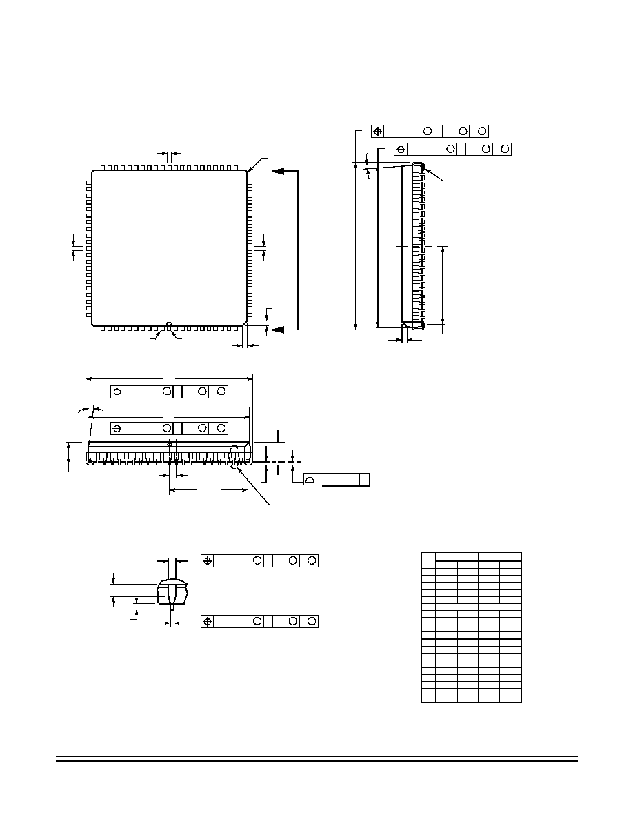
Mechanical Data
84-Pin Plastic-Leaded Chip Carrier (Case 780)
M68HC11K Family
Technical Data
MOTOROLA
Mechanical Data
275
13.3 84-Pin Plastic-Leaded Chip Carrier (Case 780)
NOTES:
1.
DATUMS L, M, AND N DETERMINED WHERE TOP OF LEAD
SHOULDER EXITS PACKAGE BODY AT MOLD PARTING LINE.
2.
DIMENSION G1 TO BE MEASURED AT CLOSEST APPROACH
OF LEAD TO DATUM T, SEATING PLANE.
3.
DIMENSIONS R AND U DO NOT INCLUDE MOLD FLASH.
ALLOWABLE MOLD FLASH IS 0.010 (0.25) PER SIDE.
4.
DIMENSIONING AND TOLERANCING PER ANSI Y14.5M, 1982.
5.
CONTROLLING DIMENSION: INCH.
6.
THE PACKAGE TOP MAY BE SMALLER THAN THE PACKAGE
BOTTOM BY UP TO 0.012 (0.300). DIMENSIONS R AND U ARE
DETERMINED AT THE OUTERMOST EXTREMES OF THE
PLASTIC BODY EXCLUSIVE OF MOLD FLASH, TIE BAR
BURRS, GATE BURRS AND INTERLEAD FLASH, BUT
INCLUDING ANY MISMATCH BETWEEN THE TOP AND
BOTTOM OF THE PLASTIC BODY.
7.
DIMENSION H DOES NOT INCLUDE DAMBAR PROTRUSION
OR INTRUSION. THE DAMBAR PROTRUSION(S) SHALL NOT
CAUSE THE H DIMENSION TO BE GREATER THAN 0.037
(0.94). THE DAMBAR INTRUSION(S) SHALL NOT CAUSE THE
H DIMENSION TO BE SMALLER THAN 0.025 (0.635).
-L-
-M-
-N-
Y
BRK
W
D
D
V
84
1
A
R
G
G1
C
Z
J
E
VIEW S
0.004 (0.10)
-T-
SEATING
PLANE
S
L-M
M
0.007 (0.18)
T
S
N
B
U
Z
2X
X
VIEW D-D
H
K1
K
F
VIEW S
DIM
MIN
MAX
MIN
MAX
MILLIMETERS
INCHES
A
1.185
1.195
30.10
30.35
B
1.185
1.195
30.10
30.35
C
0.165
0.180
4.20
4.57
E
0.090
0.120
2.29
3.05
F
0.013
0.021
0.33
0.53
G
0.050 BSC
1.27 BSC
H
0.026
0.032
0.66
0.81
J
0.020
---
0.51
---
K
0.025
---
0.64
---
R
1.150
1.156
29.21
29.36
U
1.150
1.156
29.21
29.36
V
0.042
0.048
1.07
1.21
W
0.042
0.048
1.07
1.21
X
0.042
0.056
1.07
1.42
Y
---
0.020
---
0.50
Z
2
10
2
10
G1 0.545
0.565
13.84
14.35
K1 0.060
---
1.52
---
�
�
�
�
S
L-M
M
0.007 (0.18)
T
S
N
S
L-M
S
0.007 (0.18)
T
S
N
S
L-M
S
0.007 (0.18)
T
S
N
S
L-M
S
0.007 (0.18)
T
S
N
S
L-M
S
0.007 (0.18)
T
S
N
2X
T
G1
84X R
R1
R1 0.025
0.045
0.64
1.14
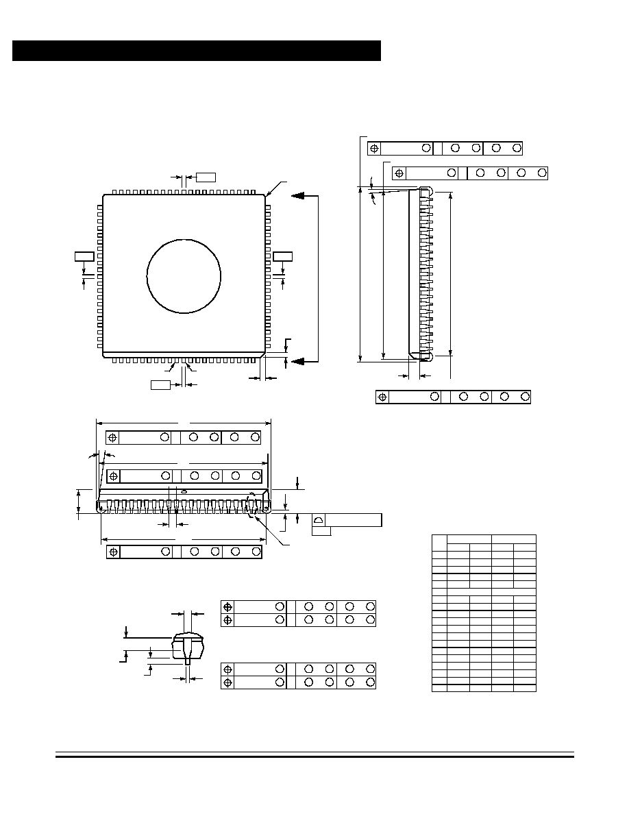
Technical Data
M68HC11K Family
276
Mechanical Data
MOTOROLA
Mechanical Data
13.4 84-Pin J-Cerquad (Case 780A)
NOTES:
1.
DATUMS -L-, -M-, -N-, AND -P- DETERMINED WHERE TOP
OF LEAD SHOULDER EXITS PACKAGE BODY AT GLASS
PARTING LINE.
2.
DIMENSION G1, TRUE POSITION TO BE MEASURED AT
DATUM -T-, SEATING PLANE.
3.
DIMENSIONS R AND U DO NOT INCLUDE GLASS
PROTRUSION. ALLOWABLE GLASS PROTRUSION IS
0.25 (0.010) PER SIDE.
4.
DIMENSIONING AND TOLERANCING PER ANSI Y14.5M,
1982.
5.
CONTROLLING DIMENSION: INCH.
-L-
-M-
-P-
-N-
Y
BRK
W
D
D
V
84
1
S
L
M
0.18 (0.007)
-M
S
T
S
N
-P
S
S
L
M
0.18 (0.007)
-M
S
T
S
N
-P
S
A
R
G
G1
S
L
S
0.25 (0.010)
-M
S
T
S
N
-P
S
C
Z
J
E
DETAIL S
0.100 (0.004)
-T-
SEATING
PLANE
S
N
M
0.25 (0.010)
-P
S
T
S
L
-M
S
S
L
M
0.18 (0.007)
-M
S
T
S
N
-P
S
S
N
-P
S
M
0.18 (0.007)
T
S
L
-M
S
S
N
-P
S
M
0.18 (0.007)
T
S
L
-M
S
B
U
Z1
G1
X
DETAIL D-D
S
N
-P
S
M
0.18 (0.007)
T
S
L
-M
S
H
K1
K
F
DETAIL S
S
L
M
0.18 (0.007)
-M
S
T
S
N
-P
S
S
N
-P
S
M
0.18 (0.007)
T
S
L
-M
S
DIM
MIN
MAX
MIN
MAX
MILLIMETERS
INCHES
A
1.185
1.195
30.10
30.35
B
1.185
1.195
30.10
30.35
C
0.165
0.180
4.20
4.57
E
0.090
0.110
2.29
2.79
F
0.013
0.021
0.33
0.53
G
0.050 BSC
1.27 BSC
H
0.026
0.032
0.66
0.81
J
0.020
---
0.51
---
K
0.025
---
0.64
---
R
1.150
1.156
29.21
29.36
U
1.150
1.156
29.21
29.36
V
0.042
0.048
1.07
1.21
W
0.042
0.048
1.07
1.21
X
0.042
0.056
1.07
1.42
Y
---
0.020
---
0.50
Z
2
10
2
10
G1 1.110
1.130
28.20
28.70
K1 0.040
---
1.02
---
Z1
2
10
2
10
�
�
�
�
�
�
�
�
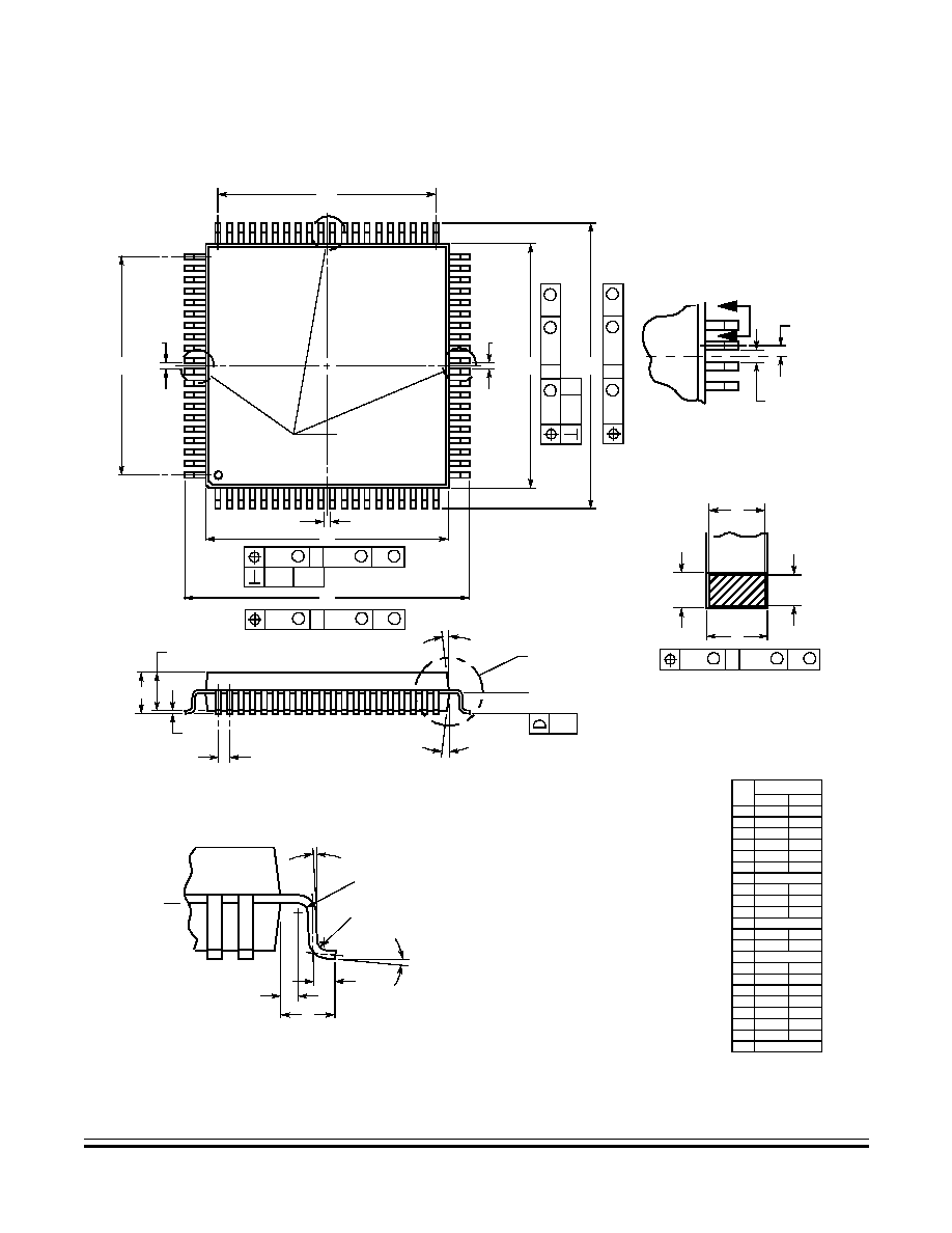
Mechanical Data
80-Pin Quad Flat Pack (Case 841B)
M68HC11K Family
Technical Data
MOTOROLA
Mechanical Data
277
13.5 80-Pin Quad Flat Pack (Case 841B)
NOTES:
1.
DIMENSIONING AND TOLERANCING PER ANSI
Y14.5M, 1982.
2.
CONTROLLING DIMENSION: MILLIMETER.
3.
DATUM PLANE -H- IS LOCATED AT BOTTOM OF LEAD
AND IS COINCIDENT WITH THE LEAD WHERE THE
LEAD EXITS THE PLASTIC BODY AT THE BOTTOM OF
THE PARTING LINE.
4.
DATUMS -A-, -B- AND -D- TO BE DETERMINED AT
DATUM PLANE -H-.
5.
DIMENSIONS S AND V TO BE DETERMINED AT
SEATING PLANE -C-.
6.
DIMENSIONS A AND B DO NOT INCLUDE MOLD
PROTRUSION. ALLOWABLE PROTRUSION IS 0.25
PER SIDE. DIMENSIONS A AND B DO INCLUDE MOLD
MISMATCH AND ARE DETERMINED AT DATUM PLANE
-H-.
7.
DIMENSION D DOES NOT INCLUDE DAMBAR
PROTRUSION. ALLOWABLE DAMBAR PROTRUSION
SHALL BE 0.08 TOTAL IN EXCESS OF THE D
DIMENSION AT MAXIMUM MATERIAL CONDITION.
DAMBAR CANNOT BE LOCATED ON THE LOWER
RADIUS OR THE FOOT.
SECTION B-B
61
60
DETAIL A
L
41
40
80
-A-
L
-D-
A
S
A-B
M
0.20
D
S
H
0.05 A-B
S
1
20
21
-B-
B
V
J
F
N
D
VIEW ROTATED 90
�
DETAIL A
B
B
P
-A-,-B-,-D-
E
H
G
M
M
DETAIL C
SEATING
PLANE
-C-
C
DATUM
PLANE
0.10
-H-
DATUM
PLANE
-H-
U
T
R
Q
K
W
X
DETAIL C
DIM
MIN
MAX
MILLIMETERS
A
13.90
14.10
B
13.90
14.10
C
2.15
2.45
D
0.22
0.38
E
2.00
2.40
F
0.22
0.33
G
0.65 BSC
H
---
0.25
J
0.13
0.23
K
0.65
0.95
L
12.35 REF
M
5
10
N
0.13
0.17
P
0.325 BSC
Q
0
7
R
0.13
0.30
S
16.95
17.45
T
0.13
---
U
0
---
V
16.95
17.45
W
0.35
0.45
X
1.6 REF
�
�
�
�
�
S
A-B
M
0.20
D
S
C
S
A-B
M
0.
2
0
D
S
H
0.
0
5
D
S
A-B
M
0.
20
D
S
C
S
A-B
M
0.20
D
S
C
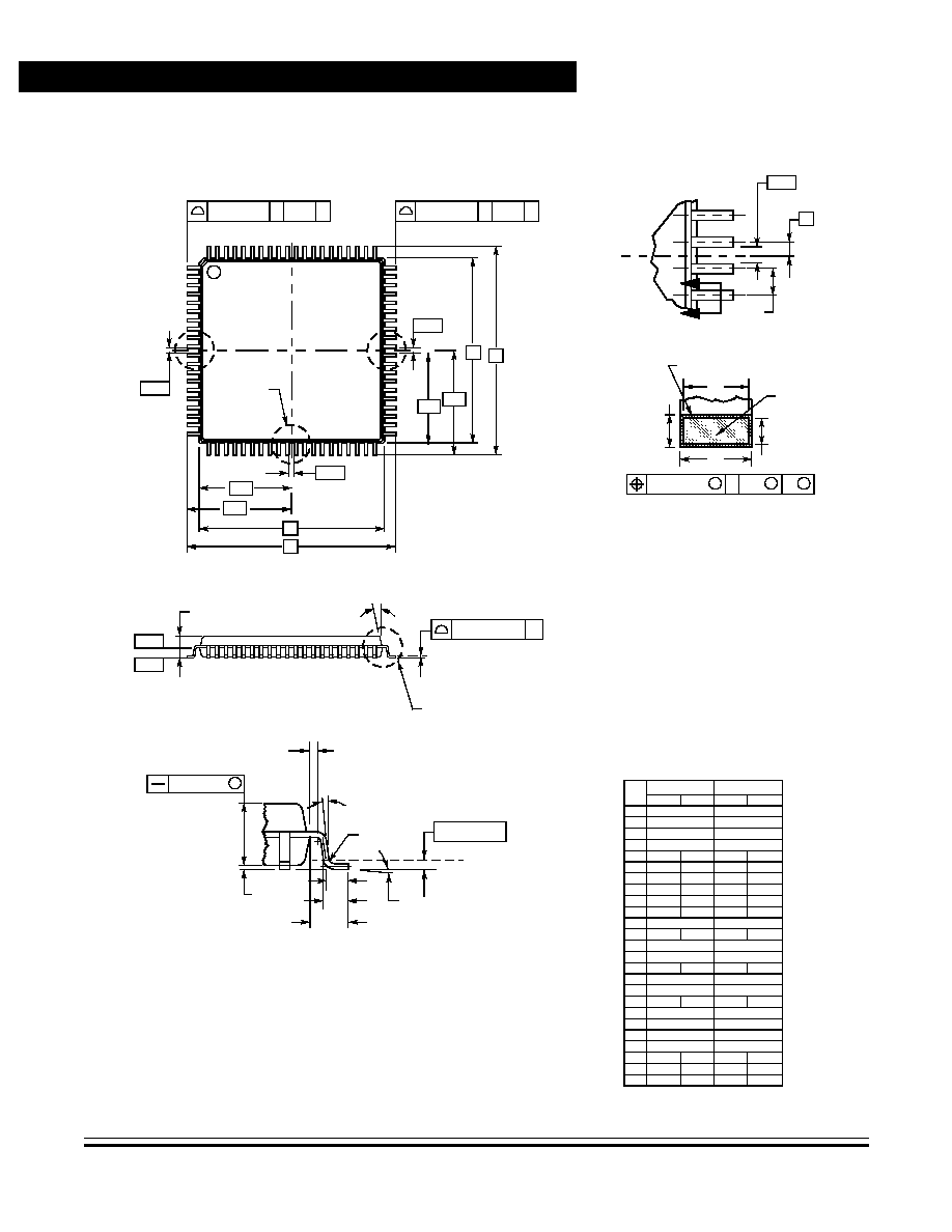
Technical Data
M68HC11K Family
278
Mechanical Data
MOTOROLA
Mechanical Data
13.6 80-Pin Low-Profile Quad Flat Pack (Case 917A)
1
20
21
40
41
60
61
80
VIEW AA
NOTES:
1.
DIMENSIONING AND TOLERANCING PER ANSI Y14.5M, 1982.
2.
CONTROLLING DIMENSION: MILLIMETER.
3.
DATUM PLANE -H- IS LOCATED AT BOTTOM OF LEAD AND IS
COINCIDENT WITH THE LEAD WHERE THE LEAD EXITS THE
PLASTIC BODY AT THE BOTTOM OF THE PARTING LINE.
4.
DATUMS -L-, -M- AND -N- TO BE DETERMINED AT DATUM
PLANE -H-.
5.
DIMENSIONS S AND V TO BE DETERMINED AT SEATING PLANE
-T-.
6.
DIMENSIONS A AND B DO NOT INCLUDE MOLD PROTRUSION.
ALLOWABLE PROTRUSION IS 0.250 (0.010) PER SIDE.
DIMENSIONS A AND B DO INCLUDE MOLD MISMATCH AND ARE
DETERMINED AT DATUM PLANE -H-.
7.
DIMENSION D DOES NOT INCLUDE DAMBAR PROTRUSION.
DAMBAR PROTRUSION SHALL NOT CAUSE THE LEAD WIDTH
TO EXCEED 0.460 (0.018). MINIMUM SPACE BETWEEN
PROTRUSION AND ADJACENT LEAD OR PROTRUSION 0.07
(0.003).
AB
VIEW Y
(K)
(Z)
(W)
VIEW AA
DIM
A
MIN
MAX
MIN
MAX
INCHES
14.00 BSC
0.551 BSC
MILLIMETERS
A1
7.00 BSC
0.276 BSC
B
14.00 BSC
0.551 BSC
B1
7.00 BSC
0.276 BSC
C
---
1.60
---
0.063
C1
0.04
0.24
0.002
0.009
C2
1.30
1.50
0.051
0.059
D
0.22
0.38
0.009
0.015
E
0.40
0.75
0.016
0.030
F
0.17
0.33
0.007
0.013
G
0.65 BSC
0.026 BSC
J
0.09
0.27
0.004
0.011
K
0.50 REF
0.020 REF
P
0.325 BSC
0.013 REF
R1
0.10
0.20
0.004
0.008
S
16.00 BSC
0.630 BSC
S1
8.00 BSC
0.315 BSC
U
0.09
0.16
0.004
0.006
V
16.00 BSC
0.630 BSC
V1
8.00 BSC
0.315 BSC
W
0.20 REF
0.008 REF
Z
1.00 REF
0.039 REF
0
01
---
---
02
C2
C1
C
L
0
10
0
9
14
0
10
0
9
14
�
�
�
�
�
�
�
�
�
�
L-M
0.20 (0.008)H
N
4X
3X
VIEW Y
-L-
L-M
0.20 (0.008)T
N
-M-
B
V
V1
B1
-N-
S1
A1
S
A
4X 20 TIPS
SEATING
0.10 (0.004) T
-H-
PLANE
-T-
q
8X
C
2
GAGE
0.25 (0.010)
PLANE
2X R
R1
E
q1
q
S
0.05 (0.002)
AB
-X-
X= L, M, N
P
G
PLATING
BASE
METAL
J
U
F
D
SECTION AB-AB
S
L-M
M
0.13 (0.005)
N
S
T
ROTATED 90 CLOCKWISE
�
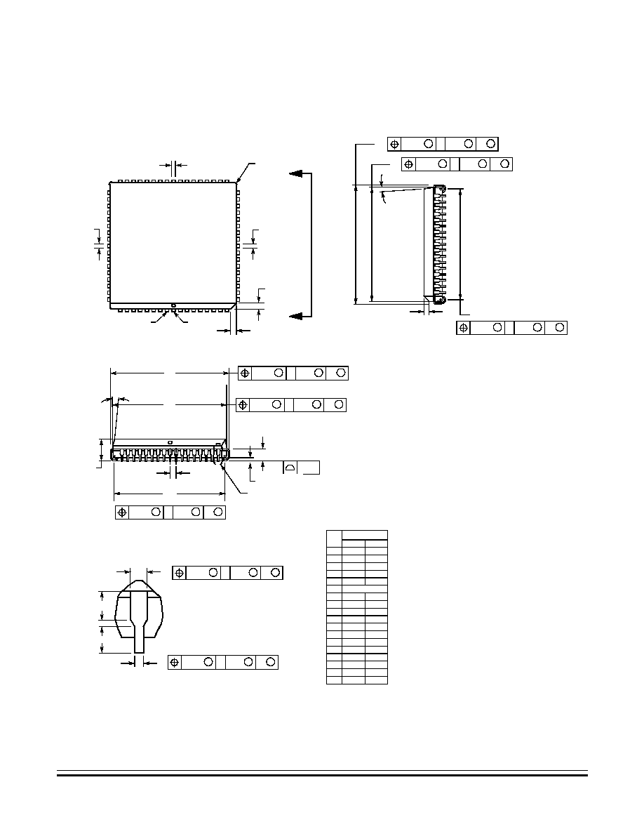
Mechanical Data
68-Pin Plastic Leaded Chip Carrier (Case 779)
M68HC11K Family
Technical Data
MOTOROLA
Mechanical Data
279
13.7 68-Pin Plastic Leaded Chip Carrier (Case 779)
NOTES:
1.
DATUMS L, M, AND N DETERMINED WHERE TOP
OF LEAD SHOULDER EXITS PLASTIC BODY AT
MOLD PARTING LINE.
2.
DIMENSION G1, TRUE POSITION TO BE
MEASURED AT DATUM T, SEATING PLANE.
3.
DIMENSIONS R AND U DO NOT INCLUDE MOLD
FLASH. ALLOWABLE MOLD FLASH IS 0.010 PER
SIDE.
4.
DIMENSIONING AND TOLERANCING PER ANSI
Y14.5M, 1982.
5.
CONTROLLING DIMENSION: INCH.
6.
THE PACKAGE TOP MAY BE SMALLER THAN THE
PACKAGE BOTTOM BY UP TO 0.012.
DIMENSIONS R AND U ARE DETERMINED AT THE
OUTERMOST EXTREMES OF THE PLASTIC
BODY EXCLUSIVE OF MOLD FLASH, TIE BAR
BURRS, GATE BURRS AND INTERLEAD FLASH,
BUT INCLUDING ANY MISMATCH BETWEEN THE
TOP AND BOTTOM OF THE PLASTIC BODY.
7.
DIMENSION H DOES NOT INCLUDE DAMBAR
PROTRUSION OR INTRUSION. THE DAMBAR
PROTRUSION(S) SHALL NOT CAUSE THE H
DIMENSION TO BE GREATER THAN 0.037. THE
DAMBAR INTRUSION(S) SHALL NOT CAUSE THE
H DIMENSION TO BE SMALLER THAN 0.025.
-N-
-L-
-M-
BRK
Y
W
V
D
D
68
1
A
R
G
G1
E
J
VIEW S
C
Z
S
L-M
M
0.007
N
S
T
0.004
-T-
SEATING
PLANE
X
Z
G1
VIEW D-D
U
B
DIM
MIN
MAX
INCHES
A
0.985
0.995
B
0.985
0.995
C
0.165
0.180
E
0.090
0.110
F
0.013
0.019
G
0.050 BSC
H
0.026
0.032
J
0.020
---
K
0.025
---
R
0.950
0.956
U
0.950
0.956
V
0.042
0.048
W
0.042
0.048
X
0.042
0.056
Y
---
0.020
Z
2
10
G1 0.910
0.930
K1 0.040
---
�
�
K1
K
F
H
VIEW S
S
L-M
M
0.007
N
S
T
S
L-M
S
0.010
N
S
T
S
L-M
M
0.007
N
S
T
S
L-M
M
0.007
N
S
T
S
L-M
M
0.007
N
S
T
S
L-M
M
0.007
N
S
T
S
L-M
S
0.010
N
S
T
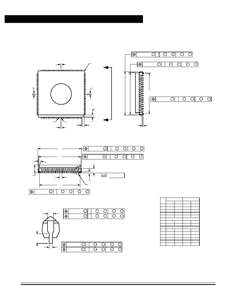
Technical Data
M68HC11K Family
280
Mechanical Data
MOTOROLA
Mechanical Data
13.8 68-Pin J-Cerquad (Case 779A)
NOTES:
1.
DATUMS -L-, -M-, -N-, AND -P- DETERMINED
WHERE TOP OF LEAD SHOULDER EXITS
PLASTIC BODY AT MOLD PARTING LINE.
2.
DIMENSION G1, TRUE POSITION TO BE
MEASURED AT DATUM -T-, SEATING
PLANE.
3.
DIMENSIONS R AND U DO NOT INCLUDE
MOLD FLASH. ALLOWABLE MOLD FLASH
IS 0.25 (0.010) PER SIDE.
4.
DIMENSIONING AND TOLERANCING PER
ANSI Y14.5M, 1982.
5.
CONTROLLING DIMENSION: INCH.
-N-
-L-
-M-
BRK
Y
W
V
D
D
68
1
A
R
G
G1
E
J
DETAIL S
C
0.010 (0.04)
-T-
SEATING
PLANE
G1
DETAIL D-D
U
B
K
F
H
DETAIL S
-P-
S
N
M
0.25 (0.010)
-P
S
T
S
L
-M
S
S
N
M
0.18 (0.007)
-P
S
T
S
L
-M
S
S
N
M
0.18 (0.007)
-P
S
T
S
L
-M
S
L
S
N
M
0.25 (0.010)
-P
S
T
S
L
-M
S
S
N
M
0.18 (0.007)
-P
S
T
S
L
-M
S
S
N
M
0.18 (0.007)
-P
S
T
S
L
-M
S
S
N
M
0.18 (0.007)
-P
S
T
S
L
-M
S
S
N
M
0.18 (0.007)
-P
S
T
S
L
-M
S
S
N
M
0.18 (0.007)
-P
S
T
S
L
-M
S
S
N
M
0.18 (0.007)
-P
S
T
S
L
-M
S
DIM
MIN
MAX
MIN
MAX
MILLIMETERS
INCHES
A
0.985
0.995
25.02
25.27
B
0.985
0.995
25.02
25.27
C
0.155
0.200
3.94
5.08
E
0.090
0.120
2.29
3.05
F
0.017
0.021
0.43
0.48
G
0.050 BSC
1.27 BSC
H
0.026
0.032
0.66
0.81
J
0.020
---
0.51
---
K
0.050 REF
1.27 REF
L
0.003
---
0.08
---
R
0.930
0.958
23.62
24.33
U
0.930
0.958
23.62
24.33
V
0.036
0.044
0.91
1.12
W
0.036
0.044
0.91
1.12
G1 0.890
0.930
22.61
23.62
Z
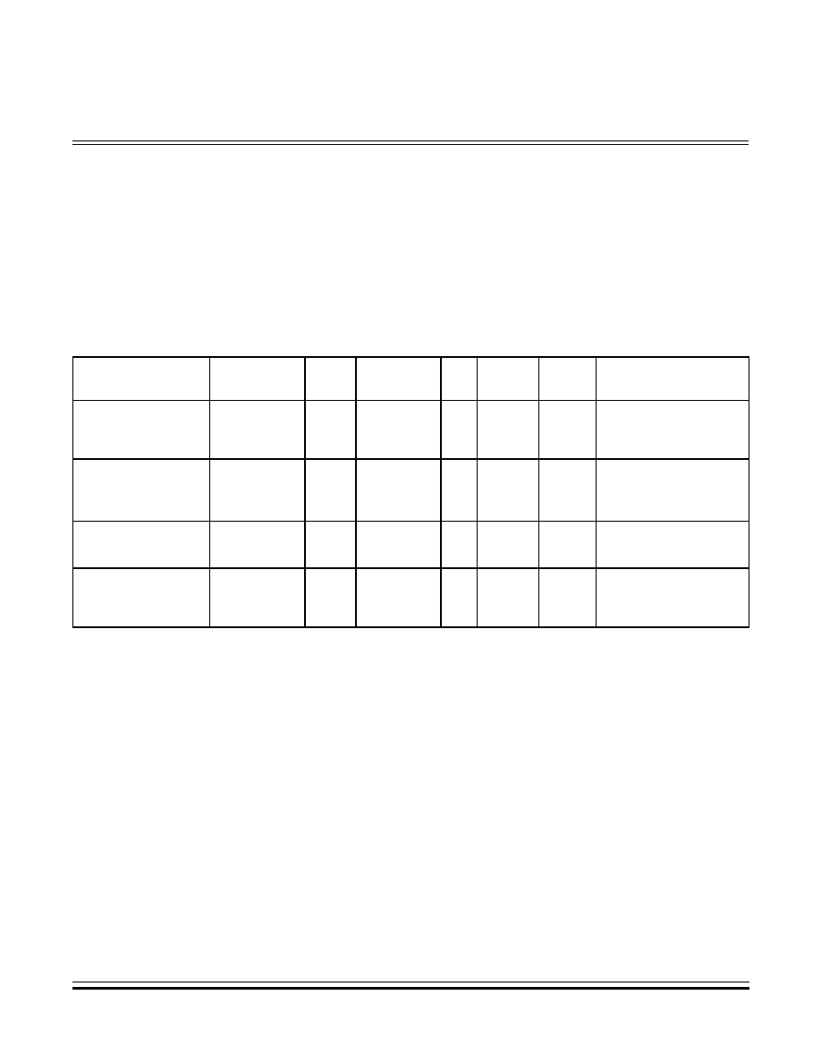
M68HC11K Family
Technical Data
MOTOROLA
Ordering Information
281
Technical Data -- M68HC11K Family
Section 14. Ordering Information
Use
Table 14-1
to determine part numbers when placing an order.
Table 14-1. M68HC11K Family Devices
Device
Number
ROM
or EPROM
RAM
EEPROM
I/O
Chip
Select
Slow
Mode
Packages
MC68HC(L)11K0
MC68HC(L)11K1
MC68HC(L)11K4
0
0
24 K
768
768
768
0
640
640
37
37
62
Yes
Yes
Yes
No
No
No
84-pin PLCC
(1)
80-pin QFP
(2)
MC68HC711K4
24 K
768
640
62
Yes
No
84-pin J-cerquad
(3)
84-pin PLCC
80-pin QFP
MC68HC11KS2
32 K
1 K
640
51
No
Yes
68-pin PLCC
80-pin LQFP
(4)
MC68HC711KS2
32 K
1 K
640
51
No
Yes
68-pin PLCC
80-pin LQFP
68-pin J-cerquad
1. PLCC = Plastic leaded chip carrier
2. QFP = Quad flat pack
3. J-cerquad = Ceramic windowed version of PLCC
4. LQFP = Low-profile quad flat pack

Technical Data
M68HC11K Family
282
Ordering Information
MOTOROLA
Ordering Information

M68HC11K Family
Technical Data
MOTOROLA
Development Support
283
Technical Data -- M68HC11K Family
Section 15. Development Support
Motorola has developed tools for use in debugging and evaluating
M68HC11 equipment. Specific development tools for use with the
M68HC11K series include:
�
M68HC11KEVS evaluation system
�
M68HC711KPGMR programmer board
�
M68HC711KEVB evaluation board
For more information about Motorola and third party development
system hardware and software, contact one of the following:
�
Local Motorola Sales Office
�
World Wide Web at
http://www.motorola.com/semiconductors

Technical Data
M68HC11K Family
284
Development Support
MOTOROLA
Development Support

M68HC11K Family
Technical Data
MOTOROLA
Index
285
Technical Data -- M68HC11K Family
Index
B
BAUD
Baud Rate
SCP[1:0]
SCI Baud Rate Prescaler Selects . . . . . . . . . . . . . .
159
C
CFORC
Timer Compare Force
FOC[1:5]
Force Output Comparison . . . . . . . . . . . . . . . . . . . .
201
CONFIG
System Configuration
NOCOP
ROM/PROM Enable . . . . . . . . . . . . . . . . . . . . . . . . .
108
ROMON
ROM/PROM Enable . . . . . . . . . . . . . . . . . . . . . . .
88
,
89
H
HPRIO
Highest Priority I-Bit Interrupt and Miscellaneous
MDA
Mode Select A . . . . . . . . . . . . . . . . . . . . . . . . . . . . . . . . .
81
PSEL[3:0]
Priority Select Bits . . . . . . . . . . . . . . . . . . . . . . . . .
123
RBOOT
Read Bootstrap ROM . . . . . . . . . . . . . . . . . . . . . . . . .
80
SMOD
Special Mode Select . . . . . . . . . . . . . . . . . . . . . . . . . . .
80
I
INIT
RAM and I/O Mapping Register
RAM[3:0]
RAM Map Position. . . . . . . . . . . . . . . . . . . . . . . . . . .
84
REG[3:0]
Register Block Position . . . . . . . . . . . . . . . . . . . . . . .
84
L
LIRDV LIR Driven . . . . . . . . . . . . . . . . . . . . . . . . . . . . . . . . . . . . . . .
40
O
OC1D
Output Compare 1 Data
OC1D[7:3]
Output Compare Masks. . . . . . . . . . . . . . . . . . . . .
203
OC1M
Output Compare 1 Mask
OC1M[7:3]
Output Compare 1 Masks . . . . . . . . . . . . . . . . . . .
202

Technical Data
M68HC11K Family
286
Index
MOTOROLA
Index
OPTION
System Configuration Options
CME
Clock Monitor Enable . . . . . . . . . . . . . . . . . . . . . . . . . . .
111
CR[1:0]
COP Timer Rate Select Bits. . . . . . . . . . . . . . . . . . . .
109
DLY
Enable Oscillator Startup Delay. . . . . . . . . . . . . . . . . . . .
132
IRQE
Configure IRQ for Edge-Sensitive Operation. . . . . . . . .
121
P
PACTL
Pulse Accumulator Control
I4/O5
Input Capture 4/Output Compare 5 . . . . . . . . . . . . . . . .
191
PAEN
Pulse Accumulator System Enable. . . . . . . . . . . . . . . .
205
PAMOD
Pulse Accumulator Mode . . . . . . . . . . . . . . . . . . . . .
206
RTR[1:0]
Real Time Interrupt Rate Select. . . . . . . . . . . . . . . .
210
PPROG
EPROM Programming Control
ELAT
PROM Latch Control . . . . . . . . . . . . . . . . . . . . . . . . . . . .
93
S
SCCR1
SCI Control Register 1
M
Mode (SCI Word Size). . . . . . . . . . . . . . . . . . . . . . . . . . . . .
160
WAKE
Wakeup mode . . . . . . . . . . . . . . . . . . . . . . . . . . . . . . . .
160
SCCR2
SCI Control Register 2
ILIE
Idle Line Interrupt Enable . . . . . . . . . . . . . . . . . . . . . . . . .
161
RE
Receiver Enable . . . . . . . . . . . . . . . . . . . . . . . . . . . . . . . .
162
RIE
Receiver Interrupt Enable. . . . . . . . . . . . . . . . . . . . . . . . .
161
RWU
Receiver Wakeup Control . . . . . . . . . . . . . . . . . . . . . . .
162
TCIE
Transmit Complete Interrupt Enable . . . . . . . . . . . . . . .
161
TE
Transmitter Enable. . . . . . . . . . . . . . . . . . . . . . . . . . . . . . .
162
TIE
Transmit Interrupt Enable . . . . . . . . . . . . . . . . . . . . . . . . .
161
SCI
Control Register 2
SBK
Send Break . . . . . . . . . . . . . . . . . . . . . . . . . . . . . . . . . . .
162
SCSR
SCI Status Register
FE
Framing Error Flag. . . . . . . . . . . . . . . . . . . . . . . . . . . . . . .
164
IDLE
Idle Line Detected Flag. . . . . . . . . . . . . . . . . . . . . . . . . .
163
NF
Noise Error Flag. . . . . . . . . . . . . . . . . . . . . . . . . . . . . . . . .
163
OR
Overrun Error Flag . . . . . . . . . . . . . . . . . . . . . . . . . . . . . .
163
RDRF
Receive Data Register Full Flag. . . . . . . . . . . . . . . . . .
163
TC
Transmit Complete Flag . . . . . . . . . . . . . . . . . . . . . . . . . .
163
TDRE
Transmit Data Register Empty Flag . . . . . . . . . . . . . . .
163

Index
M68HC11K Family
Technical Data
MOTOROLA
Index
287
SPCR
Serial Peripheral Control Register
CPHA
Clock Phase . . . . . . . . . . . . . . . . . . . . . . . . . . . . . . . . .
175
CPOL
Clock Polarity . . . . . . . . . . . . . . . . . . . . . . . . . . . . . . . .
175
DWOM
Port D Wired-OR Mode. . . . . . . . . . . . . . . . . . . . . . . .
174
MSTR
Master Mode Select . . . . . . . . . . . . . . . . . . . . . . . . . . .
174
SPE
Serial Peripheral System Enable. . . . . . . . . . . . . . . . . . .
174
SPR[1:0]
SPI Clock Rate Selects . . . . . . . . . . . . . . . . . . . . . .
175
SPSR
Serial Peripheral Status Register
MODF
Mode Fault . . . . . . . . . . . . . . . . . . . . . . . . . . . . . . . . . .
176
SPIF
SPI Transfer Complete Flag . . . . . . . . . . . . . . . . . . . . . .
176
WCOL
Write Collision . . . . . . . . . . . . . . . . . . . . . . . . . . . . . . .
176
T
TCTL1
Timer Control 1
OM[2:5]
Output Mode . . . . . . . . . . . . . . . . . . . . . . . . . . . . . . .
200
TCTL2
Timer Control 2
EDGxB and EDGxA
Input Capture Edge Control . . . . . . . . . .
195
TFLG1
Timer Interrupt Flag 1
I4/O5F
Input Capture 4/Output Compare 5 Flag . . . . . . .
194
,
199
IC1F�IC3F
Input Capture x Flag . . . . . . . . . . . . . . . . . . . . . . .
194
OC1F�OC4F
Output Compare x Flag . . . . . . . . . . . . . . . . . . .
199
TFLG2
Timer Interrupt Flag 2
PAIF
Pulse Accumulator Input Edge Flag . . . . . . . . . . . . . . . .
207
PAOVF
Pulse Accumulator Overflow Flag . . . . . . . . . . . . . . .
207
RTIF
Real-Time Interrupt Flag. . . . . . . . . . . . . . . . . . . . . . . . .
209
TOF
Timer Overflow Interrupt Flag . . . . . . . . . . . . . . . . . . . . .
189
TMSK1
Timer Interrupt Mask 1
I4/O5I
Input Capture 4
or Output Compare 5 Interrupt Enable . . . . . . .
195
,
200
IC1I�IC3I
Input Capture x Interrupt Enable . . . . . . . . . . . . . . .
194
OC1I�OC4
Output Compare x Interrupt Enable . . . . . . . . . . .
200
TMSK2
Timer Interrupt Mask 2
PR[1:0]
Timer Prescaler Select . . . . . . . . . . . . . . . . . . . . . . . .
190
RTII
Real-time Interrupt Enable. . . . . . . . . . . . . . . . . . . . . . . .
209
TOI
Timer Overflow Interrupt Enable. . . . . . . . . . . . . . . . . . . .
189

Technical Data
M68HC11K Family
288
Index
MOTOROLA
Index

blank

M68HC11K/D
M
68H11E S
eries
T
echnical Data
How to Reach Us:
USA/EUROPE/LOCATIONS NOT LISTED:
Motorola Literature Distribution
P.O. Box 5405
Denver, Colorado 80217
1-303-675-2140
1-800-441-2447
TECHNICAL INFORMATION CENTER:
1-800-521-6274
JAPAN:
Motorola Japan Ltd.
SPS, Technical Information Center
3-20-1, Minami-Azabu, Minato-ku
Tokyo 106-8573 Japan
81-3-3440-3569
ASIA/PACIFIC:
Motorola Semiconductors H.K. Ltd.
Silicon Harbour Centre
2 Dai King Street
Tai Po Industrial Estate
Tai Po, N.T., Hong Kong
852-26668334
HOME PAGE:
http://www.motorola.com/semiconductors/
Q4/00
REV 1