
WWW.MOTOROLA.COM/SEMICONDUCTORS
M68HC05
Microcontrollers
MC68HC705C8A/D
Rev. 3, 3/2002
MC68HC705C8A
MC68HSC705C8A
Technical Data

H8%'C8&$8'6√≤ Sr√"
√
Urpuvphy√9hh
HPUPSPG6
√"
MC68HC705C8A
MC68HSC705C8A
Technical Data
To provide the most up-to-date information, the revision of our
documents on the World Wide Web will be the most current. Your printed
copy may be an earlier revision. To verify you have the latest information
available, refer to:
http://www.motorola.com/semiconductors/
The following revision history table summarizes changes contained in
this document. For your convenience, the page number designators
have been linked to the appropriate location.
Motorola and the Stylized M Logo are registered trademarks of Motorola, Inc.
DigitalDNA is a trademark of Motorola, Inc.
© Motorola, Inc., 2002

Urpuvphy√9hh
H8%'C8&$8'6√≤ √Sr√"
#
HPUPSPG6
Technical Data
Revision History
Date
Revision
Level
Description
Page
Number(s)
May, 2001
2.1
1.7 Pin Functions
-- Added description of programming voltage
(V
PP
) pin
1.7.2 V
PP
29
Removed note following
1.7.11 Port D I/O Pins (PD7 and
PD5≠PD0)
33
14.2 Introduction
-- Updated Motorola contact information
192
March, 2002
3
14.7 44-Pin Quad Flat Pack (QFP)
-- Corrected case outline
drawing from Case #824E to Case #824A
195

MC68HC705C8A -- Rev. 3
Technical Data
MOTOROLA
List of Sections
5
Technical Data -- MC68HC705C8A
List of Sections
Section 1. General Description . . . . . . . . . . . . . . . . . . . . 21
Section 2. Memory . . . . . . . . . . . . . . . . . . . . . . . . . . . . . . 35
Section 3. Central Processor Unit (CPU) . . . . . . . . . . . . 43
Section 4. Interrupts . . . . . . . . . . . . . . . . . . . . . . . . . . . . . 49
Section 5. Resets . . . . . . . . . . . . . . . . . . . . . . . . . . . . . . . 61
Section 6. Low-Power Modes. . . . . . . . . . . . . . . . . . . . . . 69
Section 7. Parallel Input/Output (I/O). . . . . . . . . . . . . . . . 77
Section 8. Capture/Compare Timer . . . . . . . . . . . . . . . . . 89
Section 9. EPROM/OTPROM (PROM) . . . . . . . . . . . . . . 103
Section 10. Serial Communications Interface (SCI) . . . 121
Section 11. Serial Peripheral Interface (SPI). . . . . . . . . 139
Section 12. Instruction Set . . . . . . . . . . . . . . . . . . . . . . . 153
Section 13. Electrical Specifications . . . . . . . . . . . . . . 171
Section 14. Mechanical Specifications . . . . . . . . . . . . . 191
Section 15. Ordering Information . . . . . . . . . . . . . . . . . 199
Appendix A. MC68HSC705C8A . . . . . . . . . . . . . . . . . . . 201
Index . . . . . . . . . . . . . . . . . . . . . . . . . . . . . . . . . . . . . . . . . 211

Technical Data
MC68HC705C8A -- Rev. 3
6
List of Sections
MOTOROLA
List of Sections

MC68HC705C8A -- Rev. 3
Technical Data
MOTOROLA
Table of Contents
7
Technical Data -- MC68HC705C8A
Table of Contents
Section 1. General Description
1.1
Contents . . . . . . . . . . . . . . . . . . . . . . . . . . . . . . . . . . . . . . . . . . 21
1.2
Introduction . . . . . . . . . . . . . . . . . . . . . . . . . . . . . . . . . . . . . . . . 22
1.3
Features . . . . . . . . . . . . . . . . . . . . . . . . . . . . . . . . . . . . . . . . . . 22
1.4
Programmable Options. . . . . . . . . . . . . . . . . . . . . . . . . . . . . . . 23
1.5
Block Diagram . . . . . . . . . . . . . . . . . . . . . . . . . . . . . . . . . . . . . 24
1.6
Pin Assignments . . . . . . . . . . . . . . . . . . . . . . . . . . . . . . . . . . . . 26
1.7
Pin Functions . . . . . . . . . . . . . . . . . . . . . . . . . . . . . . . . . . . . . .29
1.7.1
V
DD
and V
SS
. . . . . . . . . . . . . . . . . . . . . . . . . . . . . . . . . . . . . 29
1.7.2
V
PP
. . . . . . . . . . . . . . . . . . . . . . . . . . . . . . . . . . . . . . . . . . . . 29
1.7.3
OSC1 and OSC2 . . . . . . . . . . . . . . . . . . . . . . . . . . . . . . . . .30
1.7.4
External Reset Pin (RESET) . . . . . . . . . . . . . . . . . . . . . . . .32
1.7.5
External Interrupt Request Pin (IRQ) . . . . . . . . . . . . . . . . . . 32
1.7.6
Input Capture Pin (TCAP) . . . . . . . . . . . . . . . . . . . . . . . . . . 32
1.7.7
Output Compare Pin (TCMP) . . . . . . . . . . . . . . . . . . . . . . . .33
1.7.8
Port A I/O Pins (PA7≠PA0). . . . . . . . . . . . . . . . . . . . . . . . . . 33
1.7.9
Port B I/O Pins (PB7≠PB0). . . . . . . . . . . . . . . . . . . . . . . . . . 33
1.7.10
Port C I/O Pins (PC7≠PC0) . . . . . . . . . . . . . . . . . . . . . . . . . 33
1.7.11
Port D I/O Pins (PD7 and PD5≠PD0) . . . . . . . . . . . . . . . . . . 33
Section 2. Memory
2.1
Contents . . . . . . . . . . . . . . . . . . . . . . . . . . . . . . . . . . . . . . . . . . 35
2.2
Introduction . . . . . . . . . . . . . . . . . . . . . . . . . . . . . . . . . . . . . . . . 35
2.3
Memory Map. . . . . . . . . . . . . . . . . . . . . . . . . . . . . . . . . . . . . . . 35
2.4
Input/Output (I/O) . . . . . . . . . . . . . . . . . . . . . . . . . . . . . . . . . . . 36

Technical Data
MC68HC705C8A -- Rev. 3
8
Table of Contents
MOTOROLA
Table of Contents
2.5
RAM . . . . . . . . . . . . . . . . . . . . . . . . . . . . . . . . . . . . . . . . . . . . . 36
2.6
EPROM/OTPROM (PROM) . . . . . . . . . . . . . . . . . . . . . . . . . . . 37
2.7
Bootloader ROM . . . . . . . . . . . . . . . . . . . . . . . . . . . . . . . . . . . . 37
Section 3. Central Processor Unit (CPU)
3.1
Contents . . . . . . . . . . . . . . . . . . . . . . . . . . . . . . . . . . . . . . . . . . 43
3.2
Introduction . . . . . . . . . . . . . . . . . . . . . . . . . . . . . . . . . . . . . . . . 43
3.3
CPU Registers . . . . . . . . . . . . . . . . . . . . . . . . . . . . . . . . . . . . . 44
3.3.1
Accumulator . . . . . . . . . . . . . . . . . . . . . . . . . . . . . . . . . . . . 45
3.3.2
Index Register . . . . . . . . . . . . . . . . . . . . . . . . . . . . . . . . . . . 45
3.3.3
Stack Pointer . . . . . . . . . . . . . . . . . . . . . . . . . . . . . . . . . . . . 46
3.3.4
Program Counter . . . . . . . . . . . . . . . . . . . . . . . . . . . . . . . . . 46
3.3.5
Condition Code Register . . . . . . . . . . . . . . . . . . . . . . . . . . . 47
3.4
Arithmetic/Logic Unit (ALU) . . . . . . . . . . . . . . . . . . . . . . . . . . . 48
Section 4. Interrupts
4.1
Contents . . . . . . . . . . . . . . . . . . . . . . . . . . . . . . . . . . . . . . . . . . 49
4.2
Introduction . . . . . . . . . . . . . . . . . . . . . . . . . . . . . . . . . . . . . . . . 49
4.3
Interrupt Sources . . . . . . . . . . . . . . . . . . . . . . . . . . . . . . . . . . . 50
4.3.1
Software Interrupt. . . . . . . . . . . . . . . . . . . . . . . . . . . . . . . . . 50
4.3.2
External Interrupt (IRQ) . . . . . . . . . . . . . . . . . . . . . . . . . . . . 51
4.3.3
Port B Interrupts . . . . . . . . . . . . . . . . . . . . . . . . . . . . . . . . . .53
4.3.4
Capture/Compare Timer Interrupts . . . . . . . . . . . . . . . . . . .55
4.3.5
SCI Interrupts . . . . . . . . . . . . . . . . . . . . . . . . . . . . . . . . . . . . 55
4.3.6
SPI Interrupts . . . . . . . . . . . . . . . . . . . . . . . . . . . . . . . . . . . . 56
4.4
Interrupt Processing . . . . . . . . . . . . . . . . . . . . . . . . . . . . . . . . .57
Section 5. Resets
5.1
Contents . . . . . . . . . . . . . . . . . . . . . . . . . . . . . . . . . . . . . . . . . . 61
5.2
Introduction . . . . . . . . . . . . . . . . . . . . . . . . . . . . . . . . . . . . . . . . 61

Table of Contents
MC68HC705C8A -- Rev. 3
Technical Data
MOTOROLA
Table of Contents
9
5.3
Reset Sources . . . . . . . . . . . . . . . . . . . . . . . . . . . . . . . . . . . . . 61
5.3.1
Power-On Reset (POR) . . . . . . . . . . . . . . . . . . . . . . . . . . . . 62
5.3.2
External Reset . . . . . . . . . . . . . . . . . . . . . . . . . . . . . . . . . . . 62
5.3.3
Programmable and Non-Programmable
COP Watchdog Resets . . . . . . . . . . . . . . . . . . . . . . . . . . 62
5.3.4
Clock Monitor Reset . . . . . . . . . . . . . . . . . . . . . . . . . . . . . . . 67
Section 6. Low-Power Modes
6.1
Contents . . . . . . . . . . . . . . . . . . . . . . . . . . . . . . . . . . . . . . . . . . 69
6.2
Introduction . . . . . . . . . . . . . . . . . . . . . . . . . . . . . . . . . . . . . . . . 69
6.3
Stop Mode . . . . . . . . . . . . . . . . . . . . . . . . . . . . . . . . . . . . . . . . 69
6.3.1
SCI During Stop Mode . . . . . . . . . . . . . . . . . . . . . . . . . . . . .71
6.3.2
SPI During Stop Mode . . . . . . . . . . . . . . . . . . . . . . . . . . . . . 71
6.3.3
Programmable COP Watchdog in Stop Mode . . . . . . . . . . . 71
6.3.4
Non-Programmable COP Watchdog in Stop Mode . . . . . . . 73
6.4
Wait Mode. . . . . . . . . . . . . . . . . . . . . . . . . . . . . . . . . . . . . . . . . 73
6.4.1
Programmable COP Watchdog in Wait Mode . . . . . . . . . . . 75
6.4.2
Non-Programmable COP Watchdog in Wait Mode . . . . . . . 75
6.5
Data-Retention Mode . . . . . . . . . . . . . . . . . . . . . . . . . . . . . . . . 75
Section 7. Parallel Input/Output (I/O)
7.1
Contents . . . . . . . . . . . . . . . . . . . . . . . . . . . . . . . . . . . . . . . . . . 77
7.2
Introduction . . . . . . . . . . . . . . . . . . . . . . . . . . . . . . . . . . . . . . . . 77
7.3
Port A . . . . . . . . . . . . . . . . . . . . . . . . . . . . . . . . . . . . . . . . . . . . 78
7.3.1
Port A Data Register . . . . . . . . . . . . . . . . . . . . . . . . . . . . . . 78
7.3.2
Data Direction Register A . . . . . . . . . . . . . . . . . . . . . . . . . . . 79
7.3.3
Port A Logic . . . . . . . . . . . . . . . . . . . . . . . . . . . . . . . . . . . . . 80
7.4
Port B . . . . . . . . . . . . . . . . . . . . . . . . . . . . . . . . . . . . . . . . . . . . 81
7.4.1
Port B Data Register . . . . . . . . . . . . . . . . . . . . . . . . . . . . . . 81
7.4.2
Data Direction Register B . . . . . . . . . . . . . . . . . . . . . . . . . . . 82
7.4.3
Port B Logic . . . . . . . . . . . . . . . . . . . . . . . . . . . . . . . . . . . . . 83

Technical Data
MC68HC705C8A -- Rev. 3
10
Table of Contents
MOTOROLA
Table of Contents
7.5
Port C . . . . . . . . . . . . . . . . . . . . . . . . . . . . . . . . . . . . . . . . . . . . 85
7.5.1
Port C Data Register . . . . . . . . . . . . . . . . . . . . . . . . . . . . . . 85
7.5.2
Data Direction Register C. . . . . . . . . . . . . . . . . . . . . . . . . . . 86
7.5.3
Port C Logic . . . . . . . . . . . . . . . . . . . . . . . . . . . . . . . . . . . . . 87
7.6
Port D . . . . . . . . . . . . . . . . . . . . . . . . . . . . . . . . . . . . . . . . . . . . 88
Section 8. Capture/Compare Timer
8.1
Contents . . . . . . . . . . . . . . . . . . . . . . . . . . . . . . . . . . . . . . . . . . 89
8.2
Introduction . . . . . . . . . . . . . . . . . . . . . . . . . . . . . . . . . . . . . . . . 89
8.3
Timer Operation . . . . . . . . . . . . . . . . . . . . . . . . . . . . . . . . . . . . 89
8.3.1
Input Capture . . . . . . . . . . . . . . . . . . . . . . . . . . . . . . . . . . . . 92
8.3.2
Output Compare . . . . . . . . . . . . . . . . . . . . . . . . . . . . . . . . . .93
8.4
Timer I/O Registers. . . . . . . . . . . . . . . . . . . . . . . . . . . . . . . . . .94
8.4.1
Timer Control Register . . . . . . . . . . . . . . . . . . . . . . . . . . . . .94
8.4.2
Timer Status Register . . . . . . . . . . . . . . . . . . . . . . . . . . . . . 96
8.4.3
Timer Registers . . . . . . . . . . . . . . . . . . . . . . . . . . . . . . . . . . 97
8.4.4
Alternate Timer Registers. . . . . . . . . . . . . . . . . . . . . . . . . . . 98
8.4.5
Input Capture Registers . . . . . . . . . . . . . . . . . . . . . . . . . . 100
8.4.6
Output Compare Registers. . . . . . . . . . . . . . . . . . . . . . . . . 101
Section 9. EPROM/OTPROM (PROM)
9.1
Contents . . . . . . . . . . . . . . . . . . . . . . . . . . . . . . . . . . . . . . . . . 103
9.2
Introduction . . . . . . . . . . . . . . . . . . . . . . . . . . . . . . . . . . . . . . . 103
9.3
EPROM/OTPROM (PROM) Programming . . . . . . . . . . . . . . . 104
9.3.1
Program Register . . . . . . . . . . . . . . . . . . . . . . . . . . . . . . . . 109
9.3.2
Preprogramming Steps . . . . . . . . . . . . . . . . . . . . . . . . . . . 110
9.4
PROM Programming Routines . . . . . . . . . . . . . . . . . . . . . . . . 111
9.4.1
Program and Verify PROM. . . . . . . . . . . . . . . . . . . . . . . . . 111
9.4.2
Verify PROM Contents . . . . . . . . . . . . . . . . . . . . . . . . . . . .112
9.4.3
Secure PROM . . . . . . . . . . . . . . . . . . . . . . . . . . . . . . . . . . 112
9.4.4
Secure PROM and Verify . . . . . . . . . . . . . . . . . . . . . . . . . . 113
9.4.5
Secure PROM and Dump. . . . . . . . . . . . . . . . . . . . . . . . . . 113
9.4.6
Load Program into RAM and Execute . . . . . . . . . . . . . . . . 114

Table of Contents
MC68HC705C8A -- Rev. 3
Technical Data
MOTOROLA
Table of Contents
11
9.4.7
Execute Program in RAM. . . . . . . . . . . . . . . . . . . . . . . . . . 115
9.4.8
Dump PROM Contents. . . . . . . . . . . . . . . . . . . . . . . . . . . .115
9.5
Control Registers . . . . . . . . . . . . . . . . . . . . . . . . . . . . . . . . . . 116
9.5.1
Option Register . . . . . . . . . . . . . . . . . . . . . . . . . . . . . . . . . 116
9.5.2
Mask Option Register 1 . . . . . . . . . . . . . . . . . . . . . . . . . . . 117
9.5.3
Mask Option Register 2 . . . . . . . . . . . . . . . . . . . . . . . . . . . 118
9.6
EPROM Erasing . . . . . . . . . . . . . . . . . . . . . . . . . . . . . . . . . . . 119
Section 10. Serial Communications Interface (SCI)
10.1
Contents . . . . . . . . . . . . . . . . . . . . . . . . . . . . . . . . . . . . . . . . . 121
10.2
Introduction . . . . . . . . . . . . . . . . . . . . . . . . . . . . . . . . . . . . . . . 121
10.3
Features . . . . . . . . . . . . . . . . . . . . . . . . . . . . . . . . . . . . . . . . . 122
10.4
SCI Data Format. . . . . . . . . . . . . . . . . . . . . . . . . . . . . . . . . . . 122
10.5
SCI Operation . . . . . . . . . . . . . . . . . . . . . . . . . . . . . . . . . . . . .123
10.5.1
Transmitter . . . . . . . . . . . . . . . . . . . . . . . . . . . . . . . . . . . . .123
10.5.2
Receiver . . . . . . . . . . . . . . . . . . . . . . . . . . . . . . . . . . . . . . . 127
10.6
SCI I/O Registers . . . . . . . . . . . . . . . . . . . . . . . . . . . . . . . . . . 129
10.6.1
SCI Data Register . . . . . . . . . . . . . . . . . . . . . . . . . . . . . . . 129
10.6.2
SCI Control Register 1 . . . . . . . . . . . . . . . . . . . . . . . . . . . .130
10.6.3
SCI Control Register 2 . . . . . . . . . . . . . . . . . . . . . . . . . . . .131
10.6.4
SCI Status Register . . . . . . . . . . . . . . . . . . . . . . . . . . . . . . 133
10.6.5
Baud Rate Register . . . . . . . . . . . . . . . . . . . . . . . . . . . . . . 136
Section 11. Serial Peripheral Interface (SPI)
11.1
Contents . . . . . . . . . . . . . . . . . . . . . . . . . . . . . . . . . . . . . . . . . 139
11.2
Introduction . . . . . . . . . . . . . . . . . . . . . . . . . . . . . . . . . . . . . . . 139
11.3
Features . . . . . . . . . . . . . . . . . . . . . . . . . . . . . . . . . . . . . . . . . 140
11.4
Operation . . . . . . . . . . . . . . . . . . . . . . . . . . . . . . . . . . . . . . . . 142
11.4.1
Pin Functions in Master Mode . . . . . . . . . . . . . . . . . . . . . . 143
11.4.2
Pin Functions in Slave Mode . . . . . . . . . . . . . . . . . . . . . . .144
11.5
Multiple-SPI Systems . . . . . . . . . . . . . . . . . . . . . . . . . . . . . . . 145

Technical Data
MC68HC705C8A -- Rev. 3
12
Table of Contents
MOTOROLA
Table of Contents
11.6
Serial Clock Polarity and Phase . . . . . . . . . . . . . . . . . . . . . . .146
11.7
SPI Error Conditions . . . . . . . . . . . . . . . . . . . . . . . . . . . . . . . . 147
11.7.1
Mode Fault Error . . . . . . . . . . . . . . . . . . . . . . . . . . . . . . . .147
11.7.2
Write Collision Error . . . . . . . . . . . . . . . . . . . . . . . . . . . . . . 147
11.7.3
Overrun Error . . . . . . . . . . . . . . . . . . . . . . . . . . . . . . . . . . . 148
11.8
SPI Interrupts . . . . . . . . . . . . . . . . . . . . . . . . . . . . . . . . . . . . .148
11.9
SPI I/O Registers . . . . . . . . . . . . . . . . . . . . . . . . . . . . . . . . . . 148
11.9.1
SPI Data Register. . . . . . . . . . . . . . . . . . . . . . . . . . . . . . . . 149
11.9.2
SPI Control Register. . . . . . . . . . . . . . . . . . . . . . . . . . . . . . 149
11.9.3
SPI Status Register . . . . . . . . . . . . . . . . . . . . . . . . . . . . . . 151
Section 12. Instruction Set
12.1
Contents . . . . . . . . . . . . . . . . . . . . . . . . . . . . . . . . . . . . . . . . . 153
12.2
Introduction . . . . . . . . . . . . . . . . . . . . . . . . . . . . . . . . . . . . . . . 154
12.3
Addressing Modes . . . . . . . . . . . . . . . . . . . . . . . . . . . . . . . . . 154
12.3.1
Inherent . . . . . . . . . . . . . . . . . . . . . . . . . . . . . . . . . . . . . . . 155
12.3.2
Immediate. . . . . . . . . . . . . . . . . . . . . . . . . . . . . . . . . . . . . . 155
12.3.3
Direct . . . . . . . . . . . . . . . . . . . . . . . . . . . . . . . . . . . . . . . . . 155
12.3.4
Extended . . . . . . . . . . . . . . . . . . . . . . . . . . . . . . . . . . . . . . 155
12.3.5
Indexed, No Offset . . . . . . . . . . . . . . . . . . . . . . . . . . . . . . . 156
12.3.6
Indexed, 8-Bit Offset. . . . . . . . . . . . . . . . . . . . . . . . . . . . . . 156
12.3.7
Indexed, 16-Bit Offset. . . . . . . . . . . . . . . . . . . . . . . . . . . . . 156
12.3.8
Relative . . . . . . . . . . . . . . . . . . . . . . . . . . . . . . . . . . . . . . . 157
12.4
Instruction Types . . . . . . . . . . . . . . . . . . . . . . . . . . . . . . . . . . 157
12.4.1
Register/Memory Instructions. . . . . . . . . . . . . . . . . . . . . . .158
12.4.2
Read-Modify-Write Instructions . . . . . . . . . . . . . . . . . . . . . 159
12.4.3
Jump/Branch Instructions. . . . . . . . . . . . . . . . . . . . . . . . . . 160
12.4.4
Bit Manipulation Instructions . . . . . . . . . . . . . . . . . . . . . . .162
12.4.5
Control Instructions . . . . . . . . . . . . . . . . . . . . . . . . . . . . . . 163
12.5
Instruction Set Summary . . . . . . . . . . . . . . . . . . . . . . . . . . . . 164
12.6
Opcode Map . . . . . . . . . . . . . . . . . . . . . . . . . . . . . . . . . . . . . . 169

Table of Contents
MC68HC705C8A -- Rev. 3
Technical Data
MOTOROLA
Table of Contents
13
Section 13. Electrical Specifications
13.1
Contents . . . . . . . . . . . . . . . . . . . . . . . . . . . . . . . . . . . . . . . . . 171
13.2
Introduction . . . . . . . . . . . . . . . . . . . . . . . . . . . . . . . . . . . . . . . 171
13.3
Maximum Ratings . . . . . . . . . . . . . . . . . . . . . . . . . . . . . . . . . . 172
13.4
Operating Temperature Range. . . . . . . . . . . . . . . . . . . . . . . . 173
13.5
Thermal Characteristics . . . . . . . . . . . . . . . . . . . . . . . . . . . . . 173
13.6
Power Considerations. . . . . . . . . . . . . . . . . . . . . . . . . . . . . . . 174
13.7
5.0-Volt DC Electrical Characteristics. . . . . . . . . . . . . . . . . . .175
13.8
3.3-Volt DC Electrical Characteristics . . . . . . . . . . . . . . . . . .176
13.9
5.0-Volt Control Timing . . . . . . . . . . . . . . . . . . . . . . . . . . . . . . 181
13.10 3.3-Volt Control Timing . . . . . . . . . . . . . . . . . . . . . . . . . . . . . . 182
13.11 5.0-Volt Serial Peripheral Interface (SPI) Timing . . . . . . . . . . 185
13.12 3.3-Volt Serial Peripheral Interface (SPI) Timing . . . . . . . . . . 187
Section 14. Mechanical Specifications
14.1
Contents . . . . . . . . . . . . . . . . . . . . . . . . . . . . . . . . . . . . . . . . . 191
14.2
Introduction . . . . . . . . . . . . . . . . . . . . . . . . . . . . . . . . . . . . . . . 191
14.3
40-Pin Plastic Dual In-Line Package (PDIP). . . . . . . . . . . . . .192
14.4
40-Pin Ceramic Dual In-Line Package (Cerdip) . . . . . . . . . . . 193
14.5
44-Lead Plastic-Leaded Chip Carrier (PLCC) . . . . . . . . . . . . 194
14.6
44-Lead Ceramic-Leaded Chip Carrier (CLCC) . . . . . . . . . . . 195
14.7
44-Pin Quad Flat Pack (QFP). . . . . . . . . . . . . . . . . . . . . . . . . 196
14.8
42-Pin Shrink Dual In-Line Package (SDIP) . . . . . . . . . . . . . .197

Technical Data
MC68HC705C8A -- Rev. 3
14
Table of Contents
MOTOROLA
Table of Contents
Section 15. Ordering Information
15.1
Contents . . . . . . . . . . . . . . . . . . . . . . . . . . . . . . . . . . . . . . . . . 199
15.2
Introduction . . . . . . . . . . . . . . . . . . . . . . . . . . . . . . . . . . . . . . . 199
15.3
MCU Order Numbers . . . . . . . . . . . . . . . . . . . . . . . . . . . . . . . 199
Appendix A. MC68HSC705C8A
A.1
Contents . . . . . . . . . . . . . . . . . . . . . . . . . . . . . . . . . . . . . . . . . 201
A.2
Introduction . . . . . . . . . . . . . . . . . . . . . . . . . . . . . . . . . . . . . . . 201
A.3
5.0-Volt High-Speed DC Electrical Characteristics. . . . . . . . .202
A.4
3.3-Volt High-Speed DC Electrical Characteristics . . . . . . . . 203
A.5
5.0-Volt High-Speed Control Timing . . . . . . . . . . . . . . . . . . . . 204
A.6
3.3-Volt High-Speed Control Timing . . . . . . . . . . . . . . . . . . . . 204
A.7
5.0-Volt High-Speed SPI Timing . . . . . . . . . . . . . . . . . . . . . . 205
A.8
3.3-Volt High-Speed SPI Timing. . . . . . . . . . . . . . . . . . . . . . .207
A.9
Ordering Information. . . . . . . . . . . . . . . . . . . . . . . . . . . . . . . . 209
Index
Index . . . . . . . . . . . . . . . . . . . . . . . . . . . . . . . . . . . . . . . . . . . . 211

MC68HC705C8A -- Rev. 3
Technical Data
MOTOROLA
List of Figures
15
Technical Data -- MC68HC705C8A
List of Figures
Figure
Title
Page
1-1
Option Register (Option) . . . . . . . . . . . . . . . . . . . . . . . . . . . 23
1-2
MC68HC705C8A Block Diagram . . . . . . . . . . . . . . . . . . . . . 25
1-3
40-Pin PDIP/Cerdip Pin Assignments . . . . . . . . . . . . . . . . . 26
1-4
44-Lead PLCC/CLCC Pin Assignments . . . . . . . . . . . . . . . . 27
1-5
44-Pin QFP Pin Assignments . . . . . . . . . . . . . . . . . . . . . . . .27
1-6
42-Pin SDIP Pin Assignments . . . . . . . . . . . . . . . . . . . . . . . 28
1-7
Bypassing Layout Recommendation . . . . . . . . . . . . . . . . . . 29
1-8
Crystal Connections . . . . . . . . . . . . . . . . . . . . . . . . . . . . . . . 30
1-9
2-Pin Ceramic Resonator Connections . . . . . . . . . . . . . . . . 31
1-10
3-Pin Ceramic Resonator Connections . . . . . . . . . . . . . . . . 31
1-11
External Clock . . . . . . . . . . . . . . . . . . . . . . . . . . . . . . . . . . . 32
2-1
Memory Map . . . . . . . . . . . . . . . . . . . . . . . . . . . . . . . . . . . . 38
2-2
I/O Register Summary . . . . . . . . . . . . . . . . . . . . . . . . . . . . . 39
3-1
Programming Model . . . . . . . . . . . . . . . . . . . . . . . . . . . . . . 044
3-2
Accumulator (A) . . . . . . . . . . . . . . . . . . . . . . . . . . . . . . . . . 045
3-3
Index Register (X) . . . . . . . . . . . . . . . . . . . . . . . . . . . . . . . 045
3-4
Stack Pointer (SP) . . . . . . . . . . . . . . . . . . . . . . . . . . . . . . . 046
3-5
Program Counter (PC) . . . . . . . . . . . . . . . . . . . . . . . . . . . .046
3-6
Condition Code Register (CCR) . . . . . . . . . . . . . . . . . . . . . 047
4-1
External Interrupt Internal Function Diagram . . . . . . . . . . . . 52
4-2
External Interrupt Timing . . . . . . . . . . . . . . . . . . . . . . . . . . . 52
4-3
Port B I/O Logic . . . . . . . . . . . . . . . . . . . . . . . . . . . . . . . . . . 54
4-4
Interrupt Stacking Order . . . . . . . . . . . . . . . . . . . . . . . . . . . . 58
4-5
Reset and Interrupt Processing Flowchart . . . . . . . . . . . . . . 59

Technical Data
MC68HC705C8A -- Rev. 3
16
List of Figures
MOTOROLA
List of Figures
Figure
Title
Page
5-1
Programmable COP Watchdog Diagram . . . . . . . . . . . . . . .63
5-2
Programmable COP Reset Register (COPRST) . . . . . . . . . 64
5-3
Programmable COP Control Register (COPCR) . . . . . . . . . 64
5-4
Non-Programmable COP Watchdog Diagram . . . . . . . . . . . 67
6-1
Stop/Wait Mode Function Flowchart . . . . . . . . . . . . . . . . . . 70
6-2
Programmable COP Watchdog
in Stop Mode (PCOPE = 1) Flowchart. . . . . . . . . . . . . . .72
6-3
Non-Programmable COP Watchdog
in Stop Mode (NCOPE = 1) Flowchart . . . . . . . . . . . . . . 74
7-1
Port A Data Register (PORTA). . . . . . . . . . . . . . . . . . . . . . . 78
7-2
Data Direction Register A (DDRA) . . . . . . . . . . . . . . . . . . . .79
7-3
Port A I/O Logic . . . . . . . . . . . . . . . . . . . . . . . . . . . . . . . . . . 80
7-4
Port B Data Register (PORTB). . . . . . . . . . . . . . . . . . . . . . . 81
7-5
Data Direction Register B (DDRB) . . . . . . . . . . . . . . . . . . . .82
7-6
Port B I/O Logic . . . . . . . . . . . . . . . . . . . . . . . . . . . . . . . . . . 83
7-7
Port C Data Register (PORTC) . . . . . . . . . . . . . . . . . . . . . . 85
7-8
Data Direction Register C (DDRC) . . . . . . . . . . . . . . . . . . . .86
7-9
Port C I/O Logic . . . . . . . . . . . . . . . . . . . . . . . . . . . . . . . . . . 87
7-10
Port D Fixed Input Register (PORTD) . . . . . . . . . . . . . . . . . 88
8-1
Timer Block Diagram . . . . . . . . . . . . . . . . . . . . . . . . . . . . . . 90
8-2
Timer I/O Register Summary . . . . . . . . . . . . . . . . . . . . . . . .91
8-3
Input Capture Operation. . . . . . . . . . . . . . . . . . . . . . . . . . . . 92
8-4
Output Compare Operation . . . . . . . . . . . . . . . . . . . . . . . . . 93
8-5
Timer Control Register (TCR) . . . . . . . . . . . . . . . . . . . . . . . 94
8-6
Timer Status Register (TSR) . . . . . . . . . . . . . . . . . . . . . . . .96
8-7
Timer Registers (TRH and TRL) . . . . . . . . . . . . . . . . . . . . . 97
8-8
Timer Register Reads . . . . . . . . . . . . . . . . . . . . . . . . . . . . . 98
8-10
Alternate Timer Register Reads . . . . . . . . . . . . . . . . . . . . . . 99
8-9
Alternate Timer Registers (ATRH and ATRL) . . . . . . . . . . . 99
8-11
Input Capture Registers (ICRH and ICRL) . . . . . . . . . . . . . 100
8-12
Output Compare Registers (OCRH and OCRL). . . . . . . . .101
9-1
EPROM/OTPROM Programming Flowchart . . . . . . . . . . . 105
9-2
PROM Programming Circuit . . . . . . . . . . . . . . . . . . . . . . . . 106

List of Figures
MC68HC705C8A -- Rev. 3
Technical Data
MOTOROLA
List of Figures
17
Figure
Title
Page
9-3
Program Register (PROG) . . . . . . . . . . . . . . . . . . . . . . . . . 109
9-4
Option Register (Option) . . . . . . . . . . . . . . . . . . . . . . . . . . 116
9-5
Mask Option Register 1 (MOR1) . . . . . . . . . . . . . . . . . . . . 117
9-6
Mask Option Register 2 (MOR2) . . . . . . . . . . . . . . . . . . . . 118
10-1
SCI Data Format . . . . . . . . . . . . . . . . . . . . . . . . . . . . . . . .123
10-2
SCI Transmitter . . . . . . . . . . . . . . . . . . . . . . . . . . . . . . . . . 124
10-3
SCI Transmitter I/O Register Summary . . . . . . . . . . . . . . . 125
10-4
SCI Receiver . . . . . . . . . . . . . . . . . . . . . . . . . . . . . . . . . . . 127
10-5
SCI Data Register (SCDR). . . . . . . . . . . . . . . . . . . . . . . . . 129
10-6
SCI Control Register 1 (SCCR1) . . . . . . . . . . . . . . . . . . . . 130
10-7
SCI Control Register 2 (SCCR2) . . . . . . . . . . . . . . . . . . . . 131
10-8
SCI Status Register (SCSR) . . . . . . . . . . . . . . . . . . . . . . .133
10-9
Baud Rate Register (Baud) . . . . . . . . . . . . . . . . . . . . . . . . 136
11-1
SPI Block Diagram . . . . . . . . . . . . . . . . . . . . . . . . . . . . . . . 141
11-2
SPI I/O Register Summary . . . . . . . . . . . . . . . . . . . . . . . . . 142
11-3
Master/Slave Connections . . . . . . . . . . . . . . . . . . . . . . . . . 143
11-4
One Master and Three Slaves Block Diagram . . . . . . . . . . 145
11-5
Two Master/Slaves and Three Slaves Block Diagram . . . . 146
11-6
SPI Clock/Data Timing . . . . . . . . . . . . . . . . . . . . . . . . . . . .146
11-7
SPI Data Register (SPDR) . . . . . . . . . . . . . . . . . . . . . . . . . 149
11-8
SPI Control Register (SPCR) . . . . . . . . . . . . . . . . . . . . . . .149
11-9
SPI Status Register (SPSR) . . . . . . . . . . . . . . . . . . . . . . . . 151
13-1
Equivalent Test Load . . . . . . . . . . . . . . . . . . . . . . . . . . . . . 173
13-2
Typical Voltage Compared to Current . . . . . . . . . . . . . . . . 177
13-3
Typical Current versus Internal
Frequency for Run and Wait Modes . . . . . . . . . . . . . . . 179
13-4
Total Current Drain versus Frequency . . . . . . . . . . . . . . . . 180
13-5
Timer Relationships . . . . . . . . . . . . . . . . . . . . . . . . . . . . . . 182
13-6
Stop Recovery Timing Diagram . . . . . . . . . . . . . . . . . . . . . 183
13-7
Power-On Reset and External Reset Timing Diagram. . . . 184
13-8
SPI Master Timing . . . . . . . . . . . . . . . . . . . . . . . . . . . . . . . 189
13-9
SPI Slave Timing . . . . . . . . . . . . . . . . . . . . . . . . . . . . . . . .190

Technical Data
MC68HC705C8A -- Rev. 3
18
List of Figures
MOTOROLA
List of Figures
Figure
Title
Page
14-1
MC68HC705C8AP Package Dimensions
(Case #711). . . . . . . . . . . . . . . . . . . . . . . . . . . . . . . . . . 192
14-2
MC68HC705C8AS Package Dimensions
(Case #734A) . . . . . . . . . . . . . . . . . . . . . . . . . . . . . . . .193
14-3
MC68HC705C8AFN Package Dimensions
(Case #777). . . . . . . . . . . . . . . . . . . . . . . . . . . . . . . . . . 194
14-4
MC68HC705C8AFS Package Dimensions
(Case #777B) . . . . . . . . . . . . . . . . . . . . . . . . . . . . . . . .195
14-5
MC68HC705C8AFB Package Dimensions
(Case #824A) . . . . . . . . . . . . . . . . . . . . . . . . . . . . . . . .196
14-6
MC68HC705C8AB Package Dimensions
(Case #858). . . . . . . . . . . . . . . . . . . . . . . . . . . . . . . . . . 197

MC68HC705C8A -- Rev. 3
Technical Data
MOTOROLA
List of Tables
19
Technical Data -- MC68HC705C8A
List of Tables
Table
Title
Page
2-1
Memory Configurations . . . . . . . . . . . . . . . . . . . . . . . . . . . . . 36
4-1
Reset/Interrupt Vector Addresses . . . . . . . . . . . . . . . . . . . . . 57
5-1
Programmable COP Timeout Period Selection . . . . . . . . . . . 66
7-1
Port A Pin Functions. . . . . . . . . . . . . . . . . . . . . . . . . . . . . . . . 80
7-2
Port B Pin Functions. . . . . . . . . . . . . . . . . . . . . . . . . . . . . . . . 84
7-3
Port C Pin Functions. . . . . . . . . . . . . . . . . . . . . . . . . . . . . . . . 87
9-1
MC68HC05PGMR PCB Reference Designators . . . . . . . . .104
9-2
PROM Programming Routines . . . . . . . . . . . . . . . . . . . . . . .108
10-1
Baud Rate Generator Clock Prescaling . . . . . . . . . . . . . . . . 136
10-2
Baud Rate Selection. . . . . . . . . . . . . . . . . . . . . . . . . . . . . . . 137
10-3
Baud Rate Selection Examples . . . . . . . . . . . . . . . . . . . . . . 138
11-1
SPI Clock Rate Selection . . . . . . . . . . . . . . . . . . . . . . . . . . . 150
12-1
Register/Memory Instructions. . . . . . . . . . . . . . . . . . . . . . . . 158
12-2
Read-Modify-Write Instructions . . . . . . . . . . . . . . . . . . . . . . 159
12-3
Jump and Branch Instructions . . . . . . . . . . . . . . . . . . . . . . .161
12-4
Bit Manipulation Instructions. . . . . . . . . . . . . . . . . . . . . . . . . 162
12-5
Control Instructions. . . . . . . . . . . . . . . . . . . . . . . . . . . . . . . . 163
12-6
Instruction Set Summary . . . . . . . . . . . . . . . . . . . . . . . . . . . 164
12-7
Opcode Map . . . . . . . . . . . . . . . . . . . . . . . . . . . . . . . . . . . . .170
15-1
MC68HC705C8A Order Numbers . . . . . . . . . . . . . . . . . . . . 199

Technical Data
MC68HC705C8A -- Rev. 3
20
List of Tables
MOTOROLA
List of Tables
Table
Title
Page
A-1
Programmable COP Timeout Period Selection . . . . . . . . . . . 202
A-2
MC68HSC705C8A Order Numbers . . . . . . . . . . . . . . . . . . . . 209

MC68HC705C8A -- Rev. 3
Technical Data
MOTOROLA
General Description
21
Technical Data -- MC68HC705C8A
Section 1. General Description
1.1 Contents
1.2
Introduction . . . . . . . . . . . . . . . . . . . . . . . . . . . . . . . . . . . . . . . . 22
1.3
Features . . . . . . . . . . . . . . . . . . . . . . . . . . . . . . . . . . . . . . . . . . 22
1.4
Programmable Options. . . . . . . . . . . . . . . . . . . . . . . . . . . . . . . 23
1.5
Block Diagram . . . . . . . . . . . . . . . . . . . . . . . . . . . . . . . . . . . . . 24
1.6
Pin Assignments . . . . . . . . . . . . . . . . . . . . . . . . . . . . . . . . . . . . 26
1.7
Pin Functions . . . . . . . . . . . . . . . . . . . . . . . . . . . . . . . . . . . . . .29
1.7.1
V
DD
and V
SS
. . . . . . . . . . . . . . . . . . . . . . . . . . . . . . . . . . . . . 29
1.7.2
V
PP
. . . . . . . . . . . . . . . . . . . . . . . . . . . . . . . . . . . . . . . . . . . . 29
1.7.3
OSC1 and OSC2 . . . . . . . . . . . . . . . . . . . . . . . . . . . . . . . . .30
1.7.3.1
Crystal Resonator . . . . . . . . . . . . . . . . . . . . . . . . . . . . . . 30
1.7.3.2
Ceramic Resonator . . . . . . . . . . . . . . . . . . . . . . . . . . . . . 31
1.7.3.3
External Clock Signal . . . . . . . . . . . . . . . . . . . . . . . . . . . . 32
1.7.4
External Reset Pin (RESET) . . . . . . . . . . . . . . . . . . . . . . . .32
1.7.5
External Interrupt Request Pin (IRQ) . . . . . . . . . . . . . . . . . . 32
1.7.6
Input Capture Pin (TCAP) . . . . . . . . . . . . . . . . . . . . . . . . . . 32
1.7.7
Output Compare Pin (TCMP) . . . . . . . . . . . . . . . . . . . . . . . .33
1.7.8
Port A I/O Pins (PA7≠PA0). . . . . . . . . . . . . . . . . . . . . . . . . . 33
1.7.9
Port B I/O Pins (PB7≠PB0). . . . . . . . . . . . . . . . . . . . . . . . . . 33
1.7.10
Port C I/O Pins (PC7≠PC0) . . . . . . . . . . . . . . . . . . . . . . . . . 33
1.7.11
Port D I/O Pins (PD7 and PD5≠PD0) . . . . . . . . . . . . . . . . . . 33

Technical Data
MC68HC705C8A -- Rev. 3
22
General Description
MOTOROLA
General Description
1.2 Introduction
The MC68HC705C8A, an enhanced version of the MC68HC705C8, is a
member of the low-cost, high-performance M68HC05 Family of 8-bit
microcontroller units (MCU). The MC68HSC705C8A, introduced in
Appendix A. MC68HSC705C8A
, is an enhanced, high-speed version of
the MC68HC705C8A. The M68HC05 Family is based on the
customer-specified integrated circuit (CSIC) design strategy. All MCUs
in the family use the M68HC05 central processor unit (CPU) and are
available with a variety of subsystems, memory sizes and types, and
package types.
1.3 Features
Features of the MC68HC705C8A include:
∑
M68HC05 central processor unit (CPU)
∑
On-chip oscillator with crystal/ceramic resonator
∑
Memory-mapped input/output (I/O)
∑
Selectable memory configurations
∑
Selectable programmable and/or non-programmable computer
operating properly (COP) watchdog timers
∑
Selectable port B external interrupt capability
∑
Clock monitor
∑
High current drive on pin C7 (PC7)
∑
24 bidirectional I/O lines and 7 input-only lines
∑
Serial communications interface (SCI) system
∑
Serial peripheral interface (SPI) system
∑
Bootstrap capability
∑
Power-saving stop, wait, and data-retention modes
∑
Single 3.0-volt to 5.5-volt supply (2-volt data-retention mode)
∑
Fully static operation

General Description
Programmable Options
MC68HC705C8A -- Rev. 3
Technical Data
MOTOROLA
General Description
23
∑
Software-programmable external interrupt sensitivity
∑
Bidirectional RESET pin
NOTE:
A line over a signal name indicates an active low signal. For example,
RESET is active high and RESET is active low. Any reference to voltage,
current, or frequency specified in this document will refer to the nominal
values. The exact values and their tolerance or limits are specified in
Section 13. Electrical Specifications
.
1.4 Programmable Options
These options are programmable in the mask option registers:
∑
Enabling of port B pullup devices (see
9.5.2 Mask Option
Register 1
)
∑
Enabling of non-programmable COP watchdog (see
9.5.3 Mask
Option Register 2
)
These options are programmable in the option register (see
Figure 1-1
):
∑
One of four selectable memory configurations
∑
Programmable read-only memory (PROM) security
1
∑
External interrupt sensitivity
1. No security feature is absolutely secure. However, Motorola's strategy is to make reading or
copying the PROM difficult for unauthorized users.
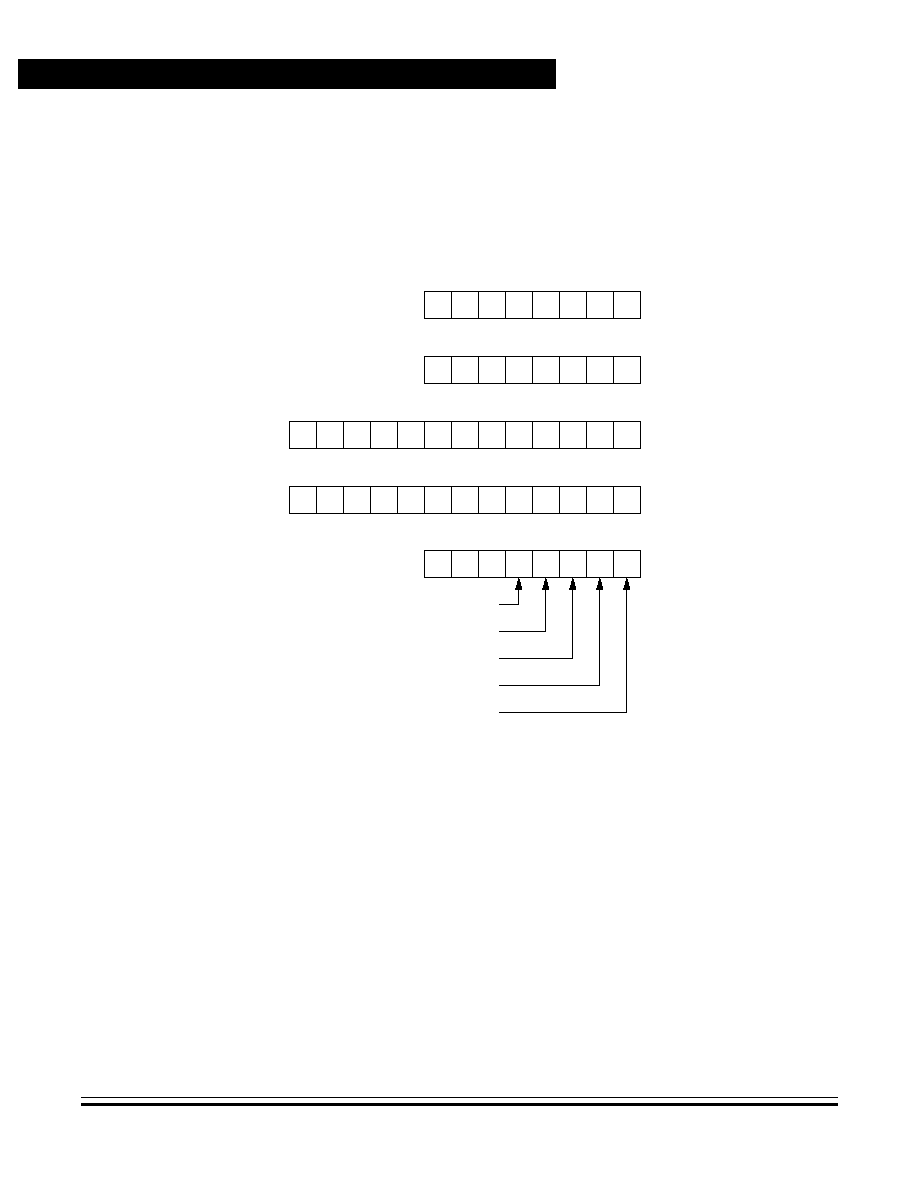
Address:
$1FDF
Bit 7
6
5
4
3
2
1
Bit 0
Read:
RAM0
RAM1
0
0
SEC
*
IRQ
0
Write:
Reset:
0
0
0
0
*
U
1
0
*
Implemented as an EPROM cell
= Unimplemented
U = Unaffected
Figure 1-1. Option Register (Option)

Technical Data
MC68HC705C8A -- Rev. 3
24
General Description
MOTOROLA
General Description
RAM0 -- Random-Access Memory Control Bit 0
1 = Maps 32 bytes of RAM into page zero starting at address
$0030. Addresses from $0020 to $002F are reserved. This bit
can be read or written at any time, allowing memory
configuration to be changed during program execution.
0 = Provides 48 bytes of PROM at location $0020≠$005F.
RAM1 -- Random-Access Memory Control Bit 1
1 = Maps 96 bytes of RAM into page one starting at address $0100.
This bit can be read or written at any time, allowing memory
configuration to be changed during program execution.
0 = Provides 96 bytes of PROM at location $0100.
SEC -- Security Bit
This bit is implemented as an erasable, programmable read-only
memory (EPROM) cell and is not affected by reset.
1 = Bootloader disabled; MCU operates only in single-chip mode
0 = Security off; bootloader can be enabled
IRQ -- Interrupt Request Pin Sensitivity Bit
IRQ is set only by reset, but can be cleared by software. This bit can
be written only once.
1 = IRQ pin is both negative edge- and level-sensitive.
0 = IRQ pin is negative edge-sensitive only.
Bits 5, 4, and 0 -- Not used; always read 0
Bit 2 -- Unaffected by reset; reads either 1 or 0
1.5 Block Diagram
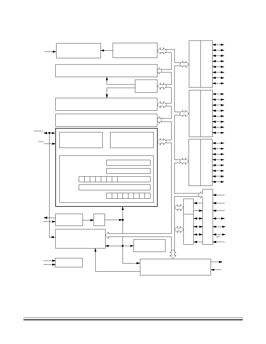
Figure 1-2
shows the structure of the MC68HC705C8A.
General Description
Block Diagram
MC68HC705C8A -- Rev. 3
Technical Data
MOTOROLA
General Description
25
Figure 1-2. MC68HC705C8A Block Diagram
INTERNAL
PROCESSOR
CLOCK
TCAP
˜
2
ACCUMULATOR
INDEX REGISTER
OSC1
OSC2
OSCILLATOR
IRQ
RESET
COP WATCHDOG
CPU
M68HC05 CPU
ARITHMETIC
V
DD
V
SS
CPU REGISTERS
CONTROL
POR
T
A
DA
TA
DIR
E
C
T
IO
N A
PA0
PA1
PA2
PA3
PA4
PA5
PA6
PA7
POWER
OPTION
EPROM/OTPROM -- 7744 BYTES
1
1
0
0
0
0
0
C
Z
N
I
H
1
1
1
16-BIT
CAPTURE/COMPARE
PO
R
T
B
D
A
TA
DI
RE
CTI
O
N
B
PB0
*
PB1
*
PB2
*
PB3
*
PB4
*
PB5
*
PB6
*
PB7
*
POR
T
C
DA
TA
DIR
E
C
T
IO
N C
PC0
PC1
PC2
PC3
PC4
PC5
PC6
PC7
TIMER SYSTEM
BAUD RATE
GENERATOR
PD7
RDI (PD0)
TDO (PD1)
MISO (PD2)
MOSI (PD3)
SCK (PD4)
SS (PD5)
SCI
SPI
TCMP
RAM -- 176 BYTES
REGISTER
BOOT ROM -- 240 BYTES
(144 BYTES CONFIGURABLE)
PROGRAM REGISTER
EPROM PROGRAMMING
V
PP
AND
CLOCK MONITOR
POR
T
D
LOGIC UNIT
(304 BYTES MAXIMUM)
CONTROL
PROGRAM COUNTER
STACK POINTER
CONDITION CODE REGISTER
* Port B pins also function as external interrupts.
PC7 has a high current sink and source capability.

Technical Data
MC68HC705C8A -- Rev. 3
26
General Description
MOTOROLA
General Description
1.6 Pin Assignments
The MC68HC705C8A is available in six packages:
∑
40-pin plastic dual in-line package (PDIP)
∑
40-pin ceramic dual in-line package (cerdip)
∑
44-lead plastic-leaded chip carrier (PLCC)
∑
44-lead ceramic-leaded chip carrier (CLCC)
∑
44-pin quad flat pack (QFP)
∑
42-pin shrink dual in-line package (SDIP)
The pin assignments for these packages are shown in
Figure 1-3
,
Figure 1-4
,
Figure 1-5
, and
Figure 1-6
.
Figure 1-3. 40-Pin PDIP/Cerdip Pin Assignments
1
2
3
4
5
6
7
8
9
10
11
12
13
14
27
28
29
30
31
32
33
34
35
36
37
38
39
40
V
DD
OSC1
OSC2
TCAP
PD7
TCMP
PD5/SS
PD4/SCK
PD3/MOSI
PD2/MISO
PD1/TDO
PD0/RDI
PC0
PC1
RESET
IRQ
V
PP
PA7
PA5
PA4
PA3
PA2
PA1
PA0
PB0
PB1
PB2
PA6
15
16
17
18
19
20
PB4
PB5
PB6
PB7
V
SS
PB3
21
22
23
24
25
26
PC2
PC3
PC4
PC5
PC6
PC7

General Description
Pin Assignments
MC68HC705C8A -- Rev. 3
Technical Data
MOTOROLA
General Description
27
Figure 1-4. 44-Lead PLCC/CLCC Pin Assignments
Figure 1-5. 44-Pin QFP Pin Assignments
PA6
PA7
V
PP
NC
IR
Q
RE
S
E
T
V
DD
OSC
1
OSC
2
TC
A
P
NC
6
5
4
3
2
1
44
43
42
41
40
39
38
37
PD7
TCMP
PD5/SS
36
35
PD4/SCK
PD3/MOSI
34
PD2/MISO
33
PD1/TDO
32
PD0/RDI
31
PC0
30
PC1
29
PC2
28
27
26
25
24
23
22
21
20
19
18
NC
PB5
PB6
PB7
V
SS
NC
PC
7
PC
6
PC
5
PC
4
PC
3
PB4
PB3
PB2
PB1
17
16
15
14
PB0
PA0
PA1
PA2
13
12
11
10
PA3
9
PA4
8
PA5
7
PD7
TCAP
OSC2
OSC1
V
DD
NC
NC
RESET
IRQ
V
PP
PA7
PA
6
PA
5
PA
4
PA
3
PA
2
PA
1
PA
0
PB0
PB1
PB2
PB3
PD
3/
M
O
SI
PD
2/
M
I
SO
PD
4/
SC
K
PD
5/
SS
TC
MP
PD
1/
T
D
O
PD
0/
R
D
I
PC
0
PC
1
PC
2
PC
3
NC
PC4
PC5
PC6
PC7
V
SS
NC
PB7
PB6
PB5
PB4
1
2
3
4
5
6
7
8
9
10 11
12
13
14
15
16
17
18
19
20
21
22
23
24
25
26
27
28
29
30
31
32
33
34
35
36
37
38
39
40
41
42
43
44

Technical Data
MC68HC705C8A -- Rev. 3
28
General Description
MOTOROLA
General Description
Figure 1-6. 42-Pin SDIP Pin Assignments
V
PP
PA7
PA6
PA5
PA4
PA3
PA2
PA1
PA0
PB0
PB1
PB2
PB3
NC
PB4
PB5
PB6
V
SS
V
DD
OSC1
OSC2
TCAP
PD7
TCMP
PD5/SS
PD4/SCK
PD3/MOSI
PD2/MISO
PD1/TDO
PD0/RDI
PC0
PC1
PC2
NC
PC3
PC4
PC5
PC6
1
2
3
4
5
6
7
8
9
10
11
12
13
14
15
16
17
18
19
20
42
41
40
39
38
37
36
35
34
33
32
31
30
29
28
27
26
25
24
23
22
PC7
PB7
21
RESET
IRQ

General Description
Pin Functions
MC68HC705C8A -- Rev. 3
Technical Data
MOTOROLA
General Description
29
1.7 Pin Functions
This subsection describes the MC68HC705C8A signals. Reference is
made, where applicable, to other sections that contain more detail about
the function being performed.
1.7.1 V
DD
and V
SS
V
DD
and V
SS
are the power supply and ground pins. The MCU operates
from a single power supply.
Very fast signal transitions occur
on the MCU pins, placing high
short-duration current demands
on the power supply. To prevent
noise problems, take special care
to provide good power supply
bypassing at the MCU. Place
bypass capacitors as close to the
MCU as possible, as shown in
Figure 1-7
.
1.7.2 V
PP
This pin provides the programming voltage to the EPROM array. For
normal operation, V
PP
shuld be tied to V
DD
.
NOTE:
Connecting the V
PP
pin (programming voltage) to V
SS
(ground) could
result in damage to the MCU.
MCU
C2
V
DD
V
SS
V+
+
C1
Figure 1-7. Bypassing Layout
Recommendation
Technical Data
MC68HC705C8A -- Rev. 3
30
General Description
MOTOROLA
General Description
1.7.3 OSC1 and OSC2
The OSC1 and OSC2 pins are the control connections for the 2-pin
on-chip oscillator. The oscillator can be driven by:
∑
Crystal resonator
∑
Ceramic resonator
∑
External clock signal
NOTE:
The frequency of the internal oscillator is f
OSC
. The MCU divides the
internal oscillator output by two to produce the internal clock with a
frequency of f
OP
.
1.7.3.1 Crystal Resonator
The circuit in
Figure 1-8
shows a
crystal oscillator circuit for an AT-cut,
parallel resonant crystal. Follow the
crystal supplier's recommendations,
because the crystal parameters
determine the external component
values required to provide reliable
startup and maximum stability. The
load capacitance values used in the
oscillator circuit design should
account for all stray layout
capacitances. To minimize output
distortion, mount the crystal and
capacitors as close as possible to the
pins.
NOTE:
Use an AT-cut crystal and not a strip or tuning fork crystal. The MCU
might overdrive or have the incorrect characteristic impedance for a strip
or tuning fork crystal.
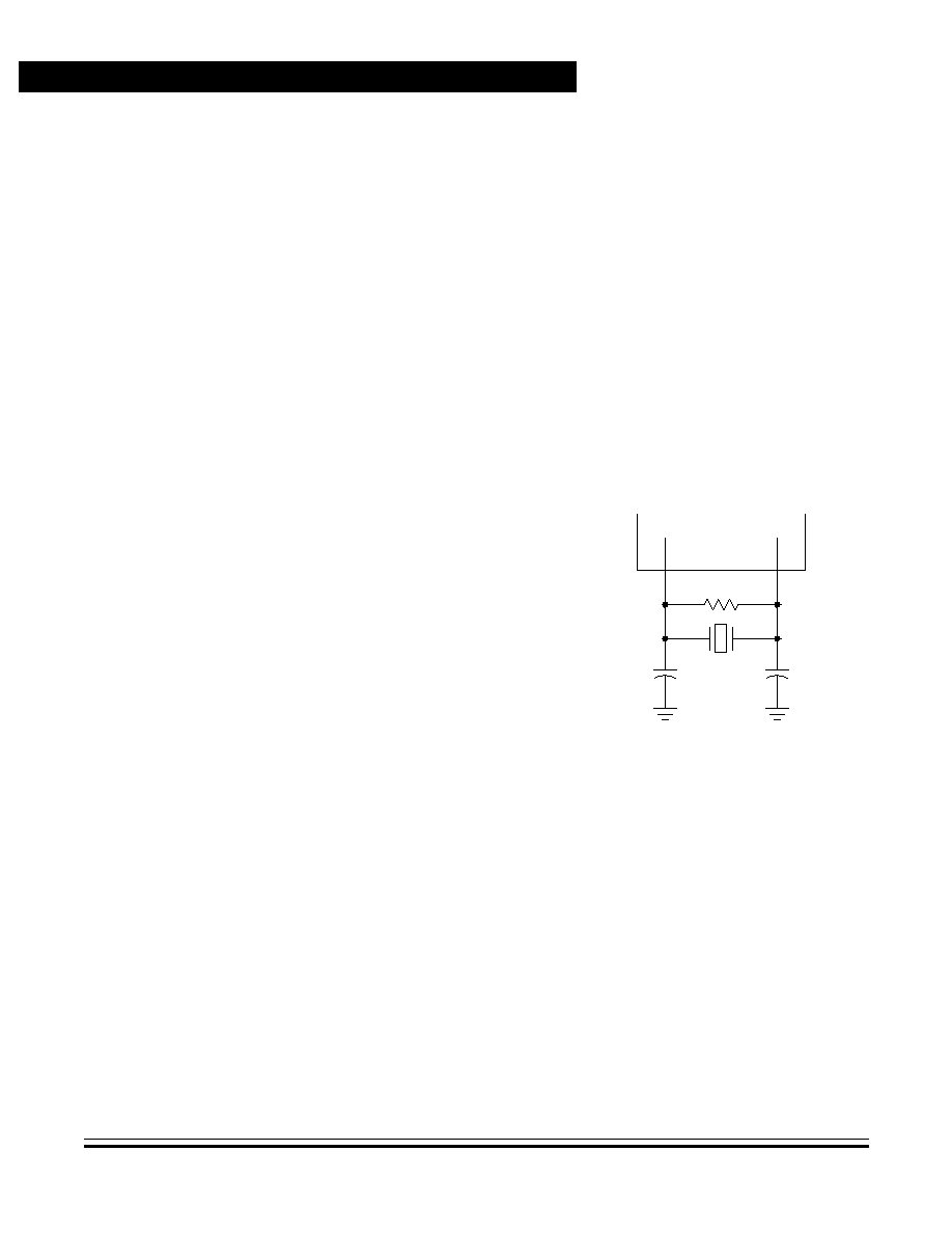
MCU
OSC1
OSC2
XTAL
22 pF
22 pF
10 M
2 MHz
Figure 1-8. Crystal
Connections
Starting value only. Follow crystal supplier's
recommendations regarding component
values that will provide reliable startup and
maximum stability.

General Description
Pin Functions
MC68HC705C8A -- Rev. 3
Technical Data
MOTOROLA
General Description
31
1.7.3.2 Ceramic Resonator
To reduce cost, use a ceramic
resonator instead of a crystal. Use the
circuit shown in
Figure 1-9
for a 2-pin
ceramic resonator or the circuit shown
in
Figure 1-10
for a 3-pin ceramic
resonator, and follow the resonator
manufacturer's recommendations.
The external component values
required for maximum stability and
reliable starting depend upon the
resonator parameters. The load
capacitance values used in the oscillator circuit design should include all
stray layout capacitances. To minimize output distortion, mount the
resonator and capacitors as close as possible to the pins.
NOTE:
The bus frequency (f
OP
) is one-half the external or crystal frequency
(f
OSC
), while the processor clock cycle (t
CYC
) is two times the f
OSC
period.
MCU
OSC1
OSC2
CERAMIC
C
C
R
RESONATOR
Figure 1-9. 2-Pin Ceramic
Resonator Connections
.
MCU
OSC1
OSC2
CERAMIC
RESONATOR
Figure 1-10. 3-Pin
Ceramic Resonator
Connections

Technical Data
MC68HC705C8A -- Rev. 3
32
General Description
MOTOROLA
General Description
1.7.3.3 External Clock Signal
An external clock from another
CMOS-compatible device can drive the
OSC1 input, with the OSC2 pin
unconnected, as
Figure 1-11
shows.
NOTE:
The bus frequency (f
OP
) is one-half the external frequency (f
OSC
) while
the processor clock cycle is two times the f
OSC
period.
1.7.4 External Reset Pin (RESET)
A logic 0 on the bidirectional RESET pin forces the MCU to a known
startup state. The RESET pin contains an internal Schmitt trigger as part
of its input to improve noise immunity. See
Section 5. Resets
.
1.7.5 External Interrupt Request Pin (IRQ)
The IRQ pin is an asynchronous external interrupt pin. The IRQ pin
contains an internal Schmitt trigger as part of its input to improve noise
immunity. See
4.3.2 External Interrupt (IRQ)
.
1.7.6 Input Capture Pin (TCAP)
The TCAP pin is the input capture pin for the on-chip capture/compare
timer. The TCAP pin contains an internal Schmitt trigger as part of its
input to improve noise immunity. See
Section 8. Capture/Compare
Timer
.
MCU
OSC
1
OS
C
2
EXTERNAL
CMOS CLOCK
Figure 1-11. External
Clock

General Description
Pin Functions
MC68HC705C8A -- Rev. 3
Technical Data
MOTOROLA
General Description
33
1.7.7 Output Compare Pin (TCMP)
The TCMP pin is the output compare pin for the on-chip
capture/compare timer. See
Section 8. Capture/Compare Timer
.
1.7.8 Port A I/O Pins (PA7≠PA0)
These eight I/O lines comprise port A, a general-purpose, bidirectional
I/O port. The pins are programmable as either inputs or outputs under
software control of the data direction registers. See
7.3 Port A
.
1.7.9 Port B I/O Pins (PB7≠PB0)
These eight I/O pins comprise port B, a general-purpose, bidirectional
I/O port. The pins are programmable as either inputs or outputs under
software control of the data direction registers. Port B pins also can be
configured to function as external interrupts. See
7.4 Port B
.
1.7.10 Port C I/O Pins (PC7≠PC0)
These eight I/O pins comprise port C, a general-purpose, bidirectional
I/O port. The pins are programmable as either inputs or outputs under
software control of the data direction registers. PC7 has a high current
sink and source capability. See
7.5 Port C
.
1.7.11 Port D I/O Pins (PD7 and PD5≠PD0)
These seven lines comprise port D, a fixed input port. All special
functions that are enabled (SPI and SCI) affect this port. See
7.6 Port D
.

Technical Data
MC68HC705C8A -- Rev. 3
34
General Description
MOTOROLA
General Description

MC68HC705C8A -- Rev. 3
Technical Data
MOTOROLA
Memory
35
Technical Data -- MC68HC705C8A
Section 2. Memory
2.1 Contents
2.2
Introduction . . . . . . . . . . . . . . . . . . . . . . . . . . . . . . . . . . . . . . . . 35
2.3
Memory Map. . . . . . . . . . . . . . . . . . . . . . . . . . . . . . . . . . . . . . . 35
2.4
Input/Output (I/O) . . . . . . . . . . . . . . . . . . . . . . . . . . . . . . . . . . . 36
2.5
RAM . . . . . . . . . . . . . . . . . . . . . . . . . . . . . . . . . . . . . . . . . . . . . 36
2.6
EPROM/OTPROM (PROM) . . . . . . . . . . . . . . . . . . . . . . . . . . . 37
2.7
Bootloader ROM . . . . . . . . . . . . . . . . . . . . . . . . . . . . . . . . . . . . 37
2.2 Introduction
This section describes the organization of the on-chip memory.
2.3 Memory Map
The central processor unit (CPU) can address eight Kbytes of memory
and input/output (I/O) registers. The program counter typically advances
one address at a time through memory, reading the program instructions
and data. The programmable read-only memory (PROM) portion of
memory -- either one-time programmable read-only memory
(OTPROM) or erasable, programmable read-only memory
(EPROM) -- holds the program instructions, fixed data, user-defined
vectors, and interrupt service routines. The random-access memory
(RAM) portion of memory holds variable data.
I/O registers are memory-mapped so that the CPU can access their
locations in the same way that it accesses all other memory locations.
The shared stack area is used during processing of an interrupt or

Technical Data
MC68HC705C8A -- Rev. 3
36
Memory
MOTOROLA
Memory
subroutine call to save the CPU state. The stack pointer decrements
during pushes and increments during pulls.
Figure 2-1
is a memory map of the MCU. Addresses $0000≠$001F,
shown in
Figure 2-2
, contain most of the control, status, and data
registers. Additional I/O registers have these addresses:
∑
$1FDF, option register
∑
$1FF0, mask option register 1 (MOR1)
∑
$1FF1, mask option register 2 (MOR2)
2.4 Input/Output (I/O)
The first 32 addresses of memory space, from $0000 to $001F, are the
I/O section. These are the addresses of the I/O control registers, status
registers, and data registers. See
Figure 2-2
for more information.
2.5 RAM
One of four selectable memory configurations is selected by the state of
the RAM1 and RAM0 bits in the option register located at $1FDF. Reset
or power-on reset (POR) clears these bits, automatically selecting the
first memory configuration as shown in
Table 2-1
. See
9.5.1 Option
Register
.
NOTE:
Be careful when using nested subroutines or multiple interrupt levels.
The CPU can overwrite data in the stack RAM during a subroutine or
during the interrupt stacking operation.
Table 2-1. Memory Configurations
RAM0
RAM1
RAM Bytes
PROM Bytes
0
0
176
7744
1
0
208
7696
0
1
272
7648
1
1
304
7600

Memory
EPROM/OTPROM (PROM)
MC68HC705C8A -- Rev. 3
Technical Data
MOTOROLA
Memory
37
2.6 EPROM/OTPROM (PROM)
An MCU with a quartz window has a maximum of 7744 bytes of EPROM.
The quartz window allows the EPROM erasure with ultraviolet light. In
an MCU without a quartz window, the EPROM cannot be erased and
serves a maximum 7744 bytes of OTPROM (see
Table 2-1
). See
Section 9. EPROM/OTPROM (PROM)
.
2.7 Bootloader ROM
The 240 bytes at addresses $1F00≠$1FEF are reserved ROM
addresses that contain the instructions for the bootloader functions. See
Section 9. EPROM/OTPROM (PROM)
.

Technical Data
MC68HC705C8A -- Rev. 3
38
Memory
MOTOROLA
Memory
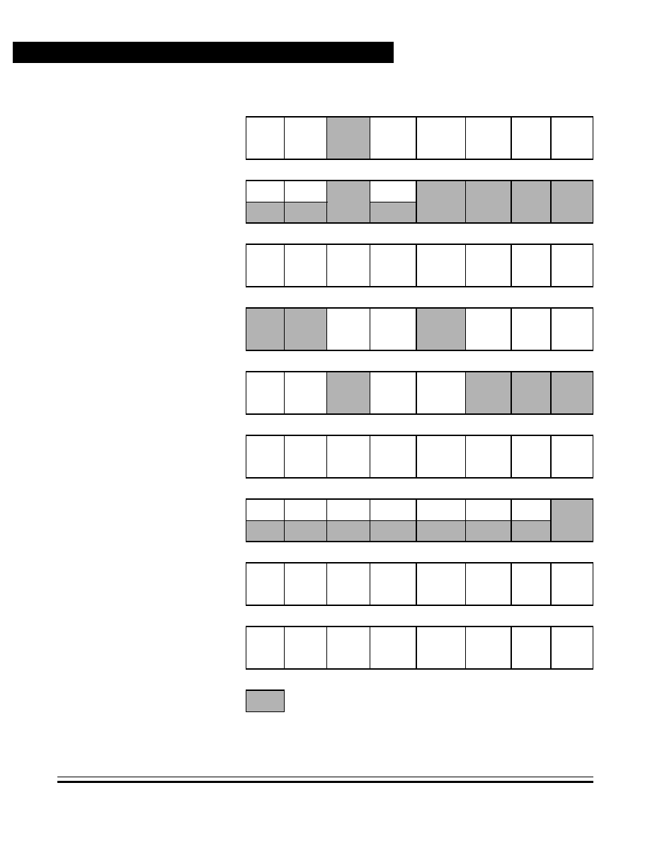
Figure 2-1. Memory Map
$0000
I/O REGISTERS
32 BYTES
PORT A DATA REGISTER
$0000
PORT B DATA REGISTER
$0001
$001F
PORT C DATA REGISTER
$0002
$0020
UNUSED
16 BYTES
USER PROM
48 BYTES
PORT D FIXED INPUT PORT
$0003
PORT A DATA DIRECTION REGISTER
$0004
$002F
PORT B DATA DIRECTION REGISTER
$0005
$0030
RAM
32 BYTES
PORT C DATA DIRECTION REGISTER
$0006
UNUSED
$0007
UNUSED
$0008
$004F
RAM0 = 1
(1)
RAM0 = 0
(1)
UNUSED
$0009
$0050
SPI CONTROL REGISTER
$000A
SPI STATUS REGISTER
$000B
$00BF
SPI DATA REGISTER
$000C
$00C0
STACK
64 BYTES
SCI BAUD RATE REGISTER
$000D
SCI CONTROL REGISTER 1
$000E
$00FF
SCI CONTROL REGISTER 2
$000F
$0100
USER PROM
96 BYTES
RAM
96 BYTES
SCI STATUS REGISTER
$0010
SCI DATA REGISTER
$0011
TIMER CONTROL REGISTER
$0012
TIMER STATUS REGISTER
$0013
INPUT CAPTURE REGISTER (HIGH)
$0014
INPUT CAPTURE REGISTER (LOW)
$0015
OUTPUT COMPARE REGISTER (HIGH)
$0016
OUTPUT COMPARE REGISTER (LOW)
$0017
$015F
RAM1 = 0
(1)
RAM1 = 1
(1)
TIMER REGISTER (HIGH)
$0018
$0160
USER PROM
7584 BYTES
TIMER REGISTER (LOW)
$0019
ALTERNATE TIMER REGISTER (HIGH)
$001A
$1EFF
ALTERNATE TIMER REGISTER (LOW)
$001B
$1F00
BOOTLOADER ROM
240 BYTES
EPROM PROGRAM REGISTER
$001C
COP RESET REGISTER
$001D
$1FDE
COP CONTROL REGISTER
$001E
$1FDF
OPTION REGISTER
UNUSED
$001F
$1FE0
$1FEF
BOOT ROM VECTORS
16 BYTES
$1FF0
MASK OPTION REGISTER 1
RESERVED
$1FF2
RESERVED
$1FF3
$1FF1
MASK OPTION REGISTER 2
SPI INTERRUPT VECTOR (HIGH)
$1FF4
SPI INTERRUPT VECTOR (LOW)
$1FF5
$1FF2
USER PROM VECTORS
12 BYTES
SCI INTERRUPT VECTOR (HIGH)
$1FF6
SCI INTERRUPT VECTOR (LOW)
$1FF7
$1FFF
TIMER INTERRUPT VECTOR (HIGH)
$1FF8
TIMER INTERRUPT VECTOR (LOW)
$1FF9
EXTERNAL INTERRUPT VECTOR (HIGH)
$1FFA
(1
)
See 9.5.1 Option Register for information.
EXTERNAL INTERRUPT VECTOR (LOW)
$1FFB
SOFTWARE INTERRUPT VECTOR (HIGH)
$1FFC
SOFTWARE INTERRUPT VECTOR (LOW)
$1FFD
RESET VECTOR (HIGH)
$1FFE
RESET VECTOR (LOW)
$1FFF
RAM
176 BYTES

Memory
Bootloader ROM
MC68HC705C8A -- Rev. 3
Technical Data
MOTOROLA
Memory
39
Addr.
Register Name
Bit 7
6
5
4
3
2
1
Bit 0
$0000
Port A Data Register
(PORTA)
See page 78.
Read:
PA7
PA6
PA5
PA4
PA3
PA2
PA1
PA0
Write:
Reset:
Unaffected by reset
$0001
Port B Data Register
(PORTB)
See page 81.
Read:
PB7
PB6
PB5
PB4
PB3
PB2
PB1
PB0
Write:
Reset:
Unaffected by reset
$0002
Port C Data Register
(PORTC)
See page 85.
Read:
PC7
PC6
PC5
PC4
PC3
PC2
PC1
PC0
Write:
Reset:
Unaffected by reset
$0003
Port D Fixed Input Register
(PORTD)
See page 88.
Read:
PD7
SS
SCK
MOSI
MISO
TDO
RDI
Write:
Reset:
Unaffected by reset
$0004
Port A Data Direction
Register (DDRA)
See page 79.
Read:
DDRA7
DDRA6
DDRA5
DDRA4
DDRA3
DDRA2
DDRA1
DDRA0
Write:
Reset:
0
0
0
0
0
0
0
0
$0005
Port B Data Direction
Register (DDRB)
See page 82.
Read:
DDRB7
DDRB6
DDRB5
DDRB4
DDRB3
DDRB2
DDRB1
DDRB0
Write:
Reset:
0
0
0
0
0
0
0
0
$0006
Port C Data Direction
(DDRC)
See page 86.
Read:
DDRC7
DDRC6
DDRC5
DDRC4
DDRC3
DDRC2
DDRC1
DDRC0
Write:
Reset:
0
0
0
0
0
0
0
0
$0007
Unimplemented
$0008
Unimplemented
$0009
Unimplemented
= Unimplemented
U = Unaffected
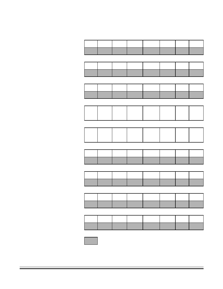
Figure 2-2. I/O Register Summary (Sheet 1 of 4)
Technical Data
MC68HC705C8A -- Rev. 3
40
Memory
MOTOROLA
Memory
$000A
SPI Control Register
(SPCR)
See page 149.
Read:
SPIE
SPE
MSTR
CPOL
CPHA
SPR1
SPR0
Write:
Reset:
0
0
0
U
U
U
U
$000B
SPI Status Register
(SPSR)
See page 151.
Read:
SPIF
WCOL
MODF
Write:
Reset:
0
0
0
$000C
SPI Data Register
(SPDR)
See page 149.
Read:
Bit 7
Bit 6
Bit 5
Bit 4
Bit 3
BIt 2
Bit 1
Bit 0
Write:
Reset:
Unaffected by reset
$000D
Baud Rate Register
(Baud)
See page 136.
Read:
SCP1
SCP0
SCR2
SCR1
SCR0
Write:
Reset:
U
U
0
0
U
U
U
U
$000E
SCI Control Register 1
(SCCR1)
See page 130.
Read:
R8
T8
M
WAKE
Write:
Reset:
U
U
U
U
$000F
SCI Control Register 2
(SCCR2)
See page 131.
Read:
TIE
TCIE
RIE
ILIE
TE
RE
RWU
SBK
Write:
Reset:
0
0
0
0
0
0
0
0
$0010
SCI Status Register
(SCSR)
See page 133.
Read: TDRE
TC
RDRF
IDLE
OR
NF
FE
Write:
Reset:
1
1
0
0
0
0
0
U
$0011
SCI Data Register
(SCDR)
See page 129.
Read:
Bit 7
Bit 6
Bit 5
Bit 4
Bit 3
Bit 2
Bit 1
Bit 0
Write:
Reset:
Unaffected by reset
$0012
Timer Control Register
(TCR)
See page 94.
Read:
ICIE
OCIE
TOIE
0
0
0
IEDG
OLVL
Write:
Reset:
0
0
0
0
0
0
U
0
Addr.
Register Name
Bit 7
6
5
4
3
2
1
Bit 0
= Unimplemented
U = Unaffected
Figure 2-2. I/O Register Summary (Sheet 2 of 4)
Memory
Bootloader ROM
MC68HC705C8A -- Rev. 3
Technical Data
MOTOROLA
Memory
41
$0013
Timer Status Register
(TSR)
See page 96.
Read:
ICF
OCF
TOF
0
0
0
0
0
Write:
Reset:
U
U
U
0
0
0
0
0
$0014
Input Capture Register
High (ICRH)
See page 100.
Read:
Bit 15
Bit 14
Bit 13
Bit 12
Bit 11
Bit 10
Bit 9
Bit 8
Write:
Reset:
Unaffected by reset
$0015
Input Capture Register
Low (ICRL)
See page 100.
Read:
Bit 7
Bit 6
Bit 5
Bit 4
Bit 3
Bit 2
Bit 1
Bit 0
Write:
Reset:
Unaffected by reset
$0016
Output Compare Register
High (OCRH)
See page 101.
Read:
Bit 15
Bit 14
Bit 13
Bit 12
Bit 11
Bit 10
Bit 9
Bit 8
Write:
Reset:
Unaffected by reset
$0017
Output Compare Register
Low (OCRL)
See page 101.
Read:
Bit 7
Bit 6
Bit 5
Bit 4
Bit 3
Bit 2
Bit 1
Bit 0
Write:
Reset:
Unaffected by reset
$0018
Timer Register High
(TRH)
See page 97.
Read:
Bit 15
Bit 14
Bit 13
Bit 12
Bit 11
Bit 10
Bit 9
Bit 8
Write:
Reset:
Reset initializes TRH to $FF
$0019
Timer Register Low
(TRL)
See page 97.
Read:
Bit 7
Bit 6
Bit 5
Bit 4
Bit 3
Bit 2
Bit 1
Bit 0
Write:
Reset:
Reset initializes TRL to $FC
$001A
Alternate Timer Register
High (ATRH)
See page 99.
Read:
Bit 15
Bit 14
Bit 13
Bit 12
Bit 11
Bit 10
Bit 9
Bit 8
Write:
Reset:
Reset initializes ATRH to $FF
$001B
Alternate Timer Register
Low (ATRL)
See page 99.
Read:
Bit 7
Bit 6
Bit 5
Bit 4
Bit 3
Bit 2
Bit 1
Bit 0
Write:
Reset:
Reset initializes ATRL to $FC
Addr.
Register Name
Bit 7
6
5
4
3
2
1
Bit 0
= Unimplemented
U = Unaffected
Figure 2-2. I/O Register Summary (Sheet 3 of 4)

Technical Data
MC68HC705C8A -- Rev. 3
42
Memory
MOTOROLA
Memory
$001C
EPROM Programming
Register (PROG)
See page 109.
Read:
0
0
0
0
0
LAT
0
PGM
Write:
Reset:
0
0
0
0
0
0
0
0
$001D
Programmable COP Reset
Register (COPRST)
See page 64.
Read:
Write:
Bit 7
Bit 6
Bit 5
Bit 4
Bit 3
Bit 2
Bit 1
Bit 0
Reset:
U
U
U
U
U
U
U
U
$001E
Programmable COP Control
Register (COPCR)
See page 64.
Read:
0
0
0
COPF
CME
PCOPE
CM1
CM0
Write:
Reset:
0
0
0
U
0
0
0
0
$001F
Unimplemented
$1FDF
Option Register
(Option)
See page 116.
Read:
RAM0
RAM1
0
0
SEC
*
IRQ
0
Write:
Reset:
0
0
0
0
*
U
1
0
*
Implemented as an EPROM cell
$1FF0
Mask Option Register 1
(MOR1)
See page 117.
Read:
PBPU7
PBPU6
PBPU5
PBPU4
PBPU3
PBPU2
PBPU1
PBPU0/
COPC
Write:
Reset:
Unaffected by reset
$1FF1
Mask Option Register 2
(MOR2)
See page 118.
Read:
NCOPE
Write:
Reset:
Unaffected by reset
Addr.
Register Name
Bit 7
6
5
4
3
2
1
Bit 0
= Unimplemented
U = Unaffected
Figure 2-2. I/O Register Summary (Sheet 4 of 4)

MC68HC705C8A -- Rev. 3
Technical Data
MOTOROLA
Central Processor Unit (CPU)
43
Technical Data -- MC68HC705C8A
Section 3. Central Processor Unit (CPU)
3.1 Contents
3.2
Introduction . . . . . . . . . . . . . . . . . . . . . . . . . . . . . . . . . . . . . . . . 43
3.3
CPU Registers . . . . . . . . . . . . . . . . . . . . . . . . . . . . . . . . . . . . . 44
3.3.1
Accumulator . . . . . . . . . . . . . . . . . . . . . . . . . . . . . . . . . . . . 45
3.3.2
Index Register . . . . . . . . . . . . . . . . . . . . . . . . . . . . . . . . . . . 45
3.3.3
Stack Pointer . . . . . . . . . . . . . . . . . . . . . . . . . . . . . . . . . . . . 46
3.3.4
Program Counter . . . . . . . . . . . . . . . . . . . . . . . . . . . . . . . . . 46
3.3.5
Condition Code Register . . . . . . . . . . . . . . . . . . . . . . . . . . . 47
3.4
Arithmetic/Logic Unit (ALU) . . . . . . . . . . . . . . . . . . . . . . . . . . . 48
3.2 Introduction
This section describes the central processor unit (CPU) registers.
Technical Data
MC68HC705C8A -- Rev. 3
44
Central Processor Unit (CPU)
MOTOROLA
Central Processor Unit (CPU)
3.3 CPU Registers
Figure 3-1
shows the five CPU registers. These are hard-wired registers
within the CPU and are not part of the memory map.
Figure 3-1. Programming Model
ACCUMULATOR (A)
INDEX REGISTER (X)
1
1
0
0
0
0
0
Z
C
I
N
1
H
1
1
Bit 0
4
Bit 7
5
CONDITION CODE REGISTER (CCR)
PROGRAM COUNTER (PC)
STACK POINTER (SP)
HALF-CARRY FLAG
INTERRUPT MASK
NEGATIVE FLAG
ZERO FLAG
CARRY/BORROW FLAG
6
3
2
1
Bit 0
4
7
5
6
3
2
1
Bit 0
4
7
5
6
3
2
1
Bit 0
4
Bit 7
5
6
3
2
1
Bit 0
4
Bit 7
5
6
3
2
1
8
Bit 12 11
10
9
8
Bit 12 11
10
9

Central Processor Unit (CPU)
CPU Registers
MC68HC705C8A -- Rev. 3
Technical Data
MOTOROLA
Central Processor Unit (CPU)
45
3.3.1 Accumulator
The accumulator (A) shown in
Figure 3-2
is a general-purpose 8-bit
register. The CPU uses the accumulator to hold operands and results of
arithmetic and non-arithmetic operations.
Figure 3-2. Accumulator (A)
3.3.2 Index Register
In the indexed addressing modes, the CPU uses the byte in the index
register (X) shown in
Figure 3-3
to determine the conditional address of
the operand. See
12.3.5 Indexed, No Offset
,
12.3.6 Indexed, 8-Bit
Offset
, and
12.3.7 Indexed, 16-Bit Offset
for more information on
indexed addressing.
The 8-bit index register also can serve as a temporary data storage
location.
Figure 3-3. Index Register (X)
Bit 7
6
5
4
3
2
1
Bit 0
Read:
Write:
Reset:
Unaffected by reset
Bit 7
6
5
4
3
2
1
Bit 0
Read:
Write:
Reset:
Unaffected by reset

Technical Data
MC68HC705C8A -- Rev. 3
46
Central Processor Unit (CPU)
MOTOROLA
Central Processor Unit (CPU)
3.3.3 Stack Pointer
The stack pointer (SP) shown in
Figure 3-4
is a 13-bit register that
contains the address of the next free location on the stack. During a reset
or after the reset stack pointer (RSP) instruction, the stack pointer
initializes to $00FF. The address in the stack pointer decrements as data
is pushed onto the stack and increments as data is pulled from the stack.
The seven most significant bits of the stack pointer are fixed
permanently at 0000011, so the stack pointer produces addresses from
$00C0 to $00FF. If subroutines and interrupts use more than 64 stack
locations, the stack pointer wraps around to address $00FF and begins
writing over the previously stored data. A subroutine uses two stack
locations. An interrupt uses five locations.
Figure 3-4. Stack Pointer (SP)
3.3.4 Program Counter
The program counter (PC) shown in
Figure 3-5
is a 13-bit register that
contains the address of the next instruction or operand to be fetched.
Normally, the address in the program counter automatically increments
to the next sequential memory location every time an instruction or
operand is fetched. Jump, branch, and interrupt operations load the
program counter with an address other than that of the next sequential
location.
Bit 12
11
10
9
8
7
6
5
4
3
2
1
Bit 0
Read:
0
0
0
0
0
1
1
Write:
Reset:
0
0
0
0
0
1
1
1
1
1
1
1
1
= Unimplemented
Bit 12
11
10
9
8
7
6
5
4
3
2
1
Bit 0
Read:
Write:
Reset:
Loaded with reset vector from $1FFE and $1FFF
Figure 3-5. Program Counter (PC)

Central Processor Unit (CPU)
CPU Registers
MC68HC705C8A -- Rev. 3
Technical Data
MOTOROLA
Central Processor Unit (CPU)
47
3.3.5 Condition Code Register
The condition code register (CCR) shown in
Figure 3-6
is an 8-bit
register whose three most significant bits are permanently fixed at 111.
The condition code register contains the interrupt mask and four bits that
indicate the results of prior instructions.
H -- Half-Carry Bit
The CPU sets the half-carry flag when a carry occurs between bits 3
and 4 of the accumulator during an add without carry (ADD) or add
with carry (ADC) operation. The half-carry bit is required for
binary-coded decimal (BCD) arithmetic operations. Reset has no
affect on the half-carry flag.
I -- Interrupt Mask Bit
Setting the interrupt mask (I) disables interrupts. If an interrupt
request occurs while the interrupt mask is a logic 0, the CPU saves
the CPU registers on the stack, sets the interrupt mask, and then
fetches the interrupt vector. If an interrupt request occurs while the
interrupt mask is set, the interrupt request is latched. The CPU
processes the latched interrupt as soon as the interrupt mask is
cleared again.
A return-from-interrupt (RTI) instruction pulls the CPU registers from
the stack, restoring the interrupt mask to its cleared state. After a
reset, the interrupt mask is set and can be cleared only by a CLI,
STOP, or WAIT instruction.
Bit 7
6
5
4
3
2
1
Bit 0
Read:
1
1
1
H
I
N
Z
C
Write:
Reset:
1
1
1
U
1
U
U
U
= Unimplemented
U = Unaffected
Figure 3-6. Condition Code Register (CCR)

Technical Data
MC68HC705C8A -- Rev. 3
48
Central Processor Unit (CPU)
MOTOROLA
Central Processor Unit (CPU)
N -- Negative Flag
The CPU sets the negative flag when an arithmetic operation, logical
operation, or data manipulation produces a negative result (bit 7 in the
results is a logic 1). Reset has no effect on the negative flag.
Z -- Zero Flag
The CPU sets the zero flag when an arithmetic operation, logical
operation, or data manipulation produces a result of $00. Reset has
no effect on the zero flag.
C -- Carry/Borrow Flag
The CPU sets the carry/borrow flag when an addition operation
produces a carry out of bit 7 of the accumulator or when a subtraction
operation requires a borrow. Some logical operations and data
manipulation instructions also clear or set the carry/borrow bit. Reset
has no effect on the carry/borrow flag.
3.4 Arithmetic/Logic Unit (ALU)
The arithmetic/logic unit (ALU) performs the arithmetic and logical
operations defined by the instruction set. The binary arithmetic circuits
decode instructions and set up the ALU for the selected operation. Most
binary arithmetic is based on the addition algorithm, carrying out
subtraction as negative addition. Multiplication is not performed as a
discrete operation but as a chain of addition and shift operations within
the ALU. The multiply instruction requires 11 internal clock cycles to
complete this chain of operations.

MC68HC705C8A -- Rev. 3
Technical Data
MOTOROLA
Interrupts
49
Technical Data -- MC68HC705C8A
Section 4. Interrupts
4.1 Contents
4.2
Introduction . . . . . . . . . . . . . . . . . . . . . . . . . . . . . . . . . . . . . . . . 49
4.3
Interrupt Sources . . . . . . . . . . . . . . . . . . . . . . . . . . . . . . . . . . . 50
4.3.1
Software Interrupt. . . . . . . . . . . . . . . . . . . . . . . . . . . . . . . . . 50
4.3.2
External Interrupt (IRQ) . . . . . . . . . . . . . . . . . . . . . . . . . . . . 51
4.3.3
Port B Interrupts . . . . . . . . . . . . . . . . . . . . . . . . . . . . . . . . . .53
4.3.4
Capture/Compare Timer Interrupts . . . . . . . . . . . . . . . . . . .55
4.3.5
SCI Interrupts . . . . . . . . . . . . . . . . . . . . . . . . . . . . . . . . . . . . 55
4.3.6
SPI Interrupts . . . . . . . . . . . . . . . . . . . . . . . . . . . . . . . . . . . . 56
4.4
Interrupt Processing . . . . . . . . . . . . . . . . . . . . . . . . . . . . . . . . .57
4.2 Introduction
This section describes how interrupts temporarily change the normal
processing sequence.

Technical Data
MC68HC705C8A -- Rev. 3
50
Interrupts
MOTOROLA
Interrupts
4.3 Interrupt Sources
These sources can generate interrupts:
∑
Software instructions (SWI)
∑
External interrupt pin (IRQ)
∑
Port B pins
∑
Serial communications interface (SCI):
≠
SCI transmit data register empty
≠
SCI transmission complete
≠
SCI receive data register full
≠
SCI receiver overrun
≠
SCI receiver input idle
∑
Serial peripheral interface (SPI):
≠
SPI transmission complete
≠
SPI mode fault
≠
SPI overrun
The IRQ pin, port B pins, SCI, and SPI can be masked (disabled) by
setting the I bit of the condition code register (CCR). The software
interrupt (SWI) instruction is non-maskable.
An interrupt temporarily changes the program sequence to process a
particular event. An interrupt does not stop the execution of the
instruction in progress but takes effect when the current instruction
completes its execution. Interrupt processing automatically saves the
central processor unit (CPU) registers on the stack and loads the
program counter with a user-defined vector address.
4.3.1 Software Interrupt
The software interrupt instruction (SWI) causes a non-maskable
interrupt.

Interrupts
Interrupt Sources
MC68HC705C8A -- Rev. 3
Technical Data
MOTOROLA
Interrupts
51
4.3.2 External Interrupt (IRQ)
An interrupt signal on the IRQ pin latches an external interrupt request.
After completing the current instruction, the CPU tests these bits:
∑
IRQ latch
∑
I bit in the CCR
Setting the I bit in the CCR disables external interrupts.
If the IRQ latch is set and the I bit is clear, the CPU then begins the
interrupt sequence. The CPU clears the IRQ latch while it fetches the
interrupt vector, so that another external interrupt request can be latched
during the interrupt service routine. As soon as the I bit is cleared during
the return-from-interrupt (RTI) instruction, the CPU can recognize the
new interrupt request.
Figure 4-1
shows the logic for external interrupts.
Figure 4-1
shows an external interrupt functional diagram.
Figure 4-2
shows an external interrupt timing diagram for the interrupt line. The
timing diagram illustrates two treatments of the interrupt line to the
processor.
1. Two single pulses on the interrupt line are spaced far enough
apart to be serviced. The minimum time between pulses is a
function of the length of the interrupt service.
Once a pulse occurs, the next pulse normally should not occur
until an RTI occurs. This time (t
ILIL
) is obtained by adding 19
instruction cycles to the total number of cycles needed to complete
the service routine (not including the RTI instruction).
2. Many interrupt lines are "wire-ORed" to the IRQ line. If the interrupt
line remains low after servicing an interrupt, then the CPU
continues to recognize an interrupt.
NOTE:
The internal interrupt latch is cleared in the first part of the interrupt
service routine. Therefore, a new external interrupt pulse could be
latched and serviced as soon as the I bit is cleared.
If the IRQ pin is not in use, connect it to the V
DD
pin.
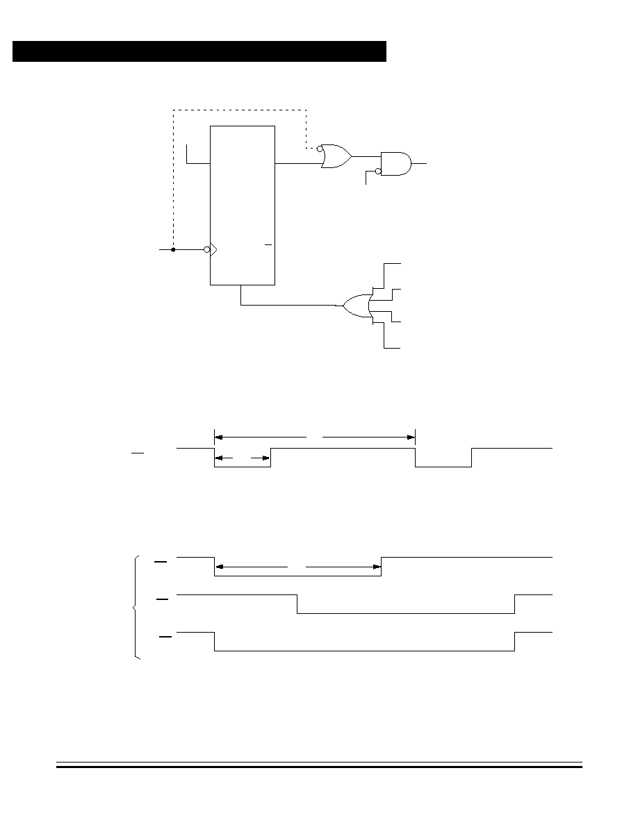
Technical Data
MC68HC705C8A -- Rev. 3
52
Interrupts
MOTOROLA
Interrupts
Figure 4-1. External Interrupt Internal Function Diagram
Figure 4-2. External Interrupt Timing
R
C
D
Q
Q
V
DD
EXTERNAL
INTERRUPT
REQUEST
I BIT (CCR)
INTERNAL RESET (COP)
EXTERNAL RESET
EXTERNAL INTERRUPT BEING SERVICED
(VECTOR FETCH)
EDGE- AND LEVEL-SENSITIVE TRIGGER
OPTION REGISTER
INTERRUPT PIN
IRQ LATCH
POR
NORMALLY
USED WITH
WIRED-OR
CONNECTION
IRQ
t
ILIH
t
ILIL
t
ILIH
IRQ PIN
IRQ
1
IRQ
n
.
.
.
a. Edge-Sensitive Trigger Condition. The minimum pulse width (t
ILIH
) is either 125 ns (f
OP
= 2.1 MHz)
or 250 ns (f
OP
= 1 MHz). The period t
ILIL
should not be less than the number of t
CYC
cycles it takes to
execute the interrupt service routine plus 19 t
CYC
cycles.
b. Level-Sensitive Trigger Condition. If the interrupt line remains low after servicing an interrupt, then the
CPU continues to recognize an interrupt.
(INTERNAL)

Interrupts
Interrupt Sources
MC68HC705C8A -- Rev. 3
Technical Data
MOTOROLA
Interrupts
53
4.3.3 Port B Interrupts
When these three conditions are true, a port B pin (PBx) acts as an
external interrupt pin:
∑
The corresponding port B pullup bit (PBPUx) in mask option
register 1 (MOR1) is programmed to a logic 1.
∑
The corresponding port B data direction bit (DDRBx) in data
direction register B (DDRB) is a logic 0.
∑
The clear interrupt mask (CLI) instruction has cleared the I bit in
the CCR.
MOR1 is an erasable, programmable read-only memory (EPROM)
register that enables the port B pullup device. Data from MOR1 is
latched on the rising edge of the voltage on the RESET pin. See
9.5.2
Mask Option Register 1
.
Port B external interrupt pins can be falling-edge sensitive only or both
falling-edge and low-level sensitive, depending on the state of the IRQ
bit in the option register at location $1FDF.
When the IRQ bit is a logic 1, a falling edge or a low level on a port B
external interrupt pin latches an external interrupt request. As long as
any port B external interrupt pin is low, an external interrupt request is
present, and the CPU continues to execute the interrupt service routine.
When the IRQ bit is a logic 0, a falling-edge only on a port B external
interrupt pin latches an external interrupt request. A subsequent port B
external interrupt request can be latched only after the voltage level of
the previous port B external interrupt signal returns to a logic 1 and then
falls again to a logic 0.
Figure 4-3
shows the port B input/output (I/O) logic.
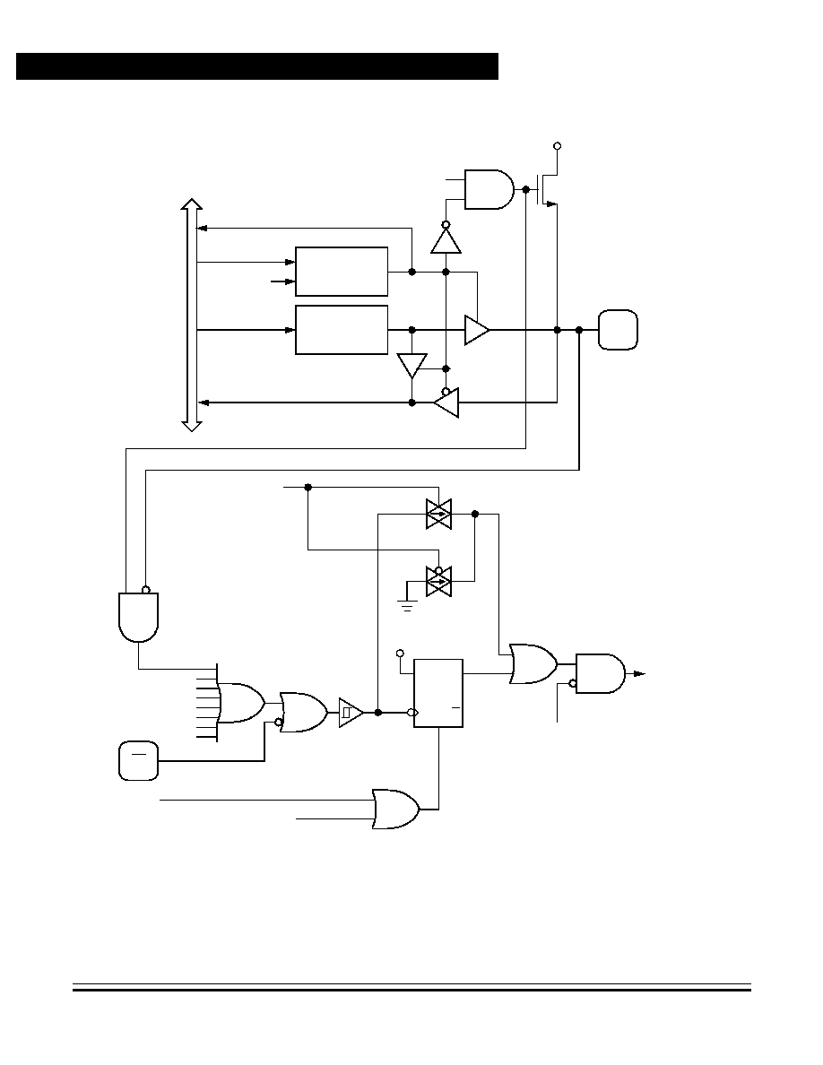
Technical Data
MC68HC705C8A -- Rev. 3
54
Interrupts
MOTOROLA
Interrupts
Figure 4-3. Port B I/O Logic
PB7
EXTERNAL
INTERRUPT
REQUEST
DATA DIRECTION
REGISTER B
BIT DDRB7
PORT B DATA
REGISTER
BIT PB7
READ $0005
WRITE $0001
READ $0001
RESET
IN
TE
RNA
L
DA
T
A
B
U
S
WRITE $0005
PBPU7
FROM OTHER
V
DD
PORT B PINS
D
C
Q
R
Q
I BIT
V
DD
FROM CCR
RESET
EXTERNAL INTERRUPT VECTOR FETCH
IRQ
IRQ
FROM OPTION
REGISTER
FROM MOR1

Interrupts
Interrupt Sources
MC68HC705C8A -- Rev. 3
Technical Data
MOTOROLA
Interrupts
55
4.3.4 Capture/Compare Timer Interrupts
Setting the I bit in the CCR disables all interrupts except for SWI.
4.3.5 SCI Interrupts
The serial communications interface (SCI) can generate these
interrupts:
∑
Transmit data register empty interrupt
∑
Transmission complete interrupt
∑
Receive data register full interrupt
∑
Receiver overrun interrupt
∑
Receiver input idle interrupt
Setting the I bit in the CCR disables all SCI interrupts.
∑
SCI Transmit Data Register Empty Interrupt -- The transmit
data register empty bit (TDRE) indicates that the SCI data register
is ready to receive a byte for transmission. TDRE becomes set
when data in the SCI data register transfers to the transmit shift
register. TDRE generates an interrupt request if the transmit
interrupt enable bit (TIE) is set also.
∑
SCI Transmission Complete Interrupt -- The transmission
complete bit (TC) indicates the completion of an SCI transmission.
TC becomes set when the TDRE bit becomes set and no data,
preamble, or break character is being transmitted. TC generates
an interrupt request if the transmission complete interrupt enable
bit (TCIE) is set also.
∑
SCI Receive Data Register Full Interrupt -- The receive data
register full bit (RDRF) indicates that a byte is ready to be read in
the SCI data register. RDRF becomes set when the data in the
receive shift register transfers to the SCI data register. RDRF
generates an interrupt request if the receive interrupt enable bit
(RIE) is set also.

Technical Data
MC68HC705C8A -- Rev. 3
56
Interrupts
MOTOROLA
Interrupts
∑
SCI Receiver Overrun Interrupt -- The overrun bit (OR)
indicates that a received byte is lost because software has not
read the previously received byte. OR becomes set when a byte
shifts into the receive shift register before software reads the word
already in the SCI data register. OR generates an interrupt
request if the receive interrupt enable bit (RIE) is set also.
∑
SCI Receiver Input Idle Interrupt -- The receiver input idle bit
(IDLE) indicates that the SCI receiver input is not receiving data.
IDLE becomes set when 10 or 11 consecutive logic 1s appear on
the receiver input. IDLE generates an interrupt request if the idle
line interrupt enable bit (ILIE) is set also.
4.3.6 SPI Interrupts
The serial peripheral interrupt (SPI) can generate these interrupts:
∑
SPI transmission complete interrupt
∑
SPI mode fault interrupt
Setting the I bit in the CCR disables all SPI interrupts.
∑
SPI Transmission Complete Interrupt -- The SPI flag bit (SPIF)
in the SPI status register indicates the completion of an SPI
transmission. SPIF becomes set when a byte shifts into or out of
the SPI data register. SPIF generates an interrupt request if the
SPIE bit is set also.
∑
SPI Mode Fault Interrupt -- The mode fault bit (MODF) in the SPI
status register indicates an SPI mode error. MODF becomes set
when a logic 0 occurs on the PD5/SS pin while the master bit
(MSTR) in the SPI control register is set. MODF generates an
interrupt request if the SPIE bit is set also.

Interrupts
Interrupt Processing
MC68HC705C8A -- Rev. 3
Technical Data
MOTOROLA
Interrupts
57
4.4 Interrupt Processing
The CPU takes these actions to begin servicing an interrupt:
1. Stores the CPU registers on the stack in the order shown in
Figure 4-4
2. Sets the I bit in the CCR to prevent further interrupts
3. Loads the program counter with the contents of the appropriate
interrupt vector locations as shown in
Table 4-1
.
The return-from-interrupt (RTI) instruction causes the CPU to recover
the CPU registers from the stack as shown in
Figure 4-4
.
Table 4-1. Reset/Interrupt Vector Addresses
Function
Source
Local
Mask
Global
Mask
Priority
(1 = Highest)
Vector Address
Reset
Power-on
logic
None
None
1
$1FFE≠$1FFF
RESET pin
Software
interrupt
(SWI)
User code
None
None
Same priority
as any
instruction
$1FFC≠$1FFD
External
interrupt
IRQ pin
None
I bit
2
$1FFA≠$1FFB
Port B pins
Timer
interrupts
ICF bit
ICIE bit
I bit
3
$1FF8≠$1FF9
OCF bit
OCIE bit
TOF bit
TOIE bit
SCI
interrupts
TDRE bit
TCIE bit
I bit
4
$1FF6≠$1FF7
TC bit
RDRF bit
RIE bit
OR bit
IDLE bit
ILIE bit
SPI
interrupts
SPIF bit
SPIE
I bit
5
$1FF4≠$1FF5
MODF bit
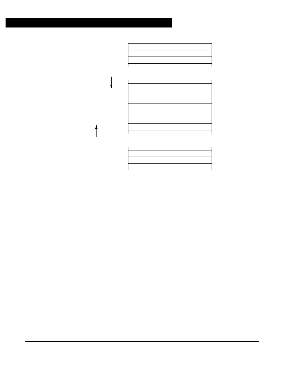
Technical Data
MC68HC705C8A -- Rev. 3
58
Interrupts
MOTOROLA
Interrupts
Figure 4-4. Interrupt Stacking Order
NOTE:
If more than one interrupt request is pending, the CPU fetches the vector
of the higher priority interrupt first. A higher priority interrupt does not
interrupt a lower priority interrupt service routine unless the lower priority
interrupt service routine clears the I bit. See
Table 4-1
for a priority
listing.
Figure 4-5
shows the sequence of events caused by an interrupt.
CONDITION CODE REGISTER
$00C0 (BOTTOM OF STACK)
$00C1
$00C2
∑
∑
∑
ACCUMULATOR
INDEX REGISTER
PROGRAM COUNTER (HIGH BYTE)
PROGRAM COUNTER (LOW BYTE)
∑
∑
∑
∑
∑
∑
∑
∑
∑
$00FD
$00FE
$00FF (TOP OF STACK)
1
2
3
4
5
5
4
3
2
1
UNSTACKING
ORDER
STACKING
ORDER
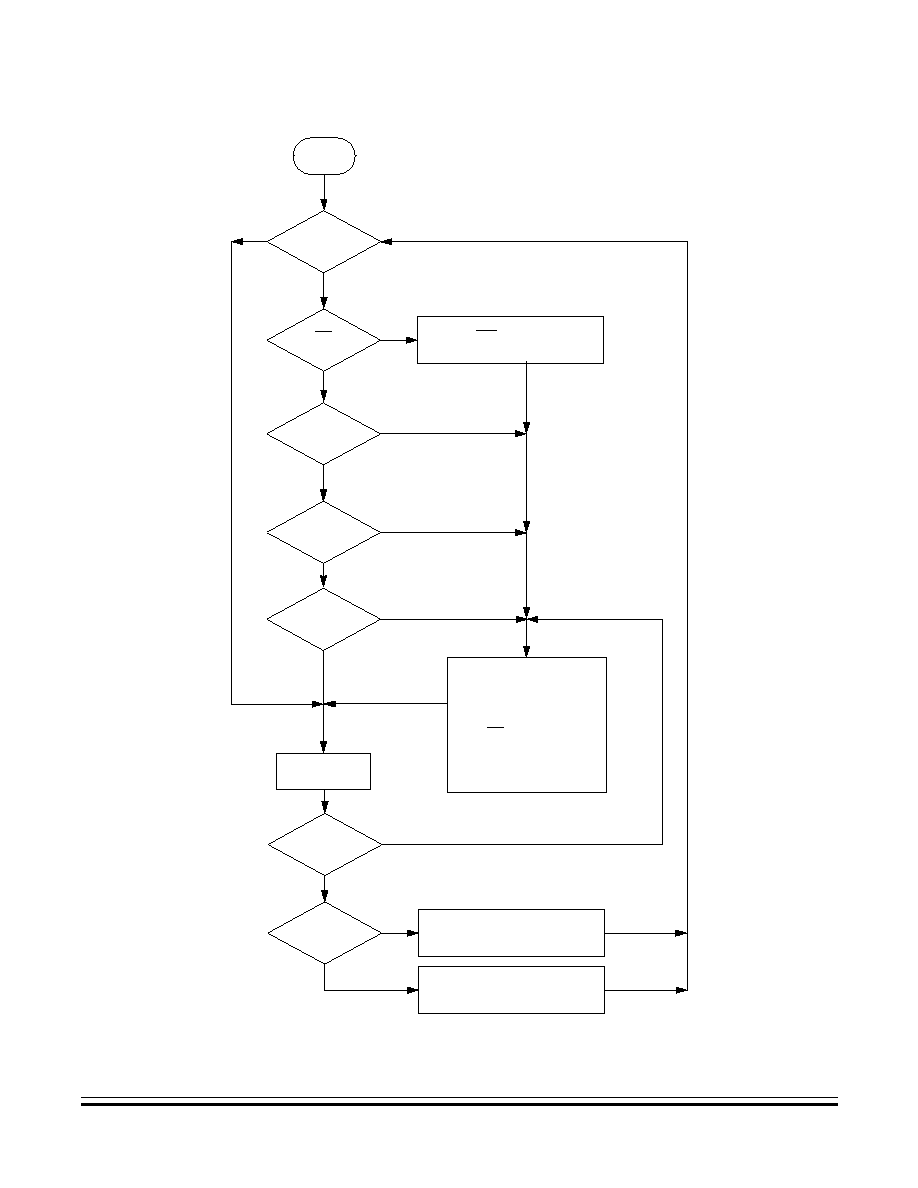
Interrupts
Interrupt Processing
MC68HC705C8A -- Rev. 3
Technical Data
MOTOROLA
Interrupts
59
Figure 4-5. Reset and Interrupt Processing Flowchart
EXTERNAL
I BIT IN
FROM
RESET
TIMER
INTERRUPT?
FETCH NEXT
INSTRUCTION
SWI
INSTRUCTION?
RTI
INSTRUCTION?
1. STACK PC, X, A, CCR
2. SET I BIT
3. LOAD PC WITH VECTOR
YES
YES
YES
YES
YES
RESTORE REGISTERS FROM STACK:
EXECUTE INSTRUCTION
CLEAR
IRQ
REQUEST LATCH
NO
NO
NO
NO
NO
SCI
INTERRUPT?
YES
YES
NO
NO
CCR REGISTER
SPI
INTERRUPT?
SWI:
IRQ:
TIMER:
SCI:
SPI:
$1FFC≠$1FFD
$1FFA≠$1FFB
$1FF8≠$1FF9
$1FF6≠$1FF7
$1FF4≠$1FF5
SET?
IRQ
INTERRUPT?
CCR, A, X, PC

Technical Data
MC68HC705C8A -- Rev. 3
60
Interrupts
MOTOROLA
Interrupts

MC68HC705C8A -- Rev. 3
Technical Data
MOTOROLA
Resets
61
Technical Data -- MC68HC705C8A
Section 5. Resets
5.1 Contents
5.2
Introduction . . . . . . . . . . . . . . . . . . . . . . . . . . . . . . . . . . . . . . . . 61
5.3
Reset Sources . . . . . . . . . . . . . . . . . . . . . . . . . . . . . . . . . . . . . 61
5.3.1
Power-On Reset (POR) . . . . . . . . . . . . . . . . . . . . . . . . . . . . 62
5.3.2
External Reset . . . . . . . . . . . . . . . . . . . . . . . . . . . . . . . . . . . 62
5.3.3
Programmable and Non-Programmable
COP Watchdog Resets . . . . . . . . . . . . . . . . . . . . . . . . . . 62
5.3.3.1
Programmable COP Watchdog Reset . . . . . . . . . . . . . . .63
5.3.3.2
Non-Programmable COP Watchdog . . . . . . . . . . . . . . . . 66
5.3.4
Clock Monitor Reset . . . . . . . . . . . . . . . . . . . . . . . . . . . . . . . 67
5.2 Introduction
This section describes how resets initialize the microcontroller unit
(MCU).
5.3 Reset Sources
A reset immediately stops the operation of the instruction being
executed, initializes certain control bits, and loads the program counter
with a user-defined reset vector address. These conditions produce a
reset:
∑
Power-on reset (POR) -- Initial power-up
∑
External reset -- A logic 0 applied to the RESET pin
∑
Internal programmable computer operating properly (COP)
watchdog timer reset
∑
Internal non-programmable COP watchdog timer reset
∑
Internal clock monitor reset

Technical Data
MC68HC705C8A -- Rev. 3
62
Resets
MOTOROLA
Resets
5.3.1 Power-On Reset (POR)
A positive transition on the V
DD
pin generates a power-on reset (POR).
The POR is strictly for the power-up condition and cannot be used to
detect drops in power supply voltage.
A 4064 t
CYC
(internal clock cycle) delay after the oscillator becomes
active allows the clock generator to stabilize. If the RESET pin is at
logic 0 at the end of 4064 t
CYC
, the MCU remains in the reset condition
until the signal on the RESET pin goes to logic 1.
5.3.2 External Reset
The minimum time required for the MCU to recognize a reset is 1 1/2
t
CYC
.
However, to guarantee that the MCU recognizes an external reset
as an external reset and not as a COP or clock monitor reset, the RESET
pin must be low for eight t
CYC
. After six t
CYC
, the input on the RESET pin
is sampled. If the pin is still low, an external reset has occurred. If the
input is high, then the MCU assumes that the reset was initiated
internally by either the COP watchdog timer or by the clock monitor. This
method of differentiating between external and internal reset conditions
assumes that the RESET pin will rise to a logic 1 less than two t
CYC
after
its release and that an externally generated reset should stay active for
at least eight t
CYC
.
5.3.3 Programmable and Non-Programmable COP Watchdog Resets
A timeout of a COP watchdog generates a COP reset. A COP watchdog,
once enabled, is part of a software error detection system and must be
cleared periodically to start a new timeout period.
The MC68HC705C8A has two different COP watchdogs for compatibility
with devices such as the MC68HC705C8 and the MC68HC05C4A:
1. Programmable COP watchdog reset
2. Non-programmable COP watchdog
One COP has four programmable timeout periods and the other has a
fixed non-programmable timeout period.

Resets
Reset Sources
MC68HC705C8A -- Rev. 3
Technical Data
MOTOROLA
Resets
63
5.3.3.1 Programmable COP Watchdog Reset
A timeout of the 18-stage ripple counter in the programmable COP
watchdog generates a reset.
Figure 5-1
is a diagram of the
programmable COP watchdog. Two registers control and monitor
operation of the programmable COP watchdog:
∑
COP reset register (COPRST), $001D
∑
COP control register (COPCR), $001E
To clear the programmable COP watchdog and begin a new timeout
period, write these values to the COP reset register (COPRST).
See
Figure 5-2
.
1. $55
2. $AA
The $55 write must precede the $AA write. Instructions may be executed
between the write operations provided that the COP watchdog does not
time out before the second write.
Figure 5-1. Programmable COP Watchdog Diagram
˜
2
˜
2
˜
2
˜
2
˜
2
˜
2
˜
2
˜
2
˜
2
˜
2
˜
2
˜
2
˜
2
˜
2
˜
2
˜
4
˜
4
˜
2
˜
2
˜
2
˜
2
˜
2
˜
2
2
21
2
19
2
17
2
13
2
15
CM1
CM0
COPRST
PCOPE
RESET
INTERNAL
CLOCK
(f
OP
)
PROGRAMMABLE COP WATCHDOG (MC68HC705C8 TYPE)
˜
2
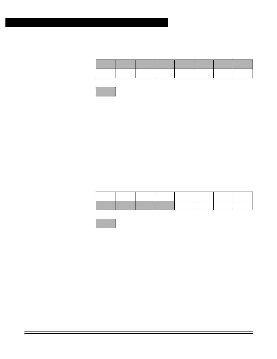
Technical Data
MC68HC705C8A -- Rev. 3
64
Resets
MOTOROLA
Resets
The programmable COP control register (COPCR) shown in
Figure 5-3
does these functions:
∑
Flags programmable COP watchdog resets
∑
Enables the clock monitor
∑
Enables the programmable COP watchdog
∑
Controls the timeout period of the programmable COP watchdog
COPF -- COP Flag
This read-only bit is set when a timeout of the programmable COP
watchdog occurs or when the clock monitor detects a slow or absent
internal clock. Clear the COPF bit by reading the COP control register.
Reset has no effect on the COPF bit.
1 = COP timeout or internal clock failure
0 = No COP timeout and no internal clock failure
Address:
$001D
Bit 7
6
5
4
3
2
1
Bit 0
Read:
Write:
Bit 7
6
5
4
3
2
1
Bit 0
Reset:
U
U
U
U
U
U
U
U
= Unimplemented
U = Unaffected
Figure 5-2. Programmable COP Reset Register (COPRST)
Address:
$001E
Bit 7
6
5
4
3
2
1
Bit 0
Read:
0
0
0
COPF
CME
PCOPE
CM1
CM0
Write:
Reset:
0
0
0
U
0
0
0
0
= Unimplemented
U = Unaffected
Figure 5-3. Programmable COP Control Register (COPCR)

Resets
Reset Sources
MC68HC705C8A -- Rev. 3
Technical Data
MOTOROLA
Resets
65
CME -- Clock Monitor Enable Bit
This read/write bit enables the clock monitor. The clock monitor sets
the COPF bit and generates a reset if it detects an absent internal
clock for a period of from 5
µ
s to 100
µ
s. CME is readable and writable
at any time. Reset clears the CME bit.
1 = Clock monitor enabled
0 = Clock monitor disabled
NOTE:
Do not enable the clock monitor in applications with an internal clock
frequency of 200 kHz or less.
If the clock monitor detects a slow clock, it drives the bidirectional
RESET pin low for four clock cycles. If the clock monitor detects an
absent clock, it drives the RESET pin low until the clock recovers.
PCOPE -- Programmable COP Enable Bit
This read/write bit enables the programmable COP watchdog.
PCOPE is readable at any time but can be written only once after
reset. Reset clears the PCOPE bit.
1 = Programmable COP watchdog enabled
0 = Programmable COP watchdog disabled
NOTE:
Programming the non-programmable COP enable bit (NCOPE) in mask
option register 2 (MOR2) to logic 1 enables the non-programmable COP
watchdog. Setting the PCOPE bit while the NCOPE bit is programmed
to logic 1 enables both COP watchdogs to operate at the same time.
(See
9.5.3 Mask Option Register 2
.)
CM1 and CM0 -- COP Mode Bits
These read/write bits select the timeout period of the programmable
COP watchdog. (See
Table 5-1
.) CM1 and CM0 can be read anytime
but can be written only once. They can be cleared only by reset.
Bits 7≠5 -- Unused
Bits 7≠5 always read as logic 0s. Reset clears bits 7≠5.

Technical Data
MC68HC705C8A -- Rev. 3
66
Resets
MOTOROLA
Resets
5.3.3.2 Non-Programmable COP Watchdog
A timeout of the 18-stage ripple counter in the non-programmable COP
watchdog generates a reset. The timeout period is 65.536 ms when
f
OSC
= 4 MHz. The timeout period for the non-programmable COP timer
is a direct function of the crystal frequency. The equation is:
Two memory locations control operation of the non-programmable COP
watchdog:
1. Non-programmable COP enable bit (NCOPE) in mask option
register 2 (MOR2)
Programming the NCOPE bit in MOR2 to a logic 1 enables the
non-programmable COP watchdog. See
9.5.3 Mask Option
Register 2
.
NOTE:
Writing a logic 1 to the programmable COP enable bit (PCOPE) in the
COP control register enables the programmable COP watchdog. Setting
the PCOPE bit while the NCOPE bit is programmed to logic 1 enables
both COP watchdogs to operate at the same time.
Table 5-1. Programmable COP Timeout Period Selection
CM1:CM0
COP
Timeout Rate
Programmable COP Timeout Period
f
OSC
= 4.0 MHz
f
OP
= 2.0 MHz
f
OSC
= 3.5795 MHz
f
OP
= 1.7897 MHz
f
OSC
= 2.0 MHz
f
OP
= 1.0 MHz
f
OSC
= 1.0 MHz
f
OP
= 0.5 MHz
00
f
OP
˜
2
15
16.38 ms
18.31 ms
32.77 ms
65.54 ms
01
f
OP
˜
2
17
65.54 ms
73.24 ms
131.07 ms
262.14 ms
10
f
OP
˜
2
19
262.14 ms
292.95 ms
524.29 ms
1.048 s
11
f
OP
˜
2
21
1.048 s
1.172 s
2.097 s
4.194 s
262,144
f
OSC
Timeout period =

Resets
Reset Sources
MC68HC705C8A -- Rev. 3
Technical Data
MOTOROLA
Resets
67
2. COP clear bit (COPC) at address $1FF0
To clear the non-programmable COP watchdog and start a new
COP timeout period, write a logic 0 to bit 0 of address $1FF0.
Reading address $1FF0 returns the mask option register 1
(MOR1) data at that location. See
9.5.2 Mask Option Register 1
.
NOTE:
The non-programmable watchdog COP is disabled in bootloader mode,
even if the NCOPE bit is programmed.
Figure 5-4
is a diagram of the non-programmable COP.
Figure 5-4. Non-Programmable COP Watchdog Diagram
5.3.4 Clock Monitor Reset
When the CME bit in the COP control register is set, the clock monitor
detects the absence of the internal bus clock for a certain period of time.
The timeout period depends on processing parameters and varies from
5
µ
s to 100
µ
s, which implies that systems using a bus clock rate of
200 kHz or less should not use the clock monitor function.
If a slow or absent clock is detected, the clock monitor causes a system
reset. The reset is issued to the external system for four bus cycles using
the bidirectional RESET pin.
Special consideration is required when using the STOP instruction with
the clock monitor. Since STOP causes the system clocks to halt, the
clock monitor issues a system reset when STOP is executed.
˜
2
˜
2
˜
2
˜
2
˜
2
˜
2
˜
2
˜
2
˜
2
˜
2
˜
2
˜
2
˜
2
˜
2
˜
2
˜
2
˜
2
NCOPE
NON-PROGRAMMABLE COP WATCHDOG (MC68HC05C4A TYPE)

Technical Data
MC68HC705C8A -- Rev. 3
68
Resets
MOTOROLA
Resets
The clock monitor is a useful backup to the COP watchdog system.
Because the watchdog timer requires a clock to function, it cannot
indicate a system clock failure. The clock monitor would detect such a
condition and force the MCU to a reset state. Clocks are not required for
the MCU to reach a reset condition. They are, however, required to bring
the MCU through the reset sequence and back to run condition.

MC68HC705C8A -- Rev. 3
Technical Data
MOTOROLA
Low-Power Modes
69
Technical Data -- MC68HC705C8A
Section 6. Low-Power Modes
6.1 Contents
6.2
Introduction . . . . . . . . . . . . . . . . . . . . . . . . . . . . . . . . . . . . . . . . 69
6.3
Stop Mode . . . . . . . . . . . . . . . . . . . . . . . . . . . . . . . . . . . . . . . . 69
6.3.1
SCI During Stop Mode . . . . . . . . . . . . . . . . . . . . . . . . . . . . .71
6.3.2
SPI During Stop Mode . . . . . . . . . . . . . . . . . . . . . . . . . . . . . 71
6.3.3
Programmable COP Watchdog in Stop Mode . . . . . . . . . . . 71
6.3.4
Non-Programmable COP Watchdog in Stop Mode . . . . . . . 73
6.4
Wait Mode. . . . . . . . . . . . . . . . . . . . . . . . . . . . . . . . . . . . . . . . . 73
6.4.1
Programmable COP Watchdog in Wait Mode . . . . . . . . . . . 75
6.4.2
Non-Programmable COP Watchdog in Wait Mode . . . . . . . 75
6.5
Data-Retention Mode . . . . . . . . . . . . . . . . . . . . . . . . . . . . . . . . 75
6.2 Introduction
This section describes the three low-power modes:
∑
Stop mode
∑
Wait mode
∑
Data-retention mode
6.3 Stop Mode
The STOP instruction places the microcontroller unit (MCU) in its lowest
power consumption mode. In stop mode, the internal oscillator is turned
off, halting all internal processing including timer, serial communications
interface (SCI), and master mode serial peripheral interface (SPI)
operation. See
Figure 6-1
.
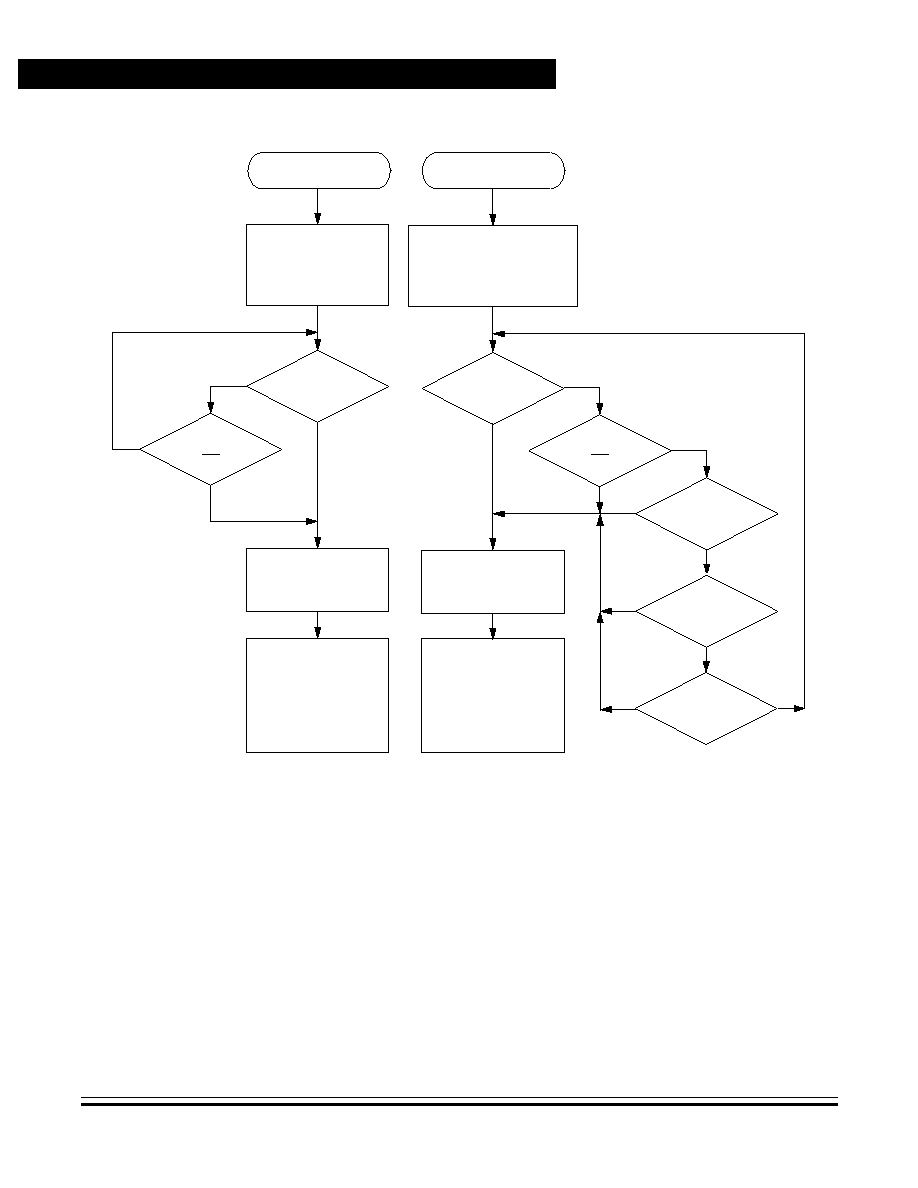
Technical Data
MC68HC705C8A -- Rev. 3
70
Low-Power Modes
MOTOROLA
Low-Power Modes
Figure 6-1. Stop/Wait Mode Function Flowchart
During stop mode, the I bit in the condition code register (CCR) is
cleared to enable external interrupts. All other registers and memory
remain unaltered. All input/output (I/O) lines remain unchanged. The
processor can be brought out of stop mode only by an external interrupt
or reset.
NO
YES
YES
YES
YES
YES
NO
NO
NO
NO
YES
NO
NO
YES
STOP
RESET
EXTERNAL
INTERRUPT
(IRQ)
TURN ON OSCILLATOR
WAIT FOR TIME
DELAY TO STABILIZE
1. FETCH RESET VECTOR
2. SERVICE INTERRUPT:
a. STACK
b. SET I BIT
c. VECTOR TO
INTERRUPT ROUTINE
STOP OSCILLATOR
AND ALL CLOCKS
CLEAR I BIT
WAIT
OSCILLATOR ACTIVE
TIMER, SCI, AND SPI
CLOCKS ACTIVE
CPU CLOCKS STOPPED
RESET
EXTERNAL
INTERRUPT
(IRQ)
INTERNAL TIMER
INTERRUPT
INTERNAL SCI
INTERRUPT
INTERNAL SPI
INTERRUPT
RESTART CPU CLOCK
1. FETCH RESET VECTOR
2. SERVICE INTERRUPT:
a. STACK
b. SET I BIT
c. VECTOR TO
INTERRUPT ROUTINE
CLEAR I BIT
OR
OR

Low-Power Modes
Stop Mode
MC68HC705C8A -- Rev. 3
Technical Data
MOTOROLA
Low-Power Modes
71
6.3.1 SCI During Stop Mode
When the MCU enters stop mode, the baud rate generator stops, halting
all SCI activity. If the STOP instruction is executed during a transmitter
transfer, that transfer is halted. If a low input to the IRQ pin is used to exit
stop mode, the transfer resumes.
If the SCI receiver is receiving data and stop mode is entered, received
data sampling stops because the baud rate generator stops, and all
subsequent data is lost. Therefore, all SCI transfers should be in the idle
state when the STOP instruction is executed.
6.3.2 SPI During Stop Mode
When the MCU enters stop mode, the baud rate generator stops,
terminating all master mode SPI operations. If the STOP instruction is
executed during an SPI transfer, that transfer halts until the MCU exits
stop mode by a low signal on the IRQ pin. If reset is used to exit stop
mode, the SPI control and status bits are cleared, and the SPI is
disabled.
If the MCU is in slave mode when the STOP instruction is executed, the
slave SPI continues to operate and can still accept data and clock
information in addition to transmitting its own data back to a master
device. At the end of a possible transmission with a slave SPI in stop
mode, no flags are set until a low on the IRQ pin wakes up the MCU.
NOTE:
Although a slave SPI in stop mode can exchange data with a master SPI,
the status bits of a slave SPI are inactive in stop mode.
6.3.3 Programmable COP Watchdog in Stop Mode
The STOP instruction turns off the internal oscillator and suspends the
computer operating properly (COP) watchdog counter. If the RESET pin
brings the MCU out of stop mode, the reset function clears and disables
the COP watchdog.
If the IRQ pin brings the MCU out of stop mode, the COP counter
resumes counting from its suspended value after the 4064-t
CYC
clock
stabilization delay. See
Figure 6-2
.

Technical Data
MC68HC705C8A -- Rev. 3
72
Low-Power Modes
MOTOROLA
Low-Power Modes
NOTE:
If the clock monitor is enabled (CME = 1), the STOP instruction causes
the clock monitor to time out and reset the MCU.
Figure 6-2. Programmable COP Watchdog
in Stop Mode (PCOPE = 1) Flowchart
STABILIZATION
STOP
EXTERNAL
RESET?
NO
NO
TURN ON INTERNAL OSCILLATOR
YES
YES
END OF
DELAY?
YES
NO
1. LOAD PC WITH RESET VECTOR
OR
2. SERVICE INTERRUPT:
a. SAVE CPU REGISTERS ON STACK
b. SET I BIT IN CCR
c. LOAD PC WITH INTERRUPT VECTOR
CLEAR I BIT IN CCR
TURN OFF INTERNAL OSCILLATOR
TURN ON INTERNAL CLOCK
SUSPEND COP COUNTER
TURN ON INTERNAL OSCILLATOR
END OF
STABILIZATION
DELAY?
YES
NO
1. LOAD PC WITH RESET VECTOR
OR
2. SERVICE INTERRUPT:
a. SAVE CPU REGISTERS ON STACK
b. SET I BIT IN CCR
c. LOAD PC WITH INTERRUPT VECTOR
TURN ON INTERNAL CLOCK
CLEAR COP COUNTER
CLEAR PCOPE BIT IN COPCR
RESUME COP WATCHDOG COUNT
EXTERNAL
INTERRUPT?

Low-Power Modes
Wait Mode
MC68HC705C8A -- Rev. 3
Technical Data
MOTOROLA
Low-Power Modes
73
6.3.4 Non-Programmable COP Watchdog in Stop Mode
The STOP instruction has these effects on the non-programmable COP
watchdog:
∑
Turns off the oscillator and the COP watchdog counter
∑
Clears the COP watchdog counter
If the RESET pin brings the MCU out of stop mode, the COP watchdog
begins counting immediately. The reset function clears the COP counter
again after the 4064-t
CYC
clock stabilization delay.
If the IRQ pin brings the MCU out of stop mode, the COP watchdog
begins counting immediately. The IRQ function does not clear the
COP counter again after the 4064-t
CYC
clock stabilization delay. See
Figure 6-3
.
NOTE:
If the clock monitor is enabled (CME = 1), the STOP instruction causes
it to time out and reset the MCU.
6.4 Wait Mode
The WAIT instruction places the MCU in an intermediate power
consumption mode. All central processor unit (CPU) activity is
suspended, but the oscillator, capture/compare timer, SCI, and SPI
remain active. Any interrupt or reset brings the MCU out of wait mode.
See
Figure 6-1
.
The WAIT instruction has these effects on the CPU:
∑
Clears the I bit in the condition code register, enabling interrupts
∑
Stops the CPU clock, but allows the internal clock to drive the
capture/compare timer, SCI, and SPI
The WAIT instruction does not affect any other registers or I/O lines. The
capture/compare timer, SCI, and SPI can be enabled to allow a periodic
exit from wait mode.
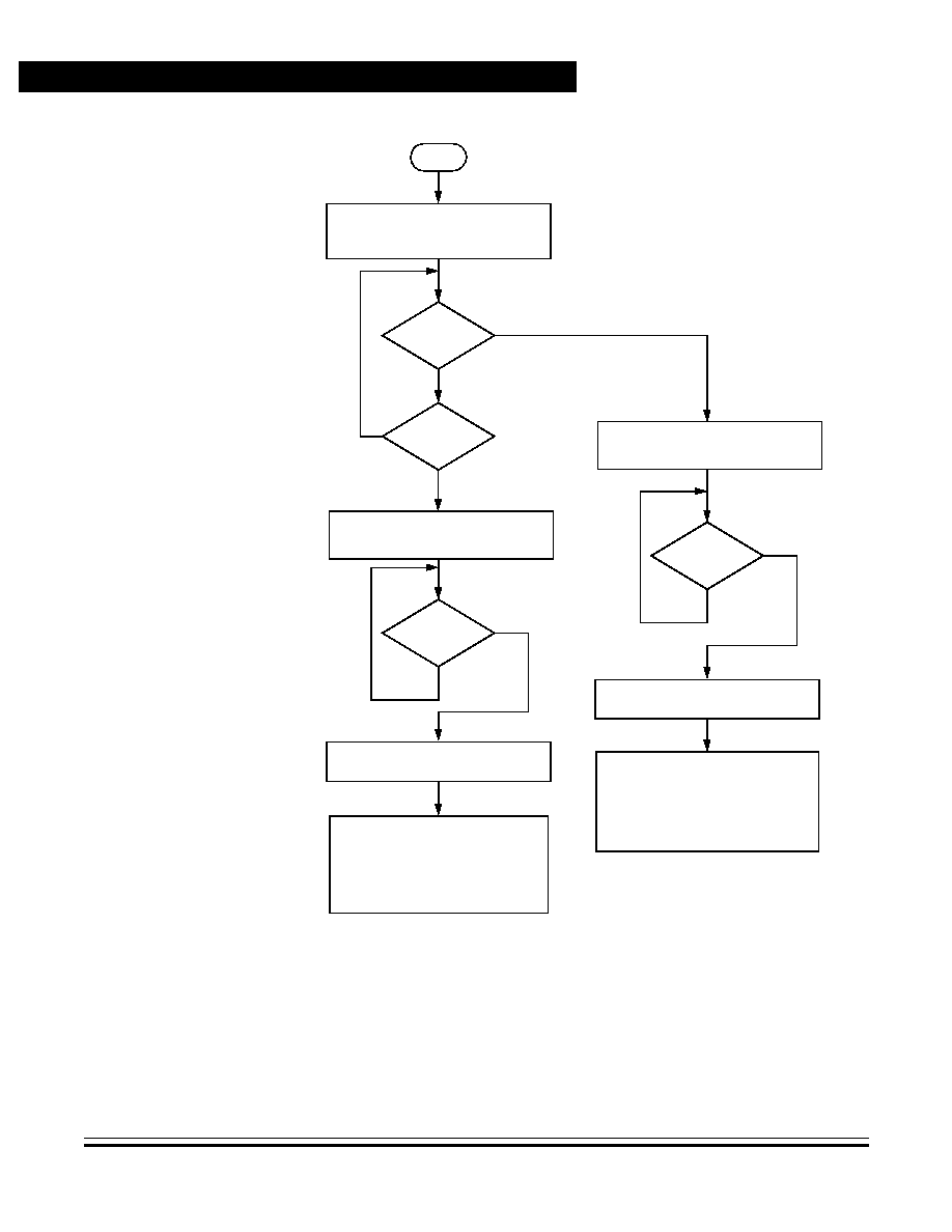
Technical Data
MC68HC705C8A -- Rev. 3
74
Low-Power Modes
MOTOROLA
Low-Power Modes
Figure 6-3. Non-Programmable COP Watchdog
in Stop Mode (NCOPE = 1) Flowchart
STABILIZATION
STOP
EXTERNAL
RESET?
NO
NO
TURN ON INTERNAL OSCILLATOR
YES
YES
END OF
DELAY?
YES
NO
1. LOAD PC WITH RESET VECTOR
OR
2. SERVICE INTERRUPT:
a. SAVE CPU REGISTERS ON STACK
b. SET I BIT IN CCR
c. LOAD PC WITH INTERRUPT VECTOR
CLEAR I BIT IN CCR
CLEAR COP COUNTER
TURN ON INTERNAL CLOCK
TURN OFF INTERNAL OSCILLATOR
TURN ON INTERNAL OSCILLATOR
END OF
STABILIZATION
DELAY?
YES
NO
1. LOAD PC WITH RESET VECTOR
OR
2. SERVICE INTERRUPT:
a. SAVE CPU REGISTERS ON STACK
b. SET I BIT IN CCR
c. LOAD PC WITH INTERRUPT VECTOR
CLEAR COP COUNTER
TURN ON COP WATCHDOG
EXTERNAL
INTERRUPT?
TURN OFF COP COUNTER
TURN ON COP WATCHDOG
TURN ON INTERNAL CLOCK

Low-Power Modes
Data-Retention Mode
MC68HC705C8A -- Rev. 3
Technical Data
MOTOROLA
Low-Power Modes
75
6.4.1 Programmable COP Watchdog in Wait Mode
The programmable COP watchdog is active during wait mode. Software
must periodically bring the MCU out of wait mode to clear the
programmable COP watchdog.
6.4.2 Non-Programmable COP Watchdog in Wait Mode
The non-programmable COP watchdog is active during wait mode.
Software must periodically bring the MCU out of wait mode to clear the
non-programmable COP watchdog.
6.5 Data-Retention Mode
In data-retention mode, the MCU retains random-access memory (RAM)
contents and CPU register contents at V
DD
voltages as low as 2.0 Vdc.
The data-retention feature allows the MCU to remain in a low
power-consumption state during which it retains data, but the CPU
cannot execute instructions.
To put the MCU in data-retention mode:
1. Drive the RESET pin to logic 0.
2. Lower V
DD
voltage. The RESET pin must remain low continuously
during data-retention mode.
To take the MCU out of data-retention mode:
1. Return V
DD
to normal operating voltage.
2. Return the RESET pin to logic 1.

Technical Data
MC68HC705C8A -- Rev. 3
76
Low-Power Modes
MOTOROLA
Low-Power Modes

MC68HC705C8A -- Rev. 3
Technical Data
MOTOROLA
Parallel Input/Output (I/O)
77
Technical Data -- MC68HC705C8A
Section 7. Parallel Input/Output (I/O)
7.1 Contents
7.2
Introduction . . . . . . . . . . . . . . . . . . . . . . . . . . . . . . . . . . . . . . . . 77
7.3
Port A . . . . . . . . . . . . . . . . . . . . . . . . . . . . . . . . . . . . . . . . . . . . 78
7.3.1
Port A Data Register . . . . . . . . . . . . . . . . . . . . . . . . . . . . . . 78
7.3.2
Data Direction Register A . . . . . . . . . . . . . . . . . . . . . . . . . . . 79
7.3.3
Port A Logic . . . . . . . . . . . . . . . . . . . . . . . . . . . . . . . . . . . . . 80
7.4
Port B . . . . . . . . . . . . . . . . . . . . . . . . . . . . . . . . . . . . . . . . . . . . 81
7.4.1
Port B Data Register . . . . . . . . . . . . . . . . . . . . . . . . . . . . . . 81
7.4.2
Data Direction Register B . . . . . . . . . . . . . . . . . . . . . . . . . . . 82
7.4.3
Port B Logic . . . . . . . . . . . . . . . . . . . . . . . . . . . . . . . . . . . . . 83
7.5
Port C . . . . . . . . . . . . . . . . . . . . . . . . . . . . . . . . . . . . . . . . . . . . 85
7.5.1
Port C Data Register . . . . . . . . . . . . . . . . . . . . . . . . . . . . . . 85
7.5.2
Data Direction Register C. . . . . . . . . . . . . . . . . . . . . . . . . . . 86
7.5.3
Port C Logic . . . . . . . . . . . . . . . . . . . . . . . . . . . . . . . . . . . . . 87
7.6
Port D . . . . . . . . . . . . . . . . . . . . . . . . . . . . . . . . . . . . . . . . . . . . 88
7.2 Introduction
This section describes the programming of ports A, B, C, and D.
Technical Data
MC68HC705C8A -- Rev. 3
78
Parallel Input/Output (I/O)
MOTOROLA
Parallel Input/Output (I/O)
7.3 Port A
Port A is an 8-bit, general-purpose, bidirectional input/output (I/O) port.
7.3.1 Port A Data Register
The port A data register (PORTA) shown in
Figure 7-1
contains a data
latch for each of the eight port A pins. When a port A pin is programmed
to be an output, the state of its data register bit determines the state of
the output pin. When a port A pin is programmed to be an input, reading
the port A data register returns the logic state of the pin.
PA7≠PA0 -- Port A Data Bits
These read/write bits are software programmable. Data direction of
each bit is under the control of the corresponding bit in data direction
register A. Reset has no effect on port A data.
Address:
$0000
Bit 7
6
5
4
3
2
1
Bit 0
Read:
PA7
PA6
PA5
PA4
PA3
PA2
PA1
PA0
Write:
Reset:
Unaffected by reset
Figure 7-1. Port A Data Register (PORTA)

Parallel Input/Output (I/O)
Port A
MC68HC705C8A -- Rev. 3
Technical Data
MOTOROLA
Parallel Input/Output (I/O)
79
7.3.2 Data Direction Register A
The contents of data direction register A (DDRA) shown in
Figure 7-2
determine whether each port A pin is an input or an output. Writing a
logic 1 to a DDRA bit enables the output buffer for the associated port A
pin; a logic 0 disables the output buffer. A reset clears all DDRA bits,
configuring all port A pins as inputs.
DDRA7≠DDRA0 -- Port A Data Direction Bits
These read/write bits control port A data direction. Reset clears bits
DDRA7≠DDRA0.
1 = Corresponding port A pin configured as output
0 = Corresponding port A pin configured as input
NOTE:
Avoid glitches on port A pins by writing to the port A data register before
changing DDRA bits from logic 0 to logic 1.
Address:
$0004
Bit 7
6
5
4
3
2
1
Bit 0
Read:
DDRA7
DDRA6
DDRA5
DDRA4
DDRA3
DDRA2
DDRA1
DDRA0
Write:
Reset:
0
0
0
0
0
0
0
0
Figure 7-2. Data Direction Register A (DDRA)

Technical Data
MC68HC705C8A -- Rev. 3
80
Parallel Input/Output (I/O)
MOTOROLA
Parallel Input/Output (I/O)
7.3.3 Port A Logic
Figure 7-3
is a diagram of the port A I/O logic.
Figure 7-3. Port A I/O Logic
When a port A pin is programmed to be an output, the state of its data
register bit determines the state of the output pin. When a port A pin is
programmed to be an input, reading the port A data register returns the
logic state of the pin.
The data latch can always be written, regardless of the state of its DDRA
bit.
Table 7-1
summarizes the operation of the port A pins.
NOTE:
To avoid excessive current draw, tie all unused input pins to V
DD
or V
SS
,
or change I/O pins to outputs by writing to DDRA in user code as early
as possible.
Table 7-1. Port A Pin Functions
DDRA Bit
I/O Pin Mode
Accesses to DDRA
Accesses to PORTA
Read/Write
Read
Write
0
Input, Hi-Z
(1)
1. Hi-Z = high impedance
DDRA7≠DDRA0
Pin
PA7≠PA0
(2)
2. Writing affects data register but does not affect input.
1
Output
DDRA7≠DDRA0
PA7≠PA0
PA7≠PA0
DATA DIRECTION
REGISTER A
BIT DDRAx
PAx
PORT A DATA
REGISTER
BIT PAx
READ $0004
WRITE $0000
READ $0000
RESET
INT
E
R
N
A
L
DA
T
A
B
U
S
WRITE $0004

Parallel Input/Output (I/O)
Port B
MC68HC705C8A -- Rev. 3
Technical Data
MOTOROLA
Parallel Input/Output (I/O)
81
7.4 Port B
Port B is an 8-bit, general-purpose, bidirectional I/O port. Port B pins can
also be configured to function as external interrupts. The port B pullup
devices are enabled in mask option register 1 (MOR1). See
9.5.2 Mask
Option Register 1
and
4.3.3 Port B Interrupts
.
7.4.1 Port B Data Register
The port B data register (PORTB) shown in
Figure 7-4
contains a data
latch for each of the eight port B pins.
PB7≠PB0 -- Port B Data Bits
These read/write bits are software programmable. Data direction of
each bit is under the control of the corresponding bit in data direction
register B. Reset has no effect on port B data.
Address:
$0001
Bit 7
6
5
4
3
2
1
Bit 0
Read:
PB7
PB6
PB5
PB4
PB3
PB2
PB1
PB0
Write:
Reset:
Unaffected by reset
Figure 7-4. Port B Data Register (PORTB)
Technical Data
MC68HC705C8A -- Rev. 3
82
Parallel Input/Output (I/O)
MOTOROLA
Parallel Input/Output (I/O)
7.4.2 Data Direction Register B
The contents of data direction register B (DDRB) shown in
Figure 7-5
determine whether each port B pin is an input or an output. Writing a
logic 1 to a DDRB bit enables the output buffer for the associated port B
pin; a logic 0 disables the output buffer. A reset clears all DDRB bits,
configuring all port B pins as inputs. If the pullup devices are enabled by
mask option, setting a DDRB bit to a logic 1 turns off the pullup device
for that pin.
DDRB7≠DDRB0 -- Port B Data Direction Bits
These read/write bits control port B data direction. Reset clears bits
DDRB7≠DDRB0.
1 = Corresponding port B pin configured as output
0 = Corresponding port B pin configured as input
NOTE:
Avoid glitches on port B pins by writing to the port B data register before
changing DDRB bits from logic 0 to logic 1.
Address:
$0005
Bit 7
6
5
4
3
2
1
Bit 0
Read:
DDRB7
DDRB6
DDRB5
DDRB4
DDRB3
DDRB2
DDRB1
DDRB0
Write:
Reset:
0
0
0
0
0
0
0
0
Figure 7-5. Data Direction Register B (DDRB)

Parallel Input/Output (I/O)
Port B
MC68HC705C8A -- Rev. 3
Technical Data
MOTOROLA
Parallel Input/Output (I/O)
83
7.4.3 Port B Logic
Figure 7-6
shows the port B I/O logic.
Figure 7-6. Port B I/O Logic
PB7
EXTERNAL
INTERRUPT
REQUEST
DATA DIRECTION
REGISTER B
BIT DDRB7
PORT B DATA
REGISTER
BIT PB7
READ $0005
WRITE $0001
READ $0001
RESET
IN
TE
RNA
L
DA
T
A
B
U
S
WRITE $0005
PBPU7
FROM OTHER
V
DD
PORT B PINS
D
C
Q
R
Q
I BIT
V
DD
FROM CCR
RESET
EXTERNAL INTERRUPT VECTOR FETCH
IRQ
IRQ
FROM OPTION
REGISTER
IRQ
LATCH
FROM MOR1
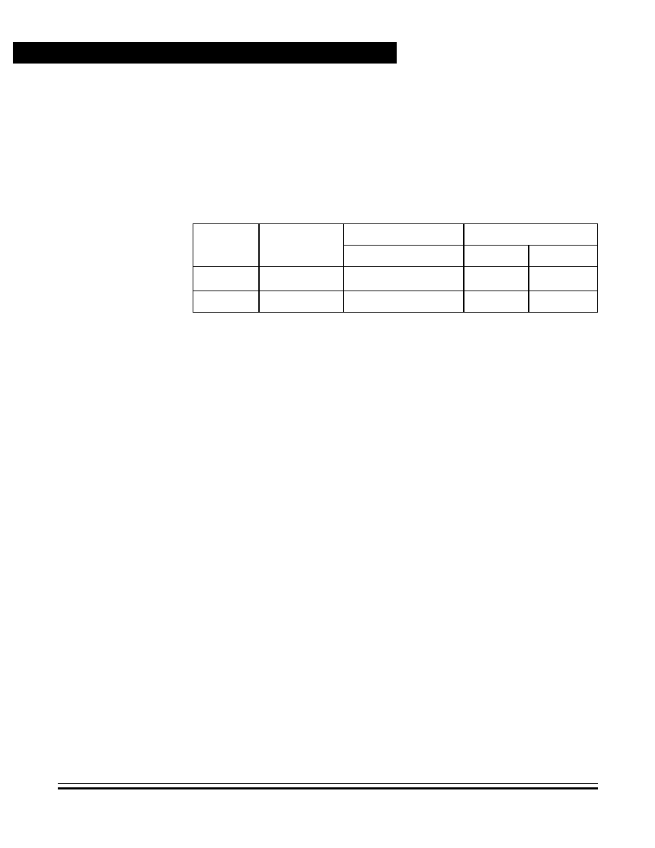
Technical Data
MC68HC705C8A -- Rev. 3
84
Parallel Input/Output (I/O)
MOTOROLA
Parallel Input/Output (I/O)
When a port B pin is programmed as an output, reading the port bit reads
the value of the data latch and not the voltage on the pin itself. When a
port B pin is programmed as an input, reading the port bit reads the
voltage level on the pin. The data latch can always be written, regardless
of the state of its DDRB bit.
NOTE:
To avoid excessive current draw, tie all unused input pins to V
DD
or V
SS
,
or for I/O pins change to outputs by writing to DDRB in user code as early
as possible.
Table 7-2. Port B Pin Functions
DDRB Bit
I/O Pin Mode
Accesses to DDRB
Accesses to PORTB
Read/Write
Read
Write
0
Input, Hi-Z
(1)
1. Hi-Z = high impedance
DDRB7≠DDRB0
Pin
PB7≠PB0
(2)
2. Writing affects data register but does not affect input.
1
Output
DDRB7≠DDRB0
PB7≠PB0
PB7≠PB0

Parallel Input/Output (I/O)
Port C
MC68HC705C8A -- Rev. 3
Technical Data
MOTOROLA
Parallel Input/Output (I/O)
85
7.5 Port C
Port C is an 8-bit, general-purpose, bidirectional I/O port. PC7 has a high
current sink and source capability.
7.5.1 Port C Data Register
The port C data register (PORTC) shown in
Figure 7-7
contains a data
latch for each of the eight port C pins. When a port C pin is programmed
to be an output, the state of its data register bit determines the state of
the output pin. When a port C pin is programmed to be an input, reading
the port C data register returns the logic state of the pin.
PC7≠PC0 -- Port C Data Bits
These read/write bits are software programmable. Data direction of
each bit is under the control of the corresponding bit in data direction
register C. PC7 has a high current sink and source capability. Reset
has no effect on port C data.
Address:
$0002
Bit 7
6
5
4
3
2
1
Bit 0
Read:
PC7
PC6
PC5
PC4
PC3
PC2
PC1
PC0
Write:
Reset:
Unaffected by reset
Figure 7-7. Port C Data Register (PORTC)

Technical Data
MC68HC705C8A -- Rev. 3
86
Parallel Input/Output (I/O)
MOTOROLA
Parallel Input/Output (I/O)
7.5.2 Data Direction Register C
The contents of data direction register C (DDRC) shown in
Figure 7-8
determine whether each port C pin is an input or an output. Writing a
logic 1 to a DDRC bit enables the output buffer for the associated port C
pin; a logic 0 disables the output buffer. A reset clears all DDRC bits,
configuring all port C pins as inputs.
DDRC7≠DDRC0 -- Port C Data Direction Bits
These read/write bits control port C data direction. Reset clears bits
DDRC7≠DDRC0.
1 = Corresponding port C pin configured as output
0 = Corresponding port C pin configured as input
NOTE:
Avoid glitches on port C pins by writing to the port C data register before
changing DDRC bits from logic 0 to logic 1.
Address:
$0006
Bit 7
6
5
4
3
2
1
Bit 0
Read:
DDRC7
DDRC6
DDRC5
DDRC4
DDRC3
DDRC2
DDRC1
DDRC0
Write:
Reset:
0
0
0
0
0
0
0
0
Figure 7-8. Data Direction Register C (DDRC)

Parallel Input/Output (I/O)
Port C
MC68HC705C8A -- Rev. 3
Technical Data
MOTOROLA
Parallel Input/Output (I/O)
87
7.5.3 Port C Logic
Figure 7-9
shows port C I/O logic.
Figure 7-9. Port C I/O Logic
When a port C pin is programmed as an output, reading the port bit reads
the value of the data latch and not the voltage on the pin. When a port C
pin is programmed as an input, reading the port bit reads the voltage
level on the pin. The data latch can always be written, regardless of the
state of its DDRC bit.
Table 7-3
summarizes the operation of the port C
pins.
NOTE:
To avoid excessive current draw, tie all unused input pins to V
DD
or V
SS
or change I/O pins to outputs by writing to DDRC in user code as early
as possible.
Table 7-3. Port C Pin Functions
DDRC Bit
I/O Pin Mode
Accesses to DDRC
Accesses to PORTC
Read/Write
Read
Write
0
Input, Hi-Z
(1)
1. Hi-Z = high impedance
DDRC7≠DDRC0
Pin
PC7≠PC0
(2)
2. Writing affects data register but does not affect input.
1
Output
DDRC7≠DDRC0
PC7≠PC0
PC7≠PC0
PCx
DATA DIRECTION
REGISTER C
BIT DDRCx
PORT C DATA
REGISTER
BIT PCx
READ $0006
WRITE $0002
READ $0002
RESET
I
N
T
E
R
N
AL
D
A
T
A
BU
S
WRITE $0006
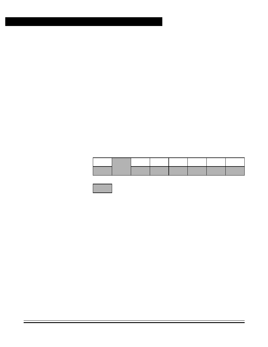
Technical Data
MC68HC705C8A -- Rev. 3
88
Parallel Input/Output (I/O)
MOTOROLA
Parallel Input/Output (I/O)
7.6 Port D
Port D is a 7-bit, special-purpose, input-only port that has no data
register. Reading address $0003 returns the logic states of the port D
pins.
Port D shares pins PD5≠PD2 with the serial peripheral interface module
(SPI). When the SPI is enabled, PD5≠PD2 read as logic 0s. When the
SPI is disabled, reading address $0003 returns the logic states of the
PD5≠PD2 pins.
Port D shares pins PD1 and PD0 with the SCI module. When the SCI is
enabled, PD1 and PD0 read as logic 0s. When the SCI is disabled,
reading address $0003 returns the logic states of the PD1 and PD0 pins.
Address:
$0003
Bit 7
6
5
4
3
2
1
Bit 0
Read:
PD7
SS
SCK
MOSI
MISO
TDO
RDI
Write:
Reset:
Unaffected by reset
= Unimplemented
Figure 7-10. Port D Fixed Input Register (PORTD)

MC68HC705C8A -- Rev. 3
Technical Data
MOTOROLA
Capture/Compare Timer
89
Technical Data -- MC68HC705C8A
Section 8. Capture/Compare Timer
8.1 Contents
8.2
Introduction . . . . . . . . . . . . . . . . . . . . . . . . . . . . . . . . . . . . . . . . 89
8.3
Timer Operation . . . . . . . . . . . . . . . . . . . . . . . . . . . . . . . . . . . . 89
8.3.1
Input Capture . . . . . . . . . . . . . . . . . . . . . . . . . . . . . . . . . . . . 92
8.3.2
Output Compare . . . . . . . . . . . . . . . . . . . . . . . . . . . . . . . . . .93
8.4
Timer I/O Registers. . . . . . . . . . . . . . . . . . . . . . . . . . . . . . . . . .94
8.4.1
Timer Control Register . . . . . . . . . . . . . . . . . . . . . . . . . . . . .94
8.4.2
Timer Status Register . . . . . . . . . . . . . . . . . . . . . . . . . . . . . 96
8.4.3
Timer Registers . . . . . . . . . . . . . . . . . . . . . . . . . . . . . . . . . . 97
8.4.4
Alternate Timer Registers. . . . . . . . . . . . . . . . . . . . . . . . . . . 98
8.4.5
Input Capture Registers . . . . . . . . . . . . . . . . . . . . . . . . . . 100
8.4.6
Output Compare Registers. . . . . . . . . . . . . . . . . . . . . . . . . 101
8.2 Introduction
This section describes the operation of the 16-bit capture/compare timer.
Figure 8-1
shows the structure of the timer module.
Figure 8-2
is a
summary of the timer input/output (I/O) registers.
8.3 Timer Operation
The core of the capture/compare timer is a 16-bit free-running counter.
The counter is the timing reference for the input capture and output
compare functions. The input capture and output compare functions can
latch the times at which external events occur, measure input
waveforms, and generate output waveforms and timing delays. Software
can read the value in the counter at any time without affecting the
counter sequence.

Technical Data
MC68HC705C8A -- Rev. 3
90
Capture/Compare Timer
MOTOROLA
Capture/Compare Timer
Figure 8-1. Timer Block Diagram
TCAP
EDGE
SELECT/
16-BIT COMPARATOR
OCRH ($0016)
OCRL ($0017)
16-BIT COUNTER
ATRH ($001A)
ATRL ($001B)
TCMP
DETECT
LOGIC
PIN
CONTROL
LOGIC
TRH ($0018)
TRL ($0019)
ICRH ($0014)
ICRL ($0015)
INTERNAL DATA BUS
TIMER CONTROL REGISTER
TIMER STATUS REGISTER
TIMER
INTERRUPT
REQUEST
INTERNAL CLOCK (XTAL
˜
2)
TO
F
OC
F
IC
F
$0013
$0012
ICI
E
OC
I
E
TO
I
E
IE
DG
OL
VL
OVE
R
F
L
OW
˜
4
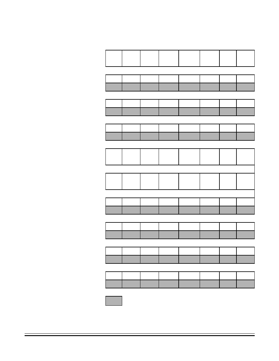
Capture/Compare Timer
Timer Operation
MC68HC705C8A -- Rev. 3
Technical Data
MOTOROLA
Capture/Compare Timer
91
Addr.
Register Name
Bit 7
6
5
4
3
2
1
Bit 0
$0012
Timer Control Register
(TCR)
See page 94.
Read:
ICIE
OCIE
TOIE
0
0
0
IEDG
OLVL
Write:
Reset:
0
0
0
0
0
0
U
0
$0013
Timer Status Register
(TSR)
See page 96.
Read:
ICF
OCF
TOF
0
0
0
0
0
Write:
Reset:
U
U
U
0
0
0
0
0
$0014
Input Capture Register
High (ICRH)
See page 100.
Read:
Bit 15
Bit 14
Bit 13
Bit 12
Bit 11
Bit 10
Bit 9
Bit 8
Write:
Reset:
Unaffected by reset
$0015
Input Capture Register
Low (ICRL)
See page 100.
Read:
Bit 7
Bit 6
Bit 5
Bit 4
Bit 3
Bit 2
Bit 1
Bit 0
Write:
Reset:
Unaffected by reset
$0016
Output Compare Register
High (OCRH)
See page 101.
Read:
Bit 15
Bit 14
Bit 13
Bit 12
Bit 11
Bit 10
Bit 9
Bit 8
Write:
Reset:
Unaffected by reset
$0017
Output Compare Register
Low (OCRL)
See page 101.
Read:
Bit 7
Bit 6
Bit 5
Bit 4
Bit 3
Bit 2
Bit 1
Bit 0
Write:
Reset:
Unaffected by reset
$0018
Timer Register High
(TRH)
See page 97.
Read:
Bit 15
Bit 14
Bit 13
Bit 12
Bit 11
Bit 10
Bit 9
Bit 8
Write:
Reset:
Reset initializes TRH to $FF
$0019
Timer Register Low
(TRL)
See page 97.
Read:
Bit 7
Bit 6
Bit 5
Bit 4
Bit 3
Bit 2
Bit 1
Bit 0
Write:
Reset:
Reset initializes TRL to $FC
$001A
Alternate Timer Register
High (ATRH)
See page 99.
Read:
Bit 15
Bit 14
Bit 13
Bit 12
Bit 11
Bit 10
Bit 9
Bit 8
Write:
Reset:
Reset initializes ATRH to $FF
$001B
Alternate Timer Register
Low (ATRL)
See page 99.
Read:
Bit 7
Bit 6
Bit 5
Bit 4
Bit 3
Bit 2
Bit 1
Bit 0
Write:
Reset:
Reset initializes ATRL to $FC
= Unimplemented
U = Unaffected
Figure 8-2. Timer I/O Register Summary
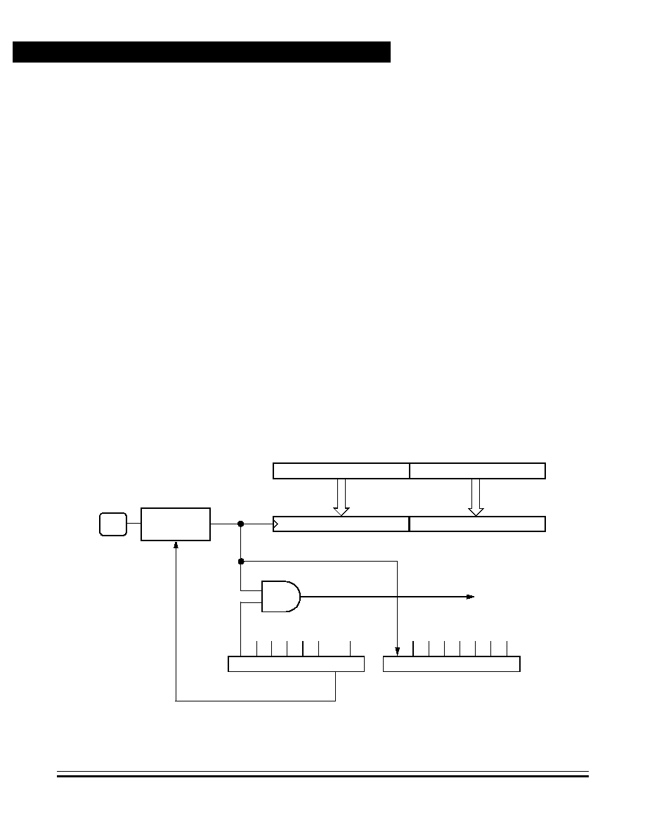
Technical Data
MC68HC705C8A -- Rev. 3
92
Capture/Compare Timer
MOTOROLA
Capture/Compare Timer
Because of the 16-bit timer architecture, the I/O registers for the input
capture and output compare functions are pairs of 8-bit registers.
Because the counter is 16 bits long and preceded by a fixed
divide-by-four prescaler, the counter rolls over every 262,144 internal
clock cycles. Timer resolution with a 4-MHz crystal is 2
µ
s.
8.3.1 Input Capture
The input capture function can record the time at which an external event
occurs. When the input capture circuitry detects an active edge on the
input capture pin (TCAP), it latches the contents of the timer registers
into the input capture registers. The polarity of the active edge is
programmable.
Latching values into the input capture registers at successive edges of
the same polarity measures the period of the input signal on the TCAP
pin. Latching the counter values at successive edges of opposite polarity
measures the pulse width of the signal.
Figure 8-3
shows the logic of the
input capture function.
Figure 8-3. Input Capture Operation
TCAP
EDGE
SELECT/DETECT
INPUT CAPTURE REGISTER HIGH
INPUT CAPTURE REGISTER LOW
TIMER REGISTER HIGH
TIMER REGISTER LOW
TIMER
INTERRUPT
REQUEST
LOGIC
15
$0018
8
7
$0019
0
15
8
7
0
$0014
$0015
TIMER STATUS REGISTER
TIMER CONTROL REGISTER
LATCH
IE
DG
$0012
$0013
IC
F
OC
F
TO
F
IC
IE
OC
I
E
TO
I
E
OL
V
L
Capture/Compare Timer
Timer Operation
MC68HC705C8A -- Rev. 3
Technical Data
MOTOROLA
Capture/Compare Timer
93
8.3.2 Output Compare
The output compare function can generate an output signal when the
16-bit counter reaches a selected value. Software writes the selected
value into the output compare registers. On every fourth internal clock
cycle the output compare circuitry compares the value of the counter to
the value written in the output compare registers. When a match occurs,
the timer transfers the programmable output level bit (OLVL) from the
timer control register to the output compare pin (TCMP).
Software can use the output compare register to measure time periods,
to generate timing delays, or to generate a pulse of specific duration or
a pulse train of specific frequency and duty cycle on the TCMP pin.
Figure 8-4
shows the logic of the output compare function.
Figure 8-4. Output Compare Operation
16-BIT COMPARATOR
OUTPUT COMPARE REGISTER HIGH
OUTPUT COMPARE REGISTER LOW
COUNTER HIGH BYTE
COUNTER LOW BYTE
PIN
CONTROL
LOGIC
TCMP
TIMER STATUS REGISTER
TIMER STATUS REGISTER
15
0
15
8
7
0
TIMER
INTERRUPT
REQUEST
IC
IE
OC
I
E
TO
I
E
IC
F
OC
F
TO
F
$0012
$0013
$0016
$0017

Technical Data
MC68HC705C8A -- Rev. 3
94
Capture/Compare Timer
MOTOROLA
Capture/Compare Timer
8.4 Timer I/O Registers
These registers control and monitor the timer operation:
∑
Timer control register (TCR)
∑
Timer status register (TSR)
∑
Timer registers (TRH and TRL)
∑
Alternate timer registers (ATRH and ATRL)
∑
Input capture registers (ICRH and ICRL)
∑
Output compare registers (OCRH and OCRL)
8.4.1 Timer Control Register
The timer control register (TCR) as shown in
Figure 8-5
performs these
functions:
∑
Enables input capture interrupts
∑
Enables output compare interrupts
∑
Enables timer overflow interrupts
∑
Controls the active edge polarity of the TCAP signal
∑
Controls the active level of the TCMP output
Address:
$0012
Bit 7
6
5
4
3
2
1
Bit 0
Read:
ICIE
OCIE
TOIE
0
0
0
IEDG
OLVL
Write:
Reset:
0
0
0
0
0
0
U
0
U = Unaffected
Figure 8-5. Timer Control Register (TCR)

Capture/Compare Timer
Timer I/O Registers
MC68HC705C8A -- Rev. 3
Technical Data
MOTOROLA
Capture/Compare Timer
95
ICIE -- Input Capture Interrupt Enable Bit
This read/write bit enables interrupts caused by an active signal on
the TCAP pin. Reset clears the ICIE bit.
1 = Input capture interrupts enabled
0 = Input capture interrupts disabled
OCIE -- Output Compare Interrupt Enable Bit
This read/write bit enables interrupts caused by an active signal on
the TCMP pin. Reset clears the OCIE bit.
1 = Output compare interrupts enabled
0 = Output compare interrupts disabled
TOIE -- Timer Overflow Interrupt Enable Bit
This read/write bit enables interrupts caused by a timer overflow.
Reset clears the TOIE bit.
1 = Timer overflow interrupts enabled
0 = Timer overflow interrupts disabled
IEDG -- Input Edge Bit
The state of this read/write bit determines whether a positive or
negative transition on the TCAP pin triggers a transfer of the contents
of the timer register to the input capture registers. Reset has no effect
on the IEDG bit.
1 = Positive edge (low-to-high transition) triggers input capture
0 = Negative edge (high-to-low transition) triggers input capture
OLVL -- Output Level Bit
The state of this read/write bit determines whether a logic 1 or a
logic 0 appears on the TCMP pin when a successful output compare
occurs. Reset clears the OLVL bit.
1 = TCMP goes high on output compare
0 = TCMP goes low on output compare
Bits 4≠2 -- Not used; these bits always read 0
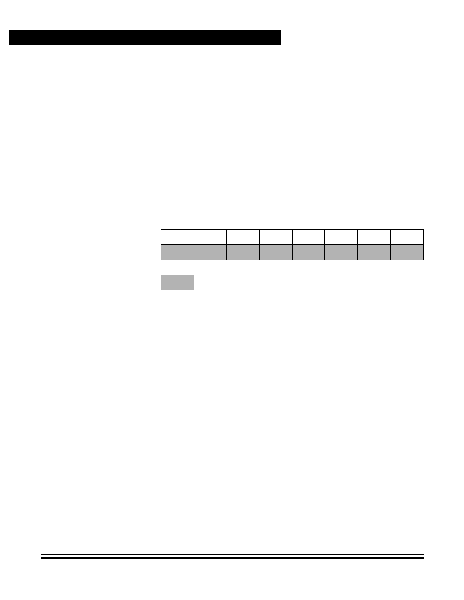
Technical Data
MC68HC705C8A -- Rev. 3
96
Capture/Compare Timer
MOTOROLA
Capture/Compare Timer
8.4.2 Timer Status Register
The timer status register (TSR) is a read-only register shown in
Figure 8-6
contains flags for these events:
∑
An active signal on the TCAP pin, transferring the contents of the
timer registers to the input capture registers
∑
A match between the 16-bit counter and the output compare
registers, transferring the OLVL bit to the TCMP pin
∑
A timer rollover from $FFFF to $0000
ICF -- Input Capture Flag
The ICF bit is set automatically when an edge of the selected polarity
occurs on the TCAP pin. Clear the ICF bit by reading the timer status
register with ICF set and then reading the low byte ($0015) of the
input capture registers. Reset has no effect on ICF.
1 = Input capture
0 = No input capture
OCF -- Output Compare Flag
The OCF bit is set automatically when the value of the timer registers
matches the contents of the output compare registers. Clear the OCF
bit by reading the timer status register with OCF set and then reading
the low byte ($0017) of the output compare registers. Reset has no
effect on OCF.
1 = Output compare
0 = No output compare
Address:
$0013
Bit 7
6
5
4
3
2
1
Bit 0
Read:
ICF
OCF
TOF
0
0
0
0
0
Write:
Reset:
U
U
U
0
0
0
0
0
= Unimplemented
U = Unaffected
Figure 8-6. Timer Status Register (TSR)
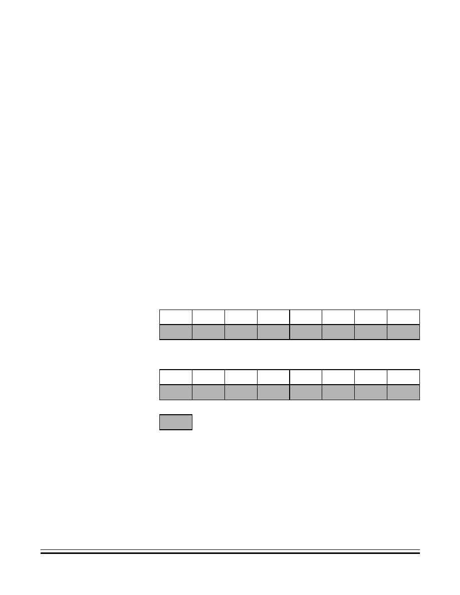
Capture/Compare Timer
Timer I/O Registers
MC68HC705C8A -- Rev. 3
Technical Data
MOTOROLA
Capture/Compare Timer
97
TOF -- Timer Overflow Flag
The TOF bit is automatically set when the 16-bit counter rolls over
from $FFFF to $0000. Clear the TOF bit by reading the timer status
register with TOF set and then reading the low byte ($0019) of the
timer registers. Reset has no effect on TOF.
1 = Timer overflow
0 = No timer overflow
Bits 4≠0 -- Not used; these bits always read 0
8.4.3 Timer Registers
The read-only timer registers (TRH and TRL) shown in
Figure 8-7
contain the current high and low bytes of the 16-bit counter. Reading
TRH before reading TRL causes TRL to be latched until TRL is read.
Reading TRL after reading the timer status register clears the timer
overflow flag bit (TOF). Writing to the timer registers has no effect.
Bit 7
6
5
4
3
2
1
Bit 0
Register Name and Address: Timer Register High -- $0018
Read:
Bit 15
Bit 14
Bit 13
Bit 12
Bit 11
Bit 10
Bit 9
Bit 8
Write:
Reset:
Reset initializes TRH to $FF
Register Name and Address: Timer Register Low -- $0019
Read:
Bit 7
Bit 6
Bit 5
Bit 4
Bit 3
Bit 2
Bit 1
Bit 0
Write:
Reset:
Reset initializes TRL to $FC
= Unimplemented
Figure 8-7. Timer Registers (TRH and TRL)
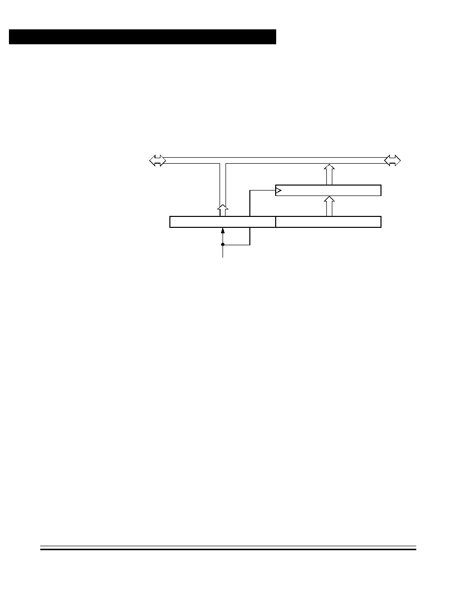
Technical Data
MC68HC705C8A -- Rev. 3
98
Capture/Compare Timer
MOTOROLA
Capture/Compare Timer
Reading TRH returns the current value of the high byte of the counter
and causes the low byte to be latched into a buffer, as shown in
Figure 8-8
. The buffer value remains fixed even if the high byte is read
more than once. Reading TRL reads the transparent low byte buffer and
completes the read sequence of the timer registers.
Figure 8-8. Timer Register Reads
NOTE:
To prevent interrupts from occurring between readings of TRH and TRL,
set the interrupt mask (I bit) in the condition code register before reading
TRH, and clear the mask after reading TRL.
8.4.4 Alternate Timer Registers
The alternate timer registers (ATRH and ATRL) shown in
Figure 8-9
contain the current high and low bytes of the 16-bit counter. Reading
ATRH before reading ATRL causes ATRL to be latched until ATRL is
read. Reading does not affect the timer overflow flag (TOF). Writing to
the alternate timer registers has no effect.
LOW BYTE BUFFER
$0018
$0019
TIMER REGISTER HIGH
TIMER REGISTER LOW
READ TRH
LATCH
INTERNAL DATA BUS
15
7
0
0
7
8
Capture/Compare Timer
Timer I/O Registers
MC68HC705C8A -- Rev. 3
Technical Data
MOTOROLA
Capture/Compare Timer
99
Reading ATRH returns the current value of the high byte of the counter
and causes the low byte to be latched into a buffer, as shown in
Figure 8-10
.
Figure 8-10. Alternate Timer Register Reads
NOTE:
To prevent interrupts from occurring between readings of ATRH and
ATRL, set the interrupt mask (I bit) in the condition code register before
reading ATRH, and clear the mask after reading ATRL.
Bit 7
6
5
4
3
2
1
Bit 0
Register Name and Address: Alternate Timer Register High -- $001A
Read:
Bit 15
Bit 14
Bit 13
Bit 12
Bit 11
Bit 10
Bit 9
Bit 8
Write:
Reset:
Reset initializes ATRH to $FF
Register Name and Address: Alternate Timer Register Low -- $001B
Read:
Bit 7
Bit 6
Bit 5
Bit 4
Bit 3
Bit 2
Bit 1
Bit 0
Write:
Reset:
Reset initializes ATRL to $FC
= Unimplemented
Figure 8-9. Alternate Timer Registers (ATRH and ATRL)
LOW BYTE BUFFER
$001A
$001B
READ ATRH
LATCH
INTERNAL DATA BUS
15
7
0
0
7
8
ALTERNATE TIMER REGISTER HIGH
ALTERNATE TIMER REGISTER LOW

Technical Data
MC68HC705C8A -- Rev. 3
100
Capture/Compare Timer
MOTOROLA
Capture/Compare Timer
8.4.5 Input Capture Registers
When a selected edge occurs on the TCAP pin, the current high and low
bytes of the 16-bit counter are latched into the read-only input capture
registers (ICRH and ICRL) shown in
Figure 8-11
. Reading ICRH before
reading ICRL inhibits further captures until ICRL is read. Reading ICRL
after reading the timer status register clears the input capture flag (ICF).
Writing to the input capture registers has no effect.
NOTE:
To prevent interrupts from occurring between readings of ICRH and
ICRL, set the interrupt mask (I bit) in the condition code register before
reading ICRH and clear the mask after reading ICRL.
Bit 7
6
5
4
3
2
1
Bit 0
Register Name and Address: Input Capture Register High -- $0014
Read:
Bit 15
Bit 14
Bit 13
Bit 12
Bit 11
Bit 10
Bit 9
Bit 8
Write:
Reset:
Unaffected by reset
Register Name and Address: Input Capture Register Low -- $0015
Read:
Bit 7
Bit 6
Bit 5
Bit 4
Bit 3
Bit 2
Bit 1
Bit 0
Write:
Reset:
Unaffected by reset
= Unimplemented
Figure 8-11. Input Capture Registers (ICRH and ICRL)
Capture/Compare Timer
Timer I/O Registers
MC68HC705C8A -- Rev. 3
Technical Data
MOTOROLA
Capture/Compare Timer
101
8.4.6 Output Compare Registers
When the value of the 16-bit counter matches the value in the read/write
output compare registers (OCRH and OCRL) shown in
Figure 8-12
, the
planned TCMP pin action takes place. Writing to OCRH before writing to
OCRL inhibits timer compares until OCRL is written. Reading or writing
to OCRL after reading the timer status register clears the output
compare flag (OCF).
To prevent OCF from being set between the time it is read and the time
the output compare registers are updated, use this procedure:
1. Disable interrupts by setting the I bit in the condition code register.
2. Write to OCRH. Compares are now inhibited until OCRL is written.
3. Clear bit OCF by reading the timer status register (TSR).
4. Enable the output compare function by writing to OCRL.
5. Enable interrupts by clearing the I bit in the condition code register.
Bit 7
6
5
4
3
2
1
Bit 0
Register Name and Address: Output Compare Register High -- $0016
Read:
Bit 15
Bit 14
Bit 13
Bit 12
Bit 11
Bit 10
Bit 9
Bit 8
Write:
Reset:
Unaffected by reset
Register Name and Address: Output Compare Register Low -- $0017
Read:
Bit 7
Bit 6
Bit 5
Bit 4
Bit 3
Bit 2
Bit 1
Bit 0
Write:
Reset:
Unaffected by reset
Figure 8-12. Output Compare Registers (OCRH and OCRL)

Technical Data
MC68HC705C8A -- Rev. 3
102
Capture/Compare Timer
MOTOROLA
Capture/Compare Timer

MC68HC705C8A -- Rev. 3
Technical Data
MOTOROLA
EPROM/OTPROM (PROM)
103
Technical Data -- MC68HC705C8A
Section 9. EPROM/OTPROM (PROM)
9.1 Contents
9.2
Introduction . . . . . . . . . . . . . . . . . . . . . . . . . . . . . . . . . . . . . . . 103
9.3
EPROM/OTPROM (PROM) Programming . . . . . . . . . . . . . . . 104
9.3.1
Program Register . . . . . . . . . . . . . . . . . . . . . . . . . . . . . . . . 109
9.3.2
Preprogramming Steps . . . . . . . . . . . . . . . . . . . . . . . . . . . 110
9.4
PROM Programming Routines . . . . . . . . . . . . . . . . . . . . . . . . 111
9.4.1
Program and Verify PROM. . . . . . . . . . . . . . . . . . . . . . . . . 111
9.4.2
Verify PROM Contents . . . . . . . . . . . . . . . . . . . . . . . . . . . .112
9.4.3
Secure PROM . . . . . . . . . . . . . . . . . . . . . . . . . . . . . . . . . . 112
9.4.4
Secure PROM and Verify . . . . . . . . . . . . . . . . . . . . . . . . . . 113
9.4.5
Secure PROM and Dump. . . . . . . . . . . . . . . . . . . . . . . . . . 113
9.4.6
Load Program into RAM and Execute . . . . . . . . . . . . . . . . 114
9.4.7
Execute Program in RAM. . . . . . . . . . . . . . . . . . . . . . . . . . 115
9.4.8
Dump PROM Contents. . . . . . . . . . . . . . . . . . . . . . . . . . . .115
9.5
Control Registers . . . . . . . . . . . . . . . . . . . . . . . . . . . . . . . . . . 116
9.5.1
Option Register . . . . . . . . . . . . . . . . . . . . . . . . . . . . . . . . . 116
9.5.2
Mask Option Register 1 . . . . . . . . . . . . . . . . . . . . . . . . . . . 117
9.5.3
Mask Option Register 2 . . . . . . . . . . . . . . . . . . . . . . . . . . . 118
9.6
EPROM Erasing . . . . . . . . . . . . . . . . . . . . . . . . . . . . . . . . . . . 119
9.2 Introduction
This section describes erasable, programmable read-only
memory/one-time programmable read-only memory (EPROM/OTPROM
(PROM)) programming.

Technical Data
MC68HC705C8A -- Rev. 3
104
EPROM/OTPROM (PROM)
MOTOROLA
EPROM/OTPROM (PROM)
9.3 EPROM/OTPROM (PROM) Programming
The internal PROM can be programmed efficiently using the Motorola
MC68HC05PGMR-2 programmer board, which can be purchased from
a Motorola-authorized distributor. The user can program the
microcontroller unit (MCU) using this printed circuit board (PCB) in
conjunction with an EPROM device already programmed with user code.
Only standalone programming is discussed in this section. For more
information concerning the MC68HC05PGMR and its usages, contact a
local Motorola representative for a copy of the MC68HC05PGMR
Programmer Board User's Manual #2, Motorola document number
MC68HC05PGMR2/D1.
Refer to
Figure 9-1
for an EPROM programming flowchart.
Figure 9-2
provides a schematic of the MC68HC05PGMR PCB with the reference
designators defined in
Table 9-1
.
Table 9-1. MC68HC05PGMR PCB Reference Designators
Reference
Designators
Device
Type
Ground
+5 V
+12 V
≠12 V
V
PP
Notes
U1
2764
14, 20
1, 26, 27, 28
--
--
--
8 K x 8-bit EPROM
U2
MCU
20
40
--
--
3
40-pin DIP socket
U3
MCU
22
44
--
--
4 44-lead
PLCC
socket
U4
MC145406
9
16
1
8
-- Driver/receiver
VR1
NMA0512S
2.5
1
6
4
-- DC-DC
converter

EPROM/OTPROM (PROM)
EPROM/OTPROM (PROM) Programming
MC68HC705C8A -- Rev. 3
Technical Data
MOTOROLA
EPROM/OTPROM (PROM)
105
Figure 9-1. EPROM/OTPROM Programming Flowchart
YES
NO
START
APPLY V
PP
NTRYS = 0
START AT BEGINNING
OF MEMORY
LAT = 1
WRITE PROM DATA
PGM = 1
WAIT 1 ms
PGM = 0
LAT = 0
WRITE
ADDITIONAL
BYTE
NTRYS = NTRYS + 1
NTRYS = 2
V
PP
OFF
END
YES
NO

Technical Data
MC68HC705C8A -- Rev. 3
106
EPROM/OTPROM (PROM)
MOTOROLA
EPROM/OTPROM (PROM)
Figure 9-2. PROM Programming Circuit
1. The asterisk (*) denotes option T
4
2
3
5
1
1
5
6
4
2
+
3
30
3
3
P3
1
8
29
2
2
16
9
14
15
5
6
8
20
1
7
1
26
28
20
25
22
24
21
23
2
+12 V
OFF
ON
S1
P1
+5 V
+12 V
≠12 V
V
PP
GND
RXD
TXD
CTS
DSR
DCD
DTR
GND
GND
U4
MC145406
+12 V
≠12 V
+5 V
ON
OFF
VR1 NMA0512S
DC-DC CONVERTER
(OPTIONAL)
V
CC
0 V
+V
≠V
GND
≠12 V
D1
1N4001
PD1
PD0
U1
2764
V
PP
+5 V
NC
V
CC
C5
0.1
µ
F
PGM
CE
(A10)
(A11)
(A12)
A8
A9
A10
A11
OE
GND
14
D0
10
9
8
7
6
5
4
3
(A0)
(A1)
(A2)
(A3)
(A4)
(A5)
(A6)
(A7)
11
12
13
15
16
17
18
19
R15
10 K
PA0
PA1
PA2
PA3
PA4
PA5
PA6
PA7
PB0
PB1
PB2
PB3
PB4
PB5
PB6
PB7
40
V
DD
V
PP
PD1
PD0
PA0
11
10
9
8
7
6
5
4
12
13
14
15
16
17
18
19
20
V
SS
PB1
PB0
PA7
PA6
PA5
PA4
PA3
PA2
U2
40-PIN DIP
SOCKET
PA1
+5 V
C1
100
µ
F
OSC1
39
OSC2
38
RESET
1
IRQ
2
TCAP
37
PD7
36
TCMP
35
PD5
34
PD4
33
PD2
32
31
PC5
PC6
PC0
PC1
PC2
PC3
PC4
23
22
28
27
26
25
24
(A8)
(A9)
(A10)
(A11)
(A12)
PC7
21
M
N
L
K
J
I
H
G
F
E
D
C
B
A
(ENABLE)
(A8)
(A9)
(D3)
(D2)
(D1)
(D0)
(D4)
(D5)
(D6)
(D7)
O
P
Q
R
S
PD3
PB2
PB3
PB4
PB5
PB6
PB7
A0
A1
A2
A3
A4
A5
A6
A7
27
D1
D2
D3
D4
D5
D6
D7
V
PP
A12
Notes:
2. Unless otherwise specified, resistors are in ohms,
3. Device type numbers shown in circuit are for
command only.
±
5% 1/4 W; capacitors are in
µ
F; voltages are dc.
reference only. Device type number varies
with manufacturer.
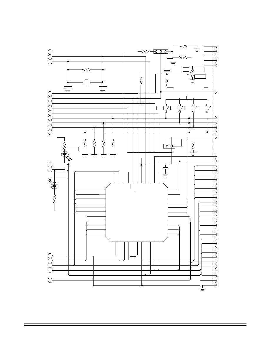
EPROM/OTPROM (PROM)
EPROM/OTPROM (PROM) Programming
MC68HC705C8A -- Rev. 3
Technical Data
MOTOROLA
EPROM/OTPROM (PROM)
107
Figure 9-2. PROM Programming Circuit (Continued)
1
2
3
1 2
A
B
C
D
E
F
G
H
I
J
K
L
+5 V
R10*
470
DS2*
M
N
VERF
(VERF)
(PROG)
PROG
DS1*
R11*
470
+5 V
O
P
Q
R
S
(D4)
(D3)
(D2)
(D1)
(D0)
(A0)
(A1)
(A2)
(A3)
(A4)
(A5)
17
15
16
14
13
12
11
10
9
8
7
PB4
PB3
PB2
PB1
PB0
PA0
PA1
PA2
PA3
PA4
PA5
C4
22 pF
R5
10 M
C3
22
pF
2.0 MHz
Y1
R13
10 K
+5 V
+5 V
R3 10 K
R9
10 K
R8
10 K
R7
10 K
R6
10 K
PA6
PA7
V
PP
NC
IR
Q
R
ESET
V
DD
OS
C
1
OS
C
2
TC
A
P
NC
PD7
TCMP
PD5
PD4
PD3
PD2
PD1
PD0
PC0
PC1
PC2
U3
44-LEAD PLCC
SOCKET
C6
0.1
µ
F
NC
PB5
PB6
PB7
V
SS
NC
PC
7
PC
6
PC
5
PC
4
PC
3
39
38
37
36
35
34
33
32
31
30
29
18
NC
19
20
21
22
23
24
25
(PR
O
G
)
26
27
28
(VER
F
)
(D
5
)
(D
6
)
(D
7
)
NC
(A1
2
)
(
A
11)
(A10)
(A9)
(A8)
PD0
PD1
PD2
PD3
PD4
PD5
(A6
)
6
(A7
)
5
4
3
NC
2
1
44
43
42
41
40
NC
+5 V
PC7
PC6
PC5
PD0
PD1
PC4
PC3
PC2
PC1
PC0
PA7
PA6
PA5
PA4
PA3
PA2
PA1
PA0
PB7
PB6
PB5
PB4
PB3
PB2
PB1
PB0
TCMP
TCAP
37
35
12
13
14
15
16
17
18
19
11
10
9
8
7
6
5
4
28
27
26
25
24
30
29
23
22
21
R12
10 K
PD7
PD2
PD3
PD4
PD5
34
33
32
31
36
S6
S5
S4
S3
+5 V
J2
+5 V
IRQ
RESET
2
+5 V
R4
10 K
40
39
38
3
1
P2
NC
NC
NC
NC
NC
+12 V
R2
10 K
2.7 K
R1
NC
OUT
1.0
µ
F
C2
S2
J1
20
V
SS

Technical Data
MC68HC705C8A -- Rev. 3
108
EPROM/OTPROM (PROM)
MOTOROLA
EPROM/OTPROM (PROM)
To program the PROM MCU, the MCU is installed in the PCB, along with
an EPROM device programmed with user code; the MCU is then
subjected to a series of routines. The routines necessary to program,
verify, and secure the PROM MCU are:
∑
Program and verify PROM
∑
Verify PROM contents only
∑
Secure PROM and verify
∑
Secure PROM and dump through the serial communications
interface (SCI)
Other board routines available to the user are:
∑
Load program into random-access memory (RAM) and execute
∑
Execute program in RAM
∑
Dump PROM contents (binary upload)
The user first configures the MCU for the bootstrap mode of operations
by installing a fabricated jumper across pins 1 and 2 of the board's mode
select header, J1. Next, the board's mode switches (S3, S4, S5, and S6)
are set to determine the routine to be executed after the next reset, as
shown in
Table 9-2
.
Table 9-2. PROM Programming Routines
Routine
S3
S4
S5
S6
Program and verify PROM
Off
Off
Off
Off
Verify PROM contents only
Off
Off
On
Off
Secure PROM contents and verify
On
Off
On
Off
Secure PROM contents and dump
On
On
On
Off
Load program into RAM and execute
Off
On
Off
Off
Execute program in RAM
Off
Off
Off
On
Dump PROM contents
Off
On
On
Off

EPROM/OTPROM (PROM)
EPROM/OTPROM (PROM) Programming
MC68HC705C8A -- Rev. 3
Technical Data
MOTOROLA
EPROM/OTPROM (PROM)
109
9.3.1 Program Register
The program register (PROG) shown in
Figure 9-3
is used for PROM
programming.
LAT -- Latch Enable Bit
This bit is both readable and writable.
1 = Enables PROM data and address bus latches for programming
on the next byte write cycle
0 = Latch disabled. PROM data and address buses are unlatched
for normal CPU operations.
PGM -- Program Bit
If LAT is cleared, PGM cannot be set.
1 = Enables V
PP
power to the PROM for programming
0 = V
PP
is disabled.
Bits 1 and 3
-
7 -- Not used; always read 0
Address:
$001C
Bit 7
6
5
4
3
2
1
Bit 0
Read:
0
0
0
0
0
LAT
0
PGM
Write:
Reset:
0
0
0
0
0
0
0
0
Figure 9-3. Program Register (PROG)

Technical Data
MC68HC705C8A -- Rev. 3
110
EPROM/OTPROM (PROM)
MOTOROLA
EPROM/OTPROM (PROM)
9.3.2 Preprogramming Steps
Before programming the PROM using an MC68HC05PGMR PCB in
standalone mode, the user should ensure that:
∑
A jumper is installed on pins 1 and 2 of mode select header J1.
∑
An EPROM is programmed with the necessary user code.
∑
The erasure window (if any) of the device to be programmed is
covered.
∑
V
DD
of +5 Vdc is available on the board.
∑
V
PP
is available on the board.
NOTE:
If the V
PP
level at the MCU exceeds +16 Vdc, then the MC68HC705C8A
MCU device will suffer permanent damage.
Once those conditions are met, the user should take these steps before
beginning programming:
1. Remove the V
PP
power source.
2. Set switch 1 in the OFF position (removes V
DD
).
3. Place the programmed EPROM in socket U1.
4. Insert the erased PROM MCU device to be programmed in the
proper socket:
≠
MC68HC705C8S or MC68HC705C8P in socket U2 (40-pin
dual in-line package (DIP)) or
≠
MC68HC705C8FN in socket U3 (44-pin plastic leaded chip
carrier (PLCC)) with the device notch at the upper right corner
of the socket.
5. Set switch S2 in the RESET position.
NOTE:
No PROM MCU should be inserted in or removed from its board socket
(U2 or U3) while V
PP
(P1, slot 5) or V
DD
(switch 1) is active on the board.

EPROM/OTPROM (PROM)
PROM Programming Routines
MC68HC705C8A -- Rev. 3
Technical Data
MOTOROLA
EPROM/OTPROM (PROM)
111
9.4 PROM Programming Routines
This subsection describes the routines necessary to program, verify, and
secure the PROM device, and other routines available to the user.
9.4.1 Program and Verify PROM
The program and verify PROM routine copies the contents of the
external EPROM into the MCU PROM with direct correspondence
between the addresses. Memory addresses in the MCU that are not
implemented in PROM are skipped. Unprogrammed addresses in the
EPROM being copied should contain $00 bytes to speed up the
programming process.
To run the program and verify the PROM routine on the PROM MCU,
take these steps:
1. Set switch 1 in the ON position (restores V
DD
).
2. Restore the V
PP
power source.
3. Set switches S3, S4, S5, and S6 in the OFF position (selects
proper routine).
4. Set switch 2 in the OUT position (routine is activated).
The red light-emitting diode (LED) is illuminated, showing that the
programming part of the routine is running. The LED goes out
when programming is finished. The verification part of the routine
now begins. When the green LED is illuminated, verification is
successfully completed and the routine is finished.
5. Set switch 2 in the RESET position.
At this point, if no other MCU is to be programmed or secured, remove
V
PP
power from the board. If another routine is to be performed on the
MCU being programmed, the user can then set switches S3, S4, S5, and
S6 to the positions necessary to select the next routine, and begin the
routine by setting switch 2 to the OUT position. If no other routine is to
be performed, remove V
DD
from the board and remove the MCU from
the programming socket.

Technical Data
MC68HC705C8A -- Rev. 3
112
EPROM/OTPROM (PROM)
MOTOROLA
EPROM/OTPROM (PROM)
9.4.2 Verify PROM Contents
The verify PROM contents routine is normally run automatically after the
PROM is programmed. Direct entry to this routine causes the PROM
contents of the MCU to be compared to the contents of the external
memory locations of the EPROM at the same addresses.
To invoke the verify PROM contents routine of the MCU, take these
steps:
1. Set switch 1 in the ON position (restores V
DD
).
2. Connect V
PP
to V
DD
.
3. Set switches S3, S4, and S6 in the OFF position.
4. Set S5 in the ON position.
5. Set switch 2 in the OUT position (routine is activated).
The red LED is not illuminated during this routine, since no
programming takes place. If verification fails, the routine halts with
the failing address in the external memory bus. When the green
LED is illuminated, verification is completed successfully and the
routine is finished.
6. Set switch 2 in the RESET position.
At this point, if another routine is to be performed on the MCU being
programmed, the user can set switches S3, S4, S5, and S6 to the
positions necessary to select the next routine and move switch S2 to the
OUT position to start the routine. If no other routine is to be performed,
remove V
DD
from the board and remove the MCU from the programming
socket.
9.4.3 Secure PROM
The secure PROM routines are used after the PROM is successfully
programmed and verified. Only the SEC bit of the option register
($1FDF) is programmed, but V
PP
is necessary. Once this bit is
programmed, PROM is secure and can be neither verified nor dumped.

EPROM/OTPROM (PROM)
PROM Programming Routines
MC68HC705C8A -- Rev. 3
Technical Data
MOTOROLA
EPROM/OTPROM (PROM)
113
9.4.4 Secure PROM and Verify
This routine is used after the PROM is programmed successfully to
verify the contents of the MCU PROM against the contents of the
EPROM and then to secure the PROM. To accomplish this routine, take
these steps:
1. Set switch 1 in the ON position (restores V
DD
).
2. Restore V
PP
power to the programming board.
3. Set switches S4 and S6 in the OFF position.
4. Set switches S3 and S5 in the ON position.
5. Set switch 2 in the OUT position (routine is activated).
Execution time for this routine is about one second.
6. Set switch 2 in the RESET position when the routine is completed.
No LED is illuminated during this routine. Further, the end of the routine
does not mean that the SEC bit was verified. To ensure that security is
properly enabled, attempt to perform another verify routine. If the green
LED does not light, the PROM has been secured properly.
9.4.5 Secure PROM and Dump
This routine is used after the PROM is successfully programmed to
dump the contents of the MCU PROM through the SCI (binary upload)
and then to secure the PROM. To accomplish this routine, take these
steps:
1. Set switch 1 in the ON position (restores V
DD
).
2. Restore V
PP
power to the programming board.
3. Set switch S6 in the OFF position.
4. Set switches S3, S4, and S5 in the ON position.
5. Set switch 2 in the OUT position (routine is activated).
Execution time for this routine is about one second.
6. Set switch 2 in the RESET position when the routine is completed.

Technical Data
MC68HC705C8A -- Rev. 3
114
EPROM/OTPROM (PROM)
MOTOROLA
EPROM/OTPROM (PROM)
No LED is illuminated during this routine. Further, the end of the routine
does not mean that the SEC bit was verified. To ensure that security is
properly enabled, attempt to perform another verify routine. If the green
LED does not light, the PROM has been secured properly.
9.4.6 Load Program into RAM and Execute
In the load program in RAM and execute routine, user programs are
loaded via the SCI port and then executed. Data is loaded sequentially
starting at address $0050. After the last byte is loaded, control is
transferred to the RAM program starting at $0051. The first byte loaded
is the count of the total number of bytes in the program plus the count
byte. The program starts at location $0051 in RAM. During initialization,
the SCI is configured for eight data bits and one stop bit. The baud rate
is 4800 with a 2-MHz crystal or 9600 with a 4-MHz crystal.
To load a program into RAM and execute it, take these steps:
1. Set switch 1 in the ON position (restores V
DD
).
2. Connect V
PP
to V
DD
.
3. Set switches S3, S5, and S6 in the OFF position.
4. Set switch S4 in the ON position.
5. Set switch 2 in the OUT position (routine is activated).
The downloaded program starts executing as soon as the last byte is
received by the SCI.
Execution of the routine can be held off by setting the byte count in the
count byte (the first byte loaded) to a value greater than the number of
bytes to be loaded. After loading the last byte, the firmware waits for
more data. Program execution does not begin. At this point, placing
switch 2 in the RESET position resets the MCU with the RAM data intact.
Any other routine can be entered, including the one to execute the
program in RAM, simply by setting switches S3≠S6 as necessary to
select the desired routine, then setting switch 2 in the OUT position.

EPROM/OTPROM (PROM)
PROM Programming Routines
MC68HC705C8A -- Rev. 3
Technical Data
MOTOROLA
EPROM/OTPROM (PROM)
115
9.4.7 Execute Program in RAM
This routine allows the MCU to transfer control to a program previously
loaded in RAM. This program is executed once bootstrap mode is
entered, if switch S6 is in the ON position and switch 2 is in the OUT
position, without any firmware initialization. The program must start at
location $0051 to be compatible with the load program in RAM routine.
To run the execute program in RAM routine, take these steps:
1. Set switch 1 in the ON position (restores V
DD
).
2. Connect V
PP
to V
DD
.
3. Set switch S6 in the OFF position.
4. Switches S3, S4, and S5 can be in either position.
5. Set switch 2 in the OUT position (routine is activated).
NOTE:
The non-programmable watchdog COP is disabled in bootloader mode,
even if the NCOPE bit is programmed.
9.4.8 Dump PROM Contents
In the dump PROM contents routine, the PROM contents are dumped
sequentially to the SCI output, provided the PROM has not been
secured. The first location sent is $0020 and the last location sent is
$1FFF. Unused locations are skipped so that no gaps exist in the data
stream. The external memory address lines indicate the current location
being sent. Data is sent with eight data bits and one stop bit at 4800 baud
with a 2-MHz crystal or 9600 baud with a 4-MHz crystal.
To run the dump PROM contents routine, take these steps:
1. Set switch 1 in the ON position (restores V
DD
).
2. Connect V
PP
to V
DD
.
3. Set switches S3 and S6 in the OFF position.
4. Set switches S4 and S5 in the ON position.
5. Set switch 2 in the OUT position (routine is activated).
6. Once PROM dumping is complete, set switch 2 in the RESET
position.
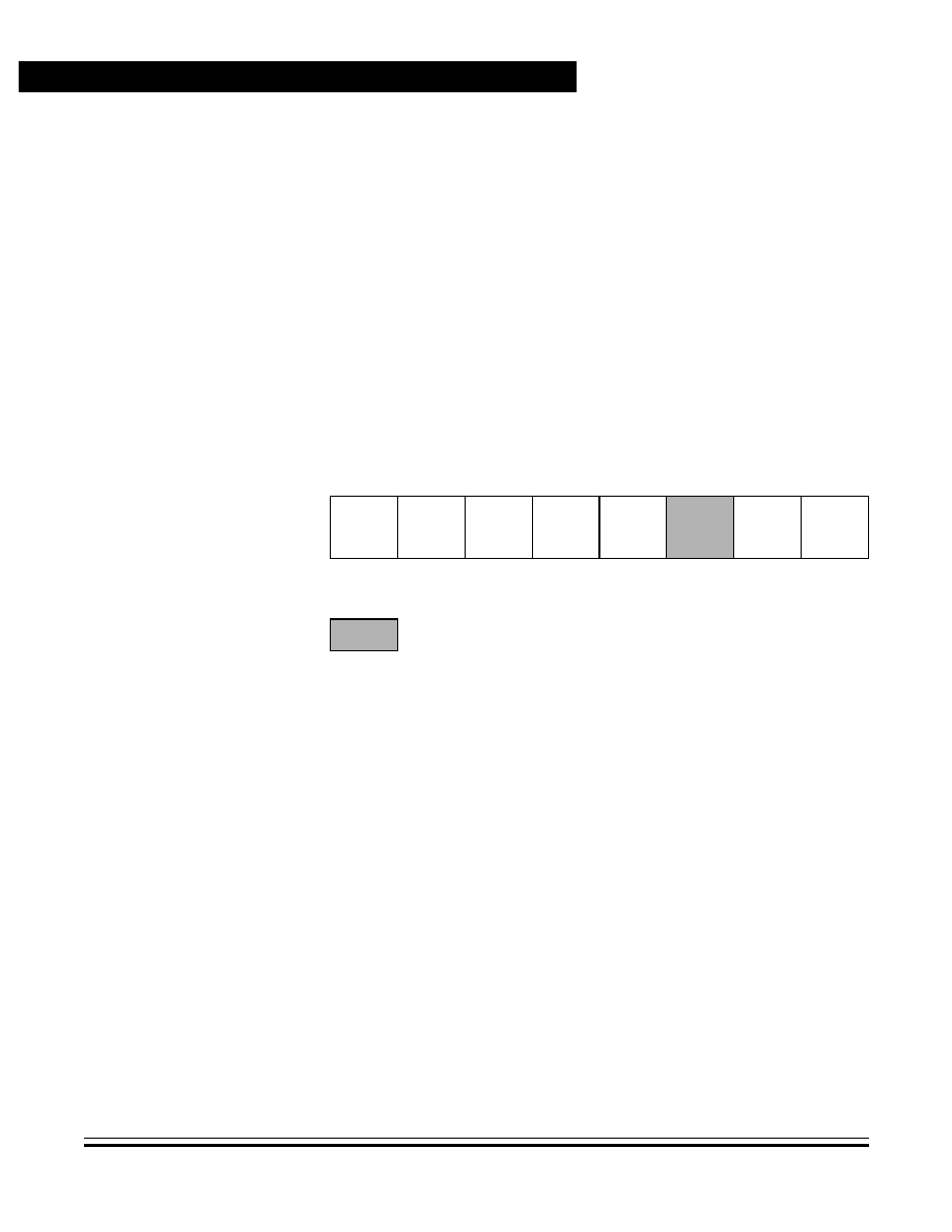
Technical Data
MC68HC705C8A -- Rev. 3
116
EPROM/OTPROM (PROM)
MOTOROLA
EPROM/OTPROM (PROM)
9.5 Control Registers
This subsection describes the three registers that control memory
configuration, PROM security, and IRQ edge or level sensitivity; port B
pullups; and non-programmable COP enable/disable.
9.5.1 Option Register
The option register shown in
Figure 9-4
is used to select the IRQ
sensitivity, enable the PROM security, and select the memory
configuration.
RAM0 -- Random-Access Memory Control Bit 0
1 = Maps 32 bytes of RAM into page zero starting at address
$0030. Addresses from $0020 to $002F are reserved. This bit
can be read or written at any time, allowing memory
configuration to be changed during program execution.
0 = Provides 48 bytes of PROM at location $0020≠$005F.
RAM1 -- Random-Access Memory Control Bit 1
1 = Maps 96 bytes of RAM into page one starting at address $0100.
This bit can be read or written at any time, allowing memory
configuration to be changed during program execution.
0 = Provides 96 bytes of PROM at location $0100.
Address:
$1FDF
Bit 7
6
5
4
3
2
1
Bit 0
Read:
RAM0
RAM1
0
0
SEC
*
IRQ
0
Write:
Reset:
0
0
0
0
*
U
1
0
*
Implemented as an EPROM cell
= Unimplemented
U = Unaffected
Figure 9-4. Option Register (Option)

EPROM/OTPROM (PROM)
Control Registers
MC68HC705C8A -- Rev. 3
Technical Data
MOTOROLA
EPROM/OTPROM (PROM)
117
SEC -- Security Bit
This bit is implemented as an EPROM cell and is not affected by
reset.
1 = Security enabled
0 = Security off; bootloader able to be enabled
IRQ -- Interrupt Request Pin Sensitivity Bit
IRQ is set only by reset, but can be cleared by software. This bit can
only be written once.
1 = IRQ pin is both negative edge- and level-sensitive.
0 = IRQ pin is negative edge-sensitive only.
Bits 5, 4, and 0 -- Not used; always read 0
Bit 2 -- Unaffected by reset; reads either 1 or 0
9.5.2 Mask Option Register 1
Mask option register 1 (MOR1) shown in
Figure 9-5
is an EPROM
register that enables the port B pullup devices. Data from MOR1 is
latched on the rising edge of the voltage on the RESET pin.
See
4.3.3 Port B Interrupts
.
PBPU7≠PBPU0/COPC -- Port B Pullup Enable Bits 7≠0
These EPROM bits enable the port B pullup devices.
1 = Port B pullups enabled
0 = Port B pullups disabled
Address:
$1FF0
Bit 7
6
5
4
3
2
1
Bit 0
Read:
PBPU7
PBPU6
PBPU5
PBPU4
PBPU3
PBPU2
PBPU1
PBPU0/
COPC
Write:
Reset:
Unaffected by reset
Erased:
0
0
0
0
0
0
0
0
Figure 9-5. Mask Option Register 1 (MOR1)

Technical Data
MC68HC705C8A -- Rev. 3
118
EPROM/OTPROM (PROM)
MOTOROLA
EPROM/OTPROM (PROM)
NOTE:
PBPU0/COPC programmed to a 1 enables the port B pullup bit. This bit
is also used to clear the non-programmable COP (MC68HC05C4A
type). Writing to this bit to clear the COP will not affect the state of the
port B pull-up (bit 0). See
5.3.3 Programmable and
Non-Programmable COP Watchdog Resets
.
When using the MC68HC705C8A in an MC68HC705C8 or
MC68HSC705C8 application, program locations $1FF0 and $1FF1 to
$00.
9.5.3 Mask Option Register 2
Mask option register 2 (MOR2) shown in
Figure 9-6
is an EPROM
register that enables the non-programmable COP watchdog. Data from
MOR2 is latched on the rising edge of the voltage on the RESET pin.
See
5.3.3 Programmable and Non-Programmable COP Watchdog
Resets
.
NCOPE -- Non-Programmable COP Watchdog Enable Bit
This EPROM bit enables the non-programmable COP watchdog.
1 = Non-programmable COP watchdog enabled
0 = Non-programmable COP watchdog disabled
Address:
$1FF1
Bit 7
6
5
4
3
2
1
Bit 0
Read:
NCOPE
Write:
Reset:
Unaffected by reset
Erased:
0
0
0
0
0
0
0
0
= Unimplemented
Figure 9-6. Mask Option Register 2 (MOR2)

EPROM/OTPROM (PROM)
EPROM Erasing
MC68HC705C8A -- Rev. 3
Technical Data
MOTOROLA
EPROM/OTPROM (PROM)
119
9.6 EPROM Erasing
The erased state of an EPROM or OTPROM byte is $00. EPROM
devices can be erased by exposure to a high intensity ultraviolet (UV)
light with a wave length of 2537 ≈. The recommended erasure dosage
(UV intensity on a given surface area x exposure time) is 15 Ws/cm
2
. UV
lamps should be used without short-wave filters, and the EPROM device
should be positioned about one inch from the UV source.
OTPROM devices are shipped in an erased state. Once programmed,
they cannot be erased. Electrical erasing procedures cannot be
performed on either EPROM or OTPROM devices.

Technical Data
MC68HC705C8A -- Rev. 3
120
EPROM/OTPROM (PROM)
MOTOROLA
EPROM/OTPROM (PROM)

MC68HC705C8A -- Rev. 3
Technical Data
MOTOROLA
Serial Communications Interface (SCI)
121
Technical Data -- MC68HC705C8A
Section 10. Serial Communications Interface (SCI)
10.1 Contents
10.2
Introduction . . . . . . . . . . . . . . . . . . . . . . . . . . . . . . . . . . . . . . . 121
10.3
Features . . . . . . . . . . . . . . . . . . . . . . . . . . . . . . . . . . . . . . . . . 122
10.4
SCI Data Format. . . . . . . . . . . . . . . . . . . . . . . . . . . . . . . . . . . 122
10.5
SCI Operation . . . . . . . . . . . . . . . . . . . . . . . . . . . . . . . . . . . . .123
10.5.1
Transmitter . . . . . . . . . . . . . . . . . . . . . . . . . . . . . . . . . . . . .123
10.5.2
Receiver . . . . . . . . . . . . . . . . . . . . . . . . . . . . . . . . . . . . . . . 127
10.6
SCI I/O Registers . . . . . . . . . . . . . . . . . . . . . . . . . . . . . . . . . . 129
10.6.1
SCI Data Register . . . . . . . . . . . . . . . . . . . . . . . . . . . . . . . 129
10.6.2
SCI Control Register 1 . . . . . . . . . . . . . . . . . . . . . . . . . . . .130
10.6.3
SCI Control Register 2 . . . . . . . . . . . . . . . . . . . . . . . . . . . .131
10.6.4
SCI Status Register . . . . . . . . . . . . . . . . . . . . . . . . . . . . . . 133
10.6.5
Baud Rate Register . . . . . . . . . . . . . . . . . . . . . . . . . . . . . . 136
10.2 Introduction
The serial communications interface (SCI) module allows high-speed
asynchronous communication with peripheral devices and other
microcontroller units (MCUs).

Technical Data
MC68HC705C8A -- Rev. 3
122
Serial Communications Interface (SCI)
MOTOROLA
Serial Communications Interface (SCI)
10.3 Features
Features of the SCI module include:
∑
Standard mark/space non-return-to-zero format
∑
Full-duplex operation
∑
32 programmable baud rates
∑
Programmable 8-bit or 9-bit character length
∑
Separately enabled transmitter and receiver
∑
Two receiver wakeup methods:
≠
Idle line wakeup
≠
Address mark wakeup
∑
Interrupt-driven operation capability with five interrupt flags:
≠
Transmitter data register empty
≠
Transmission complete
≠
Receiver data register full
≠
Receiver overrun
≠
Idle receiver input
∑
Receiver framing error detection
∑
1/16 bit-time noise detection
10.4 SCI Data Format
The SCI uses the standard non-return-to-zero mark/space data format
illustrated in
Figure 10-1
.
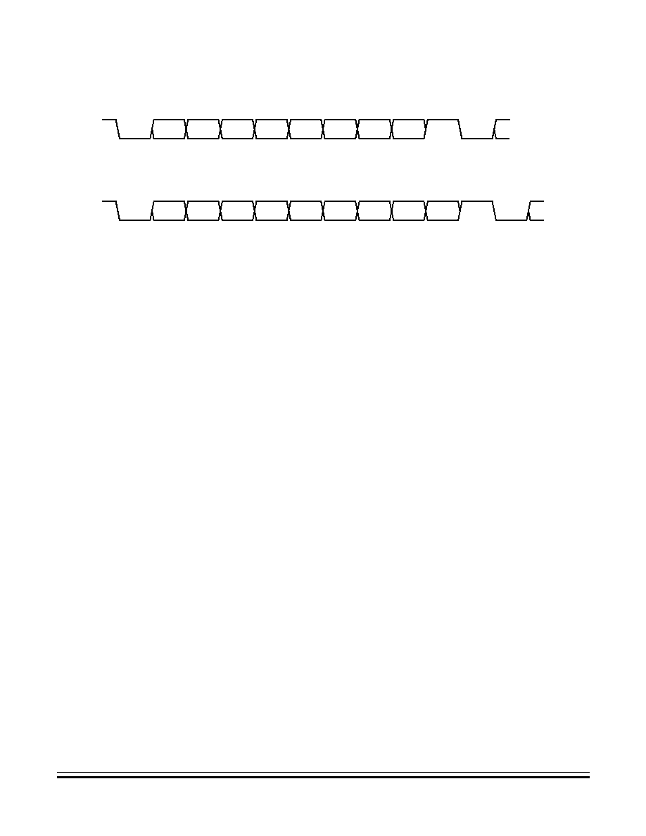
Serial Communications Interface (SCI)
SCI Operation
MC68HC705C8A -- Rev. 3
Technical Data
MOTOROLA
Serial Communications Interface (SCI)
123
Figure 10-1. SCI Data Format
10.5 SCI Operation
The SCI allows full-duplex, asynchronous, RS232 or RS422 serial
communication between the MCU and remote devices, including other
MCUs. The transmitter and receiver of the SCI operate independently,
although they use the same baud-rate generator. This subsection
describes the operation of the SCI transmitter and receiver.
10.5.1 Transmitter
Figure 10-2
shows the structure of the SCI transmitter.
Figure 10-3
is a
summary of the SCI transmitter input/output (I/O) registers.
∑
Character Length -- The transmitter can accommodate either
8-bit or 9-bit data. The state of the M bit in SCI control register 1
(SCCR1) determines character length. When transmitting 9-bit
data, bit T8 in SCCR1 is the ninth bit (bit 8).
∑
Character Transmission -- During transmission, the transmit shift
register shifts a character out to the PD1/TDO pin. The SCI data
register (SCDR) is the write-only buffer between the internal data
bus and the transmit shift register.
8-BIT DATA FORMAT
(BIT M IN SCCR1 CLEAR)
9-BIT DATA FORMAT
(BIT M IN SCCR1 SET)
START
BIT
BIT 0
BIT 1
BIT 2
BIT 3
BIT 4
BIT 5
BIT 6
BIT 7
BIT 8
STOP
BIT
NEXT
START
BIT
BIT 0
BIT 1
BIT 2
BIT 3
BIT 4
BIT 5
BIT 6
BIT 7
START
BIT
STOP
BIT
NEXT
START
BIT

Technical Data
MC68HC705C8A -- Rev. 3
124
Serial Communications Interface (SCI)
MOTOROLA
Serial Communications Interface (SCI)
Figure 10-2. SCI Transmitter
SCDR ($0011)
TRANSMIT SHIFT REGISTER
7 6 5 4 3 2
1 0
8
H
L
TRANSMITTER
CONTROL LOGIC
LOAD
F
R
OM
SC
D
R
S
H
I
F
T
EN
AB
L
E
PR
EAM
BLE
(A
LL
LOGI
C
1s
)
BR
EAK
(A
LL
LOGI
C
0s
)
PIN BUFFER
AND CONTROL
PD1/
TDO
SCI RECEIVE
REQUESTS
SCI INTERRUPT
REQUEST
1X
BAUD RATE
CLOCK
SCCR1 ($000E)
SCCR2 ($000F)
SCSR ($0010)
TIE
TCI
E
RIE
IL
IE
TE
RE
RW
U
SB
K
TD
RE
TC
RDR
F
IDL
E
OR
NF
FE
R8
T8
M
WA
K
E
TIE
TDRE
TC
TCIE
INT
E
R
N
A
L
DA
T
A
B
U
S
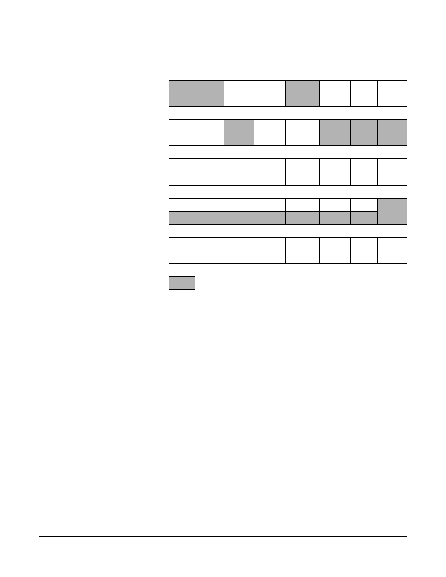
Serial Communications Interface (SCI)
SCI Operation
MC68HC705C8A -- Rev. 3
Technical Data
MOTOROLA
Serial Communications Interface (SCI)
125
Writing a logic 1 to the TE bit in SCI control register 2 (SCCR2) and
then writing data to the SCDR begins the transmission. At the start
of a transmission, transmitter control logic automatically loads the
transmit shift register with a preamble of logic 1s. After the
preamble shifts out, the control logic transfers the SCDR data into
the shift register. A logic 0 start bit automatically goes into the least
significant bit (LSB) position of the shift register, and a logic 1 stop
bit goes into the most significant bit (MSB) position.
When the data in the SCDR transfers to the transmit shift register,
the transmit data register empty (TDRE) flag in the SCI status
register (SCSR) becomes set. The TDRE flag indicates that the
SCDR can accept new data from the internal data bus.
When the shift register is not transmitting a character, the
PD1/TDO pin goes to the idle condition, logic 1. If software clears
the TE bit during the idle condition, and while TDRE is set, the
transmitter relinquishes control of the PD1/TDO pin.
Addr.
Register Name
Bit 7
6
5
4
3
2
1
Bit 0
$000D
Baud Rate Register
(Baud)
See page 136.
Read:
SCP1
SCP0
SCR2
SCR1
SCR0
Write:
Reset:
U
U
0
0
U
U
U
U
$000E
SCI Control Register 1
(SCCR1)
See page 130.
Read:
R8
T8
M
WAKE
Write:
Reset:
U
U
U
U
$000F
SCI Control Register 2
(SCCR2)
See page 131.
Read:
TIE
TCIE
RIE
ILIE
TE
RE
RWU
SBK
Write:
Reset:
0
0
0
0
0
0
0
0
$0010
SCI Status Register
(SCSR)
See page 133.
Read: TDRE
TC
RDRF
IDLE
OR
NF
FE
Write:
Reset:
1
1
0
0
0
0
0
U
$0011
SCI Data Register
(SCDR)
See page 129.
Read:
Bit 7
Bit 6
Bit 5
Bit 4
Bit 3
Bit 2
Bit 1
Bit 0
Write:
Reset:
Unaffected by reset
= Unimplemented
U = Unaffected
Figure 10-3. SCI Transmitter I/O Register Summary

Technical Data
MC68HC705C8A -- Rev. 3
126
Serial Communications Interface (SCI)
MOTOROLA
Serial Communications Interface (SCI)
∑
Break Characters -- Writing a logic 1 to the SBK bit in SCCR2
loads the shift register with a break character. A break character
contains all logic 0s and has no start and stop bits. Break
character length depends on the M bit in SCCR1. As long as SBK
is at logic 1, transmitter logic continuously loads break characters
into the shift register. After software clears the SBK bit, the shift
register finishes transmitting the last break character and then
transmits at least one logic 1. The automatic logic 1 at the end of
a break character is to guarantee the recognition of the start bit of
the next character.
∑
Idle Characters -- An idle character contains all logic 1s and has
no start or stop bits. Idle character length depends on the M bit in
SCCR1. The preamble is a synchronizing idle character that
begins every transmission.
Clearing the TE bit during a transmission relinquishes the
PD1/TDO pin after the last character to be transmitted is shifted
out. The last character may already be in the shift register, or
waiting in the SCDR, or it may be a break character generated by
writing to the SBK bit. Toggling TE from logic 0 to logic 1 while the
last character is in transmission generates an idle character (a
preamble) that allows the receiver to maintain control of the
PD1/TDO pin.
∑
Transmitter Interrupts -- These sources can generate SCI
transmitter interrupt requests:
≠
Transmit Data Register Empty (TDRE) -- The TDRE bit in the
SCSR indicates that the SCDR has transferred a character to
the transmit shift register. TDRE is a source of SCI interrupt
requests. The transmission complete interrupt enable bit
(TCIE) in SCCR2 is the local mask for TDRE interrupts.
≠
Transmission Complete (TC) -- The TC bit in the SCSR
indicates that both the transmit shift register and the SCDR are
empty and that no break or idle character has been generated.
TC is a source of SCI interrupt requests. The transmission
complete interrupt enable bit (TCIE) in SCCR2 is the local
mask for TC interrupts.
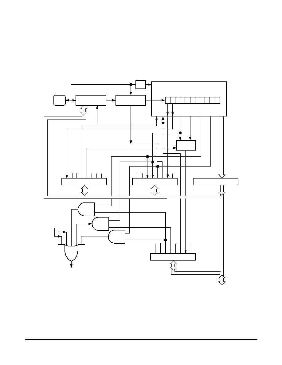
Serial Communications Interface (SCI)
SCI Operation
MC68HC705C8A -- Rev. 3
Technical Data
MOTOROLA
Serial Communications Interface (SCI)
127
10.5.2 Receiver
Figure 10-4
shows the structure of the SCI receiver. Refer to
Figure 10-3
for a summary of the SCI receiver I/O registers.
Figure 10-4. SCI Receiver
RECEIVE SHIFT REGISTER
7 6 5 4 3 2 1 0
8
PIN BUFFER
AND CONTROL
PD0/
RDI
16X
BAUD RATE
CLOCK
DATA
RECOVERY
ST
O
P
ST
AR
T
˜
16
IDLE
WAKEUP
LOGIC
SCSR ($0010)
TDRE
TC
RDR
F
IDL
E
OR
NF
FE
SCDR ($0011)
SCCR1 ($000E)
R8
T8
M
WA
K
E
SCCR2 ($000F)
TI
E
TC
I
E
RI
E
IL
I
E
TE
RE
RW
U
SBK
MSB RDRF OR
RDRF
RIE
IDLE
ILIE
OR
RIE
SCI TRANSMIT
REQUESTS
SCI INTERRUPT
REQUEST
I
N
TE
RN
A
L
DA
T
A
B
U
S
RE
M
DISABLE
DRIVER
IN
TE
RNA
L
D
A
T
A
B
U
S

Technical Data
MC68HC705C8A -- Rev. 3
128
Serial Communications Interface (SCI)
MOTOROLA
Serial Communications Interface (SCI)
∑
Character Length -- The receiver can accommodate either 8-bit
or 9-bit data. The state of the M bit in SCI control register 1
(SCCR1) determines character length. When receiving 9-bit data,
bit R8 in SCCR1 is the ninth bit (bit 8).
∑
Character Reception -- During reception, the receive shift register
shifts characters in from the PD0/RDI pin. The SCI data register
(SCDR) is the read-only buffer between the internal data bus and
the receive shift register.
After a complete character shifts into the receive shift register, the
data portion of the character is transferred to the SCDR, setting
the receive data register full (RDRF) flag. The RDRF flag can be
used to generate an interrupt.
∑
Receiver Wakeup -- So that the MCU can ignore transmissions
intended only for other receivers in multiple-receiver systems, the
MCU can be put into a standby state. Setting the receiver wakeup
enable (RWU) bit in SCI control register 2 (SCCR2) puts the MCU
into a standby state during which receiver interrupts are disabled.
Either of two conditions on the PD0/RDI pin can bring the MCU out
of the standby state:
≠
Idle input line condition -- If the PD0/RDI pin is at logic 1 long
enough for 10 or 11 logic 1s to shift into the receive shift
register, receiver interrupts are again enabled.
≠
Address mark -- If a logic 1 occurs in the most significant bit
position of a received character, receiver interrupts are again
enabled.
The state of the WAKE bit in SCCR1 determines which of the two
conditions wakes up the MCU.
∑
Receiver Noise Immunity -- The data recovery logic samples
each bit 16 times to identify and verify the start bit and to detect
noise. Any conflict between noise detection samples sets the
noise flag (NF) in the SCSR. The NF bit is set at the same time
that the RDRF bit is set.

Serial Communications Interface (SCI)
SCI I/O Registers
MC68HC705C8A -- Rev. 3
Technical Data
MOTOROLA
Serial Communications Interface (SCI)
129
∑
Framing Errors -- If the data recovery logic does not detect a logic
1 where the stop bit should be in an incoming character, it sets the
framing error (FE) bit in the SCSR. The FE bit is set at the same
time that the RDRF bit is set.
∑
Receiver Interrupts -- These sources can generate SCI receiver
interrupt requests:
≠
Receive Data Register Full (RDRF) -- The RDRF bit in the
SCSR indicates that the receive shift register has transferred a
character to the SCDR.
≠
Receiver Overrun (OR) -- The OR bit in the SCSR indicates
that the receive shift register shifted in a new character before
the previous character was read from the SCDR.
≠
Idle Input (IDLE) -- The IDLE bit in the SCSR indicates that 10
or 11 consecutive logic 1s shifted in from the PD0/RDI pin.
10.6 SCI I/O Registers
These I/O registers control and monitor SCI operation:
∑
SCI data register (SCDR)
∑
SCI control register 1 (SCCR1)
∑
SCI control register 2 (SCCR2)
∑
SCI status register (SCSR)
10.6.1 SCI Data Register
The SCI data register (SCDR) shown in
Figure 10-5
is the buffer for
characters received and for characters transmitted.
Address:
$0011
Bit 7
6
5
4
3
2
1
Bit 0
Read:
Bit 7
Bit 6
Bit 5
Bit 4
Bit 3
Bit 2
Bit 1
Bit 0
Write:
Reset:
Unaffected by reset
Figure 10-5. SCI Data Register (SCDR)

Technical Data
MC68HC705C8A -- Rev. 3
130
Serial Communications Interface (SCI)
MOTOROLA
Serial Communications Interface (SCI)
10.6.2 SCI Control Register 1
SCI control register 1 (SCCR1) shown in
Figure 10-6
has these
functions:
∑
Stores ninth SCI data bit received and ninth SCI data bit
transmitted
∑
Controls SCI character length
∑
Controls SCI wakeup method
R8 -- Bit 8 (Received)
When the SCI is receiving 9-bit characters, R8 is the ninth bit of the
received character. R8 receives the ninth bit at the same time that the
SCDR receives the other eight bits. Reset has no effect on the R8 bit.
T8 -- Bit 8 (Transmitted)
When the SCI is transmitting 9-bit characters, T8 is the ninth bit of the
transmitted character. T8 is loaded into the transmit shift register at
the same time that SCDR is loaded into the transmit shift register.
Reset has no effect on the T8 bit.
M -- Character Length Bit
This read/write bit determines whether SCI characters are eight or
nine bits long. The ninth bit can be used as an extra stop bit, as a
receiver wakeup signal, or as a mark or space parity bit. Reset has no
effect on the M bit.
1 = 9-bit SCI characters
0 = 8-bit SCI characters
Address:
$000E
Bit 7
6
5
4
3
2
1
Bit 0
Read:
R8
T8
M
WAKE
Write:
Reset:
U
U
U
U
= Unimplemented
U = Unaffected
Figure 10-6. SCI Control Register 1 (SCCR1)

Serial Communications Interface (SCI)
SCI I/O Registers
MC68HC705C8A -- Rev. 3
Technical Data
MOTOROLA
Serial Communications Interface (SCI)
131
WAKE -- Wakeup Bit
This read/write bit determines which condition wakes up the SCI: a
logic 1 (address mark) in the most significant bit position of a received
character or an idle condition of the PD0/RDI pin. Reset has no effect
on the WAKE bit.
1 = Address mark wakeup
0 = Idle line wakeup
10.6.3 SCI Control Register 2
SCI control register 2 (SCCR2) shown in
Figure 10-7
has these
functions:
∑
Enables the SCI receiver and SCI receiver interrupts
∑
Enables the SCI transmitter and SCI transmitter interrupts
∑
Enables SCI receiver idle interrupts
∑
Enables SCI transmission complete interrupts
∑
Enables SCI wakeup
∑
Transmits SCI break characters
TIE -- Transmit Interrupt Enable Bit
This read/write bit enables SCI interrupt requests when the TDRE bit
becomes set. Reset clears the TIE bit.
1 = TDRE interrupt requests enabled
0 = TDRE interrupt requests disabled
Address:
$000F
Bit 7
6
5
4
3
2
1
Bit 0
Read:
TIE
TCIE
RIE
ILIE
TE
RE
RWU
SBK
Write:
Reset:
0
0
0
0
0
0
0
0
Figure 10-7. SCI Control Register 2 (SCCR2)

Technical Data
MC68HC705C8A -- Rev. 3
132
Serial Communications Interface (SCI)
MOTOROLA
Serial Communications Interface (SCI)
TCIE -- Transmission Complete Interrupt Enable Bit
This read/write bit enables SCI interrupt requests when the TC bit
becomes set. Reset clears the TCIE bit.
1 = TC interrupt requests enabled
0 = TC interrupt requests disabled
RIE -- Receive Interrupt Enable Bit
This read/write bit enables SCI interrupt requests when the RDRF bit
or the OR bit becomes set. Reset clears the RIE bit.
1 = RDRF interrupt requests enabled
0 = RDRF interrupt requests disabled
ILIE -- Idle Line Interrupt Enable Bit
This read/write bit enables SCI interrupt requests when the IDLE bit
becomes set. Reset clears the ILIE bit.
1 = IDLE interrupt requests enabled
0 = IDLE interrupt requests disabled
TE -- Transmit Enable Bit
Setting this read/write bit begins the transmission by sending a
preamble of 10 or 11 logic 1s from the transmit shift register to the
PD1/TDO pin. Reset clears the TE bit.
1 = Transmission enabled
0 = Transmission disabled
RE -- Receive Enable Bit
Setting this read/write bit enables the receiver. Clearing the RE bit
disables the receiver and receiver interrupts but does not affect the
receiver interrupt flags. Reset clears the RE bit.
1 = Receiver enabled
0 = Receiver disabled
RWU -- Receiver Wakeup Enable Bit
This read/write bit puts the receiver in a standby state. Typically, data
transmitted to the receiver clears the RWU bit and returns the receiver
to normal operation. The WAKE bit in SCCR1 determines whether an

Serial Communications Interface (SCI)
SCI I/O Registers
MC68HC705C8A -- Rev. 3
Technical Data
MOTOROLA
Serial Communications Interface (SCI)
133
idle input or an address mark brings the receiver out of the standby
state. Reset clears the RWU bit.
1 = Standby state
0 = Normal operation
SBK -- Send Break Bit
Setting this read/write bit continuously transmits break codes in the
form of 10-bit or 11-bit groups of logic 0s. Clearing the SBK bit stops
the break codes and transmits a logic 1 as a start bit. Reset clears the
SBK bit.
1 = Break codes being transmitted
0 = No break codes being transmitted
10.6.4 SCI Status Register
The SCI status register (SCSR) shown in
Figure 10-8
contains flags to
signal these conditions:
∑
Transfer of SCDR data to transmit shift register complete
∑
Transmission complete
∑
Transfer of receive shift register data to SCDR complete
∑
Receiver input idle
∑
Receiver overrun
∑
Noisy data
∑
Framing error
Address:
$0010
Bit 7
6
5
4
3
2
1
Bit 0
Read:
TDRE
TC
RDRF
IDLE
OR
NF
FE
Write:
Reset:
1
1
0
0
0
0
0
U
= Unimplemented
U = Unaffected
Figure 10-8. SCI Status Register (SCSR)

Technical Data
MC68HC705C8A -- Rev. 3
134
Serial Communications Interface (SCI)
MOTOROLA
Serial Communications Interface (SCI)
TDRE -- Transmit Data Register Empty Bit
This clearable, read-only bit is set when the data in the SCDR
transfers to the transmit shift register. TDRE generates an interrupt
request if the TIE bit in SCCR2 is also set. Clear the TDRE bit by
reading the SCSR with TDRE set and then writing to the SCDR. Reset
sets the TDRE bit. Software must initialize the TDRE bit to logic 0 to
avoid an instant interrupt request when turning on the transmitter.
1 = SCDR data transferred to transmit shift register
0 = SCDR data not transferred to transmit shift register
TC -- Transmission Complete Bit
This clearable, read-only bit is set when the TDRE bit is set and no
data, preamble, or break character is being transmitted. TC generates
an interrupt request if the TCIE bit in SCCR2 is also set. Clear the TC
bit by reading the SCSR with TC set and then writing to the SCDR.
Reset sets the TC bit. Software must initialize the TC bit to logic 0 to
avoid an instant interrupt request when turning on the transmitter.
1 = No transmission in progress
0 = Transmission in progress
RDRF -- Receive Data Register Full Bit
This clearable, read-only bit is set when the data in the receive shift
register transfers to the SCI data register. RDRF generates an
interrupt request if the RIE bit in SCCR2 is also set. Clear the RDRF
bit by reading the SCSR with RDRF set and then reading the SCDR.
Reset clears the RDRF bit.
1 = Received data available in SCDR
0 = Received data not available in SCDR
IDLE -- Receiver Idle Bit
This clearable, read-only bit is set when 10 or 11 consecutive logic 1s
appear on the receiver input. IDLE generates an interrupt request if
the ILIE bit in SCCR2 is also set. Clear the IDLE bit by reading the
SCSR with IDLE set, and then reading the SCDR. Reset clears the
IDLE bit.
1 = Receiver input idle
0 = Receiver input not idle

Serial Communications Interface (SCI)
SCI I/O Registers
MC68HC705C8A -- Rev. 3
Technical Data
MOTOROLA
Serial Communications Interface (SCI)
135
OR -- Receiver Overrun Bit
This clearable, read-only bit is set if the SCDR is not read before the
receive shift register receives the next word. OR generates an
interrupt request if the RIE bit in SCCR2 is also set. The data in the
shift register is lost, but the data already in the SCDR is not affected.
Clear the OR bit by reading the SCSR with OR set and then reading
the SCDR. Reset clears the OR bit.
1 = Receiver shift register full and RDRF = 1
0 = No receiver overrun
NF -- Receiver Noise Flag Bit
This clearable, read-only bit is set when noise is detected in data
received in the SCI data register. Clear the NF bit by reading the
SCSR and then reading the SCDR. Reset clears the NF bit.
1 = Noise detected in SCDR
0 = No noise detected in SCDR
FE -- Receiver Framing Error Bit
This clearable, read-only flag is set when a logic 0 is located where a
stop bit should be in the character shifted into the receive shift
register. If the received word causes both a framing error and an
overrun error, the OR bit is set and the FE bit is not set. Clear the FE
bit by reading the SCSR and then reading the SCDR. Reset clears the
FE bit.
1 = Framing error
0 = No framing error

Technical Data
MC68HC705C8A -- Rev. 3
136
Serial Communications Interface (SCI)
MOTOROLA
Serial Communications Interface (SCI)
10.6.5 Baud Rate Register
The baud rate register shown in
Figure 10-9
selects the baud rate for
both the receiver and the transmitter.
SCP1 and SCP0 -- SCI Prescaler Select Bits
These read/write bits control prescaling of the baud rate generator
clock, as shown in
Table 10-1
. Resets clear both SCP1 and SCP0.
Address:
$000D
Bit 7
6
5
4
3
2
1
Bit 0
Read:
SCP1
SCP0
SCR2
SCR1
SCR0
Write:
Reset:
U
U
0
0
U
U
U
U
= Unimplemented
U = Unaffected
Figure 10-9. Baud Rate Register (Baud)
Table 10-1. Baud Rate Generator Clock Prescaling
SCP[1:0]
Baud Rate Generator Clock
00
Internal clock
˜
1
01
Internal clock
˜
3
10
Internal clock
˜
4
11
Internal clock
˜
13
Serial Communications Interface (SCI)
SCI I/O Registers
MC68HC705C8A -- Rev. 3
Technical Data
MOTOROLA
Serial Communications Interface (SCI)
137
SCR2≠SCR0 -- SCI Baud Rate Select Bits
These read/write bits select the SCI baud rate, as shown in
Table 10-2
. Reset has no effect on the SCR2≠SCR0 bits.
Table 10-3
shows all possible SCI baud rates derived from crystal
frequencies of 2 MHz, 4 MHz, and 4.194304 MHz.
Table 10-2. Baud Rate Selection
SCR[2:1:0]
SCI Baud Rate (Baud)
000
Prescaled clock
˜
1
001
Prescaled clock
˜
2
010
Prescaled clock
˜
4
011
Prescaled clock
˜
8
100
Prescaled clock
˜
16
101
Prescaled clock
˜
32
110
Prescaled clock
˜
64
111
Prescaled clock
˜
128

Technical Data
MC68HC705C8A -- Rev. 3
138
Serial Communications Interface (SCI)
MOTOROLA
Serial Communications Interface (SCI)
Table 10-3. Baud Rate Selection Examples
SCP[1:0]
SCR[2:1:0]
SCI Baud Rate
f
OSC
= 2 MHz
f
OSC
= 4 MHz
f
OSC
= 4.194304 MHz
00
000
62.50 Kbaud
125 Kbaud
131.1 Kbaud
00
001
31.25 Kbaud
62.50 Kbaud
65.54 Kbaud
00
010
15.63 Kbaud
31.25 Kbaud
32.77 Kbaud
00
011
7813 baud
15.63 Kbaud
16.38 Kbaud
00
100
3906 baud
7813 baud
8192 baud
00
101
1953 baud
3906 baud
4096 baud
00
110
976.6 baud
1953 baud
2048 baud
00
111
488.3 baud
976.6 baud
1024 baud
01
000
20.83 Kbaud
41.67 Kbaud
43.69 Kbaud
01
001
10.42 Kbaud
20.83 Kbaud
21.85 Kbaud
01
010
5208 baud
10.42 Kbaud
10.92 Kbaud
01
011
2604 baud
5208 baud
5461 baud
01
100
1302 baud
2604 baud
2731 baud
01
101
651.0 baud
1302 baud
1365 baud
01
110
325.5 baud
651.0 baud
682.7 baud
01
111
162.8 baud
325.5 baud
341.3 baud
10
000
15.63 Kbaud
31.25 Kbaud
32.77 Kbaud
10
001
7813 baud
15.63 Kbaud
16.38 Kbaud
10
010
3906 baud
7813 baud
8192 baud
10
011
1953 baud
3906 baud
4906 baud
10
100
976.6 baud
1953 baud
2048 baud
10
101
488.3 baud
976.6 baud
1024 baud
10
110
244.1 baud
488.3 baud
512.0 baud
10
111
122.1 baud
244.1 baud
256.0 baud
11
000
4808 baud
9615 baud
10.08 Kbaud
11
001
2404 baud
4808 baud
5041 baud
11
010
1202 baud
2404 baud
2521 baud
11
011
601.0 baud
1202 baud
1260 baud
11
100
300.5 baud
601.0 baud
630.2 baud
11
101
150.2 baud
300.5 baud
315.1 baud
11
110
75.12 baud
150.2 baud
157.5 baud
11
111
37.56 baud
75.12 baud
78.77 baud

MC68HC705C8A -- Rev. 3
Technical Data
MOTOROLA
Serial Peripheral Interface (SPI)
139
Technical Data -- MC68HC705C8A
Section 11. Serial Peripheral Interface (SPI)
11.1 Contents
11.2
Introduction . . . . . . . . . . . . . . . . . . . . . . . . . . . . . . . . . . . . . . . 139
11.3
Features . . . . . . . . . . . . . . . . . . . . . . . . . . . . . . . . . . . . . . . . . 140
11.4
Operation . . . . . . . . . . . . . . . . . . . . . . . . . . . . . . . . . . . . . . . . 142
11.4.1
Pin Functions in Master Mode . . . . . . . . . . . . . . . . . . . . . . 143
11.4.2
Pin Functions in Slave Mode . . . . . . . . . . . . . . . . . . . . . . .144
11.5
Multiple-SPI Systems . . . . . . . . . . . . . . . . . . . . . . . . . . . . . . . 145
11.6
Serial Clock Polarity and Phase . . . . . . . . . . . . . . . . . . . . . . .146
11.7
SPI Error Conditions . . . . . . . . . . . . . . . . . . . . . . . . . . . . . . . . 147
11.7.1
Mode Fault Error . . . . . . . . . . . . . . . . . . . . . . . . . . . . . . . .147
11.7.2
Write Collision Error . . . . . . . . . . . . . . . . . . . . . . . . . . . . . . 147
11.7.3
Overrun Error . . . . . . . . . . . . . . . . . . . . . . . . . . . . . . . . . . . 148
11.8
SPI Interrupts . . . . . . . . . . . . . . . . . . . . . . . . . . . . . . . . . . . . .148
11.9
SPI I/O Registers . . . . . . . . . . . . . . . . . . . . . . . . . . . . . . . . . . 148
11.9.1
SPI Data Register. . . . . . . . . . . . . . . . . . . . . . . . . . . . . . . . 149
11.9.2
SPI Control Register. . . . . . . . . . . . . . . . . . . . . . . . . . . . . . 149
11.9.3
SPI Status Register . . . . . . . . . . . . . . . . . . . . . . . . . . . . . . 151
11.2 Introduction
The serial peripheral interface (SPI) module allows full-duplex,
synchronous, serial communication with peripheral devices.

Technical Data
MC68HC705C8A -- Rev. 3
140
Serial Peripheral Interface (SPI)
MOTOROLA
Serial Peripheral Interface (SPI)
11.3 Features
Features of the SPI include:
∑
Full-duplex operation
∑
Master and slave modes
∑
Four programmable master mode frequencies (1.05 MHz
maximum)
∑
2.1-MHz maximum slave mode frequency
∑
Serial clock with programmable polarity and phase
∑
End of transmission interrupt flag
∑
Write collision error flag
∑
Bus contention error flag
Figure 11-1
shows the structure of the SPI module.
Figure 11-2
is a
summary of the SPI input/output (I/O) registers.
Serial Peripheral Interface (SPI)
Features
MC68HC705C8A -- Rev. 3
Technical Data
MOTOROLA
Serial Peripheral Interface (SPI)
141
Figure 11-1. SPI Block Diagram
SPI SHIFT REGISTER
DIVIDER
SPCR ($000A)
7 6 5 4 3 2 1
0
PD4/
SCK
PD3/
MOSI
˜
2
˜
32
˜
6
˜
4
SELECT
SPI CONTROL
S
M
M
S
INTERNAL
CLOCK
(XTAL
˜
2)
P
I
N
CO
NT
R
O
L
L
O
G
I
C
PD2/
MISO
SPSR ($000B)
SP
I
F
WC
O
L
MO
DF
REQUEST
SPR
1
SP
R
0
SPDR ($000C)
SPI INTERRUPT
INTERNAL
DATA BUS
SPI CLOCK (MASTER)
CLOCK
LOGIC
MSTR
SPE
M
S
MSTR
SPE
DWOM
SPI
E
SPE
DW
O
M
MS
T
R
CP
H
A
CP
O
L
SPR
1
SPR
0
SHIFT
CLOCK
SPIE
PD5/
SS
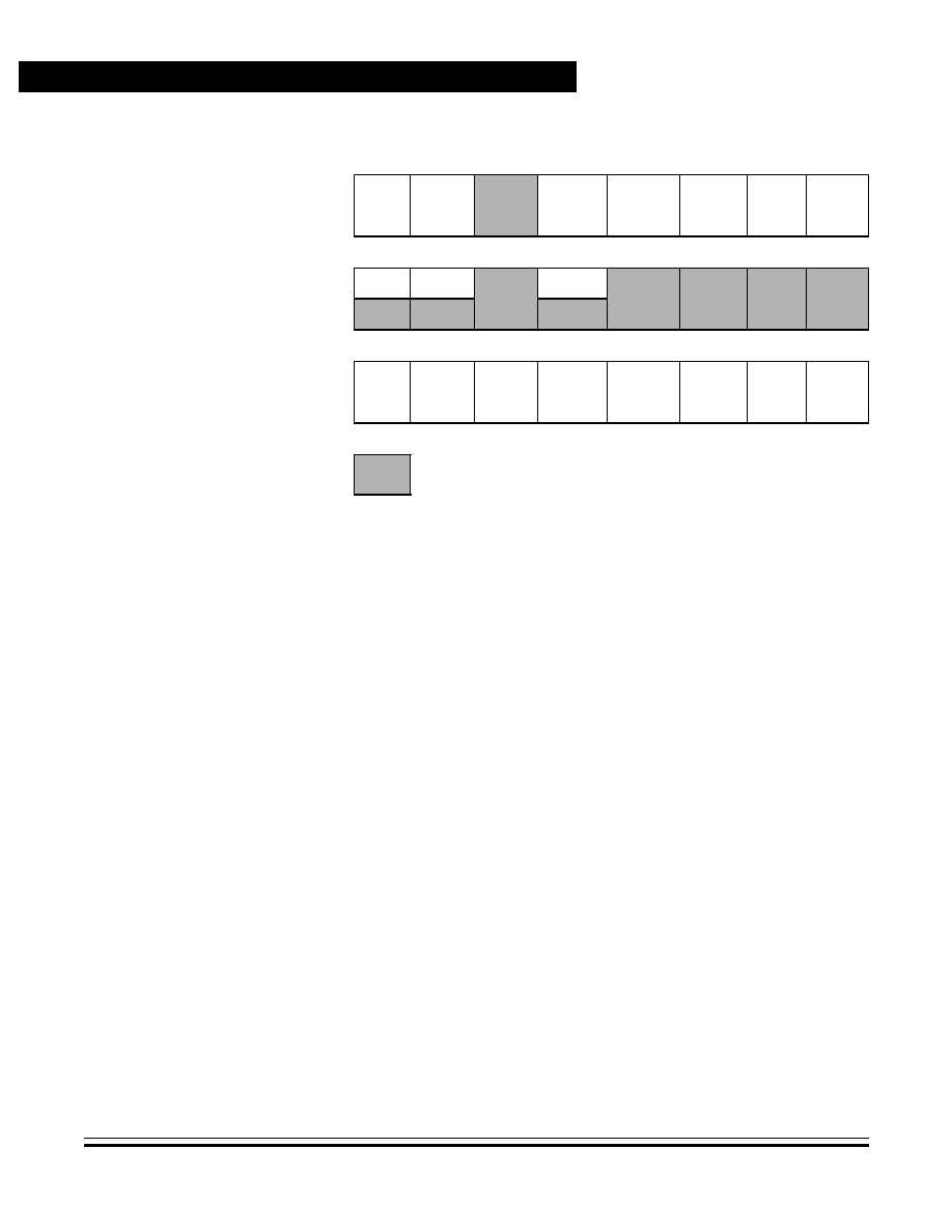
Technical Data
MC68HC705C8A -- Rev. 3
142
Serial Peripheral Interface (SPI)
MOTOROLA
Serial Peripheral Interface (SPI)
11.4 Operation
The master/slave SPI allows full-duplex, synchronous, serial
communication between the microcontroller unit (MCU) and peripheral
devices, including other MCUs. As the 8-bit shift register of a master SPI
transmits each byte to another device, a byte from the receiving device
enters the master SPI shift register. A clock signal from the master SPI
synchronizes data transmission.
Only a master SPI can initiate transmissions. Software begins the
transmission from a master SPI by writing to the SPI data register
(SPDR). The SPDR does not buffer data being transmitted from the SPI.
Data written to the SPDR goes directly into the shift register and begins
the transmission immediately under the control of the serial clock. The
transmission ends after eight cycles of the serial clock when the SPI flag
(SPIF) becomes set. At the same time that SPIF becomes set, the data
shifted into the master SPI from the receiving device transfers to the
SPDR. The SPDR buffers data being received by the SPI. Before the
master SPI sends the next byte, software must clear the SPIF bit by
reading the SPSR and then accessing the SPDR.
Addr.
Register Name
Bit 7
6
5
4
3
2
1
Bit 0
$000A
SPI Control Register
(SPCR)
See page 149.
Read:
SPIE
SPE
MSTR
CPOL
CPHA
SPR1
SPR0
Write:
Reset:
0
0
0
U
U
U
U
$000B
SPI Status Register
(SPSR)
See page 151.
Read:
SPIF
WCOL
MODF
Write:
Reset:
0
0
0
$000C
SPI Data Register
(SPDR)
See page 149.
Read:
Bit 7
Bit 6
Bit 5
Bit 4
Bit 3
BIt 2
Bit 1
Bit 0
Write:
Reset:
Unaffected by reset
= Unimplemented
U = Unaffected
Figure 11-2. SPI I/O Register Summary

Serial Peripheral Interface (SPI)
Operation
MC68HC705C8A -- Rev. 3
Technical Data
MOTOROLA
Serial Peripheral Interface (SPI)
143
In a slave SPI, data enters the shift register under the control of the serial
clock from the master SPI. After a byte enters the shift register of a slave
SPI, it transfers to the SPDR. To prevent an overrun condition, slave
software must then read the byte in the SPDR before another byte enters
the shift register and is ready to transfer to the SPDR.
Figure 11-3
shows how a master SPI exchanges data with a slave SPI.
Figure 11-3. Master/Slave Connections
11.4.1 Pin Functions in Master Mode
Setting the MSTR bit in the SPI control register (SPCR) configures the
SPI for operation in master mode. The master-mode functions of the SPI
pins are:
∑
PD4/SCK (serial clock) -- In master mode, the PD4/SCK pin is the
synchronizing clock output.
∑
PD3/MOSI (master output, slave input) -- In master mode, the
PD3/MOSI pin is the serial output.
∑
PD2/MISO (master input, slave output) -- In master mode, the
PD2/MISO pin is configured as the serial input.
∑
PD5/SS (slave select) -- In master mode, the PD5/SS pin protects
against driver contention caused by the simultaneous operation of
two SPIs in master mode. A logic 0 on the PD5/SS pin of a master
SPI disables the SPI, clears the MSTR bit, and sets the mode-fault
flag (MODF).
SPI SHIFT REGISTER
7 6 5 4 3 2 1 0
SPI SHIFT REGISTER
7 6 5 4 3 2 1 0
SPDR ($000C)
SPDR ($000C)
PD3/MOSI
PD2/MISO
PD5/SS
PD4/SCK
MASTER MCU
SLAVE MCU

Technical Data
MC68HC705C8A -- Rev. 3
144
Serial Peripheral Interface (SPI)
MOTOROLA
Serial Peripheral Interface (SPI)
11.4.2 Pin Functions in Slave Mode
Clearing the MSTR bit in the SPCR configures the SPI for operation in
slave mode. The slave-mode functions of the SPI pins are:
∑
PD4/SCK (serial clock) -- In slave mode, the PD4/SCK pin is the
input for the synchronizing clock signal from the master SPI.
∑
PD3/MOSI (master output, slave input) -- In slave mode, the
PD3/MOSI pin is the serial input.
∑
PD2/MISO (master input, slave output) -- In slave mode, the
PD2/MISO pin is the serial output.
∑
PD5/SS (slave select) -- In slave mode, the PD5/SS pin enables
the SPI for data and serial clock reception from a master SPI.
When CPHA = 0, the shift clock is the OR of SS with SCK. In this clock
phase mode, SS must go high between successive characters in an SPI
message. When CPHA = 1, SS may be left low for several SPI
characters. In cases with only one SPI slave MCU, the slave MCU SS
line can be tied to V
SS
as long as CPHA = 1 clock modes are used.
The WCOL flag bit can be improperly set when attempting the first
transmission after a reset if these conditions are present: MSTR = 0,
CPOL = 0, CPHA = 1, SS pin = 0, and SCK pin = 1. The reset states of
the CPOL and CPHA bits are 0 and 1, respectively. Under normal
operating conditions (CPOL = 0, CPHA = 1), the SCK input will be low.
The incorrect setting of the WCOL bit can be prevented in two ways:
1. Send a dummy transmission after reset, clear the WCOL flag, and
then proceed with the real transmission.
2. Use the MSTR bit in the SPCR (SPI control register). This is
accomplished by setting the MSTR bit at the same time the CPOL
and CPHA bits are programmed to the desired logic levels. Then,
the data register can be written to if desired. After this, the MSTR
bit should be set to a logic 0, the SPE (SPI enable bit) should be
set to a logic 1, and the CPOL, CPHA, SPR1, and SPR0 bits set
to the desired logic levels. If this procedure is followed after a reset
and before the first access to the SPDR, the WCOL flag will not be
set.
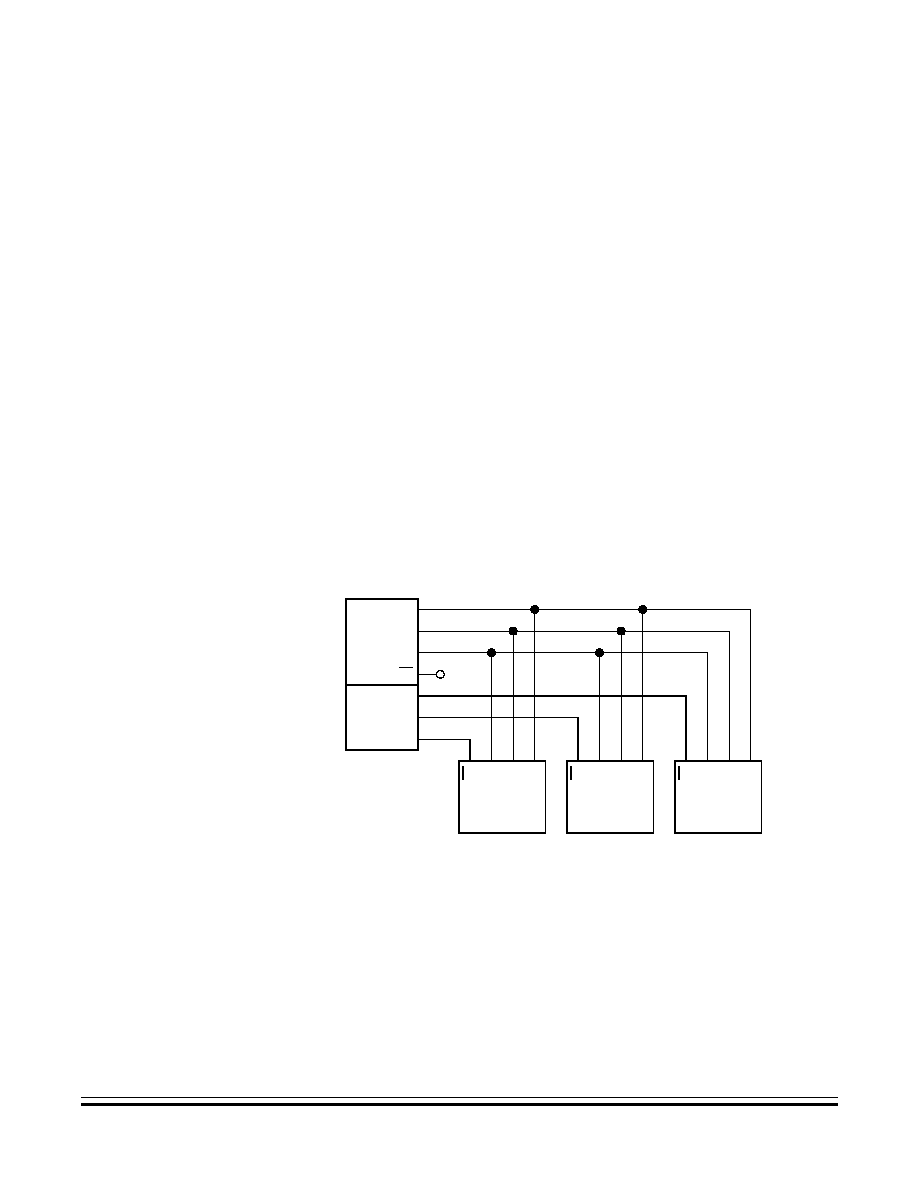
Serial Peripheral Interface (SPI)
Multiple-SPI Systems
MC68HC705C8A -- Rev. 3
Technical Data
MOTOROLA
Serial Peripheral Interface (SPI)
145
Example:
LDA #$1C
; MSTR = 1, CPOL = 1, CPHA = 1,
; SPR1 = SPR0 = 0
STA SPCR
; SPI control register
LDA #$4C
; MSTR = 0, SPE = 1, CPOL = 1, CPHA = 1,
; SPR1 = SPR0 = 0
STA SPCR
; SPI control register
11.5 Multiple-SPI Systems
In a multiple-SPI system, all PD4/SCK pins are connected together, all
PD3/MOSI pins are connected together, and all PD2/MISO pins are
connected together.
Before a transmission, one SPI is configured as master and the rest are
configured as slaves.
Figure 11-4
is a block diagram showing a single
master SPI and three slave SPIs.
Figure 11-4. One Master and Three Slaves Block Diagram
Figure 11-5
is another block diagram with two master/slave SPIs and
three slave SPIs.
PD2/MISO
PD3/MOSI
PD4/SCK
PD5/SS
I/O
2
1
0
SLAVE MCU 2
SLAVE MCU 1
SLAVE MCU 0
PD
5
/
SS
PD
4/
SC
K
PD
3/
M
O
SI
PD
2/
M
I
SO
MASTER MCU
PORT
PD
5
/
SS
PD
4/
SC
K
PD
3/
M
O
SI
PD
2/
M
I
SO
PD
5
/
SS
PD
4/
SC
K
PD
3/
M
O
SI
PD
2/
M
I
SO
V
DD
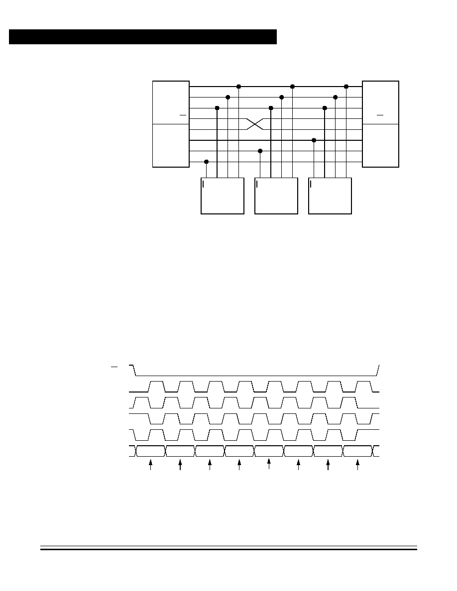
Technical Data
MC68HC705C8A -- Rev. 3
146
Serial Peripheral Interface (SPI)
MOTOROLA
Serial Peripheral Interface (SPI)
Figure 11-5. Two Master/Slaves and Three Slaves Block Diagram
11.6 Serial Clock Polarity and Phase
To accommodate the different serial communication requirements of
peripheral devices, software can change the phase and polarity of the
SPI serial clock. The clock polarity bit (CPOL) and the clock phase bit
(CPHA), both in the SPCR, control the timing relationship between the
serial clock and the transmitted data.
Figure 11-6
shows how the CPOL
and CPHA bits affect the clock/data timing.
Figure 11-6. SPI Clock/Data Timing
SLAVE MCU 2
SLAVE MCU 1
SLAVE MCU 0
PD
5/
S
S
PD
4/
SC
K
PD
3/
M
O
SI
PD
2/
M
I
S
O
MASTER/SLAVE
PD
5/
S
S
PD
4/
SC
K
PD
3/
M
O
SI
PD
2/
M
I
S
O
PD
5/
S
S
PD
4/
SC
K
PD
3/
M
O
SI
PD
2/
M
I
S
O
PD2/MISO
PD3/MOSI
PD4/SCK
PD5/SS
I/O
0
1
2
PORT
3
PD2/MISO
PD3/MOSI
PD4/SCK
PD5/SS
I/O
0
1
2
PORT
3
MCU 1
MASTER/SLAVE
MCU 2
MSB
BIT 6
BIT 5
BIT 4
BIT 3
BIT 2
BIT 1
LSB
SDO/SDI
1
0
1
0
SS
1
1
0
0
SCK (D)
SCK (C)
SCK (B)
SCK (A)
CPHA
CPOL
CAPTURE STROBE

Serial Peripheral Interface (SPI)
SPI Error Conditions
MC68HC705C8A -- Rev. 3
Technical Data
MOTOROLA
Serial Peripheral Interface (SPI)
147
11.7 SPI Error Conditions
These conditions produce SPI system errors:
∑
Bus contention caused by multiple master SPIs (mode fault error)
∑
Writing to the SPDR during a transmission (write-collision error)
∑
Failing to read the SPDR before the next incoming byte sets the
SPIF bit (overrun error)
11.7.1 Mode Fault Error
A mode fault error results when a logic 0 occurs on the PD5/SS pin of a
master SPI. The MCU takes these actions when a mode fault error
occurs:
∑
Puts the SPI in slave mode by clearing the MSTR bit
∑
Disables the SPI by clearing the SPE bit
∑
Sets the MODF bit
11.7.2 Write Collision Error
Writing to the SPDR during a transmission causes a write collision error
and sets the WCOL bit in the SPSR. Either a master SPI or a slave SPI
can generate a write collision error.
∑
Master -- A master SPI can cause a write collision error by writing
to the SPDR while the previously written byte is still being shifted
out to the PD3/MOSI pin. The error does not affect the
transmission of the previously written byte, but the byte that
caused the error is lost.
∑
Slave -- A slave SPI can cause a write collision error in either of
two ways, depending on the state of the CPHA bit:
≠
CPHA = 0 -- A slave SPI can cause a write collision error by
writing to the SPDR while the PD5/SS pin is at logic 0. The
error does not affect the byte in the SPDR, but the byte that
caused the error is lost.

Technical Data
MC68HC705C8A -- Rev. 3
148
Serial Peripheral Interface (SPI)
MOTOROLA
Serial Peripheral Interface (SPI)
≠
CPHA = 1 -- A slave SPI can cause a write collision error by
writing to the SPDR while receiving a transmission, that is,
between the first active SCK edge and the end of the eighth
SCK cycle. The error does not affect the transmission from the
master SPI, but the byte that caused the error is lost.
11.7.3 Overrun Error
Failing to read the byte in the SPDR before a subsequent byte enters the
shift register causes an overrun condition. In an overrun condition, all
incoming data is lost until software clears SPIF. The overrun condition
has no flag.
11.8 SPI Interrupts
The SPIF bit in the SPSR indicates a byte has shifted into or out of the
SPDR. The SPIF bit is a source of SPI interrupt requests. The SPI
interrupt enable bit (SPIE) in the SPCR is the local mask for SPIF
interrupts.
The MODF bit in the SPSR indicates a mode error and is a source of SPI
interrupt requests. The MODF bit is set when a logic 0 occurs on the
PD5/SS pin while the MSTR bit is set. The SPI interrupt enable bit (SPIE)
in the SPCR is the local mask for MODF interrupts.
11.9 SPI I/O Registers
These input/output (I/O) registers control and monitor SPI operation:
∑
SPI data register (SPDR)
∑
SPI control register (SPCR)
∑
SPI status register (SPSR)
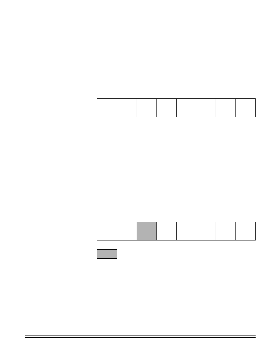
Serial Peripheral Interface (SPI)
SPI I/O Registers
MC68HC705C8A -- Rev. 3
Technical Data
MOTOROLA
Serial Peripheral Interface (SPI)
149
11.9.1 SPI Data Register
The SPDR shown in
Figure 11-7
is the read buffer for characters
received by the SPI. Writing a byte to the SPDR places the byte directly
into the SPI shift register.
11.9.2 SPI Control Register
∑
Enables SPI interrupt requests
∑
Enables the SPI
∑
Configures the SPI as master or slave
∑
Selects serial clock polarity, phase, and frequency
SPIE -- SPI Interrupt Enable Bit
This read/write bit enables SPI interrupts. Reset clears the SPIE bit.
1 = SPI interrupts enabled
0 = SPI interrupts disabled
Address:
$000C
Bit 7
6
5
4
3
2
1
Bit 0
Read:
Bit 7
Bit 6
Bit 5
Bit 4
Bit 3
Bit 2
Bit 1
Bit 0
Write:
Reset:
Unaffected by reset
Figure 11-7. SPI Data Register (SPDR)
Address:
$000A
Bit 7
6
5
4
3
2
1
Bit 0
Read:
SPIE
SPE
MSTR
CPOL
CPHA
SPR1
SPR0
Write:
Reset:
0
0
0
U
U
U
U
= Unimplemented
U = Unaffected
Figure 11-8. SPI Control Register (SPCR)

Technical Data
MC68HC705C8A -- Rev. 3
150
Serial Peripheral Interface (SPI)
MOTOROLA
Serial Peripheral Interface (SPI)
SPI -- SPI Enable Bit
This read/write bit enables the SPI. Reset clears the SPE bit.
1 = SPI enabled
0 = SPI disabled
MSTR -- Master Bit
This read/write bit selects master mode operation or slave mode
operation. Reset clears the MSTR bit.
1 = Master mode
0 = Slave mode
CPOL -- Clock Polarity Bit
This read/write bit determines the logic state of the PD4/SCK pin
between transmissions. To transmit data between SPIs, the SPIs
must have identical CPOL bits. Reset has no effect on the CPOL bit.
1 = PD4/SCK pin at logic 1 between transmissions
0 = PD4/SCK pin at logic 0 between transmissions
CPHA -- Clock Phase Bit
This read/write bit controls the timing relationship between the serial
clock and SPI data. To transmit data between SPIs, the SPIs must
have identical CPHA bits. When CPHA = 0, the PD5/SS pin of the
slave SPI must be set to logic 1 between bytes. Reset has no effect
on the CPHA bit.
1 = Edge following first active edge on PD4/SCK latches data
0 = First active edge on PD4/SCK latches data
SPR1 and SPR0 -- SPI Clock Rate Bits
These read/write bits select the master mode serial clock rate, as
shown in
Table 11-1
. The SPR1 and SPR0 bits of a slave SPI have
no effect on the serial clock. Reset has no effect on SPR1 and SPR0.
Table 11-1. SPI Clock Rate Selection
SPR[1:0]
SPI Clock Rate
00
Internal Clock
˜
2
01
Internal Clock
˜
4
10
Internal Clock
˜
16
11
Internal Clock
˜
32

Serial Peripheral Interface (SPI)
SPI I/O Registers
MC68HC705C8A -- Rev. 3
Technical Data
MOTOROLA
Serial Peripheral Interface (SPI)
151
11.9.3 SPI Status Register
The SPSR shown in
Figure 11-9
contains flags to signal these
conditions:
∑
SPI transmission complete
∑
Write collision
∑
Mode fault
SPIF -- SPI Flag
This clearable, read-only bit is set each time a byte shifts out of or into
the shift register. SPIF generates an interrupt request if the SPIE bit
in the SPCR is also set. Clear SPIF by reading the SPSR with SPIF
set and then reading or writing the SPDR. Reset clears the SPIF bit.
1 = Transmission complete
0 = Transmission not complete
WCOL -- Write Collision Bit
This clearable, read-only flag is set when software writes to the SPDR
while a transmission is in progress. Clear the WCOL bit by reading the
SPSR with WCOL set and then reading or writing the SPDR. Reset
clears WCOL.
1 = Invalid write to SPDR
0 = No invalid write to SPDR
Address:
$000B
Bit 7
6
5
4
3
2
1
Bit 0
Read:
SPIF
WCOL
MODF
Write:
Reset:
0
0
0
= Unimplemented
Figure 11-9. SPI Status Register (SPSR)

Technical Data
MC68HC705C8A -- Rev. 3
152
Serial Peripheral Interface (SPI)
MOTOROLA
Serial Peripheral Interface (SPI)
MODF -- Mode Fault Bit
This clearable, read-only bit is set when a logic 0 occurs on the
PD5/SS pin while the MSTR bit is set. MODF generates an interrupt
request if the SPIE bit is also set. Clear the MODF bit by reading the
SPSR with MODF set and then writing to the SPCR. Reset clears
MODF.
1 = PD5/SS pulled low while MSTR bit set
0 = PD5/SS not pulled low while MSTR bit set

MC68HC705C8A -- Rev. 3
Technical Data
MOTOROLA
Instruction Set
153
Technical Data -- MC68HC705C8A
Section 12. Instruction Set
12.1 Contents
12.2
Introduction . . . . . . . . . . . . . . . . . . . . . . . . . . . . . . . . . . . . . . . 154
12.3
Addressing Modes . . . . . . . . . . . . . . . . . . . . . . . . . . . . . . . . . 154
12.3.1
Inherent . . . . . . . . . . . . . . . . . . . . . . . . . . . . . . . . . . . . . . . 155
12.3.2
Immediate. . . . . . . . . . . . . . . . . . . . . . . . . . . . . . . . . . . . . . 155
12.3.3
Direct . . . . . . . . . . . . . . . . . . . . . . . . . . . . . . . . . . . . . . . . . 155
12.3.4
Extended . . . . . . . . . . . . . . . . . . . . . . . . . . . . . . . . . . . . . . 155
12.3.5
Indexed, No Offset . . . . . . . . . . . . . . . . . . . . . . . . . . . . . . . 156
12.3.6
Indexed, 8-Bit Offset. . . . . . . . . . . . . . . . . . . . . . . . . . . . . . 156
12.3.7
Indexed, 16-Bit Offset. . . . . . . . . . . . . . . . . . . . . . . . . . . . . 156
12.3.8
Relative . . . . . . . . . . . . . . . . . . . . . . . . . . . . . . . . . . . . . . . 157
12.4
Instruction Types . . . . . . . . . . . . . . . . . . . . . . . . . . . . . . . . . . 157
12.4.1
Register/Memory Instructions. . . . . . . . . . . . . . . . . . . . . . .158
12.4.2
Read-Modify-Write Instructions . . . . . . . . . . . . . . . . . . . . . 159
12.4.3
Jump/Branch Instructions. . . . . . . . . . . . . . . . . . . . . . . . . . 160
12.4.4
Bit Manipulation Instructions . . . . . . . . . . . . . . . . . . . . . . .162
12.4.5
Control Instructions . . . . . . . . . . . . . . . . . . . . . . . . . . . . . . 163
12.5
Instruction Set Summary . . . . . . . . . . . . . . . . . . . . . . . . . . . . 164
12.6
Opcode Map . . . . . . . . . . . . . . . . . . . . . . . . . . . . . . . . . . . . . . 169

Technical Data
MC68HC705C8A -- Rev. 3
154
Instruction Set
MOTOROLA
Instruction Set
12.2 Introduction
The MCU instruction set has 62 instructions and uses eight addressing
modes. The instructions include all those of the M146805 CMOS Family
plus one more: the unsigned multiply (MUL) instruction. The MUL
instruction allows unsigned multiplication of the contents of the
accumulator (A) and the index register (X). The high-order product is
stored in the index register, and the low-order product is stored in the
accumulator.
12.3 Addressing Modes
The CPU uses eight addressing modes for flexibility in accessing data.
The addressing modes provide eight different ways for the CPU to find
the data required to execute an instruction.
The eight addressing modes are:
∑
Inherent
∑
Immediate
∑
Direct
∑
Extended
∑
Indexed, no offset
∑
Indexed, 8-bit offset
∑
Indexed, 16-bit offset
∑
Relative

Instruction Set
Addressing Modes
MC68HC705C8A -- Rev. 3
Technical Data
MOTOROLA
Instruction Set
155
12.3.1 Inherent
Inherent instructions are those that have no operand, such as return
from interrupt (RTI) and stop (STOP). Some of the inherent instructions
act on data in the CPU registers, such as set carry flag (SEC) and
increment accumulator (INCA). Inherent instructions require no operand
address and are one byte long.
12.3.2 Immediate
Immediate instructions are those that contain a value to be used in an
operation with the value in the accumulator or index register. Immediate
instructions require no operand address and are two bytes long. The
opcode is the first byte, and the immediate data value is the second byte.
12.3.3 Direct
Direct instructions can access any of the first 256 memory locations with
two bytes. The first byte is the opcode, and the second is the low byte of
the operand address. In direct addressing, the CPU automatically uses
$00 as the high byte of the operand address.
12.3.4 Extended
Extended instructions use three bytes and can access any address in
memory. The first byte is the opcode; the second and third bytes are the
high and low bytes of the operand address.
When using the Motorola assembler, the programmer does not need to
specify whether an instruction is direct or extended. The assembler
automatically selects the shortest form of the instruction.

Technical Data
MC68HC705C8A -- Rev. 3
156
Instruction Set
MOTOROLA
Instruction Set
12.3.5 Indexed, No Offset
Indexed instructions with no offset are 1-byte instructions that can
access data with variable addresses within the first 256 memory
locations. The index register contains the low byte of the effective
address of the operand. The CPU automatically uses $00 as the high
byte, so these instructions can address locations $0000≠$00FF.
Indexed, no offset instructions are often used to move a pointer through
a table or to hold the address of a frequently used RAM or I/O location.
12.3.6 Indexed, 8-Bit Offset
Indexed, 8-bit offset instructions are 2-byte instructions that can access
data with variable addresses within the first 511 memory locations. The
CPU adds the unsigned byte in the index register to the unsigned byte
following the opcode. The sum is the effective address of the operand.
These instructions can access locations $0000≠$01FE.
Indexed 8-bit offset instructions are useful for selecting the kth element
in an n-element table. The table can begin anywhere within the first 256
memory locations and could extend as far as location 510 ($01FE). The
k value is typically in the index register, and the address of the beginning
of the table is in the byte following the opcode.
12.3.7 Indexed, 16-Bit Offset
Indexed, 16-bit offset instructions are 3-byte instructions that can access
data with variable addresses at any location in memory. The CPU adds
the unsigned byte in the index register to the two unsigned bytes
following the opcode. The sum is the effective address of the operand.
The first byte after the opcode is the high byte of the 16-bit offset; the
second byte is the low byte of the offset.
Indexed, 16-bit offset instructions are useful for selecting the kth element
in an n-element table anywhere in memory.
As with direct and extended addressing, the Motorola assembler
determines the shortest form of indexed addressing.

Instruction Set
Instruction Types
MC68HC705C8A -- Rev. 3
Technical Data
MOTOROLA
Instruction Set
157
12.3.8 Relative
Relative addressing is only for branch instructions. If the branch
condition is true, the CPU finds the effective branch destination by
adding the signed byte following the opcode to the contents of the
program counter. If the branch condition is not true, the CPU goes to the
next instruction. The offset is a signed, two's complement byte that gives
a branching range of ≠128 to +127 bytes from the address of the next
location after the branch instruction.
When using the Motorola assembler, the programmer does not need to
calculate the offset, because the assembler determines the proper offset
and verifies that it is within the span of the branch.
12.4 Instruction Types
The MCU instructions fall into five categories:
∑
Register/memory instructions
∑
Read-modify-write instructions
∑
Jump/branch instructions
∑
Bit manipulation instructions
∑
Control instructions

Technical Data
MC68HC705C8A -- Rev. 3
158
Instruction Set
MOTOROLA
Instruction Set
12.4.1 Register/Memory Instructions
These instructions operate on CPU registers and memory locations.
Most of them use two operands. One operand is in either the
accumulator or the index register. The CPU finds the other operand in
memory.
Table 12-1. Register/Memory Instructions
Instruction
Mnemonic
Add memory byte and carry bit to accumulator
ADC
Add memory byte to accumulator
ADD
AND memory byte with accumulator
AND
Bit test accumulator
BIT
Compare accumulator
CMP
Compare index register with memory byte
CPX
Exclusive OR accumulator with memory byte
EOR
Load accumulator with memory byte
LDA
Load Index register with memory byte
LDX
Multiply
MUL
OR accumulator with memory byte
ORA
Subtract memory byte and carry bit from
accumulator
SBC
Store accumulator in memory
STA
Store index register in memory
STX
Subtract memory byte from accumulator
SUB

Instruction Set
Instruction Types
MC68HC705C8A -- Rev. 3
Technical Data
MOTOROLA
Instruction Set
159
12.4.2 Read-Modify-Write Instructions
These instructions read a memory location or a register, modify its
contents, and write the modified value back to the memory location or to
the register.
NOTE:
Do not use read-modify-write operations on write-only registers.
Table 12-2. Read-Modify-Write Instructions
Instruction
Mnemonic
Arithmetic shift left (same as LSL)
ASL
Arithmetic shift right
ASR
Bit clear
BCLR
(1)
1. Unlike other read-modify-write instructions, BCLR and BSET use
only direct addressing.
Bit set
BSET
(1)
Clear register
CLR
Complement (one's complement)
COM
Decrement
DEC
Increment
INC
Logical shift left (same as ASL)
LSL
Logical shift right
LSR
Negate (two's complement)
NEG
Rotate left through carry bit
ROL
Rotate right through carry bit
ROR
Test for negative or zero
TST
(2)
2. TST is an exception to the read-modify-write sequence because it
does not write a replacement value.

Technical Data
MC68HC705C8A -- Rev. 3
160
Instruction Set
MOTOROLA
Instruction Set
12.4.3 Jump/Branch Instructions
Jump instructions allow the CPU to interrupt the normal sequence of the
program counter. The unconditional jump instruction (JMP) and the
jump-to-subroutine instruction (JSR) have no register operand. Branch
instructions allow the CPU to interrupt the normal sequence of the
program counter when a test condition is met. If the test condition is not
met, the branch is not performed.
The BRCLR and BRSET instructions cause a branch based on the state
of any readable bit in the first 256 memory locations. These 3-byte
instructions use a combination of direct addressing and relative
addressing. The direct address of the byte to be tested is in the byte
following the opcode. The third byte is the signed offset byte. The CPU
finds the effective branch destination by adding the third byte to the
program counter if the specified bit tests true. The bit to be tested and its
condition (set or clear) is part of the opcode. The span of branching is
from ≠128 to +127 from the address of the next location after the branch
instruction. The CPU also transfers the tested bit to the carry/borrow bit
of the condition code register.

Instruction Set
Instruction Types
MC68HC705C8A -- Rev. 3
Technical Data
MOTOROLA
Instruction Set
161
Table 12-3. Jump and Branch Instructions
Instruction
Mnemonic
Branch if carry bit clear
BCC
Branch if carry bit set
BCS
Branch if equal
BEQ
Branch if half-carry bit clear
BHCC
Branch if half-carry bit set
BHCS
Branch if higher
BHI
Branch if higher or same
BHS
Branch if IRQ pin high
BIH
Branch if IRQ pin low
BIL
Branch if lower
BLO
Branch if lower or same
BLS
Branch if interrupt mask clear
BMC
Branch if minus
BMI
Branch if interrupt mask set
BMS
Branch if not equal
BNE
Branch if plus
BPL
Branch always
BRA
Branch if bit clear
BRCLR
Branch never
BRN
Branch if bit set
BRSET
Branch to subroutine
BSR
Unconditional jump
JMP
Jump to subroutine
JSR

Technical Data
MC68HC705C8A -- Rev. 3
162
Instruction Set
MOTOROLA
Instruction Set
12.4.4 Bit Manipulation Instructions
The CPU can set or clear any writable bit in the first 256 bytes of
memory, which includes I/O registers and on-chip RAM locations. The
CPU can also test and branch based on the state of any bit in any of the
first 256 memory locations.
Table 12-4. Bit Manipulation Instructions
Instruction
Mnemonic
Bit clear
BCLR
Branch if bit clear
BRCLR
Branch if bit set
BRSET
Bit set
BSET

Instruction Set
Instruction Types
MC68HC705C8A -- Rev. 3
Technical Data
MOTOROLA
Instruction Set
163
12.4.5 Control Instructions
These instructions act on CPU registers and control CPU operation
during program execution.
Table 12-5. Control Instructions
Instruction
Mnemonic
Clear carry bit
CLC
Clear interrupt mask
CLI
No operation
NOP
Reset stack pointer
RSP
Return from interrupt
RTI
Return from subroutine
RTS
Set carry bit
SEC
Set interrupt mask
SEI
Stop oscillator and enable IRQ pin
STOP
Software interrupt
SWI
Transfer accumulator to index register
TAX
Transfer index register to accumulator
TXA
Stop CPU clock and enable interrupts
WAIT
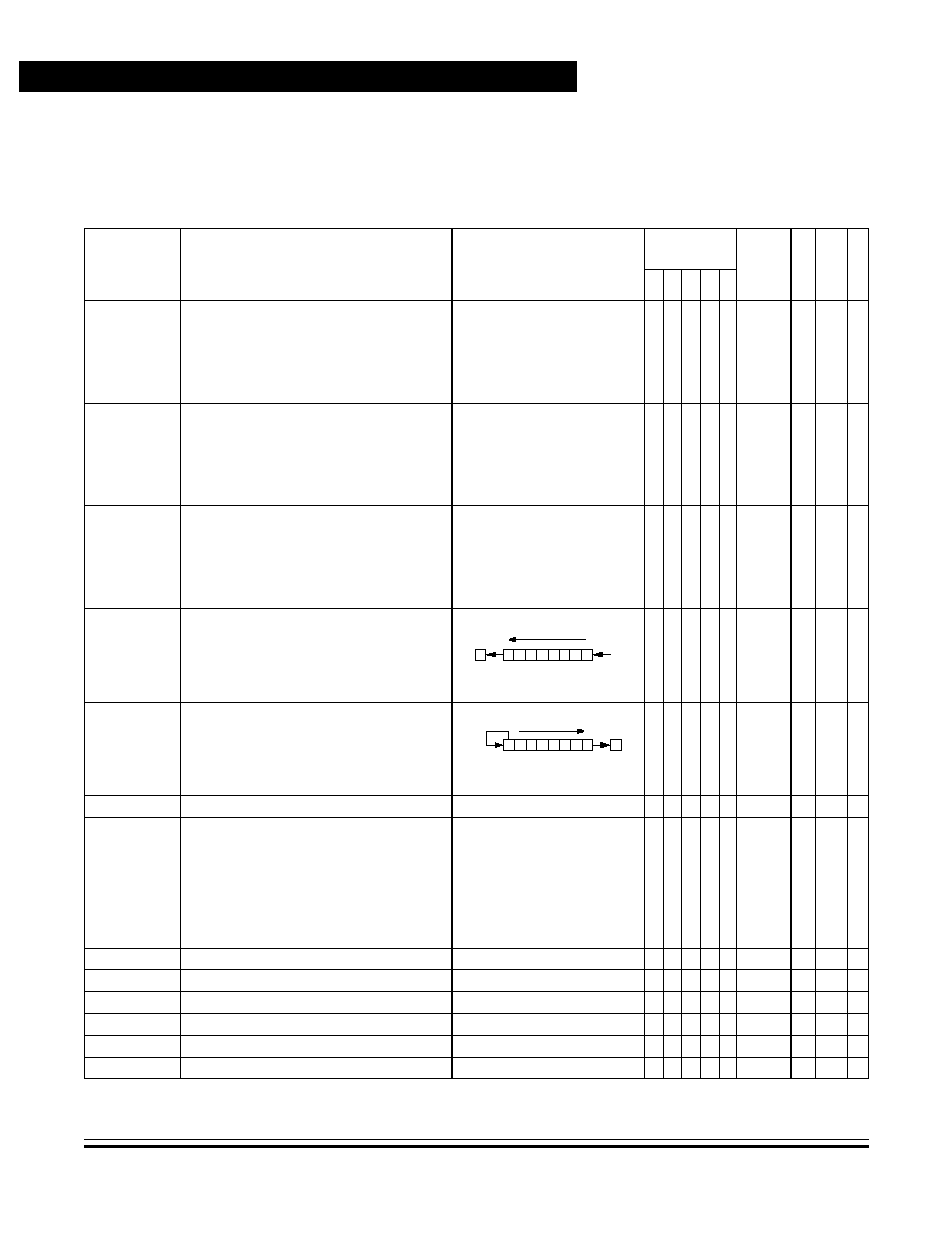
Technical Data
MC68HC705C8A -- Rev. 3
164
Instruction Set
MOTOROLA
Instruction Set
12.5 Instruction Set Summary
Table 12-6. Instruction Set Summary (Sheet 1 of 6)
Source
Form
Operation
Description
Effect on
CCR
Ad
d
r
ess
Mo
de
Op
c
o
d
e
Op
eran
d
Cycl
es
H I N Z C
ADC #opr
ADC opr
ADC opr
ADC opr,X
ADC opr,X
ADC ,X
Add with Carry
A
(A) + (M) + (C)
--
IMM
DIR
EXT
IX2
IX1
IX
A9
B9
C9
D9
E9
F9
ii
dd
hh ll
ee ff
ff
2
3
4
5
4
3
ADD #opr
ADD opr
ADD opr
ADD opr,X
ADD opr,X
ADD ,X
Add without Carry
A
(A) + (M)
--
IMM
DIR
EXT
IX2
IX1
IX
AB
BB
CB
DB
EB
FB
ii
dd
hh ll
ee ff
ff
2
3
4
5
4
3
AND #opr
AND opr
AND opr
AND opr,X
AND opr,X
AND ,X
Logical AND
A
(A)
(M)
-- --
--
IMM
DIR
EXT
IX2
IX1
IX
A4
B4
C4
D4
E4
F4
ii
dd
hh ll
ee ff
ff
2
3
4
5
4
3
ASL opr
ASLA
ASLX
ASL opr,X
ASL ,X
Arithmetic Shift Left (Same as LSL)
-- --
DIR
INH
INH
IX1
IX
38
48
58
68
78
dd
ff
5
3
3
6
5
ASR opr
ASRA
ASRX
ASR opr,X
ASR ,X
Arithmetic Shift Right
-- --
DIR
INH
INH
IX1
IX
37
47
57
67
77
dd
ff
5
3
3
6
5
BCC rel
Branch if Carry Bit Clear
PC
(PC) + 2 + rel ? C = 0
-- -- -- -- --
REL
24
rr
3
BCLR n opr
Clear Bit n
Mn
0
-- -- -- -- --
DIR (b0)
DIR (b1)
DIR (b2)
DIR (b3)
DIR (b4)
DIR (b5)
DIR (b6)
DIR (b7)
11
13
15
17
19
1B
1D
1F
dd
dd
dd
dd
dd
dd
dd
dd
5
5
5
5
5
5
5
5
BCS rel
Branch if Carry Bit Set (Same as BLO)
PC
(PC) + 2 + rel ? C = 1
-- -- -- -- --
REL
25
rr
3
BEQ rel
Branch if Equal
PC
(PC) + 2 + rel ? Z = 1
-- -- -- -- --
REL
27
rr
3
BHCC rel
Branch if Half-Carry Bit Clear
PC
(PC) + 2 + rel ? H = 0
-- -- -- -- --
REL
28
rr
3
BHCS rel
Branch if Half-Carry Bit Set
PC
(PC) + 2 + rel ? H = 1
-- -- -- -- --
REL
29
rr
3
BHI rel
Branch if Higher
PC
(PC) + 2 + rel ? C
Z = 0 -- -- -- -- --
REL
22
rr
3
BHS rel
Branch if Higher or Same
PC
(PC) + 2 + rel ? C = 0
-- -- -- -- --
REL
24
rr
3
C
b0
b7
0
b0
b7
C

Instruction Set
Instruction Set Summary
MC68HC705C8A -- Rev. 3
Technical Data
MOTOROLA
Instruction Set
165
BIH rel
Branch if IRQ Pin High
PC
(PC) + 2 + rel ? IRQ = 1
-- -- -- -- --
REL
2F
rr
3
BIL rel
Branch if IRQ Pin Low
PC
(PC) + 2 + rel ? IRQ = 0
-- -- -- -- --
REL
2E
rr
3
BIT #opr
BIT opr
BIT opr
BIT opr,X
BIT opr,X
BIT ,X
Bit Test Accumulator with Memory Byte
(A)
(M)
-- --
--
IMM
DIR
EXT
IX2
IX1
IX
A5
B5
C5
D5
E5
F5
ii
dd
hh ll
ee ff
ff
2
3
4
5
4
3
BLO rel
Branch if Lower (Same as BCS)
PC
(PC) + 2 + rel ? C = 1
-- -- -- -- --
REL
25
rr
3
BLS rel
Branch if Lower or Same
PC
(PC) + 2 + rel ? C
Z = 1 -- -- -- -- --
REL
23
rr
3
BMC rel
Branch if Interrupt Mask Clear
PC
(PC) + 2 + rel ? I = 0
-- -- -- -- --
REL
2C
rr
3
BMI rel
Branch if Minus
PC
(PC) + 2 + rel ? N = 1
-- -- -- -- --
REL
2B
rr
3
BMS rel
Branch if Interrupt Mask Set
PC
(PC) + 2 + rel ? I = 1
-- -- -- -- --
REL
2D
rr
3
BNE rel
Branch if Not Equal
PC
(PC) + 2 + rel ? Z = 0
-- -- -- -- --
REL
26
rr
3
BPL rel
Branch if Plus
PC
(PC) + 2 + rel ? N = 0
-- -- -- -- --
REL
2A
rr
3
BRA rel
Branch Always
PC
(PC) + 2 + rel ? 1 = 1
-- -- -- -- --
REL
20
rr
3
BRCLR n opr rel Branch if Bit n Clear
PC
(PC) + 2 + rel ? Mn = 0
-- -- -- --
DIR (b0)
DIR (b1)
DIR (b2)
DIR (b3)
DIR (b4)
DIR (b5)
DIR (b6)
DIR (b7)
01
03
05
07
09
0B
0D
0F
dd rr
dd rr
dd rr
dd rr
dd rr
dd rr
dd rr
dd rr
5
5
5
5
5
5
5
5
BRN rel
Branch Never
PC
(PC) + 2 + rel ? 1 = 0
-- -- -- -- --
REL
21
rr
3
BRSET n opr rel Branch if Bit n Set
PC
(PC) + 2 + rel ? Mn = 1
-- -- -- --
DIR (b0)
DIR (b1)
DIR (b2)
DIR (b3)
DIR (b4)
DIR (b5)
DIR (b6)
DIR (b7)
00
02
04
06
08
0A
0C
0E
dd rr
dd rr
dd rr
dd rr
dd rr
dd rr
dd rr
dd rr
5
5
5
5
5
5
5
5
BSET n opr
Set Bit n
Mn
1
-- -- -- -- --
DIR (b0)
DIR (b1)
DIR (b2)
DIR (b3)
DIR (b4)
DIR (b5)
DIR (b6)
DIR (b7)
10
12
14
16
18
1A
1C
1E
dd
dd
dd
dd
dd
dd
dd
dd
5
5
5
5
5
5
5
5
BSR rel
Branch to Subroutine
PC
(PC) + 2; push (PCL)
SP
(SP) ≠ 1; push (PCH)
SP
(SP) ≠ 1
PC
(PC) + rel
-- -- -- -- --
REL
AD
rr
6
CLC
Clear Carry Bit
C
0
-- -- -- -- 0
INH
98
2
CLI
Clear Interrupt Mask
I
0
-- 0 -- -- --
INH
9A
2
Table 12-6. Instruction Set Summary (Sheet 2 of 6)
Source
Form
Operation
Description
Effect on
CCR
Ad
d
r
ess
M
ode
Op
cod
e
Ope
r
and
Cycl
es
H I N Z C

Technical Data
MC68HC705C8A -- Rev. 3
166
Instruction Set
MOTOROLA
Instruction Set
CLR opr
CLRA
CLRX
CLR opr,X
CLR ,X
Clear Byte
M
$00
A
$00
X
$00
M
$00
M
$00
-- -- 0
1 --
DIR
INH
INH
IX1
IX
3F
4F
5F
6F
7F
dd
ff
5
3
3
6
5
CMP #opr
CMP opr
CMP opr
CMP opr,X
CMP opr,X
CMP ,X
Compare Accumulator with Memory Byte
(A) ≠ (M)
-- --
IMM
DIR
EXT
IX2
IX1
IX
A1
B1
C1
D1
E1
F1
ii
dd
hh ll
ee ff
ff
2
3
4
5
4
3
COM opr
COMA
COMX
COM opr,X
COM ,X
Complement Byte (One's Complement)
M
(M) = $FF ≠ (M)
A
(A) = $FF ≠ (A)
X
(X) = $FF ≠ (X)
M
(M) = $FF ≠ (M)
M
(M) = $FF ≠ (M)
-- --
1
DIR
INH
INH
IX1
IX
33
43
53
63
73
dd
ff
5
3
3
6
5
CPX #opr
CPX opr
CPX opr
CPX opr,X
CPX opr,X
CPX ,X
Compare Index Register with Memory Byte
(X) ≠ (M)
-- --
IMM
DIR
EXT
IX2
IX1
IX
A3
B3
C3
D3
E3
F3
ii
dd
hh ll
ee ff
ff
2
3
4
5
4
3
DEC opr
DECA
DECX
DEC opr,X
DEC ,X
Decrement Byte
M
(M) ≠ 1
A
(A) ≠ 1
X
(X) ≠ 1
M
(M) ≠ 1
M
(M) ≠ 1
-- --
--
DIR
INH
INH
IX1
IX
3A
4A
5A
6A
7A
dd
ff
5
3
3
6
5
EOR #opr
EOR opr
EOR opr
EOR opr,X
EOR opr,X
EOR ,X
EXCLUSIVE OR Accumulator with Memory
Byte
A
(A)
(M)
-- --
--
IMM
DIR
EXT
IX2
IX1
IX
A8
B8
C8
D8
E8
F8
ii
dd
hh ll
ee ff
ff
2
3
4
5
4
3
INC opr
INCA
INCX
INC opr,X
INC ,X
Increment Byte
M
(M) + 1
A
(A) + 1
X
(X) + 1
M
(M) + 1
M
(M) + 1
-- --
--
DIR
INH
INH
IX1
IX
3C
4C
5C
6C
7C
dd
ff
5
3
3
6
5
JMP opr
JMP opr
JMP opr,X
JMP opr,X
JMP ,X
Unconditional Jump
PC
Jump Address
-- -- -- -- --
DIR
EXT
IX2
IX1
IX
BC
CC
DC
EC
FC
dd
hh ll
ee ff
ff
2
3
4
3
2
Table 12-6. Instruction Set Summary (Sheet 3 of 6)
Source
Form
Operation
Description
Effect on
CCR
Ad
d
r
ess
M
ode
Op
cod
e
Ope
r
and
Cycl
es
H I N Z C

Instruction Set
Instruction Set Summary
MC68HC705C8A -- Rev. 3
Technical Data
MOTOROLA
Instruction Set
167
JSR opr
JSR opr
JSR opr,X
JSR opr,X
JSR ,X
Jump to Subroutine
PC
(PC) + n (n = 1, 2, or 3)
Push (PCL); SP
(SP) ≠ 1
Push (PCH); SP
(SP) ≠ 1
PC
Effective Address
-- -- -- -- --
DIR
EXT
IX2
IX1
IX
BD
CD
DD
ED
FD
dd
hh ll
ee ff
ff
5
6
7
6
5
LDA #opr
LDA opr
LDA opr
LDA opr,X
LDA opr,X
LDA ,X
Load Accumulator with Memory Byte
A
(M)
-- --
--
IMM
DIR
EXT
IX2
IX1
IX
A6
B6
C6
D6
E6
F6
ii
dd
hh ll
ee ff
ff
2
3
4
5
4
3
LDX #opr
LDX opr
LDX opr
LDX opr,X
LDX opr,X
LDX ,X
Load Index Register with Memory Byte
X
(M)
-- --
--
IMM
DIR
EXT
IX2
IX1
IX
AE
BE
CE
DE
EE
FE
ii
dd
hh ll
ee ff
ff
2
3
4
5
4
3
LSL opr
LSLA
LSLX
LSL opr,X
LSL ,X
Logical Shift Left (Same as ASL)
-- --
DIR
INH
INH
IX1
IX
38
48
58
68
78
dd
ff
5
3
3
6
5
LSR opr
LSRA
LSRX
LSR opr,X
LSR ,X
Logical Shift Right
-- -- 0
DIR
INH
INH
IX1
IX
34
44
54
64
74
dd
ff
5
3
3
6
5
MUL
Unsigned Multiply
X : A
(X)
◊
(A)
0 -- -- -- 0
INH
42
1
1
NEG opr
NEGA
NEGX
NEG opr,X
NEG ,X
Negate Byte (Two's Complement)
M
≠(M) = $00 ≠ (M)
A
≠(A) = $00 ≠ (A)
X
≠(X) = $00 ≠ (X)
M
≠(M) = $00 ≠ (M)
M
≠(M) = $00 ≠ (M)
-- --
DIR
INH
INH
IX1
IX
30
40
50
60
70
dd
ff
5
3
3
6
5
NOP
No Operation
-- -- -- -- --
INH
9D
2
ORA #opr
ORA opr
ORA opr
ORA opr,X
ORA opr,X
ORA ,X
Logical OR Accumulator with Memory
A
(A)
(M)
-- --
--
IMM
DIR
EXT
IX2
IX1
IX
AA
BA
CA
DA
EA
FA
ii
dd
hh ll
ee ff
ff
2
3
4
5
4
3
ROL opr
ROLA
ROLX
ROL opr,X
ROL ,X
Rotate Byte Left through Carry Bit
-- --
DIR
INH
INH
IX1
IX
39
49
59
69
79
dd
ff
5
3
3
6
5
Table 12-6. Instruction Set Summary (Sheet 4 of 6)
Source
Form
Operation
Description
Effect on
CCR
Ad
d
r
ess
M
ode
Op
cod
e
Ope
r
and
Cycl
es
H I N Z C
C
b0
b7
0
b0
b7
C
0
C
b0
b7
Technical Data
MC68HC705C8A -- Rev. 3
168
Instruction Set
MOTOROLA
Instruction Set
ROR opr
RORA
RORX
ROR opr,X
ROR ,X
Rotate Byte Right through Carry Bit
-- --
DIR
INH
INH
IX1
IX
36
46
56
66
76
dd
ff
5
3
3
6
5
RSP
Reset Stack Pointer
SP
$00FF
-- -- -- -- --
INH
9C
2
RTI
Return from Interrupt
SP
(SP) + 1; Pull (CCR)
SP
(SP) + 1; Pull (A)
SP
(SP) + 1; Pull (X)
SP
(SP) + 1; Pull (PCH)
SP
(SP) + 1; Pull (PCL)
INH
80
9
RTS
Return from Subroutine
SP
(SP) + 1; Pull (PCH)
SP
(SP) + 1; Pull (PCL)
-- -- -- -- --
INH
81
6
SBC #opr
SBC opr
SBC opr
SBC opr,X
SBC opr,X
SBC ,X
Subtract Memory Byte and Carry Bit from
Accumulator
A
(A) ≠ (M) ≠ (C)
-- --
IMM
DIR
EXT
IX2
IX1
IX
A2
B2
C2
D2
E2
F2
ii
dd
hh ll
ee ff
ff
2
3
4
5
4
3
SEC
Set Carry Bit
C
1
-- -- -- -- 1
INH
99
2
SEI
Set Interrupt Mask
I
1
-- 1 -- -- --
INH
9B
2
STA opr
STA opr
STA opr,X
STA opr,X
STA ,X
Store Accumulator in Memory
M
(A)
-- --
--
DIR
EXT
IX2
IX1
IX
B7
C7
D7
E7
F7
dd
hh ll
ee ff
ff
4
5
6
5
4
STOP
Stop Oscillator and Enable IRQ Pin
-- 0 -- -- --
INH
8E
2
STX opr
STX opr
STX opr,X
STX opr,X
STX ,X
Store Index Register In Memory
M
(X)
-- --
--
DIR
EXT
IX2
IX1
IX
BF
CF
DF
EF
FF
dd
hh ll
ee ff
ff
4
5
6
5
4
SUB #opr
SUB opr
SUB opr
SUB opr,X
SUB opr,X
SUB ,X
Subtract Memory Byte from Accumulator
A
(A) ≠ (M)
-- --
IMM
DIR
EXT
IX2
IX1
IX
A0
B0
C0
D0
E0
F0
ii
dd
hh ll
ee ff
ff
2
3
4
5
4
3
SWI
Software Interrupt
PC
(PC) + 1; Push (PCL)
SP
(SP) ≠ 1; Push (PCH)
SP
(SP) ≠ 1; Push (X)
SP
(SP) ≠ 1; Push (A)
SP
(SP) ≠ 1; Push (CCR)
SP
(SP) ≠ 1; I
1
PCH
Interrupt Vector High Byte
PCL
Interrupt Vector Low Byte
-- 1 -- -- --
INH
83
1
0
TAX
Transfer Accumulator to Index Register
X
(A)
-- -- -- -- --
INH
97
2
Table 12-6. Instruction Set Summary (Sheet 5 of 6)
Source
Form
Operation
Description
Effect on
CCR
Ad
d
r
ess
M
ode
Op
cod
e
Ope
r
and
Cycl
es
H I N Z C
b0
b7
C

Instruction Set
Opcode Map
MC68HC705C8A -- Rev. 3
Technical Data
MOTOROLA
Instruction Set
169
12.6 Opcode Map
See
Table 12-7
.
TST opr
TSTA
TSTX
TST opr,X
TST ,X
Test Memory Byte for Negative or Zero
(M) ≠ $00
-- --
--
DIR
INH
INH
IX1
IX
3D
4D
5D
6D
7D
dd
ff
4
3
3
5
4
TXA
Transfer Index Register to Accumulator
A
(X)
-- -- -- -- --
INH
9F
2
WAIT
Stop CPU Clock and Enable Interrupts
--
-- -- --
INH
8F
2
A
Accumulator
opr
Operand (one or two bytes)
C
Carry/borrow flag
PC
Program counter
CCR
Condition code register
PCH
Program counter high byte
dd
Direct address of operand
PCL
Program counter low byte
dd rr
Direct address of operand and relative offset of branch instruction
REL
Relative addressing mode
DIR
Direct addressing mode
rel
Relative program counter offset byte
ee ff
High and low bytes of offset in indexed, 16-bit offset addressing
rr
Relative program counter offset byte
EXT
Extended addressing mode
SP
Stack pointer
ff
Offset byte in indexed, 8-bit offset addressing
X
Index register
H
Half-carry flag
Z
Zero flag
hh ll
High and low bytes of operand address in extended addressing
#
Immediate value
I
Interrupt mask
Logical AND
ii
Immediate operand byte
Logical OR
IMM
Immediate addressing mode
Logical EXCLUSIVE OR
INH
Inherent addressing mode
( )
Contents of
IX
Indexed, no offset addressing mode
≠( )
Negation (two's complement)
IX1
Indexed, 8-bit offset addressing mode
Loaded with
IX2
Indexed, 16-bit offset addressing mode
?
If
M
Memory location
:
Concatenated with
N
Negative flag
Set or cleared
n
Any bit
--
Not affected
Table 12-6. Instruction Set Summary (Sheet 6 of 6)
Source
Form
Operation
Description
Effect on
CCR
Ad
d
r
ess
M
ode
Op
cod
e
Ope
r
and
Cycl
es
H I N Z C
T
e
c
hni
c
a
l
Dat
a
M
C
68HC7
05C8A
--
Rev
.
3
170
I
n
s
t
ruc
t
i
on S
e
t
M
O
T
O
R
OLA
In
st
r
u
ct
io
n S
e
t
Table 12-7. Opcode Map
Bit Manipulation
Branch
Read-Modify-Write
Control
Register/Memory
DIR
DIR
REL
DIR
INH
INH
IX1
IX
INH
INH
IMM
DIR
EXT
IX2
IX1
IX
0
1
2
3
4
5
6
7
8
9
A
B
C
D
E
F
0
5
BRSET0
3
DIR
5
BSET0
2
DIR
3
BRA
2
REL
5
NEG
2
DIR
3
NEGA
1
INH
3
NEGX
1
INH
6
NEG
2
IX1
5
NEG
1
IX
9
RTI
1
INH
2
SUB
2
IMM
3
SUB
2
DIR
4
SUB
3
EXT
5
SUB
3
IX2
4
SUB
2
IX1
3
SUB
1
IX
0
1
5
BRCLR0
3
DIR
5
BCLR0
2
DIR
3
BRN
2
REL
6
RTS
1
INH
2
CMP
2
IMM
3
CMP
2
DIR
4
CMP
3
EXT
5
CMP
3
IX2
4
CMP
2
IX1
3
CMP
1
IX
1
2
5
BRSET1
3
DIR
5
BSET1
2
DIR
3
BHI
2
REL
11
MUL
1
INH
2
SBC
2
IMM
3
SBC
2
DIR
4
SBC
3
EXT
5
SBC
3
IX2
4
SBC
2
IX1
3
SBC
1
IX
2
3
5
BRCLR1
3
DIR
5
BCLR1
2
DIR
3
BLS
2
REL
5
COM
2
DIR
3
COMA
1
INH
3
COMX
1
INH
6
COM
2
IX1
5
COM
1
IX
10
SWI
1
INH
2
CPX
2
IMM
3
CPX
2
DIR
4
CPX
3
EXT
5
CPX
3
IX2
4
CPX
2
IX1
3
CPX
1
IX
3
4
5
BRSET2
3
DIR
5
BSET2
2
DIR
3
BCC
2
REL
5
LSR
2
DIR
3
LSRA
1
INH
3
LSRX
1
INH
6
LSR
2
IX1
5
LSR
1
IX
2
AND
2
IMM
3
AND
2
DIR
4
AND
3
EXT
5
AND
3
IX2
4
AND
2
IX1
3
AND
1
IX
4
5
5
BRCLR2
3
DIR
5
BCLR2
2
DIR
3
BCS/BLO
2
REL
2
BIT
2
IMM
3
BIT
2
DIR
4
BIT
3
EXT
5
BIT
3
IX2
4
BIT
2
IX1
3
BIT
1
IX
5
6
5
BRSET3
3
DIR
5
BSET3
2
DIR
3
BNE
2
REL
5
ROR
2
DIR
3
RORA
1
INH
3
RORX
1
INH
6
ROR
2
IX1
5
ROR
1
IX
2
LDA
2
IMM
3
LDA
2
DIR
4
LDA
3
EXT
5
LDA
3
IX2
4
LDA
2
IX1
3
LDA
1
IX
6
7
5
BRCLR3
3
DIR
5
BCLR3
2
DIR
3
BEQ
2
REL
5
ASR
2
DIR
3
ASRA
1
INH
3
ASRX
1
INH
6
ASR
2
IX1
5
ASR
1
IX
2
TAX
1
INH
4
STA
2
DIR
5
STA
3
EXT
6
STA
3
IX2
5
STA
2
IX1
4
STA
1
IX
7
8
5
BRSET4
3
DIR
5
BSET4
2
DIR
3
BHCC
2
REL
5
ASL/LSL
2
DIR
3
ASLA/LSLA
1
INH
3
ASLX/LSLX
1
INH
6
ASL/LSL
2
IX1
5
ASL/LSL
1
IX
2
CLC
1
INH
2
EOR
2
IMM
3
EOR
2
DIR
4
EOR
3
EXT
5
EOR
3
IX2
4
EOR
2
IX1
3
EOR
1
IX
8
9
5
BRCLR4
3
DIR
5
BCLR4
2
DIR
3
BHCS
2
REL
5
ROL
2
DIR
3
ROLA
1
INH
3
ROLX
1
INH
6
ROL
2
IX1
5
ROL
1
IX
2
SEC
1
INH
2
ADC
2
IMM
3
ADC
2
DIR
4
ADC
3
EXT
5
ADC
3
IX2
4
ADC
2
IX1
3
ADC
1
IX
9
A
5
BRSET5
3
DIR
5
BSET5
2
DIR
3
BPL
2
REL
5
DEC
2
DIR
3
DECA
1
INH
3
DECX
1
INH
6
DEC
2
IX1
5
DEC
1
IX
2
CLI
1
INH
2
ORA
2
IMM
3
ORA
2
DIR
4
ORA
3
EXT
5
ORA
3
IX2
4
ORA
2
IX1
3
ORA
1
IX
A
B
5
BRCLR5
3
DIR
5
BCLR5
2
DIR
3
BMI
2
REL
2
SEI
1
INH
2
ADD
2
IMM
3
ADD
2
DIR
4
ADD
3
EXT
5
ADD
3
IX2
4
ADD
2
IX1
3
ADD
1
IX
B
C
5
BRSET6
3
DIR
5
BSET6
2
DIR
3
BMC
2
REL
5
INC
2
DIR
3
INCA
1
INH
3
INCX
1
INH
6
INC
2
IX1
5
INC
1
IX
2
RSP
1
INH
2
JMP
2
DIR
3
JMP
3
EXT
4
JMP
3
IX2
3
JMP
2
IX1
2
JMP
1
IX
C
D
5
BRCLR6
3
DIR
5
BCLR6
2
DIR
3
BMS
2
REL
4
TST
2
DIR
3
TSTA
1
INH
3
TSTX
1
INH
5
TST
2
IX1
4
TST
1
IX
2
NOP
1
INH
6
BSR
2
REL
5
JSR
2
DIR
6
JSR
3
EXT
7
JSR
3
IX2
6
JSR
2
IX1
5
JSR
1
IX
D
E
5
BRSET7
3
DIR
5
BSET7
2
DIR
3
BIL
2
REL
2
STOP
1
INH
2
LDX
2
IMM
3
LDX
2
DIR
4
LDX
3
EXT
5
LDX
3
IX2
4
LDX
2
IX1
3
LDX
1
IX
E
F
5
BRCLR7
3
DIR
5
BCLR7
2
DIR
3
BIH
2
REL
5
CLR
2
DIR
3
CLRA
1
INH
3
CLRX
1
INH
6
CLR
2
IX1
5
CLR
1
IX
2
WAIT
1
INH
2
TXA
1
INH
4
STX
2
DIR
5
STX
3
EXT
6
STX
3
IX2
5
STX
2
IX1
4
STX
1
IX
F
INH = Inherent
REL = Relative
IMM = Immediate
IX = Indexed, No Offset
DIR = Direct
IX1 = Indexed, 8-Bit Offset
EXT = Extended
IX2 = Indexed, 16-Bit Offset
0
MSB of Opcode in Hexadecimal
LSB of Opcode in Hexadecimal
0
5
BRSET0
3
DIR
Number of Cycles
Opcode Mnemonic
Number of Bytes/Addressing Mode
LSB
MSB
LSB
MSB
LSB
MSB

MC68HC705C8A -- Rev. 3
Technical Data
MOTOROLA
Electrical Specifications
171
Technical Data -- MC68HC705C8A
Section 13. Electrical Specifications
13.1 Contents
13.2
Introduction . . . . . . . . . . . . . . . . . . . . . . . . . . . . . . . . . . . . . . . 171
13.3
Maximum Ratings . . . . . . . . . . . . . . . . . . . . . . . . . . . . . . . . . . 172
13.4
Operating Temperature Range. . . . . . . . . . . . . . . . . . . . . . . . 173
13.5
Thermal Characteristics . . . . . . . . . . . . . . . . . . . . . . . . . . . . . 173
13.6
Power Considerations. . . . . . . . . . . . . . . . . . . . . . . . . . . . . . . 174
13.7
5.0-Volt DC Electrical Characteristics. . . . . . . . . . . . . . . . . . .175
13.8
3.3-Volt DC Electrical Characteristics . . . . . . . . . . . . . . . . . .176
13.9
5.0-Volt Control Timing . . . . . . . . . . . . . . . . . . . . . . . . . . . . . . 181
13.10 3.3-Volt Control Timing . . . . . . . . . . . . . . . . . . . . . . . . . . . . . . 182
13.11 5.0-Volt Serial Peripheral Interface (SPI) Timing . . . . . . . . . . 185
13.12 3.3-Volt Serial Peripheral Interface (SPI) Timing . . . . . . . . . . 187
13.2 Introduction
This section contains electrical and timing specifications.

Technical Data
MC68HC705C8A -- Rev. 3
172
Electrical Specifications
MOTOROLA
Electrical Specifications
13.3 Maximum Ratings
Maximum ratings are the extreme limits to which the MCU can be
exposed without permanently damaging it.
The MCU contains circuitry to protect the inputs against damage from
high static voltages; however, do not apply voltages higher than those
shown in the table here. Keep V
In
and V
Out
within the range
V
SS
(V
In
or V
Out
)
V
DD
. Connect unused inputs to the appropriate
voltage level, either V
SS
or V
DD
.
NOTE:
This device is not guaranteed to operate properly at the maximum
ratings. Refer to
13.7 5.0-Volt DC Electrical Characteristics
and
13.8 3.3-Volt DC Electrical Characteristics
for guaranteed operating
conditions.
Rating
(1)
1. Voltages referenced to V
SS
Symbol
Value
Unit
Supply voltage
V
DD
≠0.3 to +7.0
V
Input voltage
VIn
V
SS
≠0.3
to V
DD
+0.3
V
Programming voltage
V
PP
V
DD
≠0.3 to
16.0
Bootstrap mode (IRQ pin only)
V
In
V
SS
≠ 0.3
to 2 x V
DD
+ 0.3
V
Current drain per pin excluding
V
DD
and V
SS
I
25
mA
Storage temperature range
T
STG
≠65 to +150
∞
C

Electrical Specifications
Operating Temperature Range
MC68HC705C8A -- Rev. 3
Technical Data
MOTOROLA
Electrical Specifications
173
13.4 Operating Temperature Range
13.5 Thermal Characteristics
Figure 13-1. Equivalent Test Load
Rating
(1)
1. Voltages referenced to V
SS
Symbol
Value
Unit
Operating temperature range
(2)
MC68HC705C8ACB
MC68HC705C8ACFB
MC68HC705C8ACFS
MC68HC705C8ACP
MC68HC705C8ACFN
MC68HC705C8ACFS
2. C = Extended temperature range (≠ 40
∞
C to + 85
∞
C)
P = Plastic dual in-line package (PDIP)
B = Plastic shrink dual in-line package (SDIP)
S = Ceramic dual in-line package (cerdip)
FN = Plastic-leaded chip carrier (PLCC)
FB = Quad flat pack (QFP)
FS = Ceramic-leaded chip carrier (CLCC)
T
A
T
L
to T
H
≠ 40 to + 85
∞
C
Characteristic
Symbol
Value
Unit
Thermal resistance
Plastic dual in-line package (DIP)
Ceramic dual in-line package (cerdip)
Plastic leaded chip carrier (PLCC)
Quad flat pack (QFP)
Plastic shrink DIP (SDIP)
JA
60
50
70
95
60
∞
C/W
V
DD
C
R2
R1
TEST
POINT
(SEE TABLE)
(SEE TABLE)
(SEE TABLE)
V
DD
= 4.5 V
Pins
R1
R2
C
PA7≠PA0
PB7≠PB0
PC7≠PC0
PD4≠PD1
3.26 k
2.38 k
50 pF
V
DD
= 3.0 V
Pins
R1
R2
C
PA7≠PA0
PB7≠PB0
PC7≠PC0
PD4≠PD1
10.91 k
6.32 k
50 pF
PD7, PD5, PD0
6 k
6 k
200 pF

Technical Data
MC68HC705C8A -- Rev. 3
174
Electrical Specifications
MOTOROLA
Electrical Specifications
13.6 Power Considerations
The average chip junction temperature, T
J
, in
∞
C can be obtained from:
T
J
= T
A
+ (P
D
x
JA
)
(1)
Where:
T
A
= ambient temperature in
∞
C
JA
= package thermal resistance, junction to ambient in
∞
C/W
P
D
= P
INT
+ P
I/O
P
INT
= I
CC
◊
V
CC
= chip internal power dissipation
P
I/O
= power dissipation on input and output pins (user-determined)
For most applications, P
I/O
< P
INT
and can be neglected.
Ignoring P
I/O
, the relationship between P
D
and T
J
is approximately:
(2)
Solving equations (1) and (2) for K gives:
= P
D
x (T
A
+ 273
∞
C) +
JA
x (P
D
)
2
(3)
where K is a constant pertaining to the particular part. K can be
determined from equation (3) by measuring P
D
(at equilibrium) for a
known T
A
. Using this value of K, the values of P
D
and T
J
can be obtained
by solving equations (1) and (2) iteratively for any value of T
A
.
P
D
=
T
J
+ 273
∞
C
K
Electrical Specifications
5.0-Volt DC Electrical Characteristics
MC68HC705C8A -- Rev. 3
Technical Data
MOTOROLA
Electrical Specifications
175
13.7 5.0-Volt DC Electrical Characteristics
Characteristic
(1)
1. V
DD
= 5 V
±
10%; V
SS
= 0 Vdc, T
A
= T
L
to T
H
, unless otherwise noted
Symbol
Min
Typ
(2)
2. Typical values reflect average measurements at midpoint of voltage range at 25
∞
C.
Max
Unit
Output voltage, I
Load
10.0
µ
A
V
OL
V
OH
--
V
DD
≠ 0.1
--
--
0.1
--
V
Output high voltage
I
Load
= ≠0.8 mA, PA7≠PA0, PB7≠PB0, PC6≠PC0, TCMP
(see
Figure 13-2
)
I
Load
= ≠1.6 mA, PD4≠PD1 (see
Figure 13-3
)
I
Load
= ≠5.0 mA, PC7
V
OH
V
DD
≠ 0.8
--
--
--
--
--
--
V
Output low voltage (see
Figure 13-4
)
I
Load
= 1.6 mA
PA7≠PA0, PB7≠PB0, PC6≠PC0, PD4≠PD1
I
Load
= 20 mA, PC7
V
OL
--
--
--
--
0.4
0.4
V
Input high voltage
PA7≠PA0, PB7≠PB0, PC7≠PC0, PD5≠PD0, PD7,
TCAP, IRQ, RESET, OSC1
V
IH
0.7 x V
DD
--
V
DD
V
Input low voltage
PA7≠PA0, PB7≠PB0, PC7≠PC0, PD5≠PD0, PD7,
TCAP, IRQ, RESET, OSC1
V
IL
V
SS
--
0.2 x V
DD
V
EPROM programming voltage
V
PP
14.5
14.75
15.0
V
EPROM/OTPROM programming current
I
PP
--
5
10
mA
User mode current
I
PP
--
--
±
10
mA
Data-retention mode (0
∞
C to 70
∞
C)
V
RM
2.0
--
--
V
Supply current
(3)
Run
(4)
Wait
(5)
Stop
(6)
25
∞
C
≠40
∞
C to +85
∞
C
3. I
DD
measured with port B pullup devices disabled.
4. Run (operating) I
DD
measured using external square wave clock source (f
OSC
= 4.2 MHz). All inputs 0.2 V from rail. No dc
loads. Less than 50 pF on all outputs. C
L
= 20 pF on OSC2. OSC2 capacitance linearly affects run I
DD
.
5. Wait I
DD
measured using external square wave clock source (f
OSC
= 4.2 MHz). All inputs 0.2 V from rail. No dc loads. Less
than 50 pF on all outputs. C
L
= 20 pF on OSC2. V
IL
= 0.2 V, V
IH
= V
DD
≠ 0.2 V. All ports configured as inputs. SPI and SCI
disabled. If SPI and SCI enabled, add 10% current draw. OSC2 capacitance linearly affects wait I
DD
.
6. Stop I
DD
measured with OSC1 = V
DD
. All ports configured as inputs. V
IL
= 0.2 V, V
IH
= V
DD
≠ 0.2 V.
I
DD
--
--
--
--
5.0
1.95
5.0
5.0
7.0
3.0
50
50
mA
mA
µ
µ
A
µ
µ
A
I/O ports hi-z leakage current
PA7≠PA0, PB7≠PB0, PC7≠PC0, PD4≠PD1, PD7, RESET
I
IL
--
--
±
10
µ
A
Input current, IRQ, TCAP, OSC1, PD0, PD5
I
In
--
--
±
1
µ
A
Capacitance
Ports (as input or output)
RESET, IRQ, TCAP, PD0≠PD5, PD7
C
Out
C
In
--
--
--
--
12
8
pF

Technical Data
MC68HC705C8A -- Rev. 3
176
Electrical Specifications
MOTOROLA
Electrical Specifications
13.8 3.3-Volt DC Electrical Characteristics
Characteristic
(1)
1. V
DD
= 3.3 V
±
10%; V
SS
= 0 Vdc, T
A
= T
L
to T
H
, unless otherwise noted
Symbol
Min
Typ
(2)
2. Typical values at midpoint of voltage range, 25
∞
C only.
Max
Unit
Output voltage, I
Load
10.0
µ
A
V
OL
V
OH
--
V
DD
≠ 0.1
--
--
0.1
--
V
Output high voltage
I
Load
= ≠0.2 mA
PA7≠PA0, PB7≠PB0, PC6≠PC0, TCMP
(see
Figure 13-2
)
I
Load
= ≠0.4 mA
PD4≠PD1 (see
Figure 13-3
)
I
Load
= ≠1.5 mA
PC7
V
OH
V
DD
≠ 0.3
--
--
--
--
--
--
V
Output low voltage (see
Figure 13-4
)
I
Load
= 0.4 mA
PA7≠PA0, PB7≠PB0, PC6≠PC0, PD4≠PD1
I
Load
= 6.0 mA
PC7
V
OL
--
--
--
--
0.3
0.3
V
Input high voltage
PA7≠PA0, PB7≠PB0, PC7≠PC0, PD5≠PD0,
PD7, TCAP, IRQ, RESET, OSC1
V
IH
0.7 x V
DD
--
V
DD
V
Input low voltage
PA7≠PA0, PB7≠PB0, PC7≠PC0, PD5≠PD0,
PD7, TCAP, IRQ, RESET, OSCI
V
IL
V
SS
--
0.2 x V
DD
V
Data-retention mode (0
∞
C to 70
∞
C)
V
RM
2.0
--
--
V
Supply current
(3)
Run
(4)
Wait
(5)
Stop
(6)
3. I
DD
measured with port B pullup devices disabled.
4. Run (operating) I
DD
measured using external square wave clock source (f
OSC
= 2.0 MHz). All inputs 0.2 V from rail. No dc
loads. Less than 50 pF on all outputs. C
L
= 20 pF on OSC2. OSC2 capacitance linearly affects run I
DD.
5. Wait I
DD
measured using external square wave clock source (f
OSC
= 2.0 MHz). All inputs 0.2 V from rail. No dc loads. Less
than 50 pF on all outputs. C
L
= 20 pF on OSC2. V
IL
= 0.2 V, V
IH
= V
DD
≠ 0.2 V. All ports configured as inputs. SPI and SCI
disabled. If SPI and SCI enabled, add 10% current draw. OSC2 capacitance linearly affects wait I
DD
.
6. Stop I
DD
measured with OSC1 = V
DD
. All ports configured as inputs. V
IL
= 0.2 V; V
IH
= V
DD
≠ 0.2 V.
I
DD
--
--
--
1.53
0.711
2.0
3.0
1.0
20
mA
mA
µ
A
I/O ports hi-z leakage current
PA7≠PA0, PB7≠PB0, PC7≠PC0, PD4≠PD1,
PD7, RESET
I
IL
--
--
±
10
µ
A
Input current
IRQ, TCAP, OSC1, PD5, PD0
I
In
--
--
±
1
µ
A
Electrical Specifications
3.3-Volt DC Electrical Characteristics
MC68HC705C8A -- Rev. 3
Technical Data
MOTOROLA
Electrical Specifications
177
Figure 13-2. Typical Voltage Compared to Current
0
1.0
2.0
3.0
4.0
5.0
0
0.6
0.8
0.2
0.4
V
DD
≠ V
OH
(VOLTS)
I
OH
(m
A)
(a) V
OH
versus I
OH
for Ports A, B, PC6≠PC0, and TCMP
V
DD
= 5
.0
V
SEE NOTE 1
SEE NOTE 2
1. At V
DD
= 5.0 V, devices are specified and tested for (V
DD
≠ V
OH
)
Notes:
800 mV @ I
OH
= ≠0.8 mA.
V
DD
= 3.
0 V
2. At V
DD
= 3.3 V, devices are specified and tested for (V
DD
≠ V
OH
)
300 mV @ I
OH
= ≠0.2 mA.
0.8
0.2
0
2.0
4.0
6.0
8.0
0
0.6
0.2
0.4
V
DD
≠ V
OH
(VOLTS)
I
OH
(m
A)
V
DD
= 5
.0
V
(b) V
OH
versus I
OH
for PD4≠PD1
SEE NOTE 1
SEE NOTE 2
V
DD
= 3
.0 V
1. At V
DD
= 5.0 V, devices are specified and tested for
Notes:
(V
DD
≠ V
OH
)
800 mV @ I
OH
= ≠1.6 mA.
2. At V
DD
= 3.3 V, devices are specified and tested for
(V
DD
≠ V
OH
)
300 mV @ I
OH
= ≠0.4 mA.
1.6
0.4
Technical Data
MC68HC705C8A -- Rev. 3
178
Electrical Specifications
MOTOROLA
Electrical Specifications
Figure 13-2. Typical Voltage Compared to Current (Continued)
0
1.0
2.0
3.0
4.0
5.0
0
0.3
0.4
0.1
0.2
V
OL
(VOLTS)
I
OL
(M
A)
6.0
V
DD
= 5
.0
V
V
DD
= 3
.0
V
(c) V
OL
versus I
OL
for All Ports Except PC7
SEE NOTE 1
SEE NOTE 2
1. At V
DD
= 5.0 V, devices are specified and tested for
Notes:
V
OL
400 mV @ I
OL
= 1.6 mA.
2. At V
DD
= 3.3 V, devices are specified and tested for
V
OL
300 mV @ I
OL
= 0.4 mA.
1.6
0.4
Electrical Specifications
3.3-Volt DC Electrical Characteristics
MC68HC705C8A -- Rev. 3
Technical Data
MOTOROLA
Electrical Specifications
179
Figure 13-3. Typical Current versus Internal
Frequency for Run and Wait Modes
I
D
D
(
m
A
)
0.0
0.2
0.4
0.6
0.8
1.0
1.2
1.4
1.6
1.8
0.0
0.5
1.0
1.5
2.0
INTERNAL FREQUENCY 1 t
CYC
(MHz)
2.0
(a) Wait Mode
V
DD
=
5.
0
V
V
DD
= 3
.3
V
I
D
D
(
m
A
)
0.0
0.5
1.0
1.5
2.0
2.5
3.0
3.5
4.0
4.5
0.0
0.5
1.0
1.5
2.0
INTERNAL FREQUENCY 1 t
CYC
(MHz)
5.0
(b) Run Mode
V
DD
=
5.
0
V
V
DD
= 3
.3
V
5.5

Technical Data
MC68HC705C8A -- Rev. 3
180
Electrical Specifications
MOTOROLA
Electrical Specifications
Figure 13-4. Total Current Drain versus Frequency
SU
PPLY C
U
R
R
E
N
T
(I
DD
)
1.0 mA
1.5 mA
2.0 mA
2.5 mA
3.0 mA
0
250 kHz
500 kHz
750 kHz
1 MHz
INTERNAL CLOCK FREQUENCY (XTAL
˜
2)
0
500 mA
T = ≠40
∞
C to 85
∞
C
V
DD
= 3.3 V
±
10%
STOP I
DD
(20
µ
A)
RU
N
(O
PE
RA
TIN
G)
I
DD
WAIT
I
DD
(a) Maximum Current Drain versus Frequency @ 3.3 V
±
10 %
S
U
P
P
L
Y
CU
RRE
NT
(
I
DD
)
1.0 mA
2.0 mA
3.0 mA
4.0 mA
5.0 mA
0
500 kHz
1 MHz
1.5 MHz
2 MHz
INTERNAL CLOCK FREQUENCY (XTAL
˜
2)
0
T = ≠40
∞
C to 85
∞
C
V
DD
= 5.0 V
±
10%
STOP I
DD
(50
µ
A)
6.0 mA
7.0 mA
RU
N
(O
PE
RA
TI
NG
) I
DD
WA
IT I
DD
(b) Maximum Current Drain versus Frequency @ 5 V
±
10%
Electrical Specifications
5.0-Volt Control Timing
MC68HC705C8A -- Rev. 3
Technical Data
MOTOROLA
Electrical Specifications
181
13.9 5.0-Volt Control Timing
Characteristic
(1)
1. V
DD
= 5.0 Vdc
±
10%, V
SS
= 0 Vdc; T
A
= T
L
to T
H
Symbol
Min
Max
Unit
Frequency of operation
Crystal option
External clock option
f
OSC
--
dc
4.2
4.2
MHz
Internal operating frequency
Crystal (f
OSC
˜
2)
External clock (f
OSC
˜
2)
f
OP
--
dc
2.1
2.1
MHz
Cycle time (see
Figure 13-7
)
t
CYC
480
--
ns
Crystal oscillator startup time (see
Figure 13-7
)
t
OXOV
--
100
ms
Stop recovery startup time (crystal oscillator)
(see
Figure 13-6
)
t
ILCH
--
100
ms
RESET pulse width (see
Figure 13-7
)
t
RL
8
--
t
CYC
Timer
Resolution
(2)
Input capture pulse width (see
Figure 13-5
)
Input capture pulse period (see
Figure 13-5
)
2. Since a 2-bit prescaler in the timer must count four internal cycles (t
CYC
), this is the limiting minimum factor in determining
the timer resolution.
t
RESL
t
TH
, t
TL
t
TLTL
4.0
125
(3)
3. The minimum period, t
TLTL
, should not be less than the number of cycle times it takes to execute the capture interrupt ser-
vice routine plus 24 t
CYC
.
--
--
--
t
CYC
ns
t
CYC
Interrupt pulse width low (edge-triggered)
(see
Figure 4-2. External Interrupt Timing
)
t
ILIH
125
--
ns
Interrupt pulse period
(see
Figure 4-2. External Interrupt Timing
)
t
ILIL
(4)
4. The minimum period, t
ILIL
, should not be less than the number of cycle times it takes to execute the interrupt service routine
plus 19 t
CYC
.
--
t
CYC
OSC1 pulse width
t
OH
, t
OL
90
--
ns
Technical Data
MC68HC705C8A -- Rev. 3
182
Electrical Specifications
MOTOROLA
Electrical Specifications
13.10 3.3-Volt Control Timing
Figure 13-5. Timer Relationships
Characteristic
(1)
Symbol
Min
Max
Unit
Frequency of operation
Crystal option
External clock option
f
OSC
--
dc
2.0
2.0
MHz
Internal operating frequency
Crystal (f
OSC
˜
2)
External clock (f
OSC
˜
2)
f
OP
--
dc
1.0
1.0
MHz
Cycle time (see
Figure 13-7
)
t
CYC
1000
--
ns
Crystal oscillator startup time (see
Figure 13-7
)
t
OXOV
--
100
ms
Stop recovery startup time (crystal oscillator)
(see
Figure 13-6
)
t
ILCH
--
100
ms
RESET pulse width, excluding power-up
(see
Figure 13-7
)
t
RL
8
--
t
CYC
Timer
Resolution
(2)
Input capture pulse width (see
Figure 13-5
)
Input capture pulse period (see
Figure 13-5
)
t
RESL
t
TH
, t
TL
t
TLTL
4.0
250
(3)
--
--
--
t
CYC
ns
t
CYC
Interrupt pulse width low (edge-triggered)
(see
Figure 4-2. External Interrupt Timing
)
t
ILIH
250
--
ns
Interrupt pulse period
(see
Figure 4-2. External Interrupt Timing
)
t
ILIL
(4)
--
t
CYC
OSC1 pulse width
t
OH
, t
OL
200
--
ns
1. V
DD
= 3.3 Vdc
±
0.3 Vdc, V
SS
= 0 Vdc; T
A
= T
L
to T
H
2. Since a 2-bit prescaler in the timer must count four internal cycles (t
CYC
), this is the limiting minimum factor in determining
the timer resolution.
3. The minimum period, t
TLTL
, should not be less than the number of cycle times it takes to execute the capture interrupt ser-
vice routine plus 24 t
CYC
.
4. The minimum period, t
ILIL
, should not be less than the number of cycle times it takes to execute the interrupt service routine
plus 19 t
CYC
.
t
TLTL
*
EXTERNAL SIGNAL
t
TH
*
t
TL
*
*
Refer to timer resolution data in
Figure 13-6
and
Figure 13-7
.
(TCAP PIN 37)
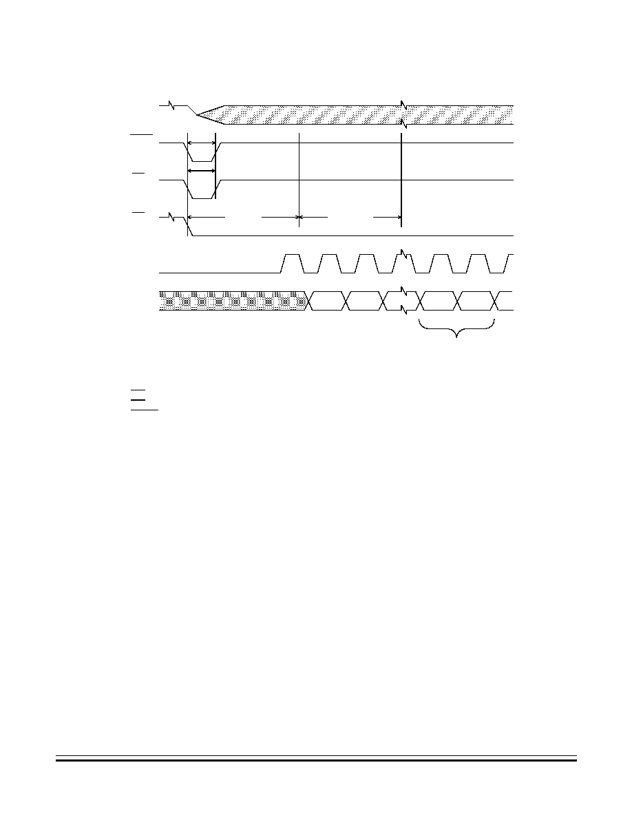
Electrical Specifications
3.3-Volt Control Timing
MC68HC705C8A -- Rev. 3
Technical Data
MOTOROLA
Electrical Specifications
183
Figure 13-6. Stop Recovery Timing Diagram
1FFE
1FFE
1FFE
1FFE
1FFF
(4)
t
ILCH
4064 t
CYC
t
ILIH
t
RL
Notes:
1. Represents the internal gating of the OSC1 pin
2. IRQ pin edge-sensitive option
3. IRQ pin level and edge-sensitive option
4. RESET vector address shown for timing example
RESET OR INTERRUPT
VECTOR FETCH
OSC1
(1)
RESET
IRQ
(2)
IRQ
(3)
INTERNAL
CLOCK
INTERNAL
ADDRESS
BUS
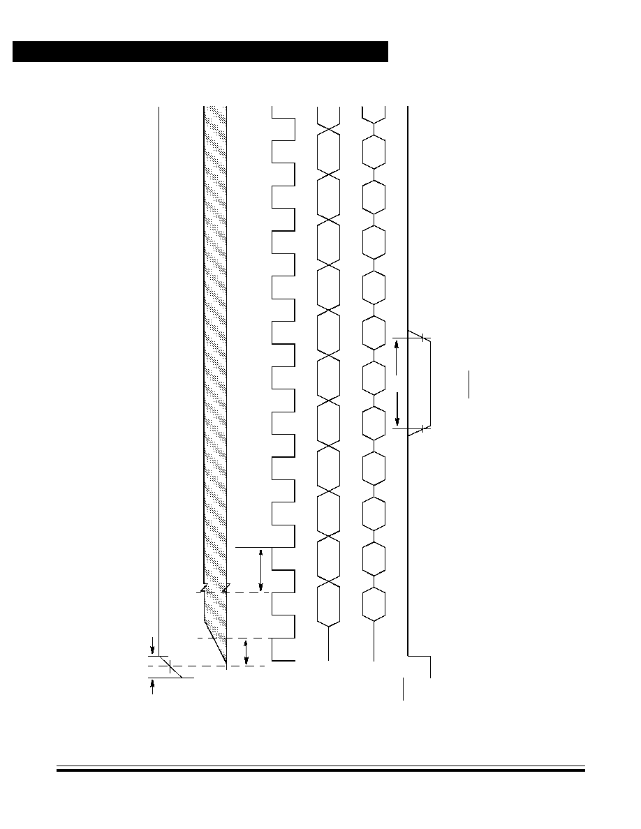
T
e
c
hni
c
a
l
Dat
a
M
C
68HC7
05C8A
--
Rev
.
3
184
E
l
ec
t
r
i
c
al
S
pec
i
f
i
c
at
i
ons
M
O
T
O
ROLA
Ele
c
t
r
ica
l
Sp
ec
if
ica
t
ions
Figure 13-7. Power-On Reset and External Reset Timing Diagram
PCH
PCL
OSC1
RESET
INTERNAL
PROCESSOR
INTERNAL
ADDRESS
BUS
1FFE
1FFF
V
DD
V
DD
THRESHOLD (1-2 V TYPICAL)
t
VDDR
t
RL
INTERNAL
DATA
BUS
1FFE
1FFE
1FFE
1FFE
NEW PC
1FFF
*
OSC1 line is not meant to represent frequency. It is only used to represent time.
**
Internal timing signal and bus information are not available externally.
***
The next rising edge of the internal processor clock following the rising edge of RESET initiates the reset sequence.
NEW
NEW
PCL
PCH
NEW PC
CLOCK
OP
CODE
OP
CODE
t
CYC
t
OXOV
*
* *
*
**
***

Electrical Specifications
5.0-Volt Serial Peripheral Interface (SPI) Timing
MC68HC705C8A -- Rev. 3
Technical Data
MOTOROLA
Electrical Specifications
185
13.11
5.0-Volt Serial Peripheral Interface (SPI) Timing
Number
(1)
Characteristic
(2)
Symbol
Min
Max
Unit
Operating frequency
Master
Slave
f
OP(M)
f
OP(S)
dc
dc
0.5
2.1
f
OP
MHz
1
Cycle time
Master
Slave
t
CYC(M)
t
CYC(S)
2.0
480
--
--
t
CYC
ns
2
Enable lead time
Master
Slave
t
Lead(M)
t
Lead(S)
(3)
240
--
--
ns
3
Enable lag time
Master
Slave
t
Lag(M)
t
Lag(S)
(2)
720
--
--
ns
4
Clock (SCK) high time
Master
Slave
t
W(SCKH)M
t
W(SCKH)S
340
190
--
--
ns
5
Clock (SCK) low time
Master
Slave
t
W(SCKL)M
t
W(SCKL)S
340
190
--
--
ns
6
Data setup time (inputs)
Master
Slave
t
SU(M)
t
SU(S)
100
100
--
--
ns
7
Data hold time (inputs)
Master
Slave
t
H(M)
t
H(S)
100
100
--
--
ns
8
Access time
(4)
Slave
t
A
0
120
ns
9
Disable time
(5)
Slave
t
DIS
--
240
ns
10
Data valid time
Master (before capture edge)
Slave (after enable edge)
(6)
t
V(M)
t
V(S)
0.25
--
--
240
t
CYC(M)
ns
Continued

Technical Data
MC68HC705C8A -- Rev. 3
186
Electrical Specifications
MOTOROLA
Electrical Specifications
11
Data hold time (outputs)
Master (after capture edge)
Slave (after enable edge)
t
HO(M)
t
HO(S)
0.25
0
--
--
t
CYC(M)
ns
12
Rise time
(7)
SPI outputs (SCK, MOSI, MISO)
SPI inputs (SCK, MOSI, MISO, SS)
t
R(M)
t
R(S)
--
--
100
2.0
ns
µ
s
13
Fall time
(8)
SPI outputs (SCK, MOSI, MISO)
SPI inputs (SCK, MOSI, MISO, SS)
t
F(M)
t
F(S)
--
--
100
2.0
ns
µ
s
1. Numbers refer to dimensions in
Figure 13-8
and
Figure 13-9
.
2. V
DD
= 5.0 Vdc
±
10%
3. Signal production depends on software.
4. Time to data active from high-impedance state
5. Hold time to high-impedance state
6. With 200 pF on all SPI pins
7. 20% of V
DD
to 70% of V
DD
; C
L
= 200 pF
8. 70% of V
DD
to 20% of V
DD
; C
L
= 200 pF
Number
(1)
Characteristic
(2)
Symbol
Min
Max
Unit

Electrical Specifications
3.3-Volt Serial Peripheral Interface (SPI) Timing
MC68HC705C8A -- Rev. 3
Technical Data
MOTOROLA
Electrical Specifications
187
13.12
3.3-Volt Serial Peripheral Interface (SPI) Timing
Number
(1)
Characteristic
(2)
Symbol
Min
Max
Unit
Operating frequency
Master
Slave
f
OP(M)
f
OP(S)
dc
0.5
2.1
f
OP
MHz
1
Cycle time
Master
Slave
t
CYC(M)
t
CYC(S)
2.0
1
--
--
t
CYC
ns
2
Enable lead time
Master
Slave
t
Lead(M)
t
Lead(S)
(3)
500
--
--
ns
3
Enable lag time
Master
Slave
t
Lag(M)
t
Lag(S)
(2)
1500
--
--
ns
4
Clock (SCK) high time
Master
Slave
t
W(SCKH)M
t
W(SCKH)S
720
400
--
--
ns
5
Clock (SCK) low time
Master
Slave
t
W(SCKL)M
t
W(SCKL)S
720
400
--
--
ns
6
Data setup time (inputs)
Master
Slave
t
SU(M)
t
SU(S)
200
200
--
--
ns
7
Data hold time (inputs)
Master
Slave
t
H(M)
t
H(S)
200
200
--
--
ns
8
Access time
(4)
Slave
t
A
0
250
ns
9
Disable time
(5)
Slave
t
DIS
--
500
ns
10
Data valid time
Master (before capture edge)
Slave (after enable edge)
(6)
t
V(M)
t
V(S)
0.25
--
--
500
t
CYC(M)
ns
Continued

Technical Data
MC68HC705C8A -- Rev. 3
188
Electrical Specifications
MOTOROLA
Electrical Specifications
11
Data hold time (outputs)
Master (after capture edge)
Slave (after enable edge)
t
HO(M)
t
HO(S)
0.25
0
--
--
t
CYC(M)
ns
12
Rise time
(7)
SPI outputs (SCK, MOSI, MISO)
SPI inputs (SCK, MOSI, MISO, SS)
t
R(M)
t
R(S)
--
--
200
2.0
ns
µ
s
13
Fall time
(8)
SPI outputs (SCK, MOSI, MISO)
SPI inputs (SCK, MOSI, MISO, SS)
t
F(M)
t
F(S)
--
--
200
2.0
ns
µ
s
1. Numbers refer to dimensions in
Figure 13-8
and
Figure 13-9
.
2. V
DD
= 3.3 Vdc
±
10%
3. Signal production depends on software.
4. Time to data active from high-impedance state
5. Hold time to high-impedance state
6. With 200 pF on all SPI pins
7. 20% of V
DD
to 70% of V
DD
; C
L
= 200 pF
8. 70% of V
DD
to 20% of V
DD
; C
L
= 200 pF
Number
(1)
Characteristic
(2)
Symbol
Min
Max
Unit
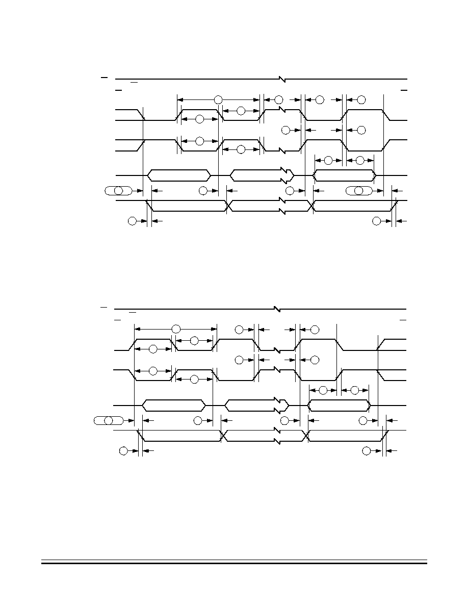
Electrical Specifications
3.3-Volt Serial Peripheral Interface (SPI) Timing
MC68HC705C8A -- Rev. 3
Technical Data
MOTOROLA
Electrical Specifications
189
Figure 13-8. SPI Master Timing
NOTE
Note: This first clock edge is generated internally, but is not seen at the SCK pin.
SS pin of master held high.
MSB IN
SS
INPUT
SCK (CPOL = 0)
OUTPUT
SCK (CPOL = 1)
OUTPUT
MISO
INPUT
MOSI
OUTPUT
NOTE
4
5
5
1
13
12
4
12
13
BITS 6≠1
LSB IN
MASTER MSB OUT
BITS 6≠1
MASTER LSB OUT
10
13
11
10
12
11
7
6
NOTE
Note: This last clock edge is generated internally, but is not seen at the SCK pin.
SS pin of master held high.
MSB IN
SS
INPUT
SCK (CPOL = 0)
OUTPUT
SCK (CPOL = 1)
OUTPUT
MISO
INPUT
MOSI
OUTPUT
NOTE
4
5
5
1
13
12
4
13
BITS 6≠1
LSB IN
MASTER MSB OUT
BITS 6≠1
MASTER LSB OUT
10
13
11
10
12
11
7
6
12
a) SPI Master Timing (CPHA = 0)
b) SPI Master Timing (CPHA = 1)
12

Technical Data
MC68HC705C8A -- Rev. 3
190
Electrical Specifications
MOTOROLA
Electrical Specifications
Figure 13-9. SPI Slave Timing
Note: Not defined, but normally MSB of character just received
SLAVE
SS
INPUT
SCK (CPOL = 0)
(INPUT
SCK (CPOL = 1)
INPUT
MISO
INPUT
MOSI
OUTPUT
4
5
5
1
13
12
4
13
MSB IN
BITS 6≠1
8
6
10
11
11
12
NOTE
SLAVE LSB OUT
9
3
LSB IN
2
7
BITS 6≠1
MSB OUT
Note: Not defined, but normally LSB of character previously transmitted
SLAVE
SS
INPUT
SCK (CPOL = 0)
INPUT
SCK (CPOL = 1)
INPUT
MISO
OUTPUT
MOSI
INPUT
4
5
5
1
13
12
4
13
MSB IN
BITS 6≠1
8
6
10
11
12
NOTE
SLAVE LSB OUT
9
3
LSB IN
2
7
BITS 6≠1
MSB OUT
10
a) SPI Slave Timing (CPHA = 0)
b) SPI Slave Timing (CPHA = 1)

MC68HC705C8A -- Rev. 3
Technical Data
MOTOROLA
Mechanical Specifications
191
Technical Data -- MC68HC705C8A
Section 14. Mechanical Specifications
14.1 Contents
14.2
Introduction . . . . . . . . . . . . . . . . . . . . . . . . . . . . . . . . . . . . . . . 191
14.3
40-Pin Plastic Dual In-Line Package (PDIP). . . . . . . . . . . . . .192
14.4
40-Pin Ceramic Dual In-Line Package (Cerdip) . . . . . . . . . . . 193
14.5
44-Lead Plastic-Leaded Chip Carrier (PLCC) . . . . . . . . . . . . 194
14.6
44-Lead Ceramic-Leaded Chip Carrier (CLCC) . . . . . . . . . . . 195
14.7
44-Pin Quad Flat Pack (QFP). . . . . . . . . . . . . . . . . . . . . . . . . 196
14.8
42-Pin Shrink Dual In-Line Package (SDIP) . . . . . . . . . . . . . .197
14.2 Introduction
Package dimensions available at the time of this publication for the
MC68HC705C8A are provided in this section. The packages are:
∑
40-pin plastic dual in-line package (PDIP)
∑
40-pin ceramic dual-in-line package (cerdip)
∑
44-lead plastic-leaded chip carrier (PLCC)
∑
44-lead ceramic-leaded chip carrier (CLCC)
∑
44-pin quad flat pack (QFP)
∑
42-pin shrink dual in-line package (SDIP)
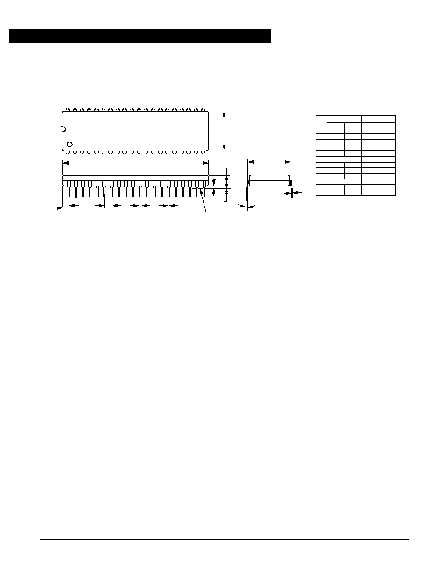
Technical Data
MC68HC705C8A -- Rev. 3
192
Mechanical Specifications
MOTOROLA
Mechanical Specifications
14.3 40-Pin Plastic Dual In-Line Package (PDIP)
Figure 14-1. MC68HC705C8AP Package Dimensions (Case #711)
1
20
40
21
B
A
C
SEATING
PLANE
D
F
G
H
K
N
M
J
L
DIM
MIN
MAX
MIN
MAX
INCHES
MILLIMETERS
A
51.69
52.45
2.035
2.065
B
13.72
14.22
0.540
0.560
C
3.94
5.08
0.155
0.200
D
0.36
0.56
0.014
0.022
F
1.02
1.52
0.040
0.060
G
2.54 BSC
0.100 BSC
H
1.65
2.16
0.065
0.085
J
0.20
0.38
0.008
0.015
K
2.92
3.43
0.115
0.135
L
15.24 BSC
0.600 BSC
M
1
∞
N
0.51
1.02
0.020
0.040
NOTES:
1.POSITION TOLERANCE OF LEADS (D), SHALL
BEWITHIN 0.25 (0.010) AT MAXIMUM MATERIAL
CONDITIONS, IN RELATION TO SEATING PLANE
AND EACH OTHER.
2.DIMENSION L TO CENTER OF LEADS WHEN
FORMED PARALLEL.
3.DIMENSION B DOES NOT INCLUDE MOLD FLASH.
1
∞
0
∞
0
∞

Mechanical Specifications
40-Pin Ceramic Dual In-Line Package (Cerdip)
MC68HC705C8A -- Rev. 3
Technical Data
MOTOROLA
Mechanical Specifications
193
14.4 40-Pin Ceramic Dual In-Line Package (Cerdip)
Figure 14-2. MC68HC705C8AS Package Dimensions (Case #734A)
M
L
J
DIM
MIN
MAX
MIN
MAX
MILLIMETERS
INCHES
A
2.020 2.096 51.31 53.23
B
0.500 0.610 12.70 15.94
C
0.160 0.240
4.06
6.09
D
0.015 0.022
0.38
0.55
F
0.050 0.065
1.27
1.65
G
0.100 BSC
2.54 BSC
J
0.008 0.012
0.20
0.30
K
0.125 0.160
3.17
4.06
L
0.600 BSC
15.24 BSC
M
0∞ 15∞
0∞ 15∞
N
0.020 0.050
0.51
1.27
A
0.25(0.010)
T
T
40 PL
D
1
40
20
21
A
B
G
F
K
C
N
SEATING
PLANE
DATUM
PLANE
M
M
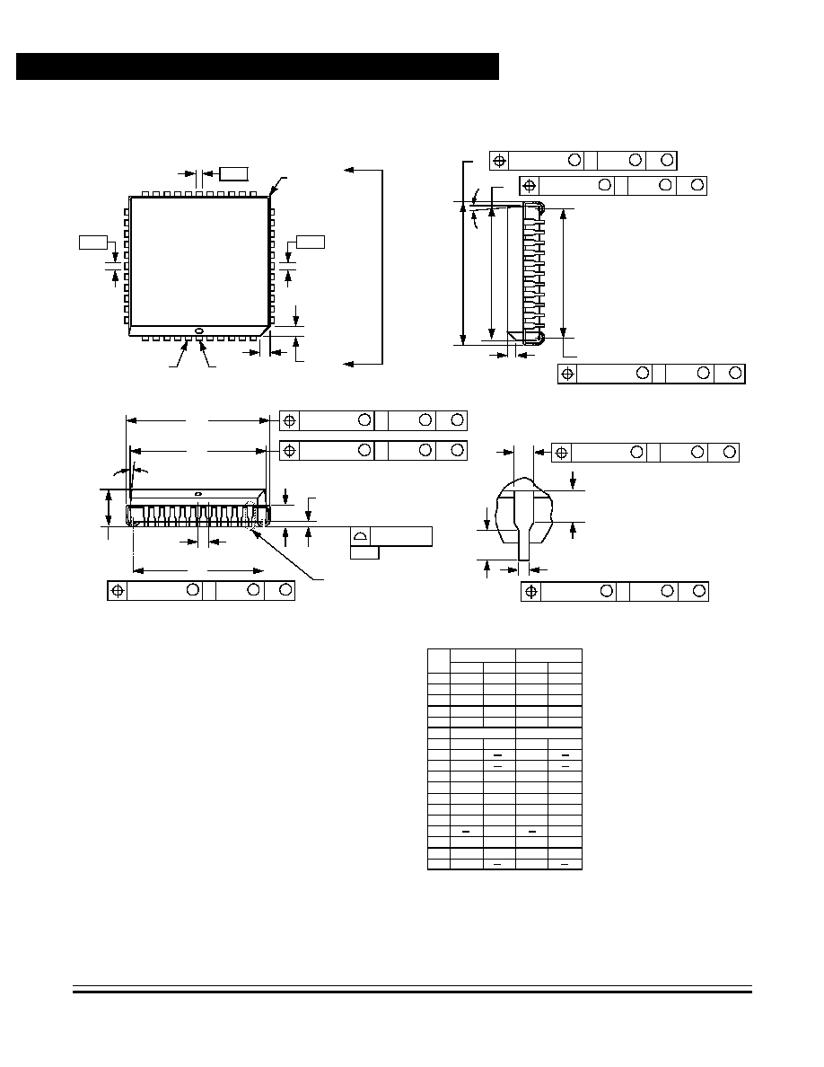
Technical Data
MC68HC705C8A -- Rev. 3
194
Mechanical Specifications
MOTOROLA
Mechanical Specifications
14.5 44-Lead Plastic-Leaded Chip Carrier (PLCC)
Figure 14-3. MC68HC705C8AFN Package Dimensions (Case #777)
-N-
-L-
-M-
D
Y
D
K
V
W
1
44
BRK
B
Z
U
X
VIEW D-D
S
L-M
M
0.007(0.180)
N S
T
S
L-M
M
0.007(0.180)
N S
T
G1
S
L-M
S
0.010 (0.25)
N S
T
K1
F
H
S
L-M
M
0.007(0.180)
N S
T
Z
G
G1
R
A
E
J
VIEW S
C
S
L-M
M
0.007(0.180)
N S
T
S
L-M
M
0.007(0.180)
N S
T
0.004 (0.10)
-T-
SEATING
PLANE
VIEW S
DIM
MIN
MAX
MIN
MAX
MILLIMETERS
INCHES
A
0.685
0.695
17.40
17.65
B
0.685
0.695
17.40
17.65
C
0.165
0.180
4.20
4.57
E
0.090
0.110
2.29
2.79
F
0.013
0.019
0.33
0.48
G
0.050 BSC
1.27 BSC
H
0.026
0.032
0.66
0.81
J
0.020
0.51
K
0.025
0.64
R
0.650
0.656
16.51
16.66
U
0.650
0.656
16.51
16.66
V
0.042
0.048
1.07
1.21
W
0.042
0.048
1.07
1.21
X
0.042
0.056
1.07
1.42
Y
0.020
0.50
Z
2
∞
10
∞
G1
0.610
0.630
15.50
16.00
K1
0.040
1.02
S
L-M
S
0.010 (0.25)
N S
T
S
L-M
M
0.007(0.180)
N S
T
2
∞
10
∞
NOTES:
1. DATUMS -L-, -M-, AND -N- ARE DETERMINED
WHERE TOP OF LEAD SHOLDERS EXITS
PLASTIC BODY AT MOLD PARTING LINE.
2. DIMENSION G1, TRUE POSITION TO BE
MEASURED AT DATUM -T-, SEATING PLANE.
3. DIMENSION R AND U DO NOT INCLUDE MOLD
FLASH. ALLOWABLE MOLD FLASH IS 0.010
(0.25) PER SIDE.
4. DIMENSIONING AND TOLERANCING PER ANSI
Y14.5M, 1982.
5. CONTROLLING DIMENSION: INCH.
6. THE PACKAGE TOP MAY BE SMALLER THAN
THE PACKAGE BOTTOM BY UP TO 0.012
(0.300). DIMENSIONS R AND U ARE DETERMINED
AT THE OUTERMOST EXTREMES OF THE
PLASTIC BODY EXCLUSIVE OF THE MOLD
FLASH, TIE BAR BURRS, GATE BURRS AND
INTERLEAD FLASH, BUT INCLUDING ANY
MISMATCH BETWEEN THE TOP AND BOTTOM
OF THE PLASTIC BODY.
7. DIMINSION H DOES NOT INCLUDE DAMBAR
PROTRUSION OR INTRUSION. THE DAMBAR
PROTUSION(S) SHALL NOT CAUSE THE H
DIMINSION TO BE GREATER THAN 0.037
(0.940198). THE DAMBAR INTRUSION(S) SHALL
NOT CAUSE THE H DIMINISION TO SMALLER
THAN 0.025 (0.635).
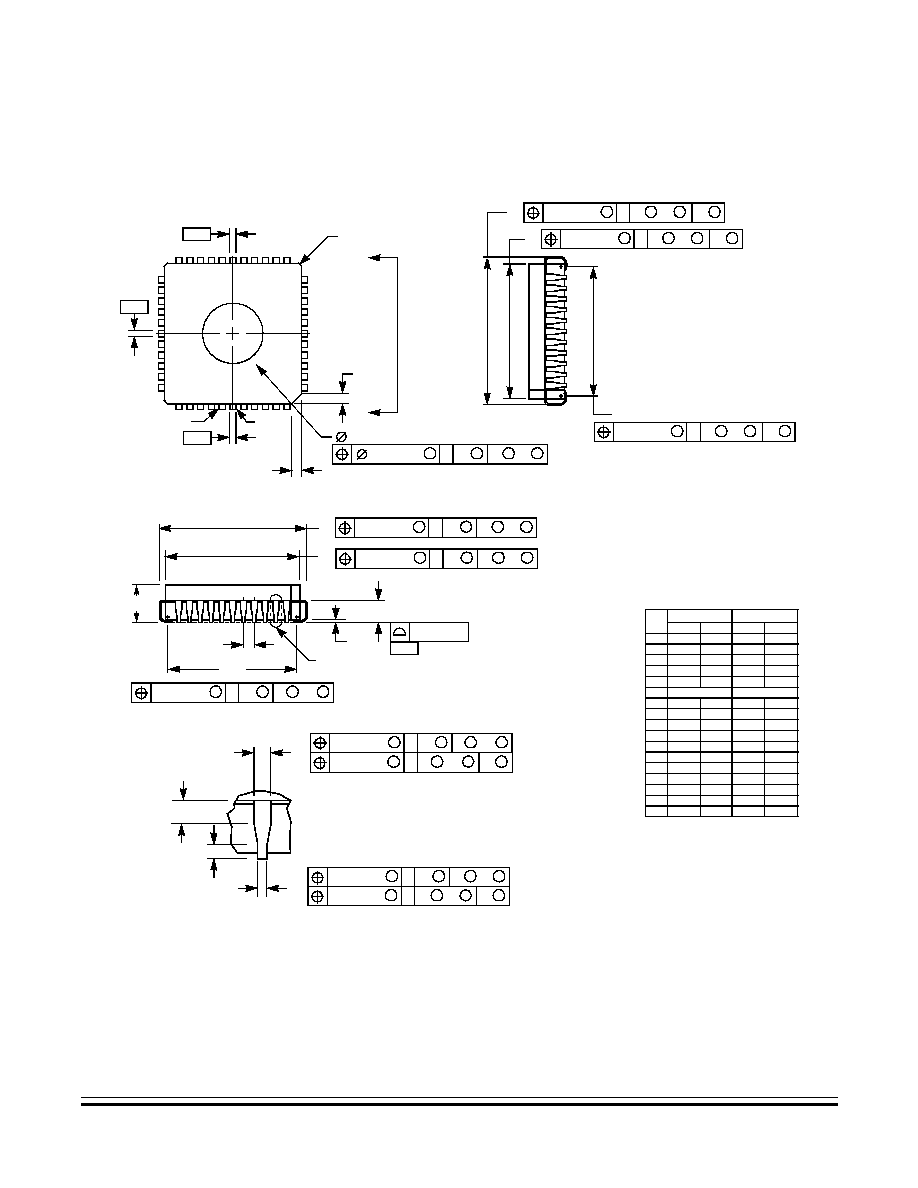
Mechanical Specifications
44-Lead Ceramic-Leaded Chip Carrier (CLCC)
MC68HC705C8A -- Rev. 3
Technical Data
MOTOROLA
Mechanical Specifications
195
14.6 44-Lead Ceramic-Leaded Chip Carrier (CLCC)
Figure 14-4. MC68HC705C8AFS Package Dimensions (Case #777B)
17.40
17.40
4.20
2.29
0.33
0.66
0.51
0.64
16.51
6.94
16.51
1.07
1.07
---
14.99
1.02
S
L
M
0.18 (0.007)
N -P
S
S
T
B
U
G1
S
L
M
0.18 (0.007)
N -P
S
S
T
S
L
M
N -P
S
S
T
DETAIL D-D
-N-
M
L
M
0.20 (0.008)
N -P
M
M
T
-L-
-P-
1
44
V
D
W
S
D
Y
BRK
S
L
M
0.18 (0.007)
N -P
S
S
T
S
L
M
0.18 (0.007)
N -P
S
S
T
0.10 (0.004)
SEATING
PLANE
-T-
J
E
R
A
G
G1
S
L
S
0.25 (0.010)
N -P
S
S
T
DETAIL S
C
S
L
M
0.18 (0.007)
N -P
S
S
T
S
L
M
0.18 (0.007)
N -P
S
S
T
F
S
L
M
0.18 (0.007)
N -P
S
S
T
S
L
M
0.18 (0.007)
N -P
S
S
T
H
K
K1
DETAIL S
DIM
MIN
MAX
MIN
MAX
INCHES
MILLIMETERS
A
17.65
0.685
0.695
B
17.65
0.685
0.695
C
4.57
0.165
0.180
E
2.79
0.090
0.110
F
0.48
0.013
0.019
G
1.27 BSC
0.050 BSC
H
0.81
0.026
0.032
J
---
0.020
---
K
---
0.025
---
R
16.66
0.650
0.656
S
7.26
0.273
0.286
U
16.66
0.650
0.656
V
1.21
0.042
0.048
W
1.21
0.042
0.048
Y
0.50
---
0.020
G1
16.00
0.590
0.630
K1
---
0.040
---
NOTES:
1. DATUMS -L-, -N-, AND -P- DETERMINED
WHERE TOP OF LEAD SHOULDER EXIT
BODY.
2. DIMINSION G1, TRUE POSITION TO BE
MEASURED AT DATUM -T-, SEATING
PLANE.
3. DIMINSIONS R AND U DO NOT INCLUDE
GLASS MENISCUS. ALLOWABLE GLASS
RUNOUT IS 0.25 (0.010) PER SIDE.
4. DIMINSIONING AND TOLERANCING PER
ANSI Y14.5M, 1982.
0.25 (0.010)
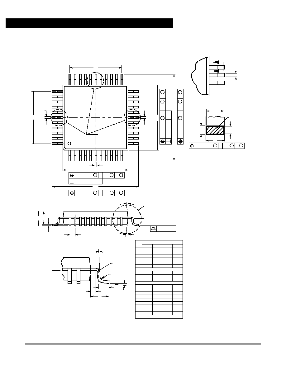
Technical Data
MC68HC705C8A -- Rev. 3
196
Mechanical Specifications
MOTOROLA
Mechanical Specifications
14.7 44-Pin Quad Flat Pack (QFP)
Figure 14-5. MC68HC705C8AFB Package Dimensions (Case #824A)
NOTES:
1.
1. DIMENSIONING AND TOLERANCING PER ANSI
Y14.5M, 1982.
2.
2. CONTROLLING DIMENSION: MILLIMETER.
3.
3. DATUM PLANE -H- IS LOCATED AT BOTTOM OF
LEAD AND IS COINCIDENT WITH THE LEAD WHERE
THE LEAD EXITS THE PLASTIC BODY AT THE
BOTTOM OF THE PARTING LINE.
4.
4. DATUMS -A-, -B- AND -D- TO BE DETERMINED AT
DATUM PLANE -H-.
5.
5. DIMENSIONS S AND V TO BE DETERMINED AT
SEATING PLANE -C-.
6.
6. DIMENSIONS A AND B DO NOT INCLUDE MOLD
PROTRUSION. ALLOWABLE PROTRUSION IS 0.25
(0.010) PER SIDE. DIMENSIONS A AND B DO
INCLUDE MOLD MISMATCH AND ARE DETERMINED
AT DATUM PLANE -H-.
7.
7. DIMENSION D DOES NOT INCLUDE DAMBAR
PROTRUSION. ALLOWABLE DAMBAR
PROTRUSION SHALL BE 0.08 (0.003) TOTAL IN
EXCESS OF THE D DIMENSION AT MAXIMUM
MATERIAL CONDITION. DAMBAR CANNOT BE
LOCATED ON THE LOWER RADIUS OR THE FOOT.
L
33
34
23
22
44
1
11
12
DETAIL A
-D-
-A-
A
S
A-B
M
0.20 (0.008)
D
S
C
S
A-B
M
0.20 (0.008)
D
S
H
0.05 (0.002) A-B
S
B
S
A-B
M
0.
20 (
0
.
0
0
8
)
D
S
C
S
A-B
M
0.
20
(
0
.
0
08)
D
S
H
0.
05
(
0
.
0
0
2
)
A-B
V
L
-B-
-C-
SEATING
PLANE
M
M
E
H
G
C
-H-
DATUM
PLANE
DETAIL C
0.01 (0.004)
M
-H-
DATUM
PLANE
T
R
K
Q
W
X
DETAIL C
DIM
MIN
MAX
MIN
MAX
INCHES
MILLIMETERS
A
9.90
10.10
0.390
0.398
B
9.90
10.10
0.390
0.398
C
2.10
2.45
0.083
0.096
D
0.30
0.45
0.012
0.018
E
2.00
2.10
0.079
0.083
F
0.30
0.40
0.012
0.016
G
0.80 BSC
0.031 BSC
H
---
0.25
---
0.010
J
0.013
0.23
0.005
0.009
K
0.65
0.95
0.026
0.037
L
8.00 REF
0.315 REF
M
5
10
5
10
N
0.13
0.17
0.005
0.007
Q
0
7
0
7
R
0.13
0.30
0.005
0.012
S
12.95
13.45
0.510
0.530
T
0.13
---
0.005
---
U
0
---
0
---
V
12.95
13.45
0.510
0.530
W
0.40
---
0.016
---
X
1.6 REF
0.063 REF
DETAIL A
B
B
-A-, -B-, -D-
S
A-B
M
0.20 (0.008)
D
S
C
F
N
SECTION B-B
J
D
BASE METAL
∞
∞
∞
∞
∞
∞
∞
∞
∞
∞
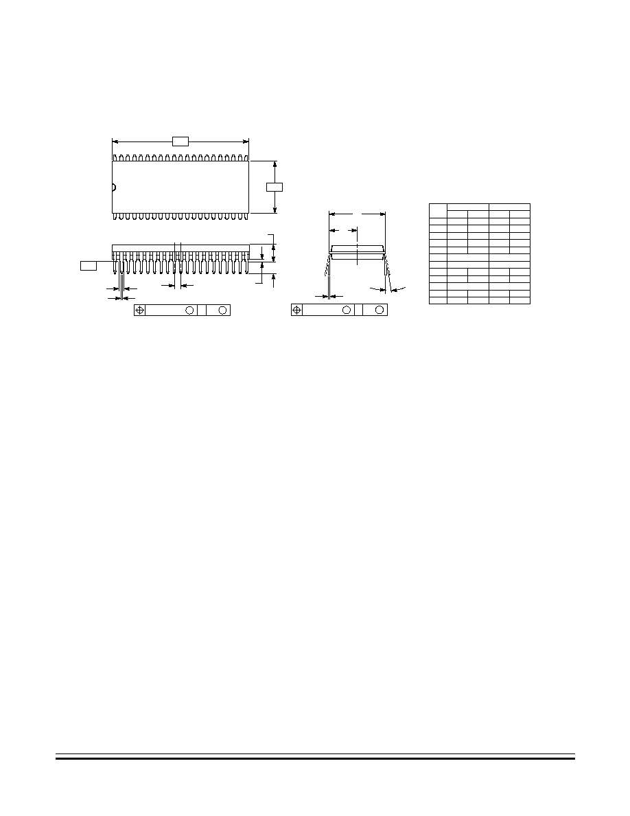
Mechanical Specifications
42-Pin Shrink Dual In-Line Package (SDIP)
MC68HC705C8A -- Rev. 3
Technical Data
MOTOROLA
Mechanical Specifications
197
14.8 42-Pin Shrink Dual In-Line Package (SDIP)
Figure 14-6. MC68HC705C8AB Package Dimensions (Case #858)
1.435
0.540
0.155
0.014
0.032
0.008
0.115
0
∞
0.020
1.465
0.560
0.200
0.022
0.046
0.015
0.135
15
∞
0.040
37.21
14.22
5.08
0.56
1.17
0.38
3.43
15
∞
1.02
36.45
13.72
3.94
0.36
0.81
0.20
2.92
0
∞
0.51
-B-
-A-
C
D
42 PL
F
K
G
N
J
42 PL
M
MIN
MIN
MAX
MAX
INCHES
MILLIMETERS
DIM
A
B
C
D
F
G
H
J
K
L
M
N
H
L
1.778 BSC
0.070 BSC
7.62 BSC
0.300 BSC
15.24 BSC
0.600 BSC
0.25 (0.010)
T A
M
S
0.25 (0.010)
T B
M
S
NOTES:
1. DIMENSIONS AND TOLERANCING PER ANSI
Y14.5M, 1982.
2. CONTROLLING DIMENSION: INCH.
3. DIMENSION L TO CENTER OF LEAD WHEN
FORMED PARALLEL.
4. DIMENSIONS A AND B DO NOT INCLUDE MOLD
FLASH. MAXIMUM MOLD FLASH 0.25 (0.010).
1
21
42
22
SEATING
PLANE
-T-

Technical Data
MC68HC705C8A -- Rev. 3
198
Mechanical Specifications
MOTOROLA
Mechanical Specifications
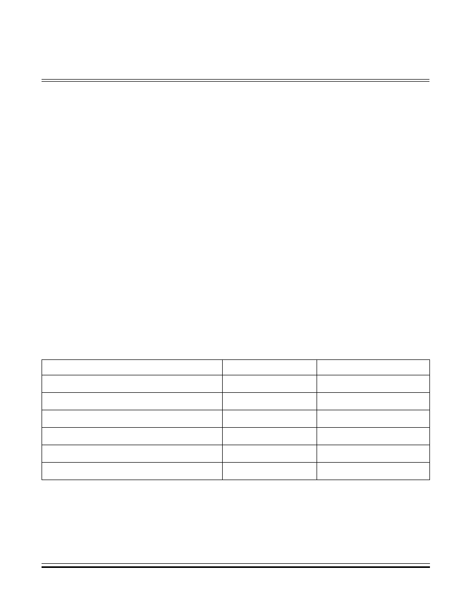
MC68HC705C8A -- Rev. 3
Technical Data
MOTOROLA
Ordering Information
199
Technical Data -- MC68HC705C8A
Section 15. Ordering Information
15.1 Contents
15.2
Introduction . . . . . . . . . . . . . . . . . . . . . . . . . . . . . . . . . . . . . . . 199
15.3
MCU Order Numbers . . . . . . . . . . . . . . . . . . . . . . . . . . . . . . . 199
15.2 Introduction
This section contains ordering information for the available package
types.
15.3 MCU Order Numbers
Table 15-1
lists the MC order numbers.
Table 15-1. MC68HC705C8A Order Numbers
Package Type
Temperature Range
Order Number
40-pin plastic dual in-line package (PDIP)
≠40
∞
C to +85
∞
C
MC68HC705C8AC
(1)
P
(2)
44-lead plastic-leaded chip carrier (PLCC)
≠40
∞
C to +85
∞
C
MC68HC705C8ACFN
(3)
44-lead ceramic-leaded chip carrier (CLCC)
≠40
∞
C to +85
∞
C
MC68HC705C8ACFS
(4)
40-pin windowed ceramic DIP (Cerdip)
≠40
∞
C to +85
∞
C
MC68HC705C8ACS
(5)
44-pin quad flat pack (QFP)
≠40
∞
C to +85
∞
C
MC68HC705C8ACFB
(6)
42-pin shrink dual in-line package (SDIP)
≠40
∞
C to +85
∞
C
MC68HC705C8ACB
(7)
1. C = Extended temperature range (≠40
∞
C to +85
∞
C)
2. P = Plastic dual in-line package (PDIP)
3. FN = Plastic-leaded chip carrier (PLCC)
4. FS = Ceramic-leaded chip carrier (CLCC)
5. S = Windowed ceramic dual in-line package (Cerdip)
6. FB = Quad flat pack (QFP)
7. B = Shrink dual in-line package (SDIP)

Technical Data
MC68HC705C8A -- Rev. 3
200
Ordering Information
MOTOROLA
Ordering Information

MC68HC705C8A -- Rev. 3
Technical Data
MOTOROLA
MC68HSC705C8A
201
Technical Data -- MC68HC705C8A
Appendix A. MC68HSC705C8A
A.1 Contents
A.2
Introduction . . . . . . . . . . . . . . . . . . . . . . . . . . . . . . . . . . . . . . . 201
A.3
5.0-Volt High-Speed DC Electrical Characteristics. . . . . . . . .202
A.4
3.3-Volt High-Speed DC Electrical Characteristics . . . . . . . . 203
A.5
5.0-Volt High-Speed Control Timing . . . . . . . . . . . . . . . . . . . . 204
A.6
3.3-Volt High-Speed Control Timing . . . . . . . . . . . . . . . . . . . . 204
A.7
5.0-Volt High-Speed SPI Timing . . . . . . . . . . . . . . . . . . . . . . 205
A.8
3.3-Volt High-Speed SPI Timing. . . . . . . . . . . . . . . . . . . . . . .207
A.9
Ordering Information. . . . . . . . . . . . . . . . . . . . . . . . . . . . . . . . 209
A.2 Introduction
The MC68HSC705C8A is an enhanced, high-speed version of the
MC68HC705C8A, featuring a 4-MHz bus speed.
The data in this document, MC68HC705C8A Technical Data Rev. 3,
applies to the MC68HSC705C8A with the exceptions given in this
appendix.
The computer operating properly (COP) mode bits (CM1 and CM0 in the
COP control register) select the timeout period of the programmable
COP watchdog, as shown in
Table A-1
. See
Figure 5-3.
Programmable COP Control Register (COPCR)
.
Technical Data
MC68HC705C8A -- Rev. 3
202
MC68HSC705C8A
MOTOROLA
MC68HSC705C8A
A.3 5.0-Volt High-Speed DC Electrical Characteristics
Table A-1. Programmable COP Timeout Period Selection
CM1:CM0
COP
Timeout
Rate
Programmable COP Timeout Period
f
OSC
= 8.0 MHz
f
OP
= 4.0 MHz
f
OSC
= 4.0 MHz
f
OP
= 2.0 MHz
f
OSC
= 3.5795 MHz
f
OP
= 1.7897 MHz
f
OSC
= 2.0 MHz
f
OP
= 1.0 MHz
00
f
OP
˜
2
15
8.192 ms
16.38 ms
18.31 ms
32.77 ms
01
f
OP
˜
2
17
32.77 ms
65.54 ms
73.24 ms
131.07 ms
10
f
OP
˜
2
19
131.07 ms
262.14 ms
292.95 ms
524.29 ms
11
f
OP
˜
˜2
21
524.29 ms
1.048 s
1.172 s
2.097 s
Characteristic
(1)
1. V
DD
= 5 V
±
10%; V
SS
= 0 Vdc, T
A
= T
L
to T
H
, unless otherwise noted
Symbol
Min
Typ
(2)
2. Typical values reflect average measurements at midpoint of voltage range at 25
∞
C.
Max
Unit
Output high voltage
I
Load
= ≠0.8 mA
PA7≠PA0, PB7≠PB0, PC6≠PC0, TCMP
I
Load
= ≠1.6 mA
PD4≠PD1
I
Load
= ≠5.0 mA
PC7
V
OH
V
DD
≠ 0.8
--
--
--
--
--
--
V
Output low voltage
I
Load
= 1.6 mA
PA7≠PA0, PB7≠PB0, PC6≠PC0, PD4≠PD1
I
Load
= 20 mA
PC7
V
OL
--
--
--
--
0.4
0.4
V
Supply current
(3)
Run
(4)
Wait
(5)
Stop
(6)
25
∞
C
≠40
∞
C to +85
∞
C
3. I
DD
measured with port B pullup devices disabled.
4. Run (operating) I
DD
measured using external square wave clock source (f
OSC
= 8.0 MHz). All inputs 0.2 V from rail. No dc
loads. Less than 50 pF on all outputs. C
L
= 20 pF on OSC2. OSC2 capacitance linearly affects run I
DD
.
5. Wait I
DD
measured using external square wave clock source (f
OSC
= 8.0 MHz). All inputs 0.2 V from rail. No dc loads. Less
than 50 pF on all outputs. C
L
= 20 pF on OSC2. V
IL
= 0.2 V, V
IH
= V
DD
≠ 0.2 V. All ports configured as inputs. SPI and SCI
disabled. If SPI and SCI enabled, add 10% current draw. OSC2 capacitance linearly affects wait I
DD
.
6. Stop I
DD
measured with OSC1 = V
DD
. All ports configured as inputs. V
IL
= 0.2 V, V
IH
= V
DD
≠ 0.2 V.
I
DD
--
--
--
--
5.92
2.27
5
2.0
14
7.0
50
50
mA
mA
µ
A
µ
A

MC68HSC705C8A
MC68HC705C8A -- Rev. 3
Technical Data
MOTOROLA
MC68HSC705C8A
203
A.4 3.3-Volt High-Speed DC Electrical Characteristics
Characteristic
(1)
1. V
DD
= 3.3 V
±
10%; V
SS
= 0 Vdc, T
A
= T
L
to T
H
, unless otherwise noted
Symbol
Min
Typ
(2)
2. Typical values reflect average measurements at midpoint of voltage range at 25
∞
C.
Max
Unit
Output high voltage
I
Load
= ≠0.2 mA
PA7≠PA0, PB7≠PB0, PC6≠PC0, TCMP
I
Load
= ≠0.4 mA
PD4≠PD1
I
Load
= ≠1.5 mA
PC7
V
OH
V
DD
≠ 0.3
--
--
--
--
--
--
V
Output low voltage
I
Load
= 0.4 mA
PA7≠PA0, PB7≠PB0, PC6≠PC0, PD4≠PD1
I
Load
= 6.0 mA
PC7
V
OL
--
--
--
--
0.3
0.3
V
Supply current
(3)
Run
(4)
Wait
(5)
Stop
(6)
3. I
DD
measured with port B pullup devices disabled.
4. Run (operating) I
DD
measured using external square wave clock source (f
OSC
= 4.2 MHz). All inputs 0.2 V from rail. No dc
loads. Less than 50 pF on all outputs. C
L
= 20 pF on OSC2. OSC2 capacitance linearly affects run I
DD
.
5. Wait I
DD
measured using external square wave clock source (f
OSC
= 4.2 MHz). All inputs 0.2 V from rail. No dc loads. Less
than 50 pF on all outputs. C
L
= 20 pF on OSC2. V
IL
= 0.2 V, V
IH
= V
DD
≠ 0.2 V. All ports configured as inputs. SPI and SCI
disabled. If SPI and SCI enabled, add 10% current draw. OSC2 capacitance linearly affects wait I
DD
.
6. Stop I
DD
measured with OSC1 = V
DD
. All ports configured as inputs. V
IL
= 0.2 V; V
IH
= V
DD
≠ 0.2 V.
I
DD
--
--
--
1.91
0.915
2.0
6.0
2.0
20
mA
mA
µ
A

Technical Data
MC68HC705C8A -- Rev. 3
204
MC68HSC705C8A
MOTOROLA
MC68HSC705C8A
A.5 5.0-Volt High-Speed Control Timing
A.6 3.3-Volt High-Speed Control Timing
Characteristic
(1)
Symbol
Min
Max
Unit
Oscillator frequency
Crystal oscillator
External clock
f
OSC
--
dc
8.0
8.0
MHz
Internal operating frequency (f
OSC
˜
2)
Crystal oscillator
External clock
f
OP
--
dc
4.0
4.0
MHz
Cycle time
t
CYC
250
--
ns
Input capture pulse width
t
TH
, t
TL
65
--
ns
Interrupt pulse width low (edge-triggered)
t
ILIH
65
--
ns
OSC1 pulse width
t
OH
, t
OL
45
--
ns
1. V
DD
= 5 V
±
10%; V
SS
= 0 Vdc, T
A
= T
L
to T
H
, unless otherwise noted
Characteristic
(1)
Symbol
Min
Max
Unit
Oscillator frequency
Crystal oscillator
External clock
f
OSC
--
dc
4.0
4.0
MHz
Internal operating frequency (f
OSC
˜
2)
Crystal oscillator
External clock
f
OP
--
dc
2.0
2.0
MHz
Cycle time
t
CYC
476
--
ns
Input capture pulse width
t
TH
, t
TL
125
--
ns
Interrupt pulse width low (edge-triggered)
t
ILIH
125
--
ns
OSC1 pulse width
t
OH
, t
OL
90
--
ns
1. V
DD
= 3.3 V
±
10%; V
SS
= 0 Vdc, T
A
= T
L
to T
H
, unless otherwise noted

MC68HSC705C8A
MC68HC705C8A -- Rev. 3
Technical Data
MOTOROLA
MC68HSC705C8A
205
A.7 5.0-Volt High-Speed SPI Timing
Diagram
Number
(1)
Characteristic
(2)
Symbol
Min
Max
Unit
Operating frequency
Master
Slave
f
OP(S)
f
OP(S)
dc
dc
0.5
4.0
f
OP
MHz
1
Cycle time
Master
Slave
t
CYC(M)
t
CYC(S)
2.0
250
--
--
t
CYC
ns
2
Enable lead time
Master
Slave
t
Lead(M)
t
Lead(S)
Note
(3)
125
--
--
ns
3
Enable lag time
Master
Slave
t
Lag(M)
t
Lag(S)
Note
(2)
375
--
--
ns
4
Clock (SCK) high time
Master
Slave
t
W(SCKH)M
t
W(SCKH)S
170
95
--
--
ns
5
Clock (SCK) low time
Master
Slave
t
W(SCKL)M
t
W(SCKL)S
170
95
--
--
ns
6
Data setup time (inputs)
Master
Slave
t
SU(M)
t
SU(S)
50
50
--
--
ns
7
Data hold time (inputs)
Master
Slave
t
H(M)
t
H(S)
50
50
--
--
ns
8
Access time
(4)
Slave
t
A
0
60
ns
9
Disable time
(5)
Slave
t
DIS
--
120
ns
10
Data valid time
Master (before capture edge)
Slave (after enable edge)
(6)
t
V(M)
t
V(S)
0.25
--
--
120
t
CYC(M)
ns
Continued

Technical Data
MC68HC705C8A -- Rev. 3
206
MC68HSC705C8A
MOTOROLA
MC68HSC705C8A
11
Data hold time (outputs)
Master (after capture edge)
Slave (after enable edge)
t
HO(M)
t
HO(S)
0.25
0
--
--
t
CYC(M)
ns
12
Rise time
(7)
SPI outputs (SCK, MOSI, MISO)
SPI inputs (SCK, MOSI, MISO, SS)
t
RM
t
RS
--
--
50
2.0
ns
µ
s
13
Fall time
(8)
SPI outputs (SCK, MOSI, MISO)
SPI inputs (SCK, MOSI, MISO, SS)
t
FM
t
FS
--
--
50
2.0
ns
µ
s
1. Diagram numbers refer to dimensions in
Figure 13-8. SPI Master Timing
and
Figure 13-9. SPI Slave Timing
.
2. V
DD
= 5 V
±
10%; V
SS
= 0 Vdc, T
A
= T
L
to T
H
, unless otherwise noted
3. Signal production depends on software.
4. Time to data active from high-impedance state
5. Hold time to high-impedance state
6. With 200 pF on all SPI pins.
7. 20% of V
DD
to 70% of V
DD
; C
L
= 200 pF
8. 70% of V
DD
to 20% of V
DD
; C
L
= 200 pF
Diagram
Number
(1)
Characteristic
(2)
Symbol
Min
Max
Unit

MC68HSC705C8A
MC68HC705C8A -- Rev. 3
Technical Data
MOTOROLA
MC68HSC705C8A
207
A.8 3.3-Volt High-Speed SPI Timing
Diagram
Number
(1)
Characteristic
(2)
Symbol
Min
Max
Unit
Operating frequency
Master
Slave
f
OP(S)
f
OP(S)
dc
dc
0.5
2.1
f
OP
MHz
1
Cycle time
Master
Slave
t
CYC(M)
t
CYC(S)
2.0
480
--
--
t
CYC
ns
2
Enable lead time
Master
Slave
t
Lead(M)
t
Lead(S)
Note
(3)
240
--
--
ns
3
Enable lag time
Master
Slave
t
Lag(M)
t
Lag(S)
Note
(2)
720
--
--
ns
4
Clock (SCK) high time
Master
Slave
t
W(SCKH)M
t
W(SCKH)S
340
190
--
--
ns
5
Clock (SCK) low time
Master
Slave
t
W(SCKL)M
t
W(SCKL)S
340
190
--
--
ns
6
Data setup time (inputs)
Master
Slave
t
SU(M)
t
SU(S)
100
100
--
--
ns
7
Data hold time (inputs)
Master
Slave
t
H(M)
t
H(S)
100
100
--
--
ns
8
Access time
(4)
Slave
t
A
0
120
ns
9
Disable time
(5)
Slave
t
DIS
--
240
ns
10
Data valid time
Master (before capture edge)
Slave (after enable edge)
(6)
t
V(M)
t
V(S)
0.25
--
--
240
t
CYC(M)
ns
Continued

Technical Data
MC68HC705C8A -- Rev. 3
208
MC68HSC705C8A
MOTOROLA
MC68HSC705C8A
11
Data hold time (outputs)
Master (after capture edge)
Slave (after enable edge)
t
HO(M)
t
HO(S)
0.25
0
--
--
t
CYC(M)
ns
12
Rise time
(7)
SPI outputs (SCK, MOSI, MISO)
SPI inputs (SCK, MOSI, MISO, SS)
t
RM
t
RS
--
--
100
2.0
ns
µ
s
13
Fall time
(8)
SPI outputs (SCK, MOSI, MISO)
SPI inputs (SCK, MOSI, MISO, SS)
t
FM
t
FS
--
--
100
2.0
ns
µ
s
1. Diagram numbers refer to dimensions in
Figure 13-8. SPI Master Timing
and
Figure 13-9. SPI Slave Timing
.
2. V
DD
= 3.3 V
±
10%; V
SS
= 0 Vdc, T
A
= T
L
to T
H
, unless otherwise noted
3. Signal production depends on software.
4. Time to data active from high-impedance state
5. Hold time to high-impedance state
6. With 200 pF on all SPI pins
7. 20% of V
DD
to 70% of V
DD
; C
L
= 200 pF
8. 70% of V
DD
to 20% of V
DD
; C
L
= 200 pF
Diagram
Number
(1)
Characteristic
(2)
Symbol
Min
Max
Unit
MC68HSC705C8A
MC68HC705C8A -- Rev. 3
Technical Data
MOTOROLA
MC68HSC705C8A
209
A.9 Ordering Information
Table A-2
provides ordering information for the MC68HSC705C8A.
Table A-2. MC68HSC705C8A Order Numbers
Package Type
Temperature Range
Order Number
40-pin plastic dual in-line package (PDIP)
≠40
∞
C to +85
∞
C
MC68HSC705C8AC
(1)
P
(2)
44-lead plastic-leaded chip carrier (PLCC)
≠40
∞
C to +85
∞
C
MC68HSC705C8ACFN
(3)
44-lead ceramic-leaded chip carrier (CLCC)
≠40
∞
C to +85
∞
C
MC68HSC705C8ACFS
(4)
40-pin ceramic DIP (cerdip)
≠40
∞
C to +85
∞
C
MC68HSC705C8ACS
(5)
44-pin quad flat pack (QFP)
≠40
∞
C to +85
∞
C
MC68HSC705C8ACFB
(6)
42-pin shrink dual in-line package (SDIP)
≠40
∞
C to +85
∞
C
MC68HSC705C8ACB
(7)
1. C = Extended temperature range (≠40
∞
C to +85
∞
C)
2. P = Plastic dual in-line package (PDIP)
3. FN = Plastic-leaded chip carrier (PLCC)
4. FS = Ceramic-leaded chip carrier (CLCC)
5. S = Windowed ceramic dual in-line package (cerdip)
6. FB = Quad flat pack (QFP)
7. B = Shrink dual in-line package (SDIP)

Technical Data
MC68HC705C8A -- Rev. 3
210
MC68HSC705C8A
MOTOROLA
MC68HSC705C8A

MC68HC705C8A -- Rev. 3
Technical Data
MOTOROLA
Index
211
Technical Data -- MC68HC705C8A
Index
A
accumulator (A)
. . . . . . . . . . . . . . . . . . . . . . . . . . . . . 45, 154, 155, 158
addressing modes
. . . . . . . . . . . . . . . . . . . . . . . . . . . . . . . . . . . . . . 154
arithmetic/logic unit (ALU)
. . . . . . . . . . . . . . . . . . . . . . . . . . . . . . . . . 48
B
block diagram
. . . . . . . . . . . . . . . . . . . . . . . . . . . . . . . . . . . . . . . . . . 24
bootloader ROM
. . . . . . . . . . . . . . . . . . . . . . . . . . . . . . . . . . . . . . . . 37
C
C bit
. . . . . . . . . . . . . . . . . . . . . . . . . . . . . . . . . . . . . . . . . . . . . . . . . 160
condition code register (CCR)
. . . . . . . . . . . . . . . . . . . . . . . . . . 47, 160
COP watchdog (non-programmable)
diagram
. . . . . . . . . . . . . . . . . . . . . . . . . . . . . . . . . . . . . . . . . . . . 67
flowchart
. . . . . . . . . . . . . . . . . . . . . . . . . . . . . . . . . . . . . . . . . . . . 73
in stop mode
. . . . . . . . . . . . . . . . . . . . . . . . . . . . . . . . . . . . . . . . . 73
reset
. . . . . . . . . . . . . . . . . . . . . . . . . . . . . . . . . . . . . . . . . . . . . . . 66
timeout period formula
. . . . . . . . . . . . . . . . . . . . . . . . . . . . . . . . . 66
when clock monitor enabled
. . . . . . . . . . . . . . . . . . . . . . . . . . . . . 73
COP watchdog (programmable)
COP control register (COPCR)
. . . . . . . . . . . . . . . . . . . . . . . . . . 64
COP reset register (COPRST)
. . . . . . . . . . . . . . . . . . . . . . . . . . . 64
diagram
. . . . . . . . . . . . . . . . . . . . . . . . . . . . . . . . . . . . . . . . . . . . 63
flowchart
. . . . . . . . . . . . . . . . . . . . . . . . . . . . . . . . . . . . . . . . . . . . 71
in stop mode
. . . . . . . . . . . . . . . . . . . . . . . . . . . . . . . . . . . . . . . . . 71
reset
. . . . . . . . . . . . . . . . . . . . . . . . . . . . . . . . . . . . . . . . . . . . . . . 63
timeout period selection
. . . . . . . . . . . . . . . . . . . . . . . . . . . . . . . . 66

Technical Data
MC68HC705C8A -- Rev. 3
212
Index
MOTOROLA
Index
CPU
instruction set summary
. . . . . . . . . . . . . . . . . . . . . . . . . . . . . . . 164
instruction types
. . . . . . . . . . . . . . . . . . . . . . . . . . . . . . . . . . . . . 157
opcode map
. . . . . . . . . . . . . . . . . . . . . . . . . . . . . . . . . . . . . . . . 170
programming model
. . . . . . . . . . . . . . . . . . . . . . . . . . . . . . . . . . . 44
registers
. . . . . . . . . . . . . . . . . . . . . . . . . . . . . . . . . . . . . . . . . . . . 44
CPU registers
. . . . . . . . . . . . . . . . . . . . . . . . . . . . . . . . . 155, 158, 163
accumulator (A)
. . . . . . . . . . . . . . . . . . . . . . . . . . . . . 154, 155, 158
condition code register (CCR) . . . . . . . . . . . . . . . . . . . . . . . . . .
160
index register (X)
. . . . . . . . . . . . . . . . . . . . . . . . 154, 155, 156, 158
program counter (PC)
. . . . . . . . . . . . . . . . . . . . . . . . . . . . 157, 160
D
data-retention mode
. . . . . . . . . . . . . . . . . . . . . . . . . . . . . . . . . . . . . 75
E
electrical specifications
. . . . . . . . . . . . . . . . . . . . . . . . . . . . . . . . . . 171
control timing
. . . . . . . . . . . . . . . . . . . . . . . . . . . . . . . . . . . . . . . 181
DC electrical characteristics
. . . . . . . . . . . . . . . . . . . . . . . . . . . . 176
power considerations
. . . . . . . . . . . . . . . . . . . . . . . . . . . . . . . . . 174
electrical specifications (high-speed part)
control timing
. . . . . . . . . . . . . . . . . . . . . . . . . . . . . . . . . . . . . . . 204
DC electrical characteristics
. . . . . . . . . . . . . . . . . . . . . . . . . . . . 202
ordering information
. . . . . . . . . . . . . . . . . . . . . . . . . . . . . . . . . . 209
SPI timing
. . . . . . . . . . . . . . . . . . . . . . . . . . . . . . . . . . . . . . . . . . 205
EPROM/OTPROM (PROM)
. . . . . . . . . . . . . . . . . . . . . . . . . . . 37, 103
control registers
. . . . . . . . . . . . . . . . . . . . . . . . . . . . . . . . . . . . . 116
EPROM erasing
. . . . . . . . . . . . . . . . . . . . . . . . . . . . . . . . . . . . . 119
mask option register 1 (MOR1)
. . . . . . . . . . . . . . . . . . . . . . . . . 117
mask option register 2 (MOR2)
. . . . . . . . . . . . . . . . . . . . . . . . . 118
option register (option)
. . . . . . . . . . . . . . . . . . . . . . . . . . . . . . . . 116
preprogramming steps
. . . . . . . . . . . . . . . . . . . . . . . . . . . . . . . . 110
program register (PROG)
. . . . . . . . . . . . . . . . . . . . . . . . . . . . . . 109
programming
. . . . . . . . . . . . . . . . . . . . . . . . . . . . . . . . . . . . . . . 104
MC68HC05PGMR programmer board
. . . . . . . . . . . . . . . . . 104
programming circuit
. . . . . . . . . . . . . . . . . . . . . . . . . . . . . . . . . . 106

Index
MC68HC705C8A -- Rev. 3
Technical Data
MOTOROLA
Index
213
programming flowchart
. . . . . . . . . . . . . . . . . . . . . . . . . . . . . . . . 105
programming routines
. . . . . . . . . . . . . . . . . . . . . . . . . . . . 108, 111
F
f
eatures
. . . . . . . . . . . . . . . . . . . . . . . . . . . . . . . . . . . . . . . . . . . . . . . 22
H
high-speed part (MC68HSC705C8A) . . . . . . . . . . . . . . . . . . . . . . .
201
I
I/O
. . . . . . . . . . . . . . . . . . . . . . . . . . . . . . . . . . . . . . . . . . . . . . . . 36, 77
data direction register A (DDRA)
. . . . . . . . . . . . . . . . . . . . . . . . . 79
data direction register B (DDRB)
. . . . . . . . . . . . . . . . . . . . . . . . . 82
data direction register C (DDRC)
. . . . . . . . . . . . . . . . . . . . . . . . . 86
port A
. . . . . . . . . . . . . . . . . . . . . . . . . . . . . . . . . . . . . . . . . . . . . . 78
port A data register (PORTA)
. . . . . . . . . . . . . . . . . . . . . . . . . . . . 78
port A I/O logic
. . . . . . . . . . . . . . . . . . . . . . . . . . . . . . . . . . . . . . . 80
port A pin functions
. . . . . . . . . . . . . . . . . . . . . . . . . . . . . . . . . . . 80
port B
. . . . . . . . . . . . . . . . . . . . . . . . . . . . . . . . . . . . . . . . . . . . . . 81
port B data register (PORTB)
. . . . . . . . . . . . . . . . . . . . . . . . . . . . 81
port B I/O logic
. . . . . . . . . . . . . . . . . . . . . . . . . . . . . . . . . . . . . . . 83
port B pin functions
. . . . . . . . . . . . . . . . . . . . . . . . . . . . . . . . . . . 84
port C . . . . . . . . . . . . . . . . . . . . . . . . . . . . . . . . . . . . . . . . . . . . . .
85
port C data register
. . . . . . . . . . . . . . . . . . . . . . . . . . . . . . . . . . . 85
port C I/O logic
. . . . . . . . . . . . . . . . . . . . . . . . . . . . . . . . . . . . . . . 87
port C pin functions
. . . . . . . . . . . . . . . . . . . . . . . . . . . . . . . . . . . 87
port D
. . . . . . . . . . . . . . . . . . . . . . . . . . . . . . . . . . . . . . . . . . . . . . 88
I/O bits
C bit
. . . . . . . . . . . . . . . . . . . . . . . . . . . . . . . . . . . . . . . . . . . . . . 160
I/O register summary
. . . . . . . . . . . . . . . . . . . . . . . . . . . . . . . . . . . . . 39
index register (X)
. . . . . . . . . . . . . . . . . . . . . . . . 45, 154, 155, 156, 158
instruction set
. . . . . . . . . . . . . . . . . . . . . . . . . . . . . . . . . . . . . . . . . 153
addressing modes
. . . . . . . . . . . . . . . . . . . . . . . . . . . . . . . . . . . 154
instruction set summary
. . . . . . . . . . . . . . . . . . . . . . . . . . . . . . . 164
instruction types
. . . . . . . . . . . . . . . . . . . . . . . . . . . . . . . . . . . . . 157
opcode map . . . . . . . . . . . . . . . . . . . . . . . . . . . . . . . . . . . . . . . .
170

Technical Data
MC68HC705C8A -- Rev. 3
214
Index
MOTOROLA
Index
interrupt processing
. . . . . . . . . . . . . . . . . . . . . . . . . . . . . . . . . . . . . . 57
flowchart
. . . . . . . . . . . . . . . . . . . . . . . . . . . . . . . . . . . . . . . . . . . . 59
reset/interrupt vector addresses
. . . . . . . . . . . . . . . . . . . . . . . . . . 57
stacking order
. . . . . . . . . . . . . . . . . . . . . . . . . . . . . . . . . . . . . . . . 58
interrupts
external interrupt (IRQ)
. . . . . . . . . . . . . . . . . . . . . . . . . . . . . . . . 51
internal function diagram
. . . . . . . . . . . . . . . . . . . . . . . . . . . . 52
timing diagram
. . . . . . . . . . . . . . . . . . . . . . . . . . . . . . . . . . . . 52
interrupt sources
. . . . . . . . . . . . . . . . . . . . . . . . . . . . . . . . . . . . . 50
masking
. . . . . . . . . . . . . . . . . . . . . . . . . . . . . . . . . . . . . . . . . . . . 50
port B interrupts
. . . . . . . . . . . . . . . . . . . . . . . . . . . . . . . . . . . . . . 53
enabling
. . . . . . . . . . . . . . . . . . . . . . . . . . . . . . . . . . . . . . . . . 53
port B I/O logic
. . . . . . . . . . . . . . . . . . . . . . . . . . . . . . . . . . . . 54
SCI interrupts
. . . . . . . . . . . . . . . . . . . . . . . . . . . . . . . . . . . . . . . . 55
software interrupt
. . . . . . . . . . . . . . . . . . . . . . . . . . . . . . . . . . . . . 50
sources
. . . . . . . . . . . . . . . . . . . . . . . . . . . . . . . . . . . . . . . . . . . . . 49
SPI interrupts
. . . . . . . . . . . . . . . . . . . . . . . . . . . . . . . . . . . . . . . . 56
timer interrupts
. . . . . . . . . . . . . . . . . . . . . . . . . . . . . . . . . . . . . . . 55
IRQ pin
. . . . . . . . . . . . . . . . . . . . . . . . . . . . . . . . . . . . . . . . . . . . . . . 32
J
junction temperature
. . . . . . . . . . . . . . . . . . . . . . . . . . . . . . . . . . . . 174
L
low-power modes
. . . . . . . . . . . . . . . . . . . . . . . . . . . . . . . . . . . . . . . 69
data-retention mode
. . . . . . . . . . . . . . . . . . . . . . . . . . . . . . . . . . . 75
stop mode
non-programmable COP in stop mode flowchart
. . . . . . . . . . 74
non-programmable COP watchdog in stop mode
. . . . . . . . . . 73
programmable COP in stop mode flowchart
. . . . . . . . . . . . . . 72
programmable COP watchdog in stop mode
. . . . . . . . . . . . . 71
SCI during stop mode
. . . . . . . . . . . . . . . . . . . . . . . . . . . . . . . 71
SPI during stop mode
. . . . . . . . . . . . . . . . . . . . . . . . . . . . . . . 71
stop/wait mode function flowchart
. . . . . . . . . . . . . . . . . . . . . . 70
wait mode
. . . . . . . . . . . . . . . . . . . . . . . . . . . . . . . . . . . . . . . . . . . 73
non-programmable COP watchdog in wait mode
. . . . . . . . . . 75
programmable COP watchdog in wait mode
. . . . . . . . . . . . . 75

Index
MC68HC705C8A -- Rev. 3
Technical Data
MOTOROLA
Index
215
M
mask option registers
. . . . . . . . . . . . . . . . . . . . . . . . . . . . 23, 117, 118
MC68HSC705C8A (high-speed part)
. . . . . . . . . . . . . . . . . . . . . . . 201
control timing
. . . . . . . . . . . . . . . . . . . . . . . . . . . . . . . . . . . . . . . 204
DC electrical characteristics. . . . . . . . . . . . . . . . . . . . . . . . . . . .
202
ordering information
. . . . . . . . . . . . . . . . . . . . . . . . . . . . . . . . . . 209
programmable COP timeout period selection
. . . . . . . . . . . . . . 202
SPI timing
. . . . . . . . . . . . . . . . . . . . . . . . . . . . . . . . . . . . . . . . . . 205
mechanical specifications
. . . . . . . . . . . . . . . . . . . . . . . . . . . . . . . . 191
memory
bootloader ROM
. . . . . . . . . . . . . . . . . . . . . . . . . . . . . . . . . . . . . . 37
I/O
. . . . . . . . . . . . . . . . . . . . . . . . . . . . . . . . . . . . . . . . . . . . . . . . 36
I/O register summary
. . . . . . . . . . . . . . . . . . . . . . . . . . . . . . . . . . 39
memory map
. . . . . . . . . . . . . . . . . . . . . . . . . . . . . . . . . . . . . 35, 38
PROM (EPROM/OTPROM)
. . . . . . . . . . . . . . . . . . . . . . . . . . . . . 37
RAM
. . . . . . . . . . . . . . . . . . . . . . . . . . . . . . . . . . . . . . . . . . . . . . . 36
memory map
. . . . . . . . . . . . . . . . . . . . . . . . . . . . . . . . . . . . . . . . 35, 38
O
on-chip memory
. . . . . . . . . . . . . . . . . . . . . . . . . . . . . . . . . . . . . . . . . 35
opcode map
. . . . . . . . . . . . . . . . . . . . . . . . . . . . . . . . . . . . . . . . . . . 170
option register
. . . . . . . . . . . . . . . . . . . . . . . . . . . . . . . . . . . . . . . . . . 23
ordering information
. . . . . . . . . . . . . . . . . . . . . . . . . . . . . . . . . . . . . 199
order numbers
. . . . . . . . . . . . . . . . . . . . . . . . . . . . . . . . . . . . . . 199
OSC1 pin
. . . . . . . . . . . . . . . . . . . . . . . . . . . . . . . . . . . . . . . . . . . . . . 30
OSC2 pin
. . . . . . . . . . . . . . . . . . . . . . . . . . . . . . . . . . . . . . . . . . . . . . 30
oscillator
ceramic resonator . . . . . . . . . . . . . . . . . . . . . . . . . . . . . . . . . . . .
30
crystal resonator
. . . . . . . . . . . . . . . . . . . . . . . . . . . . . . . . . . . . . .30
external clock signal
. . . . . . . . . . . . . . . . . . . . . . . . . . . . . . . . . . . 30

Technical Data
MC68HC705C8A -- Rev. 3
216
Index
MOTOROLA
Index
P
pin assignments
. . . . . . . . . . . . . . . . . . . . . . . . . . . . . . . . . . . . . . . . . 26
port A
. . . . . . . . . . . . . . . . . . . . . . . . . . . . . . . . . . . . . . . . . . . . . . 33, 78
data direction register A (DDRA)
. . . . . . . . . . . . . . . . . . . . . . . . . 79
port A data register (PORT A)
. . . . . . . . . . . . . . . . . . . . . . . . . . . 78
port A I/O logic
. . . . . . . . . . . . . . . . . . . . . . . . . . . . . . . . . . . . . . . 80
port A pin functions
. . . . . . . . . . . . . . . . . . . . . . . . . . . . . . . . . . . 80
port B
. . . . . . . . . . . . . . . . . . . . . . . . . . . . . . . . . . . . . . . . . . . . . . 33, 81
data direction register B (DDRB)
. . . . . . . . . . . . . . . . . . . . . . . . . 82
port B data register (PORTB)
. . . . . . . . . . . . . . . . . . . . . . . . . . . . 81
port B I/O logic
. . . . . . . . . . . . . . . . . . . . . . . . . . . . . . . . . . . . . . . 83
port B pin functions
. . . . . . . . . . . . . . . . . . . . . . . . . . . . . . . . . . . 84
port C
. . . . . . . . . . . . . . . . . . . . . . . . . . . . . . . . . . . . . . . . . . . . . . 33, 85
data direction register C (DDRC)
. . . . . . . . . . . . . . . . . . . . . . . . . 86
port C data register
. . . . . . . . . . . . . . . . . . . . . . . . . . . . . . . . . . . 85
port C I/O logic
. . . . . . . . . . . . . . . . . . . . . . . . . . . . . . . . . . . . . . . 87
port C pin functions
. . . . . . . . . . . . . . . . . . . . . . . . . . . . . . . . . . . 87
port D
. . . . . . . . . . . . . . . . . . . . . . . . . . . . . . . . . . . . . . . . . . . . . . 33, 88
power dissipation
. . . . . . . . . . . . . . . . . . . . . . . . . . . . . . . . . . . . . . . 174
program counter (PC)
. . . . . . . . . . . . . . . . . . . . . . . . . . . . 46, 157, 160
programmable options
. . . . . . . . . . . . . . . . . . . . . . . . . . . . . . . . . . . . 23
programming model
. . . . . . . . . . . . . . . . . . . . . . . . . . . . . . . . . . . . . . 44
PROM (EPROM/OTPROM)
. . . . . . . . . . . . . . . . . . . . . . . . . . . . . . . 37
R
RAM
. . . . . . . . . . . . . . . . . . . . . . . . . . . . . . . . . . . . . . . . . . . . . . . . . . 36
registers
I/O register summary
. . . . . . . . . . . . . . . . . . . . . . . . . . . . . . . . . . 39
reset and interrupt processing flowchart
. . . . . . . . . . . . . . . . . . . . . . 59
RESET pin
. . . . . . . . . . . . . . . . . . . . . . . . . . . . . . . . . . . . . . . . . . . . . 32
resets
. . . . . . . . . . . . . . . . . . . . . . . . . . . . . . . . . . . . . . . . . . . . . . . . . 61
clock monitor reset
. . . . . . . . . . . . . . . . . . . . . . . . . . . . . . . . . 65, 67
with STOP instructions
. . . . . . . . . . . . . . . . . . . . . . . . . . . . . . 67

Index
MC68HC705C8A -- Rev. 3
Technical Data
MOTOROLA
Index
217
COP watchdog resets
. . . . . . . . . . . . . . . . . . . . . . . . . . . . . . . . . 62
non-programmable
. . . . . . . . . . . . . . . . . . . . . . . . . . . . . . . . . 66
non-programmable COP watchdog diagram
. . . . . . . . . . . . . 67
programmable
. . . . . . . . . . . . . . . . . . . . . . . . . . . . . . . . . . . . . 63
programmable COP watchdog diagram
. . . . . . . . . . . . . . . . . 63
enabling both programmable and non-programmable COPs . . .
65
external reset
. . . . . . . . . . . . . . . . . . . . . . . . . . . . . . . . . . . . . . . . 62
power-on reset (POR)
. . . . . . . . . . . . . . . . . . . . . . . . . . . . . . . . . 62
reset sources
. . . . . . . . . . . . . . . . . . . . . . . . . . . . . . . . . . . . . . . . 61
ROM (bootloader)
. . . . . . . . . . . . . . . . . . . . . . . . . . . . . . . . . . . . . . . 37
S
serial communications interface (SCI)
. . . . . . . . . . . . . . . . . . . . . . . 121
baud rate generator clock prescaling
. . . . . . . . . . . . . . . . . . . . . 136
baud rate register (baud)
. . . . . . . . . . . . . . . . . . . . . . . . . . . . . . 136
baud rate selection
. . . . . . . . . . . . . . . . . . . . . . . . . . . . . . . . . . . 137
baud rate selection examples
. . . . . . . . . . . . . . . . . . . . . . . . . . 138
during stop mode
. . . . . . . . . . . . . . . . . . . . . . . . . . . . . . . . . . . . . 71
features
. . . . . . . . . . . . . . . . . . . . . . . . . . . . . . . . . . . . . . . . . . . 122
SCI control register 1 (SCCR1)
. . . . . . . . . . . . . . . . . . . . . . . . . 130
SCI control register 2 (SCCR2)
. . . . . . . . . . . . . . . . . . . . . . . . . 131
SCI data format
. . . . . . . . . . . . . . . . . . . . . . . . . . . . . . . . . . . . . 123
SCI data register (SCDR)
. . . . . . . . . . . . . . . . . . . . . . . . . . . . . . 129
SCI I/O registers
. . . . . . . . . . . . . . . . . . . . . . . . . . . . . . . . . . . . . 129
SCI interrupts . . . . . . . . . . . . . . . . . . . . . . . . . . . . . . . . . . . . . . . .
55
SCI operation
. . . . . . . . . . . . . . . . . . . . . . . . . . . . . . . . . . . . . . . 123
SCI receiver . . . . . . . . . . . . . . . . . . . . . . . . . . . . . . . . . . . . . . . .
127
SCI status register (SCSR) . . . . . . . . . . . . . . . . . . . . . . . . . . . .
133
SCI transmitter
. . . . . . . . . . . . . . . . . . . . . . . . . . . . . . . . . . . . . . 124
serial peripheral interface (SPI
. . . . . . . . . . . . . . . . . . . . . . . . . . . . 139
during stop mode . . . . . . . . . . . . . . . . . . . . . . . . . . . . . . . . . . . . .
71
features . . . . . . . . . . . . . . . . . . . . . . . . . . . . . . . . . . . . . . . . . . .
140
master/slave connections. . . . . . . . . . . . . . . . . . . . . . . . . . . . . .
143
multiple-SPI systems . . . . . . . . . . . . . . . . . . . . . . . . . . . . . . . . .
145
pin functions in master mode . . . . . . . . . . . . . . . . . . . . . . . . . . .
143
pin functions in slave mode . . . . . . . . . . . . . . . . . . . . . . . . . . . .
144
serial clock polarity and phase . . . . . . . . . . . . . . . . . . . . . . . . . .
146

Technical Data
MC68HC705C8A -- Rev. 3
218
Index
MOTOROLA
Index
SPI block diagram . . . . . . . . . . . . . . . . . . . . . . . . . . . . . . . . . . .
141
SPI clock/data timing
. . . . . . . . . . . . . . . . . . . . . . . . . . . . . . . . . 146
SPI control register (SPCR)
. . . . . . . . . . . . . . . . . . . . . . . . . . . . 149
SPI data register (SPDR)
. . . . . . . . . . . . . . . . . . . . . . . . . . . . . . 149
SPI error conditions
. . . . . . . . . . . . . . . . . . . . . . . . . . . . . . . . . . 147
SPI I/O register summary
. . . . . . . . . . . . . . . . . . . . . . . . . . . . . . 142
SPI I/O registers
. . . . . . . . . . . . . . . . . . . . . . . . . . . . . . . . . . . . . 148
SPI interrupts
. . . . . . . . . . . . . . . . . . . . . . . . . . . . . . . . . . . . . . . 148
SPI operation
. . . . . . . . . . . . . . . . . . . . . . . . . . . . . . . . . . . . . . . 142
SPI status register (SPSR)
. . . . . . . . . . . . . . . . . . . . . . . . . . . . . 151
stack pointer (SP)
. . . . . . . . . . . . . . . . . . . . . . . . . . . . . . . . . . . . . . . 46
stop mode
non-programmable COP
. . . . . . . . . . . . . . . . . . . . . . . . . . . . . . . 73
non-programmable COP flowchart
. . . . . . . . . . . . . . . . . . . . . . . . 74
programmable COP
. . . . . . . . . . . . . . . . . . . . . . . . . . . . . . . . . . . 71
programmable COP flowchart
. . . . . . . . . . . . . . . . . . . . . . . . . . . 72
SCI during stop mode
. . . . . . . . . . . . . . . . . . . . . . . . . . . . . . . . . 71
SPI during stop mode
. . . . . . . . . . . . . . . . . . . . . . . . . . . . . . . . . . 71
stop mode
. . . . . . . . . . . . . . . . . . . . . . . . . . . . . . . . . . . . . . . . . . 69
stop/wait mode function flowchart
. . . . . . . . . . . . . . . . . . . . . . . . 70
T
TCAP pin
. . . . . . . . . . . . . . . . . . . . . . . . . . . . . . . . . . . . . . . . . . . . . . 32
TCMP pin
. . . . . . . . . . . . . . . . . . . . . . . . . . . . . . . . . . . . . . . . . . . . . . 33
thermal resistance
. . . . . . . . . . . . . . . . . . . . . . . . . . . . . . . . . . . . . . 174
timer
. . . . . . . . . . . . . . . . . . . . . . . . . . . . . . . . . . . . . . . . . . . . . . . . . . 89
alternate timer registers (ATRH and ATRL)
. . . . . . . . . . . . . . . . . 99
I/O registers
. . . . . . . . . . . . . . . . . . . . . . . . . . . . . . . . . . . . . . . . . 94
input capture registers (ICRH and ICRL)
. . . . . . . . . . . . . . . . . . 100
output compare registers
. . . . . . . . . . . . . . . . . . . . . . . . . . . . . . 101
timer block diagram
. . . . . . . . . . . . . . . . . . . . . . . . . . . . . . . . . . . 90
timer control register (TCR)
. . . . . . . . . . . . . . . . . . . . . . . . . . . . . 94
timer I/O register summary
. . . . . . . . . . . . . . . . . . . . . . . . . . . . . . 91
timer interrupts
. . . . . . . . . . . . . . . . . . . . . . . . . . . . . . . . . . . . . . . 55
timer operation
. . . . . . . . . . . . . . . . . . . . . . . . . . . . . . . . . . . . . . . 89
timer registers (TRH and TRL)
. . . . . . . . . . . . . . . . . . . . . . . . . . . 97
timer status register (TSR)
. . . . . . . . . . . . . . . . . . . . . . . . . . . . . . 96

Index
MC68HC705C8A -- Rev. 3
Technical Data
MOTOROLA
Index
219
V
V
DD
pin
. . . . . . . . . . . . . . . . . . . . . . . . . . . . . . . . . . . . . . . . . . . . . . . 29
V
SS
pin
. . . . . . . . . . . . . . . . . . . . . . . . . . . . . . . . . . . . . . . . . . . . . . . 29
V
PP
pin
. . . . . . . . . . . . . . . . . . . . . . . . . . . . . . . . . . . . . . . . . . . . . . . 29
W
wait mode
non-programmable COP watchdog in wait mode
. . . . . . . . . . . . 75
programmable COP watchdog in wait mode
. . . . . . . . . . . . . . . . 75
stop/wait mode function flowchart
. . . . . . . . . . . . . . . . . . . . . . . . 70

Technical Data
MC68HC705C8A -- Rev. 3
220
Index
MOTOROLA
Index


HOW TO REACH US:
USA/EUROPE/LOCATIONS NOT LISTED:
Motorola Literature Distribution;
P.O. Box 5405, Denver, Colorado 80217
1-303-675-2140 or 1-800-441-2447
JAPAN:
Motorola Japan Ltd.; SPS, Technical Information Center,
3-20-1, Minami-Azabu Minato-ku, Tokyo 106-8573 Japan
81-3-3440-3569
ASIA/PACIFIC:
Motorola Semiconductors H.K. Ltd.;
Silicon Harbour Centre, 2 Dai King Street,
Tai Po Industrial Estate, Tai Po, N.T., Hong Kong
852-26668334
TECHNICAL INFORMATION CENTER:
1-800-521-6274
HOME PAGE:
http://www.motorola.com/semiconductors
Information in this document is provided solely to enable system and software
implementers to use Motorola products. There are no express or implied copyright
licenses granted hereunder to design or fabricate any integrated circuits or
integrated circuits based on the information in this document.
Motorola reserves the right to make changes without further notice to any products
herein. Motorola makes no warranty, representation or guarantee regarding the
suitability of its products for any particular purpose, nor does Motorola assume any
liability arising out of the application or use of any product or circuit, and specifically
disclaims any and all liability, including without limitation consequential or incidental
damages. "Typical" parameters which may be provided in Motorola data sheets
and/or specifications can and do vary in different applications and actual
performance may vary over time. All operating parameters, including "Typicals"
must be validated for each customer application by customer's technical experts.
Motorola does not convey any license under its patent rights nor the rights of
others. Motorola products are not designed, intended, or authorized for use as
components in systems intended for surgical implant into the body, or other
applications intended to support or sustain life, or for any other application in which
the failure of the Motorola product could create a situation where personal injury or
death may occur. Should Buyer purchase or use Motorola products for any such
unintended or unauthorized application, Buyer shall indemnify and hold Motorola
and its officers, employees, subsidiaries, affiliates, and distributors harmless
against all claims, costs, damages, and expenses, and reasonable attorney fees
arising out of, directly or indirectly, any claim of personal injury or death associated
with such unintended or unauthorized use, even if such claim alleges that Motorola
was negligent regarding the design or manufacture of the part.
Motorola and the Stylized M Logo are registered in the U.S. Patent and Trademark
Office. digital dna is a trademark of Motorola, Inc. All other product or service
names are the property of their respective owners. Motorola, Inc. is an Equal
Opportunity/Affirmative Action Employer.
© Motorola, Inc. 2002
MC68HC705C8A/D
