MC68HC908GR16/D: MC68HC908GR16 Data Sheet Rev. 1

MOTOROLA.COM/SEMICONDUCTORS
M68HC08
Microcontrollers
MC68HC908GR16/D
Rev. 1.0
MC68HC908GR16
Data Sheet
5/2003

MC68HC908GR16 -- Rev. 1.0
Data Sheet
MOTOROLA
3
MC68HC908GR16
Data Sheet
To provide the most up-to-date information, the revision of our documents on the
World Wide Web will be the most current. Your printed copy may be an earlier
revision. To verify you have the latest information available, refer to:
http://motorola.com/semiconductors
The following revision history table summarizes changes contained in this
document. For your convenience, the page number designators have been linked
to the appropriate location.
Revision History
Data Sheet
MC68HC908GR16 -- Rev. 1.0
4
Revision History
MOTOROLA
Revision History
Date
Revision
Level
Description
Page
Number(s)
February,
2003
N/A
Initial release
N/A
May,
2003
1.0
Reorganized to meet latest publication standards for M68HC08 Family
documentation
N/A
Section 16. Serial Peripheral Interface (SPI) Module
-- Removed all
references to DMAS
215
Figure 4-2. CGM External Connections
-- Figure updated for consistency
68
Table 4-4. Example Filter Component Values
-- Table updated to reflect
new resistor values
80

MC68HC908GR16 -- Rev. 1.0
Data Sheet
MOTOROLA
List of Sections
5
Data Sheet -- MC68HC908GR16
List of Sections
Section 1. General Description . . . . . . . . . . . . . . . . . . . . . . . . . . . . . . . 19
Section 2. Memory . . . . . . . . . . . . . . . . . . . . . . . . . . . . . . . . . . . . . . . . . 27
Section 3. Analog-to-Digital Converter (ADC) . . . . . . . . . . . . . . . . . . . 47
Section 4. Clock Generator Module (CGM). . . . . . . . . . . . . . . . . . . . . . 59
Section 5. Configuration Register (CONFIG) . . . . . . . . . . . . . . . . . . . . 81
Section 6. Computer Operating Properly (COP) Module. . . . . . . . . . . 85
Section 7. Central Processor Unit (CPU) . . . . . . . . . . . . . . . . . . . . . . . 89
Section 8. External Interrupt (IRQ) . . . . . . . . . . . . . . . . . . . . . . . . . . . 103
Section 9. Keyboard Interrupt Module (KBI) . . . . . . . . . . . . . . . . . . . 109
Section 10. Low-Power Modes . . . . . . . . . . . . . . . . . . . . . . . . . . . . . . 117
Section 11. Low-Voltage Inhibit (LVI) . . . . . . . . . . . . . . . . . . . . . . . . . 125
Section 12. Input/Output Ports (PORTS) . . . . . . . . . . . . . . . . . . . . . . 129
Section 13. Resets and Interrupts . . . . . . . . . . . . . . . . . . . . . . . . . . . . 145
Section 14. Enhanced Serial Communications
Interface (ESCI) Module . . . . . . . . . . . . . . . . . . . . . . . . . 159
Section 15. System Integration Module (SIM) . . . . . . . . . . . . . . . . . . 195
Section 16. Serial Peripheral Interface (SPI) Module. . . . . . . . . . . . . 215
Section 17. Timebase Module (TBM). . . . . . . . . . . . . . . . . . . . . . . . . . 239
Section 18. Timer Interface Module (TIM) . . . . . . . . . . . . . . . . . . . . . . 245
Section 19. Development Support . . . . . . . . . . . . . . . . . . . . . . . . . . . 263
Section 20. Electrical Specifications. . . . . . . . . . . . . . . . . . . . . . . . . . 281
Section 21. Ordering Information
and Mechanical Specifications . . . . . . . . . . . . . . . . . . . 305

List of Sections
Data Sheet
MC68HC908GR16 -- Rev. 1.0
6
List of Sections
MOTOROLA

MC68HC908GR16 -- Rev. 1.0
Data Sheet
MOTOROLA
Table of Contents
7
Data Sheet -- MC68HC908GR16
Table of Contents
Section 1. General Description
1.1
Introduction . . . . . . . . . . . . . . . . . . . . . . . . . . . . . . . . . . . . . . . . . . . . . . . 19
1.2
Features . . . . . . . . . . . . . . . . . . . . . . . . . . . . . . . . . . . . . . . . . . . . . . . . . 19
1.2.1
Standard Features of the MC68HC908GR16. . . . . . . . . . . . . . . . . . 19
1.2.2
Features of the CPU08 . . . . . . . . . . . . . . . . . . . . . . . . . . . . . . . . . . . 21
1.3
MCU Block Diagram . . . . . . . . . . . . . . . . . . . . . . . . . . . . . . . . . . . . . . . . 21
1.4
Pin Assignments . . . . . . . . . . . . . . . . . . . . . . . . . . . . . . . . . . . . . . . . . . . 21
1.5
Pin Functions . . . . . . . . . . . . . . . . . . . . . . . . . . . . . . . . . . . . . . . . . . . . . 24
1.5.1
Power Supply Pins (V
DD
and V
SS
) . . . . . . . . . . . . . . . . . . . . . . . . . . 24
1.5.2
Oscillator Pins (OSC1 and OSC2) . . . . . . . . . . . . . . . . . . . . . . . . . . 24
1.5.3
External Reset Pin (RST) . . . . . . . . . . . . . . . . . . . . . . . . . . . . . . . . . 24
1.5.4
External Interrupt Pin (IRQ) . . . . . . . . . . . . . . . . . . . . . . . . . . . . . . . 25
1.5.5
CGM Power Supply Pins (V
DDA
and V
SSA
) . . . . . . . . . . . . . . . . . . . 25
1.5.6
External Filter Capacitor Pin (V
CGMXFC
). . . . . . . . . . . . . . . . . . . . . . 25
1.5.7
ADC Power Supply/Reference Pins
(V
DDAD
/V
REFH
and V
SSAD
/V
REFL
) . . . . . . . . . . . . . . . . . . . . . . . . 25
1.5.8
Port A Input/Output (I/O) Pins (PTA7/KBD7�PTA0/KBD0). . . . . . . . 25
1.5.9
Port B I/O Pins (PTB7/AD7�PTB0/AD0). . . . . . . . . . . . . . . . . . . . . . 25
1.5.10
Port C I/O Pins (PTC6�PTC0) . . . . . . . . . . . . . . . . . . . . . . . . . . . . . 25
1.5.11
Port D I/O Pins (PTD7/T2CH1�PTD0/SS) . . . . . . . . . . . . . . . . . . . . 26
1.5.12
Port E I/O Pins (PTE5�PTE2, PTE1/RxD, and PTE0/TxD) . . . . . . . 26
Section 2. Memory
2.1
Introduction . . . . . . . . . . . . . . . . . . . . . . . . . . . . . . . . . . . . . . . . . . . . . . . 27
2.2
Unimplemented Memory Locations . . . . . . . . . . . . . . . . . . . . . . . . . . . . 27
2.3
Reserved Memory Locations . . . . . . . . . . . . . . . . . . . . . . . . . . . . . . . . . 27
2.4
Input/Output (I/O) Section. . . . . . . . . . . . . . . . . . . . . . . . . . . . . . . . . . . . 27
2.5
Random-Access Memory (RAM) . . . . . . . . . . . . . . . . . . . . . . . . . . . . . . 38
2.6
FLASH Memory (FLASH) . . . . . . . . . . . . . . . . . . . . . . . . . . . . . . . . . . . . 38
2.6.1
Functional Description . . . . . . . . . . . . . . . . . . . . . . . . . . . . . . . . . . . 38
2.6.1.1
FLASH Control Register . . . . . . . . . . . . . . . . . . . . . . . . . . . . . . . . 39
2.6.1.2
FLASH Page Erase Operation . . . . . . . . . . . . . . . . . . . . . . . . . . . 40
2.6.1.3
FLASH Mass Erase Operation . . . . . . . . . . . . . . . . . . . . . . . . . . . 41
2.6.1.4
FLASH Program/Read Operation . . . . . . . . . . . . . . . . . . . . . . . . . 41
2.6.1.5
FLASH Block Protection . . . . . . . . . . . . . . . . . . . . . . . . . . . . . . . . 44
2.6.1.6
FLASH Block Protect Register . . . . . . . . . . . . . . . . . . . . . . . . . . . 44
2.6.2
Wait Mode. . . . . . . . . . . . . . . . . . . . . . . . . . . . . . . . . . . . . . . . . . . . . 45
2.6.3
Stop Mode . . . . . . . . . . . . . . . . . . . . . . . . . . . . . . . . . . . . . . . . . . . . 46

Table of Contents
Data Sheet
MC68HC908GR16 -- Rev. 1.0
8
Table of Contents
MOTOROLA
Section 3. Analog-to-Digital Converter (ADC)
3.1
Introduction . . . . . . . . . . . . . . . . . . . . . . . . . . . . . . . . . . . . . . . . . . . . . . . 47
3.2
Features . . . . . . . . . . . . . . . . . . . . . . . . . . . . . . . . . . . . . . . . . . . . . . . . . 47
3.3
Functional Description . . . . . . . . . . . . . . . . . . . . . . . . . . . . . . . . . . . . . . 47
3.3.1
ADC Port I/O Pins. . . . . . . . . . . . . . . . . . . . . . . . . . . . . . . . . . . . . . . 47
3.3.2
Voltage Conversion . . . . . . . . . . . . . . . . . . . . . . . . . . . . . . . . . . . . . 49
3.3.3
Conversion Time. . . . . . . . . . . . . . . . . . . . . . . . . . . . . . . . . . . . . . . . 50
3.3.4
Conversion . . . . . . . . . . . . . . . . . . . . . . . . . . . . . . . . . . . . . . . . . . . . 50
3.3.5
Accuracy and Precision . . . . . . . . . . . . . . . . . . . . . . . . . . . . . . . . . . 50
3.3.6
Result Justification . . . . . . . . . . . . . . . . . . . . . . . . . . . . . . . . . . . . . . 50
3.4
Monotonicity . . . . . . . . . . . . . . . . . . . . . . . . . . . . . . . . . . . . . . . . . . . . . . 52
3.5
Interrupts . . . . . . . . . . . . . . . . . . . . . . . . . . . . . . . . . . . . . . . . . . . . . . . . 52
3.6
Low-Power Modes . . . . . . . . . . . . . . . . . . . . . . . . . . . . . . . . . . . . . . . . . 52
3.6.1
Wait Mode. . . . . . . . . . . . . . . . . . . . . . . . . . . . . . . . . . . . . . . . . . . . . 52
3.6.2
Stop Mode . . . . . . . . . . . . . . . . . . . . . . . . . . . . . . . . . . . . . . . . . . . . 52
3.7
I/O Signals . . . . . . . . . . . . . . . . . . . . . . . . . . . . . . . . . . . . . . . . . . . . . . . 52
3.7.1
ADC Analog Power Pin (V
DDAD
). . . . . . . . . . . . . . . . . . . . . . . . . . . . 52
3.7.2
ADC Analog Ground Pin (V
SSAD
) . . . . . . . . . . . . . . . . . . . . . . . . . . . 53
3.7.3
ADC Voltage Reference High Pin (V
REFH
) . . . . . . . . . . . . . . . . . . . . 53
3.7.4
ADC Voltage Reference Low Pin (V
REFL
) . . . . . . . . . . . . . . . . . . . . 53
3.7.5
ADC Voltage In (V
ADIN
) . . . . . . . . . . . . . . . . . . . . . . . . . . . . . . . . . . 53
3.8
I/O Registers. . . . . . . . . . . . . . . . . . . . . . . . . . . . . . . . . . . . . . . . . . . . . . 53
3.8.1
ADC Status and Control Register . . . . . . . . . . . . . . . . . . . . . . . . . . . 54
3.8.2
ADC Data Register High and Data Register Low . . . . . . . . . . . . . . . 55
3.8.2.1
Left Justified Mode . . . . . . . . . . . . . . . . . . . . . . . . . . . . . . . . . . . . 55
3.8.2.2
Right Justified Mode . . . . . . . . . . . . . . . . . . . . . . . . . . . . . . . . . . . 56
3.8.2.3
Left Justified Signed Data Mode . . . . . . . . . . . . . . . . . . . . . . . . . . 56
3.8.2.4
Eight Bit Truncation Mode . . . . . . . . . . . . . . . . . . . . . . . . . . . . . . . 57
3.8.3
ADC Clock Register . . . . . . . . . . . . . . . . . . . . . . . . . . . . . . . . . . . . . 57
Section 4. Clock Generator Module (CGM)
4.1
Introduction . . . . . . . . . . . . . . . . . . . . . . . . . . . . . . . . . . . . . . . . . . . . . . . 59
4.2
Features . . . . . . . . . . . . . . . . . . . . . . . . . . . . . . . . . . . . . . . . . . . . . . . . . 59
4.3
Functional Description . . . . . . . . . . . . . . . . . . . . . . . . . . . . . . . . . . . . . . 59
4.3.1
Crystal Oscillator Circuit . . . . . . . . . . . . . . . . . . . . . . . . . . . . . . . . . . 61
4.3.2
Phase-Locked Loop Circuit (PLL). . . . . . . . . . . . . . . . . . . . . . . . . . . 61
4.3.3
PLL Circuits . . . . . . . . . . . . . . . . . . . . . . . . . . . . . . . . . . . . . . . . . . . 61
4.3.4
Acquisition and Tracking Modes. . . . . . . . . . . . . . . . . . . . . . . . . . . . 62
4.3.5
Manual and Automatic PLL Bandwidth Modes . . . . . . . . . . . . . . . . . 63
4.3.6
Programming the PLL. . . . . . . . . . . . . . . . . . . . . . . . . . . . . . . . . . . . 64
4.3.7
Special Programming Exceptions. . . . . . . . . . . . . . . . . . . . . . . . . . . 67
4.3.8
Base Clock Selector Circuit . . . . . . . . . . . . . . . . . . . . . . . . . . . . . . . 67
4.3.9
CGM External Connections . . . . . . . . . . . . . . . . . . . . . . . . . . . . . . . 67

Table of Contents
MC68HC908GR16 -- Rev. 1.0
Data Sheet
MOTOROLA
Table of Contents
9
4.4
I/O Signals . . . . . . . . . . . . . . . . . . . . . . . . . . . . . . . . . . . . . . . . . . . . . . . 69
4.4.1
Crystal Amplifier Input Pin (OSC1) . . . . . . . . . . . . . . . . . . . . . . . . . . 69
4.4.2
Crystal Amplifier Output Pin (OSC2) . . . . . . . . . . . . . . . . . . . . . . . . 69
4.4.3
External Filter Capacitor Pin (CGMXFC) . . . . . . . . . . . . . . . . . . . . . 69
4.4.4
PLL Analog Power Pin (V
DDA
) . . . . . . . . . . . . . . . . . . . . . . . . . . . . . 69
4.4.5
PLL Analog Ground Pin (V
SSA
) . . . . . . . . . . . . . . . . . . . . . . . . . . . . 69
4.4.6
Oscillator Enable Signal (SIMOSCEN) . . . . . . . . . . . . . . . . . . . . . . . 69
4.4.7
Oscillator Stop Mode Enable Bit (OSCSTOPENB). . . . . . . . . . . . . . 69
4.4.8
Crystal Output Frequency Signal (CGMXCLK). . . . . . . . . . . . . . . . . 70
4.4.9
CGM Base Clock Output (CGMOUT) . . . . . . . . . . . . . . . . . . . . . . . . 70
4.4.10
CGM CPU Interrupt (CGMINT). . . . . . . . . . . . . . . . . . . . . . . . . . . . . 70
4.5
CGM Registers . . . . . . . . . . . . . . . . . . . . . . . . . . . . . . . . . . . . . . . . . . . . 70
4.5.1
PLL Control Register . . . . . . . . . . . . . . . . . . . . . . . . . . . . . . . . . . . . 71
4.5.2
PLL Bandwidth Control Register . . . . . . . . . . . . . . . . . . . . . . . . . . . 73
4.5.3
PLL Multiplier Select Register High . . . . . . . . . . . . . . . . . . . . . . . . . 74
4.5.4
PLL Multiplier Select Register Low . . . . . . . . . . . . . . . . . . . . . . . . . . 75
4.5.5
PLL VCO Range Select Register . . . . . . . . . . . . . . . . . . . . . . . . . . . 75
4.5.6
PLL Reference Divider Select Register . . . . . . . . . . . . . . . . . . . . . . 76
4.6
Interrupts . . . . . . . . . . . . . . . . . . . . . . . . . . . . . . . . . . . . . . . . . . . . . . . . 76
4.7
Special Modes . . . . . . . . . . . . . . . . . . . . . . . . . . . . . . . . . . . . . . . . . . . . 77
4.7.1
Wait Mode. . . . . . . . . . . . . . . . . . . . . . . . . . . . . . . . . . . . . . . . . . . . . 77
4.7.2
Stop Mode . . . . . . . . . . . . . . . . . . . . . . . . . . . . . . . . . . . . . . . . . . . . 77
4.7.3
CGM During Break Interrupts . . . . . . . . . . . . . . . . . . . . . . . . . . . . . . 78
4.8
Acquisition/Lock Time Specifications . . . . . . . . . . . . . . . . . . . . . . . . . . . 78
4.8.1
Acquisition/Lock Time Definitions . . . . . . . . . . . . . . . . . . . . . . . . . . . 78
4.8.2
Parametric Influences on Reaction Time . . . . . . . . . . . . . . . . . . . . . 79
4.8.3
Choosing a Filter. . . . . . . . . . . . . . . . . . . . . . . . . . . . . . . . . . . . . . . . 80
Section 5. Configuration Register (CONFIG)
5.1
Introduction . . . . . . . . . . . . . . . . . . . . . . . . . . . . . . . . . . . . . . . . . . . . . . . 81
5.2
Functional Description . . . . . . . . . . . . . . . . . . . . . . . . . . . . . . . . . . . . . . 81
Section 6. Computer Operating Properly (COP) Module
6.1
Introduction . . . . . . . . . . . . . . . . . . . . . . . . . . . . . . . . . . . . . . . . . . . . . . . 85
6.2
Functional Description . . . . . . . . . . . . . . . . . . . . . . . . . . . . . . . . . . . . . . 85
6.3
I/O Signals . . . . . . . . . . . . . . . . . . . . . . . . . . . . . . . . . . . . . . . . . . . . . . . 86
6.3.1
CGMXCLK . . . . . . . . . . . . . . . . . . . . . . . . . . . . . . . . . . . . . . . . . . . . 86
6.3.2
STOP Instruction . . . . . . . . . . . . . . . . . . . . . . . . . . . . . . . . . . . . . . . 86
6.3.3
COPCTL Write . . . . . . . . . . . . . . . . . . . . . . . . . . . . . . . . . . . . . . . . . 86
6.3.4
Power-On Reset . . . . . . . . . . . . . . . . . . . . . . . . . . . . . . . . . . . . . . . . 86
6.3.5
Internal Reset . . . . . . . . . . . . . . . . . . . . . . . . . . . . . . . . . . . . . . . . . . 87
6.3.6
Reset Vector Fetch . . . . . . . . . . . . . . . . . . . . . . . . . . . . . . . . . . . . . . 87
6.3.7
COPD (COP Disable) . . . . . . . . . . . . . . . . . . . . . . . . . . . . . . . . . . . . 87
6.3.8
COPRS (COP Rate Select) . . . . . . . . . . . . . . . . . . . . . . . . . . . . . . . 87
6.4
COP Control Register . . . . . . . . . . . . . . . . . . . . . . . . . . . . . . . . . . . . . . . 87

Table of Contents
Data Sheet
MC68HC908GR16 -- Rev. 1.0
10
Table of Contents
MOTOROLA
6.5
Interrupts . . . . . . . . . . . . . . . . . . . . . . . . . . . . . . . . . . . . . . . . . . . . . . . . 87
6.6
Monitor Mode . . . . . . . . . . . . . . . . . . . . . . . . . . . . . . . . . . . . . . . . . . . . . 87
6.7
Low-Power Modes . . . . . . . . . . . . . . . . . . . . . . . . . . . . . . . . . . . . . . . . . 88
6.7.1
Wait Mode. . . . . . . . . . . . . . . . . . . . . . . . . . . . . . . . . . . . . . . . . . . . . 88
6.7.2
Stop Mode . . . . . . . . . . . . . . . . . . . . . . . . . . . . . . . . . . . . . . . . . . . . 88
6.8
COP Module During Break Mode . . . . . . . . . . . . . . . . . . . . . . . . . . . . . . 88
Section 7. Central Processor Unit (CPU)
7.1
Introduction . . . . . . . . . . . . . . . . . . . . . . . . . . . . . . . . . . . . . . . . . . . . . . . 89
7.2
Features . . . . . . . . . . . . . . . . . . . . . . . . . . . . . . . . . . . . . . . . . . . . . . . . . 89
7.3
CPU Registers . . . . . . . . . . . . . . . . . . . . . . . . . . . . . . . . . . . . . . . . . . . . 90
7.3.1
Accumulator . . . . . . . . . . . . . . . . . . . . . . . . . . . . . . . . . . . . . . . . . . . 90
7.3.2
Index Register. . . . . . . . . . . . . . . . . . . . . . . . . . . . . . . . . . . . . . . . . . 90
7.3.3
Stack Pointer . . . . . . . . . . . . . . . . . . . . . . . . . . . . . . . . . . . . . . . . . . 91
7.3.4
Program Counter . . . . . . . . . . . . . . . . . . . . . . . . . . . . . . . . . . . . . . . 91
7.3.5
Condition Code Register. . . . . . . . . . . . . . . . . . . . . . . . . . . . . . . . . . 92
7.4
Arithmetic/Logic Unit (ALU) . . . . . . . . . . . . . . . . . . . . . . . . . . . . . . . . . . 93
7.5
Low-Power Modes . . . . . . . . . . . . . . . . . . . . . . . . . . . . . . . . . . . . . . . . . 94
7.5.1
Wait Mode. . . . . . . . . . . . . . . . . . . . . . . . . . . . . . . . . . . . . . . . . . . . . 94
7.5.2
Stop Mode . . . . . . . . . . . . . . . . . . . . . . . . . . . . . . . . . . . . . . . . . . . . 94
7.6
CPU During Break Interrupts . . . . . . . . . . . . . . . . . . . . . . . . . . . . . . . . . 94
7.7
Instruction Set Summary . . . . . . . . . . . . . . . . . . . . . . . . . . . . . . . . . . . . 94
7.8
Opcode Map . . . . . . . . . . . . . . . . . . . . . . . . . . . . . . . . . . . . . . . . . . . . . 101
Section 8. External Interrupt (IRQ)
8.1
Introduction . . . . . . . . . . . . . . . . . . . . . . . . . . . . . . . . . . . . . . . . . . . . . . 103
8.2
Features . . . . . . . . . . . . . . . . . . . . . . . . . . . . . . . . . . . . . . . . . . . . . . . . 103
8.3
Functional Description . . . . . . . . . . . . . . . . . . . . . . . . . . . . . . . . . . . . . 103
8.4
IRQ Pin . . . . . . . . . . . . . . . . . . . . . . . . . . . . . . . . . . . . . . . . . . . . . . . . . 106
8.5
IRQ Module During Break Interrupts . . . . . . . . . . . . . . . . . . . . . . . . . . 106
8.6
IRQ Status and Control Register . . . . . . . . . . . . . . . . . . . . . . . . . . . . . 107
Section 9. Keyboard Interrupt Module (KBI)
9.1
Introduction . . . . . . . . . . . . . . . . . . . . . . . . . . . . . . . . . . . . . . . . . . . . . . 109
9.2
Features . . . . . . . . . . . . . . . . . . . . . . . . . . . . . . . . . . . . . . . . . . . . . . . . 109
9.3
Functional Description . . . . . . . . . . . . . . . . . . . . . . . . . . . . . . . . . . . . . 109
9.4
Keyboard Initialization . . . . . . . . . . . . . . . . . . . . . . . . . . . . . . . . . . . . . 112
9.5
Low-Power Modes . . . . . . . . . . . . . . . . . . . . . . . . . . . . . . . . . . . . . . . . 113
9.5.1
Wait Mode. . . . . . . . . . . . . . . . . . . . . . . . . . . . . . . . . . . . . . . . . . . . 113
9.5.2
Stop Mode . . . . . . . . . . . . . . . . . . . . . . . . . . . . . . . . . . . . . . . . . . . 113
9.6
Keyboard Module During Break Interrupts . . . . . . . . . . . . . . . . . . . . . . 113

Table of Contents
MC68HC908GR16 -- Rev. 1.0
Data Sheet
MOTOROLA
Table of Contents
11
9.7
I/O Registers. . . . . . . . . . . . . . . . . . . . . . . . . . . . . . . . . . . . . . . . . . . . . 114
9.7.1
Keyboard Status and Control Register . . . . . . . . . . . . . . . . . . . . . . 114
9.7.2
Keyboard Interrupt Enable Register . . . . . . . . . . . . . . . . . . . . . . . . 115
Section 10. Low-Power Modes
10.1
Introduction . . . . . . . . . . . . . . . . . . . . . . . . . . . . . . . . . . . . . . . . . . . . . . 117
10.1.1
Wait Mode. . . . . . . . . . . . . . . . . . . . . . . . . . . . . . . . . . . . . . . . . . . . 117
10.1.2
Stop Mode . . . . . . . . . . . . . . . . . . . . . . . . . . . . . . . . . . . . . . . . . . . 117
10.2
Analog-to-Digital Converter (ADC) . . . . . . . . . . . . . . . . . . . . . . . . . . . . 117
10.2.1
Wait Mode. . . . . . . . . . . . . . . . . . . . . . . . . . . . . . . . . . . . . . . . . . . . 117
10.2.2
Stop Mode . . . . . . . . . . . . . . . . . . . . . . . . . . . . . . . . . . . . . . . . . . . 117
10.3
Break Module (BRK). . . . . . . . . . . . . . . . . . . . . . . . . . . . . . . . . . . . . . . 118
10.3.1
Wait Mode. . . . . . . . . . . . . . . . . . . . . . . . . . . . . . . . . . . . . . . . . . . . 118
10.3.2
Stop Mode . . . . . . . . . . . . . . . . . . . . . . . . . . . . . . . . . . . . . . . . . . . 118
10.4
Central Processor Unit (CPU). . . . . . . . . . . . . . . . . . . . . . . . . . . . . . . . 118
10.4.1
Wait Mode. . . . . . . . . . . . . . . . . . . . . . . . . . . . . . . . . . . . . . . . . . . . 118
10.4.2
Stop Mode . . . . . . . . . . . . . . . . . . . . . . . . . . . . . . . . . . . . . . . . . . . 118
10.5
Clock Generator Module (CGM) . . . . . . . . . . . . . . . . . . . . . . . . . . . . . . 118
10.5.1
Wait Mode. . . . . . . . . . . . . . . . . . . . . . . . . . . . . . . . . . . . . . . . . . . . 118
10.5.2
Stop Mode . . . . . . . . . . . . . . . . . . . . . . . . . . . . . . . . . . . . . . . . . . . 119
10.6
Computer Operating Properly Module (COP). . . . . . . . . . . . . . . . . . . . 119
10.6.1
Wait Mode. . . . . . . . . . . . . . . . . . . . . . . . . . . . . . . . . . . . . . . . . . . . 119
10.6.2
Stop Mode . . . . . . . . . . . . . . . . . . . . . . . . . . . . . . . . . . . . . . . . . . . 119
10.7
External Interrupt Module (IRQ) . . . . . . . . . . . . . . . . . . . . . . . . . . . . . . 119
10.7.1
Wait Mode. . . . . . . . . . . . . . . . . . . . . . . . . . . . . . . . . . . . . . . . . . . . 119
10.7.2
Stop Mode . . . . . . . . . . . . . . . . . . . . . . . . . . . . . . . . . . . . . . . . . . . 119
10.8
Keyboard Interrupt Module (KBI) . . . . . . . . . . . . . . . . . . . . . . . . . . . . . 120
10.8.1
Wait Mode. . . . . . . . . . . . . . . . . . . . . . . . . . . . . . . . . . . . . . . . . . . . 120
10.8.2
Stop Mode . . . . . . . . . . . . . . . . . . . . . . . . . . . . . . . . . . . . . . . . . . . 120
10.9
Low-Voltage Inhibit Module (LVI) . . . . . . . . . . . . . . . . . . . . . . . . . . . . . 120
10.9.1
Wait Mode. . . . . . . . . . . . . . . . . . . . . . . . . . . . . . . . . . . . . . . . . . . . 120
10.9.2
Stop Mode . . . . . . . . . . . . . . . . . . . . . . . . . . . . . . . . . . . . . . . . . . . 120
10.10 Enhanced Serial Communications Interface Module (ESCI) . . . . . . . . 120
10.10.1
Wait Mode. . . . . . . . . . . . . . . . . . . . . . . . . . . . . . . . . . . . . . . . . . . . 120
10.10.2
Stop Mode . . . . . . . . . . . . . . . . . . . . . . . . . . . . . . . . . . . . . . . . . . . 120
10.11 Serial Peripheral Interface Module (SPI) . . . . . . . . . . . . . . . . . . . . . . . 121
10.11.1
Wait Mode. . . . . . . . . . . . . . . . . . . . . . . . . . . . . . . . . . . . . . . . . . . . 121
10.11.2
Stop Mode . . . . . . . . . . . . . . . . . . . . . . . . . . . . . . . . . . . . . . . . . . . 121
10.12 Timer Interface Module (TIM1 and TIM2) . . . . . . . . . . . . . . . . . . . . . . . 121
10.12.1
Wait Mode. . . . . . . . . . . . . . . . . . . . . . . . . . . . . . . . . . . . . . . . . . . . 121
10.12.2
Stop Mode . . . . . . . . . . . . . . . . . . . . . . . . . . . . . . . . . . . . . . . . . . . 121
10.13 Timebase Module (TBM) . . . . . . . . . . . . . . . . . . . . . . . . . . . . . . . . . . . 121
10.13.1
Wait Mode. . . . . . . . . . . . . . . . . . . . . . . . . . . . . . . . . . . . . . . . . . . . 121
10.13.2
Stop Mode . . . . . . . . . . . . . . . . . . . . . . . . . . . . . . . . . . . . . . . . . . . 121

Table of Contents
Data Sheet
MC68HC908GR16 -- Rev. 1.0
12
Table of Contents
MOTOROLA
10.14 Exiting Wait Mode. . . . . . . . . . . . . . . . . . . . . . . . . . . . . . . . . . . . . . . . . 122
10.15 Exiting Stop Mode . . . . . . . . . . . . . . . . . . . . . . . . . . . . . . . . . . . . . . . . 123
Section 11. Low-Voltage Inhibit (LVI)
11.1
Introduction . . . . . . . . . . . . . . . . . . . . . . . . . . . . . . . . . . . . . . . . . . . . . . 125
11.2
Features . . . . . . . . . . . . . . . . . . . . . . . . . . . . . . . . . . . . . . . . . . . . . . . . 125
11.3
Functional Description . . . . . . . . . . . . . . . . . . . . . . . . . . . . . . . . . . . . . 125
11.3.1
Polled LVI Operation. . . . . . . . . . . . . . . . . . . . . . . . . . . . . . . . . . . . 127
11.3.2
Forced Reset Operation . . . . . . . . . . . . . . . . . . . . . . . . . . . . . . . . . 127
11.3.3
Voltage Hysteresis Protection. . . . . . . . . . . . . . . . . . . . . . . . . . . . . 127
11.3.4
LVI Trip Selection . . . . . . . . . . . . . . . . . . . . . . . . . . . . . . . . . . . . . . 127
11.4
LVI Status Register. . . . . . . . . . . . . . . . . . . . . . . . . . . . . . . . . . . . . . . . 127
11.5
LVI Interrupts . . . . . . . . . . . . . . . . . . . . . . . . . . . . . . . . . . . . . . . . . . . . 128
11.6
Low-Power Modes . . . . . . . . . . . . . . . . . . . . . . . . . . . . . . . . . . . . . . . . 128
11.6.1
Wait Mode. . . . . . . . . . . . . . . . . . . . . . . . . . . . . . . . . . . . . . . . . . . . 128
11.6.2
Stop Mode . . . . . . . . . . . . . . . . . . . . . . . . . . . . . . . . . . . . . . . . . . . 128
Section 12. Input/Output Ports (PORTS)
12.1
Introduction . . . . . . . . . . . . . . . . . . . . . . . . . . . . . . . . . . . . . . . . . . . . . . 129
12.2
Port A . . . . . . . . . . . . . . . . . . . . . . . . . . . . . . . . . . . . . . . . . . . . . . . . . . 132
12.2.1
Port A Data Register . . . . . . . . . . . . . . . . . . . . . . . . . . . . . . . . . . . 132
12.2.2
Data Direction Register A . . . . . . . . . . . . . . . . . . . . . . . . . . . . . . . 132
12.2.3
Port A Input Pullup Enable Register . . . . . . . . . . . . . . . . . . . . . . . . 133
12.3
Port B . . . . . . . . . . . . . . . . . . . . . . . . . . . . . . . . . . . . . . . . . . . . . . . . . . 134
12.3.1
Port B Data Register . . . . . . . . . . . . . . . . . . . . . . . . . . . . . . . . . . . 134
12.3.2
Data Direction Register B . . . . . . . . . . . . . . . . . . . . . . . . . . . . . . . 135
12.4
Port C . . . . . . . . . . . . . . . . . . . . . . . . . . . . . . . . . . . . . . . . . . . . . . . . . . 136
12.4.1
Port C Data Register . . . . . . . . . . . . . . . . . . . . . . . . . . . . . . . . . . . 136
12.4.2
Data Direction Register C . . . . . . . . . . . . . . . . . . . . . . . . . . . . . . . 136
12.4.3
Port C Input Pullup Enable Register . . . . . . . . . . . . . . . . . . . . . . . . 138
12.5
Port D . . . . . . . . . . . . . . . . . . . . . . . . . . . . . . . . . . . . . . . . . . . . . . . . . . 138
12.5.1
Port D Data Register . . . . . . . . . . . . . . . . . . . . . . . . . . . . . . . . . . . 138
12.5.2
Data Direction Register D . . . . . . . . . . . . . . . . . . . . . . . . . . . . . . . . 139
12.5.3
Port D Input Pullup Enable Register . . . . . . . . . . . . . . . . . . . . . . . . 141
12.6
Port E . . . . . . . . . . . . . . . . . . . . . . . . . . . . . . . . . . . . . . . . . . . . . . . . . . 141
12.6.1
Port E Data Register . . . . . . . . . . . . . . . . . . . . . . . . . . . . . . . . . . . 141
12.6.2
Data Direction Register E . . . . . . . . . . . . . . . . . . . . . . . . . . . . . . . 142
Section 13. Resets and Interrupts
13.1
Introduction . . . . . . . . . . . . . . . . . . . . . . . . . . . . . . . . . . . . . . . . . . . . . . 145
13.2
Resets . . . . . . . . . . . . . . . . . . . . . . . . . . . . . . . . . . . . . . . . . . . . . . . . . 145
13.2.1
Effects. . . . . . . . . . . . . . . . . . . . . . . . . . . . . . . . . . . . . . . . . . . . . . . 145
13.2.2
External Reset . . . . . . . . . . . . . . . . . . . . . . . . . . . . . . . . . . . . . . . . 145
13.2.3
Internal Reset . . . . . . . . . . . . . . . . . . . . . . . . . . . . . . . . . . . . . . . . . 145

Table of Contents
MC68HC908GR16 -- Rev. 1.0
Data Sheet
MOTOROLA
Table of Contents
13
13.2.3.1
Power-On Reset (POR) . . . . . . . . . . . . . . . . . . . . . . . . . . . . . . . 146
13.2.3.2
Computer Operating Properly (COP) Reset . . . . . . . . . . . . . . . . 146
13.2.3.3
Low-Voltage Inhibit (LVI) Reset . . . . . . . . . . . . . . . . . . . . . . . . . 147
13.2.3.4
Illegal Opcode Reset . . . . . . . . . . . . . . . . . . . . . . . . . . . . . . . . . . 147
13.2.3.5
Illegal Address Reset . . . . . . . . . . . . . . . . . . . . . . . . . . . . . . . . . 147
13.2.4
System Integration Module (SIM) Reset Status Register . . . . . . . . 147
13.3
Interrupts . . . . . . . . . . . . . . . . . . . . . . . . . . . . . . . . . . . . . . . . . . . . . . . 149
13.3.1
Effects. . . . . . . . . . . . . . . . . . . . . . . . . . . . . . . . . . . . . . . . . . . . . . . 149
13.3.2
Sources. . . . . . . . . . . . . . . . . . . . . . . . . . . . . . . . . . . . . . . . . . . . . . 150
13.3.2.1
Software Interrupt (SWI) Instruction . . . . . . . . . . . . . . . . . . . . . . 152
13.3.2.2
Break Interrupt . . . . . . . . . . . . . . . . . . . . . . . . . . . . . . . . . . . . . . 153
13.3.2.3
IRQ Pin . . . . . . . . . . . . . . . . . . . . . . . . . . . . . . . . . . . . . . . . . . . . 153
13.3.2.4
Clock Generator (CGM) . . . . . . . . . . . . . . . . . . . . . . . . . . . . . . . 153
13.3.2.5
Timer Interface Module 1 (TIM1). . . . . . . . . . . . . . . . . . . . . . . . . 153
13.3.2.6
Timer Interface Module 2 (TIM2). . . . . . . . . . . . . . . . . . . . . . . . . 153
13.3.2.7
Serial Peripheral Interface (SPI) . . . . . . . . . . . . . . . . . . . . . . . . . 154
13.3.2.8
Serial Communications Interface (SCI) . . . . . . . . . . . . . . . . . . . . 154
13.3.2.9
KBD0�KBD7 Pins . . . . . . . . . . . . . . . . . . . . . . . . . . . . . . . . . . . . 155
13.3.2.10
Analog-to-Digital Converter (ADC) . . . . . . . . . . . . . . . . . . . . . . . 155
13.3.2.11
Timebase Module (TBM). . . . . . . . . . . . . . . . . . . . . . . . . . . . . . . 155
13.3.3
Interrupt Status Registers . . . . . . . . . . . . . . . . . . . . . . . . . . . . . . . . 155
13.3.3.1
Interrupt Status Register 1 . . . . . . . . . . . . . . . . . . . . . . . . . . . . . 156
13.3.3.2
Interrupt Status Register 2 . . . . . . . . . . . . . . . . . . . . . . . . . . . . . 157
13.3.3.3
Interrupt Status Register 3 . . . . . . . . . . . . . . . . . . . . . . . . . . . . . 157
Section 14. Enhanced Serial Communications
Interface (ESCI) Module
14.1
Introduction . . . . . . . . . . . . . . . . . . . . . . . . . . . . . . . . . . . . . . . . . . . . . . 159
14.2
Features . . . . . . . . . . . . . . . . . . . . . . . . . . . . . . . . . . . . . . . . . . . . . . . . 159
14.3
Pin Name Conventions . . . . . . . . . . . . . . . . . . . . . . . . . . . . . . . . . . . . . 161
14.4
Functional Description . . . . . . . . . . . . . . . . . . . . . . . . . . . . . . . . . . . . . 161
14.4.1
Data Format . . . . . . . . . . . . . . . . . . . . . . . . . . . . . . . . . . . . . . . . . . 164
14.4.2
Transmitter . . . . . . . . . . . . . . . . . . . . . . . . . . . . . . . . . . . . . . . . . . . 164
14.4.2.1
Character Length . . . . . . . . . . . . . . . . . . . . . . . . . . . . . . . . . . . . 164
14.4.2.2
Character Transmission . . . . . . . . . . . . . . . . . . . . . . . . . . . . . . . 164
14.4.2.3
Break Characters . . . . . . . . . . . . . . . . . . . . . . . . . . . . . . . . . . . . 166
14.4.2.4
Idle Characters . . . . . . . . . . . . . . . . . . . . . . . . . . . . . . . . . . . . . . 166
14.4.2.5
Inversion of Transmitted Output . . . . . . . . . . . . . . . . . . . . . . . . . 167
14.4.2.6
Transmitter Interrupts . . . . . . . . . . . . . . . . . . . . . . . . . . . . . . . . . 167
14.4.3
Receiver . . . . . . . . . . . . . . . . . . . . . . . . . . . . . . . . . . . . . . . . . . . . . 167
14.4.3.1
Character Length . . . . . . . . . . . . . . . . . . . . . . . . . . . . . . . . . . . . 167
14.4.3.2
Character Reception . . . . . . . . . . . . . . . . . . . . . . . . . . . . . . . . . . 169
14.4.3.3
Data Sampling. . . . . . . . . . . . . . . . . . . . . . . . . . . . . . . . . . . . . . . 169
14.4.3.4
Framing Errors . . . . . . . . . . . . . . . . . . . . . . . . . . . . . . . . . . . . . . 171
14.4.3.5
Baud Rate Tolerance . . . . . . . . . . . . . . . . . . . . . . . . . . . . . . . . . 171
14.4.3.6
Receiver Wakeup . . . . . . . . . . . . . . . . . . . . . . . . . . . . . . . . . . . . 173

Table of Contents
Data Sheet
MC68HC908GR16 -- Rev. 1.0
14
Table of Contents
MOTOROLA
14.4.3.7
Receiver Interrupts . . . . . . . . . . . . . . . . . . . . . . . . . . . . . . . . . . . 173
14.4.3.8
Error Interrupts . . . . . . . . . . . . . . . . . . . . . . . . . . . . . . . . . . . . . . 173
14.5
Low-Power Modes . . . . . . . . . . . . . . . . . . . . . . . . . . . . . . . . . . . . . . . . 174
14.5.1
Wait Mode. . . . . . . . . . . . . . . . . . . . . . . . . . . . . . . . . . . . . . . . . . . . 174
14.5.2
Stop Mode . . . . . . . . . . . . . . . . . . . . . . . . . . . . . . . . . . . . . . . . . . . 174
14.6
ESCI During Break Module Interrupts . . . . . . . . . . . . . . . . . . . . . . . . . 174
14.7
I/O Signals . . . . . . . . . . . . . . . . . . . . . . . . . . . . . . . . . . . . . . . . . . . . . . 175
14.7.1
PTE0/TxD (Transmit Data) . . . . . . . . . . . . . . . . . . . . . . . . . . . . . . . 175
14.7.2
PTE1/RxD (Receive Data) . . . . . . . . . . . . . . . . . . . . . . . . . . . . . . . 175
14.8
I/O Registers. . . . . . . . . . . . . . . . . . . . . . . . . . . . . . . . . . . . . . . . . . . . . 175
14.8.1
ESCI Control Register 1 . . . . . . . . . . . . . . . . . . . . . . . . . . . . . . . . . 176
14.8.2
ESCI Control Register 2 . . . . . . . . . . . . . . . . . . . . . . . . . . . . . . . . . 178
14.8.3
ESCI Control Register 3 . . . . . . . . . . . . . . . . . . . . . . . . . . . . . . . . . 180
14.8.4
ESCI Status Register 1. . . . . . . . . . . . . . . . . . . . . . . . . . . . . . . . . . 181
14.8.5
ESCI Status Register 2. . . . . . . . . . . . . . . . . . . . . . . . . . . . . . . . . . 184
14.8.6
ESCI Data Register . . . . . . . . . . . . . . . . . . . . . . . . . . . . . . . . . . . . 185
14.8.7
ESCI Baud Rate Register . . . . . . . . . . . . . . . . . . . . . . . . . . . . . . . . 185
14.8.8
ESCI Prescaler Register. . . . . . . . . . . . . . . . . . . . . . . . . . . . . . . . . 187
14.9
ESCI Arbiter . . . . . . . . . . . . . . . . . . . . . . . . . . . . . . . . . . . . . . . . . . . . . 191
14.9.1
ESCI Arbiter Control Register. . . . . . . . . . . . . . . . . . . . . . . . . . . . . 191
14.9.2
ESCI Arbiter Data Register. . . . . . . . . . . . . . . . . . . . . . . . . . . . . . . 192
14.9.3
Bit Time Measurement . . . . . . . . . . . . . . . . . . . . . . . . . . . . . . . . . . 192
14.9.4
Arbitration Mode . . . . . . . . . . . . . . . . . . . . . . . . . . . . . . . . . . . . . . . 194
Section 15. System Integration Module (SIM)
15.1
Introduction . . . . . . . . . . . . . . . . . . . . . . . . . . . . . . . . . . . . . . . . . . . . . . 195
15.2
SIM Bus Clock Control and Generation . . . . . . . . . . . . . . . . . . . . . . . . 198
15.2.1
Bus Timing . . . . . . . . . . . . . . . . . . . . . . . . . . . . . . . . . . . . . . . . . . . 198
15.2.2
Clock Startup from POR or LVI Reset . . . . . . . . . . . . . . . . . . . . . . 198
15.2.3
Clocks in Stop Mode and Wait Mode . . . . . . . . . . . . . . . . . . . . . . . 199
15.3
Reset and System Initialization . . . . . . . . . . . . . . . . . . . . . . . . . . . . . . 199
15.3.1
External Pin Reset . . . . . . . . . . . . . . . . . . . . . . . . . . . . . . . . . . . . . 200
15.3.2
Active Resets from Internal Sources . . . . . . . . . . . . . . . . . . . . . . . 200
15.3.2.1
Power-On Reset . . . . . . . . . . . . . . . . . . . . . . . . . . . . . . . . . . . . . 201
15.3.2.2
Computer Operating Properly (COP) Reset . . . . . . . . . . . . . . . . 202
15.3.2.3
Illegal Opcode Reset . . . . . . . . . . . . . . . . . . . . . . . . . . . . . . . . . . 202
15.3.2.4
Illegal Address Reset . . . . . . . . . . . . . . . . . . . . . . . . . . . . . . . . . 202
15.3.2.5
Low-Voltage Inhibit (LVI) Reset . . . . . . . . . . . . . . . . . . . . . . . . . 203
15.3.2.6
Monitor Mode Entry Module Reset (MODRST). . . . . . . . . . . . . . 203
15.4
SIM Counter . . . . . . . . . . . . . . . . . . . . . . . . . . . . . . . . . . . . . . . . . . . . . 203
15.4.1
SIM Counter During Power-On Reset . . . . . . . . . . . . . . . . . . . . . . 203
15.4.2
SIM Counter During Stop Mode Recovery . . . . . . . . . . . . . . . . . . . 203
15.4.3
SIM Counter and Reset States . . . . . . . . . . . . . . . . . . . . . . . . . . . . 203

Table of Contents
MC68HC908GR16 -- Rev. 1.0
Data Sheet
MOTOROLA
Table of Contents
15
15.5
Exception Control . . . . . . . . . . . . . . . . . . . . . . . . . . . . . . . . . . . . . . . . . 204
15.5.1
Interrupts. . . . . . . . . . . . . . . . . . . . . . . . . . . . . . . . . . . . . . . . . . . . . 204
15.5.1.1
Hardware Interrupts . . . . . . . . . . . . . . . . . . . . . . . . . . . . . . . . . . 206
15.5.1.2
SWI Instruction . . . . . . . . . . . . . . . . . . . . . . . . . . . . . . . . . . . . . . 207
15.5.1.3
Interrupt Status Registers . . . . . . . . . . . . . . . . . . . . . . . . . . . . . . 207
15.5.2
Reset . . . . . . . . . . . . . . . . . . . . . . . . . . . . . . . . . . . . . . . . . . . . . . . 209
15.5.3
Break Interrupts . . . . . . . . . . . . . . . . . . . . . . . . . . . . . . . . . . . . . . . 209
15.5.4
Status Flag Protection in Break Mode . . . . . . . . . . . . . . . . . . . . . . 209
15.6
Low-Power Modes . . . . . . . . . . . . . . . . . . . . . . . . . . . . . . . . . . . . . . . . 209
15.6.1
Wait Mode. . . . . . . . . . . . . . . . . . . . . . . . . . . . . . . . . . . . . . . . . . . . 209
15.6.2
Stop Mode . . . . . . . . . . . . . . . . . . . . . . . . . . . . . . . . . . . . . . . . . . . 211
15.7
SIM Registers . . . . . . . . . . . . . . . . . . . . . . . . . . . . . . . . . . . . . . . . . . . . 212
15.7.1
Break Status Register. . . . . . . . . . . . . . . . . . . . . . . . . . . . . . . . . . . 212
15.7.2
SIM Reset Status Register . . . . . . . . . . . . . . . . . . . . . . . . . . . . . . 213
15.7.3
Break Flag Control Register . . . . . . . . . . . . . . . . . . . . . . . . . . . . . 214
Section 16. Serial Peripheral Interface (SPI) Module
16.1
Introduction . . . . . . . . . . . . . . . . . . . . . . . . . . . . . . . . . . . . . . . . . . . . . . 215
16.2
Features . . . . . . . . . . . . . . . . . . . . . . . . . . . . . . . . . . . . . . . . . . . . . . . . 215
16.3
Pin Name Conventions . . . . . . . . . . . . . . . . . . . . . . . . . . . . . . . . . . . . . 217
16.4
Functional Description . . . . . . . . . . . . . . . . . . . . . . . . . . . . . . . . . . . . . 217
16.4.1
Master Mode. . . . . . . . . . . . . . . . . . . . . . . . . . . . . . . . . . . . . . . . . . 219
16.4.2
Slave Mode. . . . . . . . . . . . . . . . . . . . . . . . . . . . . . . . . . . . . . . . . . . 220
16.5
Transmission Formats . . . . . . . . . . . . . . . . . . . . . . . . . . . . . . . . . . . . . 220
16.5.1
Clock Phase and Polarity Controls . . . . . . . . . . . . . . . . . . . . . . . . . 221
16.5.2
Transmission Format When CPHA = 0. . . . . . . . . . . . . . . . . . . . . . 221
16.5.3
Transmission Format When CPHA = 1. . . . . . . . . . . . . . . . . . . . . . 222
16.5.4
Transmission Initiation Latency . . . . . . . . . . . . . . . . . . . . . . . . . . . 223
16.6
Queuing Transmission Data . . . . . . . . . . . . . . . . . . . . . . . . . . . . . . . . . 225
16.7
Error Conditions . . . . . . . . . . . . . . . . . . . . . . . . . . . . . . . . . . . . . . . . . . 226
16.7.1
Overflow Error. . . . . . . . . . . . . . . . . . . . . . . . . . . . . . . . . . . . . . . . . 226
16.7.2
Mode Fault Error. . . . . . . . . . . . . . . . . . . . . . . . . . . . . . . . . . . . . . . 228
16.8
Interrupts . . . . . . . . . . . . . . . . . . . . . . . . . . . . . . . . . . . . . . . . . . . . . . . 229
16.9
Resetting the SPI . . . . . . . . . . . . . . . . . . . . . . . . . . . . . . . . . . . . . . . . . 230
16.10 Low-Power Modes . . . . . . . . . . . . . . . . . . . . . . . . . . . . . . . . . . . . . . . . 231
16.10.1
Wait Mode. . . . . . . . . . . . . . . . . . . . . . . . . . . . . . . . . . . . . . . . . . . . 231
16.10.2
Stop Mode . . . . . . . . . . . . . . . . . . . . . . . . . . . . . . . . . . . . . . . . . . . 231
16.11 SPI During Break Interrupts . . . . . . . . . . . . . . . . . . . . . . . . . . . . . . . . . 231
16.12 I/O Signals . . . . . . . . . . . . . . . . . . . . . . . . . . . . . . . . . . . . . . . . . . . . . . 232
16.12.1
MISO (Master In/Slave Out) . . . . . . . . . . . . . . . . . . . . . . . . . . . . . . 232
16.12.2
MOSI (Master Out/Slave In) . . . . . . . . . . . . . . . . . . . . . . . . . . . . . . 233
16.12.3
SPSCK (Serial Clock) . . . . . . . . . . . . . . . . . . . . . . . . . . . . . . . . . . . 233
16.12.4
SS (Slave Select) . . . . . . . . . . . . . . . . . . . . . . . . . . . . . . . . . . . . . . 233
16.12.5
CGND (Clock Ground) . . . . . . . . . . . . . . . . . . . . . . . . . . . . . . . . . . 234

Table of Contents
Data Sheet
MC68HC908GR16 -- Rev. 1.0
16
Table of Contents
MOTOROLA
16.13 I/O Registers. . . . . . . . . . . . . . . . . . . . . . . . . . . . . . . . . . . . . . . . . . . . . 234
16.13.1
SPI Control Register . . . . . . . . . . . . . . . . . . . . . . . . . . . . . . . . . . . . 234
16.13.2
SPI Status and Control Register. . . . . . . . . . . . . . . . . . . . . . . . . . . 236
16.13.3
SPI Data Register . . . . . . . . . . . . . . . . . . . . . . . . . . . . . . . . . . . . . . 238
Section 17. Timebase Module (TBM)
17.1
Introduction . . . . . . . . . . . . . . . . . . . . . . . . . . . . . . . . . . . . . . . . . . . . . . 239
17.2
Features . . . . . . . . . . . . . . . . . . . . . . . . . . . . . . . . . . . . . . . . . . . . . . . . 239
17.3
Functional Description . . . . . . . . . . . . . . . . . . . . . . . . . . . . . . . . . . . . . 239
17.4
Interrupts . . . . . . . . . . . . . . . . . . . . . . . . . . . . . . . . . . . . . . . . . . . . . . . 240
17.5
TBM Interrupt Rate . . . . . . . . . . . . . . . . . . . . . . . . . . . . . . . . . . . . . . . . 241
17.6
Low-Power Modes . . . . . . . . . . . . . . . . . . . . . . . . . . . . . . . . . . . . . . . . 241
17.6.1
Wait Mode. . . . . . . . . . . . . . . . . . . . . . . . . . . . . . . . . . . . . . . . . . . . 241
17.6.2
Stop Mode . . . . . . . . . . . . . . . . . . . . . . . . . . . . . . . . . . . . . . . . . . . 242
17.7
Timebase Control Register . . . . . . . . . . . . . . . . . . . . . . . . . . . . . . . . . . 242
Section 18. Timer Interface Module (TIM)
18.1
Introduction . . . . . . . . . . . . . . . . . . . . . . . . . . . . . . . . . . . . . . . . . . . . . . 245
18.2
Features . . . . . . . . . . . . . . . . . . . . . . . . . . . . . . . . . . . . . . . . . . . . . . . . 247
18.3
Pin Name Conventions . . . . . . . . . . . . . . . . . . . . . . . . . . . . . . . . . . . . . 247
18.4
Functional Description . . . . . . . . . . . . . . . . . . . . . . . . . . . . . . . . . . . . . 247
18.4.1
TIM Counter Prescaler . . . . . . . . . . . . . . . . . . . . . . . . . . . . . . . . . . 250
18.4.2
Input Capture . . . . . . . . . . . . . . . . . . . . . . . . . . . . . . . . . . . . . . . . . 250
18.4.3
Output Compare . . . . . . . . . . . . . . . . . . . . . . . . . . . . . . . . . . . . . . . 250
18.4.3.1
Unbuffered Output Compare . . . . . . . . . . . . . . . . . . . . . . . . . . . . 250
18.4.3.2
Buffered Output Compare . . . . . . . . . . . . . . . . . . . . . . . . . . . . . . 251
18.4.4
Pulse Width Modulation (PWM) . . . . . . . . . . . . . . . . . . . . . . . . . . . 251
18.4.4.1
Unbuffered PWM Signal Generation . . . . . . . . . . . . . . . . . . . . . . 252
18.4.4.2
Buffered PWM Signal Generation . . . . . . . . . . . . . . . . . . . . . . . . 253
18.4.4.3
PWM Initialization . . . . . . . . . . . . . . . . . . . . . . . . . . . . . . . . . . . . 253
18.5
Interrupts . . . . . . . . . . . . . . . . . . . . . . . . . . . . . . . . . . . . . . . . . . . . . . . 254
18.6
Low-Power Modes . . . . . . . . . . . . . . . . . . . . . . . . . . . . . . . . . . . . . . . . 255
18.6.1
Wait Mode. . . . . . . . . . . . . . . . . . . . . . . . . . . . . . . . . . . . . . . . . . . . 255
18.6.2
Stop Mode . . . . . . . . . . . . . . . . . . . . . . . . . . . . . . . . . . . . . . . . . . . 255
18.7
TIM During Break Interrupts . . . . . . . . . . . . . . . . . . . . . . . . . . . . . . . . . 255
18.8
I/O Signals . . . . . . . . . . . . . . . . . . . . . . . . . . . . . . . . . . . . . . . . . . . . . . 255
18.9
I/O Registers. . . . . . . . . . . . . . . . . . . . . . . . . . . . . . . . . . . . . . . . . . . . . 256
18.9.1
TIM Status and Control Register . . . . . . . . . . . . . . . . . . . . . . . . . . 256
18.9.2
TIM Counter Registers . . . . . . . . . . . . . . . . . . . . . . . . . . . . . . . . . . 258
18.9.3
TIM Counter Modulo Registers. . . . . . . . . . . . . . . . . . . . . . . . . . . . 258
18.9.4
TIM Channel Status and Control Registers . . . . . . . . . . . . . . . . . . 259
18.9.5
TIM Channel Registers . . . . . . . . . . . . . . . . . . . . . . . . . . . . . . . . . . 262

Table of Contents
MC68HC908GR16 -- Rev. 1.0
Data Sheet
MOTOROLA
Table of Contents
17
Section 19. Development Support
19.1
Introduction . . . . . . . . . . . . . . . . . . . . . . . . . . . . . . . . . . . . . . . . . . . . . . 263
19.2
Break Module (BRK). . . . . . . . . . . . . . . . . . . . . . . . . . . . . . . . . . . . . . . 263
19.2.1
Functional Description . . . . . . . . . . . . . . . . . . . . . . . . . . . . . . . . . . 263
19.2.1.1
Flag Protection During Break Interrupts . . . . . . . . . . . . . . . . . . . 265
19.2.1.2
CPU During Break Interrupts . . . . . . . . . . . . . . . . . . . . . . . . . . . 265
19.2.1.3
TIM During Break Interrupts . . . . . . . . . . . . . . . . . . . . . . . . . . . . 265
19.2.1.4
COP During Break Interrupts . . . . . . . . . . . . . . . . . . . . . . . . . . . 265
19.2.2
Break Module Registers . . . . . . . . . . . . . . . . . . . . . . . . . . . . . . . . . 265
19.2.2.1
Break Status and Control Register . . . . . . . . . . . . . . . . . . . . . . . 266
19.2.2.2
Break Address Registers . . . . . . . . . . . . . . . . . . . . . . . . . . . . . . 266
19.2.2.3
Break Auxiliary Register . . . . . . . . . . . . . . . . . . . . . . . . . . . . . . . 267
19.2.2.4
Break Status Register . . . . . . . . . . . . . . . . . . . . . . . . . . . . . . . . . 267
19.2.2.5
Break Flag Control Register . . . . . . . . . . . . . . . . . . . . . . . . . . . . 268
19.2.3
Low-Power Modes . . . . . . . . . . . . . . . . . . . . . . . . . . . . . . . . . . . . . 268
19.3
Monitor ROM (MON) . . . . . . . . . . . . . . . . . . . . . . . . . . . . . . . . . . . . . . 268
19.3.1
Functional Description . . . . . . . . . . . . . . . . . . . . . . . . . . . . . . . . . . 269
19.3.1.1
Normal Monitor Mode . . . . . . . . . . . . . . . . . . . . . . . . . . . . . . . . . 272
19.3.1.2
Forced Monitor Mode . . . . . . . . . . . . . . . . . . . . . . . . . . . . . . . . . 274
19.3.1.3
Monitor Vectors . . . . . . . . . . . . . . . . . . . . . . . . . . . . . . . . . . . . . . 274
19.3.1.4
Data Format . . . . . . . . . . . . . . . . . . . . . . . . . . . . . . . . . . . . . . . . 275
19.3.1.5
Break Signal . . . . . . . . . . . . . . . . . . . . . . . . . . . . . . . . . . . . . . . . 275
19.3.1.6
Baud Rate . . . . . . . . . . . . . . . . . . . . . . . . . . . . . . . . . . . . . . . . . . 275
19.3.1.7
Commands . . . . . . . . . . . . . . . . . . . . . . . . . . . . . . . . . . . . . . . . . 276
19.3.2
Security. . . . . . . . . . . . . . . . . . . . . . . . . . . . . . . . . . . . . . . . . . . . . . 279
Section 20. Electrical Specifications
20.1
Introduction . . . . . . . . . . . . . . . . . . . . . . . . . . . . . . . . . . . . . . . . . . . . . . 281
20.2
Absolute Maximum Ratings . . . . . . . . . . . . . . . . . . . . . . . . . . . . . . . . . 281
20.3
Functional Operating Range. . . . . . . . . . . . . . . . . . . . . . . . . . . . . . . . . 282
20.4
Thermal Characteristics . . . . . . . . . . . . . . . . . . . . . . . . . . . . . . . . . . . . 282
20.5
5.0-Vdc Electrical Characteristics . . . . . . . . . . . . . . . . . . . . . . . . . . . . . 283
20.6
3.3-Vdc Electrical Characteristics . . . . . . . . . . . . . . . . . . . . . . . . . . . . . 285
20.7
5.0-Volt Control Timing . . . . . . . . . . . . . . . . . . . . . . . . . . . . . . . . . . . . . 287
20.8
3.3-Volt Control Timing . . . . . . . . . . . . . . . . . . . . . . . . . . . . . . . . . . . . . 287
20.9
Output High-Voltage Characteristics . . . . . . . . . . . . . . . . . . . . . . . . . . 288
20.10 Output Low-Voltage Characteristics . . . . . . . . . . . . . . . . . . . . . . . . . . . 291
20.11 Typical Supply Currents . . . . . . . . . . . . . . . . . . . . . . . . . . . . . . . . . . . . 294
20.12 Clock Generation Module Characteristics . . . . . . . . . . . . . . . . . . . . . . 295
20.12.1
CGM Component Specifications. . . . . . . . . . . . . . . . . . . . . . . . . . . 295
20.12.2
CGM Electrical Specifications. . . . . . . . . . . . . . . . . . . . . . . . . . . . . 296
20.13 5.0-Volt ADC Characteristics . . . . . . . . . . . . . . . . . . . . . . . . . . . . . . . . 297
20.14 3.3-Volt ADC Characteristics . . . . . . . . . . . . . . . . . . . . . . . . . . . . . . . . 298
20.15 Timer Interface Module Characteristics . . . . . . . . . . . . . . . . . . . . . . . . 299

Table of Contents
Data Sheet
MC68HC908GR16 -- Rev. 1.0
18
Table of Contents
MOTOROLA
20.16 5.0-Volt SPI Characteristics . . . . . . . . . . . . . . . . . . . . . . . . . . . . . . . . . 300
20.17 3.3-Volt SPI Characteristics . . . . . . . . . . . . . . . . . . . . . . . . . . . . . . . . . 301
20.18 Memory Characteristics . . . . . . . . . . . . . . . . . . . . . . . . . . . . . . . . . . . . 304
Section 21. Ordering Information
and Mechanical Specifications
21.1
Introduction . . . . . . . . . . . . . . . . . . . . . . . . . . . . . . . . . . . . . . . . . . . . . . 305
21.2
MC Order Numbers . . . . . . . . . . . . . . . . . . . . . . . . . . . . . . . . . . . . . . . 305
21.3
48-Pin LQFP (Case #932) . . . . . . . . . . . . . . . . . . . . . . . . . . . . . . . . . . 306
21.4
32-Pin LQFP (Case #873A) . . . . . . . . . . . . . . . . . . . . . . . . . . . . . . . . . 307

MC68HC908GR16 -- Rev. 1.0
Data Sheet
MOTOROLA
General Description
19
Data Sheet -- MC68HC908GR16
Section 1. General Description
1.1 Introduction
The MC68HC908GR16 is a member of the low-cost, high-performance M68HC08
Family of 8-bit microcontroller units (MCUs). All MCUs in the family use the
enhanced M68HC08 central processor unit (CPU08) and are available with a
variety of modules, memory sizes and types, and package types.
1.2 Features
For convenience, features have been organized to reflect:
�
Standard features of the MC68HC908GR16
�
Features of the CPU08
1.2.1 Standard Features of the MC68HC908GR16
Features of the MC68HC908GR16 include:
�
High-performance M68HC08 architecture optimized for C-compilers
�
Fully upward-compatible object code with M6805, M146805, and M68HC05
Families
�
8-MHz internal bus frequency
�
Clock generation module supporting 32-kHz to 100-kHz crystals
�
FLASH program memory security
(1)
�
On-chip programming firmware for use with host personal computer which
does not require high voltage for entry
�
In-system programming (ISP)
�
System protection features:
�
Optional computer operating properly (COP) reset
�
Low-voltage detection with optional reset and selectable trip points for
3.3-V and 5.0-V operation
�
Illegal opcode detection with reset
�
Illegal address detection with reset
1. No security feature is absolutely secure. However, Motorola's strategy is to make reading or
copying the FLASH difficult for unauthorized users.

General Description
Data Sheet
MC68HC908GR16 -- Rev. 1.0
20
General Description
MOTOROLA
�
Low-power design; fully static with stop and wait modes
�
Standard low-power modes of operation:
�
Wait mode
�
Stop mode
�
Master reset pin and power-on reset (POR)
�
16 Kbytes of on-chip 100k cycle write/erase capable FLASH memory
�
1 Kbyte of on-chip random-access memory (RAM)
�
406 bytes of FLASH programming routines read-only memory (ROM)
�
Serial peripheral interface (SPI) module
�
Enhanced serial communications interface (ESCI) module
�
Two 16-bit timer interface modules (2-channel TIM1 and 2-channel TIM2)
with selectable input capture, output compare, and pulse-width modulation
(PWM) capability on each channel
�
8-channel, 10-bit successive approximation analog-to-digital converter
(ADC)
�
BREAK (BRK) module to allow single breakpoint setting during in-circuit
debugging
�
Internal pullups on IRQ and RST to reduce customer system cost
�
Up to 37 general-purpose input/output (I/O) pins, including:
�
28 shared-function I/O pins
�
Up to nine dedicated I/O pins, depending on package choice
�
Selectable pullups on inputs only on ports A, C, and D. Selection is on an
individual port bit basis. During output mode, pullups are disengaged.
�
High current 10-mA sink/source capability on all port pins
�
Higher current 20-mA sink/source capability on PTC0�PTC4
�
Timebase module (TBM) with clock prescaler circuitry for eight user
selectable periodic real-time interrupts with optional active clock source
during stop mode for periodic wakeup from stop using an external crystal
�
User selection of having the oscillator enabled or disabled during stop mode
�
8-bit keyboard wakeup port
�
5 mA maximum current injection on all port pins to maintain input protection
�
Available packages:
�
32-pin LQFP
�
48-pin low-profile quad flag pack (LQFP)

General Description
MCU Block Diagram
MC68HC908GR16 -- Rev. 1.0
Data Sheet
MOTOROLA
General Description
21
�
Specific features of the MC68HC908GR16 in 32-pin LQFP are:
�
Port A is only 4 bits: PTA0�PTA3; 4-pin keyboard interrupt (KBI) module
�
Port B is only 6 bits: PTB0�PTB5; 6-channel ADC module
�
Port C is only 2 bits: PTC0�PTC1
�
Port D is only 7 bits: PTD0�PTD6; shared with SPI, TIM1, and TIM2
modules
�
Port E is only 2 bits: PTE0�PTE1; shared with ESCI module
�
Specific features of the MC68HC908GR16 in 48-pin LQFP are:
�
Port A is 8 bits: PTA0�PTA7; 8-pin KBI module
�
Port B is 8 bits: PTB0�PTB7; 8-channel ADC module
�
Port C is only 7 bits: PTC0�PTC6
�
Port D is 8 bits: PTD0�PTD7; shared with SPI, TIM1, and TIM2 modules
�
Port E is only 6 bits: PTE0�PTE5; shared with ESCI module
1.2.2 Features of the CPU08
Features of the CPU08 include:
�
Enhanced HC05 programming model
�
Extensive loop control functions
�
16 addressing modes (eight more than the HC05)
�
16-bit index register and stack pointer
�
Memory-to-memory data transfers
�
Fast 8
�
8 multiply instruction
�
Fast 16/8 divide instruction
�
Binary-coded decimal (BCD) instructions
�
Optimization for controller applications
�
Efficient C language support
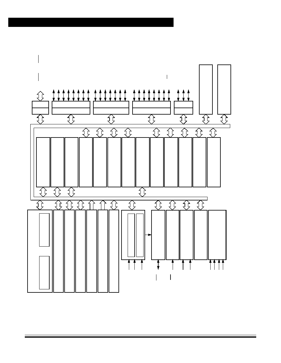
1.3 MCU Block Diagram
Figure 1-1
shows the structure of the MC68HC908GR16.
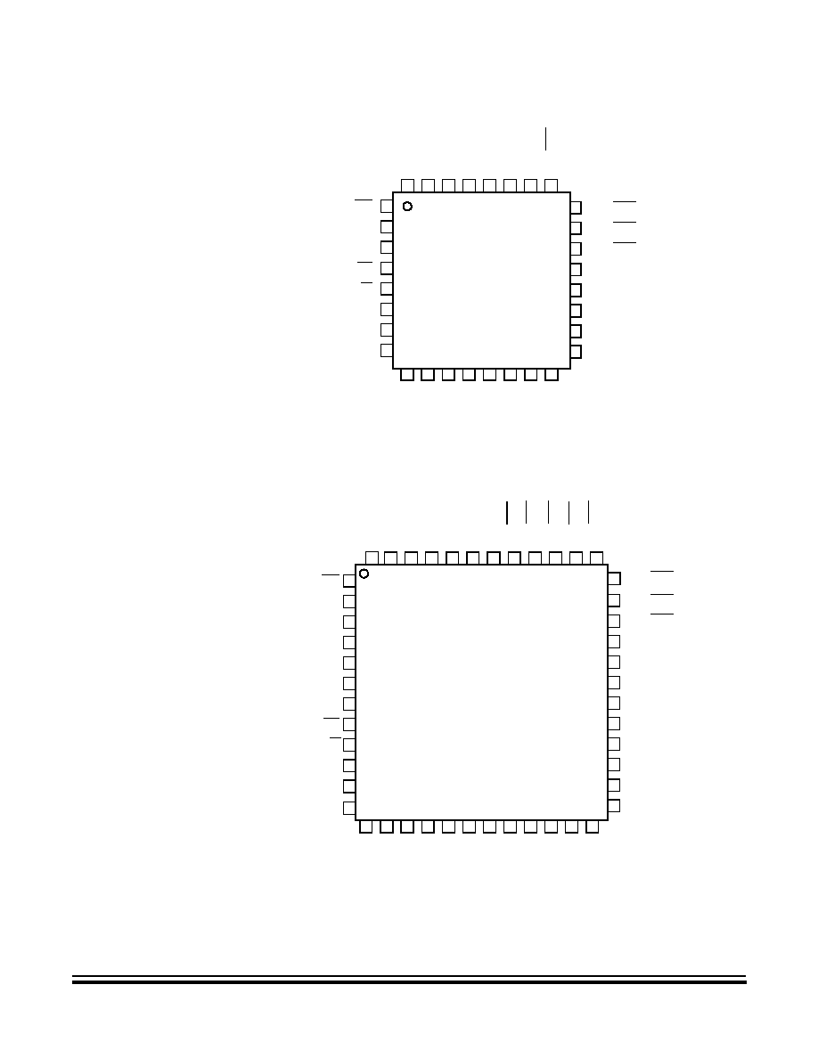
1.4 Pin Assignments
Figure 1-2
and
Figure 1-3
illustrate the pin assignments for the 32-pin LQFP and
48-pin LQFP respectively.
Data Sheet
MC6
8
HC90
8
GR16 --
Re
v. 1.0
22
Gene
ra
l Descriptio
n
MOTOROLA
Gen
e
ral Desc
ription
Figure 1-1. MCU Block Diagram
MONITOR MODULE
M68HC08 CPU
CONTROL AND STATUS REGISTERS -- 64 BYTES
USER FLASH -- 15,872 BYTES
USER RAM -- 1024 BYTES
MONITOR ROM -- 350 BYTES
USER FLASH VECTOR SPACE -- 44 BYTES
PORTA
D
DRA
DDRC
PO
R
T
C
DDR
D
PORTD
DDRE
POR
T
E
INTERNAL BUS
OSC1
OSC2
RST
(3)
IRQ
(3)
PTA7/KBD7�PTA0/KBD0
(1)
PTB7/AD7
PTB6/AD6
PTB5/AD5
PTB4/AD4
PTB3/AD3
PTB2/AD2
PTB1/AD1
PTB0/AD0
PTC6
(1)
PTC5
(1)
PTC4
(1), (2)
PTC3
(1), (2)
PTC2
(1), (2)
PTC1
(1), (2)
PTC0
(1), (2)
PTD7/T2CH1
(1)
PTD6/T2CH0
(1)
PTD5/T1CH1
(1)
PTD4/T1CH0
(1)
PTD3/SPSCK
(1)
PTD2/MOSI
(1)
PTD1/MISO
(1)
PTD0/SS
(1)
PTE1/RxD
PTE0/TxD
SECURITY
MODULE
POWER
V
SS
V
DD
V
SSA
V
DDA
1. Ports are software configurable with pullup device if input port.
2. Higher current drive port pins
3. Pin contains integrated pullup device
MONITOR MODE ENTRY
MODULE
DDRB
PORTB
V
DDAD
/V
REFH
V
DDAD
/V
REFL
PTE5�PTE2
FLASH PROGRAMMING ROUTINES ROM -- 406 BYTES
CLOCK GENERATOR MODULE
CGMXFC
PHASE LOCKED LOOP
32�100 kHz OSCILLATOR
CPU
REGISTERS
ARITHMETIC/LOGIC
UNIT (ALU)
SYSTEM INTEGRATION
MODULE
SINGLE EXTERNAL
INTERRUPT MODULE
10-BIT ANALOG-TO-DIGITAL
CONVERTER MODULE
POWER-ON RESET
MODULE
PROGRAMMABLE TIMEBASE
MODULE
SINGLE BREAKPOINT
BREAK MODULE
DUAL VOLTAGE
LOW-VOLTAGE INHIBIT
MODULE
8-BIT KEYBOARD
INTERRUPT MODULE
2-CHANNEL TIMER
INTERFACE MODULE 1
2-CHANNEL TIMER
INTERFACE MODULE 2
ENHANCED SERIAL
COMUNICATIONS
INTERFACE MODULE
COMPUTER OPERATING
PROPERLY MODULE
SERIAL PERIPHERAL
INTERFACE MODULE
DATA BUS SWITCH
MODULE
MEMORY MAP
MODULE
CONFIGURATION
REGISTER 1�2
MODULE
General Description
Pin Assignments
MC68HC908GR16 -- Rev. 1.0
Data Sheet
MOTOROLA
General Description
23
Figure 1-2. 32-Pin LQFP Pin Assignments
Figure 1-3. 48-Pin LQFP Pin Assignments
PTD3/SPSCK
P
T
A3/KBD3
PTD2/MOSI
PTD1/MISO
PTD0/SS
IRQ
PTE1/RxD
PTE0/TxD
RST
PTA2/KBD2
PTA1/KBD1
PTA0/KBD0
V
SSAD
/V
REFL
V
DDAD
/V
REFH
PTB5/AD5
PTB4/AD4
PTB3/AD3
OSC
1
OSC
2
CG
M
X
F
C
V
SS
A
V
DD
A
PT
C
1
PT
C
0
1
2
3
4
5
6
7
8
9
10
11
12
13
14
15
17
18
19
20
21
22
23
24
25
26
27
28
29
30
31
32
16
PTB2/AD2
V
SS
V
DD
PT
D4/T1CH0
PT
D5/T1CH1
PT
D6/T2CH0
PTB0/AD0
PTB1/AD1
25
36
37
46
45
44
43
42
41
40
39
38
1
2
3
4
5
6
7
8
9
10
14
15
16
17
18
19
20
21
22
13
RST
PTD0/SS
PTD1/MISO
PTD2/MOSI
PTE0/TxD
PTE1/RxD
PTE2
PTE3
PTE4
PTE5
IRQ
PTC
3
PTC
2
PTD7/T2CH
1
PTD6/T2CH
0
PTD5/T1CH
1
P
T
D4/T1CH0
V
DD
V
SS
PTC
4
P
T
B0
/
A
D0
P
T
B1
/
A
D1
PTA
5
/K
BD5
PTA
6
/K
BD6
PTC
1
CGMXF
C
V
SSA
V
DDA
PTA7
/KBD
7
PTC0
PTA4
/KBD
4
PTA
3
/K
BD3
OSC2
11
12
24
23
35
34
33
32
31
30
29
28
27
26
V
DDAD
/V
REFH
V
SSAD
/V
REFL
PTC5
PTC6
PTA0/KBD0
PTB4/AD4
PTB5/AD5
PTB3/AD3
PTB6/AD6
PTB7/AD7
PTA1/KBD1
PTA2/KBD2
P
T
B2
/
A
D2
PTD3/SPSCK
48
OSC
1
47
General Description
Data Sheet
MC68HC908GR16 -- Rev. 1.0
24
General Description
MOTOROLA
1.5 Pin Functions
Descriptions of the pin functions are provided here.
1.5.1 Power Supply Pins (V
DD
and V
SS
)
V
DD
and V
SS
are the power supply and ground pins. The MCU operates from a
single power supply.
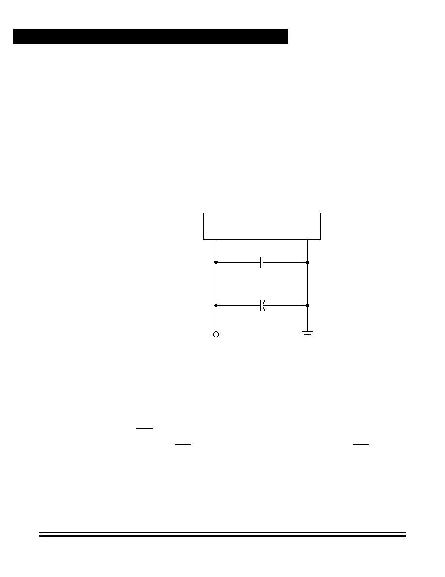
Fast signal transitions on MCU pins place high, short-duration current demands on
the power supply. To prevent noise problems, take special care to provide power
supply bypassing at the MCU as
Figure 1-4
shows. Place the C1 bypass capacitor
as close to the MCU as possible. Use a high-frequency-response ceramic
capacitor for C1. C2 is an optional bulk current bypass capacitor for use in
applications that require the port pins to source high current levels.
Figure 1-4. Power Supply Bypassing
1.5.2 Oscillator Pins (OSC1 and OSC2)
OSC1 and OSC2 are the connections for an external crystal, resonator, or clock
circuit. See
Section 4. Clock Generator Module (CGM)
.
1.5.3 External Reset Pin (RST)
A logic 0 on the RST pin forces the MCU to a known startup state. RST is
bidirectional, allowing a reset of the entire system. It is driven low when any internal
reset source is asserted. This pin contains an internal pullup resistor. See
Section 15. System Integration Module (SIM).
MCU
V
DD
C2
C1
0.1
�F
V
SS
V
DD
+
Note: Component values shown represent typical applications.

General Description
Pin Functions
MC68HC908GR16 -- Rev. 1.0
Data Sheet
MOTOROLA
General Description
25
1.5.4 External Interrupt Pin (IRQ)
IRQ is an asynchronous external interrupt pin. This pin contains an internal pullup
resistor. See
Section 8. External Interrupt (IRQ).
1.5.5 CGM Power Supply Pins (V
DDA
and V
SSA
)
V
DDA
and V
SSA
are the power supply pins for the analog portion of the clock
generator module (CGM). Decoupling of these pins should be as per the digital
supply. See
Section 4. Clock Generator Module (CGM)
.
1.5.6 External Filter Capacitor Pin (V
CGMXFC
)
CGMXFC is an external filter capacitor connection for the CGM. See
Section 4.
Clock Generator Module (CGM)
.
1.5.7 ADC Power Supply/Reference Pins (V
DDAD
/V
REFH
and V
SSAD
/V
REFL
)
V
DDAD
and V
SSAD
are the power supply pins to the analog-to-digital converter
(ADC). V
REFH
and V
REFL
are the reference voltage pins for the ADC. V
REFH
is the
high reference supply for the ADC, and by default the V
DDAD
/V
REFH
pin should be
externally filtered and connected to the same voltage potential as V
DD
. V
REFL
is the
low reference supply for the ADC, and by default the V
SSAD
/V
REFL
pin should be
connected to the same voltage potential as V
SS
. See
Section 3. Analog-to-Digital
Converter (ADC)
.
1.5.8 Port A Input/Output (I/O) Pins (PTA7/KBD7�PTA0/KBD0)
PTA7�PTA0 are general-purpose, bidirectional I/O port pins. Any or all of the port
A pins can be programmed to serve as keyboard interrupt pins. See
Section 12.
Input/Output Ports (PORTS)
and
Section 9. Keyboard Interrupt Module (KBI)
.
These port pins also have selectable pullups when configured for input mode. The
pullups are disengaged when configured for output mode. The pullups are
selectable on an individual port bit basis.
1.5.9 Port B I/O Pins (PTB7/AD7�PTB0/AD0)
PTB7�PTB0 are general-purpose, bidirectional I/O port pins that can also be used
for analog-to-digital converter (ADC) inputs. See
Section 12. Input/Output Ports
(PORTS)
and
Section 3. Analog-to-Digital Converter (ADC)
.
1.5.10 Port C I/O Pins (PTC6�PTC0)
PTC6 and PTC5 are general-purpose, bidirectional I/O port pins. PTC4�PTC0 are
general-purpose, bidirectional I/O port pins that contain higher current sink/source
capability. See
Section 12. Input/Output Ports (PORTS)
.

General Description
Data Sheet
MC68HC908GR16 -- Rev. 1.0
26
General Description
MOTOROLA
These port pins also have selectable pullups when configured for input mode. The
pullups are disengaged when configured for output mode. The pullups are
selectable on an individual port bit basis.
1.5.11 Port D I/O Pins (PTD7/T2CH1�PTD0/SS)
PTD7�PTD0 are special-function, bidirectional I/O port pins. PTD3�PTD0 can be
programmed to be serial peripheral interface (SPI) pins, while PTD7�PTD4 can be
individually programmed to be timer interface module (TIM1 and TIM2) pins. See
Section 18. Timer Interface Module (TIM)
,
Section 16. Serial Peripheral
Interface (SPI) Module
, and
Section 12. Input/Output Ports (PORTS)
.
These port pins also have selectable pullups when configured for input mode. The
pullups are disengaged when configured for output mode. The pullups are
selectable on an individual port bit basis.
1.5.12 Port E I/O Pins (PTE5�PTE2, PTE1/RxD, and PTE0/TxD)
PTE5�PTE0 are general-purpose, bidirectional I/O port pins. PTE1 and PTE0 can
also be programmed to be enhanced serial communications interface (ESCI) pins.
See
Section 14. Enhanced Serial Communications Interface (ESCI) Module
and
Section 12. Input/Output Ports (PORTS)
.
NOTE:
Any unused inputs and I/O ports should be tied to an appropriate logic level (either
V
DD
or V
SS
). Although the I/O ports of the MC68HC908GR16 do not require
termination, termination is recommended to reduce the possibility of static damage.

MC68HC908GR16 -- Rev. 1.0
Data Sheet
MOTOROLA
Memory
27
Data Sheet -- MC68HC908GR16
Section 2. Memory
2.1 Introduction
The CPU08 can address 64 Kbytes of memory space. The memory map, shown in
Figure 2-1
, includes:
�
15,872 bytes of user FLASH memory
�
1024 bytes of random-access memory (RAM)
�
406 bytes of FLASH programming routines read-only memory (ROM)
�
44 bytes of user-defined vectors
�
350 bytes of monitor ROM
2.2 Unimplemented Memory Locations
Accessing an unimplemented location can cause an illegal address reset. In the
memory map (
Figure 2-1
) and in register figures in this document, unimplemented
locations are shaded.
2.3 Reserved Memory Locations
Accessing a reserved location can have unpredictable effects on microcontroller
(MCU) operation. In the
Figure 2-1
and in register figures in this document,
reserved locations are marked with the word Reserved or with the letter R.
2.4 Input/Output (I/O) Section
Most of the control, status, and data registers are in the zero page area of
$0000�$003F. Additional I/O registers have these addresses:
�
$FE00; break status register, BSR
�
$FE01; SIM reset status register, SRSR
�
$FE02; break auxiliary register, BRKAR
�
$FE03; break flag control register, BFCR
�
$FE04; interrupt status register 1, INT1
�
$FE05; interrupt status register 2, INT2
�
$FE06; interrupt status register 3, INT3
�
$FE07; reserved

Memory
Data Sheet
MC68HC908GR16 -- Rev. 1.0
28
Memory
MOTOROLA
�
$FE08; FLASH control register, FLCR
�
$FE09; break address register high, BRKH
�
$FE0A; break address register low, BRKL
�
$FE0B; break status and control register, BRKSCR
�
$FE0C; LVI status register, LVISR
�
$FF7E; FLASH block protect register, FLBPR
Data registers are shown in
Figure 2-2
.
Table 2-1
is a list of vector locations.
$0000
I/O REGISTERS
64 BYTES
$003F
$0040
RAM
1024 BYTES
$043F
$0440
$04FF
UNIMPLEMENTED
192 BYTES
$0500
$057F
RESERVED
128 BYTES
$0580
$1BFF
UNIMPLEMENTED
5760 BYTES
$1C00
FLASH PROGRAMMING ROUTINES ROM
406 BYTES
$1D95
$1D96
UNIMPLEMENTED
41,578 BYTES
$BFFF
$C000
FLASH MEMORY
15,872 BYTES
$FDFF
$FE00
BREAK STATUS REGISTER (BSR)
$FE01
SIM RESET STATUS REGISTER (SRSR)
Figure 2-1. Memory Map
Memory
Input/Output (I/O) Section
MC68HC908GR16 -- Rev. 1.0
Data Sheet
MOTOROLA
Memory
29
$FE02
BREAK AUXILIARY REGISTER (BRKAR)
$FE03
BREAK FLAG CONTROL REGISTER (BFCR)
$FE04
INTERRUPT STATUS REGISTER 1 (INT1)
$FE05
INTERRUPT STATUS REGISTER 2 (INT2)
$FE06
INTERRUPT STATUS REGISTER 3 (INT3)
$FE07
RESERVED
$FE08
FLASH CONTROL REGISTER (FLCR)
$FE09
BREAK ADDRESS REGISTER HIGH (BRKH)
$FE0A
BREAK ADDRESS REGISTER LOW (BRKL)
$FE0B
BREAK STATUS AND CONTROL REGISTER (BRKSCR)
$FE0C
LVI STATUS REGISTER (LVISR)
$FE0D
UNIMPLEMENTED
3 BYTES
$FE0F
$FE10
UNIMPLEMENTED
16 BYTES
RESERVED FOR COMPATIBILITY WITH MONITOR CODE
FOR A-FAMILY PART
$FE1F
$FE20
MONITOR ROM
350 BYTES
$FF7D
$FF7E
FLASH BLOCK PROTECT REGISTER (FLBPR)
$FF7F
UNIMPLEMENTED
85 BYTES
$FFD3
$FFD4
FLASH VECTORS
44 BYTES
$FFFF
(1)
1. $FFF6�$FFFD used for eight security bytes
Figure 2-1. Memory Map (Continued)
Memory
Data Sheet
MC68HC908GR16 -- Rev. 1.0
30
Memory
MOTOROLA
Addr.
Register Name
Bit 7
6
5
4
3
2
1
Bit 0
$0000
Port A Data Register
(PTA)
See page 132.
Read:
PTA7
PTA6
PTA5
PTA4
PTA3
PTA2
PTA1
PTA0
Write:
Reset:
Unaffected by reset
$0001
Port B Data Register
(PTB)
See page 134.
Read:
PTB7
PTB6
PTB5
PTB4
PTB3
PTB2
PTB1
PTB0
Write:
Reset:
Unaffected by reset
$0002
Port C Data Register
(PTC)
See page 136.
Read:
0
PTC6
PTC5
PTC4
PTC3
PTC2
PTC1
PTC0
Write:
Reset:
Unaffected by reset
$0003
Port D Data Register
(PTD)
See page 138.
Read:
PTD7
PTD6
PTD5
PTD4
PTD3
PTD2
PTD1
PTD0
Write:
Reset:
Unaffected by reset
$0004
Data Direction Register A
(DDRA)
See page 132.
Read:
DDRA7
DDRA6
DDRA5
DDRA4
DDRA3
DDRA2
DDRA1
DDRA0
Write:
Reset:
0
0
0
0
0
0
0
0
$0005
Data Direction Register B
(DDRB)
See page 135.
Read:
DDRB7
DDRB6
DDRB5
DDRB4
DDRB3
DDRB2
DDRB1
DDRB0
Write:
Reset:
0
0
0
0
0
0
0
0
$0006
Data Direction Register C
(DDRC)
See page 136.
Read:
0
DDRC6
DDRC5
DDRC4
DDRC3
DDRC2
DDRC1
DDRC0
Write:
Reset:
0
0
0
0
0
0
0
0
$0007
Data Direction Register D
(DDRD)
See page 139.
Read:
DDRD7
DDRD6
DDRD5
DDRD4
DDRD3
DDRD2
DDRD1
DDRD0
Write:
Reset:
0
0
0
0
0
0
0
0
$0008
Port E Data Register
(PTE)
See page 141.
Read:
0
0
PTE5
PTE4
PTE3
PTE2
PTE1
PTE0
Write:
Reset:
Unaffected by reset
$0009
ESCI Prescaler Register
(SCPSC)
See page 187.
Read:
PS2
PS1
PS0
PSSB4
PSSB3
PSSB2
PSSB1
PSSB0
Write:
Reset:
0
0
0
0
0
0
0
0
$000A
ESCI Arbiter Control Register
(SCIACTL)
See page 191.
Read:
AM1
ALOST
AM0
ACLK
AFIN
ARUN
AOVFL
ARD8
Write:
Reset:
0
0
0
0
0
0
0
0
$000B
ESCI Arbiter Data
Register (SCIADAT)
See page 192.
Read:
ARD7
ARD6
ARD5
ARD4
ARD3
ARD2
ARD1
ARD0
Write:
Reset:
0
0
0
0
0
0
0
0
= Unimplemented
R
= Reserved
U = Unaffected
Figure 2-2. Control, Status, and Data Registers (Sheet 1 of 7)
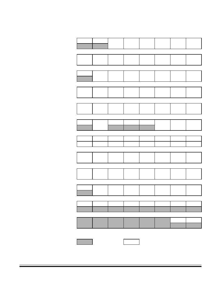
Memory
Input/Output (I/O) Section
MC68HC908GR16 -- Rev. 1.0
Data Sheet
MOTOROLA
Memory
31
$000C
Data Direction Register E
(DDRE)
See page 142.
Read:
0
0
DDRE5
DDRE4
DDRE3
DDRE2
DDRE1
DDRE0
Write:
Reset:
0
0
0
0
0
0
0
0
$000D
Port A Input Pullup Enable
Register (PTAPUE)
See page 134.
Read:
PTAPUE7
PTAPUE6
PTAPUE5
PTAPUE4
PTAPUE3
PTAPUE2
PTAPUE1
PTAPUE0
Write:
Reset:
0
0
0
0
0
0
0
0
$000E
Port C Input Pullup Enable
Register (PTCPUE)
See page 138.
Read:
0
PTCPUE6
PTCPUE5
PTCPUE4
PTCPUE3
PTCPUE2
PTCPUE1
PTCPUE0
Write:
Reset:
0
0
0
0
0
0
0
0
$000F
Port D Input Pullup Enable
Register (PTDPUE)
See page 141.
Read:
PTDPUE7
PTDPUE6
PTDPUE5
PTDPUE4
PTDPUE3
PTDPUE2
PTDPUE1
PTDPUE0
Write:
Reset:
0
0
0
0
0
0
0
0
$0010
SPI Control Register
(SPCR)
See page 235.
Read:
SPRIE
R
SPMSTR
CPOL
CPHA
SPWOM
SPE
SPTIE
Write:
Reset:
0
0
1
0
1
0
0
0
$0011
SPI Status and Control
Register (SPSCR)
See page 236.
Read:
SPRF
ERRIE
OVRF
MODF
SPTE
MODFEN
SPR1
SPR0
Write:
Reset:
0
0
0
0
1
0
0
0
$0012
SPI Data Register
(SPDR)
See page 238.
Read:
R7
R6
R5
R4
R3
R2
R1
R0
Write:
T7
T6
T5
T4
T3
T2
T1
T0
Reset:
Unaffected by reset
$0013
ESCI Control Register 1
(SCC1)
See page 176.
Read:
LOOPS
ENSCI
TXINV
M
WAKE
ILTY
PEN
PTY
Write:
Reset:
0
0
0
0
0
0
0
0
$0014
ESCI Control Register 2
(SCC2)
See page 178.
Read:
SCTIE
TCIE
SCRIE
ILIE
TE
RE
RWU
SBK
Write:
Reset:
0
0
0
0
0
0
0
0
$0015
ESCI Control Register 3
(SCC3)
See page 180.
Read:
R8
T8
R
R
ORIE
NEIE
FEIE
PEIE
Write:
Reset:
U
0
0
0
0
0
0
0
$0016
ESCI Status Register 1
(SCS1)
See page 181.
Read:
SCTE
TC
SCRF
IDLE
OR
NF
FE
PE
Write:
Reset:
1
1
0
0
0
0
0
0
$0017
ESCI Status Register 2
(SCS2)
See page 184.
Read:
BKF
RPF
Write:
Reset:
0
0
0
0
0
0
0
0
Addr.
Register Name
Bit 7
6
5
4
3
2
1
Bit 0
= Unimplemented
R
= Reserved
U = Unaffected
Figure 2-2. Control, Status, and Data Registers (Sheet 2 of 7)
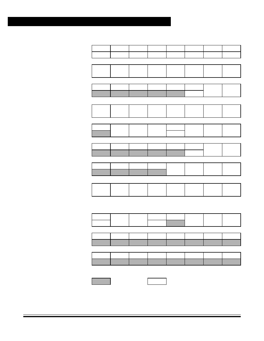
Memory
Data Sheet
MC68HC908GR16 -- Rev. 1.0
32
Memory
MOTOROLA
$0018
ESCI Data Register
(SCDR)
See page 185.
Read:
R7
R6
R5
R4
R3
R2
R1
R0
Write:
T7
T6
T5
T4
T3
T2
T1
T0
Reset:
Unaffected by reset
$0019
ESCI Baud Rate Register
(SCBR)
See page 185.
Read:
LINT
LINR
SCP1
SCP0
R
SCR2
SCR1
SCR0
Write:
Reset:
0
0
0
0
0
0
0
0
$001A
Keyboard Status
and Control Register
(INTKBSCR)
See page 114.
Read:
0
0
0
0
KEYF
0
IMASKK
MODEK
Write:
ACKK
Reset:
0
0
0
0
0
0
0
0
$001B
Keyboard Interrupt Enable
Register (INTKBIER)
See page 115.
Read:
KBIE7
KBIE6
KBIE5
KBIE4
KBIE3
KBIE2
KBIE1
KBIE0
Write:
Reset:
0
0
0
0
0
0
0
0
$001C
Timebase Module Control
Register (TBCR)
See page 242.
Read:
TBIF
TBR2
TBR1
TBR0
0
TBIE
TBON
R
Write:
TACK
Reset:
0
0
0
0
0
0
0
0
$001D
IRQ Status and Control
Register (INTSCR)
See page 107.
Read:
0
0
0
0
IRQF
0
IMASK
MODE
Write:
ACK
Reset:
0
0
0
0
0
0
0
0
$001E
Configuration Register 2
(CONFIG2)
(1)
See page 82.
Read:
0
0
0
0
R
TMCLKSEL
OSCENIN-
STOP
SCIBDSRC
Write:
Reset:
0
0
0
0
0
0
0
1
$001F
Configuration Register 1
(CONFIG1)
(1)
See page 82.
Read:
COPRS
LVISTOP
LVIRSTD
LVIPWRD
LVI5OR3
(Note 1)
SSREC
STOP
COPD
Write:
Reset:
0
0
0
0
0
0
0
0
1.
One-time writable register after each reset, except LVI5OR3 bit. LVI5OR3 bit is only reset via POR (power-on reset).
$0020
Timer 1 Status and Control
Register (T1SC)
See page 256.
Read:
TOF
TOIE
TSTOP
0
0
PS2
PS1
PS0
Write:
0
TRST
Reset:
0
0
1
0
0
0
0
0
$0021
Timer 1 Counter
Register High (T1CNTH)
See page 258.
Read:
Bit 15
14
13
12
11
10
9
Bit 8
Write:
Reset:
0
0
0
0
0
0
0
0
$0022
Timer 1 Counter
Register Low (T1CNTL)
See page 258.
Read:
Bit 7
6
5
4
3
2
1
Bit 0
Write:
Reset:
0
0
0
0
0
0
0
0
Addr.
Register Name
Bit 7
6
5
4
3
2
1
Bit 0
= Unimplemented
R
= Reserved
U = Unaffected
Figure 2-2. Control, Status, and Data Registers (Sheet 3 of 7)
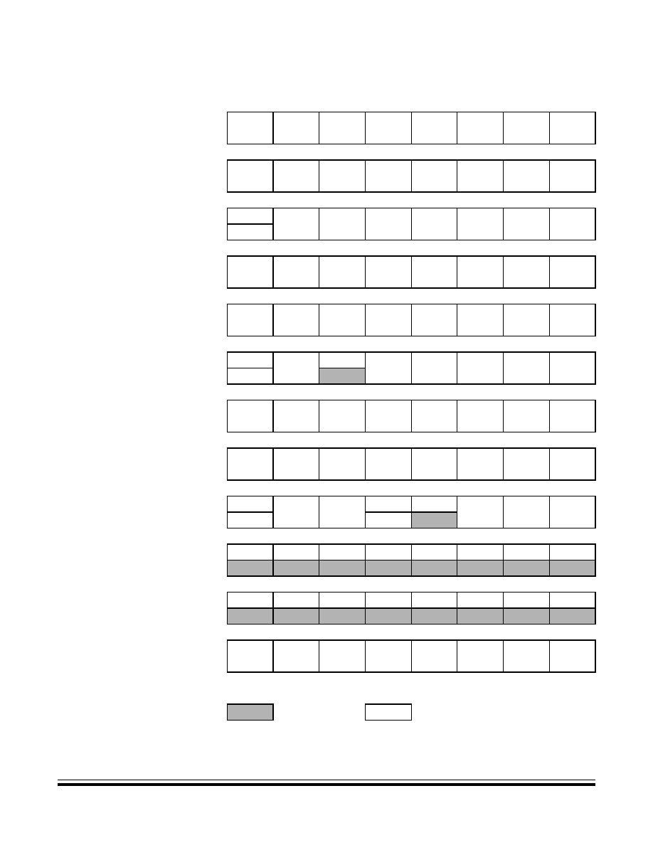
Memory
Input/Output (I/O) Section
MC68HC908GR16 -- Rev. 1.0
Data Sheet
MOTOROLA
Memory
33
$0023
Timer 1 Counter Modulo
Register High (T1MODH)
See page 258.
Read:
Bit 15
14
13
12
11
10
9
Bit 8
Write:
Reset:
1
1
1
1
1
1
1
1
$0024
Timer 1 Counter Modulo
Register Low (T1MODL)
See page 259.
Read:
Bit 7
6
5
4
3
2
1
Bit 0
Write:
Reset:
1
1
1
1
1
1
1
1
$0025
Timer 1 Channel 0 Status and
Control Register (T1SC0)
See page 259.
Read:
CH0F
CH0IE
MS0B
MS0A
ELS0B
ELS0A
TOV0
CH0MAX
Write:
0
Reset:
0
0
0
0
0
0
0
0
$0026
Timer 1 Channel 0
Register High (T1CH0H)
See page 262.
Read:
Bit 15
14
13
12
11
10
9
Bit 8
Write:
Reset:
Indeterminate after reset
$0027
Timer 1 Channel 0
Register Low (T1CH0L)
See page 262.
Read:
Bit 7
6
5
4
3
2
1
Bit 0
Write:
Reset:
Indeterminate after reset
$0028
Timer 1 Channel 1 Status and
Control Register (T1SC1)
See page 259.
Read:
CH1F
CH1IE
0
MS1A
ELS1B
ELS1A
TOV1
CH1MAX
Write:
0
Reset:
0
0
0
0
0
0
0
0
$0029
Timer 1 Channel 1
Register High (T1CH1H)
See page 262.
Read:
Bit 15
14
13
12
11
10
9
Bit 8
Write:
Reset:
Indeterminate after reset
$002A
Timer 1 Channel 1
Register Low (T1CH1L)
See page 262.
Read:
Bit 7
6
5
4
3
2
1
Bit 0
Write:
Reset:
Indeterminate after reset
$002B
Timer 2 Status and Control
Register (T2SC)
See page 256.
Read:
TOF
TOIE
TSTOP
0
0
PS2
PS1
PS0
Write:
0
TRST
Reset:
0
0
1
0
0
0
0
0
$002C
Timer 2 Counter
Register High (T2CNTH)
See page 258.
Read:
Bit 15
14
13
12
11
10
9
Bit 8
Write:
Reset:
0
0
0
0
0
0
0
0
$002D
Timer 2 Counter
Register Low (T2CNTL)
See page 258.
Read:
Bit 7
6
5
4
3
2
1
Bit 0
Write:
Reset:
0
0
0
0
0
0
0
0
$002E
Timer 2 Counter Modulo
Register High (T2MODH)
See page 258.
Read:
Bit 15
14
13
12
11
10
9
Bit 8
Write:
Reset:
1
1
1
1
1
1
1
1
Addr.
Register Name
Bit 7
6
5
4
3
2
1
Bit 0
= Unimplemented
R
= Reserved
U = Unaffected
Figure 2-2. Control, Status, and Data Registers (Sheet 4 of 7)
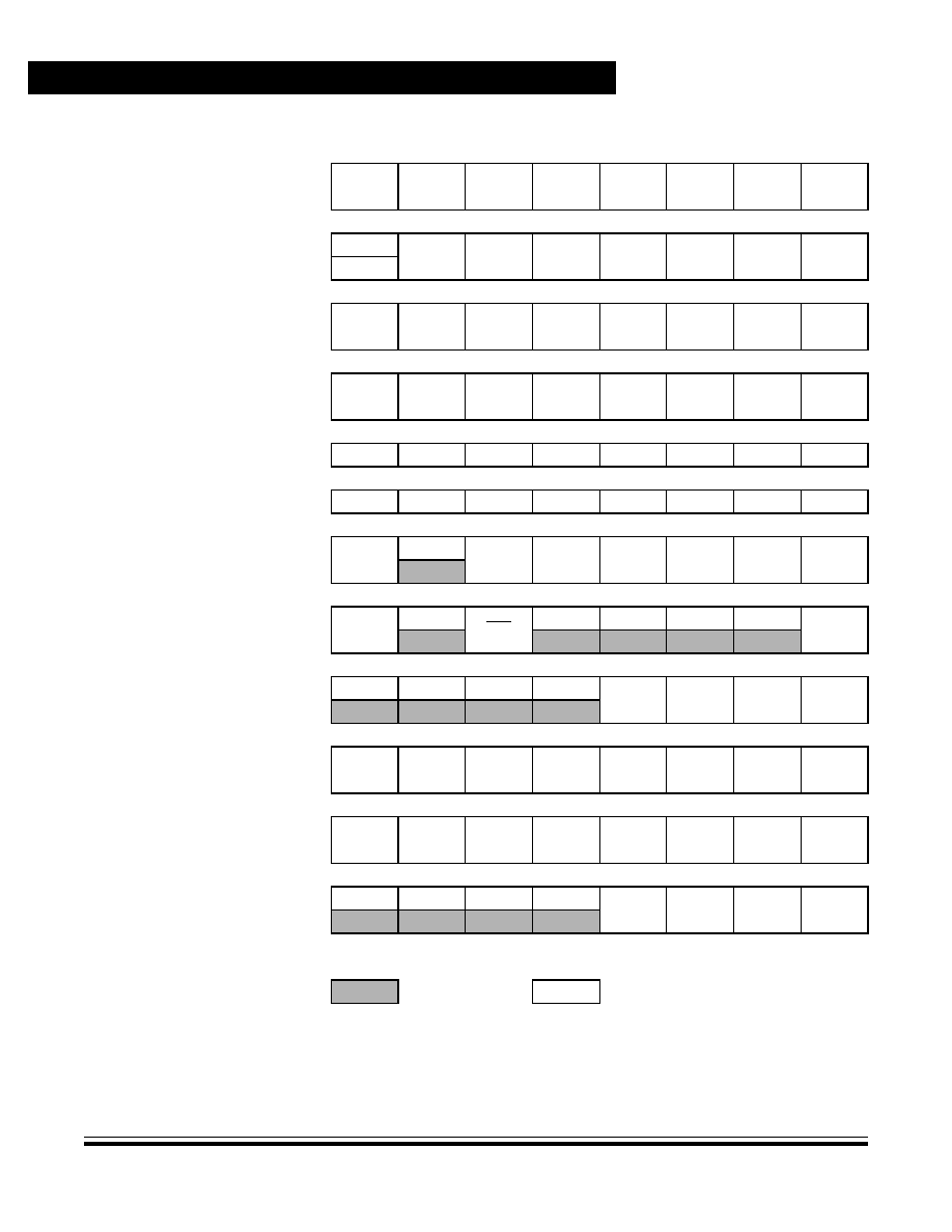
Memory
Data Sheet
MC68HC908GR16 -- Rev. 1.0
34
Memory
MOTOROLA
$002F
Timer 2 Counter Modulo
Register Low (T2MODL)
See page 259.
Read:
Bit 7
6
5
4
3
2
1
Bit 0
Write:
Reset:
1
1
1
1
1
1
1
1
$0030
Timer 2 Channel 0 Status and
Control Register (T2SC0)
See page 259.
Read:
CH0F
CH0IE
MS0B
MS0A
ELS0B
ELS0A
TOV0
CH0MAX
Write:
0
Reset:
0
0
0
0
0
0
0
0
$0031
Timer 2 Channel 0
Register High (T2CH0H)
See page 262.
Read:
Bit 15
14
13
12
11
10
9
Bit 8
Write:
Reset:
Indeterminate after reset
$0032
Timer 2 Channel 0
Register Low (T2CH0L)
See page 262.
Read:
Bit 7
6
5
4
3
2
1
Bit 0
Write:
Reset:
Indeterminate after reset
$0033
Reserved
R
R
R
R
R
R
R
R
$0035
Reserved
R
R
R
R
R
R
R
R
$0036
PLL Control Register
(PCTL)
See page 71.
Read:
PLLIE
PLLF
PLLON
BCS
PRE1
PRE0
VPR1
VPR0
Write:
Reset:
0
0
1
0
0
0
0
0
$0037
PLL Bandwidth Control
Register (PBWC)
See page 73.
Read:
AUTO
LOCK
ACQ
0
0
0
0
R
Write:
Reset:
0
0
0
0
0
0
0
0
$0038
PLL Multiplier Select High
Register (PMSH)
See page 74.
Read:
0
0
0
0
MUL11
MUL10
MUL9
MUL8
Write:
Reset:
0
0
0
0
0
0
0
0
$0039
PLL Multiplier Select Low
Register (PMSL)
See page 75.
Read:
MUL7
MUL6
MUL5
MUL4
MUL3
MUL2
MUL1
MUL0
Write:
Reset:
0
1
0
0
0
0
0
0
$003A
PLL VCO Select Range
Register (PMRS)
See page 75.
Read:
VRS7
VRS6
VRS5
VRS4
VRS3
VRS2
VRS1
VRS0
Write:
Reset:
0
1
0
0
0
0
0
0
$003B
PLL Reference Divider
Select Register (PMDS)
See page 76.
Read:
0
0
0
0
RDS3
RDS2
RDS1
RDS0
Write:
Reset:
0
0
0
0
0
0
0
1
Addr.
Register Name
Bit 7
6
5
4
3
2
1
Bit 0
= Unimplemented
R
= Reserved
U = Unaffected
Figure 2-2. Control, Status, and Data Registers (Sheet 5 of 7)
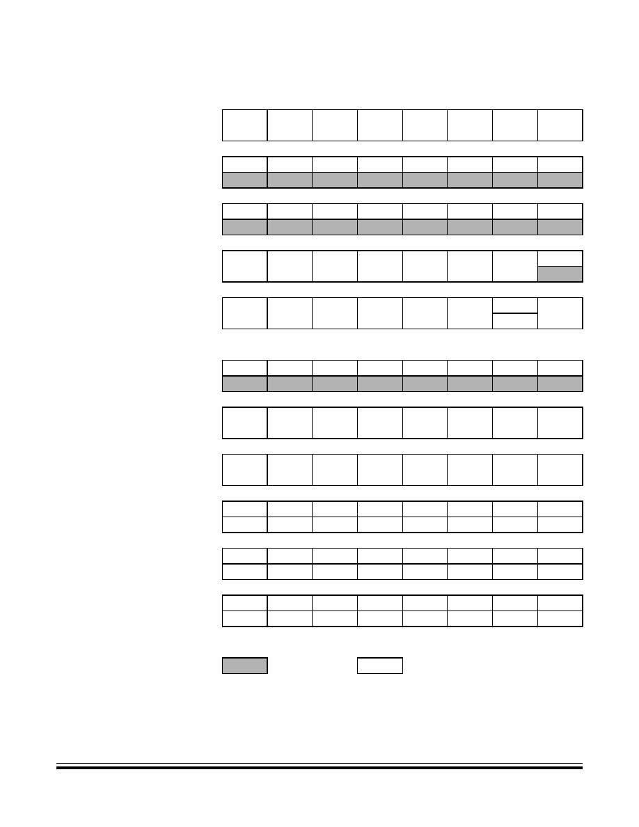
Memory
Input/Output (I/O) Section
MC68HC908GR16 -- Rev. 1.0
Data Sheet
MOTOROLA
Memory
35
$003C
ADC Status and Control
Register (ADSCR)
See page 54.
Read:
COCO
AIEN
ADCO
ADCH4
ADCH3
ADCH2
ADCH1
ADCH0
Write:
Reset:
0
0
0
1
1
1
1
1
$003D
ADC Data High Register
(ADRH)
See page 55.
Read:
0
0
0
0
0
0
AD9
AD9
Write:
Reset:
Unaffected by reset
$003E
ADC Data Low Register
(ADRL)
See page 55.
Read:
AD7
AD6
AD5
AD4
A3
AD2
AD1
AD0
Write:
Reset:
Unaffected by reset
$003F
ADC Clock Register
(ADCLK)
See page 57.
Read:
ADIV2
ADIV1
ADIV0
ADICLK
MODE1
MODE0
R
0
Write:
Reset:
0
0
0
0
0
1
0
0
$FE00
Break Status Register
(BSR)
See page 267.
Read:
R
R
R
R
R
R
SBSW
R
Write:
(Note 2)
Reset:
0
0
0
0
0
0
0
0
2. Writing a logic 0 clears SBSW.
$FE01
SIM Reset Status Register
(SRSR)
See page 213.
Read:
POR
PIN
COP
ILOP
ILAD
MODRST
LVI
0
Write:
POR:
1
0
0
0
0
0
0
0
$FE02
Break Auxiliary Register
(BRKAR)
See page 267.
Read:
Bit 7
6
5
4
3
2
1
Bit 0
Write:
Reset:
0
0
0
0
0
0
0
0
$FE03
Break Flag Control
Register (BFCR)
See page 268.
Read:
BCFE
R
R
R
R
R
R
R
Write:
Reset:
0
0
0
0
0
0
0
0
$FE04
Interrupt Status Register 1
(INT1)
See page 156.
Read:
IF6
IF5
IF4
IF3
IF2
IF1
0
0
Write:
R
R
R
R
R
R
R
R
Reset:
0
0
0
0
0
0
0
0
$FE05
Interrupt Status Register 2
(INT2)
See page 157.
Read:
IF14
IF13
IF12
IF11
IF10
IF9
IF8
IF7
Write:
R
R
R
R
R
R
R
R
Reset:
0
0
0
0
0
0
0
0
$FE06
Interrupt Status Register 3
(INT3)
See page 157.
Read:
0
0
IF20
IF19
IF18
IF17
IF16
IF15
Write:
R
R
R
R
R
R
R
R
Reset:
0
0
0
0
0
0
0
0
Addr.
Register Name
Bit 7
6
5
4
3
2
1
Bit 0
= Unimplemented
R
= Reserved
U = Unaffected
Figure 2-2. Control, Status, and Data Registers (Sheet 6 of 7)
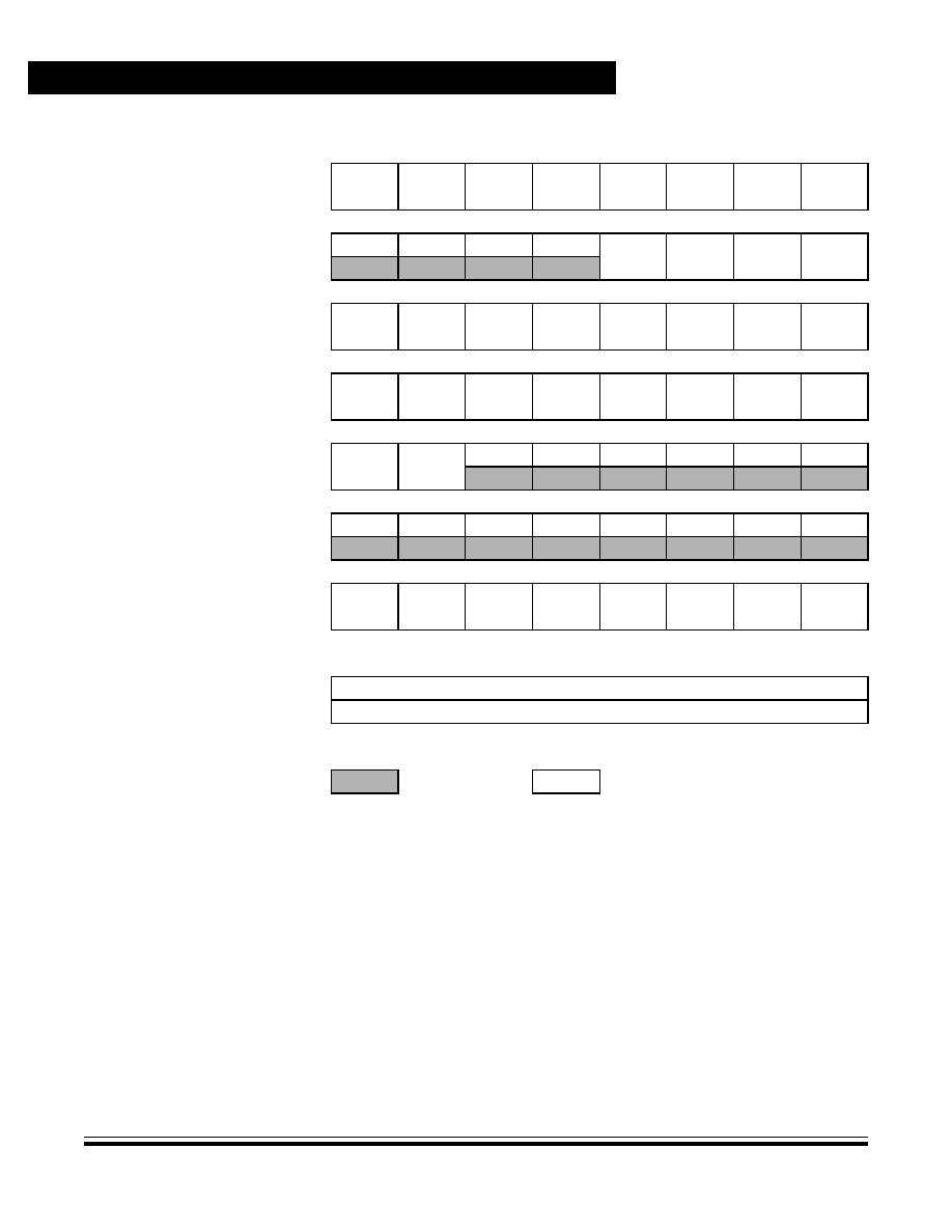
Memory
Data Sheet
MC68HC908GR16 -- Rev. 1.0
36
Memory
MOTOROLA
$FE07
Reserved
Read:
R
R
R
R
R
R
R
R
Write:
Reset:
0
0
0
0
0
0
0
0
$FE08
FLASH Control Register
(FLCR)
See page 39.
Read:
0
0
0
0
HVEN
MASS
ERASE
PGM
Write:
Reset:
0
0
0
0
0
0
0
0
$FE09
Break Address Register High
(BRKH)
See page 266.
Read:
Bit 15
14
13
12
11
10
9
Bit 8
Write:
Reset:
0
0
0
0
0
0
0
0
$FE0A
Break Address Register Low
(BRKL)
See page 266.
Read:
Bit 7
6
5
4
3
2
1
Bit 0
Write:
Reset:
0
0
0
0
0
0
0
0
$FE0B
Break Status and Control
Register (BRKSCR)
See page 266.
Read:
BRKE
BRKA
0
0
0
0
0
0
Write:
Reset:
0
0
0
0
0
0
0
0
$FE0C
LVI Status Register (LVISR)
See page 127.
Read:
LVIOUT
0
0
0
0
0
0
0
Write:
Reset:
0
0
0
0
0
0
0
0
$FF7E
FLASH Block Protect
Register (FLBPR)
(3)
See page 44.
Read:
BPR7
BPR6
BPR5
BPR4
BPR3
BPR2
BPR1
BPR0
Write:
Reset:
Unaffected by reset
3. Non-volatile FLASH register
$FFFF
COP Control Register
(COPCTL)
See page 87.
Read:
Low byte of reset vector
Write:
Writing clears COP counter (any value)
Reset:
Unaffected by reset
Addr.
Register Name
Bit 7
6
5
4
3
2
1
Bit 0
= Unimplemented
R
= Reserved
U = Unaffected
Figure 2-2. Control, Status, and Data Registers (Sheet 7 of 7)
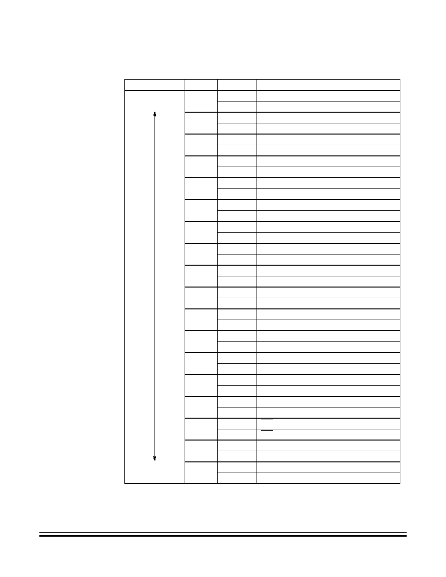
Memory
Input/Output (I/O) Section
MC68HC908GR16 -- Rev. 1.0
Data Sheet
MOTOROLA
Memory
37
Table 2-1. Vector Addresses
Vector Priority
Vector
Address
Vector
Lowest
IF16
$FFDC
Timebase Vector (High)
$FFDD
Timebase Vector (Low)
IF15
$FFDE
ADC Conversion Complete Vector (High)
$FFDF
ADC Conversion Complete Vector (Low)
IF14
$FFE0
Keyboard Vector (High)
$FFE1
Keyboard Vector (Low)
IF13
$FFE2
ESCI Transmit Vector (High)
$FFE3
ESCI Transmit Vector (Low)
IF12
$FFE4
ESCI Receive Vector (High)
$FFE5
ESCI Receive Vector (Low)
IF11
$FFE6
ESCI Error Vector (High)
$FFE7
ESCI Error Vector (Low)
IF10
$FFE8
SPI Transmit Vector (High)
$FFE9
SPI Transmit Vector (Low)
IF9
$FFEA
SPI Receive Vector (High)
$FFEB
SPI Receive Vector (Low)
IF8
$FFEC
TIM2 Overflow Vector (High)
$FFED
TIM2 Overflow Vector (Low)
IF7
$FFEE
Reserved
$FFEF
Reserved
IF6
$FFF0
TIM2 Channel 0 Vector (High)
$FFF1
TIM2 Channel 0 Vector (Low)
IF5
$FFF2
TIM1 Overflow Vector (High)
$FFF3
TIM1 Overflow Vector (Low)
IF4
$FFF4
TIM1 Channel 1 Vector (High)
$FFF5
TIM1 Channel 1 Vector (Low)
IF3
$FFF6
TIM1 Channel 0 Vector (High)
$FFF7
TIM1 Channel 0 Vector (Low)
IF2
$FFF8
PLL Vector (High)
$FFF9
PLL Vector (Low)
IF1
$FFFA
IRQ Vector (High)
$FFFB
IRQ Vector (Low)
--
$FFFC
SWI Vector (High)
$FFFD
SWI Vector (Low)
--
$FFFE
Reset Vector (High)
Highest
$FFFF
Reset Vector (Low)

Memory
Data Sheet
MC68HC908GR16 -- Rev. 1.0
38
Memory
MOTOROLA
2.5 Random-Access Memory (RAM)
Addresses $0040 through $043F are RAM locations. The location of the stack
RAM is programmable. The 16-bit stack pointer allows the stack to be anywhere in
the 64-Kbyte memory space.
NOTE:
For correct operation, the stack pointer must point only to RAM locations.
Within page zero are 192 bytes of RAM. Because the location of the stack RAM is
programmable, all page zero RAM locations can be used for I/O control and user
data or code. When the stack pointer is moved from its reset location at $00FF out
of page zero, direct addressing mode instructions can efficiently access all page
zero RAM locations. Page zero RAM, therefore, provides ideal locations for
frequently accessed global variables.
Before processing an interrupt, the CPU uses five bytes of the stack to save the
contents of the CPU registers.
NOTE:
For M6805 compatibility, the H register is not stacked.
During a subroutine call, the CPU uses two bytes of the stack to store the return
address. The stack pointer decrements during pushes and increments during pulls.
NOTE:
Be careful when using nested subroutines. The CPU may overwrite data in the
RAM during a subroutine or during the interrupt stacking operation.
2.6 FLASH Memory (FLASH)
This subsection describes the operation of the embedded FLASH memory. This
memory can be read, programmed, and erased from a single external supply. The
program, erase, and read operations are enabled through the use of an internal
charge pump. It is recommended that the user utilize the FLASH programming
routines provided in the on-chip ROM, which are described more fully in a separate
Motorola application note.
2.6.1 Functional Description
The FLASH memory is an array of 15,872 bytes with an additional 44 bytes of user
vectors and one byte of block protection. An erased bit reads as logic 1 and a
programmed bit reads as a logic 0. Memory in the FLASH array is organized into
two rows per page basis. For the 16-K word by 8-bit embedded FLASH memory,
the page size is 64 bytes per page and the row size is 32 bytes per row. Hence the
minimum erase page size is 64 bytes and the minimum program row size is 32
bytes. Program and erase operation operations are facilitated through control bits
in FLASH control register (FLCR). Details for these operations appear later in this
section.

Memory
FLASH Memory (FLASH)
MC68HC908GR16 -- Rev. 1.0
Data Sheet
MOTOROLA
Memory
39
The address ranges for the user memory and vectors are:
�
$C000�$FDFF; user memory
�
$FE08
;
FLASH control register
�
$FF7E; FLASH block protect register
�
$FFD4�$FFFF; these locations are reserved for user-defined interrupt and
reset vectors
Programming tools are available from Motorola. Contact your local Motorola
representative for more information.
NOTE:
A security feature prevents viewing of the FLASH contents.
(1)
2.6.1.1 FLASH Control Register
The FLASH control register (FLCR) controls FLASH program and erase
operations.
HVEN -- High-Voltage Enable Bit
This read/write bit enables the charge pump to drive high voltages for program
and erase operations in the array. HVEN can only be set if either PGM = 1 or
ERASE = 1 and the proper sequence for program or erase is followed.
1 = High voltage enabled to array and charge pump on
0 = High voltage disabled to array and charge pump off
MASS -- Mass Erase Control Bit
Setting this read/write bit configures the 16-Kbyte FLASH array for mass erase
operation.
1 = MASS erase operation selected
0 = PAGE erase operation selected
ERASE -- Erase Control Bit
This read/write bit configures the memory for erase operation. ERASE is
interlocked with the PGM bit such that both bits cannot be equal to 1 or set to 1
at the same time.
1 = Erase operation selected
0 = Erase operation unselected
1. No security feature is absolutely secure. However, Motorola's strategy is to make reading or copy-
ing the FLASH difficult for unauthorized users.
Address:
$FE08
Bit 7
6
5
4
3
2
1
Bit 0
Read:
0
0
0
0
HVEN
MASS
ERASE
PGM
Write:
Reset:
0
0
0
0
0
0
0
0
= Unimplemented
Figure 2-3. FLASH Control Register (FLCR)

Memory
Data Sheet
MC68HC908GR16 -- Rev. 1.0
40
Memory
MOTOROLA
PGM -- Program Control Bit
This read/write bit configures the memory for program operation. PGM is
interlocked with the ERASE bit such that both bits cannot be equal to 1 or set
to 1 at the same time.
1 = Program operation selected
0 = Program operation unselected
2.6.1.2 FLASH Page Erase Operation
Use this step-by-step procedure to erase a page (64 bytes) of
FLASH memory to
read as logic 1. A page consists of 64 consecutive bytes starting from addresses
$XX00, $XX40, $XX80, or $XXC0. The 44-byte user interrupt vectors area also
forms a page. Any FLASH memory page can be erased alone.
1.
Set the ERASE bit, and clear the MASS bit in the FLASH control register.
2.
Read the FLASH block protect register.
3.
Write any data to any FLASH address within the page address range
desired.
4.
Wait for a time, t
NVS
(minimum 10
�
s)
5.
Set the HVEN bit.
6.
Wait for a time, t
Erase
(minimum 1 ms or 4 ms)
7.
Clear the ERASE bit.
8.
Wait for a time, t
NVH
(minimum 5
�
s)
9.
Clear the HVEN bit.
10.
After a time, t
RCV
(typical 1
�
s), the memory can be accessed again in read
mode.
NOTE:
Programming and erasing of FLASH locations cannot be performed by code being
executed from FLASH memory. While these operations must be performed in the
order shown, other unrelated operations may occur between the steps.
It is highly recommended that interrupts be disabled during program/ erase
operations.
In applications that need more than 1000 program/erase cycles, use the 4-ms page
erase specification to get improved long-term reliability. Any application can use
this 4-ms page erase specification. However, in applications where a FLASH
location will be erased and reprogrammed less than 1000 times, and speed is
important, use the 1-ms page erase specification to get a lower minimum erase
time.

Memory
FLASH Memory (FLASH)
MC68HC908GR16 -- Rev. 1.0
Data Sheet
MOTOROLA
Memory
41
2.6.1.3 FLASH Mass Erase Operation
Use this step-by-step procedure to erase entire FLASH memory to read as logic 1:
1.
Set both the ERASE bit, and the MASS bit in the FLASH control register.
2.
Read from the FLASH block protect register.
3.
Write any data to any FLASH address
(1)
within the FLASH memory address
range.
4.
Wait for a time, t
NVS
(minimum 10
�
s)
5.
Set the HVEN bit.
6.
Wait for a time, t
MErase
(minimum 4 ms)
7.
Clear the ERASE and MASS bits.
8.
Wait for a time, t
NVHL
(minimum 100
�
s)
9.
Clear the HVEN bit.
10.
After a time, t
RCV
(minimum 1
�
s), the memory can be accessed again in
read mode.
NOTE:
Mass erase is disabled whenever any block is protected (FLBPR does not equal
$FF).
Programming and erasing of FLASH locations cannot be performed by code being
executed from FLASH memory. While these operations must be performed in the
order shown, other unrelated operations may occur between the steps.
2.6.1.4 FLASH Program/Read Operation
Programming of the FLASH memory is done on a row basis. A row consists of 32
consecutive bytes starting from addresses $XX00, $XX20, $XX40, $XX60, $XX80,
$XXA0, $XXC0, and $XXE0.
During the programming cycle, make sure that all addresses being written to fit
within one of the ranges specified above. Attempts to program addresses in
different row ranges in one programming cycle will fail. Use this step-by-step
procedure to program a row of FLASH memory (
Figure 2-4
is a flowchart
representation).
NOTE:
Only bytes which are currently $FF may be programmed.
1.
Set the PGM bit. This configures the memory for program operation and
enables the latching of address and data for programming.
2.
Read from the FLASH block protect register.
3.
Write any data to any FLASH address within the row address range desired.
4.
Wait for a time, t
NVS
(minimum 10
�
s).
1. When in monitor mode, with security sequence failed (see
19.3.2 Security
), write to the FLASH
block protect register instead of any FLASH address.

Memory
Data Sheet
MC68HC908GR16 -- Rev. 1.0
42
Memory
MOTOROLA
5.
Set the HVEN bit.
6.
Wait for a time, t
PGS
(minimum 5
�
s).
7.
Write data to the FLASH address to be programmed.
8.
Wait for a time, t
PROG
(minimum 30
�
s).
9.
Repeat step 7 and 8 until all the bytes within the row are programmed.
10.
Clear the PGM bit.
(1)
11.
Wait for a time, t
NVH
(minimum 5
�
s).
12.
Clear the HVEN bit.
13.
After time, t
RCV
(minimum 1
�
s), the memory can be accessed in read mode
again.
This program sequence is repeated throughout the memory until all data is
programmed.
NOTE:
Programming and erasing of FLASH locations can not be performed by code being
executed from the same FLASH array. While these operations must be performed
in the order shown, other unrelated operations may occur between the steps. Care
must be taken within the FLASH array memory space such as the COP control
register (COPCTL) at $FFFF.
It is highly recommended that interrupts be disabled during program/ erase
operations.
Do not exceed t
PROG
maximum or t
HV
maximum. t
HV
is defined as the cumulative
high voltage programming time to the same row before next erase. t
HV
must satisfy
this condition:
t
NVX
= t
NVH
+ t
PGS
+ (t
PROG
x 32) <= t
HV
maximum
Refer to
20.18 Memory Characteristics
.
The time between programming the FLASH address change (step 7 to step 7),
or the time between the last FLASH programmed to clearing the PGM bit (step 7
to step 10) must not exceed the maximum programming time, t
PROG
maximum.
CAUTION:
Be cautious when programming the FLASH array to ensure that non-FLASH
locations are not used as the address that is written to when selecting either the
desired row address range in step 3 of the algorithm or the byte to be programmed
in step 7 of the algorithm. This applies particularly to $FFD4�$FFDF.
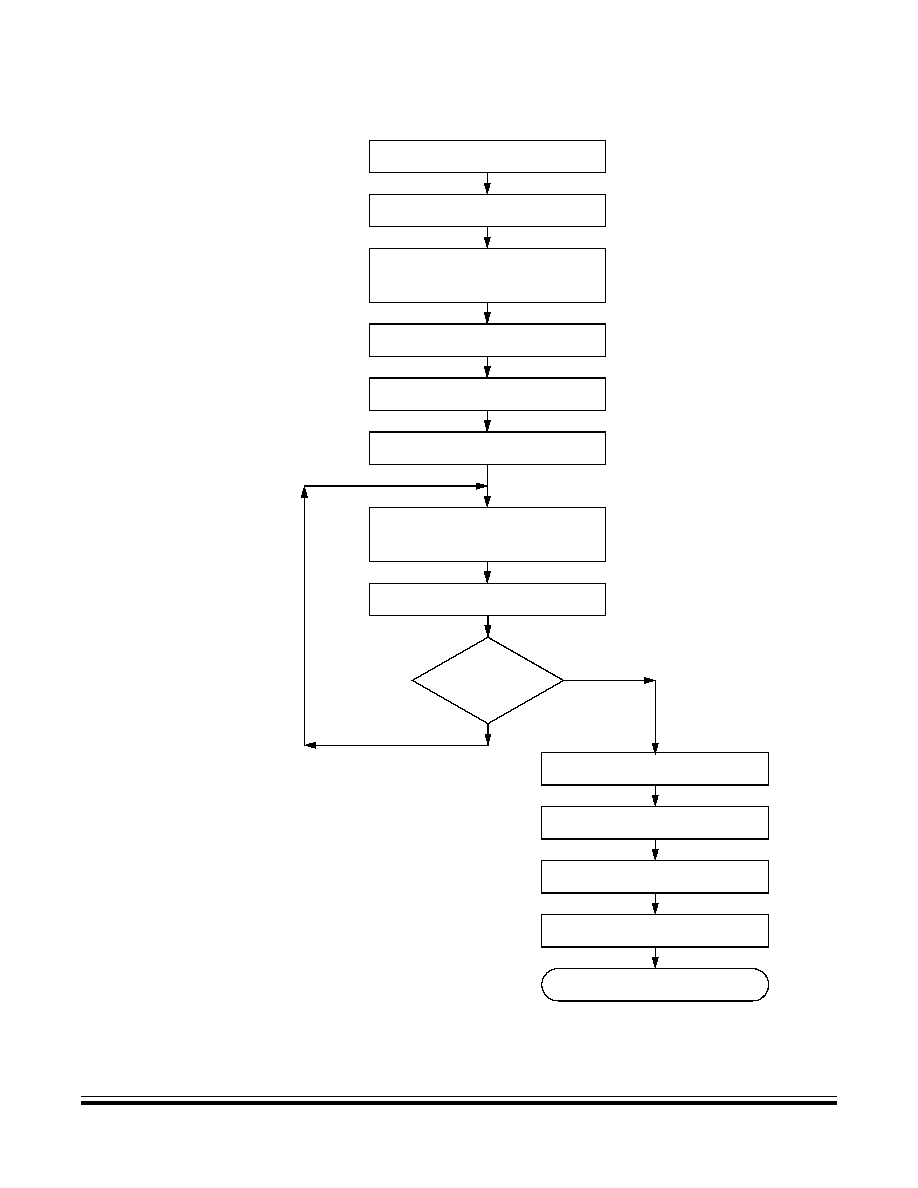
Memory
FLASH Memory (FLASH)
MC68HC908GR16 -- Rev. 1.0
Data Sheet
MOTOROLA
Memory
43
Figure 2-4. FLASH Programming Flowchart
SET HVEN BIT
READ THE FLASH BLOCK PROTECT REGISTER
WRITE ANY DATA TO ANY FLASH ADDRESS
WITHIN THE ROW ADDRESS RANGE DESIRED
WAIT FOR A TIME, t
NVS
SET PGM BIT
WAIT FOR A TIME, t
PGS
WRITE DATA TO THE FLASH ADDRESS
TO BE PROGRAMMED
WAIT FOR A TIME, t
PROG
CLEAR PGM BIT
WAIT FOR A TIME, t
NVH
CLEAR HVEN BIT
WAIT FOR A TIME, t
RCV
COMPLETED
PROGRAMMING
THIS ROW?
Y
N
END OF PROGRAMMING
The time between each FLASH address change (step 7 to step 7),
must not exceed the maximum programming
time, t
PROG
max.
or the time between the last FLASH address programmed
to clearing PGM bit (step 7 to step 10)
Note:
1
2
3
4
5
6
7
8
10
11
12
13
Algorithm for programming
a row (32 bytes) of FLASH memory
This row program algorithm assumes the row/s
to be programmed are initially erased.

Memory
Data Sheet
MC68HC908GR16 -- Rev. 1.0
44
Memory
MOTOROLA
2.6.1.5 FLASH Block Protection
Due to the ability of the on-board charge pump to erase and program the FLASH
memory in the target application, provision is made for protecting a block of
memory from unintentional erase or program operations due to system
malfunction. This protection is done by using of a FLASH block protect register
(FLBPR). The FLBPR determines the range of the FLASH memory which is to be
protected. The range of the protected area starts from a location defined by FLBPR
and ends at the bottom of the FLASH memory ($FFFF). When the memory is
protected, the HVEN bit cannot be set in either ERASE or PROGRAM operations.
NOTE:
In performing a program or erase operation, the FLASH block protect register must
be read after setting the PGM or ERASE bit and before asserting the HVEN bit
When the FLBPR is program with all 0's, the entire memory is protected from being
programmed and erased. When all the bits are erased (all 1's), the entire memory
is accessible for program and erase.
When bits within the FLBPR are programmed, they lock a block of memory,
address ranges as shown in
2.6.1.5 FLASH Block Protection
. Once the FLBPR
is programmed with a value other than $FF, any erase or program of the FLBPR or
the protected block of FLASH memory is prohibited. The presence of a V
TST
on the
IRQ pin will bypass the block protection so that all of the memory included in the
block protect register is open for program and erase operations.
NOTE:
The FLASH block protect register is not protected with special hardware or
software. Therefore, if this page is not protected by FLBPR the register is erased
by either a page or mass erase operation.
2.6.1.6 FLASH Block Protect Register
The FLASH block protect register (FLBPR) is implemented as a byte within the
FLASH memory, and therefore can only be written during a programming
sequence of the FLASH memory. The value in this register determines the starting
location of the protected range within the FLASH memory.
Address:
$FF7E
Bit 7
6
5
4
3
2
1
Bit 0
Read:
BPR7
BPR6
BPR5
BPR4
BPR3
BPR2
BPR1
BPR0
Write:
Reset:
U
U
U
U
U
U
U
U
U = Unaffected by reset. Initial value from factory is 1.
Write to this register is by a programming sequence to the FLASH memory.
Figure 2-5. FLASH Block Protect Register (FLBPR)
Memory
FLASH Memory (FLASH)
MC68HC908GR16 -- Rev. 1.0
Data Sheet
MOTOROLA
Memory
45
BPR[7:0] -- FLASH Block Protect Bits
These eight bits represent bits [13:6] of a 16-bit memory address. Bit 15 and
Bit 14 are logic 1s and bits [5:0] are logic 0s.
The resultant 16-bit address is used for specifying the start address of the
FLASH memory for block protection. The FLASH is protected from this start
address to the end of FLASH memory, at $FFFF. With this mechanism, the
protect start address can be $XX00, $XX40, $XX80, and $XXC0 (64 bytes page
boundaries) within the FLASH memory.
Figure 2-6. FLASH Block Protect Start Address
2.6.2 Wait Mode
Putting the MCU into wait mode while the FLASH is in read mode does not affect
the operation of the FLASH memory directly, but there will not be any memory
activity since the CPU is inactive.
The WAIT instruction should not be executed while performing a program or erase
operation on the FLASH, otherwise the operation will discontinue, and the FLASH
will be on standby mode.
Table 2-2. Examples of Protect Address Ranges
BPR[7:0]
Addresses of Protect Range
$00
The entire FLASH memory is protected.
$01 (0000 0001)
$C040 (1100 0000 0100 0000) -- $FFFF
$02 (0000 0010)
$C080 (1100 0000 1000 0000) -- $FFFF
$03 (0000 0011)
$C0C0 (1100 0000 1100 0000) -- $FFFF
$04 (0000 0100)
$C100 (1100 0001 0000 0000) -- $FFFF
and so on...
$FC (1111 1100)
$FF00 (1111 1111 0000 0000) -- FFFF
$FD (1111 1101)
$FF40 (1111 1111 0100 0000) -- $FFFF
FLBPR and vectors are protected
$FE (1111 1110)
$FF80 (1111 1111 1000 0000) -- FFFF
Vectors are protected
$FF
The entire FLASH memory is not protected.
1
FLBPR VALUE
16-BIT MEMORY ADDRESS
0
0
0
0
0
0
START ADDRESS OF FLASH
1
BLOCK PROTECT

Memory
Data Sheet
MC68HC908GR16 -- Rev. 1.0
46
Memory
MOTOROLA
2.6.3 Stop Mode
Putting the MCU into stop mode while the FLASH is in read mode does not affect
the operation of the FLASH memory directly, but there will not be any memory
activity since the CPU is inactive.
The STOP instruction should not be executed while performing a program or erase
operation on the FLASH, otherwise the operation will discontinue, and the FLASH
will be on standby mode
NOTE:
Standby mode is the power saving mode of the FLASH module in which all internal
control signals to the FLASH are inactive and the current consumption of the
FLASH is at a minimum.

MC68HC908GR16 -- Rev. 1.0
Data Sheet
MOTOROLA
Analog-to-Digital Converter (ADC)
47
Data Sheet -- MC68HC908GR16
Section 3. Analog-to-Digital Converter (ADC)
3.1 Introduction
This section describes the 10-bit analog-to-digital converter (ADC).
3.2 Features
Features of the ADC module include:
�
Eight channels with multiplexed input
�
Linear successive approximation with monotonicity
�
10-bit resolution
�
Single or continuous conversion
�
Conversion complete flag or conversion complete interrupt
�
Selectable ADC clock
�
Left or right justified result
�
Left justified sign data mode
3.3 Functional Description
The ADC provides eight pins for sampling external sources at pins
PTB7/AD7�PTB0/AD0. An analog multiplexer allows the single ADC converter to
select one of eight ADC channels as ADC voltage in (V
ADIN
). V
ADIN
is converted
by the successive approximation register-based analog-to-digital converter. When
the conversion is completed, ADC places the result in the ADC data register and
sets a flag or generates an interrupt. See
Figure 3-2
.
3.3.1 ADC Port I/O Pins
PTB7/AD7�PTB0/AD0 are general-purpose I/O (input/output) pins that share with
the ADC channels. The channel select bits define which ADC channel/port pin will
be used as the input signal. The ADC overrides the port I/O logic by forcing that pin
as input to the ADC. The remaining ADC channels/port pins are controlled by the
port I/O logic and can be used as general-purpose I/O. Writes to the port register
or data direction register (DDR) will not have any affect on the port pin that is
selected by the ADC. Read of a port pin in use by the ADC will return a logic 0.
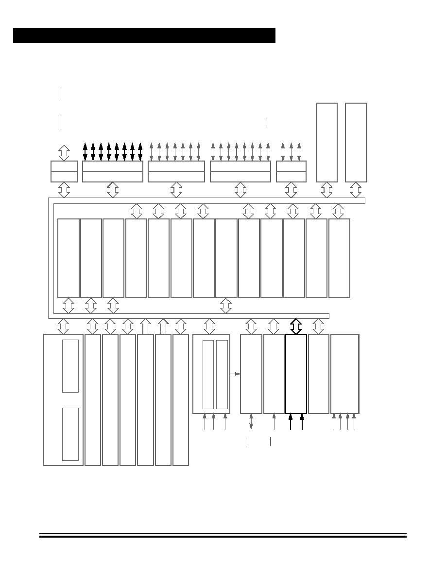
Data Sheet
MC6
8
HC90
8
GR16 --
Re
v. 1.0
48
Anal
og-to-Dig
ital Con
v
e
r
te
r (ADC)
MOTOROLA
Analog-to-Digital Con
ver
ter (ADC)
Figure 3-1. Block Diagram Highlighting ADC Block and Pins
MONITOR MODULE
M68HC08 CPU
CONTROL AND STATUS REGISTERS -- 64 BYTES
USER FLASH -- 15,872 BYTES
USER RAM -- 1024 BYTES
MONITOR ROM -- 350 BYTES
USER FLASH VECTOR SPACE -- 44 BYTES
PORTA
D
DRA
DDRC
PO
R
T
C
DDR
D
PORTD
DDRE
POR
T
E
INTERNAL BUS
OSC1
OSC2
RST
(3)
IRQ
(3)
PTA7/KBD7�PTA0/KBD0
(1)
PTB7/AD7
PTB6/AD6
PTB5/AD5
PTB4/AD4
PTB3/AD3
PTB2/AD2
PTB1/AD1
PTB0/AD0
PTC6
(1)
PTC5
(1)
PTC4
(1), (2)
PTC3
(1), (2)
PTC2
(1), (2)
PTC1
(1), (2)
PTC0
(1), (2)
PTD7/T2CH1
(1)
PTD6/T2CH0
(1)
PTD5/T1CH1
(1)
PTD4/T1CH0
(1)
PTD3/SPSCK
(1)
PTD2/MOSI
(1)
PTD1/MISO
(1)
PTD0/SS
(1)
PTE1/RxD
PTE0/TxD
SECURITY
MODULE
POWER
V
SS
V
DD
V
SSA
V
DDA
1. Ports are software configurable with pullup device if input port.
2. Higher current drive port pins
3. Pin contains integrated pullup device
MONITOR MODE ENTRY
MODULE
DDRB
PORTB
V
DDAD
/V
REFH
V
DDAD
/V
REFL
PTE5�PTE2
FLASH PROGRAMMING ROUTINES ROM -- 406 BYTES
CLOCK GENERATOR MODULE
CGMXFC
PHASE LOCKED LOOP
32�100 kHz OSCILLATOR
CPU
REGISTERS
ARITHMETIC/LOGIC
UNIT (ALU)
SYSTEM INTEGRATION
MODULE
SINGLE EXTERNAL
INTERRUPT MODULE
10-BIT ANALOG-TO-DIGITAL
CONVERTER MODULE
POWER-ON RESET
MODULE
PROGRAMMABLE TIMEBASE
MODULE
SINGLE BREAKPOINT
BREAK MODULE
DUAL VOLTAGE
LOW-VOLTAGE INHIBIT
MODULE
8-BIT KEYBOARD
INTERRUPT MODULE
2-CHANNEL TIMER
INTERFACE MODULE 1
2-CHANNEL TIMER
INTERFACE MODULE 2
ENHANCED SERIAL
COMUNICATIONS
INTERFACE MODULE
COMPUTER OPERATING
PROPERLY MODULE
SERIAL PERIPHERAL
INTERFACE MODULE
DATA BUS SWITCH
MODULE
MEMORY MAP
MODULE
CONFIGURATION
REGISTER 1�2
MODULE
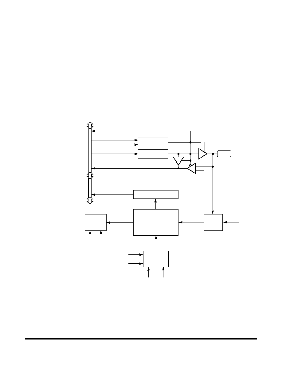
Analog-to-Digital Converter (ADC)
Functional Description
MC68HC908GR16 -- Rev. 1.0
Data Sheet
MOTOROLA
Analog-to-Digital Converter (ADC)
49
3.3.2 Voltage Conversion
When the input voltage to the ADC equals V
REFH
, the ADC converts the signal to
$3FF (full scale). If the input voltage equals V
REFL
,
the ADC converts it to $000.
Input voltages between V
REFH
and V
REFL
are a straight-line linear conversion.
NOTE:
The ADC input voltage must always be greater than V
SSA
and less than V
DDA
.
Connect the V
DDA
pin to the same voltage potential as the V
DD
pin, and connect
the V
SSA
pin to the same voltage potential as the V
SS
pin.
The V
DDA
pin should be routed carefully for maximum noise immunity.
Figure 3-2. ADC Block Diagram
INTERNAL
DATA BUS
READ DDRBx
WRITE DDRBx
RESET
WRITE PTBx
READ PTBx
PTBx
DDRBx
PTBx
INTERRUPT
LOGIC
CHANNEL
SELECT
ADC
CLOCK
GENERATOR
CONVERSION
COMPLETE
ADC
(V
ADIN
)
ADC CLOCK
CGMXCLK
BUS CLOCK
ADCH4�ADCH0
ADC DATA REGISTER
AIEN
COCO
DISABLE
DISABLE
ADC CHANNEL x
ADIV2�ADIV0
ADICLK
VOLTAGE IN

Analog-to-Digital Converter (ADC)
Data Sheet
MC68HC908GR16 -- Rev. 1.0
50
Analog-to-Digital Converter (ADC)
MOTOROLA
3.3.3 Conversion Time
Conversion starts after a write to the ADC status and control register (ADSCR).
One conversion will take between 16 and 17 ADC clock cycles. The ADIVx and
ADICLK bits should be set to provide a 1-MHz ADC clock frequency.
3.3.4 Conversion
In continuous conversion mode, the ADC data register will be filled with new data
after each conversion. Data from the previous conversion will be overwritten
whether that data has been read or not. Conversions will continue until the ADCO
bit is cleared. The COCO bit is set after the first conversion and will stay set until
the next write of the ADC status and control register or the next read of the ADC
data register.
In single conversion mode, conversion begins with a write to the ADSCR. Only one
conversion occurs between writes to the ADSCR.
3.3.5 Accuracy and Precision
The conversion process is monotonic and has no missing codes.
3.3.6 Result Justification
The conversion result may be formatted in four different ways:
1.
Left justified
2.
Right justified
3.
Left Justified sign data mode
4.
8-bit truncation mode
All four of these modes are controlled using MODE0 and MODE1 bits located in
the ADC clock register (ADCLK).
Left justification will place the eight most significant bits (MSB) in the corresponding
ADC data register high, ADRH. This may be useful if the result is to be treated as
an 8-bit result where the two least significant bits (LSB), located in the ADC data
register low, ADRL, can be ignored. However, ADRL must be read after ADRH or
else the interlocking will prevent all new conversions from being stored.
Right justification will place only the two MSBs in the corresponding ADC data
register high, ADRH, and the eight LSBs in ADC data register low, ADRL. This
mode of operation typically is used when a 10-bit unsigned result is desired.
16 to 17 ADC cycles
ADC frequency
Conversion time =
Number of bus cycles = conversion time
�
bus frequency
Analog-to-Digital Converter (ADC)
Functional Description
MC68HC908GR16 -- Rev. 1.0
Data Sheet
MOTOROLA
Analog-to-Digital Converter (ADC)
51
Left justified sign data mode is similar to left justified mode with one exception. The
MSB of the 10-bit result, AD9 located in ADRH, is complemented. This mode of
operation is useful when a result, represented as a signed magnitude from
mid-scale, is needed. Finally, 8-bit truncation mode will place the eight MSBs in the
ADC data register low, ADRL. The two LSBs are dropped. This mode of operation
is used when compatibility with 8-bit ADC designs are required. No interlocking
between ADRH and ADRL is present.
NOTE:
Quantization error is affected when only the most significant eight bits are used as
a result. See
Figure 3-3
.
Figure 3-3. Bit Truncation Mode Error
IDEAL 10-BIT CHARACTERISTIC
WITH QUANTIZATION = �1/2
IDEAL 8-BIT CHARACTERISTIC
WITH QUANTIZATION = �1/2
10-BIT TRUNCATED
TO 8-BIT RESULT
WHEN TRUNCATION IS USED,
ERROR FROM IDEAL 8-BIT = 3/8 LSB
DUE TO NON-IDEAL QUANTIZATION.
000
001
002
003
004
005
006
007
008
009
00A
00B
000
001
002
003
8-BIT
RESULT
10-BIT
RESULT
INPUT VOLTAGE
REPRESENTED AS 10-BIT
INPUT VOLTAGE
REPRESENTED AS 8-BIT
1/2
2 1/2
4 1/2
6 1/2
8 1/2
1 1/2
3 1/2
5 1/2
7 1/2
9 1/2
1/2
2 1/2
1 1/2

Analog-to-Digital Converter (ADC)
Data Sheet
MC68HC908GR16 -- Rev. 1.0
52
Analog-to-Digital Converter (ADC)
MOTOROLA
3.4 Monotonicity
The conversion process is monotonic and has no missing codes.
3.5 Interrupts
When the AIEN bit is set, the ADC module is capable of generating CPU interrupts
after each ADC conversion. A CPU interrupt is generated if the COCO bit is at
logic 0. The COCO bit is not used as a conversion complete flag when interrupts
are enabled.
3.6 Low-Power Modes
The WAIT and STOP instruction can put the MCU in low power- consumption
standby modes.
3.6.1 Wait Mode
The ADC continues normal operation during wait mode. Any enabled CPU interrupt
request from the ADC can bring the MCU out of wait mode. If the ADC is not
required to bring the MCU out of wait mode, power down the ADC by setting
ADCH4�ADCH0 bits in the ADC status and control register before executing the
WAIT instruction.
3.6.2 Stop Mode
The ADC module is inactive after the execution of a STOP instruction. Any pending
conversion is aborted. ADC conversions resume when the MCU exits stop mode
after an external interrupt. Allow one conversion cycle to stabilize the analog
circuitry.
3.7 I/O Signals
The ADC module has eight pins shared with port B, PTB7/AD7�PTB0/AD0.
3.7.1 ADC Analog Power Pin (V
DDAD
)
The ADC analog portion uses V
DDAD
as its power pin. Connect the V
DDAD
pin to
the same voltage potential as V
DD
. External filtering may be necessary to ensure
clean V
DDAD
for good results.
NOTE:
For maximum noise immunity, route V
DDAD
carefully and place bypass capacitors
as close as possible to the package.
V
DDAD
and V
REFH
are double-bonded on the MC68HC908GR16.

Analog-to-Digital Converter (ADC)
I/O Registers
MC68HC908GR16 -- Rev. 1.0
Data Sheet
MOTOROLA
Analog-to-Digital Converter (ADC)
53
3.7.2 ADC Analog Ground Pin (V
SSAD
)
The ADC analog portion uses V
SSAD
as its ground pin. Connect the V
SSAD
pin to
the same voltage potential as V
SS
.
NOTE:
Route V
SSAD
cleanly to avoid any offset errors.
V
SSAD
and V
REFL
are double-bonded on the MC68HC908GR16.
3.7.3 ADC Voltage Reference High Pin (V
REFH
)
The ADC analog portion uses V
REFH
as its upper voltage reference pin. By default,
connect the V
REFH
pin to the same voltage potential as V
DD
. External filtering is
often necessary to ensure a clean V
REFH
for good results. Any noise present on
this pin will be reflected and possibly magnified in A/D conversion values.
NOTE:
For maximum noise immunity, route V
REFH
carefully and place bypass capacitors
as close as possible to the package. Routing V
REFH
close and parallel to V
REFL
may improve common mode noise rejection.
V
DDAD
and V
REFH
are double-bonded on the MC68HC908GR16.
3.7.4 ADC Voltage Reference Low Pin (V
REFL
)
The ADC analog portion uses V
REFL
as its lower voltage reference pin. By default,
connect the V
REFH
pin to the same voltage potential as V
SS
. External filtering is
often necessary to ensure a clean V
REFL
for good results. Any noise present on this
pin will be reflected and possibly magnified in A/D conversion values.
NOTE:
For maximum noise immunity, route V
REFL
carefully and, if not connected to V
SS
,
place bypass capacitors as close as possible to the package. Routing V
REFH
close
and parallel to V
REFL
may improve common mode noise rejection.
V
SSAD
and V
REFL
are double-bonded on the MC68HC908GR16.
3.7.5 ADC Voltage In (V
ADIN
)
V
ADIN
is the input voltage signal from one of the eight ADC channels to the ADC
module.
3.8 I/O Registers
These I/O registers control and monitor ADC operation:
�
ADC status and control register (ADSCR)
�
ADC data register (ADRH and ADRL)
�
ADC clock register (ADCLK)

Analog-to-Digital Converter (ADC)
Data Sheet
MC68HC908GR16 -- Rev. 1.0
54
Analog-to-Digital Converter (ADC)
MOTOROLA
3.8.1 ADC Status and Control Register
Function of the ADC status and control register (ADSCR) is described here.
COCO -- Conversions Complete Bit
When the AIEN bit is a logic 0, the COCO is a read-only bit which is set each
time a conversion is completed except in the continuous conversion mode
where it is set after the first conversion. This bit is cleared whenever the ADSCR
is written or whenever the ADR is read.
If the AIEN bit is a logic 1, the COCO becomes a read/write bit, which should be
cleared to logic 0 for CPU to service the ADC interrupt request. Reset clears this
bit.
1 = Conversion completed (AIEN = 0)
0 = Conversion not completed (AIEN = 0)/CPU interrupt (AIEN = 1)
AIEN -- ADC Interrupt Enable Bit
When this bit is set, an interrupt is generated at the end of an ADC conversion.
The interrupt signal is cleared when the data register is read or the status/control
register is written. Reset clears the AIEN bit.
1 = ADC interrupt enabled
0 = ADC interrupt disabled
ADCO -- ADC Continuous Conversion Bit
When set, the ADC will convert samples continuously and update the ADR
register at the end of each conversion. Only one conversion is completed
between writes to the ADSCR when this bit is cleared. Reset clears the ADCO
bit.
1 = Continuous ADC conversion
0 = One ADC conversion
ADCH4�ADCH0 -- ADC Channel Select Bits
ADCH4�ADCH0 form a 5-bit field which is used to select one of 16 ADC
channels. Only eight channels, AD7�AD0, are available on this MCU. The
channels are detailed in
Table 3-1
. Care should be taken when using a port pin
as both an analog and digital input simultaneously to prevent switching noise
from corrupting the analog signal. See
Table 3-1
.
The ADC subsystem is turned off when the channel select bits are all set to 1.
This feature allows for reduced power consumption for the MCU when the ADC
is not being used.
NOTE:
Recovery from the disabled state requires one conversion cycle to stabilize.
Address:
$003C
Bit 7
6
5
4
3
2
1
Bit 0
Read:
COCO
AIEN
ADCO
ADCH4
ADCH3
ADCH2
ADCH1
ADCH0
Write:
Reset:
0
0
0
1
1
1
1
1
Figure 3-4. ADC Status and Control Register (ADSCR)
Analog-to-Digital Converter (ADC)
I/O Registers
MC68HC908GR16 -- Rev. 1.0
Data Sheet
MOTOROLA
Analog-to-Digital Converter (ADC)
55
The voltage levels supplied from internal reference nodes, as specified in
Table 3-1
, are used to verify the operation of the ADC converter both in production
test and for user applications.
3.8.2 ADC Data Register High and Data Register Low
3.8.2.1 Left Justified Mode
In left justified mode, the ADRH register holds the eight MSBs of the 10-bit result.
The only difference from left justified mode is that the AD9 is complemented. The
ADRL register holds the two LSBs of the 10-bit result. All other bits read as 0.
ADRH and ADRL are updated each time an ADC single channel conversion
completes. Reading ADRH latches the contents of ADRL until ADRL is read. All
subsequent results will be lost until the ADRH and ADRL reads are completed.
Table 3-1. Mux Channel Select
(1)
1. If any unused channels are selected, the resulting ADC conversion will be unknown or
reserved.
ADCH4
ADCH3
ADCH2
ADCH1
ADCH0
Input Select
0
0
0
0
0
PTB0/AD0
0
0
0
0
1
PTB1/AD1
0
0
0
1
0
PTB2/AD2
0
0
0
1
1
PTB3/AD3
0
0
1
0
0
PTB4/AD4
0
0
1
0
1
PTB5/AD5
0
0
1
1
0
PTB6/AD6
0
0
1
1
1
PTB7/AD7
0
1
0
0
0
Unused
1
1
1
0
0
1
1
1
0
1
V
REFH
1
1
1
1
0
V
REFL
1
1
1
1
1
ADC power off
Address:
$003D
ADRH
Bit 7
6
5
4
3
2
1
Bit 0
Read:
AD9
AD8
AD7
AD6
AD5
AD4
AD3
AD2
Write:
Reset:
Unaffected by reset
Address:
$003E
ADRL
Read:
AD1
AD0
0
0
0
0
0
0
Write:
Reset:
Unaffected by reset
= Unimplemented
Figure 3-5. ADC Data Register High (ADRH) and Low (ADRL)
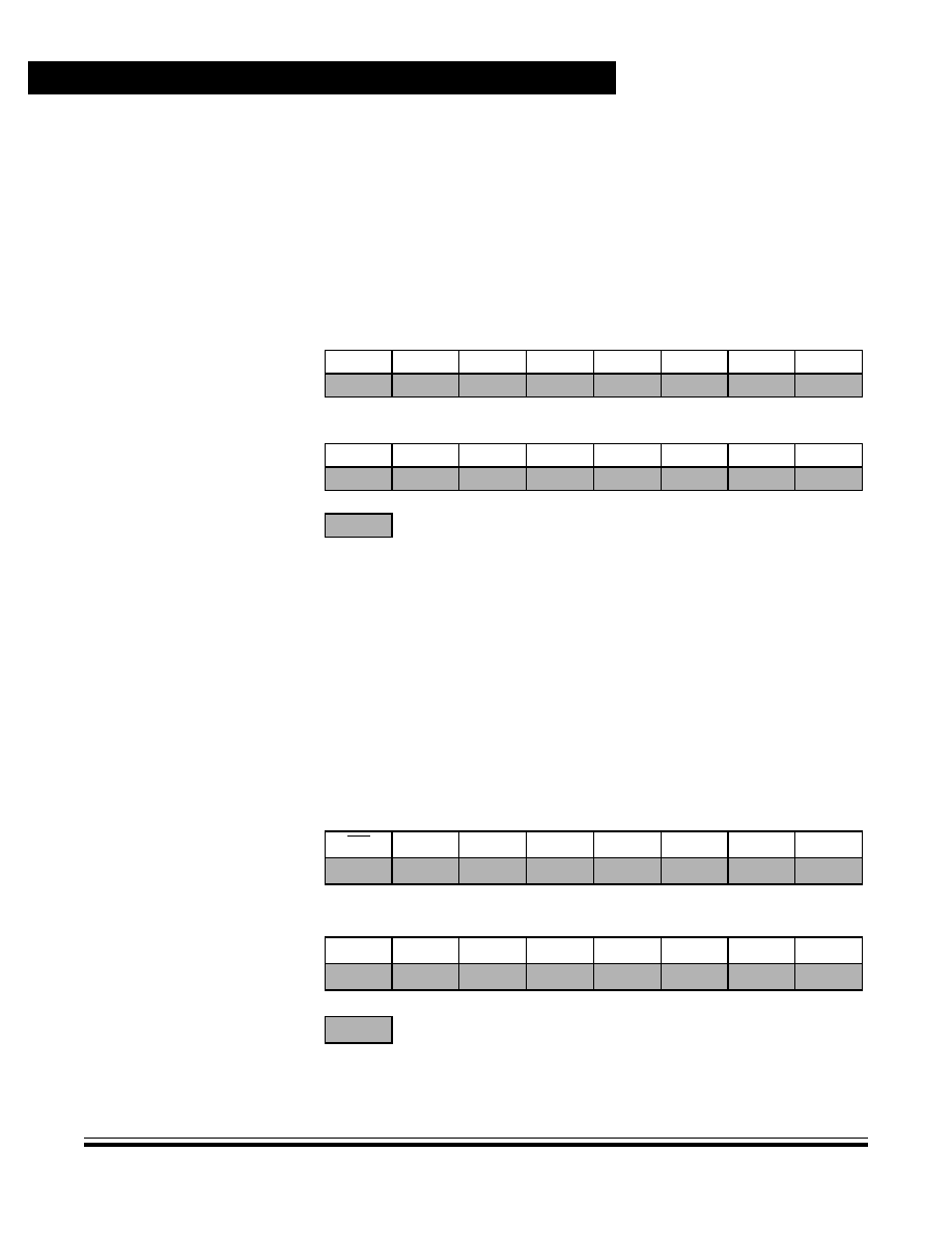
Analog-to-Digital Converter (ADC)
Data Sheet
MC68HC908GR16 -- Rev. 1.0
56
Analog-to-Digital Converter (ADC)
MOTOROLA
3.8.2.2 Right Justified Mode
In right justified mode, the ADRH register holds the two MSBs of the
10-bit result. All other bits read as 0. The ADRL register holds the eight LSBs of the
10-bit result. ADRH and ADRL are updated each time an ADC single channel
conversion completes. Reading ADRH latches the contents of ADRL until ADRL is
read. All subsequent results will be lost until the ADRH and ADRL reads are
completed.
3.8.2.3 Left Justified Signed Data Mode
In left justified signed data mode, the ADRH register holds the eight MSBs of the
10-bit result. The only difference from left justified mode is that the AD9 is
complemented. The ADRL register holds the two LSBs of the 10-bit result. All other
bits read as 0. ADRH and ADRL are updated each time an ADC single channel
conversion completes. Reading ADRH latches the contents of ADRL until ADRL is
read. All subsequent results will be lost until the ADRH and ADRL reads are
completed.
Address:
$003D
ADRH
Bit 7
6
5
4
3
2
1
Bit 0
Read:
0
0
0
0
0
0
AD9
AD8
Write:
Reset:
Unaffected by reset
Address:
$003E
ADRL
Read:
AD7
AD6
AD5
AD4
AD3
AD2
AD1
AD0
Write:
Reset:
Unaffected by reset
= Unimplemented
Figure 3-6. ADC Data Register High (ADRH) and Low (ADRL)
Address:
$003D
Bit 7
6
5
4
3
2
1
Bit 0
Read:
AD9
AD8
AD7
AD6
AD5
AD4
AD3
AD2
Write:
Reset:
Unaffected by reset
Address:
$003E
Read:
AD1
AD0
0
0
0
0
0
0
Write:
Reset:
Unaffected by reset
= Unimplemented
Figure 3-7. ADC Data Register High (ADRH) and Low (ADRL)
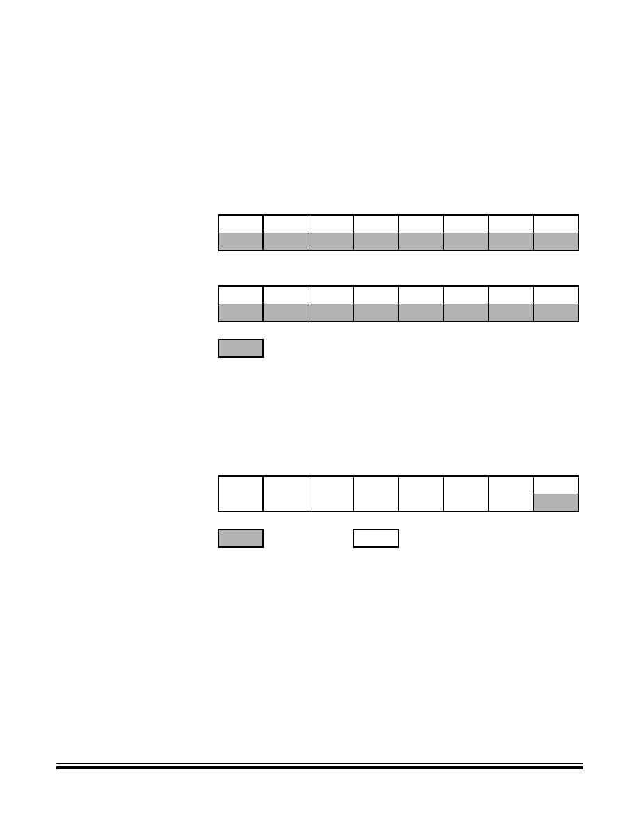
Analog-to-Digital Converter (ADC)
I/O Registers
MC68HC908GR16 -- Rev. 1.0
Data Sheet
MOTOROLA
Analog-to-Digital Converter (ADC)
57
3.8.2.4 Eight Bit Truncation Mode
In 8-bit truncation mode, the ADRL register holds the eight MSBs of the 10-bit
result. The ADRH register is unused and reads as 0. The ADRL register is updated
each time an ADC single channel conversion completes. In 8-bit mode, the ADRL
register contains no interlocking with ADRH.
3.8.3 ADC Clock Register
The ADC clock register (ADCLK) selects the clock frequency for the ADC.
ADIV2�ADIV0 -- ADC Clock Prescaler Bits
ADIV2�ADIV0 form a 3-bit field which selects the divide ratio used by the ADC
to generate the internal ADC clock.
Table 3-2
shows the available clock
configurations. The ADC clock should be set to approximately 1 MHz.
Address:
$003D
ADRH
Bit 7
6
5
4
3
2
1
Bit 0
Read:
0
0
0
0
0
0
0
0
Write:
Reset:
Unaffected by reset
Address:
$003E
ADRL
Read:
AD9
AD8
AD7
AD6
AD5
AD4
AD3
AD2
Write:
Reset:
Unaffected by reset
= Unimplemented
Figure 3-8. ADC Data Register High (ADRH) and Low (ADRL)
Address:
$003F
Bit 7
6
5
4
3
2
1
Bit 0
Read:
ADIV2
ADIV1
ADIV0
ADICLK
MODE1
MODE0
R
0
Write:
Reset:
0
0
0
0
0
1
0
0
= Unimplemented
R
= Reserved
Figure 3-9. ADC Clock Register (ADCLK)
Analog-to-Digital Converter (ADC)
Data Sheet
MC68HC908GR16 -- Rev. 1.0
58
Analog-to-Digital Converter (ADC)
MOTOROLA
ADICLK -- ADC Input Clock Select Bit
ADICLK selects either the bus clock or the oscillator output clock (CGMXCLK)
as the input clock source to generate the internal ADC clock. Reset selects
CGMXCLK as the ADC clock source.
1 = Internal bus clock
0 = Oscillator output clock (CGMXCLK)
The ADC requires a clock rate of approximately 1 MHz for correct operation. If the
selected clock source is not fast enough, the ADC will generate incorrect
conversions. See
20.13 5.0-Volt ADC Characteristics
and
20.14 3.3-Volt ADC
Characteristics
.
MODE1 and MODE0 -- Modes of Result Justification Bits
MODE1 and MODE0 select among four modes of operation. The manner in
which the ADC conversion results will be placed in the ADC data registers is
controlled by these modes of operation. Reset returns right-justified mode.
00 = 8-bit truncation mode
01 = Right justified mode
10 = Left justified mode
11 = Left justified signed data mode
Table 3-2. ADC Clock Divide Ratio
ADIV2
ADIV1
ADIV0
ADC Clock Rate
0
0
0
ADC input clock
�
1
0
0
1
ADC input clock
�
2
0
1
0
ADC input clock
�
4
0
1
1
ADC input clock
�
8
1
X
(1)
1. X = Don't care
X
(1)
ADC input clock
�
16
f
ADIC
=
f
CGMXCLK
or bus frequency
ADIV[2:0]
1 MHz

MC68HC908GR16 -- Rev. 1.0
Data Sheet
MOTOROLA
Clock Generator Module (CGM)
59
Data Sheet -- MC68HC908GR16
Section 4. Clock Generator Module (CGM)
4.1 Introduction
This section describes the clock generator module. The CGM generates the crystal
clock signal, CGMXCLK, which operates at the frequency of the crystal. The CGM
also generates the base clock signal, CGMOUT, which is based on either the
crystal clock divided by two or the phase-locked loop (PLL) clock, CGMVCLK,
divided by two. In user mode, CGMOUT is the clock from which the SIM derives
the system clocks, including the bus clock, which is at a frequency of CGMOUT/2.
In monitor mode, PTC3 determines the bus clock. The PLL is a fully functional
frequency generator designed for use with crystals or ceramic resonators. The PLL
can generate an 8-MHz bus frequency using a
32-kHz crystal.
4.2 Features
Features of the CGM include:
�
Phase-locked loop with output frequency in integer multiples of an integer
dividend of the crystal reference
�
Low-frequency crystal operation with low-power operation and high-output
frequency resolution
�
Programmable prescaler for power-of-two increases in frequency
�
Programmable hardware voltage-controlled oscillator (VCO) for low-jitter
operation
�
Automatic bandwidth control mode for low-jitter operation
�
Automatic frequency lock detector
�
CPU interrupt on entry or exit from locked condition
�
Configuration register bit to allow oscillator operation during stop mode
4.3 Functional Description
The CGM consists of three major submodules:
�
Crystal oscillator circuit -- The crystal oscillator circuit generates the
constant crystal frequency clock, CGMXCLK.
�
Phase-locked loop (PLL) -- The PLL generates the programmable VCO
frequency clock, CGMVCLK.
�
Base clock selector circuit -- This software-controlled circuit selects either
CGMXCLK divided by two or the VCO clock, CGMVCLK, divided by two as
the base clock, CGMOUT. The SIM derives the system clocks from either
CGMOUT or CGMXCLK.

Clock Generator Module (CGM)
Data Sheet
MC68HC908GR16 -- Rev. 1.0
60
Clock Generator Module (CGM)
MOTOROLA
Figure 4-1
shows the structure of the CGM.
Figure 4-1. CGM Block Diagram
BCS
PHASE
DETECTOR
LOOP
FILTER
FREQUENCY
DIVIDER
VOLTAGE
CONTROLLED
OSCILLATOR
AUTOMATIC
MODE
CONTROL
LOCK
DETECTOR
CLOCK
CGMXCLK
CGMOUT
CGMVDV
CGMVCLK
SIMOSCEN (FROM SIM)
OSCILLATOR (OSC)
INTERRUPT
CONTROL
CGMINT
CGMRDV
PLL ANALOG
� 2
CGMRCLK
OSC2
OSC1
SELECT
CIRCUIT
V
DDA
CGMXFC
V
SSA
LOCK
AUTO
ACQ
VPR1�VPR0
PLLIE
PLLF
MUL11�MUL0
REFERENCE
DIVIDER
VRS7�VRS0
FREQUENCY
DIVIDER
PRE1�PRE0
OSCSTOPENB
(FROM CONFIG)
(TO: SIM, TIMTB15A, ADC)
PHASE-LOCKED LOOP (PLL)
(TO SIM)
(TO SIM)
RDS3�RDS0

Clock Generator Module (CGM)
Functional Description
MC68HC908GR16 -- Rev. 1.0
Data Sheet
MOTOROLA
Clock Generator Module (CGM)
61
4.3.1 Crystal Oscillator Circuit
The crystal oscillator circuit consists of an inverting amplifier and an external
crystal. The OSC1 pin is the input to the amplifier and the OSC2 pin is the output.
The SIMOSCEN signal from the system integration module (SIM) or the
OSCSTOPENB bit in the CONFIG register enable the crystal oscillator circuit.
The CGMXCLK signal is the output of the crystal oscillator circuit and runs at a rate
equal to the crystal frequency. CGMXCLK is then buffered to produce CGMRCLK,
the PLL reference clock.
CGMXCLK can be used by other modules which require precise timing for
operation. The duty cycle of CGMXCLK is not guaranteed to be 50% and depends
on external factors, including the crystal and related external components. An
externally generated clock also can feed the OSC1 pin of the crystal oscillator
circuit. Connect the external clock to the OSC1 pin and let the OSC2 pin float.
4.3.2 Phase-Locked Loop Circuit (PLL)
The PLL is a frequency generator that can operate in either acquisition mode or
tracking mode, depending on the accuracy of the output frequency. The PLL can
change between acquisition and tracking modes either automatically or manually.
4.3.3 PLL Circuits
The PLL consists of these circuits:
�
Voltage-controlled oscillator (VCO)
�
Reference divider
�
Frequency prescaler
�
Modulo VCO frequency divider
�
Phase detector
�
Loop filter
�
Lock detector
The operating range of the VCO is programmable for a wide range of frequencies
and for maximum immunity to external noise, including supply and CGM/XFC
noise. The VCO frequency is bound to a range from roughly one-half to twice the
center-of-range frequency, f
VRS
. Modulating the voltage on the CGM/XFC pin
changes the frequency within this range. By design, f
VRS
is equal to the nominal
center-of-range frequency, f
NOM
, (38.4 kHz) times a linear factor, L, and a
power-of-two factor, E, or (L
�
2
E
)f
NOM
.
CGMRCLK is the PLL reference clock, a buffered version of CGMXCLK.
CGMRCLK runs at a frequency, f
RCLK
, and is fed to the PLL through a
programmable modulo reference divider, which divides f
RCLK
by a factor, R. The
divider's output is the final reference clock, CGMRDV, running at a frequency,
f
RDV
= f
RCLK
/R. With an external crystal (30 kHz�100 kHz), always set R = 1 for

Clock Generator Module (CGM)
Data Sheet
MC68HC908GR16 -- Rev. 1.0
62
Clock Generator Module (CGM)
MOTOROLA
specified performance. With an external high-frequency clock source, use R to
divide the external frequency to between 30 kHz and 100 kHz.
The VCO's output clock, CGMVCLK, running at a frequency, f
VCLK
, is fed back
through a programmable prescale divider and a programmable modulo divider.
The prescaler divides the VCO clock by a power-of-two factor P and the modulo
divider reduces the VCO clock by a factor, N. The dividers' output is the VCO
feedback clock, CGMVDV, running at a frequency, f
VDV
= f
VCLK
/(N
�
2
P
). (See
4.3.6 Programming the PLL
for more information.)
The phase detector then compares the VCO feedback clock, CGMVDV, with the
final reference clock, CGMRDV. A correction pulse is generated based on the
phase difference between the two signals. The loop filter then slightly alters the DC
voltage on the external capacitor connected to CGMXFC based on the width and
direction of the correction pulse. The filter can make fast or slow corrections
depending on its mode, described in
4.3.4 Acquisition and Tracking Modes
. The
value of the external capacitor and the reference frequency determine the speed
of the corrections and the stability of the PLL.
The lock detector compares the frequencies of the VCO feedback clock, CGMVDV,
and the final reference clock, CGMRDV. Therefore, the speed of the lock detector
is directly proportional to the final reference frequency, f
RDV
. The circuit determines
the mode of the PLL and the lock condition based on this comparison.
4.3.4 Acquisition and Tracking Modes
The PLL filter is manually or automatically configurable into one of two operating
modes:
�
Acquisition mode -- In acquisition mode, the filter can make large frequency
corrections to the VCO. This mode is used at PLL startup or when the PLL
has suffered a severe noise hit and the VCO frequency is far off the desired
frequency. When in acquisition mode, the ACQ bit is clear in the PLL
bandwidth control register. (See
4.5.2 PLL Bandwidth Control Register
.)
�
Tracking mode -- In tracking mode, the filter makes only small corrections
to the frequency of the VCO. PLL jitter is much lower in tracking mode, but
the response to noise is also slower. The PLL enters tracking mode when
the VCO frequency is nearly correct, such as when the PLL is selected as
the base clock source. (See
4.3.8 Base Clock Selector Circuit
.) The PLL
is automatically in tracking mode when not in acquisition mode or when the
ACQ bit is set.

Clock Generator Module (CGM)
Functional Description
MC68HC908GR16 -- Rev. 1.0
Data Sheet
MOTOROLA
Clock Generator Module (CGM)
63
4.3.5 Manual and Automatic PLL Bandwidth Modes
The PLL can change the bandwidth or operational mode of the loop filter manually
or automatically. Automatic mode is recommended for most users.
In automatic bandwidth control mode (AUTO = 1), the lock detector automatically
switches between acquisition and tracking modes. Automatic bandwidth control
mode also is used to determine when the VCO clock, CGMVCLK, is safe to use as
the source for the base clock, CGMOUT. (See
4.5.2 PLL Bandwidth Control
Register
.) If PLL interrupts are enabled, the software can wait for a PLL interrupt
request and then check the LOCK bit. If interrupts are disabled, software can poll
the LOCK bit continuously (during PLL startup, usually) or at periodic intervals. In
either case, when the LOCK bit is set, the VCO clock is safe to use as the source
for the base clock. (See
4.3.8 Base Clock Selector Circuit
.) If the VCO is selected
as the source for the base clock and the LOCK bit is clear, the PLL has suffered a
severe noise hit and the software must take appropriate action, depending on the
application. (See
4.6 Interrupts
for information and precautions on using
interrupts.)
The following conditions apply when the PLL is in automatic bandwidth control
mode:
�
The ACQ bit (see
4.5.2 PLL Bandwidth Control Register
) is a read-only
indicator of the mode of the filter. (See
4.3.4 Acquisition and Tracking
Modes
.)
�
The ACQ bit is set when the VCO frequency is within a certain tolerance and
is cleared when the VCO frequency is out of a certain tolerance. (See
4.8
Acquisition/Lock Time Specifications
for more information.)
�
The LOCK bit is a read-only indicator of the locked state of the PLL.
�
The LOCK bit is set when the VCO frequency is within a certain tolerance
and is cleared when the VCO frequency is out of a certain tolerance. (See
4.8 Acquisition/Lock Time Specifications
for more information.)
�
CPU interrupts can occur if enabled (PLLIE = 1) when the PLL's lock
condition changes, toggling the LOCK bit. (See
4.5.1 PLL Control
Register
.)
The PLL also may operate in manual mode (AUTO = 0). Manual mode is used by
systems that do not require an indicator of the lock condition for proper operation.
Such systems typically operate well below f
BUSMAX
.
The following conditions apply when in manual mode:
�
ACQ is a writable control bit that controls the mode of the filter. Before
turning on the PLL in manual mode, the ACQ bit must be clear.
�
Before entering tracking mode (ACQ = 1), software must wait a given time,
t
ACQ
(see
4.8 Acquisition/Lock Time Specifications
), after turning on the
PLL by setting PLLON in the PLL control register (PCTL).

Clock Generator Module (CGM)
Data Sheet
MC68HC908GR16 -- Rev. 1.0
64
Clock Generator Module (CGM)
MOTOROLA
�
Software must wait a given time, t
AL
, after entering tracking mode before
selecting the PLL as the clock source to CGMOUT (BCS = 1).
�
The LOCK bit is disabled.
�
CPU interrupts from the CGM are disabled.
4.3.6 Programming the PLL
The following procedure shows how to program the PLL.
NOTE:
The round function in the following equations means that the real number should
be rounded to the nearest integer number.
1.
Choose the desired bus frequency, f
BUSDES
.
2.
Calculate the desired VCO frequency (four times the desired bus
frequency).
3.
Choose a practical PLL (crystal) reference frequency, f
RCLK
, and the
reference clock divider, R. Typically, the reference crystal is 32.768 kHz and
R = 1.
Frequency errors to the PLL are corrected at a rate of f
RCLK
/R. For stability
and lock time reduction, this rate must be as fast as possible. The VCO
frequency must be an integer multiple of this rate. The relationship between
the VCO frequency, f
VCLK
, and the reference frequency, f
RCLK
,
is
P, the power of two multiplier, and N, the range multiplier, are integers.
In cases where desired bus frequency has some tolerance, choose f
RCLK
to
a value determined either by other module requirements (such as modules
which are clocked by CGMXCLK), cost requirements, or ideally, as high as
the specified range allows. See
Section 20. Electrical Specifications
.
Choose the reference divider, R = 1. After choosing N and P, the actual bus
frequency can be determined using equation in 2 above.
When the tolerance on the bus frequency is tight, choose f
RCLK
to an integer
divisor of f
BUSDES
, and R = 1. If f
RCLK
cannot meet this requirement, use the
following equation to solve for R with
practical choices of f
RCLK
, and choose the f
RCLK
that gives the lowest R.
f
VCLKDES
4
f
BUSDES
�
=
f
VCLK
2
P
N
R
----------- f
RCLK
(
)
=
R
round R
MAX
f
VCLKDES
f
RCLK
--------------------------
integer
f
VCLKDES
f
RCLK
--------------------------
�
�
=
Clock Generator Module (CGM)
Functional Description
MC68HC908GR16 -- Rev. 1.0
Data Sheet
MOTOROLA
Clock Generator Module (CGM)
65
4.
Select a VCO frequency multiplier, N.
Reduce N/R to the lowest possible R.
5.
If N is < N
max
, use P = 0. If N > N
max
, choose P using this table:
Then recalculate N:
6.
Calculate and verify the adequacy of the VCO and bus frequencies f
VCLK
and f
BUS
.
7.
Select the VCO's power-of-two range multiplier E, according to this table:
8.
Select a VCO linear range multiplier, L, where f
NOM
= 38.4 kHz
Current N Value
P
0
1
2
3
Frequency Range
E
(1)
1. Do not program E to a value of 3.
0 < f
VCLK
< 8 MHz
0
8 MHz
f
VCLK
< 16 MHz
1
16 MHz
f
VCLK
< 32 MHz
2
N
round
R
f
VCLKDES
�
f
RCLK
-------------------------------------
=
0
N
<
N
max
N
max
N
<
N
max
2
�
N
max
2
�
N
<
N
max
4
�
N
max
4
�
N
<
N
max
8
�
N
round
R
f
VCLKDES
�
f
RCLK
2
P
�
-------------------------------------
=
f
VCLK
2
P
N R
/
�
(
)
f
RCLK
�
=
f
BUS
f
VCLK
(
)
4
/
=
L
round
n
f
VCLK
2
E
f
NOM
�
--------------------------
=

Clock Generator Module (CGM)
Data Sheet
MC68HC908GR16 -- Rev. 1.0
66
Clock Generator Module (CGM)
MOTOROLA
9.
Calculate and verify the adequacy of the VCO programmed center-of-range
frequency, f
VRS
. The center-of-range frequency is the midpoint between the
minimum and maximum frequencies attainable by the PLL.
For proper operation,
10.
Verify the choice of P, R, N, E, and L by comparing f
VCLK
to f
VRS
and
f
VCLKDES
. For proper operation, f
VCLK
must be within the application's
tolerance of f
VCLKDES
, and f
VRS
must be as close as possible to f
VCLK
.
NOTE:
Exceeding the recommended maximum bus frequency or VCO frequency can
crash the MCU.
11.
Program the PLL registers accordingly:
a.
In the PRE bits of the PLL control register (PCTL), program the binary
equivalent of P.
b.
In the VPR bits of the PLL control register (PCTL), program the binary
equivalent of E.
c.
In the PLL multiplier select register low (PMSL) and the PLL multiplier
select register high (PMSH), program the binary equivalent of N.
d.
In the PLL VCO range select register (PMRS), program the binary
coded equivalent of L.
e.
In the PLL reference divider select register (PMDS), program the
binary coded equivalent of R.
Table 4-1
provides numeric examples (numbers are in hexadecimal notation):
f
VRS
L
2
E
�
(
)
f
NOM
=
f
VRS
f
VCLK
�
f
NOM
2
E
�
2
--------------------------
Table 4-1. Numeric Example
f
BUS
f
RCLK
R
N
P
E
L
2.0 MHz
32.768 kHz
1
F5
0
0
D1
2.4576 MHz
32.768 kHz
1
12C
0
1
80
2.5 MHz
32.768 kHz
1
132
0
1
83
4.0 MHz
32.768 kHz
1
1E9
0
1
D1
4.9152 MHz
32.768 kHz
1
258
0
2
80
5.0 MHz
32.768 kHz
1
263
0
2
82
7.3728 MHz
32.768 kHz
1
384
0
2
C0
8.0 MHz
32.768 kHz
1
3D1
0
2
D0

Clock Generator Module (CGM)
Functional Description
MC68HC908GR16 -- Rev. 1.0
Data Sheet
MOTOROLA
Clock Generator Module (CGM)
67
4.3.7 Special Programming Exceptions
The programming method described in
4.3.6 Programming the PLL
does not
account for three possible exceptions. A value of 0 for R, N, or L is meaningless
when used in the equations given. To account for these exceptions:
�
A 0 value for R or N is interpreted exactly the same as a value of 1.
�
A 0 value for L disables the PLL and prevents its selection as the source for
the base clock.
See
4.3.8 Base Clock Selector Circuit
.
4.3.8 Base Clock Selector Circuit
This circuit is used to select either the crystal clock, CGMXCLK, or the VCO clock,
CGMVCLK, as the source of the base clock, CGMOUT. The two input clocks go
through a transition control circuit that waits up to three CGMXCLK cycles and
three CGMVCLK cycles to change from one clock source to the other. During this
time, CGMOUT is held in stasis. The output of the transition control circuit is then
divided by two to correct the duty cycle. Therefore, the bus clock frequency, which
is one-half of the base clock frequency, is one-fourth the frequency of the selected
clock (CGMXCLK or CGMVCLK).
The BCS bit in the PLL control register (PCTL) selects which clock drives
CGMOUT. The VCO clock cannot be selected as the base clock source if the PLL
is not turned on. The PLL cannot be turned off if the VCO clock is selected. The
PLL cannot be turned on or off simultaneously with the selection or deselection of
the VCO clock. The VCO clock also cannot be selected as the base clock source
if the factor L is programmed to a 0. This value would set up a condition
inconsistent with the operation of the PLL, so that the PLL would be disabled and
the crystal clock would be forced as the source of the base clock.
4.3.9 CGM External Connections
In its typical configuration, the CGM requires up to nine external components. Five
of these are for the crystal oscillator and two or four are for the PLL.
The crystal oscillator is normally connected in a Pierce oscillator configuration, as
shown in
Figure 4-2
.
Figure 4-2
shows only the logical representation of the
internal components and may not represent actual circuitry. The oscillator
configuration uses five components:
�
Crystal, X
1
�
Fixed capacitor, C
1
�
Tuning capacitor, C
2
(can also be a fixed capacitor)
�
Feedback resistor, R
B
�
Series resistor, R
S

Clock Generator Module (CGM)
Data Sheet
MC68HC908GR16 -- Rev. 1.0
68
Clock Generator Module (CGM)
MOTOROLA
The series resistor (R
S
) is included in the diagram to follow strict Pierce oscillator
guidelines. Refer to the crystal manufacturer's data for more information regarding
values for C1 and C2.
Figure 4-2
also shows the external components for the PLL:
�
Bypass capacitor, C
BYP
�
Filter network
Routing should be done with great care to minimize signal cross talk and noise.
See
20.12 Clock Generation Module Characteristics
for capacitor and resistor
values.
Figure 4-2. CGM External Connections
OSC1
C1
C2
SIMOSCEN
CGMXCLK
R
B
X1
R
S
C
BYP
OSC2
CGMXFC
V
DDA
Note: Filter network in box can be replaced with a single capacitor, but will degrade stability.
V
DD
OSCSTOPENB
(FROM CONFIG)
R
F1
C
F2
C
F1
V
SSA

Clock Generator Module (CGM)
I/O Signals
MC68HC908GR16 -- Rev. 1.0
Data Sheet
MOTOROLA
Clock Generator Module (CGM)
69
4.4 I/O Signals
The following paragraphs describe the CGM I/O signals.
4.4.1 Crystal Amplifier Input Pin (OSC1)
The OSC1 pin is an input to the crystal oscillator amplifier.
4.4.2 Crystal Amplifier Output Pin (OSC2)
The OSC2 pin is the output of the crystal oscillator inverting amplifier.
4.4.3 External Filter Capacitor Pin (CGMXFC)
The CGMXFC pin is required by the loop filter to filter out phase corrections. An
external filter network is connected to this pin. (See
Figure 4-2
.)
NOTE:
To prevent noise problems, the filter network should be placed as close to the
CGMXFC pin as possible, with minimum routing distances and no routing of other
signals across the network.
4.4.4 PLL Analog Power Pin (V
DDA
)
V
DDA
is a power pin used by the analog portions of the PLL. Connect the V
DDA
pin
to the same voltage potential as the V
DD
pin.
NOTE:
Route V
DDA
carefully for maximum noise immunity and place bypass capacitors as
close as possible to the package.
4.4.5 PLL Analog Ground Pin (V
SSA
)
V
SSA
is a ground pin used by the analog portions of the PLL. Connect the V
SSA
pin
to the same voltage potential as the V
SS
pin.
NOTE:
Route V
SSA
carefully for maximum noise immunity and place bypass capacitors as
close as possible to the package.
4.4.6 Oscillator Enable Signal (SIMOSCEN)
The SIMOSCEN signal comes from the system integration module (SIM) and
enables the oscillator and PLL.
4.4.7 Oscillator Stop Mode Enable Bit (OSCSTOPENB)
OSCSTOPENB is a bit in the CONFIG register that enables the oscillator to
continue operating during stop mode. If this bit is set, the Oscillator continues
running during stop mode. If this bit is not set (default), the oscillator is controlled
by the SIMOSCEN signal which will disable the oscillator during stop mode.

Clock Generator Module (CGM)
Data Sheet
MC68HC908GR16 -- Rev. 1.0
70
Clock Generator Module (CGM)
MOTOROLA
4.4.8 Crystal Output Frequency Signal (CGMXCLK)
CGMXCLK is the crystal oscillator output signal. It runs at the full speed of the
crystal (f
XCLK
) and comes directly from the crystal oscillator circuit.
Figure 4-2
shows only the logical relation of CGMXCLK to OSC1 and OSC2 and may not
represent the actual circuitry. The duty cycle of CGMXCLK is unknown and may
depend on the crystal and other external factors. Also, the frequency and amplitude
of CGMXCLK can be unstable at startup.
4.4.9 CGM Base Clock Output (CGMOUT)
CGMOUT is the clock output of the CGM. This signal goes to the SIM, which
generates the MCU clocks. CGMOUT is a 50 percent duty cycle clock running at
twice the bus frequency. CGMOUT is software programmable to be either the
oscillator output, CGMXCLK, divided by two or the VCO clock, CGMVCLK, divided
by two.
4.4.10 CGM CPU Interrupt (CGMINT)
CGMINT is the interrupt signal generated by the PLL lock detector.
4.5 CGM Registers
These registers control and monitor operation of the CGM:
�
PLL control register (PCTL)
(See
4.5.1 PLL Control Register
.)
�
PLL bandwidth control register (PBWC)
(See
4.5.2 PLL Bandwidth Control Register
.)
�
PLL multiplier select register high (PMSH)
(See
4.5.3 PLL Multiplier Select Register High
.)
�
PLL multiplier select register low (PMSL)
(See
4.5.4 PLL Multiplier Select Register Low
.)
�
PLL VCO range select register (PMRS)
(See
4.5.5 PLL VCO Range Select Register
.)
�
PLL reference divider select register (PMDS)
(See
4.5.6 PLL Reference Divider Select Register
.)
Figure 4-3
is a summary of the CGM registers.
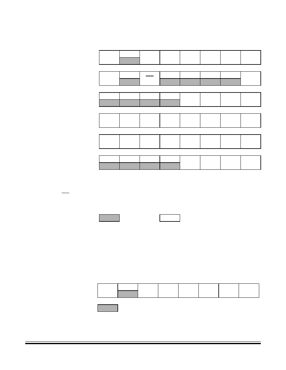
Clock Generator Module (CGM)
CGM Registers
MC68HC908GR16 -- Rev. 1.0
Data Sheet
MOTOROLA
Clock Generator Module (CGM)
71
4.5.1 PLL Control Register
The PLL control register (PCTL) contains the interrupt enable and flag bits, the
on/off switch, the base clock selector bit, the prescaler bits, and the VCO
power-of-two range selector bits.
Addr.
Register Name
Bit 7
6
5
4
3
2
1
Bit 0
$0036
PLL Control Register (PCTL)
See page 71.
Read:
PLLIE
PLLF
PLLON
BCS
PRE1
PRE0
VPR1
VPR0
Write:
Reset:
0
0
1
0
0
0
0
0
$0037
PLL Bandwidth Control Reg-
ister (PBWC)
See page 73.
Read:
AUTO
LOCK
ACQ
0
0
0
0
R
Write:
Reset:
0
0
0
0
0
0
0
0
$0038
PLL Multiplier Select High
Register (PMSH)
See page 74.
Read:
0
0
0
0
MUL11
MUL10
MUL9
MUL8
Write:
Reset:
0
0
0
0
0
0
0
0
$0039
PLL Multiplier Select Low
Register (PMSL)
See page 75.
Read:
MUL7
MUL6
MUL5
MUL4
MUL3
MUL2
MUL1
MUL0
Write:
Reset:
0
1
0
0
0
0
0
0
$003A
PLL VCO Select Range
Register (PMRS)
See page 75.
Read:
VRS7
VRS6
VRS5
VRS4
VRS3
VRS2
VRS1
VRS0
Write:
Reset:
0
1
0
0
0
0
0
0
$003B
PLL Reference Divider
Select Register (PMDS)
See page 76.
Read:
0
0
0
0
RDS3
RDS2
RDS1
RDS0
Write:
Reset:
0
0
0
0
0
0
0
1
NOTES:
1. When AUTO = 0, PLLIE is forced clear and is read-only.
2. When AUTO = 0, PLLF and LOCK read as clear.
3. When AUTO = 1, ACQ is read-only.
4. When PLLON = 0 or VRS7:VRS0 = $0, BCS is forced clear and is read-only.
5. When PLLON = 1, the PLL programming register is read-only.
6. When BCS = 1, PLLON is forced set and is read-only.
= Unimplemented
R
= Reserved
Figure 4-3. CGM I/O Register Summary
Address:
$0036
Bit 7
6
5
4
3
2
1
Bit 0
Read:
PLLIE
PLLF
PLLON
BCS
PRE1
PRE0
VPR1
VPR0
Write:
Reset:
0
0
1
0
0
0
0
0
= Unimplemented
Figure 4-4. PLL Control Register (PCTL)

Clock Generator Module (CGM)
Data Sheet
MC68HC908GR16 -- Rev. 1.0
72
Clock Generator Module (CGM)
MOTOROLA
PLLIE -- PLL Interrupt Enable Bit
This read/write bit enables the PLL to generate an interrupt request when the
LOCK bit toggles, setting the PLL flag, PLLF. When the AUTO bit in the PLL
bandwidth control register (PBWC) is clear, PLLIE cannot be written and reads
as logic 0. Reset clears the PLLIE bit.
1 = PLL interrupts enabled
0 = PLL interrupts disabled
PLLF -- PLL Interrupt Flag Bit
This read-only bit is set whenever the LOCK bit toggles. PLLF generates an
interrupt request if the PLLIE bit also is set. PLLF always reads as logic 0 when
the AUTO bit in the PLL bandwidth control register (PBWC) is clear. Clear the
PLLF bit by reading the PLL control register. Reset clears the PLLF bit.
1 = Change in lock condition
0 = No change in lock condition
NOTE:
Do not inadvertently clear the PLLF bit. Any read or read-modify-write operation on
the PLL control register clears the PLLF bit.
PLLON -- PLL On Bit
This read/write bit activates the PLL and enables the VCO clock, CGMVCLK.
PLLON cannot be cleared if the VCO clock is driving the base clock, CGMOUT
(BCS = 1). (See
4.3.8 Base Clock Selector Circuit
.) Reset sets this bit so that
the loop can stabilize as the MCU is powering up.
1 = PLL on
0 = PLL off
BCS -- Base Clock Select Bit
This read/write bit selects either the crystal oscillator output, CGMXCLK, or the
VCO clock, CGMVCLK, as the source of the CGM output, CGMOUT. CGMOUT
frequency is one-half the frequency of the selected clock. BCS cannot be set
while the PLLON bit is clear. After toggling BCS, it may take up to three
CGMXCLK and three CGMVCLK cycles to complete the transition from one
source clock to the other. During the transition, CGMOUT is held in stasis. (See
4.3.8 Base Clock Selector Circuit
.) Reset clears the BCS bit.
1 = CGMVCLK divided by two drives CGMOUT
0 = CGMXCLK divided by two drives CGMOUT
NOTE:
PLLON and BCS have built-in protection that prevents the base clock selector
circuit from selecting the VCO clock as the source of the base clock if the PLL is
off. Therefore, PLLON cannot be cleared when BCS is set, and BCS cannot be set
when PLLON is clear. If the PLL is off (PLLON = 0), selecting CGMVCLK requires
two writes to the PLL control register. (See
4.3.8 Base Clock Selector Circuit
.)
PRE1 and PRE0 -- Prescaler Program Bits
These read/write bits control a prescaler that selects the prescaler power-of-two
multiplier, P. (See
4.3.3 PLL Circuits
and
4.3.6 Programming the PLL
.) PRE1
and PRE0 cannot be written when the PLLON bit is set. Reset clears these bits.
NOTE:
The value of P is normally 0 when using a 32.768-kHz crystal as the reference.

Clock Generator Module (CGM)
CGM Registers
MC68HC908GR16 -- Rev. 1.0
Data Sheet
MOTOROLA
Clock Generator Module (CGM)
73
VPR1 and VPR0 -- VCO Power-of-Two Range Select Bits
These read/write bits control the VCO's hardware power-of-two range multiplier
E that, in conjunction with L (See
4.3.3 PLL Circuits
,
4.3.6 Programming the
PLL
, and
4.5.5 PLL VCO Range Select Register
.) controls the hardware
center-of-range frequency, f
VRS
. VPR1:VPR0 cannot be written when the
PLLON bit is set. Reset clears these bits.
4.5.2 PLL
Bandwidth Control Register
The PLL bandwidth control register (PBWC):
�
Selects automatic or manual (software-controlled) bandwidth control mode
�
Indicates when the PLL is locked
�
In automatic bandwidth control mode, indicates when the PLL is in
acquisition or tracking mode
In manual operation, forces the PLL into acquisition or tracking mode
Table 4-2. PRE1 and PRE0 Programming
PRE1 and PRE0
P
Prescaler Multiplier
00
0
1
01
1
2
10
2
4
11
3
8
Table 4-3. VPR1 and VPR0 Programming
VPR1 and VPR0
E
VCO Power-of-Two
Range Multiplier
00
0
1
01
1
2
10
2
4
11
3
(1)
1. Do not program E to a value of 3.
8
Address:
$0037
Bit 7
6
5
4
3
2
1
Bit 0
Read:
AUTO
LOCK
ACQ
0
0
0
0
R
Write:
Reset:
0
0
0
0
0
0
0
0
= Unimplemented
R
= Reserved
Figure 4-5. PLL Bandwidth Control Register (PBWC)
Clock Generator Module (CGM)
Data Sheet
MC68HC908GR16 -- Rev. 1.0
74
Clock Generator Module (CGM)
MOTOROLA
AUTO -- Automatic Bandwidth Control Bit
This read/write bit selects automatic or manual bandwidth control. When
initializing the PLL for manual operation (AUTO = 0), clear the ACQ bit before
turning on the PLL. Reset clears the AUTO bit.
1 = Automatic bandwidth control
0 = Manual bandwidth control
LOCK -- Lock Indicator Bit
When the AUTO bit is set, LOCK is a read-only bit that becomes set when the
VCO clock, CGMVCLK, is locked (running at the programmed frequency).
When the AUTO bit is clear, LOCK reads as logic 0 and has no meaning. The
write one function of this bit is reserved for test, so this bit must always be
written a 0. Reset clears the LOCK bit.
1 = VCO frequency correct or locked
0 = VCO frequency incorrect or unlocked
ACQ -- Acquisition Mode Bit
When the AUTO bit is set, ACQ is a read-only bit that indicates whether the PLL
is in acquisition mode or tracking mode. When the AUTO bit is clear, ACQ is a
read/write bit that controls whether the PLL is in acquisition or tracking mode.
In automatic bandwidth control mode (AUTO = 1), the last-written value from
manual operation is stored in a temporary location and is recovered when
manual operation resumes. Reset clears this bit, enabling acquisition mode.
1 = Tracking mode
0 = Acquisition mode
4.5.3 PLL Multiplier Select Register High
The PLL multiplier select register high (PMSH) contains the programming
information for the high byte of the modulo feedback divider.
MUL11�MUL8 -- Multiplier Select Bits
These read/write bits control the high byte of the modulo feedback divider that
selects the VCO frequency multiplier N. (See
4.3.3 PLL Circuits
and
4.3.6
Programming the PLL
.) A value of $0000 in the multiplier select registers
configures the modulo feedback divider the same as a value of $0001. Reset
initializes the registers to $0040 for a default multiply value of 64.
NOTE:
The multiplier select bits have built-in protection such that they cannot be written
when the PLL is on (PLLON = 1).
Address:
$0038
Bit 7
6
5
4
3
2
1
Bit 0
Read:
0
0
0
0
MUL11
MUL10
MUL9
MUL8
Write:
Reset:
0
0
0
0
0
0
0
0
= Unimplemented
Figure 4-6. PLL Multiplier Select Register High (PMSH)

Clock Generator Module (CGM)
CGM Registers
MC68HC908GR16 -- Rev. 1.0
Data Sheet
MOTOROLA
Clock Generator Module (CGM)
75
PMSH[7:4] -- Unimplemented Bits
These bits have no function and always read as logic 0s.
4.5.4 PLL Multiplier Select Register Low
The PLL multiplier select register low (PMSL) contains the programming
information for the low byte of the modulo feedback divider.
MUL7�MUL0 -- Multiplier Select Bits
These read/write bits control the low byte of the modulo feedback divider that
selects the VCO frequency multiplier, N. (See
4.3.3 PLL Circuits
and
4.3.6
Programming the PLL
.) MUL7�MUL0 cannot be written when the PLLON bit
in the PCTL is set. A value of $0000 in the multiplier select registers configures
the modulo feedback divider the same as a value of $0001. Reset initializes the
register to $40 for a default multiply value of 64.
NOTE:
The multiplier select bits have built-in protection such that they cannot be written
when the PLL is on (PLLON = 1).
4.5.5 PLL VCO Range Select Register
NOTE:
PMRS may be called PVRS on other HC08 derivatives.
The PLL VCO range select register (PMRS) contains the programming information
required for the hardware configuration of the VCO.
VRS7�VRS0 -- VCO Range Select Bits
These read/write bits control the hardware center-of-range linear multiplier L
which, in conjunction with E (see
4.3.3 PLL Circuits
,
4.3.6 Programming the
PLL
, and
4.5.1 PLL Control Register
), controls the hardware center-of-range
frequency, f
VRS
. VRS7�VRS0 cannot be written when the PLLON bit in the
PCTL is set. (See
4.3.7 Special Programming Exceptions
.)
A value of $00 in
the VCO range select register disables the PLL and clears the BCS bit in the
Address:
$0038
Bit 7
6
5
4
3
2
1
Bit 0
Read:
MUL7
MUL6
MUL5
MUL4
MUL3
MUL2
MUL1
MUL0
Write:
Reset:
0
1
0
0
0
0
0
0
Figure 4-7. PLL Multiplier Select Register Low (PMSL)
Address:
$003A
Bit 7
6
5
4
3
2
1
Bit 0
Read:
VRS7
VRS6
VRS5
VRS4
VRS3
VRS2
VRS1
VRS0
Write:
Reset:
0
1
0
0
0
0
0
0
Figure 4-8. PLL VCO Range Select Register (PMRS)
Clock Generator Module (CGM)
Data Sheet
MC68HC908GR16 -- Rev. 1.0
76
Clock Generator Module (CGM)
MOTOROLA
PLL control register (PCTL). (See
4.3.8 Base Clock Selector Circuit
and
4.3.7
Special Programming Exceptions
.) Reset initializes the register to $40 for a
default range multiply value of 64.
NOTE:
The VCO range select bits have built-in protection such that they cannot be written
when the PLL is on (PLLON = 1) and such that the VCO clock cannot be selected
as the source of the base clock (BCS = 1) if the VCO range select bits are all clear.
The PLL VCO range select register must be programmed correctly. Incorrect
programming can result in failure of the PLL to achieve lock.
4.5.6 PLL Reference Divider Select Register
NOTE:
PMDS may be called PRDS on other HC08 derivatives.
The PLL reference divider select register (PMDS) contains the programming
information for the modulo reference divider.
RDS3�RDS0 -- Reference Divider Select Bits
These read/write bits control the modulo reference divider that selects the
reference division factor, R. (See
4.3.3 PLL Circuits
and
4.3.6 Programming
the PLL
.) RDS7�RDS0 cannot be written when the PLLON bit in the PCTL is
set. A value of $00 in the reference divider select register configures the
reference divider the same as a value of $01. (See
4.3.7 Special Programming
Exceptions
.) Reset initializes the register to $01 for a default divide value of 1.
NOTE:
The reference divider select bits have built-in protection such that they cannot be
written when the PLL is on (PLLON = 1).
NOTE:
The default divide value of 1 is recommended for all applications.
PMDS7�PMDS4 -- Unimplemented Bits
These bits have no function and always read as logic 0s.
4.6 Interrupts
When the AUTO bit is set in the PLL bandwidth control register (PBWC), the PLL
can generate a CPU interrupt request every time the LOCK bit changes state. The
PLLIE bit in the PLL control register (PCTL) enables CPU interrupts from the PLL.
PLLF, the interrupt flag in the PCTL, becomes set whether interrupts are enabled
Address:
$003B
Bit 7
6
5
4
3
2
1
Bit 0
Read:
0
0
0
0
RDS3
RDS2
RDS1
RDS0
Write:
Reset:
0
0
0
0
0
0
0
1
= Unimplemented
Figure 4-9. PLL Reference Divider Select Register (PMDS)

Clock Generator Module (CGM)
Special Modes
MC68HC908GR16 -- Rev. 1.0
Data Sheet
MOTOROLA
Clock Generator Module (CGM)
77
or not. When the AUTO bit is clear, CPU interrupts from the PLL are disabled and
PLLF reads as logic 0.
Software should read the LOCK bit after a PLL interrupt request to see if the
request was due to an entry into lock or an exit from lock. When the PLL enters
lock, the VCO clock, CGMVCLK, divided by two can be selected as the CGMOUT
source by setting BCS in the PCTL. When the PLL exits lock, the VCO clock
frequency is corrupt, and appropriate precautions should be taken. If the
application is not frequency sensitive, interrupts should be disabled to prevent PLL
interrupt service routines from impeding software performance or from exceeding
stack limitations.
NOTE:
Software can select the CGMVCLK divided by two as the CGMOUT source even
if the PLL is not locked (LOCK = 0). Therefore, software should make sure the PLL
is locked before setting the BCS bit.
4.7 Special Modes
The WAIT instruction puts the MCU in low power-consumption standby modes.
4.7.1 Wait Mode
The WAIT instruction does not affect the CGM. Before entering wait mode,
software can disengage and turn off the PLL by clearing the BCS and PLLON bits
in the PLL control register (PCTL) to save power. Less power-sensitive
applications can disengage the PLL without turning it off, so that the PLL clock is
immediately available at WAIT exit. This would be the case also when the PLL is
to wake the MCU from wait mode, such as when the PLL is first enabled and
waiting for LOCK or LOCK is lost.
4.7.2 Stop Mode
If the OSCSTOPENB bit in the CONFIG register is cleared (default), then the
STOP instruction disables the CGM (oscillator and phase locked loop) and holds
low all CGM outputs (CGMXCLK, CGMOUT, and CGMINT).
If the STOP instruction is executed with the VCO clock, CGMVCLK, divided by two
driving CGMOUT, the PLL automatically clears the BCS bit in the PLL control
register (PCTL), thereby selecting the crystal clock, CGMXCLK, divided by two as
the source of CGMOUT. When the MCU recovers from STOP, the crystal clock
divided by two drives CGMOUT and BCS remains clear.
If the OSCSTOPENB bit in the CONFIG register is set, then the phase locked loop
is shut off but the oscillator will continue to operate in stop mode.

Clock Generator Module (CGM)
Data Sheet
MC68HC908GR16 -- Rev. 1.0
78
Clock Generator Module (CGM)
MOTOROLA
4.7.3 CGM During Break Interrupts
The system integration module (SIM) controls whether status bits in other modules
can be cleared during the break state. The BCFE bit in the SIM break flag control
register (SBFCR) enables software to clear status bits during the break state. (See
Section 15. System Integration Module (SIM)
.)
To allow software to clear status bits during a break interrupt, write a logic 1 to the
BCFE bit. If a status bit is cleared during the break state, it remains cleared when
the MCU exits the break state.
To protect the PLLF bit during the break state, write a logic 0 to the BCFE bit. With
BCFE at logic 0 (its default state), software can read and write the PLL control
register during the break state without affecting the PLLF bit.
4.8 Acquisition/Lock Time Specifications
The acquisition and lock times of the PLL are, in many applications, the most
critical PLL design parameters. Proper design and use of the PLL ensures the
highest stability and lowest acquisition/lock times.
4.8.1 Acquisition/Lock Time Definitions
Typical control systems refer to the acquisition time or lock time as the reaction
time, within specified tolerances, of the system to a step input. In a PLL, the step
input occurs when the PLL is turned on or when it suffers a noise hit. The tolerance
is usually specified as a percentage of the step input or when the output settles to
the desired value plus or minus a percentage of the frequency change. Therefore,
the reaction time is constant in this definition, regardless of the size of the step
input. For example, consider a system with a 5 percent acquisition time tolerance.
If a command instructs the system to change from 0 Hz to 1 MHz, the acquisition
time is the time taken for the frequency to reach 1 MHz
�
50 kHz. Fifty kHz = 5% of
the 1-MHz step input. If the system is operating at 1 MHz and suffers a �100-kHz
noise hit, the acquisition time is the time taken to return from 900 kHz to
1 MHz
�
5 kHz. Five kHz = 5% of the 100-kHz step input.
Other systems refer to acquisition and lock times as the time the system takes to
reduce the error between the actual output and the desired output to within
specified tolerances. Therefore, the acquisition or lock time varies according to the
original error in the output. Minor errors may not even be registered. Typical PLL
applications prefer to use this definition because the system requires the output
frequency to be within a certain tolerance of the desired frequency regardless of
the size of the initial error.

Clock Generator Module (CGM)
Acquisition/Lock Time Specifications
MC68HC908GR16 -- Rev. 1.0
Data Sheet
MOTOROLA
Clock Generator Module (CGM)
79
4.8.2 Parametric Influences on Reaction Time
Acquisition and lock times are designed to be as short as possible while still
providing the highest possible stability. These reaction times are not constant,
however. Many factors directly and indirectly affect the acquisition time.
The most critical parameter which affects the reaction times of the PLL is the
reference frequency, f
RDV
. This frequency is the input to the phase detector and
controls how often the PLL makes corrections. For stability, the corrections must
be small compared to the desired frequency, so several corrections are required to
reduce the frequency error. Therefore, the slower the reference the longer it takes
to make these corrections. This parameter is under user control via the choice of
crystal frequency f
XCLK
and the R value programmed in the reference divider. (See
4.3.3 PLL Circuits
,
4.3.6 Programming the PLL
, and
4.5.6 PLL Reference
Divider Select Register
.)
Another critical parameter is the external filter network. The PLL modifies the
voltage on the VCO by adding or subtracting charge from capacitors in this
network. Therefore, the rate at which the voltage changes for a given frequency
error (thus change in charge) is proportional to the capacitance. The size of the
capacitor also is related to the stability of the PLL. If the capacitor is too small, the
PLL cannot make small enough adjustments to the voltage and the system cannot
lock. If the capacitor is too large, the PLL may not be able to adjust the voltage in
a reasonable time. (See
4.8.3 Choosing a Filter
.)
Also important is the operating voltage potential applied to V
DDA
. The power supply
potential alters the characteristics of the PLL. A fixed value is best. Variable
supplies, such as batteries, are acceptable if they vary within a known range at very
slow speeds. Noise on the power supply is not acceptable, because it causes small
frequency errors which continually change the acquisition time of the PLL.
Temperature and processing also can affect acquisition time because the electrical
characteristics of the PLL change. The part operates as specified as long as these
influences stay within the specified limits. External factors, however, can cause
drastic changes in the operation of the PLL. These factors include noise injected
into the PLL through the filter capacitor, filter capacitor leakage, stray impedances
on the circuit board, and even humidity or circuit board contamination.
Clock Generator Module (CGM)
Data Sheet
MC68HC908GR16 -- Rev. 1.0
80
Clock Generator Module (CGM)
MOTOROLA
4.8.3 Choosing a Filter
As described in
4.8.2 Parametric Influences on Reaction Time
, the external filter
network is critical to the stability and reaction time of the PLL. The PLL is also
dependent on reference frequency and supply voltage.
Figure 4-10
shows two types of filter circuits. In low-cost applications, where
stability and reaction time of the PLL are not critical, the three component filter
network of
Figure 4-10
(B) can be replaced by a single capacitor, C
F
, shown in
Figure 4-10
(A). Refer to
Table 4-4
for recommended filter components at various
reference frequencies. For reference frequencies between the values listed in the
table, extrapolate to the nearest common capacitor value. In general, a slightly
larger capacitor provides more stability at the expense of increased lock time.
Figure 4-10. PLL Filter
Table 4-4. Example Filter Component Values
f
RCLK
C
F1
C
F2
R
F1
C
F
32 kHz
0.15
�
F
15 nF
2 K
0.22
�
F
40 kHz
0.12
�
F
12 nF
2 K
0.18
�
F
50 kHz
0.10
�
F
10 nF
2 K
0.18
�
F
60 kHz
82 nF
8.2 nF
2 K
0.12
�
F
70 kHz
68 nF
6.8 nF
2 K
0.12
�
F
80 kHz
56 nF
5.6 nF
2 K
0.1
�
F
90 kHz
56 nF
5.6 nF
2 K
0.1
�
F
100 kHz
47 nF
4.7 nF
2 K
82 nF
CGMXFC
R
F1
C
F2
C
F1
V
SSA
CGMXFC
C
F
V
SSA
(A)
(B)

MC68HC908GR16 -- Rev. 1.0
Data Sheet
MOTOROLA
Configuration Register (CONFIG)
81
Data Sheet -- MC68HC908GR16
Section 5. Configuration Register (CONFIG)
5.1 Introduction
This section describes the configuration registers, CONFIG1 and CONFIG2. The
configuration registers enable or disable these options:
�
Stop mode recovery time (32 CGMXCLK cycles or 4096 CGMXCLK cycles)
�
COP timeout period (2
18
� 2
4
or 2
13
� 2
4
COPCLK cycles)
�
STOP instruction
�
Computer operating properly module (COP)
�
Low-voltage inhibit (LVI) module control and voltage trip point selection
�
Enable/disable the oscillator (OSC) during stop mode
�
Enable/disable an extra divide by 128 prescaler in timebase module
5.2 Functional Description
The configuration registers are used in the initialization of various options. The
configuration registers can be written once after each reset. All of the configuration
register bits are cleared during reset. Since the various options affect the operation
of the microcontroller unit (MCU), it is recommended that these registers be written
immediately after reset. The configuration registers are located at $001E and
$001F and may be read at anytime.
NOTE:
On a FLASH device, the options except LVI5OR3 are one-time writable by the user
after each reset. The LVI5OR3 bit is one-time writable by the user only after each
POR (power-on reset). The CONFIG registers are not in the FLASH memory but
are special registers containing one-time writable latches after each reset. Upon
a reset, the CONFIG registers default to predetermined settings as shown in
Figure 5-1
and
Figure 5-2
.
Configuration Register (CONFIG)
Data Sheet
MC68HC908GR16 -- Rev. 1.0
82
Configuration Register (CONFIG)
MOTOROLA
TMCLKSEL-- Timebase Clock Select Bit
TMCLKSEL enables an extra divide-by-128 prescaler in the timebase module.
Setting this bit enables the extra prescaler and clearing this bit disables it. See
Section 4. Clock Generator Module (CGM)
for a more detailed description of
the external clock operation.
1 = Enables extra divide-by-128 prescaler in timebase module
0 = Disables extra divide-by-128 prescaler in timebase module
OSCENINSTOP -- Oscillator Enable In Stop Mode Bit
OSCENINSTOP, when set, will enable oscillator to continue to generate clocks
in stop mode. See
Section 4. Clock Generator Module (CGM)
. This function
is used to keep the timebase running while the reset of the MCU stops. See
Section 17. Timebase Module (TBM)
. When clear, oscillator will cease to
generate clocks while in stop mode. The default state for this option is clear,
disabling the oscillator in stop mode.
1 = Oscillator enabled to operate during stop mode
0 = Oscillator disabled during stop mode (default)
SCIBDSRC -- SCI Baud Rate Clock Source Bit
SCIBDSRC controls the clock source used for the serial communications
interface (SCI). The setting of this bit affects the frequency at which the SCI
operates.See
Section 14. Enhanced Serial Communications Interface
(ESCI) Module
.
1 = Internal data bus clock used as clock source for SCI (default)
0 = External oscillator used as clock source for SCI
Address:
$001E
Bit 7
6
5
4
3
2
1
Bit 0
Read:
0
0
0
0
R
TMCLK-
SEL
OSCEN-
INSTOP
SCIBD-
SRC
Write:
Reset:
0
0
0
0
0
0
0
1
= Unimplemented
R
= Reserved
Figure 5-1. Configuration Register 2 (CONFIG2)
Address:
$001F
Bit 7
6
5
4
3
2
1
Bit 0
Read:
COPRS
LVISTOP
LVIRSTD
LVIPWRD
LVI5OR3
SSREC
STOP
COPD
Write:
Reset:
0
0
0
0
See note
0
0
0
Note: LVI5OR3 bit is only reset via POR (power-on reset)
Figure 5-2. Configuration Register 1 (CONFIG1)

Configuration Register (CONFIG)
Functional Description
MC68HC908GR16 -- Rev. 1.0
Data Sheet
MOTOROLA
Configuration Register (CONFIG)
83
COPRS -- COP Rate Select Bit
COPD selects the COP timeout period. Reset clears COPRS. See
Section 6.
Computer Operating Properly (COP) Module
1 = COP timeout period = 2
13
� 2
4
COPCLK cycles
0 = COP timeout period = 2
18
� 2
4
COPCLK cycles
LVISTOP -- LVI Enable in Stop Mode Bit
When the LVIPWRD bit is clear, setting the LVISTOP bit enables the LVI to
operate during stop mode. Reset clears LVISTOP.
1 = LVI enabled during stop mode
0 = LVI disabled during stop mode
LVIRSTD -- LVI Reset Disable Bit
LVIRSTD disables the reset signal from the LVI module. See
Section 11.
Low-Voltage Inhibit (LVI)
.
1 = LVI module resets disabled
0 = LVI module resets enabled
LVIPWRD -- LVI Power Disable Bit
LVIPWRD disables the LVI module. See
Section 11. Low-Voltage Inhibit
(LVI)
.
1 = LVI module power disabled
0 = LVI module power enabled
LVI5OR3 -- LVI 5-V or 3-V Operating Mode Bit
LVI5OR3 selects the voltage operating mode of the LVI module (see
Section
11. Low-Voltage Inhibit (LVI)
). The voltage mode selected for the LVI should
match the operating V
DD
(see
Section 20. Electrical Specifications
) for the
LVI's voltage trip points for each of the modes.
1 = LVI operates in 5-V mode
0 = LVI operates in 3-V mode
NOTE:
The LVI5OR3 bit is cleared by a power-on reset (POR) only. Other resets will leave
this bit unaffected.
SSREC -- Short Stop Recovery Bit
SSREC enables the CPU to exit stop mode with a delay of 32 CGMXCLK cycles
instead of a 4096-CGMXCLK cycle delay.
1 = Stop mode recovery after 32 CGMXCLK cycles
0 = Stop mode recovery after 4096 CGMXCLCK cycles
NOTE:
Exiting stop mode by an LVI reset will result in the long stop recovery.
If the system clock source selected is the internal oscillator or the external
crystal and the OSCENINSTOP configuration bit is not set, the oscillator will be
disabled during stop mode. The short stop recovery does not provide enough
time for oscillator stabilization and for this reason the SSREC bit should not
be set.

Configuration Register (CONFIG)
Data Sheet
MC68HC908GR16 -- Rev. 1.0
84
Configuration Register (CONFIG)
MOTOROLA
When using the LVI during normal operation but disabling during stop mode, the
LVI will have an enable time of t
EN
. The system stabilization time for power-on
reset and long stop recovery (both 4096 CGMXCLK cycles) gives a delay longer
than the LVI enable time for these startup scenarios. There is no period where
the MCU is not protected from a low-power condition. However, when using the
short stop recovery configuration option, the 32-CGMXCLK delay must be
greater than the LVI's turn on time to avoid a period in startup where the LVI is
not protecting the MCU.
STOP -- STOP Instruction Enable Bit
STOP enables the STOP instruction.
1 = STOP instruction enabled
0 = STOP instruction treated as illegal opcode
COPD -- COP Disable Bit
COPD disables the COP module. See
Section 6. Computer Operating
Properly (COP) Module
.
1 = COP module disabled
0 = COP module enabled
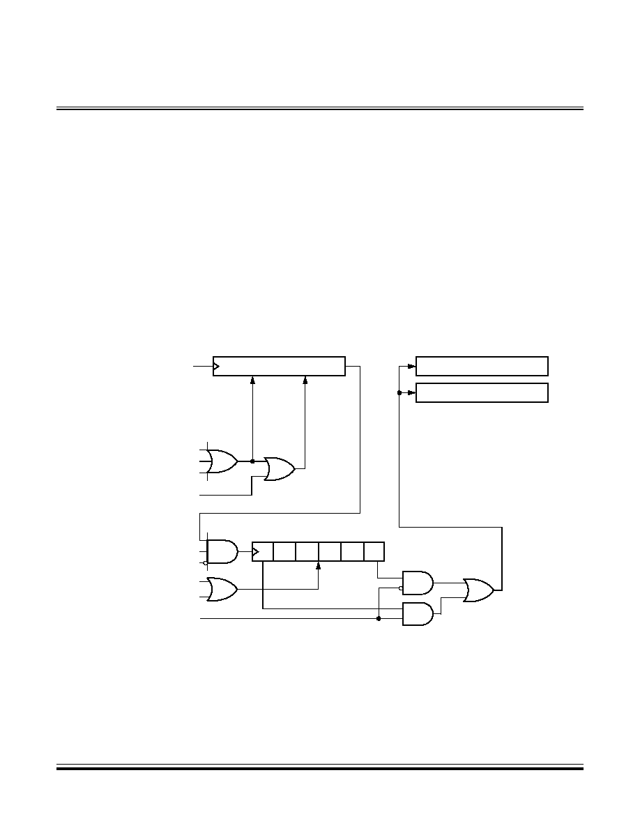
MC68HC908GR16 -- Rev. 1.0
Data Sheet
MOTOROLA
Computer Operating Properly (COP) Module
85
Data Sheet -- MC68HC908GR16
Section 6. Computer Operating Properly (COP) Module
6.1 Introduction
The computer operating properly (COP) module contains a free-running counter
that generates a reset if allowed to overflow. The COP module helps software
recover from runaway code. Prevent a COP reset by clearing the COP counter
periodically. The COP module can be disabled through the COPD bit in the
CONFIG register.
6.2 Functional Description
Figure 6-1
shows the structure of the COP module.
Figure 6-1. COP Block Diagram
COPCTL WRITE
CGMXCLK
RESET VECTOR FETCH
RESET CIRCUIT
RESET STATUS REGISTER
INTERNAL RESET SOURCES
12-BIT COP PRESCALER
CLEAR ALL
STA
G
ES
6-BIT COP COUNTER
COP DISABLE
RESET
COPCTL WRITE
CLEAR
COP MODULE
COPEN (FROM SIM)
COP COUNTER
COP CLOCK
COP TIMEOUT
STOP INSTRUCTION
(FROM CONFIG)
COP RATE SEL
(FROM CONFIG)
CL
EAR STAGES 5�1
2

Computer Operating Properly (COP) Module
Data Sheet
MC68HC908GR16 -- Rev. 1.0
86
Computer Operating Properly (COP) Module
MOTOROLA
The COP counter is a free-running 6-bit counter preceded by a 12-bit prescaler
counter. If not cleared by software, the COP counter overflows and generates an
asynchronous reset after 2
18
� 2
4
or 2
13
� 2
4
CGMXCLK cycles, depending on the
state of the COP rate select bit, COPRS, in the configuration register. With a
2
13
� 2
4
CGMXCLK cycle overflow option, a 4.9152-MHz crystal gives a COP
timeout period of 53.3 ms. Writing any value to location $FFFF before an overflow
occurs prevents a COP reset by clearing the COP counter and stages 12�5 of the
prescaler.
NOTE:
Service the COP immediately after reset and before entering or after exiting stop
mode to guarantee the maximum time before the first COP counter overflow.
A COP reset pulls the RST pin low for 32 CGMXCLK cycles and sets the COP bit
in the reset status register (RSR).
In monitor mode, the COP is disabled if the RST pin or the IRQ1 is held at V
TST
.
During the break state, V
TST
on the RST pin disables the COP.
NOTE:
Place COP clearing instructions in the main program and not in an interrupt
subroutine. Such an interrupt subroutine could keep the COP from generating a
reset even while the main program is not working properly.
6.3 I/O Signals
The following paragraphs describe the signals shown in
Figure 6-1
.
6.3.1 CGMXCLK
CGMXCLK is the crystal oscillator output signal. CGMXCLK frequency is equal to
the crystal frequency.
6.3.2 STOP Instruction
The STOP instruction clears the COP prescaler.
6.3.3 COPCTL Write
Writing any value to the COP control register (COPCTL) clears the COP counter
and clears bits 12�5 of the prescaler. Reading the COP control register returns the
low byte of the reset vector. See
6.4 COP Control Register.
6.3.4 Power-On Reset
The power-on reset (POR) circuit clears the COP prescaler 4096 CGMXCLK
cycles after power-up.

Computer Operating Properly (COP) Module
COP Control Register
MC68HC908GR16 -- Rev. 1.0
Data Sheet
MOTOROLA
Computer Operating Properly (COP) Module
87
6.3.5 Internal Reset
An internal reset clears the COP prescaler and the COP counter.
6.3.6 Reset Vector Fetch
A reset vector fetch occurs when the vector address appears on the data bus. A
reset vector fetch clears the COP prescaler.
6.3.7 COPD (COP Disable)
The COPD signal reflects the state of the COP disable bit (COPD) in the
configuration register. See
Section 5. Configuration Register (CONFIG).
6.3.8 COPRS (COP Rate Select)
The COPRS signal reflects the state of the COP rate select bit (COPRS) in the
configuration register. See
Section 5. Configuration Register (CONFIG).
6.4 COP Control Register
The COP control register (COPCTL) is located at address $FFFF and overlaps the
reset vector. Writing any value to $FFFF clears the COP counter and starts a new
timeout period. Reading location $FFFF returns the low byte of the reset vector.
6.5 Interrupts
The COP does not generate central processor unit (CPU) interrupt requests.
6.6 Monitor Mode
When monitor mode is entered with V
TST
on the IRQ pin, the COP is disabled as
long as V
TST
remains on the IRQ pin or the RST pin. When monitor mode is
entered by having blank reset vectors and not having V
TST
on the IRQ pin, the COP
is automatically disabled until a POR occurs.
Address: $FFFF
Bit 7
6
5
4
3
2
1
Bit 0
Read:
Low byte of reset vector
Write:
Clear COP counter
Reset:
Unaffected by reset
Figure 6-2. COP Control Register (COPCTL)

Computer Operating Properly (COP) Module
Data Sheet
MC68HC908GR16 -- Rev. 1.0
88
Computer Operating Properly (COP) Module
MOTOROLA
6.7 Low-Power Modes
The WAIT and STOP instructions put the microcontroller unit (MCU) in low
power-consumption standby modes.
6.7.1 Wait Mode
The COP remains active during wait mode. If COP is enabled, a reset will occur at
COP timeout.
6.7.2 Stop Mode
Stop mode turns off the CGMXCLK input to the COP and clears the COP prescaler.
Service the COP immediately before entering or after exiting stop mode to ensure
a full COP timeout period after entering or exiting stop mode.
To prevent inadvertently turning off the COP with a STOP instruction, a
configuration option is available that disables the STOP instruction. When the
STOP bit in the configuration register has the STOP instruction disabled, execution
of a STOP instruction results in an illegal opcode reset.
6.8 COP Module During Break Mode
The COP is disabled during a break interrupt when V
TST
is present on the RST pin.

MC68HC908GR16 -- Rev. 1.0
Data Sheet
MOTOROLA
Central Processor Unit (CPU)
89
Data Sheet -- MC68HC908GR16
Section 7. Central Processor Unit (CPU)
7.1 Introduction
The M68HC08 CPU (central processor unit) is an enhanced and fully
object-code-compatible version of the M68HC05 CPU. The CPU08 Reference
Manual (Motorola document order number CPU08RM/AD) contains a description
of the CPU instruction set, addressing modes, and architecture.
7.2 Features
Features of the CPU include:
�
Object code fully upward-compatible with M68HC05 Family
�
16-bit stack pointer with stack manipulation instructions
�
16-bit index register with x-register manipulation instructions
�
8-MHz CPU internal bus frequency
�
64-Kbyte program/data memory space
�
16 addressing modes
�
Memory-to-memory data moves without using accumulator
�
Fast 8-bit by 8-bit multiply and 16-bit by 8-bit divide instructions
�
Enhanced binary-coded decimal (BCD) data handling
�
Modular architecture with expandable internal bus definition for extension of
addressing range beyond 64 Kbytes
�
Low-power stop and wait modes
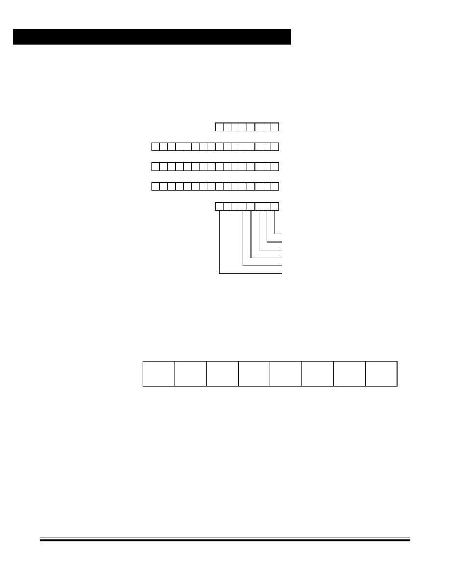
Central Processor Unit (CPU)
Data Sheet
MC68HC908GR16 -- Rev. 1.0
90
Central Processor Unit (CPU)
MOTOROLA
7.3 CPU Registers
Figure 7-1
shows the five CPU registers. CPU registers are not part of the memory
map.
Figure 7-1. CPU Registers
7.3.1 Accumulator
The accumulator is a general-purpose 8-bit register. The CPU uses the
accumulator to hold operands and the results of arithmetic/logic operations.
7.3.2 Index Register
The 16-bit index register allows indexed addressing of a 64-Kbyte memory space.
H is the upper byte of the index register, and X is the lower byte. H:X is the
concatenated 16-bit index register.
In the indexed addressing modes, the CPU uses the contents of the index register
to determine the conditional address of the operand.
The index register can serve also as a temporary data storage location.
ACCUMULATOR (A)
INDEX REGISTER (H:X)
STACK POINTER (SP)
PROGRAM COUNTER (PC)
CONDITION CODE REGISTER (CCR)
CARRY/BORROW FLAG
ZERO FLAG
NEGATIVE FLAG
INTERRUPT MASK
HALF-CARRY FLAG
TWO'S COMPLEMENT OVERFLOW FLAG
V 1 1 H
I
N Z C
H
X
0
0
0
0
7
15
15
15
7
0
Bit 7
6
5
4
3
2
1
Bit 0
Read:
Write:
Reset:
Unaffected by reset
Figure 7-2. Accumulator (A)

Central Processor Unit (CPU)
CPU Registers
MC68HC908GR16 -- Rev. 1.0
Data Sheet
MOTOROLA
Central Processor Unit (CPU)
91
7.3.3 Stack Pointer
The stack pointer is a 16-bit register that contains the address of the next location
on the stack. During a reset, the stack pointer is preset to $00FF. The reset stack
pointer (RSP) instruction sets the least significant byte to $FF and does not affect
the most significant byte. The stack pointer decrements as data is pushed onto the
stack and increments as data is pulled from the stack.
In the stack pointer 8-bit offset and 16-bit offset addressing modes, the stack
pointer can function as an index register to access data on the stack. The CPU
uses the contents of the stack pointer to determine the conditional address of the
operand.
NOTE:
The location of the stack is arbitrary and may be relocated anywhere in
random-access memory (RAM). Moving the SP out of page 0 ($0000 to $00FF)
frees direct address (page 0) space. For correct operation, the stack pointer must
point only to RAM locations.
7.3.4 Program Counter
The program counter is a 16-bit register that contains the address of the next
instruction or operand to be fetched.
Normally, the program counter automatically increments to the next sequential
memory location every time an instruction or operand is fetched. Jump, branch,
and interrupt operations load the program counter with an address other than that
of the next sequential location.
Bit
15
14
13
12
11
10
9
8
7
6
5
4
3
2
1
Bit
0
Read:
Write:
Reset:
0
0
0
0
0
0
0
0
X
X
X
X
X
X
X
X
X = Indeterminate
Figure 7-3. Index Register (H:X)
Bit
15
14
13
12
11
10
9
8
7
6
5
4
3
2
1
Bit
0
Read:
Write:
Reset:
0
0
0
0
0
0
0
0
1
1
1
1
1
1
1
1
Figure 7-4. Stack Pointer (SP)

Central Processor Unit (CPU)
Data Sheet
MC68HC908GR16 -- Rev. 1.0
92
Central Processor Unit (CPU)
MOTOROLA
During reset, the program counter is loaded with the reset vector address located
at $FFFE and $FFFF. The vector address is the address of the first instruction to
be executed after exiting the reset state.
7.3.5 Condition Code Register
The 8-bit condition code register contains the interrupt mask and five flags that
indicate the results of the instruction just executed. Bits 6 and 5 are set
permanently to logic 1. The following paragraphs describe the functions of the
condition code register.
V -- Overflow Flag
The CPU sets the overflow flag when a two's complement overflow occurs. The
signed branch instructions BGT, BGE, BLE, and BLT use the overflow flag.
1 = Overflow
0 = No overflow
H -- Half-Carry Flag
The CPU sets the half-carry flag when a carry occurs between accumulator bits
3 and 4 during an add-without-carry (ADD) or add-with-carry (ADC) operation.
The half-carry flag is required for binary-coded decimal (BCD) arithmetic
operations. The DAA instruction uses the states of the H and C flags to
determine the appropriate correction factor.
1 = Carry between bits 3 and 4
0 = No carry between bits 3 and 4
I -- Interrupt Mask
When the interrupt mask is set, all maskable CPU interrupts are disabled. CPU
interrupts are enabled when the interrupt mask is cleared. When a CPU
interrupt occurs, the interrupt mask is set
Bit
15
14
13
12
11
10
9
8
7
6
5
4
3
2
1
Bit
0
Read:
Write:
Reset:
Loaded with vector from $FFFE and $FFFF
Figure 7-5. Program Counter (PC)
Bit 7
6
5
4
3
2
1
Bit 0
Read:
V
1
1
H
I
N
Z
C
Write:
Reset:
X
1
1
X
1
X
X
X
X = Indeterminate
Figure 7-6. Condition Code Register (CCR)

Central Processor Unit (CPU)
Arithmetic/Logic Unit (ALU)
MC68HC908GR16 -- Rev. 1.0
Data Sheet
MOTOROLA
Central Processor Unit (CPU)
93
automatically after the CPU registers are saved on the stack, but before the
interrupt vector is fetched.
1 = Interrupts disabled
0 = Interrupts enabled
NOTE:
To maintain M6805 Family compatibility, the upper byte of the index register (H) is
not stacked automatically. If the interrupt service routine modifies H, then the user
must stack and unstack H using the PSHH and PULH instructions.
After the I bit is cleared, the highest-priority interrupt request is serviced first.
A return-from-interrupt (RTI) instruction pulls the CPU registers from the stack
and restores the interrupt mask from the stack. After any reset, the interrupt
mask is set and can be cleared only by the clear interrupt mask software
instruction (CLI).
N -- Negative flag
The CPU sets the negative flag when an arithmetic operation, logic operation,
or data manipulation produces a negative result, setting bit 7 of the result.
1 = Negative result
0 = Non-negative result
Z -- Zero flag
The CPU sets the zero flag when an arithmetic operation, logic operation, or
data manipulation produces a result of $00.
1 = Zero result
0 = Non-zero result
C -- Carry/Borrow Flag
The CPU sets the carry/borrow flag when an addition operation produces a
carry out of bit 7 of the accumulator or when a subtraction operation requires a
borrow. Some instructions -- such as bit test and branch, shift, and rotate --
also clear or set the carry/borrow flag.
1 = Carry out of bit 7
0 = No carry out of bit 7
7.4 Arithmetic/Logic Unit (ALU)
The ALU performs the arithmetic and logic operations defined by the instruction
set.
Refer to the CPU08 Reference Manual (Motorola document order number
CPU08RM/AD) for a description of the instructions and addressing modes and
more detail about the architecture of the CPU.

Central Processor Unit (CPU)
Data Sheet
MC68HC908GR16 -- Rev. 1.0
94
Central Processor Unit (CPU)
MOTOROLA
7.5 Low-Power Modes
The WAIT and STOP instructions put the MCU in low power-consumption standby
modes.
7.5.1 Wait Mode
The WAIT instruction:
�
Clears the interrupt mask (I bit) in the condition code register, enabling
interrupts. After exit from wait mode by interrupt, the I bit remains clear. After
exit by reset, the I bit is set.
�
Disables the CPU clock
7.5.2 Stop Mode
The STOP instruction:
�
Clears the interrupt mask (I bit) in the condition code register, enabling
external interrupts. After exit from stop mode by external interrupt, the I bit
remains clear. After exit by reset, the I bit is set.
�
Disables the CPU clock
After exiting stop mode, the CPU clock begins running after the oscillator
stabilization delay.
7.6 CPU During Break Interrupts
If a break module is present on the MCU, the CPU starts a break interrupt by:
�
Loading the instruction register with the SWI instruction
�
Loading the program counter with $FFFC:$FFFD or with $FEFC:$FEFD in
monitor mode
The break interrupt begins after completion of the CPU instruction in progress. If
the break address register match occurs on the last cycle of a CPU instruction, the
break interrupt begins immediately.
A return-from-interrupt instruction (RTI) in the break routine ends the break
interrupt and returns the MCU to normal operation if the break interrupt has been
deasserted.
7.7 Instruction Set Summary
Table 7-1
provides a summary of the M68HC08 instruction set.
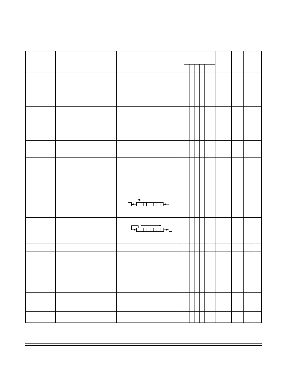
Central Processor Unit (CPU)
Instruction Set Summary
MC68HC908GR16 -- Rev. 1.0
Data Sheet
MOTOROLA
Central Processor Unit (CPU)
95
Table 7-1. Instruction Set Summary (Sheet 1 of 7)
Source
Form
Operation
Description
Effect
on CCR
Addre
s
s
Mod
e
Opc
ode
Ope
r
an
d
Cycl
es
V H I N Z C
ADC #opr
ADC opr
ADC opr
ADC opr,X
ADC opr,X
ADC ,X
ADC opr,SP
ADC opr,SP
Add with Carry
A
(A) + (M) + (C)
�
IMM
DIR
EXT
IX2
IX1
IX
SP1
SP2
A9
B9
C9
D9
E9
F9
9EE9
9ED9
ii
dd
hh ll
ee ff
ff
ff
ee ff
2
3
4
4
3
2
4
5
ADD #opr
ADD opr
ADD opr
ADD opr,X
ADD opr,X
ADD ,X
ADD opr,SP
ADD opr,SP
Add without Carry
A
(A) + (M)
�
IMM
DIR
EXT
IX2
IX1
IX
SP1
SP2
AB
BB
CB
DB
EB
FB
9EEB
9EDB
ii
dd
hh ll
ee ff
ff
ff
ee ff
2
3
4
4
3
2
4
5
AIS #opr
Add Immediate Value (Signed) to SP
SP
(SP) + (16
�
M)
� � � � � � IMM
A7
ii 2
AIX #opr
Add Immediate Value (Signed) to H:X
H:X
(H:X) + (16
�
M)
� � � � � � IMM
AF
ii
2
AND #opr
AND opr
AND opr
AND opr,X
AND opr,X
AND ,X
AND opr,SP
AND opr,SP
Logical AND
A
(A) & (M)
0 � �
�
IMM
DIR
EXT
IX2
IX1
IX
SP1
SP2
A4
B4
C4
D4
E4
F4
9EE4
9ED4
ii
dd
hh ll
ee ff
ff
ff
ee ff
2
3
4
4
3
2
4
5
ASL opr
ASLA
ASLX
ASL opr,X
ASL ,X
ASL opr,SP
Arithmetic Shift Left
(Same as LSL)
� �
DIR
INH
INH
IX1
IX
SP1
38
48
58
68
78
9E68
dd
ff
ff
4
1
1
4
3
5
ASR opr
ASRA
ASRX
ASR opr,X
ASR opr,X
ASR opr,SP
Arithmetic Shift Right
� �
DIR
INH
INH
IX1
IX
SP1
37
47
57
67
77
9E67
dd
ff
ff
4
1
1
4
3
5
BCC rel
Branch if Carry Bit Clear
PC
(PC) + 2 + rel ? (C) = 0
� � � � � � REL
24
rr
3
BCLR n, opr
Clear Bit n in M
Mn
0
� � � � � �
DIR (b0)
DIR (b1)
DIR (b2)
DIR (b3)
DIR (b4)
DIR (b5)
DIR (b6)
DIR (b7)
11
13
15
17
19
1B
1D
1F
dd
dd
dd
dd
dd
dd
dd
dd
4
4
4
4
4
4
4
4
BCS rel
Branch if Carry Bit Set (Same as BLO)
PC
(PC) + 2 + rel ? (C) = 1
� � � � � � REL
25
rr
3
BEQ rel
Branch if Equal
PC
(PC) + 2 + rel ? (Z) = 1
� � � � � � REL
27
rr
3
BGE opr
Branch if Greater Than or Equal To
(Signed Operands)
PC
(PC) + 2 + rel ? (N
V
) = 0
� � � � � � REL
90
rr
3
BGT opr
Branch if Greater Than (Signed
Operands)
PC
(PC) + 2 + rel ? (Z)
| (N
V
) = 0
� � � � � � REL
92
rr
3
C
b0
b7
0
b0
b7
C
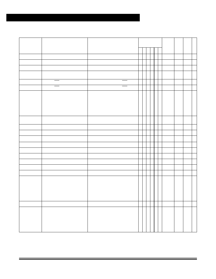
Central Processor Unit (CPU)
Data Sheet
MC68HC908GR16 -- Rev. 1.0
96
Central Processor Unit (CPU)
MOTOROLA
BHCC rel
Branch if Half Carry Bit Clear
PC
(PC) + 2 + rel ? (H) = 0
� � � � � � REL
28
rr
3
BHCS rel
Branch if Half Carry Bit Set
PC
(PC) + 2 + rel ? (H) = 1
� � � � � � REL
29
rr
3
BHI rel
Branch if Higher
PC
(PC) + 2 + rel ? (C) | (Z) = 0
� � � � � � REL
22
rr
3
BHS rel
Branch if Higher or Same
(Same as BCC)
PC
(PC) + 2 + rel ? (C) = 0
� � � � � � REL
24
rr
3
BIH rel
Branch if IRQ Pin High
PC
(PC) + 2 + rel ? IRQ = 1
� � � � � � REL
2F
rr
3
BIL rel
Branch if IRQ Pin Low
PC
(PC) + 2 + rel ? IRQ = 0
� � � � � � REL
2E
rr
3
BIT #opr
BIT opr
BIT opr
BIT opr,X
BIT opr,X
BIT ,X
BIT opr,SP
BIT opr,SP
Bit Test
(A) & (M)
0 � �
�
IMM
DIR
EXT
IX2
IX1
IX
SP1
SP2
A5
B5
C5
D5
E5
F5
9EE5
9ED5
ii
dd
hh ll
ee ff
ff
ff
ee ff
2
3
4
4
3
2
4
5
BLE opr
Branch if Less Than or Equal To
(Signed Operands)
PC
(PC) + 2 + rel ? (Z)
| (N
V
) =
1 � � � � � � REL
93
rr
3
BLO rel
Branch if Lower (Same as BCS)
PC
(PC) + 2 + rel ? (C) = 1
� � � � � � REL
25
rr
3
BLS rel
Branch if Lower or Same
PC
(PC) + 2 + rel ? (C) | (Z) = 1
� � � � � � REL
23
rr
3
BLT opr
Branch if Less Than (Signed Operands)
PC
(PC) + 2 + rel ? (N
V
) =
1
� � � � � � REL
91
rr
3
BMC rel
Branch if Interrupt Mask Clear
PC
(PC) + 2 + rel ? (I) = 0
� � � � � � REL
2C
rr
3
BMI rel
Branch if Minus
PC
(PC) + 2 + rel ? (N) = 1
� � � � � � REL
2B
rr
3
BMS rel
Branch if Interrupt Mask Set
PC
(PC) + 2 + rel ? (I) = 1
� � � � � � REL
2D
rr
3
BNE rel
Branch if Not Equal
PC
(PC) + 2 + rel ? (Z) = 0
� � � � � � REL
26
rr
3
BPL rel
Branch if Plus
PC
(PC) + 2 + rel ? (N) = 0
� � � � � � REL
2A
rr
3
BRA rel
Branch Always
PC
(PC) + 2 + rel � � � � � � REL
20
rr
3
BRCLR n,opr,rel Branch if Bit n in M Clear
PC
(PC) + 3 + rel ? (Mn) = 0
� � � � �
DIR (b0)
DIR (b1)
DIR (b2)
DIR (b3)
DIR (b4)
DIR (b5)
DIR (b6)
DIR (b7)
01
03
05
07
09
0B
0D
0F
dd rr
dd rr
dd rr
dd rr
dd rr
dd rr
dd rr
dd rr
5
5
5
5
5
5
5
5
BRN rel
Branch Never
PC
(PC) + 2
� � � � � � REL
21
rr
3
BRSET n,opr,rel Branch if Bit n in M Set
PC
(PC) + 3 + rel ? (Mn) = 1
� � � � �
DIR (b0)
DIR (b1)
DIR (b2)
DIR (b3)
DIR (b4)
DIR (b5)
DIR (b6)
DIR (b7)
00
02
04
06
08
0A
0C
0E
dd rr
dd rr
dd rr
dd rr
dd rr
dd rr
dd rr
dd rr
5
5
5
5
5
5
5
5
Table 7-1. Instruction Set Summary (Sheet 2 of 7)
Source
Form
Operation
Description
Effect
on CCR
Address
M
ode
Opc
o
de
O
p
er
and
Cy
cl
es
V H I N Z C
Central Processor Unit (CPU)
Instruction Set Summary
MC68HC908GR16 -- Rev. 1.0
Data Sheet
MOTOROLA
Central Processor Unit (CPU)
97
BSET n,opr
Set Bit n in M
Mn
1
� � � � � �
DIR (b0)
DIR (b1)
DIR (b2)
DIR (b3)
DIR (b4)
DIR (b5)
DIR (b6)
DIR (b7)
10
12
14
16
18
1A
1C
1E
dd
dd
dd
dd
dd
dd
dd
dd
4
4
4
4
4
4
4
4
BSR rel
Branch to Subroutine
PC
(PC) + 2; push (PCL)
SP
(SP) � 1; push (PCH)
SP
(SP) � 1
PC
(PC) + rel
� � � � � � REL
AD
rr
4
CBEQ opr,rel
CBEQA #opr,rel
CBEQX #opr,rel
CBEQ opr,X+,rel
CBEQ X+,rel
CBEQ opr,SP,rel
Compare and Branch if Equal
PC
(PC) + 3 + rel ? (A) � (M) = $00
PC
(PC) + 3 + rel ? (A) � (M) = $00
PC
(PC) + 3 + rel ? (X) � (M) = $00
PC
(PC) + 3 + rel ? (A) � (M) = $00
PC
(PC) + 2 + rel ? (A) � (M) = $00
PC
(PC) + 4 + rel ? (A) � (M) = $00
� � � � � �
DIR
IMM
IMM
IX1+
IX+
SP1
31
41
51
61
71
9E61
dd rr
ii rr
ii rr
ff rr
rr
ff rr
5
4
4
5
4
6
CLC
Clear Carry Bit
C
0
� � � � � 0 INH
98
1
CLI
Clear Interrupt Mask
I
0
� � 0 � � � INH
9A
2
CLR opr
CLRA
CLRX
CLRH
CLR opr,X
CLR ,X
CLR opr,SP
Clear
M
$00
A
$00
X
$00
H
$00
M
$00
M
$00
M
$00
0 � � 0 1 �
DIR
INH
INH
INH
IX1
IX
SP1
3F
4F
5F
8C
6F
7F
9E6F
dd
ff
ff
3
1
1
1
3
2
4
CMP #opr
CMP opr
CMP opr
CMP opr,X
CMP opr,X
CMP ,X
CMP opr,SP
CMP opr,SP
Compare A with M
(A) � (M)
� �
IMM
DIR
EXT
IX2
IX1
IX
SP1
SP2
A1
B1
C1
D1
E1
F1
9EE1
9ED1
ii
dd
hh ll
ee ff
ff
ff
ee ff
2
3
4
4
3
2
4
5
COM opr
COMA
COMX
COM opr,X
COM ,X
COM opr,SP
Complement (One's Complement)
M
(M) = $FF � (M)
A
(A) = $FF � (M)
X
(X) = $FF � (M)
M
(M) = $FF � (M)
M
(M) = $FF � (M)
M
(M) = $FF � (M)
0 � �
1
DIR
INH
INH
IX1
IX
SP1
33
43
53
63
73
9E63
dd
ff
ff
4
1
1
4
3
5
CPHX #opr
CPHX opr
Compare H:X with M
(H:X) � (M:M + 1)
� �
IMM
DIR
65
75
ii ii+1
dd
3
4
CPX #opr
CPX opr
CPX opr
CPX ,X
CPX opr,X
CPX opr,X
CPX opr,SP
CPX opr,SP
Compare X with M
(X) � (M)
� �
IMM
DIR
EXT
IX2
IX1
IX
SP1
SP2
A3
B3
C3
D3
E3
F3
9EE3
9ED3
ii
dd
hh ll
ee ff
ff
ff
ee ff
2
3
4
4
3
2
4
5
DAA
Decimal Adjust A
(A)
10
U � �
INH
72
2
Table 7-1. Instruction Set Summary (Sheet 3 of 7)
Source
Form
Operation
Description
Effect
on CCR
Address
M
ode
Opc
o
de
O
p
er
and
Cy
cl
es
V H I N Z C
Central Processor Unit (CPU)
Data Sheet
MC68HC908GR16 -- Rev. 1.0
98
Central Processor Unit (CPU)
MOTOROLA
DBNZ opr,rel
DBNZA rel
DBNZX rel
DBNZ opr,X,rel
DBNZ X,rel
DBNZ opr,SP,rel
Decrement and Branch if Not Zero
A
(A) � 1 or M
(M) � 1 or X
(X) � 1
PC
(PC) + 3 + rel ? (result)
0
PC
(PC) + 2 + rel ? (result)
0
PC
(PC) + 2 + rel ? (result)
0
PC
(PC) + 3 + rel ? (result)
0
PC
(PC) + 2 + rel ? (result)
0
PC
(PC) + 4 + rel ? (result)
0
� � � � � �
DIR
INH
INH
IX1
IX
SP1
3B
4B
5B
6B
7B
9E6B
dd rr
rr
rr
ff rr
rr
ff rr
5
3
3
5
4
6
DEC opr
DECA
DECX
DEC opr,X
DEC ,X
DEC opr,SP
Decrement
M
(M) � 1
A
(A) � 1
X
(X) � 1
M
(M) � 1
M
(M) � 1
M
(M) � 1
� �
�
DIR
INH
INH
IX1
IX
SP1
3A
4A
5A
6A
7A
9E6A
dd
ff
ff
4
1
1
4
3
5
DIV
Divide
A
(H:A)/(X)
H
Remainder
� � � �
INH
52
7
EOR #opr
EOR opr
EOR opr
EOR opr,X
EOR opr,X
EOR ,X
EOR opr,SP
EOR opr,SP
Exclusive OR M with A
A
(A
M)
0 � �
�
IMM
DIR
EXT
IX2
IX1
IX
SP1
SP2
A8
B8
C8
D8
E8
F8
9EE8
9ED8
ii
dd
hh ll
ee ff
ff
ff
ee ff
2
3
4
4
3
2
4
5
INC opr
INCA
INCX
INC opr,X
INC ,X
INC opr,SP
Increment
M
(M) + 1
A
(A) + 1
X
(X) + 1
M
(M) + 1
M
(M) + 1
M
(M) + 1
� �
�
DIR
INH
INH
IX1
IX
SP1
3C
4C
5C
6C
7C
9E6C
dd
ff
ff
4
1
1
4
3
5
JMP opr
JMP opr
JMP opr,X
JMP opr,X
JMP ,X
Jump
PC
Jump Address
� � � � � �
DIR
EXT
IX2
IX1
IX
BC
CC
DC
EC
FC
dd
hh ll
ee ff
ff
2
3
4
3
2
JSR opr
JSR opr
JSR opr,X
JSR opr,X
JSR ,X
Jump to Subroutine
PC
(PC) + n (n = 1, 2, or 3)
Push (PCL); SP
(SP) � 1
Push (PCH); SP
(SP) � 1
PC
Unconditional Address
� � � � � �
DIR
EXT
IX2
IX1
IX
BD
CD
DD
ED
FD
dd
hh ll
ee ff
ff
4
5
6
5
4
LDA #opr
LDA opr
LDA opr
LDA opr,X
LDA opr,X
LDA ,X
LDA opr,SP
LDA opr,SP
Load A from M
A
(M)
0 � �
�
IMM
DIR
EXT
IX2
IX1
IX
SP1
SP2
A6
B6
C6
D6
E6
F6
9EE6
9ED6
ii
dd
hh ll
ee ff
ff
ff
ee ff
2
3
4
4
3
2
4
5
LDHX #opr
LDHX opr
Load H:X from M
H:X
(
M:M
+ 1
)
0 � �
�
IMM
DIR
45
55
ii jj
dd
3
4
LDX #opr
LDX opr
LDX opr
LDX opr,X
LDX opr,X
LDX ,X
LDX opr,SP
LDX opr,SP
Load X from M
X
(M)
0 � �
�
IMM
DIR
EXT
IX2
IX1
IX
SP1
SP2
AE
BE
CE
DE
EE
FE
9EEE
9EDE
ii
dd
hh ll
ee ff
ff
ff
ee ff
2
3
4
4
3
2
4
5
Table 7-1. Instruction Set Summary (Sheet 4 of 7)
Source
Form
Operation
Description
Effect
on CCR
Address
M
ode
Opc
o
de
O
p
er
and
Cy
cl
es
V H I N Z C
Central Processor Unit (CPU)
Instruction Set Summary
MC68HC908GR16 -- Rev. 1.0
Data Sheet
MOTOROLA
Central Processor Unit (CPU)
99
LSL opr
LSLA
LSLX
LSL opr,X
LSL ,X
LSL opr,SP
Logical Shift Left
(Same as ASL)
� �
DIR
INH
INH
IX1
IX
SP1
38
48
58
68
78
9E68
dd
ff
ff
4
1
1
4
3
5
LSR opr
LSRA
LSRX
LSR opr,X
LSR ,X
LSR opr,SP
Logical Shift Right
� � 0
DIR
INH
INH
IX1
IX
SP1
34
44
54
64
74
9E64
dd
ff
ff
4
1
1
4
3
5
MOV opr,opr
MOV opr,X+
MOV #opr,opr
MOV X+,opr
Move
(M)
Destination
(M)
Source
H:X
(H:X) + 1 (IX+D, DIX+)
0 � �
�
DD
DIX+
IMD
IX+D
4E
5E
6E
7E
dd dd
dd
ii dd
dd
5
4
4
4
MUL
Unsigned multiply
X:A
(X)
�
(A)
� 0 � � � 0 INH
42
5
NEG opr
NEGA
NEGX
NEG opr,X
NEG ,X
NEG opr,SP
Negate (Two's Complement)
M
�(M) = $00 � (M)
A
�(A) = $00 � (A)
X
�(X) = $00 � (X)
M
�(M) = $00 � (M)
M
�(M) = $00 � (M)
� �
DIR
INH
INH
IX1
IX
SP1
30
40
50
60
70
9E60
dd
ff
ff
4
1
1
4
3
5
NOP
No Operation
None
� � � � � � INH
9D
1
NSA
Nibble Swap A
A
(A[3:0]:A[7:4])
� � � � � � INH
62
3
ORA #opr
ORA opr
ORA opr
ORA opr,X
ORA opr,X
ORA ,X
ORA opr,SP
ORA opr,SP
Inclusive OR A and M
A
(A) | (M)
0 � �
�
IMM
DIR
EXT
IX2
IX1
IX
SP1
SP2
AA
BA
CA
DA
EA
FA
9EEA
9EDA
ii
dd
hh ll
ee ff
ff
ff
ee ff
2
3
4
4
3
2
4
5
PSHA
Push A onto Stack
Push (A); SP
(SP
) �
1
� � � � � � INH
87
2
PSHH
Push H onto Stack
Push (H)
;
SP
(SP
) �
1 � � � � � � INH
8B
2
PSHX
Push X onto Stack
Push (X)
;
SP
(SP
) �
1 � � � � � � INH
89
2
PULA
Pull A from Stack
SP
(SP +
1); Pull
(
A
)
� � � � � � INH
86
2
PULH
Pull H from Stack
SP
(SP +
1); Pull
(
H
)
� � � � � � INH
8A
2
PULX
Pull X from Stack
SP
(SP +
1); Pull
(
X
)
� � � � � � INH
88
2
ROL opr
ROLA
ROLX
ROL opr,X
ROL ,X
ROL opr,SP
Rotate Left through Carry
� �
DIR
INH
INH
IX1
IX
SP1
39
49
59
69
79
9E69
dd
ff
ff
4
1
1
4
3
5
ROR opr
RORA
RORX
ROR opr,X
ROR ,X
ROR opr,SP
Rotate Right through Carry
� �
DIR
INH
INH
IX1
IX
SP1
36
46
56
66
76
9E66
dd
ff
ff
4
1
1
4
3
5
Table 7-1. Instruction Set Summary (Sheet 5 of 7)
Source
Form
Operation
Description
Effect
on CCR
Address
M
ode
Opc
o
de
O
p
er
and
Cy
cl
es
V H I N Z C
C
b0
b7
0
b0
b7
C
0
C
b0
b7
b0
b7
C
Central Processor Unit (CPU)
Data Sheet
MC68HC908GR16 -- Rev. 1.0
100
Central Processor Unit (CPU)
MOTOROLA
RSP
Reset Stack Pointer
SP
$FF
� � � � � � INH
9C
1
RTI
Return from Interrupt
SP
(SP) + 1; Pull (CCR)
SP
(SP) + 1; Pull (A)
SP
(SP) + 1; Pull (X)
SP
(SP) + 1; Pull (PCH)
SP
(SP) + 1; Pull (PCL)
INH
80
7
RTS
Return from Subroutine
SP
SP + 1
;
Pull
(
PCH)
SP
SP + 1; Pull (PCL)
� � � � � � INH
81
4
SBC #opr
SBC opr
SBC opr
SBC opr,X
SBC opr,X
SBC ,X
SBC opr,SP
SBC opr,SP
Subtract with Carry
A
(A) � (M) � (C)
� �
IMM
DIR
EXT
IX2
IX1
IX
SP1
SP2
A2
B2
C2
D2
E2
F2
9EE2
9ED2
ii
dd
hh ll
ee ff
ff
ff
ee ff
2
3
4
4
3
2
4
5
SEC
Set Carry Bit
C
1
� � � � � 1 INH
99
1
SEI
Set Interrupt Mask
I
1
� � 1 � � � INH
9B
2
STA opr
STA opr
STA opr,X
STA opr,X
STA ,X
STA opr,SP
STA opr,SP
Store A in M
M
(A)
0 � �
�
DIR
EXT
IX2
IX1
IX
SP1
SP2
B7
C7
D7
E7
F7
9EE7
9ED7
dd
hh ll
ee ff
ff
ff
ee ff
3
4
4
3
2
4
5
STHX opr
Store H:X in M
(M:M + 1)
(H:X)
0 � �
� DIR
35
dd
4
STOP
Enable IRQ Pin; Stop Oscillator
I
0; Stop Oscillator
� � 0 � � � INH
8E
1
STX opr
STX opr
STX opr,X
STX opr,X
STX ,X
STX opr,SP
STX opr,SP
Store X in M
M
(X)
0 � �
�
DIR
EXT
IX2
IX1
IX
SP1
SP2
BF
CF
DF
EF
FF
9EEF
9EDF
dd
hh ll
ee ff
ff
ff
ee ff
3
4
4
3
2
4
5
SUB #opr
SUB opr
SUB opr
SUB opr,X
SUB opr,X
SUB ,X
SUB opr,SP
SUB opr,SP
Subtract A
(A)
�
(M)
� �
IMM
DIR
EXT
IX2
IX1
IX
SP1
SP2
A0
B0
C0
D0
E0
F0
9EE0
9ED0
ii
dd
hh ll
ee ff
ff
ff
ee ff
2
3
4
4
3
2
4
5
SWI
Software Interrupt
PC
(PC) + 1; Push (PCL)
SP
(SP) � 1; Push (PCH)
SP
(SP) � 1; Push (X)
SP
(SP) � 1; Push (A)
SP
(SP) � 1; Push (CCR)
SP
(SP) � 1; I
1
PCH
Interrupt Vector High Byte
PCL
Interrupt Vector Low Byte
� � 1 � � � INH
83
9
TAP
Transfer A to CCR
CCR
(A)
INH
84
2
TAX
Transfer A to X
X
(A)
� � � � � � INH
97
1
TPA
Transfer CCR to A
A
(CCR)
� � � � � � INH
85
1
Table 7-1. Instruction Set Summary (Sheet 6 of 7)
Source
Form
Operation
Description
Effect
on CCR
Address
M
ode
Opc
o
de
O
p
er
and
Cy
cl
es
V H I N Z C
Central Processor Unit (CPU)
Opcode Map
MC68HC908GR16 -- Rev. 1.0
Data Sheet
MOTOROLA
Central Processor Unit (CPU)
101
7.8 Opcode Map
See
Table 7-2
.
TST opr
TSTA
TSTX
TST opr,X
TST ,X
TST opr,SP
Test for Negative or Zero
(A) � $00 or (X) � $00 or (M) � $00
0 � �
�
DIR
INH
INH
IX1
IX
SP1
3D
4D
5D
6D
7D
9E6D
dd
ff
ff
3
1
1
3
2
4
TSX
Transfer SP to H:X
H:X
(SP) + 1
� � � � � � INH
95
2
TXA
Transfer X to A
A
(X)
� � � � � � INH
9F
1
TXS
Transfer H:X to SP
(SP)
(H:X) � 1
� � � � � � INH
94
2
A
Accumulator
n
Any bit
C
Carry/borrow bit
opr
Operand (one or two bytes)
CCR
Condition code register
PC
Program counter
dd
Direct address of operand
PCH Program counter high byte
dd rr
Direct address of operand and relative offset of branch instruction
PCL Program counter low byte
DD
Direct to direct addressing mode
REL Relative addressing mode
DIR
Direct addressing mode
rel
Relative program counter offset byte
DIX+
Direct to indexed with post increment addressing mode
rr
Relative program counter offset byte
ee ff
High and low bytes of offset in indexed, 16-bit offset addressing
SP1 Stack pointer, 8-bit offset addressing mode
EXT
Extended addressing mode
SP2 Stack pointer 16-bit offset addressing mode
ff
Offset byte in indexed, 8-bit offset addressing
SP
Stack pointer
H
Half-carry bit
U
Undefined
H
Index register high byte
V
Overflow bit
hh ll
High and low bytes of operand address in extended addressing
X
Index register low byte
I
Interrupt mask
Z
Zero bit
ii
Immediate operand byte
&
Logical AND
IMD
Immediate source to direct destination addressing mode
|
Logical OR
IMM
Immediate addressing mode
Logical EXCLUSIVE OR
INH
Inherent addressing mode
( )
Contents of
IX
Indexed, no offset addressing mode
�( )
Negation (two's complement)
IX+
Indexed, no offset, post increment addressing mode
#
Immediate value
IX+D
Indexed with post increment to direct addressing mode
�
Sign extend
IX1
Indexed, 8-bit offset addressing mode
Loaded with
IX1+
Indexed, 8-bit offset, post increment addressing mode
?
If
IX2
Indexed, 16-bit offset addressing mode
:
Concatenated with
M
Memory location
Set or cleared
N
Negative bit
--
Not affected
Table 7-1. Instruction Set Summary (Sheet 7 of 7)
Source
Form
Operation
Description
Effect
on CCR
Address
M
ode
Opc
o
de
O
p
er
and
Cy
cl
es
V H I N Z C
Data Sheet
MC6
8
HC90
8
GR16 --
Re
v. 1.0
102
Cen
t
ral
Proce
s
so
r Un
it (CPU)
M
OTOROLA
Central Pr
ocessor Unit (CPU)
Table 7-2. Opcode Map
Bit Manipulation
Branch
Read-Modify-Write
Control
Register/Memory
DIR
DIR
REL
DIR
INH
INH
IX1
SP1
IX
INH
INH
IMM
DIR
EXT
IX2
SP2
IX1
SP1
IX
0
1
2
3
4
5
6
9E6
7
8
9
A
B
C
D
9ED
E
9EE
F
0
5
BRSET0
3
DIR
4
BSET0
2
DIR
3
BRA
2
REL
4
NEG
2
DIR
1
NEGA
1
INH
1
NEGX
1
INH
4
NEG
2
IX1
5
NEG
3
SP1
3
NEG
1
IX
7
RTI
1
INH
3
BGE
2
REL
2
SUB
2
IMM
3
SUB
2
DIR
4
SUB
3
EXT
4
SUB
3
IX2
5
SUB
4
SP2
3
SUB
2
IX1
4
SUB
3
SP1
2
SUB
1
IX
1
5
BRCLR0
3
DIR
4
BCLR0
2
DIR
3
BRN
2
REL
5
CBEQ
3
DIR
4
CBEQA
3
IMM
4
CBEQX
3
IMM
5
CBEQ
3 IX1+
6
CBEQ
4
SP1
4
CBEQ
2
IX+
4
RTS
1
INH
3
BLT
2
REL
2
CMP
2
IMM
3
CMP
2
DIR
4
CMP
3
EXT
4
CMP
3
IX2
5
CMP
4
SP2
3
CMP
2
IX1
4
CMP
3
SP1
2
CMP
1
IX
2
5
BRSET1
3
DIR
4
BSET1
2
DIR
3
BHI
2
REL
5
MUL
1
INH
7
DIV
1
INH
3
NSA
1
INH
2
DAA
1
INH
3
BGT
2
REL
2
SBC
2
IMM
3
SBC
2
DIR
4
SBC
3
EXT
4
SBC
3
IX2
5
SBC
4
SP2
3
SBC
2
IX1
4
SBC
3
SP1
2
SBC
1
IX
3
5
BRCLR1
3
DIR
4
BCLR1
2
DIR
3
BLS
2
REL
4
COM
2
DIR
1
COMA
1
INH
1
COMX
1
INH
4
COM
2
IX1
5
COM
3
SP1
3
COM
1
IX
9
SWI
1
INH
3
BLE
2
REL
2
CPX
2
IMM
3
CPX
2
DIR
4
CPX
3
EXT
4
CPX
3
IX2
5
CPX
4
SP2
3
CPX
2
IX1
4
CPX
3
SP1
2
CPX
1
IX
4
5
BRSET2
3
DIR
4
BSET2
2
DIR
3
BCC
2
REL
4
LSR
2
DIR
1
LSRA
1
INH
1
LSRX
1
INH
4
LSR
2
IX1
5
LSR
3
SP1
3
LSR
1
IX
2
TAP
1
INH
2
TXS
1
INH
2
AND
2
IMM
3
AND
2
DIR
4
AND
3
EXT
4
AND
3
IX2
5
AND
4
SP2
3
AND
2
IX1
4
AND
3
SP1
2
AND
1
IX
5
5
BRCLR2
3
DIR
4
BCLR2
2
DIR
3
BCS
2
REL
4
STHX
2
DIR
3
LDHX
3
IMM
4
LDHX
2
DIR
3
CPHX
3
IMM
4
CPHX
2
DIR
1
TPA
1
INH
2
TSX
1
INH
2
BIT
2
IMM
3
BIT
2
DIR
4
BIT
3
EXT
4
BIT
3
IX2
5
BIT
4
SP2
3
BIT
2
IX1
4
BIT
3
SP1
2
BIT
1
IX
6
5
BRSET3
3
DIR
4
BSET3
2
DIR
3
BNE
2
REL
4
ROR
2
DIR
1
RORA
1
INH
1
RORX
1
INH
4
ROR
2
IX1
5
ROR
3
SP1
3
ROR
1
IX
2
PULA
1
INH
2
LDA
2
IMM
3
LDA
2
DIR
4
LDA
3
EXT
4
LDA
3
IX2
5
LDA
4
SP2
3
LDA
2
IX1
4
LDA
3
SP1
2
LDA
1
IX
7
5
BRCLR3
3
DIR
4
BCLR3
2
DIR
3
BEQ
2
REL
4
ASR
2
DIR
1
ASRA
1
INH
1
ASRX
1
INH
4
ASR
2
IX1
5
ASR
3
SP1
3
ASR
1
IX
2
PSHA
1
INH
1
TAX
1
INH
2
AIS
2
IMM
3
STA
2
DIR
4
STA
3
EXT
4
STA
3
IX2
5
STA
4
SP2
3
STA
2
IX1
4
STA
3
SP1
2
STA
1
IX
8
5
BRSET4
3
DIR
4
BSET4
2
DIR
3
BHCC
2
REL
4
LSL
2
DIR
1
LSLA
1
INH
1
LSLX
1
INH
4
LSL
2
IX1
5
LSL
3
SP1
3
LSL
1
IX
2
PULX
1
INH
1
CLC
1
INH
2
EOR
2
IMM
3
EOR
2
DIR
4
EOR
3
EXT
4
EOR
3
IX2
5
EOR
4
SP2
3
EOR
2
IX1
4
EOR
3
SP1
2
EOR
1
IX
9
5
BRCLR4
3
DIR
4
BCLR4
2
DIR
3
BHCS
2
REL
4
ROL
2
DIR
1
ROLA
1
INH
1
ROLX
1
INH
4
ROL
2
IX1
5
ROL
3
SP1
3
ROL
1
IX
2
PSHX
1
INH
1
SEC
1
INH
2
ADC
2
IMM
3
ADC
2
DIR
4
ADC
3
EXT
4
ADC
3
IX2
5
ADC
4
SP2
3
ADC
2
IX1
4
ADC
3
SP1
2
ADC
1
IX
A
5
BRSET5
3
DIR
4
BSET5
2
DIR
3
BPL
2
REL
4
DEC
2
DIR
1
DECA
1
INH
1
DECX
1
INH
4
DEC
2
IX1
5
DEC
3
SP1
3
DEC
1
IX
2
PULH
1
INH
2
CLI
1
INH
2
ORA
2
IMM
3
ORA
2
DIR
4
ORA
3
EXT
4
ORA
3
IX2
5
ORA
4
SP2
3
ORA
2
IX1
4
ORA
3
SP1
2
ORA
1
IX
B
5
BRCLR5
3
DIR
4
BCLR5
2
DIR
3
BMI
2
REL
5
DBNZ
3
DIR
3
DBNZA
2
INH
3
DBNZX
2
INH
5
DBNZ
3
IX1
6
DBNZ
4
SP1
4
DBNZ
2
IX
2
PSHH
1
INH
2
SEI
1
INH
2
ADD
2
IMM
3
ADD
2
DIR
4
ADD
3
EXT
4
ADD
3
IX2
5
ADD
4
SP2
3
ADD
2
IX1
4
ADD
3
SP1
2
ADD
1
IX
C
5
BRSET6
3
DIR
4
BSET6
2
DIR
3
BMC
2
REL
4
INC
2
DIR
1
INCA
1
INH
1
INCX
1
INH
4
INC
2
IX1
5
INC
3
SP1
3
INC
1
IX
1
CLRH
1
INH
1
RSP
1
INH
2
JMP
2
DIR
3
JMP
3
EXT
4
JMP
3
IX2
3
JMP
2
IX1
2
JMP
1
IX
D
5
BRCLR6
3
DIR
4
BCLR6
2
DIR
3
BMS
2
REL
3
TST
2
DIR
1
TSTA
1
INH
1
TSTX
1
INH
3
TST
2
IX1
4
TST
3
SP1
2
TST
1
IX
1
NOP
1
INH
4
BSR
2
REL
4
JSR
2
DIR
5
JSR
3
EXT
6
JSR
3
IX2
5
JSR
2
IX1
4
JSR
1
IX
E
5
BRSET7
3
DIR
4
BSET7
2
DIR
3
BIL
2
REL
5
MOV
3
DD
4
MOV
2 DIX+
4
MOV
3
IMD
4
MOV
2 IX+D
1
STOP
1
INH
*
2
LDX
2
IMM
3
LDX
2
DIR
4
LDX
3
EXT
4
LDX
3
IX2
5
LDX
4
SP2
3
LDX
2
IX1
4
LDX
3
SP1
2
LDX
1
IX
F
5
BRCLR7
3
DIR
4
BCLR7
2
DIR
3
BIH
2
REL
3
CLR
2
DIR
1
CLRA
1
INH
1
CLRX
1
INH
3
CLR
2
IX1
4
CLR
3
SP1
2
CLR
1
IX
1
WAIT
1
INH
1
TXA
1
INH
2
AIX
2
IMM
3
STX
2
DIR
4
STX
3
EXT
4
STX
3
IX2
5
STX
4
SP2
3
STX
2
IX1
4
STX
3
SP1
2
STX
1
IX
INH Inherent
REL Relative
SP1 Stack Pointer, 8-Bit Offset
IMM Immediate
IX
Indexed, No Offset
SP2 Stack Pointer, 16-Bit Offset
DIR Direct
IX1
Indexed, 8-Bit Offset
IX+
Indexed, No Offset with
EXT Extended
IX2
Indexed, 16-Bit Offset
Post Increment
DD
Direct-Direct
IMD Immediate-Direct
IX1+ Indexed, 1-Byte Offset with
IX+D Indexed-Direct
DIX+ Direct-Indexed
Post Increment
*
Pre-byte for stack pointer indexed instructions
0
High Byte of Opcode in Hexadecimal
Low Byte of Opcode in Hexadecimal
0
5
BRSET0
3
DIR
Cycles
Opcode Mnemonic
Number of Bytes / Addressing Mode
MSB
LSB
MSB
LSB

MC68HC908GR16 -- Rev. 1.0
Data Sheet
MOTOROLA
External Interrupt (IRQ)
103
Data Sheet -- MC68HC908GR16
Section 8. External Interrupt (IRQ)
8.1 Introduction
The IRQ (external interrupt) module provides a maskable interrupt input.
8.2 Features
Features of the IRQ module include:
�
A dedicated external interrupt pin (IRQ)
�
IRQ interrupt control bits
�
Hysteresis buffer
�
Programmable edge-only or edge and level interrupt sensitivity
�
Automatic interrupt acknowledge
�
Internal pullup resistor
8.3 Functional Description
A logic 0 applied to the external interrupt pin can latch a central processor unit
(CPU) interrupt request.
Figure 8-2
shows the structure of the IRQ module.
Interrupt signals on the IRQ pin are latched into the IRQ latch. An interrupt latch
remains set until one of the following actions occurs:
�
Vector fetch -- A vector fetch automatically generates an interrupt
acknowledge signal that clears the latch that caused the vector fetch.
�
Software clear -- Software can clear an interrupt latch by writing to the
appropriate acknowledge bit in the interrupt status and control register
(INTSCR). Writing a logic 1 to the ACK bit clears the IRQ latch.
�
Reset -- A reset automatically clears the interrupt latch.
The external interrupt pin is falling-edge triggered and is software-configurable to
be either falling-edge or falling-edge and low-level triggered. The MODE bit in the
INTSCR controls the triggering sensitivity of the IRQ pin.
When an interrupt pin is edge-triggered only, the interrupt remains set until a vector
fetch, software clear, or reset occurs.
Data Sheet
MC6
8
HC90
8
GR16 --
Re
v. 1.0
104
Ext
e
rn
al In
te
rru
p
t
(I
RQ)
M
OT
ORO
L
A
External Interrupt (IRQ)
Figure 8-1. Block Diagram Highlighting IRQ Block and Pins
MONITOR MODULE
M68HC08 CPU
CONTROL AND STATUS REGISTERS -- 64 BYTES
USER FLASH -- 15,872 BYTES
USER RAM -- 1024 BYTES
MONITOR ROM -- 350 BYTES
USER FLASH VECTOR SPACE -- 44 BYTES
PORTA
D
DRA
DDRC
PO
R
T
C
DDR
D
PORTD
DDRE
POR
T
E
INTERNAL BUS
OSC1
OSC2
RST
(3)
IRQ
(3)
PTA7/KBD7�PTA0/KBD0
(1)
PTB7/AD7
PTB6/AD6
PTB5/AD5
PTB4/AD4
PTB3/AD3
PTB2/AD2
PTB1/AD1
PTB0/AD0
PTC6
(1)
PTC5
(1)
PTC4
(1), (2)
PTC3
(1), (2)
PTC2
(1), (2)
PTC1
(1), (2)
PTC0
(1), (2)
PTD7/T2CH1
(1)
PTD6/T2CH0
(1)
PTD5/T1CH1
(1)
PTD4/T1CH0
(1)
PTD3/SPSCK
(1)
PTD2/MOSI
(1)
PTD1/MISO
(1)
PTD0/SS
(1)
PTE1/RxD
PTE0/TxD
SECURITY
MODULE
POWER
V
SS
V
DD
V
SSA
V
DDA
1. Ports are software configurable with pullup device if input port.
2. Higher current drive port pins
3. Pin contains integrated pullup device
MONITOR MODE ENTRY
MODULE
DDRB
PORTB
V
DDAD
/V
REFH
V
DDAD
/V
REFL
PTE5�PTE2
FLASH PROGRAMMING ROUTINES ROM -- 406 BYTES
CLOCK GENERATOR MODULE
CGMXFC
PHASE LOCKED LOOP
32�100 kHz OSCILLATOR
CPU
REGISTERS
ARITHMETIC/LOGIC
UNIT (ALU)
SYSTEM INTEGRATION
MODULE
SINGLE EXTERNAL
INTERRUPT MODULE
10-BIT ANALOG-TO-DIGITAL
CONVERTER MODULE
POWER-ON RESET
MODULE
PROGRAMMABLE TIMEBASE
MODULE
SINGLE BREAKPOINT
BREAK MODULE
DUAL VOLTAGE
LOW-VOLTAGE INHIBIT
MODULE
8-BIT KEYBOARD
INTERRUPT MODULE
2-CHANNEL TIMER
INTERFACE MODULE 1
2-CHANNEL TIMER
INTERFACE MODULE 2
ENHANCED SERIAL
COMUNICATIONS
INTERFACE MODULE
COMPUTER OPERATING
PROPERLY MODULE
SERIAL PERIPHERAL
INTERFACE MODULE
DATA BUS SWITCH
MODULE
MEMORY MAP
MODULE
CONFIGURATION
REGISTER 1�2
MODULE
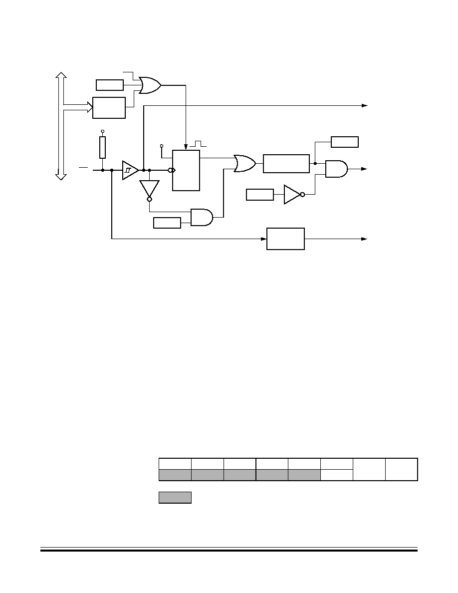
External Interrupt (IRQ)
Functional Description
MC68HC908GR16 -- Rev. 1.0
Data Sheet
MOTOROLA
External Interrupt (IRQ)
105
Figure 8-2. IRQ Module Block Diagram
When an interrupt pin is both falling-edge and low-level triggered, the interrupt
remains set until both of these events occur:
�
Vector fetch or software clear
�
Return of the interrupt pin to logic 1
The vector fetch or software clear may occur before or after the interrupt pin returns
to logic 1. As long as the pin is low, the interrupt request remains pending. A reset
will clear the latch and the MODE control bit, thereby clearing the interrupt even if
the pin stays low.
When set, the IMASK bit in the INTSCR mask all external interrupt requests. A
latched interrupt request is not presented to the interrupt priority logic unless the
IMASK bit is clear.
NOTE:
The interrupt mask (I) in the condition code register (CCR) masks all interrupt
requests, including external interrupt requests.
IMASK
D
Q
CK
CLR
IRQ
HIGH
INTERRUPT
TO MODE
SELECT
LOGIC
REQUEST
V
DD
MODE
VOLTAGE
DETECT
IRQF
TO CPU FOR
BIL/BIH
INSTRUCTIONS
VECTOR
FETCH
DECODER
INTERNA
L A
DDRESS
BUS
RESET
V
DD
INTERNAL
PULLUP
DEVICE
ACK
IRQ
SYNCHRONIZER
Addr.
Register Name
Bit 7
6
5
4
3
2
1
Bit 0
$001D
IRQ Status and Control
Register (INTSCR)
See page 107.
Read:
0
0
0
0
IRQF
0
IMASK
MODE
Write:
ACK
Reset:
0
0
0
0
0
0
0
0
= Unimplemented
Figure 8-3. IRQ I/O Register Summary

External Interrupt (IRQ)
Data Sheet
MC68HC908GR16 -- Rev. 1.0
106
External Interrupt (IRQ)
MOTOROLA
8.4 IRQ Pin
A logic 0 on the IRQ pin can latch an interrupt request into the IRQ latch. A vector
fetch, software clear, or reset clears the IRQ latch.
If the MODE bit is set, the IRQ pin is both falling-edge-sensitive and
low-level-sensitive. With MODE set, both of the following actions must occur to
clear IRQ:
�
Vector fetch or software clear -- A vector fetch generates an interrupt
acknowledge signal to clear the latch. Software may generate the interrupt
acknowledge signal by writing a logic 1 to the ACK bit in the interrupt status
and control register (INTSCR). The ACK bit is useful in applications that poll
the IRQ pin and require software to clear the IRQ latch. Writing to the ACK
bit prior to leaving an interrupt service routine can also prevent spurious
interrupts due to noise. Setting ACK does not affect subsequent transitions
on the IRQ pin. A falling edge that occurs after writing to the ACK bit another
interrupt request. If the IRQ mask bit, IMASK, is clear, the CPU loads the
program counter with the vector address at locations $FFFA and $FFFB.
�
Return of the IRQ pin to logic 1 -- As long as the IRQ pin is at logic 0, IRQ
remains active.
The vector fetch or software clear and the return of the IRQ pin to logic 1 may occur
in any order. The interrupt request remains pending as long as the IRQ pin is at
logic 0. A reset will clear the latch and the MODE control bit, thereby clearing the
interrupt even if the pin stays low.
If the MODE bit is clear, the IRQ pin is falling-edge-sensitive only. With MODE
clear, a vector fetch or software clear immediately clears the IRQ latch.
The IRQF bit in the INTSCR register can be used to check for pending interrupts.
The IRQF bit is not affected by the IMASK bit, which makes it useful in applications
where polling is preferred.
Use the BIH or BIL instruction to read the logic level on the IRQ pin.
NOTE:
When using the level-sensitive interrupt trigger, avoid false interrupts by masking
interrupt requests in the interrupt routine.
8.5 IRQ Module During Break Interrupts
The BCFE bit in the SIM break flag control register (SBFCR) enables software to
clear the latch during the break state. See
Section 19. Development Support
.
To allow software to clear the IRQ latch during a break interrupt, write a logic 1 to
the BCFE bit. If a latch is cleared during the break state, it remains cleared when
the MCU exits the break state.

External Interrupt (IRQ)
IRQ Status and Control Register
MC68HC908GR16 -- Rev. 1.0
Data Sheet
MOTOROLA
External Interrupt (IRQ)
107
To protect CPU interrupt flags during the break state, write a logic 0 to the BCFE
bit. With BCFE at logic 0 (its default state), writing to the ACK bit in the IRQ status
and control register during the break state has no effect on the IRQ interrupt flags.
8.6 IRQ Status and Control Register
The IRQ status and control register (INTSCR) controls and monitors operation of
the IRQ module. The INTSCR:
�
Shows the state of the IRQ flag
�
Clears the IRQ latch
�
Masks IRQ interrupt request
�
Controls triggering sensitivity of the IRQ interrupt pin.
IRQF -- IRQ Flag Bit
This read-only status bit is high when the IRQ interrupt is pending.
1 = IRQ interrupt pending
0 = IRQ interrupt not pending
ACK -- IRQ Interrupt Request Acknowledge Bit
Writing a logic 1 to this write-only bit clears the IRQ latch. ACK always reads as
logic 0. Reset clears ACK.
IMASK -- IRQ Interrupt Mask Bit
Writing a logic 1 to this read/write bit disables IRQ interrupt requests. Reset
clears IMASK.
1 = IRQ interrupt requests disabled
0 = IRQ interrupt requests enabled
MODE -- IRQ Edge/Level Select Bit
This read/write bit controls the triggering sensitivity of the IRQ pin. Reset clears
MODE.
1 = IRQ interrupt requests on falling edges and low levels
0 = IRQ interrupt requests on falling edges only
Address:
$001D
Bit 7
6
5
4
3
2
1
Bit 0
Read:
IRQF
0
IMASK
MODE
Write:
ACK
Reset:
0
0
0
0
0
0
0
0
= Unimplemented
Figure 8-4. IRQ Status and Control Register (INTSCR)

External Interrupt (IRQ)
Data Sheet
MC68HC908GR16 -- Rev. 1.0
108
External Interrupt (IRQ)
MOTOROLA

MC68HC908GR16 -- Rev. 1.0
Data Sheet
MOTOROLA
Keyboard Interrupt Module (KBI)
109
Data Sheet -- MC68HC908GR16
Section 9. Keyboard Interrupt Module (KBI)
9.1 Introduction
The keyboard interrupt module (KBI) provides eight independently maskable
external interrupts which are accessible via PTA0�PTA7. When a port pin is
enabled for keyboard interrupt function, an internal pullup device is also enabled
on the pin.
9.2 Features
Features include:
�
Eight keyboard interrupt pins with separate keyboard interrupt enable bits
and one keyboard interrupt mask
�
Hysteresis buffers
�
Programmable edge-only or edge- and level- interrupt sensitivity
�
Exit from low-power modes
�
I/O (input/output) port bit(s) software configurable with pullup device(s) if
configured as input port bit(s)
9.3 Functional Description
Writing to the KBIE7�KBIE0 bits in the keyboard interrupt enable register
independently enables or disables each port A pin as a keyboard interrupt pin.
Enabling a keyboard interrupt pin also enables its internal pullup device. A logic 0
applied to an enabled keyboard interrupt pin latches a keyboard interrupt request.
A keyboard interrupt is latched when one or more keyboard pins goes low after all
were high. The MODEK bit in the keyboard status and control register controls the
triggering mode of the keyboard interrupt.
�
If the keyboard interrupt is edge-sensitive only, a falling edge on a keyboard
pin does not latch an interrupt request if another keyboard pin is already low.
To prevent losing an interrupt request on one pin because another pin is still
low, software can disable the latter pin while it is low.
�
If the keyboard interrupt is falling edge- and low-level sensitive, an interrupt
request is present as long as any keyboard interrupt pin is low and the pin
is keyboard interrupt enabled.

Data Sheet
MC6
8
HC90
8
GR16 --
Re
v. 1.0
110
Keybo
a
rd In
terru
pt Modu
le (KBI)
M
OTOROLA
K
e
yboar
d Interrup
t Modu
le (K
BI)
Figure 9-1. Block Diagram Highlighting KBI Block and Pins
MONITOR MODULE
M68HC08 CPU
CONTROL AND STATUS REGISTERS -- 64 BYTES
USER FLASH -- 15,872 BYTES
USER RAM -- 1024 BYTES
MONITOR ROM -- 350 BYTES
USER FLASH VECTOR SPACE -- 44 BYTES
PORTA
D
DRA
DDRC
PO
R
T
C
DDR
D
PORTD
DDRE
POR
T
E
INTERNAL BUS
OSC1
OSC2
RST
(3)
IRQ
(3)
PTA7/KBD7�PTA0/KBD0
(1)
PTB7/AD7
PTB6/AD6
PTB5/AD5
PTB4/AD4
PTB3/AD3
PTB2/AD2
PTB1/AD1
PTB0/AD0
PTC6
(1)
PTC5
(1)
PTC4
(1), (2)
PTC3
(1), (2)
PTC2
(1), (2)
PTC1
(1), (2)
PTC0
(1), (2)
PTD7/T2CH1
(1)
PTD6/T2CH0
(1)
PTD5/T1CH1
(1)
PTD4/T1CH0
(1)
PTD3/SPSCK
(1)
PTD2/MOSI
(1)
PTD1/MISO
(1)
PTD0/SS
(1)
PTE1/RxD
PTE0/TxD
SECURITY
MODULE
POWER
V
SS
V
DD
V
SSA
V
DDA
1. Ports are software configurable with pullup device if input port.
2. Higher current drive port pins
3. Pin contains integrated pullup device
MONITOR MODE ENTRY
MODULE
DDRB
PORTB
V
DDAD
/V
REFH
V
DDAD
/V
REFL
PTE5�PTE2
FLASH PROGRAMMING ROUTINES ROM -- 406 BYTES
CLOCK GENERATOR MODULE
CGMXFC
PHASE LOCKED LOOP
32�100 kHz OSCILLATOR
CPU
REGISTERS
ARITHMETIC/LOGIC
UNIT (ALU)
SYSTEM INTEGRATION
MODULE
SINGLE EXTERNAL
INTERRUPT MODULE
10-BIT ANALOG-TO-DIGITAL
CONVERTER MODULE
POWER-ON RESET
MODULE
PROGRAMMABLE TIMEBASE
MODULE
SINGLE BREAKPOINT
BREAK MODULE
DUAL VOLTAGE
LOW-VOLTAGE INHIBIT
MODULE
8-BIT KEYBOARD
INTERRUPT MODULE
2-CHANNEL TIMER
INTERFACE MODULE 1
2-CHANNEL TIMER
INTERFACE MODULE 2
ENHANCED SERIAL
COMUNICATIONS
INTERFACE MODULE
COMPUTER OPERATING
PROPERLY MODULE
SERIAL PERIPHERAL
INTERFACE MODULE
DATA BUS SWITCH
MODULE
MEMORY MAP
MODULE
CONFIGURATION
REGISTER 1�2
MODULE

Keyboard Interrupt Module (KBI)
Functional Description
MC68HC908GR16 -- Rev. 1.0
Data Sheet
MOTOROLA
Keyboard Interrupt Module (KBI)
111
Figure 9-2. Keyboard Module Block Diagram
If the MODEK bit is set, the keyboard interrupt pins are both falling edge- and
low-level sensitive, and both of the following actions must occur to clear a keyboard
interrupt request:
�
Vector fetch or software clear -- A vector fetch generates an interrupt
acknowledge signal to clear the interrupt request. Software may generate
the interrupt acknowledge signal by writing a logic 1 to the ACKK bit in the
keyboard status and control register (INTKBSCR). The ACKK bit is useful in
applications that poll the keyboard interrupt pins and require software to
clear the keyboard interrupt request. Writing to the ACKK bit prior to leaving
an interrupt service routine can also prevent spurious interrupts due to
noise. Setting ACKK does not affect subsequent transitions on the keyboard
interrupt pins. A falling edge that occurs after writing to the ACKK bit latches
KB0IE
KB7IE
.
.
.
KEYBOARD
INTERRUPT
D
Q
CK
CLR
V
DD
MODEK
IMASKK
REQUEST
VECTOR FETCH
DECODER
ACKK
INTERNAL BUS
RESET
TO PULLUP ENABLE
KBD7
KBD0
TO PULLUP ENABLE
SYNCHRONIZER
KEYF
Addr.
Register Name
Bit 7
6
5
4
3
2
1
Bit 0
$001A
Keyboard Status
and Control Register
(INTKBSCR)
See page 114.
Read:
0
0
0
0
KEYF
0
IMASKK
MODEK
Write:
ACKK
Reset:
0
0
0
0
0
0
0
0
$001B
Keyboard Interrupt Enable
Register
(INTKBIER)
See page 115.
Read:
KBIE7
KBIE6
KBIE5
KBIE4
KBIE3
KBIE2
KBIE1
KBIE0
Write:
Reset:
0
0
0
0
0
0
0
0
= Unimplemented
Figure 9-3. I/O Register Summary

Keyboard Interrupt Module (KBI)
Data Sheet
MC68HC908GR16 -- Rev. 1.0
112
Keyboard Interrupt Module (KBI)
MOTOROLA
another interrupt request. If the keyboard interrupt mask bit, IMASKK, is
clear, the CPU loads the program counter with the vector address at
locations $FFE0 and $FFE1.
�
Return of all enabled keyboard interrupt pins to logic 1 -- As long as any
enabled keyboard interrupt pin is at logic 0, the keyboard interrupt remains
set.
The vector fetch or software clear and the return of all enabled keyboard interrupt
pins to logic 1 may occur in any order.
If the MODEK bit is clear, the keyboard interrupt pin is falling-edge-sensitive only.
With MODEK clear, a vector fetch or software clear immediately clears the
keyboard interrupt request.
Reset clears the keyboard interrupt request and the MODEK bit, clearing the
interrupt request even if a keyboard interrupt pin stays at logic 0.
The keyboard flag bit (KEYF) in the keyboard status and control register can be
used to see if a pending interrupt exists. The KEYF bit is not affected by the
keyboard interrupt mask bit (IMASKK) which makes it useful in applications where
polling is preferred.
To determine the logic level on a keyboard interrupt pin, use the data direction
register to configure the pin as an input and read the data register.
NOTE:
Setting a keyboard interrupt enable bit (KBIEx) forces the corresponding keyboard
interrupt pin to be an input, overriding the data direction register. However, the data
direction register bit must be a logic 0 for software to read the pin.
9.4 Keyboard Initialization
When a keyboard interrupt pin is enabled, it takes time for the internal pullup to
reach a logic 1. Therefore, a false interrupt can occur as soon as the pin is enabled.
To prevent a false interrupt on keyboard initialization:
1.
Mask keyboard interrupts by setting the IMASKK bit in the keyboard status
and control register.
2.
Enable the KBI pins by setting the appropriate KBIEx bits in the keyboard
interrupt enable register.
3.
Write to the ACKK bit in the keyboard status and control register to clear any
false interrupts.
4.
Clear the IMASKK bit.
An interrupt signal on an edge-triggered pin can be acknowledged immediately
after enabling the pin. An interrupt signal on an edge- and level-triggered interrupt
pin must be acknowledged after a delay that depends on the external load.

Keyboard Interrupt Module (KBI)
Low-Power Modes
MC68HC908GR16 -- Rev. 1.0
Data Sheet
MOTOROLA
Keyboard Interrupt Module (KBI)
113
Another way to avoid a false interrupt:
1.
Configure the keyboard pins as outputs by setting the appropriate DDRA
bits in data direction register A.
2.
Write logic 1s to the appropriate port A data register bits.
3.
Enable the KBI pins by setting the appropriate KBIEx bits in the keyboard
interrupt enable register.
9.5 Low-Power Modes
The WAIT and STOP instructions put the microcontroller unit (MCU) in low
power-consumption standby modes.
9.5.1 Wait Mode
The keyboard module remains active in wait mode. Clearing the IMASKK bit in the
keyboard status and control register enables keyboard interrupt requests to bring
the MCU out of wait mode.
9.5.2 Stop Mode
The keyboard module remains active in stop mode. Clearing the IMASKK bit in the
keyboard status and control register enables keyboard interrupt requests to bring
the MCU out of stop mode.
9.6 Keyboard Module During Break Interrupts
The system integration module (SIM) controls whether the keyboard interrupt latch
can be cleared during the break state. The BCFE bit in the break flag control
register (BFCR) enables software to clear status bits during the break state.
To allow software to clear the keyboard interrupt latch during a break interrupt,
write a logic 1 to the BCFE bit. If a latch is cleared during the break state, it remains
cleared when the MCU exits the break state.
To protect the latch during the break state, write a logic 0 to the BCFE bit. With
BCFE at logic 0 (its default state), writing to the keyboard acknowledge bit (ACKK)
in the keyboard status and control register during the break state has no effect. See
9.7.1 Keyboard Status and Control Register
.
Keyboard Interrupt Module (KBI)
Data Sheet
MC68HC908GR16 -- Rev. 1.0
114
Keyboard Interrupt Module (KBI)
MOTOROLA
9.7 I/O Registers
These registers control and monitor operation of the keyboard module:
�
Keyboard status and control register (INTKBSCR)
�
Keyboard interrupt enable register (INTKBIER)
9.7.1 Keyboard Status and Control Register
The keyboard status and control register:
�
Flags keyboard interrupt requests
�
Acknowledges keyboard interrupt requests
�
Masks keyboard interrupt requests
�
Controls keyboard interrupt triggering sensitivity
Bits 7�4 -- Not used
These read-only bits always read as logic 0s.
KEYF -- Keyboard Flag Bit
This read-only bit is set when a keyboard interrupt is pending. Reset clears the
KEYF bit.
1 = Keyboard interrupt pending
0 = No keyboard interrupt pending
ACKK -- Keyboard Acknowledge Bit
Writing a logic 1 to this write-only bit clears the keyboard interrupt request.
ACKK always reads as logic 0. Reset clears ACKK.
IMASKK -- Keyboard Interrupt Mask Bit
Writing a logic 1 to this read/write bit prevents the output of the keyboard
interrupt mask from generating interrupt requests. Reset clears the IMASKK bit.
1 = Keyboard interrupt requests masked
0 = Keyboard interrupt requests not masked
MODEK -- Keyboard Triggering Sensitivity Bit
This read/write bit controls the triggering sensitivity of the keyboard interrupt
pins. Reset clears MODEK.
1 = Keyboard interrupt requests on falling edges and low levels
0 = Keyboard interrupt requests on falling edges only
Address: $001A
Bit 7
6
5
4
3
2
1
Bit 0
Read:
0
0
0
0
KEYF
0
IMASKK
MODEK
Write:
ACKK
Reset:
0
0
0
0
0
0
0
0
= Unimplemented
Figure 9-4. Keyboard Status and Control Register (INTKBSCR)

Keyboard Interrupt Module (KBI)
I/O Registers
MC68HC908GR16 -- Rev. 1.0
Data Sheet
MOTOROLA
Keyboard Interrupt Module (KBI)
115
9.7.2 Keyboard Interrupt Enable Register
The keyboard interrupt enable register enables or disables each port A pin to
operate as a keyboard interrupt pin.
KBIE7�KBIE0 -- Keyboard Interrupt Enable Bits
Each of these read/write bits enables the corresponding keyboard interrupt pin
to latch interrupt requests. Reset clears the keyboard interrupt enable register.
1 = PTAx pin enabled as keyboard interrupt pin
0 = PTAx pin not enabled as keyboard interrupt pin
Address: $001B
Bit 7
6
5
4
3
2
1
Bit 0
Read:
KBIE7
KBIE6
KBIE5
KBIE4
KBIE3
KBIE2
KBIE1
KBIE0
Write:
Reset:
0
0
0
0
0
0
0
0
Figure 9-5. Keyboard Interrupt Enable Register (INTKBIER)

Keyboard Interrupt Module (KBI)
Data Sheet
MC68HC908GR16 -- Rev. 1.0
116
Keyboard Interrupt Module (KBI)
MOTOROLA

MC68HC908GR16 -- Rev. 1.0
Data Sheet
MOTOROLA
Low-Power Modes
117
Data Sheet -- MC68HC908GR16
Section 10. Low-Power Modes
10.1 Introduction
The microcontroller (MCU) may enter two low-power modes: wait mode and stop
mode. They are common to all HC08 MCUs and are entered through instruction
execution. This section describes how each module acts in the low-power modes.
10.1.1 Wait Mode
The WAIT instruction puts the MCU in a low-power standby mode in which the
central processor unit (CPU) clock is disabled but the bus clock continues to run.
Power consumption can be further reduced by disabling the low-voltage inhibit
(LVI) module through bits in the CONFIG1 register. See
Section 5. Configuration
Register (CONFIG)
.
10.1.2 Stop Mode
Stop mode is entered when a STOP instruction is executed. The CPU clock is
disabled and the bus clock is disabled if the OSCENINSTOP bit in the CONFIG2
register is at a logic 0. See
Section 5. Configuration Register (CONFIG)
.
10.2 Analog-to-Digital Converter (ADC)
10.2.1 Wait Mode
The analog-to-digital converter (ADC) continues normal operation during wait
mode. Any enabled CPU interrupt request from the ADC can bring the MCU out of
wait mode. If the ADC is not required to bring the MCU out of wait mode, power
down the ADC by setting ADCH4�ADCH0 bits in the ADC status and control
register before executing the WAIT instruction.
10.2.2 Stop Mode
The ADC module is inactive after the execution of a STOP instruction. Any pending
conversion is aborted. ADC conversions resume when the MCU exits stop mode
after an external interrupt. Allow one conversion cycle to stabilize the analog
circuitry.

Low-Power Modes
Data Sheet
MC68HC908GR16 -- Rev. 1.0
118
Low-Power Modes
MOTOROLA
10.3 Break Module (BRK)
10.3.1 Wait Mode
If enabled, the break (BRK) module is active in wait mode. In the break routine, the
user can subtract one from the return address on the stack if the SBSW bit in the
break status register is set.
10.3.2 Stop Mode
The break module is inactive in stop mode. A break interrupt causes exit from stop
mode and sets the SBSW bit in the break status register. The STOP instruction
does not affect break module register states.
10.4 Central Processor Unit (CPU)
10.4.1 Wait Mode
The WAIT instruction:
�
Clears the interrupt mask (I bit) in the condition code register, enabling
interrupts. After exit from wait mode by interrupt, the I bit remains clear. After
exit by reset, the I bit is set.
�
Disables the CPU clock
10.4.2 Stop Mode
The STOP instruction:
�
Clears the interrupt mask (I bit) in the condition code register, enabling
external interrupts. After exit from stop mode by external interrupt, the I bit
remains clear. After exit by reset, the I bit is set.
�
Disables the CPU clock
After exiting stop mode, the CPU clock begins running after the oscillator
stabilization delay.
10.5 Clock Generator Module (CGM)
10.5.1 Wait Mode
The clock generator module (CGM) remains active in wait mode. Before entering
wait mode, software can disengage and turn off the PLL by clearing the BCS and
PLLON bits in the PLL control register (PCTL). Less power-sensitive applications
can disengage the PLL without turning it off. Applications that require the PLL to
wake the MCU from wait mode also can deselect the PLL output without turning off
the PLL.

Low-Power Modes
Computer Operating Properly Module (COP)
MC68HC908GR16 -- Rev. 1.0
Data Sheet
MOTOROLA
Low-Power Modes
119
10.5.2 Stop Mode
If the OSCSTOPEN bit in the CONFIG register is cleared (default), then the STOP
instruction disables the CGM (oscillator and phase-locked loop) and holds low all
CGM outputs (CGMXCLK, CGMOUT, and CGMINT).
If the STOP instruction is executed with the VCO clock, CGMVCLK, divided by two
driving CGMOUT, the PLL automatically clears the BCS bit in the PLL control
register (PCTL), thereby selecting the crystal clock, CGMXCLK, divided by two as
the source of CGMOUT. When the MCU recovers from STOP, the crystal clock
divided by two drives CGMOUT and BCS remains clear.
If the OSCSTOPEN bit in the CONFIG register is set, then the phase locked loop
is shut off, but the oscillator will continue to operate in stop mode.
10.6 Computer Operating Properly Module (COP)
10.6.1 Wait Mode
The COP remains active during wait mode. If COP is enabled, a reset will occur at
COP timeout.
10.6.2 Stop Mode
Stop mode turns off the COPCLK input to the COP and clears the COP prescaler.
Service the COP immediately before entering or after exiting stop mode to ensure
a full COP timeout period after entering or exiting stop mode.
The STOP bit in the CONFIG1 register enables the STOP instruction. To prevent
inadvertently turning off the COP with a STOP instruction, disable the STOP
instruction by clearing the STOP bit.
10.7 External Interrupt Module (IRQ)
10.7.1 Wait Mode
The external interrupt (IRQ) module remains active in wait mode. Clearing the
IMASK1 bit in the IRQ status and control register enables IRQ CPU interrupt
requests to bring the MCU out of wait mode.
10.7.2 Stop Mode
The IRQ module remains active in stop mode. Clearing the IMASK1 bit in the IRQ
status and control register enables IRQ CPU interrupt requests to bring the MCU
out of stop mode.

Low-Power Modes
Data Sheet
MC68HC908GR16 -- Rev. 1.0
120
Low-Power Modes
MOTOROLA
10.8 Keyboard Interrupt Module (KBI)
10.8.1 Wait Mode
The keyboard interrupt (KBI) module remains active in wait mode. Clearing the
IMASKK bit in the keyboard status and control register enables keyboard interrupt
requests to bring the MCU out of wait mode.
10.8.2 Stop Mode
The keyboard module remains active in stop mode. Clearing the IMASKK bit in the
keyboard status and control register enables keyboard interrupt requests to bring
the MCU out of stop mode.
10.9 Low-Voltage Inhibit Module (LVI)
10.9.1 Wait Mode
If enabled, the low-voltage inhibit (LVI) module remains active in wait mode. If
enabled to generate resets, the LVI module can generate a reset and bring the
MCU out of wait mode.
10.9.2 Stop Mode
If enabled, the LVI module remains active in stop mode. If enabled to generate
resets, the LVI module can generate a reset and bring the MCU out of stop mode.
10.10 Enhanced Serial Communications Interface Module (ESCI)
10.10.1 Wait Mode
The enhanced serial communications interface (ESCI), or SCI module for short,
module remains active in wait mode. Any enabled CPU interrupt request from the
SCI module can bring the MCU out of wait mode.
If SCI module functions are not required during wait mode, reduce power
consumption by disabling the module before executing the WAIT instruction.
10.10.2 Stop Mode
The SCI module is inactive in stop mode. The STOP instruction does not affect SCI
register states. SCI module operation resumes after the MCU exits stop mode.
Because the internal clock is inactive during stop mode, entering stop mode during
an SCI transmission or reception results in invalid data.

Low-Power Modes
Serial Peripheral Interface Module (SPI)
MC68HC908GR16 -- Rev. 1.0
Data Sheet
MOTOROLA
Low-Power Modes
121
10.11 Serial Peripheral Interface Module (SPI)
10.11.1 Wait Mode
The serial peripheral interface (SPI) module remains active in wait mode. Any
enabled CPU interrupt request from the SPI module can bring the MCU out of wait
mode.
If SPI module functions are not required during wait mode, reduce power
consumption by disabling the SPI module before executing the WAIT instruction.
10.11.2 Stop Mode
The SPI module is inactive in stop mode. The STOP instruction does not affect SPI
register states. SPI operation resumes after an external interrupt. If stop mode is
exited by reset, any transfer in progress is aborted, and the SPI is reset.
10.12 Timer Interface Module (TIM1 and TIM2)
10.12.1 Wait Mode
The timer interface modules (TIM) remain active in wait mode. Any enabled CPU
interrupt request from the TIM can bring the MCU out of wait mode.
If TIM functions are not required during wait mode, reduce power consumption by
stopping the TIM before executing the WAIT instruction.
10.12.2 Stop Mode
The TIM is inactive in stop mode. The STOP instruction does not affect register
states or the state of the TIM counter. TIM operation resumes when the MCU exits
stop mode after an external interrupt.
10.13 Timebase Module (TBM)
10.13.1 Wait Mode
The timebase module (TBM) remains active after execution of the WAIT
instruction. In wait mode, the timebase register is not accessible by the CPU.
If the timebase functions are not required during wait mode, reduce the power
consumption by stopping the timebase before enabling the WAIT instruction.
10.13.2 Stop Mode
The timebase module may remain active after execution of the STOP instruction if
the oscillator has been enabled to operate during stop mode through the

Low-Power Modes
Data Sheet
MC68HC908GR16 -- Rev. 1.0
122
Low-Power Modes
MOTOROLA
OSCENINSTOP bit in the CONFIG2 register. The timebase module can be used
in this mode to generate a periodic wakeup from stop mode.
If the oscillator has not been enabled to operate in stop mode, the timebase module
will not be active during stop mode. In stop mode, the timebase register is not
accessible by the CPU.
If the timebase functions are not required during stop mode, reduce the power
consumption by stopping the timebase before enabling the STOP instruction.
10.14 Exiting Wait Mode
These events restart the CPU clock and load the program counter with the reset
vector or with an interrupt vector:
�
External reset -- A logic 0 on the RST pin resets the MCU and loads the
program counter with the contents of locations $FFFE and $FFFF.
�
External interrupt -- A high-to-low transition on an external interrupt pin
(IRQ pin) loads the program counter with the contents of locations: $FFFA
and $FFFB; IRQ pin.
�
Break interrupt -- In emulation mode, a break interrupt loads the program
counter with the contents of $FFFC and $FFFD.
�
Computer operating properly (COP) module reset -- A timeout of the COP
counter resets the MCU and loads the program counter with the contents of
$FFFE and $FFFF.
�
Low-voltage inhibit (LVI) module reset -- A power supply voltage below the
V
TRIPF
voltage resets the MCU and loads the program counter with the
contents of locations $FFFE and $FFFF.
�
Clock generator module (CGM) interrupt -- A CPU interrupt request from
the ICG loads the program counter with the contents of $FFF8 and $FFF9.
�
Keyboard interrupt (KBI) module -- A CPU interrupt request from the KBI
module loads the program counter with the contents of $FFE0 and $FFE1.
�
Timer 1 interface (TIM1) module interrupt -- A CPU interrupt request from
the TIM1 loads the program counter with the contents of:
�
$FFF2 and $FFF3; TIM1 overflow
�
$FFF4 and $FFF5; TIM1 channel 1
�
$FFF6 and $FFF7; TIM1 channel 0
�
Timer 2 interface (TIM2) module interrupt -- A CPU interrupt request from
the TIM2 loads the program counter with the contents of:
�
$FFEC and $FFED; TIM2 overflow
�
$FFF0 and $FFF1; TIM2 channel 0
�
Serial peripheral interface (SPI) module interrupt -- A CPU interrupt request
from the SPI loads the program counter with the contents of:
�
$FFE8 and $FFE9; SPI transmitter
�
$FFEA and $FFEB; SPI receiver

Low-Power Modes
Exiting Stop Mode
MC68HC908GR16 -- Rev. 1.0
Data Sheet
MOTOROLA
Low-Power Modes
123
�
Serial communications interface (SCI) module interrupt -- A CPU interrupt
request from the SCI loads the program counter with the contents of:
�
$FFE2 and $FFE3; SCI transmitter
�
$FFE4 and $FFE5; SCI receiver
�
$FFE6 and $FFE7; SCI receiver error
�
Analog-to-digital converter (ADC) module interrupt -- A CPU interrupt
request from the ADC loads the program counter with the contents of:
$FFDE and $FFDF; ADC conversion complete.
�
Timebase module (TBM) interrupt -- A CPU interrupt request from the TBM
loads the program counter with the contents of: $FFDC and $FFDD; TBM
interrupt.
10.15 Exiting Stop Mode
These events restart the system clocks and load the program counter with the reset
vector or with an interrupt vector:
�
External reset -- A logic 0 on the RST pin resets the MCU and loads the
program counter with the contents of locations $FFFE and $FFFF.
�
External interrupt -- A high-to-low transition on an external interrupt pin
loads the program counter with the contents of locations:
�
$FFFA and $FFFB; IRQ pin
�
$FFE0 and $FFE1; keyboard interrupt pins
�
Low-voltage inhibit (LVI) reset -- A power supply voltage below the LVI
TRIPF
voltage resets the MCU and loads the program counter with the contents of
locations $FFFE and $FFFF.
�
Break interrupt -- In emulation mode, a break interrupt loads the program
counter with the contents of locations $FFFC and $FFFD.
�
Timebase module (TBM) interrupt -- A TBM interrupt loads the program
counter with the contents of locations $FFDC and $FFDD when the
timebase counter has rolled over. This allows the TBM to generate a
periodic wakeup from stop mode.
Upon exit from stop mode, the system clocks begin running after an oscillator
stabilization delay. A 12-bit stop recovery counter inhibits the system clocks for
4096 CGMXCLK cycles after the reset or external interrupt.
The short stop recovery bit, SSREC, in the CONFIG1 register controls the oscillator
stabilization delay during stop recovery. Setting SSREC reduces stop recovery
time from 4096 CGMXCLK cycles to 32 CGMXCLK cycles.
NOTE:
Use the full stop recovery time (SSREC = 0) in applications that use an external
crystal.

Low-Power Modes
Data Sheet
MC68HC908GR16 -- Rev. 1.0
124
Low-Power Modes
MOTOROLA

MC68HC908GR16 -- Rev. 1.0
Data Sheet
MOTOROLA
Low-Voltage Inhibit (LVI)
125
Data Sheet -- MC68HC908GR16
Section 11. Low-Voltage Inhibit (LVI)
11.1 Introduction
This section describes the low-voltage inhibit (LVI) module, which monitors the
voltage on the V
DD
pin and can force a reset when the V
DD
voltage falls below the
LVI trip falling voltage, V
TRIPF
.
11.2 Features
Features of the LVI module include:
�
Programmable LVI reset
�
Selectable LVI trip voltage
�
Programmable stop mode operation
11.3 Functional Description
Figure 11-1
shows the structure of the LVI module. The LVI is enabled out of reset.
The LVI module contains a bandgap reference circuit and comparator. Clearing the
LVI power disable bit, LVIPWRD, enables the LVI to monitor V
DD
voltage. Clearing
the LVI reset disable bit, LVIRSTD, enables the LVI module to generate a reset
when V
DD
falls below a voltage, V
TRIPF
. Setting the LVI enable in stop mode bit,
LVISTOP, enables the LVI to operate in stop mode. Setting the LVI 5-V or 3-V trip
point bit, LVI5OR3, enables the trip point voltage, V
TRIPF
, to be configured for 5-V
operation. Clearing the LVI5OR3 bit enables the trip point voltage, V
TRIPF
, to be
configured for 3-V operation. The actual trip points are shown in
Section 20.
Electrical Specifications
.
NOTE:
After a power-on reset (POR) the LVI's default mode of operation is 3 V. If a 5-V
system is used, the user must set the LVI5OR3 bit to raise the trip point to 5-V
operation. Note that this must be done after every power-on reset since the default
will revert back to 3-V mode after each power-on reset. If the V
DD
supply is below
the 5-V mode trip voltage but above the 3-V mode trip voltage when POR is
released, the part will operate because V
TRIPF
defaults to 3-V mode after a POR.
So, in a 5-V system care must be taken to ensure that V
DD
is above the 5-V mode
trip voltage after POR is released.
If the user requires 5-V mode and sets the LVI5OR3 bit after a power-on reset while
the V
DD
supply is not above the V
TRIPR
for 5-V mode, the microcontroller unit
(MCU) will immediately go into reset. The LVI in this case will hold the part in reset
until either V
DD
goes above the rising 5-V trip point, V
TRIPR
, which will release reset
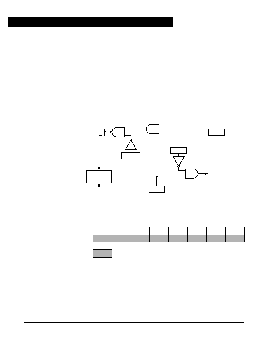
Low-Voltage Inhibit (LVI)
Data Sheet
MC68HC908GR16 -- Rev. 1.0
126
Low-Voltage Inhibit (LVI)
MOTOROLA
or V
DD
decreases to approximately 0 V which will re-trigger the power-on reset and
reset the trip point to 3-V operation.
LVISTOP, LVIPWRD, LVI5OR3, and LVIRSTD are in the configuration register
(CONFIG1). See
Figure 5-2. Configuration Register 1 (CONFIG1)
for details of
the LVI's configuration bits. Once an LVI reset occurs, the MCU remains in reset
until V
DD
rises above a voltage, V
TRIPR
, which causes the MCU to exit reset. See
15.3.2.5 Low-Voltage Inhibit (LVI) Reset
for details of the interaction between the
SIM and the LVI. The output of the comparator controls the state of the LVIOUT
flag in the LVI status register (LVISR).
An LVI reset also drives the RST pin low to provide low-voltage protection to
external peripheral devices.
Figure 11-1. LVI Module Block Diagram
LOW V
DD
DETECTOR
LVIPWRD
STOP INSTRUCTION
LVISTOP
LVI RESET
LVIOUT
V
DD
> LVI
Trip
= 0
V
DD
� LVI
Trip
= 1
FROM CONFIG
FROM CONFIG1
V
DD
FROM CONFIG1
LVIRSTD
LVI5OR3
FROM CONFIG1
Addr.
Register Name
Bit 7
6
5
4
3
2
1
Bit 0
$FE0C
LVI Status Register
(LVISR)
See page 127.
Read:
LVIOUT
0
0
0
0
0
0
0
Write:
Reset:
0
0
0
0
0
0
0
0
= Unimplemented
Figure 11-2. LVI I/O Register Summary

Low-Voltage Inhibit (LVI)
LVI Status Register
MC68HC908GR16 -- Rev. 1.0
Data Sheet
MOTOROLA
Low-Voltage Inhibit (LVI)
127
11.3.1 Polled LVI Operation
In applications that can operate at V
DD
levels below the V
TRIPF
level, software can
monitor V
DD
by polling the LVIOUT bit. In the configuration register, the LVIPWRD
bit must be at logic 0 to enable the LVI module, and the LVIRSTD bit must be at
logic 1 to disable LVI resets.
11.3.2 Forced Reset Operation
In applications that require V
DD
to remain above the V
TRIPF
level, enabling LVI
resets allows the LVI module to reset the MCU when V
DD
falls below the V
TRIPF
level. In the configuration register, the LVIPWRD and LVIRSTD bits must be at
logic 0 to enable the LVI module and to enable LVI resets.
11.3.3 Voltage Hysteresis Protection
Once the LVI has triggered (by having V
DD
fall below V
TRIPF
), the LVI will maintain
a reset condition until V
DD
rises above the rising trip point voltage, V
TRIPR
. This
prevents a condition in which the MCU is continually entering and exiting reset if
V
DD
is approximately equal to V
TRIPF
. V
TRIPR
is greater than V
TRIPF
by the
hysteresis voltage, V
HYS
.
11.3.4 LVI Trip Selection
The LVI5OR3 bit in the configuration register selects whether the LVI is configured
for 5-V or 3-V protection.
NOTE:
The microcontroller is guaranteed to operate at a minimum supply voltage. The trip
point (V
TRIPF
[5 V] or V
TRIPF
[3 V]) may be lower than this. See
Section 20.
Electrical Specifications
for the actual trip point voltages.
11.4 LVI Status Register
The LVI status register (LVISR) indicates if the V
DD
voltage was detected below
the V
TRIPF
level.
Address:
$FE0C
Bit 7
6
5
4
3
2
1
Bit 0
Read:
LVIOUT
0
0
0
0
0
0
0
Write:
Reset:
0
0
0
0
0
0
0
0
= Unimplemented
Figure 11-3. LVI Status Register (LVISR)

Low-Voltage Inhibit (LVI)
Data Sheet
MC68HC908GR16 -- Rev. 1.0
128
Low-Voltage Inhibit (LVI)
MOTOROLA
LVIOUT -- LVI Output Bit
This read-only flag becomes set when the V
DD
voltage falls below the V
TRIPF
trip voltage (see
Table 11-1
). Reset clears the LVIOUT bit.
11.5 LVI Interrupts
The LVI module does not generate interrupt requests.
11.6 Low-Power Modes
The STOP and WAIT instructions put the MCU in low power-consumption standby
modes.
11.6.1 Wait Mode
If enabled, the LVI module remains active in wait mode. If enabled to generate
resets, the LVI module can generate a reset and bring the MCU out of wait mode.
11.6.2 Stop Mode
If enabled in stop mode (LVISTOP set), the LVI module remains active in stop
mode. If enabled to generate resets, the LVI module can generate a reset and bring
the MCU out of stop mode.
Table 11-1. LVIOUT Bit Indication
V
DD
LVIOUT
V
DD
> V
TRIPR
0
V
DD
<
V
TRIPF
1
V
TRIPF
<
V
DD
<
V
TRIPR
Previous value

MC68HC908GR16 -- Rev. 1.0
Data Sheet
MOTOROLA
Input/Output Ports (PORTS)
129
Data Sheet -- MC68HC908GR16
Section 12. Input/Output Ports (PORTS)
12.1 Introduction
Bidirectional input-output (I/O) pins form five parallel ports. All I/O pins are
programmable as inputs or outputs. All individual bits within port A, port C, and
port D are software configurable with pullup devices if configured as input port bits.
The pullup devices are automatically and dynamically disabled when a port bit is
switched to output mode.
NOTE:
Connect any unused I/O pins to an appropriate logic level, either V
DD
or V
SS
.
Although the I/O ports do not require termination for proper operation, termination
reduces excess current consumption and the possibility of electrostatic damage.
Not all port pins are bonded out in all packages. Care sure be taken to make any
unbonded port pins an output to reduce them from being floating inputs.
Addr.
Register Name
Bit 7
6
5
4
3
2
1
Bit 0
$0000
Port A Data Register
(PTA)
See page 132.
Read:
PTA7
PTA6
PTA5
PTA4
PTA3
PTA2
PTA1
PTA0
Write:
Reset:
Unaffected by reset
$0001
Port B Data Register
(PTB)
See page 134.
Read:
PTB7
PTB6
PTB5
PTB4
PTB3
PTB2
PTB1
PTB0
Write:
Reset:
Unaffected by reset
$0002
Port C Data Register
(PTC)
See page 136.
Read:
0
PTC6
PTC5
PTC4
PTC3
PTC2
PTC1
PTC0
Write:
Reset:
Unaffected by reset
$0003
Port D Data Register
(PTD)
See page 138.
Read:
PTD7
PTD6
PTD5
PTD4
PTD3
PTD2
PTD1
PTD0
Write:
Reset:
Unaffected by reset
$0004
Data Direction Register A
(DDRA)
See page 132.
Read:
DDRA7
DDRA6
DDRA5
DDRA4
DDRA3
DDRA2
DDRA1
DDRA0
Write:
Reset:
0
0
0
0
0
0
0
0
= Unimplemented
Figure 12-1. I/O Port Register Summary
Input/Output Ports (PORTS)
Data Sheet
MC68HC908GR16 -- Rev. 1.0
130
Input/Output Ports (PORTS)
MOTOROLA
$0005
Data Direction Register B
(DDRB)
See page 135.
Read:
DDRB7
DDRB6
DDRB5
DDRB4
DDRB3
DDRB2
DDRB1
DDRB0
Write:
Reset:
0
0
0
0
0
0
0
0
$0006
Data Direction Register C
(DDRC)
See page 136.
Read:
0
DDRC6
DDRC5
DDRC4
DDRC3
DDRC2
DDRC1
DDRC0
Write:
Reset:
0
0
0
0
0
0
0
0
$0007
Data Direction Register D
(DDRD)
See page 139.
Read:
DDRD7
DDRD6
DDRD5
DDRD4
DDRD3
DDRD2
DDRD1
DDRD0
Write:
Reset:
0
0
0
0
0
0
0
0
$0008
Port E Data Register
(PTE)
See page 141.
Read:
0
0
PTE5
PTE4
PTE3
PTE2
PTE1
PTE0
Write:
Reset:
Unaffected by reset
$000C
Data Direction Register E
(DDRE)
See page 142.
Read:
0
0
DDRE5
DDRE4
DDRE3
DDRE2
DDRE1
DDRE0
Write:
Reset:
0
0
0
0
0
0
0
0
$000D
Port A Input Pullup Enable
Register (PTAPUE)
See page 134.
Read:
PTAPUE7
PTAPUE6
PTAPUE5
PTAPUE4
PTAPUE3
PTAPUE2
PTAPUE1
PTAPUE0
Write:
Reset:
0
0
0
0
0
0
0
0
$000E
Port C Input Pullup Enable
Register (PTCPUE)
See page 138.
Read:
0
PTCPUE6
PTCPUE5
PTCPUE4
PTCPUE3
PTCPUE2
PTCPUE1
PTCPUE0
Write:
Reset:
0
0
0
0
0
0
0
0
$000F
Port D Input Pullup Enable
Register (PTDPUE)
See page 141.
Read:
PTDPUE7
PTDPUE6
PTDPUE5
PTDPUE4
PTDPUE3
PTDPUE2
PTDPUE1
PTDPUE0
Write:
Reset:
0
0
0
0
0
0
0
0
Addr.
Register Name
Bit 7
6
5
4
3
2
1
Bit 0
= Unimplemented
Figure 12-1. I/O Port Register Summary (Continued)
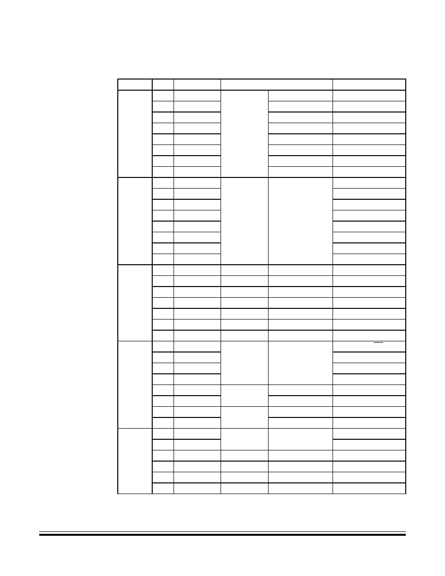
Input/Output Ports (PORTS)
Introduction
MC68HC908GR16 -- Rev. 1.0
Data Sheet
MOTOROLA
Input/Output Ports (PORTS)
131
Table 12-1. Port Control Register Bits Summary
Port
Bit
DDR
Module Control
Pin
A
0
DDRA0
KBD
KBIE0
PTA0/KBD0
1
DDRA1
KBIE1
PTA1/KBD1
2
DDRA2
KBIE2
PTA2/KBD2
3
DDRA3
KBIE3
PTA3/KBD3
4
DDRA4
KBIE4
PTA4/KBD4
5
DDRA5
KBIE5
PTA5/KBD5
6
DDRA6
KBIE6
PTA6/KBD6
7
DDRA7
KBIE7
PTA7/KBD7
B
0
DDRB0
ADC
ADCH4�ADCH0
PTB0/AD0
1
DDRB1
PTB1/AD1
2
DDRB2
PTB2/AD2
3
DDRB3
PTB3/AD3
4
DDRB4
PTB4/AD4
5
DDRB5
PTB5/AD5
6
DDRB6
PTB6/AD6
7
DDRB7
PTB7/AD7
C
0
DDRC0
PTC0
1
DDRC1
PTC1
2
DDRC2
PTC2
3
DDRC3
PTC3
4
DDRC4
PTC4
5
DDRC5
PTC5
6
DDRC6
PTC6
D
0
DDRD0
SPI
SPE
PTD0/SS
1
DDRD1
PTD1/MISO
2
DDRD2
PTD2/MOSI
3
DDRD3
PTD3/SPSCK
4
DDRD4
TIM1
ELS0B:ELS0A
PTD4/T1CH0
5
DDRD5
ELS1B:ELS1A
PTD5/T1CH1
6
DDRD6
TIM2
ELS0B:ELS0A
PTD6/T2CH0
7
DDRD7
ELS1B:ELS1A
PTD7/T2CH1
E
0
DDRE0
SCI
ENSCI
PTE0/TxD
1
DDRE1
PTE1/RxD
2
DDRE2
PTE2
3
DDRE3
PTE3
4
DDRE4
PTE4
5
DDRE5
PTE5

Input/Output Ports (PORTS)
Data Sheet
MC68HC908GR16 -- Rev. 1.0
132
Input/Output Ports (PORTS)
MOTOROLA
12.2 Port A
Port A is an 8-bit special-function port that shares all eight of its pins with the
keyboard interrupt (KBI) module. Port A also has software configurable pullup
devices if configured as an input port.
12.2.1 Port A Data Register
The port A data register (PTA) contains a data latch for each of the eight port A
pins.
PTA7�PTA0 -- Port A Data Bits
These read/write bits are software programmable. Data direction of each port A
pin is under the control of the corresponding bit in data direction register A.
Reset has no effect on port A data.
KBD7�KBD0 -- Keyboard Inputs
The keyboard interrupt enable bits, KBIE7�KBIE0, in the keyboard interrupt
control register (KBICR) enable the port A pins as external interrupt pins. See
Section 9. Keyboard Interrupt Module (KBI).
12.2.2 Data Direction Register A
Data direction register A (DDRA) determines whether each port A pin is an input or
an output. Writing a logic 1 to a DDRA bit enables the output buffer for the
corresponding port A pin; a logic 0 disables the output buffer.
DDRA7�DDRA0 -- Data Direction Register A Bits
These read/write bits control port A data direction. Reset clears
DDRA7�DDRA0, configuring all port A pins as inputs.
1 = Corresponding port A pin configured as output
0 = Corresponding port A pin configured as input
Address:
$0000
Bit 7
6
5
4
3
2
1
Bit 0
Read:
PTA7
PTA6
PTA5
PTA4
PTA3
PTA2
PTA1
PTA0
Write:
Reset:
Unaffected by reset
Alternate
Function:
KBD7
KBD6
KBD5
KBD4
KBD3
KBD2
KBD1
KBD0
Figure 12-2. Port A Data Register (PTA)
Address:
$0004
Bit 7
6
5
4
3
2
1
Bit 0
Read:
DDRA7
DDRA6
DDRA5
DDRA4
DDRA3
DDRA2
DDRA1
DDRA0
Write:
Reset:
0
0
0
0
0
0
0
0
Figure 12-3. Data Direction Register A (DDRA)
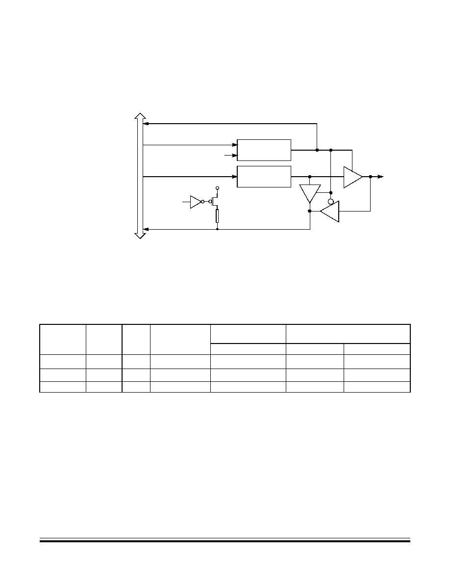
Input/Output Ports (PORTS)
Port A
MC68HC908GR16 -- Rev. 1.0
Data Sheet
MOTOROLA
Input/Output Ports (PORTS)
133
NOTE:
Avoid glitches on port A pins by writing to the port A data register before changing
data direction register A bits from 0 to 1.
Figure 12-4
shows the port A I/O logic.
Figure 12-4. Port A I/O Circuit
When bit DDRAx is a logic 1, reading address $0000 reads the PTAx data latch.
When bit DDRAx is a logic 0, reading address $0000 reads the voltage level on the
pin. The data latch can always be written, regardless of the state of its data
direction bit.
Table 12-2
summarizes the operation of the port A pins.
12.2.3 Port A Input Pullup Enable Register
The port A input pullup enable register (PTAPUE) contains a software configurable
pullup device for each of the eight port A pins. Each bit is individually configurable
and requires that the data direction register, DDRA, bit be configured as an input.
Each pullup is automatically and dynamically disabled when a port bit's DDRA is
configured for output mode.
READ DDRA ($0004)
WRITE DDRA ($0004)
RESET
WRITE PTA ($0000)
READ PTA ($0000)
PTAx
DDRAx
PTAx
INT
ERNAL DATA BUS
V
DD
PTAPUEx
INTERNAL
PULLUP
DEVICE
Table 12-2. Port A Pin Functions
PTAPUE
Bit
DDRA
Bit
PTA
Bit
I/O Pin
Mode
Accesses
to DDRA
Accesses
to PTA
Read/Write
Read
Write
1
0
X
(1)
Input, V
DD
(2)
DDRA7�DDRA0
Pin
PTA7�PTA0
(3)
0
0
X
Input, Hi-Z
(4)
DDRA7�DDRA0
Pin
PTA7�PTA0
(3)
X
1
X
Output
DDRA7�DDRA0
PTA7�PTA0
PTA7�PTA0
1. X = Don't care
2. I/O pin pulled up to V
DD
by internal pullup device
3. Writing affects data register, but does not affect input.
4. Hi-Z = High impedance
Input/Output Ports (PORTS)
Data Sheet
MC68HC908GR16 -- Rev. 1.0
134
Input/Output Ports (PORTS)
MOTOROLA
PTAPUE7�PTAPUE0 -- Port A Input Pullup Enable Bits
These writable bits are software programmable to enable pullup devices on an
input port bit.
1 = Corresponding port A pin configured to have internal pullup
0 = Corresponding port A pin has internal pullup disconnected
12.3 Port B
Port B is an 8-bit special-function port that shares six of its pins with the
analog-to-digital converter (ADC) module.
12.3.1 Port B Data Register
The port B data register (PTB) contains a data latch for each of the eight port pins.
PTB7�PTB0 -- Port B Data Bits
These read/write bits are software-programmable. Data direction of each port B
pin is under the control of the corresponding bit in data direction register B.
Reset has no effect on port B data.
AD7�AD0 -- Analog-to-Digital Input Bits
AD7�AD0 are pins used for the input channels to the analog-to-digital converter
module. The channel select bits in the ADC status and control register define
which port B pin will be used as an ADC input and overrides any control from
the port I/O logic by forcing that pin as the input to the analog circuitry.
NOTE:
Care must be taken when reading port B while applying analog voltages to
AD7�AD0 pins. If the appropriate ADC channel is not enabled, excessive current
drain may occur if analog voltages are applied to the PTBx/ADx pin, while PTB is
read as a digital input. Those ports not selected as analog input channels are
considered digital I/O ports.
Address:
$000D
Bit 7
6
5
4
3
2
1
Bit 0
Read:
PTAPUE7
PTAPUE6
PTAPUE5
PTAPUE4
PTAPUE3
PTAPUE2
PTAPUE1
PTAPUE0
Write:
Reset:
0
0
0
0
0
0
0
0
Figure 12-5. Port A Input Pullup Enable Register (PTAPUE)
Address:
$0001
Bit 7
6
5
4
3
2
1
Bit 0
Read:
PTB7
PTB6
PTB5
PTB4
PTB3
PTB2
PTB1
PTB0
Write:
Reset:
Unaffected by reset
Alternate
Function:
AD7
AD6
AD5
AD4
AD3
AD2
AD1
AD0
Figure 12-6. Port B Data Register (PTB)
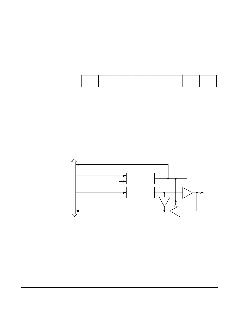
Input/Output Ports (PORTS)
Port B
MC68HC908GR16 -- Rev. 1.0
Data Sheet
MOTOROLA
Input/Output Ports (PORTS)
135
12.3.2 Data Direction Register B
Data direction register B (DDRB) determines whether each port B pin is an input or
an output. Writing a logic 1 to a DDRB bit enables the output buffer for the
corresponding port B pin; a logic 0 disables the output buffer.
DDRB7�DDRB0 -- Data Direction Register B Bits
These read/write bits control port B data direction. Reset clears
DDRB7�DDRB0, configuring all port B pins as inputs.
1 = Corresponding port B pin configured as output
0 = Corresponding port B pin configured as input
NOTE:
Avoid glitches on port B pins by writing to the port B data register before changing
data direction register B bits from 0 to 1.
Figure 12-8
shows the port B I/O logic.
Figure 12-8. Port B I/O Circuit
When bit DDRBx is a logic 1, reading address $0001 reads the PTBx data latch.
When bit DDRBx is a logic 0, reading address $0001 reads the voltage level on the
pin. The data latch can always be written, regardless of the state of its data
direction bit.
Table 12-3
summarizes the operation of the port B pins.
Address:
$0005
Bit 7
6
5
4
3
2
1
Bit 0
Read:
DDRB7
DDRB6
DDRB5
DDRB4
DDRB3
DDRB2
DDRB1
DDRB0
Write:
Reset:
0
0
0
0
0
0
0
0
Figure 12-7. Data Direction Register B (DDRB)
READ DDRB ($0005)
WRITE DDRB ($0005)
RESET
WRITE PTB ($0001)
READ PTB ($0001)
PTBx
DDRBx
PTBx
INTERNA
L DA
TA
BUS
Input/Output Ports (PORTS)
Data Sheet
MC68HC908GR16 -- Rev. 1.0
136
Input/Output Ports (PORTS)
MOTOROLA
12.4 Port C
Port C is a 7-bit, general-purpose bidirectional I/O port. Port C also has software
configurable pullup devices if configured as an input port.
12.4.1 Port C Data Register
The port C data register (PTC) contains a data latch for each of the port C pins.
PTC6 and PTC0 -- Port C Data Bits
These read/write bits are software-programmable. Data direction of each port C
pin is under the control of the corresponding bit in data direction register C.
Reset has no effect on port C data.
12.4.2 Data Direction Register C
Data direction register C (DDRC) determines whether each port C pin is an input
or an output. Writing a logic 1 to a DDRC bit enables the output buffer for the
corresponding port C pin; a logic 0 disables the output buffer.
Table 12-3. Port B Pin Functions
DDRB
Bit
PTB
Bit
I/O Pin
Mode
Accesses
to DDRB
Accesses
to PTB
Read/Write
Read
Write
0
X
(1)
1. X = Don't care
Input, Hi-Z
(2)
2. Hi-Z = High impedance
DDRB7�DDRB0
Pin
PTB7�PTB0
(3)
3. Writing affects data register, but does not affect input.
1
X
Output
DDRB7�DDRB0
PTB7�PTB0
PTB7�PTB0
Address:
$0002
Bit 7
6
5
4
3
2
1
Bit 0
Read:
0
PTC6
PTC5
PTC4
PTC3
PTC2
PTC1
PTC0
Write:
Reset:
Unaffected by reset
= Unimplemented
R
= Reserved
Figure 12-9. Port C Data Register (PTC)
Address:
$0006
Bit 7
6
5
4
3
2
1
Bit 0
Read:
0
DDRC6
DDRC5
DDRC4
DDRC3
DDRC2
DDRC1
DDRC0
Write:
Reset:
0
0
0
0
0
0
0
0
= Unimplemented
Figure 12-10. Data Direction Register C (DDRC)
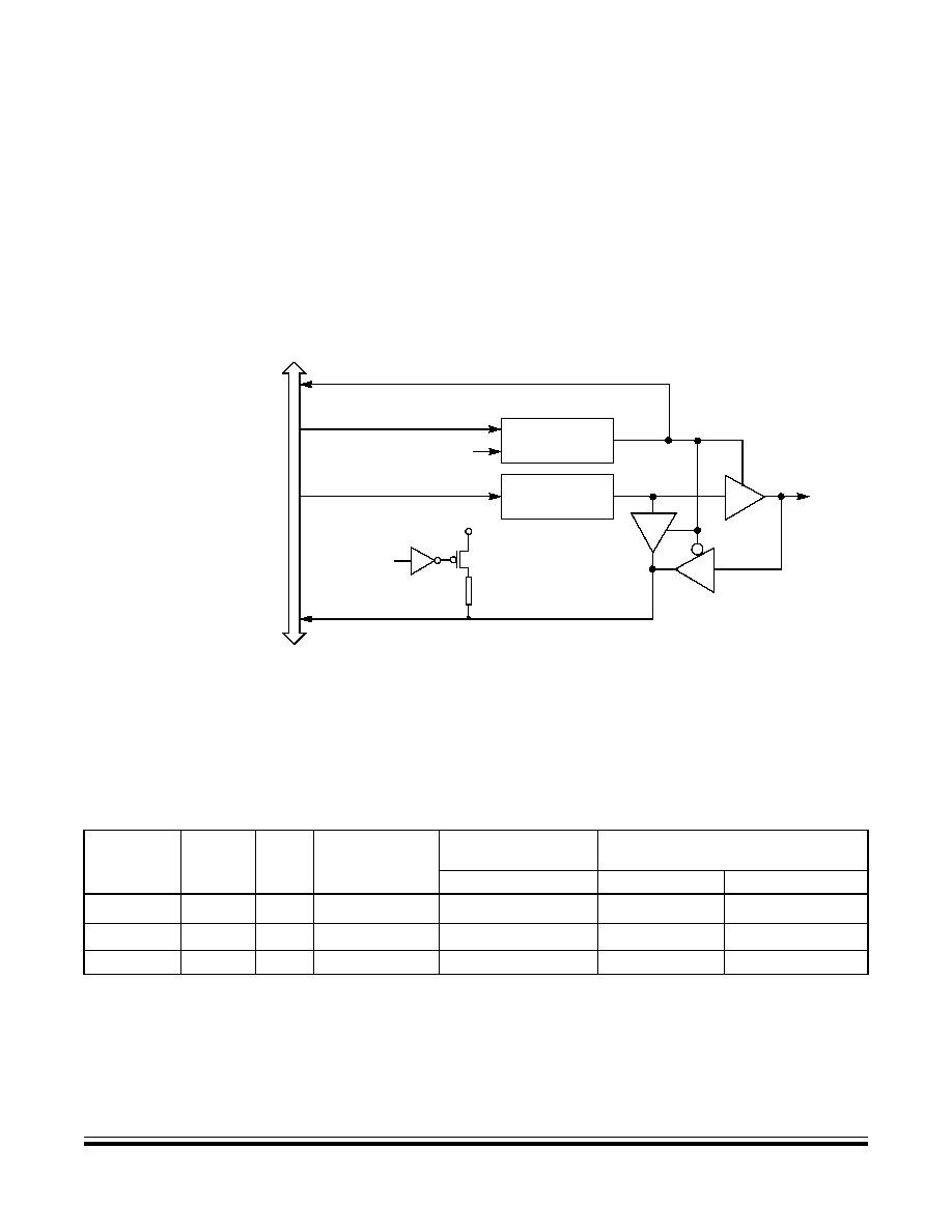
Input/Output Ports (PORTS)
Port C
MC68HC908GR16 -- Rev. 1.0
Data Sheet
MOTOROLA
Input/Output Ports (PORTS)
137
DDRC6 and DDRC0 -- Data Direction Register C Bits
These read/write bits control port C data direction. Reset clears DDRC6 and
DDRC0, configuring all port C pins as inputs.
1 = Corresponding port C pin configured as output
0 = Corresponding port C pin configured as input
NOTE:
Avoid glitches on port C pins by writing to the port C data register before changing
data direction register C bits from 0 to 1.
Figure 12-11
shows the port C I/O logic.
Figure 12-11. Port C I/O Circuit
When bit DDRCx is a logic 1, reading address $0002 reads the PTCx data latch.
When bit DDRCx is a logic 0, reading address $0002 reads the voltage level on the
pin. The data latch can always be written, regardless of the state of its data
direction bit.
Table 12-4
summarizes the operation of the port C pins.
READ DDRC ($0006)
WRITE DDRC ($0006)
RESET
WRITE PTC ($0002)
READ PTC ($0002)
PTCx
DDRCx
PTCx
INTE
RNAL D
A
T
A
B
U
S
V
DD
INTERNAL
PTCPUEx
PULLUP
DEVICE
Table 12-4. Port C Pin Functions
PTCPUE
Bit
DDRC
Bit
PTC
Bit
I/O Pin
Mode
Accesses
to DDRC
Accesses
to PTC
Read/Write
Read
Write
1
0
X
(1)
Input, V
DD
(2)
DDRC6�DDRC0
Pin
PTC6�PTC0
(3)
0
0
X
Input, Hi-Z
(4)
DDRC6�DDRC0
Pin
PTC6�PTC0
(3)
X
1
X
Output
DDRC6�DDRC0
PTC6�PTC0
PTC6�PTC0
1. X = Don't care
2. I/O pin pulled up to V
DD
by internal pullup device.
3. Writing affects data register, but does not affect input.
4. Hi-Z = High impedance
Input/Output Ports (PORTS)
Data Sheet
MC68HC908GR16 -- Rev. 1.0
138
Input/Output Ports (PORTS)
MOTOROLA
12.4.3 Port C Input Pullup Enable Register
The port C input pullup enable register (PTCPUE) contains a software configurable
pullup device for each of the port C pins. Each bit is individually configurable and
requires that the data direction register, DDRC, bit be configured as an input. Each
pullup is automatically and dynamically disabled when a port bit's DDRC is
configured for output mode.
PTCPUE1 and PTCPUE0 -- Port C Input Pullup Enable Bits
These writable bits are software programmable to enable pullup devices on an
input port bit.
1 = Corresponding port C pin configured to have internal pullup
0 = Corresponding port C pin internal pullup disconnected
12.5 Port D
Port D is an 8-bit special-function port that shares four of its pins with the serial
peripheral interface (SPI) module and three of its pins with two timer interface
(TIM1 and TIM2) modules. Port D also has software configurable pullup devices if
configured as an input port.
12.5.1 Port D Data Register
The port D data register (PTD) contains a data latch for each of the eight port D
pins.
PTD7�PTD0 -- Port D Data Bits
These read/write bits are software-programmable. Data direction of each port D
pin is under the control of the corresponding bit in data direction register D.
Reset has no effect on port D data.
Address:
$000E
Bit 7
6
5
4
3
2
1
Bit 0
Read:
0
PTCPUE6
PTCPUE5
PTCPUE4
PTCPUE3
PTCPUE2
PTCPUE1
PTCPUE0
Write:
Reset:
0
0
0
0
0
0
0
0
= Unimplemented
Figure 12-12. Port C Input Pullup Enable Register (PTCPUE)
Address:
$0003
Bit 7
6
5
4
3
2
1
Bit 0
Read:
PTD7
PTD6
PTD5
PTD4
PTD3
PTD2
PTD1
PTD0
Write:
Reset:
Unaffected by reset
Alternate
Function:
T2CH1
T2CH0
T1CH1
T1CH0
SPSCK
MOSI
MISO
SS
Figure 12-13. Port D Data Register (PTD)

Input/Output Ports (PORTS)
Port D
MC68HC908GR16 -- Rev. 1.0
Data Sheet
MOTOROLA
Input/Output Ports (PORTS)
139
T2CH1 and T2CH0 -- Timer 2 Channel I/O Bits
The PTD6/T2CH0�PTD7/T2CH1 pins are the TIM2 input capture/output
compare pins. The edge/level select bits, ELSxB and ELSxA, determine
whether the PTD6/T2CH0�PTD7/T2CH1 pins are timer channel I/O pins or
general-purpose I/O pin. See
Section 18. Timer Interface Module (TIM)
.
T1CH1 and T1CH0 -- Timer 1 Channel I/O Bits
The PTD4/T1CH0�PTD5/T1CH1 pins are the TIM1 input capture/output
compare pins. The edge/level select bits, ELSxB and ELSxA, determine
whether the PTD4/T1CH0�PTD5/T1CH1 pins are timer channel I/O pins or
general-purpose I/O pins. See
Section 18. Timer Interface Module (TIM)
.
SPSCK -- SPI Serial Clock
The PTD3/SPSCK pin is the serial clock input of the SPI module. When the SPE
bit is clear, the PTD3/SPSCK pin is available for general-purpose I/O.
MOSI -- Master Out/Slave In
The PTD2/MOSI pin is the master out/slave in terminal of the SPI module. When
the SPE bit is clear, the PTD2/MOSI pin is available for general-purpose I/O.
MISO -- Master In/Slave Out
The PTD1/MISO pin is the master in/slave out terminal of the SPI module. When
the SPI enable bit, SPE, is clear, the SPI module is disabled, and the PTD0/SS
pin is available for general-purpose I/O.
Data direction register D (DDRD) does not affect the data direction of port D pins
that are being used by the SPI module. However, the DDRD bits always
determine whether reading port D returns the states of the latches or the states
of the pins. See
Table 12-5
.
SS -- Slave Select
The PTD0/SS pin is the slave select input of the SPI module. When the SPE bit
is clear, or when the SPI master bit, SPMSTR, is set, the PTD0/SS pin is
available for general-purpose I/O. When the SPI is enabled, the DDRB0 bit in
data direction register B (DDRB) has no effect on the PTD0/SS pin.
12.5.2 Data Direction Register D
Data direction register D (DDRD) determines whether each port D pin is an input
or an output. Writing a logic 1 to a DDRD bit enables the output buffer for the
corresponding port D pin; a logic 0 disables the output buffer.
Address:
$0007
Bit 7
6
5
4
3
2
1
Bit 0
Read:
DDRD7
DDRD6
DDRD5
DDRD4
DDRD3
DDRD2
DDRD1
DDRD0
Write:
Reset:
0
0
0
0
0
0
0
0
Figure 12-14. Data Direction Register D (DDRD)
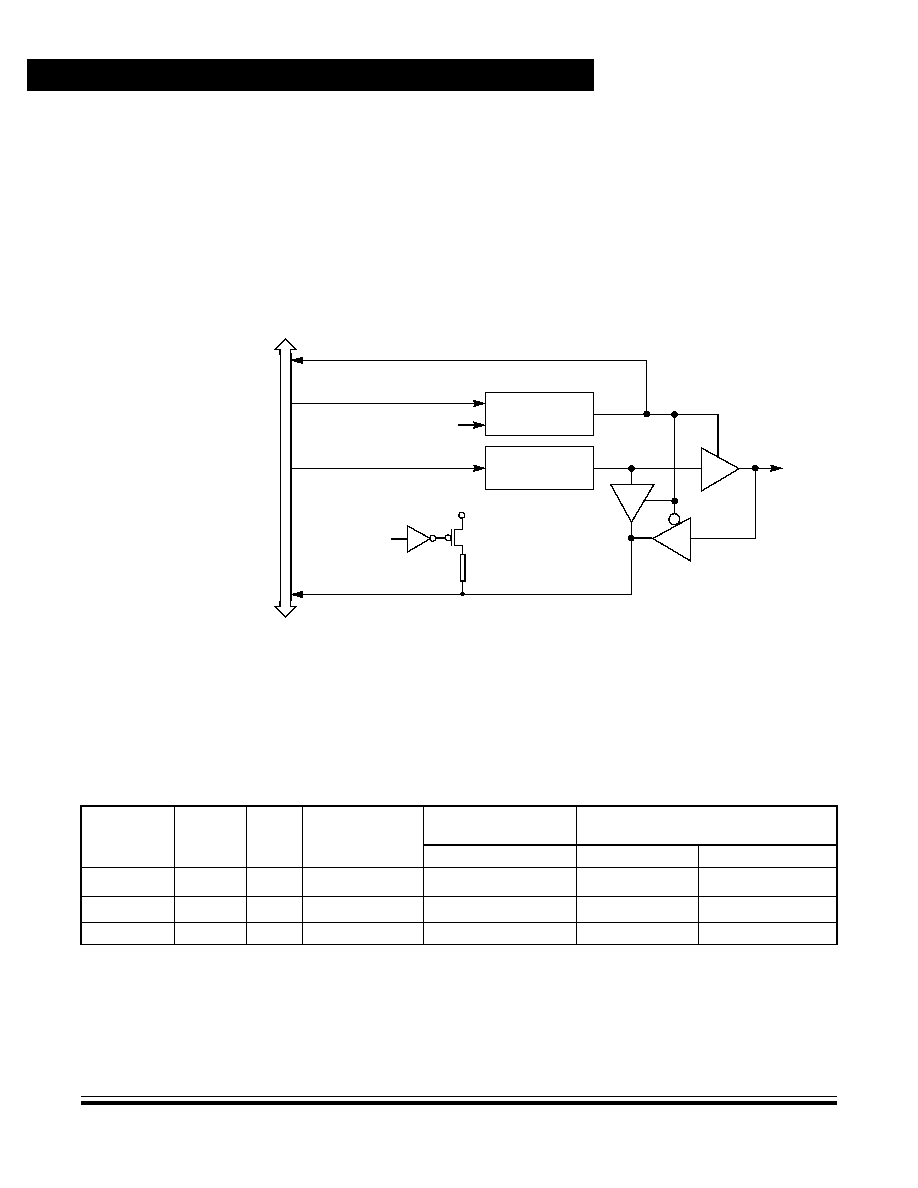
Input/Output Ports (PORTS)
Data Sheet
MC68HC908GR16 -- Rev. 1.0
140
Input/Output Ports (PORTS)
MOTOROLA
DDRD7�DDRD0 -- Data Direction Register D Bits
These read/write bits control port D data direction. Reset clears
DDRD7�DDRD0, configuring all port D pins as inputs.
1 = Corresponding port D pin configured as output
0 = Corresponding port D pin configured as input
NOTE:
Avoid glitches on port D pins by writing to the port D data register before changing
data direction register D bits from 0 to 1.
Figure 12-15
shows the port D I/O logic.
Figure 12-15. Port D I/O Circuit
When bit DDRDx is a logic 1, reading address $0003 reads the PTDx data latch.
When bit DDRDx is a logic 0, reading address $0003 reads the voltage level on the
pin. The data latch can always be written, regardless of the state of its data
direction bit.
Table 12-5
summarizes the operation of the port D pins.
READ DDRD ($0007)
WRITE DDRD ($0007)
RESET
WRITE PTD ($0003)
READ PTD ($0003)
PTDx
DDRDx
PTDx
INTERN
AL DATA BUS
VDD
INTERNAL
PTDPUEx
PULLUP
DEVICE
Table 12-5. Port D Pin Functions
PTDPUE
Bit
DDRD
Bit
PTD
Bit
I/O Pin
Mode
Accesses
to DDRD
Accesses
to PTD
Read/Write
Read
Write
1
0
X
(1)
Input, V
DD
(2)
DDRD7�DDRD0
Pin
PTD7�PTD0
(3)
0
0
X
Input, Hi-Z
(4)
DDRD7�DDRD0
Pin
PTD7�PTD0
(3)
X
1
X
Output
DDRD7�DDRD0
PTD7�PTD0
PTD7�PTD0
1. X = Don't care
2. I/O pin pulled up to V
DD
by internal pullup device.
3. Writing affects data register, but does not affect input.
4. Hi-Z = High imp[edance
Input/Output Ports (PORTS)
Port E
MC68HC908GR16 -- Rev. 1.0
Data Sheet
MOTOROLA
Input/Output Ports (PORTS)
141
12.5.3 Port D Input Pullup Enable Register
The port D input pullup enable register (PTDPUE) contains a software configurable
pullup device for each of the eight port D pins. Each bit is individually configurable
and requires that the data direction register, DDRD, bit be configured as an input.
Each pullup is automatically and dynamically disabled when a port bit's DDRD is
configured for output mode.
PTDPUE7�PTDPUE0 -- Port D Input Pullup Enable Bits
These writable bits are software programmable to enable pullup devices on an
input port bit.
1 = Corresponding port D pin configured to have internal pullup
0 = Corresponding port D pin has internal pullup disconnected
12.6 Port E
Port E is a 6-bit special-function port that shares two of its pins with the enhanced
serial communications interface (ESCI) module.
12.6.1 Port E Data Register
The port E data register contains a data latch for each of the six port E pins.
PTE5�PTE0 -- Port E Data Bits
These read/write bits are software-programmable. Data direction of each port E
pin is under the control of the corresponding bit in data direction register E.
Reset has no effect on port E data.
Address:
$000F
Bit 7
6
5
4
3
2
1
Bit 0
Read:
PTDPUE7
PTDPUE6
PTDPUE5
PTDPUE4
PTDPUE3
PTDPUE2
PTDPUE1
PTDPUE0
Write:
Reset:
0
0
0
0
0
0
0
0
Figure 12-16. Port D Input Pullup Enable Register (PTDPUE)
Address:
$0008
Bit 7
6
5
4
3
2
1
Bit 0
Read:
0
0
PTE5
PTE4
PTE3
PTE2
PTE1
PTE0
Write:
Reset:
Unaffected by reset
Alternate
Function:
RxD
TxD
= Unimplemented
Figure 12-17. Port E Data Register (PTE)
Input/Output Ports (PORTS)
Data Sheet
MC68HC908GR16 -- Rev. 1.0
142
Input/Output Ports (PORTS)
MOTOROLA
NOTE:
Data direction register E (DDRE) does not affect the data direction of port E pins
that are being used by the ESCI module. However, the DDRE bits always
determine whether reading port E returns the states of the latches or the states of
the pins. See
Table 12-6
.
RxD -- SCI Receive Data Input
The PTE1/RxD pin is the receive data input for the ESCI module. When the
enable SCI bit, ENSCI, is clear, the ESCI module is disabled, and the PTE1/RxD
pin is available for general-purpose I/O. See
Section 14. Enhanced Serial
Communications Interface (ESCI) Module
.
TxD -- SCI Transmit Data Output
The PTE0/TxD pin is the transmit data output for the ESCI module. When the
enable SCI bit, ENSCI, is clear, the ESCI module is disabled, and the PTE0/TxD
pin is available for general-purpose I/O. See
Section 14. Enhanced Serial
Communications Interface (ESCI) Module
.
12.6.2 Data Direction Register E
Data direction register E (DDRE) determines whether each port E pin is an input or
an output. Writing a logic 1 to a DDRE bit enables the output buffer for the
corresponding port E pin; a logic 0 disables the output buffer.
DDRE5�DDRE0 -- Data Direction Register E Bits
These read/write bits control port E data direction. Reset clears
DDRE5�DDRE0, configuring all port E pins as inputs.
1 = Corresponding port E pin configured as output
0 = Corresponding port E pin configured as input
NOTE:
Avoid glitches on port E pins by writing to the port E data register before changing
data direction register E bits from 0 to 1.
Figure 12-19
shows the port E I/O logic.
Address:
$000C
Bit 7
6
5
4
3
2
1
Bit 0
Read:
0
0
DDRE5
DDRE4
DDRE3
DDRE2
DDRE1
DDRE0
Write:
Reset:
0
0
0
0
0
0
0
0
= Unimplemented
Figure 12-18. Data Direction Register E (DDRE)
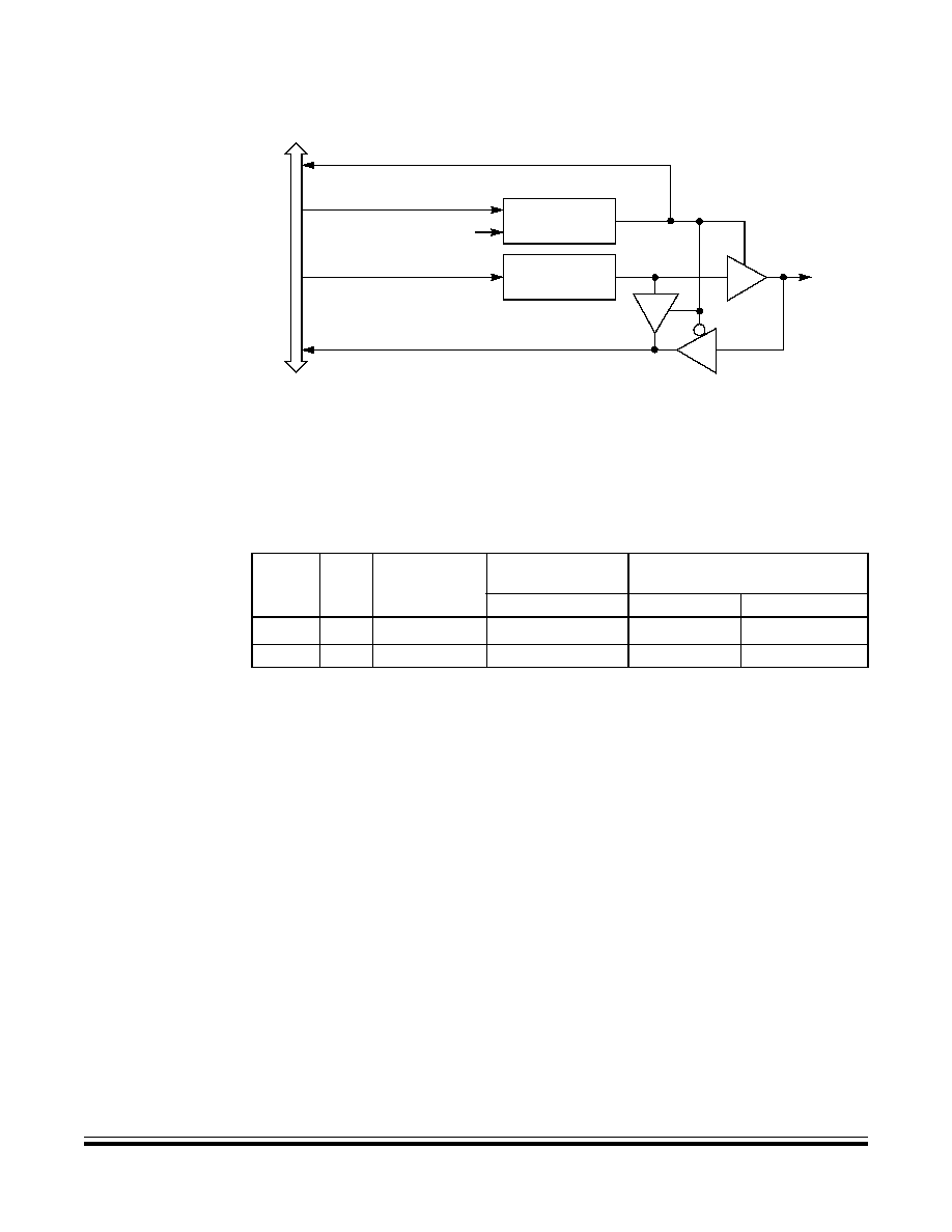
Input/Output Ports (PORTS)
Port E
MC68HC908GR16 -- Rev. 1.0
Data Sheet
MOTOROLA
Input/Output Ports (PORTS)
143
Figure 12-19. Port E I/O Circuit
When bit DDREx is a logic 1, reading address $0008 reads the PTEx data latch.
When bit DDREx is a logic 0, reading address $0008 reads the voltage level on the
pin. The data latch can always be written, regardless of the state of its data
direction bit.
Table 12-6
summarizes the operation of the port E pins.
Table 12-6. Port E Pin Functions
DDRE
Bit
PTE
Bit
I/O Pin
Mode
Accesses
to DDRE
Accesses
to PTE
Read/Write
Read
Write
0
X
(1)
1. X = Don't care
Input, Hi-Z
(2)
2. Hi-Z = High impedance
DDRE5�DDRE0
Pin
PTE5�PTE0
(3)
3. Writing affects data register, but does not affect input.
1
X
Output
DDRE5�DDRE0
PTE5�PTE0
PTE5�PTE0
READ DDRE ($000C)
WRITE DDRE ($000C)
RESET
WRITE PTE ($0008)
READ PTE ($0008)
PTEx
DDREx
PTEx
INT
ERNAL DATA BUS

Input/Output Ports (PORTS)
Data Sheet
MC68HC908GR16 -- Rev. 1.0
144
Input/Output Ports (PORTS)
MOTOROLA

MC68HC908GR16 -- Rev. 1.0
Data Sheet
MOTOROLA
Resets and Interrupts
145
Data Sheet -- MC68HC908GR16
Section 13. Resets and Interrupts
13.1 Introduction
Resets and interrupts are responses to exceptional events during program
execution. A reset re-initializes the microcontroller (MCU) to its startup condition.
An interrupt vectors the program counter to a service routine.
13.2 Resets
A reset immediately returns the MCU to a known startup condition and begins
program execution from a user-defined memory location.
13.2.1 Effects
A reset:
�
Immediately stops the operation of the instruction being executed
�
Initializes certain control and status bits
�
Loads the program counter with a user-defined reset vector address from
locations $FFFE and $FFFF
�
Selects CGMXCLK divided by four as the bus clock
13.2.2 External Reset
A logic 0 applied to the RST pin for a time, t
RL
, generates an external reset. An
external reset sets the PIN bit in the system integration module (SIM) reset status
register.
13.2.3 Internal Reset
Sources:
�
Power-on reset (POR)
�
Computer operating properly (COP)
�
Low-power reset circuits
�
Illegal opcode
�
Illegal address
All internal reset sources pull the RST pin low for 32 CGMXCLK cycles to allow
resetting of external devices. The MCU is held in reset for an additional 32
CGMXCLK cycles after releasing the RST pin.
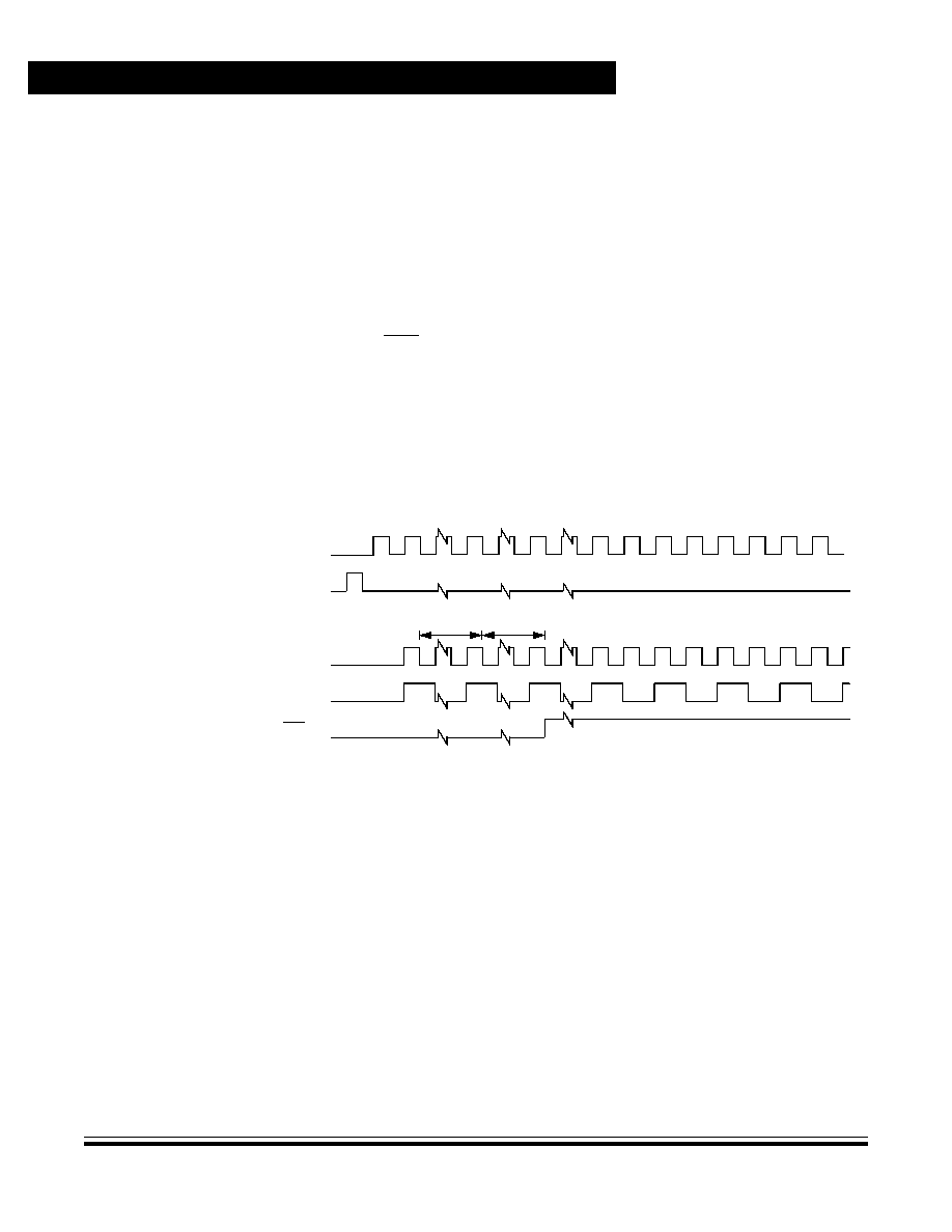
Resets and Interrupts
Data Sheet
MC68HC908GR16 -- Rev. 1.0
146
Resets and Interrupts
MOTOROLA
13.2.3.1 Power-On Reset (POR)
A power-on reset (POR) is an internal reset caused by a positive transition on the
V
DD
pin. V
DD
at the POR must go below V
POR
to reset the MCU. This distinguishes
between a reset and a POR. The POR is not a brown-out detector, low-voltage
detector, or glitch detector.
A power-on reset:
�
Holds the clocks to the central processor unit (CPU) and modules inactive
for an oscillator stabilization delay of 4096 CGMXCLK cycles
�
Drives the RST pin low during the oscillator stabilization delay
�
Releases the RST pin 32 CGMXCLK cycles after the oscillator stabilization
delay
�
Releases the CPU to begin the reset vector sequence 64 CGMXCLK cycles
after the oscillator stabilization delay
�
Sets the POR and LVI bits in the SIM reset status register and clears all
other bits in the register
Figure 13-1. Power-On Reset Recovery
13.2.3.2 Computer Operating Properly (COP) Reset
A computer operating properly (COP) reset is an internal reset caused by an
overflow of the COP counter. A COP reset sets the COP bit in the SIM reset status
register.
To clear the COP counter and prevent a COP reset, write any value to the COP
control register at location $FFFF.
PORRST
(1)
OSC1
CGMXCLK
CGMOUT
RST PIN
4096
CYCLES
32
CYCLES
1. PORRST is an internally generated power-on reset pulse.

Resets and Interrupts
Resets
MC68HC908GR16 -- Rev. 1.0
Data Sheet
MOTOROLA
Resets and Interrupts
147
13.2.3.3 Low-Voltage Inhibit (LVI) Reset
A low-voltage inhibit (LVI) reset is an internal reset caused by a drop in the power
supply voltage to the LVI
TRIPF
voltage.
An LVI reset:
�
Holds the clocks to the CPU and modules inactive for an oscillator
stabilization delay of 4096 CGMXCLK cycles after the power supply voltage
rises to the LVI
TRIPR
voltage
�
Drives the RST pin low for as long as V
DD
is below the LVI
TRIPR
voltage and
during the oscillator stabilization delay
�
Releases the RST pin 32 CGMXCLK cycles after the oscillator stabilization
delay
�
Releases the CPU to begin the reset vector sequence 64 CGMXCLK cycles
after the oscillator stabilization delay
�
Sets the LVI bit in the SIM reset status register
13.2.3.4 Illegal Opcode Reset
An illegal opcode reset is an internal reset caused by an opcode that is not in the
instruction set. An illegal opcode reset sets the ILOP bit in the SIM reset status
register.
If the stop enable bit, STOP, in the mask option register is a logic 0, the STOP
instruction causes an illegal opcode reset.
13.2.3.5 Illegal Address Reset
An illegal address reset is an internal reset caused by opcode fetch from an
unmapped address. An illegal address reset sets the ILAD bit in the SIM reset
status register.
A data fetch from an unmapped address does not generate a reset.
13.2.4 System Integration Module (SIM) Reset Status Register
This read-only register contains flags to show reset sources. All flag bits are
automatically cleared following a read of the register. Reset service can read the
SIM reset status register to clear the register after power-on reset and to determine
the source of any subsequent reset.
The register is initialized on power-up as shown with the POR bit set and all other
bits cleared. During a POR or any other internal reset, the RST pin is pulled low.
After the pin is released, it will be sampled 32 CGMXCLK cycles later. If the pin is
not above a V
IH
at that time, then the PIN bit in the SRSR may be set in addition to
whatever other bits are set.
NOTE:
Only a read of the SIM reset status register clears all reset flags. After multiple
resets from different sources without reading the register, multiple flags remain set.

Resets and Interrupts
Data Sheet
MC68HC908GR16 -- Rev. 1.0
148
Resets and Interrupts
MOTOROLA
POR -- Power-On Reset Flag
1 = Power-on reset since last read of SRSR
0 = Read of SRSR since last power-on reset
PIN -- External Reset Flag
1 = External reset via RST pin since last read of SRSR
0 = POR or read of SRSR since last external reset
COP -- Computer Operating Properly Reset Bit
1 = Last reset caused by timeout of COP counter
0 = POR or read of SRSR since any reset
ILOP -- Illegal Opcode Reset Bit
1 = Last reset caused by an illegal opcode
0 = POR or read of SRSR since any reset
ILAD -- Illegal Address Reset Bit
1 = Last reset caused by an opcode fetch from an illegal address
0 = POR or read of SRSR since any reset
MODRST -- Monitor Mode Entry Module Reset Bit
1 = Last reset caused by forced monitor mode entry.
0 = POR or read of SRSR since any reset
LVI -- Low-Voltage Inhibit Reset Bit
1 = Last reset caused by low-power supply voltage
0 = POR or read of SRSR since any reset
Address:
$FE01
Bit 7
6
5
4
3
2
1
Bit 0
Read:
POR
PIN
COP
ILOP
ILAD
MODRST
LVI
0
Write:
POR:
1
0
0
0
0
0
0
0
= Unimplemented
Figure 13-2. SIM Reset Status Register (SRSR)

Resets and Interrupts
Interrupts
MC68HC908GR16 -- Rev. 1.0
Data Sheet
MOTOROLA
Resets and Interrupts
149
13.3 Interrupts
An interrupt temporarily changes the sequence of program execution to respond to
a particular event. An interrupt does not stop the operation of the instruction being
executed, but begins when the current instruction completes its operation.
13.3.1 Effects
An interrupt:
�
Saves the CPU registers on the stack. At the end of the interrupt, the RTI
instruction recovers the CPU registers from the stack so that normal
processing can resume.
�
Sets the interrupt mask (I bit) to prevent additional interrupts. Once an
interrupt is latched, no other interrupt can take precedence, regardless of its
priority.
�
Loads the program counter with a user-defined vector address
Figure 13-3. Interrupt Stacking Order
CONDITION CODE REGISTER
ACCUMULATOR
INDEX REGISTER (LOW BYTE)
(1)
PROGRAM COUNTER (HIGH BYTE)
PROGRAM COUNTER (LOW BYTE)
�
�
�
�
�
�
1
2
3
4
5
5
4
3
2
1
STACKING
ORDER
1. High byte of index register is not stacked.
$00FF DEFAULT ADDRESS ON RESET
UNSTACKING
ORDER

Resets and Interrupts
Data Sheet
MC68HC908GR16 -- Rev. 1.0
150
Resets and Interrupts
MOTOROLA
After every instruction, the CPU checks all pending interrupts if the I bit is not set.
If more than one interrupt is pending when an instruction is done, the highest
priority interrupt is serviced first. In the example shown in
Figure 13-4
, if an
interrupt is pending upon exit from the interrupt service routine, the pending
interrupt is serviced before the LDA instruction is executed.
Figure 13-4
.
Interrupt Recognition Example
The LDA opcode is prefetched by both the INT1 and INT2 RTI instructions.
However, in the case of the INT1 RTI prefetch, this is a redundant operation.
NOTE:
To maintain compatibility with the M6805 Family, the H register is not pushed on
the stack during interrupt entry. If the interrupt service routine modifies the H
register or uses the indexed addressing mode, save the H register and then restore
it prior to exiting the routine.
See
Figure 13-5
for a flowchart depicting interrupt processing.
13.3.2 Sources
The sources in
Table 13-1
can generate CPU interrupt requests.
CLI
LDA
INT1
PULH
RTI
INT2
BACKGROUND
#$FF
PSHH
INT1 INTERRUPT SERVICE ROUTINE
PULH
RTI
PSHH
INT2 INTERRUPT SERVICE ROUTINE
ROUTINE
Resets and Interrupts
Interrupts
MC68HC908GR16 -- Rev. 1.0
Data Sheet
MOTOROLA
Resets and Interrupts
151
Figure 13-5. Interrupt Processing
NO
NO
NO
YES
NO
NO
YES
NO
YES
YES
FROM RESET
BREAK
I BIT SET?
IRQ
INTERRUPT
CGM
INTERRUPT
FETCH NEXT
INSTRUCTION
UNSTACK CPU REGISTERS
STACK CPU REGISTERS
SET I BIT
LOAD PC WITH INTERRUPT VECTOR
EXECUTE INSTRUCTION
YES
YES
I BIT SET?
INTERRUPT
YES
OTHER
INTERRUPTS
NO
SWI
INSTRUCTION
RTI
INSTRUCTION
?
?
?
?
?
?
Resets and Interrupts
Data Sheet
MC68HC908GR16 -- Rev. 1.0
152
Resets and Interrupts
MOTOROLA
13.3.2.1 Software Interrupt (SWI) Instruction
The software interrupt (SWI) instruction causes a non-maskable interrupt.
NOTE:
A software interrupt pushes PC onto the stack. An SWI does not push PC � 1, as
a hardware interrupt does.
Table 13-1. Interrupt Sources
Source
Flag
Mask
(1)
INT Register
Flag
Priority
(2)
Vector
Address
Reset
None
None
None
0
$FFFE
�
$FFFF
SWI instruction
None
None
None
0
$FFFC
�
$FFFD
IRQ pin
IRQF
IMASK1
IF1
1
$FFFA
�
$FFFB
CGM change in lock
PLLF
PLLIE
IF2
2
$FFF8�$FFF9
TIM1 channel 0
CH0F
CH0IE
IF3
3
$FFF6�$FFF7
TIM1 channel 1
CH1F
CH1IE
IF4
4
$FFF4�$FFF5
TIM1 overflow
TOF
TOIE
IF5
5
$FFF2�$FFF3
TIM2 channel 0
CH0F
CH0IE
IF6
6
$FFF0�$FFF1
TIM2 channel 1
CH1F
CH1IE
IF7
7
$FFEE�$FFEF
TIM2 overflow
TOF
TOIE
IF8
8
$FFEC�$FFED
SPI receiver full
SPRF
SPRIE
IF9
9
$FFEA�$FFEB
SPI overflow
OVRF
ERRIE
SPI mode fault
MODF
ERRIE
SPI transmitter empty
SPTE
SPTIE
IF10
10
$FFE8�$FFE9
SCI receiver overrun
OR
ORIE
IF11
11
$FFE6�$FFE7
SCI noise flag
NF
NEIE
SCI framing error
FE
FEIE
SCI parity error
PE
PEIE
SCI receiver full
SCRF
SCRIE
IF12
12
$FFE4�$FFE5
SCI input idle
IDLE
ILIE
SCI transmitter empty
SCTE
SCTIE
IF13
13
$FFE2�$FFE3
SCI transmission complete
TC
TCIE
Keyboard pin
KEYF
IMASKK
IF14
14
$FFE0�$FFE1
ADC conversion complete
COCO
AIEN
IF15
15
$FFDE�$FFDF
Timebase
TBIF
TBIE
IF16
16
$FFDC�$FFDD
1. The I bit in the condition code register is a global mask for all interrupt sources except the SWI instruction.
2. 0 = highest priority

Resets and Interrupts
Interrupts
MC68HC908GR16 -- Rev. 1.0
Data Sheet
MOTOROLA
Resets and Interrupts
153
13.3.2.2 Break Interrupt
The break module causes the CPU to execute an SWI instruction at a
software-programmable break point.
13.3.2.3 IRQ Pin
A logic 0 on the IRQ pin latches an external interrupt request.
13.3.2.4 Clock Generator (CGM)
The CGM can generate a CPU interrupt request every time the phase-locked loop
circuit (PLL) enters or leaves the locked state. When the LOCK bit changes state,
the PLL flag (PLLF) is set. The PLL interrupt enable bit (PLLIE) enables PLLF CPU
interrupt requests. LOCK is in the PLL bandwidth control register. PLLF is in the
PLL control register.
13.3.2.5 Timer Interface Module 1 (TIM1)
TIM1 CPU interrupt sources:
�
TIM1 overflow flag (TOF) -- The TOF bit is set when the TIM1 counter value
rolls over to $0000 after matching the value in the TIM1 counter modulo
registers. The TIM1 overflow interrupt enable bit, TOIE, enables TIM1
overflow CPU interrupt requests. TOF and TOIE are in the TIM1 status and
control register.
�
TIM1 channel flags (CH1F�CH0F) -- The CHxF bit is set when an input
capture or output compare occurs on channel x. The channel x interrupt
enable bit, CHxIE, enables channel x TIM1 CPU interrupt requests. CHxF
and CHxIE are in the TIM1 channel x status and control register.
13.3.2.6 Timer Interface Module 2 (TIM2)
TIM2 CPU interrupt sources:
�
TIM2 overflow flag (TOF) -- The TOF bit is set when the TIM2 counter value
rolls over to $0000 after matching the value in the TIM2 counter modulo
registers. The TIM2 overflow interrupt enable bit, TOIE, enables TIM2
overflow CPU interrupt requests. TOF and TOIE are in the TIM2 status and
control register.
�
TIM2 channel flags (CH1F�CH0F) -- The CHxF bit is set when an input
capture or output compare occurs on channel x. The channel x interrupt
enable bit, CHxIE, enables channel x TIM2 CPU interrupt requests. CHxF
and CHxIE are in the TIM2 channel x status and control register.

Resets and Interrupts
Data Sheet
MC68HC908GR16 -- Rev. 1.0
154
Resets and Interrupts
MOTOROLA
13.3.2.7 Serial Peripheral Interface (SPI)
SPI CPU interrupt sources:
�
SPI receiver full bit (SPRF) -- The SPRF bit is set every time a byte
transfers from the shift register to the receive data register. The SPI receiver
interrupt enable bit, SPRIE, enables SPRF CPU interrupt requests. SPRF is
in the SPI status and control register and SPRIE is in the SPI control
register.
�
SPI transmitter empty (SPTE) -- The SPTE bit is set every time a byte
transfers from the transmit data register to the shift register. The SPI
transmit interrupt enable bit, SPTIE, enables SPTE CPU interrupt requests.
SPTE is in the SPI status and control register and SPTIE is in the SPI control
register.
�
Mode fault bit (MODF) -- The MODF bit is set in a slave SPI if the SS pin
goes high during a transmission with the mode fault enable bit (MODFEN)
set. In a master SPI, the MODF bit is set if the SS pin goes low at any time
with the MODFEN bit set. The error interrupt enable bit, ERRIE, enables
MODF CPU interrupt requests. MODF, MODFEN, and ERRIE are in the SPI
status and control register.
�
Overflow bit (OVRF) -- The OVRF bit is set if software does not read the
byte in the receive data register before the next full byte enters the shift
register. The error interrupt enable bit, ERRIE, enables OVRF CPU interrupt
requests. OVRF and ERRIE are in the SPI status and control register.
13.3.2.8 Serial Communications Interface (SCI)
SCI CPU interrupt sources:
�
SCI transmitter empty bit (SCTE) -- SCTE is set when the SCI data register
transfers a character to the transmit shift register. The SCI transmit interrupt
enable bit, SCTIE, enables transmitter CPU interrupt requests. SCTE is in
SCI status register 1. SCTIE is in SCI control register 2.
�
Transmission complete bit (TC) -- TC is set when the transmit shift register
and the SCI data register are empty and no break or idle character has been
generated. The transmission complete interrupt enable bit, TCIE, enables
transmitter CPU interrupt requests. TC is in SCI status register 1. TCIE is in
SCI control register 2.
�
SCI receiver full bit (SCRF) -- SCRF is set when the receive shift register
transfers a character to the SCI data register. The SCI receive interrupt
enable bit, SCRIE, enables receiver CPU interrupts. SCRF is in SCI status
register 1. SCRIE is in SCI control register 2.
�
Idle input bit (IDLE) -- IDLE is set when 10 or 11 consecutive logic 1s shift
in from the RxD pin. The idle line interrupt enable bit, ILIE, enables IDLE
CPU interrupt requests. IDLE is in SCI status register 1. ILIE is in SCI control
register 2.

Resets and Interrupts
Interrupts
MC68HC908GR16 -- Rev. 1.0
Data Sheet
MOTOROLA
Resets and Interrupts
155
�
Receiver overrun bit (OR) -- OR is set when the receive shift register shifts
in a new character before the previous character was read from the SCI data
register. The overrun interrupt enable bit, ORIE, enables OR to generate
SCI error CPU interrupt requests. OR is in SCI status register 1. ORIE is in
SCI control register 3.
�
Noise flag (NF) -- NF is set when the SCI detects noise on incoming data
or break characters, including start, data, and stop bits. The noise error
interrupt enable bit, NEIE, enables NF to generate SCI error CPU interrupt
requests. NF is in SCI status register 1. NEIE is in SCI control register 3.
�
Framing error bit (FE) -- FE is set when a logic 0 occurs where the receiver
expects a stop bit. The framing error interrupt enable bit, FEIE, enables FE
to generate SCI error CPU interrupt requests. FE is in SCI status register 1.
FEIE is in SCI control register 3.
�
Parity error bit (PE) -- PE is set when the SCI detects a parity error in
incoming data. The parity error interrupt enable bit, PEIE, enables PE to
generate SCI error CPU interrupt requests. PE is in SCI status register 1.
PEIE is in SCI control register 3.
13.3.2.9 KBD0�KBD7 Pins
A logic 0 on a keyboard interrupt pin latches an external interrupt request.
13.3.2.10 Analog-to-Digital Converter (ADC)
When the AIEN bit is set, the ADC module is capable of generating a CPU interrupt
after each ADC conversion. The COCO bit is not used as a conversion complete
flag when interrupts are enabled.
13.3.2.11 Timebase Module (TBM)
The timebase module can interrupt the CPU on a regular basis with a rate defined
by TBR2�TBR0. When the timebase counter chain rolls over, the TBIF flag is set.
If the TBIE bit is set, enabling the timebase interrupt, the counter chain overflow will
generate a CPU interrupt request.
Interrupts must be acknowledged by writing a logic 1 to the TACK bit.
13.3.3 Interrupt Status Registers
The flags in the interrupt status registers identify maskable interrupt sources.
Table 13-2
summarizes the interrupt sources and the interrupt status register flags
that they set. The interrupt status registers can be useful for debugging.
Resets and Interrupts
Data Sheet
MC68HC908GR16 -- Rev. 1.0
156
Resets and Interrupts
MOTOROLA
13.3.3.1 Interrupt Status Register 1
IF6�IF1 -- Interrupt Flags 6�1
These flags indicate the presence of interrupt requests from the sources shown
in
Table 13-2
.
1 = Interrupt request present
0 = No interrupt request present
Bit 1 and Bit 0 -- Always read 0
Table 13-2. Interrupt Source Flags
Interrupt
Source
Interrupt Status
Register Flag
Reset
--
SWI instruction
--
IRQ pin
IF1
CGM change of lock
IF2
TIM1 channel 0
IF3
TIM1 channel 1
IF4
TIM1 overflow
IF5
TIM2 channel 0
IF6
Reserved
IF7
TIM2 overflow
IF8
SPI receive
IF9
SPI transmit
IF10
SCI error
IF11
SCI receive
IF12
SCI transmit
IF13
Keyboard
IF14
ADC conversion complete
IF15
Timebase
IF16
Address:
$FE04
Bit 7
6
5
4
3
2
1
Bit 0
Read:
IF6
IF5
IF4
IF3
IF2
IF1
0
0
Write:
R
R
R
R
R
R
R
R
Reset:
0
0
0
0
0
0
0
0
R
= Reserved
Figure 13-6. Interrupt Status Register 1 (INT1)
Resets and Interrupts
Interrupts
MC68HC908GR16 -- Rev. 1.0
Data Sheet
MOTOROLA
Resets and Interrupts
157
13.3.3.2 Interrupt Status Register 2
IF14�IF7 -- Interrupt Flags 14�7
These flags indicate the presence of interrupt requests from the sources shown
in
Table 13-2
.
1 = Interrupt request present
0 = No interrupt request present
13.3.3.3 Interrupt Status Register 3
IF20�IF15 -- Interrupt Flags 20�15
This flag indicates the presence of an interrupt request from the source shown
in
Table 13-2
.
1 = Interrupt request present
0 = No interrupt request present
Bits 7�6 -- Always read 0
Address:
$FE05
Bit 7
6
5
4
3
2
1
Bit 0
Read:
IF14
IF13
IF12
IF11
IF10
IF9
IF8
IF7
Write:
R
R
R
R
R
R
R
R
Reset:
0
0
0
0
0
0
0
0
R
= Reserved
Figure 13-7. Interrupt Status Register 2 (INT2)
Address:
$FE06
Bit 7
6
5
4
3
2
1
Bit 0
Read:
0
0
IF20
IF19
IF18
IF17
IF16
IF15
Write:
R
R
R
R
R
R
R
R
Reset:
0
0
0
0
0
0
0
0
R
= Reserved
Figure 13-8. Interrupt Status Register 3 (INT3)

Resets and Interrupts
Data Sheet
MC68HC908GR16 -- Rev. 1.0
158
Resets and Interrupts
MOTOROLA

MC68HC908GR16 -- Rev. 1.0
Data Sheet
MOTOROLA
Enhanced Serial Communications Interface (ESCI) Module
159
Data Sheet -- MC68HC908GR16
Section 14. Enhanced Serial Communications Interface (ESCI) Module
14.1 Introduction
The enhanced serial communications interface (ESCI) module allows
asynchronous communications with peripheral devices and other microcontroller
units (MCU).
14.2 Features
Features include:
�
Full-duplex operation
�
Standard mark/space non-return-to-zero (NRZ) format
�
Programmable baud rates
�
Programmable 8-bit or 9-bit character length
�
Separately enabled transmitter and receiver
�
Separate receiver and transmitter central processor unit (CPU) interrupt
requests
�
Programmable transmitter output polarity
�
Two receiver wakeup methods:
�
Idle line wakeup
�
address mark wakeup
�
Interrupt-driven operation with eight interrupt flags:
�
Transmitter empty
�
Transmission complete
�
Receiver full
�
Idle receiver input
�
Receiver overrun
�
Noise error
�
Framing error
�
Parity error
�
Receiver framing error detection
�
Hardware parity checking
�
1/16 bit-time noise detection
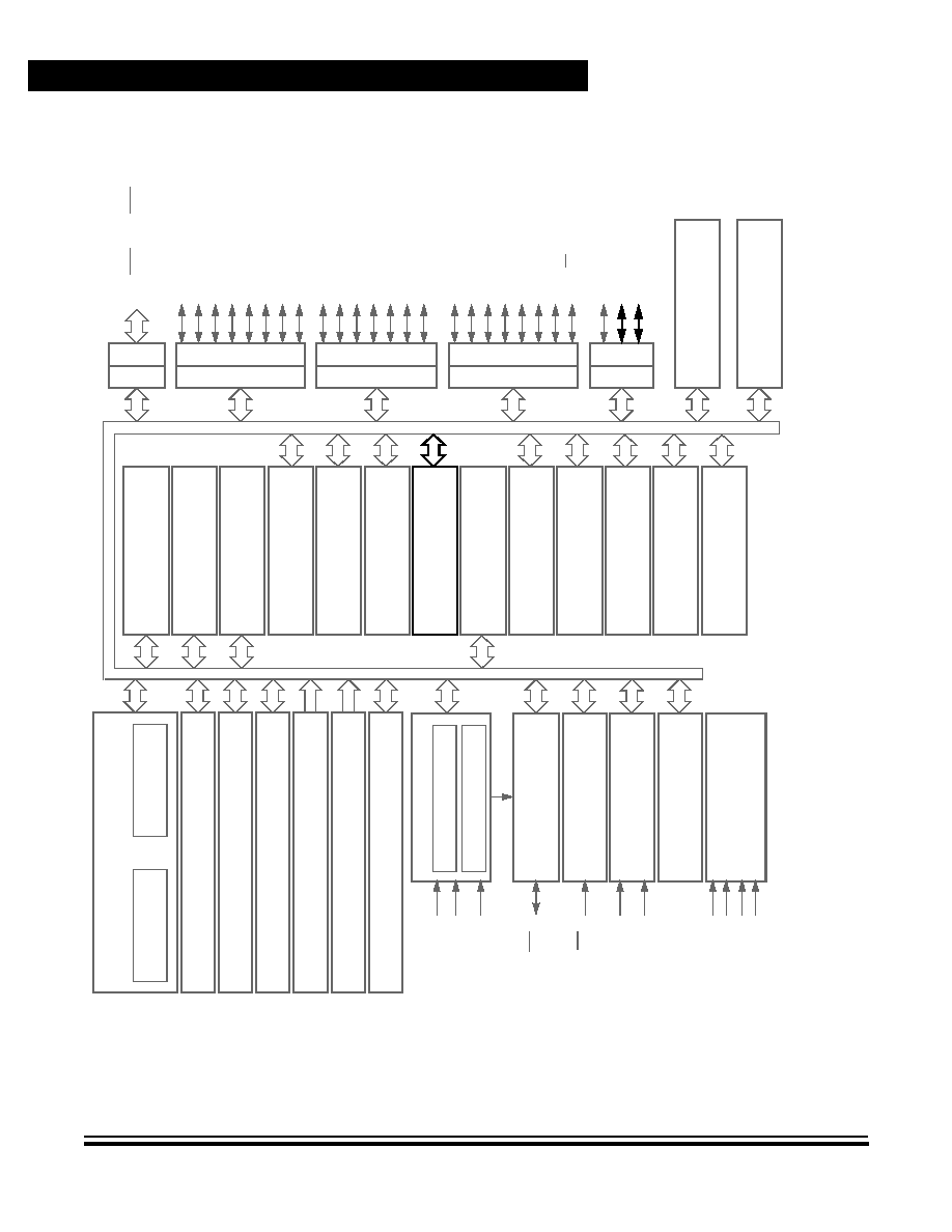
Data Sheet
MC6
8
HC90
8
GR16 --
Re
v. 1.0
160
Enha
nced Seria
l
C
o
mmu
n
icatio
ns
Interface (ESCI) Modu
le
MOTOROLA
Enhanced Serial Comm
uni
cations Interface (ESCI)
Figure 14-1. Block Diagram Highlighting ESCI Block and Pins
MONITOR MODULE
M68HC08 CPU
CONTROL AND STATUS REGISTERS -- 64 BYTES
USER FLASH -- 15,872 BYTES
USER RAM -- 1024 BYTES
MONITOR ROM -- 350 BYTES
USER FLASH VECTOR SPACE -- 44 BYTES
PORTA
D
DRA
DDRC
PO
R
T
C
DDR
D
PORTD
DDRE
POR
T
E
INTERNAL BUS
OSC1
OSC2
RST
(3)
IRQ
(3)
PTA7/KBD7�PTA0/KBD0
(1)
PTB7/AD7
PTB6/AD6
PTB5/AD5
PTB4/AD4
PTB3/AD3
PTB2/AD2
PTB1/AD1
PTB0/AD0
PTC6
(1)
PTC5
(1)
PTC4
(1), (2)
PTC3
(1), (2)
PTC2
(1), (2)
PTC1
(1), (2)
PTC0
(1), (2)
PTD7/T2CH1
(1)
PTD6/T2CH0
(1)
PTD5/T1CH1
(1)
PTD4/T1CH0
(1)
PTD3/SPSCK
(1)
PTD2/MOSI
(1)
PTD1/MISO
(1)
PTD0/SS
(1)
PTE1/RxD
PTE0/TxD
SECURITY
MODULE
POWER
V
SS
V
DD
V
SSA
V
DDA
1. Ports are software configurable with pullup device if input port.
2. Higher current drive port pins
3. Pin contains integrated pullup device
MONITOR MODE ENTRY
MODULE
DDRB
PORTB
V
DDAD
/V
REFH
V
DDAD
/V
REFL
PTE5�PTE2
FLASH PROGRAMMING ROUTINES ROM -- 406 BYTES
CLOCK GENERATOR MODULE
CGMXFC
PHASE LOCKED LOOP
32�100 kHz OSCILLATOR
CPU
REGISTERS
ARITHMETIC/LOGIC
UNIT (ALU)
SYSTEM INTEGRATION
MODULE
SINGLE EXTERNAL
INTERRUPT MODULE
10-BIT ANALOG-TO-DIGITAL
CONVERTER MODULE
POWER-ON RESET
MODULE
PROGRAMMABLE TIMEBASE
MODULE
SINGLE BREAKPOINT
BREAK MODULE
DUAL VOLTAGE
LOW-VOLTAGE INHIBIT
MODULE
8-BIT KEYBOARD
INTERRUPT MODULE
2-CHANNEL TIMER
INTERFACE MODULE 1
2-CHANNEL TIMER
INTERFACE MODULE 2
ENHANCED SERIAL
COMUNICATIONS
INTERFACE MODULE
COMPUTER OPERATING
PROPERLY MODULE
SERIAL PERIPHERAL
INTERFACE MODULE
DATA BUS SWITCH
MODULE
MEMORY MAP
MODULE
CONFIGURATION
REGISTER 1�2
MODULE

Enhanced Serial Communications Interface (ESCI) Module
Pin Name Conventions
MC68HC908GR16 -- Rev. 1.0
Data Sheet
MOTOROLA
Enhanced Serial Communications Interface (ESCI) Module
161
14.3 Pin Name Conventions
The generic names of the ESCI input/output (I/O) pins are:
�
RxD (receive data)
�
TxD (transmit data)
ESCI I/O lines are implemented by sharing parallel I/O port pins. The full name of
an ESCI input or output reflects the name of the shared port pin.
Table 14-1
shows
the full names and the generic names of the ESCI I/O pins. The generic pin names
appear in the text of this section.
14.4 Functional Description
Figure 14-2
shows the structure of the ESCI module. The ESCI allows full-duplex,
asynchronous, NRZ serial communication between the MCU and remote devices,
including other MCUs. The transmitter and receiver of the ESCI operate
independently, although they use the same baud rate generator. During normal
operation, the CPU monitors the status of the ESCI, writes the data to be
transmitted, and processes received data.
The baud rate clock source for the ESCI can be selected via the configuration bit,
SCIBDSRC, of the CONFIG2 register ($001E).
For reference, a summary of the ESCI module input/output registers is provided in
Figure 14-3
.
Table 14-1. Pin Name Conventions
Generic Pin Names
RxD
TxD
Full Pin Names
PTE1/RxD
PTE0/TxD
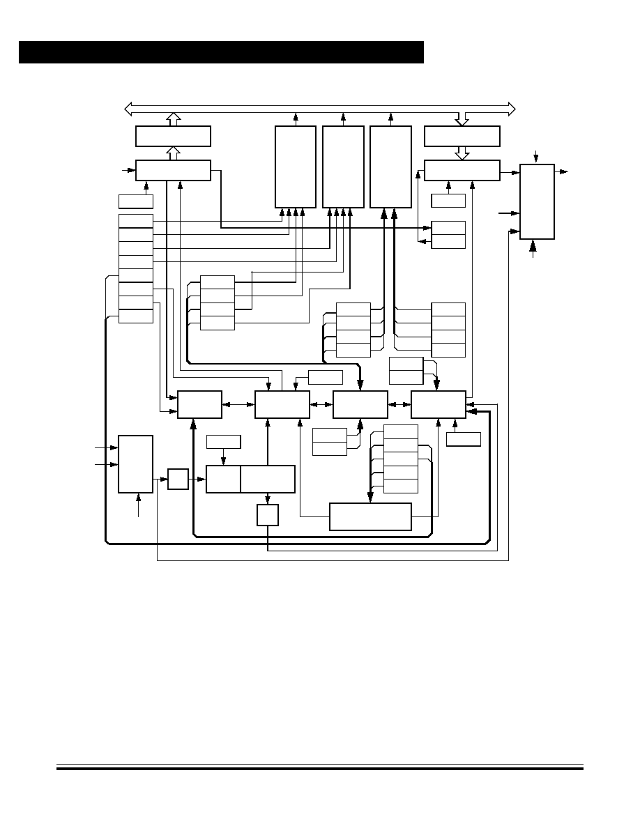
Enhanced Serial Communications Interface (ESCI) Module
Data Sheet
MC68HC908GR16 -- Rev. 1.0
162
Enhanced Serial Communications Interface (ESCI) Module
MOTOROLA
Figure 14-2. ESCI Module Block Diagram
SCTE
TC
SCRF
IDLE
OR
NF
FE
PE
SCTIE
TCIE
SCRIE
ILIE
TE
RE
RWU
SBK
R8
T8
ORIE
FEIE
PEIE
BKF
RPF
ESCI DATA
RECEIVE
SHIFT REGISTER
ESCI DATA
REGISTER
TRANSMIT
SHIFT REGISTER
NEIE
M
WAKE
ILTY
FLAG
CONTROL
TRANSMIT
CONTROL
RECEIVE
CONTROL
DATA SELECTION
CONTROL
WAKEUP
PTY
PEN
REGISTER
TRANSMITTER
INT
ERRUPT
CONT
ROL
RE
CEIVE
R
INT
ERRUPT
CONT
ROL
ERR
OR
INT
ERRUPT
CONT
ROL
CONTROL
ENSCI
LOOPS
ENSCI
INTERNAL BUS
TXINV
LOOPS
� 4
� 16
PRE-
SCALER
BAUD RATE
GENERATOR
BUS CLOCK
RxD
TxD
ARBITER-
SCI_TxD
RxD
LINR
LINT
CGMXCLK
ESCIBDSRC
FR
O
M
CONFIG2
SL
SL=1 -> SCI_CLK = BUSCLK
SL=0 -> SCI_CLK = CGMXCLK (4x BUSCLK)
SCI
_CLK
BUS_CLK
ACLK BIT IN SCIACTL
SL
E
NHANCED
PRESCAL
ER
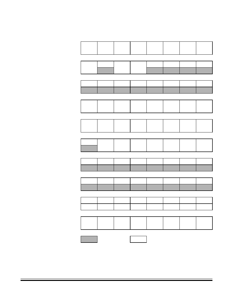
Enhanced Serial Communications Interface (ESCI) Module
Functional Description
MC68HC908GR16 -- Rev. 1.0
Data Sheet
MOTOROLA
Enhanced Serial Communications Interface (ESCI) Module
163
Addr.
Register Name
Bit 7
6
5
4
3
2
1
Bit 0
$0009
ESCI Prescaler Register
(SCPSC)
See page 187.
Read:
PDS2
PDS1
PDS0
PSSB4
PSSB3
PSSB2
PSSB1
PSSB0
Write:
Reset:
0
0
0
0
0
0
0
0
$000A
ESCI Arbiter Control
Register (SCIACTL)
See page 191.
Read:
AM1
ALOST
AM0
ACLK
AFIN
ARUN
AROVFL
ARD8
Write:
Reset:
0
0
0
0
0
0
0
0
$000B
ESCI Arbiter Data
Register (SCIADAT)
See page 192.
Read:
ARD7
ARD6
ARD5
ARD4
ARD3
ARD2
ARD1
ARD0
Write:
Reset:
0
0
0
0
0
0
0
0
$0013
ESCI Control Register 1
(SCC1)
See page 176.
Read:
LOOPS
ENSCI
TXINV
M
WAKE
ILTY
PEN
PTY
Write:
Reset:
0
0
0
0
0
0
0
0
$0014
ESCI Control Register 2
(SCC2)
See page 178.
Read:
SCTIE
TCIE
SCRIE
ILIE
TE
RE
RWU
SBK
Write:
Reset:
0
0
0
0
0
0
0
0
$0015
ESCI Control Register 3
(SCC3)
See page 180.
Read:
R8
T8
R
R
ORIE
NEIE
FEIE
PEIE
Write:
Reset:
U
0
0
0
0
0
0
0
$0016
ESCI Status Register 1
(SCS1)
See page 181.
Read:
SCTE
TC
SCRF
IDLE
OR
NF
FE
PE
Write:
Reset:
1
1
0
0
0
0
0
0
$0017
ESCI Status Register 2
(SCS2)
See page 184.
Read:
0
0
0
0
0
0
BKF
RPF
Write:
Reset:
0
0
0
0
0
0
0
0
$0018
ESCI Data Register
(SCDR)
See page 185.
Read:
R7
R6
R5
R4
R3
R2
R1
R0
Write:
T7
T6
T5
T4
T3
T2
T1
T0
Reset:
Unaffected by reset
$0019
ESCI Baud Rate Register
(SCBR)
See page 185.
Read:
LINT
LINR
SCP1
SCP0
R
SCR2
SCR1
SCR0
Write:
Reset:
0
0
0
0
0
0
0
0
= Unimplemented
R
= Reserved
Figure 14-3. ESCI I/O Register Summary

Enhanced Serial Communications Interface (ESCI) Module
Data Sheet
MC68HC908GR16 -- Rev. 1.0
164
Enhanced Serial Communications Interface (ESCI) Module
MOTOROLA
14.4.1 Data Format
The SCI uses the standard non-return-to-zero mark/space data format illustrated
in
Figure 14-4
.
Figure 14-4. SCI Data Formats
14.4.2 Transmitter
Figure 14-5
shows the structure of the SCI transmitter and the registers are
summarized in
Figure 14-3
. The baud rate clock source for the ESCI can be
selected via the configuration bit, SCIBDSRC.
14.4.2.1 Character Length
The transmitter can accommodate either 8-bit or 9-bit data. The state of the M bit
in ESCI control register 1 (SCC1) determines character length. When transmitting
9-bit data, bit T8 in ESCI control register 3 (SCC3) is the ninth bit (bit 8).
14.4.2.2 Character Transmission
During an ESCI transmission, the transmit shift register shifts a character out to the
TxD pin. The ESCI data register (SCDR) is the write-only buffer between the
internal data bus and the transmit shift register.
To initiate an ESCI transmission:
1.
Enable the ESCI by writing a logic 1 to the enable ESCI bit (ENSCI) in ESCI
control register 1 (SCC1).
2.
Enable the transmitter by writing a logic 1 to the transmitter enable bit (TE)
in ESCI control register 2 (SCC2).
3.
Clear the ESCI transmitter empty bit (SCTE) by first reading ESCI status
register 1 (SCS1) and then writing to the SCDR. For 9-bit data, also write the
T8 bit in SCC3.
4.
Repeat step 3 for each subsequent transmission.
BIT 5
BIT 0
BIT 1
BIT 0
BIT 1
BIT 2
BIT 3
BIT 4
BIT 5
BIT 6
BIT 7
BIT 8
BIT 2
BIT 3
BIT 4
BIT 6
BIT 7
PARITY
OR DATA
BIT
PARITY
OR DATA
BIT
NEXT
START
BIT
NEXT
START
BIT
STOP
BIT
STOP
BIT
8-BIT DATA FORMAT
(BIT M IN SCC1 CLEAR)
9-BIT DATA FORMAT
(BIT M IN SCC1 SET)
START
BIT
START
BIT
Enhanced Serial Communications Interface (ESCI) Module
Functional Description
MC68HC908GR16 -- Rev. 1.0
Data Sheet
MOTOROLA
Enhanced Serial Communications Interface (ESCI) Module
165
Figure 14-5. ESCI Transmitter
At the start of a transmission, transmitter control logic automatically loads the
transmit shift register with a preamble of logic 1s. After the preamble shifts out,
control logic transfers the SCDR data into the transmit shift register. A logic 0 start
bit automatically goes into the least significant bit (LSB) position of the transmit shift
register. A logic 1 stop bit goes into the most significant bit (MSB) position.
The ESCI transmitter empty bit, SCTE, in SCS1 becomes set when the SCDR
transfers a byte to the transmit shift register. The SCTE bit indicates that the SCDR
can accept new data from the internal data bus. If the ESCI transmit interrupt
enable bit, SCTIE, in SCC2 is also set, the SCTE bit generates a transmitter CPU
interrupt request.
When the transmit shift register is not transmitting a character, the TxD pin goes to
the idle condition, logic 1. If at any time software clears the ENSCI bit in ESCI
control register 1 (SCC1), the transmitter and receiver relinquish control of the
port E pins.
PEN
PTY
H
8
7
6
5
4
3
2
1
0
L
11-BIT
TRANSMIT
STOP
START
T8
SCTE
SCTIE
TCIE
SBK
TC
BUS C
L
OCK
PARITY
GENERATION
MSB
ESCI DATA REGISTER
LOAD FROM SCDR
SHIFT ENABLE
PREAMBLE
(A
LL ONES)
BREAK
(
A
LL
ZE
ROS)
TRANSMITTER
CONTROL LOGIC
SHIFT REGISTER
TC
SCTIE
TCIE
SCTE
TRANSMITTER
CPU
I
N
T
E
R
R
U
P
T
R
E
Q
U
E
S
T
M
ENSCI
LOOPS
TE
TXINV
INTERNAL BUS
�
4
PRE-
SCALER
SCP1
SCP0
SCR2
SCR1
SCR0
BAUD
DIVIDER
�
16
SCI_TxD
PRE-
SCALE
R
PDS1
PDS2
PDS0
PSSB3
PSSB4
PSSB2
PSSB1
PSSB0
LINT

Enhanced Serial Communications Interface (ESCI) Module
Data Sheet
MC68HC908GR16 -- Rev. 1.0
166
Enhanced Serial Communications Interface (ESCI) Module
MOTOROLA
14.4.2.3 Break Characters
Writing a logic 1 to the send break bit, SBK, in SCC2 loads the transmit shift
register with a break character. For TXINV = 0 (output not inverted), a transmitted
break character contains all logic 0s and has no start, stop, or parity bit. Break
character length depends on the M bit in SCC1 and the LINR bits in SCBR. As long
as SBK is at logic 1, transmitter logic continuously loads break characters into the
transmit shift register. After software clears the SBK bit, the shift register finishes
transmitting the last break character and then transmits at least one logic 1. The
automatic logic 1 at the end of a break character guarantees the recognition of the
start bit of the next character.
When LINR is cleared in SCBR, the ESCI recognizes a break character when a
start bit is followed by eight or nine logic 0 data bits and a logic 0 where the stop bit
should be, resulting in a total of 10 or 11 consecutive logic 0 data bits. When LINR
is set in SCBR, the ESCI recognizes a break character when a start bit is followed
by 9 or 10 logic 0 data bits and a logic 0 where the stop bit should be, resulting in
a total of 11 or 12 consecutive logic 0 data bits.
Receiving a break character has these effects on ESCI registers:
�
Sets the framing error bit (FE) in SCS1
�
Sets the ESCI receiver full bit (SCRF) in SCS1
�
Clears the ESCI data register (SCDR)
�
Clears the R8 bit in SCC3
�
Sets the break flag bit (BKF) in SCS2
�
May set the overrun (OR), noise flag (NF), parity error (PE),
or reception in progress flag (RPF) bits
14.4.2.4 Idle Characters
For TXINV = 0 (output not inverted), a transmitted idle character contains all logic
1s and has no start, stop, or parity bit. Idle character length depends on the M bit
in SCC1. The preamble is a synchronizing idle character that begins every
transmission.
If the TE bit is cleared during a transmission, the TxD pin becomes idle after
completion of the transmission in progress. Clearing and then setting the TE bit
during a transmission queues an idle character to be sent after the character
currently being transmitted.
NOTE:
When a break sequence is followed immediately by an idle character, this SCI
design exhibits a condition in which the break character length is reduced by one
half bit time. In this instance, the break sequence will consist of a valid start bit,
eight or nine data bits (as defined by the M bit in SCC1) of logic 0 and one half data
bit length of logic 0 in the stop bit position followed immediately by the idle
character. To ensure a break character of the proper length is transmitted, always
queue up a byte of data to be transmitted while the final break sequence is in
progress.

Enhanced Serial Communications Interface (ESCI) Module
Functional Description
MC68HC908GR16 -- Rev. 1.0
Data Sheet
MOTOROLA
Enhanced Serial Communications Interface (ESCI) Module
167
When queueing an idle character, return the TE bit to logic 1 before the stop bit of
the current character shifts out to the TxD pin. Setting TE after the stop bit appears
on TxD causes data previously written to the SCDR to be lost. A good time to toggle
the TE bit for a queued idle character is when the SCTE bit becomes set and just
before writing the next byte to the SCDR.
14.4.2.5 Inversion of Transmitted Output
The transmit inversion bit (TXINV) in ESCI control register 1 (SCC1) reverses
the polarity of transmitted data. All transmitted values including idle, break, start,
and stop bits, are inverted when TXINV is at logic 1. See
14.8.1 ESCI Control
Register 1
.
14.4.2.6 Transmitter Interrupts
These conditions can generate CPU interrupt requests from the ESCI transmitter:
�
ESCI transmitter empty (SCTE) -- The SCTE bit in SCS1 indicates that the
SCDR has transferred a character to the transmit shift register. SCTE can
generate a transmitter CPU interrupt request. Setting the ESCI transmit
interrupt enable bit, SCTIE, in SCC2 enables the SCTE bit to generate
transmitter CPU interrupt requests.
�
Transmission complete (TC) -- The TC bit in SCS1 indicates that the
transmit shift register and the SCDR are empty and that no break or idle
character has been generated. The transmission complete interrupt enable
bit, TCIE, in SCC2 enables the TC bit to generate transmitter CPU interrupt
requests.
14.4.3 Receiver
Figure 14-6
shows the structure of the ESCI receiver. The receiver I/O registers
are summarized in
Figure 14-3
.
14.4.3.1 Character Length
The receiver can accommodate either 8-bit or 9-bit data. The state of the M bit in
ESCI control register 1 (SCC1) determines character length. When receiving 9-bit
data, bit R8 in ESCI control register 3 (SCC3) is the ninth bit (bit 8). When receiving
8-bit data, bit R8 is a copy of the eighth bit (bit 7).
Enhanced Serial Communications Interface (ESCI) Module
Data Sheet
MC68HC908GR16 -- Rev. 1.0
168
Enhanced Serial Communications Interface (ESCI) Module
MOTOROLA
Figure 14-6. ESCI Receiver Block Diagram
ALL
ONES
ALL ZEROS
M
WAKE
ILTY
PEN
PTY
BKF
RPF
H
8
7
6
5
4
3
2
1
0
L
11-BIT
RECEIVE SHIFT REGISTER
STOP
STAR
T
DATA
RECOVERY
OR
ORIE
NF
NEIE
FE
FEIE
PE
PEIE
SCRIE
SCRF
ILIE
IDLE
WAKEUP
LOGIC
PARITY
CHECKING
MSB
ERROR CPU
CP
U
INTERR
UPT
ESCI DATA REGISTER
R8
SCRIE
ILIE
RWU
SCRF
IDLE
INTERNAL BUS
PRE-
SCALER
BAUD
DIVIDER
�
4
�
16
SCP1
SCP0
SCR2
SCR1
SCR0
RxD
BUS
CLOC
K
PRE
-
SCAL
ER
PDS1
PDS2
PDS0
PSSB3
PSSB4
PSSB2
PSSB1
PSSB0
LINR
RE
QUEST
I
N
T
E
R
R
U
P
T
RE
QUEST
ORIE
NEIE
FEIE
PEIE
OR
NF
FE
PE
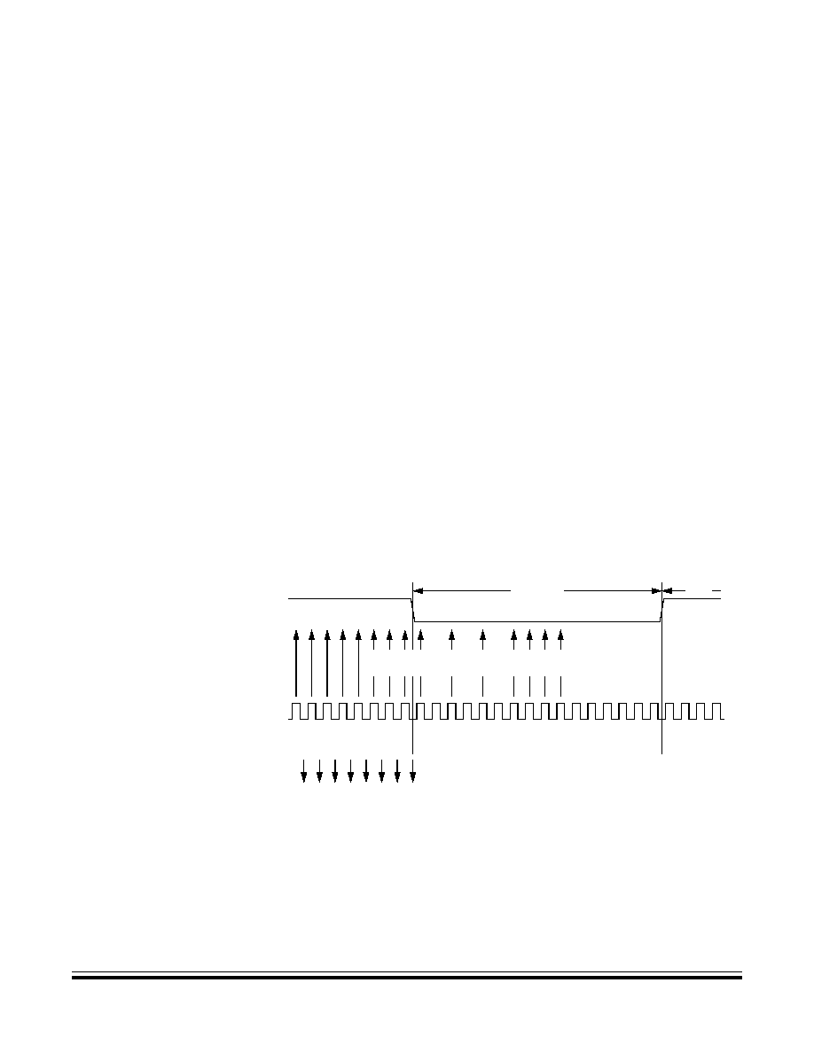
Enhanced Serial Communications Interface (ESCI) Module
Functional Description
MC68HC908GR16 -- Rev. 1.0
Data Sheet
MOTOROLA
Enhanced Serial Communications Interface (ESCI) Module
169
14.4.3.2 Character Reception
During an ESCI reception, the receive shift register shifts characters in from the
RxD pin. The ESCI data register (SCDR) is the read-only buffer between the
internal data bus and the receive shift register.
After a complete character shifts into the receive shift register, the data portion of
the character transfers to the SCDR. The ESCI receiver full bit, SCRF, in ESCI
status register 1 (SCS1) becomes set, indicating that the received byte can be
read. If the ESCI receive interrupt enable bit, SCRIE, in SCC2 is also set, the SCRF
bit generates a receiver CPU interrupt request.
14.4.3.3 Data Sampling
The receiver samples the RxD pin at the RT clock rate. The RT clock is an internal
signal with a frequency 16 times the baud rate. To adjust for baud rate mismatch,
the RT clock is resynchronized at these times (see
Figure 14-7
):
�
After every start bit
�
After the receiver detects a data bit change from logic 1 to logic 0 (after the
majority of data bit samples at RT8, RT9, and RT10 returns a valid logic 1
and the majority of the next RT8, RT9, and RT10 samples returns a valid
logic 0)
To locate the start bit, data recovery logic does an asynchronous search for a
logic 0 preceded by three logic 1s. When the falling edge of a possible start bit
occurs, the RT clock begins to count to 16.
Figure 14-7. Receiver Data Sampling
To verify the start bit and to detect noise, data recovery logic takes samples at RT3,
RT5, and RT7.
Table 14-2
summarizes the results of the start bit verification
samples.
RT CLOCK
RESET
RT1
RT1
RT1
RT1
RT1
RT1
RT1
RT1
RT1
RT2
RT3
RT4
RT5
RT8
RT7
RT6
RT1
1
RT1
0
RT9
RT1
5
RT1
4
RT1
3
RT1
2
RT1
6
RT1
RT2
RT3
RT4
START BIT
QUALIFICATION
START BIT
VERIFICATION
DATA
SAMPLING
SAMPLES
RT
CLOCK
RT CLOCK
STATE
START BIT
LSB
RxD
Enhanced Serial Communications Interface (ESCI) Module
Data Sheet
MC68HC908GR16 -- Rev. 1.0
170
Enhanced Serial Communications Interface (ESCI) Module
MOTOROLA
If start bit verification is not successful, the RT clock is reset and a new search for
a start bit begins.
To determine the value of a data bit and to detect noise, recovery logic takes
samples at RT8, RT9, and RT10.
Table 14-3
summarizes the results of the data
bit samples.
NOTE:
The RT8, RT9, and RT10 samples do not affect start bit verification. If any or all of
the RT8, RT9, and RT10 start bit samples are logic 1s following a successful start
bit verification, the noise flag (NF) is set and the receiver assumes that the bit is a
start bit.
To verify a stop bit and to detect noise, recovery logic takes samples at RT8, RT9,
and RT10.
Table 14-4
summarizes the results of the stop bit samples.
Table 14-2. Start Bit Verification
RT3, RT5, and RT7 Samples
Start Bit Verification
Noise Flag
000
Yes
0
001
Yes
1
010
Yes
1
011
No
0
100
Yes
1
101
No
0
110
No
0
111
No
0
Table 14-3. Data Bit Recovery
RT8, RT9, and RT10 Samples
Data Bit Determination
Noise Flag
000
0
0
001
0
1
010
0
1
011
1
1
100
0
1
101
1
1
110
1
1
111
1
0
Table 14-4. Stop Bit Recovery
RT8, RT9, and RT10 Samples
Framing Error Flag
Noise Flag
000
1
0
001
1
1
010
1
1
011
0
1
100
1
1
101
0
1
110
0
1
111
0
0
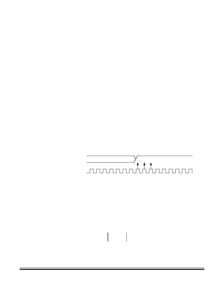
Enhanced Serial Communications Interface (ESCI) Module
Functional Description
MC68HC908GR16 -- Rev. 1.0
Data Sheet
MOTOROLA
Enhanced Serial Communications Interface (ESCI) Module
171
14.4.3.4 Framing Errors
If the data recovery logic does not detect a logic 1 where the stop bit should be in
an incoming character, it sets the framing error bit, FE, in SCS1. A break character
also sets the FE bit because a break character has no stop bit. The FE bit is set at
the same time that the SCRF bit is set.
14.4.3.5 Baud Rate Tolerance
A transmitting device may be operating at a baud rate below or above the receiver
baud rate. Accumulated bit time misalignment can cause one of the three stop bit
data samples to fall outside the actual stop bit. Then a noise error occurs. If more
than one of the samples is outside the stop bit, a framing error occurs. In most
applications, the baud rate tolerance is much more than the degree of
misalignment that is likely to occur.
As the receiver samples an incoming character, it resynchronizes the RT clock on
any valid falling edge within the character. Resynchronization within characters
corrects misalignments between transmitter bit times and receiver bit times.
Slow Data Tolerance
Figure 14-8
shows how much a slow received character can be misaligned
without causing a noise error or a framing error. The slow stop bit begins at RT8
instead of RT1 but arrives in time for the stop bit data samples at RT8, RT9, and
RT10.
Figure 14-8. Slow Data
For an 8-bit character, data sampling of the stop bit takes the receiver
9 bit times
�
16 RT cycles + 10 RT cycles = 154 RT cycles.
With the misaligned character shown in
Figure 14-8
, the receiver counts 154
RT cycles at the point when the count of the transmitting device is 9 bit
times
�
16 RT cycles + 3 RT cycles = 147 RT cycles.
The maximum percent difference between the receiver count and the
transmitter count of a slow 8-bit character with no errors is:
For a 9-bit character, data sampling of the stop bit takes the receiver
10 bit times
�
16 RT cycles + 10 RT cycles = 170 RT cycles.
MSB
STOP
RT1
RT2
RT3
RT4
RT5
RT6
RT7
RT8
RT9
RT10
RT11
RT12
RT13
RT14
RT15
RT16
DATA
SAMPLES
RECEIVER
RT CLOCK
154
147
�
154
--------------------------
100
�
4.54%
=
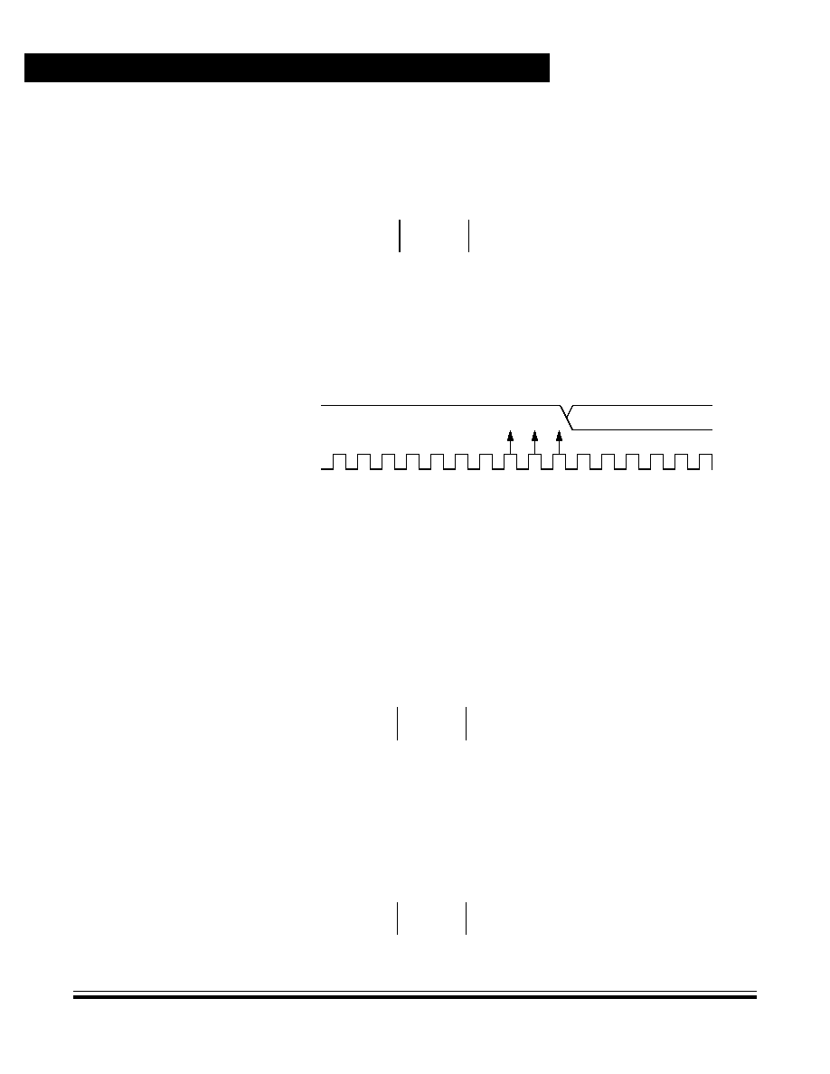
Enhanced Serial Communications Interface (ESCI) Module
Data Sheet
MC68HC908GR16 -- Rev. 1.0
172
Enhanced Serial Communications Interface (ESCI) Module
MOTOROLA
With the misaligned character shown in
Figure 14-8
, the receiver counts 170
RT cycles at the point when the count of the transmitting device is 10 bit
times
�
16 RT cycles + 3 RT cycles = 163 RT cycles.
The maximum percent difference between the receiver count and the
transmitter count of a slow 9-bit character with no errors is:
Fast Data Tolerance
Figure 14-9
shows how much a fast received character can be misaligned
without causing a noise error or a framing error. The fast stop bit ends at RT10
instead of RT16 but is still there for the stop bit data samples at RT8, RT9, and
RT10.
Figure 14-9. Fast Data
For an 8-bit character, data sampling of the stop bit takes the receiver
9 bit times
�
16 RT cycles + 10 RT cycles = 154 RT cycles.
With the misaligned character shown in
Figure 14-9
, the receiver counts 154
RT cycles at the point when the count of the transmitting device is
10 bit times
�
16 RT cycles = 160 RT cycles.
The maximum percent difference between the receiver count and the
transmitter count of a fast 8-bit character with no errors is
For a 9-bit character, data sampling of the stop bit takes the receiver
10 bit times
�
16 RT cycles + 10 RT cycles = 170 RT cycles.
With the misaligned character shown in
Figure 14-9
, the receiver counts 170
RT cycles at the point when the count of the transmitting device is
11 bit times
�
16 RT cycles = 176 RT cycles.
The maximum percent difference between the receiver count and the
transmitter count of a fast 9-bit character with no errors is:
170
163
�
170
--------------------------
100
�
4.12%
=
IDLE OR NEXT CHARACTER
STOP
RT
1
RT
2
RT
3
RT
4
RT
5
RT
6
RT
7
RT
8
RT
9
RT
10
RT
11
RT
12
RT
13
RT
14
RT
15
RT
16
DATA
SAMPLES
RECEIVER
RT CLOCK
154
160
�
154
--------------------------
100
�
3.90%.
=
170
176
�
170
--------------------------
100
�
3.53%.
=

Enhanced Serial Communications Interface (ESCI) Module
Functional Description
MC68HC908GR16 -- Rev. 1.0
Data Sheet
MOTOROLA
Enhanced Serial Communications Interface (ESCI) Module
173
14.4.3.6 Receiver Wakeup
So that the MCU can ignore transmissions intended only for other receivers in
multiple-receiver systems, the receiver can be put into a standby state. Setting the
receiver wakeup bit, RWU, in SCC2 puts the receiver into a standby state during
which receiver interrupts are disabled.
Depending on the state of the WAKE bit in SCC1, either of two conditions on the
RxD pin can bring the receiver out of the standby state:
1.
Address mark -- An address mark is a logic 1 in the MSB position of a
received character. When the WAKE bit is set, an address mark wakes the
receiver from the standby state by clearing the RWU bit. The address mark
also sets the ESCI receiver full bit, SCRF. Software can then compare the
character containing the address mark to the user-defined address of the
receiver. If they are the same, the receiver remains awake and processes
the characters that follow. If they are not the same, software can set the
RWU bit and put the receiver back into the standby state.
2.
Idle input line condition -- When the WAKE bit is clear, an idle character on
the RxD pin wakes the receiver from the standby state by clearing the RWU
bit. The idle character that wakes the receiver does not set the receiver idle
bit, IDLE, or the ESCI receiver full bit, SCRF. The idle line type bit, ILTY,
determines whether the receiver begins counting logic 1s as idle character
bits after the start bit or after the stop bit.
NOTE:
With the WAKE bit clear, setting the RWU bit after the RxD pin has been idle will
cause the receiver to wakeup.
14.4.3.7 Receiver Interrupts
These sources can generate CPU interrupt requests from the ESCI receiver:
�
ESCI receiver full (SCRF) -- The SCRF bit in SCS1 indicates that the
receive shift register has transferred a character to the SCDR. SCRF can
generate a receiver CPU interrupt request. Setting the ESCI receive
interrupt enable bit, SCRIE, in SCC2 enables the SCRF bit to generate
receiver CPU interrupts.
�
Idle input (IDLE) -- The IDLE bit in SCS1 indicates that 10 or 11 consecutive
logic 1s shifted in from the RxD pin. The idle line interrupt enable bit, ILIE,
in SCC2 enables the IDLE bit to generate CPU interrupt requests.
14.4.3.8 Error Interrupts
These receiver error flags in SCS1 can generate CPU interrupt requests:
�
Receiver overrun (OR) -- The OR bit indicates that the receive shift register
shifted in a new character before the previous character was read from the
SCDR. The previous character remains in the SCDR, and the new character
is lost. The overrun interrupt enable bit, ORIE, in SCC3 enables OR to
generate ESCI error CPU interrupt requests.

Enhanced Serial Communications Interface (ESCI) Module
Data Sheet
MC68HC908GR16 -- Rev. 1.0
174
Enhanced Serial Communications Interface (ESCI) Module
MOTOROLA
�
Noise flag (NF) -- The NF bit is set when the ESCI detects noise on
incoming data or break characters, including start, data, and stop bits. The
noise error interrupt enable bit, NEIE, in SCC3 enables NF to generate ESCI
error CPU interrupt requests.
�
Framing error (FE) -- The FE bit in SCS1 is set when a logic 0 occurs where
the receiver expects a stop bit. The framing error interrupt enable bit, FEIE,
in SCC3 enables FE to generate ESCI error CPU interrupt requests.
�
Parity error (PE) -- The PE bit in SCS1 is set when the ESCI detects a parity
error in incoming data. The parity error interrupt enable bit, PEIE, in SCC3
enables PE to generate ESCI error CPU interrupt requests.
14.5 Low-Power Modes
The WAIT and STOP instructions put the MCU in low power-consumption standby
modes.
14.5.1 Wait Mode
The ESCI module remains active in wait mode. Any enabled CPU interrupt request
from the ESCI module can bring the MCU out of wait mode.
If ESCI module functions are not required during wait mode, reduce power
consumption by disabling the module before executing the WAIT instruction.
14.5.2 Stop Mode
The ESCI module is inactive in stop mode. The STOP instruction does not affect
ESCI register states. ESCI module operation resumes after the MCU exits stop
mode.
Because the internal clock is inactive during stop mode, entering stop mode during
an ESCI transmission or reception results in invalid data.
14.6 ESCI During Break Module Interrupts
The BCFE bit in the break flag control register (SBFCR) enables software to clear
status bits during the break state. See
Section 19. Development Support
.
To allow software to clear status bits during a break interrupt, write a logic 1 to the
BCFE bit. If a status bit is cleared during the break state, it remains cleared when
the MCU exits the break state.
To protect status bits during the break state, write a logic 0 to the BCFE bit. With
BCFE at logic 0 (its default state), software can read and write I/O registers during
the break state without affecting status bits. Some status bits have a two-step
read/write clearing procedure. If software does the first step on such a bit before

Enhanced Serial Communications Interface (ESCI) Module
I/O Signals
MC68HC908GR16 -- Rev. 1.0
Data Sheet
MOTOROLA
Enhanced Serial Communications Interface (ESCI) Module
175
the break, the bit cannot change during the break state as long as BCFE is at
logic 0. After the break, doing the second step clears the status bit.
14.7 I/O Signals
Port E shares two of its pins with the ESCI module. The two ESCI I/O pins are:
�
PTE0/TxD -- transmit data
�
PTE1/RxD -- receive data
14.7.1 PTE0/TxD (Transmit Data)
The PTE0/TxD pin is the serial data output from the ESCI transmitter. The ESCI
shares the PTE0/TxD pin with port E. When the ESCI is enabled, the PTE0/TxD
pin is an output regardless of the state of the DDRE0 bit in data direction register
E (DDRE).
14.7.2 PTE1/RxD (Receive Data)
The PTE1/RxD pin is the serial data input to the ESCI receiver. The ESCI shares
the PTE1/RxD pin with port E. When the ESCI is enabled, the PTE1/RxD pin is an
input regardless of the state of the DDRE1 bit in data direction register E (DDRE).
14.8 I/O Registers
These I/O registers control and monitor ESCI operation:
�
ESCI control register 1, SCC1
�
ESCI control register 2, SCC2
�
ESCI control register 3, SCC3
�
ESCI status register 1, SCS1
�
ESCI status register 2, SCS2
�
ESCI data register, SCDR
�
ESCI baud rate register, SCBR
�
ESCI prescaler register, SCPSC
�
ESCI arbiter control register, SCIACTL
�
ESCI arbiter data register, SCIADAT
:

Enhanced Serial Communications Interface (ESCI) Module
Data Sheet
MC68HC908GR16 -- Rev. 1.0
176
Enhanced Serial Communications Interface (ESCI) Module
MOTOROLA
14.8.1 ESCI Control Register 1
ESCI control register 1 (SCC1):
�
Enables loop mode operation
�
Enables the ESCI
�
Controls output polarity
�
Controls character length
�
Controls ESCI wakeup method
�
Controls idle character detection
�
Enables parity function
�
Controls parity type
LOOPS -- Loop Mode Select Bit
This read/write bit enables loop mode operation. In loop mode the RxD pin is
disconnected from the ESCI, and the transmitter output goes into the receiver
input. Both the transmitter and the receiver must be enabled to use loop mode.
Reset clears the LOOPS bit.
1 = Loop mode enabled
0 = Normal operation enabled
ENSCI -- Enable ESCI Bit
This read/write bit enables the ESCI and the ESCI baud rate generator. Clearing
ENSCI sets the SCTE and TC bits in ESCI status register 1 and disables
transmitter interrupts. Reset clears the ENSCI bit.
1 = ESCI enabled
0 = ESCI disabled
TXINV -- Transmit Inversion Bit
This read/write bit reverses the polarity of transmitted data. Reset clears the
TXINV bit.
1 = Transmitter output inverted
0 = Transmitter output not inverted
NOTE:
Setting the TXINV bit inverts all transmitted values including idle, break, start, and
stop bits.
Address: $0013
Bit 7
6
5
4
3
2
1
Bit 0
Read:
LOOPS
ENSCI
TXINV
M
WAKE
ILTY
PEN
PTY
Write:
Reset:
0
0
0
0
0
0
0
0
Figure 14-10. ESCI Control Register 1 (SCC1)
Enhanced Serial Communications Interface (ESCI) Module
I/O Registers
MC68HC908GR16 -- Rev. 1.0
Data Sheet
MOTOROLA
Enhanced Serial Communications Interface (ESCI) Module
177
M -- Mode (Character Length) Bit
This read/write bit determines whether ESCI characters are eight or nine bits
long (See
Table 14-5
).The ninth bit can serve as a receiver wakeup signal or as
a parity bit. Reset clears the M bit.
1 = 9-bit ESCI characters
0 = 8-bit ESCI characters
WAKE -- Wakeup Condition Bit
This read/write bit determines which condition wakes up the ESCI: a logic 1
(address mark) in the MSB position of a received character or an idle condition
on the RxD pin. Reset clears the WAKE bit.
1 = Address mark wakeup
0 = Idle line wakeup
ILTY -- Idle Line Type Bit
This read/write bit determines when the ESCI starts counting logic 1s as idle
character bits. The counting begins either after the start bit or after the stop bit.
If the count begins after the start bit, then a string of logic 1s preceding the stop
bit may cause false recognition of an idle character. Beginning the count after
the stop bit avoids false idle character recognition, but requires properly
synchronized transmissions. Reset clears the ILTY bit.
1 = Idle character bit count begins after stop bit
0 = Idle character bit count begins after start bit
PEN -- Parity Enable Bit
This read/write bit enables the ESCI parity function (see
Table 14-5
). When
enabled, the parity function inserts a parity bit in the MSB position (see
Table
14-3
). Reset clears the PEN bit.
1 = Parity function enabled
0 = Parity function disabled
PTY -- Parity Bit
This read/write bit determines whether the ESCI generates and checks for odd
parity or even parity (see
Table 14-5
). Reset clears the PTY bit.
1 = Odd parity
0 = Even parity
NOTE:
Changing the PTY bit in the middle of a transmission or reception can generate a
parity error.
Table 14-5. Character Format Selection
Control Bits
Character Format
M
PEN:PTY
Start Bits
Data Bits
Parity
Stop Bits
Character Length
0
0 X
1
8
None
1
10 bits
1
0 X
1
9
None
1
11 bits
0
1 0
1
7
Even
1
10 bits
0
1 1
1
7
Odd
1
10 bits
1
1 0
1
8
Even
1
11 bits
1
1 1
1
8
Odd
1
11 bits

Enhanced Serial Communications Interface (ESCI) Module
Data Sheet
MC68HC908GR16 -- Rev. 1.0
178
Enhanced Serial Communications Interface (ESCI) Module
MOTOROLA
14.8.2 ESCI Control Register 2
ESCI control register 2 (SCC2):
�
Enables these CPU interrupt requests:
�
SCTE bit to generate transmitter CPU interrupt requests
�
TC bit to generate transmitter CPU interrupt requests
�
SCRF bit to generate receiver CPU interrupt requests
�
IDLE bit to generate receiver CPU interrupt requests
�
Enables the transmitter
�
Enables the receiver
�
Enables ESCI wakeup
�
Transmits ESCI break characters
SCTIE -- ESCI Transmit Interrupt Enable Bit
This read/write bit enables the SCTE bit to generate ESCI transmitter CPU
interrupt requests. Setting the SCTIE bit in SCC2 enables the SCTE bit to
generate CPU interrupt requests. Reset clears the SCTIE bit.
1 = SCTE enabled to generate CPU interrupt
0 = SCTE not enabled to generate CPU interrupt
TCIE -- Transmission Complete Interrupt Enable Bit
This read/write bit enables the TC bit to generate ESCI transmitter CPU
interrupt requests. Reset clears the TCIE bit.
1 = TC enabled to generate CPU interrupt requests
0 = TC not enabled to generate CPU interrupt requests
SCRIE -- ESCI Receive Interrupt Enable Bit
This read/write bit enables the SCRF bit to generate ESCI receiver CPU
interrupt requests. Setting the SCRIE bit in SCC2 enables the SCRF bit to
generate CPU interrupt requests. Reset clears the SCRIE bit.
1 = SCRF enabled to generate CPU interrupt
0 = SCRF not enabled to generate CPU interrupt
ILIE -- Idle Line Interrupt Enable Bit
This read/write bit enables the IDLE bit to generate ESCI receiver CPU interrupt
requests. Reset clears the ILIE bit.
1 = IDLE enabled to generate CPU interrupt requests
0 = IDLE not enabled to generate CPU interrupt requests
Address: $0014
Bit 7
6
5
4
3
2
1
Bit 0
Read:
SCTIE
TCIE
SCRIE
ILIE
TE
RE
RWU
SBK
Write:
Reset:
0
0
0
0
0
0
0
0
Figure 14-11. ESCI Control Register 2 (SCC2)

Enhanced Serial Communications Interface (ESCI) Module
I/O Registers
MC68HC908GR16 -- Rev. 1.0
Data Sheet
MOTOROLA
Enhanced Serial Communications Interface (ESCI) Module
179
TE -- Transmitter Enable Bit
Setting this read/write bit begins the transmission by sending a preamble of 10
or 11 logic 1s from the transmit shift register to the TxD pin. If software clears
the TE bit, the transmitter completes any transmission in progress before the
TxD returns to the idle condition (logic 1). Clearing and then setting TE during a
transmission queues an idle character to be sent after the character currently
being transmitted. Reset clears the TE bit.
1 = Transmitter enabled
0 = Transmitter disabled
NOTE:
Writing to the TE bit is not allowed when the enable ESCI bit (ENSCI) is clear.
ENSCI is in ESCI control register 1.
RE -- Receiver Enable Bit
Setting this read/write bit enables the receiver. Clearing the RE bit disables the
receiver but does not affect receiver interrupt flag bits. Reset clears the RE bit.
1 = Receiver enabled
0 = Receiver disabled
NOTE:
Writing to the RE bit is not allowed when the enable ESCI bit (ENSCI) is clear.
ENSCI is in ESCI control register 1.
RWU -- Receiver Wakeup Bit
This read/write bit puts the receiver in a standby state during which receiver
interrupts are disabled. The WAKE bit in SCC1 determines whether an idle input
or an address mark brings the receiver out of the standby state and clears the
RWU bit. Reset clears the RWU bit.
1 = Standby state
0 = Normal operation
SBK -- Send Break Bit
Setting and then clearing this read/write bit transmits a break character followed
by a logic 1. The logic 1 after the break character guarantees recognition of a
valid start bit. If SBK remains set, the transmitter continuously transmits break
characters with no logic 1s between them. Reset clears the SBK bit.
1 = Transmit break characters
0 = No break characters being transmitted
NOTE:
Do not toggle the SBK bit immediately after setting the SCTE bit. Toggling SBK
before the preamble begins causes the ESCI to send a break character instead of
a preamble.
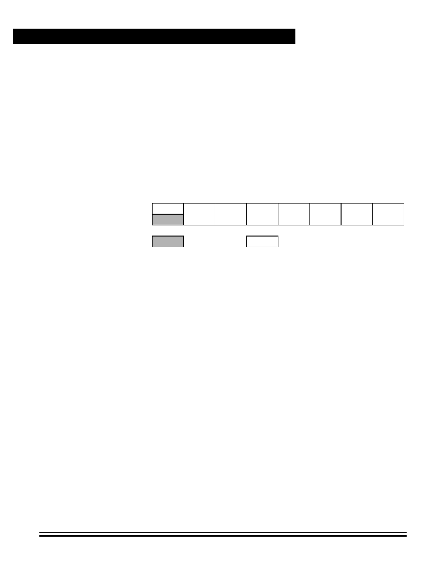
Enhanced Serial Communications Interface (ESCI) Module
Data Sheet
MC68HC908GR16 -- Rev. 1.0
180
Enhanced Serial Communications Interface (ESCI) Module
MOTOROLA
14.8.3 ESCI Control Register 3
ESCI control register 3 (SCC3):
�
Stores the ninth ESCI data bit received and the ninth ESCI data bit to be
transmitted.
�
Enables these interrupts:
�
Receiver overrun
�
Noise error
�
Framing error
�
Parity error
R8 -- Received Bit 8
When the ESCI is receiving 9-bit characters, R8 is the read-only ninth bit (bit 8)
of the received character. R8 is received at the same time that the SCDR
receives the other 8 bits.
When the ESCI is receiving 8-bit characters, R8 is a copy of the eighth bit (bit
7). Reset has no effect on the R8 bit.
T8 -- Transmitted Bit 8
When the ESCI is transmitting 9-bit characters, T8 is the read/write ninth bit
(bit 8) of the transmitted character. T8 is loaded into the transmit shift register at
the same time that the SCDR is loaded into the transmit shift register. Reset
clears the T8 bit.
ORIE -- Receiver Overrun Interrupt Enable Bit
This read/write bit enables ESCI error CPU interrupt requests generated by the
receiver overrun bit, OR. Reset clears ORIE.
1 = ESCI error CPU interrupt requests from OR bit enabled
0 = ESCI error CPU interrupt requests from OR bit disabled
NEIE -- Receiver Noise Error Interrupt Enable Bit
This read/write bit enables ESCI error CPU interrupt requests generated by the
noise error bit, NE. Reset clears NEIE.
1 = ESCI error CPU interrupt requests from NE bit enabled
0 = ESCI error CPU interrupt requests from NE bit disabled
Address:
$0015
Bit 7
6
5
4
3
2
1
Bit 0
Read:
R8
T8
R
R
ORIE
NEIE
FEIE
PEIE
Write:
Reset:
U
0
0
0
0
0
0
0
= Unimplemented
R
= Reserved
U = Unaffected
Figure 14-12. ESCI Control Register 3 (SCC3)

Enhanced Serial Communications Interface (ESCI) Module
I/O Registers
MC68HC908GR16 -- Rev. 1.0
Data Sheet
MOTOROLA
Enhanced Serial Communications Interface (ESCI) Module
181
FEIE -- Receiver Framing Error Interrupt Enable Bit
This read/write bit enables ESCI error CPU interrupt requests generated by the
framing error bit, FE. Reset clears FEIE.
1 = ESCI error CPU interrupt requests from FE bit enabled
0 = ESCI error CPU interrupt requests from FE bit disabled
PEIE -- Receiver Parity Error Interrupt Enable Bit
This read/write bit enables ESCI receiver CPU interrupt requests generated by
the parity error bit, PE. Reset clears PEIE.
1 = ESCI error CPU interrupt requests from PE bit enabled
0 = ESCI error CPU interrupt requests from PE bit disabled
14.8.4 ESCI Status Register 1
ESCI status register 1 (SCS1) contains flags to signal these conditions:
�
Transfer of SCDR data to transmit shift register complete
�
Transmission complete
�
Transfer of receive shift register data to SCDR complete
�
Receiver input idle
�
Receiver overrun
�
Noisy data
�
Framing error
�
Parity error
SCTE -- ESCI Transmitter Empty Bit
This clearable, read-only bit is set when the SCDR transfers a character to the
transmit shift register. SCTE can generate an ESCI transmitter CPU interrupt
request. When the SCTIE bit in SCC2 is set, SCTE generates an ESCI
transmitter CPU interrupt request. In normal operation, clear the SCTE bit by
reading SCS1 with SCTE set and then writing to SCDR. Reset sets the SCTE
bit.
1 = SCDR data transferred to transmit shift register
0 = SCDR data not transferred to transmit shift register
Address:
$0016
Bit 7
6
5
4
3
2
1
Bit 0
Read:
SCTE
TC
SCRF
IDLE
OR
NF
FE
PE
Write:
Reset:
1
1
0
0
0
0
0
0
= Unimplemented
Figure 14-13. ESCI Status Register 1 (SCS1)

Enhanced Serial Communications Interface (ESCI) Module
Data Sheet
MC68HC908GR16 -- Rev. 1.0
182
Enhanced Serial Communications Interface (ESCI) Module
MOTOROLA
TC -- Transmission Complete Bit
This read-only bit is set when the SCTE bit is set, and no data, preamble, or
break character is being transmitted. TC generates an ESCI transmitter CPU
interrupt request if the TCIE bit in SCC2 is also set. TC is cleared automatically
when data, preamble, or break is queued and ready to be sent. There may be
up to 1.5 transmitter clocks of latency between queueing data, preamble, and
break and the transmission actually starting. Reset sets the TC bit.
1 = No transmission in progress
0 = Transmission in progress
SCRF -- ESCI Receiver Full Bit
This clearable, read-only bit is set when the data in the receive shift register
transfers to the ESCI data register. SCRF can generate an ESCI receiver CPU
interrupt request. When the SCRIE bit in SCC2 is set the SCRF generates a
CPU interrupt request. In normal operation, clear the SCRF bit by reading SCS1
with SCRF set and then reading the SCDR. Reset clears SCRF.
1 = Received data available in SCDR
0 = Data not available in SCDR
IDLE -- Receiver Idle Bit
This clearable, read-only bit is set when 10 or 11 consecutive logic 1s appear
on the receiver input. IDLE generates an ESCI receiver CPU interrupt request
if the ILIE bit in SCC2 is also set. Clear the IDLE bit by reading SCS1 with IDLE
set and then reading the SCDR. After the receiver is enabled, it must receive a
valid character that sets the SCRF bit before an idle condition can set the IDLE
bit. Also, after the IDLE bit has been cleared, a valid character must again set
the SCRF bit before an idle condition can set the IDLE bit. Reset clears the
IDLE bit.
1 = Receiver input idle
0 = Receiver input active (or idle since the IDLE bit was cleared)
OR -- Receiver Overrun Bit
This clearable, read-only bit is set when software fails to read the SCDR before
the receive shift register receives the next character. The OR bit generates an
ESCI error CPU interrupt request if the ORIE bit in SCC3 is also set. The data
in the shift register is lost, but the data already in the SCDR is not affected. Clear
the OR bit by reading SCS1 with OR set and then reading the SCDR. Reset
clears the OR bit.
1 = Receive shift register full and SCRF = 1
0 = No receiver overrun
Software latency may allow an overrun to occur between reads of SCS1 and
SCDR in the flag-clearing sequence.
Figure 14-14
shows the normal
flag-clearing sequence and an example of an overrun caused by a delayed
flag-clearing sequence. The delayed read of SCDR does not clear the OR bit
because OR was not set when SCS1 was read. Byte 2 caused the overrun and
is lost. The next flag-clearing sequence reads byte 3 in the SCDR instead of
byte 2.
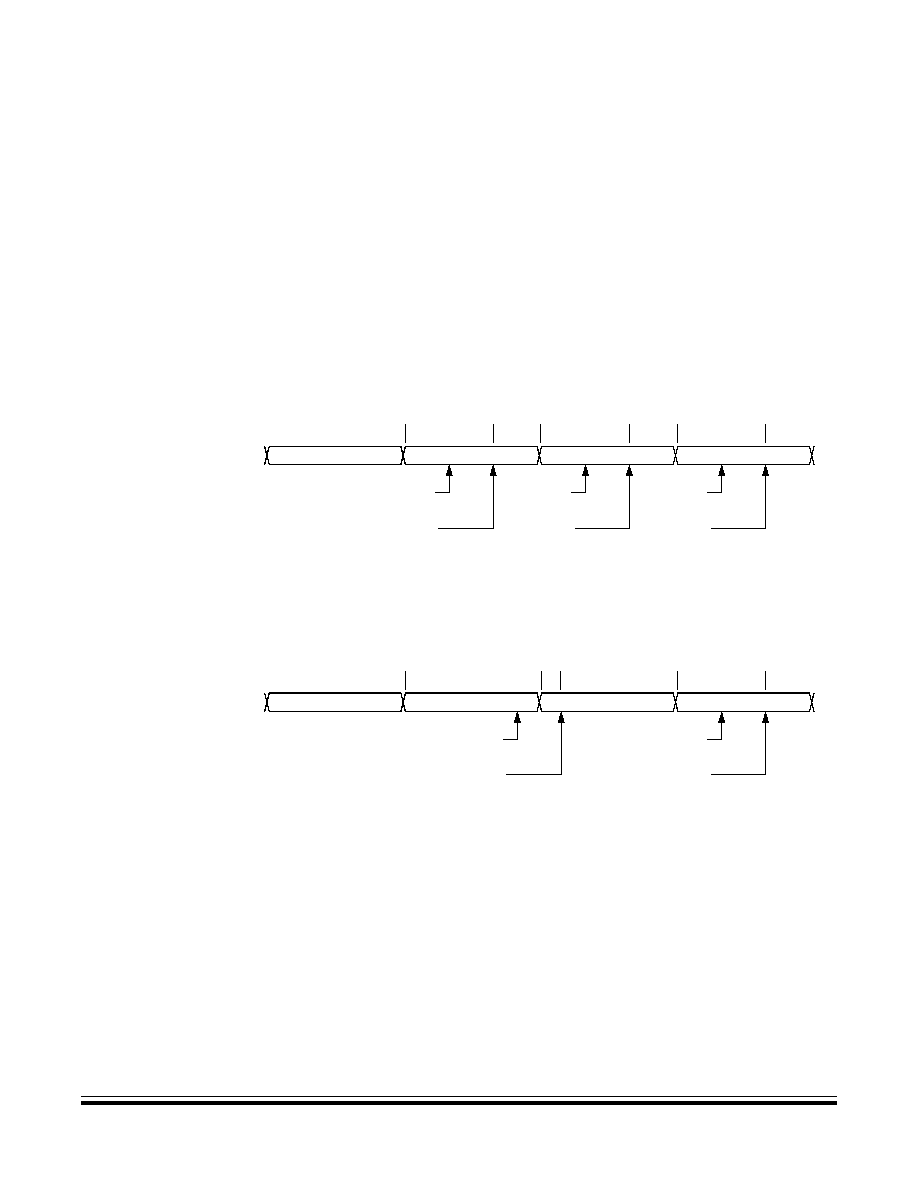
Enhanced Serial Communications Interface (ESCI) Module
I/O Registers
MC68HC908GR16 -- Rev. 1.0
Data Sheet
MOTOROLA
Enhanced Serial Communications Interface (ESCI) Module
183
In applications that are subject to software latency or in which it is important to
know which byte is lost due to an overrun, the flag-clearing routine can check
the OR bit in a second read of SCS1 after reading the data register.
NF -- Receiver Noise Flag Bit
This clearable, read-only bit is set when the ESCI detects noise on the RxD pin.
NF generates an NF CPU interrupt request if the NEIE bit in SCC3 is also set.
Clear the NF bit by reading SCS1 and then reading the SCDR. Reset clears the
NF bit.
1 = Noise detected
0 = No noise detected
Figure 14-14. Flag Clearing Sequence
FE -- Receiver Framing Error Bit
This clearable, read-only bit is set when a logic 0 is accepted as the stop bit. FE
generates an ESCI error CPU interrupt request if the FEIE bit in SCC3 also is
set. Clear the FE bit by reading SCS1 with FE set and then reading the SCDR.
Reset clears the FE bit.
1 = Framing error detected
0 = No framing error detected
PE -- Receiver Parity Error Bit
This clearable, read-only bit is set when the ESCI detects a parity error in
incoming data. PE generates a PE CPU interrupt request if the PEIE bit in SCC3
BYTE 1
NORMAL FLAG CLEARING SEQUENCE
READ SCS1
SCRF = 1
READ SCDR
BYTE 1
SC
R
F
=
1
SC
R
F
=
1
BYTE 2
BYTE 3
BYTE 4
OR = 0
READ SCS1
SCRF = 1
OR = 0
READ SCDR
BYTE 2
SC
R
F
=
0
READ SCS1
SCRF = 1
OR = 0
SCRF
=
1
SCRF
=
0
READ SCDR
BYTE 3
SC
R
F
=
0
BYTE 1
READ SCS1
SCRF = 1
READ SCDR
BYTE 1
SCRF
=
1
SCRF
=
1
BYTE 2
BYTE 3
BYTE 4
OR = 0
READ SCS1
SCRF = 1
OR = 1
READ SCDR
BYTE 3
DELAYED FLAG CLEARING SEQUENCE
OR = 1
SCRF
=
1
OR = 1
SCRF
=
0
OR = 1
SCRF
=
0
OR = 0
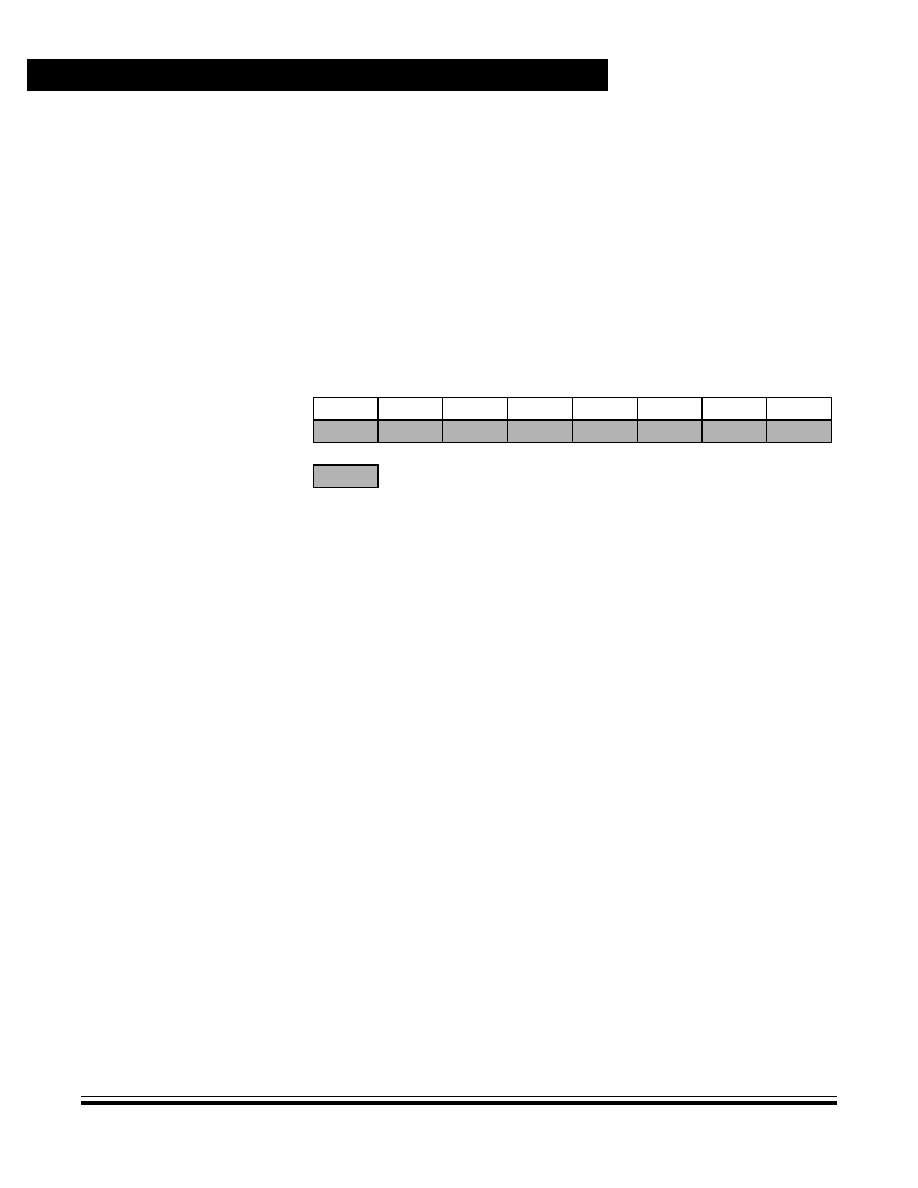
Enhanced Serial Communications Interface (ESCI) Module
Data Sheet
MC68HC908GR16 -- Rev. 1.0
184
Enhanced Serial Communications Interface (ESCI) Module
MOTOROLA
is also set. Clear the PE bit by reading SCS1 with PE set and then reading the
SCDR. Reset clears the PE bit.
1 = Parity error detected
0 = No parity error detected
14.8.5 ESCI Status Register 2
ESCI status register 2 (SCS2) contains flags to signal these conditions:
�
Break character detected
�
Incoming data
BKF -- Break Flag Bit
This clearable, read-only bit is set when the ESCI detects a break character on
the RxD pin. In SCS1, the FE and SCRF bits are also set. In 9-bit character
transmissions, the R8 bit in SCC3 is cleared. BKF does not generate a CPU
interrupt request. Clear BKF by reading SCS2 with BKF set and then reading
the SCDR. Once cleared, BKF can become set again only after logic 1s again
appear on the RxD pin followed by another break character. Reset clears the
BKF bit.
1 = Break character detected
0 = No break character detected
RPF -- Reception in Progress Flag Bit
This read-only bit is set when the receiver detects a logic 0 during the RT1 time
period of the start bit search. RPF does not generate an interrupt request. RPF
is reset after the receiver detects false start bits (usually from noise or a baud
rate mismatch), or when the receiver detects an idle character. Polling RPF
before disabling the ESCI module or entering stop mode can show whether a
reception is in progress.
1 = Reception in progress
0 = No reception in progress
Address:
$0017
Bit 7
6
5
4
3
2
1
Bit 0
Read:
0
0
0
0
0
0
BKF
RPF
Write:
Reset:
0
0
0
0
0
0
0
0
= Unimplemented
Figure 14-15. ESCI Status Register 2 (SCS2)
Enhanced Serial Communications Interface (ESCI) Module
I/O Registers
MC68HC908GR16 -- Rev. 1.0
Data Sheet
MOTOROLA
Enhanced Serial Communications Interface (ESCI) Module
185
14.8.6 ESCI Data Register
The ESCI data register (SCDR) is the buffer between the internal data bus and the
receive and transmit shift registers. Reset has no effect on data in the ESCI data
register.
R7/T7:R0/T0 -- Receive/Transmit Data Bits
Reading address $0018 accesses the read-only received data bits, R7:R0.
Writing to address $0018 writes the data to be transmitted, T7:T0. Reset has no
effect on the ESCI data register.
NOTE:
Do not use read-modify-write instructions on the ESCI data register.
14.8.7 ESCI Baud Rate Register
The ESCI baud rate register (SCBR) together with the ESCI prescaler register
selects the baud rate for both the receiver and the transmitter.
NOTE:
There are two prescalers available to adjust the baud rate. One in the ESCI baud
rate register and one in the ESCI prescaler register.
LINT -- LIN Break Symbol Transmit Enable
This read/write bit selects the enhanced ESCI features for master nodes in the
local interconnect network (LIN) protocol (version 1.2) as shown in
Table 14-6
.
Reset clears LINT.
Address:
$0018
Bit 7
6
5
4
3
2
1
Bit 0
Read:
R7
R6
R5
R4
R3
R2
R1
R0
Write:
T7
T6
T5
T4
T3
T2
T1
T0
Reset:
Unaffected by reset
Figure 14-16. ESCI Data Register (SCDR)
Address:
$0019
Bit 7
6
5
4
3
2
1
Bit 0
Read:
LINT
LINR
SCP1
SCP0
R
SCR2
SCR1
SCR0
Write:
Reset:
0
0
0
0
0
0
0
0
= Unimplemented
R
= Reserved
Figure 14-17. ESCI Baud Rate Register (SCBR)
Enhanced Serial Communications Interface (ESCI) Module
Data Sheet
MC68HC908GR16 -- Rev. 1.0
186
Enhanced Serial Communications Interface (ESCI) Module
MOTOROLA
NOTE:
LIN master nodes require significantly tighter timing tolerances than slave nodes.
Be sure to consult the current LIN specification to ensure that timing requirements
are met properly. Generally, these timing tolerances require crystals or oscillators
to be used, rather than internal clocking circuits.
LINR -- LIN Break Symbol Receiver Bits
This read/write bit selects the enhanced ESCI features for slave nodes in the
local interconnect network (LIN) protocol as shown in
Table 14-7
. Reset clears
LINR.
In LIN (version 1.2) systems, the master node transmits a break character which
will appear as 11.05�14.95 dominant bits to the slave node. A data character of
0x00 sent from the master might appear as 7.65�10.35 dominant bit times. This
is due to the oscillator tolerance requirement that the slave node must be within
�15% of the master node's oscillator. Since a slave node cannot know if it is
running faster or slower than the master node (prior to synchronization), the
LINR bit allows the slave node to differentiate between a 0x00 character of
10.35 bits and a break character of 11.05 bits. The break symbol length must be
verified in software in any case, but the LINR bit serves as a filter, preventing
false detections of break characters that are really 0x00 data characters.
SCP1 and SCP0 -- ESCI Baud Rate Register Prescaler Bits
These read/write bits select the baud rate register prescaler divisor as shown in
Table 14-8
. Reset clears SCP1 and SCP0.
Table 14-6. ESCI LIN Master Node Control Bits
LINT
M
Functionality
0
X
Normal ESCI functionality
1
0
13-bit generation enabled for LIN transmitter
1
1
14-bit generation enabled for LIN transmitter
Table 14-7. ESCI LIN Slave Node Control Bits
LINR
M
Functionality
0
X
Normal ESCI functionality
1
0
11-bit break detect enabled for LIN receiver
1
1
12-bit break detect enabled for LIN receiver
Table 14-8. ESCI Baud Rate Prescaling
SCP[1:0]
Baud Rate Register
Prescaler Divisor (BPD)
0 0
1
0 1
3
1 0
4
1 1
13
Enhanced Serial Communications Interface (ESCI) Module
I/O Registers
MC68HC908GR16 -- Rev. 1.0
Data Sheet
MOTOROLA
Enhanced Serial Communications Interface (ESCI) Module
187
SCR2�SCR0 -- ESCI Baud Rate Select Bits
These read/write bits select the ESCI baud rate divisor as shown in
Table 14-9
.
Reset clears SCR2�SCR0.
14.8.8 ESCI Prescaler Register
The ESCI prescaler register (SCPSC) together with the ESCI baud rate register
selects the baud rate for both the receiver and the transmitter.
NOTE:
There are two prescalers available to adjust the baud rate. One in the ESCI baud
rate register and one in the ESCI prescaler register.
PDS2�PDS0 -- Prescaler Divisor Select Bits
These read/write bits select the prescaler divisor as shown in
Table 14-10
. Reset clears PDS2�PDS0.
NOTE:
The setting of `000' will bypass this prescaler. It is not recommended to bypass the
prescaler while ENSCI is set, because the switching is not glitch free.
Table 14-9. ESCI Baud Rate Selection
SCR[2:1:0]
Baud Rate Divisor (BD)
0 0 0
1
0 0 1
2
0 1 0
4
0 1 1
8
1 0 0
16
1 0 1
32
1 1 0
64
1 1 1
128
Address:
$0009
Bit 7
6
5
4
3
2
1
Bit 0
Read:
PDS2
PDS1
PDS0
PSSB4
PSSB3
PSSB2
PSSB1
PSSB0
Write:
Reset:
0
0
0
0
0
0
0
0
Figure 14-18. ESCI Prescaler Register (SCPSC)
Enhanced Serial Communications Interface (ESCI) Module
Data Sheet
MC68HC908GR16 -- Rev. 1.0
188
Enhanced Serial Communications Interface (ESCI) Module
MOTOROLA
PSSB4�PSSB0 -- Clock Insertion Select Bits
These read/write bits select the number of clocks inserted in each 32 output
cycle frame to achieve more timing resolution on the average prescaler
frequency as shown in
Table 14-11
. Reset clears PSSB4�PSSB0.
Use the following formula to calculate the ESCI baud rate:
where:
SCI clock source = f
Bus
or CGMXCLK (selected by SCIBDSRC in the
CONFIG2 register)
BPD = Baud rate register prescaler divisor
BD = Baud rate divisor
PD = Prescaler divisor
PDFA = Prescaler divisor fine adjust
Table 14-12
shows the ESCI baud rates that can be generated with a 4.9152-MHz
bus frequency.
Table 14-10. ESCI Prescaler Division Ratio
PS[2:1:0]
Prescaler Divisor (PD)
0 0 0
Bypass this prescaler
0 0 1
2
0 1 0
3
0 1 1
4
1 0 0
5
1 0 1
6
1 1 0
7
1 1 1
8
Baud rate
SCI clock source
64
BPD
BD
PD
PDFA
+
(
)
�
�
�
------------------------------------------------------------------------------------
=

Enhanced Serial Communications Interface (ESCI) Module
I/O Registers
MC68HC908GR16 -- Rev. 1.0
Data Sheet
MOTOROLA
Enhanced Serial Communications Interface (ESCI) Module
189
Table 14-11. ESCI Prescaler Divisor Fine Adjust
PSSB[4:3:2:1:0]
Prescaler Divisor Fine Adjust (PDFA)
0 0 0 0 0
0/32 = 0
0 0 0 0 1
1/32 = 0.03125
0 0 0 1 0
2/32 = 0.0625
0 0 0 1 1
3/32 = 0.09375
0 0 1 0 0
4/32 = 0.125
0 0 1 0 1
5/32 = 0.15625
0 0 1 1 0
6/32 = 0.1875
0 0 1 1 1
7/32 = 0.21875
0 1 0 0 0
8/32 = 0.25
0 1 0 0 1
9/32 = 0.28125
0 1 0 1 0
10/32 = 0.3125
0 1 0 1 1
11/32 = 0.34375
0 1 1 0 0
12/32 = 0.375
0 1 1 0 1
13/32 = 0.40625
0 1 1 1 0
14/32 = 0.4375
0 1 1 1 1
15/32 = 0.46875
1 0 0 0 0
16/32 = 0.5
1 0 0 0 1
17/32 = 0.53125
1 0 0 1 0
18/32 = 0.5625
1 0 0 1 1
19/32 = 0.59375
1 0 1 0 0
20/32 = 0.625
1 0 1 0 1
21/32 = 0.65625
1 0 1 1 0
22/32 = 0.6875
1 0 1 1 1
23/32 = 0.71875
1 1 0 0 0
24/32 = 0.75
1 1 0 0 1
25/32 = 0.78125
1 1 0 1 0
26/32 = 0.8125
1 1 0 1 1
27/32 = 0.84375
1 1 1 0 0
28/32 = 0.875
1 1 1 0 1
29/32 = 0.90625
1 1 1 1 0
30/32 = 0.9375
1 1 1 1 1
31/32 = 0.96875
Enhanced Serial Communications Interface (ESCI) Module
Data Sheet
MC68HC908GR16 -- Rev. 1.0
190
Enhanced Serial Communications Interface (ESCI) Module
MOTOROLA
Table 14-12. ESCI Baud Rate Selection Examples
PS[2:1:0]
PSSB[4:3:2:1:0]
SCP[1:0]
Prescaler
Divisor
(BPD)
SCR[2:1:0]
Baud Rate
Divisor
(BD)
Baud Rate
(f
Bus
= 4.9152 MHz)
0 0 0
X X X X X
0 0
1
0 0 0
1
76,800
1 1 1
0 0 0 0 0
0 0
1
0 0 0
1
9600
1 1 1
0 0 0 0 1
0 0
1
0 0 0
1
9562.65
1 1 1
0 0 0 1 0
0 0
1
0 0 0
1
9525.58
1 1 1
1 1 1 1 1
0 0
1
0 0 0
1
8563.07
0 0 0
X X X X X
0 0
1
0 0 1
2
38,400
0 0 0
X X X X X
0 0
1
0 1 0
4
19,200
0 0 0
X X X X X
0 0
1
0 1 1
8
9600
0 0 0
X X X X X
0 0
1
1 0 0
16
4800
0 0 0
X X X X X
0 0
1
1 0 1
32
2400
0 0 0
X X X X X
0 0
1
1 1 0
64
1200
0 0 0
X X X X X
0 0
1
1 1 1
128
600
0 0 0
X X X X X
0 1
3
0 0 0
1
25,600
0 0 0
X X X X X
0 1
3
0 0 1
2
12,800
0 0 0
X X X X X
0 1
3
0 1 0
4
6400
0 0 0
X X X X X
0 1
3
0 1 1
8
3200
0 0 0
X X X X X
0 1
3
1 0 0
16
1600
0 0 0
X X X X X
0 1
3
1 0 1
32
800
0 0 0
X X X X X
0 1
3
1 1 0
64
400
0 0 0
X X X X X
0 1
3
1 1 1
128
200
0 0 0
X X X X X
1 0
4
0 0 0
1
19,200
0 0 0
X X X X X
1 0
4
0 0 1
2
9600
0 0 0
X X X X X
1 0
4
0 1 0
4
4800
0 0 0
X X X X X
1 0
4
0 1 1
8
2400
0 0 0
X X X X X
1 0
4
1 0 0
16
1200
0 0 0
X X X X X
1 0
4
1 0 1
32
600
0 0 0
X X X X X
1 0
4
1 1 0
64
300
0 0 0
X X X X X
1 0
4
1 1 1
128
150
0 0 0
X X X X X
1 1
13
0 0 0
1
5908
0 0 0
X X X X X
1 1
13
0 0 1
2
2954
0 0 0
X X X X X
1 1
13
0 1 0
4
1477
0 0 0
X X X X X
1 1
13
0 1 1
8
739
0 0 0
X X X X X
1 1
13
1 0 0
16
369
0 0 0
X X X X X
1 1
13
1 0 1
32
185
0 0 0
X X X X X
1 1
13
1 1 0
64
92
0 0 0
X X X X X
1 1
13
1 1 1
128
46
Enhanced Serial Communications Interface (ESCI) Module
ESCI Arbiter
MC68HC908GR16 -- Rev. 1.0
Data Sheet
MOTOROLA
Enhanced Serial Communications Interface (ESCI) Module
191
14.9 ESCI Arbiter
The ESCI module comprises an arbiter module designed to support software for
communication tasks as bus arbitration, baud rate recovery and break time
detection. The arbiter module consists of an 9-bit counter with 1-bit overflow and
control logic. The CPU can control operation mode via the ESCI arbiter control
register (SCIACTL).
14.9.1 ESCI Arbiter Control Register
AM1 and AM0 -- Arbiter Mode Select Bits
These read/write bits select the mode of the arbiter module as shown in
Table
14-13
. Reset clears AM1 and AM0.
ALOST -- Arbitration Lost Flag
This read-only bit indicates loss of arbitration. Clear ALOST by writing a logic 0
to AM1. Reset clears ALOST.
ACLK -- Arbiter Counter Clock Select Bit
This read/write bit selects the arbiter counter clock source. Reset clears ACLK.
1 = Arbiter counter is clocked with one half of the ESCI input clock generated
by the ESCI prescaler
0 = Arbiter counter is clocked with one half of the bus clock
AFIN-- Arbiter Bit Time Measurement Finish Flag
This read-only bit indicates bit time measurement has finished. Clear AFIN by
writing any value to SCIACTL. Reset clears AFIN.
1 = Bit time measurement has finished
0 = Bit time measurement not yet finished
Address:
$000A
Bit 7
6
5
4
3
2
1
Bit 0
Read:
AM1
ALOST
AM0
ACLK
AFIN
ARUN
AROVFL
ARD8
Write:
Reset:
0
0
0
0
0
0
0
0
= Unimplemented
Figure 14-19. ESCI Arbiter Control Register (SCIACTL)
Table 14-13. ESCI Arbiter Selectable Modes
AM[1:0]
ESCI Arbiter Mode
0 0
Idle / counter reset
0 1
Bit time measurement
1 0
Bus arbitration
1 1
Reserved / do not use
Enhanced Serial Communications Interface (ESCI) Module
Data Sheet
MC68HC908GR16 -- Rev. 1.0
192
Enhanced Serial Communications Interface (ESCI) Module
MOTOROLA
ARUN-- Arbiter Counter Running Flag
This read-only bit indicates the arbiter counter is running. Reset clears ARUN.
1 = Arbiter counter running
0 = Arbiter counter stopped
AROVFL-- Arbiter Counter Overflow Bit
This read-only bit indicates an arbiter counter overflow. Clear AROVFL by
writing any value to SCIACTL. Writing logic 0s to AM1 and AM0 resets the
counter keeps it in this idle state. Reset clears AROVFL.
1 = Arbiter counter overflow has occurred
0 = No arbiter counter overflow has occurred
ARD8-- Arbiter Counter MSB
This read-only bit is the MSB of the 9-bit arbiter counter. Clear ARD8 by writing
any value to SCIACTL. Reset clears ARD8.
14.9.2 ESCI Arbiter Data Register
ARD7�ARD0 -- Arbiter Least Significant Counter Bits
These read-only bits are the eight LSBs of the 9-bit arbiter counter. Clear
ARD7�ARD0 by writing any value to SCIACTL. Writing logic 0s to AM1 and AM0
permanently resets the counter and keeps it in this idle state. Reset clears
ARD7�ARD0.
14.9.3 Bit Time Measurement
Two bit time measurement modes, described here, are available according to the
state of ACLK.
1.
ACLK = 0 -- The counter is clocked with one half of the bus clock. The
counter is started when a falling edge on the RxD pin is detected. The
counter will be stopped on the next falling edge. ARUN is set while the
counter is running, AFIN is set on the second falling edge on RxD (for
instance, the counter is stopped). This mode is used to recover the received
baud rate. See
Figure 14-21
.
2.
ACLK = 1 -- The counter is clocked with one half of the ESCI input clock
generated by the ESCI prescaler. The counter is started when a logic 0 is
detected on RxD (see
Figure 14-22
). A logic 0 on RxD on enabling the bit
time measurement with ACLK = 1 leads to immediate start of the counter
(see
Figure 14-23
). The counter will be stopped on the next rising edge of
RxD. This mode is used to measure the length of a received break.
Address: $000B
Bit 7
6
5
4
3
2
1
Bit 0
Read:
ARD7
ARD6
ARD5
ARD4
ARD3
ARD2
ARD1
ARD0
Write:
Reset:
0
0
0
0
0
0
0
0
= Unimplemented
Figure 14-20. ESCI Arbiter Data Register (SCIADAT)
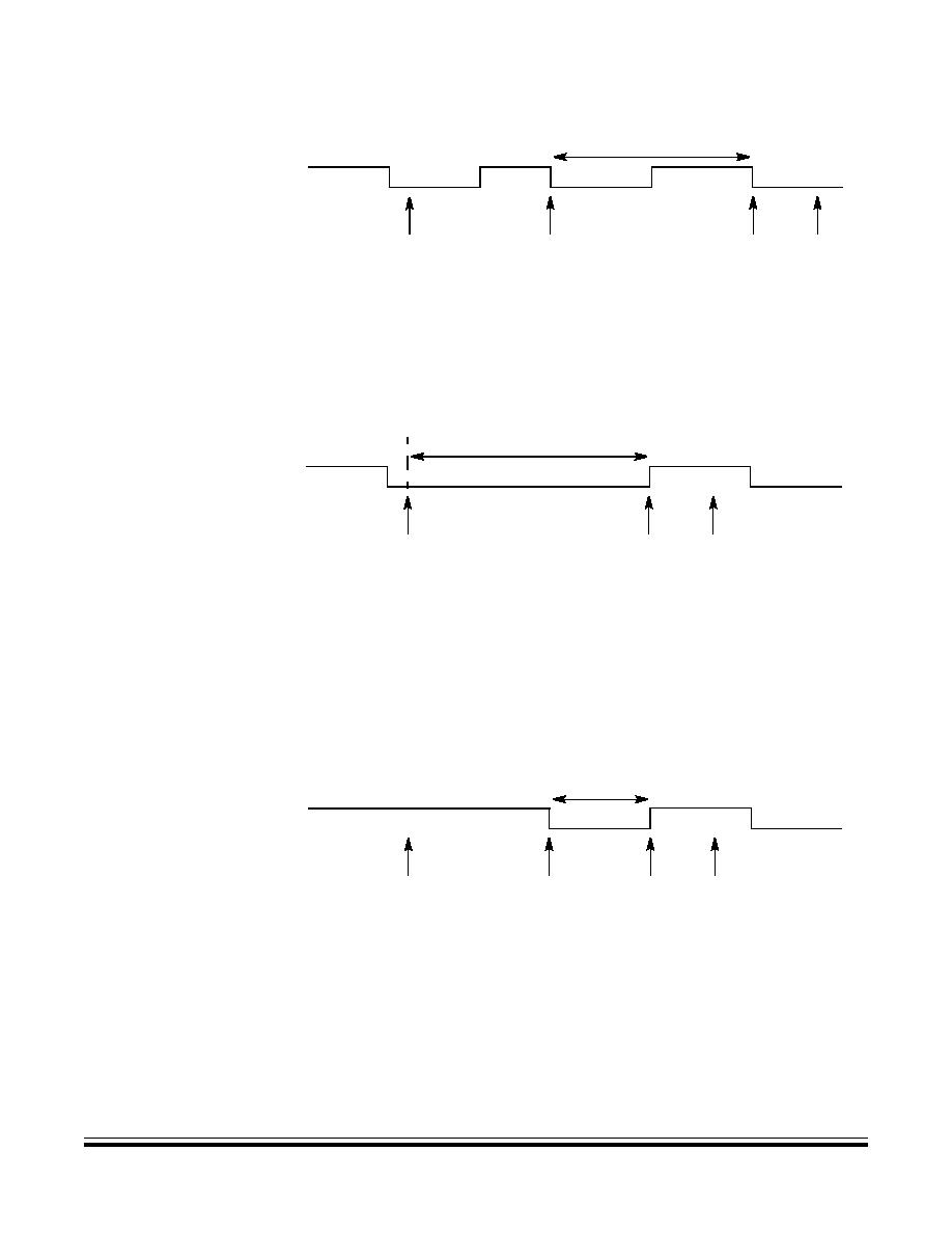
Enhanced Serial Communications Interface (ESCI) Module
ESCI Arbiter
MC68HC908GR16 -- Rev. 1.0
Data Sheet
MOTOROLA
Enhanced Serial Communications Interface (ESCI) Module
193
Figure 14-21. Bit Time Measurement with ACLK = 0
Figure 14-22. Bit Time Measurement with ACLK = 1, Scenario A
Figure 14-23. Bit Time Measurement with ACLK = 1, Scenario B
CPU WR
ITES
SCIA
C
T
L
COU
N
TER STAR
TS
,
COUNTER STOPS
,
MEASURED TIME
CPU READS RESULT
RXD
W
I
TH
$2
0
AR
UN = 1
AF
IN = 1
OUT OF SCIAD
A
T
CP
U WR
IT
ES SC
IA
C
TL
WITH
$3
0
COU
N
TER STAR
TS
, AR
UN
= 1
COUNT
ER STOPS
,
AFIN
=
1
MEASURED TIME
C
PU RE
ADS R
ESULT
OUT
RXD
OF
SCIAD
A
T
CPU
WR
ITES
SCIA
C
T
L
C
O
UNTER STAR
TS
,
COUNTER STOPS
,
MEASURED TIME
CPU READS RESULT
RXD
OUT OF SCIAD
A
T
AF
I
N
=
1
AR
UN
=
1
W
I
TH
$3
0

Enhanced Serial Communications Interface (ESCI) Module
Data Sheet
MC68HC908GR16 -- Rev. 1.0
194
Enhanced Serial Communications Interface (ESCI) Module
MOTOROLA
14.9.4 Arbitration Mode
If AM[1:0] is set to 10, the arbiter module operates in arbitration mode. On every
rising edge of SCI_TxD (output of the ESCI module, internal chip signal), the
counter is started. When the counter reaches $38 (ACLK = 0) or $08 (ACLK = 1),
RxD is statically sensed. If in this case, RxD is sensed low (for example, another
bus is driving the bus dominant) ALOST is set. As long as ALOST is set, the TxD
pin is forced to 1, resulting in a seized transmission.
If SCI_TxD is sensed logic 0 without having sensed a logic 0 before on RxD, the
counter will be reset, arbitration operation will be restarted after the next rising edge
of SCI_TxD.

MC68HC908GR16 -- Rev. 1.0
Data Sheet
MOTOROLA
System Integration Module (SIM)
195
Data Sheet -- MC68HC908GR16
Section 15. System Integration Module (SIM)
15.1 Introduction
This section describes the system integration module (SIM). Together with the
central processor unit (CPU), the SIM controls all microcontroller unit (MCU)
activities. A block diagram of the SIM is shown in
Figure 15-2
.
Table 15-1
is a
summary of the SIM input/output (I/O) registers. The SIM is a system state
controller that coordinates CPU and exception timing.
The SIM is responsible for:
�
Bus clock generation and control for CPU and peripherals:
�
Stop/wait/reset/break entry and recovery
�
Internal clock control
�
Master reset control, including power-on reset (POR) and computer
operating properly (COP) timeout
�
Interrupt control:
�
Acknowledge timing
�
Arbitration control timing
�
Vector address generation
�
CPU enable/disable timing
�
Modular architecture expandable to 128 interrupt sources
Table 15-1
shows the internal signal names used in this section.
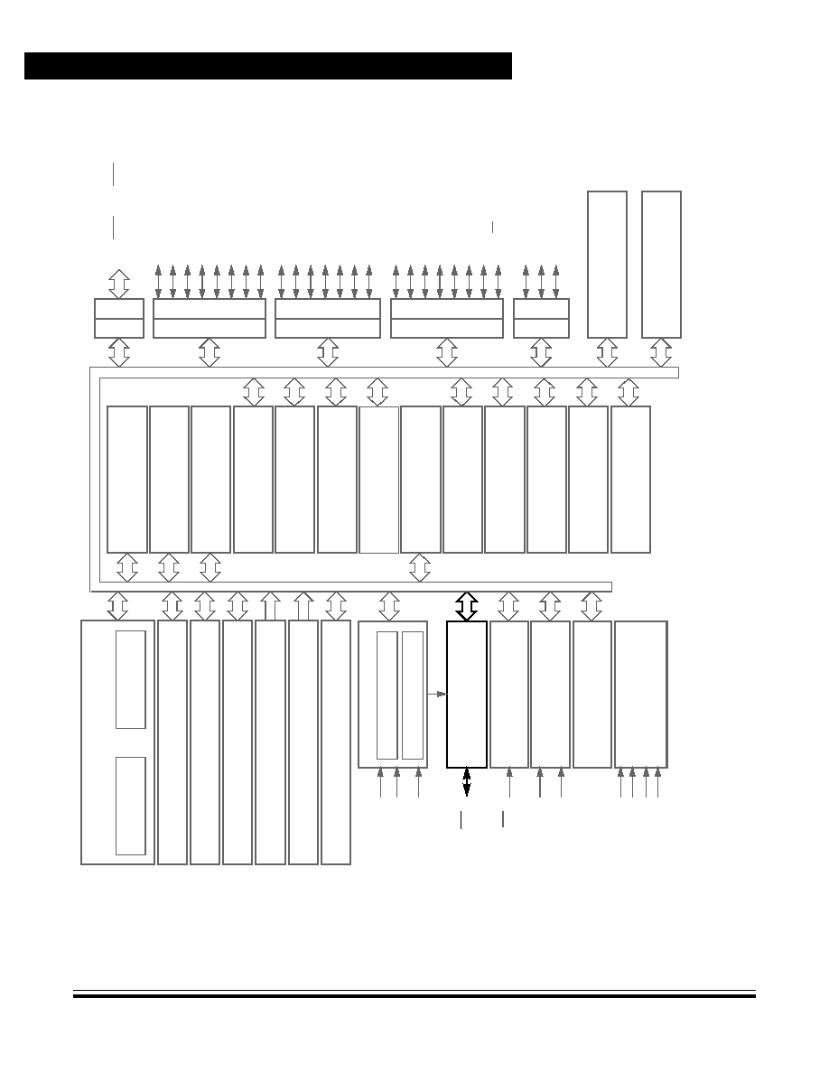
Data Sheet
MC6
8
HC90
8
GR16 --
Re
v. 1.0
196
System Integra
t
i
on
Modul
e (SIM)
M
OTOROLA
System Integration Module (SIM)
Figure 15-1. Block Diagram Highlight SIM Block and Pins
MONITOR MODULE
M68HC08 CPU
CONTROL AND STATUS REGISTERS -- 64 BYTES
USER FLASH -- 15,872 BYTES
USER RAM -- 1024 BYTES
MONITOR ROM -- 350 BYTES
USER FLASH VECTOR SPACE -- 44 BYTES
PORTA
D
DRA
DDRC
PO
R
T
C
DDR
D
PORTD
DDRE
POR
T
E
INTERNAL BUS
OSC1
OSC2
RST
(3)
IRQ
(3)
PTA7/KBD7�PTA0/KBD0
(1)
PTB7/AD7
PTB6/AD6
PTB5/AD5
PTB4/AD4
PTB3/AD3
PTB2/AD2
PTB1/AD1
PTB0/AD0
PTC6
(1)
PTC5
(1)
PTC4
(1), (2)
PTC3
(1), (2)
PTC2
(1), (2)
PTC1
(1), (2)
PTC0
(1), (2)
PTD7/T2CH1
(1)
PTD6/T2CH0
(1)
PTD5/T1CH1
(1)
PTD4/T1CH0
(1)
PTD3/SPSCK
(1)
PTD2/MOSI
(1)
PTD1/MISO
(1)
PTD0/SS
(1)
PTE1/RxD
PTE0/TxD
SECURITY
MODULE
POWER
V
SS
V
DD
V
SSA
V
DDA
1. Ports are software configurable with pullup device if input port.
2. Higher current drive port pins
3. Pin contains integrated pullup device
MONITOR MODE ENTRY
MODULE
DDRB
PORTB
V
DDAD
/V
REFH
V
DDAD
/V
REFL
PTE5�PTE2
FLASH PROGRAMMING ROUTINES ROM -- 406 BYTES
CLOCK GENERATOR MODULE
CGMXFC
PHASE LOCKED LOOP
32�100 kHz OSCILLATOR
CPU
REGISTERS
ARITHMETIC/LOGIC
UNIT (ALU)
SYSTEM INTEGRATION
MODULE
SINGLE EXTERNAL
INTERRUPT MODULE
10-BIT ANALOG-TO-DIGITAL
CONVERTER MODULE
POWER-ON RESET
MODULE
PROGRAMMABLE TIMEBASE
MODULE
SINGLE BREAKPOINT
BREAK MODULE
DUAL VOLTAGE
LOW-VOLTAGE INHIBIT
MODULE
8-BIT KEYBOARD
INTERRUPT MODULE
2-CHANNEL TIMER
INTERFACE MODULE 1
2-CHANNEL TIMER
INTERFACE MODULE 2
ENHANCED SERIAL
COMUNICATIONS
INTERFACE MODULE
COMPUTER OPERATING
PROPERLY MODULE
SERIAL PERIPHERAL
INTERFACE MODULE
DATA BUS SWITCH
MODULE
MEMORY MAP
MODULE
CONFIGURATION
REGISTER 1�2
MODULE
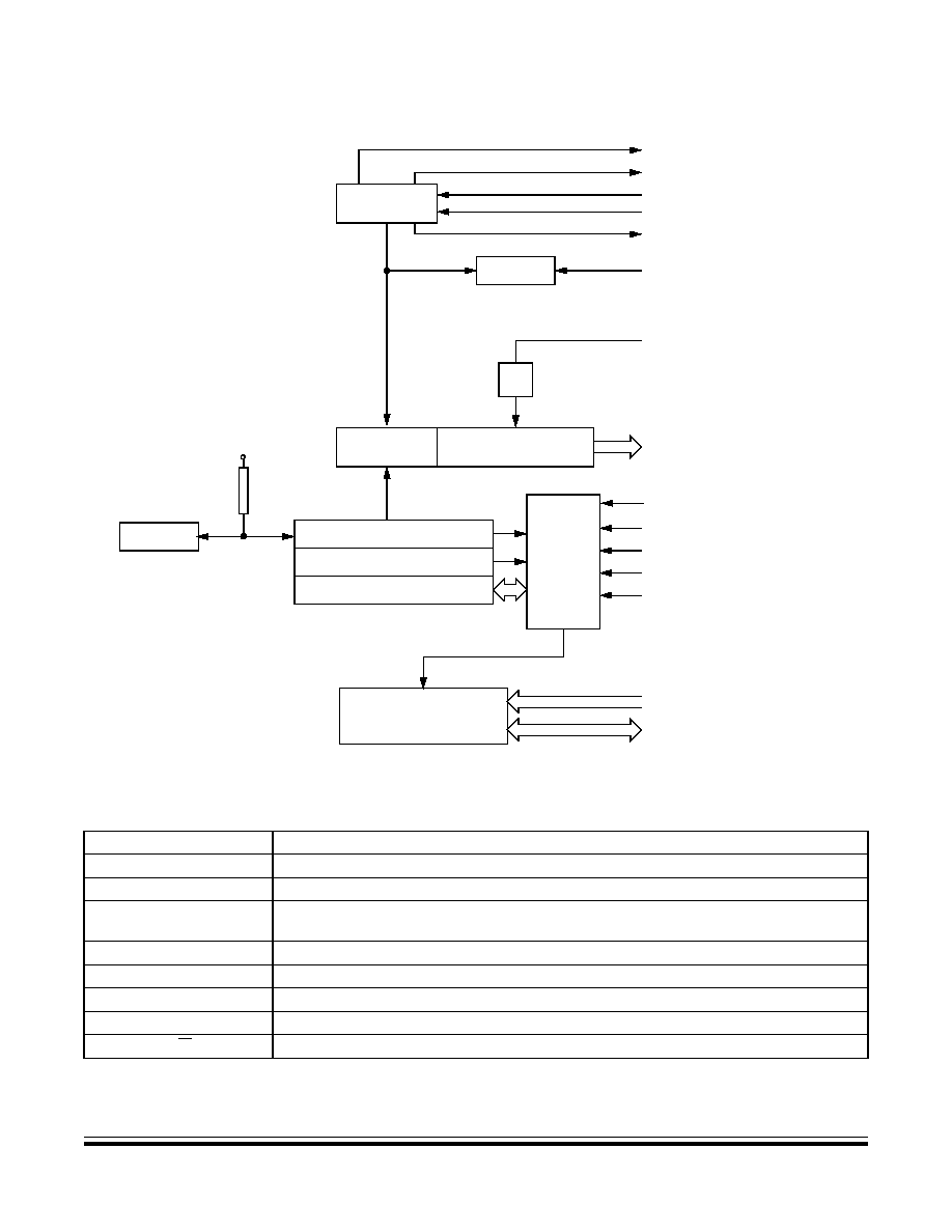
System Integration Module (SIM)
Introduction
MC68HC908GR16 -- Rev. 1.0
Data Sheet
MOTOROLA
System Integration Module (SIM)
197
Figure 15-2. SIM Block Diagram
STOP/WAIT
CLOCK
CONTROL
CLOCK GENERATORS
POR CONTROL
RESET PIN CONTROL
SIM RESET STATUS REGISTER
INTERRUPT CONTROL
AND PRIORITY DECODE
MODULE STOP
MODULE WAIT
CPU STOP (FROM CPU)
CPU WAIT (FROM CPU)
SIMOSCEN (TO CGM)
CGMOUT (FROM CGM)
INTERNAL CLOCKS
MASTER
RESET
CONTROL
RESET
PIN LOGIC
LVI (FROM LVI MODULE)
ILLEGAL OPCODE (FROM CPU)
ILLEGAL ADDRESS (FROM ADDRESS
MAP DECODERS)
COP (FROM COP MODULE)
INTERRUPT SOURCES
CPU INTERFACE
RESET
CONTROL
SIM
COUNTER
CGMXCLK (FROM CGM)
� 2
V
DD
INTERNAL
PULLUP
DEVICE
FORCED MONITOR MODE ENTRY
Table 15-1. Signal Name Conventions
Signal Name
Description
CGMXCLK
Buffered version of OSC1 from clock generator module (CGM)
CGMVCLK
PLL output
CGMOUT
PLL-based or OSC1-based clock output from CGM module
(Bus clock = CGMOUT divided by two)
IAB
Internal address bus
IDB
Internal data bus
PORRST
Signal from the power-on reset module to the SIM
IRST
Internal reset signal
R/W
Read/write signal
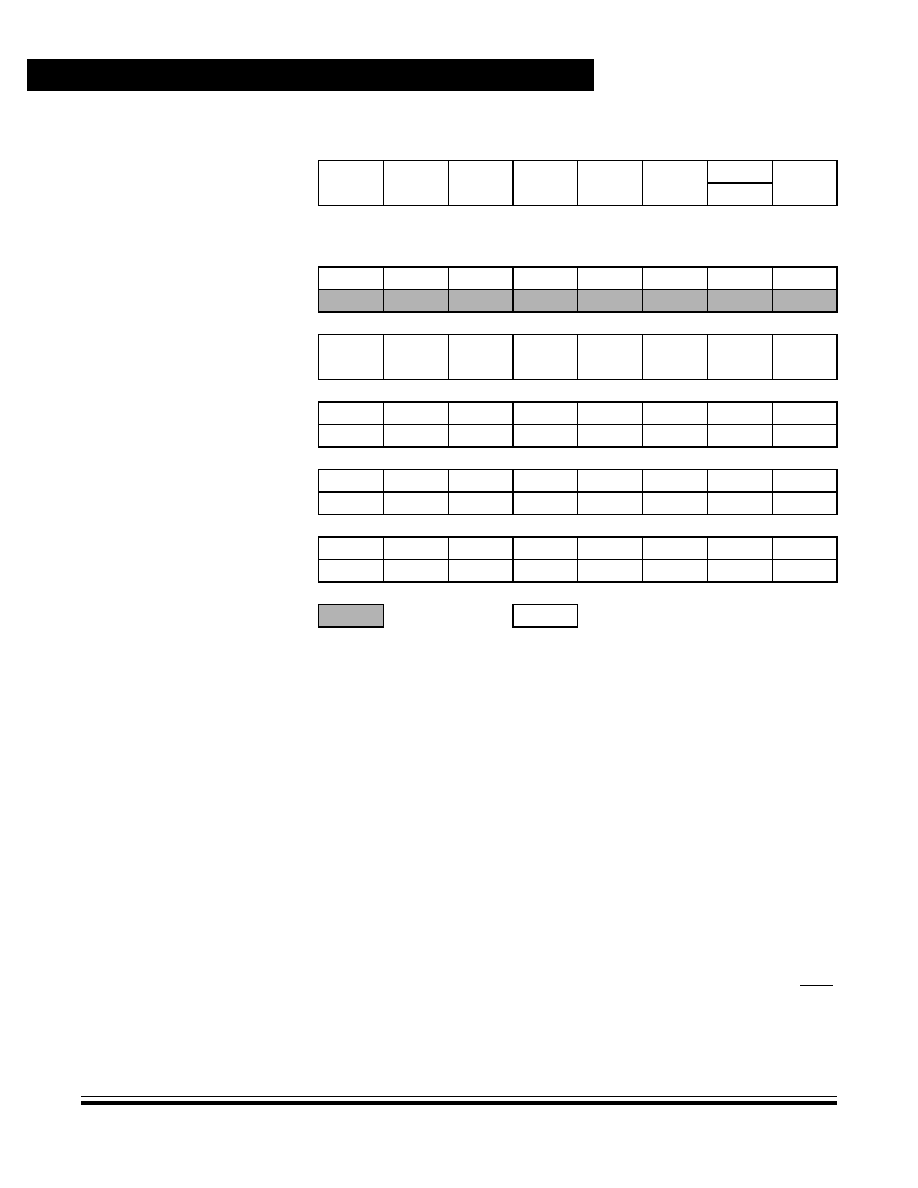
System Integration Module (SIM)
Data Sheet
MC68HC908GR16 -- Rev. 1.0
198
System Integration Module (SIM)
MOTOROLA
15.2 SIM Bus Clock Control and Generation
The bus clock generator provides system clock signals for the CPU and peripherals
on the MCU. The system clocks are generated from an incoming clock, CGMOUT,
as shown in
Figure 15-4
. This clock originates from either an external oscillator or
from the on-chip PLL.
15.2.1 Bus Timing
In user mode, the internal bus frequency is either the crystal oscillator output
(CGMXCLK) divided by four or the PLL output (CGMVCLK) divided by four.
15.2.2 Clock Startup from POR or LVI Reset
When the power-on reset module or the low-voltage inhibit module generates a
reset, the clocks to the CPU and peripherals are inactive and held in an inactive
phase until after the 4096 CGMXCLK cycle POR timeout has completed. The RST
pin is driven low by the SIM during this entire period. The IBUS clocks start upon
completion of the timeout.
Addr.
Register Name
Bit 7
6
5
4
3
2
1
Bit 0
$FE00
Break Status Register
(BSR)
See page 212.
Read:
R
R
R
R
R
R
SBSW
R
Write:
Note
(1)
Reset:
0
0
0
0
0
0
0
0
1. Writing a logic 0 clears SBSW.
$FE01
SIM Reset Status Register
(SRSR)
See page 213.
Read:
POR
PIN
COP
ILOP
ILAD
MODRST
LVI
0
Write:
POR:
1
0
0
0
0
0
0
0
$FE03
Break Flag Control Register
(BFCR)
See page 214.
Read:
BCFE
R
R
R
R
R
R
R
Write:
Reset:
0
$FE04
Interrupt Status Register 1
(INT1)
See page 208.
Read:
IF6
IF5
IF4
IF3
IF2
IF1
0
0
Write:
R
R
R
R
R
R
R
R
Reset:
0
0
0
0
0
0
0
0
$FE05
Interrupt Status Register 2
(INT2)
See page 208.
Read:
IF14
IF13
IF12
IF11
IF10
IF9
IF8
IF7
Write:
R
R
R
R
R
R
R
R
Reset:
0
0
0
0
0
0
0
0
$FE06
Interrupt Status Register 3
(INT3)
See page 208.
Read:
0
0
IF20
IF19
IF18
IF17
IF16
IF15
Write:
R
R
R
R
R
R
R
R
Reset:
0
0
0
0
0
0
0
0
= Unimplemented
R
= Reserved
Figure 15-3. SIM I/O Register Summary
System Integration Module (SIM)
Reset and System Initialization
MC68HC908GR16 -- Rev. 1.0
Data Sheet
MOTOROLA
System Integration Module (SIM)
199
Figure 15-4. System Clock Signals
15.2.3 Clocks in Stop Mode and Wait Mode
Upon exit from stop mode by an interrupt or reset, the SIM allows CGMXCLK to
clock the SIM counter. The CPU and peripheral clocks do not become active until
after the stop delay timeout. This timeout is selectable as 4096 or 32 CGMXCLK
cycles. See
15.6.2 Stop Mode.
In wait mode, the CPU clocks are inactive. The SIM also produces two sets of
clocks for other modules. Refer to the wait mode subsection of each module to see
if the module is active or inactive in wait mode. Some modules can be programmed
to be active in wait mode.
15.3 Reset and System Initialization
The MCU has these reset sources:
�
Power-on reset module (POR)
�
External reset pin (RST)
�
Computer operating properly module (COP)
�
Low-voltage inhibit module (LVI)
�
Illegal opcode
�
Illegal address
�
Forced monitor mode entry reset (MODRST)
� 2
BUS CLOCK
GENERATORS
SIM
SIM COUNTER
SIMOSCEN
OSCILLATOR (OSC)
OSC2
OSC1
PHASE-LOCKED LOOP (PLL)
CGMXCLK
CGMRCLK
IT12
TO TBM,TIM1,TIM2, ADC
OSCENINSTOP
FROM
CONFIG
TO REST
OF CHIP
IT23
TO REST
OF CHIP

System Integration Module (SIM)
Data Sheet
MC68HC908GR16 -- Rev. 1.0
200
System Integration Module (SIM)
MOTOROLA
All of these resets produce the vector $FFFE:$FFFF ($FEFE:$FEFF in monitor
mode) and assert the internal reset signal (IRST). IRST causes all registers to be
returned to their default values and all modules to be returned to their reset states.
An internal reset clears the SIM counter (see
15.4 SIM Counter
), but an external
reset does not. Each of the resets sets a corresponding bit in the SIM reset status
register (SRSR). See
15.7 SIM Registers.
15.3.1 External Pin Reset
The RST pin circuit includes an internal pullup device. Pulling the asynchronous
RST pin low halts all processing. The PIN bit of the SIM reset status register
(SRSR) is set as long as RST is held low for a minimum of 67 CGMXCLK cycles,
assuming that neither the POR nor the LVI was the source of the reset. See
Table
15-2
for details.
Figure 15-5
shows the relative timing.
Figure 15-5. External Reset Timing
15.3.2 Active Resets from Internal Sources
All internal reset sources actively pull the RST pin low for 32 CGMXCLK cycles to
allow resetting of external peripherals. The internal reset signal IRST continues to
be asserted for an additional 32 cycles. See
Figure 15-6
. An internal reset can be
caused by an illegal address, illegal opcode, COP timeout, LVI, or POR. See
Figure 15-7
.
NOTE:
For LVI or POR resets, the SIM cycles through 4096 + 32 CGMXCLK cycles during
which the SIM forces the RST pin low. The internal reset signal then follows the
sequence from the falling edge of RST shown in
Figure 15-6
.
Table 15-2. PIN Bit Set Timing
Reset Type
Number of Cycles Required to Set PIN
POR/LVI
4163 (4096 + 64 + 3)
All others
67 (64 + 3)
RST
IAB
PC
VECT H VECT L
CGMOUT
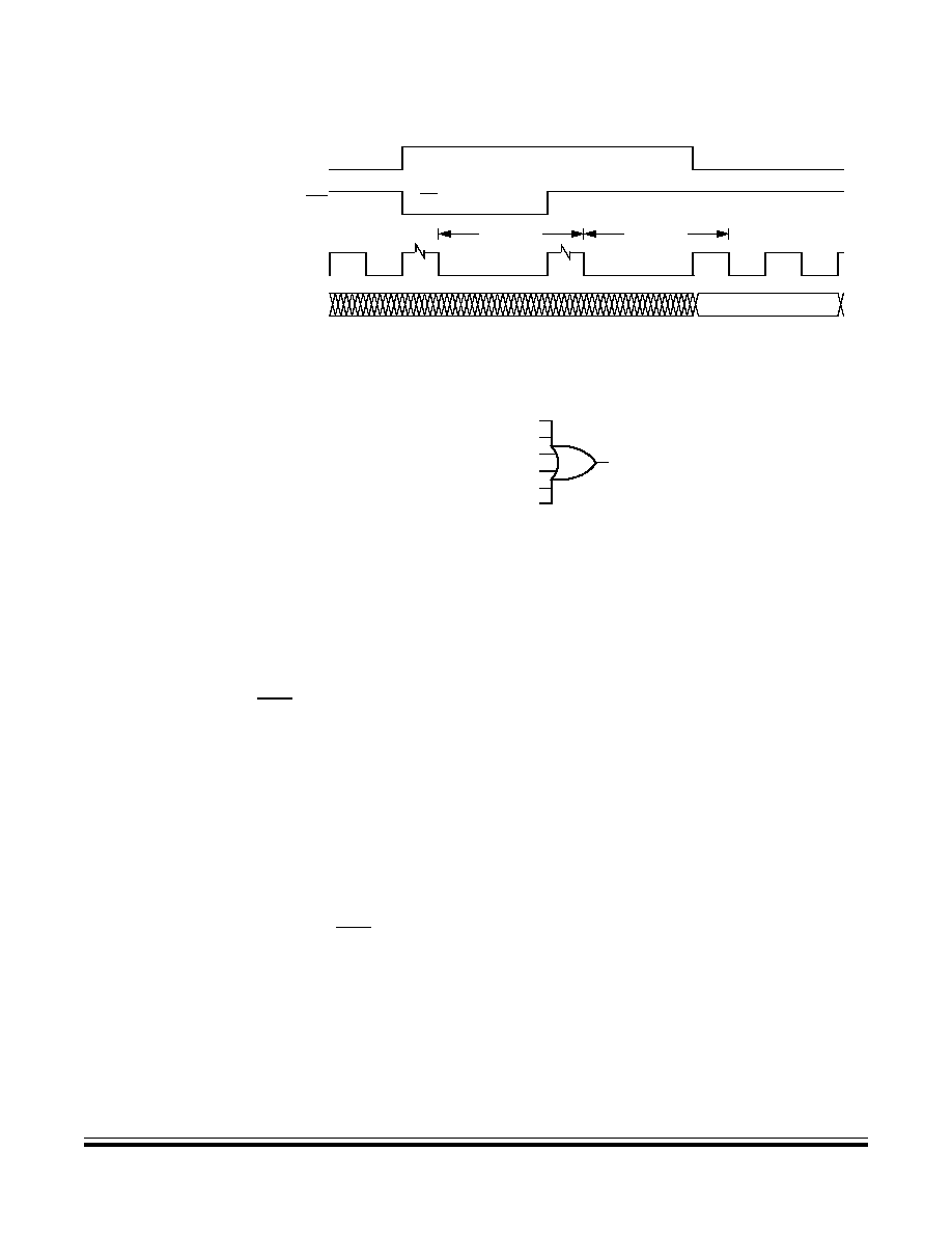
System Integration Module (SIM)
Reset and System Initialization
MC68HC908GR16 -- Rev. 1.0
Data Sheet
MOTOROLA
System Integration Module (SIM)
201
Figure 15-6. Internal Reset Timing
The COP reset is asynchronous to the bus clock.
Figure 15-7. Sources of Internal Reset
The active reset feature allows the part to issue a reset to peripherals and other
chips within a system built around the MCU.
15.3.2.1 Power-On Reset
When power is first applied to the MCU, the power-on reset module (POR)
generates a pulse to indicate that power-on has occurred. The external reset pin
(RST) is held low while the SIM counter counts out 4096 + 32 CGMXCLK cycles.
Thirty-two CGMXCLK cycles later, the CPU and memories are released from reset
to allow the reset vector sequence to occur.
At power-on, these events occur:
�
A POR pulse is generated.
�
The internal reset signal is asserted.
�
The SIM enables CGMOUT.
�
Internal clocks to the CPU and modules are held inactive for 4096
CGMXCLK cycles to allow stabilization of the oscillator.
�
The RST pin is driven low during the oscillator stabilization time.
�
The POR bit of the SIM reset status register (SRSR) is set and all other bits
in the register are cleared.
IRST
RST
RST PULLED LOW BY MCU
IAB
32 CYCLES
32 CYCLES
VECTOR HIGH
CGMXCLK
ILLEGAL ADDRESS RST
ILLEGAL OPCODE RST
COPRST
LVI
POR
INTERNAL RESET
MODRST

System Integration Module (SIM)
Data Sheet
MC68HC908GR16 -- Rev. 1.0
202
System Integration Module (SIM)
MOTOROLA
Figure 15-8. POR Recovery
15.3.2.2 Computer Operating Properly (COP) Reset
An input to the SIM is reserved for the COP reset signal. The overflow of the COP
counter causes an internal reset and sets the COP bit in the SIM reset status
register (SRSR). The SIM actively pulls down the RST pin for all internal reset
sources.
The COP module is disabled if the RST pin or the IRQ pin is held at V
TST
while the
MCU is in monitor mode. The COP module can be disabled only through
combinational logic conditioned with the high voltage signal on the RST or the IRQ
pin. This prevents the COP from becoming disabled as a result of external noise.
During a break state, V
TST
on the RST pin disables the COP module.
15.3.2.3 Illegal Opcode Reset
The SIM decodes signals from the CPU to detect illegal instructions. An illegal
instruction sets the ILOP bit in the SIM reset status register (SRSR) and causes a
reset.
If the stop enable bit, STOP, in the mask option register is logic 0, the SIM treats
the STOP instruction as an illegal opcode and causes an illegal opcode reset. The
SIM actively pulls down the RST pin for all internal reset sources.
15.3.2.4 Illegal Address Reset
An opcode fetch from an unmapped address generates an illegal address reset.
The SIM verifies that the CPU is fetching an opcode prior to asserting the ILAD bit
in the SIM reset status register (SRSR) and resetting the MCU. A data fetch from
an unmapped address does not generate a reset. The SIM actively pulls down the
RST pin for all internal reset sources.
PORRST
OSC1
CGMXCLK
CGMOUT
RST
IAB
4096
CYCLES
32
CYCLES
$FFFE
$FFFF

System Integration Module (SIM)
SIM Counter
MC68HC908GR16 -- Rev. 1.0
Data Sheet
MOTOROLA
System Integration Module (SIM)
203
15.3.2.5 Low-Voltage Inhibit (LVI) Reset
The low-voltage inhibit module (LVI) asserts its output to the SIM when the V
DD
voltage falls to the LVI
TRIPF
voltage. The LVI bit in the SIM reset status register
(SRSR) is set, and the external reset pin (RST) is held low while the SIM counter
counts out 4096 + 32 CGMXCLK cycles.
Thirty-two CGMXCLK cycles later, the CPU is released from reset to allow the
reset vector sequence to occur. The SIM actively pulls down the RST pin for all
internal reset sources.
15.3.2.6 Monitor Mode Entry Module Reset (MODRST)
The monitor mode entry module reset (MODRST) asserts its output to the SIM
when monitor mode is entered in the condition where the reset vectors are erased
($FF) (see
19.3.1.1 Normal Monitor Mode
). When MODRST gets asserted, an
internal reset occurs. The SIM actively pulls down the RST pin for all internal reset
sources.
15.4 SIM Counter
The SIM counter is used by the power-on reset module (POR) and in stop mode
recovery to allow the oscillator time to stabilize before enabling the internal bus
(IBUS) clocks. The SIM counter is 13 bits long.
15.4.1 SIM Counter During Power-On Reset
The power-on reset module (POR) detects power applied to the MCU. At
power-on, the POR circuit asserts the signal PORRST. Once the SIM is initialized,
it enables the clock generation module (CGM) to drive the bus clock state machine.
15.4.2 SIM Counter During Stop Mode Recovery
The SIM counter also is used for stop mode recovery. The STOP instruction clears
the SIM counter. After an interrupt, break, or reset, the SIM senses the state of the
short stop recovery bit, SSREC, in the mask option register. If the SSREC bit is a
logic 1, then the stop recovery is reduced from the normal delay of 4096 CGMXCLK
cycles down to 32 CGMXCLK cycles. This is ideal for applications using canned
oscillators that do not require long startup times from stop mode. External crystal
applications should use the full stop recovery time, that is, with SSREC cleared.
15.4.3 SIM Counter and Reset States
External reset has no effect on the SIM counter. See
15.6.2 Stop Mode
for details.
The SIM counter is free-running after all reset states. See
15.3.2 Active Resets
from Internal Sources
for counter control and internal reset recovery sequences.
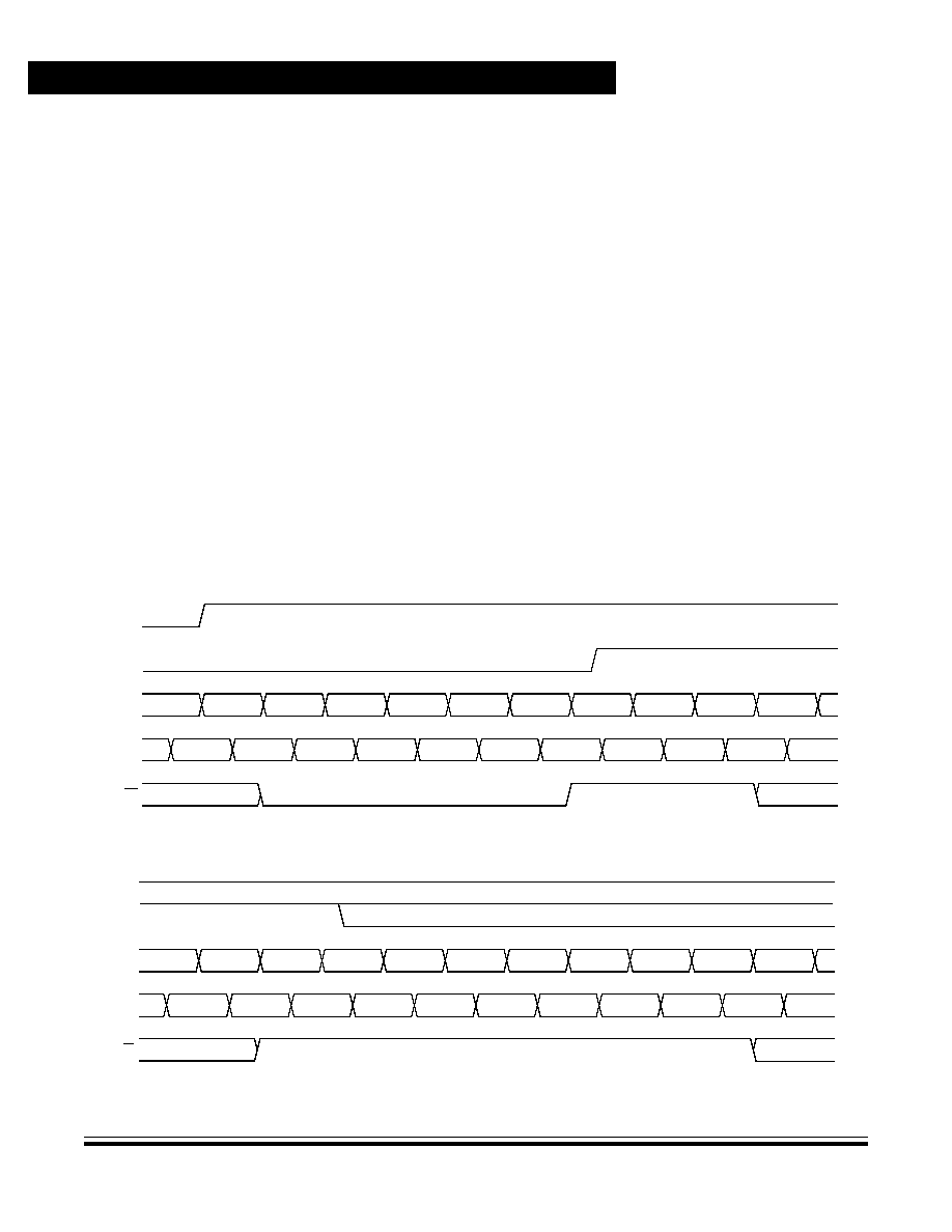
System Integration Module (SIM)
Data Sheet
MC68HC908GR16 -- Rev. 1.0
204
System Integration Module (SIM)
MOTOROLA
15.5 Exception Control
Normal, sequential program execution can be changed in three different ways:
�
Interrupts:
�
Maskable hardware CPU interrupts
�
Non-maskable software interrupt instruction (SWI)
�
Reset
�
Break interrupts
15.5.1 Interrupts
At the beginning of an interrupt, the CPU saves the CPU register contents on the
stack and sets the interrupt mask (I bit) to prevent additional interrupts. At the end
of an interrupt, the RTI instruction recovers the CPU register contents from the
stack so that normal processing can resume.
Figure 15-9
shows interrupt entry
timing.
Figure 15-10
shows interrupt recovery timing.
Interrupts are latched, and arbitration is performed in the SIM at the start of
interrupt processing. The arbitration result is a constant that the CPU uses to
determine which vector to fetch. Once an interrupt is latched by the SIM, no other
interrupt can take precedence, regardless of priority, until the latched interrupt is
serviced (or the I bit is cleared). See
Figure 15-11
.
Figure 15-9
.
Interrupt Entry Timing
Figure 15-10. Interrupt Recovery Timing
MODULE
IDB
R/W
INTERRUPT
DUMMY
SP
SP � 1
SP � 2
SP � 3
SP � 4
VECT H
VECT L
START ADDR
IAB
DUMMY
PC � 1[7:0] PC � 1[15:8]
X
A
CCR
V DATA H
V DATA L
OPCODE
I BIT
IDB
R/W
MODULE INTERRUPT
SP � 4
SP � 3
SP � 2
SP � 1
SP
PC
PC + 1
IAB
CCR
A
X
PC � 1 [7:0] PC � 1 [15:8] OPCODE
OPERAND
I BIT
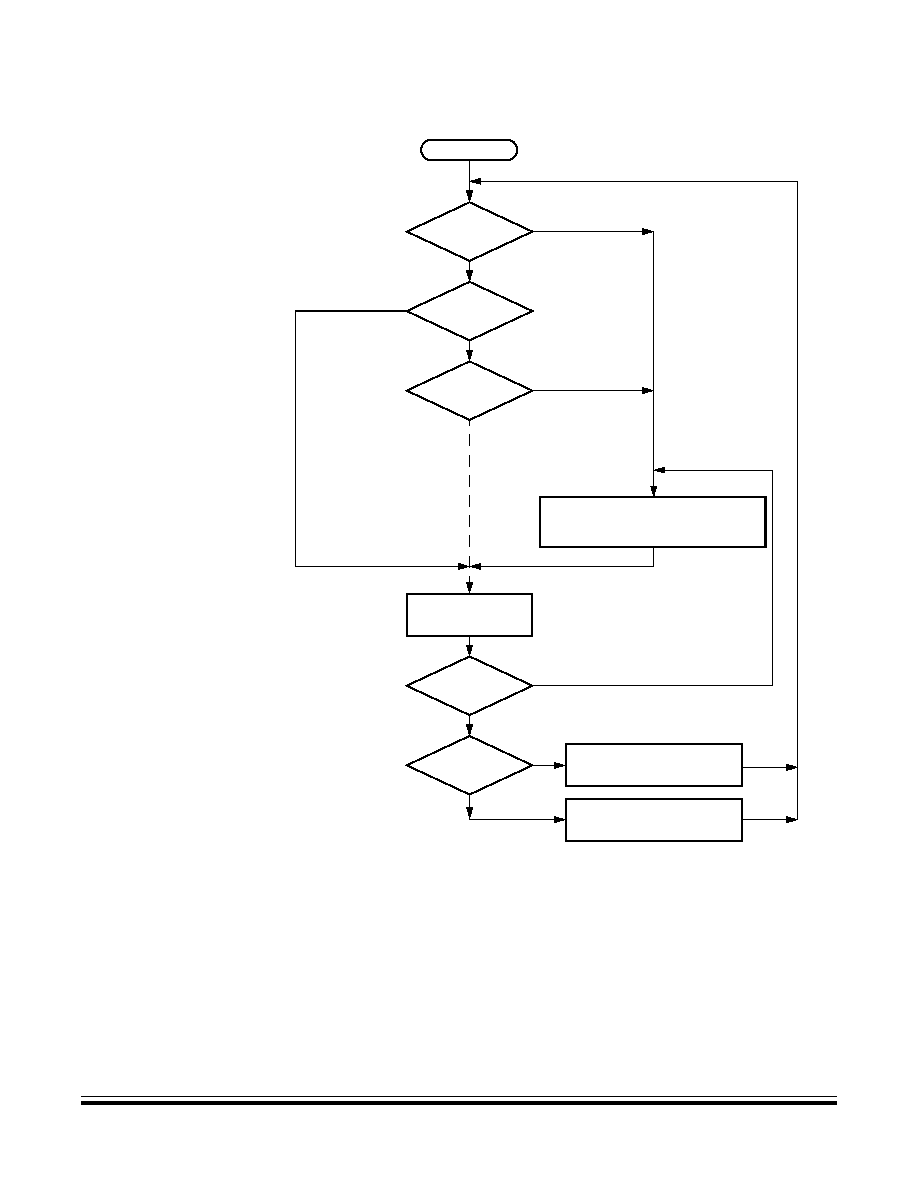
System Integration Module (SIM)
Exception Control
MC68HC908GR16 -- Rev. 1.0
Data Sheet
MOTOROLA
System Integration Module (SIM)
205
Figure 15-11. Interrupt Processing
NO
NO
YES
NO
NO
YES
NO
YES
AS MANY INTERRUPTS
I BIT SET?
FROM RESET
BREAK
I BIT SET?
IRQ
INTERRUPT?
SWI
INSTRUCTION?
RTI
INSTRUCTION?
FETCH NEXT
INSTRUCTION
UNSTACK CPU REGISTERS
STACK CPU REGISTERS
SET I BIT
LOAD PC WITH INTERRUPT VECTOR
EXECUTE INSTRUCTION
YES
YES
AS EXIST ON CHIP
INTERRUPT?
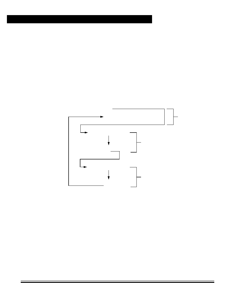
System Integration Module (SIM)
Data Sheet
MC68HC908GR16 -- Rev. 1.0
206
System Integration Module (SIM)
MOTOROLA
15.5.1.1 Hardware Interrupts
A hardware interrupt does not stop the current instruction. Processing of a
hardware interrupt begins after completion of the current instruction. When the
current instruction is complete, the SIM checks all pending hardware interrupts.
If interrupts are not masked (I bit clear in the condition code register) and if the
corresponding interrupt enable bit is set, the SIM proceeds with interrupt
processing; otherwise, the next instruction is fetched and executed.
If more than one interrupt is pending at the end of an instruction execution, the
highest priority interrupt is serviced first.
Figure 15-12
demonstrates what happens
when two interrupts are pending. If an interrupt is pending upon exit from the
original interrupt service routine, the pending interrupt is serviced before the LDA
instruction is executed.
Figure 15-12
.
Interrupt Recognition Example
The LDA opcode is prefetched by both the INT1 and INT2 RTI instructions.
However, in the case of the INT1 RTI prefetch, this is a redundant operation.
NOTE:
To maintain compatibility with the M6805 Family, the H register is not pushed on
the stack during interrupt entry. If the interrupt service routine modifies the H
register or uses the indexed addressing mode, software should save the H register
and then restore it prior to exiting the routine.
CLI
LDA
INT1
PULH
RTI
INT2
BACKGROUND
#$FF
PSHH
INT1 INTERRUPT SERVICE ROUTINE
PULH
RTI
PSHH
INT2 INTERRUPT SERVICE ROUTINE
ROUTINE
System Integration Module (SIM)
Exception Control
MC68HC908GR16 -- Rev. 1.0
Data Sheet
MOTOROLA
System Integration Module (SIM)
207
15.5.1.2 SWI Instruction
The SWI instruction is a non-maskable instruction that causes an interrupt
regardless of the state of the interrupt mask (I bit) in the condition code register.
NOTE:
A software interrupt pushes PC onto the stack. A software interrupt does not push
PC � 1, as a hardware interrupt does.
15.5.1.3 Interrupt Status Registers
The flags in the interrupt status registers identify maskable interrupt sources.
Table
15-3
summarizes the interrupt sources and the interrupt status register flags that
they set. The interrupt status registers can be useful for debugging.
Table 15-3. Interrupt Sources
Priority
Interrupt Source
Interrupt Status Register Flag
Highest
Reset
--
SWI instruction
--
IRQ pin
I1
ICG clock monitor
I2
TIM1 channel 0
I3
TIM1 channel 1
I4
TIM1 overflow
I5
TIM2 channel 0
I6
TIM2 channel 1
I7
TIM2 overflow
I8
SPI receiver full
I9
SPI transmitter empty
I10
SCI receive error
I11
SCI receive
I12
SCI transmit
I13
Keyboard
I14
ADC conversion complete
I15
Lowest
Timebase module
I16

System Integration Module (SIM)
Data Sheet
MC68HC908GR16 -- Rev. 1.0
208
System Integration Module (SIM)
MOTOROLA
Interrupt Status
Register 1
I6�I1 -- Interrupt Flags 1�6
These flags indicate the presence of interrupt requests from the sources shown
in
Table 15-3
.
1 = Interrupt request present
0 = No interrupt request present
Bit 0 and Bit 1 -- Always read 0
Interrupt Status
Register 2
I14�I7 -- Interrupt Flags 14�7
These flags indicate the presence of interrupt requests from the sources shown
in
Table 15-3
.
1 = Interrupt request present
0 = No interrupt request present
Interrupt Status
Register 3
Bits 7�6 -- Always read 0
I20�I15 -- Interrupt Flags 20�15
These flags indicate the presence of an interrupt request from the source shown
in
Table 15-3
.
1 = Interrupt request present
0 = No interrupt request present
Address:
$FE04
Bit 7
6
5
4
3
2
1
Bit 0
Read:
I6
I5
I4
I3
I2
I1
0
0
Write:
R
R
R
R
R
R
R
R
Reset:
0
0
0
0
0
0
0
0
R
= Reserved
Figure 15-13. Interrupt Status Register 1 (INT1)
Address:
$FE05
Bit 7
6
5
4
3
2
1
Bit 0
Read:
I14
I13
I12
I11
I10
I9
I8
I7
Write:
R
R
R
R
R
R
R
R
Reset:
0
0
0
0
0
0
0
0
R
= Reserved
Figure 15-14. Interrupt Status Register 2 (INT2)
Address:
$FE06
Bit 7
6
5
4
3
2
1
Bit 0
Read:
0
0
I20
I19
I18
I17
I16
I15
Write:
R
R
R
R
R
R
R
R
Reset:
0
0
0
0
0
0
0
0
R
= Reserved
Figure 15-15. Interrupt Status Register 3 (INT3)

System Integration Module (SIM)
Low-Power Modes
MC68HC908GR16 -- Rev. 1.0
Data Sheet
MOTOROLA
System Integration Module (SIM)
209
15.5.2 Reset
All reset sources always have equal and highest priority and cannot be arbitrated.
15.5.3 Break Interrupts
The break module can stop normal program flow at a software-programmable
break point by asserting its break interrupt output (see
Section 18. Timer
Interface Module (TIM)
). The SIM puts the CPU into the break state by forcing it
to the SWI vector location. Refer to the break interrupt subsection of each module
to see how each module is affected by the break state.
15.5.4 Status Flag Protection in Break Mode
The SIM controls whether status flags contained in other modules can be cleared
during break mode. The user can select whether flags are protected from being
cleared by properly initializing the break clear flag enable bit (BCFE) in the SIM
break flag control register (SBFCR).
Protecting flags in break mode ensures that set flags will not be cleared while in
break mode. This protection allows registers to be freely read and written during
break mode without losing status flag information.
Setting the BCFE bit enables the clearing mechanisms. Once cleared in break
mode, a flag remains cleared even when break mode is exited. Status flags with a
2-step clearing mechanism -- for example, a read of one register followed by the
read or write of another -- are protected, even when the first step is accomplished
prior to entering break mode. Upon leaving break mode, execution of the second
step will clear the flag as normal.
15.6 Low-Power Modes
Executing the WAIT or STOP instruction puts the MCU in a low
power-consumption mode for standby situations. The SIM holds the CPU in a
non-clocked state. The operation of each of these modes is described in the
following subsections. Both STOP and WAIT clear the interrupt mask (I) in the
condition code register, allowing interrupts to occur.
15.6.1 Wait Mode
In wait mode, the CPU clocks are inactive while the peripheral clocks continue to
run.
Figure 15-16
shows the timing for wait mode entry.
A module that is active during wait mode can wakeup the CPU with an interrupt if
the interrupt is enabled. Stacking for the interrupt begins one cycle after the WAIT
instruction during which the interrupt occurred. In wait mode, the CPU clocks are
inactive. Refer to the wait mode subsection of each module to see if the module is
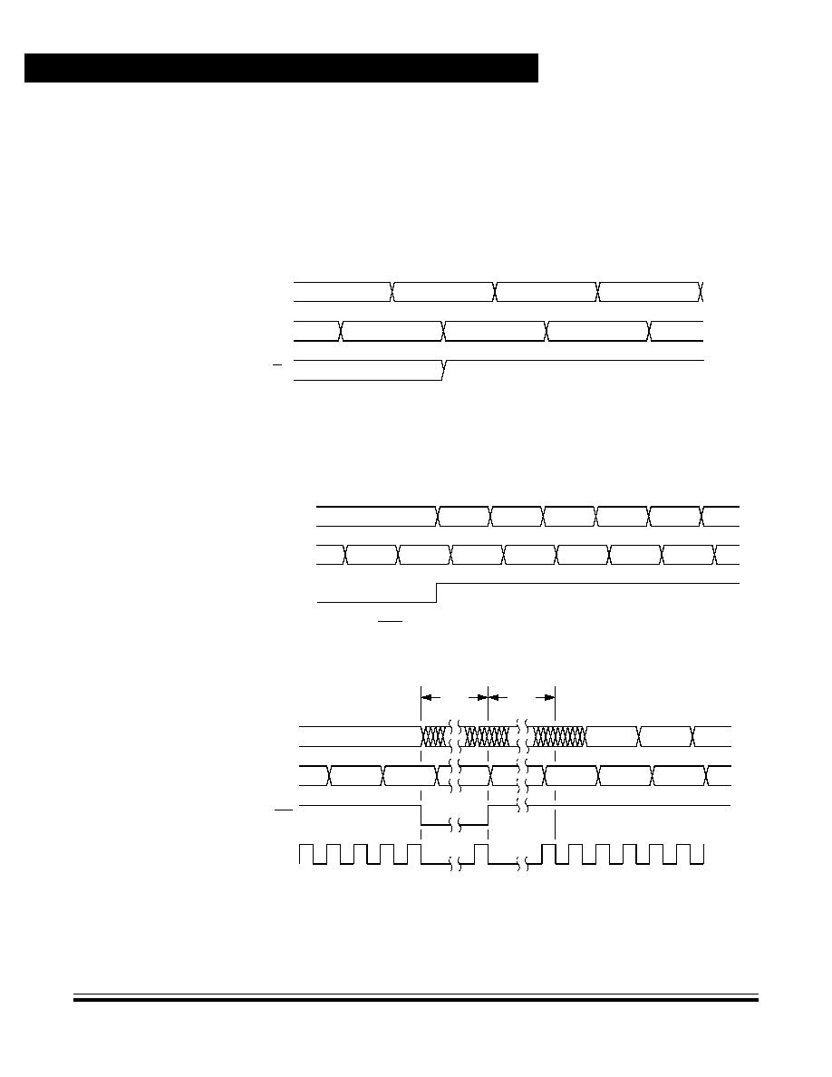
System Integration Module (SIM)
Data Sheet
MC68HC908GR16 -- Rev. 1.0
210
System Integration Module (SIM)
MOTOROLA
active or inactive in wait mode. Some modules can be programmed to be active in
wait mode.
Wait mode also can be exited by a reset (or break in emulation mode). A break
interrupt during wait mode sets the SIM break stop/wait bit, SBSW, in the SIM
break status register (SBSR). If the COP disable bit, COPD, in the mask option
register is logic 0, then the computer operating properly module (COP) is enabled
and remains active in wait mode.
Figure 15-16. Wait Mode Entry Timing
Figure 15-17
and
Figure 15-18
show the timing for WAIT recovery.
Figure 15-17. Wait Recovery from Interrupt
Figure 15-18. Wait Recovery from Internal Reset
WAIT ADDR + 1
SAME
SAME
IAB
IDB
PREVIOUS DATA
NEXT OPCODE
SAME
WAIT ADDR
SAME
R/W
Note: Previous data can be operand data or the WAIT opcode, depending on the
last instruction.
$6E0C
$6E0B
$00FF
$00FE
$00FD
$00FC
$A6
$A6
$01
$0B
$6E
$A6
IAB
IDB
EXITSTOPWAIT
Note: EXITSTOPWAIT = RST pin or CPU interrupt
IAB
IDB
RST
$A6
$A6
$6E0B
RST VCT H
RST VCT L
$A6
CGMXCLK
32
CYCLES
32
CYCLES
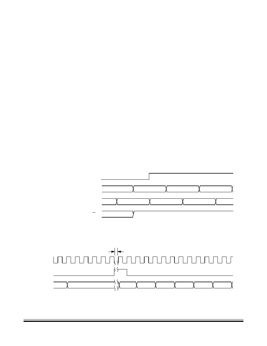
System Integration Module (SIM)
Low-Power Modes
MC68HC908GR16 -- Rev. 1.0
Data Sheet
MOTOROLA
System Integration Module (SIM)
211
15.6.2 Stop Mode
In stop mode, the SIM counter is reset and the system clocks are disabled. An
interrupt request from a module can cause an exit from stop mode. Stacking for
interrupts begins after the selected stop recovery time has elapsed. Reset also
causes an exit from stop mode.
The SIM disables the clock generator module outputs (CGMOUT and CGMXCLK)
in stop mode, stopping the CPU and peripherals. Stop recovery time is selectable
using the SSREC bit in the mask option register (MOR). If SSREC is set, stop
recovery is reduced from the normal delay of 4096 CGMXCLK cycles down to 32.
This is ideal for applications using canned oscillators that do not require long
startup times from stop mode.
NOTE:
External crystal applications should use the full stop recovery time by clearing the
SSREC bit.
The SIM counter is held in reset from the execution of the STOP instruction until
the beginning of stop recovery. It is then used to time the recovery period.
Figure
15-19
shows stop mode entry timing.
Figure 15-20
shows stop mode recovery time
from interrupt.
NOTE:
To minimize stop current, all pins configured as inputs should be driven to a logic
1 or logic 0.
Figure 15-19. Stop Mode Entry Timing
Figure 15-20. Stop Mode Recovery from Interrupt
STOP ADDR + 1
SAME
SAME
IAB
IDB
PREVIOUS DATA
NEXT OPCODE
SAME
STOP ADDR
SAME
R/W
CPUSTOP
Note: Previous data can be operand data or the STOP opcode, depending
on the last instruction.
CGMXCLK
INT/BREAK
IAB
STOP + 2
STOP + 2
SP
SP � 1
SP � 2
SP � 3
STOP +1
STOP RECOVERY PERIOD

System Integration Module (SIM)
Data Sheet
MC68HC908GR16 -- Rev. 1.0
212
System Integration Module (SIM)
MOTOROLA
15.7 SIM Registers
The SIM has three memory-mapped registers.
Table 15-4
shows the mapping of
these registers.
15.7.1 Break Status Register
The break status register (BSR) contains a flag to indicate that a break caused an
exit from wait mode. This register is only used in emulation mode.
SBSW -- SIM Break Stop/Wait
This status bit is useful in applications requiring a return to wait mode after
exiting from a break interrupt. Clear SBSW by writing a logic 0 to it. Reset clears
SBSW.
1 = Wait mode was exited by break interrupt.
0 = Wait mode was not exited by break interrupt.
SBSW can be read within the break state SWI routine. The user can modify the
return address on the stack by subtracting one from it.
Table 15-4. SIM Registers
Address
Register
Access Mode
$FE00
BSR
User
$FE01
SRSR
User
$FE03
BFCR
User
Address:
$FE00
Bit 7
6
5
4
3
2
1
Bit 0
Read:
R
R
R
R
R
R
SBSW
R
Write:
Note
(1)
Reset:
0
0
0
0
0
0
0
0
R
= Reserved
1. Writing a logic 0 clears SBSW.
Figure 15-21. Break Status Register (BSR)

System Integration Module (SIM)
SIM Registers
MC68HC908GR16 -- Rev. 1.0
Data Sheet
MOTOROLA
System Integration Module (SIM)
213
15.7.2 SIM Reset Status Register
This register contains six flags that show the source of the last reset provided all
previous reset status bits have been cleared. Clear the SIM reset status register by
reading it. A power-on reset sets the POR bit and clears all other bits in the register.
POR -- Power-On Reset Bit
1 = Last reset caused by POR circuit
0 = Read of SRSR
PIN -- External Reset Bit
1 = Last reset caused by external reset pin (RST)
0 = POR or read of SRSR
COP -- Computer Operating Properly Reset Bit
1 = Last reset caused by COP counter
0 = POR or read of SRSR
ILOP -- Illegal Opcode Reset Bit
1 = Last reset caused by an illegal opcode
0 = POR or read of SRSR
ILAD -- Illegal Address Reset Bit (opcode fetches only)
1 = Last reset caused by an opcode fetch from an illegal address
0 = POR or read of SRSR
MODRST -- Monitor Mode Entry Module Reset Bit
1 = Last reset caused by monitor mode entry when vector locations $FFFE
and $FFFF are $FF after POR while IRQ = V
DD
0 = POR or read of SRSR
LVI -- Low-Voltage Inhibit Reset Bit
1 = Last reset caused by the LVI circuit
0 = POR or read of SRSR
Address:
$FE01
Bit 7
6
5
4
3
2
1
Bit 0
Read:
POR
PIN
COP
ILOP
ILAD
MODRST
LVI
0
Write:
Reset:
1
0
0
0
0
0
0
0
= Unimplemented
Figure 15-22. SIM Reset Status Register (SRSR)

System Integration Module (SIM)
Data Sheet
MC68HC908GR16 -- Rev. 1.0
214
System Integration Module (SIM)
MOTOROLA
15.7.3 Break Flag Control Register
The break control register (BFCR) contains a bit that enables software to clear
status bits while the MCU is in a break state.
BCFE -- Break Clear Flag Enable Bit
This read/write bit enables software to clear status bits by accessing status
registers while the MCU is in a break state. To clear status bits during the break
state, the BCFE bit must be set.
1 = Status bits clearable during break
0 = Status bits not clearable during break
Address:
$FE03
Bit 7
6
5
4
3
2
1
Bit 0
Read:
BCFE
R
R
R
R
R
R
R
Write:
Reset:
0
R
= Reserved
Figure 15-23. Break Flag Control Register (BFCR)

MC68HC908GR16 -- Rev. 1.0
Data Sheet
MOTOROLA
Serial Peripheral Interface (SPI) Module
215
Data Sheet -- MC68HC908GR16
Section 16. Serial Peripheral Interface (SPI) Module
16.1 Introduction
This section describes the serial peripheral interface (SPI) module, which allows
full-duplex, synchronous, serial communications with peripheral devices.
16.2 Features
Features of the SPI module include:
�
Full-duplex operation
�
Master and slave modes
�
Double-buffered operation with separate transmit and receive registers
�
Four master mode frequencies (maximum = bus frequency
�
2)
�
Maximum slave mode frequency = bus frequency
�
Serial clock with programmable polarity and phase
�
Two separately enabled interrupts:
�
SPRF (SPI receiver full)
�
SPTE (SPI transmitter empty)
�
Mode fault error flag with CPU interrupt capability
�
Overflow error flag with CPU interrupt capability
�
Programmable wired-OR mode
�
I
2
C (inter-integrated circuit) compatibility
�
I/O (input/output) port bit(s) software configurable with pullup device(s) if
configured as input port bit(s)

Data Sheet
MC6
8
HC90
8
GR16 --
Re
v. 1.0
216
Se
ri
al Periph
eral Interfa
c
e (SPI)
Mo
dule
M
OTOROLA
Serial P
e
ripheral In
terface (SPI) Module
Figure 16-1. Block Diagram Highlighting SPI Block and Pins
MONITOR MODULE
M68HC08 CPU
CONTROL AND STATUS REGISTERS -- 64 BYTES
USER FLASH -- 15,872 BYTES
USER RAM -- 1024 BYTES
MONITOR ROM -- 350 BYTES
USER FLASH VECTOR SPACE -- 44 BYTES
PORTA
D
DRA
DDRC
PO
R
T
C
DDR
D
PORTD
DDRE
POR
T
E
INTERNAL BUS
OSC1
OSC2
RST
(3)
IRQ
(3)
PTA7/KBD7�PTA0/KBD0
(1)
PTB7/AD7
PTB6/AD6
PTB5/AD5
PTB4/AD4
PTB3/AD3
PTB2/AD2
PTB1/AD1
PTB0/AD0
PTC6
(1)
PTC5
(1)
PTC4
(1), (2)
PTC3
(1), (2)
PTC2
(1), (2)
PTC1
(1), (2)
PTC0
(1), (2)
PTD7/T2CH1
(1)
PTD6/T2CH0
(1)
PTD5/T1CH1
(1)
PTD4/T1CH0
(1)
PTD3/SPSCK
(1)
PTD2/MOSI
(1)
PTD1/MISO
(1)
PTD0/SS
(1)
PTE1/RxD
PTE0/TxD
SECURITY
MODULE
POWER
V
SS
V
DD
V
SSA
V
DDA
1. Ports are software configurable with pullup device if input port.
2. Higher current drive port pins
3. Pin contains integrated pullup device
MONITOR MODE ENTRY
MODULE
DDRB
PORTB
V
DDAD
/V
REFH
V
DDAD
/V
REFL
PTE5�PTE2
FLASH PROGRAMMING ROUTINES ROM -- 406 BYTES
CLOCK GENERATOR MODULE
CGMXFC
PHASE LOCKED LOOP
32�100 kHz OSCILLATOR
CPU
REGISTERS
ARITHMETIC/LOGIC
UNIT (ALU)
SYSTEM INTEGRATION
MODULE
SINGLE EXTERNAL
INTERRUPT MODULE
10-BIT ANALOG-TO-DIGITAL
CONVERTER MODULE
POWER-ON RESET
MODULE
PROGRAMMABLE TIMEBASE
MODULE
SINGLE BREAKPOINT
BREAK MODULE
DUAL VOLTAGE
LOW-VOLTAGE INHIBIT
MODULE
8-BIT KEYBOARD
INTERRUPT MODULE
2-CHANNEL TIMER
INTERFACE MODULE 1
2-CHANNEL TIMER
INTERFACE MODULE 2
ENHANCED SERIAL
COMUNICATIONS
INTERFACE MODULE
COMPUTER OPERATING
PROPERLY MODULE
SERIAL PERIPHERAL
INTERFACE MODULE
DATA BUS SWITCH
MODULE
MEMORY MAP
MODULE
CONFIGURATION
REGISTER 1�2
MODULE
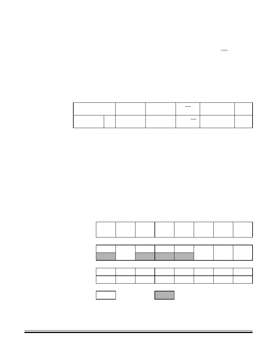
Serial Peripheral Interface (SPI) Module
Pin Name Conventions
MC68HC908GR16 -- Rev. 1.0
Data Sheet
MOTOROLA
Serial Peripheral Interface (SPI) Module
217
16.3 Pin Name Conventions
The text that follows describes the SPI. The SPI I/O pin names are SS (slave
select), SPSCK (SPI serial clock), CGND (clock ground), MOSI (master out slave
in), and MISO (master in/slave out). The SPI shares four I/O pins with four parallel
I/O ports.
The full names of the SPI I/O pins are shown in
Table 16-1
. The generic pin names
appear in the text that follows.
.
16.4 Functional Description
Figure 16-2
summarizes the SPI I/O registers and
Figure 16-3
shows the structure
of the SPI module.
The SPI module allows full-duplex, synchronous, serial communication between
the MCU and peripheral devices, including other MCUs. Software can poll the SPI
status flags or SPI operation can be interrupt driven.
If a port bit is configured for input, then an internal pullup device may be enabled
for that port bit. See
12.4.3 Port C Input Pullup Enable Register
.
The following paragraphs describe the operation of the SPI module.
Table 16-1. Pin Name Conventions
SPI Generic
Pin Names:
MISO
MOSI
SS
SPSCK
CGND
Full SPI
Pin Names:
SPI
PTD1/MISO
PTD2/MOSI
PTD0/SS
PTD3/SPSCK
V
SS
Addr.
Register Name
Bit 7
6
5
4
3
2
1
Bit 0
$0010
SPI Control Register
(SPCR)
See page 235.
Read:
SPRIE
R
SPMSTR
CPOL
CPHA
SPWOM
SPE
SPTIE
Write:
Reset:
0
0
1
0
1
0
0
0
$0011
SPI Status and Control
Register (SPSCR)
See page 236.
Read:
SPRF
ERRIE
OVRF
MODF
SPTE
MODFEN
SPR1
SPR0
Write:
Reset:
0
0
0
0
1
0
0
0
$0012
SPI Data Register
(SPDR)
See page 238.
Read:
R7
R6
R5
R4
R3
R2
R1
R0
Write:
T7
T6
T5
T4
T3
T2
T1
T0
Reset:
Unaffected by reset
R
= Reserved
= Unimplemented
Figure 16-2. SPI I/O Register Summary
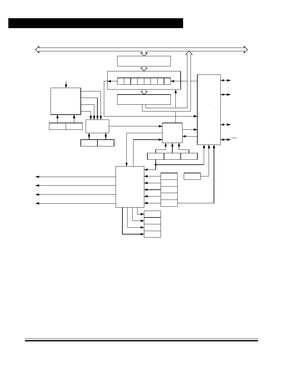
Serial Peripheral Interface (SPI) Module
Data Sheet
MC68HC908GR16 -- Rev. 1.0
218
Serial Peripheral Interface (SPI) Module
MOTOROLA
Figure 16-3. SPI Module Block Diagram
TRANSMITTER CPU INTERRUPT REQUEST
RESERVED
RECEIVER/ERROR CPU INTERRUPT REQUEST
7
6
5
4
3
2
1
0
SPR1
SPMSTR
TRANSMIT DATA REGISTER
SHIFT REGISTER
SPR0
CGMOUT
� 2
CLOCK
SELECT
� 2
CLOCK
DIVIDER
� 8
� 32
� 128
CLOCK
LOGIC
CPHA
CPOL
SPI
SPRIE
SPE
SPWOM
SPRF
SPTE
OVRF
RESERVED
M
S
PIN
CONTROL
LOGIC
RECEIVE DATA REGISTER
SPTIE
SPE
INTERNAL BUS
FROM SIM
MODFEN
ERRIE
CONTROL
MODF
SPMSTR
MOSI
MISO
SPSCK
SS
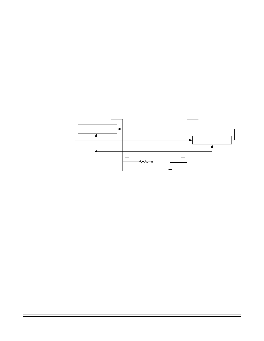
Serial Peripheral Interface (SPI) Module
Functional Description
MC68HC908GR16 -- Rev. 1.0
Data Sheet
MOTOROLA
Serial Peripheral Interface (SPI) Module
219
16.4.1 Master Mode
The SPI operates in master mode when the SPI master bit, SPMSTR, is set.
NOTE:
Configure the SPI modules as master or slave before enabling them. Enable the
master SPI before enabling the slave SPI. Disable the slave SPI before disabling
the master SPI. See
16.13.1 SPI Control Register
.
Only a master SPI module can initiate transmissions. Software begins the
transmission from a master SPI module by writing to the transmit data register. If
the shift register is empty, the byte immediately transfers to the shift register,
setting the SPI transmitter empty bit, SPTE. The byte begins shifting out on the
MOSI pin under the control of the serial clock. See
Figure 16-4
.
Figure 16-4. Full-Duplex Master-Slave Connections
The SPR1 and SPR0 bits control the baud rate generator and determine the speed
of the shift register. (See
16.13.2 SPI Status and Control Register
.) Through the
SPSCK pin, the baud rate generator of the master also controls the shift register of
the slave peripheral.
As the byte shifts out on the MOSI pin of the master, another byte shifts in from the
slave on the master's MISO pin. The transmission ends when the receiver full bit,
SPRF, becomes set. At the same time that SPRF becomes set, the byte from the
slave transfers to the receive data register. In normal operation, SPRF signals the
end of a transmission. Software clears SPRF by reading the SPI status and control
register with SPRF set and then reading the SPI data register. Writing to the SPI
data register clears the SPTE bit.
SHIFT REGISTER
SHIFT REGISTER
BAUD RATE
GENERATOR
MASTER MCU
SLAVE MCU
V
DD
MOSI
MOSI
MISO
MISO
SPSCK
SPSCK
SS
SS

Serial Peripheral Interface (SPI) Module
Data Sheet
MC68HC908GR16 -- Rev. 1.0
220
Serial Peripheral Interface (SPI) Module
MOTOROLA
16.4.2 Slave Mode
The SPI operates in slave mode when the SPMSTR bit is clear. In slave mode, the
SPSCK pin is the input for the serial clock from the master MCU. Before a data
transmission occurs, the SS pin of the slave SPI must be at logic 0. SS must remain
low until the transmission is complete. See
16.7.2 Mode Fault Error
.
In a slave SPI module, data enters the shift register under the control of the serial
clock from the master SPI module. After a byte enters the shift register of a slave
SPI, it transfers to the receive data register, and the SPRF bit is set. To prevent an
overflow condition, slave software then must read the receive data register before
another full byte enters the shift register.
The maximum frequency of the SPSCK for an SPI configured as a slave is the bus
clock speed (which is twice as fast as the fastest master SPSCK clock that can be
generated). The frequency of the SPSCK for an SPI configured as a slave does not
have to correspond to any SPI baud rate. The baud rate only controls the speed of
the SPSCK generated by an SPI configured as a master. Therefore, the frequency
of the SPSCK for an SPI configured as a slave can be any frequency less than or
equal to the bus speed.
When the master SPI starts a transmission, the data in the slave shift register
begins shifting out on the MISO pin. The slave can load its shift register with a new
byte for the next transmission by writing to its transmit data register. The slave must
write to its transmit data register at least one bus cycle before the master starts the
next transmission. Otherwise, the byte already in the slave shift register shifts out
on the MISO pin. Data written to the slave shift register during a transmission
remains in a buffer until the end of the transmission.
When the clock phase bit (CPHA) is set, the first edge of SPSCK starts a
transmission. When CPHA is clear, the falling edge of SS starts a transmission.
See
16.5 Transmission Formats
.
NOTE:
SPSCK must be in the proper idle state before the slave is enabled to prevent
SPSCK from appearing as a clock edge.
16.5 Transmission Formats
During an SPI transmission, data is simultaneously transmitted (shifted out serially)
and received (shifted in serially). A serial clock synchronizes shifting and sampling
on the two serial data lines. A slave select line allows selection of an individual
slave SPI device; slave devices that are not selected do not interfere with SPI bus
activities. On a master SPI device, the slave select line can optionally be used to
indicate multiple-master bus contention.

Serial Peripheral Interface (SPI) Module
Transmission Formats
MC68HC908GR16 -- Rev. 1.0
Data Sheet
MOTOROLA
Serial Peripheral Interface (SPI) Module
221
16.5.1 Clock Phase and Polarity Controls
Software can select any of four combinations of serial clock (SPSCK) phase and
polarity using two bits in the SPI control register (SPCR). The clock polarity is
specified by the CPOL control bit, which selects an active high or low clock and has
no significant effect on the transmission format.
The clock phase (CPHA) control bit selects one of two fundamentally different
transmission formats. The clock phase and polarity should be identical for the
master SPI device and the communicating slave device. In some cases, the phase
and polarity are changed between transmissions to allow a master device to
communicate with peripheral slaves having different requirements.
NOTE:
Before writing to the CPOL bit or the CPHA bit, disable the SPI by clearing the SPI
enable bit (SPE).
16.5.2 Transmission Format When CPHA = 0
Figure 16-5
shows an SPI transmission in which CPHA is logic 0. The figure should
not be used as a replacement for data sheet parametric information.
Two waveforms are shown for SPSCK: one for CPOL = 0 and another for
CPOL = 1. The diagram may be interpreted as a master or slave timing diagram
since the serial clock (SPSCK), master in/slave out (MISO), and master out/slave
in (MOSI) pins are directly connected between the master and the slave. The MISO
signal is the output from the slave, and the MOSI signal is the output from the
master. The SS line is the slave select input to the slave. The slave SPI drives its
MISO output only when its slave select input (SS) is at logic 0, so that only the
selected slave drives to the master. The SS pin of the master is not shown but is
assumed to be inactive. The SS pin of the master must be high or must be
reconfigured as general-purpose I/O not affecting the SPI. (See
16.7.2 Mode Fault
Error
.) When CPHA = 0, the first SPSCK edge is the MSB capture strobe.
Therefore, the slave must begin driving its data before the first SPSCK edge, and
a falling edge on the SS pin is used to start the slave data transmission. The slave's
SS pin must be toggled back to high and then low again between each byte
transmitted as shown in
Figure 16-6
.
When CPHA = 0 for a slave, the falling edge of SS indicates the beginning of the
transmission. This causes the SPI to leave its idle state and begin driving the MISO
pin with the MSB of its data. Once the transmission begins, no new data is allowed
into the shift register from the transmit data register. Therefore, the SPI data
register of the slave must be loaded with transmit data before the falling edge of
SS. Any data written after the falling edge is stored in the transmit data register and
transferred to the shift register after the current transmission.
Serial Peripheral Interface (SPI) Module
Data Sheet
MC68HC908GR16 -- Rev. 1.0
222
Serial Peripheral Interface (SPI) Module
MOTOROLA
Figure 16-5. Transmission Format (CPHA = 0)
Figure 16-6. CPHA/SS Timing
16.5.3 Transmission Format When CPHA = 1
Figure 16-7
shows an SPI transmission in which CPHA is logic 1. The figure should
not be used as a replacement for data sheet parametric information. Two
waveforms are shown for SPSCK: one for CPOL = 0 and another for CPOL = 1.
The diagram may be interpreted as a master or slave timing diagram since the
serial clock (SPSCK), master in/slave out (MISO), and master out/slave in (MOSI)
pins are directly connected between the master and the slave. The MISO signal is
the output from the slave, and the MOSI signal is the output from the master. The
SS line is the slave select input to the slave. The slave SPI drives its MISO output
only when its slave select input (SS) is at logic 0, so that only the selected slave
drives to the master. The SS pin of the master is not shown but is assumed to be
inactive. The SS pin of the master must be high or must be reconfigured as
general-purpose I/O not affecting the SPI. (See
16.7.2 Mode Fault Error
.) When
CPHA = 1, the master begins driving its MOSI pin on the first SPSCK edge.
Therefore, the slave uses the first SPSCK edge as a start transmission signal. The
SS pin can remain low between transmissions. This format may be preferable in
systems having only one master and only one slave driving the MISO data line.
When CPHA = 1 for a slave, the first edge of the SPSCK indicates the beginning
of the transmission. This causes the SPI to leave its idle state and begin driving the
MISO pin with the MSB of its data. Once the transmission begins, no new data is
allowed into the shift register from the transmit data register. Therefore, the SPI
BIT 6
BIT 5
BIT 4
BIT 3
BIT 2
BIT 1
LSB
MSB
BIT 6
BIT 5
BIT 4
BIT 3
BIT 2
BIT 1
LSB
MSB
1
2
3
4
5
6
7
8
SPSCK CYCLE #
FOR REFERENCE
SPSCK; CPOL = 0
SPSCK; CPOL =1
MOSI
FROM MASTER
MISO
FROM SLAVE
SS; TO SLAVE
CAPTURE STROBE
BYTE 1
BYTE 3
MISO/MOSI
BYTE 2
MASTER SS
SLAVE SS
CPHA = 0
SLAVE SS
CPHA = 1
Serial Peripheral Interface (SPI) Module
Transmission Formats
MC68HC908GR16 -- Rev. 1.0
Data Sheet
MOTOROLA
Serial Peripheral Interface (SPI) Module
223
data register of the slave must be loaded with transmit data before the first edge of
SPSCK. Any data written after the first edge is stored in the transmit data register
and transferred to the shift register after the current transmission.
Figure 16-7. Transmission Format (CPHA = 1)
16.5.4 Transmission Initiation Latency
When the SPI is configured as a master (SPMSTR = 1), writing to the SPDR starts
a transmission. CPHA has no effect on the delay to the start of the transmission,
but it does affect the initial state of the SPSCK signal. When CPHA = 0, the SPSCK
signal remains inactive for the first half of the first SPSCK cycle. When CPHA = 1,
the first SPSCK cycle begins with an edge on the SPSCK line from its inactive to
its active level. The SPI clock rate (selected by SPR1:SPR0) affects the delay from
the write to SPDR and the start of the SPI transmission. (See
Figure 16-8
.) The
internal SPI clock in the master is a free-running derivative of the internal MCU
clock. To conserve power, it is enabled only when both the SPE and SPMSTR bits
are set. SPSCK edges occur halfway through the low time of the internal MCU
clock. Since the SPI clock is free-running, it is uncertain where the write to the
SPDR occurs relative to the slower SPSCK. This uncertainty causes the variation
in the initiation delay shown in
Figure 16-8
. This delay is no longer than a single
SPI bit time. That is, the maximum delay is two MCU bus cycles for DIV2, eight
MCU bus cycles for DIV8, 32 MCU bus cycles for DIV32, and 128 MCU bus cycles
for DIV128.
BIT 6
BIT 5
BIT 4
BIT 3
BIT 2
BIT 1
LSB
MSB
BIT 6
BIT 5
BIT 4
BIT 3
BIT 2
BIT 1
LSB
MSB
1
2
3
4
5
6
7
8
SPSCK CYCLE #
FOR REFERENCE
SPSCK; CPOL = 0
SPSCK; CPOL =1
MOSI
FROM MASTER
MISO
FROM SLAVE
SS; TO SLAVE
CAPTURE STROBE
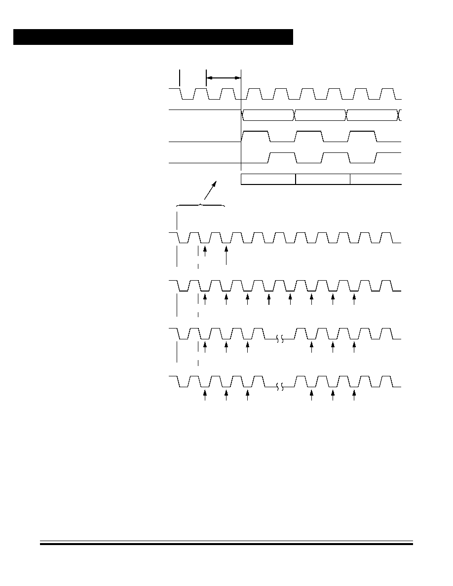
Serial Peripheral Interface (SPI) Module
Data Sheet
MC68HC908GR16 -- Rev. 1.0
224
Serial Peripheral Interface (SPI) Module
MOTOROLA
Figure 16-8. Transmission Start Delay (Master)
WRITE
TO SPDR
INITIATION DELAY
BUS
MOSI
SPSCK
CPHA = 1
SPSCK
CPHA = 0
SPSCK CYCLE
NUMBER
MSB
BIT 6
1
2
CLOCK
WRITE
TO SPDR
EARLIEST
LATEST
SPSCK = INTERNAL CLOCK
� 2;
EARLIEST
LATEST
2 POSSIBLE START POINTS
SPSCK = INTERNAL CLOCK
� 8;
8 POSSIBLE START POINTS
EARLIEST
LATEST
SPSCK = INTERNAL CLOCK
� 32;
32 POSSIBLE START POINTS
EARLIEST
LATEST
SPSCK = INTERNAL CLOCK
� 128;
128 POSSIBLE START POINTS
WRITE
TO SPDR
WRITE
TO SPDR
WRITE
TO SPDR
BUS
CLOCK
BIT 5
3
BUS
CLOCK
BUS
CLOCK
BUS
CLOCK
INITIATION DELAY FROM WRITE SPDR TO TRANSFER BEGIN
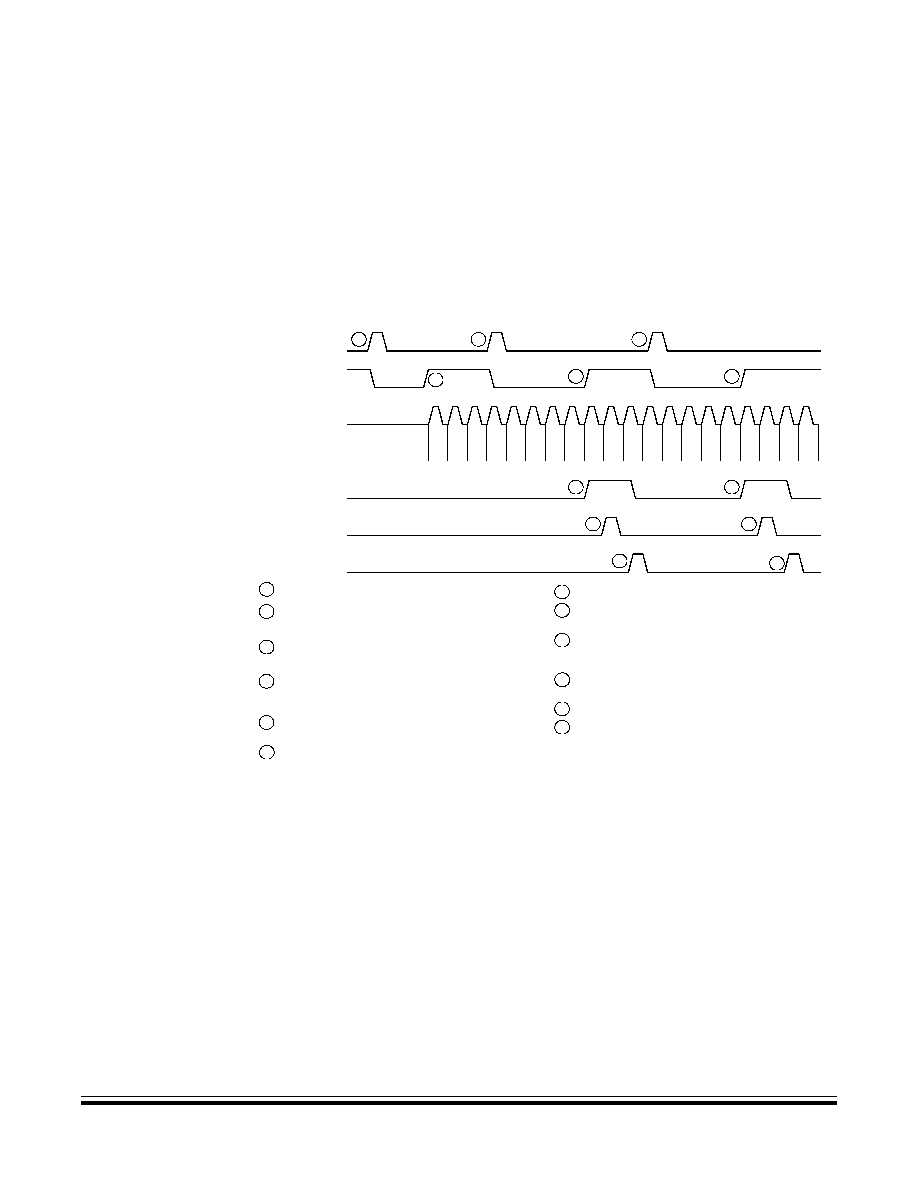
Serial Peripheral Interface (SPI) Module
Queuing Transmission Data
MC68HC908GR16 -- Rev. 1.0
Data Sheet
MOTOROLA
Serial Peripheral Interface (SPI) Module
225
16.6 Queuing Transmission Data
The double-buffered transmit data register allows a data byte to be queued and
transmitted. For an SPI configured as a master, a queued data byte is transmitted
immediately after the previous transmission has completed. The SPI transmitter
empty flag (SPTE) indicates when the transmit data buffer is ready to accept new
data. Write to the transmit data register only when the SPTE bit is high.
Figure 16-9
shows the timing associated with doing back-to-back transmissions with the SPI
(SPSCK has CPHA: CPOL = 1:0).
Figure 16-9. SPRF/SPTE CPU Interrupt Timing
The transmit data buffer allows back-to-back transmissions without the slave
precisely timing its writes between transmissions as in a system with a single data
buffer. Also, if no new data is written to the data buffer, the last value contained in
the shift register is the next data word to be transmitted.
For an idle master or idle slave that has no data loaded into its transmit buffer, the
SPTE is set again no more than two bus cycles after the transmit buffer empties
into the shift register. This allows the user to queue up a 16-bit value to send. For
an already active slave, the load of the shift register cannot occur until the
transmission is completed. This implies that a back-to-back write to the transmit
data register is not possible. The SPTE indicates when the next write can occur.
BIT
3
MOSI
SPSCK
SPTE
WRITE TO SPDR
1
CPU WRITES BYTE 2 TO SPDR, QUEUEING BYTE 2
CPU WRITES BYTE 1 TO SPDR, CLEARING SPTE BIT.
BYTE 1 TRANSFERS FROM TRANSMIT DATA
3
1
2
2
3
5
REGISTER TO SHIFT REGISTER, SETTING SPTE BIT.
SPRF
READ SPSCR
MSB BIT
6
BIT
5
BIT
4
BIT
2
BIT
1
LSB MSB BIT
6
BIT
5
BIT
4
BIT
3
BIT
2
BIT
1
LSB MSB BIT
6
BYTE 2 TRANSFERS FROM TRANSMIT DATA
CPU WRITES BYTE 3 TO SPDR, QUEUEING BYTE
BYTE 3 TRANSFERS FROM TRANSMIT DATA
5
8
10
8
10
4
FIRST INCOMING BYTE TRANSFERS FROM SHIFT
6
CPU READS SPSCR WITH SPRF BIT SET.
4
6
9
SECOND INCOMING BYTE TRANSFERS FROM SHIFT
9
11
AND CLEARING SPTE BIT.
REGISTER TO SHIFT REGISTER, SETTING SPTE BIT.
REGISTER TO RECEIVE DATA REGISTER, SETTING
SPRF BIT.
3 AND CLEARING SPTE BIT.
REGISTER TO SHIFT REGISTER, SETTING SPTE BIT.
REGISTER TO RECEIVE DATA REGISTER, SETTING
SPRF BIT.
12 CPU READS SPDR, CLEARING SPRF BIT.
BIT
5
BIT
4
BYTE 1
BYTE 2
BYTE 3
7
12
READ SPDR
7
CPU READS SPDR, CLEARING SPRF BIT.
11 CPU READS SPSCR WITH SPRF BIT SET.
CPHA:CPOL = 1:0

Serial Peripheral Interface (SPI) Module
Data Sheet
MC68HC908GR16 -- Rev. 1.0
226
Serial Peripheral Interface (SPI) Module
MOTOROLA
16.7 Error Conditions
The following flags signal SPI error conditions:
�
Overflow (OVRF) -- Failing to read the SPI data register before the next full
byte enters the shift register sets the OVRF bit. The new byte does not
transfer to the receive data register, and the unread byte still can be read.
OVRF is in the SPI status and control register.
�
Mode fault error (MODF) -- The MODF bit indicates that the voltage on the
slave select pin (SS) is inconsistent with the mode of the SPI. MODF is in
the SPI status and control register.
16.7.1 Overflow Error
The overflow flag (OVRF) becomes set if the receive data register still has unread
data from a previous transmission when the capture strobe of bit 1 of the next
transmission occurs. The bit 1 capture strobe occurs in the middle of SPSCK
cycle 7 (see
Figure 16-5
and
Figure 16-7
.) If an overflow occurs, all data received
after the overflow and before the OVRF bit is cleared does not transfer to the
receive data register and does not set the SPI receiver full bit (SPRF). The unread
data that transferred to the receive data register before the overflow occurred can
still be read. Therefore, an overflow error always indicates the loss of data. Clear
the overflow flag by reading the SPI status and control register and then reading
the SPI data register.
OVRF generates a receiver/error CPU interrupt request if the error interrupt enable
bit (ERRIE) is also set. The SPRF, MODF, and OVRF interrupts share the same
CPU interrupt vector (see
Figure 16-12
.) It is not possible to enable MODF or
OVRF individually to generate a receiver/error CPU interrupt request. However,
leaving MODFEN low prevents MODF from being set.
If the CPU SPRF interrupt is enabled and the OVRF interrupt is not, watch for an
overflow condition.
Figure 16-10
shows how it is possible to miss an overflow.
The first part of
Figure 16-10
shows how it is possible to read the SPSCR and
SPDR to clear the SPRF without problems. However, as illustrated by the second
transmission example, the OVRF bit can be set in between the time that SPSCR
and SPDR are read.
In this case, an overflow can be missed easily. Since no more SPRF interrupts can
be generated until this OVRF is serviced, it is not obvious that bytes are being lost
as more transmissions are completed. To prevent this, either enable the OVRF
interrupt or do another read of the SPSCR following the read of the SPDR. This
ensures that the OVRF was not set before the SPRF was cleared and that future
transmissions can set the SPRF bit.
Figure 16-11
illustrates this process.
Generally, to avoid this second SPSCR read, enable the OVRF to the CPU by
setting the ERRIE bit.
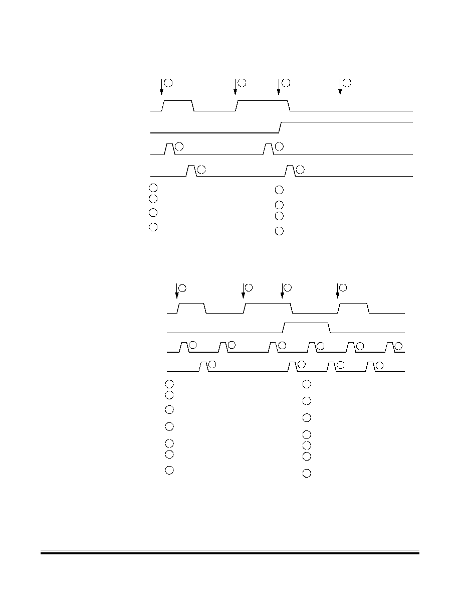
Serial Peripheral Interface (SPI) Module
Error Conditions
MC68HC908GR16 -- Rev. 1.0
Data Sheet
MOTOROLA
Serial Peripheral Interface (SPI) Module
227
Figure 16-10. Missed Read of Overflow Condition
Figure 16-11. Clearing SPRF When OVRF Interrupt Is Not Enabled
READ
READ
OVRF
SPRF
BYTE 1
BYTE 2
BYTE 3
BYTE 4
BYTE 1 SETS SPRF BIT.
CPU READS SPSCR WITH SPRF BIT SET
CPU READS BYTE 1 IN SPDR,
BYTE 2 SETS SPRF BIT.
CPU READS SPSCR WITH SPRF BIT SET
BYTE 3 SETS OVRF BIT. BYTE 3 IS LOST.
CPU READS BYTE 2 IN SPDR, CLEARING SPRF BIT,
BYTE 4 FAILS TO SET SPRF BIT BECAUSE
1
1
2
3
4
5
6
7
8
2
3
4
5
6
7
8
CLEARING SPRF BIT.
BUT NOT OVRF BIT.
OVRF BIT IS NOT CLEARED. BYTE 4 IS LOST.
AND OVRF BIT CLEAR.
AND OVRF BIT CLEAR.
SPSCR
SPDR
READ
READ
OVRF
SPRF
BYTE 1
BYTE 2
BYTE 3
BYTE 4
1
BYTE 1 SETS SPRF BIT.
CPU READS SPSCR WITH SPRF BIT SET
CPU READS BYTE 1 IN SPDR,
CPU READS SPSCR AGAIN
BYTE 2 SETS SPRF BIT.
CPU READS SPSCR WITH SPRF BIT SET
BYTE 3 SETS OVRF BIT. BYTE 3 IS LOST.
CPU READS BYTE 2 IN SPDR,
CPU READS SPSCR AGAIN
CPU READS BYTE 2 SPDR,
BYTE 4 SETS SPRF BIT.
CPU READS SPSCR.
CPU READS BYTE 4 IN SPDR,
CPU READS SPSCR AGAIN
1
2
3
CLEARING SPRF BIT.
4
TO CHECK OVRF BIT.
5
6
7
8
9
CLEARING SPRF BIT.
TO CHECK OVRF BIT.
10
CLEARING OVRF BIT.
11
12
13
14
2
3
4
5
6
7
8
9
10
11
12
13
14
CLEARING SPRF BIT.
TO CHECK OVRF BIT.
SPI RECEIVE
COMPLETE
AND OVRF BIT CLEAR.
AND OVRF BIT CLEAR.
SPSCR
SPDR

Serial Peripheral Interface (SPI) Module
Data Sheet
MC68HC908GR16 -- Rev. 1.0
228
Serial Peripheral Interface (SPI) Module
MOTOROLA
16.7.2 Mode Fault Error
Setting the SPMSTR bit selects master mode and configures the SPSCK and
MOSI pins as outputs and the MISO pin as an input. Clearing SPMSTR selects
slave mode and configures the SPSCK and MOSI pins as inputs and the MISO pin
as an output. The mode fault bit, MODF, becomes set any time the state of the
slave select pin, SS, is inconsistent with the mode selected by SPMSTR.
To prevent SPI pin contention and damage to the MCU, a mode fault error occurs if:
�
The SS pin of a slave SPI goes high during a transmission
�
The SS pin of a master SPI goes low at any time
For the MODF flag to be set, the mode fault error enable bit (MODFEN) must be
set. Clearing the MODFEN bit does not clear the MODF flag but does prevent
MODF from being set again after MODF is cleared.
MODF generates a receiver/error CPU interrupt request if the error interrupt enable
bit (ERRIE) is also set. The SPRF, MODF, and OVRF interrupts share the same
CPU interrupt vector. (See
Figure 16-12
.) It is not possible to enable MODF or
OVRF individually to generate a receiver/error CPU interrupt request. However,
leaving MODFEN low prevents MODF from being set.
In a master SPI with the mode fault enable bit (MODFEN) set, the mode fault flag
(MODF) is set if SS goes to logic 0. A mode fault in a master SPI causes the
following events to occur:
�
If ERRIE = 1, the SPI generates an SPI receiver/error CPU interrupt request.
�
The SPE bit is cleared.
�
The SPTE bit is set.
�
The SPI state counter is cleared.
�
The data direction register of the shared I/O port regains control of port
drivers.
NOTE:
To prevent bus contention with another master SPI after a mode fault error, clear
all SPI bits of the data direction register of the shared I/O port before enabling the
SPI.
When configured as a slave (SPMSTR = 0), the MODF flag is set if SS goes high
during a transmission. When CPHA = 0, a transmission begins when SS goes low
and ends once the incoming SPSCK goes back to its idle level following the shift
of the eighth data bit. When CPHA = 1, the transmission begins when the SPSCK
leaves its idle level and SS is already low. The transmission continues until the
SPSCK returns to its idle level following the shift of the last data bit. See
16.5 Transmission Formats
.
NOTE:
Setting the MODF flag does not clear the SPMSTR bit. The SPMSTR bit has no
function when SPE = 0. Reading SPMSTR when MODF = 1 shows the difference
between a MODF occurring when the SPI is a master and when it is a slave.

Serial Peripheral Interface (SPI) Module
Interrupts
MC68HC908GR16 -- Rev. 1.0
Data Sheet
MOTOROLA
Serial Peripheral Interface (SPI) Module
229
When CPHA = 0, a MODF occurs if a slave is selected (SS is at logic 0) and later
unselected (SS is at logic 1) even if no SPSCK is sent to that slave. This happens
because SS at logic 0 indicates the start of the transmission (MISO driven out with
the value of MSB) for CPHA = 0. When CPHA = 1, a slave can be selected and
then later unselected with no transmission occurring. Therefore, MODF does not
occur since a transmission was never begun.
In a slave SPI (MSTR = 0), the MODF bit generates an SPI receiver/error CPU
interrupt request if the ERRIE bit is set. The MODF bit does not clear the SPE bit
or reset the SPI in any way. Software can abort the SPI transmission by clearing
the SPE bit of the slave.
NOTE:
A logic 1 voltage on the SS pin of a slave SPI puts the MISO pin in a high
impedance state. Also, the slave SPI ignores all incoming SPSCK clocks, even if it
was already in the middle of a transmission.
To clear the MODF flag, read the SPSCR with the MODF bit set and then write to
the SPCR register. This entire clearing mechanism must occur with no MODF
condition existing or else the flag is not cleared.
16.8 Interrupts
Four SPI status flags can be enabled to generate CPU interrupt requests. See
Table 16-2
.
Reading the SPI status and control register with SPRF set and then reading the
receive data register clears SPRF. The clearing mechanism for the SPTE flag is
always just a write to the transmit data register.
The SPI transmitter interrupt enable bit (SPTIE) enables the SPTE flag to generate
transmitter CPU interrupt requests, provided that the SPI is enabled (SPE = 1).
The SPI receiver interrupt enable bit (SPRIE) enables the SPRF bit to generate
receiver CPU interrupt requests, regardless of the state of the SPE bit. See
Figure 16-12
.
The error interrupt enable bit (ERRIE) enables both the MODF and OVRF bits to
generate a receiver/error CPU interrupt request.
Table 16-2. SPI Interrupts
Flag
Request
SPTE
Transmitter empty
SPI transmitter CPU interrupt request
(SPTIE = 1, SPE = 1)
SPRF
Receiver full
SPI receiver CPU interrupt request
(SPRIE = 1)
OVRF
Overflow
SPI receiver/error interrupt request
(ERRIE = 1)
MODF
Mode fault
SPI receiver/error interrupt request
(ERRIE = 1)
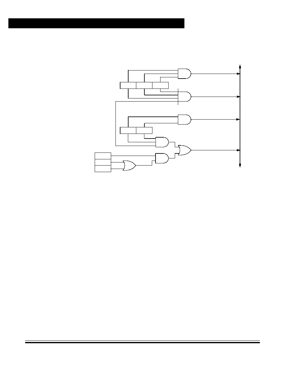
Serial Peripheral Interface (SPI) Module
Data Sheet
MC68HC908GR16 -- Rev. 1.0
230
Serial Peripheral Interface (SPI) Module
MOTOROLA
The mode fault enable bit (MODFEN) can prevent the MODF flag from being set
so that only the OVRF bit is enabled by the ERRIE bit to generate receiver/error
CPU interrupt requests.
Figure 16-12. SPI Interrupt Request Generation
The following sources in the SPI status and control register can generate CPU
interrupt requests:
�
SPI receiver full bit (SPRF) -- The SPRF bit becomes set every time a byte
transfers from the shift register to the receive data register. If the SPI
receiver interrupt enable bit, SPRIE, is also set, SPRF generates an SPI
receiver/error CPU interrupt request.
�
SPI transmitter empty (SPTE) -- The SPTE bit becomes set every time a
byte transfers from the transmit data register to the shift register. If the SPI
transmit interrupt enable bit, SPTIE, is also set, SPTE generates an SPTE
CPU interrupt request.
16.9 Resetting the SPI
Any system reset completely resets the SPI. Partial resets occur whenever the SPI
enable bit (SPE) is low. Whenever SPE is low, the following occurs:
�
The SPTE flag is set.
�
Any transmission currently in progress is aborted.
�
The shift register is cleared.
�
The SPI state counter is cleared, making it ready for a new complete
transmission.
�
All the SPI port logic is defaulted back to being general-purpose I/O.
SPTE
SPTIE
SPRF
SPRIE
SPE
CPU INTERRUPT REQUEST
CPU INTERRUPT REQUEST
NOT AVAILABLE
SPI TRANSMITTER
NOT AVAILABLE
SPI RECEIVER/ERROR
ERRIE
MODF
OVRF

Serial Peripheral Interface (SPI) Module
Low-Power Modes
MC68HC908GR16 -- Rev. 1.0
Data Sheet
MOTOROLA
Serial Peripheral Interface (SPI) Module
231
These items are reset only by a system reset:
�
All control bits in the SPCR register
�
All control bits in the SPSCR register (MODFEN, ERRIE, SPR1, and SPR0)
�
The status flags SPRF, OVRF, and MODF
By not resetting the control bits when SPE is low, the user can clear SPE between
transmissions without having to set all control bits again when SPE is set back high
for the next transmission.
By not resetting the SPRF, OVRF, and MODF flags, the user can still service these
interrupts after the SPI has been disabled. The user can disable the SPI by
writing 0 to the SPE bit. The SPI can also be disabled by a mode fault occurring in
an SPI that was configured as a master with the MODFEN bit set.
16.10 Low-Power Modes
The WAIT and STOP instructions put the MCU in low power-consumption standby
modes.
16.10.1 Wait Mode
The SPI module remains active after the execution of a WAIT instruction. In wait
mode the SPI module registers are not accessible by the CPU. Any enabled CPU
interrupt request from the SPI module can bring the MCU out of wait mode.
If SPI module functions are not required during wait mode, reduce power
consumption by disabling the SPI module before executing the WAIT instruction.
To exit wait mode when an overflow condition occurs, enable the OVRF bit to
generate CPU interrupt requests by setting the error interrupt enable bit (ERRIE).
See
16.8 Interrupts
.
16.10.2 Stop Mode
The SPI module is inactive after the execution of a STOP instruction. The STOP
instruction does not affect register conditions. SPI operation resumes after an
external interrupt. If stop mode is exited by reset, any transfer in progress is
aborted, and the SPI is reset.
16.11 SPI During Break Interrupts
The system integration module (SIM) controls whether status bits in other modules
can be cleared during the break state. The BCFE bit in the SIM break flag control
register (SBFCR) enables software to clear status bits during the break state. See
Section 15. System Integration Module (SIM).

Serial Peripheral Interface (SPI) Module
Data Sheet
MC68HC908GR16 -- Rev. 1.0
232
Serial Peripheral Interface (SPI) Module
MOTOROLA
To allow software to clear status bits during a break interrupt, write a logic 1 to the
BCFE bit. If a status bit is cleared during the break state, it remains cleared when
the MCU exits the break state.
To protect status bits during the break state, write a logic 0 to the BCFE bit. With
BCFE at logic 0 (its default state), software can read and write I/O registers during
the break state without affecting status bits. Some status bits have a 2-step
read/write clearing procedure. If software does the first step on such a bit before
the break, the bit cannot change during the break state as long as BCFE is at
logic 0. After the break, doing the second step clears the status bit.
Since the SPTE bit cannot be cleared during a break with the BCFE bit cleared, a
write to the transmit data register in break mode does not initiate a transmission nor
is this data transferred into the shift register. Therefore, a write to the SPDR in
break mode with the BCFE bit cleared has no effect.
16.12 I/O Signals
The SPI module has five I/O pins and shares four of them with a parallel I/O port.
They are:
�
MISO -- Data received
�
MOSI -- Data transmitted
�
SPSCK -- Serial clock
�
SS -- Slave select
�
CGND -- Clock ground (internally connected to V
SS
)
The SPI has limited inter-integrated circuit (I
2
C) capability (requiring software
support) as a master in a single-master environment. To communicate with I
2
C
peripherals, MOSI becomes an open-drain output when the SPWOM bit in the SPI
control register is set. In I
2
C communication, the MOSI and MISO pins are
connected to a bidirectional pin from the I
2
C peripheral and through a pullup
resistor to V
DD
.
16.12.1 MISO (Master In/Slave Out)
MISO is one of the two SPI module pins that transmits serial data. In full duplex
operation, the MISO pin of the master SPI module is connected to the MISO pin of
the slave SPI module. The master SPI simultaneously receives data on its MISO
pin and transmits data from its MOSI pin.
Slave output data on the MISO pin is enabled only when the SPI is configured as
a slave. The SPI is configured as a slave when its SPMSTR bit is logic 0 and its SS
pin is at logic 0. To support a multiple-slave system, a logic 1 on the SS pin puts
the MISO pin in a high-impedance state.
When enabled, the SPI controls data direction of the MISO pin regardless of the
state of the data direction register of the shared I/O port.

Serial Peripheral Interface (SPI) Module
I/O Signals
MC68HC908GR16 -- Rev. 1.0
Data Sheet
MOTOROLA
Serial Peripheral Interface (SPI) Module
233
16.12.2 MOSI (Master Out/Slave In)
MOSI is one of the two SPI module pins that transmits serial data. In full-duplex
operation, the MOSI pin of the master SPI module is connected to the MOSI pin of
the slave SPI module. The master SPI simultaneously transmits data from its MOSI
pin and receives data on its MISO pin.
When enabled, the SPI controls data direction of the MOSI pin regardless of the
state of the data direction register of the shared I/O port.
16.12.3 SPSCK (Serial Clock)
The serial clock synchronizes data transmission between master and slave
devices. In a master MCU, the SPSCK pin is the clock output. In a slave MCU, the
SPSCK pin is the clock input. In full-duplex operation, the master and slave MCUs
exchange a byte of data in eight serial clock cycles.
When enabled, the SPI controls data direction of the SPSCK pin regardless of the
state of the data direction register of the shared I/O port.
16.12.4 SS (Slave Select)
The SS pin has various functions depending on the current state of the SPI. For an
SPI configured as a slave, the SS is used to select a slave. For CPHA = 0, the SS
is used to define the start of a transmission. (See
16.5 Transmission Formats
.)
Since it is used to indicate the start of a transmission, the SS must be toggled high
and low between each byte transmitted for the CPHA = 0 format. However, it can
remain low between transmissions for the CPHA = 1 format. See
Figure 16-13
.
Figure 16-13. CPHA/SS Timing
When an SPI is configured as a slave, the SS pin is always configured as an input.
It cannot be used as a general-purpose I/O regardless of the state of the MODFEN
control bit. However, the MODFEN bit can still prevent the state of the SS from
creating a MODF error. See
16.13.2 SPI Status and Control Register.
NOTE:
A logic 1 voltage on the SS pin of a slave SPI puts the MISO pin in a
high-impedance state. The slave SPI ignores all incoming SPSCK clocks, even if
it was already in the middle of a transmission.
When an SPI is configured as a master, the SS input can be used in conjunction
with the MODF flag to prevent multiple masters from driving MOSI and SPSCK.
BYTE 1
BYTE 3
MISO/MOSI
BYTE 2
MASTER SS
SLAVE SS
CPHA = 0
SLAVE SS
CPHA = 1
Serial Peripheral Interface (SPI) Module
Data Sheet
MC68HC908GR16 -- Rev. 1.0
234
Serial Peripheral Interface (SPI) Module
MOTOROLA
(See
16.7.2 Mode Fault Error.)
For the state of the SS pin to set the MODF flag,
the MODFEN bit in the SPSCK register must be set. If the MODFEN bit is low for
an SPI master, the SS pin can be used as a general-purpose I/O under the control
of the data direction register of the shared I/O port. With MODFEN high, it is an
input-only pin to the SPI regardless of the state of the data direction register of the
shared I/O port.
The CPU can always read the state of the SS pin by configuring the appropriate
pin as an input and reading the port data register. See
Table 16-3
.
16.12.5 CGND (Clock Ground)
CGND is the ground return for the serial clock pin, SPSCK, and the ground for the
port output buffers. It is internally connected to V
SS
as shown in
Table 16-1
.
16.13 I/O Registers
Three registers control and monitor SPI operation:
�
SPI control register (SPCR)
�
SPI status and control register (SPSCR)
�
SPI data register (SPDR)
16.13.1 SPI Control Register
The SPI control register:
�
Enables SPI module interrupt requests
�
Configures the SPI module as master or slave
�
Selects serial clock polarity and phase
�
Configures the SPSCK, MOSI, and MISO pins as open-drain outputs
�
Enables the SPI module
Table 16-3. SPI Configuration
SPE
SPMSTR
MODFEN
SPI Configuration
State of SS Logic
0
X
(1))
1. X = Don't care
X
Not enabled
General-purpose I/O; SS ignored by SPI
1
0
X
Slave
Input-only to SPI
1
1
0
Master without MODF
General-purpose I/O; SS ignored by SPI
1
1
1
Master with MODF
Input-only to SPI

Serial Peripheral Interface (SPI) Module
I/O Registers
MC68HC908GR16 -- Rev. 1.0
Data Sheet
MOTOROLA
Serial Peripheral Interface (SPI) Module
235
SPRIE -- SPI Receiver Interrupt Enable Bit
This read/write bit enables CPU interrupt requests generated by the SPRF bit.
The SPRF bit is set when a byte transfers from the shift register to the receive
data register. Reset clears the SPRIE bit.
1 = SPRF CPU interrupt requests enabled
0 = SPRF CPU interrupt requests disabled
SPMSTR -- SPI Master Bit
This read/write bit selects master mode operation or slave mode operation.
Reset sets the SPMSTR bit.
1 = Master mode
0 = Slave mode
CPOL -- Clock Polarity Bit
This read/write bit determines the logic state of the SPSCK pin between
transmissions. (See
Figure 16-5
and
Figure 16-7
.) To transmit data between
SPI modules, the SPI modules must have identical CPOL values. Reset clears
the CPOL bit.
CPHA -- Clock Phase Bit
This read/write bit controls the timing relationship between the serial clock and
SPI data. (See
Figure 16-5
and
Figure 16-7
.) To transmit data between SPI
modules, the SPI modules must have identical CPHA values. When CPHA = 0,
the SS pin of the slave SPI module must be set to logic 1 between bytes. (See
Figure 16-13
.) Reset sets the CPHA bit.
SPWOM -- SPI Wired-OR Mode Bit
This read/write bit disables the pullup devices on pins SPSCK, MOSI, and MISO
so that those pins become open-drain outputs.
1 = Wired-OR SPSCK, MOSI, and MISO pins
0 = Normal push-pull SPSCK, MOSI, and MISO pins
SPE -- SPI Enable
This read/write bit enables the SPI module. Clearing SPE causes a partial reset
of the SPI. (See
16.9 Resetting the SPI
.) Reset clears the SPE bit.
1 = SPI module enabled
0 = SPI module disabled
Address: $0010
Bit 7
6
5
4
3
2
1
Bit 0
Read:
SPRIE
R
SPMSTR
CPOL
CPHA
SPWOM
SPE
SPTIE
Write:
Reset:
0
0
1
0
1
0
0
0
R
= Reserved
= Unimplemented
Figure 16-14. SPI Control Register (SPCR)

Serial Peripheral Interface (SPI) Module
Data Sheet
MC68HC908GR16 -- Rev. 1.0
236
Serial Peripheral Interface (SPI) Module
MOTOROLA
SPTIE-- SPI Transmit Interrupt Enable
This read/write bit enables CPU interrupt requests generated by the SPTE bit.
SPTE is set when a byte transfers from the transmit data register to the shift
register. Reset clears the SPTIE bit.
1 = SPTE CPU interrupt requests enabled
0 = SPTE CPU interrupt requests disabled
16.13.2 SPI Status and Control Register
The SPI status and control register contains flags to signal these conditions:
�
Receive data register full
�
Failure to clear SPRF bit before next byte is received (overflow error)
�
Inconsistent logic level on SS pin (mode fault error)
�
Transmit data register empty
The SPI status and control register also contains bits that perform these functions:
�
Enable error interrupts
�
Enable mode fault error detection
�
Select master SPI baud rate
SPRF -- SPI Receiver Full Bit
This clearable, read-only flag is set each time a byte transfers from the shift
register to the receive data register. SPRF generates a CPU interrupt request if
the SPRIE bit in the SPI control register is set also.
During an SPRF CPU interrupt, the CPU clears SPRF by reading the SPI status
and control register with SPRF set and then reading the SPI data register.
Reset clears the SPRF bit.
1 = Receive data register full
0 = Receive data register not full
ERRIE -- Error Interrupt Enable Bit
This read/write bit enables the MODF and OVRF bits to generate CPU interrupt
requests. Reset clears the ERRIE bit.
1 = MODF and OVRF can generate CPU interrupt requests
0 = MODF and OVRF cannot generate CPU interrupt requests
Address: $0011
Bit 7
6
5
4
3
2
1
Bit 0
Read:
SPRF
ERRIE
OVRF
MODF
SPTE
MODFEN
SPR1
SPR0
Write:
Reset:
0
0
0
0
1
0
0
0
= Unimplemented
Figure 16-15. SPI Status and Control Register (SPSCR)

Serial Peripheral Interface (SPI) Module
I/O Registers
MC68HC908GR16 -- Rev. 1.0
Data Sheet
MOTOROLA
Serial Peripheral Interface (SPI) Module
237
OVRF -- Overflow Bit
This clearable, read-only flag is set if software does not read the byte in the
receive data register before the next full byte enters the shift register. In an
overflow condition, the byte already in the receive data register is unaffected,
and the byte that shifted in last is lost. Clear the OVRF bit by reading the SPI
status and control register with OVRF set and then reading the receive data
register. Reset clears the OVRF bit.
1 = Overflow
0 = No overflow
MODF -- Mode Fault Bit
This clearable, read-only flag is set in a slave SPI if the SS pin goes high during
a transmission with the MODFEN bit set. In a master SPI, the MODF flag is set
if the SS pin goes low at any time with the MODFEN bit set. Clear the MODF bit
by reading the SPI status and control register (SPSCR) with MODF set and then
writing to the SPI control register (SPCR). Reset clears the MODF bit.
1 = SS pin at inappropriate logic level
0 = SS pin at appropriate logic level
SPTE -- SPI Transmitter Empty Bit
This clearable, read-only flag is set each time the transmit data register
transfers a byte into the shift register. SPTE generates an SPTE CPU interrupt
request or an SPTE DMA service request if the SPTIE bit in the SPI control
register is set also.
NOTE:
Do not write to the SPI data register unless the SPTE bit is high.
During an SPTE CPU interrupt, the CPU clears the SPTE bit by writing to the
transmit data register.
Reset sets the SPTE bit.
1 = Transmit data register empty
0 = Transmit data register not empty
MODFEN -- Mode Fault Enable Bit
This read/write bit, when set to 1, allows the MODF flag to be set. If the MODF
flag is set, clearing the MODFEN does not clear the MODF flag. If the SPI is
enabled as a master and the MODFEN bit is low, then the SS pin is available as
a general-purpose I/O.
If the MODFEN bit is set, then this pin is not available as a general-purpose I/O.
When the SPI is enabled as a slave, the SS pin is not available as a
general-purpose I/O regardless of the value of MODFEN. See
16.12.4 SS
(Slave Select).
If the MODFEN bit is low, the level of the SS pin does not affect the operation
of an enabled SPI configured as a master. For an enabled SPI configured as a
slave, having MODFEN low only prevents the MODF flag from being set. It does
not affect any other part of SPI operation. See
16.7.2 Mode Fault Error.

Serial Peripheral Interface (SPI) Module
Data Sheet
MC68HC908GR16 -- Rev. 1.0
238
Serial Peripheral Interface (SPI) Module
MOTOROLA
SPR1 and SPR0 -- SPI Baud Rate Select Bits
In master mode, these read/write bits select one of four baud rates as shown in
Table 16-4
. SPR1 and SPR0 have no effect in slave mode. Reset clears SPR1
and SPR0.
Use this formula to calculate the SPI baud rate:
where:
CGMOUT = base clock output of the clock generator module (CGM)
BD = baud rate divisor
16.13.3 SPI Data Register
The SPI data register consists of the read-only receive data register and the
write-only transmit data register. Writing to the SPI data register writes data into the
transmit data register. Reading the SPI data register reads data from the receive
data register. The transmit data and receive data registers are separate registers
that can contain different values. See
Figure 16-3
.
R7�R0/T7�T0 -- Receive/Transmit Data Bits
NOTE:
Do not use read-modify-write instructions on the SPI data register since the register
read is not the same as the register written.
Table 16-4. SPI Master Baud Rate Selection
SPR1 and SPR0
Baud Rate Divisor (BD)
00
2
01
8
10
32
11
128
Baud rate
CGMOUT
2
BD
�
--------------------------
=
Address: $0012
Bit 7
6
5
4
3
2
1
Bit 0
Read:
R7
R6
R5
R4
R3
R2
R1
R0
Write:
T7
T6
T5
T4
T3
T2
T1
T0
Reset:
Unaffected by reset
Figure 16-16. SPI Data Register (SPDR)

MC68HC908GR16 -- Rev. 1.0
Data Sheet
MOTOROLA
Timebase Module (TBM)
239
Data Sheet -- MC68HC908GR16
Section 17. Timebase Module (TBM)
17.1 Introduction
This section describes the timebase module (TBM). The TBM will generate
periodic interrupts at user selectable rates using a counter clocked by the external
clock source. This TBM version uses 15 divider stages, eight of which are user
selectable. A configuration option bit to select an additional 128 divide of the
external clock source can be selected. See
Section 5. Configuration Register
(CONFIG)
17.2 Features
Features of the TBM module include:
�
External clock or an additional divide-by-128 selected by configuration
option bit as clock source
�
Software configurable periodic interrupts with divide-by: 8, 16, 32, 64, 128,
2048, 8192, and 32768 taps of the selected clock source
�
Configurable for operation during stop mode to allow periodic wakeup from
stop
17.3 Functional Description
This module can generate a periodic interrupt by dividing the clock source supplied
from the clock generator module, CGMXCLK.
The counter is initialized to all 0s when TBON bit is cleared. The counter, shown in
Figure 17-1
, starts counting when the TBON bit is set. When the counter overflows
at the tap selected by TBR2�TBR0, the TBIF bit gets set. If the TBIE bit is set, an
interrupt request is sent to the CPU. The TBIF flag is cleared by writing a 1 to the
TACK bit. The first time the TBIF flag is set after enabling the timebase module, the
interrupt is generated at approximately half of the overflow period. Subsequent
events occur at the exact period.
The timebase module may remain active after execution of the STOP instruction if
the crystal oscillator has been enabled to operate during stop mode through the
OSCENINSTOP bit in the configuration register. The timebase module can be
used in this mode to generate a periodic wakeup from stop mode.
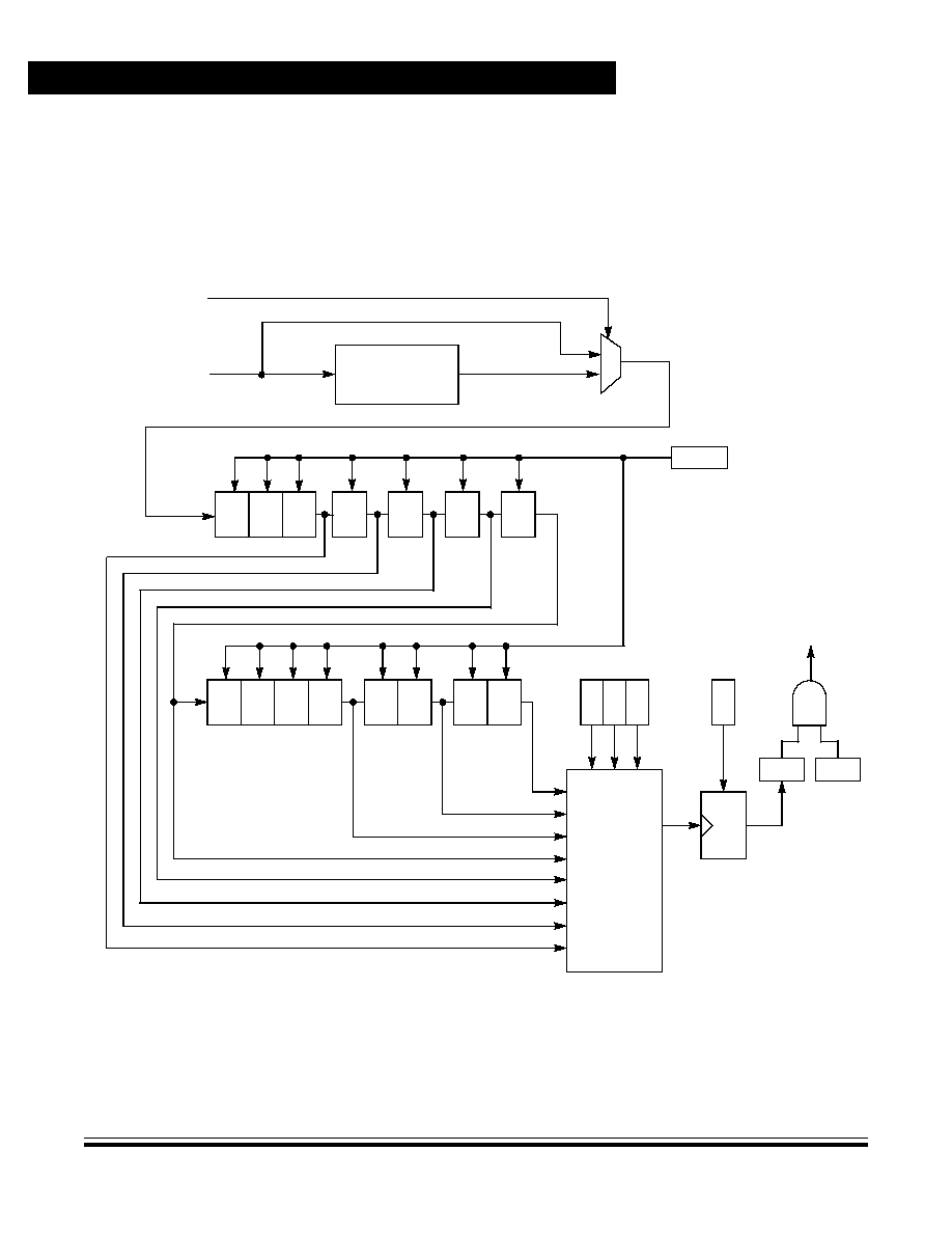
Timebase Module (TBM)
Data Sheet
MC68HC908GR16 -- Rev. 1.0
240
Timebase Module (TBM)
MOTOROLA
17.4 Interrupts
The timebase module can periodically interrupt the CPU with a rate defined by the
selected TBMCLK and the select bits TBR2�TBR0. When the timebase counter
chain rolls over, the TBIF flag is set. If the TBIE bit is set, enabling the timebase
interrupt, the counter chain overflow will generate a CPU interrupt request.
Figure 17-1. Timebase Block Diagram
NOTE:
Interrupts must be acknowledged by writing a logic 1 to the TACK bit.
� 2
� 2
� 2
� 2
� 2
� 2
� 2
� 2
� 2
� 2
� 2
� 2
� 2
� 2
SEL
0 0 0
0 0 1
0 1 0
0 1 1
TBIF
TBR1
TBR0
TBIE
TBMINT
TBON
� 2
R
T
ACK
TBR2
1 0 0
1 0 1
1 1 0
1 1 1
TBMCLK
FROM CGM MODULE
TBMCLKSEL
FROM CONFIG2
DIVIDE BY 128
PRESCALER
0
1
CGMXCLK

Timebase Module (TBM)
TBM Interrupt Rate
MC68HC908GR16 -- Rev. 1.0
Data Sheet
MOTOROLA
Timebase Module (TBM)
241
17.5 TBM Interrupt Rate
The interrupt rate is determined by the equation:
where:
f
TBMCLK
= Frequency supplied from the clock generator (CGM) module
Divider = Divider value as determined by TBR2�TBR0 settings,
see
Table 17-1
As an example, a clock source of 4.9152 MHz, with the TMCLKSEL set for
divide-by-128 and the TBR2�TBR0 set to {011}, the divider tap is1 and the interrupt
rate calculates to:
1/(4.9152 x 10
6
/128)
= 26
�
s
NOTE:
Do not change TBR2�TBR0 bits while the timebase is enabled (TBON = 1).
17.6 Low-Power Modes
The WAIT and STOP instructions put the MCU in low power- consumption standby
modes.
17.6.1 Wait Mode
The timebase module remains active after execution of the WAIT instruction. In
wait mode the timebase register is not accessible by the CPU.
If the timebase functions are not required during wait mode, reduce the power
consumption by stopping the timebase before executing the WAIT instruction.
Table 17-1. Timebase Divider Selection
TBR2
TBR1
TBR0
Divider Tap
TMBCLKSEL
0
1
0
0
0
32,768
4,194,304
0
0
1
8192
1,048,576
0
1
0
2048
262144
0
1
1
128
16,384
1
0
0
64
8192
1
0
1
32
4096
1
1
0
16
2048
1
1
1
8
1024
t
TBMRATE
1
f
TBMRATE
--------------------------------
Divider
f
TBMCLK
----------------------------
=
=
Timebase Module (TBM)
Data Sheet
MC68HC908GR16 -- Rev. 1.0
242
Timebase Module (TBM)
MOTOROLA
17.6.2 Stop Mode
The timebase module may remain active after execution of the STOP instruction if
the internal clock generator has been enabled to operate during stop mode through
the OSCENINSTOP bit in the configuration register. The timebase module can be
used in this mode to generate a periodic wakeup from stop mode.
If the internal clock generator has not been enabled to operate in stop mode, the
timebase module will not be active during stop mode. In stop mode, the timebase
register is not accessible by the CPU.
If the timebase functions are not required during stop mode, reduce power
consumption by disabling the timebase module before executing the STOP
instruction.
17.7 Timebase Control Register
The timebase has one register, the timebase control register (TBCR), which is
used to enable the timebase interrupts and set the rate.
TBIF -- Timebase Interrupt Flag
This read-only flag bit is set when the timebase counter has rolled over.
1 = Timebase interrupt pending
0 = Timebase interrupt not pending
TBR2�TBR0 -- Timebase Divider Selection Bits
These read/write bits select the tap in the counter to be used for timebase
interrupts as shown in
Table 17-1
.
NOTE:
Do not change TBR2�TBR0 bits while the timebase is enabled
(TBON = 1).
TACK-- Timebase Acknowledge Bit
The TACK bit is a write-only bit and always reads as 0. Writing a logic 1 to this
bit clears TBIF, the timebase interrupt flag bit. Writing a logic 0 to this bit has no
effect.
1 = Clear timebase interrupt flag
0 = No effect
Address: $001C
Bit 7
6
5
4
3
2
1
Bit 0
Read:
TBIF
TBR2
TBR1
TBR0
0
TBIE
TBON
R
Write:
TACK
Reset:
0
0
0
0
0
0
0
0
= Unimplemented
R
= Reserved
Figure 17-2. Timebase Control Register (TBCR)

Timebase Module (TBM)
Timebase Control Register
MC68HC908GR16 -- Rev. 1.0
Data Sheet
MOTOROLA
Timebase Module (TBM)
243
TBIE -- Timebase Interrupt Enabled Bit
This read/write bit enables the timebase interrupt when the TBIF bit becomes
set. Reset clears the TBIE bit.
1 = Timebase interrupt is enabled.
0 = Timebase interrupt is disabled.
TBON -- Timebase Enabled Bit
This read/write bit enables the timebase. Timebase may be turned off to reduce
power consumption when its function is not necessary. The counter can be
initialized by clearing and then setting this bit. Reset clears the TBON bit.
1 = Timebase is enabled.
0 = Timebase is disabled and the counter initialized to 0s.

Timebase Module (TBM)
Data Sheet
MC68HC908GR16 -- Rev. 1.0
244
Timebase Module (TBM)
MOTOROLA
MC68HC908GR16 -- Rev. 1.0
Data Sheet
MOTOROLA
Timer Interface Module (TIM)
245
Data Sheet -- MC68HC908GR16
Section 18. Timer Interface Module (TIM)
18.1 Introduction
This section describes the timer interface (TIM) module. The TIM is a two-channel
timer that provides a timing reference with input capture, output compare, and
pulse-width-modulation functions.
Figure 18-1
is a block diagram of the TIM.
This particular MCU has two timer interface modules which are denoted as TIM1
and TIM2.
Figure 18-1. TIM Block Diagram
PRESCALER
PRESCALER SELECT
INTERNAL
16-BIT COMPARATOR
PS2
PS1
PS0
16-BIT COMPARATOR
16-BIT LATCH
TCH0H:TCH0L
MS0A
ELS0B
ELS0A
TOF
TOIE
16-BIT COMPARATOR
16-BIT LATCH
TCH1H:TCH1L
CHANNEL 0
CHANNEL 1
TMODH:TMODL
TRST
TSTOP
TOV0
CH0IE
CH0F
ELS1B
ELS1A
TOV1
CH1IE
CH1MAX
CH1F
CH0MAX
MS0B
16-BIT COUNTER
INTERNAL
BUS
BUS CLOCK
MS1A
T[1,2]CH0
T[1,2]CH1
INTERRUPT
LOGIC
PORT
LOGIC
INTERRUPT
LOGIC
INTERRUPT
LOGIC
PORT
LOGIC
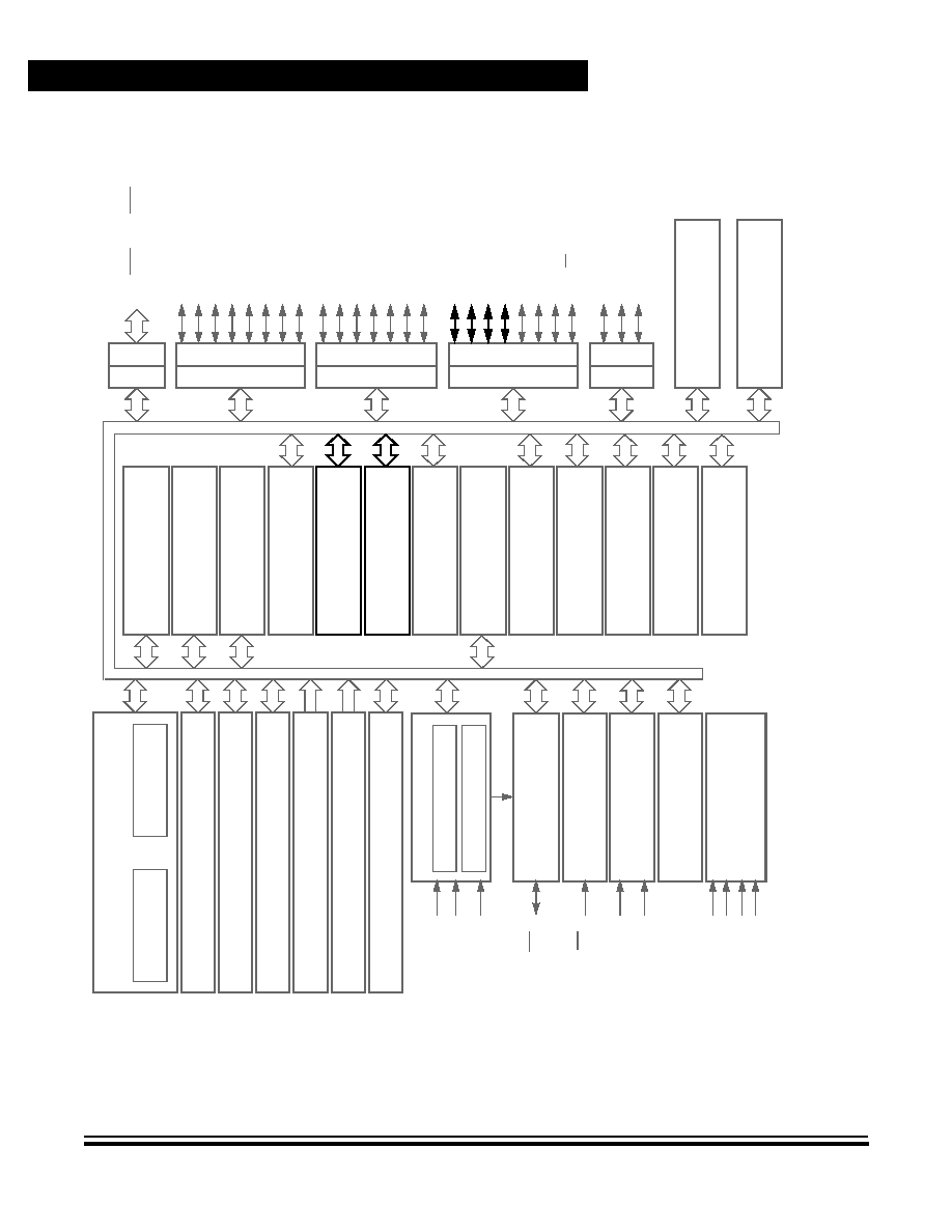
Data Sheet
MC6
8
HC90
8
GR16 --
Re
v. 1.0
246
Timer Inter
f
ace
Module (TIM)
M
OTOROLA
Timer Interface Module (TIM)
Figure 18-2. Block Diagram Highlighting TIM Blocks and Pins
MONITOR MODULE
M68HC08 CPU
CONTROL AND STATUS REGISTERS -- 64 BYTES
USER FLASH -- 15,872 BYTES
USER RAM -- 1024 BYTES
MONITOR ROM -- 350 BYTES
USER FLASH VECTOR SPACE -- 44 BYTES
PORTA
D
DRA
DDRC
PO
R
T
C
DDR
D
PORTD
DDRE
POR
T
E
INTERNAL BUS
OSC1
OSC2
RST
(3)
IRQ
(3)
PTA7/KBD7�PTA0/KBD0
(1)
PTB7/AD7
PTB6/AD6
PTB5/AD5
PTB4/AD4
PTB3/AD3
PTB2/AD2
PTB1/AD1
PTB0/AD0
PTC6
(1)
PTC5
(1)
PTC4
(1), (2)
PTC3
(1), (2)
PTC2
(1), (2)
PTC1
(1), (2)
PTC0
(1), (2)
PTD7/T2CH1
(1)
PTD6/T2CH0
(1)
PTD5/T1CH1
(1)
PTD4/T1CH0
(1)
PTD3/SPSCK
(1)
PTD2/MOSI
(1)
PTD1/MISO
(1)
PTD0/SS
(1)
PTE1/RxD
PTE0/TxD
SECURITY
MODULE
POWER
V
SS
V
DD
V
SSA
V
DDA
1. Ports are software configurable with pullup device if input port.
2. Higher current drive port pins
3. Pin contains integrated pullup device
MONITOR MODE ENTRY
MODULE
DDRB
PORTB
V
DDAD
/V
REFH
V
DDAD
/V
REFL
PTE5�PTE2
FLASH PROGRAMMING ROUTINES ROM -- 406 BYTES
CLOCK GENERATOR MODULE
CGMXFC
PHASE LOCKED LOOP
32�100 kHz OSCILLATOR
CPU
REGISTERS
ARITHMETIC/LOGIC
UNIT (ALU)
SYSTEM INTEGRATION
MODULE
SINGLE EXTERNAL
INTERRUPT MODULE
10-BIT ANALOG-TO-DIGITAL
CONVERTER MODULE
POWER-ON RESET
MODULE
PROGRAMMABLE TIMEBASE
MODULE
SINGLE BREAKPOINT
BREAK MODULE
DUAL VOLTAGE
LOW-VOLTAGE INHIBIT
MODULE
8-BIT KEYBOARD
INTERRUPT MODULE
2-CHANNEL TIMER
INTERFACE MODULE 1
2-CHANNEL TIMER
INTERFACE MODULE 2
ENHANCED SERIAL
COMUNICATIONS
INTERFACE MODULE
COMPUTER OPERATING
PROPERLY MODULE
SERIAL PERIPHERAL
INTERFACE MODULE
DATA BUS SWITCH
MODULE
MEMORY MAP
MODULE
CONFIGURATION
REGISTER 1�2
MODULE

Timer Interface Module (TIM)
Features
MC68HC908GR16 -- Rev. 1.0
Data Sheet
MOTOROLA
Timer Interface Module (TIM)
247
18.2 Features
Features of the TIM include:
�
Two input capture/output compare channels:
�
Rising-edge, falling-edge, or any-edge input capture trigger
�
Set, clear, or toggle output compare action
�
Buffered and unbuffered pulse-width-modulation (PWM) signal generation
�
Programmable TIM clock input with 7-frequency internal bus clock prescaler
selection
�
Free-running or modulo up-count operation
�
Toggle any channel pin on overflow
�
TIM counter stop and reset bits
18.3 Pin Name Conventions
The text that follows describes both timers, TIM1 and TIM2. The TIM input/output
(I/O) pin names are T[1,2]CH0 (timer channel 0) and T[1,2]CH1 (timer channel 1),
where "1" is used to indicate TIM1 and "2" is used to indicate TIM2. The two TIMs
share four I/O pins with four port D I/O port pins. The full names of the TIM I/O pins
are listed in
Table 18-1
.
The generic pin names appear in the text that follows.
NOTE:
References to either timer 1 or timer 2 may be made in the following text by omitting
the timer number. For example, TCH0 may refer generically to T1CH0 and T2CH0,
and TCH1 may refer to T1CH1 and T2CH1.
18.4 Functional Description
Figure 18-1
shows the structure of the TIM. The central component of the TIM is
the 16-bit TIM counter that can operate as a free-running counter or a modulo
up-counter. The TIM counter provides the timing reference for the input capture
and output compare functions. The TIM counter modulo registers,
TMODH:TMODL, control the modulo value of the TIM counter. Software can read
the TIM counter value at any time without affecting the counting sequence.
The two TIM channels (per timer) are programmable independently as input
capture or output compare channels. If a channel is configured as input capture,
Table 18-1. Pin Name Conventions
TIM Generic Pin Names:
T[1,2]CH0
T[1,2]CH1
Full TIM Pin Names:
TIM1
PTD4/T1CH0
PTD5/T1CH1
TIM2
PTD6/T2CH0
PTD7/T2CH1
Timer Interface Module (TIM)
Data Sheet
MC68HC908GR16 -- Rev. 1.0
248
Timer Interface Module (TIM)
MOTOROLA
then an internal pullup device may be enabled for that channel. See
12.5.3 Port D
Input Pullup Enable Register.
Figure 18-3
summarizes the timer registers.
NOTE:
References to either timer 1 or timer 2 may be made in the following text by omitting
the timer number. For example, TSC may generically refer to both T1SC and
T2SC.
Addr.
Register Name
Bit 7
6
5
4
3
2
1
Bit 0
$0020
Timer 1 Status and Control
Register (T1SC)
See page 256.
Read:
TOF
TOIE
TSTOP
0
0
PS2
PS1
PS0
Write:
0
TRST
Reset:
0
0
1
0
0
0
0
0
$0021
Timer 1 Counter
Register High (T1CNTH)
See page 258.
Read:
Bit 15
14
13
12
11
10
9
Bit 8
Write:
Reset:
0
0
0
0
0
0
0
0
$0022
Timer 1 Counter
Register Low (T1CNTL)
See page 258.
Read:
Bit 7
6
5
4
3
2
1
Bit 0
Write:
Reset:
0
0
0
0
0
0
0
0
$0023
Timer 1 Counter Modulo
Register High (T1MODH)
See page 258.
Read:
Bit 15
14
13
12
11
10
9
Bit 8
Write:
Reset:
1
1
1
1
1
1
1
1
$0024
Timer 1 Counter Modulo
Register Low (T1MODL)
See page 259.
Read:
Bit 7
6
5
4
3
2
1
Bit 0
Write:
Reset:
1
1
1
1
1
1
1
1
$0025
Timer 1 Channel 0 Status and
Control Register (T1SC0)
See page 259.
Read:
CH0F
CH0IE
MS0B
MS0A
ELS0B
ELS0A
TOV0
CH0MAX
Write:
0
Reset:
0
0
0
0
0
0
0
0
$0026
Timer 1 Channel 0
Register High (T1CH0H)
See page 262.
Read:
Bit 15
14
13
12
11
10
9
Bit 8
Write:
Reset:
Indeterminate after reset
$0027
Timer 1 Channel 0
Register Low (T1CH0L)
See page 262.
Read:
Bit 7
6
5
4
3
2
1
Bit 0
Write:
Reset:
Indeterminate after reset
$0028
Timer 1 Channel 1 Status and
Control Register (T1SC1)
See page 259.
Read:
CH1F
CH1IE
0
MS1A
ELS1B
ELS1A
TOV1
CH1MAX
Write:
0
Reset:
0
0
0
0
0
0
0
0
$0029
Timer 1 Channel 1
Register High (T1CH1H)
See page 262.
Read:
Bit 15
14
13
12
11
10
9
Bit 8
Write:
Reset:
Indeterminate after reset
= Unimplemented
Figure 18-3. TIM I/O Register Summary (Sheet 1 of 2)
Timer Interface Module (TIM)
Functional Description
MC68HC908GR16 -- Rev. 1.0
Data Sheet
MOTOROLA
Timer Interface Module (TIM)
249
$002A
Timer 1 Channel 1
Register Low (T1CH1L)
See page 262.
Read:
Bit 7
6
5
4
3
2
1
Bit 0
Write:
Reset:
Indeterminate after reset
$002B
Timer 2 Status and Control
Register (T2SC)
See page 256.
Read:
TOF
TOIE
TSTOP
0
0
PS2
PS1
PS0
Write:
0
TRST
Reset:
0
0
1
0
0
0
0
0
$002C
Timer 2 Counter
Register High (T2CNTH)
See page 258.
Read:
Bit 15
14
13
12
11
10
9
Bit 8
Write:
Reset:
0
0
0
0
0
0
0
0
$002D
Timer 2 Counter
Register Low (T2CNTL)
See page 258.
Read:
Bit 7
6
5
4
3
2
1
Bit 0
Write:
Reset:
0
0
0
0
0
0
0
0
$002E
Timer 2 Counter Modulo
Register High (T2MODH)
See page 258.
Read:
Bit 15
14
13
12
11
10
9
Bit 8
Write:
Reset:
1
1
1
1
1
1
1
1
$002F
Timer 2 Counter Modulo
Register Low (T2MODL)
See page 259.
Read:
Bit 7
6
5
4
3
2
1
Bit 0
Write:
Reset:
1
1
1
1
1
1
1
1
$0030
Timer 2 Channel 0 Status and
Control Register (T2SC0)
See page 259.
Read:
CH0F
CH0IE
MS0B
MS0A
ELS0B
ELS0A
TOV0
CH0MAX
Write:
0
Reset:
0
0
0
0
0
0
0
0
$0031
Timer 2 Channel 0
Register High (T2CH0H)
See page 262.
Read:
Bit 15
14
13
12
11
10
9
Bit 8
Write:
Reset:
Indeterminate after reset
$0032
Timer 2 Channel 0
Register Low (T2CH0L)
See page 262.
Read:
Bit 7
6
5
4
3
2
1
Bit 0
Write:
Reset:
Indeterminate after reset
$0033
Timer 2 Channel 1 Status and
Control Register (T2SC1)
See page 259.
Read:
CH1F
CH1IE
0
MS1A
ELS1B
ELS1A
TOV1
CH1MAX
Write:
0
Reset:
0
0
0
0
0
0
0
0
$0034
Timer 2 Channel 1
Register High (T2CH1H)
See page 262.
Read:
Bit 15
14
13
12
11
10
9
Bit 8
Write:
Reset:
Indeterminate after reset
$0035
Timer 2 Channel 1
Register Low (T2CH1L)
See page 262.
Read:
Bit 7
6
5
4
3
2
1
Bit 0
Write:
Reset:
Indeterminate after reset
Addr.
Register Name
Bit 7
6
5
4
3
2
1
Bit 0
= Unimplemented
Figure 18-3. TIM I/O Register Summary (Sheet 2 of 2)

Timer Interface Module (TIM)
Data Sheet
MC68HC908GR16 -- Rev. 1.0
250
Timer Interface Module (TIM)
MOTOROLA
18.4.1 TIM Counter Prescaler
The TIM clock source can be one of the seven prescaler outputs. The prescaler
generates seven clock rates from the internal bus clock. The prescaler select bits,
PS[2:0], in the TIM status and control register select the TIM clock source.
18.4.2 Input Capture
With the input capture function, the TIM can capture the time at which an external
event occurs. When an active edge occurs on the pin of an input capture channel,
the TIM latches the contents of the TIM counter into the TIM channel registers,
TCHxH:TCHxL. The polarity of the active edge is programmable. Input captures
can generate TIM CPU interrupt requests.
18.4.3 Output Compare
With the output compare function, the TIM can generate a periodic pulse with a
programmable polarity, duration, and frequency. When the counter reaches the
value in the registers of an output compare channel, the TIM can set, clear, or
toggle the channel pin. Output compares can generate TIM CPU interrupt
requests.
18.4.3.1 Unbuffered Output Compare
Any output compare channel can generate unbuffered output compare pulses as
described in
18.4.3 Output Compare
. The pulses are unbuffered because
changing the output compare value requires writing the new value over the old
value currently in the TIM channel registers.
An unsynchronized write to the TIM channel registers to change an output compare
value could cause incorrect operation for up to two counter overflow periods. For
example, writing a new value before the counter reaches the old value but after the
counter reaches the new value prevents any compare during that counter overflow
period. Also, using a TIM overflow interrupt routine to write a new, smaller output
compare value may cause the compare to be missed. The TIM may pass the new
value before it is written.
Use the following methods to synchronize unbuffered changes in the output
compare value on channel x:
�
When changing to a smaller value, enable channel x output compare
interrupts and write the new value in the output compare interrupt routine.
The output compare interrupt occurs at the end of the current output
compare pulse. The interrupt routine has until the end of the counter
overflow period to write the new value.
�
When changing to a larger output compare value, enable TIM overflow
interrupts and write the new value in the TIM overflow interrupt routine. The
TIM overflow interrupt occurs at the end of the current counter overflow

Timer Interface Module (TIM)
Functional Description
MC68HC908GR16 -- Rev. 1.0
Data Sheet
MOTOROLA
Timer Interface Module (TIM)
251
period. Writing a larger value in an output compare interrupt routine (at the
end of the current pulse) could cause two output compares to occur in the
same counter overflow period.
18.4.3.2 Buffered Output Compare
Channels 0 and 1 can be linked to form a buffered output compare channel whose
output appears on the TCH0 pin. The TIM channel registers of the linked pair
alternately control the output.
Setting the MS0B bit in TIM channel 0 status and control register (TSC0) links
channel 0 and channel 1. The output compare value in the TIM channel 0 registers
initially controls the output on the TCH0 pin. Writing to the TIM channel 1 registers
enables the TIM channel 1 registers to synchronously control the output after the
TIM overflows. At each subsequent overflow, the TIM channel registers (0 or 1) that
control the output are the ones written to last. TSC0 controls and monitors the
buffered output compare function, and TIM channel 1 status and control register
(TSC1) is unused. While the MS0B bit is set, the channel 1 pin, TCH1, is available
as a general-purpose I/O pin.
NOTE:
In buffered output compare operation, do not write new output compare values to
the currently active channel registers. User software should track the currently
active channel to prevent writing a new value to the active channel. Writing to the
active channel registers is the same as generating unbuffered output compares.
18.4.4 Pulse Width Modulation (PWM)
By using the toggle-on-overflow feature with an output compare channel, the TIM
can generate a PWM signal. The value in the TIM counter modulo registers
determines the period of the PWM signal. The channel pin toggles when the
counter reaches the value in the TIM counter modulo registers. The time between
overflows is the period of the PWM signal.
As
Figure 18-4
shows, the output compare value in the TIM channel registers
determines the pulse width of the PWM signal. The time between overflow and
output compare is the pulse width. Program the TIM to clear the channel pin on
output compare if the state of the PWM pulse is logic 1. Program the TIM to set the
pin if the state of the PWM pulse is logic 0.
The value in the TIM counter modulo registers and the selected prescaler output
determines the frequency of the PWM output. The frequency of an 8-bit PWM
signal is variable in 256 increments. Writing $00FF (255) to the TIM counter
modulo registers produces a PWM period of 256 times the internal bus clock period
if the prescaler select value is $000. See
18.9.1 TIM Status and Control Register
.

Timer Interface Module (TIM)
Data Sheet
MC68HC908GR16 -- Rev. 1.0
252
Timer Interface Module (TIM)
MOTOROLA
Figure 18-4. PWM Period and Pulse Width
The value in the TIM channel registers determines the pulse width of the PWM
output. The pulse width of an 8-bit PWM signal is variable in 256 increments.
Writing $0080 (128) to the TIM channel registers produces a duty cycle of 128/256
or 50%.
18.4.4.1 Unbuffered PWM Signal Generation
Any output compare channel can generate unbuffered PWM pulses as described
in
18.4.4 Pulse Width Modulation (PWM)
. The pulses are unbuffered because
changing the pulse width requires writing the new pulse width value over the old
value currently in the TIM channel registers.
An unsynchronized write to the TIM channel registers to change a pulse width
value could cause incorrect operation for up to two PWM periods. For example,
writing a new value before the counter reaches the old value but after the counter
reaches the new value prevents any compare during that PWM period. Also, using
a TIM overflow interrupt routine to write a new, smaller pulse width value may
cause the compare to be missed. The TIM may pass the new value before it is
written.
Use the following methods to synchronize unbuffered changes in the PWM pulse
width on channel x:
�
When changing to a shorter pulse width, enable channel x output compare
interrupts and write the new value in the output compare interrupt routine.
The output compare interrupt occurs at the end of the current pulse. The
interrupt routine has until the end of the PWM period to write the new value.
�
When changing to a longer pulse width, enable TIM overflow interrupts and
write the new value in the TIM overflow interrupt routine. The TIM overflow
interrupt occurs at the end of the current PWM period. Writing a larger value
in an output compare interrupt routine (at the end of the current pulse) could
cause two output compares to occur in the same PWM period.
TCHx
PERIOD
PULSE
WIDTH
OVERFLOW
OVERFLOW
OVERFLOW
OUTPUT
COMPARE
OUTPUT
COMPARE
OUTPUT
COMPARE

Timer Interface Module (TIM)
Functional Description
MC68HC908GR16 -- Rev. 1.0
Data Sheet
MOTOROLA
Timer Interface Module (TIM)
253
NOTE:
In PWM signal generation, do not program the PWM channel to toggle on output
compare. Toggling on output compare prevents reliable 0% duty cycle generation
and removes the ability of the channel to self-correct in the event of software error
or noise. Toggling on output compare also can cause incorrect PWM signal
generation when changing the PWM pulse width to a new, much larger value.
18.4.4.2 Buffered PWM Signal Generation
Channels 0 and 1 can be linked to form a buffered PWM channel whose output
appears on the TCH0 pin. The TIM channel registers of the linked pair alternately
control the pulse width of the output.
Setting the MS0B bit in TIM channel 0 status and control register (TSC0) links
channel 0 and channel 1. The TIM channel 0 registers initially control the pulse
width on the TCH0 pin. Writing to the TIM channel 1 registers enables the TIM
channel 1 registers to synchronously control the pulse width at the beginning of the
next PWM period. At each subsequent overflow, the TIM channel registers (0 or 1)
that control the pulse width are the ones written to last. TSC0 controls and monitors
the buffered PWM function, and TIM channel 1 status and control register (TSC1)
is unused. While the MS0B bit is set, the channel 1 pin, TCH1, is available as a
general-purpose I/O pin.
NOTE:
In buffered PWM signal generation, do not write new pulse width values to the
currently active channel registers. User software should track the currently active
channel to prevent writing a new value to the active channel. Writing to the active
channel registers is the same as generating unbuffered PWM signals.
18.4.4.3 PWM Initialization
To ensure correct operation when generating unbuffered or buffered PWM signals,
use the following initialization procedure:
1.
In the TIM status and control register (TSC):
a.
Stop the TIM counter by setting the TIM stop bit, TSTOP.
b.
Reset the TIM counter and prescaler by setting the TIM reset bit,
TRST.
2.
In the TIM counter modulo registers (TMODH:TMODL), write the value for
the required PWM period.
3.
In the TIM channel x registers (TCHxH:TCHxL), write the value for the
required pulse width.
4.
In TIM channel x status and control register (TSCx):
a.
Write 0:1 (for unbuffered output compare or PWM signals) or 1:0 (for
buffered output compare or PWM signals) to the mode select bits,
MSxB:MSxA. See
Table 18-3
.
b.
Write 1 to the toggle-on-overflow bit, TOVx.

Timer Interface Module (TIM)
Data Sheet
MC68HC908GR16 -- Rev. 1.0
254
Timer Interface Module (TIM)
MOTOROLA
c.
Write 1:0 (to clear output on compare) or 1:1 (to set output on compare)
to the edge/level select bits, ELSxB:ELSxA. The output action on
compare must force the output to the complement of the pulse width
level. See
Table 18-3
.
NOTE:
In PWM signal generation, do not program the PWM channel to toggle on output
compare. Toggling on output compare prevents reliable 0% duty cycle generation
and removes the ability of the channel to self-correct in the event of software error
or noise. Toggling on output compare can also cause incorrect PWM signal
generation when changing the PWM pulse width to a new, much larger value.
5.
In the TIM status control register (TSC), clear the TIM stop bit, TSTOP.
Setting MS0B links channels 0 and 1 and configures them for buffered PWM
operation. The TIM channel 0 registers (TCH0H:TCH0L) initially control the
buffered PWM output. TIM status control register 0 (TSCR0) controls and monitors
the PWM signal from the linked channels.
Clearing the toggle-on-overflow bit, TOVx, inhibits output toggles on TIM overflows.
Subsequent output compares try to force the output to a state it is already in and
have no effect. The result is a 0% duty cycle output.
Setting the channel x maximum duty cycle bit (CHxMAX) and setting the TOVx bit
generates a 100% duty cycle output. See
18.9.4 TIM Channel Status and Control
Registers
.
18.5 Interrupts
The following TIM sources can generate interrupt requests:
�
TIM overflow flag (TOF) -- The TOF bit is set when the TIM counter reaches
the modulo value programmed in the TIM counter modulo registers. The TIM
overflow interrupt enable bit, TOIE, enables TIM overflow CPU interrupt
requests. TOF and TOIE are in the TIM status and control register.
�
TIM channel flags (CH1F:CH0F) -- The CHxF bit is set when an input
capture or output compare occurs on channel x. Channel x TIM CPU
interrupt requests are controlled by the channel x interrupt enable bit,
CHxIE. Channel x TIM CPU interrupt requests are enabled when
CHxIE = 1. CHxF and CHxIE are in the TIM channel x status and control
register.

Timer Interface Module (TIM)
Low-Power Modes
MC68HC908GR16 -- Rev. 1.0
Data Sheet
MOTOROLA
Timer Interface Module (TIM)
255
18.6 Low-Power Modes
The WAIT and STOP instructions put the MCU in low power-consumption standby
modes.
18.6.1 Wait Mode
The TIM remains active after the execution of a WAIT instruction. In wait mode, the
TIM registers are not accessible by the CPU. Any enabled CPU interrupt request
from the TIM can bring the MCU out of wait mode.
If TIM functions are not required during wait mode, reduce power consumption by
stopping the TIM before executing the WAIT instruction.
18.6.2 Stop Mode
The TIM is inactive after the execution of a STOP instruction. The STOP instruction
does not affect register conditions or the state of the TIM counter. TIM operation
resumes when the MCU exits stop mode after an external interrupt.
18.7 TIM During Break Interrupts
A break interrupt stops the TIM counter.
The system integration module (SIM) controls whether status bits in other modules
can be cleared during the break state. The BCFE bit in the SIM break flag control
register (SBFCR) enables software to clear status bits during the break state. See
15.7.3 Break Flag Control Register
.
To allow software to clear status bits during a break interrupt, write a logic 1 to the
BCFE bit. If a status bit is cleared during the break state, it remains cleared when
the MCU exits the break state.
To protect status bits during the break state, write a logic 0 to the BCFE bit. With
BCFE at logic 0 (its default state), software can read and write I/O registers during
the break state without affecting status bits. Some status bits have a 2-step
read/write clearing procedure. If software does the first step on such a bit before
the break, the bit cannot change during the break state as long as BCFE is at logic
0. After the break, doing the second step clears the status bit.
18.8 I/O Signals
Port D shares four of its pins with the TIM. The four TIM channel I/O pins are
T1CH0, T1CH1, T2CH0, and T2CH1 as described in
18.3 Pin Name
Conventions
.
Each channel I/O pin is programmable independently as an input capture pin or an
output compare pin. T1CH0 and T2CH0 can be configured as buffered output
compare or buffered PWM pins.
Timer Interface Module (TIM)
Data Sheet
MC68HC908GR16 -- Rev. 1.0
256
Timer Interface Module (TIM)
MOTOROLA
18.9 I/O Registers
NOTE:
References to either timer 1 or timer 2 may be made in the following text by omitting
the timer number. For example, TSC may generically refer to both T1SC AND
T2SC.
These I/O registers control and monitor operation of the TIM:
�
TIM status and control register (TSC)
�
TIM counter registers (TCNTH:TCNTL)
�
TIM counter modulo registers (TMODH:TMODL)
�
TIM channel status and control registers (TSC0 and TSC1)
�
TIM channel registers (TCH0H:TCH0L, TCH1H:TCH1L)
18.9.1 TIM Status and Control Register
The TIM status and control register (TSC):
�
Enables TIM overflow interrupts
�
Flags TIM overflows
�
Stops the TIM counter
�
Resets the TIM counter
�
Prescales the TIM counter clock
TOF -- TIM Overflow Flag Bit
This read/write flag is set when the TIM counter reaches the modulo value
programmed in the TIM counter modulo registers. Clear TOF by reading the TIM
status and control register when TOF is set and then writing a logic 0 to TOF.
If another TIM overflow occurs before the clearing sequence is complete, then
writing logic 0 to TOF has no effect. Therefore, a TOF interrupt request cannot
be lost due to inadvertent clearing of TOF. Reset clears the TOF bit. Writing a
logic 1 to TOF has no effect.
1 = TIM counter has reached modulo value
0 = TIM counter has not reached modulo value
Address: T1SC, $0020 and T2SC, $002B
Bit 7
6
5
4
3
2
1
Bit 0
Read:
TOF
TOIE
TSTOP
0
0
PS2
PS1
PS0
Write:
0
TRST
Reset:
0
0
1
0
0
0
0
0
= Unimplemented
Figure 18-5. TIM Status and Control Register (TSC)
Timer Interface Module (TIM)
I/O Registers
MC68HC908GR16 -- Rev. 1.0
Data Sheet
MOTOROLA
Timer Interface Module (TIM)
257
TOIE -- TIM Overflow Interrupt Enable Bit
This read/write bit enables TIM overflow interrupts when the TOF bit becomes
set. Reset clears the TOIE bit.
1 = TIM overflow interrupts enabled
0 = TIM overflow interrupts disabled
TSTOP -- TIM Stop Bit
This read/write bit stops the TIM counter. Counting resumes when TSTOP is
cleared. Reset sets the TSTOP bit, stopping the TIM counter until software
clears the TSTOP bit.
1 = TIM counter stopped
0 = TIM counter active
NOTE:
Do not set the TSTOP bit before entering wait mode if the TIM is required to exit
wait mode.
TRST -- TIM Reset Bit
Setting this write-only bit resets the TIM counter and the TIM prescaler. Setting
TRST has no effect on any other registers. Counting resumes from $0000.
TRST is cleared automatically after the TIM counter is reset and always reads
as logic 0. Reset clears the TRST bit.
1 = Prescaler and TIM counter cleared
0 = No effect
NOTE:
Setting the TSTOP and TRST bits simultaneously stops the TIM counter at a value
of $0000.
PS[2:0] -- Prescaler Select Bits
These read/write bits select one of the seven prescaler outputs as the input to
the TIM counter as
Table 18-2
shows. Reset clears the PS[2:0] bits.
Table 18-2. Prescaler Selection
PS2
PS1
PS0
TIM Clock Source
0
0
0
Internal bus clock
�
1
0
0
1
Internal bus clock
�
2
0
1
0
Internal bus clock
�
4
0
1
1
Internal bus clock
�
8
1
0
0
Internal bus clock
�
16
1
0
1
Internal bus clock
�
32
1
1
0
Internal bus clock
�
64
1
1
1
Not available
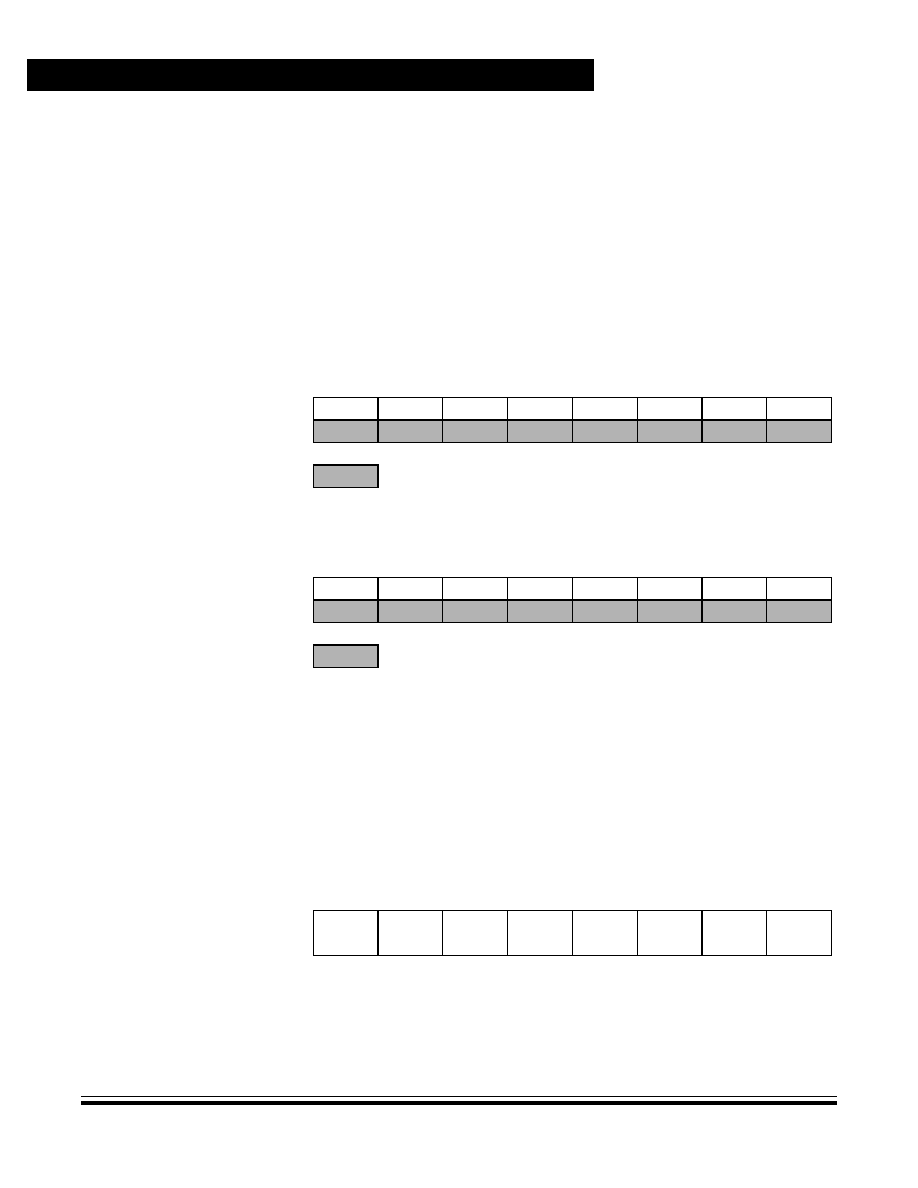
Timer Interface Module (TIM)
Data Sheet
MC68HC908GR16 -- Rev. 1.0
258
Timer Interface Module (TIM)
MOTOROLA
18.9.2 TIM Counter Registers
The two read-only TIM counter registers contain the high and low bytes of the value
in the TIM counter. Reading the high byte (TCNTH) latches the contents of the low
byte (TCNTL) into a buffer. Subsequent reads of TCNTH do not affect the latched
TCNTL value until TCNTL is read. Reset clears the TIM counter registers. Setting
the TIM reset bit (TRST) also clears the TIM counter registers.
NOTE:
If you read TCNTH during a break interrupt, be sure to unlatch TCNTL by reading
TCNTL before exiting the break interrupt. Otherwise, TCNTL retains the value
latched during the break.
18.9.3 TIM Counter Modulo Registers
The read/write TIM modulo registers contain the modulo value for the TIM counter.
When the TIM counter reaches the modulo value, the overflow flag (TOF) becomes
set, and the TIM counter resumes counting from $0000 at the next timer clock.
Writing to the high byte (TMODH) inhibits the TOF bit and overflow interrupts until
the low byte (TMODL) is written. Reset sets the TIM counter modulo registers.
Address: T1CNTH, $0021 and T2CNTH, $002C
Bit 7
6
5
4
3
2
1
Bit 0
Read:
Bit 15
14
13
12
11
10
9
Bit 8
Write:
Reset:
0
0
0
0
0
0
0
0
= Unimplemented
Figure 18-6. TIM Counter Registers High (TCNTH)
Address: T1CNTL, $0022 and T2CNTL, $002D
Bit 7
6
5
4
3
2
1
Bit 0
Read:
Bit 7
6
5
4
3
2
1
Bit 0
Write:
Reset:
0
0
0
0
0
0
0
0
= Unimplemented
Figure 18-7. TIM Counter Registers Low (TCNTL)
Address: T1MODH, $0023 and T2MODH, $002E
Bit 7
6
5
4
3
2
1
Bit 0
Read:
Bit 15
14
13
12
11
10
9
Bit 8
Write:
Reset:
1
1
1
1
1
1
1
1
Figure 18-8. TIM Counter Modulo Register High (TMODH)
Timer Interface Module (TIM)
I/O Registers
MC68HC908GR16 -- Rev. 1.0
Data Sheet
MOTOROLA
Timer Interface Module (TIM)
259
NOTE:
Reset the TIM counter before writing to the TIM counter modulo registers.
18.9.4 TIM Channel Status and Control Registers
Each of the TIM channel status and control registers:
�
Flags input captures and output compares
�
Enables input capture and output compare interrupts
�
Selects input capture, output compare, or PWM operation
�
Selects high, low, or toggling output on output compare
�
Selects rising edge, falling edge, or any edge as the active input capture
trigger
�
Selects output toggling on TIM overflow
�
Selects 0% and 100% PWM duty cycle
�
Selects buffered or unbuffered output compare/PWM operation
CHxF -- Channel x Flag Bit
When channel x is an input capture channel, this read/write bit is set when an
active edge occurs on the channel x pin. When channel x is an output compare
channel, CHxF is set when the value in the TIM counter registers matches the
value in the TIM channel x registers.
Address: T1MODL, $0024 and T2MODL, $002F
Bit 7
6
5
4
3
2
1
Bit 0
Read:
Bit 7
6
5
4
3
2
1
Bit 0
Write:
Reset:
1
1
1
1
1
1
1
1
Figure 18-9. TIM Counter Modulo Register Low (TMODL)
Address: T1SC0, $0025 and T2SC0, $0030
Bit 7
6
5
4
3
2
1
Bit 0
Read:
CH0F
CH0IE
MS0B
MS0A
ELS0B
ELS0A
TOV0
CH0MAX
Write:
0
Reset:
0
0
0
0
0
0
0
0
Figure 18-10. TIM Channel 0 Status and Control Register (TSC0)
Address: T1SC1, $0028 and T2SC1, $0033
Bit 7
6
5
4
3
2
1
Bit 0
Read:
CH1F
CH1IE
0
MS1A
ELS1B
ELS1A
TOV1
CH1MAX
Write:
0
Reset:
0
0
0
0
0
0
0
0
Figure 18-11. TIM Channel 1 Status and Control Register (TSC1)

Timer Interface Module (TIM)
Data Sheet
MC68HC908GR16 -- Rev. 1.0
260
Timer Interface Module (TIM)
MOTOROLA
When TIM CPU interrupt requests are enabled (CHxIE = 1), clear CHxF by
reading TIM channel x status and control register with CHxF set and then writing
a logic 0 to CHxF. If another interrupt request occurs before the clearing
sequence is complete, then writing logic 0 to CHxF has no effect. Therefore, an
interrupt request cannot be lost due to inadvertent clearing of CHxF.
Reset clears the CHxF bit. Writing a logic 1 to CHxF has no effect.
1 = Input capture or output compare on channel x
0 = No input capture or output compare on channel x
CHxIE -- Channel x Interrupt Enable Bit
This read/write bit enables TIM CPU interrupt service requests on channel x.
Reset clears the CHxIE bit.
1 = Channel x CPU interrupt requests enabled
0 = Channel x CPU interrupt requests disabled
MSxB -- Mode Select Bit B
This read/write bit selects buffered output compare/PWM operation. MSxB
exists only in the TIM1 channel 0 and TIM2 channel 0 status and control
registers.
Setting MS0B disables the channel 1 status and control register and reverts
TCH1 to general-purpose I/O.
Reset clears the MSxB bit.
1 = Buffered output compare/PWM operation enabled
0 = Buffered output compare/PWM operation disabled
MSxA -- Mode Select Bit A
When ELSxB:A
00, this read/write bit selects either input capture operation or
unbuffered output compare/PWM operation. See
Table 18-3
.
1 = Unbuffered output compare/PWM operation
0 = Input capture operation
When ELSxB:A = 00, this read/write bit selects the initial output level of the
TCHx pin. See
Table 18-3
. Reset clears the MSxA bit.
1 = Initial output level low
0 = Initial output level high
NOTE:
Before changing a channel function by writing to the MSxB or MSxA bit, set the
TSTOP and TRST bits in the TIM status and control register (TSC).
ELSxB and ELSxA -- Edge/Level Select Bits
When channel x is an input capture channel, these read/write bits control the
active edge-sensing logic on channel x.
When channel x is an output compare channel, ELSxB and ELSxA control the
channel x output behavior when an output compare occurs.
When ELSxB and ELSxA are both clear, channel x is not connected to port D,
and pin PTDx/TCHx is available as a general-purpose I/O pin.
Table 18-3
shows how ELSxB and ELSxA work. Reset clears the ELSxB and ELSxA bits.
Timer Interface Module (TIM)
I/O Registers
MC68HC908GR16 -- Rev. 1.0
Data Sheet
MOTOROLA
Timer Interface Module (TIM)
261
NOTE:
Before enabling a TIM channel register for input capture operation, make sure that
the PTD/TCHx pin is stable for at least two bus clocks.
TOVx -- Toggle On Overflow Bit
When channel x is an output compare channel, this read/write bit controls the
behavior of the channel x output when the TIM counter overflows. When
channel x is an input capture channel, TOVx has no effect. Reset clears the
TOVx bit.
1 = Channel x pin toggles on TIM counter overflow.
0 = Channel x pin does not toggle on TIM counter overflow.
NOTE:
When TOVx is set, a TIM counter overflow takes precedence over a channel x
output compare if both occur at the same time.
CHxMAX -- Channel x Maximum Duty Cycle Bit
When the TOVx bit is at logic 1, setting the CHxMAX bit forces the duty cycle of
buffered and unbuffered PWM signals to 100%. As
Figure 18-12
shows, the
CHxMAX bit takes effect in the cycle after it is set or cleared. The output stays
at the 100% duty cycle level until the cycle after CHxMAX is cleared.
Figure 18-12. CHxMAX Latency
Table 18-3. Mode, Edge, and Level Selection
MSxB:MSxA
ELSxB:ELSxA
Mode
Configuration
X0
00
Output
preset
Pin under port control; initial output level high
X1
00
Pin under port control; initial output level low
00
01
Input
capture
Capture on rising edge only
00
10
Capture on falling edge only
00
11
Capture on rising or falling edge
01
01
Output compare
or PWM
Toggle output on compare
01
10
Clear output on compare
01
11
Set output on compare
1X
01
Buffered output
compare
or buffered
PWM
Toggle output on compare
1X
10
Clear output on compare
1X
11
Set output on compare
OUTPUT
OVERFLOW
TCHx
PERIOD
CHxMAX
OVERFLOW
OVERFLOW
OVERFLOW
OVERFLOW
COMPARE
OUTPUT
COMPARE
OUTPUT
COMPARE
OUTPUT
COMPARE
Timer Interface Module (TIM)
Data Sheet
MC68HC908GR16 -- Rev. 1.0
262
Timer Interface Module (TIM)
MOTOROLA
18.9.5 TIM Channel Registers
These read/write registers contain the captured TIM counter value of the input
capture function or the output compare value of the output compare function. The
state of the TIM channel registers after reset is unknown.
In input capture mode (MSxB:MSxA = 0:0), reading the high byte of the TIM
channel x registers (TCHxH) inhibits input captures until the low byte (TCHxL) is
read.
In output compare mode (MSxB:MSxA
0:0), writing to the high byte of the TIM
channel x registers (TCHxH) inhibits output compares until the low byte (TCHxL) is
written.
Address: T1CH0H, $0026 and T2CH0H, $0031
Bit 7
6
5
4
3
2
1
Bit 0
Read:
Bit 15
14
13
12
11
10
9
Bit 8
Write:
Reset:
Indeterminate after reset
Figure 18-13. TIM Channel 0 Register High (TCH0H)
Address: T1CH0L, $0027 and T2CH0L $0032
Bit 7
6
5
4
3
2
1
Bit 0
Read:
Bit 7
6
5
4
3
2
1
Bit 0
Write:
Reset:
Indeterminate after reset
Figure 18-14. TIM Channel 0 Register Low (TCH0L)
Address: T1CH1H, $0029 and T2CH1H, $0034
Bit 7
6
5
4
3
2
1
Bit 0
Read:
Bit 15
14
13
12
11
10
9
Bit 8
Write:
Reset:
Indeterminate after reset
Figure 18-15. TIM Channel 1 Register High (TCH1H)
Address: T1CH1L, $002A and T2CH1L, $0035
Bit 7
6
5
4
3
2
1
Bit 0
Read:
Bit 7
6
5
4
3
2
1
Bit 0
Write:
Reset:
Indeterminate after reset
Figure 18-16. TIM Channel 1 Register Low (TCH1L)

MC68HC908GR16 -- Rev. 1.0
Data Sheet
MOTOROLA
Development Support
263
Data Sheet -- MC68HC908GR16
Section 19. Development Support
19.1 Introduction
This section describes the break module, the monitor read-only memory (MON),
and the monitor mode entry methods.
19.2 Break Module (BRK)
This subsection describes the break module. The break module can generate a
break interrupt that stops normal program flow at a defined address to enter a
background program.
Features of the break module include:
�
Accessible input/output (I/O) registers during the break Interrupt
�
Central processor unit (CPU) generated break interrupts
�
Software-generated break interrupts
�
Computer operating properly (COP) disabling during break interrupts
19.2.1 Functional Description
When the internal address bus matches the value written in the break address
registers, the break module issues a breakpoint signal (BKPT) to the system
integration module (SIM). The SIM then causes the CPU to load the instruction
register with a software interrupt instruction (SWI) after completion of the current
CPU instruction. The program counter vectors to $FFFC and $FFFD ($FEFC and
$FEFD in monitor mode).
The following events can cause a break interrupt to occur:
�
A CPU generated address (the address in the program counter) matches
the contents of the break address registers.
�
Software writes a logic 1 to the BRKA bit in the break status and control
register.
When a CPU generated address matches the contents of the break address
registers, the break interrupt begins after the CPU completes its current instruction.
A return-from-interrupt instruction (RTI) in the break routine ends the break
interrupt and returns the microcontroller unit (MCU) to normal operation.
Figure 19-1
shows the structure of the break module.
Figure 19-2
provides a summary of the I/O registers.
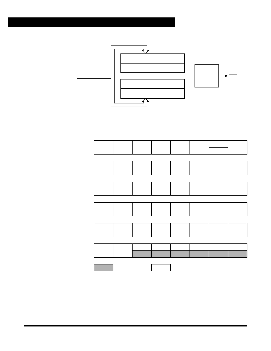
Development Support
Data Sheet
MC68HC908GR16 -- Rev. 1.0
264
Development Support
MOTOROLA
Figure 19-1. Break Module Block Diagram
ADDRESS BUS[15:8]
ADDRESS BUS[7:0]
8-BIT COMPARATOR
8-BIT COMPARATOR
CONTROL
BREAK ADDRESS REGISTER LOW
BREAK ADDRESS REGISTER HIGH
ADDRESS BUS[15:0]
BKPT
(TO SIM)
Addr.
Register Name
Bit 7
6
5
4
3
2
1
Bit 0
$FE00
Break Status Register
(BSR)
See page 267.
Read:
R
R
R
R
R
R
SBSW
R
Write:
Note
(1)
Reset:
0
$FE02
Break Auxiliary Register
(BRKAR)
See page 267.
Read:
Bit 7
Bit 6
Bit 5
Bit 4
Bit 3
Bit 2
Bit 1
Bit 0
Write:
Reset:
0
0
0
0
0
0
0
0
$FE03
Break Flag Control
Register (BFCR)
See page 268.
Read:
BCFE
R
R
R
R
R
R
R
Write:
Reset:
0
$FE09
Break Address High
Register (BRKH)
See page 266.
Read:
Bit15
Bit14
Bit13
Bit12
Bit11
Bit10
Bit9
Bit8
Write:
Reset:
0
0
0
0
0
0
0
0
$FE0A
Break Address Low
Register (BRKL)
See page 266.
Read:
Bit 7
Bit 6
Bit 5
Bit 4
Bit 3
Bit 2
Bit 1
Bit 0
Write:
Reset:
0
0
0
0
0
0
0
0
$FE0B
Break Status and Control
Register (BRKSCR)
See page 266.
Read:
BRKE
BRKA
0
0
0
0
0
0
Write:
Reset:
0
0
0
0
0
0
0
0
1. Writing a logic 0 clears SBSW.
= Unimplemented
R
= Reserved
Figure 19-2. Break I/O Register Summary

Development Support
Break Module (BRK)
MC68HC908GR16 -- Rev. 1.0
Data Sheet
MOTOROLA
Development Support
265
19.2.1.1 Flag Protection During Break Interrupts
The system integration module (SIM) controls whether or not module status bits
can be cleared during the break state. The BCFE bit in the break flag control
register (BFCR) enables software to clear status bits during the break state. See
15.7.3 Break Flag Control Register
and the Break Interrupts subsection for
each module.
19.2.1.2 CPU During Break Interrupts
The CPU starts a break interrupt by:
�
Loading the instruction register with the SWI instruction
�
Loading the program counter with $FFFC:$FFFD ($FEFC:$FEFD in monitor
mode)
The break interrupt begins after completion of the CPU instruction in progress. If
the break address register match occurs on the last cycle of a CPU instruction, the
break interrupt begins immediately.
19.2.1.3 TIM During Break Interrupts
A break interrupt stops the timer counter.
19.2.1.4 COP During Break Interrupts
The COP is disabled during a break interrupt with monitor mode when BDCOP bit
is set in break auxiliary register (BRKAR).
19.2.2 Break Module Registers
These registers control and monitor operation of the break module:
�
Break status and control register (BRKSCR)
�
Break address register high (BRKH)
�
Break address register low (BRKL)
�
Break status register (BSR)
�
Break flag control register (BFCR)
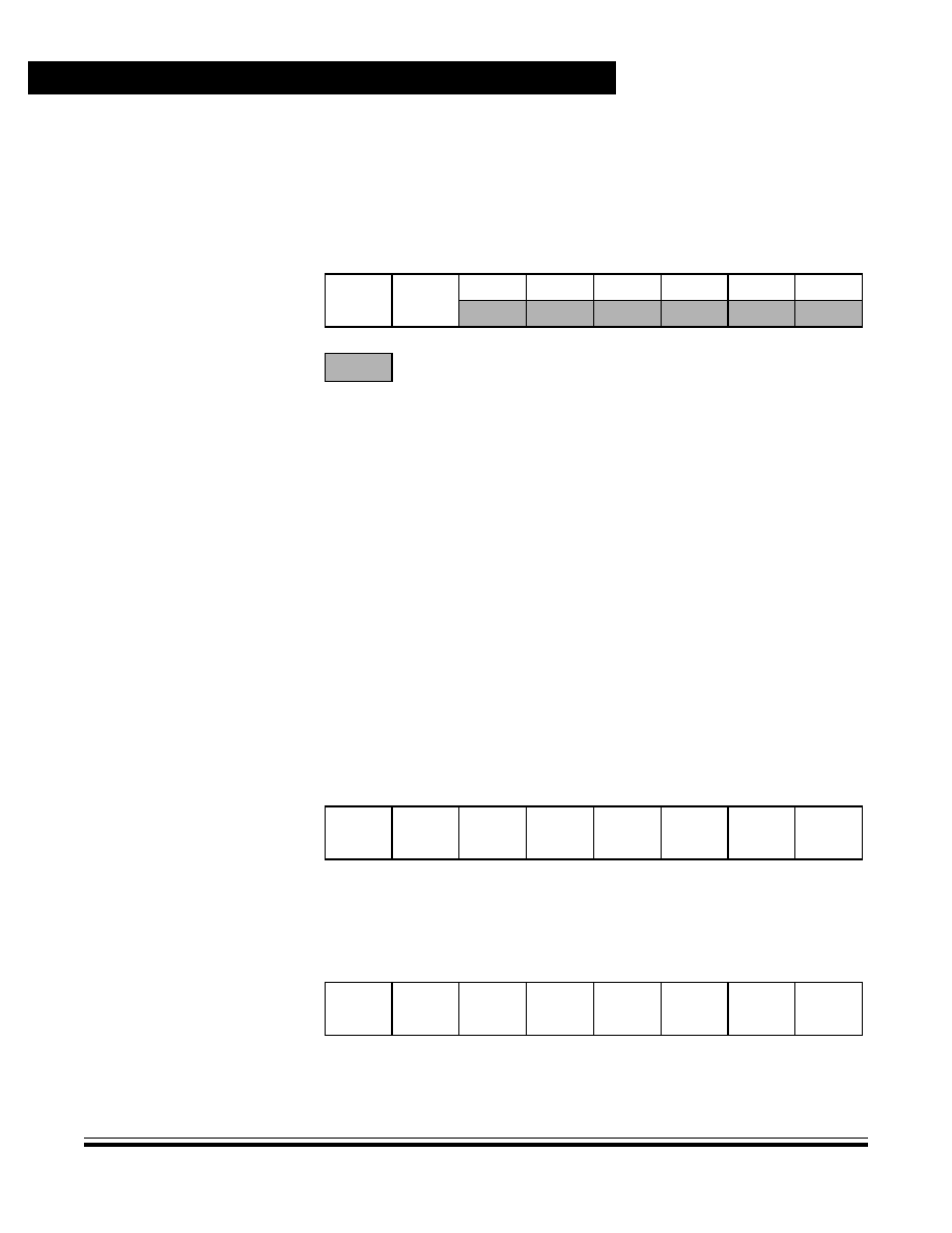
Development Support
Data Sheet
MC68HC908GR16 -- Rev. 1.0
266
Development Support
MOTOROLA
19.2.2.1 Break Status and Control Register
The break status and control register (BRKSCR) contains break module enable
and status bits.
BRKE -- Break Enable Bit
This read/write bit enables breaks on break address register matches. Clear
BRKE by writing a logic 0 to bit 7. Reset clears the BRKE bit.
1 = Breaks enabled on 16-bit address match
0 = Breaks disabled
BRKA -- Break Active Bit
This read/write status and control bit is set when a break address match occurs.
Writing a logic 1 to BRKA generates a break interrupt. Clear BRKA by writing a
logic 0 to it before exiting the break routine. Reset clears the BRKA bit.
1 = Break address match
0 = No break address match
19.2.2.2 Break Address Registers
The break address registers (BRKH and BRKL) contain the high and low bytes of
the desired breakpoint address. Reset clears the break address registers.
Address: $FE0B
Bit 7
6
5
4
3
2
1
Bit 0
Read:
BRKE
BRKA
0
0
0
0
0
0
Write:
Reset:
0
0
0
0
0
0
0
0
= Unimplemented
Figure 19-3. Break Status and Control Register (BRKSCR)
Address: $FE09
Bit 7
6
5
4
3
2
1
Bit 0
Read:
Bit 15
Bit 14
Bit 13
Bit 12
Bit 11
Bit 10
Bit 9
Bit 8
Write:
Reset:
0
0
0
0
0
0
0
0
Figure 19-4. Break Address Register High (BRKH)
Address: $FE0A
Bit 7
6
5
4
3
2
1
Bit 0
Read:
Bit 7
Bit 6
Bit 5
Bit 4
Bit 3
Bit 2
Bit 1
Bit 0
Write:
Reset:
0
0
0
0
0
0
0
0
Figure 19-5. Break Address Register Low (BRKL)
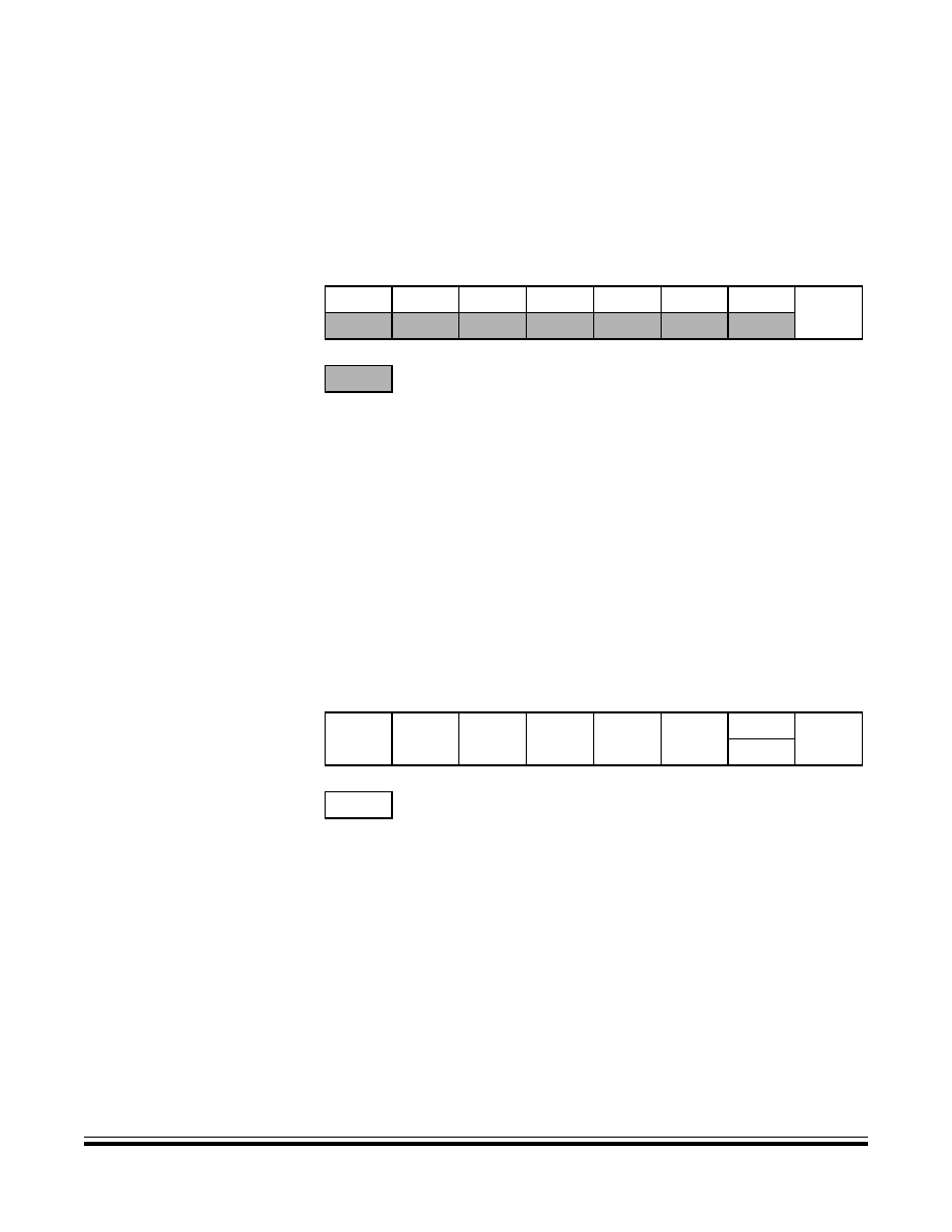
Development Support
Break Module (BRK)
MC68HC908GR16 -- Rev. 1.0
Data Sheet
MOTOROLA
Development Support
267
19.2.2.3 Break Auxiliary Register
The break auxiliary register (BRKAR) contains a bit that enables software to
disable the COP while the MCU is in a state of break interrupt with monitor mode.
BDCOP -- Break Disable COP Bit
This read/write bit disables the COP during a break interrupt. Reset clears the
BDCOP bit.
1 = COP disabled during break interrupt
0 = COP enabled during break interrupt.
19.2.2.4 Break Status Register
The break status register (BSR) contains a flag to indicate that a break caused an
exit from wait mode. This register is only used in emulation mode.
SBSW -- SIM Break Stop/Wait
This status bit is useful in applications requiring a return to wait mode after
exiting from a break interrupt. Clear SBSW by writing a logic 0 to it. Reset clears
SBSW.
1 = Wait mode was exited by break interrupt
0 = Wait mode was not exited by break interrupt
SBSW can be read within the break state SWI routine. The user can modify the
return address on the stack by subtracting one from it.
Address: $FE02
Bit 7
6
5
4
3
2
1
Bit 0
Read:
0
0
0
0
0
0
0
BDCOP
Write:
Reset:
0
0
0
0
0
0
0
0
= Unimplemented
Figure 19-6. Break Auxiliary Register (BRKAR)
Address: $FE00
Bit 7
6
5
4
3
2
1
Bit 0
Read:
R
R
R
R
R
R
SBSW
R
Write:
Note
(1)
Reset:
0
R
= Reserved
1. Writing a logic 0 clears SBSW.
Figure 19-7. Break Status Register (BSR)

Development Support
Data Sheet
MC68HC908GR16 -- Rev. 1.0
268
Development Support
MOTOROLA
19.2.2.5 Break Flag Control Register
The break control register (BFCR) contains a bit that enables software to clear
status bits while the MCU is in a break state.
BCFE -- Break Clear Flag Enable Bit
This read/write bit enables software to clear status bits by accessing status
registers while the MCU is in a break state. To clear status bits during the break
state, the BCFE bit must be set.
1 = Status bits clearable during break
0 = Status bits not clearable during break
19.2.3 Low-Power Modes
The WAIT and STOP instructions put the MCU in low power- consumption standby
modes. If enabled, the break module will remain enabled in wait and stop modes.
However, since the internal address bus does not increment in these modes, a
break interrupt will never be triggered.
19.3 Monitor ROM (MON)
This section describes the monitor ROM (MON) and the monitor mode entry
methods. The monitor ROM allows complete testing of the microcontroller unit
(MCU) through a single-wire interface with a host computer. Monitor mode entry
can be achieved without use of the higher test voltage, V
TST
, as long as vector
addresses $FFFE and $FFFF are blank, thus reducing the hardware requirements
for in-circuit programming.
Features of the monitor ROM include:
�
Normal user-mode pin functionality
�
One pin dedicated to serial communication between monitor read-only
memory (ROM) and host computer
�
Standard mark/space non-return-to-zero (NRZ) communication with host
computer
�
Standard communication baud rate (9,600 @ 2.4576-MHz bus frequency)
Address: $FE03
Bit 7
6
5
4
3
2
1
Bit 0
Read:
BCFE
R
R
R
R
R
R
R
Write:
Reset:
0
R
= Reserved
Figure 19-8. Break Flag Control Register (BFCR)

Development Support
Monitor ROM (MON)
MC68HC908GR16 -- Rev. 1.0
Data Sheet
MOTOROLA
Development Support
269
�
Execution of code in random-access memory (RAM) or FLASH
�
FLASH memory security feature
(1)
�
FLASH memory programming interface
�
350 bytes monitor ROM code size ($FE20 to $FF6A)
�
Monitor mode entry without high voltage, V
TST
, if reset vector is blank
($FFFE and $FFFF contain $FF)
�
Normal monitor mode entry if high voltage is applied to IRQ
19.3.1 Functional Description
Figure 19-9
shows a simplified diagram of the monitor mode.
The monitor ROM receives and executes commands from a host computer.
Figure 19-10
and
Figure 19-11
show example circuits used to enter monitor mode
and communicate with a host computer via a standard RS-232 interface.
Simple monitor commands can access any memory address. In monitor mode, the
MCU can execute code downloaded into RAM by a host computer while most MCU
pins retain normal operating mode functions. All communication between the host
computer and the MCU is through the PTA0 pin. A level-shifting and multiplexing
interface is required between PTA0 and the host computer. PTA0 is used in a
wired-OR configuration and requires a pullup resistor.
Table 19-1
shows the pin conditions for entering monitor mode. As specified in the
table, monitor mode may be entered after a power-on reset (POR) and will allow
communication at 14,400 baud provided one of the following sets of conditions is
met:
�
If $FFFE and $FFFF does not contain $FF (programmed state):
�
The external clock is 4.9152 MHz
�
PTB4 = low
�
IRQ = V
TST
�
If $FFFE and $FFFF do not contain $FF (programmed state):
�
The external clock is 9.8304 MHz
�
PTB4 = high
�
IRQ = V
TST
�
If $FFFE and $FFFF contain $FF (erased state):
�
The external clock is 32.768 kHz
�
IRQ = V
SS
The last two conditions are the forced monitor mode.
1. No security feature is absolutely secure. However, Motorola's strategy is to make reading or
copying the FLASH difficult for unauthorized users.
Development Support
Data Sheet
MC68HC908GR16 -- Rev. 1.0
270
Development Support
MOTOROLA
Figure 19-9. Simplified Monitor Mode Entry Flowchart
MONITOR MODE ENTRY
POR RESET
PTA0 = 1, PTA1 = 0,
PTB0 = 1, AND
PTB1 = 0?
IRQ = V
TST
?
PTA0 = 1,
PTA1 = 0, RESET
BLANK?
YES
NO
YES
NO
FORCED
MONITOR MODE
NORMAL
USER MODE
NORMAL
MONITOR MODE
FACTORY
USE ONLY
NO
NO
SEND 8 BYTES
SECURITY
IS RESET
POR?
YES
YES
YES
NO
ARE ALL
SECURITY BYTES
CORRECT?
NO
YES
ENABLE FLASH
DISABLE FLASH
EXECUTE
MONITOR CODE
DOES RESET
OCCUR?
CONDITIONS
FROM
Table 19-1
DEBUGGING
AND FLASH
PROGRAMMING
(IF FLASH
IS ENABLED)
Development Support
Monitor ROM (MON)
MC68HC908GR16 -- Rev. 1.0
Data Sheet
MOTOROLA
Development Support
271
Figure 19-10. Normal Monitor Mode Circuit
Figure 19-11. Forced Monitor Mode Circuit (IRQ = V
DD
)
10 k
10 k
10 k
10 k
RST
IRQ
PTA0
OSC1
8
7
DB9
2
3
5
16
15
2
6
10
9
V
DD
C5
MAX232
V+
V�
V
DD
C4
+
1
2
3
4
5
6
74HC125
74HC125
10 k
V
SS
0.1
�F
V
DD
C1+
C1�
5
4
1
�F
C2+
C2�
+
3
1
1
�F
+
+
+
C3
V
DD
N.C.
V
CC
GND
1 k
OSC2
47 pF
27 pF
9.8304 MHz
10 M
V
DDA
PTB4
PTB0
PTB1
PTA1
V
SSA
V
DD
MC68HC908GR16
V
TST
10 k
RST
IRQ
PTA0
OSC1
8
7
DB9
2
3
5
16
15
2
6
10
9
V
DD
C5
MAX232
V+
V�
V
DD
C4
+
1
2
3
4
5
6
74HC125
74HC125
10 k
V
SS
0.1
�F
V
DD
C1+
C1�
5
4
1
�F
C2+
C2�
+
3
1
1
�F
+
+
+
C3
V
DD
N.C.
V
CC
GND
OSC2
47 pF
27 pF
9.8304 MHz
10 M
V
DDA
PTB4
PTB0
PTB1
PTA1
V
SSA
MC68HC908GR16
N.C.
N.C.
N.C.
N.C.
Development Support
Data Sheet
MC68HC908GR16 -- Rev. 1.0
272
Development Support
MOTOROLA
Figure 19-12. Forced Monitor Mode Circuit (IRQ = GND)
Enter monitor mode with pin configuration shown in
Table 19-1
by pulling RST low
and then high. The rising edge of RST latches monitor mode. Once monitor mode
is latched, the values on the specified pins can change.
Once out of reset, the MCU waits for the host to send eight security bytes (see
19.3.2 Security
). After the security bytes, the MCU sends a break signal (10
consecutive logic 0s) to the host, indicating that it is ready to receive a command.
19.3.1.1 Normal Monitor Mode
Table 19-1
shows the pin conditions for entering monitor mode.
If V
TST
is applied to IRQ and PTB4 is low upon monitor mode entry, the bus
frequency is a divide-by-two of the input clock. If PTB4 is high with V
TST
applied to
IRQ upon monitor mode entry, the bus frequency will be a divide-by-four of the
input clock. Holding the PTB4 pin low when entering monitor mode causes a
bypass of a divide-by-two stage at the oscillator only if V
TST
is applied to IRQ. In
this event, the CGMOUT frequency is equal to the CGMXCLK frequency, and the
OSC1 input directly generates internal bus clocks. In this case, the OSC1 signal
must have a 50% duty cycle at maximum bus frequency.
When monitor mode was entered with V
TST
on IRQ, the computer operating
properly (COP) is disabled as long as V
TST
is applied to either IRQ or RST.
10 k
RST
IRQ
PTA0
OSC1
8
7
DB9
2
3
5
16
15
2
6
10
9
V
DD
C5
MAX232
V+
V�
V
DD
C4
+
1
2
3
4
5
6
74HC125
74HC125
10 k
V
SS
0.1
�F
V
DD
C1+
C1�
5
4
1
�F
C2+
C2�
+
3
1
1
�F
+
+
+
C3
V
DD
N.C.
V
CC
GND
OSC2
33 pF
15 pF
32.768 kHz
10 M
V
DDA
PTB4
PTB0
PTB1
PTA1
V
SSA
MC68HC908GR16
N.C.
N.C.
N.C.
10 k
4.7 k
MC68HC
908
GR16
--
Rev. 1
.
0
Data Sheet
MOTOROLA
Devel
opment Supp
ort
2
73
De
ve
lo
pm
e
n
t Su
pp
or
t
M
o
n
i
to
r RO
M (M
ON
)
Table 19-1. Monitor Mode Signal Requirements and Options
Mode
IRQ
RST
Reset
Vector
Serial
Communication
Mode
Selection
Divider
PLL
COP
Communication
Speed
Comments
PTA0
PTA1
PTB0
PTB1
PTB4
External
Clock
Bus
Frequency
Baud
Rate
--
X
GND
X
X
X
X
X
X
X
X
X
X
X
Reset condition
Normal
Monitor
V
TST
V
DD
or
V
TST
X
1
0
1
0
0
OFF Disabled
4.9152
MHz
2.4576
MHz
9600
V
TST
V
DD
or
V
TST
X
1
0
1
0
1
OFF Disabled
9.8304
MHz
2.4576
MHz
9600
Forced
Monitor
V
DD
V
DD
$FF
(blank)
1
0
X
X
X
OFF Disabled
16 MHz
4 MHz
9600
GND
V
DD
$FF
(blank)
1
0
X
X
X
ON
Disabled
32.768
kHz
2.4576
MHz
9600
User
V
DD
or
GND
V
DD
or
V
TST
$FF
(blank)
X
X
X
X
X
OFF Enabled
X
X
X
User mode --
illegal address reset
V
DD
or
GND
V
DD
or
V
TST
Not
$FF
X
X
X
X
X
X
Enabled
X
X
X
MON08
Function
[Pin No.]
V
TST
[6]
RST
[5]
--
COM
[8]
SSEL
[10]
MOD0
[12]
MOD1
[14]
DIV4
[16]
--
--
OSC1
[13]
--
--
1. PTA0 must have a pullup resistor to V
DD
in monitor mode.
2. Communication speed in the table is an example to obtain a baud rate of 9600. Baud rate using external oscillator is bus frequency / 256.
3. External clock is an 32.768 kHz crystal on OSC1 and OSC2 or a 32.768 kHz, 4.9152 MHz, or 9.8304 MHz canned oscillator on OSC1.
4. X = don't care
5. MON08 pin refers to P&E Microcomputer Systems' MON08-Cyclone 2 by 8-pin connector.
NC
1
2
GND
NC
3
4
RST
NC
5
6
IRQ
NC
7
8
PTA0
NC
9
10
PTA1
NC
11
12
PTB0
OSC1
13
14
PTB1
V
DD
15
16
PTB4

Development Support
Data Sheet
MC68HC908GR16 -- Rev. 1.0
274
Development Support
MOTOROLA
This condition states that as long as V
TST
is maintained on the IRQ pin after
entering monitor mode, or if V
TST
is applied to RST after the initial reset to get into
monitor mode (when V
TST
was applied to IRQ), then the COP will be disabled. In
the latter situation, after V
TST
is applied to the RST pin, V
TST
can be removed from
the IRQ pin in the interest of freeing the IRQ for normal functionality in monitor
mode.
19.3.1.2 Forced Monitor Mode
If entering monitor mode without high voltage on IRQ, then all port B pin
requirements and conditions, including the PTB4 frequency divisor selection, are
not in effect. This is to reduce circuit requirements when performing in-circuit
programming.
NOTE:
Once the reset vector has been programmed, the traditional method of applying a
voltage, V
TST
, to IRQ must be used to enter monitor mode.
An external oscillator of 9.8304 MHz is required for a baud rate of 9600, as the
internal bus frequency is automatically set to the external frequency divided by
four.
When the forced monitor mode is entered the COP is always disabled regardless
of the state of IRQ or RST.
19.3.1.3 Monitor Vectors
In monitor mode, the MCU uses different vectors for reset, SWI (software interrupt),
and break interrupt than those for user mode. The alternate vectors are in the $FE
page instead of the $FF page and allow code execution from the internal monitor
firmware instead of user code.
Table 19-2
summarizes the differences between user mode and monitor mode.
Table 19-2. Mode Differences
Modes
Functions
Reset
Vector High
Reset
Vector Low
Break
Vector High
Break
Vector Low
SWI
Vector High
SWI
Vector Low
User
$FFFE
$FFFF
$FFFC
$FFFD
$FFFC
$FFFD
Monitor
$FEFE
$FEFF
$FEFC
$FEFD
$FEFC
$FEFD
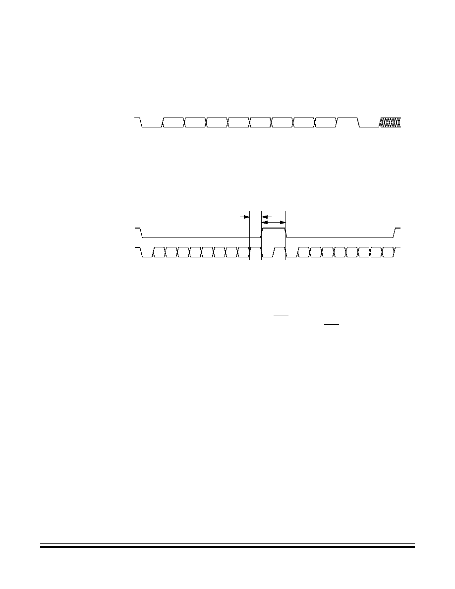
Development Support
Monitor ROM (MON)
MC68HC908GR16 -- Rev. 1.0
Data Sheet
MOTOROLA
Development Support
275
19.3.1.4 Data Format
Communication with the monitor ROM is in standard non-return-to-zero (NRZ)
mark/space data format. Transmit and receive baud rates must be identical.
Figure 19-13. Monitor Data Format
19.3.1.5 Break Signal
A start bit (logic 0) followed by nine logic 0 bits is a break signal. When the monitor
receives a break signal, it drives the PTA0 pin high for the duration of two bits and
then echoes back the break signal.
Figure 19-14. Break Transaction
19.3.1.6 Baud Rate
The communication baud rate is controlled by the crystal frequency or external
clock and the state of the PTB4 pin (when IRQ is set to V
TST
) upon entry into
monitor mode. If monitor mode was entered with V
DD
on IRQ and the reset vector
blank, then the baud rate is independent of PTB4.
Table 19-1
also lists external frequencies required to achieve a standard baud rate
of 9600 bps. The effective baud rate is the bus frequency divided by 256. If using
a crystal as the clock source, be aware of the upper frequency limit that the internal
clock module can handle. See
20.7 5.0-Volt Control Timing
or
20.8 3.3-Volt
Control Timing
for this limit.
BIT 5
START
BIT
BIT 1
NEXT
STOP
BIT
START
BIT
BIT 2
BIT 3
BIT 4
BIT 7
BIT 0
BIT 6
0
1
2
3
4
5
6
7
0
1
2
3
4
5
6
7
MISSING STOP BIT
2-STOP BIT DELAY BEFORE ZERO ECHO
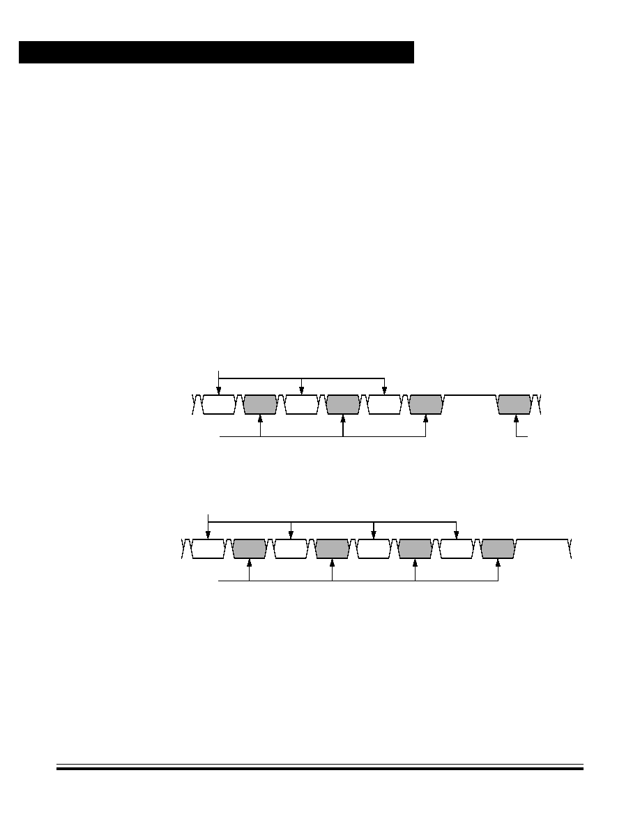
Development Support
Data Sheet
MC68HC908GR16 -- Rev. 1.0
276
Development Support
MOTOROLA
19.3.1.7 Commands
The monitor ROM firmware uses these commands:
�
READ (read memory)
�
WRITE (write memory)
�
IREAD (indexed read)
�
IWRITE (indexed write)
�
READSP (read stack pointer)
�
RUN (run user program)
The monitor ROM firmware echoes each received byte back to the PTA0 pin for
error checking. An 11-bit delay at the end of each command allows the host to send
a break character to cancel the command. A delay of two bit times occurs before
each echo and before READ, IREAD, or READSP data is returned. The data
returned by a read command appears after the echo of the last byte of the
command.
NOTE:
Wait one bit time after each echo before sending the next byte.
Figure 19-15. Read Transaction
Figure 19-16. Write Transaction
READ
READ
ECHO
FROM HOST
ADDRESS
HIGH
ADDRESS
HIGH
ADDRESS
LOW
ADDRESS
LOW
DATA
RETURN
1
3, 2
1
1
4
4
Notes:
2 = Data return delay, 2 bit times
4
4
1 = Echo delay, 2 bit times
3 = Cancel command delay, 11 bit times
4 = Wait 1 bit time before sending next byte.
WRITE
WRITE
ECHO
FROM HOST
ADDRESS
HIGH
ADDRESS
HIGH
ADDRESS
LOW
ADDRESS
LOW
DATA
DATA
Notes:
2 = Cancel command delay, 11 bit times
3 = Wait 1 bit time before sending next byte.
1
1
3
1
1
3
3
3
2, 3
1 = Echo delay, 2 bit times
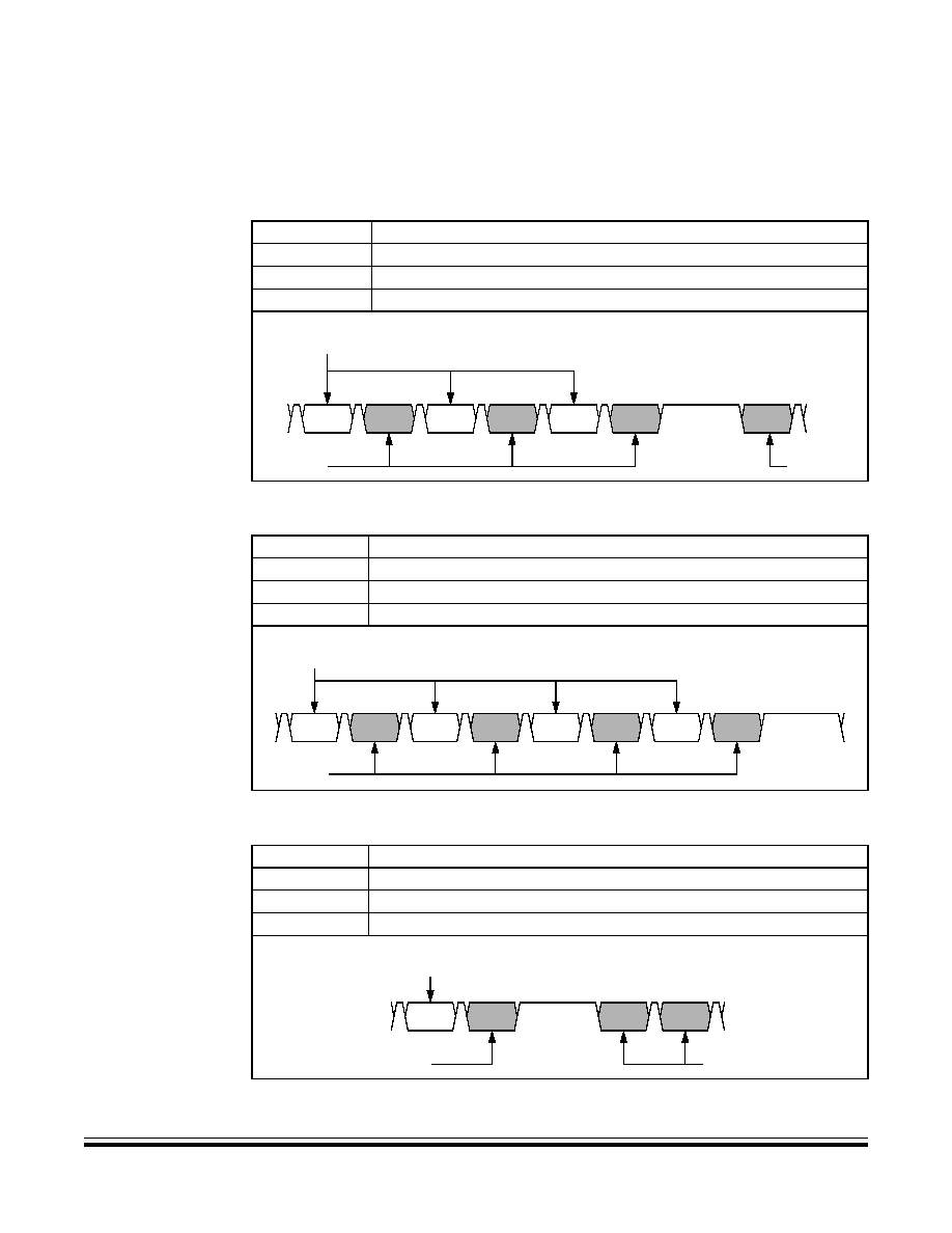
Development Support
Monitor ROM (MON)
MC68HC908GR16 -- Rev. 1.0
Data Sheet
MOTOROLA
Development Support
277
A brief description of each monitor mode command is given in
Table 19-3
through
Table 19-8
.
Table 19-3. READ (Read Memory) Command
Description
Read byte from memory
Operand
2-byte address in high-byte:low-byte order
Data Returned
Returns contents of specified address
Opcode
$4A
Command Sequence
Table 19-4. WRITE (Write Memory) Command
Description
Write byte to memory
Operand
2-byte address in high-byte:low-byte order; low byte followed by data byte
Data Returned
None
Opcode
$49
Command Sequence
Table 19-5. IREAD (Indexed Read) Command
Description
Read next 2 bytes in memory from last address accessed
Operand
2-byte address in high byte:low byte order
Data Returned
Returns contents of next two addresses
Opcode
$1A
Command Sequence
READ
READ
ECHO
SENT TO MONITOR
ADDRESS
HIGH
ADDRESS
HIGH
ADDRESS
LOW
DATA
RETURN
ADDRESS
LOW
WRITE
WRITE
ECHO
FROM HOST
ADDRESS
HIGH
ADDRESS
HIGH
ADDRESS
LOW
ADDRESS
LOW
DATA
DATA
IREAD
IREAD
ECHO
FROM HOST
DATA
RETURN
DATA
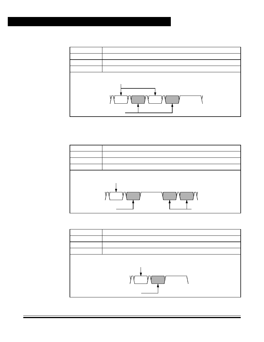
Development Support
Data Sheet
MC68HC908GR16 -- Rev. 1.0
278
Development Support
MOTOROLA
A sequence of IREAD or IWRITE commands can access a block of memory
sequentially over the full 64-Kbyte memory map.
Table 19-6. IWRITE (Indexed Write) Command
Description
Write to last address accessed + 1
Operand
Single data byte
Data Returned
None
Opcode
$19
Command Sequence
Table 19-7. READSP (Read Stack Pointer) Command
Description
Reads stack pointer
Operand
None
Data Returned
Returns incremented stack pointer value (SP + 1) in high-byte:low-byte order
Opcode
$0C
Command Sequence
Table 19-8. RUN (Run User Program) Command
Description
Executes PULH and RTI instructions
Operand
None
Data Returned
None
Opcode
$28
Command Sequence
IWRITE
IWRITE
ECHO
DATA
DATA
FROM HOST
READSP
READSP
ECHO
FROM HOST
SP
RETURN
SP
HIGH
LOW
RUN
RUN
ECHO
FROM HOST

Development Support
Monitor ROM (MON)
MC68HC908GR16 -- Rev. 1.0
Data Sheet
MOTOROLA
Development Support
279
The MCU executes the SWI and PSHH instructions when it enters monitor mode.
The RUN command tells the MCU to execute the PULH and RTI instructions.
Before sending the RUN command, the host can modify the stacked CPU registers
to prepare to run the host program. The READSP command returns the
incremented stack pointer value, SP + 1. The high and low bytes of the program
counter are at addresses SP + 5 and SP + 6.
Figure 19-17. Stack Pointer at Monitor Mode Entry
19.3.2 Security
A security feature discourages unauthorized reading of FLASH locations while in
monitor mode. The host can bypass the security feature at monitor mode entry by
sending eight security bytes that match the bytes at locations $FFF6�$FFFD.
Locations $FFF6�$FFFD contain user-defined data.
NOTE:
Do not leave locations $FFF6�$FFFD blank. For security reasons, program
locations $FFF6�$FFFD even if they are not used for vectors.
During monitor mode entry, the MCU waits after the power-on reset for the host to
send the eight security bytes on pin PTA0. If the received bytes match those at
locations $FFF6�$FFFD, the host bypasses the security feature and can read all
FLASH locations and execute code from FLASH. Security remains bypassed until
a power-on reset occurs. If the reset was not a power-on reset, security remains
bypassed and security code entry is not required. See
Figure 19-18
.
Upon power-on reset, if the received bytes of the security code do not match the
data at locations $FFF6�$FFFD, the host fails to bypass the security feature. The
MCU remains in monitor mode, but reading a FLASH location returns an invalid
value and trying to execute code from FLASH causes an illegal address reset. After
receiving the eight security bytes from the host, the MCU transmits a break
character, signifying that it is ready to receive a command.
NOTE:
The MCU does not transmit a break character until after the host sends the eight
security bytes.
CONDITION CODE REGISTER
ACCUMULATOR
LOW BYTE OF INDEX REGISTER
HIGH BYTE OF PROGRAM COUNTER
LOW BYTE OF PROGRAM COUNTER
SP + 1
SP + 2
SP + 3
SP + 4
SP + 5
SP
SP + 6
HIGH BYTE OF INDEX REGISTER
SP + 7
Development Support
Data Sheet
MC68HC908GR16 -- Rev. 1.0
280
Development Support
MOTOROLA
Figure 19-18. Monitor Mode Entry Timing
To determine whether the security code entered is correct, check to see if bit 6 of
RAM address $40 is set. If it is, then the correct security code has been entered
and FLASH can be accessed.
If the security sequence fails, the device should be reset by a power-on reset and
brought up in monitor mode to attempt another entry. After failing the security
sequence, the FLASH module can also be mass erased by executing an erase
routine that was downloaded into internal RAM. The mass erase operation clears
the security code locations so that all eight security bytes become $FF (blank).
BYTE 1
BYTE 1 ECHO
BYTE 2
BYTE 2 ECHO
BYTE 8
BY
TE 8
EC
HO
COMMAND
COMMAND
ECHO
PA0
RST
V
DD
4096 + 32 CGMXCLK CYCLES
5
1
4
1
1
2
1
BRE
AK
Notes:
2 = Data return delay, 2 bit times
4 = Wait 1 bit time before sending next byte
4
FROM HOST
FROM MCU
1 = Echo delay, 2 bit times
5 = Wait until a clock is stable (if PLL is enabled) and the monitor ROM runs
MC68HC908GR16 -- Rev. 1.0
Data Sheet
MOTOROLA
Electrical Specifications
281
Data Sheet -- MC68HC908GR16
Section 20. Electrical Specifications
20.1 Introduction
This section contains electrical and timing specifications.
20.2 Absolute Maximum Ratings
Maximum ratings are the extreme limits to which the MCU can be exposed without
permanently damaging it.
NOTE:
This device is not guaranteed to operate properly at the maximum ratings. Refer to
20.5 5.0-Vdc Electrical Characteristics
and
20.6 3.3-Vdc Electrical
Characteristics
for guaranteed operating conditions.
NOTE:
This device contains circuitry to protect the inputs against damage due to high
static voltages or electric fields; however, it is advised that normal precautions be
taken to avoid application of any voltage higher than maximum-rated voltages to
this high-impedance circuit. For proper operation, it is recommended that V
In
and
V
Out
be constrained to the range V
SS
(V
In
or V
Out
)
V
DD
. Reliability of operation
is enhanced if unused inputs are connected to an appropriate logic voltage level
(for example, either V
SS
or V
DD
).
Characteristic
(1)
1. Voltages referenced to V
SS
Symbol
Value
Unit
Supply voltage
V
DD
�0.3 to + 6.0
V
Input voltage
V
In
V
SS
� 0.3 to V
DD
+ 0.3
V
Maximum current per pin
excluding those specified below
I
�
15
mA
Maximum current for pins
PTC0�PTC4
I
PTC0�PTC4
�
25
mA
Maximum current into V
DD
I
mvdd
150
mA
Maximum current out of V
SS
I
mvss
150
mA
Storage temperature
T
stg
�55 to +150
�
C
Electrical Specifications
Data Sheet
MC68HC908GR16 -- Rev. 1.0
282
Electrical Specifications
MOTOROLA
20.3 Functional Operating Range
20.4 Thermal Characteristics
Characteristic
Symbol
Value
Unit
Operating temperature range
T
A
�40 to +125
�
C
Operating voltage range
V
DD
5.0
�
10%
3.3
�
10%
V
Characteristic
Symbol
Value
Unit
Thermal resistance
32-pin LQFP
48-pin LQFP
JA
95
95
�
C/W
I/O pin power dissipation
P
I/O
User determined
W
Power dissipation
(1)
1. Power dissipation is a function of temperature.
P
D
P
D
= (I
DD
�
V
DD
) + P
I/O
=
K/(T
J
+ 273
�
C
)
W
Constant
(2)
2. K is a constant unique to the device. K can be determined for a known T
A
and measured P
D
.
With this value of K, P
D
and T
J
can be determined for any value of T
A
.
K
P
D
�
(T
A
+ 273
�
C)
+ P
D
2
�
JA
W
/
�
C
Average junction temperature
T
J
T
A
+ (P
D
�
JA
)
�
C
Maximum junction temperature
T
JM
125
�C

Electrical Specifications
5.0-Vdc Electrical Characteristics
MC68HC908GR16 -- Rev. 1.0
Data Sheet
MOTOROLA
Electrical Specifications
283
20.5 5.0-Vdc Electrical Characteristics
Characteristic
(1)
Symbol
Min
Typ
(2)
Max
Unit
Output high voltage
(I
Load
= �2.0 mA) all I/O pins
(I
Load
= �10.0 mA) all I/O pins
(I
Load
= �20.0 mA) pins PTC0�PTC4 only
Maximum combined I
OH
for port PTA7�PTA3,
port PTC0�PTC1, port E, port PTD0�PTD3
Maximum combined I
OH
for port PTA2�PTA0,
port B, port PTC2�PTC6, port PTD4�PTD7
Maximum total I
OH
for all port pins
V
OH
V
OH
V
OH
I
OH1
I
OH2
I
OHT
V
DD
� 0.8
V
DD
� 1.5
V
DD
� 1.5
--
--
--
--
--
--
--
--
--
--
--
--
50
50
100
V
V
V
mA
mA
mA
Output low voltage
(I
Load
= 1.6 mA) all I/O pins
(I
Load
= 10 mA) all I/O pins
(I
Load
= 20 mA) pins PTC0�PTC4 only
Maximum combined I
OH
for port PTA7�PTA3,
port PTC0�PTC1, port E, port PTD0�PTD3
Maximum combined I
OH
for port PTA2�PTA0,
port B, port PTC2�PTC6, port PTD4�PTD7
Maximum total I
OL
for all port pins
V
OL
V
OL
V
OL
I
OL1
I
OL2
I
OLT
--
--
--
--
--
--
--
--
--
--
--
--
0.4
1.5
1.5
50
50
100
V
V
V
mA
mA
mA
Input high voltage
All ports, IRQ, RST, OSC1
V
IH
0.7
�
V
DD
--
V
DD
V
Input low voltage
All ports, IRQ, RST, OSC1
V
IL
V
SS
--
0.2
�
V
DD
V
V
DD
supply current
Run
(3)
Wait
(4)
Stop
(5)
25
�
C
25
�
C with TBM enabled
(6)
25
�
C with LVI and TBM enabled
(6)
�40
�
C to 125
�
C with TBM enabled
(6)
�40
�
C to 125
�
C
with LVI and TBM enabled
(6)
I
DD
--
--
--
--
--
--
--
20
6
3
20
300
50
500
30
12
--
--
--
--
--
mA
mA
�
A
�
A
�
A
�
A
�
A
I/O ports Hi-Z leakage current
(7)
I
IL
�10
--
+10
�
A
Input current
I
In
�1
--
+1
�
A
Pullup resistors (as input only)
Ports PTA7/KBD7�PTA0/KBD0, PTC6�PTC0,
PTD7/T2CH1�PTD0/SS
R
PU
20
45
65
k
Capacitance
Ports (as input or output)
C
Out
C
In
--
--
--
--
12
8
pF
Monitor mode entry voltage
V
TST
V
DD
+ 2.5
--
V
DD
+ 4.0
V
Continued on next page
Electrical Specifications
Data Sheet
MC68HC908GR16 -- Rev. 1.0
284
Electrical Specifications
MOTOROLA
Low-voltage inhibit, trip falling voltage
V
TRIPF
3.9
4.25
4.50
V
Low-voltage inhibit, trip rising voltage
V
TRIPR
4.2
4.35
4.60
V
Low-voltage inhibit reset/recover hysteresis
(V
TRIPF
+ V
HYS
= V
TRIPR
)
V
HYS
--
60
--
mV
POR rearm voltage
(8)
V
POR
0
--
100
mV
POR reset voltage
(9)
V
PORRST
0
700
800
mV
POR rise time ramp rate
(10)
R
POR
0.035
--
--
V/ms
1. V
DD
= 5.0 Vdc
�
10%, V
SS
= 0 Vdc, T
A
= T
A
(min) to T
A
(max), unless otherwise noted
2. Typical values reflect average measurements at midpoint of voltage range, 25
�
C only.
3. Run (operating) I
DD
measured using external square wave clock source (f
OSC
= 32 MHz). All inputs 0.2 V from rail. No
dc loads. Less than 100 pF on all outputs. C
L
= 20 pF on OSC2. All ports configured as inputs. OSC2 capacitance linearly
affects run I
DD
. Measured with all modules enabled.
4. Wait I
DD
measured using external square wave clock source (f
OSC
= 32 MHz). All inputs 0.2 V from rail. No dc loads. Less
than 100 pF on all outputs. C
L
= 20 pF on OSC2. All ports configured as inputs. OSC2 capacitance linearly affects wait
I
DD
. Measured with ICG and LVI enabled.
5. Stop I
DD
is measured with OSC1 = V
SS
.
6. Stop I
DD
with TBM enabled is measured using an external square wave clock source (f
OSC
= 32 MHz). All inputs 0.2 V
from rail. No dc loads. Less than 100 pF on all outputs. All inputs configured as inputs.
7. Pullups and pulldowns are disabled. Port B leakage is specified in
20.13 5.0-Volt ADC Characteristics
.
8. Maximum is highest voltage that POR is guaranteed.
9. Maximum is highest voltage that POR is possible.
10. If minimum V
DD
is not reached before the internal POR reset is released, RST must be driven low externally until minimum
V
DD
is reached.
Characteristic
(1)
Symbol
Min
Typ
(2)
Max
Unit
Electrical Specifications
3.3-Vdc Electrical Characteristics
MC68HC908GR16 -- Rev. 1.0
Data Sheet
MOTOROLA
Electrical Specifications
285
20.6 3.3-Vdc Electrical Characteristics
Characteristic
(1)
Symbol
Min
Typ
(2)
Max
Unit
Output high voltage
(I
Load
= �0.6 mA) all I/O pins
(I
Load
= �4.0 mA) all I/O pins
(I
Load
= �10.0 mA) pins PTC0�PTC4 only
Maximum combined I
OH
for port PTA7�PTA3,
port PTC0�PTC1, port E, port PTD0�PTD3
Maximum combined I
OH
for port PTA2�PTA0,
port B, port PTC2�PTC6, port PTD4�PTD7
Maximum total I
OH
for all port pins
V
OH
V
OH
V
OH
I
OH1
I
OH2
I
OHT
V
DD
� 0.3
V
DD
� 1.0
V
DD
� 1.0
--
--
--
--
--
--
--
--
--
--
--
--
30
30
60
V
V
V
mA
mA
mA
Output low voltage
(I
Load
= 1.6 mA) all I/O pins
(I
Load
= 10 mA) all I/O pins
(I
Load
= 20 mA) pins PTC0�PTC4 only
Maximum combined I
OH
for port PTA7�PTA3,
port PTC0�PTC1, port E, port PTD0�PTD3
Maximum combined I
OH
for port PTA2�PTA0,
port B, port PTC2�PTC6, port PTD4�PTD7
Maximum total I
OL
for all port pins
V
OL
V
OL
V
OL
I
OL1
I
OL2
I
OLT
--
--
--
--
--
--
--
--
--
--
--
--
0.3
1.0
0.8
30
30
60
V
V
V
mA
mA
mA
Input high voltage
All ports, IRQ, RST, OSC1
V
IH
0.7
�
V
DD
--
V
DD
V
Input low voltage
All ports, IRQ, RST, OSC1
V
IL
V
SS
--
0.3
�
V
DD
V
V
DD
supply current
Run
(3)
Wait
(4)
Stop
(5)
25
�
C
25
�
C with TBM enabled
(6)
25
�
C with LVI and TBM enabled
(6)
�40
�
C to 125
�
C with TBM enabled
(6)
�40
�
C to 125
�
C
with LVI and TBM enabled
(6)
I
DD
--
--
--
--
--
--
--
8
3
2
12
200
30
300
12
6
--
--
--
--
--
mA
mA
�
A
�
A
�
A
�
A
�
A
I/O ports Hi-Z leakage current
(7)
I
IL
�10
--
+10
�
A
Input current
I
In
�1
--
+1
�
A
Pullup resistors (as input only)
Ports PTA7/KBD7�PTA0/KBD0, PTC6�PTC0,
PTD7/T2CH1�PTD0/SS
R
PU
20
45
65
k
Capacitance
Ports (as input or output)
C
Out
C
In
--
--
--
--
12
8
pF
Monitor mode entry voltage
V
TST
V
DD
+ 2.5
--
V
DD
+ 4.0
V
Continued on next page

Electrical Specifications
Data Sheet
MC68HC908GR16 -- Rev. 1.0
286
Electrical Specifications
MOTOROLA
Low-voltage inhibit, trip falling voltage
V
TRIPF
2.35
2.6
2.7
V
Low-voltage inhibit, trip rising voltage
V
TRIPR
2.4
2.66
2.8
V
Low-voltage inhibit reset/recover hysteresis
(V
TRIPF
+ V
HYS
= V
TRIPR
)
V
HYS
--
100
--
mV
POR rearm voltage
(8)
V
POR
0
--
100
mV
POR reset voltage
(9)
V
PORRST
0
700
800
mV
POR rise time ramp rate
(10)
R
POR
0.02
--
--
V/ms
1. V
DD
= 3.3 Vdc
�
10%, V
SS
= 0 Vdc, T
A
= T
A
(min) to T
A
(max), unless otherwise noted
2. Typical values reflect average measurements at midpoint of voltage range, 25
�
C only.
3. Run (operating) I
DD
measured using external square wave clock source (f
OSC
= 16 MHz). All inputs 0.2 V from rail. No
dc loads. Less than 100 pF on all outputs. C
L
= 20 pF on OSC2. All ports configured as inputs. OSC2 capacitance linearly
affects run I
DD
. Measured with all modules enabled.
4. Wait I
DD
measured using external square wave clock source (f
OSC
= 16 MHz). All inputs 0.2 V from rail. No dc loads. Less
than 100 pF on all outputs. C
L
= 20 pF on OSC2. All ports configured as inputs. OSC2 capacitance linearly affects wait
I
DD
. Measured with ICG and LVI enabled.
5. Stop I
DD
is measured with OSC1 = V
SS
.
6. Stop I
DD
with TBM enabled is measured using an external square wave clock source (f
OSC
= 16 MHz). All inputs 0.2 V
from rail. No dc loads. Less than 100 pF on all outputs. All inputs configured as inputs.
7. Pullups and pulldowns are disabled.
8. Maximum is highest voltage that POR is guaranteed.
9. Maximum is highest voltage that POR is possible.
10. If minimum V
DD
is not reached before the internal POR reset is released, RST must be driven low externally until minimum
V
DD
is reached.
Characteristic
(1)
Symbol
Min
Typ
(2)
Max
Unit
Electrical Specifications
5.0-Volt Control Timing
MC68HC908GR16 -- Rev. 1.0
Data Sheet
MOTOROLA
Electrical Specifications
287
20.7 5.0-Volt Control Timing
20.8 3.3-Volt Control Timing
Figure 20-1. RST and IRQ Timing
Characteristic
(1)
1. V
SS
= 0 Vdc; timing shown with respect to 20% V
DD
and 70% V
DD
unless otherwise noted.
Symbol
Min
Max
Unit
Frequency of operation
Crystal option
External clock option
(2)
2. No more than 10% duty cycle deviation from 50%.
f
OSC
32
dc
100
32.8
kHz
MHz
Internal operating frequency
f
OP
(f
Bus
)
--
8.2
MHz
Internal clock period (1/f
OP
)
t
CYC
122
--
ns
RESET input pulse width low
(3)
3. Minimum pulse width reset is guaranteed to be recognized. It is possible for a smaller pulse width to cause a reset.
t
IRL
50
--
ns
IRQ interrupt pulse width low
(4)
(edge-triggered)
4. Minimum pulse width is for guaranteed interrupt. It is possible for a smaller pulse width to be recognized.
t
ILIH
50
--
ns
IRQ interrupt pulse period
t
ILIL
Note 5
--
t
CYC
Characteristic
(1)
1. V
SS
= 0 Vdc; timing shown with respect to 20% V
DD
and 70% V
DD
unless otherwise noted.
Symbol
Min
Max
Unit
Frequency of operation
Crystal option
External clock option
(2)
2. No more than 10% duty cycle deviation from 50%.
f
OSC
32
dc
100
16.4
kHz
MHz
Internal operating frequency
f
OP
(f
Bus
)
--
4.1
MHz
Internal clock period (1/f
OP
)
t
CYC
244
--
ns
RESET input pulse width low
(3)
3. Minimum pulse width reset is guaranteed to be recognized. It is possible for a smaller pulse width to cause a reset.
t
IRL
125
--
ns
IRQ interrupt pulse width low
(4)
(edge-triggered)
4. Minimum pulse width is for guaranteed interrupt. It is possible for a smaller pulse width to be recognized.
t
ILIH
125
--
ns
IRQ interrupt pulse period
t
ILIL
Note 5
--
t
CYC
RST
IRQ
t
RL
t
ILIH
t
ILIL
Electrical Specifications
Data Sheet
MC68HC908GR16 -- Rev. 1.0
288
Electrical Specifications
MOTOROLA
20.9 Output High-Voltage Characteristics
Figure 20-2. Typical High-Side Driver Characteristics �
Port PTA3�PTA0 (V
DD
= 4.5 Vdc)
Figure 20-3. Typical High-Side Driver Characteristics �
Port PTA3�PTA0 (V
DD
= 3.0 Vdc)
�35
�30
�25
�20
�15
�10
�5
0
�40
0
25
I
OH
(mA)
�40
V
OH
(V)
3
3.4
3.6
3.8
4.0
4.2
3.2
85
V
OH
> V
DD
�0.8 V @ I
OH
= �2.0 mA
V
OH
> V
DD
�1.5 V @ I
OH
= �10.0 mA
�25
�20
�15
�10
�5
0
�40
0
25
I
OH
(mA)
1.3
1.7
1.9
2.1
2.3
2.5
1.5
85
V
OH
(V)
V
OH
> V
DD
�0.3 V @ I
OH
= �0.6 mA
V
OH
> V
DD
�1.0 V @ I
OH
= �4.0 mA
Electrical Specifications
Output High-Voltage Characteristics
MC68HC908GR16 -- Rev. 1.0
Data Sheet
MOTOROLA
Electrical Specifications
289
Figure 20-4. Typical High-Side Driver Characteristics �
Port PTC1�PTC0 (V
DD
= 4.5 Vdc)
Figure 20-5. Typical High-Side Driver Characteristics �
Port PTC1�PTC0 (V
DD
= 3.0 Vdc)
�35
�30
�25
�20
�15
�10
�5
0
�40
0
25
I
OH
(mA)
�40
V
OH
(V)
3
3.4
3.6
3.8
4.0
4.2
3.2
85
V
OH
> V
DD
�0.8 V @ I
OH
= �10.0 mA
�25
�20
�15
�10
�5
0
�40
0
25
I
OH
(mA)
1.3
1.7
1.9
2.1
2.3
2.5
1.5
85
V
OH
(V)
V
OH
> V
DD
�0.5 V @ I
OH
= �4.0 mA
Electrical Specifications
Data Sheet
MC68HC908GR16 -- Rev. 1.0
290
Electrical Specifications
MOTOROLA
Figure 20-6. Typical High-Side Driver Characteristics �
Ports PTB5�PTB0, PTD6�PTD0, and
PTE1�PTE0 (V
DD
= 5.5 Vdc)
Figure 20-7. Typical High-Side Driver Characteristics �
Ports PTB5�PTB0, PTD6�PTD0, and
PTE1�PTE0 (V
DD
= 3.0 Vdc)
�70
�60
�50
�40
�30
�20
�10
0
�40
0
25
I
OH
(mA)
�90
V
OH
(V)
3
3.4
3.6
3.8
4.0
4.2
3.2
85
�80
4.6
4.4
V
OH
> V
DD
�0.8 V @ I
OH
= �2.0 mA
V
OH
> V
DD
�1.5 V @ I
OH
= �10.0 mA
�25
�20
�15
�10
�5
0
�40
0
25
I
OH
(mA)
1.3
1.7
1.9
2.1
2.3
2.5
1.5
85
V
OH
(V)
V
OH
> V
DD
�0.3 V @ I
OH
= �0.6 mA
V
OH
> V
DD
�1.0 V @ I
OH
= �4.0 mA
Electrical Specifications
Output Low-Voltage Characteristics
MC68HC908GR16 -- Rev. 1.0
Data Sheet
MOTOROLA
Electrical Specifications
291
20.10 Output Low-Voltage Characteristics
Figure 20-8. Typical Low-Side Driver Characteristics �
Port PTA3�PTA0 (V
DD
= 5.5 Vdc)
Figure 20-9. Typical Low-Side Driver Characteristics �
Port PTA3�PTA0 (V
DD
= 3.0 Vdc)
5
10
15
20
25
30
35
�40
0
25
I
OL
(mA)
0
V
OL
(V)
0
0.4
0.6
0.8
1.0
1.2
0.2
85
1.4
1.6
V
OL
< 0.4 V @ I
OL
= 1.6 mA
V
OL
< 1.5 V @ I
OL
= 10.0 mA
2
4
6
8
10
12
14
�40
0
25
I
OL
(mA)
0
V
OL
(V)
0.4
0.6
0.8
1.0
1.2
0.2
85
1.4
1.6
V
OL
< 0.3 V @ I
OL
= 0.5 mA
V
OL
< 1.0 V @ I
OL
= 6.0 mA
Electrical Specifications
Data Sheet
MC68HC908GR16 -- Rev. 1.0
292
Electrical Specifications
MOTOROLA
Figure 20-10. Typical Low-Side Driver Characteristics �
Port PTC1�PTC0 (V
DD
= 4.5 Vdc)
Figure 20-11. Typical Low-Side Driver Characteristics �
Port PTC1�PTC0 (V
DD
= 3.0 Vdc)
10
20
30
40
50
60
I
OL
(mA)
0
V
OL
(V)
0.4
0.6
0.8
1.0
1.2
1.4
1.6
�40
0
25
85
V
OL
< 1.0 V @ I
OL
= 15 mA
5
10
15
20
25
30
�40
0
25
I
OL
(mA
)
0
V
OL
(V)
0.4
0.6
0.8
1.0
1.2
0.2
85
1.4
1.6
V
OL
< 0.8 V @ I
OL
= 10 mA
Electrical Specifications
Output Low-Voltage Characteristics
MC68HC908GR16 -- Rev. 1.0
Data Sheet
MOTOROLA
Electrical Specifications
293
Figure 20-12. Typical Low-Side Driver Characteristics �
Ports PTB5�PTB0, PTD6�PTD0, and
PTE1�PTE0 (V
DD
= 5.5 Vdc)
Figure 20-13. Typical Low-Side Driver Characteristics �
Ports PTB5�PTB0, PTD6�PTD0, and
PTE1�PTE0 (V
DD
= 3.0 Vdc)
5
10
15
20
25
30
35
�40
0
25
I
OL
(mA)
0
V
OL
(V)
0
0.4
0.6
0.8
1.0
1.2
0.2
85
1.4
1.6
V
OL
< 0.4 V @ I
OL
= 1.6 mA
V
OL
< 1.5 V @ I
OL
= 10.0 mA
2
4
6
8
10
12
14
�40
0
25
I
OL
(mA
)
0
V
OL
(V)
0.2
0.4
0.6
0.8
1.0
0
85
1.2
1.6
1.4
V
OL
< 0.3 V @ I
OL
= 0.5 mA
V
OL
< 1.0 V @ I
OL
= 6.0 mA
Electrical Specifications
Data Sheet
MC68HC908GR16 -- Rev. 1.0
294
Electrical Specifications
MOTOROLA
20.11 Typical Supply Currents
Figure 20-14. Typical Operating I
DD
, with All Modules
Turned On (�40
�
C to 125
�
C)
Figure 20-15. Typical Wait Mode I
DD
, with all Modules Disabled
(�40
�
C to 125
�
C)
0
2
4
6
8
10
12
0
1
2
3
4
5
6
7
8
9
5.5 V
3.6 V
f
bus
(MHz)
I
DD
(mA)
14
16
0
0.5
1.0
1.5
2.0
2.5
3.0
3.5
4.0
4.5
5.0
0
1
2
3
4
5
6
7
8
5.5 V
3.6 V
I
DD
(mA
)
f
bus
(MHz)
Electrical Specifications
Clock Generation Module Characteristics
MC68HC908GR16 -- Rev. 1.0
Data Sheet
MOTOROLA
Electrical Specifications
295
Figure 20-16. Typical Stop Mode I
DD
, with all Modules Disabled
(�40
�
C to 125
�
C)
20.12 Clock Generation Module Characteristics
20.12.1 CGM Component Specifications
1
1.05
1.10
1.15
1.20
1.25
1.30
0
1
2
3
4
5
6
7
8
9
5.5 V
3.6 V
f
bus
(MHz)
I
DD
(
�
A)
1.35
Characteristic
Symbol
Min
Typ
Max
Unit
External clock
f
XCLK
30
32.768
100
kHz
Crystal load capacitance
(1)
C
L
--
--
--
pF
Crystal fixed capacitance
C
1
6
2
�
C
L
40
pF
Crystal tuning capacitance
C
2
6
2
�
C
L
40
pF
Feedback bias resistor
R
B
10
10
22
M
Series resistor
(2)
R
S
330
330
470
k
1. Consult crystal manufacturer's data.
2. Not required for high-frequency crystals
Electrical Specifications
Data Sheet
MC68HC908GR16 -- Rev. 1.0
296
Electrical Specifications
MOTOROLA
20.12.2 CGM Electrical Specifications
Description
Symbol
Min
Typ
Max
Unit
Operating voltage
V
DD
3.0
--
5.5
V
Operating temperature
T
�40
25
125
o
C
Crystal reference frequency
f
RCLK
30
32.768
100
kHz
Range nominal multiplier
f
NOM
--
38.4
--
kHz
VCO center-of-range frequency
(1)
f
VRS
38.4 k
--
40.0 M
Hz
Medium-voltage VCO center-of-range frequency
(2)
f
VRS
38.4 k
--
40.0 M
Hz
VCO range linear range multiplier
L
1
--
255
VCO power-of-two range multiplier
2
E
1
--
4
VCO multiply factor
N
1
--
4095
VCO prescale multiplier
2
P
1
1
8
Reference divider factor
R
1
1
15
VCO operating frequency
f
VCLK
38.4 k
--
40.0 M
Hz
Bus operating frequency
(1)
f
BUS
--
--
8.2
MHz
Bus frequency @ medium voltage
(2)
f
BUS
--
--
4.1
MHz
Manual acquisition time
t
Lock
--
--
50
ms
Automatic lock time
t
Lock
--
--
50
ms
PLL jitter
(3)
f
J
0
--
f
RCLK
x
0.025% x
2
P
N/4
Hz
External clock input frequency
PLL disabled
f
OSC
dc
--
32.8 M
Hz
External clock input frequency
PLL enabled
f
OSC
30 k
--
1.5 M
Hz
1. 5.0 V
�
10% V
DD
2. 3.3 V
�
10% V
DD
3. Deviation of average bus frequency over 2 ms. N = VCO multiplier.

Electrical Specifications
5.0-Volt ADC Characteristics
MC68HC908GR16 -- Rev. 1.0
Data Sheet
MOTOROLA
Electrical Specifications
297
20.13 5.0-Volt ADC Characteristics
Characteristic
(1)
Symbol
Min
Max
Unit
Comments
Supply voltage
V
DDAD
4.5
5.5
V
V
DDAD
should be tied to
the same potential as V
DD
via separate traces.
Input voltages
V
ADIN
0
V
DDAD
V
V
ADIN
<= V
DDAD
Resolution
B
AD
10
10
Bits
Absolute accuracy
A
AD
�4
+4
Counts
Includes quantization
ADC internal clock
f
ADIC
500 k
1.048 M
Hz
t
AIC
= 1/f
ADIC
Conversion range
R
AD
V
SSAD
V
DDAD
V
Power-up time
t
ADPU
16
--
t
AIC
cycles
Conversion time
t
ADC
16
17
t
AIC
cycles
Sample time
t
ADS
5
--
t
AIC
cycles
Monotonicity
M
AD
Guaranteed
Zero input reading
Z
ADI
000
003
Hex
V
ADIN
= V
SSA
Full-scale reading
F
ADI
3FC
3FF
Hex
V
ADIN
= V
DDA
Input capacitance
C
ADI
--
30
pF
Not tested
V
DDAD
/V
REFH
current
I
VREF
--
1.6
mA
Absolute accuracy
(8-bit truncation mode)
A
AD
�1
+
1
LSB
Includes quantization
Quantization error
(8-bit truncation mode)
--
--
+7/8
�1/8
LSB
1. V
DD
= 5.0 Vdc
�
10%, V
SS
= 0 Vdc, V
DDAD/VREFH
= 5.0 Vdc
�
10%, V
SSAD/
V
REFL
= 0 Vdc
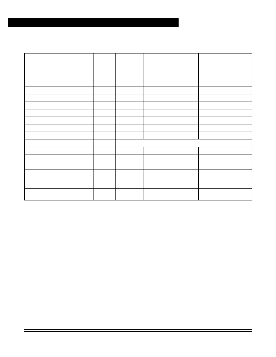
Electrical Specifications
Data Sheet
MC68HC908GR16 -- Rev. 1.0
298
Electrical Specifications
MOTOROLA
20.14 3.3-Volt ADC Characteristics
Characteristic
(1)
Symbol
Min
Max
Unit
Comments
Supply voltage
V
DDAD
3.0
3.6
V
V
DDAD
should be tied to
the same potential as V
DD
via separate traces.
Input voltages
V
ADIN
0
V
DDAD
V
V
ADIN
<= V
DDAD
Resolution
B
AD
10
10
Bits
Absolute accuracy
A
AD
�6
+6
Counts
Includes quantization
ADC internal clock
f
ADIC
500 k
1.048 M
Hz
t
AIC
= 1/f
ADIC
Conversion range
R
AD
V
SSAD
V
DDAD
V
Power-up time
t
ADPU
16
--
t
AIC
cycles
Conversion time
t
ADC
16
17
t
AIC
cycles
Sample time
t
ADS
5
--
t
AIC
cycles
Monotonicity
M
AD
Guaranteed
Zero input reading
Z
ADI
000
005
Hex
V
ADIN
= V
SSA
Full-scale reading
F
ADI
3FA
3FF
Hex
V
ADIN
= V
DDA
Input capacitance
C
ADI
--
30
pF
Not tested
V
DDAD
/V
REFH
current
I
VREF
--
1.2
mA
Absolute accuracy
(8-bit truncation mode)
A
AD
�1
+
1
LSB
Includes quantization
Quantization error
(8-bit truncation mode)
--
�1/8
+7/8
LSB
1. V
DD
= 3.3 Vdc
�
10%, V
SS
= 0 Vdc, V
DDAD/VREFH
= 3.3 Vdc
�
10%, V
SSAD
/V
REFL
= 0 Vdc
Electrical Specifications
Timer Interface Module Characteristics
MC68HC908GR16 -- Rev. 1.0
Data Sheet
MOTOROLA
Electrical Specifications
299
20.15 Timer Interface Module Characteristics
Figure 20-17. Timer Input Timing
Characteristic
Symbol
Min
(1)
Max
Unit
Timer input capture pulse width
t
TH
, t
TL
2
--
t
CYC
Timer input capture period
t
TLTL
Note 1
--
t
CYC
Timer input clock pulse width
t
TCH,
t
TCL
t
CYC
+5
--
t
CYC
1. The minimum period is the number of cycles it takes to execute the interrupt service routine plus 1 t
CYC
.
TCLK
t
TCH
t
TCL

Electrical Specifications
Data Sheet
MC68HC908GR16 -- Rev. 1.0
300
Electrical Specifications
MOTOROLA
20.16 5.0-Volt SPI Characteristics
Diagram
Number
(1)
1. Numbers refer to dimensions in
Figure 20-18
and
Figure 20-19
.
Characteristic
(2)
2. All timing is shown with respect to 20% V
DD
and 70% V
DD
, unless noted; 100 pF load on all SPI pins.
Symbol
Min
Max
Unit
Operating frequency
Master
Slave
f
OP(M)
f
OP(S)
f
OP
/128
dc
f
OP
/2
f
OP
MHz
MHz
1
Cycle time
Master
Slave
t
CYC(M)
t
CYC(S)
2
1
128
--
t
CYC
t
CYC
2
Enable lead time
t
Lead(S)
1
--
t
CYC
3
Enable lag time
t
Lag(S)
1
--
t
CYC
4
Clock (SPSCK) high time
Master
Slave
t
SCKH(M)
t
SCKH(S)
t
CYC
�25
1/2 t
CYC
�25
64 t
CYC
--
ns
ns
5
Clock (SPSCK) low time
Master
Slave
t
SCKL(M)
t
SCKL(S)
t
CYC
�25
1/2 t
CYC
�25
64 t
CYC
--
ns
ns
6
Data setup time (inputs)
Master
Slave
t
SU(M)
t
SU(S)
30
30
--
--
ns
ns
7
Data hold time (inputs)
Master
Slave
t
H(M)
t
H(S)
30
30
--
--
ns
ns
8
Access time, slave
(3)
CPHA = 0
CPHA = 1
3. Time to data active from high-impedance state
t
A(CP0)
t
A(CP1)
0
0
40
40
ns
ns
9
Disable time, slave
(4)
4. Hold time to high-impedance state
t
DIS(S)
--
40
ns
10
Data valid time, after enable edge
Master
Slave
(5)
5. With 100 pF on all SPI pins
t
V(M)
t
V(S)
--
--
50
50
ns
ns
11
Data hold time, outputs, after enable edge
Master
Slave
t
HO(M)
t
HO(S)
0
0
--
--
ns
ns

Electrical Specifications
3.3-Volt SPI Characteristics
MC68HC908GR16 -- Rev. 1.0
Data Sheet
MOTOROLA
Electrical Specifications
301
20.17 3.3-Volt SPI Characteristics
Diagram
Number
(1)
1. Numbers refer to dimensions in
Figure 20-18
and
Figure 20-19
.
Characteristic
(2)
2. All timing is shown with respect to 20% V
DD
and 70% V
DD
, unless noted; 100 pF load on all SPI pins.
Symbol
Min
Max
Unit
Operating frequency
Master
Slave
f
OP(M)
f
OP(S)
f
OP
/128
DC
f
OP
/2
f
OP
MHz
MHz
1
Cycle time
Master
Slave
t
CYC(M)
t
CYC(S)
2
1
128
--
t
cyc
t
cyc
2
Enable lead time
t
Lead(S)
1
--
t
cyc
3
Enable lag time
t
Lag(S)
1
--
t
cyc
4
Clock (SPSCK) high time
Master
Slave
t
SCKH(M)
t
SCKH(S)
t
cyc
�35
1/2 t
cyc
�35
64 t
cyc
--
ns
ns
5
Clock (SPSCK) low time
Master
Slave
t
SCKL(M)
t
SCKL(S)
t
cyc
�35
1/2 t
cyc
�35
�
64 t
cyc
--
ns
ns
6
Data setup time (inputs)
Master
Slave
t
SU(M)
t
SU(S)
40
40
--
--
ns
ns
7
Data hold time (inputs)
Master
Slave
t
H(M)
t
H(S)
40
40
--
--
ns
ns
8
Access time, slave
(3)
CPHA = 0
CPHA = 1
3. Time to data active from high-impedance state
t
A(CP0)
t
A(CP1)
0
0
50
50
ns
ns
9
Disable time, slave
(4)
4. Hold time to high-impedance state
t
DIS(S)
--
50
ns
10
Data valid time, after enable edge
Master
Slave
(5)
5. With 100 pF on all SPI pins
t
V(M)
t
V(S)
--
--
60
60
ns
ns
11
Data hold time, outputs, after enable edge
Master
Slave
t
HO(M)
t
HO(S)
0
0
--
--
ns
ns
Electrical Specifications
Data Sheet
MC68HC908GR16 -- Rev. 1.0
302
Electrical Specifications
MOTOROLA
Figure 20-18. SPI Master Timing
NOTE
Note: This first clock edge is generated internally, but is not seen at the SPSCK pin.
SS PIN OF MASTER HELD HIGH
MSB IN
SS
INPUT
SPSCK OUTPUT
SPSCK OUTPUT
MISO
INPUT
MOSI
OUTPUT
NOTE
4
5
5
1
4
BITS 6�1
LSB IN
MASTER MSB OUT
BITS 6�1
MASTER LSB OUT
11
10
11
7
6
NOTE
Note: This last clock edge is generated internally, but is not seen at the SPSCK pin.
SS PIN OF MASTER HELD HIGH
MSB IN
SS
INPUT
SPSCK OUTPUT
SPSCK OUTPUT
MISO
INPUT
MOSI
OUTPUT
NOTE
4
5
5
1
4
BITS 6�1
LSB IN
MASTER MSB OUT
BITS 6�1
MASTER LSB OUT
10
11
10
7
6
a) SPI Master Timing (CPHA = 0)
b) SPI Master Timing (CPHA = 1)
CPOL = 0
CPOL = 1
CPOL = 0
CPOL = 1
Electrical Specifications
3.3-Volt SPI Characteristics
MC68HC908GR16 -- Rev. 1.0
Data Sheet
MOTOROLA
Electrical Specifications
303
Figure 20-19. SPI Slave Timing
Note: Not defined but normally MSB of character just received
SLAVE
SS
INPUT
SPSCK INPUT
SPSCK INPUT
MISO
INPUT
MOSI
OUTPUT
4
5
5
1
4
MSB IN
BITS 6�1
8
6
10
5
11
NOTE
SLAVE LSB OUT
9
3
LSB IN
2
7
BITS 6�1
MSB OUT
Note: Not defined but normally LSB of character previously transmitted
SLAVE
SS
INPUT
SPSCK INPUT
SPSCK INPUT
MISO
OUTPUT
MOSI
INPUT
4
5
5
1
4
MSB IN
BITS 6�1
8
6
10
NOTE
SLAVE LSB OUT
9
3
LSB IN
2
7
BITS 6�1
MSB OUT
10
a) SPI Slave Timing (CPHA = 0)
b) SPI Slave Timing (CPHA = 1)
11
11
CPOL = 0
CPOL = 1
CPOL = 0
CPOL = 1
Electrical Specifications
Data Sheet
MC68HC908GR16 -- Rev. 1.0
304
Electrical Specifications
MOTOROLA
20.18 Memory Characteristics
Characteristic
Symbol
Min
Typ
Max
Unit
RAM data retention voltage
V
RDR
1.3
--
--
V
FLASH program bus clock frequency
--
1
--
--
MHz
FLASH read bus clock frequency
f
Read
(1)
1. f
Read
is defined as the frequency range for which the FLASH memory can be read.
8 k
--
8.4M
Hz
FLASH page erase time
t
Erase
(2)
2. If the page erase time is longer than t
Erase
(Min), there is no erase-disturb, but it reduces the endurance of the FLASH
memory.
1
--
--
ms
FLASH mass erase time
t
MErase
(3)
3. If the mass erase time is longer than t
MErase
(Min), there is no erase-disturb, but it reduces the endurance of the FLASH
memory.
4
--
--
ms
FLASH PGM/ERASE to HVEN set up time
t
NVS
10
--
--
�
s
FLASH high-voltage hold time
t
NVH
5
--
--
�
s
FLASH high-voltage hold time (mass erase)
t
NVHL
100
--
--
�
s
FLASH program hold time
t
PGS
5
--
--
�
s
FLASH program time
t
PROG
30
--
40
�
s
FLASH return to read time
t
RCV
(4)
4. t
RCV
is defined as the time it needs before the FLASH can be read after turning off the high voltage charge pump, by
clearing HVEN to logic 0.
1
--
--
�
s
FLASH cumulative program HV period
t
HV
(5)
5. t
HV
is defined as the cumulative high voltage programming time to the same row before next erase.
t
HV
must satisfy this condition: t
NVS
+ t
NVH
+ t
PGS
+ (t
PROG
�
64)
t
HV
max.
--
--
4
ms
FLASH row erase endurance
(6)
6. The minimum row endurance value specifies each row of the FLASH memory is guaranteed to work for at least this many
erase / program cycles.
--
10k
100k
(7)
7. FLASH endurance is a function of the temperature at which erasure occurs. Typical endurance degrades when the
temperature while erasing is less than 25
�
C.
--
Cycles
FLASH row program endurance
(8)
8. The minimum row endurance value specifies each row of the FLASH memory is guaranteed to work for at least this many
erase / program cycles.
--
10k
100k
(7)
--
Cycles
FLASH data retention time
(9)
9. The FLASH is guaranteed to retain data over the entire operating temperature range for at least the minimum time
specified.
--
10
100
(10)
10. Motorola performs reliability testing for data retention. These tests are based on samples tested at elevated temperatures.
Due to the higher activation energy of the elevated test temperature, calculated life tests correspond to more than 100
years of operation/storage at 55
�
C
--
Years
MC68HC908GR16 -- Rev. 1.0
Data Sheet
MOTOROLA
Ordering Information and Mechanical Specifications
305
Data Sheet -- MC68HC908GR16
Section 21. Ordering Information and Mechanical Specifications
21.1 Introduction
This section provides ordering information for the MC68HC908GR16 along with
the dimensions for:
�
48-pin low-profile quad flat pack (LQFP)
�
32-pin low-profile quad flat pack (LQFP)
The following figures show the latest package drawings at the time of this
publication. To make sure that you have the latest package specifications, contact
your local Motorola Sales Office.
21.2 MC Order Numbers
Figure 21-1. Device Numbering System
Table 21-1. MC Order Numbers
MC Order
Number
Operating
Temperature Range
Package
MC68HC908GR16CFJ
�40
�
C to +85
�
C
32-pin
low-profile quad package
(LQFP)
MC68HC908GR16VFJ
�40
�
C to +105
�
C
MC68HC908GR16MFJ
�40
�
C to +125
�
C
MC68HC908GR16CFA
�40
�
C to +85
�
C
48-pin
low-profile quad package
(LQFP)
MC68HC908GR16VFA
�40
�
C to +105
�
C
MC68HC908GR16MFA
�40
�
C to +125
�
C
Temperature designators:
C = �40�C to +85�C
V = �40�C to +105�C
M = �40�C to +125�C
M C 6 8 H C 9 0 8 G R 1 6 X X X
FAMILY
PACKAGE DESIGNATOR
TEMPERATURE RANGE
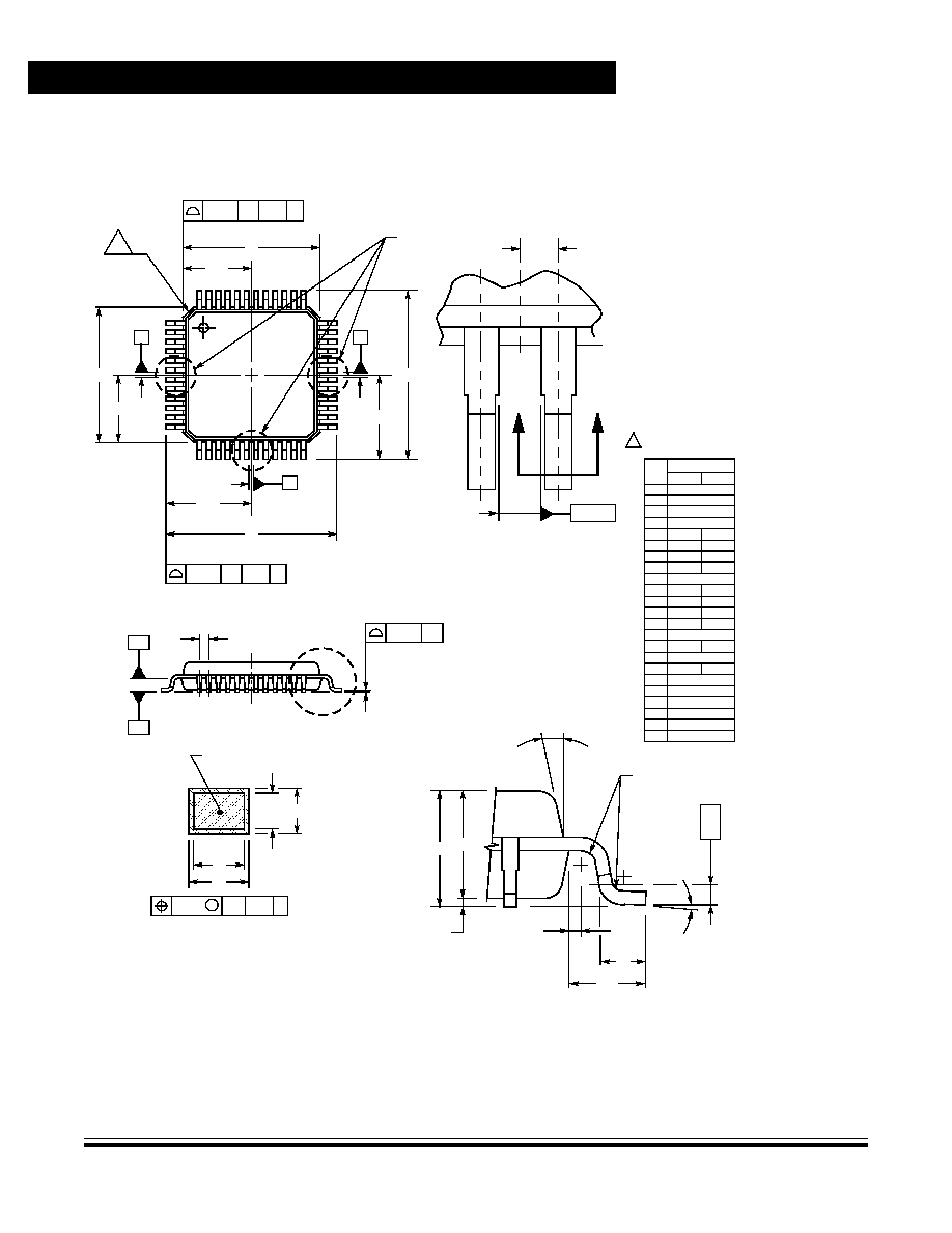
Ordering Information and Mechanical Specifications
Data Sheet
MC68HC908GR16 -- Rev. 1.0
306
Ordering Information and Mechanical Specifications
MOTOROLA
21.3 48-Pin LQFP (Case #932)
A
A1
Z
0.200 AB T-U
4X
Z
0.200 AC T-U
4X
B
B1
1
12
13
24
25
36
37
48
S1
S
V
V1
P
AE
AE
T, U, Z
DETAIL Y
DETAIL Y
BASE METAL
N
J
F
D
T-U
M
0.080
Z
AC
SECTION AE-AE
AD
G
0.080 AC
M
�
TOP & BOTTOM
L
�
W
K
AA
E
C
H
0.
250
R
9
DETAIL AD
NOTES:
1.
DIMENSIONING AND TOLERANCING PER ASME
Y14.5M, 1994.
2.
CONTROLLING DIMENSION: MILLIMETER.
3.
DATUM PLANE AB IS LOCATED AT BOTTOM OF LEAD
AND IS COINCIDENT WITH THE LEAD WHERE THE
LEAD EXITS THE PLASTIC BODY AT THE BOTTOM OF
THE PARTING LINE.
4.
DATUMS T, U, AND Z TO BE DETERMINED AT DATUM
PLANE AB.
5.
DIMENSIONS S AND V TO BE DETERMINED AT
SEATING PLANE AC.
6.
DIMENSIONS A AND B DO NOT INCLUDE MOLD
PROTRUSION. ALLOWABLE PROTRUSION IS 0.250
PER SIDE. DIMENSIONS A AND B DO INCLUDE MOLD
MISMATCH AND ARE DETERMINED AT DATUM PLANE
AB.
7.
DIMENSION D DOES NOT INCLUDE DAMBAR
PROTRUSION. DAMBAR PROTRUSION SHALL NOT
CAUSE THE D DIMENSION TO EXCEED 0.350.
8.
MINIMUM SOLDER PLATE THICKNESS SHALL BE
T
U
Z
AB
AC
G
A
UG
E PLA
N
E
DIM
A
MIN
MAX
7.000 BSC
MILLIMETERS
A1
3.500 BSC
B
7.000 BSC
B1
3.500 BSC
C
1.400
1.600
D
0.170
0.270
E
1.350
1.450
F
0.170
0.230
G
0.500 BSC
H
0.050
0.150
J
0.090
0.200
K
0.500
0.700
M
12 REF
N
0.090
0.160
P
0.250 BSC
L
0
7
R
0.150
0.250
S
9.000 BSC
S1
4.500 BSC
V
9.000 BSC
V1
4.500 BSC
W
0.200 REF
AA
1.000 REF
�
�
�
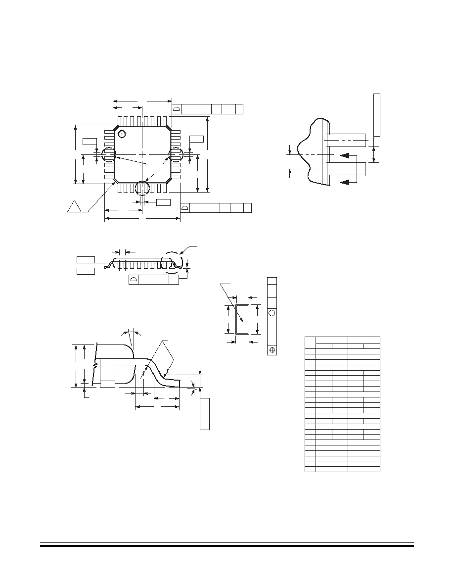
Ordering Information and Mechanical Specifications
32-Pin LQFP (Case #873A)
MC68HC908GR16 -- Rev. 1.0
Data Sheet
MOTOROLA
Ordering Information and Mechanical Specifications
307
21.4 32-Pin LQFP (Case #873A)
��
��
��
��
DETAIL Y
A
S1
V
B
1
8
9
17
25
32
AE
AE
P
DETAIL Y
BASE
N
J
D
F
METAL
SECTION AE�AE
G
SEATING
PLANE
R
Q
_
W
K
X
0.250 (0.010)
GAUGE PLANE
E
C
H
DETAIL AD
NOTES:
1. DIMENSIONING AND TOLERANCING PER ANSI
Y14.5M, 1982.
2. CONTROLLING DIMENSION: MILLIMETER.
3. DATUM PLANE �AB� IS LOCATED AT BOTTOM
OF LEAD AND IS COINCIDENT WITH THE LEAD
WHERE THE LEAD EXITS THE PLASTIC BODY AT
THE BOTTOM OF THE PARTING LINE.
4. DATUMS �T�, �U�, AND �Z� TO BE DETERMINED
AT DATUM PLANE �AB�.
5. DIMENSIONS S AND V TO BE DETERMINED AT
SEATING PLANE �AC�.
6. DIMENSIONS A AND B DO NOT INCLUDE MOLD
PROTRUSION. ALLOWABLE PROTRUSION IS
0.250 (0.010) PER SIDE. DIMENSIONS A AND B
DO INCLUDE MOLD MISMATCH AND ARE
DETERMINED AT DATUM PLANE �AB�.
7. DIMENSION D DOES NOT INCLUDE DAMBAR
PROTRUSION. DAMBAR PROTRUSION SHALL
NOT CAUSE THE D DIMENSION TO EXCEED
0.520 (0.020).
8. MINIMUM SOLDER PLATE THICKNESS SHALL BE
0.0076 (0.0003).
9. EXACT SHAPE OF EACH CORNER MAY VARY
FROM DEPICTION.
DIM
A
MIN
MAX
MIN
MAX
INCHES
7.000 BSC
0.276 BSC
MILLIMETERS
B
7.000 BSC
0.276 BSC
C
1.400
1.600
0.055
0.063
D
0.300
0.450
0.012
0.018
E
1.350
1.450
0.053
0.057
F
0.300
0.400
0.012
0.016
G
0.800 BSC
0.031 BSC
H
0.050
0.150
0.002
0.006
J
0.090
0.200
0.004
0.008
K
0.500
0.700
0.020
0.028
M
12 REF
12 REF
N
0.090
0.160
0.004
0.006
P
0.400 BSC
0.016 BSC
Q
1
5
1
5
R
0.150
0.250
0.006
0.010
V
9.000 BSC
0.354 BSC
V1
4.500 BSC
0.177 BSC
_
_
_
_
_
_
DETAIL AD
A1
B1
V1
4X
S
4X
B1
3.500 BSC
0.138 BSC
A1
3.500 BSC
0.138 BSC
S
9.000 BSC
0.354 BSC
S1
4.500 BSC
0.177 BSC
W
0.200 REF
0.008 REF
X
1.000 REF
0.039 REF
9
�T�
�Z�
�U�
T�U
0.20 (0.008)
Z
AC
T�U
0.20 (0.008)
Z
AB
0.10 (0.004) AC
�AC�
�AB�
M
_
8X
�T�, �U�, �Z�
T�U
M
0.20 (0.008)
Z
AC

Ordering Information and Mechanical Specifications
Data Sheet
MC68HC908GR16 -- Rev. 1.0
308
Ordering Information and Mechanical Specifications
MOTOROLA


HOW TO REACH US:
USA/EUROPE/LOCATIONS NOT LISTED:
Motorola Literature Distribution
P.O. Box 5405
Denver, Colorado 80217
1-800-521-6274 or 480-768-2130
JAPAN:
Motorola Japan Ltd.
SPS, Technical Information Center
3-20-1, Minami-Azabu, Minato-ku
Tokyo 106-8573, Japan
81-3-3440-3569
ASIA/PACIFIC:
Motorola Semiconductors H.K. Ltd.
Silicon Harbour Centre
2 Dai King Street
Tai Po Industrial Estate
Tai Po, N.T., Hong Kong
852-26668334
HOME PAGE:
http://motorola.com/semiconductors
MC68HC908GR16/D
Rev. 1
5/2003
Information in this document is provided solely to enable system and software implementers to use Motorola products.
There are no express or implied copyright licenses granted hereunder to design or fabricate any integrated circuits or
integrated circuits based on the information in this document.
Motorola reserves the right to make changes without further notice to any products herein. Motorola makes no warranty,
representation or guarantee regarding the suitability of its products for any particular purpose, nor does Motorola assume
any liability arising out of the application or use of any product or circuit, and specifically disclaims any and all liability,
including without limitation consequential or incidental damages. "Typical" parameters that may be provided in Motorola
data sheets and/or specifications can and do vary in different applications and actual performance may vary over time. All
operating parameters, including "Typicals", must be validated for each customer application by customer's technical experts.
Motorola does not convey any license under its patent rights nor the rights of others. Motorola products are not designed,
intended, or authorized for use as components in systems intended for surgical implant into the body, or other applications
intended to support or sustain life, or for any other application in which the failure of the Motorola product could create a
situation where personal injury or death may occur. Should Buyer purchase or use Motorola products for any such
unintended or unauthorized application, Buyer shall indemnify and hold Motorola and its officers, employees, subsidiaries,
affiliates, and distributors harmless against all claims, costs, damages, and expenses, and reasonable attorney fees arising
out of, directly or indirectly, any claim of personal injury or death associated with such unintended or unauthorized use, even
if such claim alleges that Motorola was negligent regarding the design or manufacture of the part.
MOTOROLA and the Stylized M Logo are registered in the US Patent and Trademark Office. All other product or service
names are the property of their respective owners. Motorola, Inc. is an Equal Opportunity/Affirmative Action Employer.
� Motorola Inc. 2003
Document Outline
