
© Motorola, Inc., 2003
HC908JL8AD/D
Rev. 0, 5/2002
Addendum to
MC68HC908JL8
Technical Data
Addendum
This addendum provides update and additional information to the
MC68HC908JL8 Technical Data, Rev. 2
(Motorola document number MC68HC908JL8/D)
MC68HC08JL8
MC68HC08JK8
The MC68HC08JL8 is the ROM part equivalent to the MC68HC908JL8. The
entire MC68HC908JL8 data book apply to this ROM device, with exceptions
outlined in this addendum.
Table 1. Summary of MC68HC08JL8 and MC68HC908JL8 Differences
MC68HC08JL8
MC68HC908JL8
Memory ($DC00≠$FBFF)
8,192 bytes ROM
8,192 bytes FLASH
User vectors ($FFDC≠$FFFF)
36 bytes ROM
36 bytes FLASH
Registers at $FE08 and $FFCF
Not used;
locations are reserved.
FLASH related registers.
$FE08 -- FLCR
$FFCF -- FLBPR
Mask option register ($FFD0)
Defined by mask; read only.
Read/write FLASH register.
Monitor ROM
($FC00≠$FDFF and $FE10≠$FFCE)
$FC00≠$FDFF: Not used.
$FE10≠$FFCE: Used for
testing purposes only.
Used for testing and FLASH
programming/erasing.
Available Packages
20-pin PDIP (MC68HC08JK8)
20-pin SOIC (MC68HC08JK8)
28-pin PDIP
28-pin SOIC
32-pin SDIP
32-pin LQFP
20-pin PDIP (MC68HC908JK8)
20-pin SOIC (MC68HC908JK8)
28-pin PDIP
28-pin SOIC
32-pin SDIP
32-pin LQFP
HC908JL8AD/D
2
Addendum to MC68HC908JL8 Technical Data
MOTOROLA
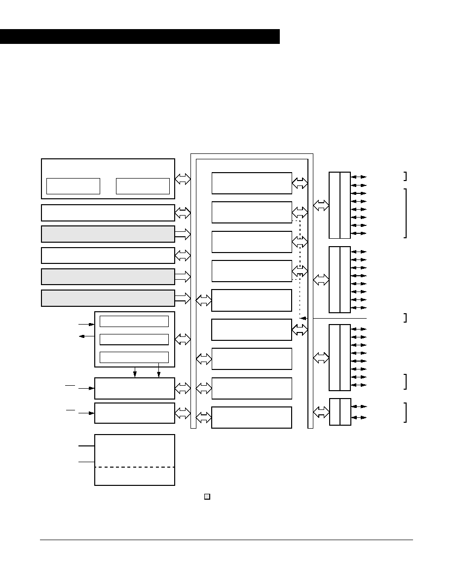
MCU Block Diagram
Figure 1
shows the block diagram of the MC68HC08JL8.
Memory Map
The MC68HC08JL8 has 8,192 bytes of user ROM from $DC00 to $FBFF, and
36 bytes of user ROM vectors from $FFDC to $FFFF. On the MC68HC908JL8,
these memory locations are FLASH memory.
Figure 2
shows the memory map of the MC68HC08JL8.
Figure 1. MC68HC08JL8 Block Diagram
SYSTEM INTEGRATION
MODULE
ARITHMETIC/LOGIC
UNIT (ALU)
CPU
REGISTERS
M68HC08 CPU
CONTROL AND STATUS REGISTERS -- 64 BYTES
EXTERNAL INTERRUPT
MODULE
INTERNAL BUS
* RST
* IRQ
POWER
VSS
2-CHANNEL TIMER INTERFACE
MODULE 1
KEYBOARD INTERRUPT
MODULE
8-BIT ANALOG-TO-DIGITAL
CONVERTER MODULE
VDD
ADC REFERENCE
DD
RB
PO
RT
B
PTB7/ADC7
PTB6/ADC6
PTB5/ADC5
PTB4/ADC4
PTB3/ADC3
PTB2/ADC2
PTB1/ADC1
PTB0/ADC0
DDR
A
PO
RT
A
PTA6/KBI6**
•
PTA5/KBI5**
PTA4/KBI4**
PTA3/KBI3**
PTA2/KBI2**
PTA1/KBI1**
PTA0/KBI0**
POWER-ON RESET
MODULE
* Pin contains integrated pull-up device.
** Pin contains programmable pull-up device.
LED direct sink pin.
OSC1
•
OSC2/RCCLK
CRYSTAL OSCILLATOR
RC OSCILLATOR
DD
RD
PO
RT
D
PTD7/RxD**
PTD6/TxD**
PTD5/T1CH1
PTD4/T1CH0
PTD3/ADC8
PTD2/ADC9
PTD1/ADC10
PTD0/ADC11
BREAK
MODULE
COMPUTER OPERATING
PROPERLY MODULE
# Pins available on 32-pin packages only.
• Shared pin: OSC2/RCCLK/PTA6/KBI6.
PTA7/KBI7**
LOW-VOLTAGE INHIBIT
MODULE
SERIAL COMMUNICATIONS
INTERFACE MODULE
PT
E
DD
RE
PTE1/T2CH1
PTE0/T2CH0
INTERNAL OSCILLATOR
ADC12/T2CLK
2-CHANNEL TIMER INTERFACE
MODULE 2
USER RAM -- 256 BYTES
MONITOR ROM -- 447 BYTES
#
##
#
##
#
## Pins available on 28-pin and 32-pin packages only.
25mA open-drain if output pin.
USER ROM -- 8,192 BYTES
USER ROM VECTORS -- 36 BYTES
Shaded blocks indicate differences to MC68HC908JL8

HC908JL8AD/D
MC68HC08JL8 MC68HC08JK8
MOTOROLA
Addendum to MC68HC908JL8 Technical Data
3
$0000
$003F
I/O REGISTERS
64 BYTES
$0040
$005F
RESERVED
32 BYTES
$0060
$015F
RAM
256 BYTES
$0160
$DBFF
UNIMPLEMENTED
55,968 BYTES
$DC00
$FBFF
ROM
8,192 BYTES
$FC00
$FDFF
UNIMPLEMENTED
512 BYTES
$FE00
BREAK STATUS REGISTER (BSR)
$FE01
RESET STATUS REGISTER (RSR)
$FE02
RESERVED
$FE03
BREAK FLAG CONTROL REGISTER (BFCR)
$FE04
INTERRUPT STATUS REGISTER 1 (INT1)
$FE05
INTERRUPT STATUS REGISTER 2 (INT2)
$FE06
INTERRUPT STATUS REGISTER 3 (INT3)
$FE07
RESERVED
$FE08
RESERVED
$FE09
$FF0B
RESERVED
$FE0C
BREAK ADDRESS HIGH REGISTER (BRKH)
$FE0D
BREAK ADDRESS LOW REGISTER (BRKL)
$FE0E
BREAK STATUS AND CONTROL REGISTER (BRKSCR)
$FE0F
RESERVED
$FE10
$FFCE
MONITOR ROM
447 BYTES
$FFCF
RESERVED
$FFD0
MASK OPTION REGISTER (MOR) -- READ ONLY
$FFD1
$FFDB
RESERVED
11 BYTES
$FFDC
$FFFF
USER ROM VECTORS
36 BYTES
Figure 2. MC68HC08JL8 Memory Map

HC908JL8AD/D
4
Addendum to MC68HC908JL8 Technical Data
MOTOROLA
Reserved Registers
The two registers at $FE08 and $FFCF are reserved locations on the
MC68HC08JL8.
On the MC68HC908JL8, these two locations are the FLASH control register
and the FLASH block protect register respectively.
Mask Option
Register
The mask option register at $FFD0 is read only. The value is defined by mask
option (hard-wired connections) specified at the time as the ROM code
submission.
On the MC68HC908JL8, the MOR is implemented as a FLASH, which can be
programmed, erased, and read.
Monitor ROM
The monitor program (monitor ROM: $FE10≠$FFCE) on the MC68HC08JL8 is
for device testing only. $FC00≠$FDFF are unused.
Electrical
Specifications
Electrical specifications for the MC68HC908JL8 apply to the MC68HC08JL8,
except for the parameters indicated below.
DC Electrical
Characteristics
Table 2. DC Electrical Characteristics (5V)
Characteristic
(1)
Symbol
Min
Typ
(2)
Max
Unit
V
DD
supply current, f
OP
= 8 MHz
RC oscillator option
I
DD
Values same as, and characterized from
MC68HC908JL8, but not tested.
Low-voltage inhibit, trip falling voltage
V
TRIPF
3.55 (3.60)
(3)
4.02 (4.25)
4.48 (4.48)
V
Low-voltage inhibit, trip rising voltage
V
TRIPR
3.66 (3.75)
4.13 (4.40)
4.59 (4.63)
V
1. V
DD
= 4.5 to 5.5 Vdc, V
SS
= 0 Vdc, T
A
= T
L
to T
H
, unless otherwise noted.
2. Typical values reflect average measurements at midpoint of voltage range, 25
∞C only.
3. The numbers in parenthesis are MC68HC908JL8 values.
Table 3. DC Electrical Characteristics (3V)
Characteristic
(1)
Symbol
Min
Typ
(2)
Max
Unit
V
DD
supply current, f
OP
= 4 MHz
RC oscillator option
I
DD
Values same as, and characterized from
MC68HC908JL8, but not tested.
Low-voltage inhibit, trip voltage
(No hysteresis implemented for 3V LVI)
V
LVI3
2.1 (2.18)
(3)
2.4 (2.49)
2.69 (2.68)
V
1. V
DD
= 2.7 to 3.3 Vdc, V
SS
= 0 Vdc, T
A
= T
L
to T
H
, unless otherwise noted.
2. Typical values reflect average measurements at midpoint of voltage range, 25
∞C only.
3. The numbers in parenthesis are MC68HC908JL8 values.
HC908JL8AD/D
MC68HC08JL8 MC68HC08JK8
MOTOROLA
Addendum to MC68HC908JL8 Technical Data
5
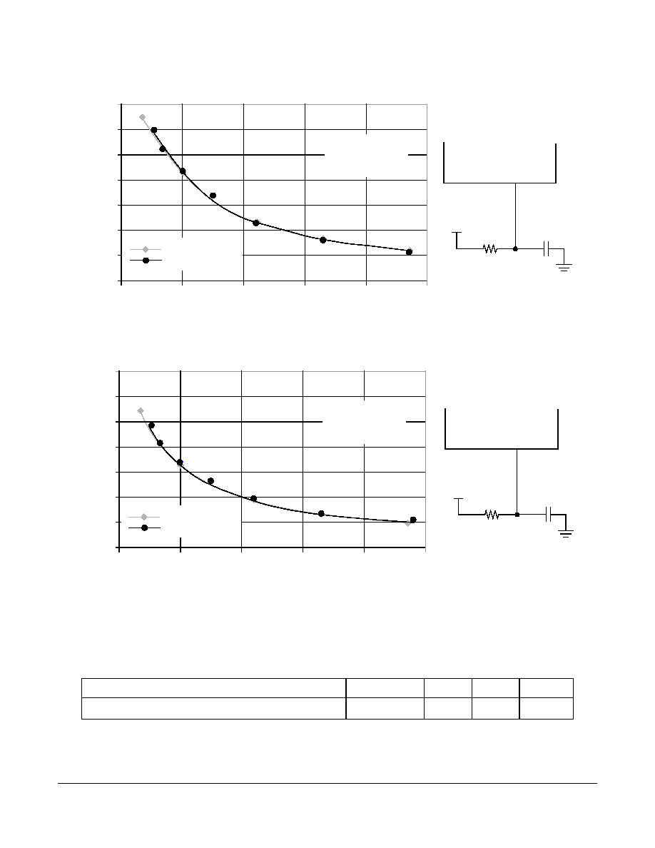
Figure 3. RC vs. Frequency (5V @25
∞C)
Figure 4. RC vs. Frequency (3V @25
∞C)
Memory
Characteristics
R
EXT
C
EXT
OSC1
V
DD
MCU
0
0
10
20
30
40
50
14
12
10
8
6
4
2
Resistor, R
EXT
(k
)
RC f
r
e
que
nc
y
,
f
RC
CLK
(M
Hz
)
C
EXT
= 10 pF
5V @ 25
∞C
MC68HC908JL8
MC68HC08JL8
R
EXT
C
EXT
OSC1
V
DD
MCU
0
0
10
20
30
40
50
14
12
10
8
6
4
2
Resistor, R
EXT
(k
)
RC fr
eq
uen
cy
, f
RCCLK
(M
Hz)
C
EXT
= 10 pF
3V @ 25
∞C
MC68HC908JL8
MC68HC08JL8
Table 4. Memory Characteristics
Characteristic
Symbol
Min
Max
Unit
RAM data retention voltage
V
RDR
1.3
--
V
Notes:
Since MC68HC08JL8 is a ROM device, FLASH memory electrical characteristics do not apply.

HC908JL8AD/D
6
Addendum to MC68HC908JL8 Technical Data
MOTOROLA
MC68HC08JL8
Order Numbers
These part numbers are generic numbers only. To place an order, ROM code
must be submitted to the ROM Processing Center (RPC).
Table 5. MC68HC08JL8 Order Numbers
MC Order Number
Operating
Temperature Range
Package
MC68HC08JK8CP
≠40
∞C to +85 ∞C
20-pin PDIP
MC68HC08JK8MP
≠40
∞C to +125 ∞C
MC68HC08JK8CDW
≠40
∞C to +85 ∞C
20-pin SOIC
MC68HC08JK8MDW
≠40
∞C to +125 ∞C
MC68HC08JL8CP
≠40
∞C to +85 ∞C
28-pin PDIP
MC68HC08JL8MP
≠40
∞C to +125 ∞C
MC68HC08JL8CDW
≠40
∞C to +85 ∞C
28-pin SOIC
MC68HC08JL8MDW
≠40
∞C to +125 ∞C
MC68HC08JL8CSP
≠40
∞C to +85 ∞C
32-pin SDIP
MC68HC08JL8MSP
≠40
∞C to +125 ∞C
MC68HC08JL8CFA
≠40
∞C to +85 ∞C
32-pin LQFP
MC68HC08JL8MFA
≠40
∞C to +125 ∞C
NOTE: Temperature grade "M" is available for V
DD
= 5V only.

HC908JL8AD/D
AMENDMENTS TO MC68HC908JL8/D, REV. 2
MOTOROLA
Addendum to MC68HC908JL8 Technical Data
7
AMENDMENTS TO MC68HC908JL8/D, REV. 2
Keyboard Interrupt
Page 243, Figure 15-2. Keyboard Interrupt Block Diagram -- Replace with
the following block diagram:
Computer Operating
Properly (COP)
Page 254, 16.8.2 Stop Mode -- Replace the two paragraphs:
From:
Stop mode turns off the ICLK input to the COP if the STOP_ICLKDIS bit is set
in configuration register 2 (CONFIG2). Service the COP immediately before
entering or after exiting stop mode to ensure a full COP timeout period after
entering or exiting stop mode.
After reset, the STOP_ICLKDIS bit is clear by default and ICLK is enabled
during stop mode.
To:
Stop mode turns off the ICLK input to the COP and clears the COP prescaler.
Service the COP immediately before entering or after exiting stop mode to
ensure a full COP timeout period after entering or exiting stop mode.
To prevent inadvertently turning off the COP with a STOP instruction, a
configuration option is available that disables the STOP instruction. When the
STOP bit in the configuration register has the STOP instruction is disabled,
execution of a STOP instruction results in an illegal opcode reset.
KBIE0
KBIE7
.
.
.
D
Q
CK
CLR
V
DD
MODEK
IMASKK
KEYBOARD
INTERRUPT FF
VECTOR FETCH
DECODER
ACKK
INTERNAL BUS
RESET
KBI7
KBI0
SYNCHRONIZER
KEYF
KEYBOARD
INTERRUPT
REQUEST
TO PULLUP ENABLE
TO PULLUP ENABLE
NOTE:
To prevent false interrupts, user should use software
to debounce keyboard interrupt inputs.

Information in this document is provided solely to enable system and software
implementers to use Motorola products. There are no express or implied copyright
licenses granted hereunder to design or fabricate any integrated circuits or
integrated circuits based on the information in this document.
Motorola reserves the right to make changes without further notice to any products
herein. Motorola makes no warranty, representation or guarantee regarding the
suitability of its products for any particular purpose, nor does Motorola assume any
liability arising out of the application or use of any product or circuit, and specifically
disclaims any and all liability, including without limitation consequential or incidental
damages. "Typical" parameters which may be provided in Motorola data sheets
and/or specifications can and do vary in different applications and actual
performance may vary over time. All operating parameters, including "Typicals"
must be validated for each customer application by customer's technical experts.
Motorola does not convey any license under its patent rights nor the rights of
others. Motorola products are not designed, intended, or authorized for use as
components in systems intended for surgical implant into the body, or other
applications intended to support or sustain life, or for any other application in which
the failure of the Motorola product could create a situation where personal injury or
death may occur. Should Buyer purchase or use Motorola products for any such
unintended or unauthorized application, Buyer shall indemnify and hold Motorola
and its officers, employees, subsidiaries, affiliates, and distributors harmless
against all claims, costs, damages, and expenses, and reasonable attorney fees
arising out of, directly or indirectly, any claim of personal injury or death associated
with such unintended or unauthorized use, even if such claim alleges that Motorola
was negligent regarding the design or manufacture of the part.
Motorola and the Stylized M Logo are registered in the U.S. Patent and Trademark
Office. digital dna is a trademark of Motorola, Inc. All other product or service
names are the property of their respective owners. Motorola, Inc. is an Equal
Opportunity/Affirmative Action Employer.
© Motorola, Inc. 2003
HC908JL8AD/D
Rev. 0
5/2003
HOW TO REACH US:
USA/EUROPE/LOCATIONS NOT LISTED:
Motorola Literature Distribution
P.O. Box 5405, Denver, Colorado 80217
1-800-521-6274 or 480-768-2130
JAPAN:
Motorola Japan Ltd.; SPS, Technical Information Center
3-20-1, Minami-Azabu Minato-ku, Tokyo 106-8573 Japan
81-3-3440-3569
ASIA/PACIFIC:
Motorola Semiconductors H.K. Ltd.
Silicon Harbour Centre, 2 Dai King Street
Tai Po Industrial Estate, Tai Po, N.T., Hong Kong
852-26668334
HOME PAGE:
http://motorola.com/semiconductors