
Motorola reserves the right to make changes without further notice to any products herein to improve reliability, function or
design. Motorola does not assume any liability arising out of the application or use of any product or circuit described herein;
neither does it convey any license under its patent rights nor the rights of others. Motorola products are not designed, intended,
or authorized for use as components in systems intended for surgical implant into the body, or other applications intended to
support or sustain life, or for any other application in which the failure of the Motorola product could create a situation where
personal injury or death may occur. Should Buyer purchase or use Motorola products for any such unintended or unauthorized
application, Buyer shall indemnify and hold Motorola and its officers, employees, subsidiaries, affiliates, and distributors harmless
against all claims, costs, damages, and expenses, and reasonable attorney fees arising out of, directly or indirectly, any claim of
personal injury or death associated with such unintended or unauthorized use, even if such claim alleges that Motorola was
negligent regarding the design or manufacture of the part.
9S12A128DGV1/D
4/2002
1
MC9S12A128
Device Guide
V01.01
Original Release Date: 8 March, 2002
Revised: 17 April, 2002
Motorola, Inc
MC9S12A128 Device Guide -- V01.01
2
Revision History
For additional information, refer to the MC9S12A128 8-Bit Microcontroller Unit Mask Set Errata
(Motorola document order number, 9S12A128MSE1). The errata can be found on the World Wide Web at:
http://www.motorola.com/semiconductors/
Version
Number
Revision
Date
Effective
Date
Author
Description of Changes
V01.00
8 MAR
2002
8 MAR
2002
Initial release
V01.01
17 APRIL
2002
12 APRIL
2002
Replaced document order number with version except for cover
sheet
Corrected
Table 1-1 Device Memory Map
entries for EEPROM
array and RAM array
Table A-4 Operating Conditions
-- Increased V
DD
to 2.35V
Table A-6 5V I/O Characteristics
-- Corrected rating column for
V
OH
and V
OL
and typical value for C
in
Table A-8 ATD Operating Characteristics
-- Updated rating
definitions for items 6, 7, and 8 for clarity

MC9S12A128 Device Guide -- V01.01
3
Table of Contents
Section 1 Introduction
1.1
Overview. . . . . . . . . . . . . . . . . . . . . . . . . . . . . . . . . . . . . . . . . . . . . . . . . . . . . . . . . . . . . 15
1.2
Features . . . . . . . . . . . . . . . . . . . . . . . . . . . . . . . . . . . . . . . . . . . . . . . . . . . . . . . . . . . . . 15
1.3
Modes of Operation . . . . . . . . . . . . . . . . . . . . . . . . . . . . . . . . . . . . . . . . . . . . . . . . . . . .17
1.4
Block Diagram . . . . . . . . . . . . . . . . . . . . . . . . . . . . . . . . . . . . . . . . . . . . . . . . . . . . . . . . 18
1.5
Device Memory Map. . . . . . . . . . . . . . . . . . . . . . . . . . . . . . . . . . . . . . . . . . . . . . . . . . . .20
1.6
Part ID Assignments. . . . . . . . . . . . . . . . . . . . . . . . . . . . . . . . . . . . . . . . . . . . . . . . . . . .22
Section 2 Signal Description
2.1
Device Pinout . . . . . . . . . . . . . . . . . . . . . . . . . . . . . . . . . . . . . . . . . . . . . . . . . . . . . . . . .23
2.2
Signal Properties Summary . . . . . . . . . . . . . . . . . . . . . . . . . . . . . . . . . . . . . . . . . . . . . . 26
2.3
Detailed Signal Descriptions. . . . . . . . . . . . . . . . . . . . . . . . . . . . . . . . . . . . . . . . . . . . . . 28
2.3.1
EXTAL, XTAL -- Oscillator Pins . . . . . . . . . . . . . . . . . . . . . . . . . . . . . . . . . . . . . . . . 28
2.3.2
RESET -- External Reset Pin . . . . . . . . . . . . . . . . . . . . . . . . . . . . . . . . . . . . . . . . . . 28
2.3.3
TEST -- Test Pin . . . . . . . . . . . . . . . . . . . . . . . . . . . . . . . . . . . . . . . . . . . . . . . . . . . .28
2.3.4
V
REGEN
-- Voltage Regulator Enable Pin . . . . . . . . . . . . . . . . . . . . . . . . . . . . . . . . .28
2.3.5
XFC -- PLL Loop Filter Pin . . . . . . . . . . . . . . . . . . . . . . . . . . . . . . . . . . . . . . . . . . . . 28
2.3.6
BKGD / TAGHI / MODC -- Background Debug, Tag High, and Mode Pin . . . . . . . . 29
2.3.7
PAD15 / AN15 / ETRIG1 -- Port AD Input Pin of ATD1 . . . . . . . . . . . . . . . . . . . . . . 29
2.3.8
PAD[14:08] / AN[14:08] -- Port AD Input Pins of ATD1 . . . . . . . . . . . . . . . . . . . . . . 29
2.3.9
PAD7 / AN07 / ETRIG0 -- Port AD Input Pin of ATD0 . . . . . . . . . . . . . . . . . . . . . . . 29
2.3.10
PAD[06:00] / AN[06:00] -- Port AD Input Pins of ATD0 . . . . . . . . . . . . . . . . . . . . . . 29
2.3.11
PA[7:0] / ADDR[15:8] / DATA[15:8] -- Port A I/O Pins . . . . . . . . . . . . . . . . . . . . . . . 29
2.3.12
PB[7:0] / ADDR[7:0] / DATA[7:0] -- Port B I/O Pins . . . . . . . . . . . . . . . . . . . . . . . . . 29
2.3.13
PE7 / NOACC / XCLKS -- Port E I/O Pin 7 . . . . . . . . . . . . . . . . . . . . . . . . . . . . . . . . 29
2.3.14
PE6 / MODB / IPIPE1 -- Port E I/O Pin 6 . . . . . . . . . . . . . . . . . . . . . . . . . . . . . . . . .30
2.3.15
PE5 / MODA / IPIPE0 -- Port E I/O Pin 5 . . . . . . . . . . . . . . . . . . . . . . . . . . . . . . . . .30
2.3.16
PE4 / ECLK -- Port E I/O Pin 4 . . . . . . . . . . . . . . . . . . . . . . . . . . . . . . . . . . . . . . . . . 30
2.3.17
PE3 / LSTRB / TAGLO -- Port E I/O Pin 3 . . . . . . . . . . . . . . . . . . . . . . . . . . . . . . . . 30
2.3.18
PE2 / R/W -- Port E I/O Pin 2 . . . . . . . . . . . . . . . . . . . . . . . . . . . . . . . . . . . . . . . . . . 30
2.3.19
PE1 / IRQ -- Port E Input Pin 1 . . . . . . . . . . . . . . . . . . . . . . . . . . . . . . . . . . . . . . . . . 30
2.3.20
PE0 / XIRQ -- Port E Input Pin 0. . . . . . . . . . . . . . . . . . . . . . . . . . . . . . . . . . . . . . . . 30
2.3.21
PH7 / KWH7 -- Port H I/O Pin 7 . . . . . . . . . . . . . . . . . . . . . . . . . . . . . . . . . . . . . . . . 31

MC9S12A128 Device Guide -- V01.01
4
2.3.22
PH6 / KWH6 -- Port H I/O Pin 6 . . . . . . . . . . . . . . . . . . . . . . . . . . . . . . . . . . . . . . . . 31
2.3.23
PH5 / KWH5 -- Port H I/O Pin 5 . . . . . . . . . . . . . . . . . . . . . . . . . . . . . . . . . . . . . . . . 31
2.3.24
PH4 / KWH4 -- Port H I/O Pin 4 . . . . . . . . . . . . . . . . . . . . . . . . . . . . . . . . . . . . . . . . 31
2.3.25
PH3 / KWH3 / SS1 -- Port H I/O Pin 3 . . . . . . . . . . . . . . . . . . . . . . . . . . . . . . . . . . . 31
2.3.26
PH2 / KWH2 / SCK1 -- Port H I/O Pin 2 . . . . . . . . . . . . . . . . . . . . . . . . . . . . . . . . . . 31
2.3.27
PH1 / KWH1 / MOSI1 -- Port H I/O Pin 1 . . . . . . . . . . . . . . . . . . . . . . . . . . . . . . . . .31
2.3.28
PH0 / KWH0 / MISO1 -- Port H I/O Pin 0 . . . . . . . . . . . . . . . . . . . . . . . . . . . . . . . . .31
2.3.29
PJ7 / KWJ7 / SCL -- PORT J I/O Pin 7 . . . . . . . . . . . . . . . . . . . . . . . . . . . . . . . . . . . 32
2.3.30
PJ6 / KWJ6 / SDA -- PORT J I/O Pin 6. . . . . . . . . . . . . . . . . . . . . . . . . . . . . . . . . . . 32
2.3.31
PJ[1:0] / KWJ[1:0] -- Port J I/O Pins [1:0] . . . . . . . . . . . . . . . . . . . . . . . . . . . . . . . . .32
2.3.32
PK7 / ECS / ROMON -- Port K I/O Pin 7. . . . . . . . . . . . . . . . . . . . . . . . . . . . . . . . . .32
2.3.33
PK[5:0] / XADDR[19:14] -- Port K I/O Pins [5:0] . . . . . . . . . . . . . . . . . . . . . . . . . . . . 32
2.3.34
PM7 -- Port M I/O Pin 7. . . . . . . . . . . . . . . . . . . . . . . . . . . . . . . . . . . . . . . . . . . . . . . 32
2.3.35
PM6 -- Port M I/O Pin 6. . . . . . . . . . . . . . . . . . . . . . . . . . . . . . . . . . . . . . . . . . . . . . . 32
2.3.36
PM5 / SCK0 -- Port M I/O Pin 5 . . . . . . . . . . . . . . . . . . . . . . . . . . . . . . . . . . . . . . . . 32
2.3.37
PM4 / MOSI0 -- Port M I/O Pin 4 . . . . . . . . . . . . . . . . . . . . . . . . . . . . . . . . . . . . . . . 32
2.3.38
PM3 / SS0 -- Port M I/O Pin 3. . . . . . . . . . . . . . . . . . . . . . . . . . . . . . . . . . . . . . . . . . 33
2.3.39
PM2 / MISO0 -- Port M I/O Pin 2 . . . . . . . . . . . . . . . . . . . . . . . . . . . . . . . . . . . . . . . 33
2.3.40
PM1 -- Port M I/O Pin 1. . . . . . . . . . . . . . . . . . . . . . . . . . . . . . . . . . . . . . . . . . . . . . . 33
2.3.41
PM0 -- Port M I/O Pin 0. . . . . . . . . . . . . . . . . . . . . . . . . . . . . . . . . . . . . . . . . . . . . . . 33
2.3.42
PP7 / KWP7 / PWM7 -- Port P I/O Pin 7 . . . . . . . . . . . . . . . . . . . . . . . . . . . . . . . . . .33
2.3.43
PP6 / KWP6 / PWM6 -- Port P I/O Pin 6 . . . . . . . . . . . . . . . . . . . . . . . . . . . . . . . . . .33
2.3.44
PP5 / KWP5 / PWM5 -- Port P I/O Pin 5 . . . . . . . . . . . . . . . . . . . . . . . . . . . . . . . . . .33
2.3.45
PP4 / KWP4 / PWM4 -- Port P I/O Pin 4 . . . . . . . . . . . . . . . . . . . . . . . . . . . . . . . . . .33
2.3.46
PP3 / KWP3 / PWM3 / SS1 -- Port P I/O Pin 3 . . . . . . . . . . . . . . . . . . . . . . . . . . . . .33
2.3.47
PP2 / KWP2 / PWM2 / SCK1 -- Port P I/O Pin 2 . . . . . . . . . . . . . . . . . . . . . . . . . . . 34
2.3.48
PP1 / KWP1 / PWM1 / MOSI1 -- Port P I/O Pin 1. . . . . . . . . . . . . . . . . . . . . . . . . . . 34
2.3.49
PP0 / KWP0 / PWM0 / MISO1 -- Port P I/O Pin 0. . . . . . . . . . . . . . . . . . . . . . . . . . . 34
2.3.50
PS7 / SS0 -- Port S I/O Pin 7 . . . . . . . . . . . . . . . . . . . . . . . . . . . . . . . . . . . . . . . . . . 34
2.3.51
PS6 / SCK0 -- Port S I/O Pin 6 . . . . . . . . . . . . . . . . . . . . . . . . . . . . . . . . . . . . . . . . . 34
2.3.52
PS5 / MOSI0 -- Port S I/O Pin 5 . . . . . . . . . . . . . . . . . . . . . . . . . . . . . . . . . . . . . . . . 34
2.3.53
PS4 / MISO0 -- Port S I/O Pin 4 . . . . . . . . . . . . . . . . . . . . . . . . . . . . . . . . . . . . . . . . 34
2.3.54
PS3 / TXD1 -- Port S I/O Pin 3 . . . . . . . . . . . . . . . . . . . . . . . . . . . . . . . . . . . . . . . . . 34
2.3.55
PS2 / RXD1 -- Port S I/O Pin 2 . . . . . . . . . . . . . . . . . . . . . . . . . . . . . . . . . . . . . . . . . 35
2.3.56
PS1 / TXD0 -- Port S I/O Pin 1 . . . . . . . . . . . . . . . . . . . . . . . . . . . . . . . . . . . . . . . . . 35
2.3.57
PS0 / RXD0 -- Port S I/O Pin 0 . . . . . . . . . . . . . . . . . . . . . . . . . . . . . . . . . . . . . . . . . 35

MC9S12A128 Device Guide -- V01.01
5
2.3.58
PT[7:0] / IOC[7:0] -- Port T I/O Pins [7:0] . . . . . . . . . . . . . . . . . . . . . . . . . . . . . . . . .35
2.4
Power Supply Pins . . . . . . . . . . . . . . . . . . . . . . . . . . . . . . . . . . . . . . . . . . . . . . . . . . . . . 35
2.4.1
V
DDX
, V
SSX
-- Power & Ground Pins for I/O Drivers . . . . . . . . . . . . . . . . . . . . . . . . . 35
2.4.2
V
DDR
, V
SSR
-- Power & Ground Pins for I/O
Drivers & for Internal Voltage Regulator . . . . . . . . . . . . . . . . . . . . . . . . . . . . . . . . 35
2.4.3
V
DD1
, V
DD2
, V
SS1
, V
SS2
-- Core Power Pins. . . . . . . . . . . . . . . . . . . . . . . . . . . . . . . 36
2.4.4
V
DDA
, V
SSA
-- Power Supply Pins for ATD and VREG . . . . . . . . . . . . . . . . . . . . . . . 36
2.4.5
V
RH
, V
RL
-- ATD Reference Voltage Input Pins . . . . . . . . . . . . . . . . . . . . . . . . . . . . 36
2.4.6
V
DDPLL
, V
SSPLL
-- Power Supply Pins for PLL . . . . . . . . . . . . . . . . . . . . . . . . . . . . . 36
2.4.7
V
REGEN
-- On Chip Voltage Regulator Enable . . . . . . . . . . . . . . . . . . . . . . . . . . . . . 36
Section 3 System Clock Description
3.1
Overview. . . . . . . . . . . . . . . . . . . . . . . . . . . . . . . . . . . . . . . . . . . . . . . . . . . . . . . . . . . . . 39
Section 4 Modes of Operation
4.1
Overview. . . . . . . . . . . . . . . . . . . . . . . . . . . . . . . . . . . . . . . . . . . . . . . . . . . . . . . . . . . . . 41
4.2
Modes of Operation . . . . . . . . . . . . . . . . . . . . . . . . . . . . . . . . . . . . . . . . . . . . . . . . . . . .41
4.2.1
Normal Operating Modes . . . . . . . . . . . . . . . . . . . . . . . . . . . . . . . . . . . . . . . . . . . . . . 42
4.2.2
Special Operating Modes. . . . . . . . . . . . . . . . . . . . . . . . . . . . . . . . . . . . . . . . . . . . . . 45
4.2.3
Test Operating Mode . . . . . . . . . . . . . . . . . . . . . . . . . . . . . . . . . . . . . . . . . . . . . . . . . 45
4.3
Security. . . . . . . . . . . . . . . . . . . . . . . . . . . . . . . . . . . . . . . . . . . . . . . . . . . . . . . . . . . . . .46
4.3.1
Securing the Microcontroller . . . . . . . . . . . . . . . . . . . . . . . . . . . . . . . . . . . . . . . . . . . 46
4.3.2
Operation of the Secured Microcontroller . . . . . . . . . . . . . . . . . . . . . . . . . . . . . . . . .46
4.3.3
Unsecuring the Microcontroller . . . . . . . . . . . . . . . . . . . . . . . . . . . . . . . . . . . . . . . . . 47
4.4
Low Power Modes . . . . . . . . . . . . . . . . . . . . . . . . . . . . . . . . . . . . . . . . . . . . . . . . . . . . . 47
Section 5 Resets and Interrupts
5.1
Overview. . . . . . . . . . . . . . . . . . . . . . . . . . . . . . . . . . . . . . . . . . . . . . . . . . . . . . . . . . . . . 49
5.2
Vectors . . . . . . . . . . . . . . . . . . . . . . . . . . . . . . . . . . . . . . . . . . . . . . . . . . . . . . . . . . . . . .49
5.2.1
Vector Table. . . . . . . . . . . . . . . . . . . . . . . . . . . . . . . . . . . . . . . . . . . . . . . . . . . . . . . . 49
5.3
Effects of Reset . . . . . . . . . . . . . . . . . . . . . . . . . . . . . . . . . . . . . . . . . . . . . . . . . . . . . . . 50
5.3.1
I/O Pins . . . . . . . . . . . . . . . . . . . . . . . . . . . . . . . . . . . . . . . . . . . . . . . . . . . . . . . . . . . 50
5.3.2
Memory . . . . . . . . . . . . . . . . . . . . . . . . . . . . . . . . . . . . . . . . . . . . . . . . . . . . . . . . . . . 50
Section 6 HCS12 Core Block Description
Section 7 Clock and Reset Generator (CRG) Block Description

MC9S12A128 Device Guide -- V01.01
6
7.1
Device-Specific Information . . . . . . . . . . . . . . . . . . . . . . . . . . . . . . . . . . . . . . . . . . . . . . 51
7.1.1
XCLKS . . . . . . . . . . . . . . . . . . . . . . . . . . . . . . . . . . . . . . . . . . . . . . . . . . . . . . . . . . . . 51
Section 8 Enhanced Capture Timer (ECT) Block Description
Section 9 Analog to Digital Converter (ATD) Block Description
Section 10 Inter-IC Bus (IIC) Block Description
Section 11 Serial Communications Interface (SCI) Block Description
Section 12 Serial Peripheral Interface (SPI) Block Description
Section 13 Pulse Width Modulator (PWM) Block Description
Section 14 Flash EEPROM 128K Block Description
Section 15 EEPROM 2K Block Description
Section 16 RAM Block Description
Section 17 Port Integration Module (PIM) Block Description
Section 18 Voltage Regulator (V
REG
) Block Description
Appendix A Electrical Characteristics
A.1
General. . . . . . . . . . . . . . . . . . . . . . . . . . . . . . . . . . . . . . . . . . . . . . . . . . . . . . . . . . . . . .57
A.1.1
Parameter Classification . . . . . . . . . . . . . . . . . . . . . . . . . . . . . . . . . . . . . . . . . . . . . . 57
A.1.2
Power Supply . . . . . . . . . . . . . . . . . . . . . . . . . . . . . . . . . . . . . . . . . . . . . . . . . . . . . . . 57
A.1.3
Pins . . . . . . . . . . . . . . . . . . . . . . . . . . . . . . . . . . . . . . . . . . . . . . . . . . . . . . . . . . . . . . 58
A.1.4
Current Injection. . . . . . . . . . . . . . . . . . . . . . . . . . . . . . . . . . . . . . . . . . . . . . . . . . . . . 59
A.1.5
Absolute Maximum Ratings . . . . . . . . . . . . . . . . . . . . . . . . . . . . . . . . . . . . . . . . . . . . 59
A.1.6
ESD Protection and Latch-up Immunity . . . . . . . . . . . . . . . . . . . . . . . . . . . . . . . . . . . 60
A.1.7
Operating Conditions . . . . . . . . . . . . . . . . . . . . . . . . . . . . . . . . . . . . . . . . . . . . . . . . . 61
A.1.8
Power Dissipation and Thermal Characteristics . . . . . . . . . . . . . . . . . . . . . . . . . . . . 62
A.1.9
I/O Characteristics . . . . . . . . . . . . . . . . . . . . . . . . . . . . . . . . . . . . . . . . . . . . . . . . . . . 64
A.1.10
Supply Currents . . . . . . . . . . . . . . . . . . . . . . . . . . . . . . . . . . . . . . . . . . . . . . . . . . . . . 65

MC9S12A128 Device Guide -- V01.01
7
A.2
ATD Characteristics . . . . . . . . . . . . . . . . . . . . . . . . . . . . . . . . . . . . . . . . . . . . . . . . . . . .66
A.2.1
ATD Operating Characteristics . . . . . . . . . . . . . . . . . . . . . . . . . . . . . . . . . . . . . . . . . 66
A.2.2
Factors Influencing accuracy . . . . . . . . . . . . . . . . . . . . . . . . . . . . . . . . . . . . . . . . . . .66
A.2.3
ATD Accuracy . . . . . . . . . . . . . . . . . . . . . . . . . . . . . . . . . . . . . . . . . . . . . . . . . . . . . . 68
A.3
NVM, Flash, and EEPROM . . . . . . . . . . . . . . . . . . . . . . . . . . . . . . . . . . . . . . . . . . . . . . 70
A.3.1
NVM Timing . . . . . . . . . . . . . . . . . . . . . . . . . . . . . . . . . . . . . . . . . . . . . . . . . . . . . . . . 70
A.3.2
NVM Reliability. . . . . . . . . . . . . . . . . . . . . . . . . . . . . . . . . . . . . . . . . . . . . . . . . . . . . . 72
A.4
Voltage Regulator. . . . . . . . . . . . . . . . . . . . . . . . . . . . . . . . . . . . . . . . . . . . . . . . . . . . . . 73
A.5
Reset, Oscillator and PLL. . . . . . . . . . . . . . . . . . . . . . . . . . . . . . . . . . . . . . . . . . . . . . . .74
A.5.1
Startup . . . . . . . . . . . . . . . . . . . . . . . . . . . . . . . . . . . . . . . . . . . . . . . . . . . . . . . . . . . . 74
A.5.2
Oscillator . . . . . . . . . . . . . . . . . . . . . . . . . . . . . . . . . . . . . . . . . . . . . . . . . . . . . . . . . . 75
A.5.3
Phase Locked Loop . . . . . . . . . . . . . . . . . . . . . . . . . . . . . . . . . . . . . . . . . . . . . . . . . . 76
A.6
SPI . . . . . . . . . . . . . . . . . . . . . . . . . . . . . . . . . . . . . . . . . . . . . . . . . . . . . . . . . . . . . . . . . 80
A.6.1
Master Mode . . . . . . . . . . . . . . . . . . . . . . . . . . . . . . . . . . . . . . . . . . . . . . . . . . . . . . . 80
A.6.2
Slave Mode . . . . . . . . . . . . . . . . . . . . . . . . . . . . . . . . . . . . . . . . . . . . . . . . . . . . . . . . 81
A.7
External Bus Timing . . . . . . . . . . . . . . . . . . . . . . . . . . . . . . . . . . . . . . . . . . . . . . . . . . . .83
A.7.1
General Muxed Bus Timing . . . . . . . . . . . . . . . . . . . . . . . . . . . . . . . . . . . . . . . . . . . . 83
Appendix B Package Information
B.1
General. . . . . . . . . . . . . . . . . . . . . . . . . . . . . . . . . . . . . . . . . . . . . . . . . . . . . . . . . . . . . .87
B.2
112-Pin LQFP Package . . . . . . . . . . . . . . . . . . . . . . . . . . . . . . . . . . . . . . . . . . . . . . . . . 88
B.3
80-Pin QFP Package . . . . . . . . . . . . . . . . . . . . . . . . . . . . . . . . . . . . . . . . . . . . . . . . . . . 89

MC9S12A128 Device Guide -- V01.01
8

MC9S12A128 Device Guide -- V01.01
9
List of Figures
Figure 1-1
MC9S12A128 Block Diagram . . . . . . . . . . . . . . . . . . . . . . . . . . . . . . . . . . . . . . . 19
Figure 1-2
MC9S12A128 Memory Map . . . . . . . . . . . . . . . . . . . . . . . . . . . . . . . . . . . . . . . . 21
Figure 2-1
Pin Assignments in 112-Pin LQFP . . . . . . . . . . . . . . . . . . . . . . . . . . . . . . . . . . . 24
Figure 2-2
Pin Assignments in 80-Pin QFP for MC9S12A128 . . . . . . . . . . . . . . . . . . . . . . . 25
Figure 2-3
PLL Loop Filter Connections . . . . . . . . . . . . . . . . . . . . . . . . . . . . . . . . . . . . . . . . 28
Figure 3-1
Clock Connections. . . . . . . . . . . . . . . . . . . . . . . . . . . . . . . . . . . . . . . . . . . . . . . .39
Figure 18-1 Recommended PCB Layout 112 LQFP. . . . . . . . . . . . . . . . . . . . . . . . . . . . . . . . 55
Figure 18-2 Recommended PCB Layout for 80 QFP . . . . . . . . . . . . . . . . . . . . . . . . . . . . . . . 56
Figure A-1
ATD Accuracy Definitions . . . . . . . . . . . . . . . . . . . . . . . . . . . . . . . . . . . . . . . . . 69
Figure A-2
Basic PLL Functional Diagram . . . . . . . . . . . . . . . . . . . . . . . . . . . . . . . . . . . . . 76
Figure A-3
Jitter Definitions . . . . . . . . . . . . . . . . . . . . . . . . . . . . . . . . . . . . . . . . . . . . . . . . . 78
Figure A-4
Maximum Bus Clock Jitter Approximation . . . . . . . . . . . . . . . . . . . . . . . . . . . . . 78
Figure A-5
SPI Master Timing (CPHA = 0) . . . . . . . . . . . . . . . . . . . . . . . . . . . . . . . . . . . . . 80
Figure A-6
SPI Master Timing (CPHA =1). . . . . . . . . . . . . . . . . . . . . . . . . . . . . . . . . . . . . . 80
Figure A-7
SPI Slave Timing (CPHA = 0) . . . . . . . . . . . . . . . . . . . . . . . . . . . . . . . . . . . . . . 81
Figure A-8
SPI Slave Timing (CPHA =1). . . . . . . . . . . . . . . . . . . . . . . . . . . . . . . . . . . . . . . 82
Figure A-9
General External Bus Timing. . . . . . . . . . . . . . . . . . . . . . . . . . . . . . . . . . . . . . . 84
Figure B-1
112-Pin LQFP Mechanical Dimensions (Case no. 987) . . . . . . . . . . . . . . . . . . 88
Figure B-2
80-pin QFP Mechanical Dimensions (Case no. 841B) . . . . . . . . . . . . . . . . . . . 89

MC9S12A128 Device Guide -- V01.01
10

MC9S12A128 Device Guide -- V01.01
11
List of Tables
Table 0-1
Document References . . . . . . . . . . . . . . . . . . . . . . . . . . . . . . . . . . . . . . . . . . . . . . 13
Table 1-1
Device Memory Map . . . . . . . . . . . . . . . . . . . . . . . . . . . . . . . . . . . . . . . . . . . . . . .20
Table 1-2
Assigned Part ID Numbers . . . . . . . . . . . . . . . . . . . . . . . . . . . . . . . . . . . . . . . . . . 22
Table 1-3
Memory Size Registers . . . . . . . . . . . . . . . . . . . . . . . . . . . . . . . . . . . . . . . . . . . . . 22
Table 2-1
Signal Properties . . . . . . . . . . . . . . . . . . . . . . . . . . . . . . . . . . . . . . . . . . . . . . . . . . 26
Table 2-2
MC9S12A128 Power and Ground Connection Summary . . . . . . . . . . . . . . . . . . .37
Table 4-1
Mode Selection . . . . . . . . . . . . . . . . . . . . . . . . . . . . . . . . . . . . . . . . . . . . . . . . . . . 41
Table 5-1
Interrupt Vector Locations . . . . . . . . . . . . . . . . . . . . . . . . . . . . . . . . . . . . . . . . . . . 49
Table A-1
Absolute Maximum Ratings . . . . . . . . . . . . . . . . . . . . . . . . . . . . . . . . . . . . . . . . . . 59
Table A-2
ESD and Latch-up Test Conditions . . . . . . . . . . . . . . . . . . . . . . . . . . . . . . . . . . . . 60
Table A-3
ESD and Latch-Up Protection Characteristics . . . . . . . . . . . . . . . . . . . . . . . . . . . . 60
Table A-4
Operating Conditions . . . . . . . . . . . . . . . . . . . . . . . . . . . . . . . . . . . . . . . . . . . . . . . 61
Table A-5
Thermal Package Characteristics . . . . . . . . . . . . . . . . . . . . . . . . . . . . . . . . . . . . . 63
Table A-6
5V I/O Characteristics . . . . . . . . . . . . . . . . . . . . . . . . . . . . . . . . . . . . . . . . . . . . . . 64
Table A-7
Supply Current Characteristics . . . . . . . . . . . . . . . . . . . . . . . . . . . . . . . . . . . . . . . 65
Table A-8
ATD Operating Characteristics . . . . . . . . . . . . . . . . . . . . . . . . . . . . . . . . . . . . . . . 66
Table A-9
ATD Electrical Characteristics . . . . . . . . . . . . . . . . . . . . . . . . . . . . . . . . . . . . . . . . 67
Table A-10 ATD Conversion Performance . . . . . . . . . . . . . . . . . . . . . . . . . . . . . . . . . . . . . . . 68
Table A-11 NVM Timing Characteristics . . . . . . . . . . . . . . . . . . . . . . . . . . . . . . . . . . . . . . . . . 71
Table A-12 NVM Reliability Characteristics. . . . . . . . . . . . . . . . . . . . . . . . . . . . . . . . . . . . . . . 72
Table A-13 Voltage Regulator Recommended Load Capacitances . . . . . . . . . . . . . . . . . . . . 73
Table A-14 Startup Characteristics . . . . . . . . . . . . . . . . . . . . . . . . . . . . . . . . . . . . . . . . . . . . . 74
Table A-15 Oscillator Characteristics . . . . . . . . . . . . . . . . . . . . . . . . . . . . . . . . . . . . . . . . . . . . 75
Table A-16 PLL Characteristics. . . . . . . . . . . . . . . . . . . . . . . . . . . . . . . . . . . . . . . . . . . . . . . .79
Table A-17 SPI Master Mode Timing Characteristics. . . . . . . . . . . . . . . . . . . . . . . . . . . . . . . . 81
Table A-18 SPI Slave Mode Timing Characteristics . . . . . . . . . . . . . . . . . . . . . . . . . . . . . . . . 82
Table A-19 Expanded Bus Timing Characteristics . . . . . . . . . . . . . . . . . . . . . . . . . . . . . . . . .85

MC9S12A128 Device Guide -- V01.01
12

MC9S12A128 Device Guide -- V01.01
13
Preface
The Device User Guide provides information about the MC9S12A128 device made up of standard HCS12
blocks and the HCS12 processor core.
This document is part of the customer documentation. A complete set of device manuals also includes the
CPU12 Reference Manual (Motorola order number, CPU12RM/AD) and all the individual Block Guides
of the implemented modules. In a effort to reduce redundancy all module specific information is located
only in the respective Block Guide. If applicable, special implementation details of the module are given
in the block description sections of this document.
See
Table 0-1
for names and versions of the referenced documents throughout the Device Guide.
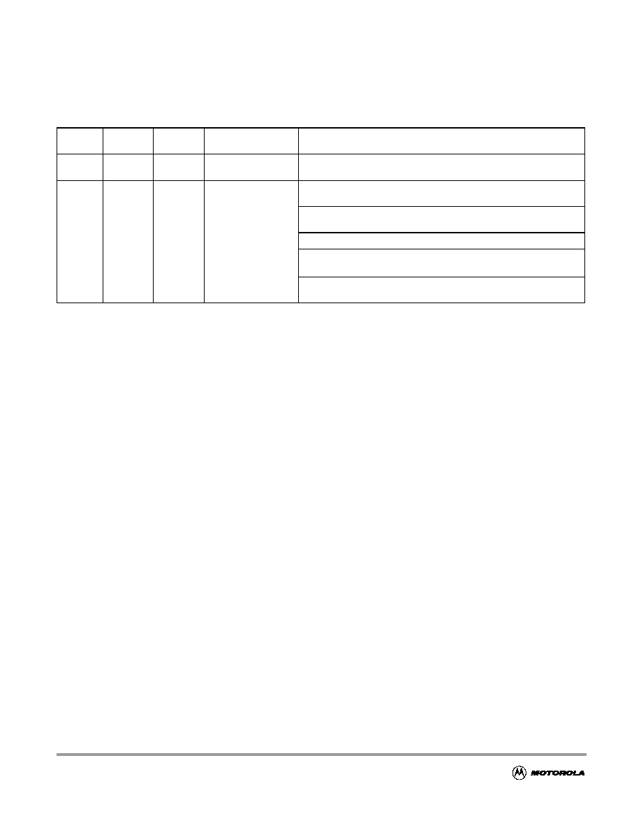
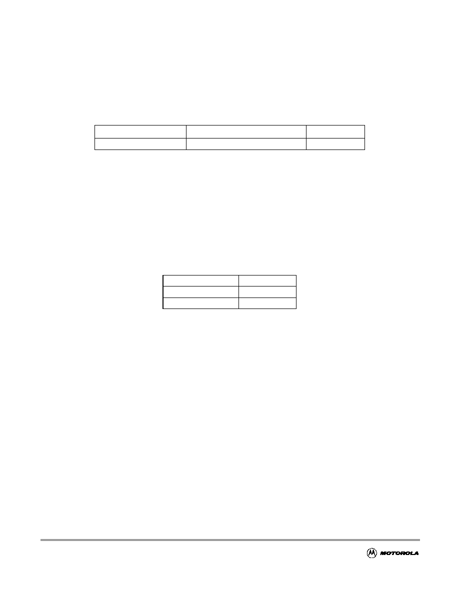
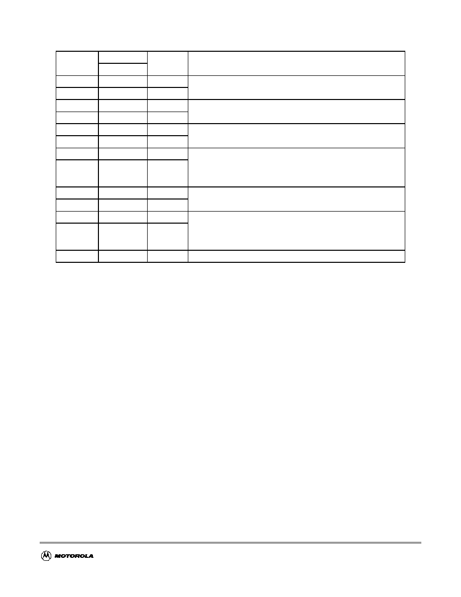
Table 0-1 Document References
User Guide
Version
Document Order Number
HCS12 Core User Guide
V01
HCS12COREUG/D
CRG Block Guide
V03
S12CRGV3/D
ECT_16B8C Block Guide
V01
S12ECT16B8CV1/D
ATD_10B8C Block Guide
V02
S12ATD10B8CV2/D
IIC Block Guide
V02
S12IICV2/D
SCI Block Guide
V02
S12SCIV2/D
SPI Block Guide
V02
S12SPIV2/D
PWM_8B8C Block Guide
V01
S12PWM8B8CV1/D
FTS128K Block Guide
V02
S12FTS128KV1/D
EETS2K Block Guide
V02
S12EETS2KV1/D
VREG Block Guide
V01
S12VREGV1/D
PIM_9A128 Block Guide
V01
S12A128PIMV1/D

MC9S12A128 Device Guide -- V01.01
14

MC9S12A128 Device Guide -- V01.01
15
Section 1 Introduction
1.1 Overview
The MC9S12A128 microcontroller unit (MCU) is a 16-bit device composed of standard on-chip
peripherals including a 16-bit central processing unit (HCS12 CPU), 128K bytes of Flash EEPROM, 8K
bytes of RAM, 2K bytes of EEPROM, two asynchronous serial communications interfaces (SCI), two
serial peripheral interfaces (SPI), an 8-channel IC/OC enhanced capture timer, two 8-channel, 10-bit
analog-to-digital converters (ADC), an 8-channel pulse-width modulator (PWM), 29 discrete digital I/O
channels (Port A, Port B, Port K and Port E), 20 discrete digital I/O lines with interrupt and wakeup
capability and an Inter-IC Bus. System resource mapping, clock generation, interrupt control and bus
interfacing are managed by the System Integration Module (SIM). The MC9S12A128 has full 16-bit data
paths throughout. However, the external bus can operate in an 8-bit narrow mode so single 8-bit wide
memory can be interfaced for lower cost systems. The inclusion of a PLL circuit allows power
consumption and performance to be adjusted to suit operational requirements.
1.2 Features
∑
HCS12 Core
≠
16-bit HCS12 CPU
i. Upward compatible with M68HC11 instruction set
ii. Interrupt stacking and programmer's model identical to M68HC11
iii. Instruction queue
iv. Enhanced indexed addressing
≠
MEBI (Multiplexed External Bus Interface)
≠
MMC (Module Mapping Control)
≠
INT (Interrupt control)
≠
BKP (Breakpoints)
≠
BDM (Background Debug Mode)
∑
CRG (low current oscillator, PLL, reset, clocks, COP watchdog, real time interrupt, clock monitor)
∑
8-bit and 4-bit ports with interrupt functionality
≠
Digital filtering
≠
Programmable rising or falling edge trigger
∑
Memory
≠
128K Flash EEPROM
≠
2K byte EEPROM
≠
8K byte RAM

MC9S12A128 Device Guide -- V01.01
16
∑
Two 8-channel Analog-to-Digital Converters
≠
10-bit resolution
≠
External conversion trigger capability
∑
Enhanced Capture Timer
≠
16-bit main counter with 7-bit prescaler
≠
8 programmable input capture or output compare channels
≠
Two 8-bit or one 16-bit pulse accumulators
∑
8 PWM channels
≠
Programmable period and duty cycle
≠
8-bit 8-channel or 16-bit 4-channel
≠
Separate control for each pulse width and duty cycle
≠
Center-aligned or left-aligned outputs
≠
Programmable clock select logic with a wide range of frequencies
≠
Fast emergency shutdown input
≠
Usable as interrupt inputs
∑
Serial interfaces
≠
Two asynchronous Serial Communications Interfaces (SCI)
≠
Two Synchronous Serial Peripheral Interface (SPI)
∑
Inter-IC Bus (IIC)
≠
Compatible with I2C Bus standard
≠
Multi-master operation
≠
Software programmable for one of 256 different serial clock frequencies
∑
112-Pin LQFP and 80-pin QFP packages
≠
I/O lines with 5V input and drive capability
≠
5V A/D converter inputs
≠
Operation at 50MHz equivalent to 25MHz Bus Speed
≠
Development support
≠
Single-wire background debugTM mode (BDM)
≠
On-chip hardware breakpoints

MC9S12A128 Device Guide -- V01.01
17
1.3 Modes of Operation
User modes
∑
Normal and Emulation Operating Modes
≠
Normal Single-Chip Mode
≠
Normal Expanded Wide Mode
≠
Normal Expanded Narrow Mode
≠
Emulation Expanded Wide Mode
≠
Emulation Expanded Narrow Mode
∑
Special Operating Modes
≠
Special Single-Chip Mode with active Background Debug Mode
≠
Special Test Mode (Motorola use only)
≠
Special Peripheral Mode (Motorola use only)
Low power modes
∑
Stop Mode
∑
Pseudo Stop Mode
∑
Wait Mode

MC9S12A128 Device Guide -- V01.01
18
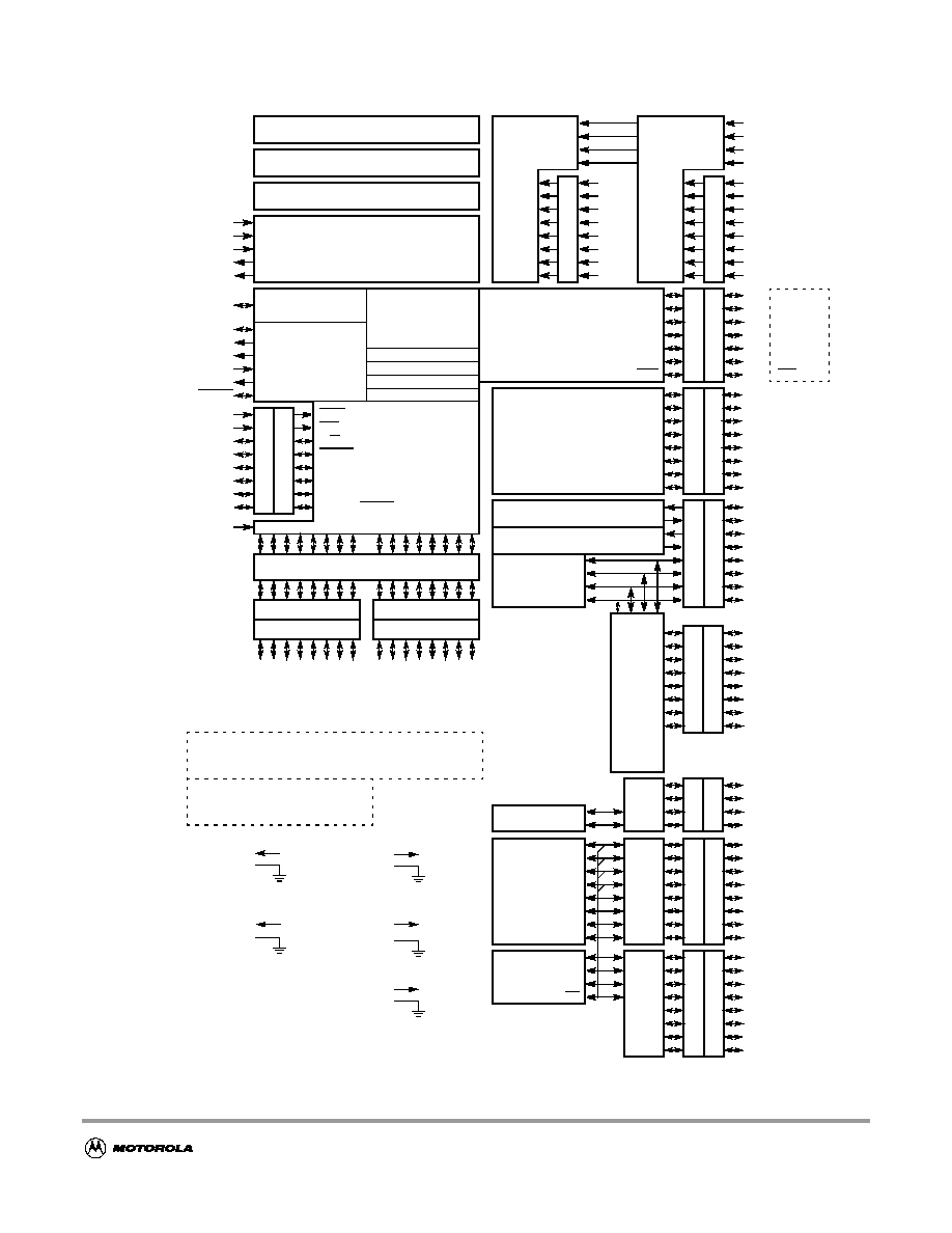
1.4 Block Diagram
Figure 1-1
shows a block diagram of the MC9S12A128 device.
MC9S12A128 Device Guide -- V01.01
19
Figure 1-1 MC9S12A128 Block Diagram
128K Byte Flash EEPROM
8K Byte RAM
Enhanced Capture
RESET
EXTAL
XTAL
VDD1,2
VSS1,2
SCI0
2K Byte EEPROM
BKGD
R/W
MODB
XIRQ
NOACC/XCLKS
System
Integration
Module
(SIM)
VDDR
CPU12
Periodic Interrupt
COP Watchdog
Clock Monitor
Single-wire Background
Breakpoints
PLL
VSSPLL
XFC
VDDPLL
Multiplexed Address/Data Bus
VDDA
VSSA
VRH
VRL
ATD0
Multiplexed
Wide Bus
Multiplexed
VDDX
VSSX
Internal Logic 2.5V
Narrow Bus
PPAGE
VDDPLL
VSSPLL
PLL 2.5V
IRQ
LSTRB
ECLK
MODA
PA
4
PA
3
PA
2
PA
1
PA
0
PA
7
PA
6
PA
5
TEST
A
DDR
1
2
A
DDR
1
1
A
DDR
1
0
A
DDR
9
A
DDR
8
A
DDR
1
5
A
DDR
1
4
A
DDR1
3
DA
T
A
1
2
DA
T
A
1
1
DA
T
A
1
0
DA
T
A
9
DA
T
A
8
DA
T
A
1
5
DA
T
A
1
4
DA
T
A
1
3
PB
4
PB
3
PB
2
PB
1
PB
0
PB
7
PB
6
PB
5
A
DDR
4
A
DDR
3
A
DDR
2
A
DDR
1
A
DDR
0
A
DDR
7
A
DDR
6
A
DDR
5
DA
T
A
4
DA
T
A
3
DA
T
A
2
DA
T
A
1
DA
T
A
0
DA
T
A
7
DA
T
A
6
DA
T
A
5
DA
T
A
4
DA
T
A
3
DA
T
A
2
DA
T
A
1
DA
T
A
0
DA
T
A
7
DA
T
A
6
DA
T
A
5
PE3
PE4
PE5
PE6
PE7
PE0
PE1
PE2
AN2
AN6
AN0
AN7
AN1
AN3
AN4
AN5
PAD03
PAD04
PAD05
PAD06
PAD07
PAD00
PAD01
PAD02
IOC2
IOC6
IOC0
IOC7
IOC1
IOC3
IOC4
IOC5
PT3
PT4
PT5
PT6
PT7
PT0
PT1
PT2
VRH
VRL
VDDA
VSSA
VRH
VRL
ATD1
AN2
AN6
AN0
AN7
AN1
AN3
AN4
AN5
PAD11
PAD12
PAD13
PAD14
PAD15
PAD08
PAD09
PAD10
VDDA
VSSA
RXD
TXD
MISO
MOSI
PS3
PS4
PS5
PS0
PS1
PS2
SCI1
RXD
TXD
PP3
PP4
PP5
PP6
PP7
PP0
PP1
PP2
PIX2
PIX0
PIX1
PIX3
ECS
PK3
PK7
PK0
PK1
XADDR17
ECS
XADDR14
XADDR15
XADDR16
SCK
SS
PS6
PS7
SPI0
IIC
SDA
SCL
PJ6
PJ7
PM1
PM0
PM2
PM3
PM4
PM5
PM6
PM7
KWH2
KWH6
KWH0
KWH7
KWH1
KWH3
KWH4
KWH5
PH3
PH4
PH5
PH6
PH7
PH0
PH1
PH2
KWJ0
KWJ1
PJ0
PJ1
I/O Driver 5V
VDDA
VSSA
A/D Converter 5V &
DDRA
DDRB
PTA
PTB
D
DRE
PT
E
AD
1
AD
0
PT
K
DDR
K
PT
T
D
DRT
PT
P
DD
RP
PT
S
D
DRS
PT
M
DDR
M
PT
H
DD
RH
PT
J
DD
RJ
PK2
Clock and
Reset
Generation
Module
Voltage Regulator
VSSR
Debug Module
VDD1,2
VSS1,2
VREGEN
VDDR
VSSR
Voltage Regulator 5V & I/O
MISO
MOSI
SCK
SS
SPI1
PIX4
PIX5
PK4
PK5
XADDR18
XADDR19
Voltage Regulator Reference
KWP2
KWP6
KWP0
KWP7
KWP1
KWP3
KWP4
KWP5
KWJ6
KWJ7
Timer
S
i
gna
l
s
s
how
n
i
n
Bo
l
d
a
r
e not
av
ai
l
abl
e
on the 80 P
i
n
P
a
c
k
a
g
e
M
o
d
u
l
e
to
Po
r
t
R
o
u
t
i
n
g
PWM2
PWM6
PWM0
PWM7
PWM1
PWM3
PWM4
PWM5
PWM
MC9S12A128 Device Guide -- V01.01
20
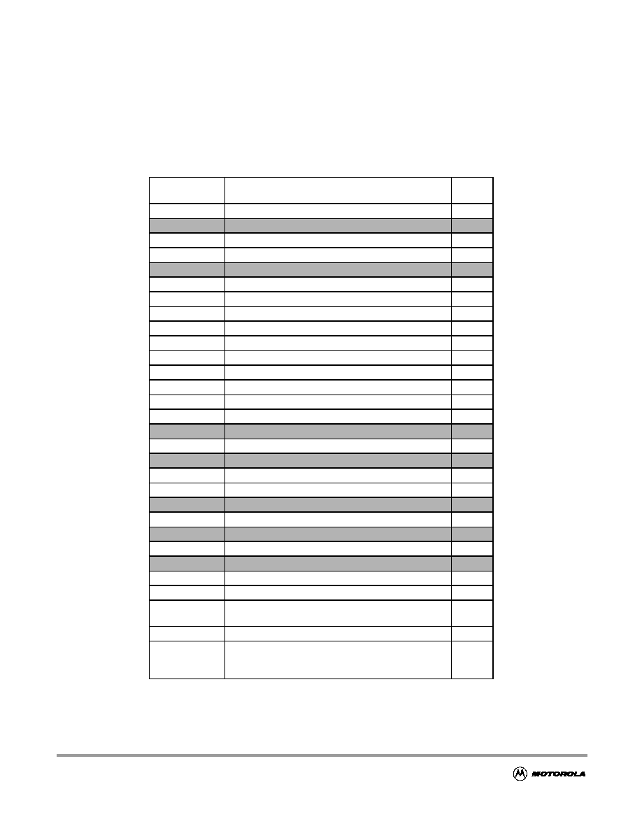
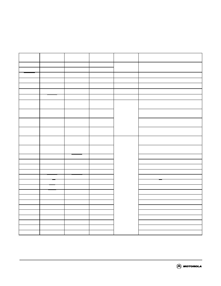
1.5 Device Memory Map
Table 1-1
and
Figure 1-2
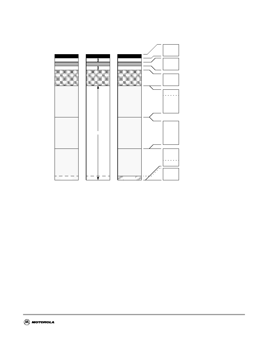
show the device memory map of the MC9S12A128 after reset. Note that after
reset the bottom 1K of the EEPROM ($0000 - $03FF) are hidden by the register space.
Table 1-1 Device Memory Map
Address
Module
Size
(Bytes)
$0000 ≠ $0017
CORE (Ports A, B, E, Modes, Inits, Test)
24
$0018 ≠ $0019
Reserved
2
$001A ≠ $001B Device ID register (PARTID)
2
$001C ≠ $001F CORE (MEMSIZ, IRQ, HPRIO)
4
$0020 ≠ $0027
Reserved
8
$0028 ≠ $002F
CORE (Background Debug Mode)
8
$0030 ≠ $0033
CORE (PPAGE, Port K)
4
$0034 ≠ $003F
Clock and Reset Generator (PLL, RTI, COP)
12
$0040 ≠ $007F
Enhanced Capture Timer 16-bit 8 channels
64
$0080 ≠ $009F
Analog to Digital Converter 10-bit 8 channels (ATD0)
32
$00A0 ≠ $00C7 Pulse Width Modulator 8-bit 8 channels (PWM)
40
$00C8 ≠ $00CF Serial Communications Interface 0 (SCI0)
8
$00D0 ≠ $00D7 Serial Communications Interface 0 (SCI1)
8
$00D8 ≠ $00DF Serial Peripheral Interface (SPI0)
8
$00E0 ≠ $00E7 Inter IC Bus
8
$00E8 ≠ $00EF Reserved
8
$00F0 ≠ $00F7
Serial Peripheral Interface (SPI1)
8
$00F8 ≠ $00FF Reserved
8
$0100- $010F
Flash Control Register
16
$0110 ≠ $011B
EEPROM Control Register
12
$011C ≠ $011F
Reserved
4
$0120 ≠ $013F
Analog to Digital Converter 10-bit 8 channels (ATD1)
32
$0140 ≠ $023F
Reserved
256
$0240 ≠ $027F
Port Integration Module (PIM)
64
$0280 ≠ $03FF
Reserved
384
$0000 ≠ $07FF
EEPROM array
2048
$0000 ≠ $1FFF RAM array
8192
$4000 ≠ $7FFF
Fixed Flash EEPROM array
incl. 0.5K, 1K, 2K or 4K Protected Sector at start
16384
$8000 ≠ $BFFF Flash EEPROM Page Window
16384
$C000 ≠ $FFFF
Fixed Flash EEPROM array
incl. 0.5K, 1K, 2K or 4K Protected Sector at end
and 256 bytes of Vector Space at $FF80 ≠ $FFFF
16384
MC9S12A128 Device Guide -- V01.01
21
Figure 1-2 MC9S12A128 Memory Map
$0000
$FFFF
$C000
$8000
$4000
$0400
$0800
$1000
$2000
$FF00
EXT
NORMAL
SINGLE CHIP
EXPANDED
SPECIAL
SINGLE CHIP
VECTORS
VECTORS
VECTORS
$FF00
$FFFF
BDM
(If Active)
$C000
$FFFF
16K Fixed Flash EEPROM
2K, 4K, 8K or 16K Protected Boot Sector
$8000
$BFFF
16K Page Window
eight * 16K Flash EEPROM Pages
$4000
$7FFF
16K Fixed Flash EEPROM
0.5K, 1K, 2K or 4K Protected Sector
$2000
$3FFF
8K Bytes RAM
Mappable to any 8K Boundary
$0800
$0FFF
2K Bytes EEPROM
Mappable to any 2K Boundary
$0000
$03FF
1K Register Space
Mappable to any 2K Boundary
The address does not show the map after reset, but a useful map. After reset the map is:
$0000 ≠ $03FF: Register Space
$0000 ≠ $1FFF: 8K RAM
$0000 ≠ $07FF: 2K EEPROM (not visible)
$2000 ≠ $3FFF: 8K Flash
MC9S12A128 Device Guide -- V01.01
22
1.6 Part ID Assignments
The part ID is located in two 8-bit registers PARTIDH and PARTIDL (addresses $001A and $001B after
reset). The read-only value is a unique part ID for each revision of the chip.
Table 1-2
shows the assigned
part ID number.
The device memory sizes are located in two 8-bit registers MEMSIZ0 and MEMSIZ1 (addresses $001C
and $001D after reset).
Table 1-3
shows the read-only values of these registers. Refer to the HCS12 Core
User Guide (Motorola document order number HCS12COREUG/D) for further details.
Table 1-2 Assigned Part ID Numbers
Device
Mask Set Number
Part ID
1
NOTES
:
1. The coding is as follows:
Bit 15-12: Major family identifier
Bit 11-8: Minor family identifier
Bit 7-4: Major mask set revision number including FAB transfers
Bit 3-0: Minor - non full - mask set revision
MC9S12A128
0L85D
$0100
Table 1-3 Memory Size Registers
Register name
Value
MEMSIZ0
$13
MEMSIZ1
$80

MC9S12A128 Device Guide -- V01.01
23
Section 2 Signal Description
This section describes signals that connect off-chip. It includes a pinout diagram, a table of signal
properties, and detailed discussion of signals. It is built from the signal description sections of the Block
Guides of the individual IP blocks on the device.
2.1 Device Pinout
The MC9S12A128 is available in a 112-pin low profile quad flat pack (LQFP) and is also available in a
80-pin quad flat pack (QFP). Most pins perform two or more functions, as described in the
2.3 Detailed
Signal Descriptions
.
Figure 2-1
and
Figure 2-2
show the pin assignments.

MC9S12A128 Device Guide -- V01.01
24
Figure 2-1 Pin Assignments in 112-Pin LQFP
VRH
VDDA
PAD15/AN15/ETRIG1
PAD07/AN07/ETRIG0
PAD14/AN14
PAD06/AN06
PAD13/AN13
PAD05/AN05
PAD12/AN12
PAD04/AN04
PAD11/AN11
PAD03/AN03
PAD10/AN10
PAD02/AN02
PAD09/AN09
PAD01/AN01
PAD08/AN08
PAD00/AN00
VSS2
VDD2
PA7/ADDR15/DATA15
PA6/ADDR14/DATA14
PA5/ADDR13/DATA13
PA4/ADDR12/DATA12
PA3/ADDR11/DATA11
PA2/ADDR10/DATA10
PA1/ADDR9/DATA9
PA0/ADDR8/DATA8
PP4/
K
W
P
4/
PW
M
4
PP5/
KPW
5/
PW
M
5
PP6/
K
W
P
6/
P
W
M
6
PP7/
K
W
P
7/
PW
M
7
PK
7/
E
C
S
VD
D
X
VSSX
PM
0
PM
1
PM
2/
M
I
SO0
PM
3/
S
S
0
PM
4/
M
O
S
I
P
M
5
/
SC
K0
PJ
6/
K
W
J
6
/
S
D
A
PJ
7/
K
W
J
7
/
S
C
L
VR
EGEN
PS7/
SS0
PS6/
S
C
K
0
P
S
5
/MO
S
I0
PS4/
M
I
S
O0
PS3/
T
XD
1
PS2/
R
XD
1
PS1/
T
XD
0
PS0/
R
XD
0
PM
6
PM
7
VSSA
VR
L
SS1/PWM3/KWP3/PP3
SCK1/PWM2/KWP2/PP2
MOSI1/PWM1/KWP1/PP1
MISO1/PWM0/KWP0/PP0
XADDR17/PK3
XADDR16/PK2
XADDR15/PK1
XADDR14/PK0
IOC0/PT0
IOC1/PT1
IOC2/PT2
IOC3/PT3
VDD1
VSS1
IOC4/PT4
IOC5/PT5
IOC6/PT6
IOC7/PT7
XADDR19/PK5
XADDR18/PK4
KWJ1/PJ1
KWJ0/PJ0
MODC/TAGHI/BKGD
ADDR0/DATA0/PB0
ADDR1/DATA1/PB1
ADDR2/DATA2/PB2
ADDR3/DATA3/PB3
ADDR4/DATA4/PB4
AD
D
R
5
/
D
A
T
A
5
/
P
B5
AD
D
R
6
/
D
A
T
A
6
/
P
B6
AD
D
R
7
/
D
A
T
A
7
/
P
B7
K
W
H7
/P
H7
K
W
H6
/P
H6
K
W
H5
/P
H5
K
W
H4
/P
H4
XC
LKS
/NO
A
CC/
P
E
7
M
O
D
B
/
I
PI
PE1
/
P
E
6
M
O
D
A
/
I
PI
PE0
/
P
E
5
EC
L
K
/
P
E4
V
SSR
VD
D
R
R
ESET
VD
D
P
LL
XF
C
VSSP
LL
EX
T
A
L
XT
A
L
T
EST
SS
1
/K
WH3
/
P
H
3
S
CK1
/K
WH2
/
P
H
2
MO
S
I
1
/
K
W
H1
/P
H1
MI
S
O
1
/
K
W
H0
/P
H0
LS
T
R
B
/T
A
G
L
O
/P
E
3
R/
W
/P
E
2
IR
Q
/P
E
1
XI
R
Q
/P
E
0
Signals shown in Bold are not available on the 80 Pin Package
MC9S12A128
11
2
111
11
0
109
108
107
106
105
104
103
102
101
100
99
98
97
96
95
94
93
92
91
90
89
88
87
86
85
1
2
3
4
5
6
7
8
9
10
11
12
13
14
15
16
17
18
19
20
21
22
23
24
25
26
27
28
29
30
31
32
33
34
35
36
37
38
39
40
41
42
43
44
45
46
47
48
49
50
51
52
53
54
55
56
84
83
82
81
80
79
78
77
76
75
74
73
72
71
70
69
68
67
66
65
64
63
62
61
60
59
58
57

MC9S12A128 Device Guide -- V01.01
25
Figure 2-2 Pin Assignments in 80-Pin QFP for MC9S12A128
1
2
3
4
5
6
7
8
9
10
11
12
13
14
15
16
17
18
19
20
80
79
78
77
76
75
74
73
72
71
70
69
68
67
66
65
64
63
62
61
21
22
23
24
25
26
27
28
29
30
31
32
33
34
35
36
37
38
39
40
MC9S12A128
VRH
VDDA
PAD07/AN07/ETRIG0
PAD06/AN06
PAD05/AN05
PAD04/AN04
PAD03/AN03
PAD02/AN02
PAD01/AN01
PAD00/AN00
VSS2
VDD2
PA7/ADDR15/DATA15
PA6/ADDR14/DATA14
PA5/ADDR13/DATA13
PA4/ADDR12/DATA12
PA3/ADDR11/DATA11
PA2/ADDR10/DATA10
PA1/ADDR9/DATA9
PA0/ADDR8/DATA8
P
P
4/
KW
P4/
P
W
M
4
P
P
5/
KW
P5/
P
W
M
5
P
P
7/
KW
P7/
P
W
M
7
VD
D
X
V
SSX
PM
0
PM
1
PM
2
/
M
I
SO
0
PM
3
/
S
S
0
PM
4
/
M
O
S
I
0
P
M
5/
SC
K0
PJ
6
/
K
W
J
6
/
S
D
A
PJ
7
/
K
W
J
7
/
S
C
L
V
R
EG
EN
PS
3
/
T
X
D
1
PS
2
/
R
X
D
1
PS
1
/
T
X
D
0
PS
0
/
R
X
D
0
V
SSA
VR
L
SS1/PWM3/KWP3/PP3
SCK1/PWM2/KWP2/PP2
MOSI1/PWM1/KWP1/PP1
MISO1/PWM0/KWP0/PP0
IOC0/PT0
IOC1/PT1
IOC2/PT2
IOC3/PT3
VDD1
VSS1
IOC4/PT4
IOC5/PT5
IOC6/PT6
IOC7/PT7
MODC/TAGHI/BKGD
ADDR0/DATA0/PB0
ADDR1/DATA1/PB1
ADDR2/DATA2/PB2
ADDR3/DATA3/PB3
ADDR4/DATA4/PB4
A
DDR5
/
D
A
T
A
5
/P
B
5
A
DDR6
/
D
A
T
A
6
/P
B
6
A
DDR7
/
D
A
T
A
7
/P
B
7
XC
L
K
S
/N
O
A
CC
/P
E
7
M
O
D
B
/
I
PI
PE1/
PE6
M
O
D
A
/
I
PI
PE0/
PE5
EC
LK/
PE4
VS
SR
V
DDR
RE
S
E
T
VD
D
P
L
L
XF
C
V
SSPLL
EXT
AL
XT
AL
TE
S
T
LS
T
R
B
/T
A
G
L
O
/
PE3
R/W
/
PE2
IR
Q
/
PE1
XI
R
Q
/
PE0
60
59
58
57
56
55
54
53
52
51
50
49
48
47
46
45
44
43
42
41
MC9S12A128 Device Guide -- V01.01
26
2.2 Signal Properties Summary
Table 2-1
summarizes the pin functionality. Signals shown in bold are not available in the 80 pin
package.
Table 2-1 Signal Properties
Pin Name
Function 1
Pin Name
Function 2
Pin Name
Function 3
Pin Name
Function 4
Powered by
Description
EXTAL
--
--
--
V
DDPLL
Oscillator Pins
XTAL
--
--
--
RESET
--
--
--
V
DDR
External Reset
TEST
--
--
--
N.A.
Test Input
VREGEN
--
--
--
V
DDX
Voltage Regulator Enable Input
XFC
--
--
--
V
DDPLL
PLL Loop Filter
BKGD
TAGHI
MODC
--
V
DDR
Background Debug, Tag High, Mode Input
PAD15
AN15
ETRIG1
--
V
DDA
Port AD Input, Analog Input AN7 of
ATD1, External Trigger Input of ATD1
PAD[14:8]
AN[14:08]
--
--
Port AD Inputs, Analog Inputs AN[6:0]
of ATD1
PAD07
AN07
ETRIG0
--
Port AD Input, Analog Input AN7 of ATD0,
External Trigger Input of ATD0
PAD[06:00]
AN[06:00]
--
--
Port AD Inputs, Analog Inputs AN[6:0] of
ATD0
PA[7:0]
ADDR[15:8]/
DATA[15:8]
--
--
V
DDR
Port A I/O, Multiplexed Address/Data
PB[7:0]
ADDR[7:0]/
DATA[7:0]
--
--
Port B I/O, Multiplexed Address/Data
PE7
NOACC
XCLKS
--
Port E I/O, Access, Clock Select
PE6
IPIPE1
MODB
--
Port E I/O, Pipe Status, Mode Input
PE5
IPIPE0
MODA
--
Port E I/O, Pipe Status, Mode Input
PE4
ECLK
--
--
Port E I/O, Bus Clock Output
PE3
LSTRB
TAGLO
--
Port E I/O, Byte Strobe, Tag Low
PE2
R/W
--
--
Port E I/O, R/W in expanded modes
PE1
IRQ
--
--
Port E Input, Maskable Interrupt
PE0
XIRQ
--
--
Port E Input, Non Maskable Interrupt
PH7
KWH7
--
--
Port H I/O, Interrupt
PH6
KWH6
--
--
Port H I/O, Interrupt
PH5
KWH5
--
--
Port H I/O, Interrupt
PH4
KWH4
--
--
Port H I/O, Interrupt
PH3
KWH3
SS1
--
Port H I/O, Interrupt, SS of SPI1
PH2
KWH2
SCK1
--
Port H I/O, Interrupt, SCK of SPI1
PH1
KWH1
MOSI1
--
Port H I/O, Interrupt, MOSI of SPI1
PH0
KWH0
MISO1
--
Port H I/O, Interrupt, MISO of SPI1
MC9S12A128 Device Guide -- V01.01
27
PJ7
KWJ7
SCL
V
DDX
Port J I/O, Interrupt, SCL of IIC
PJ6
KWJ6
SDA
Port J I/O, Interrupt, SDA of IIC
PJ[1:0]
KWJ[1:0]
--
--
Port J I/O, Interrupts
PK7
ECS
ROMON
--
Port K I/O, Emulation Chip Select, ROM
On Enable
PK[5:0]
XADDR[19:14]
--
Port K I/O, Extended Addresses
PM7
--
--
--
Port M I/O
PM6
--
--
--
Port M I/O
PM5
SCK0
--
--
Port M I/O, SCK of SPI0
PM4
MOSI0
--
--
Port M I/O, MOSI of SPI0
PM3
SS0
--
--
Port M I/O, SS of SPI0
PM2
MISO0
--
--
Port M I/O, MISO of SPI0
PM1
--
--
--
Port M I/O
PM0
--
--
--
Port M I/O
PP7
KWP7 PWM7
--
Port P I/O, Interrupt, Channel 7 of PWM
PP6
KWP6
PWM6
--
Port P I/O, Interrupt, Channel 6 of PWM
PP5
KWP5 PWM5
--
Port P I/O, Interrupt, Channel 5 of PWM
PP4
KWP4
PWM4
--
Port P I/O, Interrupt, Channel 4 of PWM
PP3
KWP3 PWM3
SS1
Port P I/O, Interrupt, Channel 3 of PWM,
SS of SPI1
PP2
KWP2
PWM2
SCK1
Port P I/O, Interrupt, Channel 2 of PWM,
SCK of SPI1
PP1
KWP1 PWM1
MOSI1
Port P I/O, Interrupt, Channel 1 of PWM,
MOSI of SPI1
PP0
KWP0
PWM0
MISO1
Port P I/O, Interrupt, Channel 0 of PWM,
MISO of SPI1
PS7
SS0
--
--
Port S I/O, SS of SPI0
PS6
SCK0
--
--
Port S I/O, SCK of SPI0
PS5
MOSI0
--
--
Port S I/O, MOSI of SPI0
PS4
MISO0
--
--
Port S I/O, MISO of SPI0
PS3
TXD1
--
--
Port S I/O, TXD of SCI1
PS2
RXD1
--
--
Port S I/O, RXD of SCI1
PS1
TXD0
--
--
Port S I/O, TXD of SCI0
PS0
RXD0
--
--
Port S I/O, RXD of SCI0
PT[7:0]
IOC[7:0]
--
--
Port T I/O, Timer channels
Pin Name
Function 1
Pin Name
Function 2
Pin Name
Function 3
Pin Name
Function 4
Powered by
Description
MC9S12A128 Device Guide -- V01.01
28
2.3 Detailed Signal Descriptions
2.3.1 EXTAL, XTAL -- Oscillator Pins
EXTAL and XTAL are the crystal driver and external clock pins. On reset all the device clocks are derived
from the EXTAL input frequency. XTAL is the crystal output.
2.3.2 RESET -- External Reset Pin
An active low bidirectional control signal, it acts as an input to initialize the MCU to a known start-up state,
and an output when an internal MCU function causes a reset.
2.3.3 TEST -- Test Pin
This input only pin is reserved for test.
NOTE:
The TEST pin must be tied to V
SS
in all applications.
2.3.4 V
REGEN
-- Voltage Regulator Enable Pin
This input only pin enables or disables the on-chip voltage regulator.
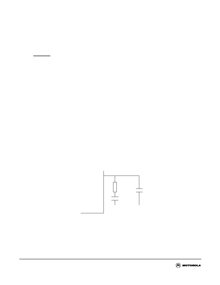
2.3.5 XFC -- PLL Loop Filter Pin
PLL loop filter, see
A.5.3 Phase Locked Loop
. If needed, contact your Motorola representative for the
interactive application note to compute PLL loop filter elements. Any current leakage on this pin must be
avoided.
Figure 2-3 PLL Loop Filter Connections
MCU
XFC
R
0
C
S
C
P
V
DDPLL
V
DDPLL

MC9S12A128 Device Guide -- V01.01
29
2.3.6 BKGD / TAGHI / MODC -- Background Debug, Tag High, and Mode Pin
The BKGD/TAGHI/MODC pin is used as a pseudo-open-drain pin for the background debug
communication. In MCU expanded modes of operation when instruction tagging is on, an input low on
this pin during the falling edge of E-clock tags the high half of the instruction word being read into the
instruction queue. It is used as a MCU operating mode select pin during reset. The state of this pin is
latched to the MODC bit at the rising edge of RESET.
2.3.7 PAD15 / AN15 / ETRIG1 -- Port AD Input Pin of ATD1
PAD15 is a general purpose input pin and analog input AN7 of the analog to digital converter ATD1. It
can act as an external trigger input for the ATD1.
2.3.8 PAD[14:08] / AN[14:08] -- Port AD Input Pins of ATD1
PAD14 - PAD08 are general purpose input pins and analog inputs AN[6:0] of the analog to digital
converter ATD1.
2.3.9 PAD7 / AN07 / ETRIG0 -- Port AD Input Pin of ATD0
PAD7 is a general purpose input pin and analog input AN7 of the analog to digital converter ATD0. It can
act as an external trigger input for the ATD0.
2.3.10 PAD[06:00] / AN[06:00] -- Port AD Input Pins of ATD0
PAD06 - PAD00 are general purpose input pins and analog inputs AN[6:0] of the analog to digital
converter ATD0.
2.3.11 PA[7:0] / ADDR[15:8] / DATA[15:8] -- Port A I/O Pins
PA7-PA0 are general purpose input or output pins. In MCU expanded modes of operation, these pins are
used for the multiplexed external address and data bus.
2.3.12 PB[7:0] / ADDR[7:0] / DATA[7:0] -- Port B I/O Pins
PB7-PB0 are general purpose input or output pins. In MCU expanded modes of operation, these pins are
used for the multiplexed external address and data bus.
2.3.13 PE7 / NOACC / XCLKS -- Port E I/O Pin 7
PE7 is a general purpose input or output pin. During MCU expanded modes of operation, the NOACC
signal, when enabled, is used to indicate that the current bus cycle is an unused or "free" cycle. This signal
will assert when the CPU is not using the bus.

MC9S12A128 Device Guide -- V01.01
30
The XCLKS input selects between an external clock or oscillator configuration. The state of this pin is
latched at the rising edge of RESET. If the input is a logic low the EXTAL pin is configured for an external
clock drive. If input is a logic high an oscillator circuit is configured on EXTAL and XTAL. Since this pin
is an input with a pull-up device, if the pin is left floating, the default configuration is an oscillator circuit
on EXTAL and XTAL.
2.3.14 PE6 / MODB / IPIPE1 -- Port E I/O Pin 6
PE6 is a general purpose input or output pin. It is used as a MCU operating mode select pin during reset.
The state of this pin is latched to the MODB bit at the rising edge of RESET. This pin is shared with the
instruction queue tracking signal IPIPE1. This pin is an input with a pull-down device which is only active
when RESET is low.
2.3.15 PE5 / MODA / IPIPE0 -- Port E I/O Pin 5
PE5 is a general purpose input or output pin. It is used as a MCU operating mode select pin during reset.
The state of this pin is latched to the MODA bit at the rising edge of RESET. This pin is shared with the
instruction queue tracking signal IPIPE0. This pin is an input with a pull-down device which is only active
when RESET is low.
2.3.16 PE4 / ECLK -- Port E I/O Pin 4
PE4 is a general purpose input or output pin. It can be configured to drive the internal bus clock ECLK.
ECLK can be used as a timing reference.
2.3.17 PE3 / LSTRB / TAGLO -- Port E I/O Pin 3
PE3 is a general purpose input or output pin. In MCU expanded modes of operation, LSTRB can be used
for the low-byte strobe function to indicate the type of bus access and when instruction tagging is on,
TAGLO is used to tag the low half of the instruction word being read into the instruction queue.
2.3.18 PE2 / R/W
--
Port E I/O Pin 2
PE2 is a general purpose input or output pin. In MCU expanded modes of operations, this pin drives the
read/write output signal for the external bus. It indicates the direction of data on the external bus.
2.3.19 PE1 / IRQ -- Port E Input Pin 1
PE1 is a general purpose input pin and the maskable interrupt request input that provides a means of
applying asynchronous interrupt requests. This will wake up the MCU from STOP or WAIT mode.
2.3.20 PE0 / XIRQ -- Port E Input Pin 0
PE0 is a general purpose input pin and the non-maskable interrupt request input that provides a means of
applying asynchronous interrupt requests. This will wake up the MCU from STOP or WAIT mode.

MC9S12A128 Device Guide -- V01.01
31
2.3.21 PH7 / KWH7 -- Port H I/O Pin 7
PH7 is a general purpose input or output pin. It can be configured to generate an interrupt causing the MCU
to exit STOP or WAIT mode.
2.3.22 PH6 / KWH6 -- Port H I/O Pin 6
PH6 is a general purpose input or output pin. It can be configured to generate an interrupt causing the MCU
to exit STOP or WAIT mode.
2.3.23 PH5 / KWH5 -- Port H I/O Pin 5
PH5 is a general purpose input or output pin. It can be configured to generate an interrupt causing the MCU
to exit STOP or WAIT mode.
2.3.24 PH4 / KWH4 -- Port H I/O Pin 4
PH4 is a general purpose input or output pin. It can be configured to generate an interrupt causing the MCU
to exit STOP or WAIT mode.
2.3.25 PH3 / KWH3 / SS1 -- Port H I/O Pin 3
PH3 is a general purpose input or output pin. It can be configured to generate an interrupt causing the MCU
to exit STOP or WAIT mode. It can be configured as slave select pin SS
of the Serial Peripheral Interface
1 (SPI1).
2.3.26 PH2 / KWH2 / SCK1 -- Port H I/O Pin 2
PH2 is a general purpose input or output pin. It can be configured to generate an interrupt causing the MCU
to exit STOP or WAIT mode. It can be configured as serial clock pin SCK
of the Serial Peripheral Interface
1 (SPI1).
2.3.27 PH1 / KWH1 / MOSI1 -- Port H I/O Pin 1
PH1 is a general purpose input or output pin. It can be configured to generate an interrupt causing the MCU
to exit STOP or WAIT mode. It can be configured as master output (during master mode) or slave input
pin (during slave mode) MOSI of the Serial Peripheral Interface 1 (SPI1).
2.3.28 PH0 / KWH0 / MISO1 -- Port H I/O Pin 0
PH0 is a general purpose input or output pin. It can be configured to generate an interrupt causing the MCU
to exit STOP or WAIT mode. It can be configured as master input (during master mode) or slave output
(during slave mode) pin MISO
of the Serial Peripheral Interface 1 (SPI1).

MC9S12A128 Device Guide -- V01.01
32
2.3.29 PJ7 / KWJ7 / SCL -- PORT J I/O Pin 7
PJ7 is a general purpose input or output pin. It can be configured to generate an interrupt causing the MCU
to exit STOP or WAIT mode. It can be configured as the serial clock pin SCL of the IIC module.
2.3.30 PJ6 / KWJ6 / SDA -- PORT J I/O Pin 6
PJ6 is a general purpose input or output pin. It can be configured to generate an interrupt causing the MCU
to exit STOP or WAIT mode. It can be configured as the serial data pin SDA of the IIC module.
2.3.31 PJ[1:0] / KWJ[1:0] -- Port J I/O Pins [1:0]
PJ1 and PJ0 are general purpose input or output pins. They can be configured to generate an interrupt
causing the MCU to exit STOP or WAIT mode.
2.3.32 PK7 / ECS / ROMON -- Port K I/O Pin 7
PK7 is a general purpose input or output pin. During MCU expanded modes of operation, this pin is used
as the emulation chip select output (ECS). During MCU normal expanded modes of operation, this pin is
used to enable the Flash EEPROM memory in the memory map (ROMON). At the rising edge of RESET,
the state of this pin is latched to the ROMON bit.
2.3.33 PK[5:0] / XADDR[19:14] -- Port K I/O Pins [5:0]
PK5-PK0 are general purpose input or output pins. In MCU expanded modes of operation, these pins
provide the expanded address XADDR[19:14] for the external bus.
2.3.34 PM7 -- Port M I/O Pin 7
PM7 is a general purpose input or output pin.
2.3.35 PM6 -- Port M I/O Pin 6
PM6 is a general purpose input or output pin.
2.3.36 PM5 / SCK0 -- Port M I/O Pin 5
PM5 is a general purpose input or output pin. It can be configured as the serial clock pin SCK of the Serial
Peripheral Interface 0 (SPI0).
2.3.37 PM4 / MOSI0 -- Port M I/O Pin 4
PM4 is a general purpose input or output pin. It can be configured as the master output (during master
mode) or slave input pin (during slave mode) MOSI
for the Serial Peripheral Interface 0 (SPI0).

MC9S12A128 Device Guide -- V01.01
33
2.3.38 PM3 / SS0 -- Port M I/O Pin 3
PM3 is a general purpose input or output pin. It can be configured as the slave select pin SS of the Serial
Peripheral Interface 0 (SPI0).
2.3.39 PM2 / MISO0 -- Port M I/O Pin 2
PM2 is a general purpose input or output pin. It can be configured as the master input (during master mode)
or slave output pin (during slave mode) MISO
for the Serial Peripheral Interface 0 (SPI0).
2.3.40 PM1 -- Port M I/O Pin 1
PM1 is a general purpose input or output pin.
2.3.41 PM0 -- Port M I/O Pin 0
PM0 is a general purpose input or output pin.
2.3.42 PP7 / KWP7 / PWM7 -- Port P I/O Pin 7
PP7 is a general purpose input or output pin. It can be configured to generate an interrupt causing the MCU
to exit STOP or WAIT mode. It can be configured as Pulse Width Modulator (PWM) channel 7 output.
2.3.43 PP6 / KWP6 / PWM6 -- Port P I/O Pin 6
PP6 is a general purpose input or output pin. It can be configured to generate an interrupt causing the MCU
to exit STOP or WAIT mode. It can be configured as Pulse Width Modulator (PWM) channel 6 output.
2.3.44 PP5 / KWP5 / PWM5 -- Port P I/O Pin 5
PP5 is a general purpose input or output pin. It can be configured to generate an interrupt causing the MCU
to exit STOP or WAIT mode. It can be configured as Pulse Width Modulator (PWM) channel 5 output.
2.3.45 PP4 / KWP4 / PWM4 -- Port P I/O Pin 4
PP4 is a general purpose input or output pin. It can be configured to generate an interrupt causing the MCU
to exit STOP or WAIT mode. It can be configured as Pulse Width Modulator (PWM) channel 4 output
2.3.46 PP3 / KWP3 / PWM3 / SS1 -- Port P I/O Pin 3
PP3 is a general purpose input or output pin. It can be configured to generate an interrupt causing the MCU
to exit STOP or WAIT mode. It can be configured as Pulse Width Modulator (PWM) channel 3 output. It
can be configured as slave select pin SS
of the Serial Peripheral Interface 1 (SPI1).

MC9S12A128 Device Guide -- V01.01
34
2.3.47 PP2 / KWP2 / PWM2 / SCK1 -- Port P I/O Pin 2
PP2 is a general purpose input or output pin. It can be configured to generate an interrupt causing the MCU
to exit STOP or WAIT mode. It can be configured as Pulse Width Modulator (PWM) channel 2 output. It
can be configured as serial clock pin SCK
of the Serial Peripheral Interface 1 (SPI1).
2.3.48 PP1 / KWP1 / PWM1 / MOSI1 -- Port P I/O Pin 1
PP1 is a general purpose input or output pin. It can be configured to generate an interrupt causing the MCU
to exit STOP or WAIT mode. It can be configured as Pulse Width Modulator (PWM) channel 1 output. It
can be configured as master output (during master mode) or slave input pin (during slave mode) MOSI
of
the Serial Peripheral Interface 1 (SPI1).
2.3.49 PP0 / KWP0 / PWM0 / MISO1 -- Port P I/O Pin 0
PP0 is a general purpose input or output pin. It can be configured to generate an interrupt causing the MCU
to exit STOP or WAIT mode. It can be configured as Pulse Width Modulator (PWM) channel 0 output. It
can be configured as master input (during master mode) or slave output (during slave mode) pin MISO
of
the Serial Peripheral Interface 1 (SPI1).
2.3.50 PS7 / SS0 -- Port S I/O Pin 7
PS7 is a general purpose input or output pin. It can be configured as the slave select pin SS of the Serial
Peripheral Interface 0 (SPI0).
2.3.51 PS6 / SCK0 -- Port S I/O Pin 6
PS6 is a general purpose input or output pin. It can be configured as the serial clock pin SCK of the Serial
Peripheral Interface 0 (SPI0).
2.3.52 PS5 / MOSI0 -- Port S I/O Pin 5
PS5 is a general purpose input or output pin. It can be configured as master output (during master mode)
or slave input pin (during slave mode) MOSI
of the Serial Peripheral Interface 0 (SPI0).
2.3.53 PS4 / MISO0 -- Port S I/O Pin 4
PS4 is a general purpose input or output pin. It can be configured as master input (during master mode) or
slave output pin (during slave mode) MOSI
of the Serial Peripheral Interface 0 (SPI0).
2.3.54 PS3 / TXD1 -- Port S I/O Pin 3
PS3 is a general purpose input or output pin. It can be configured as the transmit pin TXD of Serial
Communication Interface 1 (SCI1).

MC9S12A128 Device Guide -- V01.01
35
2.3.55 PS2 / RXD1 -- Port S I/O Pin 2
PS2 is a general purpose input or output pin. It can be configured as the receive pin RXD of Serial
Communication Interface 1 (SCI1).
2.3.56 PS1 / TXD0 -- Port S I/O Pin 1
PS1 is a general purpose input or output pin. It can be configured as the transmit pin TXD of Serial
Communication Interface 0 (SCI0).
2.3.57 PS0 / RXD0 -- Port S I/O Pin 0
PS0 is a general purpose input or output pin. It can be configured as the receive pin RXD of Serial
Communication Interface 0 (SCI0).
2.3.58 PT[7:0] / IOC[7:0] -- Port T I/O Pins [7:0]
PT7-PT0 are general purpose input or output pins. They can be configured as input capture or output
compare pins IOC7-IOC0 of the Enhanced Capture Timer (ECT).
2.4 Power Supply Pins
MC9S12A128 power and ground pins are described below.
NOTE:
All V
SS
pins must be connected together in the application.
2.4.1 V
DDX
, V
SSX
-- Power & Ground Pins for I/O Drivers
External power and ground for I/O drivers. Because fast signal transitions place high, short-duration
current demands on the power supply, use bypass capacitors with high-frequency characteristics and place
them as close to the MCU as possible. Bypass requirements depend on how heavily the MCU pins are
loaded.
2.4.2 V
DDR
, V
SSR
-- Power & Ground Pins for I/O Drivers & for Internal
Voltage Regulator
External power and ground for I/O drivers and input to the internal voltage regulator. Because fast signal
transitions place high, short-duration current demands on the power supply, use bypass capacitors with
high-frequency characteristics and place them as close to the MCU as possible. Bypass requirements
depend on how heavily the MCU pins are loaded.

MC9S12A128 Device Guide -- V01.01
36
2.4.3 V
DD1
, V
DD2
, V
SS1
, V
SS2
-- Core Power Pins
Power is supplied to the MCU through V
DD
and V
SS
. Because fast signal transitions place high,
short-duration current demands on the power supply, use bypass capacitors with high-frequency
characteristics and place them as close to the MCU as possible. This 2.5V supply is derived from the
internal voltage regulator. There is no static load on those pins allowed. The internal voltage regulator is
turned off, if V
REGEN
is tied to ground.
NOTE:
No load allowed except for bypass capacitors.
2.4.4 V
DDA
, V
SSA
-- Power Supply Pins for ATD and VREG
V
DDA
, V
SSA
are the power supply and ground input pins for the voltage regulator and the analog to digital
converter. It also provides the reference for the internal voltage regulator. This allows the supply voltage
to the ATD and the reference voltage to be bypassed independently.
2.4.5 V
RH
, V
RL
-- ATD Reference Voltage Input Pins
V
RH
and V
RL
are the reference voltage input pins for the analog to digital converter.
2.4.6 V
DDPLL
, V
SSPLL
-- Power Supply Pins for PLL
Provides operating voltage and ground for the Oscillator and the Phased-Locked Loop. This allows the
supply voltage to the Oscillator and PLL to be bypassed independently. This 2.5V voltage is generated by
the internal voltage regulator.
NOTE:
No load allowed except for bypass capacitors.
2.4.7 V
REGEN
-- On Chip Voltage Regulator Enable
Enables the internal 5V to 2.5V voltage regulator. If this pin is tied low, V
DD1,2
and V
DDPLL
must be
supplied externally.
MC9S12A128 Device Guide -- V01.01
37
Table 2-2 MC9S12A128 Power and Ground Connection Summary
Mnemonic
Pin Number
Nominal
Voltage
Description
112-pin QFP
V
DD1, 2
13, 65
2.5 V
Internal power and ground generated by internal regulator
V
SS1, 2
14, 66
0V
V
DDR
41
5.0 V
External power and ground, supply to pin drivers and internal
voltage regulator.
V
SSR
40
0 V
V
DDX
107
5.0 V
External power and ground, supply to pin drivers.
V
SSX
106
0 V
V
DDA
83
5.0 V
Operating voltage and ground for the analog-to-digital
converters and the reference for the internal voltage regulator,
allows the supply voltage to the A/D to be bypassed
independently.
V
SSA
86
0 V
V
RL
85
0 V
Reference voltages for the analog-to-digital converter.
V
RH
84
5.0 V
V
DDPLL
43
2.5 V
Provides operating voltage and ground for the Phased-Locked
Loop. This allows the supply voltage to the PLL to be
bypassed independently. Internal power and ground
generated by internal regulator.
V
SSPLL
45
0 V
V
REGEN
97
5V
Internal Voltage Regulator enable/disable

MC9S12A128 Device Guide -- V01.01
38
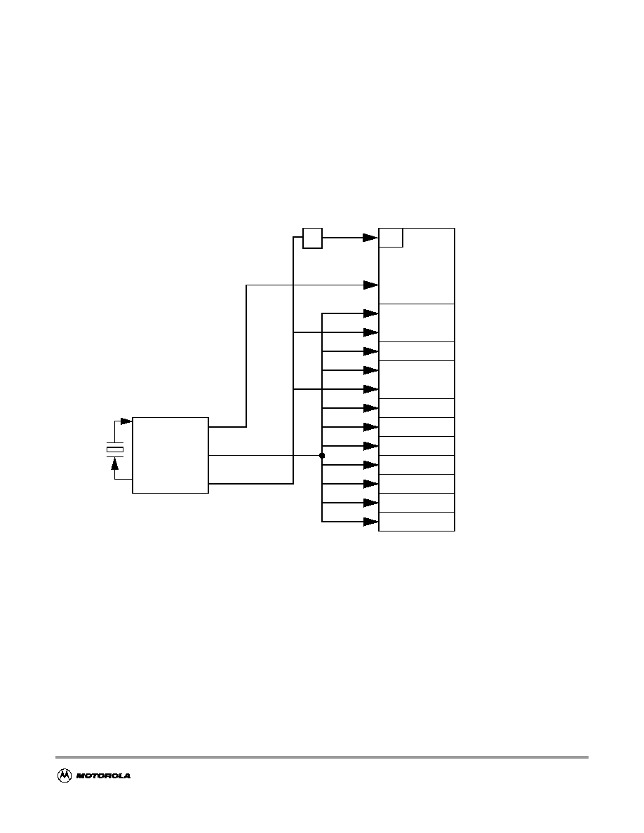
MC9S12A128 Device Guide -- V01.01
39
Section 3 System Clock Description
3.1 Overview
The Clock and Reset Generator provides the internal clock signals for the core and all peripheral modules.
Figure 3-1
shows the clock connections from the CRG to all modules.
Consult the HCS12 Clock and Reset Generator (CRG) Block Guide (Motorola document order number,
S12CRGV3/D) for details on clock generation.
Figure 3-1 Clock Connections
CRG
bus clock
core clock
EXTAL
XTAL
oscillator clock
S12_CORE
IIC
RAM
SCI0, SCI1
PWM
ATD0, 1
EEPROM
Flash
ECT
SPI0, 1
PIM
BDM
1/2

MC9S12A128 Device Guide -- V01.01
40
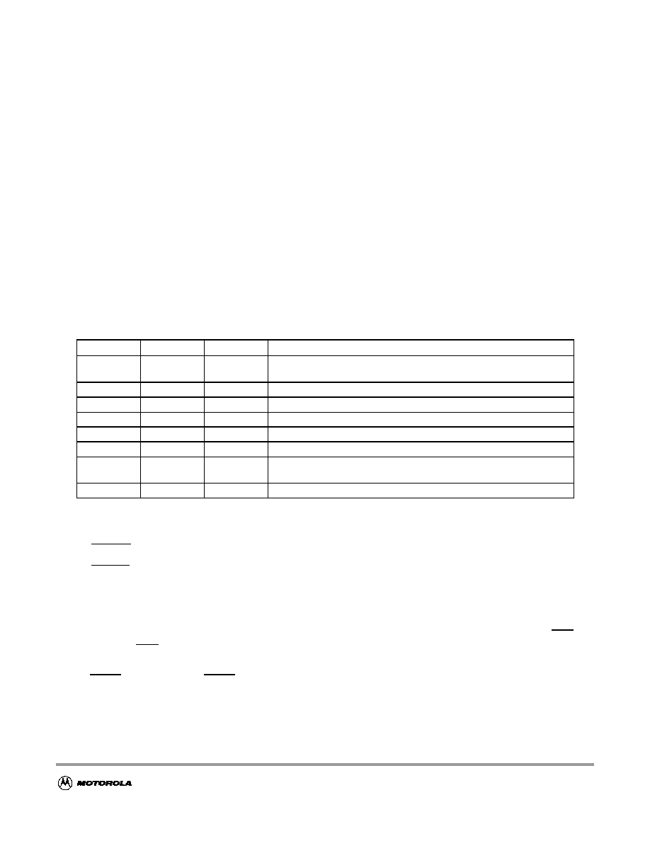
MC9S12A128 Device Guide -- V01.01
41
Section 4 Modes of Operation
4.1 Overview
Eight possible modes determine the operating configuration of the MC9S12A128. Each mode has an
associated default memory map and external bus configuration.
Three low power modes exist for the device.
4.2 Modes of Operation
The operating mode out of reset is determined by the states of the MODC, MODB, and MODA pins during
reset (
Table 4-1
). The MODC, MODB, and MODA bits in the MODE register show the current operating
mode and provide limited mode switching during operation. The states of the MODC, MODB, and MODA
pins are latched into these bits on the rising edge of the reset signal.
There are two basic types of operating modes:
1.
Normal modes: Some registers and bits are protected against accidental changes.
2.
Special modes: Allow greater access to protected control registers and bits for special purposes such
as testing.
A system development and debug feature, background debug mode (BDM), is available in all modes. In
special single-chip mode, BDM is active immediately after reset.
Some aspects of Port E are not mode dependent. Bit 1 of Port E is a general purpose input or the IRQ
interrupt input. IRQ can be enabled by bits in the CPU's condition codes register but it is inhibited at reset
so this pin is initially configured as a simple input with a pull-up. Bit 0 of Port E is a general purpose input
or the XIRQ interrupt input. XIRQ can be enabled by bits in the CPU's condition codes register but it is
inhibited at reset so this pin is initially configured as a simple input with a pull-up. The ESTR bit in the
EBICTL register is set to one by reset in any user mode. This assures that the reset vector can be fetched
Table 4-1 Mode Selection
MODC
MODB
MODA Mode
Description
0
0
0
Special Single Chip, BDM allowed and ACTIVE. BDM is allowed in all
other modes but a serial command is required to make BDM active.
0
0
1
Emulation Expanded Narrow, BDM allowed
0
1
0
Special Test (Expanded Wide), BDM allowed
0
1
1
Emulation Expanded Wide, BDM allowed
1
0
0
Normal Single Chip, BDM allowed
1
0
1
Normal Expanded Narrow, BDM allowed
1
1
0
Peripheral; BDM allowed but bus operations would cause bus conflicts
(must not be used)
1
1
1
Normal Expanded Wide, BDM allowed

MC9S12A128 Device Guide -- V01.01
42
even if it is located in an external slow memory device. The PE6/MODB/IPIPE1 and PE5/MODA/IPIPE0
pins act as high-impedance mode select inputs during reset.
The following paragraphs discuss the default bus setup and describe which aspects of the bus can be
changed after reset on a per mode basis.
4.2.1 Normal Operating Modes
These modes provide three operating configurations. Background debug is available in all three modes,
but must first be enabled for some operations by means of a BDM background command, then activated.
4.2.1.1 Normal Single-Chip Mode
There is no external expansion bus in this mode. All pins of Ports A, B and E are configured as general
purpose I/O pins Port E bits 1 and 0 are available as general purpose input only pins with internal pull-ups
enabled. All other pins of Port E are bidirectional I/O pins that are initially configured as high-impedance
inputs with internal pull-ups enabled. Ports A and B are configured as high-impedance inputs with their
internal pull-ups disabled.
The pins associated with Port E bits 6, 5, 3, and 2 cannot be configured for their alternate functions IPIPE1,
IPIPE0, LSTRB, and R/W while the MCU is in single chip modes. In single chip modes, the associated
control bits PIPOE, LSTRE, and RDWE are reset to zero. Writing the opposite state into them in single
chip mode does not change the operation of the associated Port E pins.
In normal single chip mode, the MODE register is writable one time. This allows a user program to change
the bus mode to narrow or wide expanded mode and/or turn on visibility of internal accesses.
Port E, bit 4 can be configured for a free-running E clock output by clearing NECLK=0. Typically the only
use for an E clock output while the MCU is in single chip modes would be to get a constant speed clock
for use in the external application system.
4.2.1.2 Normal Expanded Wide Mode
In expanded wide modes, Ports A and B are configured as a 16-bit multiplexed address and data bus and
Port E bit 4 is configured as the E clock output signal. These signals allow external memory and peripheral
devices to be interfaced to the MCU.
Port E pins other than PE4/ECLK are configured as general purpose I/O pins (initially high-impedance
inputs with internal pull-up resistors enabled). Control bits PIPOE, NECLK, LSTRE, and RDWE in the
PEAR register can be used to configure Port E pins to act as bus control outputs instead of general purpose
I/O pins.
It is possible to enable the pipe status signals on Port E bits 6 and 5 by setting the PIPOE bit in PEAR, but
it would be unusual to do so in this mode. Development systems where pipe status signals are monitored
would typically use the special variation of this mode.
The Port E bit 2 pin can be reconfigured as the R/W bus control signal by writing "1" to the RDWE bit in
PEAR. If the expanded system includes external devices that can be written, such as RAM, the RDWE bit

MC9S12A128 Device Guide -- V01.01
43
would need to be set before any attempt to write to an external location. If there are no writable resources
in the external system, PE2 can be left as a general purpose I/O pin.
The Port E bit 3 pin can be reconfigured as the LSTRB bus control signal by writing "1" to the LSTRE bit
in PEAR. The default condition of this pin is a general purpose input because the LSTRB function is not
needed in all expanded wide applications.
The Port E bit 4 pin is initially configured as ECLK output with stretch. The E clock output function
depends upon the settings of the NECLK bit in the PEAR register, the IVIS bit in the MODE register and
the ESTR bit in the EBICTL register. The E clock is available for use in external select decode logic or as
a constant speed clock for use in the external application system.
4.2.1.3 Normal Expanded Narrow Mode
This mode is used for lower cost production systems that use 8-bit wide external EPROMs or RAMs. Such
systems take extra bus cycles to access 16-bit locations but this may be preferred over the extra cost of
additional external memory devices.
Ports A and B are configured as a 16-bit address bus and Port A is multiplexed with data. Internal visibility
is not available in this mode because the internal cycles would need to be split into two 8-bit cycles.
Since the PEAR register can only be written one time in this mode, use care to set all bits to the desired
states during the single allowed write.
The PE3/LSTRB pin is always a general purpose I/O pin in normal expanded narrow mode. Although it
is possible to write the LSTRE bit in PEAR to "1" in this mode, the state of LSTRE is overridden and Port
E bit 3 cannot be reconfigured as the LSTRB output.
It is possible to enable the pipe status signals on Port E bits 6 and 5 by setting the PIPOE bit in PEAR, but
it would be unusual to do so in this mode. LSTRB would also be needed to fully understand system
activity. Development systems where pipe status signals are monitored would typically use special
expanded wide mode or occasionally special expanded narrow mode.
The PE4/ECLK pin is initially configured as ECLK output with stretch. The E clock output function
depends upon the settings of the NECLK bit in the PEAR register, the IVIS bit in the MODE register and
the ESTR bit in the EBICTL register. In normal expanded narrow mode, the E clock is available for use
in external select decode logic or as a constant speed clock for use in the external application system.
The PE2/R/W pin is initially configured as a general purpose input with a pull-up but this pin can be
reconfigured as the R/W bus control signal by writing "1" to the RDWE bit in PEAR. If the expanded
narrow system includes external devices that can be written such as RAM, the RDWE bit would need to
be set before any attempt to write to an external location. If there are no writable resources in the external
system, PE2 can be left as a general purpose I/O pin.
4.2.1.4 Internal Visibility
Internal visibility is available when the MCU is operating in expanded wide modes or emulation narrow
mode. It is not available in single-chip, peripheral or normal expanded narrow modes. Internal visibility is
enabled by setting the IVIS bit in the MODE register.

MC9S12A128 Device Guide -- V01.01
44
If an internal access is made while E, R/W, and LSTRB are configured as bus control outputs and internal
visibility is off (IVIS=0), E will remain low for the cycle, R/W will remain high, and address, data and the
LSTRB pins will remain at their previous state.
When internal visibility is enabled (IVIS=1), certain internal cycles will be blocked from going external.
During cycles when the BDM is selected, R/W will remain high, data will maintain its previous state, and
address and LSTRB pins will be updated with the internal value. During CPU no access cycles when the
BDM is not driving, R/W will remain high, and address, data and the LSTRB pins will remain at their
previous state.
4.2.1.5 Emulation Expanded Wide Mode
In expanded wide modes, Ports A and B are configured as a 16-bit multiplexed address and data bus and
Port E provides bus control and status signals. These signals allow external memory and peripheral devices
to be interfaced to the MCU. These signals can also be used by a logic analyzer to monitor the progress of
application programs.
The bus control related pins in Port E (PE7/NOACC, PE6/MODB/IPIPE1, PE5/MODA/IPIPE0,
PE4/ECLK, PE3/LSTRB/TAGLO, and PE2/R/W) are all configured to serve their bus control output
functions rather than general purpose I/O. Notice that writes to the bus control enable bits in the PEAR
register in emulation mode are restricted.
4.2.1.6 Emulation Expanded Narrow Mode
Expanded narrow modes are intended to allow connection of single 8-bit external memory devices for
lower cost systems that do not need the performance of a full 16-bit external data bus. Accesses to internal
resources that have been mapped external (i.e. PORTA, PORTB, DDRA, DDRB, PORTE, DDRE, PEAR,
PUCR, RDRIV) will be accessed with a 16-bit data bus on Ports A and B. Accesses of 16-bit external
words to addresses which are normally mapped external will be broken into two separate 8-bit accesses
using Port A as an 8-bit data bus. Internal operations continue to use full 16-bit data paths. They are only
visible externally as 16-bit information if IVIS=1.
Ports A and B are configured as multiplexed address and data output ports. During external accesses,
address A15, data D15 and D7 are associated with PA7, address A0 is associated with PB0 and data D8
and D0 are associated with PA0. During internal visible accesses and accesses to internal resources that
have been mapped external, address A15 and data D15 is associated with PA7 and address A0 and data
D0 is associated with PB0.
The bus control related pins in Port E (PE7/NOACC, PE6/MODB/IPIPE1, PE5/MODA/IPIPE0,
PE4/ECLK, PE3/LSTRB/TAGLO, and PE2/R/W) are all configured to serve their bus control output
functions rather than general purpose I/O. Notice that writes to the bus control enable bits in the PEAR
register in emulation mode are restricted.
The main difference between special modes and normal modes is that some of the bus control and system
control signals cannot be written in emulation modes.

MC9S12A128 Device Guide -- V01.01
45
4.2.2 Special Operating Modes
There are two special operating modes that correspond to normal operating modes. These operating modes
are commonly used in factory testing and system development.
4.2.2.1 Special Single-Chip Mode
When the MCU is reset in this mode, the background debug mode is enabled and active. The MCU does
not fetch the reset vector and execute application code as it would in other modes. Instead the active
background mode is in control of CPU execution and BDM firmware is waiting for additional serial
commands through the BKGD pin. When a serial command instructs the MCU to return to normal
execution, the system will be configured as described below unless the reset states of internal control
registers have been changed through background commands after the MCU was reset.
There is no external expansion bus after reset in this mode. Ports A and B are initially simple bidirectional
I/O pins that are configured as high-impedance inputs with internal pull-ups disabled; however, writing to
the mode select bits in the MODE register (which is allowed in special modes) can change this after reset.
All of the Port E pins (except PE4/ECLK) are initially configured as general purpose high-impedance
inputs with pull-ups enabled. PE4/ECLK is configured as the E clock output in this mode.
The pins associated with Port E bits 6, 5, 3, and 2 cannot be configured for their alternate functions IPIPE1,
IPIPE0, LSTRB, and R/W while the MCU is in single chip modes. In single chip modes, the associated
control bits PIPOE, LSTRE and RDWE are reset to zero. Writing the opposite value into these bits in
single chip mode does not change the operation of the associated Port E pins.
Port E, bit 4 can be configured for a free-running E clock output by clearing NECLK=0. Typically the only
use for an E clock output while the MCU is in single chip modes would be to get a constant speed clock
for use in the external application system.
4.2.2.2 Special Test Mode
In expanded wide modes, Ports A and B are configured as a 16-bit multiplexed address and data bus and
Port E provides bus control and status signals. In special test mode, the write protection of many control
bits is lifted so that they can be thoroughly tested without needing to go through reset.
4.2.3 Test Operating Mode
There is a test operating mode in which an external master, such as an I.C. tester, can control the on-chip
peripherals.
4.2.3.1 Peripheral Mode
This mode is intended for Motorola factory testing of the MCU. In this mode, the CPU is inactive and an
external (tester) bus master drives address, data and bus control signals in through Ports A, B and E. In
effect, the whole MCU acts as if it was a peripheral under control of an external CPU. This allows faster
testing of on-chip memory and peripherals than previous testing methods. Since the mode control register
is not accessible in peripheral mode, the only way to change to another mode is to reset the MCU into a
different mode. Background debugging should not be used while the MCU is in special peripheral mode

MC9S12A128 Device Guide -- V01.01
46
as internal bus conflicts between BDM and the external master can cause improper operation of both
functions.
4.3 Security
The device will make available a security feature preventing the unauthorized read and write of the
memory contents. This feature allows:
∑
Protection of the contents of FLASH,
∑
Protection of the contents of EEPROM,
∑
Operation in single-chip mode,
∑
Operation from external memory with internal FLASH and EEPROM disabled.
The user must be reminded that part of the security must lie with the user's code. An extreme example
would be user's code that dumps the contents of the internal program. This code would defeat the purpose
of security. At the same time the user may also wish to put a back door in the user's program. An example
of this is the user downloads a key through the SCI which allows access to a programming routine that
updates parameters stored in EEPROM.
4.3.1 Securing the Microcontroller
Once the user has programmed the FLASH and EEPROM (if desired), the part can be secured by
programming the security bits located in the FLASH module. These non-volatile bits will keep the part
secured through resetting the part and through powering down the part.
The security byte resides in a portion of the Flash array.
Check the HCS12 128K Flash Block Guide (Motorola document order number, S12FTS128KV1/D) for
more details on the security configuration.
4.3.2 Operation of the Secured Microcontroller
4.3.2.1 Normal Single Chip Mode
This will be the most common usage of the secured part. Everything will appear the same as if the part was
not secured with the exception of BDM operation. The BDM operation will be blocked.
4.3.2.2 Executing from External Memory
The user may wish to execute from external space with a secured microcontroller. This is accomplished
by resetting directly into expanded mode. The internal FLASH and EEPROM will be disabled. BDM
operations will be blocked.

MC9S12A128 Device Guide -- V01.01
47
4.3.3 Unsecuring the Microcontroller
In order to unsecure the microcontroller, the internal FLASH and EEPROM must be erased. This can be
done through an external program in expanded mode.
Once the user has erased the FLASH and EEPROM, the part can be reset into special single chip mode.
This invokes a program that verifies the erasure of the internal FLASH and EEPROM. Once this program
completes, the user can erase and program the FLASH security bits to the unsecured state. This is generally
done through the BDM, but the user could also change to expanded mode (by writing the mode bits
through the BDM) and jumping to an external program (again through BDM commands). Note that if the
part goes through a reset before the security bits are reprogrammed to the unsecure state, the part will be
secured again.
4.4 Low Power Modes
Consult the respective Block Guide for information on the module behavior in Stop, Pseudo Stop, and
Wait Mode.

MC9S12A128 Device Guide -- V01.01
48
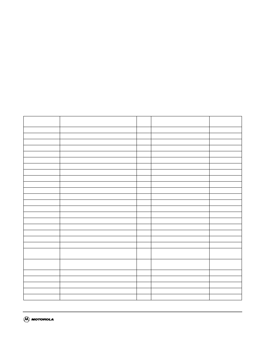
MC9S12A128 Device Guide -- V01.01
49
Section 5 Resets and Interrupts
5.1 Overview
Consult the Exception Processing section of the HCS12 Core User Guide (Motorola document order
number HCS12COREUG/D) for information on resets and interrupts.
5.2 Vectors
5.2.1 Vector Table
Table 5-1
lists interrupt sources and vectors in default order of priority.
Table 5-1 Interrupt Vector Locations
Vector Address
Interrupt Source
CCR
Mask
Local Enable
HPRIO Value
to Elevate
$FFFE, $FFFF
Reset
None
None
≠
$FFFC, $FFFD
Clock Monitor fail reset
None
PLLCTL (CME, SCME)
≠
$FFFA, $FFFB
COP failure reset
None
COP rate select
≠
$FFF8, $FFF9
Unimplemented instruction trap
None
None
≠
$FFF6, $FFF7
SWI
None
None
≠
$FFF4, $FFF5
XIRQ
X-Bit
None
≠
$FFF2, $FFF3
IRQ
I-Bit
IRQCR (IRQEN)
$F2
$FFF0, $FFF1
Real Time Interrupt
I-Bit
CRGINT (RTIE)
$F0
$FFEE, $FFEF
Enhanced Capture Timer channel 0
I-Bit
TIE (C0I)
$EE
$FFEC, $FFED
Enhanced Capture Timer channel 1
I-Bit
TIE (C1I)
$EC
$FFEA, $FFEB
Enhanced Capture Timer channel 2
I-Bit
TIE (C2I)
$EA
$FFE8, $FFE9
Enhanced Capture Timer channel 3
I-Bit
TIE (C3I)
$E8
$FFE6, $FFE7
Enhanced Capture Timer channel 4
I-Bit
TIE (C4I)
$E6
$FFE4, $FFE5
Enhanced Capture Timer channel 5
I-Bit
TIE (C5I)
$E4
$FFE2, $FFE3
Enhanced Capture Timer channel 6
I-Bit
TIE (C6I)
$E2
$FFE0, $FFE1
Enhanced Capture Timer channel 7
I-Bit
TIE (C7I)
$E0
$FFDE, $FFDF
Enhanced Capture Timer overflow
I-Bit
TSRC2 (TOF)
$DE
$FFDC, $FFDD
Pulse accumulator A overflow
I-Bit
PACTL (PAOVI)
$DC
$FFDA, $FFDB
Pulse accumulator input edge
I-Bit
PACTL (PAI)
$DA
$FFD8, $FFD9
SPI0
I-Bit
SP0CR1 (SPIE, SPTIE)
$D8
$FFD6, $FFD7
SCI0
I-Bit
SC0CR2
(TIE, TCIE, RIE, ILIE)
$D6
$FFD4, $FFD5
SCI1
I-Bit
SC1CR2
(TIE, TCIE, RIE, ILIE)
$D4
$FFD2, $FFD3
ATD0
I-Bit
ATD0CTL2 (ASCIE)
$D2
$FFD0, $FFD1
ATD1
I-Bit
ATD1CTL2 (ASCIE)
$D0
$FFCE, $FFCF
Port J
I-Bit
PTJIF (PTJIE)
$CE
$FFCC, $FFCD
Port H
I-Bit
PTHIF(PTHIE)
$CC
$FFCA, $FFCB
Modulus Down Counter underflow
I-Bit
MCCTL(MCZI)
$CA
MC9S12A128 Device Guide -- V01.01
50
5.3 Effects of Reset
When a reset occurs, MCU registers and control bits are changed to known start-up states. Refer to the
respective module Block User Guides for register reset states.
5.3.1 I/O Pins
Refer to the HCS12 Core User Guide (Motorola document order number HCS12COREUG/D) for mode
dependent pin configuration of port A, B, E and K out of reset.
Refer to the MC9S12A128 Port Integration Module (PIM) Block Guide (Motorola document order
number, S12A128PIMV1/D) for reset configurations of all peripheral module ports.
NOTE:
For devices assembled in 80-pin QFP packages all non-bonded out pins should be
configured as outputs after reset in order to avoid current drawn from floating
inputs. Refer to
Table 2-1 Signal Properties
for affected pins.
5.3.2 Memory
Refer to
Table 1-1 Device Memory Map
for locations of the memories depending on the operating
mode after reset.
The RAM array is not automatically initialized out of reset.
$FFC8, $FFC9
Pulse Accumulator B Overflow
I-Bit
PBCTL(PBOVI)
$C8
$FFC6, $FFC7
CRG PLL lock
I-Bit
CRGINT(LOCKIE)
$C6
$FFC4, $FFC5
CRG Self Clock Mode
I-Bit
CRGINT (SCMIE)
$C4
$FFC2, $FFC3
Reserved
$FFC0, $FFC1
IIC Bus
I-Bit
IBCR (IBIE)
$C0
$FFBE, $FFBF
SPI1
I-Bit
SP1CR1 (SPIE, SPTIE)
$BE
$FFBC, $FFBD
Reserved
$FFBA, $FFBB
EEPROM
I-Bit
EECTL(CCIE, CBEIE)
$BA
$FFB8, $FFB9
FLASH
I-Bit
FCTL(CCIE, CBEIE)
$B8
$FF90 to
$FFB7
Reserved
$FF8E, $FF8F
Port P Interrupt
I-Bit
PTPIF (PTPIE)
$8E
$FF8C, $FF8D
PWM Emergency Shutdown
I-Bit
PWMSDN (PWMIE)
$8C
$FF80 to
$FF8B
Reserved

MC9S12A128 Device Guide -- V01.01
51
Section 6 HCS12 Core Block Description
Consult the HCS12 Core User Guide (Motorola document order number HCS12COREUG/D) for
information about the HCS12 core modules, i.e. central processing unit (CPU), interrupt module (INT),
module mapping control module (MMC), multiplexed external bus interface (MEBI), breakpoint module
(BKP) and background debug mode module (BDM).
Section 7 Clock and Reset Generator (CRG) Block
Description
Consult the HCS12 Clock and Reset Generator (CRG) Block Guide (Motorola document order number,
S12CRGV3/D) for information about the Clock and Reset Generator module.
7.1 Device-Specific Information
7.1.1 XCLKS
The XCLKS input signal is active low (see
2.3.13 PE7 / NOACC / XCLKS -- Port E I/O Pin 7
).
Refer to Figure 2-3. Pierce Oscillator Connections (XCLKS=1) of the HCS12 Clock and Reset Generator
(CRG) Block Guide (Motorola document order number, S12CRGV3/D).
Section 8 Enhanced Capture Timer (ECT) Block Description
Consult the HCS12 16-Bit, 8-Channel Enhanced Capture Timer (ECT) Block Guide (Motorola document
order number, S12ECT16B8CV1/D) for information about the Enhanced Capture Timer module.
Section 9 Analog to Digital Converter (ATD) Block
Description
There are two Analog to Digital Converters (ATD1 and ATD0) implemented on the MC9S12A128.
Consult the HCS12 10-Bit, 8-Channel Analog-to-Digital Converter (ATD) Block Guide (Motorola
document order number, S12ATD10B8CV2/D) for information about each Analog to Digital Converter
module.
Section 10 Inter-IC Bus (IIC) Block Description
Consult the HCS12 Inter-Integrated Circuit (IIC) Block Guide (Motorola document order number,
S12IICV2/D) for information about the Inter-IC Bus module.

MC9S12A128 Device Guide -- V01.01
52
Section 11 Serial Communications Interface (SCI) Block
Description
There are two Serial Communications Interfaces (SCI1 and SCI0) implemented on the MC9S12A128
device. Consult the HCS12 Serial Communications Interface (SCI) Block Guide (Motorola document
order number, S12SCIV2/D) for information about each Serial Communications Interface module.
Section 12 Serial Peripheral Interface (SPI) Block
Description
There are two Serial Peripheral Interfaces (SPI1 and SPI0) implemented on MC9S12A128. Consult the
HCS12 Serial Peripheral Interface (SPI) Block Guide (Motorola document order number, S12SPIV2/D)
for information about each Serial Peripheral Interface module.
Section 13 Pulse Width Modulator (PWM) Block Description
Consult the HCS12 8-Bit, 8-Channel Pulse Width Modulator (PWM) Block Guide (Motorola document
order number, S12PWM8B8CV1/D) for information about the Pulse Width Modulator module.
Section 14 Flash EEPROM 128K Block Description
Consult the HCS12 128K FLASH Block Guide (Motorola document order number, S12FTS128KV1/D) for
information about the flash module.
Section 15 EEPROM 2K Block Description
Consult the HCS12 2K EEPROM Block Guide (Motorola document order number, S12EETS2KV1/D) for
information about the EEPROM module.
Section 16 RAM Block Description
This module supports single-cycle misaligned word accesses.

MC9S12A128 Device Guide -- V01.01
53
Section 17 Port Integration Module (PIM) Block Description
Consult the MC9S12A128 Port Integration Module (PIM) Block Guide (Motorola document order
number, S12A128PIMV1/D) for information about the Port Integration Module.
Section 18 Voltage Regulator (V
REG
) Block Description
Consult the HCS12 Voltage Regulator Block Guide (Motorola document order number, S12VREGV1/D)
for information about the dual output linear voltage regulator.
Component
Purpose
Type
Value
C1
V
DD1
filter cap
ceramic X7R
100 .. 220nF
C2
V
DD2
filter cap
ceramic X7R
100 .. 220nF
C3
V
DDA
filter cap
ceramic X7R
100nF
C4
V
DDR
filter cap
X7R/tantalum
>=100nF
C5
V
DDPLL
filter cap
ceramic X7R
100nF
C6
V
DDX
filter cap
X7R/tantalum
>=100nF
C7
OSC load cap
C8
OSC load cap
C9
PLL loop filter cap
See
A.5.3 Phase Locked Loop
C10
PLL loop filter cap
C11
DC cutoff cap
R1
PLL loop filter res
Q1
Quartz

MC9S12A128 Device Guide -- V01.01
54
The PCB must be carefully laid out to ensure proper operation of the voltage regulator as well as of the
MCU itself. The following rules must be observed:
∑
Every supply pair must be decoupled by a ceramic capacitor connected as near as possible to the
corresponding pins (C1 - C6).
∑
Central point of the ground star should be the V
SSR
pin.
∑
Use low ohmic low inductance connections between V
SS1
, V
SS2
and V
SSR
.
∑
V
SSPLL
must be directly connected to V
SSR
.
∑
Keep traces of V
SSPLL
, EXTAL and XTAL as short as possible and occupied board area for C7, C8,
C11 and Q1 as small as possible.
∑
Do not place other signals or supplies underneath area occupied by C7, C8, C10 and Q1 and the
connection area to the MCU.
∑
Central power input should be fed in at the V
DDA
/V
SSA
pins.

MC9S12A128 Device Guide -- V01.01
55
Figure 18-1 Recommended PCB Layout 112 LQFP
C5
C4
C1
C6
C3
C2
C8
C7
Q1
C1
0
C9
R1
V
DDX
VSSX
VDDR
VSSR
VDD1
VSS1
VDD2
VSS2
VDDPLL
VSSPLL
VDDA
VSSA
V
R
EG
EN
C1
1
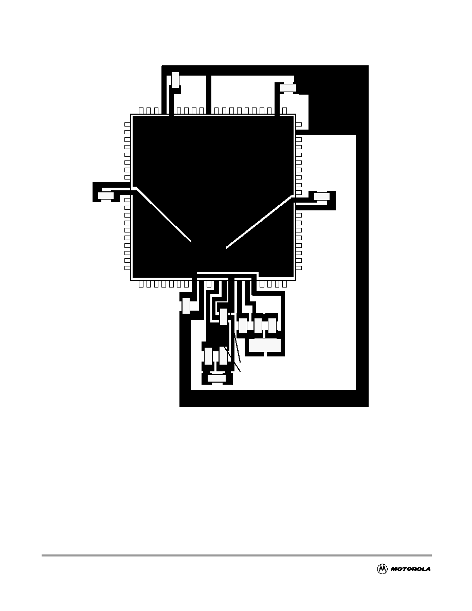
MC9S12A128 Device Guide -- V01.01
56
Figure 18-2 Recommended PCB Layout for 80 QFP
C5
C4
C3
C2
C8
C7
C1
0
C9
R1
C1
1
C6
C1
Q1
VDD1
VSS1
VSS2
VDD2
VSSR
VDDR
VSSPLL
VDDPLL
VDDA
VSSA
VSSX
V
R
EG
EN
VD
DX

MC9S12A128 Device Guide -- V01.01
57
Appendix A Electrical Characteristics
A.1 General
NOTE:
The electrical characteristics given in this section are preliminary and should be
used as a guide only. Values cannot be guaranteed by Motorola and are subject to
change without notice.
This supplement contains the most accurate electrical information for the MC9S12A128 microcontroller
available at the time of publication. The information should be considered PRELIMINARY and is subject
to change.
This introduction is intended to give an overview on several common topics like power supply, current
injection etc.
A.1.1 Parameter Classification
The electrical parameters shown in this supplement are guaranteed by various methods. To give the
customer a better understanding the following classification is used and the parameters are tagged
accordingly in the tables where appropriate.
NOTE:
This classification is shown in the column labeled "C" in the parameter tables
where appropriate.
P:
Those parameters are guaranteed during production testing on each individual device.
C:
Those parameters are achieved by the design characterization by measuring a statistically relevant
sample size across process variations.
T:
Those parameters are achieved by design characterization on a small sample size from typical devices
under typical conditions unless otherwise noted. All values shown in the typical column are within
this category.
D:
Those parameters are derived mainly from simulations.
A.1.2 Power Supply
The MC9S12A128 utilizes several pins to supply power to the I/O ports, A/D converter, oscillator and PLL
as well as the digital core.
The V
DDA
, V
SSA
pair supplies the A/D converter and the resistor ladder of the internal voltage regulator.

MC9S12A128 Device Guide -- V01.01
58
The V
DDX
, V
SSX
, V
DDR
and V
SSR
pairs supply the I/O pins, V
DDR
supplies also the internal voltage
regulator.
V
DD1
, V
SS1
, V
DD2
and V
SS2
are the supply pins for the digital logic, V
DDPLL
, V
SSPLL
supply the oscillator
and the PLL.
V
SS1
and V
SS2
are internally connected by metal.
V
DDA
, V
DDX
, V
DDR
as well as V
SSA
, V
SSX
, V
SSR
are connected by anti-parallel diodes for ESD
protection.
NOTE:
In the following context V
DD5
is used for either V
DDA
, V
DDR
and V
DDX
; V
SS5
is used
for either V
SSA
, V
SSR
and V
SSX
unless otherwise noted.
I
DD5
denotes the sum of the currents flowing into the V
DDA
, V
DDX
and V
DDR
pins.
V
DD
is used for V
DD1
, V
DD2
and V
DDPLL
, V
SS
is used for V
SS1
, V
SS2
and V
SSPLL
.
I
DD
is used for the sum of the currents flowing into V
DD1
and V
DD2
.
A.1.3 Pins
There are four groups of functional pins.
A.1.3.1 5V I/O pins
Those I/O pins have a nominal level of 5V. This class of pins is comprised of all port I/O pins, the analog
inputs, BKGD and the RESET pins.The internal structure of all those pins is identical, however some of
the functionality may be disabled. E.g. for the analog inputs the output drivers, pull-up and pull-down
resistors are disabled permanently.
A.1.3.2 Analog Reference
This group is made up by the V
RH
and V
RL
pins.
A.1.3.3 Oscillator
The pins XFC, EXTAL, XTAL dedicated to the oscillator have a nominal 2.5V level. They are supplied
by V
DDPLL
.
A.1.3.4 TEST
This pin is used for production testing only.
A.1.3.5 V
REGEN
This pin is used to enable the on chip voltage regulator.
MC9S12A128 Device Guide -- V01.01
59
A.1.4 Current Injection
Power supply must maintain regulation within operating V
DD5
or V
DD
range during instantaneous and
operating maximum current conditions. If positive injection current (V
in
> V
DD5
) is greater than I
DD5
, the
injection current may flow out of V
DD5
and could result in external power supply going out of regulation.
Ensure external V
DD5
load will shunt current greater than maximum injection current. This will be the
greatest risk when the MCU is not consuming power; e.g. if no system clock is present, or if clock rate is
very low which would reduce overall power consumption.
A.1.5 Absolute Maximum Ratings
Absolute maximum ratings are stress ratings only. A functional operation under or outside those maxima
is not guaranteed. Stress beyond those limits may affect the reliability or cause permanent damage of the
device.
This device contains circuitry protecting against damage due to high static voltage or electrical fields;
however, it is advised that normal precautions be taken to avoid application of any voltages higher than
maximum-rated voltages to this high-impedance circuit. Reliability of operation is enhanced if unused
inputs are tied to an appropriate logic voltage level (e.g., either V
SS5
or V
DD5
).
Table A-1 Absolute Maximum Ratings
(1)
NOTES
:
1. Beyond absolute maximum ratings device might be damaged.
Num
Rating
Symbol
Min
Max
Unit
1
I/O, Regulator and Analog Supply Voltage
V
DD5
≠0.3
6.0
V
2
Digital Logic Supply Voltage
(2)
2. The device contains an internal voltage regulator to generate the logic and PLL supply out of the I/O supply. The absolute
maximum ratings apply when the device is powered from an external source.
V
DD
≠0.3
3.0
V
3
PLL Supply Voltage
2
V
DDPLL
≠0.3
3.0
V
4
Voltage difference V
DDX
to V
DDR
and V
DDA
VDDX
≠0.3
0.3
V
5
Voltage difference V
SSX
to V
SSR
and V
SSA
VSSX
≠0.3
0.3
V
6
Digital I/O Input Voltage
V
IN
≠0.3
6.0
V
7
Analog Reference
V
RH,
V
RL
≠0.3
6.0
V
8
XFC, EXTAL, XTAL inputs
V
ILV
≠0.3
3.0
V
9
TEST input
V
TEST
≠0.3
10.0
V
10
Instantaneous Maximum Current
Single pin limit for all digital I/O pins
(3)
3. All digital I/O pins are internally clamped to V
SSX
and V
DDX
, V
SSR
and V
DDR
or V
SSA
and V
DDA
.
I
D
≠25
+25
mA
11
Instantaneous Maximum Current
Single pin limit for XFC, EXTAL, XTAL
(4)
4. Those pins are internally clamped to V
SSPLL
and V
DDPLL
.
I
DL
≠25
+25
mA
12
Instantaneous Maximum Current
Single pin limit for TEST
(5)
5. This pin is clamped low to V
SSPLL
, but not clamped high. This pin must be tied low in applications.
I
DT
≠0.25
0
mA
13
Storage Temperature Range
T
stg
≠65
155
∞
C
MC9S12A128 Device Guide -- V01.01
60
A.1.6 ESD Protection and Latch-up Immunity
All ESD testing is in conformity with CDF-AEC-Q100 Stress test qualification for Automotive Grade
Integrated Circuits. During the device qualification ESD stresses were performed for the Human Body
Model (HBM), the Machine Model (MM) and the Charge Device Model.
A device will be defined as a failure if after exposure to ESD pulses the device no longer meets the device
specification. Complete DC parametric and functional testing is performed per the applicable device
specification at room temperature followed by hot temperature, unless specified otherwise in the device
specification.
Table A-2 ESD and Latch-up Test Conditions
Model
Description
Symbol
Value
Unit
Human Body
Series Resistance
R1
1500
Ohm
Storage Capacitance
C
100
pF
Number of Pulse per pin
positive
negative
--
--
3
3
Machine
Series Resistance
R1
0
Ohm
Storage Capacitance
C
200
pF
Number of Pulse per pin
positive
negative
--
--
3
3
Latch-up
Minimum input voltage limit
--
≠2.5
V
Maximum input voltage limit
--
7.5
V
Table A-3 ESD and Latch-Up Protection Characteristics
Num
C
Rating
Symbol
Min
Max
Unit
1
C Human Body Model (HBM)
V
HBM
2000
--
V
2
C Machine Model (MM)
V
MM
200
--
V
3
C Charge Device Model (CDM)
V
CDM
500
--
V
4
C
Latch-up Current at T
A
= 125
∞
C
positive
negative
I
LAT
+100
≠100
--
--
mA
5
C
Latch-up Current at T
A
= 27
∞
C
positive
negative
I
LAT
+200
≠200
--
--
mA
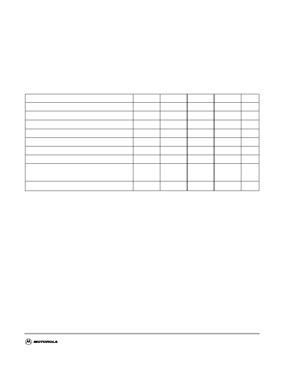
MC9S12A128 Device Guide -- V01.01
61
A.1.7 Operating Conditions
This chapter describes the operating conditions of the device. Unless otherwise noted those conditions
apply to all the following data.
NOTE:
Please refer to the temperature rating of the device (C) with regards to the ambient
temperature T
A
and the junction temperature T
J
. For power dissipation
calculations refer to
A.1.8 Power Dissipation and Thermal Characteristics
.
Table A-4 Operating Conditions
Rating
Symbol
Min
Typ
Max
Unit
I/O, Regulator and Analog Supply Voltage
V
DD5
4.5
5
5.25
V
Digital Logic Supply Voltage
(1)
NOTES
:
1. The device contains an internal voltage regulator to generate the logic and PLL supply out of the I/O supply. The absolute
maximum ratings apply when this regulator is disabled and the device is powered from an external source.
V
DD
2.35
2.5
2.75
V
PLL Supply Voltage
(2)
V
DDPLL
2.25
2.5
2.75
V
Voltage Difference V
DDX
to V
DDR
and V
DDA
VDDX
≠0.1
0
0.1
V
Voltage Difference V
SSX
to V
SSR
and V
SSA
VSSX
≠0.1
0
0.1
V
Oscillator
f
osc
0.5
--
16
MHz
Bus Frequency
f
bus
0.5
--
25
MHz
MC9S12A128C
Operating Junction Temperature Range
T
J
≠40
--
100
∞
C
Operating Ambient Temperature Range
(2)
2. Please refer to
A.1.8 Power Dissipation and Thermal Characteristics
for more details about the relation between
ambient temperature T
A
and device junction temperature T
J
.
T
A
≠40
27
85
∞
C

MC9S12A128 Device Guide -- V01.01
62
A.1.8 Power Dissipation and Thermal Characteristics
Power dissipation and thermal characteristics are closely related. The user must assure that the maximum
operating junction temperature is not exceeded. The average chip-junction temperature (T
J
) in
∞
C can be
obtained from:
The total power dissipation can be calculated from:
Two cases with internal voltage regulator enabled and disabled must be considered:
1.
Internal Voltage Regulator disabled
P
IO
is the sum of all output currents on I/O ports associated with V
DDX
and V
DDR
.
For R
DSON
is valid:
respectively
T
J
T
A
P
D
JA
∑
(
)
+
=
T
J
Junction Temperature, [
∞
C
]
=
T
A
Ambient Temperature, [
∞
C
]
=
P
D
Total Chip Power Dissipation, [W]
=
JA
Package Thermal Resistance, [
∞
C/W]
=
P
D
P
INT
P
IO
+
=
P
INT
Chip Internal Power Dissipation, [W]
=
P
INT
I
DD
V
DD
I
DDPLL
V
DDPLL
I
DDA
+
V
DDA
+
=
P
IO
R
DSON
i
I
IO
i
2
=
R
DSON
V
OL
I
OL
------------ for outputs driven low
;
=
R
DSON
V
DD5
V
OH
≠
I
OH
------------------------------------ for outputs driven high
;
=
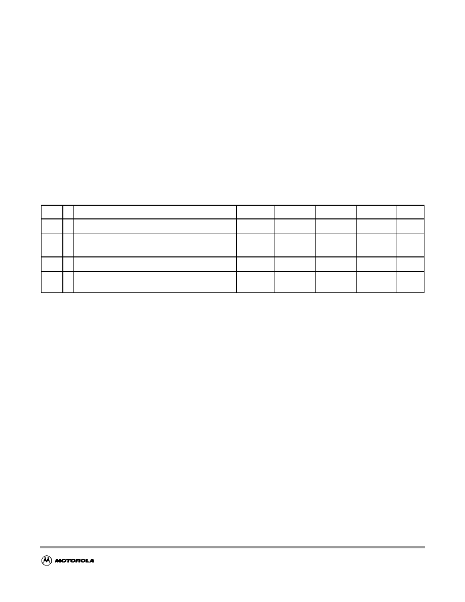
MC9S12A128 Device Guide -- V01.01
63
2.
Internal voltage regulator enabled
I
DDR
is the current shown in
Table A-7
and not the overall current flowing into V
DDR
, which
additionally contains the current flowing into the external loads with output high.
P
IO
is the sum of all output currents on I/O ports associated with V
DDX
and V
DDR
.
Table A-5 Thermal Package Characteristics
(1)
NOTES
:
1. The values for thermal resistance are achieved by package simulations
Num C
Rating
Symbol
Min
Typ
Max
Unit
1
T Thermal Resistance LQFP112, single sided PCB
(2)
2. PC Board according to EIA/JEDEC Standard 51-2
JA
--
--
54
o
C/W
2
T
Thermal Resistance LQFP112, double sided PCB
with 2 internal planes
(3)
3. PC Board according to EIA/JEDEC Standard 51-7
JA
--
--
41
o
C/W
3
T Thermal Resistance LQFP 80, single sided PCB
JA
--
--
51
o
C/W
4
T
Thermal Resistance LQFP 80, double sided PCB
with 2 internal planes
JA
--
--
41
o
C/W
P
INT
I
DDR
V
DDR
I
DDA
V
DDA
+
=
P
IO
R
DSON
i
I
IO
i
2
=
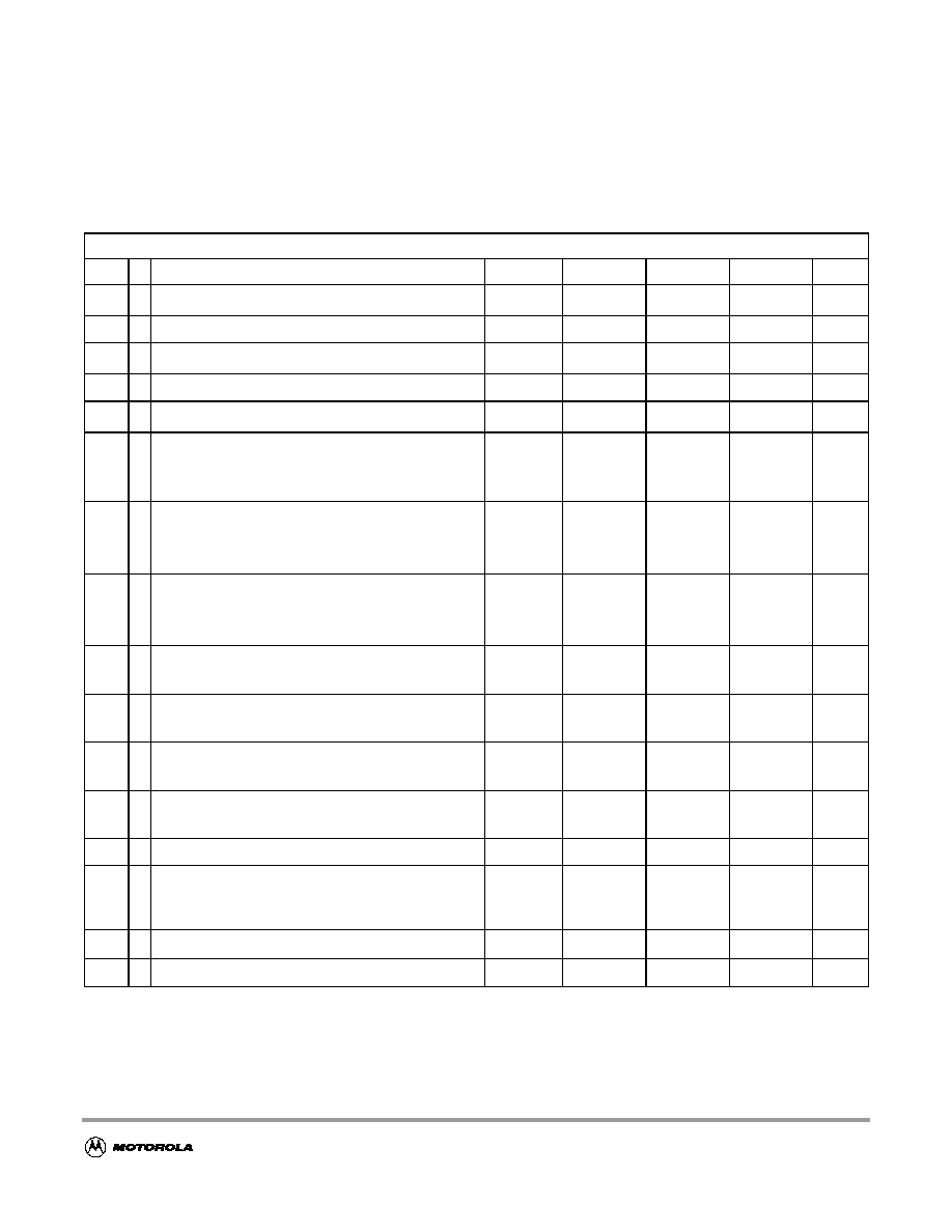
MC9S12A128 Device Guide -- V01.01
64
A.1.9 I/O Characteristics
This section describes the characteristics of all 5V I/O pins. All parameters are not always applicable, e.g.
not all pins feature pull up/down resistances.
Table A-6 5V I/O Characteristics
Conditions are shown in
Table A-4
unless otherwise noted
Num C
Rating
Symbol
Min
Typ
Max
Unit
1
P Input High Voltage
V
IH
0.65*V
DD5
--
--
V
T Input High Voltage
V
IH
--
--
V
DD5
+ 0.3
V
2
P Input Low Voltage
V
IL
--
--
0.35*V
DD5
V
T Input Low Voltage
V
IL
V
SS5
≠ 0.3
--
--
V
3
C Input Hysteresis
V
HYS
--
250
--
mV
4
P
Input Leakage Current (pins in high impedance input
mode)
(1)
V
in
= V
DD5
or V
SS5
NOTES
:
1. Maximum leakage current occurs at maximum operating temperature. Current decreases by approximately one-half for
each 8∞C to 12∞C in the temperature range from 50∞C to 125∞C.
I
in
≠2.5
--
2.5
µ
A
5
P
Output High Voltage (pins in output mode)
Partial Drive
IOH = ≠2.0mA
Full Drive
IOH = ≠10.0mA
V
OH
V
DD5
≠ 0.8
--
--
V
6
P
Output Low Voltage (pins in output mode)
Partial Drive
IOL = +2.0mA
Full Drive
IOL = +10.0mA
V
OL
--
--
0.8
V
7
P
Internal Pull Up Device Current,
tested at V
IL
Max.
I
PUL
--
--
≠130
µ
A
8
P
Internal Pull Up Device Current,
tested at V
IH
Min.
I
PUH
≠10
--
--
µ
A
9
P
Internal Pull Down Device Current,
tested at V
IH
Min.
I
PDH
--
--
130
µ
A
10
P
Internal Pull Down Device Current,
tested at V
IL
Max.
I
PDL
10
--
--
µ
A
11
D Input Capacitance
C
in
--
6
--
pF
12
T
Injection current
(2)
Single Pin limit
Total Device Limit. Sum of all injected currents
2. Refer to
A.1.4 Current Injection
, for more details
I
ICS
I
ICP
≠2.5
≠25
--
2.5
25
mA
13
P Port H, J, P Interrupt Input Pulse filtered
(3)
3. Parameter only applies in STOP or Pseudo STOP mode.
t
PULSE
--
--
3
µ
s
14
P Port H, J, P Interrupt Input Pulse passed
(3)
t
PULSE
10
--
--
µ
s
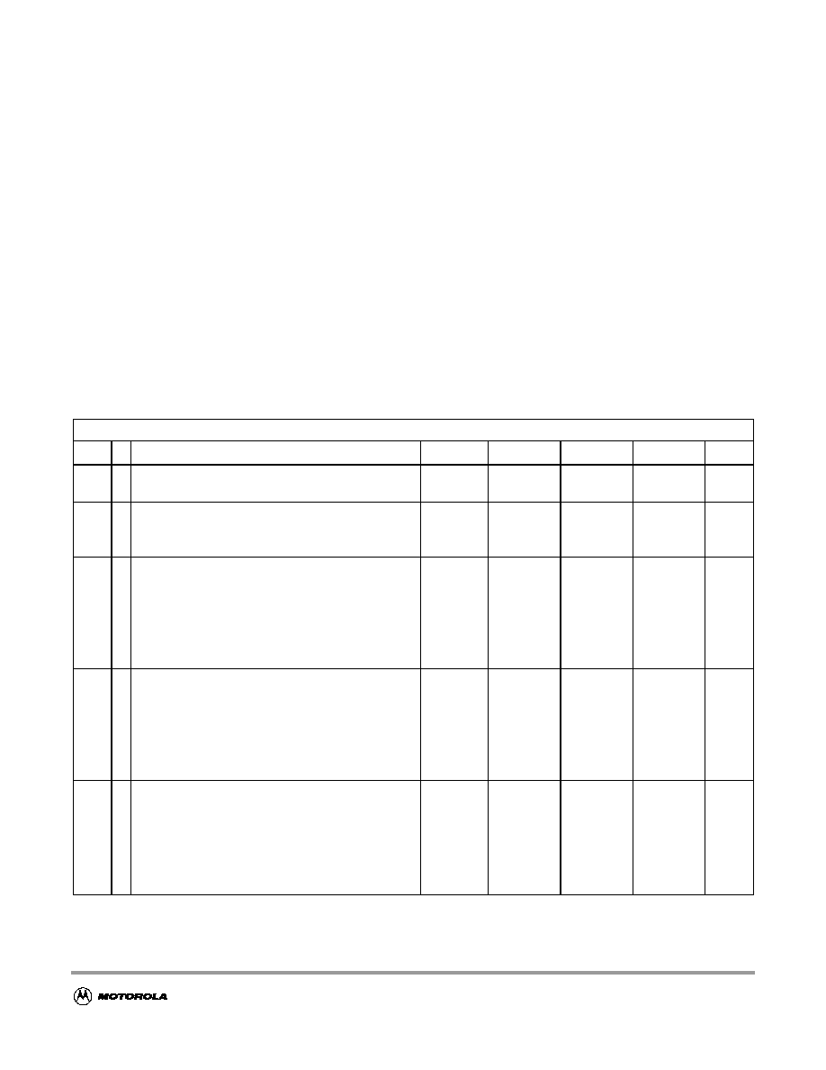
MC9S12A128 Device Guide -- V01.01
65
A.1.10 Supply Currents
This section describes the current consumption characteristics of the device as well as the conditions for
the measurements.
A.1.10.1 Measurement Conditions
All measurements are without output loads. Unless otherwise noted the currents are measured in single
chip mode, internal voltage regulator enabled and at 25MHz bus frequency using a 4MHz oscillator in
Colpitts mode. Production testing is performed using a square wave signal at the EXTAL input.
A.1.10.2 Additional Remarks
In expanded modes the currents flowing in the system are highly dependent on the load at the address, data
and control signals as well as on the duty cycle of those signals. No generally applicable numbers can be
given. A very good estimate is to take the single chip currents and add the currents due to the external
loads.
Table A-7 Supply Current Characteristics
Conditions are shown in
Table A-4
unless otherwise noted
Num C
Rating
Symbol
Min
Typ
Max
Unit
1
P
Run supply currents
Single Chip, Internal regulator enabled
I
DD5
--
--
65
mA
2
P
P
Wait Supply current
All modules enabled, PLL on
only RTI enabled
(1)
I
DDW
--
--
--
--
40
5
mA
3
C
P
C
C
P
C
Pseudo Stop Current (RTI and COP disabled)
(1), (2)
≠40
∞
C
27
∞
C
70
∞
C
85
∞
C
"C" Temp Option 100
∞
C
105
∞
C
NOTES
:
1. PLL off
2. At those low power dissipation levels T
J
= T
A
can be assumed
I
DDPS
--
--
--
--
--
--
370
400
450
550
600
650
500
1600
µ
A
4
C
C
C
C
C
Pseudo Stop Current (RTI and COP enabled)
(1) ,(2)
≠40
∞
C
27
∞
C
70
∞
C
85
∞
C
105
∞
C
I
DDPS
--
--
--
--
--
--
570
600
650
750
850
--
--
--
--
--
--
µ
A
5
C
P
C
C
P
C
Stop Current
(2)
≠40
∞
C
27
∞
C
70
∞
C
85
∞
C
"C" Temp Option 100
∞
C
105
∞
C
I
DDS
--
--
--
--
--
--
12
25
100
130
160
200
100
1200
µ
A
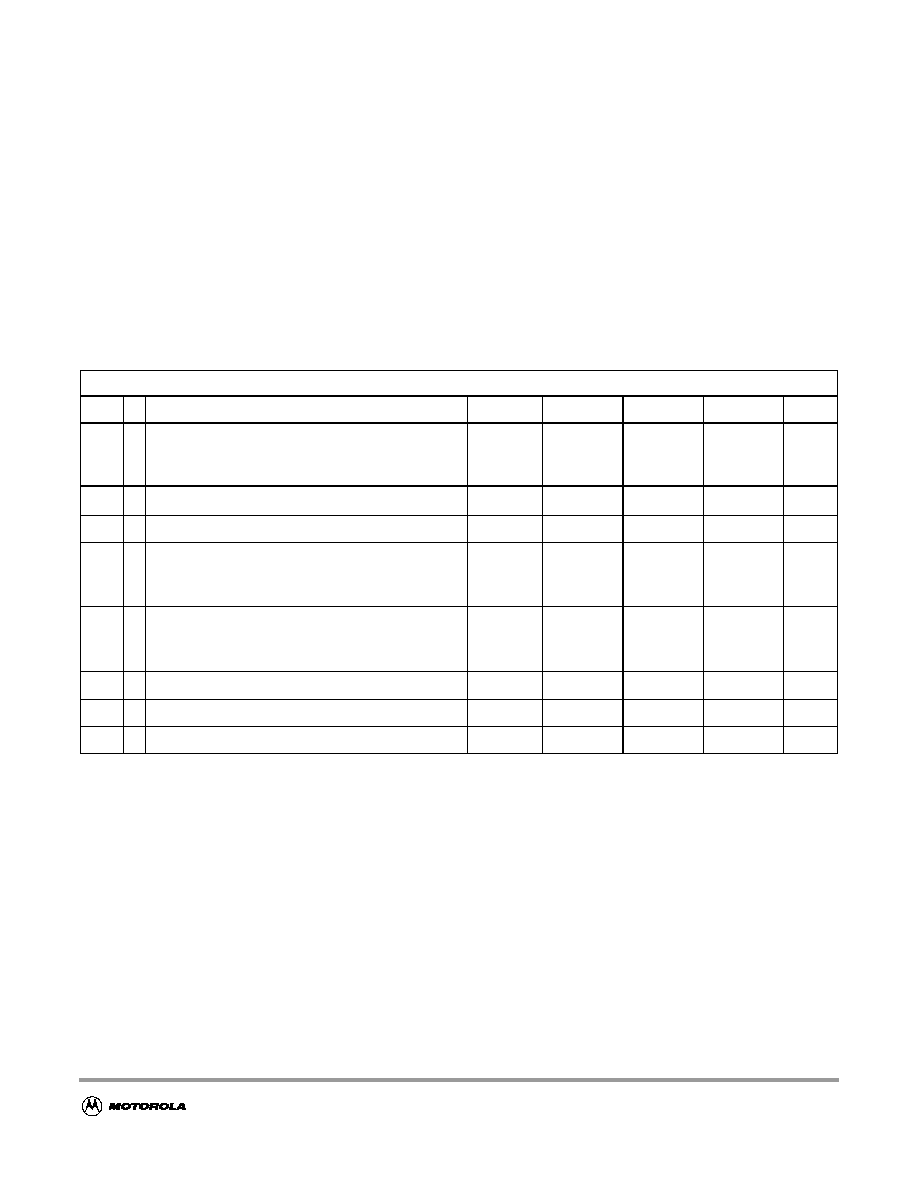
MC9S12A128 Device Guide -- V01.01
66
A.2 ATD Characteristics
This section describes the characteristics of the analog to digital converter.
A.2.1 ATD Operating Characteristics
The
Table A-8
shows conditions under which the ATD operates.
The following constraints exist to obtain full-scale, full range results:
V
SSA
V
RL
V
IN
V
RH
V
DDA
.
This constraint exists since the sample buffer amplifier can not drive
beyond the power supply levels that it ties to. If the input level goes outside of this range it will effectively
be clipped.
A.2.2 Factors Influencing accuracy
Three factors -- source resistance, source capacitance and current injection -- have an influence on the
accuracy of the ATD.
A.2.2.1 Source Resistance
Due to the input pin leakage current as specified in
Table A-6
in conjunction with the source resistance
there will be a voltage drop from the signal source to the ATD input. The maximum source resistance R
S
Table A-8 ATD Operating Characteristics
Conditions are shown in
Table A-4
unless otherwise noted
Num C
Rating
Symbol
Min
Typ
Max
Unit
1
D
Reference Potential
Low
High
V
RL
V
RH
V
SSA
V
DDA
/2
--
--
V
DDA
/2
V
DDA
V
V
2
C Differential Reference Voltage
(1)
NOTES
:
1. Full accuracy is not guaranteed when differential voltage is less than 4.50V
V
RH
≠V
RL
4.50
5.00
5.25
V
3
D ATD Clock Frequency
f
ATDCLK
0.5
--
2.0
MHz
4
D
ATD 10-Bit Conversion Period
Clock Cycles
(2)
Conv, Time at 2.0MHz ATD Clock f
ATDCLK
2. The minimum time assumes a final sample period of 2 ATD clocks cycles while the maximum time assumes a final sample
period of 16 ATD clocks.
N
CONV10
T
CONV10
14
7
--
--
28
14
Cycles
µ
s
5
D
ATD 8-Bit Conversion Period
Clock Cycles
(2)
Conv, Time at 2.0MHz ATD Clock f
ATDCLK
N
CONV8
T
CONV8
12
6
26
13
Cycles
µ
s
6
D Stop Recovery Time (V
DDA
=5.0 Volts)
t
SR
--
--
20
µ
s
7
P Reference Supply current (Both ATD blocks on)
I
REF
--
--
0.750
mA
8
P Reference Supply current (Only one ATD block on)
I
REF
--
--
0.375
mA
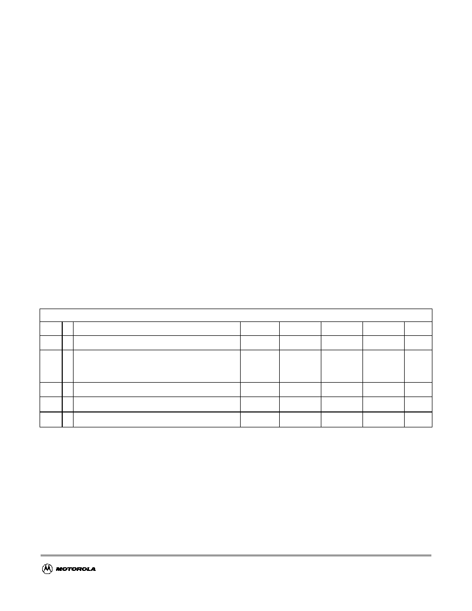
MC9S12A128 Device Guide -- V01.01
67
specifies results in an error of less than 1/2 LSB (2.5mV) at the maximum leakage current. If device or
operating conditions are less than worst case or leakage-induced error is acceptable, larger values of source
resistance is allowed.
A.2.2.2 Source Capacitance
When sampling an additional internal capacitor is switched to the input. This can cause a voltage drop due
to charge sharing with the external and the pin capacitance. For a maximum sampling error of the input
voltage
1LSB, then the external filter capacitor, C
f
1024 * (C
INS
- C
INN
).
A.2.2.3 Current Injection
There are two cases to consider.
1.
A current is injected into the channel being converted. The channel being stressed has conversion
values of $3FF ($FF in 8-bit mode) for analog inputs greater than V
RH
and $000 for values less than
V
RL
unless the current is higher than specified as disruptive condition.
2.
Current is injected into pins in the neighborhood of the channel being converted. A portion of this
current is picked up by the channel (coupling ratio K), This additional current impacts the accuracy
of the conversion depending on the source resistance.
The additional input voltage error on the converted channel can be calculated as V
ERR
= K * R
S
*
I
INJ
, with I
INJ
being the sum of the currents injected into the two pins adjacent to the converted
channel.
Table A-9 ATD Electrical Characteristics
Conditions are shown in
Table A-4
unless otherwise noted
Num C
Rating
Symbol
Min
Typ
Max
Unit
1
C Max input Source Resistance
R
S
--
--
1
K
2
T
Total Input Capacitance
Non Sampling
Sampling
C
INN
C
INS
--
--
--
--
10
22
pF
3
C Disruptive Analog Input Current
I
NA
≠2.5
--
2.5
mA
4
C Coupling Ratio positive current injection
K
p
--
--
10
≠4
A/A
5
C Coupling Ratio negative current injection
K
n
--
--
10
≠2
A/A
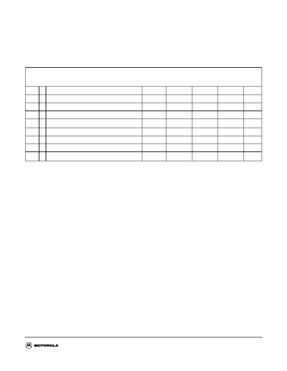
MC9S12A128 Device Guide -- V01.01
68
A.2.3 ATD Accuracy
Table A-10
specifies the ATD conversion performance excluding any errors due to current injection,
input capacitance and source resistance.
For the following definitions see also
Figure A-1
.
Differential Non-Linearity (DNL) is defined as the difference between two adjacent switching steps.
The Integral Non-Linearity (INL) is defined as the sum of all DNLs:
Table A-10 ATD Conversion Performance
Conditions are shown in
Table A-4
unless otherwise noted
V
REF
= V
RH
≠ V
RL
= 5.12V. Resulting to one 8 bit count = 20mV and one 10 bit count = 5mV
f
ATDCLK
= 2.0MHz
Num C
Rating
Symbol
Min
Typ
Max
Unit
1
P 10-Bit Resolution
LSB
--
5
--
mV
2
P 10-Bit Differential Nonlinearity
DNL
≠1
1
Counts
3
P 10-Bit Integral Nonlinearity
INL
≠2.5
±
1.5
2.5
Counts
4
P 10-Bit Absolute Error
(1)
NOTES
:
1. These values include the quantization error which is inherently 1/2 count for any A/D converter.
AE
≠3
±
2.0
3
Counts
5
P 8-Bit Resolution
LSB
--
20
--
mV
6
P 8-Bit Differential Nonlinearity
DNL
≠0.5
--
0.5
Counts
7
P 8-Bit Integral Nonlinearity
INL
≠1.0
±
0.5
1.0
Counts
8
P 8-Bit Absolute Error
(1)
AE
≠1.5
±
1.0
1.5
Counts
DNL i
( )
V
i
V
i
1
≠
≠
1LSB
--------------------------
1
≠
=
INL n
( )
DNL i
( )
i
1
=
n
V
n
V
0
≠
1LSB
---------------------
n
≠
=
=
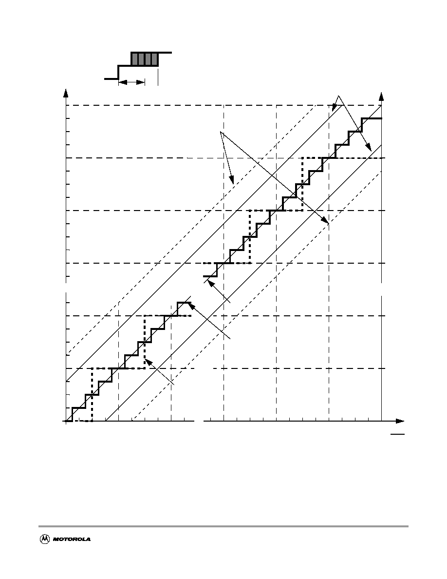
MC9S12A128 Device Guide -- V01.01
69
Figure A-1 ATD Accuracy Definitions
NOTE:
Figure A-1
shows only definitions, for specification values refer to
Table A-10
.
1
5
Vin
mV
10
15
20
25
30
35
40
5085 5090 5095 5100 5105 5110 5115 5120
5065 5070 5075 5080
5060
0
3
2
5
4
7
6
45
$3F7
$3F9
$3F8
$3FB
$3FA
$3FD
$3FC
$3FE
$3FF
$3F4
$3F6
$3F5
8
9
1
2
$FF
$FE
$FD
$3F3
1
0
-B
it R
e
s
o
lut
i
on
8-
B
i
t
R
e
s
o
lution
Ideal Transfer Curve
10-Bit Transfer Curve
8-Bit Transfer Curve
5055
10-Bit Absolute Error Boundary
8-Bit Absolute Error Boundary
LSB
V
i-1
V
i
DNL

MC9S12A128 Device Guide -- V01.01
70
A.3 NVM, Flash, and EEPROM
NOTE:
Unless otherwise noted the abbreviation NVM (Non Volatile Memory) is used for
both Flash and EEPROM.
A.3.1 NVM Timing
The time base for all NVM program or erase operations is derived from the oscillator. A minimum
oscillator frequency f
NVMOSC
is required for performing program or erase operations. The NVM modules
do not have any means to monitor the frequency and will not prevent program or erase operation at
frequencies above or below the specified minimum. Attempting to program or erase the NVM modules at
a lower frequency a full program or erase transition is not assured.
The Flash and EEPROM program and erase operations are timed using a clock derived from the oscillator
using the FCLKDIV and ECLKDIV registers respectively. The frequency of this clock must be set within
the limits specified as f
NVMOP
.
The minimum program and erase times shown in
Table A-11
are calculated for maximum f
NVMOP
and
maximum f
bus
. The maximum times are calculated for minimum f
NVMOP
and a f
bus
of 2MHz.
A.3.1.1 Single Word Programming
The programming time for single word programming is dependant on the bus frequency as a well as on
the frequency f
NVMOP
and can be calculated according to the following formula.
A.3.1.2 Burst Programming
This applies only to the Flash where up to 32 words in a row can be programmed consecutively using burst
programming by keeping the command pipeline filled. The time to program a consecutive word can be
calculated as:
The time to program a whole row is:
Burst programming is more than 2 times faster than single word programming.
t
swpgm
9
1
f
NVMOP
-------------------------
25
1
f
bus
------------
+
=
t
bwpgm
4
1
f
NVMOP
-------------------------
9
1
f
bus
------------
+
=
t
brpgm
t
swpgm
31 t
bwpgm
+
=
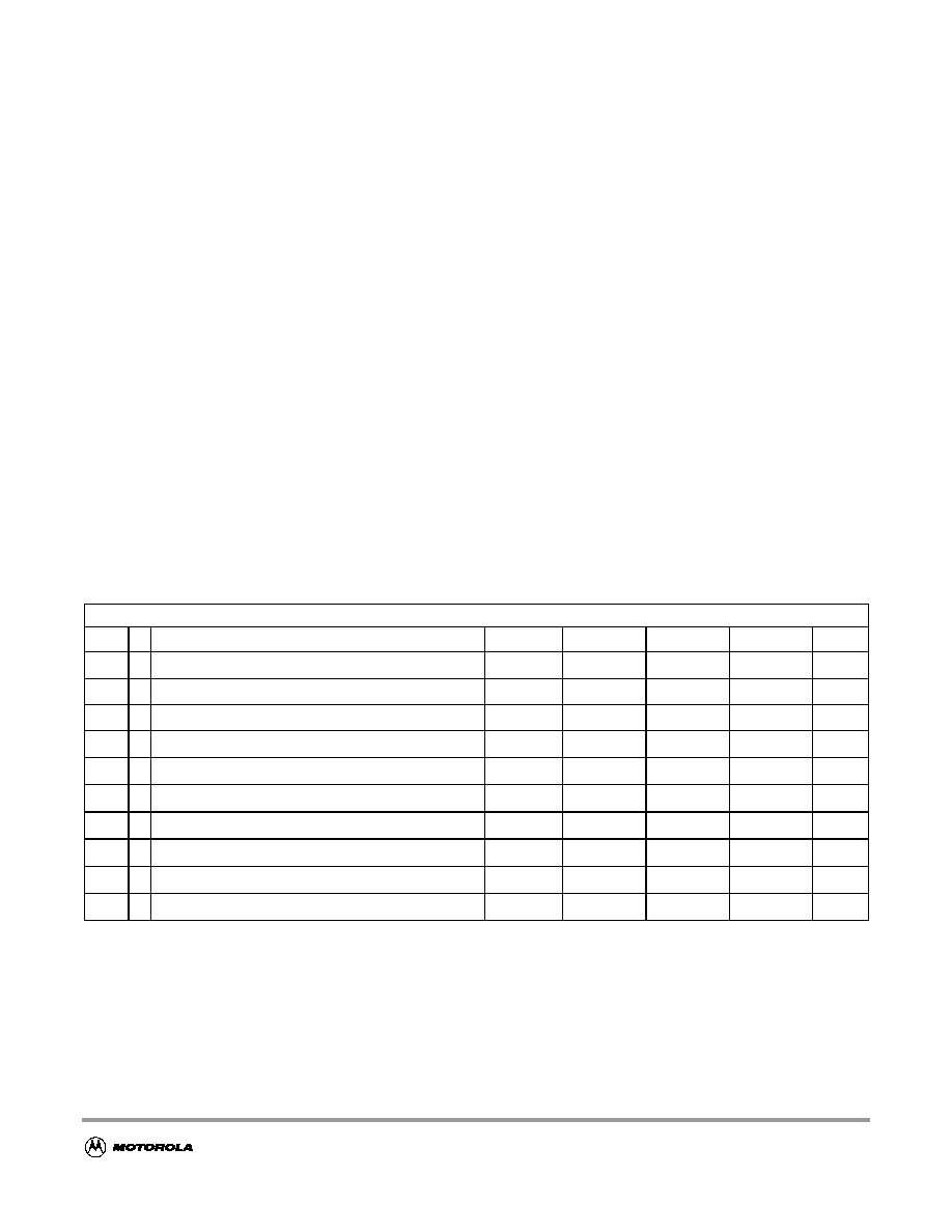
MC9S12A128 Device Guide -- V01.01
71
A.3.1.3 Sector Erase
Erasing a 512 byte Flash sector or a 4 byte EEPROM sector takes:
The setup time can be ignored for this operation.
A.3.1.4 Mass Erase
Erasing a NVM block takes:
The setup time can be ignored for this operation.
A.3.1.5 Blank Check
The time it takes to perform a blank check on the Flash or EEPROM is dependant on the location of the
first non-blank word starting at relative address zero. It takes one bus cycle per word to verify plus a setup
of the command.
Table A-11 NVM Timing Characteristics
Conditions are shown in
Table A-4
unless otherwise noted
Num C
Rating
Symbol
Min
Typ
Max
Unit
1
D External Oscillator Clock
f
NVMOSC
0.5
--
50
(1)
NOTES
:
1. Restrictions for oscillator in crystal mode apply!
MHz
2
D Bus frequency for Programming or Erase Operations
f
NVMBUS
1
--
MHz
3
D Operating Frequency
f
NVMOP
150
--
200
kHz
4
P Single Word Programming Time
t
swpgm
46
(2)
2. Minimum Programming times are achieved under maximum NVM operating frequency f
NVMOP
and maximum bus
frequency f
bus
.
--
74.5
(3)
3. Maximum Erase and Programming times are achieved under particular combinations of f
NVMOP
and bus frequency f
bus
.
Refer to formulae in
A.3.1.1 Single Word Programming
-
A.3.1.4 Mass Erase
for guidance.
µ
s
5
D Flash Burst Programming consecutive word
(4)
4. urst Programming operations are not applicable to EEPROM
t
bwpgm
20.4
(2)
--
31
(3)
µ
s
6
D Flash Burst Programming Time for 32 Words
4
t
brpgm
678.4
(2)
--
1035.5
(3)
µ
s
7
P Sector Erase Time
t
era
20
(5)
5. Minimum Erase times are achieved under maximum NVM operating frequency f
NVMOP
.
--
26.7
(3)
ms
8
P Mass Erase Time
t
mass
100
(5)
--
133
(3)
ms
9
D Blank Check Time Flash per block
t
check
11
(6)
6. Minimum time, if first word in the array is not blank
--
32,778
(7)
7. Maximum time to complete check on an erased block
t
cyc
10
D Blank Check Time EEPROM per block
t
check
11
(6)
--
2058
(7)
t
cyc
t
era
4000
1
f
NVMOP
-------------------------
t
mass
20000
1
f
NVMOP
-------------------------
t
check
location t
cyc
10 t
cyc
+

MC9S12A128 Device Guide -- V01.01
72
A.3.2 NVM Reliability
The reliability of the NVM blocks is guaranteed by stress test during qualification, constant process
monitors and burn-in to screen early life failures.
The failure rates for data retention and program/erase cycling are specified at the operating conditions
noted.
The program/erase cycle count on the sector is incremented every time a sector or mass erase event is
executed.
NOTE:
All values shown in
Table A-12
are target values and subject to further extensive
characterization.
NOTE:
Flash cycling performance is 1000 cycles at ≠40 to +85
∞
C. Data Retention is
specified for 10 years.
NOTE:
EEPROM cycling performance is 10,000 cycles at ≠40 to +85
∞
C. Data retention is
specified for 10 years.
NOTE:
These figures are provided for commercial quality levels not automotive.
Table A-12 NVM Reliability Characteristics
Conditions are shown in
Table A-4
unless otherwise noted
Num
C
NVM Array
Cycles
Data Retention
Lifetime
1
C Flash/EEPROM (≠40 to + 85∞C)
1000
10 years
2
C EEPROM (≠40 to + 85∞C)
10,000
10 years
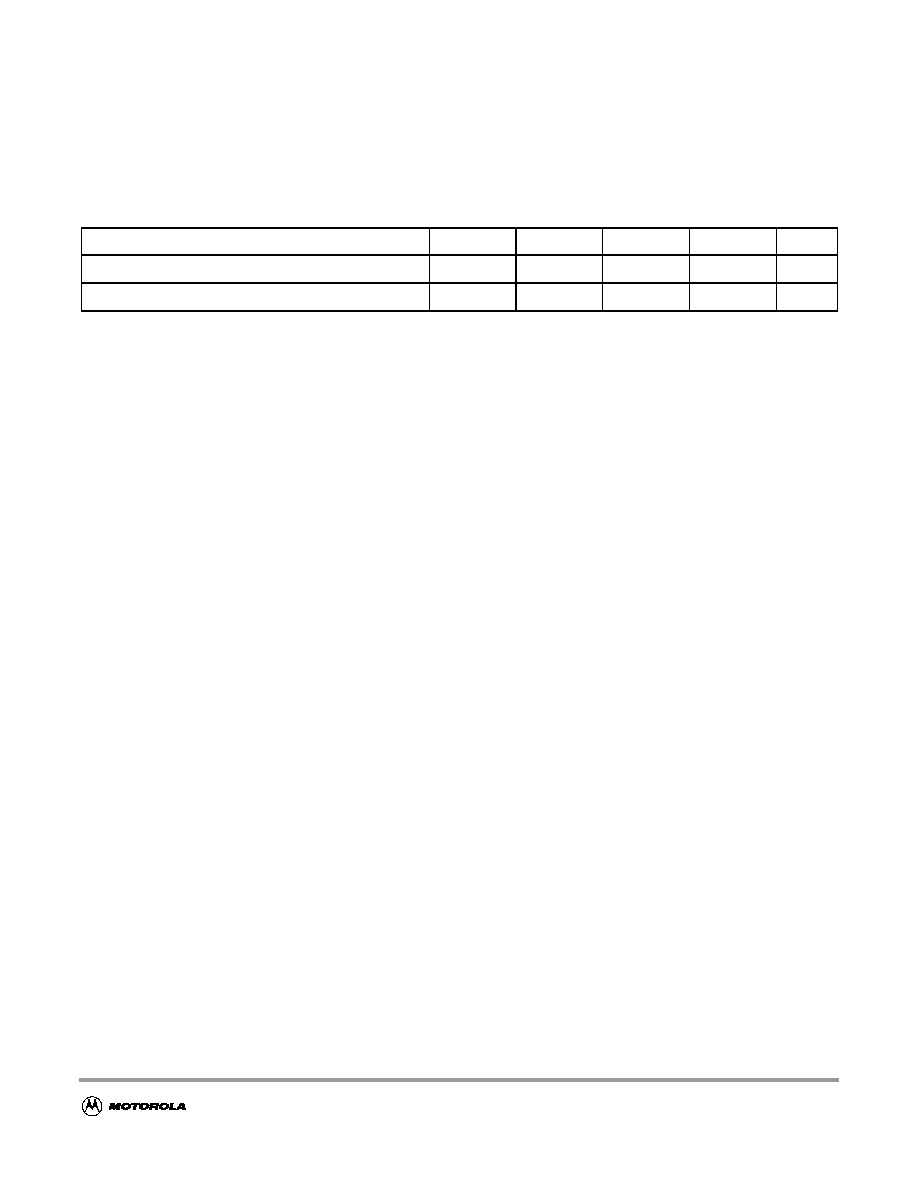
MC9S12A128 Device Guide -- V01.01
73
A.4 Voltage Regulator
The on-chip voltage regulator is intended to supply the internal logic and oscillator circuits. No external
DC load is allowed.
Table A-13 Voltage Regulator Recommended Load Capacitances
Rating
Symbol
Min
Typ
Max
Unit
Load Capacitance on V
DD1, 2
C
LVDD
--
220
--
nF
Load Capacitance on V
DDPLL
C
LVDDPLL
--
220
--
nF
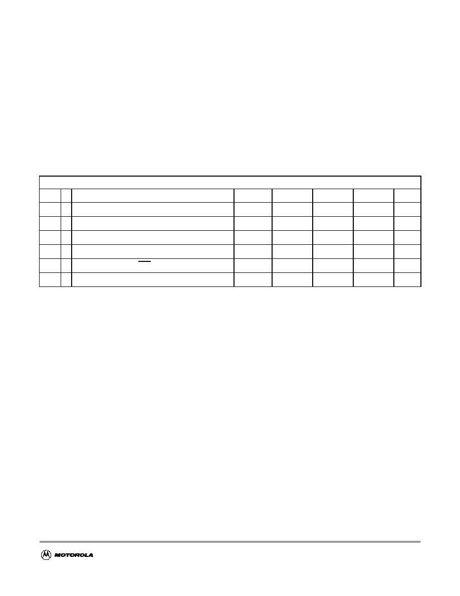
MC9S12A128 Device Guide -- V01.01
74
A.5 Reset, Oscillator and PLL
This section summarizes the electrical characteristics of the various startup scenarios for Oscillator and
Phase-Locked-Loop (PLL).
A.5.1 Startup
Table A-14
summarizes several startup characteristics explained in this section. Detailed description of
the startup behavior can be found in the HCS12 Clock and Reset Generator (CRG) Block Guide (Motorola
document order number, S12CRGV3/D) .
A.5.1.1 POR
The release level V
PORR
and the assert level V
PORA
are derived from the V
DD
supply. They are also valid
if the device is powered externally. After releasing the POR reset the oscillator and the clock quality check
are started. If after a time t
CQOUT
no valid oscillation is detected, the MCU will start using the internal self
clock. The fastest startup time possible is given by n
uposc
.
A.5.1.2 SRAM Data Retention
Provided an appropriate external reset signal is applied to the MCU, preventing the CPU from executing
code when V
DD5
is out of specification limits, the SRAM contents integrity is guaranteed if after the reset
the PORF bit in the CRG Flags Register has not been set.
A.5.1.3 External Reset
When external reset is asserted for a time greater than PW
RSTL
the CRG module generates an internal
reset, and the CPU starts fetching the reset vector without doing a clock quality check, if there was an
oscillation before reset.
Table A-14 Startup Characteristics
Conditions are shown in
Table A-4
unless otherwise noted
Num C
Rating
Symbol
Min
Typ
Max
Unit
1
T POR release level
V
PORR
--
--
2.07
V
2
T POR assert level
V
PORA
0.97
--
--
V
3
D Reset input pulse width, minimum input time
PW
RSTL
2
--
--
t
osc
4
D Startup from Reset
n
RST
192
--
196
n
osc
5
D Interrupt pulse width, IRQ edge-sensitive mode
PW
IRQ
20
--
--
ns
6
D Wait recovery startup time
t
WRS
--
--
14
t
cyc
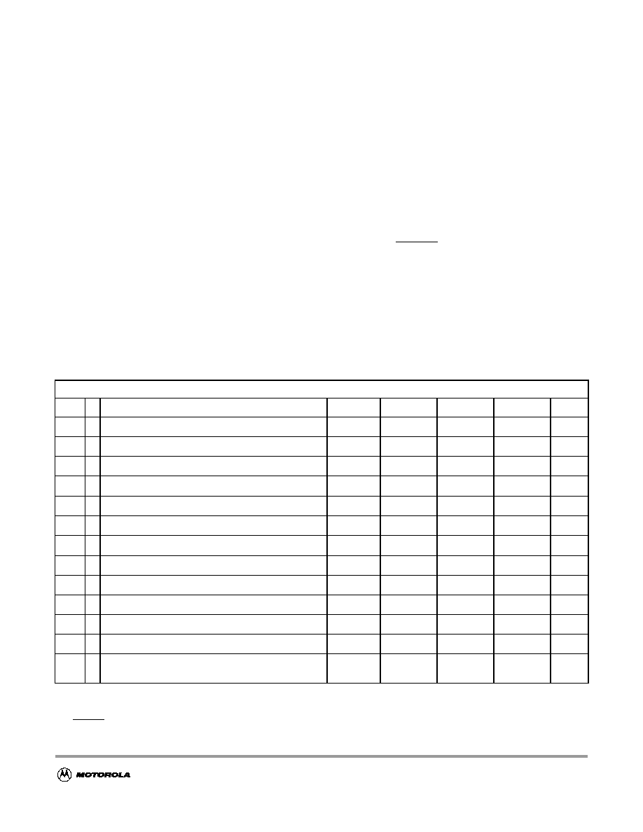
MC9S12A128 Device Guide -- V01.01
75
A.5.1.4 Stop Recovery
Out of STOP the controller can be woken up by an external interrupt. A clock quality check as after POR
is performed before releasing the clocks to the system.
A.5.1.5 Pseudo Stop and Wait Recovery
The recovery from Pseudo STOP and Wait are essentially the same since the oscillator was not stopped in
both modes. The controller can be woken up by internal or external interrupts. After t
wrs
the CPU starts
fetching the interrupt vector.
A.5.2 Oscillator
The device features an internal Colpitts oscillator. By asserting the XCLKS input during reset this
oscillator can be bypassed allowing the input of a square wave. Before asserting the oscillator to the
internal system clocks the quality of the oscillation is checked for each start from either power-on, STOP
or oscillator fail. t
CQOUT
specifies the maximum time before switching to the internal self clock mode after
POR or STOP if a proper oscillation is not detected. The quality check also determines the minimum
oscillator start-up time t
UPOSC
. The device also features a clock monitor. A Clock Monitor Failure is
asserted if the frequency of the incoming clock signal is below the Assert Frequency f
CMFA.
Table A-15 Oscillator Characteristics
Conditions are shown in
Table A-4
unless otherwise noted
Num C
Rating
Symbol
Min
Typ
Max
Unit
1
C Crystal oscillator range
f
OSC
0.5
--
16
MHz
2
P Startup Current
I
OSC
100
--
--
µ
A
3
D Oscillator start-up time from POR or STOP
n
UPOSC
4100
--
--
cyc
OSC
4
C Oscillator start-up time
t
UPOSC
--
8
(1)
NOTES
:
1. f
osc
= 4MHz, C = 22pF.
100
(2)
2. Maximum value is for extreme cases using high Q, low frequency crystals
ms
5
D Clock Quality check time-out
t
CQOUT
0.45
2.5
s
6
P Clock Monitor Failure Assert Frequency
f
CMFA
50
100
200
KHz
7
P External square wave input frequency
(3)
3. XCLKS =0 during reset
f
EXT
0.5
--
50
MHz
8
D External square wave pulse width low
t
EXTL
9.5
--
--
ns
9
D External square wave pulse width high
t
EXTH
9.5
--
--
ns
10
D External square wave rise time
t
EXTR
--
--
1
ns
11
D External square wave fall time
t
EXTF
--
--
1
ns
12
D Input Capacitance (EXTAL, XTAL pins)
C
IN
--
9
--
pF
13
C
DC Operating Bias in Colpitts Configuration on
EXTAL Pin
V
DCBIAS
--
1.1
--
V
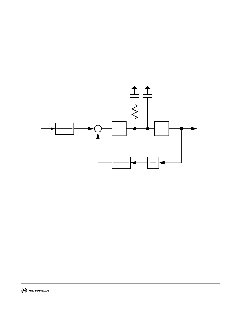
MC9S12A128 Device Guide -- V01.01
76
A.5.3 Phase Locked Loop
The oscillator provides the reference clock for the PLL. The PLL¥s Voltage Controlled Oscillator (VCO)
is also the system clock source in self clock mode.
A.5.3.1 XFC Component Selection
This section describes the selection of the XFC components to achieve a good filter characteristics.
Figure A-2 Basic PLL Functional Diagram
The following procedure can be used to calculate the resistance and capacitance values using typical
values for K
1
, f
1
and i
ch
from
Table A-16
.
The VCO Gain at the desired VCO output frequency is approximated by:
The phase detector relationship is given by:
i
ch
is the current in tracking mode.
f
osc
1
refdv+1
f
ref
Phase
Detector
VCO
K
V
1
synr+1
f
vco
Loop Divider
K
1
2
f
cmp
C
s
R
C
p
V
DDPLL
K
V
K
1
e
f
1
f
vco
≠
(
)
K
1
1V
----------------------------
=
K
i
ch
≠
K
V
=

MC9S12A128 Device Guide -- V01.01
77
The loop bandwidth f
C
should be chosen to fulfill the Gardner's stability criteria by at least a factor of 10,
typical values are 50.
= 0.9 ensures a good transient response.
And finally the frequency relationship is defined as
With the above inputs the resistance can be calculated as:
The capacitance C
s
can now be calculated as:
The capacitance C
p
should be chosen in the range of:
The stabilization delays shown in
Table A-16
are dependant on PLL operational settings and external
component selection (e.g. crystal, XFC filter).
A.5.3.2 Jitter Information
The basic functionality of the PLL is shown in
Figure A-2
. With each transition of the clock f
cmp
, the
deviation from the reference clock f
ref
is measured and input voltage to the VCO is adjusted
accordingly.The adjustment is done continuously with no abrupt changes in the clock output frequency.
Noise, voltage, temperature and other factors cause slight variations in the control loop resulting in a clock
jitter. This jitter affects the real minimum and maximum clock periods as illustrated in
Figure A-3
.
f
C
2
f
ref
1
2
+
+
-------------------------------------------
1
50
------
f
C
f
ref
4 50
--------------
0.9
=
(
)
;
<
<
n
f
VCO
f
ref
---------------
2
synr
1
+
(
)
=
=
R
2
n f
C
K
-----------------------------
=
C
s
2
2
f
C
R
----------------------
0.516
f
C
R
---------------
0.9
=
(
)
;
=
C
s
20
/
C
p
C
s
10
/
MC9S12A128 Device Guide -- V01.01
78
Figure A-3 Jitter Definitions
The relative deviation of t
nom
is at its maximum for one clock period, and decreases towards zero for larger
number of clock periods (N).
Defining the jitter as:
For N < 100, the following equation is a good fit for the maximum jitter:
Figure A-4 Maximum Bus Clock Jitter Approximation
This is very important to notice with respect to timers, serial modules where a pre-scaler will eliminate the
effect of the jitter to a large extent.
2
3
N-1
N
1
0
t
nom
t
max1
t
min1
t
maxN
t
minN
J N
( )
max 1
t
max
N
( )
N t
nom
-----------------------
≠
1
t
min
N
( )
N t
nom
-----------------------
≠
,
=
J N
( )
j
1
N
--------
j
2
+
=
1
5
10
20
N
J(N)
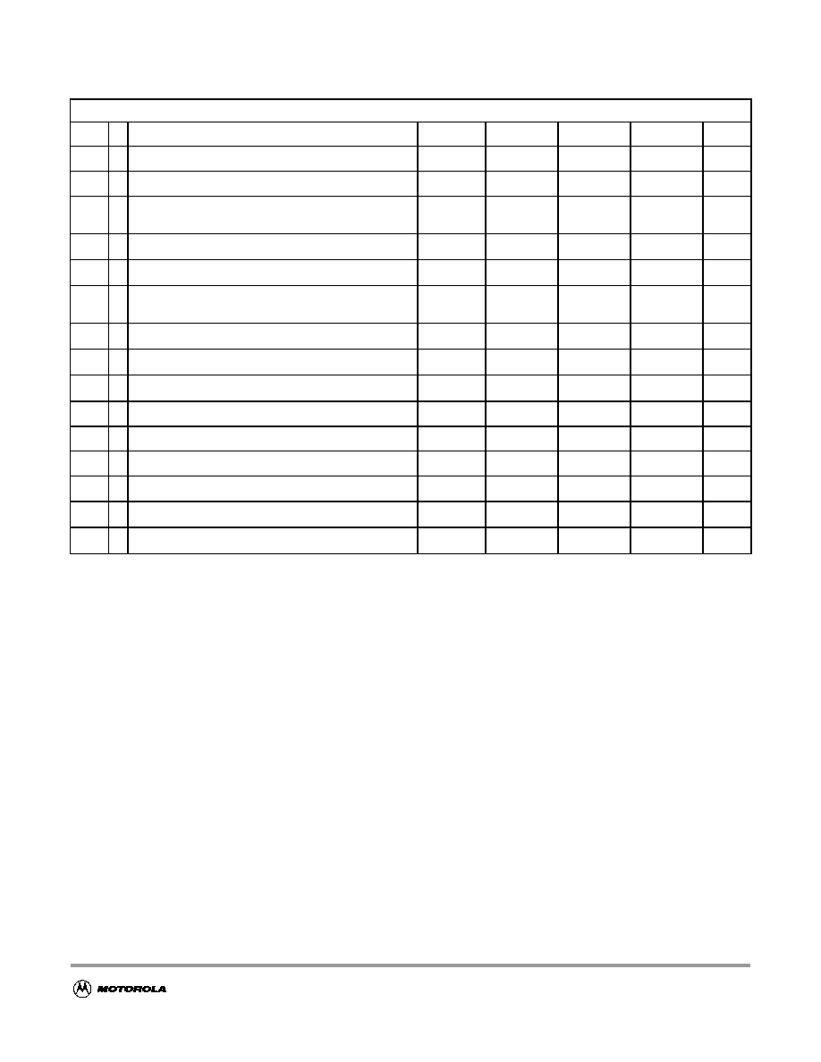
MC9S12A128 Device Guide -- V01.01
79
Table A-16 PLL Characteristics
Conditions are shown in
Table A-4
unless otherwise noted
Num C
Rating
Symbol
Min
Typ
Max
Unit
1
P Self Clock Mode frequency
f
SCM
1
--
5.5
MHz
2
D VCO locking range
f
VCO
8
--
50
MHz
3
D
Lock Detector transition from Acquisition to Tracking
mode
|
trk
|
3
--
4
%
(1)
NOTES
:
1. % deviation from target frequency
4
D Lock Detection
|
Lock
|
0
--
1.5
%
(1)
5
D Un-Lock Detection
|
unl
|
0.5
--
2.5
%
(1)
6
D
Lock Detector transition from Tracking to Acquisition
mode
|
unt
|
6
--
8
%
(1)
7
C PLLON Total Stabilization delay (Auto Mode)
(2)
2. f
REF
= 4MHz, f
BUS
= 25MHz equivalent f
VCO
= 50MHz: REFDV = #$03, SYNR = #$018, Cs = 4.7nF, Cp = 470pF,
Rs = 10K
.
t
stab
--
0.5
--
ms
8
D PLLON Acquisition mode stabilization delay
(2)
t
acq
--
0.3
--
ms
9
D PLLON Tracking mode stabilization delay
(2)
t
al
--
0.2
--
ms
10
D Fitting parameter VCO loop gain
K
1
--
≠120
--
MHz/V
11
D Fitting parameter VCO loop frequency
f
1
--
75
--
MHz
12
D Charge pump current acquisition mode
| i
ch
|
--
38.5
--
µ
A
13
D Charge pump current tracking mode
| i
ch
|
--
3.5
--
µ
A
14
C Jitter fit parameter 1
(2)
j
1
--
--
1.1
%
15
C Jitter fit parameter 2
(2)
j
2
--
--
0.13
%
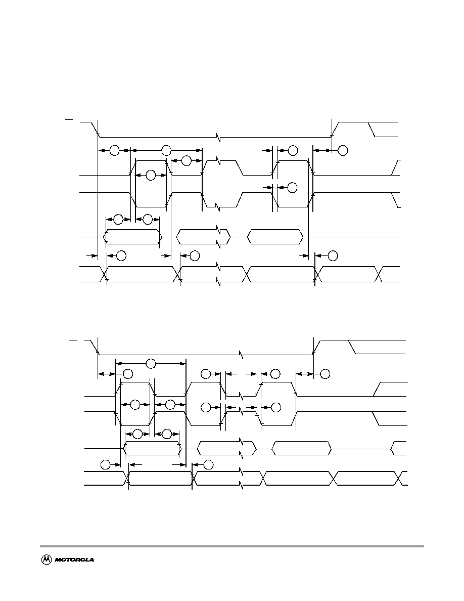
MC9S12A128 Device Guide -- V01.01
80
A.6 SPI
A.6.1 Master Mode
Figure A-5
and
Figure A-6
illustrate the master mode timing. Timing values are shown in
Table A-17
.
Figure A-5 SPI Master Timing (CPHA = 0)
Figure A-6 SPI Master Timing (CPHA =1)
SCK
(OUTPUT)
SCK
(OUTPUT)
MISO
(INPUT)
MOSI
(OUTPUT)
SS
1
(OUTPUT)
1
9
5
6
MSB IN
2
BIT 6 . . . 1
LSB IN
MSB OUT
2
LSB OUT
BIT 6 . . . 1
10
4
4
2
9
(CPOL
=
0)
(CPOL
=
1)
3
11
12
1. If configured as output.
2. LSBF = 0. For LSBF = 1, bit order is LSB, bit 1, ..., bit 6, MSB.
SCK
(OUTPUT)
SCK
(OUTPUT)
MISO
(INPUT)
MOSI
(OUTPUT)
1
5
6
MSB IN
2
BIT 6 . . . 1
LSB IN
MASTER MSB OUT
2
MASTER LSB OUT
BIT 6 . . . 1
4
4
9
11
12
10
PORT DATA
(CPOL
=
0)
(CPOL
=
1)
PORT DATA
SS
1
(OUTPUT)
2
12
11
3
1. If configured as output
2. LSBF = 0. For LSBF = 1, bit order is LSB, bit 1, ..., bit 6, MSB.
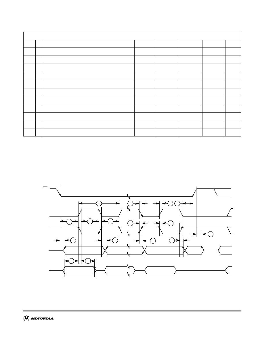
MC9S12A128 Device Guide -- V01.01
81
A.6.2 Slave Mode
Figure A-7
and
Figure A-8
illustrate the slave mode timing. Timing values are shown in
Table A-18
.
Figure A-7 SPI Slave Timing (CPHA = 0)
Table A-17 SPI Master Mode Timing Characteristics
1
NOTES
:
1. The numbers 7, 8 in the column labeled "Num" are missing. This has been done on purpose to be consistent between the
Master and the Slave timing shown in
Table A-18
.
Conditions are shown in
Table A-4
unless otherwise noted, C
LOAD
= 200pF on all outputs
Num C
Rating
Symbol
Min
Typ
Max
Unit
1
P Operating Frequency
f
op
DC
--
1
/
4
f
bus
1
P SCK Period t
sck
= 1./f
op
t
sck
4
--
2048
t
bus
2
D Enable Lead Time
t
lead
1
/
2
--
--
t
sck
3
D Enable Lag Time
t
lag
1
/
2
--
--
t
sck
4
D Clock (SCK) High or Low Time
t
wsck
t
bus
-
30
--
1024 t
bus
ns
5
D Data Setup Time (Inputs)
t
su
25
--
--
ns
6
D Data Hold Time (Inputs)
t
hi
0
--
--
ns
9
D Data Valid (after Enable Edge)
t
v
--
--
25
ns
10
D Data Hold Time (Outputs)
t
ho
0
--
--
ns
11
D Rise Time Inputs and Outputs
t
r
--
--
25
ns
12
D Fall Time Inputs and Outputs
t
f
--
--
25
ns
SCK
(INPUT)
SCK
(INPUT)
MOSI
(INPUT)
MISO
(OUTPUT)
SS
(INPUT)
1
9
5
6
MSB IN
BIT 6 . . . 1
LSB IN
MSB OUT
SLAVE LSB OUT
BIT 6 . . . 1
10
4
4
2
7
(CPOL
=
0)
(CPOL
=
1)
3
12
SLAVE
12
11
10
11
8
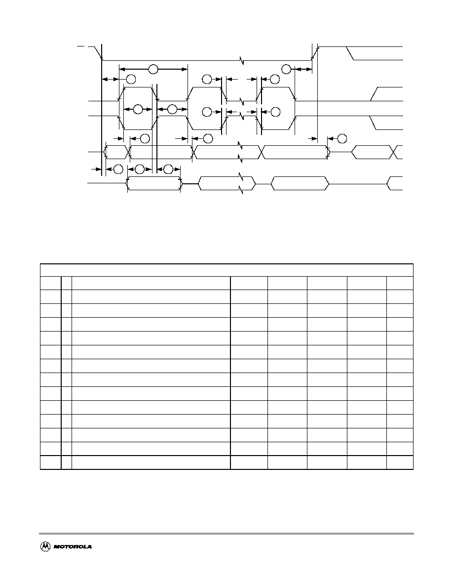
MC9S12A128 Device Guide -- V01.01
82
Figure A-8 SPI Slave Timing (CPHA =1)
Table A-18 SPI Slave Mode Timing Characteristics
Conditions are shown in
Table A-4
unless otherwise noted, CLOAD = 200pF on all outputs
Num C
Rating
Symbol
Min
Typ
Max
Unit
1
P Operating Frequency
f
op
DC
--
1
/
4
f
bus
1
P SCK Period t
sck
= 1./f
op
t
sck
4
--
2048
t
bus
2
D Enable Lead Time
t
lead
1
--
--
t
cyc
3
D Enable Lag Time
t
lag
1
--
--
t
cyc
4
D Clock (SCK) High or Low Time
t
wsck
t
cyc
-
30
--
--
ns
5
D Data Setup Time (Inputs)
t
su
25
--
--
ns
6
D Data Hold Time (Inputs)
t
hi
25
--
--
ns
7
D Slave Access Time
t
a
--
--
1
t
cyc
8
D Slave MISO Disable Time
t
dis
--
--
1
t
cyc
9
D Data Valid (after SCK Edge)
t
v
--
--
25
ns
10
D Data Hold Time (Outputs)
t
ho
0
--
--
ns
11
D Rise Time Inputs and Outputs
t
r
--
--
25
ns
12
D Fall Time Inputs and Outputs
t
f
--
--
25
ns
SCK
(INPUT)
SCK
(INPUT)
MOSI
(INPUT)
MISO
(OUTPUT)
1
5
6
MSB IN
BIT 6 . . . 1
LSB IN
MSB OUT
SLAVE LSB OUT
BIT 6 . . . 1
4
4
9
11
12
10
(CPOL
=
0)
(CPOL
=
1)
SS
(INPUT)
2
12
11
3
SLAVE
7
8

MC9S12A128 Device Guide -- V01.01
83
A.7 External Bus Timing
A timing diagram of the external multiplexed-bus is illustrated in
Figure A-9
with the actual timing
values shown on table
Table A-19
. All major bus signals are included in the diagram. While both a data
write and data read cycle are shown, only one or the other would occur on a particular bus cycle.
A.7.1 General Muxed Bus Timing
The expanded bus timings are highly dependent on the load conditions. The timing parameters shown
assume a balanced load across all outputs.
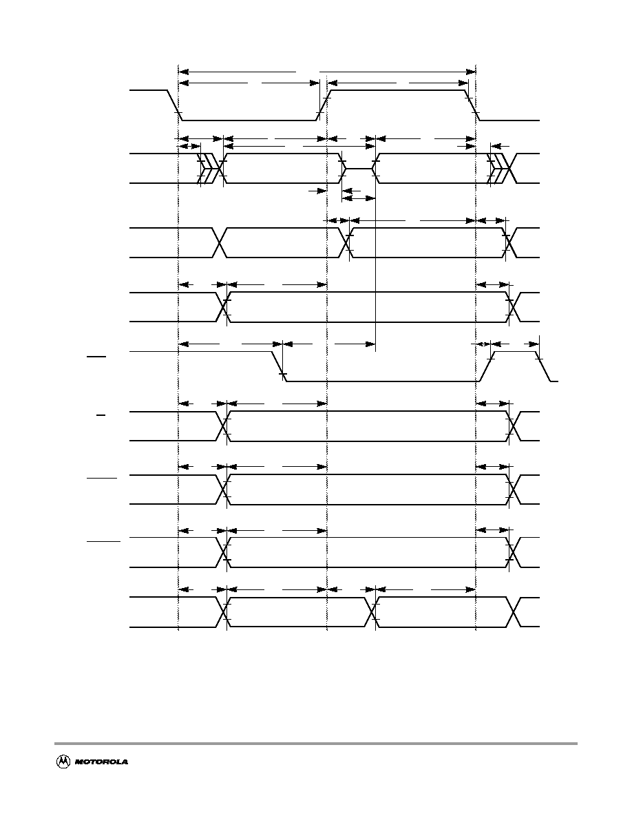
MC9S12A128 Device Guide -- V01.01
84
Figure A-9 General External Bus Timing
Addr/Data
(read)
Addr/Data
(write)
addr
data
data
5
10
11
8
16
6
ECLK
1, 2
3
4
addr
data
data
12
15
9
7
14
13
ECS
21
20
22
23
Non-Multiplexed
17
19
LSTRB
29
NOACC
32
IPIPO0
IPIPO1, PE6,5
35
18
27
28
30
33
36
31
34
R/W
24
26
25
Addresses
PE4
PA, PB
PA, PB
PK5:0
PK7
PE2
PE3
PE7
MC9S12A128 Device Guide -- V01.01
85
Table A-19 Expanded Bus Timing Characteristics
Conditions are shown in
Table A-4
unless otherwise noted, C
LOAD
= 50pF
Num C
Rating
Symbol
Min
Typ
Max
Unit
1
P Frequency of operation (E-clock)
f
o
0
--
25.0
MHz
2
P Cycle time
t
cyc
40
--
--
ns
3
D Pulse width, E low
PW
EL
19
--
--
ns
4
D Pulse width, E high
(1)
PW
EH
19
--
--
ns
5
D Address delay time
t
AD
--
--
8
ns
6
D Address valid time to E rise (PW
EL
≠t
AD
)
t
AV
11
--
--
ns
7
D Muxed address hold time
t
MAH
2
--
--
ns
8
D Address hold to data valid
t
AHDS
7
--
--
ns
9
D Data hold to address
t
DHA
2
--
--
ns
10
D Read data setup time
t
DSR
13
--
--
ns
11
D Read data hold time
t
DHR
0
--
--
ns
12
D Write data delay time
t
DDW
--
--
7
ns
13
D Write data hold time
t
DHW
2
--
--
ns
14
D Write data setup time
(1)
(PW
EH
≠t
DDW
)
t
DSW
12
--
--
ns
15
D Address access time
(1)
(t
cyc
≠t
AD
≠t
DSR
)
t
ACCA
19
--
--
ns
16
D E high access time
(1)
(PW
EH
≠t
DSR
)
t
ACCE
6
--
--
ns
17
D Non-multiplexed address delay time
t
NAD
--
--
6
ns
18
D Non-muxed address valid to E rise (PW
EL
≠t
NAD
)
t
NAV
15
--
--
ns
19
D Non-multiplexed address hold time
t
NAH
2
--
--
ns
20
D Chip select delay time
t
CSD
--
--
16
ns
21
D Chip select access time
(1)
(t
cyc
≠t
CSD
≠t
DSR
)
t
ACCS
11
--
--
ns
22
D Chip select hold time
t
CSH
2
--
--
ns
23
D Chip select negated time
t
CSN
8
--
--
ns
24
D Read/write delay time
t
RWD
--
--
7
ns
25
D Read/write valid time to E rise (PW
EL
≠t
RWD
)
t
RWV
14
--
--
ns
26
D Read/write hold time
t
RWH
2
--
--
ns
27
D Low strobe delay time
t
LSD
--
--
7
ns
28
D Low strobe valid time to E rise (PW
EL
≠t
LSD
)
t
LSV
14
--
--
ns
29
D Low strobe hold time
t
LSH
2
--
--
ns
30
D NOACC strobe delay time
t
NOD
--
--
7
ns
31
D NOACC valid time to E rise (PW
EL
≠t
NOD
)
t
NOV
14
--
--
ns
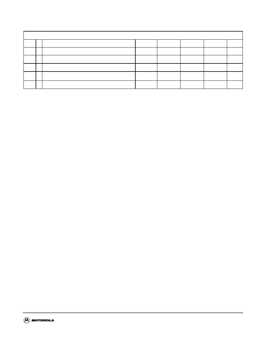
MC9S12A128 Device Guide -- V01.01
86
32
D NOACC hold time
t
NOH
2
--
--
ns
33
D IPIPO[1:0] delay time
t
P0D
2
--
7
ns
34
D IPIPO[1:0] valid time to E rise (PW
EL
≠t
P0D
)
t
P0V
11
--
--
ns
35
D IPIPO[1:0] delay time
1
(PW
EH
-t
P1V
)
t
P1D
2
--
25
ns
36
D IPIPO[1:0] valid time to E fall
t
P1V
11
--
--
ns
NOTES
:
1. Affected by clock stretch: add N x t
cyc
where N=0,1,2 or 3, depending on the number of clock stretches.
Table A-19 Expanded Bus Timing Characteristics
Conditions are shown in
Table A-4
unless otherwise noted, C
LOAD
= 50pF
Num C
Rating
Symbol
Min
Typ
Max
Unit

MC9S12A128 Device Guide -- V01.01
87
Appendix B Package Information
B.1 General
This section provides the physical dimensions of the MC9S12A128 packages.
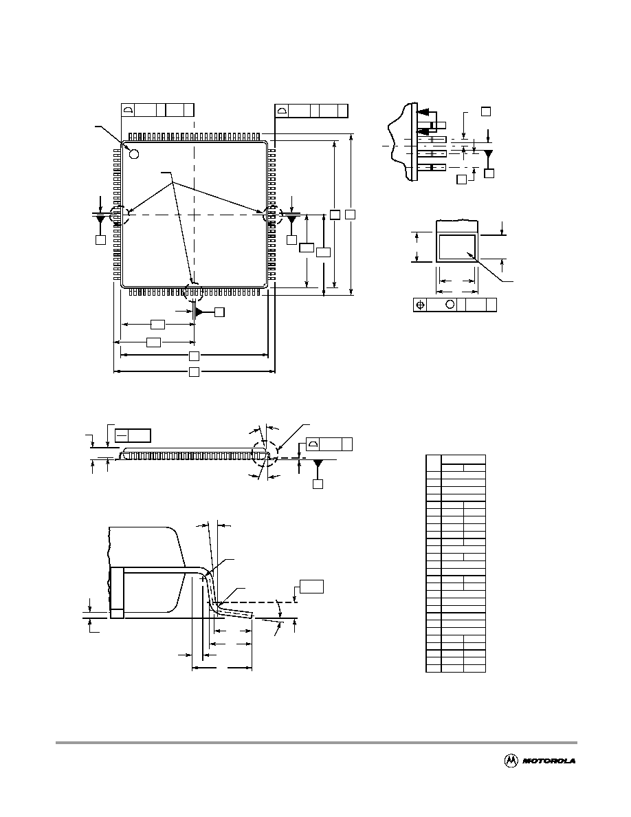
MC9S12A128 Device Guide -- V01.01
88
B.2 112-Pin LQFP Package
Figure B-1 112-Pin LQFP Mechanical Dimensions (Case no. 987)
DIM
A
MIN
MAX
20.000 BSC
MILLIMETERS
A1
10.000 BSC
B
20.000 BSC
B1
10.000 BSC
C
---
1.600
C1
0.050
0.150
C2
1.350
1.450
D
0.270
0.370
E
0.450
0.750
F
0.270
0.330
G
0.650 BSC
J
0.090
0.170
K
0.500 REF
P
0.325 BSC
R1
0.100
0.200
R2
0.100
0.200
S
22.000 BSC
S1
11.000 BSC
V
22.000 BSC
V1
11.000 BSC
Y
0.250 REF
Z
1.000 REF
AA
0.090
0.160
11
∞
11
∞
13
∞
7
∞
13
∞
VIEW Y
L-M
0.20
N
T
4X
4X 28 TIPS
PIN 1
IDENT
1
112
85
84
28
57
29
56
B
V
V1
B1
A1
S1
A
S
VIEW AB
0.10
3
C
C2
2
0.050
SEATING
PLANE
GAGE PLANE
1
VIEW AB
C1
(Z)
(Y)
E
(K)
R2
R1
0.25
J1
VIEW Y
J1
P
G
108X
4X
SECTION J1-J1
BASE
ROTATED 90 COUNTERCLOCKWISE
∞
METAL
J
AA
F
D
L-M
M
0.13
N
T
1
2
3
CL
L-M
0.20
N
T
L
N
M
T
T
112X
X
X=L, M OR N
R
R
NOTES:
1. DIMENSIONING AND TOLERANCING PER
ASME Y14.5M, 1994.
2. DIMENSIONS IN MILLIMETERS.
3. DATUMS L, M AND N TO BE DETERMINED AT
SEATING PLANE, DATUM T.
4. DIMENSIONS S AND V TO BE DETERMINED AT
SEATING PLANE, DATUM T.
5. DIMENSIONS A AND B DO NOT INCLUDE
MOLD PROTRUSION. ALLOWABLE
PROTRUSION IS 0.25 PER SIDE. DIMENSIONS
A AND B INCLUDE MOLD MISMATCH.
6. DIMENSION D DOES NOT INCLUDE DAMBAR
PROTRUSION. ALLOWABLE DAMBAR
PROTRUSION SHALL NOT CAUSE THE D
DIMENSION TO EXCEED 0.46.
8
∞
3
∞
0
∞
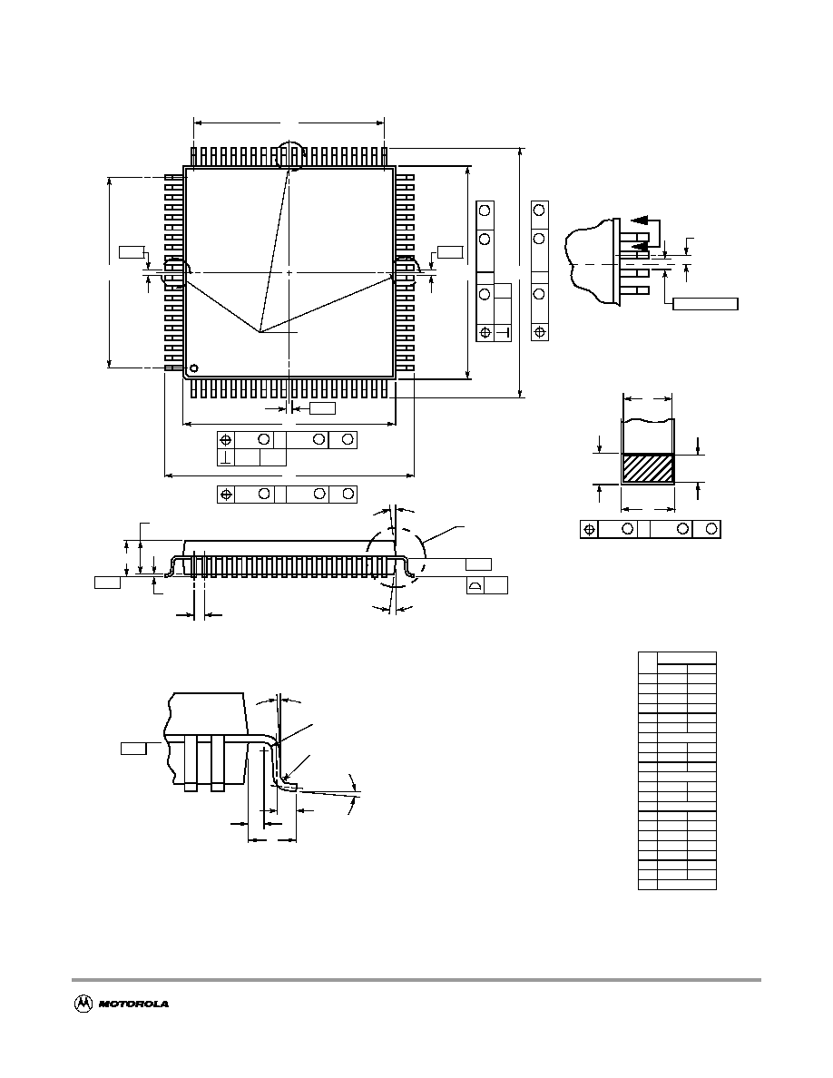
MC9S12A128 Device Guide -- V01.01
89
B.3 80-Pin QFP Package
Figure B-2 80-pin QFP Mechanical Dimensions (Case no. 841B)
NOTES:
1. DIMENSIONING AND TOLERANCING PER
ANSI Y14.5M, 1982.
2. CONTROLLING DIMENSION: MILLIMETER.
3. DATUM PLANE -H- IS LOCATED AT BOTTOM OF
LEAD AND IS COINCIDENT WITH THE
LEAD WHERE THE LEAD EXITS THE PLASTIC
BODY AT THE BOTTOM OF THE PARTING LINE.
4. DATUMS -A-, -B- AND -D- TO BE
DETERMINED AT DATUM PLANE -H-.
5. DIMENSIONS S AND V TO BE DETERMINED
AT SEATING PLANE -C-.
6. DIMENSIONS A AND B DO NOT INCLUDE
MOLD PROTRUSION. ALLOWABLE
PROTRUSION IS 0.25 PER SIDE. DIMENSIONS
A AND B DO INCLUDE MOLD MISMATCH
AND ARE DETERMINED AT DATUM PLANE -H-.
7. DIMENSION D DOES NOT INCLUDE DAMBAR
PROTRUSION. ALLOWABLE DAMBAR
PROTRUSION SHALL BE 0.08 TOTAL IN
EXCESS OF THE D DIMENSION AT MAXIMUM
MATERIAL CONDITION. DAMBAR CANNOT
BE LOCATED ON THE LOWER RADIUS OR
THE FOOT.
SECTION B-B
61
60
DETAIL A
L
41
40
80
-A-
L
-D-
A
S
A-B
M
0.20
D
S
H
0.05
A-B
S
1
20
21
-B-
B
V
J
F
N
D
VIEW ROTATED 90
∞
DETAIL A
B
B
P
-A-,-B-,-D-
E
H
G
M
M
DETAIL C
SEATING
PLANE
-C-
C
DATUM
PLANE
0.10
-H-
DATUM
PLANE
-H-
U
T
R
Q
K
W
X
DETAIL C
DIM
MIN
MAX
MILLIMETERS
A
13.90
14.10
B
13.90
14.10
C
2.15
2.45
D
0.22
0.38
E
2.00
2.40
F
0.22
0.33
G
0.65 BSC
H
---
0.25
J
0.13
0.23
K
0.65
0.95
L
12.35 REF
M
5
10
N
0.13
0.17
P
0.325 BSC
Q
0
7
R
0.13
0.30
S
16.95
17.45
T
0.13
---
U
0
---
V
16.95
17.45
W
0.35
0.45
X
1.6 REF
∞
∞
∞
∞
∞
S
A-B
M
0.20
D
S
C
S
A-B
M
0.
20
D
S
H
0.
05
D
S
A-
B
M
0.
20
D
S
C
S
A-B
M
0.20
D
S
C

MC9S12A128 Device Guide -- V01.01
90

MC9S12A128 Device Guide -- V01.01
91
User Guide End Sheet

MC9S12A128 Device Guide -- V01.01
92
FINAL PAGE OF
92
PAGES