/home/web/htmldatasheet/RUSSIAN/html/motorola/176033

© MOTOROLA 2002
This document contains information on a new product. Specifications and information herein are subject to change without notice.
MOTOROLA
SEMICONDUCTOR
TECHNICAL DATA
MC9S12D-FamilyPP
Rev 6.1, 23-Oct-02
MC9S12D-Family
Product Brief
16-Bit Microcontroller
Designed for automotive multiplexing applications, members of the MC9S12D-Family of 16 bit Flash-
based microcontrollers are fully pin compatible and enable users to choose between different memory
and peripheral options for scalable designs. All MC9S12D-Family members are composed of standard
on-chip peripherals including a 16-bit central processing unit (CPU12), up to 512K bytes of Flash
EEPROM, 14K bytes of RAM, 4K bytes of EEPROM, two asynchronous serial communications
interfaces (SCI), three serial peripheral interfaces (SPI), IIC-bus, an enhanced capture timer (ECT), two
8-channel 10-bit analog-to-digital converters (ADC), an eight-channel pulse-width modulator (PWM),
J1850 interface and up to five CAN 2.0 A, B software compatible modules (MSCAN12). System
resource mapping, clock generation, interrupt control and bus interfacing are managed by the system
integration module (SIM). The MC9S12D-Family has full 16-bit data paths throughout, however, the
external bus can operate in an 8-bit narrow mode so single 8-bit wide memory can be interfaced for
lower cost systems. The inclusion of a PLL circuit allows power consumption and performance to be
adjusted to suit operational requirements. In addition to the I/O ports available in each module, up to 22
I/O ports are available with interrupt capability allowing Wake-Up from STOP or WAIT mode.
Features
NOTE
Not all features listed here are available in all configurations.
Additional information about D and B family inter-operability is given in:
EB386 "HCS12 D-Family Compatibility Considerations" and
EB388 "Using the HCS12 D-Family as a development platform for the HCS12 B family"
· 16-bit CPU12
-- Upward compatible with M68HC11 instruction set
-- Interrupt stacking and programmer's model identical to M68HC11
-- HCS12 Instruction queue
-- Enhanced indexed addressing
· Multiplexed bus
-- Single chip or expanded
-- 16 address/16 data wide or 16 address/8 data narrow modes
-- External address space 1MByte for Data and Program space (112 pin package only)
· Wake-up interrupt inputs depending on the package option
-- 8-bit port H
-- 2-bit port J1:0
-- 2-bit port J7:6 shared with IIC, CAN4 and CAN0 module
-- 8-bit port P shared with PWM or SPI1,2
· Memory options
-- 32K, 64K, 128K, 256K, 512K Byte Flash EEPROM
-- 1K, 2K, 4K Byte EEPROM
-- 2K, 4K, 8K, 12K, 14K Byte RAM

MOTOROLA
MC9S12D-Family
2
PRODUCT PROPOSAL, Rev 6.1, 23-Oct-02
· Analog-to-Digital Converters
-- One or two 8-channel modules with 10-bit resolution depending on the package option
-- External conversion trigger capability
· Up to five 1M bit per second, CAN 2.0 A, B software compatible modules
-- Five receive and three transmit buffers
-- Flexible identifier filter programmable as 2 x 32 bit, 4 x 16 bit or 8 x 8 bit
-- Four separate interrupt channels for Receive, Transmit, Error and Wake-up
-- Low-pass filter wake-up function in STOP mode
-- Loop-back for self test operation
· Enhanced Capture Timer (ECT)
-- 16-bit main counter with 7-bit prescaler
-- 8 programmable input capture or output compare channels; 4 of the 8 input captures with buffer
-- Input capture filters and buffers, three successive captures on four channels, or two captures on four
channels with a capture/compare selectable on the remaining four
-- Four 8-bit or two 16-bit pulse accumulators
-- 16-bit modulus down-counter with 4-bit prescaler
-- Four user-selectable delay counters for signal filtering
· 8 PWM channels with programmable period and duty cycle (7 channels on 80 Pin Packages)
-- 8-bit, 8-channel or 16-bit, 4-channel
-- Separate control for each pulse width and duty cycle
-- Center- or left-aligned outputs
-- Programmable clock select logic with a wide range of frequencies
· Serial interfaces
-- Two asynchronous serial communications interfaces (SCI)
-- Up to three synchronous serial peripheral interfaces (SPI)
-- IIC
· SAE J1850 Compatible Module (BDLC)
-- 10.4 kbps Variable Pulse Width format
-- Byte level receive and transmit
-- 4x receive mode supported
· SIM (System Integration Module)
-- CRG (windowed COP watchdog, real time interrupt, clock monitor, clock generation and reset)
-- MEBI (multiplexed external bus interface)
-- INT (interrupt control)
· Clock generation
-- Phase-locked loop clock frequency multiplier
-- Limp home mode in absence of external clock
-- Clock Monitor
-- Low power 0.5 to 16 MHz crystal oscillator reference clock
· Operating frequency for ambient temperatures T
A
-40°C <= T
A
<= 125°C
-- 50MHz equivalent to 25MHz Bus Speed for single chip
40MHz equivalent to 20MHz Bus Speed in expanded bus modes.
· Internal 5V to 2.5V Regulator
· 112-Pin LQFP or 80-Pin QFP package
-- I/O lines with 5V input and drive capability
-- 5V A/D converter inputs and 5V I/O
-- 2.5V logic supply
· Development support
-- Single-wire background debugTM mode (BDM)
-- On-chip hardware breakpoints
MC9S12D-Family
MOTOROLA
PRODUCT PROPOSAL, Rev 6.1, 23-Oct-02
3
· Pin out explanations:
-- A/D is the number of modules/total number of A/D channels.
-- I/O is the sum of ports capable to act as digital input or output.
112 Pin Packages:
Port A = 8, B = 8, E = 6 + 2 input only, H = 8, J = 4, K = 7, M = 8, P = 8, S = 8, T = 8, PAD = 16 input
only.
22 inputs provide Interrupt capability (H =8, P= 8, J = 4, IRQ, XIRQ)
80 Pin Packages:
Port A = 8, B = 8, E = 6 + 2 input only, J = 2, M = 6, P = 7, S = 4, T = 8, PAD = 8 input only.
11 inputs provide Interrupt capability (P= 7, J = 2, IRQ, XIRQ)
-- CAN0 pins are shared between J1850 pins.
-- CAN0 can be routed under software control from PM1:0 to pins PM3:2 or PM5:4 or PJ7:6.
-- CAN4 pins are shared between IIC pins.
-- CAN4 can be routed under software control from PJ7:6 to pins PM5:4 or PM7:6.
-- Versions with 4 CAN modules will have CAN0, CAN1, CAN2 and CAN4.
-- Versions with 3 CANs modules will have CAN0, CAN1 and CAN4.
-- Versions with 2 CAN modules will have CAN0 and CAN4.
-- Versions with one CAN module will have CAN0.
-- Versions with 2 SPI modules will have SPI0 and SPI1.
-- Versions with 1 SPI will have SPI0.
-- SPI0 can be routed to either Ports PS7:4 or PM5:2.
-- SPI2 pins are shared with PWM7:4; In 112 pin versions SPI2 can be routed under software control to
PH7:4. In 80 pin packages SS-signal of SPI2 is not bonded out!
NOTE
CAN and SPI routing features are not available on the 1st PC9S12DP256 mask set 0K36N!
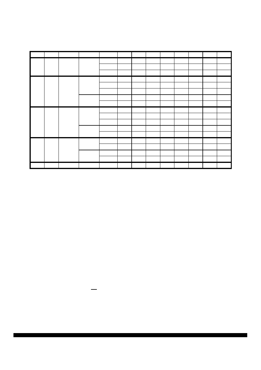
Table 1 List of MC9S12D-Family members
Flash
RAM
EEPROM
Package
Device
CAN
J1850
SCI
SPI
IIC
A/D
PWM
I/O
512K
14K
4K
112LQFP
DP512
5
1
2
3
1
2/16
8
91
DT512
3
0
2
3
1
2/16
8
91
DJ512
2
1
2
3
1
2/16
8
91
256K
12K
4K
112LQFP
DT256
3
0
2
3
1
2/16
8
91
DJ256
2
1
2
3
1
2/16
8
91
DG256
2
0
2
3
1
2/16
8
91
80QFP
DJ256
2
1
2
3
1
1/8
7
59
DG256
2
0
2
3
1
1/8
7
59
128K
8K
2K
112LQFP
DT128
3
0
2
2
1
2/16
8
91
DJ128
2
1
2
2
1
2/16
8
91
DG128
2
0
2
2
1
2/16
8
91
80QFP
DJ128
2
1
2
2
1
1/8
7
59
DG128
2
0
2
2
1
1/8
7
59
64K
4K
1K
112LQFP
DJ64
1
1
2
1
1
2/16
8
91
D64
1
0
2
1
1
2/16
8
91
80QFP
DJ64
1
1
2
1
1
1/8
7
59
D64
1
0
2
1
1
1/8
7
59
32K
2K
1K
80QFP
D32
1
0
2
1
0
1/8
7
59
MOTOROLA
MC9S12D-Family
4
PRODUCT PROPOSAL, Rev 6.1, 23-Oct-02
32K - 512K Byte Flash EEPROM
2K - 14K Byte RAM
Enhanced Capture
RESET
EXTAL
XTAL
VDD1,2
VSS1,2
SCI0
1K - 4K Byte EEPROM
BKGD
R/W
MODB
XIRQ
NOACC/XCLKS
System
Integration
Module
(SIM)
VDDR
CPU12
Periodic Interrupt
COP Watchdog
Clock Monitor
Single-wire Background
Breakpoints
PLL
VSSPLL
XFC
VDDPLL
Multiplexed Address/Data Bus
VDDA
VSSA
VRH
VRL
ATD0
Multiplexed
Wide Bus
Multiplexed
VDDX
VSSX
Internal Logic 2.5V
Narrow Bus
PPAGE
VDDPLL
VSSPLL
PLL 2.5V
IRQ
LSTRB
ECLK
MODA
PA
4
PA
3
PA
2
PA
1
PA
0
PA
7
PA
6
PA
5
TEST
ADDR1
2
ADDR1
1
ADDR1
0
ADDR9
ADDR8
ADDR1
5
ADDR1
4
ADDR1
3
DA
T
A
1
2
DA
T
A
1
1
DA
T
A
1
0
DA
T
A
9
DA
T
A
8
DA
T
A
1
5
DA
T
A
1
4
DA
T
A
1
3
PB4
PB3
PB2
PB1
PB0
PB7
PB6
PB5
ADDR4
ADDR3
ADDR2
ADDR1
ADDR0
ADDR7
ADDR6
ADDR5
DA
T
A
4
DA
T
A
3
DA
T
A
2
DA
T
A
1
DA
T
A
0
DA
T
A
7
DA
T
A
6
DA
T
A
5
DA
T
A
4
DA
T
A
3
DA
T
A
2
DA
T
A
1
DA
T
A
0
DA
T
A
7
DA
T
A
6
DA
T
A
5
PE3
PE4
PE5
PE6
PE7
PE0
PE1
PE2
AN2
AN6
AN0
AN7
AN1
AN3
AN4
AN5
PAD03
PAD04
PAD05
PAD06
PAD07
PAD00
PAD01
PAD02
IOC2
IOC6
IOC0
IOC7
IOC1
IOC3
IOC4
IOC5
PT3
PT4
PT5
PT6
PT7
PT0
PT1
PT2
VRH
VRL
VDDA
VSSA
VRH
VRL
ATD1
AN2
AN6
AN0
AN7
AN1
AN3
AN4
AN5
PAD11
PAD12
PAD13
PAD14
PAD15
PAD08
PAD09
PAD10
VDDA
VSSA
RXD
TXD
MISO
MOSI
PS3
PS4
PS5
PS0
PS1
PS2
SCI1
RXD
TXD
PP3
PP4
PP5
PP6
PP7
PP0
PP1
PP2
PIX2
PIX0
PIX1
PIX3
ECS
PK3
PK7
PK0
PK1
XADDR17
ECS/ROMONE
XADDR14
XADDR15
XADDR16
SCK
SS
PS6
PS7
SPI0
IIC
SDA
SCL
PJ6
PJ7
CAN0
RXCAN
TXCAN
PM1
PM0
CAN1
RXCAN
TXCAN
PM2
PM3
CAN2
RXCAN
TXCAN
PM4
PM5
CAN3
RXCAN
TXCAN
PM6
PM7
KWH2
KWH6
KWH0
KWH7
KWH1
KWH3
KWH4
KWH5
PH3
PH4
PH5
PH6
PH7
PH0
PH1
PH2
KWJ0
KWJ1
PJ0
PJ1
I/O Driver 5V
VDDA
VSSA
A/D Converter 5V &
DDRA
DDRB
PTA
PTB
D
DRE
PT
E
AD
1
AD
0
PT
K
DDRK
PTT
DDRT
PTP
DDRP
PT
S
D
DRS
PT
M
DD
RM
PT
H
D
DRH
PT
J
DDRJ
PK2
BDLC
RXB
TXB
Clock and
Reset
Generation
Module
Voltage Regulator
VSSR
Debug Module
VDD1,2
VSS1,2
VREGEN
VDDR
VSSR
Voltage Regulator 5V & I/O
Not all functionality shown in this
Block diagram is available in all Versions!
CAN4
RXCAN
TXCAN
MISO
MOSI
SCK
SS
SPI2
MISO
MOSI
SCK
SS
SPI1
PIX4
PIX5
PK4
PK5
XADDR18
XADDR19
Voltage Regulator Reference
KWP2
KWP6
KWP0
KWP7
KWP1
KWP3
KWP4
KWP5
KWJ6
KWJ7
Timer
(J1850)
Si
gna
ls s
how
n i
n
Bo
l
d
are
no
t av
aila
ble
on
the
80
Pi
n P
a
ck
age
M
odule t
o
Port
Rout
ing
PWM2
PWM6
PWM0
PWM7
PWM1
PWM3
PWM4
PWM5
PWM
MC9S12D-Family
MOTOROLA
PRODUCT PROPOSAL, Rev 6.1, 23-Oct-02
5
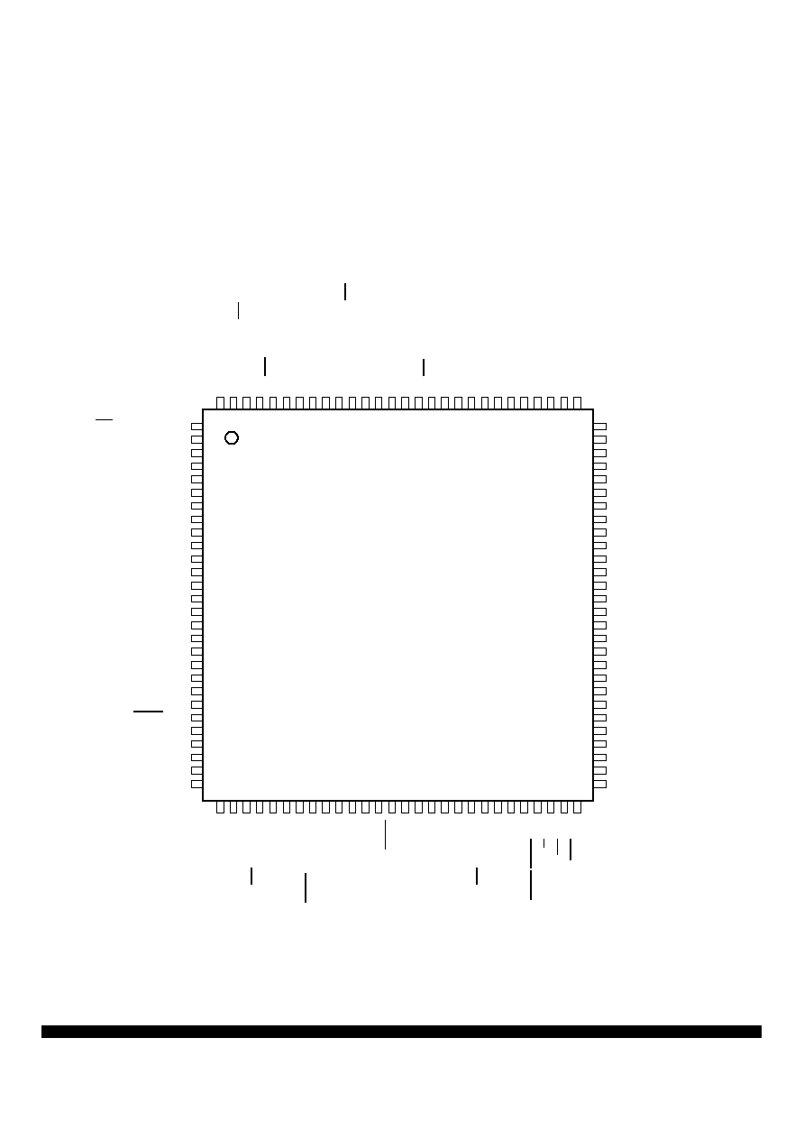
Figure 1 Pin assignments 112 LQFP for MC9S12D-Family
VRH
VDDA
PAD15/AN15/ETRIG1
PAD07/AN07/ETRIG0
PAD14/AN14
PAD06/AN06
PAD13/AN13
PAD05/AN05
PAD12/AN12
PAD04/AN04
PAD11/AN11
PAD03/AN03
PAD10/AN10
PAD02/AN02
PAD09/AN09
PAD01/AN01
PAD08/AN08
PAD00/AN00
VSS2
VDD2
PA7/ADDR15/DATA15
PA6/ADDR14/DATA14
PA5/ADDR13/DATA13
PA4/ADDR12/DATA12
PA3/ADDR11/DATA11
PA2/ADDR10/DATA10
PA1/ADDR9/DATA9
PA0/ADDR8/DATA8
PP
4/K
W
P
4
/P
WM
4/M
I
SO
2
PP
5/K
P
W
5
/P
WM
5/M
O
S
I
2
PP
6/K
W
P
6
/P
WM
6/S
S
2
P
P
7
/
KW
P7
/
P
W
M
7
/
SC
K2
PK
7/E
C
S
/
R
OM
ON
E
VD
DX
VS
SX
PM
0/R
X
C
A
N0
/R
XB
PM
1/T
X
C
A
N0
/TX
B
PM
2/R
X
C
A
N1
/R
XCA
N
0
/
MI
SO
0
PM
3/T
X
C
A
N1
/TX
C
A
N
0
/
SS
0
PM
4/R
X
C
A
N2
/R
XCA
N
0
/
RX
CA
N4/
M
O
S
I0
PM
5/T
X
C
A
N2
/TX
C
A
N
0
/
TX
CAN
4
/S
CK
0
P
J
6/
KW
J
6
/
R
XC
AN
4/
S
D
A
/
RX
CA
N0
P
J
7/
KW
J
7
/
T
XC
AN
4/
S
C
L
/
TX
C
A
N
0
VR
EG
EN
PS
7/S
S
0
PS
6/S
C
K
0
PS
5/M
O
S
I
0
PS
4/M
I
SO
0
PS
3/T
X
D1
PS
2/R
X
D
1
PS
1/T
X
D0
PS
0/R
X
D
0
PM
6/R
X
C
AN3
/R
XCA
N
4
PM
7/T
X
C
AN3
/TX
C
A
N
4
VS
SA
VR
L
SS1/PWM3/KWP3/PP3
SCK1/PWM2/KWP2/PP2
MOSI1/PWM1/KWP1/PP1
MISO1/PWM0/KWP0/PP0
XADDR17/PK3
XADDR16/PK2
XADDR15/PK1
XADDR14/PK0
IOC0/PT0
IOC1/PT1
IOC2/PT2
IOC3/PT3
VDD1
VSS1
IOC4/PT4
IOC5/PT5
IOC6/PT6
IOC7/PT7
XADDR19/PK5
XADDR18/PK4
KWJ1/PJ1
KWJ0/PJ0
MODC/TAGHI/BKGD
ADDR0/DATA0/PB0
ADDR1/DATA1/PB1
ADDR2/DATA2/PB2
ADDR3/DATA3/PB3
ADDR4/DATA4/PB4
A
DDR
5/D
A
T
A
5
/
PB
5
A
DDR
6/D
A
T
A
6
/
PB
6
A
DDR
7/D
A
T
A
7
/
PB
7
SS
2
/KW
H
7
/
PH
7
SC
K2
/KW
H
6
/
PH
6
MO
SI2
/
KW
H5
/PH
5
MIS
O
2
/
KW
H4
/PH
4
XC
LK
S
/N
OA
CC
/PE
7
M
O
D
B
/I
PIP
E
1
/
PE
6
M
O
D
A
/I
PIP
E
0
/
PE
5
EC
LK
/PE
4
VS
SR
VD
DR
RE
SE
T
VDD
P
L
L
XF
C
VSS
PL
L
EX
T
A
L
XT
AL
TE
ST
SS
1
/KW
H
3
/
PH
3
SC
K1
/KW
H
2
/
PH
2
MO
SI1
/
KW
H1
/PH
1
MIS
O
1
/
KW
H0
/PH
0
LS
TR
B
/T
AG
LO
/PE
3
R/
W
/PE
2
IR
Q
/PE
1
XI
RQ
/PE
0
Signals shown in Bold are not available on the 80 Pin Package
MC9S12D-Family
112LQFP
11
2
11
1
11
0
10
9
10
8
10
7
10
6
10
5
10
4
10
3
10
2
10
1
10
0
99
98
97
96
95
94
93
92
91
90
89
88
87
86
85
1
2
3
4
5
6
7
8
9
10
11
12
13
14
15
16
17
18
19
20
21
22
23
24
25
26
27
28
29
30
31
32
33
34
35
36
37
38
39
40
41
42
43
44
45
46
47
48
49
50
51
52
53
54
55
56
84
83
82
81
80
79
78
77
76
75
74
73
72
71
70
69
68
67
66
65
64
63
62
61
60
59
58
57
MOTOROLA
MC9S12D-Family
6
PRODUCT PROPOSAL, Rev 6.1, 23-Oct-02
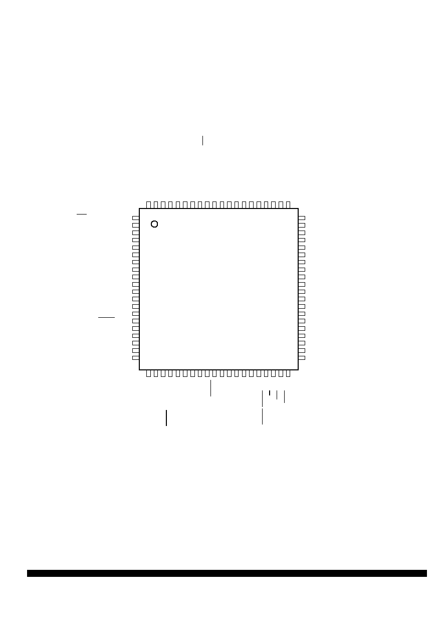
Figure 2 Pin Assignments in 80 QFP for MC9S12D-Family
1
2
3
4
5
6
7
8
9
10
11
12
13
14
15
16
17
18
19
20
80
79
78
77
76
75
74
73
72
71
70
69
68
67
66
65
64
63
62
61
21
22
23
24
25
26
27
28
29
30
31
32
33
34
35
36
37
38
39
40
MC9S12D-Family
80 QFP
VRH
VDDA
PAD07/AN07/ETRIG0
PAD06/AN06
PAD05/AN05
PAD04/AN04
PAD03/AN03
PAD02/AN02
PAD01/AN01
PAD00/AN00
VSS2
VDD2
PA7/ADDR15/DATA15
PA6/ADDR14/DATA14
PA5/ADDR13/DATA13
PA4/ADDR12/DATA12
PA3/ADDR11/DATA11
PA2/ADDR10/DATA10
PA1/ADDR9/DATA9
PA0/ADDR8/DATA8
P
P4/
KW
P4/
PW
M4/
M
IS
O2
P
P5/
KW
P5/
PW
M5/
M
O
S
I2
P
P7/
KW
P7/
PW
M7/
S
C
K
2
V
DDX
V
SSX
P
M
0/
RXC
A
N
0
/R
XB
PM
1
/
T
X
CA
N0
/
T
X
B
P
M
2/
RXC
A
N
1
/R
XC
AN
0/M
I
SO
0
P
M
3/
TXC
A
N
1
/T
XC
AN
0/S
S
0
P
M
4/
RXC
A
N
2
/R
XC
AN
0/R
X
C
A
N4
/M
OSI
0
P
M
5/
TXC
A
N
2
/T
XC
AN
0/TX
CA
N4
/SC
K
0
P
J
6/K
W
J
6
/R
XC
AN
4/S
D
A/
RX
CAN
0
PJ
7
/
KW
J7
/
T
X
C
A
N
4/
SC
L
/
T
X
CA
N0
V
R
EG
EN
P
S3/
TXD
1
P
S2/
RXD
1
P
S1/
TXD
0
P
S0/
RXD
0
V
SSA
VR
L
SS1/PWM3/KWP3/PP3
SCK1/PWM2/KWP2/PP2
MOSI1/PWM1/KWP1/PP1
MISO1/PWM0/KWP0/PP0
IOC0/PT0
IOC1/PT1
IOC2/PT2
IOC3/PT3
VDD1
VSS1
IOC4/PT4
IOC5/PT5
IOC6/PT6
IOC7/PT7
MODC/TAGHI/BKGD
ADDR0/DATA0/PB0
ADDR1/DATA1/PB1
ADDR2/DATA2/PB2
ADDR3/DATA3/PB3
ADDR4/DATA4/PB4
AD
DR
5/D
A
T
A
5/P
B
5
AD
DR
6/D
A
T
A
6/P
B
6
AD
DR
7/D
A
T
A
7/P
B
7
XCL
K
S
/NO
A
C
C
/P
E7
M
O
DB
/IP
IPE
1
/P
E6
M
O
DA
/IP
IPE
0
/P
E5
EC
LK
/
P
E
4
VS
SR
VD
DR
RES
E
T
V
DDP
LL
XF
C
V
SSP
LL
EXT
AL
XT
AL
TE
ST
LS
TRB
/T
A
G
L
O
/P
E3
R/
W
/P
E2
IR
Q
/P
E1
XIR
Q
/P
E0
60
59
58
57
56
55
54
53
52
51
50
49
48
47
46
45
44
43
42
41
MC9S12D-Family
MOTOROLA
PRODUCT PROPOSAL, Rev 6.1, 23-Oct-02
7
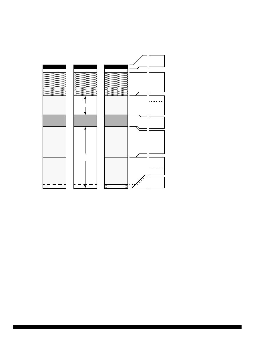
Figure 3 MC9S12Dx512 User Configurable Memory Map
$0000
$FFFF
$C000
$8000
$4000
$0400
$0800
$FF00
EXT
NORMAL
SINGLE CHIP
EXPANDED
SPECIAL
SINGLE CHIP
VECTORS
VECTORS
VECTORS
$FF00
$FFFF
BDM
(If Active)
$C000
$FFFF
16K Fixed Flash EEPROM
2K, 4K, 8K or 16K Protected Boot Sector
$8000
$BFFF
16K Page Window
thirty two * 16K Flash EEPROM Pages
$4000
$6FFF
12K Fixed Flash EEPROM
0.5K, 1K, 2K or 4K Protected Sector
$0800
$3FFF
$7000
$7FFF
4K Bytes EEPROM
Mappable to any 4K Boundary
$0000
$03FF
1K Register Space
Mappable to any 2K Boundary
Mappable to any 16K Boundary
14K Bytes RAM
4K Flash overlapped by EEPROM in this configuration
Alignable to top ($0800 - $3FFF)
or bottom ($0000 - $37FF)
The figure shows a useful map, which is not the map out of reset. After reset the map is:
$0000 - $03FF: Register Space
$0800 - $3FFF: 14K RAM
$0000 - $0FFF: 4K EEPROM (1k $0400 - $07FF visible, $0000 - $03FF and $0800 - $0FFF are not visible)
Various possibilities to make more of the EEPROM fully visible are available, one of them is shown above
EXT
$7000

MOTOROLA
MC9S12D-Family
8
PRODUCT PROPOSAL, Rev 6.1, 23-Oct-02
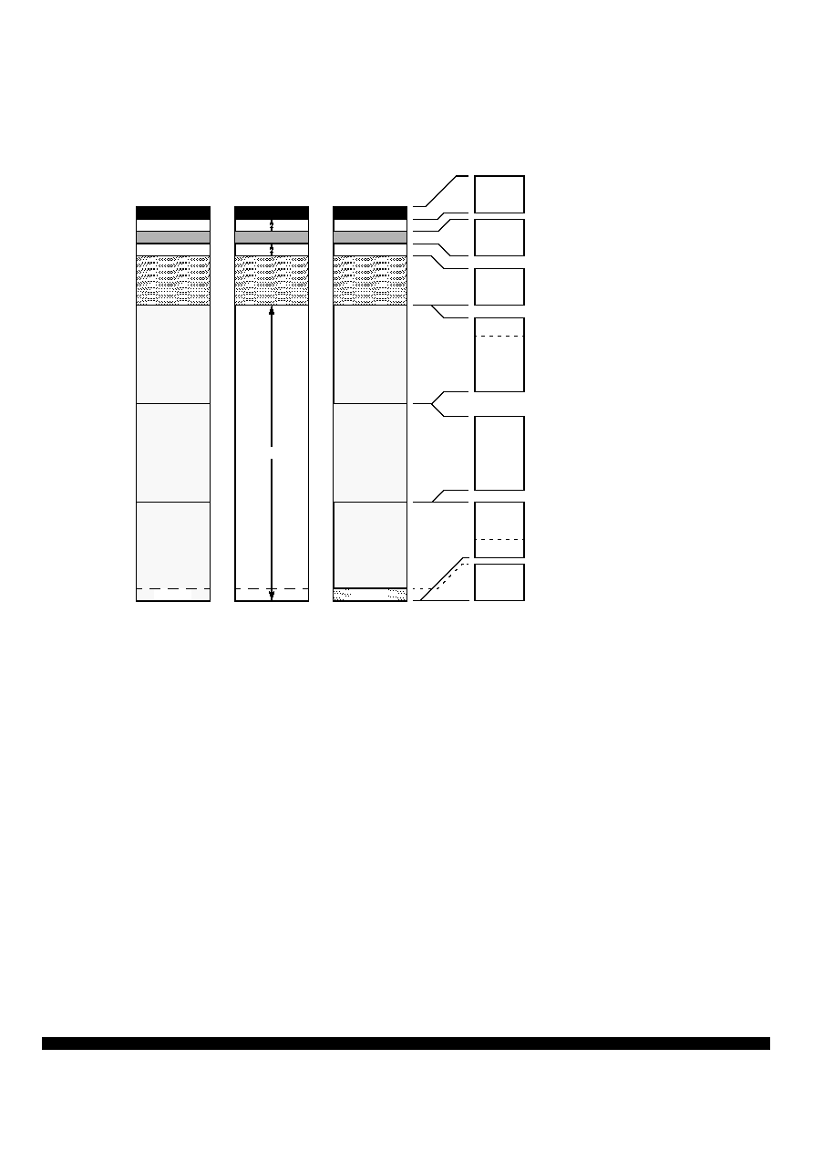
Figure 4 MC9S12Dx256 User Configurable Memory Map
$0000
$FFFF
$C000
$8000
$4000
$0400
$1000
$FF00
EXT
NORMAL
SINGLE CHIP
EXPANDED
SPECIAL
SINGLE CHIP
VECTORS
VECTORS
VECTORS
$FF00
$FFFF
BDM
(If Active)
$C000
$FFFF
16K Fixed Flash EEPROM
2K, 4K, 8K or 16K Protected Boot Sector
$8000
$BFFF
16K Page Window
sixteen * 16K Flash EEPROM Pages
$4000
$7FFF
16K Fixed Flash EEPROM
0.5K, 1K, 2K or 4K Protected Sector
$1000
$3FFF
$0000
$0FFF
4K Bytes EEPROM
Mappable to any 4K Boundary
$0000
$03FF
1K Register Space
Mappable to any 2K Boundary
Mappable to any 16K Boundary
12K Bytes RAM
Initially overlapped by register space
Alignable to top ($1000 - $3FFF)
or bottom ($0000 - $2FFF)
MC9S12D-Family
MOTOROLA
PRODUCT PROPOSAL, Rev 6.1, 23-Oct-02
9
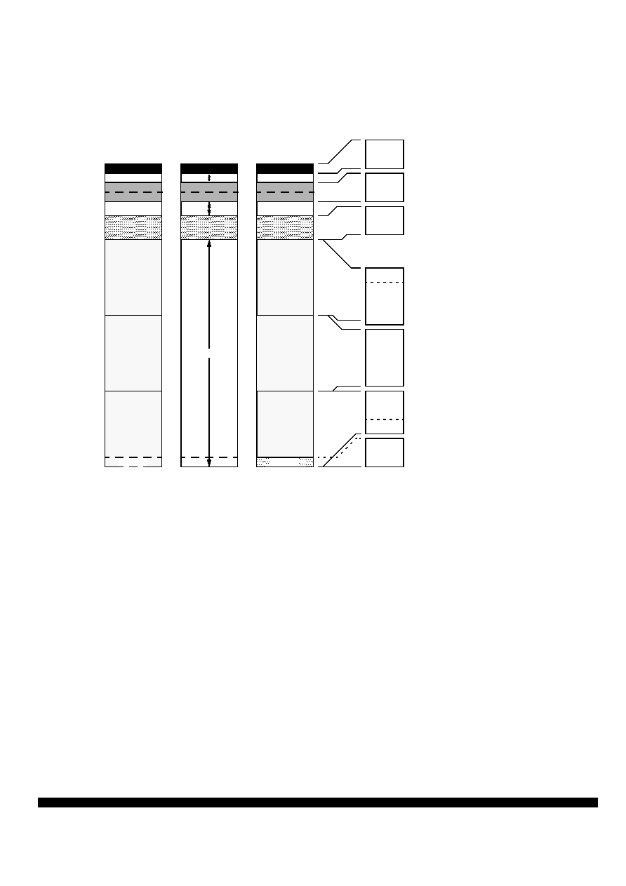
Figure 5 MC9S12Dx128 User Configurable Memory Map
$0000
$FFFF
$C000
$8000
$4000
$0400
$0800
$1000
$2000
$FF00
EXT
NORMAL
SINGLE CHIP
EXPANDED
SPECIAL
SINGLE CHIP
VECTORS
VECTORS
VECTORS
$FF00
$FFFF
BDM
(If Active)
$C000
$FFFF
16K Fixed Flash EEPROM
2K, 4K, 8K or 16K Protected Boot Sector
$8000
$BFFF
16K Page Window
eight * 16K Flash EEPROM Pages
$4000
$7FFF
16K Fixed Flash EEPROM
0.5K, 1K, 2K or 4K Protected Sector
$2000
$3FFF
8K Bytes RAM
Mappable to any 8K Boundary
$0800
$0FFF
2K Bytes EEPROM
Mappable to any 2K Boundary
$0000
$03FF
1K Register Space
Mappable to any 2K Boundary
The figure shows a useful map, which is not the map out of reset. After reset the map is:
$0000 - $03FF: Register Space
$0000 - $1FFF: 8K RAM
$0000 - $07FF: 1K EEPROM (not visible)
MOTOROLA
MC9S12D-Family
10
PRODUCT PROPOSAL, Rev 6.1, 23-Oct-02
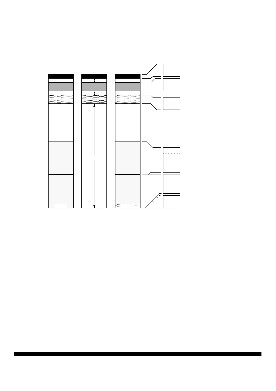
Figure 6 MC9S12Dx64 User Configurable Memory Map
$0000
$FFFF
$C000
$8000
$4000
$0400
$0800
$1000
$3000
$FF00
EXT
NORMAL
SINGLE CHIP
EXPANDED
SPECIAL
SINGLE CHIP
VECTORS
VECTORS
VECTORS
$FF00
$FFFF
BDM
(If Active)
$C000
$FFFF
16K Fixed Flash EEPROM
2K, 4K, 8K or 16K Protected Boot Sector
$8000
$BFFF
16K Page Window
four * 16K Flash EEPROM Pages
$4000
$7FFF
16K Fixed Flash EEPROM
0.5K, 1K, 2K or 4K Protected Sector
$3000
$3FFF
4K Bytes RAM
Mappable to any 4K Boundary
$0800
$0FFF
1K Bytes EEPROM
Mappable to any 2K Boundary
$0000
$03FF
1K Register Space
Mappable to any 2K Boundary
repeated twice in the 2K space
The figure shows a useful map, which is not the map out of reset. After reset the map is:
$0000 - $03FF: Register Space
$0000 - $0FFF: 4K RAM
$0000 - $07FF: 1K EEPROM (not visible)
MC9S12D-Family
MOTOROLA
PRODUCT PROPOSAL, Rev 6.1, 23-Oct-02
11
Figure 7 MC9S12Dx32 User Configurable Memory Map
$0000
$FFFF
$C000
$8000
$0400
$0800
$1000
$4000
$FF00
EXT
NORMAL
SINGLE CHIP
EXPANDED
SPECIAL
SINGLE CHIP
VECTORS
VECTORS
VECTORS
$FF00
$FFFF
BDM
(If Active)
$C000
$FFFF
16K Fixed Flash EEPROM
2K, 4K, 8K or 16K Protected Boot Sector
$8000
$BFFF
16K Fixed Flash EEPROM
two * 16K Flash EEPROM Pages
0.5K, 1K, 2K or 4K Protected Sector
$3800
$3FFF
2K Bytes RAM
Mappable to any 2K Boundary
$0800
$0FFF
1K Bytes EEPROM
Mappable to any 2K Boundary
$0000
$03FF
1K Register Space
Mappable to any 2K Boundary
$3800
Repeated twice in the 2K space
The figure shows a useful map, which is not the map out of reset. After reset the map is:
$0000 - $03FF: Register Space
$0800 - $0FFF: 2K RAM
$0000 - $07FF: 1K EEPROM (not visible)
MOTOROLA
MC9S12D-Family
12
PRODUCT PROPOSAL, Rev 6.1, 23-Oct-02
Figure 8 112-pin LQFP Mechanical Dimensions (case no. 987)
DIM
A
MIN
MAX
20.000 BSC
MILLIMETERS
A1
10.000 BSC
B
20.000 BSC
B1
10.000 BSC
C
---
1.600
C1
0.050
0.150
C2
1.350
1.450
D
0.270
0.370
E
0.450
0.750
F
0.270
0.330
G
0.650 BSC
J
0.090
0.170
K
0.500 REF
P
0.325 BSC
R1
0.100
0.200
R2
0.100
0.200
S
22.000 BSC
S1
11.000 BSC
V
22.000 BSC
V1
11.000 BSC
Y
0.250 REF
Z
1.000 REF
AA
0.090
0.160
11
°
11
°
13
°
7
°
13
°
VIEW Y
L-M
0.20
N
T
4X
4X 28 TIPS
PIN 1
IDENT
1
112
85
84
28
57
29
56
B
V
V1
B1
A1
S1
A
S
VIEW AB
0.10
3
C
C2
2
0.050
SEATING
PLANE
GAGE PLANE
1
VIEW AB
C1
(Z)
(Y)
E
(K)
R2
R1
0.25
J1
VIEW Y
J1
P
G
108X
4X
SECTION J1-J1
BASE
ROTATED 90 COUNTERCLOCKWISE
°
METAL
J
AA
F
D
L-M
M
0.13
N
T
1
2
3
CL
L-M
0.20
N
T
L
N
M
T
T
112X
X
X=L, M OR N
R
R
NOTES:
1. DIMENSIONING AND TOLERANCING PER
ASME Y14.5M, 1994.
2. DIMENSIONS IN MILLIMETERS.
3. DATUMS L, M AND N TO BE DETERMINED AT
SEATING PLANE, DATUM T.
4. DIMENSIONS S AND V TO BE DETERMINED AT
SEATING PLANE, DATUM T.
5. DIMENSIONS A AND B DO NOT INCLUDE
MOLD PROTRUSION. ALLOWABLE
PROTRUSION IS 0.25 PER SIDE. DIMENSIONS
A AND B INCLUDE MOLD MISMATCH.
6. DIMENSION D DOES NOT INCLUDE DAMBAR
8
°
3
°
0
°
MC9S12D-Family
MOTOROLA
PRODUCT PROPOSAL, Rev 6.1, 23-Oct-02
13
Figure 9 80-pin QFP Mechanical Dimensions (case no. 841B)
NOTES:
1. DIMENSIONING AND TOLERANCING PER
ANSI Y14.5M, 1982.
2. CONTROLLING DIMENSION: MILLIMETER.
3. DATUM PLANE -H- IS LOCATED AT BOTTOM OF
LEAD AND IS COINCIDENT WITH THE
LEAD WHERE THE LEAD EXITS THE PLASTIC
BODY AT THE BOTTOM OF THE PARTING LINE.
4. DATUMS -A-, -B- AND -D- TO BE
DETERMINED AT DATUM PLANE -H-.
5. DIMENSIONS S AND V TO BE DETERMINED
AT SEATING PLANE -C-.
6. DIMENSIONS A AND B DO NOT INCLUDE
MOLD PROTRUSION. ALLOWABLE
PROTRUSION IS 0.25 PER SIDE. DIMENSIONS
A AND B DO INCLUDE MOLD MISMATCH
AND ARE DETERMINED AT DATUM PLANE -H-.
7. DIMENSION D DOES NOT INCLUDE DAMBAR
PROTRUSION. ALLOWABLE DAMBAR
PROTRUSION SHALL BE 0.08 TOTAL IN
EXCESS OF THE D DIMENSION AT MAXIMUM
MATERIAL CONDITION. DAMBAR CANNOT
BE LOCATED ON THE LOWER RADIUS OR
THE FOOT.
SECTION B-B
61
60
DETAIL A
L
41
40
80
-A-
L
-D-
A
S
A-B
M
0.20
D
S
H
0.05 A-B
S
1
20
21
-B-
B
V
J
F
N
D
VIEW ROTATED 90
°
DETAIL A
B
B
P
-A-,-B-,-D-
E
H
G
M
M
DETAIL C
SEATING
PLANE
-C-
C
DATUM
PLANE
0.10
-H-
DATUM
PLANE
-H-
U
T
R
Q
K
W
X
DETAIL C
DIM
MIN
MAX
MILLIMETERS
A
13.90
14.10
B
13.90
14.10
C
2.15
2.45
D
0.22
0.38
E
2.00
2.40
F
0.22
0.33
G
0.65 BSC
H
---
0.25
J
0.13
0.23
K
0.65
0.95
L
12.35 REF
M
5
10
N
0.13
0.17
P
0.325 BSC
Q
0
7
R
0.13
0.30
S
16.95
17.45
T
0.13
---
U
0
---
V
16.95
17.45
W
0.35
0.45
X
1.6 REF
°
°
°
°
°
S
A-B
M
0.20
D
S
C
S
A-
B
M
0.
20
D
S
H
0.
0
5
D
S
A-
B
M
0.
2
0
D
S
C
S
A-B
M
0.20
D
S
C

Motorola reserves the right to make changes without further notice to any products herein. Motorola makes no warranty, representation or guarantee regarding
the suitability of its products for any particular purpose, nor does Motorola assume any liability arising out of the application or use of any product or circuit, and
specifically disclaims any and all liability, including without limitation consequential or incidental damages. "Typical" parameters can and do vary in different
applications. All operating parameters, including "Typicals" must be validated for each customer application by customer's technical experts. Motorola does not
convey any license under its patent rights nor the rights of others. Motorola products are not designed, intended, or authorized for use as components in systems
intended for surgical implant into the body, or other applications intended to support or sustain life, or for any other application in which the failure of the Motorola
product could create a situation where personal injury or death may occur. Should Buyer purchase or use Motorola products for any such unintended or
unauthorized application, Buyer shall indemnify and hold Motorola and its officers, employees, subsidiaries, affiliates, and distributors harmless against all
claims, costs, damages, and expenses, and reasonable attorney fees arising out of, directly or indirectly, any claim of personal injury or death associated with
such unintended or unauthorized use, even if such claim alleges that Motorola was negligent regarding the design or manufacture of the part. Motorola
and
are registered trademarks of Motorola, Inc. Motorola, Inc. is an Equal Opportunity/Affirmative Action Employer.
How to reach us:
USA/EUROPE: Motorola Literature Distribution; P.O. Box 5405, Denver, Colorado 80217. 1-303-675-2140
HOME PAGE: http://motorola.com/semiconductors/
JAPAN: Motorola Japan Ltd.; SPS, Technical Information Center, 3-20-1, Minami-Azabu, Minato-ku, Tokyo 106-8573 Japan.
81-3-3440-3569
ASIA/PACIFIC: Motorola Semiconductors H.K. Ltd.; Silicon Harbour Centre, 2 Dai King Street, Tai Po Industrial Estate,
Tai Po, N.T., Hong Kong. 852-266668334
CUSTOMER FOCUS CENTER: 1-800-521-6274
© Motorola, 2002