
MC68HC08JL3/H
Rev. 4
MC68HC08JK1
MC68HRC08JK1
MC68HC08JK3
MC68HRC08JK3
MC68HC08JL3
MC68HRC08JL3
HCMOS Microcontroller Unit
TECHNICAL DATA


MC68H(R)C08JL3
--
Rev. 4
Technical Data
MOTOROLA
List of Sections
3
Technical Data -- MC68H(R)C08JL3
List of Sections
Section 1. General Description . . . . . . . . . . . . . . . . . . . .21
Section 2. Memory . . . . . . . . . . . . . . . . . . . . . . . . . . . . . .27
Section 3. Random-Access Memory (RAM) . . . . . . . . . .37
Section 4. Read-Only Memory (ROM) . . . . . . . . . . . . . . .39
Section 5. Configuration Register (CONFIG) . . . . . . . . .41
Section 6. Central Processor Unit (CPU) . . . . . . . . . . . .45
Section 7. System Integration Module (SIM) . . . . . . . . .65
Section 8. Oscillator (OSC) . . . . . . . . . . . . . . . . . . . . . . .89
Section 9. Monitor ROM (MON) . . . . . . . . . . . . . . . . . . . .95
Section 10. Timer Interface Module (TIM) . . . . . . . . . . .105
Section 11. Analog-to-Digital Converter (ADC) . . . . . .127
Section 12. I/O Ports . . . . . . . . . . . . . . . . . . . . . . . . . . . .137
Section 13. External Interrupt (IRQ) . . . . . . . . . . . . . . .149
Section 14. Keyboard Interrupt Module (KBI). . . . . . . .155
Section 15. Computer Operating Properly (COP) . . . .163
Section 16. Low Voltage Inhibit (LVI) . . . . . . . . . . . . . .169
Section 17. Break Module (BREAK) . . . . . . . . . . . . . . .173
Section 18. Electrical Specifications . . . . . . . . . . . . . . .181
Section 19. Mechanical Specifications . . . . . . . . . . . . .193

List of Sections
Technical Data
MC68H(R)C08JL3
--
Rev. 4
4
List of Sections
MOTOROLA

MC68H(R)C08JL3
--
Rev. 4
Technical Data
MOTOROLA
Table of Contents
5
Technical Data -- MC68H(R)C08JL3
Table of Contents
Section 1. General Description
1.1
Contents . . . . . . . . . . . . . . . . . . . . . . . . . . . . . . . . . . . . . . . . . . 21
1.2
Introduction . . . . . . . . . . . . . . . . . . . . . . . . . . . . . . . . . . . . . . . . 21
1.3
Features . . . . . . . . . . . . . . . . . . . . . . . . . . . . . . . . . . . . . . . . . . 22
1.4
MCU Block Diagram . . . . . . . . . . . . . . . . . . . . . . . . . . . . . . . . . 23
1.5
Pin Assignments . . . . . . . . . . . . . . . . . . . . . . . . . . . . . . . . . . . . 25
1.6
Pin Functions . . . . . . . . . . . . . . . . . . . . . . . . . . . . . . . . . . . . . . 26
Section 2. Memory
2.1
Contents . . . . . . . . . . . . . . . . . . . . . . . . . . . . . . . . . . . . . . . . . . 27
2.2
Introduction . . . . . . . . . . . . . . . . . . . . . . . . . . . . . . . . . . . . . . . . 27
2.3
I/O Section . . . . . . . . . . . . . . . . . . . . . . . . . . . . . . . . . . . . . . . . 29
2.4
Monitor ROM . . . . . . . . . . . . . . . . . . . . . . . . . . . . . . . . . . . . . . 29
Section 3. Random-Access Memory (RAM)
3.1
Contents . . . . . . . . . . . . . . . . . . . . . . . . . . . . . . . . . . . . . . . . . . 37
3.2
Introduction . . . . . . . . . . . . . . . . . . . . . . . . . . . . . . . . . . . . . . . . 37
3.3
Functional Description . . . . . . . . . . . . . . . . . . . . . . . . . . . . . . . 37
Section 4. Read-Only Memory (ROM)
4.1
Contents . . . . . . . . . . . . . . . . . . . . . . . . . . . . . . . . . . . . . . . . . . 39
4.2
Introduction . . . . . . . . . . . . . . . . . . . . . . . . . . . . . . . . . . . . . . . . 39
4.3
Functional Description . . . . . . . . . . . . . . . . . . . . . . . . . . . . . . . 39

Table of Contents
Technical Data
MC68H(R)C08JL3
--
Rev. 4
6
Table of Contents
MOTOROLA
Section 5. Configuration Register (CONFIG)
5.1
Contents . . . . . . . . . . . . . . . . . . . . . . . . . . . . . . . . . . . . . . . . . . 41
5.2
Introduction . . . . . . . . . . . . . . . . . . . . . . . . . . . . . . . . . . . . . . . . 41
5.3
Functional Description . . . . . . . . . . . . . . . . . . . . . . . . . . . . . . . 42
Section 6. Central Processor Unit (CPU)
6.1
Contents . . . . . . . . . . . . . . . . . . . . . . . . . . . . . . . . . . . . . . . . . . 45
6.2
Introduction . . . . . . . . . . . . . . . . . . . . . . . . . . . . . . . . . . . . . . . . 45
6.3
Features . . . . . . . . . . . . . . . . . . . . . . . . . . . . . . . . . . . . . . . . . . 46
6.4
CPU Registers . . . . . . . . . . . . . . . . . . . . . . . . . . . . . . . . . . . . . 46
6.4.1
Accumulator . . . . . . . . . . . . . . . . . . . . . . . . . . . . . . . . . . . . . 47
6.4.2
Index Register . . . . . . . . . . . . . . . . . . . . . . . . . . . . . . . . . . . 48
6.4.3
Stack Pointer . . . . . . . . . . . . . . . . . . . . . . . . . . . . . . . . . . . . 48
6.4.4
Program Counter . . . . . . . . . . . . . . . . . . . . . . . . . . . . . . . . . 49
6.4.5
Condition Code Register . . . . . . . . . . . . . . . . . . . . . . . . . . . 49
6.5
Arithmetic/Logic Unit (ALU) . . . . . . . . . . . . . . . . . . . . . . . . . . . 52
6.6
Low-Power Modes . . . . . . . . . . . . . . . . . . . . . . . . . . . . . . . . . . 52
6.6.1
Wait Mode . . . . . . . . . . . . . . . . . . . . . . . . . . . . . . . . . . . . . . 52
6.6.2
Stop Mode . . . . . . . . . . . . . . . . . . . . . . . . . . . . . . . . . . . . . . 53
6.7
CPU During Break Interrupts . . . . . . . . . . . . . . . . . . . . . . . . . . 53
6.8
Instruction Set Summary . . . . . . . . . . . . . . . . . . . . . . . . . . . . 53
6.9
Opcode Map . . . . . . . . . . . . . . . . . . . . . . . . . . . . . . . . . . . . . . . 53
Section 7. System Integration Module (SIM)
7.1
Contents . . . . . . . . . . . . . . . . . . . . . . . . . . . . . . . . . . . . . . . . . . 65
7.2
Introduction . . . . . . . . . . . . . . . . . . . . . . . . . . . . . . . . . . . . . . . . 66
7.3
SIM Bus Clock Control and Generation . . . . . . . . . . . . . . . . . . 69
7.3.1
Bus Timing . . . . . . . . . . . . . . . . . . . . . . . . . . . . . . . . . . . . . . 69
7.3.2
Clock Start-Up from POR . . . . . . . . . . . . . . . . . . . . . . . . . . . 69
7.3.3
Clocks in Stop Mode and Wait Mode . . . . . . . . . . . . . . . . . . 69

Table of Contents
MC68H(R)C08JL3
--
Rev. 4
Technical Data
MOTOROLA
Table of Contents
7
7.4
Reset and System Initialization. . . . . . . . . . . . . . . . . . . . . . . . . 70
7.4.1
External Pin Reset . . . . . . . . . . . . . . . . . . . . . . . . . . . . . . . . 70
7.4.2
Active Resets from Internal Sources . . . . . . . . . . . . . . . . . . 71
7.4.2.1
Power-On Reset . . . . . . . . . . . . . . . . . . . . . . . . . . . . . . . 72
7.4.2.2
Computer Operating Properly (COP) Reset . . . . . . . . . . 73
7.4.2.3
Illegal Opcode Reset . . . . . . . . . . . . . . . . . . . . . . . . . . . . 73
7.4.2.4
Illegal Address Reset . . . . . . . . . . . . . . . . . . . . . . . . . . . . 73
7.4.2.5
LVI Reset . . . . . . . . . . . . . . . . . . . . . . . . . . . . . . . . . . . . . 74
7.5
SIM Counter . . . . . . . . . . . . . . . . . . . . . . . . . . . . . . . . . . . . . . . 74
7.5.1
SIM Counter During Power-On Reset . . . . . . . . . . . . . . . . . 74
7.5.2
SIM Counter During Stop Mode Recovery . . . . . . . . . . . . . . 74
7.5.3
SIM Counter and Reset States. . . . . . . . . . . . . . . . . . . . . . . 75
7.6
Exception Control . . . . . . . . . . . . . . . . . . . . . . . . . . . . . . . . . . . 75
7.6.1
Interrupts . . . . . . . . . . . . . . . . . . . . . . . . . . . . . . . . . . . . . . . 75
7.6.1.1
Hardware Interrupts . . . . . . . . . . . . . . . . . . . . . . . . . . . . . 77
7.6.1.2
SWI Instruction. . . . . . . . . . . . . . . . . . . . . . . . . . . . . . . . . 79
7.6.2
Interrupt Status Registers. . . . . . . . . . . . . . . . . . . . . . . . . . . 79
7.6.2.1
Interrupt Status Register 1 . . . . . . . . . . . . . . . . . . . . . . . 80
7.6.2.2
Interrupt Status Register 2 . . . . . . . . . . . . . . . . . . . . . . . . 80
7.6.2.3
Interrupt Status Register 3 . . . . . . . . . . . . . . . . . . . . . . . . 81
7.6.3
Reset . . . . . . . . . . . . . . . . . . . . . . . . . . . . . . . . . . . . . . . . . . 81
7.6.4
Break Interrupts . . . . . . . . . . . . . . . . . . . . . . . . . . . . . . . . . . 81
7.6.5
Status Flag Protection in Break Mode . . . . . . . . . . . . . . . . . 81
7.7
Low-Power Modes . . . . . . . . . . . . . . . . . . . . . . . . . . . . . . . . . . 82
7.7.1
Wait Mode . . . . . . . . . . . . . . . . . . . . . . . . . . . . . . . . . . . . . . 82
7.7.2
Stop Mode . . . . . . . . . . . . . . . . . . . . . . . . . . . . . . . . . . . . . . 84
7.8
SIM Registers . . . . . . . . . . . . . . . . . . . . . . . . . . . . . . . . . . . . . . 85
7.8.1
Break Status Register (BSR) . . . . . . . . . . . . . . . . . . . . . . . . 85
7.8.2
Reset Status Register (RSR) . . . . . . . . . . . . . . . . . . . . . . . . 86
7.8.3
Break Flag Control Register (BFCR) . . . . . . . . . . . . . . . . . . 88
Section 8. Oscillator (OSC)
8.1
Contents . . . . . . . . . . . . . . . . . . . . . . . . . . . . . . . . . . . . . . . . . . 89
8.2
Introduction . . . . . . . . . . . . . . . . . . . . . . . . . . . . . . . . . . . . . . . . 89

Table of Contents
Technical Data
MC68H(R)C08JL3
--
Rev. 4
8
Table of Contents
MOTOROLA
8.3
X-tal Oscillator (MC68HC08xxx). . . . . . . . . . . . . . . . . . . . . . . . 90
8.4
RC Oscillator (MC68HRC08xxx) . . . . . . . . . . . . . . . . . . . . . . . 91
8.5
I/O Signals . . . . . . . . . . . . . . . . . . . . . . . . . . . . . . . . . . . . . . . . 92
8.5.1
Crystal Amplifier Input Pin (OSC1). . . . . . . . . . . . . . . . . . . . 92
8.5.2
Crystal Amplifier Output Pin (OSC2/PTA6/RCCLK). . . . . . . 92
8.5.3
Oscillator Enable Signal (SIMOSCEN). . . . . . . . . . . . . . . . . 92
8.5.4
X-tal Oscillator Clock (XTALCLK). . . . . . . . . . . . . . . . . . . . . 92
8.5.5
RC Oscillator Clock (RCCLK). . . . . . . . . . . . . . . . . . . . . . . . 93
8.5.6
Oscillator Out 2 (2OSCOUT) . . . . . . . . . . . . . . . . . . . . . . . . 93
8.5.7
Oscillator Out (OSCOUT). . . . . . . . . . . . . . . . . . . . . . . . . . . 93
8.6
Low Power Modes . . . . . . . . . . . . . . . . . . . . . . . . . . . . . . . . . . 93
8.6.1
Wait Mode . . . . . . . . . . . . . . . . . . . . . . . . . . . . . . . . . . . . . . 93
8.6.2
Stop Mode . . . . . . . . . . . . . . . . . . . . . . . . . . . . . . . . . . . . . . 93
8.7
Oscillator During Break Mode. . . . . . . . . . . . . . . . . . . . . . . . . . 94
Section 9. Monitor ROM (MON)
9.1
Contents . . . . . . . . . . . . . . . . . . . . . . . . . . . . . . . . . . . . . . . . . . 95
9.2
Introduction . . . . . . . . . . . . . . . . . . . . . . . . . . . . . . . . . . . . . . . . 95
9.3
Features . . . . . . . . . . . . . . . . . . . . . . . . . . . . . . . . . . . . . . . . . . 96
9.4
Functional Description . . . . . . . . . . . . . . . . . . . . . . . . . . . . . . . 96
9.4.1
Entering Monitor Mode . . . . . . . . . . . . . . . . . . . . . . . . . . . . . 98
9.4.2
Baud Rate . . . . . . . . . . . . . . . . . . . . . . . . . . . . . . . . . . . . . 100
9.4.3
Data Format . . . . . . . . . . . . . . . . . . . . . . . . . . . . . . . . . . . . 100
9.4.4
Echoing . . . . . . . . . . . . . . . . . . . . . . . . . . . . . . . . . . . . . . . 100
9.4.5
Break Signal . . . . . . . . . . . . . . . . . . . . . . . . . . . . . . . . . . . . 101
9.4.6
Commands . . . . . . . . . . . . . . . . . . . . . . . . . . . . . . . . . . . . . 101
Section 10. Timer Interface Module (TIM)
10.1
Contents . . . . . . . . . . . . . . . . . . . . . . . . . . . . . . . . . . . . . . . . . 105
10.2
Introduction . . . . . . . . . . . . . . . . . . . . . . . . . . . . . . . . . . . . . . . 106
10.3
Features . . . . . . . . . . . . . . . . . . . . . . . . . . . . . . . . . . . . . . . . . 106
10.4
Pin Name Conventions . . . . . . . . . . . . . . . . . . . . . . . . . . . . . . 106

Table of Contents
MC68H(R)C08JL3
--
Rev. 4
Technical Data
MOTOROLA
Table of Contents
9
10.5
Functional Description . . . . . . . . . . . . . . . . . . . . . . . . . . . . . . 107
10.5.1
TIM Counter Prescaler . . . . . . . . . . . . . . . . . . . . . . . . . . . . 109
10.5.2
Input Capture . . . . . . . . . . . . . . . . . . . . . . . . . . . . . . . . . . . 109
10.5.3
Output Compare. . . . . . . . . . . . . . . . . . . . . . . . . . . . . . . . . 109
10.5.3.1
Unbuffered Output Compare . . . . . . . . . . . . . . . . . . . . . 110
10.5.3.2
Buffered Output Compare . . . . . . . . . . . . . . . . . . . . . . . 110
10.5.4
Pulse Width Modulation (PWM) . . . . . . . . . . . . . . . . . . . . . 111
10.5.4.1
Unbuffered PWM Signal Generation . . . . . . . . . . . . . . . 112
10.5.4.2
Buffered PWM Signal Generation . . . . . . . . . . . . . . . . . 113
10.5.4.3
PWM Initialization . . . . . . . . . . . . . . . . . . . . . . . . . . . . . 114
10.6
Interrupts. . . . . . . . . . . . . . . . . . . . . . . . . . . . . . . . . . . . . . . . . 115
10.7
Wait Mode. . . . . . . . . . . . . . . . . . . . . . . . . . . . . . . . . . . . . . . . 115
10.8
TIM During Break Interrupts . . . . . . . . . . . . . . . . . . . . . . . . . . 116
10.9
I/O Signals . . . . . . . . . . . . . . . . . . . . . . . . . . . . . . . . . . . . . . . 116
10.10 I/O Registers. . . . . . . . . . . . . . . . . . . . . . . . . . . . . . . . . . . . . . 117
10.10.1 TIM Status and Control Register (TSC) . . . . . . . . . . . . . . . 117
10.10.2 TIM Counter Registers (TCNTH:TCNTL) . . . . . . . . . . . . . . 119
10.10.3 TIM Counter Modulo Registers (TMODH:TMODL) . . . . . . 120
10.10.4 TIM Channel Status and Control Registers (TSC0:TSC1) . 121
10.10.5 TIM Channel Registers (TCH0H/L:TCH1H/L) . . . . . . . . . . 125
Section 11. Analog-to-Digital Converter (ADC)
11.1
Contents . . . . . . . . . . . . . . . . . . . . . . . . . . . . . . . . . . . . . . . . . 127
11.2
Introduction . . . . . . . . . . . . . . . . . . . . . . . . . . . . . . . . . . . . . . . 127
11.3
Features . . . . . . . . . . . . . . . . . . . . . . . . . . . . . . . . . . . . . . . . . 128
11.4
Functional Description . . . . . . . . . . . . . . . . . . . . . . . . . . . . . . 128
11.4.1
ADC Port I/O Pins . . . . . . . . . . . . . . . . . . . . . . . . . . . . . . . 129
11.4.2
Voltage Conversion . . . . . . . . . . . . . . . . . . . . . . . . . . . . . . 130
11.4.3
Conversion Time . . . . . . . . . . . . . . . . . . . . . . . . . . . . . . . . 130
11.4.4
Continuous Conversion . . . . . . . . . . . . . . . . . . . . . . . . . . . 130
11.4.5
Accuracy and Precision . . . . . . . . . . . . . . . . . . . . . . . . . . . 131
11.5
Interrupts. . . . . . . . . . . . . . . . . . . . . . . . . . . . . . . . . . . . . . . . . 131

Table of Contents
Technical Data
MC68H(R)C08JL3
--
Rev. 4
10
Table of Contents
MOTOROLA
11.6
Low-Power Modes . . . . . . . . . . . . . . . . . . . . . . . . . . . . . . . . . 131
11.6.1
Wait Mode . . . . . . . . . . . . . . . . . . . . . . . . . . . . . . . . . . . . . 131
11.6.2
Stop Mode . . . . . . . . . . . . . . . . . . . . . . . . . . . . . . . . . . . . . 131
11.7
I/O Signals . . . . . . . . . . . . . . . . . . . . . . . . . . . . . . . . . . . . . . . 131
11.7.1
ADC Voltage In (ADCVIN) . . . . . . . . . . . . . . . . . . . . . . . . . 132
11.8
I/O Registers. . . . . . . . . . . . . . . . . . . . . . . . . . . . . . . . . . . . . . 132
11.8.1
ADC Status and Control Register. . . . . . . . . . . . . . . . . . . . 132
11.8.2
ADC Data Register. . . . . . . . . . . . . . . . . . . . . . . . . . . . . . . 134
11.8.3
ADC Input Clock Register . . . . . . . . . . . . . . . . . . . . . . . . . 135
Section 12. I/O Ports
12.1
Contents . . . . . . . . . . . . . . . . . . . . . . . . . . . . . . . . . . . . . . . . . 137
12.2
Introduction . . . . . . . . . . . . . . . . . . . . . . . . . . . . . . . . . . . . . . . 137
12.3
Port A . . . . . . . . . . . . . . . . . . . . . . . . . . . . . . . . . . . . . . . . . . . 138
12.3.1
Port A Data Register (PTA) . . . . . . . . . . . . . . . . . . . . . . . . 139
12.3.2
Data Direction Register A (DDRA) . . . . . . . . . . . . . . . . . . . 140
12.3.3
Port A Input Pull-up Enable Register (PTAPUE) . . . . . . . . 141
12.4
Port B . . . . . . . . . . . . . . . . . . . . . . . . . . . . . . . . . . . . . . . . . . . 143
12.4.1
Port B Data Register (PTB) . . . . . . . . . . . . . . . . . . . . . . . . 143
12.4.2
Data Direction Register B (DDRB) . . . . . . . . . . . . . . . . . . . 143
12.5
Port D . . . . . . . . . . . . . . . . . . . . . . . . . . . . . . . . . . . . . . . . . . . 145
12.5.1
Port D Data Register (PTD) . . . . . . . . . . . . . . . . . . . . . . . . 145
12.5.2
Data Direction Register D (DDRD). . . . . . . . . . . . . . . . . . . 146
12.5.3
Port D Control Register (PDCR). . . . . . . . . . . . . . . . . . . . . 147
Section 13. External Interrupt (IRQ)
13.1
Contents . . . . . . . . . . . . . . . . . . . . . . . . . . . . . . . . . . . . . . . . . 149
13.2
Introduction . . . . . . . . . . . . . . . . . . . . . . . . . . . . . . . . . . . . . . . 149
13.3
Features . . . . . . . . . . . . . . . . . . . . . . . . . . . . . . . . . . . . . . . . . 149
13.4
Functional Description . . . . . . . . . . . . . . . . . . . . . . . . . . . . . . 150
13.4.1
IRQ1 Pin. . . . . . . . . . . . . . . . . . . . . . . . . . . . . . . . . . . . . . . 151
13.5
IRQ Module During Break Interrupts . . . . . . . . . . . . . . . . . . . 153
13.6
IRQ Status and Control Register (ISCR) . . . . . . . . . . . . . . . . 153

Table of Contents
MC68H(R)C08JL3
--
Rev. 4
Technical Data
MOTOROLA
Table of Contents
11
Section 14. Keyboard Interrupt Module (KBI)
14.1
Contents . . . . . . . . . . . . . . . . . . . . . . . . . . . . . . . . . . . . . . . . . 155
14.2
Introduction . . . . . . . . . . . . . . . . . . . . . . . . . . . . . . . . . . . . . . . 155
14.3
Features . . . . . . . . . . . . . . . . . . . . . . . . . . . . . . . . . . . . . . . . . 155
14.4
Functional Description . . . . . . . . . . . . . . . . . . . . . . . . . . . . . . 156
14.4.1
Keyboard Initialization . . . . . . . . . . . . . . . . . . . . . . . . . . . . 158
14.4.2
Keyboard Status and Control Register. . . . . . . . . . . . . . . . 159
14.4.3
Keyboard Interrupt Enable Register . . . . . . . . . . . . . . . . . . 160
14.5
Wait Mode. . . . . . . . . . . . . . . . . . . . . . . . . . . . . . . . . . . . . . . . 161
14.6
Stop Mode . . . . . . . . . . . . . . . . . . . . . . . . . . . . . . . . . . . . . . . 161
14.7
Keyboard Module During Break Interrupts . . . . . . . . . . . . . . . 161
Section 15. Computer Operating Properly (COP)
15.1
Contents . . . . . . . . . . . . . . . . . . . . . . . . . . . . . . . . . . . . . . . . . 163
15.2
Introduction . . . . . . . . . . . . . . . . . . . . . . . . . . . . . . . . . . . . . . . 163
15.3
Functional Description . . . . . . . . . . . . . . . . . . . . . . . . . . . . . . 164
15.4
I/O Signals . . . . . . . . . . . . . . . . . . . . . . . . . . . . . . . . . . . . . . . 165
15.4.1
2OSCOUT . . . . . . . . . . . . . . . . . . . . . . . . . . . . . . . . . . . . . 165
15.4.2
COPCTL Write . . . . . . . . . . . . . . . . . . . . . . . . . . . . . . . . . . 165
15.4.3
Power-On Reset. . . . . . . . . . . . . . . . . . . . . . . . . . . . . . . . . 165
15.4.4
Internal Reset . . . . . . . . . . . . . . . . . . . . . . . . . . . . . . . . . . . 165
15.4.5
Reset Vector Fetch. . . . . . . . . . . . . . . . . . . . . . . . . . . . . . . 166
15.4.6
COPD (COP Disable). . . . . . . . . . . . . . . . . . . . . . . . . . . . . 166
15.4.7
COPRS (COP Rate Select) . . . . . . . . . . . . . . . . . . . . . . . . 166
15.5
COP Control Register . . . . . . . . . . . . . . . . . . . . . . . . . . . . . . . 167
15.6
Interrupts. . . . . . . . . . . . . . . . . . . . . . . . . . . . . . . . . . . . . . . . . 167
15.7
Monitor Mode . . . . . . . . . . . . . . . . . . . . . . . . . . . . . . . . . . . . . 167
15.8
Low-Power Modes . . . . . . . . . . . . . . . . . . . . . . . . . . . . . . . . . 167
15.8.1
Wait Mode . . . . . . . . . . . . . . . . . . . . . . . . . . . . . . . . . . . . . 167
15.8.2
Stop Mode . . . . . . . . . . . . . . . . . . . . . . . . . . . . . . . . . . . . . 168
15.9
COP Module During Break Mode . . . . . . . . . . . . . . . . . . . . . . 168

Table of Contents
Technical Data
MC68H(R)C08JL3
--
Rev. 4
12
Table of Contents
MOTOROLA
Section 16. Low Voltage Inhibit (LVI)
16.1
Contents . . . . . . . . . . . . . . . . . . . . . . . . . . . . . . . . . . . . . . . . . 169
16.2
Introduction . . . . . . . . . . . . . . . . . . . . . . . . . . . . . . . . . . . . . . . 169
16.3
Features . . . . . . . . . . . . . . . . . . . . . . . . . . . . . . . . . . . . . . . . . 169
16.4
Functional Description . . . . . . . . . . . . . . . . . . . . . . . . . . . . . . 170
16.5
LVI Control Register (CONFIG2/CONFIG1) . . . . . . . . . . . . . . 170
16.6
Low-Power Modes . . . . . . . . . . . . . . . . . . . . . . . . . . . . . . . . . 171
16.6.1
Wait Mode . . . . . . . . . . . . . . . . . . . . . . . . . . . . . . . . . . . . . 171
16.6.2
Stop Mode . . . . . . . . . . . . . . . . . . . . . . . . . . . . . . . . . . . . . 171
Section 17. Break Module (BREAK)
17.1
Contents . . . . . . . . . . . . . . . . . . . . . . . . . . . . . . . . . . . . . . . . . 173
17.2
Introduction . . . . . . . . . . . . . . . . . . . . . . . . . . . . . . . . . . . . . . . 173
17.3
Features . . . . . . . . . . . . . . . . . . . . . . . . . . . . . . . . . . . . . . . . . 174
17.4
Functional Description . . . . . . . . . . . . . . . . . . . . . . . . . . . . . . 174
17.4.1
Flag Protection During Break Interrupts . . . . . . . . . . . . . . . 176
17.4.2
CPU During Break Interrupts . . . . . . . . . . . . . . . . . . . . . . . 176
17.4.3
TIM During Break Interrupts . . . . . . . . . . . . . . . . . . . . . . . . 176
17.4.4
COP During Break Interrupts . . . . . . . . . . . . . . . . . . . . . . . 176
17.5
Break Module Registers . . . . . . . . . . . . . . . . . . . . . . . . . . . . . 176
17.5.1
Break Status and Control Register (BRKSCR) . . . . . . . . . 177
17.5.2
Break Address Registers . . . . . . . . . . . . . . . . . . . . . . . . . . 178
17.5.3
Break Status Register . . . . . . . . . . . . . . . . . . . . . . . . . . . . 178
17.5.4
Break Flag Control Register (BFCR) . . . . . . . . . . . . . . . . . 180
17.6
Low-Power Modes . . . . . . . . . . . . . . . . . . . . . . . . . . . . . . . . . 180
17.6.1
Wait Mode . . . . . . . . . . . . . . . . . . . . . . . . . . . . . . . . . . . . . 180
17.6.2
Stop Mode . . . . . . . . . . . . . . . . . . . . . . . . . . . . . . . . . . . . . 180
Section 18. Electrical Specifications
18.1
Contents . . . . . . . . . . . . . . . . . . . . . . . . . . . . . . . . . . . . . . . . . 181
18.2
Introduction . . . . . . . . . . . . . . . . . . . . . . . . . . . . . . . . . . . . . . . 181

Table of Contents
MC68H(R)C08JL3
--
Rev. 4
Technical Data
MOTOROLA
Table of Contents
13
18.3
Absolute Maximum Ratings . . . . . . . . . . . . . . . . . . . . . . . . . . 182
18.4
Functional Operating Range. . . . . . . . . . . . . . . . . . . . . . . . . . 183
18.5
Thermal Characteristics . . . . . . . . . . . . . . . . . . . . . . . . . . . . . 183
18.6
5V DC Electrical Characteristics. . . . . . . . . . . . . . . . . . . . . . . 184
18.7
5V Control Timing . . . . . . . . . . . . . . . . . . . . . . . . . . . . . . . . . . 185
18.8
5V Oscillator Characteristics. . . . . . . . . . . . . . . . . . . . . . . . . . 186
18.9
3V DC Electrical Characteristics. . . . . . . . . . . . . . . . . . . . . . . 187
18.10 3V Control Timing . . . . . . . . . . . . . . . . . . . . . . . . . . . . . . . . . . 188
18.11 3V Oscillator Characteristics. . . . . . . . . . . . . . . . . . . . . . . . . . 189
18.12 Typical Supply Currents . . . . . . . . . . . . . . . . . . . . . . . . . . . . . 190
18.13 ADC Characteristics . . . . . . . . . . . . . . . . . . . . . . . . . . . . . . . . 191
Section 19. Mechanical Specifications
19.1
Contents . . . . . . . . . . . . . . . . . . . . . . . . . . . . . . . . . . . . . . . . . 193
19.2
Introduction . . . . . . . . . . . . . . . . . . . . . . . . . . . . . . . . . . . . . . . 193
19.3
20-Pin PDIP . . . . . . . . . . . . . . . . . . . . . . . . . . . . . . . . . . . . . . 194
19.4
20-Pin SOIC . . . . . . . . . . . . . . . . . . . . . . . . . . . . . . . . . . . . . . 194
19.5
28-Pin PDIP . . . . . . . . . . . . . . . . . . . . . . . . . . . . . . . . . . . . . . 195
19.6
28-Pin SOIC . . . . . . . . . . . . . . . . . . . . . . . . . . . . . . . . . . . . . . 195

Table of Contents
Technical Data
MC68H(R)C08JL3
--
Rev. 4
14
Table of Contents
MOTOROLA

MC68H(R)C08JL3
--
Rev. 4
Technical Data
MOTOROLA
List of Figures
15
Technical Data -- MC68H(R)C08JL3
List of Figures
Figure
Title
Page
1-1
MCU Block Diagram . . . . . . . . . . . . . . . . . . . . . . . . . . . . . . . . . 24
1-2
MCU Pin Assignments . . . . . . . . . . . . . . . . . . . . . . . . . . . . . . . 25
2-1
Memory Map. . . . . . . . . . . . . . . . . . . . . . . . . . . . . . . . . . . . . . . 28
2-2
Control, Status, and Data Registers . . . . . . . . . . . . . . . . . . . . . 30
5-1
Configuration Register 2 (CONFIG2) . . . . . . . . . . . . . . . . . . . . 42
5-2
Configuration Register 1 (CONFIG1) . . . . . . . . . . . . . . . . . . . . 43
6-1
CPU Registers . . . . . . . . . . . . . . . . . . . . . . . . . . . . . . . . . . . . . 47
6-2
Accumulator (A) . . . . . . . . . . . . . . . . . . . . . . . . . . . . . . . . . . . . 47
6-3
Index Register (H:X) . . . . . . . . . . . . . . . . . . . . . . . . . . . . . . . . . 48
6-4
Stack Pointer (SP) . . . . . . . . . . . . . . . . . . . . . . . . . . . . . . . . . . 49
6-5
Program Counter (PC) . . . . . . . . . . . . . . . . . . . . . . . . . . . . . . . 49
6-6
Condition Code Register (CCR) . . . . . . . . . . . . . . . . . . . . . . . . 50
7-1
SIM Block Diagram . . . . . . . . . . . . . . . . . . . . . . . . . . . . . . . . . . 67
7-2
SIM I/O Register Summary. . . . . . . . . . . . . . . . . . . . . . . . . . . . 68
7-3
SIM Clock Signals. . . . . . . . . . . . . . . . . . . . . . . . . . . . . . . . . . . 69
7-4
External Reset Timing . . . . . . . . . . . . . . . . . . . . . . . . . . . . . . . 71
7-5
Internal Reset Timing . . . . . . . . . . . . . . . . . . . . . . . . . . . . . . . . 71
7-6
Sources of Internal Reset . . . . . . . . . . . . . . . . . . . . . . . . . . . . . 71
7-7
POR Recovery . . . . . . . . . . . . . . . . . . . . . . . . . . . . . . . . . . . . . 72
7-8
Interrupt Processing . . . . . . . . . . . . . . . . . . . . . . . . . . . . . . . . . 76
7-9
Interrupt Entry . . . . . . . . . . . . . . . . . . . . . . . . . . . . . . . . . . . . . . 77
7-10
Interrupt Recovery . . . . . . . . . . . . . . . . . . . . . . . . . . . . . . . . . . 77
7-11
Interrupt Recognition Example . . . . . . . . . . . . . . . . . . . . . . . . . 78
7-12
Interrupt Status Register 1 (INT1). . . . . . . . . . . . . . . . . . . . . . . 80
7-13
Interrupt Status Register 2 (INT2). . . . . . . . . . . . . . . . . . . . . . . 80
7-14
Interrupt Status Register 3 (INT3). . . . . . . . . . . . . . . . . . . . . . . 81

List of Figures
Technical Data
MC68H(R)C08JL3
--
Rev. 4
16
List of Figures
MOTOROLA
Figure
Title
Page
7-15
Wait Mode Entry Timing . . . . . . . . . . . . . . . . . . . . . . . . . . . . . . 83
7-16
Wait Recovery from Interrupt or Break . . . . . . . . . . . . . . . . . . . 83
7-17
Wait Recovery from Internal Reset. . . . . . . . . . . . . . . . . . . . . . 83
7-18
Stop Mode Entry Timing . . . . . . . . . . . . . . . . . . . . . . . . . . . . . . 84
7-19
Stop Mode Recovery from Interrupt or Break . . . . . . . . . . . . . . 85
7-20
Break Status Register (BSR) . . . . . . . . . . . . . . . . . . . . . . . . . . 85
7-21
Reset Status Register (RSR) . . . . . . . . . . . . . . . . . . . . . . . . . . 87
7-22
Break Flag Control Register (BFCR) . . . . . . . . . . . . . . . . . . . . 88
8-1
X-tal Oscillator External Connections . . . . . . . . . . . . . . . . . . . . 90
8-2
RC Oscillator External Connections . . . . . . . . . . . . . . . . . . . . . 91
9-1
Monitor Mode Circuit. . . . . . . . . . . . . . . . . . . . . . . . . . . . . . . . . 97
9-2
Monitor Data Format. . . . . . . . . . . . . . . . . . . . . . . . . . . . . . . . 100
9-3
Sample Monitor Waveforms . . . . . . . . . . . . . . . . . . . . . . . . . . 100
9-4
Read Transaction . . . . . . . . . . . . . . . . . . . . . . . . . . . . . . . . . . 101
9-5
Break Transaction. . . . . . . . . . . . . . . . . . . . . . . . . . . . . . . . . . 101
10-1
TIM Block Diagram . . . . . . . . . . . . . . . . . . . . . . . . . . . . . . . . . 107
10-2
TIM I/O Register Summary . . . . . . . . . . . . . . . . . . . . . . . . . . . 108
10-3
PWM Period and Pulse Width . . . . . . . . . . . . . . . . . . . . . . . . 112
10-4
TIM Status and Control Register (TSC) . . . . . . . . . . . . . . . . . 117
10-5
TIM Counter Registers (TCNTH:TCNTL) . . . . . . . . . . . . . . . . 120
10-6
TIM Counter Modulo Registers (TMODH:TMODL). . . . . . . . . 121
10-7
TIM Channel Status and Control Registers (TSC0:TSC1) . . . 122
10-8
CHxMAX Latency . . . . . . . . . . . . . . . . . . . . . . . . . . . . . . . . . . 125
10-9
TIM Channel Registers (TCH0H/L:TCH1H/L). . . . . . . . . . . . . 126
11-1
ADC I/O Register Summary . . . . . . . . . . . . . . . . . . . . . . . . . . 128
11-2
ADC Block Diagram . . . . . . . . . . . . . . . . . . . . . . . . . . . . . . . . 129
11-3
ADC Status and Control Register (ADSCR) . . . . . . . . . . . . . . 132
11-4
ADC Data Register (ADR) . . . . . . . . . . . . . . . . . . . . . . . . . . . 135
11-5
ADC Input Clock Register (ADICLK) . . . . . . . . . . . . . . . . . . . 135
12-1
I/O Port Register Summary. . . . . . . . . . . . . . . . . . . . . . . . . . . 138
12-2
Port A Data Register (PTA) . . . . . . . . . . . . . . . . . . . . . . . . . . 139
12-3
Data Direction Register A (DDRA) . . . . . . . . . . . . . . . . . . . . . 140

List of Figures
MC68H(R)C08JL3
--
Rev. 4
Technical Data
MOTOROLA
List of Figures
17
Figure
Title
Page
12-4
Port A I/O Circuit. . . . . . . . . . . . . . . . . . . . . . . . . . . . . . . . . . . 141
12-5
Port A Input Pull-up Enable Register (PTAPUE) . . . . . . . . . . 142
12-6
Port B Data Register (PTB) . . . . . . . . . . . . . . . . . . . . . . . . . . 143
12-7
Data Direction Register B (DDRB) . . . . . . . . . . . . . . . . . . . . . 143
12-8
Port B I/O Circuit. . . . . . . . . . . . . . . . . . . . . . . . . . . . . . . . . . . 144
12-9
Port D Data Register (PTD) . . . . . . . . . . . . . . . . . . . . . . . . . . 145
12-10 Data Direction Register D (DDRD) . . . . . . . . . . . . . . . . . . . . . 146
12-11 Port D I/O Circuit. . . . . . . . . . . . . . . . . . . . . . . . . . . . . . . . . . . 146
12-12 Port D Control Register (PDCR) . . . . . . . . . . . . . . . . . . . . . . . 147
13-1
IRQ Module Block Diagram . . . . . . . . . . . . . . . . . . . . . . . . . . 151
13-2
IRQ I/O Register Summary. . . . . . . . . . . . . . . . . . . . . . . . . . . 151
13-3
IRQ Status and Control Register (INTSCR) . . . . . . . . . . . . . . 153
13-4
Configuration Register 2 (CONFIG2) . . . . . . . . . . . . . . . . . . . 154
14-1
KBI I/O Register Summary . . . . . . . . . . . . . . . . . . . . . . . . . . . 156
14-2
Keyboard Interrupt Block Diagram . . . . . . . . . . . . . . . . . . . . . 156
14-3
Keyboard Status and Control Register (KBSCR) . . . . . . . . . . 159
14-4
Keyboard Interrupt Enable Register (KBIER) . . . . . . . . . . . . . 160
15-1
COP Block Diagram . . . . . . . . . . . . . . . . . . . . . . . . . . . . . . . . 164
15-2
Configuration Register 1 (CONFIG1) . . . . . . . . . . . . . . . . . . . 166
15-3
COP Control Register (COPCTL) . . . . . . . . . . . . . . . . . . . . . . 167
16-1
LVI Module Block Diagram . . . . . . . . . . . . . . . . . . . . . . . . . . . 170
16-2
Configuration Register 2 (CONFIG2) . . . . . . . . . . . . . . . . . . . 170
16-3
Configuration Register 1 (CONFIG1) . . . . . . . . . . . . . . . . . . . 171
17-1
Break Module Block Diagram . . . . . . . . . . . . . . . . . . . . . . . . . 175
17-2
Break I/O Register Summary . . . . . . . . . . . . . . . . . . . . . . . . . 175
17-3
Break Status and Control Register (BRKSCR). . . . . . . . . . . . 177
17-4
Break Address Register High (BRKH) . . . . . . . . . . . . . . . . . . 178
17-5
Break Address Register Low (BRKL) . . . . . . . . . . . . . . . . . . . 178
17-6
Break Status Register (BSR) . . . . . . . . . . . . . . . . . . . . . . . . . 178
17-7
Break Flag Control Register (BFCR) . . . . . . . . . . . . . . . . . . . 180

List of Figures
Technical Data
MC68H(R)C08JL3
--
Rev. 4
18
List of Figures
MOTOROLA
Figure
Title
Page
18-1
RC vs. Frequency (5V @25
∞
C) . . . . . . . . . . . . . . . . . . . . . . . 186
18-2
RC vs. Frequency (3V @25
∞
C) . . . . . . . . . . . . . . . . . . . . . . . 189
18-3
Typical Operating I
DD
, with all Modules Turned On (25
∞
C) . . 190
18-4
Typical Wait Mode I
DD
, with ADC Turned On (25
∞
C) . . . . . . 190
18-5
Typical Stop Mode I
DD
, with all Modules Disabled (25
∞
C). . . 190
19-1
20-Pin PDIP (Case #738) . . . . . . . . . . . . . . . . . . . . . . . . . . . . 194
19-2
20-Pin SOIC (Case #751D) . . . . . . . . . . . . . . . . . . . . . . . . . . 194
19-3
28-Pin PDIP (Case #710) . . . . . . . . . . . . . . . . . . . . . . . . . . . . 195
19-4
28-Pin SOIC (Case #751F). . . . . . . . . . . . . . . . . . . . . . . . . . . 195

MC68H(R)C08JL3
--
Rev. 4
Technical Data
MOTOROLA
List of Tables
19
Technical Data -- MC68H(R)C08JL3
List of Tables
Table
Title
Page
1-1
Summary of Device Variations . . . . . . . . . . . . . . . . . . . . . . . . . 21
1-2
Pin Functions . . . . . . . . . . . . . . . . . . . . . . . . . . . . . . . . . . . . . . 26
2-1
Vector Addresses . . . . . . . . . . . . . . . . . . . . . . . . . . . . . . . . . . . 35
6-1
Instruction Set Summary . . . . . . . . . . . . . . . . . . . . . . . . . . . . . 54
6-2
Opcode Map . . . . . . . . . . . . . . . . . . . . . . . . . . . . . . . . . . . . . . . 63
7-1
Signal Name Conventions . . . . . . . . . . . . . . . . . . . . . . . . . . . . 67
7-2
PIN Bit Set Timing . . . . . . . . . . . . . . . . . . . . . . . . . . . . . . . . . . 70
7-3
Interrupt Sources . . . . . . . . . . . . . . . . . . . . . . . . . . . . . . . . . . . 79
7-4
SIM Registers . . . . . . . . . . . . . . . . . . . . . . . . . . . . . . . . . . . . . . 85
9-1
Monitor Mode Entry Requirements and Options. . . . . . . . . . . . 98
9-2
Monitor Mode Vector Differences . . . . . . . . . . . . . . . . . . . . . . . 99
9-3
Monitor Baud Rate Selection . . . . . . . . . . . . . . . . . . . . . . . . . 100
9-4
READ (Read Memory) Command . . . . . . . . . . . . . . . . . . . . . 102
9-5
WRITE (Write Memory) Command. . . . . . . . . . . . . . . . . . . . . 102
9-6
IREAD (Indexed Read) Command . . . . . . . . . . . . . . . . . . . . . 103
9-7
IWRITE (Indexed Write) Command . . . . . . . . . . . . . . . . . . . . 103
9-8
READSP (Read Stack Pointer) Command . . . . . . . . . . . . . . . 104
9-9
RUN (Run User Program) Command . . . . . . . . . . . . . . . . . . . 104
10-1
Pin Name Conventions . . . . . . . . . . . . . . . . . . . . . . . . . . . . . . 106
10-2
Prescaler Selection. . . . . . . . . . . . . . . . . . . . . . . . . . . . . . . . . 119
10-3
Mode, Edge, and Level Selection . . . . . . . . . . . . . . . . . . . . . . 124
11-1
MUX Channel Select . . . . . . . . . . . . . . . . . . . . . . . . . . . . . . . 134
11-2
ADC Clock Divide Ratio . . . . . . . . . . . . . . . . . . . . . . . . . . . . . 136

List of Tables
Technical Data
MC68H(R)C08JL3
--
Rev. 4
20
List of Tables
MOTOROLA
Table
Title
Page
12-1
Port A Pin Functions . . . . . . . . . . . . . . . . . . . . . . . . . . . . . . . . 142
12-2
Port B Pin Functions . . . . . . . . . . . . . . . . . . . . . . . . . . . . . . . . 144
12-3
Port D Pin Functions. . . . . . . . . . . . . . . . . . . . . . . . . . . . . . . . 147
18-1
Absolute Maximum Ratings . . . . . . . . . . . . . . . . . . . . . . . . . . 182
18-2
Operating Range . . . . . . . . . . . . . . . . . . . . . . . . . . . . . . . . . . 183
18-3
Thermal Characteristics . . . . . . . . . . . . . . . . . . . . . . . . . . . . . 183
18-4
DC Electrical Characteristics (5V) . . . . . . . . . . . . . . . . . . . . . 184
18-5
Control Timing (5V) . . . . . . . . . . . . . . . . . . . . . . . . . . . . . . . . 185
18-6
Oscillator Component Specifications (5V) . . . . . . . . . . . . . . . 186
18-7
DC Electrical Characteristics (3V) . . . . . . . . . . . . . . . . . . . . . 187
18-8
Control Timing (3V) . . . . . . . . . . . . . . . . . . . . . . . . . . . . . . . . 188
18-9
Oscillator Component Specifications (3V) . . . . . . . . . . . . . . . 189
18-10 ADC Characteristics . . . . . . . . . . . . . . . . . . . . . . . . . . . . . . . . 191
MC68H(R)C08JL3
--
Rev. 4
Technical Data
MOTOROLA
General Description
21
Technical Data -- MC68H(R)C08JL3
Section 1. General Description
1.1 Contents
1.2
Introduction . . . . . . . . . . . . . . . . . . . . . . . . . . . . . . . . . . . . . . . . 21
1.3
Features . . . . . . . . . . . . . . . . . . . . . . . . . . . . . . . . . . . . . . . . . . 22
1.4
MCU Block Diagram . . . . . . . . . . . . . . . . . . . . . . . . . . . . . . . . . 23
1.5
Pin Assignments . . . . . . . . . . . . . . . . . . . . . . . . . . . . . . . . . . . . 25
1.6
Pin Functions . . . . . . . . . . . . . . . . . . . . . . . . . . . . . . . . . . . . . . 26
1.2 Introduction
The MC68H(R)C08JL3 is a member of the low-cost, high-performance
M68HC08 Family of 8-bit microcontroller units (MCUs). The M68HC08
Family is based on the customer-specified integrated circuit (CSIC)
design strategy. All MCUs in the family use the enhanced M68HC08
central processor unit (CPU08) and are available with a variety of
modules, memory sizes and types, and package types.
All references to the MC68H(R)C08JL3 in this data book apply equally
to the MC68H(R)C08JK3 and MC68H(R)C08JK1, unless otherwise
stated.
Table 1-1. Summary of Device Variations
Device
ROM Size
Pin Count
MC68H(R)C08JL3
4096 bytes
28 pins
MC68H(R)C08JK3
4096 bytes
20 pins
MC68H(R)C08JK1
1536 bytes
20 pins

General Description
Technical Data
MC68H(R)C08JL3
--
Rev. 4
22
General Description
MOTOROLA
1.3 Features
Features of the MC68H(R)C08JL3 include the following:
∑
High-performance M68HC08 architecture
∑
Fully upward-compatible object code with M6805, M146805, and
M68HC05 Families
∑
Low-power design; fully static with stop and wait modes
∑
5V and 3V operating voltages
∑
8MHz internal bus operation
∑
RC-oscillator circuit or crystal-oscillator options
∑
ROM security
1
∑
User read-only memory (ROM)
≠
4096 bytes for MC68H(R)C08JL3/JK3
≠
1536 bytes for MC68H(R)C08JK1
∑
128 bytes of on-chip random-access memory (RAM)
∑
2-channel, 16-bit timer interface module (TIM)
∑
12-channel, 8-bit analog-to-digital converter (ADC)
∑
23 general purpose I/O ports for MC68H(R)C08JL3:
≠
7 keyboard interrupt with internal pull-up
≠
10 LED drivers
≠
2
◊
25mA open-drain I/O with pull-up
≠
2 ICAP/OCAP/PWM
∑
15 general purpose I/O ports for MC68H(R)C08JK3/JK1:
≠
1 keyboard interrupt with internal pull-up
(with RC oscillator option selected)
≠
4 LED drivers
≠
2
◊
25mA open-drain I/O with pull-up
≠
2 ICAP/OCAP/PWM
1. No security feature is absolutely secure. However, Motorola's strategy is to make reading or
copying the ROM difficult for unauthorized users.

General Description
MCU Block Diagram
MC68H(R)C08JL3
--
Rev. 4
Technical Data
MOTOROLA
General Description
23
∑
System protection features:
≠
Optional computer operating properly (COP) reset
≠
Optional low-voltage detection with reset and selectable trip
points for 3V and 5V operation.
≠
Illegal opcode detection with reset
≠
Illegal address detection with reset
∑
Master reset pin with internal pull-up and power-on reset
∑
IRQ1 with programmable pull-up and schmitt-trigger input
∑
28-pin PDIP and 28-pin SOIC packages for MC68H(R)C08JL3
∑
20-pin PDIP and 20-pin SOIC packages for
MC68H(R)C08JK3/JK1
Features of the CPU08 include the following:
∑
Enhanced HC05 programming model
∑
Extensive loop control functions
∑
16 addressing modes (eight more than the HC05)
∑
16-bit index register and stack pointer
∑
Memory-to-memory data transfers
∑
Fast 8
◊
8 multiply instruction
∑
Fast 16/8 divide instruction
∑
Binary-coded decimal (BCD) instructions
∑
Optimization for controller applications
∑
Efficient C language support
1.4 MCU Block Diagram
Figure 1-1
shows the structure of the MC68H(R)C08JL3.
General Descr
iption
T
echnical Data
MC68H(R)C08JL3
--
Re
v
.
4
24
General Description
MOTOROLA
Figure 1-1. MCU Block Diagram
RST, IRQ1: PIN HAS INTERNAL 30K PULL-UP
PTD[6:7]: PINS HAVE 25mA OPEN-DRAIN OUTPUT & PROGRAMMABLE 5K PULL-UP
PTA[0:5], PTD[2:3], PTD[6:7]: PIN HAS LED DRIVE
PTA[0:6]: PINS HAVE PROGRAMMABLE KEYBOARD INTERRUPT AND PULL-UP
PTA[0:5] and PTD[0:1]: NOT AVAILABLE ON 20-PIN DEVICES ≠ MC68H(R)C08JK3/JK1
MC68H(R)C08JL3/JK3: 4096 BYTES
MC68H(R)C08JK1: 1536 BYTES
USER ROM
COND CODE REG
V 1 1
I N Z C
H
INDEX REG
CPU CONTROL
STK PNTR
ALU
68HC08 CPU
ACCUM
PROGRAM COUNTER
CPU REGISTERS
128 BYTES RAM
OSC1
RST
IRQ1
VDD
VSS
16-BIT
TIMER MODULE
COP
MODULE
POWER-ON RESET
MODULE
BREAK
MODULE
MODE SELECT
MODULE
SYSTEM INTEGRATION
MODULE
X-TAL OSCILLATOR
OR
RC-OSCILLATOR
POWER SUPPLY
AND
VOLTAGE REGULATOR
PTB[0:7]
PTB
DDRB
MONITOR ROM
960 BYTES
PTD[0:7]
PT
A/KBI[0:6]
8-BIT ADC
ADC[0:7]/
PTB[0:7]
TCH0/PTD4
TCH1/PTD5
OSC2/RCCLK/PTA6
PTD
DDRD
PT
A
DDRA
ADC[11:8]/
PTD[0:3]

General Description
Pin Assignments
MC68H(R)C08JL3
--
Rev. 4
Technical Data
MOTOROLA
General Description
25
1.5 Pin Assignments
The MC68H(R)C08JL3 is available in 28-pin packages and the
MC68H(R)C08JK3/JK1 in 20-pin packages.
Figure 1-2
shows the pin
assignment for the two packages.
Figure 1-2. MCU Pin Assignments
1
2
3
4
5
6
7
28
27
26
25
24
23
22
21
20
19
18
12
13
14
17
16
15
8
9
10
11
1
2
3
4
5
6
7
20
19
18
17
16
15
14
13
12
11
8
9
10
RST
PTA5
PTD4
PTD5
PTD2
PTA4
PTD3
PTB0
PTB1
PTD1
PTB2
PTB3
PTD0
PTB4
IRQ1
PTA0
VSS
OSC1
OSC2/PTA6
PTA1
VDD
PTA2
PTA3
PTB7
PTB6
PTB5
PTD7
PTD6
RST
PTD4
PTD5
PTD2
PTD3
PTB0
PTB1
PTB2
PTB3
PTB4
IRQ1
VSS
OSC1
OSC2/PTA6
VDD
PTB7
PTB6
PTB5
PTD7
PTD6
28-PIN ASSIGNMENT
MC68H(R)C08JL3
20-PIN ASSIGNMENT
MC68H(R)C08JK3/JK1
Pins not bonded out on 20-pin package:
PTA0, PTA1, PTA2, PTA3, PTA4, PTA5,
PTD0, PTD1.
General Description
Technical Data
MC68H(R)C08JL3
--
Rev. 4
26
General Description
MOTOROLA
1.6 Pin Functions
Description of the pin functions are provided in
Table 1-2
.
NOTE:
On the 20-pin package, the following pins are not available:
PTA0, PTA1, PTA2, PTA3, PTA4, PTA5, PTD0, and PTD1.
Table 1-2. Pin Functions
PIN NAME
PIN DESCRIPTION
IN/OUT
VOLTAGE LEVEL
VDD
Power supply.
In
5V or 3V
VSS
Power supply ground
Out
0V
RST
RESET input, active low.
With Internal pull-up and schmitt trigger input.
Input
VDD
IRQ1
External IRQ pin.
With software programmable internal pull-up and
schmitt trigger input.
This pin is also used for mode entry selection.
Input
VDD to VDD+V
HI
OSC1
X-tal or RC oscillator input.
In
Analog
OSC2
For X-tal oscillator option:
X-tal oscillator output, this is the inverting OSC1
signal.
Out
Analog
For RC oscillator option:
Default is RCCLK output.
Shared with PTA6/KBI6, with programmable pull-up.
In/Out
VDD
PTA[0:6]
7-bit general purpose I/O port.
In/Out
VDD
Shared with 7 keyboard interrupts KBI[0:6].
In
VDD
Each pin has programmable internal pull-up device.
In
VDD
PTB[0:7]
8-bit general purpose I/O port.
In/Out
VDD
Shared with 8 ADC inputs, ADC[0:7].
In
Analog
PTD[0:7]
8-bit general purpose I/O port.
In/Out
VDD
PTD[3:0] shared with 4 ADC inputs, ADC[8:11].
Input
Analog
PTD[4:5] shared with TIM channels, TCH0 and TCH1.
In/Out
VDD
PTD[6:7] can be configured as 25mA open-drain
output with pull-up.
In/Out
VDD

MC68H(R)C08JL3
--
Rev. 4
Technical Data
MOTOROLA
Memory
27
Technical Data -- MC68H(R)C08JL3
Section 2. Memory
2.1 Contents
2.2
Introduction . . . . . . . . . . . . . . . . . . . . . . . . . . . . . . . . . . . . . . . . 27
2.3
I/O Section . . . . . . . . . . . . . . . . . . . . . . . . . . . . . . . . . . . . . . . . 29
2.4
Monitor ROM . . . . . . . . . . . . . . . . . . . . . . . . . . . . . . . . . . . . . . 29
2.2 Introduction
The CPU08 can address 64 Kbytes of memory space. The memory
map, shown in
Figure 2-1
, includes:
∑
4096 bytes of user ROM for MC68H(R)C08JL3/JK3
1536 bytes of user ROM for MC68H(R)C08JK1
∑
128 bytes of RAM
∑
48 bytes of user-defined vectors
∑
960 bytes of Monitor ROM

Memory
Technical Data
MC68H(R)C08JL3
--
Rev. 4
28
Memory
MOTOROLA
$0000
$003F
I/O REGISTERS
64 BYTES
$0040
$007F
RESERVED
64 BYTES
$0080
$00FF
RAM
128 BYTES
$0100
$EBFF
UNIMPLEMENTED
60160 BYTES
UNIMPLEMENTED
62720 BYTES
$0100
$F5FF
$EC00
$FBFF
USER ROM
MC68H(R)C08JL3/JK3
4096 BYTES
USER ROM
MC68H(R)C08JK1
1536 BYTES
$F600
$FBFF
$FC00
$FDFF
MONITOR ROM
512 BYTES
$FE00
BREAK STATUS REGISTER (BSR)
$FE01
RESET STATUS REGISTER (RSR)
$FE02
RESERVED (UBAR)
$FE03
BREAK FLAG CONTROL REGISTER (BFCR)
$FE04
INTERRUPT STATUS REGISTER 1 (INT1)
$FE05
INTERRUPT STATUS REGISTER 2 (INT2)
$FE06
INTERRUPT STATUS REGISTER 3 (INT3)
$FE07
RESERVED
$FE08
RESERVED
$FE09
RESERVED
$FE0A
RESERVED
$FE0B
RESERVED
$FE0C
BREAK ADDRESS HIGH REGISTER (BRKH)
$FE0D
BREAK ADDRESS LOW REGISTER (BRKL)
$FE0E
BREAK STATUS AND CONTROL REGISTER (BRKSCR)
$FE0F
RESERVED
$FE10
$FFCF
MONITOR ROM
448 BYTES
$FFD0
$FFFF
USER VECTORS
48 BYTES
Figure 2-1. Memory Map

Memory
I/O Section
MC68H(R)C08JL3
--
Rev. 4
Technical Data
MOTOROLA
Memory
29
2.3 I/O Section
Addresses $0000≠$003F, shown in
Figure 2-2
, contain most of the
control, status, and data registers. Additional I/O registers have the
following addresses:
∑
$FE00 (Break Status Register, BSR)
∑
$FE01 (Reset Status Register, RSR)
∑
$FE02 (Reserved, SUBAR)
∑
$FE03 (Break Flag Control Register, BFCR)
∑
$FE04 (Interrupt Status Register 1, INT1)
∑
$FE05 (Interrupt Status Register 2, INT2)
∑
$FE06 (Interrupt Status Register 3, INT3)
∑
$FE07 (Reserved)
∑
$FE08 (Reserved)
∑
$FE09 (Reserved)
∑
$FE0A (Reserved)
∑
$FE0B (Reserved)
∑
$FE0C (Break Address Register High, BRKH)
∑
$FE0D (Break Address Register Low, BRKL)
∑
$FE0E (Break Status and Control Register, BRKSCR)
∑
$FE0F (Reserved)
∑
$FFFF (COP Control Register, COPCTL)
2.4 Monitor ROM
The 960 bytes at addresses $FC00≠$FDFF and $FE10≠$FFCF are
reserved ROM addresses that contain the instructions for the monitor
functions. (See
Section 9. Monitor ROM (MON)
.)
Memory
Technical Data
MC68H(R)C08JL3
--
Rev. 4
30
Memory
MOTOROLA
Addr.
Register Name
Bit 7
6
5
4
3
2
1
Bit 0
$0000
Port A Data Register
(PTA)
Read:
0
PTA6
PTA5
PTA4
PTA3
PTA2
PTA1
PTA0
Write:
Reset:
Unaffected by reset
$0001
Port B Data Register
(PTB)
Read:
PTB7
PTB6
PTB5
PTB4
PTB3
PTB2
PTB1
PTB0
Write:
Reset:
Unaffected by reset
$0002
Unimplemented
Read:
Write:
$0003
Port D Data Register
(PTD)
Read:
PTD7
PTD6
PTD5
PTD4
PTD3
PTD2
PTD1
PTD0
Write:
Reset:
Unaffected by reset
$0004
Data Direction Register A
(DDRA)
Read:
0
DDRA6
DDRA5
DDRA4
DDRA3
DDRA2
DDRA1
DDRA0
Write:
Reset:
0
0
0
0
0
0
0
0
$0005
Data Direction Register B
(DDRB)
Read:
DDRB7
DDRB6
DDRB5
DDRB4
DDRB3
DDRB2
DDRB1
DDRB0
Write:
Reset:
0
0
0
0
0
0
0
0
$0006
Unimplemented
Read:
Write:
$0007
Data Direction Register D
(DDRD)
Read:
DDRD7
DDRD6
DDRD5
DDRD4
DDRD3
DDRD2
DDRD1
DDRD0
Write:
Reset:
0
0
0
0
0
0
0
0
$0008
$0009
Unimplemented
Read:
Write:
$000A
Port D Control Register
(PDCR)
Read:
0
0
0
0
SLOWD7 SLOWD6
PTDPU7
PTDPU6
Write:
Reset:
0
0
0
0
0
0
0
0
= Unimplemented
R
= Reserved
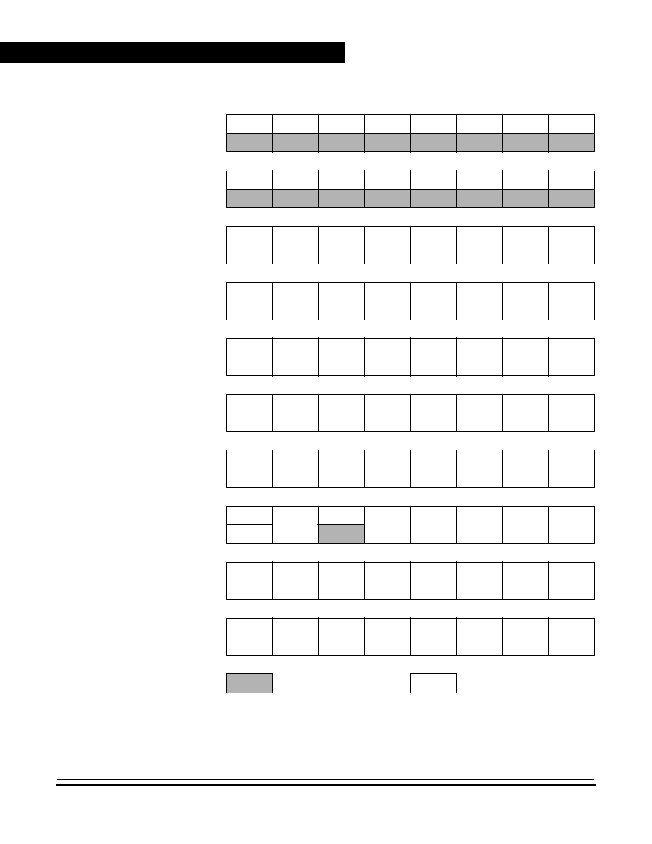
Figure 2-2. Control, Status, and Data Registers (Sheet 1 of 5)

Memory
Monitor ROM
MC68H(R)C08JL3
--
Rev. 4
Technical Data
MOTOROLA
Memory
31
$000B
$000C
Unimplemented
Read:
Write:
$000D
Port A Input Pull-up
Enable Register
(PTAPUE)
Read:
PTA6EN
PTAPUE6 PTAPUE5 PTAPUE4 PTAPUE3 PTAPUE2 PTAPUE1 PTAPUE0
Write:
Reset:
0
0
0
0
0
0
0
0
$000E
$0019
Unimplemented
Read:
Write:
$001A
Keyboard Status and
Control Register
(KBSCR)
Read:
0
0
0
0
KEYF
0
IMASKK
MODEK
Write:
ACKK
Reset:
0
0
0
0
0
0
0
0
$001B
Keyboard Interrupt
Enable Register
(KBIER)
Read:
0
KBIE6
KBIE5
KBIE4
KBIE3
KBIE2
KBIE1
KBIE0
Write:
Reset:
0
0
0
0
0
0
0
0
$001C
Unimplemented
Read:
Write:
$001D
IRQ Status and Control
Register
(INTSCR)
Read:
0
0
0
0
IRQF1
0
IMASK1
MODE1
Write:
ACK1
Reset:
0
0
0
0
0
0
0
0
$001E
Configuration Register 2
(CONFIG2)
Read:
IRQPUD
R
R
LVIT1
LVIT0
R
R
R
Write:
Reset:
0
0
0
0*
0*
0
0
0
$001F
Configuration Register 1
(CONFIG1)
Read:
COPRS
R
R
LVID
R
SSREC
STOP
COPD
Write:
Reset:
0
0
0
0
0
0
0
0
One-time writable register after each reset. * LVIT1 and LVIT0 reset to logic 0 by a power-on reset (POR) only.
$0020
TIM Status and Control
Register
(TSC)
Read:
TOF
TOIE
TSTOP
0
0
PS2
PS1
PS0
Write:
0
TRST
Reset:
0
0
1
0
0
0
0
0
Addr.
Register Name
Bit 7
6
5
4
3
2
1
Bit 0
= Unimplemented
R
= Reserved
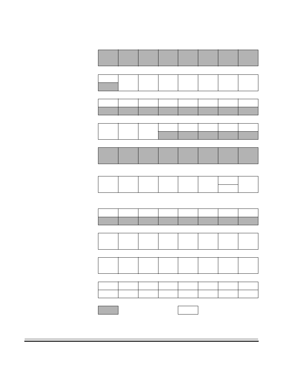
Figure 2-2. Control, Status, and Data Registers (Sheet 2 of 5)
Memory
Technical Data
MC68H(R)C08JL3
--
Rev. 4
32
Memory
MOTOROLA
$0021
TIM Counter Register
High
(TCNTH)
Read:
Bit15
Bit14
Bit13
Bit12
Bit11
Bit10
Bit9
Bit8
Write:
Reset:
0
0
0
0
0
0
0
0
$0022
TIM Counter Register
Low
(TCNTL)
Read:
Bit7
Bit6
Bit5
Bit4
Bit3
Bit2
Bit1
Bit0
Write:
Reset:
0
0
0
0
0
0
0
0
$0023
TIM Counter Modulo
Register High
(TMODH)
Read:
Bit15
Bit14
Bit13
Bit12
Bit11
Bit10
Bit9
Bit8
Write:
Reset:
1
1
1
1
1
1
1
1
$0024
TIM Counter Modulo
Register Low
(TMODL)
Read:
Bit7
Bit6
Bit5
Bit4
Bit3
Bit2
Bit1
Bit0
Write:
Reset:
1
1
1
1
1
1
1
1
$0025
TIM Channel 0 Status and
Control Register
(TSC0)
Read:
CH0F
CH0IE
MS0B
MS0A
ELS0B
ELS0A
TOV0
CH0MAX
Write:
0
Reset:
0
0
0
0
0
0
0
0
$0026
TIM Channel 0
Register High
(TCH0H)
Read:
Bit15
Bit14
Bit13
Bit12
Bit11
Bit10
Bit9
Bit8
Write:
Reset:
Indeterminate after reset
$0027
TIM Channel 0
Register Low
(TCH0L)
Read:
Bit7
Bit6
Bit5
Bit4
Bit3
Bit2
Bit1
Bit0
Write:
Reset:
Indeterminate after reset
$0028
TIM Channel 1 Status and
Control Register
(TSC1)
Read:
CH1F
CH1IE
0
MS1A
ELS1B
ELS1A
TOV1
CH1MAX
Write:
0
Reset:
0
0
0
0
0
0
0
0
$0029
TIM Channel 1
Register High
(TCH1H)
Read:
Bit15
Bit14
Bit13
Bit12
Bit11
Bit10
Bit9
Bit8
Write:
Reset:
Indeterminate after reset
$002A
TIM Channel 1
Register Low
(TCH1L)
Read:
Bit7
Bit6
Bit5
Bit4
Bit3
Bit2
Bit1
Bit0
Write:
Reset:
Indeterminate after reset
Addr.
Register Name
Bit 7
6
5
4
3
2
1
Bit 0
= Unimplemented
R
= Reserved
Figure 2-2. Control, Status, and Data Registers (Sheet 3 of 5)
Memory
Monitor ROM
MC68H(R)C08JL3
--
Rev. 4
Technical Data
MOTOROLA
Memory
33
$002B
$003B
Unimplemented
Read:
Write:
$003C
ADC Status and Control
Register
(ADSCR)
Read:
COCO
AIEN
ADCO
CH4
CH3
CH2
CH1
CH0
Write:
Reset:
0
0
0
1
1
1
1
1
$003D
ADC Data Register
(ADR)
Read:
AD7
AD6
AD5
AD4
AD3
AD2
AD1
AD0
Write:
Reset:
Indeterminate after reset
$003E
ADC Input Clock Register
(ADICLK)
Read:
ADIV2
ADIV1
ADIV0
0
0
0
0
0
Write:
Reset:
0
0
0
0
0
0
0
0
$003F
Unimplemented
Read:
Write:
$FE00
Break Status Register
(BSR)
Read:
R
R
R
R
R
R
SBSW
R
Write:
See note
Reset:
0
Note: Writing a logic 0 clears SBSW.
$FE01
Reset Status Register
(RSR)
Read:
POR
PIN
COP
ILOP
ILAD
MODRST
LVI
0
Write:
POR:
1
0
0
0
0
0
0
0
$FE02
Reserved
Read:
R
R
R
R
R
R
R
R
Write:
$FE03
Break Flag Control
Register
(BFCR)
Read:
BCFE
R
R
R
R
R
R
R
Write:
Reset:
0
$FE04
Interrupt Status Register 1
(INT1)
Read:
0
IF5
IF4
IF3
0
IF1
0
0
Write:
R
R
R
R
R
R
R
R
Reset:
0
0
0
0
0
0
0
0
Addr.
Register Name
Bit 7
6
5
4
3
2
1
Bit 0
= Unimplemented
R
= Reserved
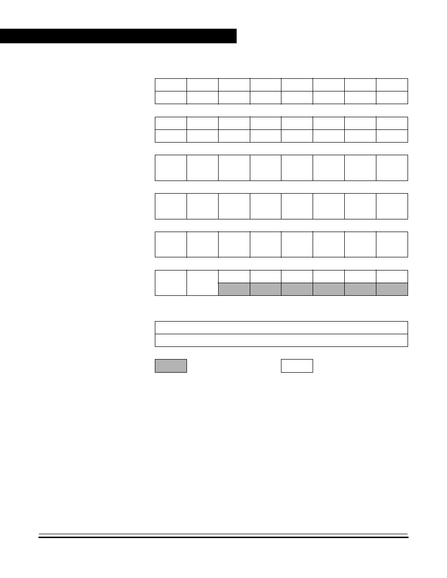
Figure 2-2. Control, Status, and Data Registers (Sheet 4 of 5)
Memory
Technical Data
MC68H(R)C08JL3
--
Rev. 4
34
Memory
MOTOROLA
$FE05
Interrupt Status Register 2
(INT2)
Read:
IF14
0
0
0
0
0
0
0
Write:
R
R
R
R
R
R
R
R
Reset:
0
0
0
0
0
0
0
0
$FE06
Interrupt Status Register 3
(INT3)
Read:
0
0
0
0
0
0
0
IF15
Write:
R
R
R
R
R
R
R
R
Reset:
0
0
0
0
0
0
0
0
$FE07
$FE0B
Reserved
Read:
R
R
R
R
R
R
R
R
Write:
$FE0C
Break Address High
Register
(BRKH)
Read:
Bit15
Bit14
Bit13
Bit12
Bit11
Bit10
Bit9
Bit8
Write:
Reset:
0
0
0
0
0
0
0
0
$FE0D
Break Address low
Register
(BRKL)
Read:
Bit7
Bit6
Bit5
Bit4
Bit3
Bit2
Bit1
Bit0
Write:
Reset:
0
0
0
0
0
0
0
0
$FE0E
Break Status and Control
Register
(BRKSCR)
Read:
BRKE
BRKA
0
0
0
0
0
0
Write:
Reset:
0
0
0
0
0
0
0
0
$FFFF
COP Control Register
(COPCTL)
Read:
Low byte of reset vector
Write:
Writing clears COP counter (any value)
Reset:
Unaffected by reset
Addr.
Register Name
Bit 7
6
5
4
3
2
1
Bit 0
= Unimplemented
R
= Reserved
Figure 2-2. Control, Status, and Data Registers (Sheet 5 of 5)

Memory
Monitor ROM
MC68H(R)C08JL3
--
Rev. 4
Technical Data
MOTOROLA
Memory
35
.
Table 2-1. Vector Addresses
Vector Priority
Vector
Address
Vector
Lowest
IF15
$FFDE
ADC Conversion Complete Vector (High)
$FFDF
ADC Conversion Complete Vector (Low)
IF14
$FFE0
Keyboard Vector (High)
$FFE1
Keyboard Vector (Low)
IF13
to
IF6
--
Not Used
IF5
$FFF2
TIM Overflow Vector (High)
$FFF3
TIM Overflow Vector (Low)
IF4
$FFF4
TIM Channel 1 Vector (High)
$FFF5
TIM Channel 1 Vector (Low)
IF3
$FFF6
TIM Channel 0 Vector (High)
$FFF7
TIM Channel 0 Vector (Low)
IF2
--
Not Used
IF1
$FFFA
IRQ Vector (High)
$FFFB
IRQ Vector (Low)
--
$FFFC
SWI Vector (High)
$FFFD
SWI Vector (Low)
--
$FFFE
Reset Vector (High)
Highest
$FFFF
Reset Vector (Low)

Memory
Technical Data
MC68H(R)C08JL3
--
Rev. 4
36
Memory
MOTOROLA

MC68H(R)C08JL3
--
Rev. 4
Technical Data
MOTOROLA
Random-Access Memory (RAM)
37
Technical Data -- MC68H(R)C08JL3
Section 3. Random-Access Memory (RAM)
3.1 Contents
3.2
Introduction . . . . . . . . . . . . . . . . . . . . . . . . . . . . . . . . . . . . . . . . 37
3.3
Functional Description . . . . . . . . . . . . . . . . . . . . . . . . . . . . . . . 37
3.2 Introduction
This section describes the 128 bytes of RAM.
3.3 Functional Description
Addresses $0080 through $00FF are RAM locations. The location of the
stack RAM is programmable. The 16-bit stack pointer allows the stack to
be anywhere in the 64-Kbyte memory space.
NOTE:
For correct operation, the stack pointer must point only to RAM
locations.
Within page zero are 128 bytes of RAM. Because the location of the
stack RAM is programmable, all page zero RAM locations can be used
for I/O control and user data or code. When the stack pointer is moved
from its reset location at $00FF, direct addressing mode instructions can
access efficiently all page zero RAM locations. Page zero RAM,
therefore, provides ideal locations for frequently accessed global
variables.
Before processing an interrupt, the CPU uses five bytes of the stack to
save the contents of the CPU registers.
NOTE:
For M6805 compatibility, the H register is not stacked.

Random-Access Memory (RAM)
Technical Data
MC68H(R)C08JL3
--
Rev. 4
38
Random-Access Memory (RAM)
MOTOROLA
During a subroutine call, the CPU uses two bytes of the stack to store
the return address. The stack pointer decrements during pushes and
increments during pulls.
NOTE:
Be careful when using nested subroutines. The CPU may overwrite data
in the RAM during a subroutine or during the interrupt stacking
operation.

MC68H(R)C08JL3
--
Rev. 4
Technical Data
MOTOROLA
Read-Only Memory (ROM)
39
Technical Data -- MC68H(R)C08JL3
Section 4. Read-Only Memory (ROM)
4.1 Contents
4.2
Introduction . . . . . . . . . . . . . . . . . . . . . . . . . . . . . . . . . . . . . . . . 39
4.3
Functional Description . . . . . . . . . . . . . . . . . . . . . . . . . . . . . . . 39
4.2 Introduction
This section describes the 4096 or 1536 bytes of read-only memory
(ROM) and 48 bytes of user vectors.
4.3 Functional Description
These addresses are user ROM locations:
$EC00≠$FBFF; user memory, 4096 bytes on MC68H(R)C08JL3/JK3.
$F600≠$FBFF; user memory, 1536 bytes on MC68H(R)C08JK1.
$FFD0≠$FFFF (These locations are reserved for user-defined interrupt
and reset vectors.)
NOTE:
A security feature prevents viewing of the ROM contents.
1
1. No security feature is absolutely secure. However, Motorola's strategy is to make reading or
copying the ROM contents difficult for unauthorized users.

Read-Only Memory (ROM)
Technical Data
MC68H(R)C08JL3
--
Rev. 4
40
Read-Only Memory (ROM)
MOTOROLA

MC68H(R)C08JL3
--
Rev. 4
Technical Data
MOTOROLA
Configuration Register (CONFIG)
41
Technical Data -- MC68H(R)C08JL3
Section 5. Configuration Register (CONFIG)
5.1 Contents
5.2
Introduction . . . . . . . . . . . . . . . . . . . . . . . . . . . . . . . . . . . . . . . . 41
5.3
Functional Description . . . . . . . . . . . . . . . . . . . . . . . . . . . . . . . 42
5.2 Introduction
This section describes the configuration registers (CONFIG1 and
CONFIG2). The configuration registers enables or disables the following
options:
∑
Stop mode recovery time (32
◊
2OSCOUT cycles or
4096
◊
2OSCOUT cycles)
∑
STOP instruction
∑
Computer operating properly module (COP)
∑
COP reset period (COPRS), (2
13
≠2
4
)
◊
2OSCOUT or
(2
18
≠2
4
)
◊
2OSCOUT
∑
Enable LVI circuit
∑
Select LVI trip voltage

Configuration Register (CONFIG)
Technical Data
MC68H(R)C08JL3
--
Rev. 4
42
Configuration Register (CONFIG)
MOTOROLA
5.3 Functional Description
The configuration register is used in the initialization of various options.
The configuration register can be written once after each reset. All of the
configuration register bits are cleared during reset. Since the various
options affect the operation of the MCU it is recommended that this
register be written immediately after reset. The configuration register is
located at $001E and $001F, and may be read at anytime.
NOTE:
The CONFIG registers are one-time writable by the user after each
reset. Upon a reset, the CONFIG registers default to predetermined
settings as shown in
Figure 5-1
and
Figure 5-2
.
IRQPUD -- IRQ1 Pin Pull-up control bit
1 = Internal Pull-up is disconnected
0 = Internal Pull-up is connected between IRQ1 pin and V
DD
LVIT1, LVIT0 -- Low Voltage Inhibit trip voltage selection bits
Detail description of the LVI control signals is given in
Section 16.
Address:
$001E
Bit 7
6
5
4
3
2
1
Bit 0
Read:
IRQPUD
R
R
LVIT1
LVIT0
R
R
R
Write:
Reset:
0
0
0
Not affected
Not affected
0
0
0
POR:
0
0
0
0
0
0
0
0
R
= Reserved
Figure 5-1. Configuration Register 2 (CONFIG2)

Configuration Register (CONFIG)
Functional Description
MC68H(R)C08JL3
--
Rev. 4
Technical Data
MOTOROLA
Configuration Register (CONFIG)
43
COPRS -- COP reset period selection bit
1 = COP reset cycle = (2
13
≠ 2
4
)
◊
2OSCOUT
0 = COP reset cycle = (2
18
≠ 2
4
)
◊
2OSCOUT
LVID -- Low Voltage Inhibit Disable Bit
1 = Low Voltage Inhibit disabled
0 = Low Voltage Inhibit enabled
SSREC -- Short Stop Recovery Bit
SSREC enables the CPU to exit stop mode with a delay of
32
◊
OSCXCLK cycles instead of a 4096
◊
2OSCOUT cycle delay.
1 = Stop mode recovery after 32
◊
2OSCOUT cycles
0 = Stop mode recovery after 4096
◊
2OSCOUT cycles
NOTE:
Exiting stop mode by pulling reset will result in the long stop recovery.
If using an external crystal, do not set the SSREC bit.
STOP enables the STOP instruction.
1 = STOP instruction enabled
0 = STOP instruction treated as illegal opcode
COPD -- COP Disable Bit
COPD disables the COP module. (See
Section 15. Computer
Operating Properly (COP)
.)
1 = COP module disabled
0 = COP module enabled
Address:
$001F
Bit 7
6
5
4
3
2
1
Bit 0
Read:
COPRS
R
R
LVID
R
SSREC
STOP
COPD
Write:
Reset:
0
0
0
0
0
0
0
0
R
= Reserved
Figure 5-2. Configuration Register 1 (CONFIG1)

Configuration Register (CONFIG)
Technical Data
MC68H(R)C08JL3
--
Rev. 4
44
Configuration Register (CONFIG)
MOTOROLA

MC68H(R)C08JL3
--
Rev. 4
Technical Data
MOTOROLA
Central Processor Unit (CPU)
45
Technical Data -- MC68H(R)C08JL3
Section 6. Central Processor Unit (CPU)
6.1 Contents
6.2
Introduction . . . . . . . . . . . . . . . . . . . . . . . . . . . . . . . . . . . . . . . . 45
6.3
Features . . . . . . . . . . . . . . . . . . . . . . . . . . . . . . . . . . . . . . . . . . 46
6.4
CPU Registers . . . . . . . . . . . . . . . . . . . . . . . . . . . . . . . . . . . . . 46
6.4.1
Accumulator . . . . . . . . . . . . . . . . . . . . . . . . . . . . . . . . . . . . . 47
6.4.2
Index Register . . . . . . . . . . . . . . . . . . . . . . . . . . . . . . . . . . . 48
6.4.3
Stack Pointer . . . . . . . . . . . . . . . . . . . . . . . . . . . . . . . . . . . . 48
6.4.4
Program Counter . . . . . . . . . . . . . . . . . . . . . . . . . . . . . . . . . 49
6.4.5
Condition Code Register . . . . . . . . . . . . . . . . . . . . . . . . . . . 49
6.5
Arithmetic/Logic Unit (ALU) . . . . . . . . . . . . . . . . . . . . . . . . . . . 52
6.6
Low-Power Modes . . . . . . . . . . . . . . . . . . . . . . . . . . . . . . . . . . 52
6.6.1
Wait Mode . . . . . . . . . . . . . . . . . . . . . . . . . . . . . . . . . . . . . . 52
6.6.2
Stop Mode . . . . . . . . . . . . . . . . . . . . . . . . . . . . . . . . . . . . . . 53
6.7
CPU During Break Interrupts . . . . . . . . . . . . . . . . . . . . . . . . . . 53
6.8
Instruction Set Summary . . . . . . . . . . . . . . . . . . . . . . . . . . . . 53
6.9
Opcode Map . . . . . . . . . . . . . . . . . . . . . . . . . . . . . . . . . . . . . . . 53
6.2 Introduction
The M68HC08 CPU (central processor unit) is an enhanced and fully
object-code-compatible version of the M68HC05 CPU. The
CPU08
Reference Manual (Motorola document order number CPU08RM/AD)
contains a description of the CPU instruction set, addressing modes,
and architecture.

Central Processor Unit (CPU)
Technical Data
MC68H(R)C08JL3
--
Rev. 4
46
Central Processor Unit (CPU)
MOTOROLA
6.3 Features
∑
Object code fully upward-compatible with M68HC05 Family
∑
16-bit stack pointer with stack manipulation instructions
∑
16-bit index register with x-register manipulation instructions
∑
8-MHz CPU internal bus frequency
∑
64-Kbyte program/data memory space
∑
16 addressing modes
∑
Memory-to-memory data moves without using accumulator
∑
Fast 8-bit by 8-bit multiply and 16-bit by 8-bit divide instructions
∑
Enhanced binary-coded decimal (BCD) data handling
∑
Modular architecture with expandable internal bus definition for
extension of addressing range beyond 64 Kbytes
∑
Low-power stop and wait modes
6.4 CPU Registers
Figure 6-1
shows the five CPU registers. CPU registers are not part of
the memory map.
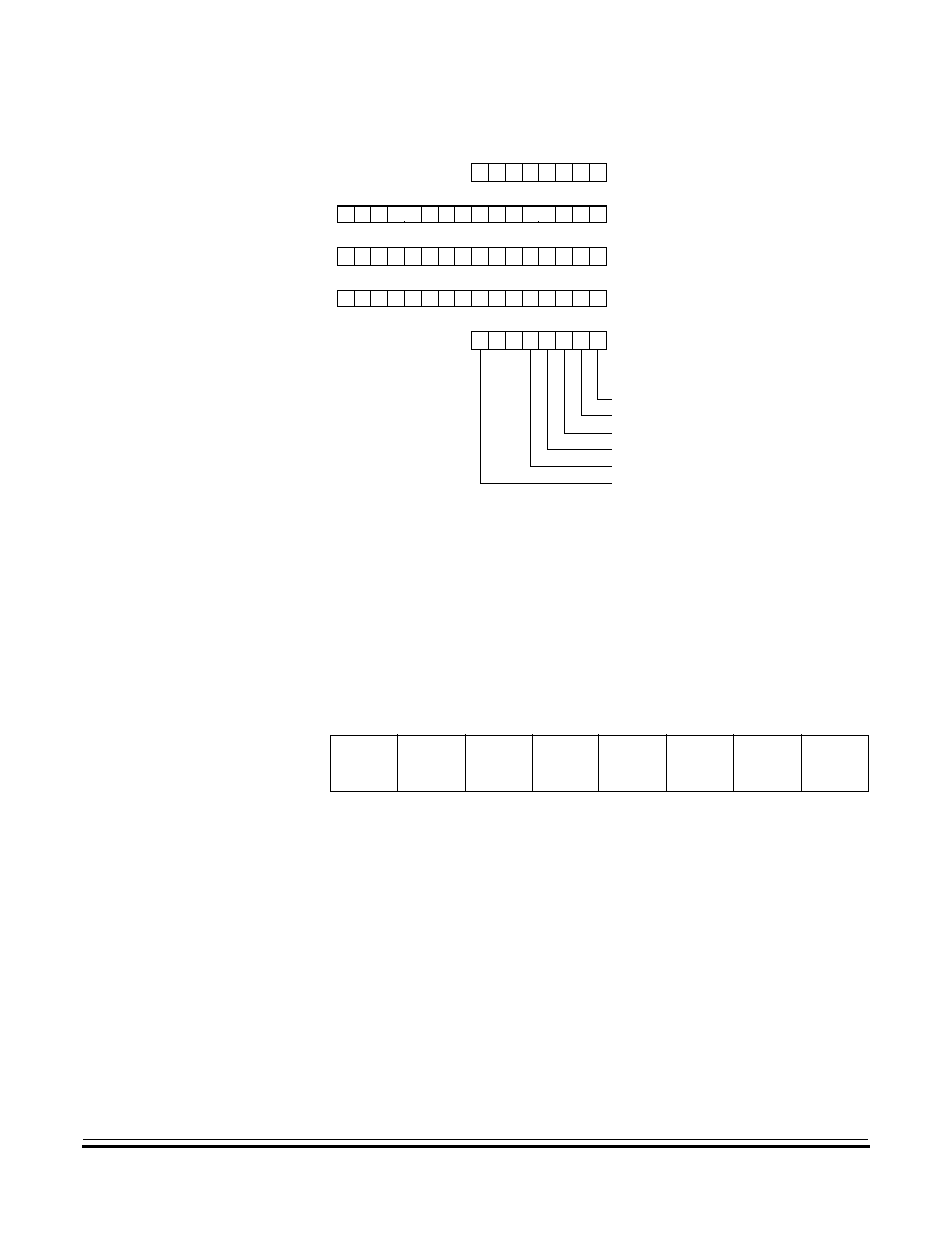
Central Processor Unit (CPU)
CPU Registers
MC68H(R)C08JL3
--
Rev. 4
Technical Data
MOTOROLA
Central Processor Unit (CPU)
47
Figure 6-1. CPU Registers
6.4.1 Accumulator
The accumulator is a general-purpose 8-bit register. The CPU uses the
accumulator to hold operands and the results of arithmetic/logic
operations.
ACCUMULATOR (A)
INDEX REGISTER (H:X)
STACK POINTER (SP)
PROGRAM COUNTER (PC)
CONDITION CODE REGISTER (CCR)
CARRY/BORROW FLAG
ZERO FLAG
NEGATIVE FLAG
INTERRUPT MASK
HALF-CARRY FLAG
TWO'S COMPLEMENT OVERFLOW FLAG
V 1 1 H
I
N Z C
H
X
0
0
0
0
7
15
15
15
7
0
Bit 7
6
5
4
3
2
1
Bit 0
Read:
Write:
Reset:
Unaffected by reset
Figure 6-2. Accumulator (A)

Central Processor Unit (CPU)
Technical Data
MC68H(R)C08JL3
--
Rev. 4
48
Central Processor Unit (CPU)
MOTOROLA
6.4.2 Index Register
The 16-bit index register allows indexed addressing of a 64-Kbyte
memory space. H is the upper byte of the index register, and X is the
lower byte. H:X is the concatenated 16-bit index register.
In the indexed addressing modes, the CPU uses the contents of the
index register to determine the conditional address of the operand.
The index register can serve also as a temporary data storage location.
6.4.3 Stack Pointer
The stack pointer is a 16-bit register that contains the address of the next
location on the stack. During a reset, the stack pointer is preset to
$00FF. The reset stack pointer (RSP) instruction sets the least
significant byte to $FF and does not affect the most significant byte. The
stack pointer decrements as data is pushed onto the stack and
increments as data is pulled from the stack.
In the stack pointer 8-bit offset and 16-bit offset addressing modes, the
stack pointer can function as an index register to access data on the
stack. The CPU uses the contents of the stack pointer to determine the
conditional address of the operand.
Bit
15
14
13
12
11
10
9
8
7
6
5
4
3
2
1
Bit
0
Read:
Write:
Reset:
0
0
0
0
0
0
0
0
X
X
X
X
X
X
X
X
X = Indeterminate
Figure 6-3. Index Register (H:X)

Central Processor Unit (CPU)
CPU Registers
MC68H(R)C08JL3
--
Rev. 4
Technical Data
MOTOROLA
Central Processor Unit (CPU)
49
NOTE:
The location of the stack is arbitrary and may be relocated anywhere in
RAM. Moving the SP out of page 0 ($0000 to $00FF) frees direct
address (page 0) space. For correct operation, the stack pointer must
point only to RAM locations.
6.4.4 Program Counter
The program counter is a 16-bit register that contains the address of the
next instruction or operand to be fetched.
Normally, the program counter automatically increments to the next
sequential memory location every time an instruction or operand is
fetched. Jump, branch, and interrupt operations load the program
counter with an address other than that of the next sequential location.
During reset, the program counter is loaded with the reset vector
address located at $FFFE and $FFFF. The vector address is the
address of the first instruction to be executed after exiting the reset state.
6.4.5 Condition Code Register
The 8-bit condition code register contains the interrupt mask and five
flags that indicate the results of the instruction just executed. Bits 6 and
Bit
15
14
13
12
11
10
9
8
7
6
5
4
3
2
1
Bit
0
Read:
Write:
Reset:
0
0
0
0
0
0
0
0
1
1
1
1
1
1
1
1
Figure 6-4. Stack Pointer (SP)
Bit
15
14
13
12
11
10
9
8
7
6
5
4
3
2
1
Bit
0
Read:
Write:
Reset:
Loaded with Vector from $FFFE and $FFFF
Figure 6-5. Program Counter (PC)

Central Processor Unit (CPU)
Technical Data
MC68H(R)C08JL3
--
Rev. 4
50
Central Processor Unit (CPU)
MOTOROLA
5 are set permanently to logic 1. The following paragraphs describe the
functions of the condition code register.
V -- Overflow Flag
The CPU sets the overflow flag when a two's complement overflow
occurs. The signed branch instructions BGT, BGE, BLE, and BLT use
the overflow flag.
1 = Overflow
0 = No overflow
H -- Half-Carry Flag
The CPU sets the half-carry flag when a carry occurs between
accumulator bits 3 and 4 during an add-without-carry (ADD) or add-
with-carry (ADC) operation. The half-carry flag is required for binary-
coded decimal (BCD) arithmetic operations. The DAA instruction uses
the states of the H and C flags to determine the appropriate correction
factor.
1 = Carry between bits 3 and 4
0 = No carry between bits 3 and 4
Bit 7
6
5
4
3
2
1
Bit 0
Read:
V
1
1
H
I
N
Z
C
Write:
Reset:
X
1
1
X
1
X
X
X
X = Indeterminate
Figure 6-6. Condition Code Register (CCR)

Central Processor Unit (CPU)
CPU Registers
MC68H(R)C08JL3
--
Rev. 4
Technical Data
MOTOROLA
Central Processor Unit (CPU)
51
I -- Interrupt Mask
When the interrupt mask is set, all maskable CPU interrupts are
disabled. CPU interrupts are enabled when the interrupt mask is
cleared. When a CPU interrupt occurs, the interrupt mask is set
automatically after the CPU registers are saved on the stack, but
before the interrupt vector is fetched.
1 = Interrupts disabled
0 = Interrupts enabled
NOTE:
To maintain M6805 Family compatibility, the upper byte of the index
register (H) is not stacked automatically. If the interrupt service routine
modifies H, then the user must stack and unstack H using the PSHH and
PULH instructions.
After the I bit is cleared, the highest-priority interrupt request is
serviced first.
A return-from-interrupt (RTI) instruction pulls the CPU registers from
the stack and restores the interrupt mask from the stack. After any
reset, the interrupt mask is set and can be cleared only by the clear
interrupt mask software instruction (CLI).
N -- Negative flag
The CPU sets the negative flag when an arithmetic operation, logic
operation, or data manipulation produces a negative result, setting bit
7 of the result.
1 = Negative result
0 = Non-negative result
Z -- Zero flag
The CPU sets the zero flag when an arithmetic operation, logic
operation, or data manipulation produces a result of $00.
1 = Zero result
0 = Non-zero result

Central Processor Unit (CPU)
Technical Data
MC68H(R)C08JL3
--
Rev. 4
52
Central Processor Unit (CPU)
MOTOROLA
C -- Carry/Borrow Flag
The CPU sets the carry/borrow flag when an addition operation
produces a carry out of bit 7 of the accumulator or when a subtraction
operation requires a borrow. Some instructions -- such as bit test and
branch, shift, and rotate -- also clear or set the carry/borrow flag.
1 = Carry out of bit 7
0 = No carry out of bit 7
6.5 Arithmetic/Logic Unit (ALU)
The ALU performs the arithmetic and logic operations defined by the
instruction set.
Refer to the
CPU08 Reference Manual (Motorola document order
number CPU08RM/AD) for a description of the instructions and
addressing modes and more detail about the architecture of the CPU.
6.6 Low-Power Modes
The WAIT and STOP instructions put the MCU in low power-consumption
standby modes.
6.6.1 Wait Mode
The WAIT instruction:
∑
Clears the interrupt mask (I bit) in the condition code register,
enabling interrupts. After exit from wait mode by interrupt, the I bit
remains clear. After exit by reset, the I bit is set.
∑
Disables the CPU clock

Central Processor Unit (CPU)
CPU During Break Interrupts
MC68H(R)C08JL3
--
Rev. 4
Technical Data
MOTOROLA
Central Processor Unit (CPU)
53
6.6.2 Stop Mode
The STOP instruction:
∑
Clears the interrupt mask (I bit) in the condition code register,
enabling external interrupts. After exit from stop mode by external
interrupt, the I bit remains clear. After exit by reset, the I bit is set.
∑
Disables the CPU clock
After exiting stop mode, the CPU clock begins running after the oscillator
stabilization delay.
6.7 CPU During Break Interrupts
If a break module is present on the MCU, the CPU starts a break
interrupt by:
∑
Loading the instruction register with the SWI instruction
∑
Loading the program counter with $FFFC:$FFFD or with
$FEFC:$FEFD in monitor mode
The break interrupt begins after completion of the CPU instruction in
progress. If the break address register match occurs on the last cycle of
a CPU instruction, the break interrupt begins immediately.
A return-from-interrupt instruction (RTI) in the break routine ends the
break interrupt and returns the MCU to normal operation if the break
interrupt has been deasserted.
6.8 Instruction Set Summary
6.9 Opcode Map
See
Table 6-2
.
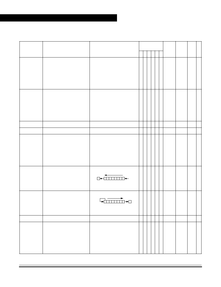
Central Processor Unit (CPU)
Technical Data
MC68H(R)C08JL3
--
Rev. 4
54
Central Processor Unit (CPU)
MOTOROLA
Table 6-1. Instruction Set Summary
Source
Form
Operation
Description
Effect on
CCR
Address
Mode
Opcode
Operand
Cycles
V H I N Z C
ADC #
opr
ADC
opr
ADC
opr
ADC
opr,X
ADC
opr,X
ADC ,X
ADC
opr,SP
ADC
opr,SP
Add with Carry
A
(A) + (M) + (C)
§ §
≠
§ § §
IMM
DIR
EXT
IX2
IX1
IX
SP1
SP2
A9
B9
C9
D9
E9
F9
9EE9
9ED9
ii
dd
hh ll
ee ff
ff
ff
ee ff
2
3
4
4
3
2
4
5
ADD #
opr
ADD
opr
ADD
opr
ADD
opr,X
ADD
opr,X
ADD ,X
ADD
opr,SP
ADD
opr,SP
Add without Carry
A
(A) + (M)
§ §
≠
§ § §
IMM
DIR
EXT
IX2
IX1
IX
SP1
SP2
AB
BB
CB
DB
EB
FB
9EEB
9EDB
ii
dd
hh ll
ee ff
ff
ff
ee ff
2
3
4
4
3
2
4
5
AIS #
opr
Add Immediate Value (Signed) to SP
SP
(SP) + (16 ´ M)
≠ ≠ ≠ ≠ ≠ ≠ IMM
A7
ii 2
AIX #
opr
Add Immediate Value (Signed) to H:X
H:X
(H:X) + (16 ´ M)
≠ ≠ ≠ ≠ ≠ ≠ IMM
AF
ii
2
AND #
opr
AND
opr
AND
opr
AND
opr,X
AND
opr,X
AND ,X
AND
opr,SP
AND
opr,SP
Logical AND
A
(A) & (M)
0 ≠ ≠
§ §
≠
IMM
DIR
EXT
IX2
IX1
IX
SP1
SP2
A4
B4
C4
D4
E4
F4
9EE4
9ED4
ii
dd
hh ll
ee ff
ff
ff
ee ff
2
3
4
4
3
2
4
5
ASL
opr
ASLA
ASLX
ASL
opr,X
ASL ,X
ASL
opr,SP
Arithmetic Shift Left
(Same as LSL)
§
≠ ≠
§ § §
DIR
INH
INH
IX1
IX
SP1
38
48
58
68
78
9E68
dd
ff
ff
4
1
1
4
3
5
ASR
opr
ASRA
ASRX
ASR
opr,X
ASR
opr,X
ASR
opr,SP
Arithmetic Shift Right
§
≠ ≠
§ § §
DIR
INH
INH
IX1
IX
SP1
37
47
57
67
77
9E67
dd
ff
ff
4
1
1
4
3
5
BCC
rel
Branch if Carry Bit Clear
PC
(PC) + 2 + rel ? (C) = 0
≠ ≠ ≠ ≠ ≠ ≠ REL
24
rr
3
BCLR
n, opr
Clear Bit n in M
Mn
0
≠ ≠ ≠ ≠ ≠ ≠
DIR (b0)
DIR (b1)
DIR (b2)
DIR (b3)
DIR (b4)
DIR (b5)
DIR (b6)
DIR (b7)
11
13
15
17
19
1B
1D
1F
dd
dd
dd
dd
dd
dd
dd
dd
4
4
4
4
4
4
4
4
C
b0
b7
0
b0
b7
C
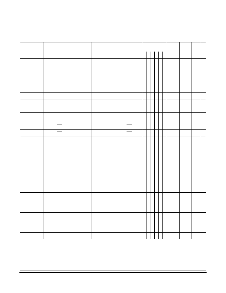
Central Processor Unit (CPU)
Opcode Map
MC68H(R)C08JL3
--
Rev. 4
Technical Data
MOTOROLA
Central Processor Unit (CPU)
55
BCS
rel
Branch if Carry Bit Set (Same as BLO)
PC
(PC) + 2 +
rel ? (C) = 1
≠ ≠ ≠ ≠ ≠ ≠ REL
25
rr
3
BEQ
rel
Branch if Equal
PC
(PC) + 2 +
rel ? (Z) = 1
≠ ≠ ≠ ≠ ≠ ≠ REL
27
rr
3
BGE
opr
Branch if Greater Than or Equal To
(Signed Operands)
PC
(PC) + 2 +
rel ? (N
V
) = 0
≠ ≠ ≠ ≠ ≠ ≠ REL
90
rr
3
BGT
opr
Branch if Greater Than (Signed
Operands)
PC
(PC) + 2 +
rel ? (Z)
| (N
V
) =
0
≠ ≠ ≠ ≠ ≠ ≠ REL
92
rr
3
BHCC
rel
Branch if Half Carry Bit Clear
PC
(PC) + 2 +
rel ? (H) = 0
≠ ≠ ≠ ≠ ≠ ≠ REL
28
rr
3
BHCS
rel
Branch if Half Carry Bit Set
PC
(PC) + 2 +
rel ? (H) = 1
≠ ≠ ≠ ≠ ≠ ≠ REL
29
rr
3
BHI
rel
Branch if Higher
PC
(PC) + 2 +
rel ? (C) | (Z) = 0
≠ ≠ ≠ ≠ ≠ ≠ REL
22
rr
3
BHS
rel
Branch if Higher or Same
(Same as BCC)
PC
(PC) + 2 +
rel ? (C) = 0
≠ ≠ ≠ ≠ ≠ ≠ REL
24
rr
3
BIH
rel
Branch if IRQ Pin High
PC
(PC) + 2 +
rel ? IRQ = 1
≠ ≠ ≠ ≠ ≠ ≠ REL
2F
rr
3
BIL
rel
Branch if IRQ Pin Low
PC
(PC) + 2 +
rel ? IRQ = 0
≠ ≠ ≠ ≠ ≠ ≠ REL
2E
rr
3
BIT #
opr
BIT
opr
BIT
opr
BIT
opr,X
BIT
opr,X
BIT ,X
BIT
opr,SP
BIT
opr,SP
Bit Test
(A) & (M)
0 ≠ ≠
§ §
≠
IMM
DIR
EXT
IX2
IX1
IX
SP1
SP2
A5
B5
C5
D5
E5
F5
9EE5
9ED5
ii
dd
hh ll
ee ff
ff
ff
ee ff
2
3
4
4
3
2
4
5
BLE
opr
Branch if Less Than or Equal To
(Signed Operands)
PC
(PC) + 2 +
rel ? (Z)
| (N
V
) =
1
≠ ≠ ≠ ≠ ≠ ≠ REL
93
rr
3
BLO
rel
Branch if Lower (Same as BCS)
PC
(PC) + 2 +
rel ? (C) = 1
≠ ≠ ≠ ≠ ≠ ≠ REL
25
rr
3
BLS
rel
Branch if Lower or Same
PC
(PC) + 2 +
rel ? (C) | (Z) = 1
≠ ≠ ≠ ≠ ≠ ≠ REL
23
rr
3
BLT
opr
Branch if Less Than (Signed Operands)
PC
(PC) + 2 +
rel ? (N
V
) =
1
≠ ≠ ≠ ≠ ≠ ≠ REL
91
rr
3
BMC
rel
Branch if Interrupt Mask Clear
PC
(PC) + 2 +
rel ? (I) = 0
≠ ≠ ≠ ≠ ≠ ≠ REL
2C
rr
3
BMI
rel
Branch if Minus
PC
(PC) + 2 +
rel ? (N) = 1
≠ ≠ ≠ ≠ ≠ ≠ REL
2B
rr
3
BMS
rel
Branch if Interrupt Mask Set
PC
(PC) + 2 +
rel ? (I) = 1
≠ ≠ ≠ ≠ ≠ ≠ REL
2D
rr
3
BNE
rel
Branch if Not Equal
PC
(PC) + 2 +
rel ? (Z) = 0
≠ ≠ ≠ ≠ ≠ ≠ REL
26
rr
3
BPL
rel
Branch if Plus
PC
(PC) + 2 +
rel ? (N) = 0
≠ ≠ ≠ ≠ ≠ ≠ REL
2A
rr
3
BRA
rel
Branch Always
PC
(PC) + 2 +
rel ≠ ≠ ≠ ≠ ≠ ≠ REL
20
rr
3
Table 6-1. Instruction Set Summary
Source
Form
Operation
Description
Effect on
CCR
Address
Mode
Opcode
Operand
Cycles
V H I N Z C

Central Processor Unit (CPU)
Technical Data
MC68H(R)C08JL3
--
Rev. 4
56
Central Processor Unit (CPU)
MOTOROLA
BRCLR
n,opr,rel Branch if Bit n in M Clear
PC
(PC) + 3 +
rel ? (Mn) = 0
≠ ≠ ≠ ≠ ≠
§
DIR (b0)
DIR (b1)
DIR (b2)
DIR (b3)
DIR (b4)
DIR (b5)
DIR (b6)
DIR (b7)
01
03
05
07
09
0B
0D
0F
dd rr
dd rr
dd rr
dd rr
dd rr
dd rr
dd rr
dd rr
5
5
5
5
5
5
5
5
BRN
rel
Branch Never
PC
(PC) + 2
≠ ≠ ≠ ≠ ≠ ≠ REL
21
rr
3
BRSET
n,opr,rel Branch if Bit n in M Set
PC
(PC) + 3 +
rel ? (Mn) = 1
≠ ≠ ≠ ≠ ≠
§
DIR (b0)
DIR (b1)
DIR (b2)
DIR (b3)
DIR (b4)
DIR (b5)
DIR (b6)
DIR (b7)
00
02
04
06
08
0A
0C
0E
dd rr
dd rr
dd rr
dd rr
dd rr
dd rr
dd rr
dd rr
5
5
5
5
5
5
5
5
BSET
n,opr
Set Bit
n in M
Mn
1
≠ ≠ ≠ ≠ ≠ ≠
DIR (b0)
DIR (b1)
DIR (b2)
DIR (b3)
DIR (b4)
DIR (b5)
DIR (b6)
DIR (b7)
10
12
14
16
18
1A
1C
1E
dd
dd
dd
dd
dd
dd
dd
dd
4
4
4
4
4
4
4
4
BSR
rel
Branch to Subroutine
PC
(PC) + 2; push (PCL)
SP
(SP) ≠ 1; push (PCH)
SP
(SP) ≠ 1
PC
(PC) +
rel
≠ ≠ ≠ ≠ ≠ ≠ REL
AD
rr
4
CBEQ
opr,rel
CBEQA #
opr,rel
CBEQX #
opr,rel
CBEQ
opr,X+,rel
CBEQ
X+,rel
CBEQ
opr,SP,rel
Compare and Branch if Equal
PC
(PC) + 3 + rel ? (A) ≠ (M) = $00
PC
(PC) + 3 + rel ? (A) ≠ (M) = $00
PC
(PC) + 3 + rel ? (X) ≠ (M) = $00
PC
(PC) + 3 + rel ? (A) ≠ (M) = $00
PC
(PC) + 2 + rel ? (A) ≠ (M) = $00
PC
(PC) + 4 + rel ? (A) ≠ (M) = $00
≠ ≠ ≠ ≠ ≠ ≠
DIR
IMM
IMM
IX1+
IX+
SP1
31
41
51
61
71
9E61
dd rr
ii rr
ii rr
ff rr
rr
ff rr
5
4
4
5
4
6
CLC
Clear Carry Bit
C
0
≠ ≠ ≠ ≠ ≠ 0 INH
98
1
CLI
Clear Interrupt Mask
I
0
≠ ≠ 0 ≠ ≠ ≠ INH
9A
2
CLR
opr
CLRA
CLRX
CLRH
CLR
opr,X
CLR ,X
CLR
opr,SP
Clear
M
$00
A
$00
X
$00
H
$00
M
$00
M
$00
M
$00
0 ≠ ≠ 0 1 ≠
DIR
INH
INH
INH
IX1
IX
SP1
3F
4F
5F
8C
6F
7F
9E6F
dd
ff
ff
3
1
1
1
3
2
4
Table 6-1. Instruction Set Summary
Source
Form
Operation
Description
Effect on
CCR
Address
Mode
Opcode
Operand
Cycles
V H I N Z C
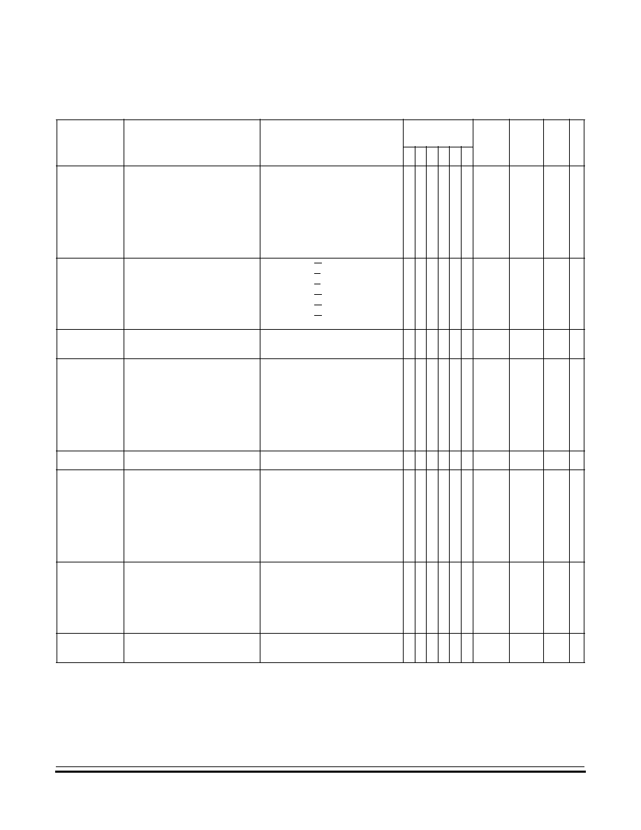
Central Processor Unit (CPU)
Opcode Map
MC68H(R)C08JL3
--
Rev. 4
Technical Data
MOTOROLA
Central Processor Unit (CPU)
57
CMP #
opr
CMP
opr
CMP
opr
CMP
opr,X
CMP
opr,X
CMP ,X
CMP
opr,SP
CMP
opr,SP
Compare A with M
(A) ≠ (M)
§
≠ ≠
§ § §
IMM
DIR
EXT
IX2
IX1
IX
SP1
SP2
A1
B1
C1
D1
E1
F1
9EE1
9ED1
ii
dd
hh ll
ee ff
ff
ff
ee ff
2
3
4
4
3
2
4
5
COM
opr
COMA
COMX
COM
opr,X
COM ,X
COM
opr,SP
Complement (One's Complement)
M
(M) = $FF ≠ (M)
A
(A) = $FF ≠ (M)
X
(X) = $FF ≠ (M)
M
(M) = $FF ≠ (M)
M
(M) = $FF ≠ (M)
M
(M) = $FF ≠ (M)
0 ≠ ≠
§ §
1
DIR
INH
INH
IX1
IX
SP1
33
43
53
63
73
9E63
dd
ff
ff
4
1
1
4
3
5
CPHX #
opr
CPHX
opr
Compare H:X with M
(H:X) ≠ (M:M + 1)
§
≠ ≠
§ § §
IMM
DIR
65
75
ii ii+1
dd
3
4
CPX #
opr
CPX
opr
CPX
opr
CPX ,X
CPX
opr,X
CPX
opr,X
CPX
opr,SP
CPX
opr,SP
Compare X with M
(X) ≠ (M)
§
≠ ≠
§ § §
IMM
DIR
EXT
IX2
IX1
IX
SP1
SP2
A3
B3
C3
D3
E3
F3
9EE3
9ED3
ii
dd
hh ll
ee ff
ff
ff
ee ff
2
3
4
4
3
2
4
5
DAA
Decimal Adjust A
(A)
10
U ≠ ≠
§ § §
INH
72
2
DBNZ
opr,rel
DBNZA
rel
DBNZX
rel
DBNZ
opr,X,rel
DBNZ X
,rel
DBNZ
opr,SP,rel
Decrement and Branch if Not Zero
A
(A) ≠ 1 or M
(M) ≠ 1 or X
(X) ≠
1
PC
(PC) + 3 +
rel ? (result)
0
PC
(PC) + 2 +
rel ? (result)
0
PC
(PC) + 2 +
rel ? (result)
0
PC
(PC) + 3 +
rel ? (result)
0
PC
(PC) + 2 +
rel ? (result)
0
PC
(PC) + 4 +
rel ? (result)
0
≠ ≠ ≠ ≠ ≠ ≠
DIR
INH
INH
IX1
IX
SP1
3B
4B
5B
6B
7B
9E6B
dd rr
rr
rr
ff rr
rr
ff rr
5
3
3
5
4
6
DEC
opr
DECA
DECX
DEC
opr,X
DEC ,X
DEC
opr,SP
Decrement
M
(M) ≠ 1
A
(A) ≠ 1
X
(X) ≠ 1
M
(M) ≠ 1
M
(M) ≠ 1
M
(M) ≠ 1
§
≠ ≠
§ §
≠
DIR
INH
INH
IX1
IX
SP1
3A
4A
5A
6A
7A
9E6A
dd
ff
ff
4
1
1
4
3
5
DIV
Divide
A
(H:A)/(X)
H
Remainder
≠ ≠ ≠ ≠
§ §
INH
52
7
Table 6-1. Instruction Set Summary
Source
Form
Operation
Description
Effect on
CCR
Address
Mode
Opcode
Operand
Cycles
V H I N Z C

Central Processor Unit (CPU)
Technical Data
MC68H(R)C08JL3
--
Rev. 4
58
Central Processor Unit (CPU)
MOTOROLA
EOR #
opr
EOR
opr
EOR
opr
EOR
opr,X
EOR
opr,X
EOR ,X
EOR
opr,SP
EOR
opr,SP
Exclusive OR M with A
A
(A
M)
0 ≠ ≠
§ §
≠
IMM
DIR
EXT
IX2
IX1
IX
SP1
SP2
A8
B8
C8
D8
E8
F8
9EE8
9ED8
ii
dd
hh ll
ee ff
ff
ff
ee ff
2
3
4
4
3
2
4
5
INC
opr
INCA
INCX
INC
opr,X
INC ,X
INC
opr,SP
Increment
M
(M) + 1
A
(A) + 1
X
(X) + 1
M
(M) + 1
M
(M) + 1
M
(M) + 1
§
≠ ≠
§ §
≠
DIR
INH
INH
IX1
IX
SP1
3C
4C
5C
6C
7C
9E6C
dd
ff
ff
4
1
1
4
3
5
JMP
opr
JMP
opr
JMP
opr,X
JMP
opr,X
JMP ,X
Jump
PC
Jump Address
≠ ≠ ≠ ≠ ≠ ≠
DIR
EXT
IX2
IX1
IX
BC
CC
DC
EC
FC
dd
hh ll
ee ff
ff
2
3
4
3
2
JSR
opr
JSR
opr
JSR
opr,X
JSR
opr,X
JSR ,X
Jump to Subroutine
PC
(PC) +
n (n = 1, 2, or 3)
Push (PCL); SP
(SP) ≠ 1
Push (PCH); SP
(SP) ≠ 1
PC
Unconditional Address
≠ ≠ ≠ ≠ ≠ ≠
DIR
EXT
IX2
IX1
IX
BD
CD
DD
ED
FD
dd
hh ll
ee ff
ff
4
5
6
5
4
LDA #
opr
LDA
opr
LDA
opr
LDA
opr,X
LDA
opr,X
LDA ,X
LDA
opr,SP
LDA
opr,SP
Load A from M
A
(M)
0 ≠ ≠
§ §
≠
IMM
DIR
EXT
IX2
IX1
IX
SP1
SP2
A6
B6
C6
D6
E6
F6
9EE6
9ED6
ii
dd
hh ll
ee ff
ff
ff
ee ff
2
3
4
4
3
2
4
5
LDHX #
opr
LDHX
opr
Load H:X from M
H:X
(
M:M
+ 1
)
0 ≠ ≠
§ §
≠
IMM
DIR
45
55
ii jj
dd
3
4
LDX #
opr
LDX
opr
LDX
opr
LDX
opr,X
LDX
opr,X
LDX ,X
LDX
opr,SP
LDX
opr,SP
Load X from M
X
(M)
0 ≠ ≠
§ §
≠
IMM
DIR
EXT
IX2
IX1
IX
SP1
SP2
AE
BE
CE
DE
EE
FE
9EEE
9EDE
ii
dd
hh ll
ee ff
ff
ff
ee ff
2
3
4
4
3
2
4
5
LSL
opr
LSLA
LSLX
LSL
opr,X
LSL ,X
LSL
opr,SP
Logical Shift Left
(Same as ASL)
§
≠ ≠
§ § §
DIR
INH
INH
IX1
IX
SP1
38
48
58
68
78
9E68
dd
ff
ff
4
1
1
4
3
5
Table 6-1. Instruction Set Summary
Source
Form
Operation
Description
Effect on
CCR
Address
Mode
Opcode
Operand
Cycles
V H I N Z C
C
b0
b7
0

Central Processor Unit (CPU)
Opcode Map
MC68H(R)C08JL3
--
Rev. 4
Technical Data
MOTOROLA
Central Processor Unit (CPU)
59
LSR
opr
LSRA
LSR
X
LSR
opr,X
LSR ,X
LSR
opr,SP
Logical Shift Right
§
≠ ≠ 0
§ §
DIR
INH
INH
IX1
IX
SP1
34
44
54
64
74
9E64
dd
ff
ff
4
1
1
4
3
5
MOV
opr,opr
MOV
opr,X+
MOV #
opr,opr
MOV X+
,opr
Move
(M)
Destination
(M)
Source
H:X
(H:X) + 1 (IX+D, DIX+)
0 ≠ ≠
§ §
≠
DD
DIX+
IMD
IX+D
4E
5E
6E
7E
dd dd
dd
ii dd
dd
5
4
4
4
MUL
Unsigned multiply
X:A
(X)
◊
(A)
≠ 0 ≠ ≠ ≠ 0 INH
42
5
NEG
opr
NEGA
NEGX
NEG
opr,X
NEG ,X
NEG
opr,SP
Negate (Two's Complement)
M
≠(M) = $00 ≠ (M)
A
≠(A) = $00 ≠ (A)
X
≠(X) = $00 ≠ (X)
M
≠(M) = $00 ≠ (M)
M
≠(M) = $00 ≠ (M)
§
≠ ≠
§ § §
DIR
INH
INH
IX1
IX
SP1
30
40
50
60
70
9E60
dd
ff
ff
4
1
1
4
3
5
NOP
No Operation
None
≠ ≠ ≠ ≠ ≠ ≠ INH
9D
1
NSA
Nibble Swap A
A
(A[3:0]:A[7:4])
≠ ≠ ≠ ≠ ≠ ≠ INH
62
3
ORA #
opr
ORA
opr
ORA
opr
ORA
opr,X
ORA
opr,X
ORA ,X
ORA
opr,SP
ORA
opr,SP
Inclusive OR A and M
A
(A) | (M)
0 ≠ ≠
§ §
≠
IMM
DIR
EXT
IX2
IX1
IX
SP1
SP2
AA
BA
CA
DA
EA
FA
9EEA
9EDA
ii
dd
hh ll
ee ff
ff
ff
ee ff
2
3
4
4
3
2
4
5
PSHA
Push A onto Stack
Push (A); SP
(SP) ≠ 1
≠ ≠ ≠ ≠ ≠ ≠ INH
87
2
PSHH
Push H onto Stack
Push (H); SP
(SP) ≠ 1
≠ ≠ ≠ ≠ ≠ ≠ INH
8B
2
PSHX
Push X onto Stack
Push (X); SP
(SP) ≠ 1
≠ ≠ ≠ ≠ ≠ ≠ INH
89
2
PULA
Pull A from Stack
SP
(SP + 1); Pull
(
A
)
≠ ≠ ≠ ≠ ≠ ≠ INH
86
2
PULH
Pull H from Stack
SP
(SP + 1); Pull
(
H
)
≠ ≠ ≠ ≠ ≠ ≠ INH
8A
2
PULX
Pull X from Stack
SP
(SP + 1); Pull
(
X
)
≠ ≠ ≠ ≠ ≠ ≠ INH
88
2
ROL
opr
ROLA
ROLX
ROL
opr,X
ROL ,X
ROL
opr,SP
Rotate Left through Carry
§
≠ ≠
§ § §
DIR
INH
INH
IX1
IX
SP1
39
49
59
69
79
9E69
dd
ff
ff
4
1
1
4
3
5
Table 6-1. Instruction Set Summary
Source
Form
Operation
Description
Effect on
CCR
Address
Mode
Opcode
Operand
Cycles
V H I N Z C
b0
b7
C
0
C
b0
b7
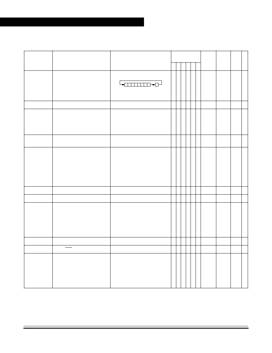
Central Processor Unit (CPU)
Technical Data
MC68H(R)C08JL3
--
Rev. 4
60
Central Processor Unit (CPU)
MOTOROLA
ROR
opr
RORA
RORX
ROR
opr,X
ROR ,X
ROR
opr,SP
Rotate Right through Carry
§
≠ ≠
§ § §
DIR
INH
INH
IX1
IX
SP1
36
46
56
66
76
9E66
dd
ff
ff
4
1
1
4
3
5
RSP
Reset Stack Pointer
SP
$FF
≠ ≠ ≠ ≠ ≠ ≠ INH
9C
1
RTI
Return from Interrupt
SP
(SP) + 1; Pull (CCR)
SP
(SP) + 1; Pull (A)
SP
(SP) + 1; Pull (X)
SP
(SP) + 1; Pull (PCH)
SP
(SP) + 1; Pull (PCL)
§ § § § § §
INH
80
7
RTS
Return from Subroutine
SP
SP + 1
;
Pull
(
PCH)
SP
SP + 1; Pull (PCL)
≠ ≠ ≠ ≠ ≠ ≠ INH
81
4
SBC #
opr
SBC
opr
SBC
opr
SBC
opr,X
SBC
opr,X
SBC ,X
SBC
opr,SP
SBC
opr,SP
Subtract with Carry
A
(A) ≠ (M) ≠ (C)
§
≠ ≠
§ § §
IMM
DIR
EXT
IX2
IX1
IX
SP1
SP2
A2
B2
C2
D2
E2
F2
9EE2
9ED2
ii
dd
hh ll
ee ff
ff
ff
ee ff
2
3
4
4
3
2
4
5
SEC
Set Carry Bit
C
1
≠ ≠ ≠ ≠ ≠ 1 INH
99
1
SEI
Set Interrupt Mask
I
1
≠ ≠ 1 ≠ ≠ ≠ INH
9B
2
STA
opr
STA
opr
STA
opr,X
STA
opr,X
STA ,X
STA
opr,SP
STA
opr,SP
Store A in M
M
(A)
0 ≠ ≠
§ §
≠
DIR
EXT
IX2
IX1
IX
SP1
SP2
B7
C7
D7
E7
F7
9EE7
9ED7
dd
hh ll
ee ff
ff
ff
ee ff
3
4
4
3
2
4
5
STHX
opr
Store H:X in M
(M:M + 1)
(H:X)
0 ≠ ≠
§ §
≠ DIR
35
dd
4
STOP
Enable IRQ Pin; Stop Oscillator
I
0; Stop Oscillator
≠ ≠ 0 ≠ ≠ ≠ INH
8E
1
STX
opr
STX
opr
STX
opr,X
STX
opr,X
STX ,X
STX
opr,SP
STX
opr,SP
Store X in M
M
(X)
0 ≠ ≠
§ §
≠
DIR
EXT
IX2
IX1
IX
SP1
SP2
BF
CF
DF
EF
FF
9EEF
9EDF
dd
hh ll
ee ff
ff
ff
ee ff
3
4
4
3
2
4
5
Table 6-1. Instruction Set Summary
Source
Form
Operation
Description
Effect on
CCR
Address
Mode
Opcode
Operand
Cycles
V H I N Z C
b0
b7
C
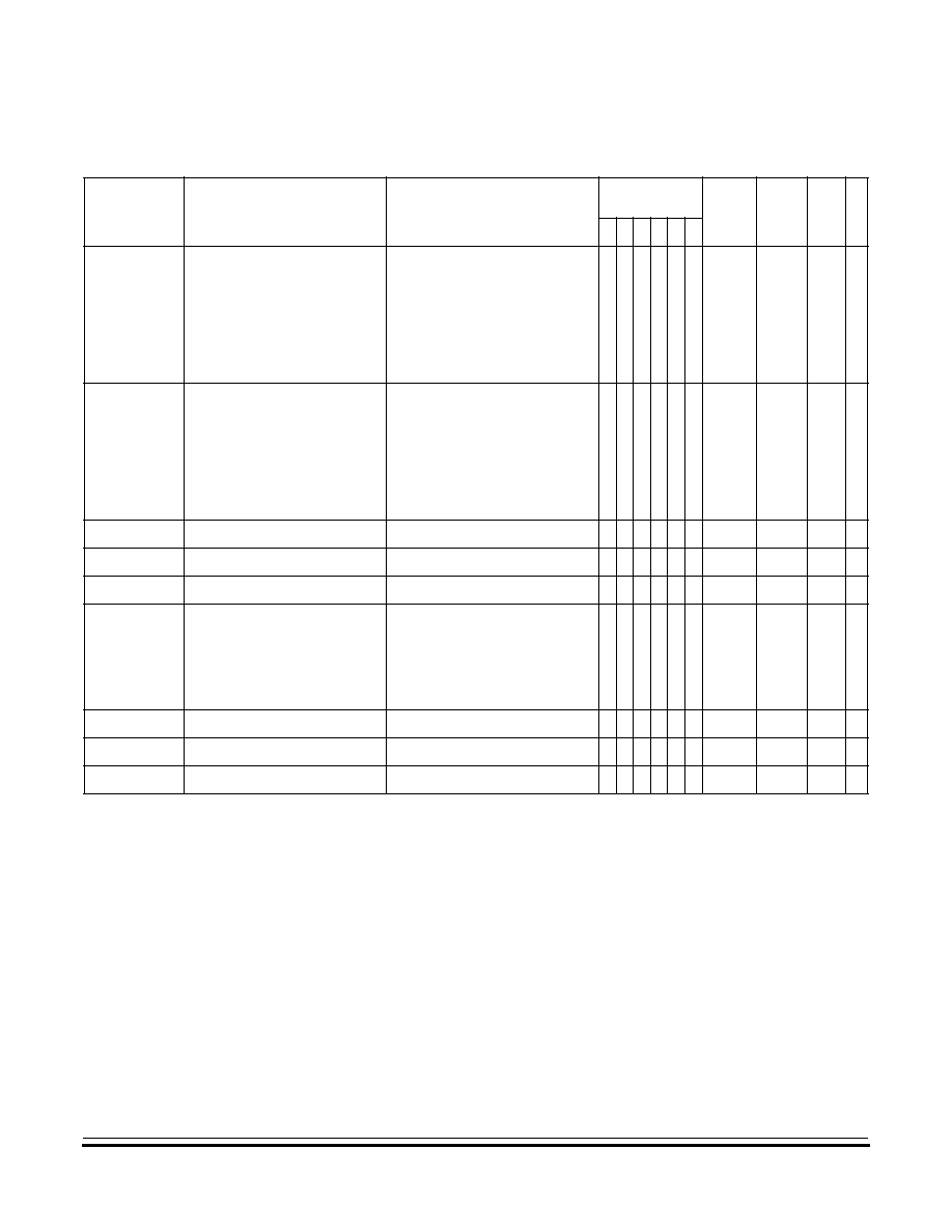
Central Processor Unit (CPU)
Opcode Map
MC68H(R)C08JL3
--
Rev. 4
Technical Data
MOTOROLA
Central Processor Unit (CPU)
61
SUB #
opr
SUB
opr
SUB
opr
SUB
opr,X
SUB
opr,X
SUB ,X
SUB
opr,SP
SUB
opr,SP
Subtract A
(A) ≠ (M)
§
≠ ≠
§ § §
IMM
DIR
EXT
IX2
IX1
IX
SP1
SP2
A0
B0
C0
D0
E0
F0
9EE0
9ED0
ii
dd
hh ll
ee ff
ff
ff
ee ff
2
3
4
4
3
2
4
5
SWI
Software Interrupt
PC
(PC) + 1; Push (PCL)
SP
(SP) ≠ 1; Push (PCH)
SP
(SP) ≠ 1; Push (X)
SP
(SP) ≠ 1; Push (A)
SP
(SP) ≠ 1; Push (CCR)
SP
(SP) ≠ 1; I
1
PCH
Interrupt Vector High Byte
PCL
Interrupt Vector Low Byte
≠ ≠ 1 ≠ ≠ ≠ INH
83
9
TAP
Transfer A to CCR
CCR
(A)
§ § § § § §
INH
84
2
TAX
Transfer A to X
X
(A)
≠ ≠ ≠ ≠ ≠ ≠ INH
97
1
TPA
Transfer CCR to A
A
(CCR)
≠ ≠ ≠ ≠ ≠ ≠ INH
85
1
TST
opr
TSTA
TSTX
TST
opr,X
TST ,X
TST
opr,SP
Test for Negative or Zero
(A) ≠ $00 or (X) ≠ $00 or (M) ≠ $00
0 ≠ ≠
§ §
≠
DIR
INH
INH
IX1
IX
SP1
3D
4D
5D
6D
7D
9E6D
dd
ff
ff
3
1
1
3
2
4
TSX
Transfer SP to H:X
H:X
(SP) + 1
≠ ≠ ≠ ≠ ≠ ≠ INH
95
2
TXA
Transfer X to A
A
(X)
≠ ≠ ≠ ≠ ≠ ≠ INH
9F
1
TXS
Transfer H:X to SP
(SP)
(H:X) ≠ 1
≠ ≠ ≠ ≠ ≠ ≠ INH
94
2
Table 6-1. Instruction Set Summary
Source
Form
Operation
Description
Effect on
CCR
Address
Mode
Opcode
Operand
Cycles
V H I N Z C

Central Processor Unit (CPU)
Technical Data
MC68H(R)C08JL3
--
Rev. 4
62
Central Processor Unit (CPU)
MOTOROLA
A
Accumulator
n
Any bit
C
Carry/borrow bit
opr
Operand (one or two bytes)
CCR
Condition code register
PC
Program counter
dd
Direct address of operand
PCH Program counter high byte
dd rr
Direct address of operand and relative offset of branch instruction
PCL Program counter low byte
DD
Direct to direct addressing mode
REL Relative addressing mode
DIR
Direct addressing mode
rel
Relative program counter offset byte
DIX+
Direct to indexed with post increment addressing mode
rr
Relative program counter offset byte
ee ff
High and low bytes of offset in indexed, 16-bit offset addressing
SP1 Stack pointer, 8-bit offset addressing mode
EXT
Extended addressing mode
SP2 Stack pointer 16-bit offset addressing mode
ff
Offset byte in indexed, 8-bit offset addressing
SP
Stack pointer
H
Half-carry bit
U
Undefined
H
Index register high byte
V
Overflow bit
hh ll
High and low bytes of operand address in extended addressing
X
Index register low byte
I
Interrupt mask
Z
Zero bit
ii
Immediate operand byte
&
Logical AND
IMD
Immediate source to direct destination addressing mode
|
Logical OR
IMM
Immediate addressing mode
Logical EXCLUSIVE OR
INH
Inherent addressing mode
( )
Contents of
IX
Indexed, no offset addressing mode
≠( )
Negation (two's complement)
IX+
Indexed, no offset, post increment addressing mode
#
Immediate value
IX+D
Indexed with post increment to direct addressing mode
´
Sign extend
IX1
Indexed, 8-bit offset addressing mode
Loaded with
IX1+
Indexed, 8-bit offset, post increment addressing mode
?
If
IX2
Indexed, 16-bit offset addressing mode
:
Concatenated with
M
Memory location
§
Set or cleared
N
Negative bit
--
Not affected
Table 6-1. Instruction Set Summary
Source
Form
Operation
Description
Effect on
CCR
Address
Mode
Opcode
Operand
Cycles
V H I N Z C

MC68H(R)C08JL3
--
Re
v
.
4
T
echnical Data
MOTOROLA
Central Processor Unit (CPU)
63
Central Processor Unit (CPU)
Opcode Map
Table 6-2. Opcode Map
Bit Manipulation
Branch
Read-Modify-Write
Control
Register/Memory
DIR
DIR
REL
DIR
INH
INH
IX1
SP1
IX
INH
INH
IMM
DIR
EXT
IX2
SP2
IX1
SP1
IX
0
1
2
3
4
5
6
9E6
7
8
9
A
B
C
D
9ED
E
9EE
F
0
5
BRSET0
3
DIR
4
BSET0
2
DIR
3
BRA
2
REL
4
NEG
2
DIR
1
NEGA
1
INH
1
NEGX
1
INH
4
NEG
2
IX1
5
NEG
3
SP1
3
NEG
1
IX
7
RTI
1
INH
3
BGE
2
REL
2
SUB
2
IMM
3
SUB
2
DIR
4
SUB
3
EXT
4
SUB
3
IX2
5
SUB
4
SP2
3
SUB
2
IX1
4
SUB
3
SP1
2
SUB
1
IX
1
5
BRCLR0
3
DIR
4
BCLR0
2
DIR
3
BRN
2
REL
5
CBEQ
3
DIR
4
CBEQA
3
IMM
4
CBEQX
3
IMM
5
CBEQ
3 IX1+
6
CBEQ
4
SP1
4
CBEQ
2
IX+
4
RTS
1
INH
3
BLT
2
REL
2
CMP
2
IMM
3
CMP
2
DIR
4
CMP
3
EXT
4
CMP
3
IX2
5
CMP
4
SP2
3
CMP
2
IX1
4
CMP
3
SP1
2
CMP
1
IX
2
5
BRSET1
3
DIR
4
BSET1
2
DIR
3
BHI
2
REL
5
MUL
1
INH
7
DIV
1
INH
3
NSA
1
INH
2
DAA
1
INH
3
BGT
2
REL
2
SBC
2
IMM
3
SBC
2
DIR
4
SBC
3
EXT
4
SBC
3
IX2
5
SBC
4
SP2
3
SBC
2
IX1
4
SBC
3
SP1
2
SBC
1
IX
3
5
BRCLR1
3
DIR
4
BCLR1
2
DIR
3
BLS
2
REL
4
COM
2
DIR
1
COMA
1
INH
1
COMX
1
INH
4
COM
2
IX1
5
COM
3
SP1
3
COM
1
IX
9
SWI
1
INH
3
BLE
2
REL
2
CPX
2
IMM
3
CPX
2
DIR
4
CPX
3
EXT
4
CPX
3
IX2
5
CPX
4
SP2
3
CPX
2
IX1
4
CPX
3
SP1
2
CPX
1
IX
4
5
BRSET2
3
DIR
4
BSET2
2
DIR
3
BCC
2
REL
4
LSR
2
DIR
1
LSRA
1
INH
1
LSRX
1
INH
4
LSR
2
IX1
5
LSR
3
SP1
3
LSR
1
IX
2
TAP
1
INH
2
TXS
1
INH
2
AND
2
IMM
3
AND
2
DIR
4
AND
3
EXT
4
AND
3
IX2
5
AND
4
SP2
3
AND
2
IX1
4
AND
3
SP1
2
AND
1
IX
5
5
BRCLR2
3
DIR
4
BCLR2
2
DIR
3
BCS
2
REL
4
STHX
2
DIR
3
LDHX
3
IMM
4
LDHX
2
DIR
3
CPHX
3
IMM
4
CPHX
2
DIR
1
TPA
1
INH
2
TSX
1
INH
2
BIT
2
IMM
3
BIT
2
DIR
4
BIT
3
EXT
4
BIT
3
IX2
5
BIT
4
SP2
3
BIT
2
IX1
4
BIT
3
SP1
2
BIT
1
IX
6
5
BRSET3
3
DIR
4
BSET3
2
DIR
3
BNE
2
REL
4
ROR
2
DIR
1
RORA
1
INH
1
RORX
1
INH
4
ROR
2
IX1
5
ROR
3
SP1
3
ROR
1
IX
2
PULA
1
INH
2
LDA
2
IMM
3
LDA
2
DIR
4
LDA
3
EXT
4
LDA
3
IX2
5
LDA
4
SP2
3
LDA
2
IX1
4
LDA
3
SP1
2
LDA
1
IX
7
5
BRCLR3
3
DIR
4
BCLR3
2
DIR
3
BEQ
2
REL
4
ASR
2
DIR
1
ASRA
1
INH
1
ASRX
1
INH
4
ASR
2
IX1
5
ASR
3
SP1
3
ASR
1
IX
2
PSHA
1
INH
1
TAX
1
INH
2
AIS
2
IMM
3
STA
2
DIR
4
STA
3
EXT
4
STA
3
IX2
5
STA
4
SP2
3
STA
2
IX1
4
STA
3
SP1
2
STA
1
IX
8
5
BRSET4
3
DIR
4
BSET4
2
DIR
3
BHCC
2
REL
4
LSL
2
DIR
1
LSLA
1
INH
1
LSLX
1
INH
4
LSL
2
IX1
5
LSL
3
SP1
3
LSL
1
IX
2
PULX
1
INH
1
CLC
1
INH
2
EOR
2
IMM
3
EOR
2
DIR
4
EOR
3
EXT
4
EOR
3
IX2
5
EOR
4
SP2
3
EOR
2
IX1
4
EOR
3
SP1
2
EOR
1
IX
9
5
BRCLR4
3
DIR
4
BCLR4
2
DIR
3
BHCS
2
REL
4
ROL
2
DIR
1
ROLA
1
INH
1
ROLX
1
INH
4
ROL
2
IX1
5
ROL
3
SP1
3
ROL
1
IX
2
PSHX
1
INH
1
SEC
1
INH
2
ADC
2
IMM
3
ADC
2
DIR
4
ADC
3
EXT
4
ADC
3
IX2
5
ADC
4
SP2
3
ADC
2
IX1
4
ADC
3
SP1
2
ADC
1
IX
A
5
BRSET5
3
DIR
4
BSET5
2
DIR
3
BPL
2
REL
4
DEC
2
DIR
1
DECA
1
INH
1
DECX
1
INH
4
DEC
2
IX1
5
DEC
3
SP1
3
DEC
1
IX
2
PULH
1
INH
2
CLI
1
INH
2
ORA
2
IMM
3
ORA
2
DIR
4
ORA
3
EXT
4
ORA
3
IX2
5
ORA
4
SP2
3
ORA
2
IX1
4
ORA
3
SP1
2
ORA
1
IX
B
5
BRCLR5
3
DIR
4
BCLR5
2
DIR
3
BMI
2
REL
5
DBNZ
3
DIR
3
DBNZA
2
INH
3
DBNZX
2
INH
5
DBNZ
3
IX1
6
DBNZ
4
SP1
4
DBNZ
2
IX
2
PSHH
1
INH
2
SEI
1
INH
2
ADD
2
IMM
3
ADD
2
DIR
4
ADD
3
EXT
4
ADD
3
IX2
5
ADD
4
SP2
3
ADD
2
IX1
4
ADD
3
SP1
2
ADD
1
IX
C
5
BRSET6
3
DIR
4
BSET6
2
DIR
3
BMC
2
REL
4
INC
2
DIR
1
INCA
1
INH
1
INCX
1
INH
4
INC
2
IX1
5
INC
3
SP1
3
INC
1
IX
1
CLRH
1
INH
1
RSP
1
INH
2
JMP
2
DIR
3
JMP
3
EXT
4
JMP
3
IX2
3
JMP
2
IX1
2
JMP
1
IX
D
5
BRCLR6
3
DIR
4
BCLR6
2
DIR
3
BMS
2
REL
3
TST
2
DIR
1
TSTA
1
INH
1
TSTX
1
INH
3
TST
2
IX1
4
TST
3
SP1
2
TST
1
IX
1
NOP
1
INH
4
BSR
2
REL
4
JSR
2
DIR
5
JSR
3
EXT
6
JSR
3
IX2
5
JSR
2
IX1
4
JSR
1
IX
E
5
BRSET7
3
DIR
4
BSET7
2
DIR
3
BIL
2
REL
5
MOV
3
DD
4
MOV
2 DIX+
4
MOV
3
IMD
4
MOV
2 IX+D
1
STOP
1
INH
*
2
LDX
2
IMM
3
LDX
2
DIR
4
LDX
3
EXT
4
LDX
3
IX2
5
LDX
4
SP2
3
LDX
2
IX1
4
LDX
3
SP1
2
LDX
1
IX
F
5
BRCLR7
3
DIR
4
BCLR7
2
DIR
3
BIH
2
REL
3
CLR
2
DIR
1
CLRA
1
INH
1
CLRX
1
INH
3
CLR
2
IX1
4
CLR
3
SP1
2
CLR
1
IX
1
WAIT
1
INH
1
TXA
1
INH
2
AIX
2
IMM
3
STX
2
DIR
4
STX
3
EXT
4
STX
3
IX2
5
STX
4
SP2
3
STX
2
IX1
4
STX
3
SP1
2
STX
1
IX
INH Inherent
REL Relative
SP1 Stack Pointer, 8-Bit Offset
IMM Immediate
IX
Indexed, No Offset
SP2 Stack Pointer, 16-Bit Offset
DIR Direct
IX1
Indexed, 8-Bit Offset
IX+
Indexed, No Offset with
EXT Extended
IX2
Indexed, 16-Bit Offset
Post Increment
DD
Direct-Direct
IMD Immediate-Direct
IX1+ Indexed, 1-Byte Offset with
IX+D Indexed-Direct
DIX+ Direct-Indexed
Post Increment
*
Pre-byte for stack pointer indexed instructions
0
High Byte of Opcode in Hexadecimal
Low Byte of Opcode in Hexadecimal
0
5
BRSET0
3
DIR
Cycles
Opcode Mnemonic
Number of Bytes / Addressing Mode
MSB
LSB
MSB
LSB

Central Processor Unit (CPU)
Technical Data
MC68H(R)C08JL3
--
Rev. 4
64
Central Processor Unit (CPU)
MOTOROLA

MC68H(R)C08JL3
--
Rev. 4
Technical Data
MOTOROLA
System Integration Module (SIM)
65
Technical Data -- MC68H(R)C08JL3
Section 7. System Integration Module (SIM)
7.1 Contents
7.2
Introduction . . . . . . . . . . . . . . . . . . . . . . . . . . . . . . . . . . . . . . . . 66
7.3
SIM Bus Clock Control and Generation . . . . . . . . . . . . . . . . . . 69
7.3.1
Bus Timing . . . . . . . . . . . . . . . . . . . . . . . . . . . . . . . . . . . . . . 69
7.3.2
Clock Start-Up from POR . . . . . . . . . . . . . . . . . . . . . . . . . . . 69
7.3.3
Clocks in Stop Mode and Wait Mode . . . . . . . . . . . . . . . . . . 69
7.4
Reset and System Initialization. . . . . . . . . . . . . . . . . . . . . . . . . 70
7.4.1
External Pin Reset . . . . . . . . . . . . . . . . . . . . . . . . . . . . . . . . 70
7.4.2
Active Resets from Internal Sources . . . . . . . . . . . . . . . . . . 71
7.4.2.1
Power-On Reset . . . . . . . . . . . . . . . . . . . . . . . . . . . . . . . 72
7.4.2.2
Computer Operating Properly (COP) Reset . . . . . . . . . . 73
7.4.2.3
Illegal Opcode Reset . . . . . . . . . . . . . . . . . . . . . . . . . . . . 73
7.4.2.4
Illegal Address Reset . . . . . . . . . . . . . . . . . . . . . . . . . . . . 73
7.4.2.5
LVI Reset . . . . . . . . . . . . . . . . . . . . . . . . . . . . . . . . . . . . . 74
7.5
SIM Counter . . . . . . . . . . . . . . . . . . . . . . . . . . . . . . . . . . . . . . . 74
7.5.1
SIM Counter During Power-On Reset . . . . . . . . . . . . . . . . . 74
7.5.2
SIM Counter During Stop Mode Recovery . . . . . . . . . . . . . . 74
7.5.3
SIM Counter and Reset States. . . . . . . . . . . . . . . . . . . . . . . 75
7.6
Exception Control . . . . . . . . . . . . . . . . . . . . . . . . . . . . . . . . . . . 75
7.6.1
Interrupts . . . . . . . . . . . . . . . . . . . . . . . . . . . . . . . . . . . . . . . 75
7.6.1.1
Hardware Interrupts . . . . . . . . . . . . . . . . . . . . . . . . . . . . . 77
7.6.1.2
SWI Instruction. . . . . . . . . . . . . . . . . . . . . . . . . . . . . . . . . 79
7.6.2
Interrupt Status Registers. . . . . . . . . . . . . . . . . . . . . . . . . . . 79
7.6.2.1
Interrupt Status Register 1 . . . . . . . . . . . . . . . . . . . . . . . 80
7.6.2.2
Interrupt Status Register 2 . . . . . . . . . . . . . . . . . . . . . . . . 80
7.6.2.3
Interrupt Status Register 3 . . . . . . . . . . . . . . . . . . . . . . . . 81
7.6.3
Reset . . . . . . . . . . . . . . . . . . . . . . . . . . . . . . . . . . . . . . . . . . 81
7.6.4
Break Interrupts . . . . . . . . . . . . . . . . . . . . . . . . . . . . . . . . . . 81
7.6.5
Status Flag Protection in Break Mode . . . . . . . . . . . . . . . . . 81

System Integration Module (SIM)
Technical Data
MC68H(R)C08JL3
--
Rev. 4
66
System Integration Module (SIM)
MOTOROLA
7.7
Low-Power Modes . . . . . . . . . . . . . . . . . . . . . . . . . . . . . . . . . . 82
7.7.1
Wait Mode . . . . . . . . . . . . . . . . . . . . . . . . . . . . . . . . . . . . . . 82
7.7.2
Stop Mode . . . . . . . . . . . . . . . . . . . . . . . . . . . . . . . . . . . . . . 84
7.8
SIM Registers . . . . . . . . . . . . . . . . . . . . . . . . . . . . . . . . . . . . . . 85
7.8.1
Break Status Register (BSR) . . . . . . . . . . . . . . . . . . . . . . . . 85
7.8.2
Reset Status Register (RSR) . . . . . . . . . . . . . . . . . . . . . . . . 86
7.8.3
Break Flag Control Register (BFCR) . . . . . . . . . . . . . . . . . . 88
7.2 Introduction
This section describes the system integration module (SIM), which
supports up to 24 external and/or internal interrupts. Together with the
CPU, the SIM controls all MCU activities. A block diagram of the SIM is
shown in
Figure 7-1
.
Figure 7-2
is a summary of the SIM I/O registers.
The SIM is a system state controller that coordinates CPU and exception
timing. The SIM is responsible for:
∑
Bus clock generation and control for CPU and peripherals
≠
Stop/wait/reset/break entry and recovery
≠
Internal clock control
∑
Master reset control, including power-on reset (POR) and COP
timeout
∑
Interrupt control:
≠
Acknowledge timing
≠
Arbitration control timing
≠
Vector address generation
∑
CPU enable/disable timing
∑
Modular architecture expandable to 128 interrupt sources

System Integration Module (SIM)
Introduction
MC68H(R)C08JL3
--
Rev. 4
Technical Data
MOTOROLA
System Integration Module (SIM)
67
Figure 7-1. SIM Block Diagram
Table 7-1. Signal Name Conventions
Signal Name
Description
2OSCOUT
Buffered clock from the X-tal oscillator circuit or the RC oscillator circuit.
OSCOUT
The 2OSCOUT frequency divided by two. This signal is again divided by two in the
SIM to generate the internal bus clocks. (Bus clock = 2OSCOUT ˜ 4)
IAB
Internal address bus
IDB
Internal data bus
PORRST
Signal from the power-on reset module to the SIM
IRST
Internal reset signal
R/W
Read/write signal
STOP/WAIT
CLOCK
CONTROL
CLOCK GENERATORS
POR CONTROL
RESET PIN CONTROL
SIM RESET STATUS REGISTER
INTERRUPT CONTROL
AND PRIORITY DECODE
MODULE STOP
MODULE WAIT
CPU STOP (FROM CPU)
CPU WAIT (FROM CPU)
SIMOSCEN (TO OSCILLATOR)
OSCOUT (FROM OSCILLATOR)
INTERNAL CLOCKS
MASTER
RESET
CONTROL
RESET
PIN LOGIC
ILLEGAL OPCODE (FROM CPU)
ILLEGAL ADDRESS (FROM ADDRESS
MAP DECODERS)
COP TIMEOUT (FROM COP MODULE)
INTERRUPT SOURCES
CPU INTERFACE
RESET
CONTROL
SIM
COUNTER
COP CLOCK
2OSCOUT (FROM OSCILLATOR)
˜
2
USB RESET (FROM USB MODULE)
VDD
INTERNAL
PULL-UP
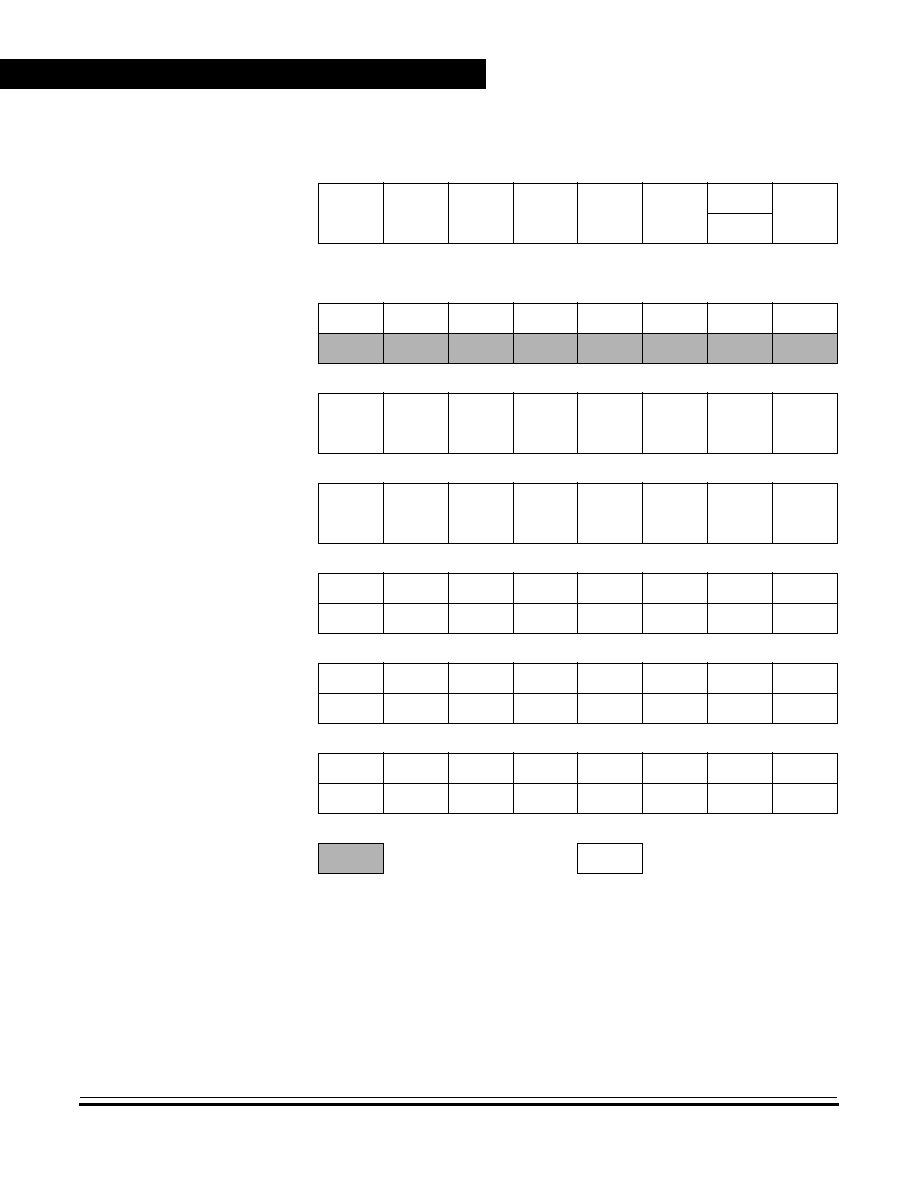
System Integration Module (SIM)
Technical Data
MC68H(R)C08JL3
--
Rev. 4
68
System Integration Module (SIM)
MOTOROLA
Addr.
Register Name
Bit 7
6
5
4
3
2
1
Bit 0
$FE00
Break Status Register
(BSR)
Read:
R
R
R
R
R
R
SBSW
R
Write:
NOTE
Reset:
0
0
0
0
0
0
0
0
Note: Writing a logic 0 clears SBSW.
$FE01
Reset Status Register
(RSR)
Read:
POR
PIN
COP
ILOP
ILAD
MODRST
LVI
0
Write:
POR:
1
0
0
0
0
0
0
0
$FE02
Reserved
Read:
R
R
R
R
R
R
R
R
Write:
Reset:
$FE03
Break Flag Control
Register
(BFCR)
Read:
BCFE
R
R
R
R
R
R
R
Write:
Reset:
0
$FE04
Interrupt Status Register 1
(INT1)
Read:
0
IF5
IF4
IF3
0
IF1
0
0
Write:
R
R
R
R
R
R
R
R
Reset:
0
0
0
0
0
0
0
0
$FE05
Interrupt Status Register 2
(INT2)
Read:
IF14
0
0
0
0
0
0
0
Write:
R
R
R
R
R
R
R
R
Reset:
0
0
0
0
0
0
0
0
$FE06
Interrupt Status Register 3
(INT3)
Read:
0
0
0
0
0
0
0
IF15
Write:
R
R
R
R
R
R
R
R
Reset:
0
0
0
0
0
0
0
0
= Unimplemented
R
= Reserved
Figure 7-2. SIM I/O Register Summary
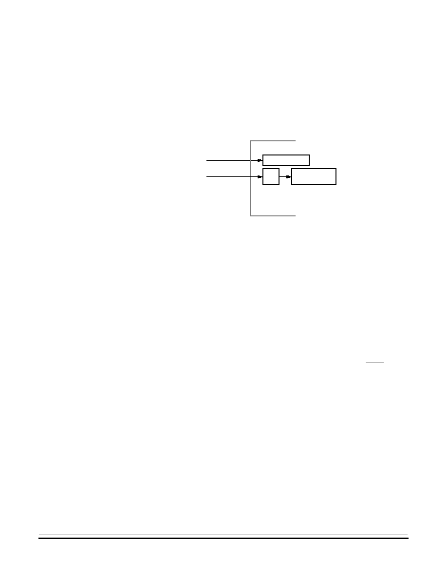
System Integration Module (SIM)
SIM Bus Clock Control and Generation
MC68H(R)C08JL3
--
Rev. 4
Technical Data
MOTOROLA
System Integration Module (SIM)
69
7.3 SIM Bus Clock Control and Generation
The bus clock generator provides system clock signals for the CPU and
peripherals on the MCU. The system clocks are generated from an
incoming clock, OSCOUT, as shown in
Figure 7-3
.
Figure 7-3. SIM Clock Signals
7.3.1 Bus Timing
In user mode, the internal bus frequency is the oscillator frequency
(2OSCOUT) divided by four.
7.3.2 Clock Start-Up from POR
When the power-on reset module generates a reset, the clocks to the
CPU and peripherals are inactive and held in an inactive phase until after
the 4096 2OSCOUT cycle POR time-out has completed. The RST pin is
driven low by the SIM during this entire period. The IBUS clocks start
upon completion of the time-out.
7.3.3 Clocks in Stop Mode and Wait Mode
Upon exit from stop mode by an interrupt, break, or reset, the SIM allows
2OSCOUT to clock the SIM counter. The CPU and peripheral clocks do
not become active until after the stop delay time-out. This time-out is
selectable as 4096 or 32 2OSCOUT cycles. (See
7.7.2 Stop Mode
.)
˜
2
BUS CLOCK
GENERATORS
SIM
SIM COUNTER
From
OSCILLATOR
From
OSCILLATOR
OSCOUT
2OSCOUT

System Integration Module (SIM)
Technical Data
MC68H(R)C08JL3
--
Rev. 4
70
System Integration Module (SIM)
MOTOROLA
In wait mode, the CPU clocks are inactive. The SIM also produces two
sets of clocks for other modules. Refer to the wait mode subsection of
each module to see if the module is active or inactive in wait mode.
Some modules can be programmed to be active in wait mode.
7.4 Reset and System Initialization
The MCU has these reset sources:
∑
Power-on reset module (POR)
∑
External reset pin (RST)
∑
Computer operating properly module (COP)
∑
Low-voltage inhibit module (LVI)
∑
Illegal opcode
∑
Illegal address
All of these resets produce the vector $FFFE≠FFFF ($FEFE≠FEFF in
Monitor mode) and assert the internal reset signal (IRST). IRST causes
all registers to be returned to their default values and all modules to be
returned to their reset states.
An internal reset clears the SIM counter (see
7.5 SIM Counter
), but an
external reset does not. Each of the resets sets a corresponding bit in
the reset status register (RSR). (See
7.8 SIM Registers
.)
7.4.1 External Pin Reset
The RST pin circuits include an internal pull-up device. Pulling the
asynchronous RST pin low halts all processing. The PIN bit of the reset
status register (RSR) is set as long as RST is held low for a minimum of
67 2OSCCLK cycles, assuming that the POR was not the source of the
reset. See
Table 7-2
for details.
Figure 7-4
shows the relative timing.
Table 7-2. PIN Bit Set Timing
Reset Type
Number of Cycles Required to Set PIN
POR
4163 (4096 + 64 + 3)
All others
67 (64 + 3)
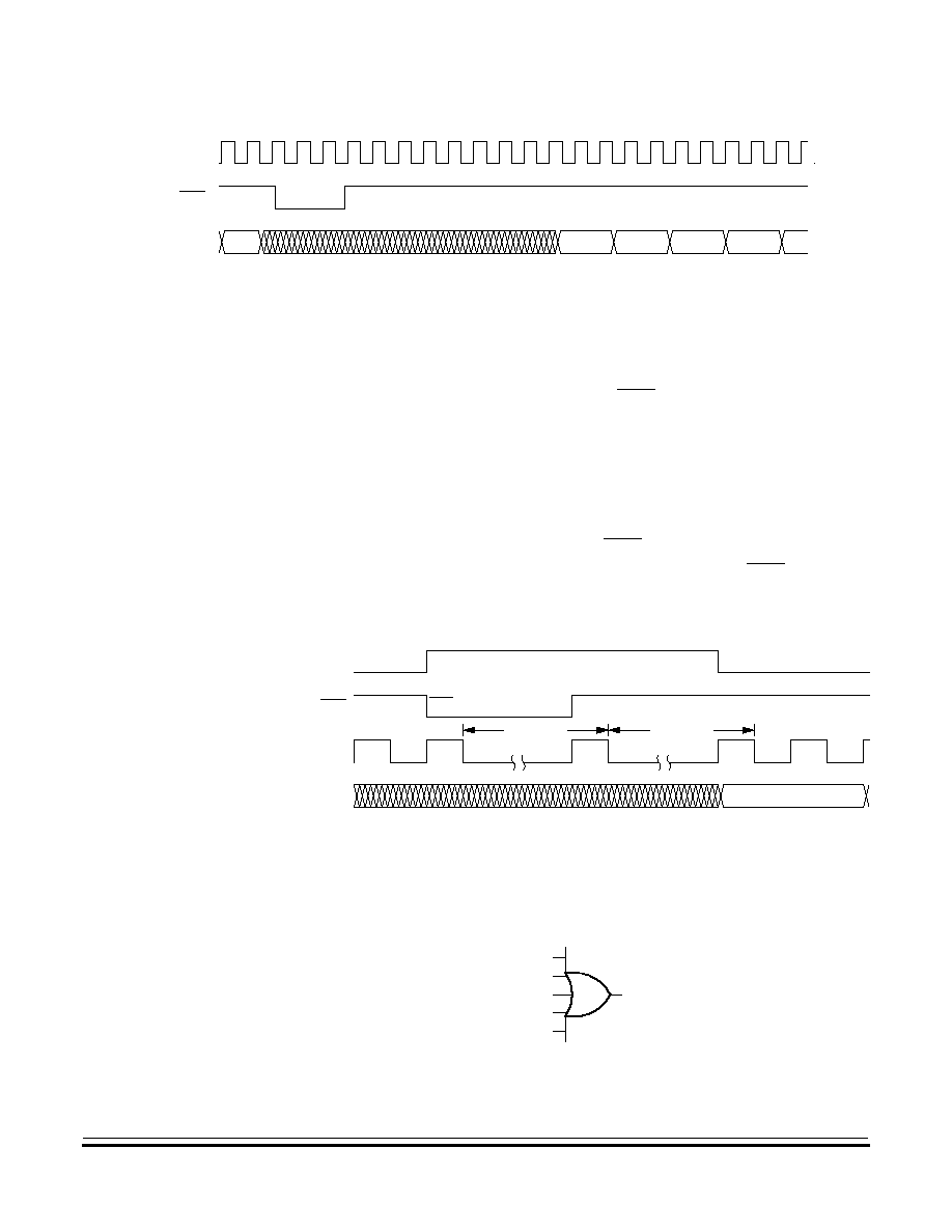
System Integration Module (SIM)
Reset and System Initialization
MC68H(R)C08JL3
--
Rev. 4
Technical Data
MOTOROLA
System Integration Module (SIM)
71
Figure 7-4. External Reset Timing
7.4.2 Active Resets from Internal Sources
All internal reset sources actively pull the RST pin low for 32 2OSCOUT
cycles to allow resetting of external peripherals. The internal reset signal
IRST continues to be asserted for an additional 32 cycles (
Figure 7-5
).
An internal reset can be caused by an illegal address, illegal opcode,
COP time-out, or POR. (See
Figure 7-6 . Sources of Internal Reset
.)
Note that for POR resets, the SIM cycles through 4096 2OSCOUT
cycles during which the SIM forces the RST pin low. The internal reset
signal then follows the sequence from the falling edge of RST shown in
Figure 7-5
.
Figure 7-5. Internal Reset Timing
The COP reset is asynchronous to the bus clock.
Figure 7-6. Sources of Internal Reset
RST
IAB
PC
VECT H VECT L
OSCOUT
IRST
RST
RST PULLED LOW BY MCU
IAB
32 CYCLES
32 CYCLES
VECTOR HIGH
2OSCOUT
ILLEGAL ADDRESS RST
ILLEGAL OPCODE RST
COPRST
POR
LVI
INTERNAL RESET
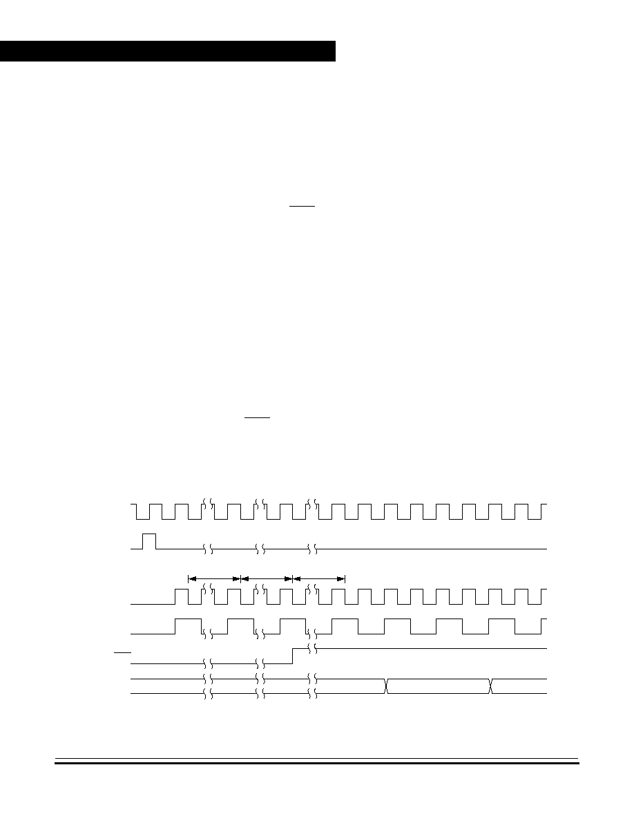
System Integration Module (SIM)
Technical Data
MC68H(R)C08JL3
--
Rev. 4
72
System Integration Module (SIM)
MOTOROLA
The active reset feature allows the part to issue a reset to peripherals
and other chips within a system built around the MCU.
7.4.2.1 Power-On Reset
When power is first applied to the MCU, the power-on reset module
(POR) generates a pulse to indicate that power-on has occurred. The
external reset pin (RST) is held low while the SIM counter counts out
4096 2OSCOUT cycles. Sixty-four 2OSCOUT cycles later, the CPU and
memories are released from reset to allow the reset vector sequence to
occur.
At power-on, the following events occur:
∑
A POR pulse is generated.
∑
The internal reset signal is asserted.
∑
The SIM enables the oscillator to drive 2OSCOUT.
∑
Internal clocks to the CPU and modules are held inactive for 4096
2OSCOUT cycles to allow stabilization of the oscillator.
∑
The RST pin is driven low during the oscillator stabilization time.
∑
The POR bit of the reset status register (RSR) is set and all other
bits in the register are cleared.
Figure 7-7. POR Recovery
PORRST
OSC1
2OSCOUT
OSCOUT
RST
IAB
4096
CYCLES
32
CYCLES
32
CYCLES
$FFFE
$FFFF

System Integration Module (SIM)
Reset and System Initialization
MC68H(R)C08JL3
--
Rev. 4
Technical Data
MOTOROLA
System Integration Module (SIM)
73
7.4.2.2 Computer Operating Properly (COP) Reset
An input to the SIM is reserved for the COP reset signal. The overflow of
the COP counter causes an internal reset and sets the COP bit in the
reset status register (RSR). The SIM actively pulls down the RST pin for
all internal reset sources.
To prevent a COP module time-out, write any value to location $FFFF.
Writing to location $FFFF clears the COP counter and stages 12 through
5 of the SIM counter. The SIM counter output, which occurs at least
every (2
12
≠ 2
4
) 2OSCOUT cycles, drives the COP counter. The COP
should be serviced as soon as possible out of reset to guarantee the
maximum amount of time before the first time-out.
The COP module is disabled if the RST pin or the IRQ1 pin is held at
V
DD
+ V
HI
while the MCU is in monitor mode. The COP module can be
disabled only through combinational logic conditioned with the high
voltage signal on the RST or the IRQ1 pin. This prevents the COP from
becoming disabled as a result of external noise. During a break state,
V
DD
+ V
HI
on the RST pin disables the COP module.
7.4.2.3 Illegal Opcode Reset
The SIM decodes signals from the CPU to detect illegal instructions. An
illegal instruction sets the ILOP bit in the reset status register (RSR) and
causes a reset.
If the stop enable bit, STOP, in the mask option register is logic zero, the
SIM treats the STOP instruction as an illegal opcode and causes an
illegal opcode reset. The SIM actively pulls down the RST pin for all
internal reset sources.
7.4.2.4 Illegal Address Reset
An opcode fetch from an unmapped address generates an illegal
address reset. The SIM verifies that the CPU is fetching an opcode prior
to asserting the ILAD bit in the reset status register (RSR) and resetting
the MCU. A data fetch from an unmapped address does not generate a
reset. The SIM actively pulls down the RST pin for all internal reset
sources.

System Integration Module (SIM)
Technical Data
MC68H(R)C08JL3
--
Rev. 4
74
System Integration Module (SIM)
MOTOROLA
7.4.2.5 LVI Reset
The low-voltage inhibit module (LVI) asserts its output to the SIM when
the V
DD
voltage falls to the LVI trip voltage V
TRIP
. The LVI bit in the SIM
reset status register (SRSR) is set, and the external reset pin (RSTB) is
held low while the SIM counter counts out 4096 2OSCCLK cycles. Sixty-
four 2OSCOUT cycles later, the CPU and memories are released from
reset to allow the reset vector sequence to occur. The SIM actively pulls
down the (RSTB) pin for all internal reset sources.
7.5 SIM Counter
The SIM counter is used by the power-on reset module (POR) and in
stop mode recovery to allow the oscillator time to stabilize before
enabling the internal bus (IBUS) clocks. The SIM counter also serves as
a prescaler for the computer operating properly module (COP). The SIM
counter uses 12 stages for counting, followed by a 13th stage that
triggers a reset of SIM counters and supplies the clock for the COP
module. The SIM counter is clocked by the falling edge of 2OSCOUT.
7.5.1 SIM Counter During Power-On Reset
The power-on reset module (POR) detects power applied to the MCU.
At power-on, the POR circuit asserts the signal PORRST. Once the SIM
is initialized, it enables the oscillator to drive the bus clock state machine.
7.5.2 SIM Counter During Stop Mode Recovery
The SIM counter also is used for stop mode recovery. The STOP
instruction clears the SIM counter. After an interrupt, break, or reset, the
SIM senses the state of the short stop recovery bit, SSREC, in the mask
option register. If the SSREC bit is a logic one, then the stop recovery is
reduced from the normal delay of 4096 2OSCOUT cycles down to 32
2OSCOUT cycles. This is ideal for applications using canned oscillators
that do not require long start-up times from stop mode. External crystal
applications should use the full stop recovery time, that is, with SSREC
cleared in the configuration register (CONFIG).

System Integration Module (SIM)
Exception Control
MC68H(R)C08JL3
--
Rev. 4
Technical Data
MOTOROLA
System Integration Module (SIM)
75
7.5.3 SIM Counter and Reset States
External reset has no effect on the SIM counter. (See
7.7.2 Stop Mode
for details.) The SIM counter is free-running after all reset states. (See
7.4.2 Active Resets from Internal Sources
for counter control and
internal reset recovery sequences.)
7.6 Exception Control
Normal, sequential program execution can be changed in three different
ways:
∑
Interrupts
≠
Maskable hardware CPU interrupts
≠
Non-maskable software interrupt instruction (SWI)
∑
Reset
∑
Break interrupts
7.6.1 Interrupts
An interrupt temporarily changes the sequence of program execution to
respond to a particular event.
Figure 7-8
flow charts the handling of
system interrupts.
Interrupts are latched, and arbitration is performed in the SIM at the start
of interrupt processing. The arbitration result is a constant that the CPU
uses to determine which vector to fetch. Once an interrupt is latched by
the SIM, no other interrupt can take precedence, regardless of priority,
until the latched interrupt is serviced (or the I bit is cleared).
System Integration Module (SIM)
Technical Data
MC68H(R)C08JL3
--
Rev. 4
76
System Integration Module (SIM)
MOTOROLA
Figure 7-8. Interrupt Processing
NO
NO
NO
YES
NO
NO
YES
NO
YES
YES
(As many interrupts as exist on chip)
I BIT SET?
FROM RESET
BREAK INTERRUPT?
I BIT SET?
IRQ
INTERRUPT?
TIMER
INTERRUPT?
SWI
INSTRUCTION?
RTI
INSTRUCTION?
FETCH NEXT
INSTRUCTION
UNSTACK CPU REGISTERS.
STACK CPU REGISTERS.
SET I BIT.
LOAD PC WITH INTERRUPT VECTOR.
EXECUTE INSTRUCTION.
YES
YES
System Integration Module (SIM)
Exception Control
MC68H(R)C08JL3
--
Rev. 4
Technical Data
MOTOROLA
System Integration Module (SIM)
77
At the beginning of an interrupt, the CPU saves the CPU register
contents on the stack and sets the interrupt mask (I bit) to prevent
additional interrupts. At the end of an interrupt, the RTI instruction
recovers the CPU register contents from the stack so that normal
processing can resume.
Figure 7-9
shows interrupt entry timing.
Figure
7-10
shows interrupt recovery timing.
Figure 7-9
.
Interrupt Entry
Figure 7-10. Interrupt Recovery
7.6.1.1 Hardware Interrupts
A hardware interrupt does not stop the current instruction. Processing of
a hardware interrupt begins after completion of the current instruction.
When the current instruction is complete, the SIM checks all pending
hardware interrupts. If interrupts are not masked (I bit clear in the
condition code register), and if the corresponding interrupt enable bit is
MODULE
IDB
R/W
INTERRUPT
DUMMY
SP
SP ≠ 1
SP ≠ 2
SP ≠ 3
SP ≠ 4
VECT H
VECT L
START ADDR
IAB
DUMMY
PC ≠ 1[7:0] PC ≠ 1[15:8]
X
A
CCR
V DATA H
V DATA L
OPCODE
I BIT
MODULE
IDB
R/W
INTERRUPT
SP ≠ 4
SP ≠ 3
SP ≠ 2
SP ≠ 1
SP
PC
PC + 1
IAB
CCR
A
X
PC ≠ 1[7:0] PC ≠ 1[15:8] OPCODE
OPERAND
I BIT

System Integration Module (SIM)
Technical Data
MC68H(R)C08JL3
--
Rev. 4
78
System Integration Module (SIM)
MOTOROLA
set, the SIM proceeds with interrupt processing; otherwise, the next
instruction is fetched and executed.
If more than one interrupt is pending at the end of an instruction
execution, the highest priority interrupt is serviced first.
Figure 7-11
demonstrates what happens when two interrupts are pending. If an
interrupt is pending upon exit from the original interrupt service routine,
the pending interrupt is serviced before the LDA instruction is executed.
Figure 7-11
.
Interrupt Recognition Example
The LDA opcode is prefetched by both the INT1 and INT2 RTI
instructions. However, in the case of the INT1 RTI prefetch, this is a
redundant operation.
NOTE:
To maintain compatibility with the M6805 Family, the H register is not
pushed on the stack during interrupt entry. If the interrupt service routine
modifies the H register or uses the indexed addressing mode, software
should save the H register and then restore it prior to exiting the routine.
CLI
LDA
INT1
PULH
RTI
INT2
BACKGROUND ROUTINE
#$FF
PSHH
INT1 INTERRUPT SERVICE ROUTINE
PULH
RTI
PSHH
INT2 INTERRUPT SERVICE ROUTINE
System Integration Module (SIM)
Exception Control
MC68H(R)C08JL3
--
Rev. 4
Technical Data
MOTOROLA
System Integration Module (SIM)
79
7.6.1.2 SWI Instruction
The SWI instruction is a non-maskable instruction that causes an
interrupt regardless of the state of the interrupt mask (I bit) in the
condition code register.
NOTE:
A software interrupt pushes PC onto the stack. A software interrupt does
not push PC ≠ 1, as a hardware interrupt does.
7.6.2 Interrupt Status Registers
The flags in the interrupt status registers identify maskable interrupt
sources.
Table 7-3
summarizes the interrupt sources and the interrupt
status register flags that they set. The interrupt status registers can be
useful for debugging.
Table 7-3. Interrupt Sources
Priority
Source
Flag
Mask
1
INT
Register
Flag
Vector Address
Highest
Reset
--
--
--
$FFFE≠$FFFF
SWI Instruction
--
--
--
$FFFC≠$FFFD
IRQ1 Pin
IRQF1
IMASK1
IF1
$FFFA≠$FFFB
Timer Channel 0 Interrupt
CH0F
CH0IE
IF3
$FFF6≠$FFF7
Timer Channel 1 Interrupt
CH1F
CH1IE
IF4
$FFF4≠$FFF5
Timer Overflow Interrupt
TOF
TOIE
IF5
$FFF2≠$FFF3
Keyboard Interrupt
KEYF
IMASKK
IF14
$FFE0≠$FFE1
Lowest
ADC Conversion Complete Interrupt
COCO
AIEN
IF15
$FFDE≠$FFDF
Note:
1. The I bit in the condition code register is a global mask for all interrupts sources except the SWI
instruction.

System Integration Module (SIM)
Technical Data
MC68H(R)C08JL3
--
Rev. 4
80
System Integration Module (SIM)
MOTOROLA
7.6.2.1 Interrupt Status Register 1
I
F
1, I
F
3 to IF5 -- Interrupt Flags
These flags indicate the presence of interrupt requests from the
sources shown in
Table 7-3
.
1 = Interrupt request present
0 = No interrupt request present
Bit 0, 1, 3 and 7 -- Always read 0
7.6.2.2 Interrupt Status Register 2
I
F
14 -- Interrupt Flags
This flag indicates the presence of interrupt requests from the sources
shown in
Table 7-3
.
1 = Interrupt request present
0 = No interrupt request present
Bit 0 to 6 -- Always read 0
Address:
$FE04
Bit 7
6
5
4
3
2
1
Bit 0
Read:
0
IF5
IF4
IF3
0
IF1
0
0
Write:
R
R
R
R
R
R
R
R
Reset:
0
0
0
0
0
0
0
0
R
= Reserved
Figure 7-12. Interrupt Status Register 1 (INT1)
Address:
$FE05
Bit 7
6
5
4
3
2
1
Bit 0
Read:
IF14
0
0
0
0
0
0
0
Write:
R
R
R
R
R
R
R
R
Reset:
0
0
0
0
0
0
0
0
R
= Reserved
Figure 7-13. Interrupt Status Register 2 (INT2)

System Integration Module (SIM)
Exception Control
MC68H(R)C08JL3
--
Rev. 4
Technical Data
MOTOROLA
System Integration Module (SIM)
81
7.6.2.3 Interrupt Status Register 3
I
F
15 -- Interrupt Flags
These flags indicate the presence of interrupt requests from the
sources shown in
Table 7-3
.
1 = Interrupt request present
0 = No interrupt request present
Bit 1 to 7 -- Always read 0
7.6.3 Reset
All reset sources always have equal and highest priority and cannot be
arbitrated.
7.6.4 Break Interrupts
The break module can stop normal program flow at a software-
programmable break point by asserting its break interrupt output. (See
Section 17. Break Module (BREAK)
.) The SIM puts the CPU into the
break state by forcing it to the SWI vector location. Refer to the break
interrupt subsection of each module to see how each module is affected
by the break state.
7.6.5 Status Flag Protection in Break Mode
The SIM controls whether status flags contained in other modules can
be cleared during break mode. The user can select whether flags are
Address:
$FE06
Bit 7
6
5
4
3
2
1
Bit 0
Read:
0
0
0
0
0
0
0
IF15
Write:
R
R
R
R
R
R
R
R
Reset:
0
0
0
0
0
0
0
0
R
= Reserved
Figure 7-14. Interrupt Status Register 3 (INT3)

System Integration Module (SIM)
Technical Data
MC68H(R)C08JL3
--
Rev. 4
82
System Integration Module (SIM)
MOTOROLA
protected from being cleared by properly initializing the break clear flag
enable bit (BCFE) in the break flag control register (BFCR).
Protecting flags in break mode ensures that set flags will not be cleared
while in break mode. This protection allows registers to be freely read
and written during break mode without losing status flag information.
Setting the BCFE bit enables the clearing mechanisms. Once cleared in
break mode, a flag remains cleared even when break mode is exited.
Status flags with a two-step clearing mechanism -- for example, a read
of one register followed by the read or write of another -- are protected,
even when the first step is accomplished prior to entering break mode.
Upon leaving break mode, execution of the second step will clear the
flag as normal.
7.7 Low-Power Modes
Executing the WAIT or STOP instruction puts the MCU in a low-power-
consumption mode for standby situations. The SIM holds the CPU in a
non-clocked state. The operation of each of these modes is described
below. Both STOP and WAIT clear the interrupt mask (I) in the condition
code register, allowing interrupts to occur.
7.7.1 Wait Mode
In wait mode, the CPU clocks are inactive while the peripheral clocks
continue to run.
Figure 7-15
shows the timing for wait mode entry.
A module that is active during wait mode can wake up the CPU with an
interrupt if the interrupt is enabled. Stacking for the interrupt begins one
cycle after the WAIT instruction during which the interrupt occurred. In
wait mode, the CPU clocks are inactive. Refer to the wait mode
subsection of each module to see if the module is active or inactive in
wait mode. Some modules can be programmed to be active in wait
mode.
Wait mode can also be exited by a reset or break. A break interrupt
during wait mode sets the SIM break stop/wait bit, SBSW, in the break
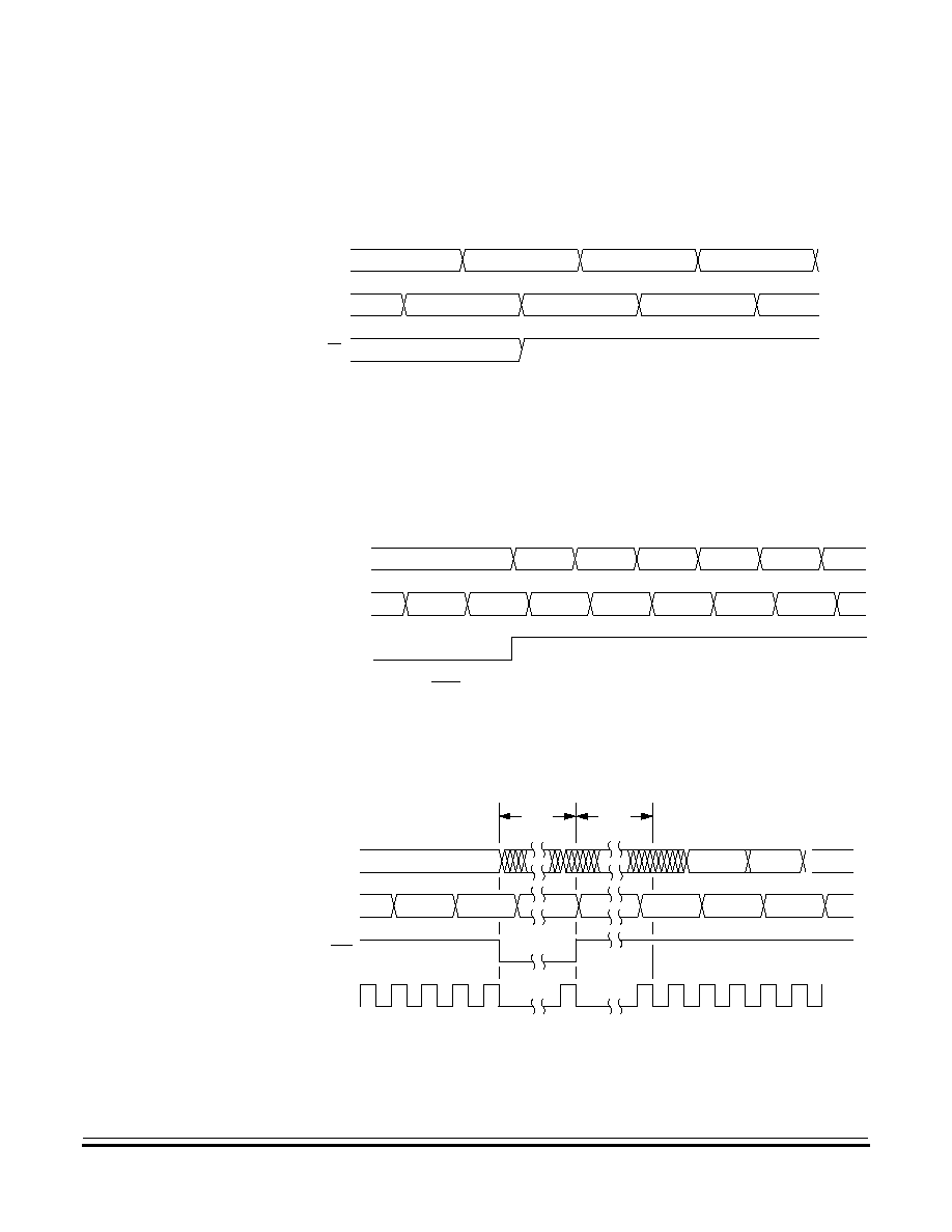
System Integration Module (SIM)
Low-Power Modes
MC68H(R)C08JL3
--
Rev. 4
Technical Data
MOTOROLA
System Integration Module (SIM)
83
status register (BSR). If the COP disable bit, COPD, in the mask option
register is logic zero, then the computer operating properly module
(COP) is enabled and remains active in wait mode.
Figure 7-15. Wait Mode Entry Timing
Figure 7-16
and
Figure 7-17
show the timing for WAIT recovery.
Figure 7-16. Wait Recovery from Interrupt or Break
Figure 7-17. Wait Recovery from Internal Reset
WAIT ADDR + 1
SAME
SAME
IAB
IDB
PREVIOUS DATA
NEXT OPCODE
SAME
WAIT ADDR
SAME
R/W
NOTE: Previous data can be operand data or the WAIT opcode, depending on the
last instruction.
$6E0C
$6E0B
$00FF
$00FE
$00FD
$00FC
$A6
$A6
$01
$0B
$6E
$A6
IAB
IDB
EXITSTOPWAIT
NOTE: EXITSTOPWAIT =
RST
pin OR CPU interrupt OR break interrupt
IAB
IDB
RST
$A6
$A6
$6E0B
RST VCT H
RST VCT L
$A6
2OSCOUT
32
Cycles
32
Cycles

System Integration Module (SIM)
Technical Data
MC68H(R)C08JL3
--
Rev. 4
84
System Integration Module (SIM)
MOTOROLA
7.7.2 Stop Mode
In stop mode, the SIM counter is reset and the system clocks are
disabled. An interrupt request from a module can cause an exit from stop
mode. Stacking for interrupts begins after the selected stop recovery
time has elapsed. Reset or break also causes an exit from stop mode.
The SIM disables the oscillator signals (OSCOUT and 2OSCOUT) in
stop mode, stopping the CPU and peripherals. Stop recovery time is
selectable using the SSREC bit in the configuration register (CONFIG).
If SSREC is set, stop recovery is reduced from the normal delay of 4096
2OSCOUT cycles down to 32. This is ideal for applications using canned
oscillators that do not require long start-up times from stop mode.
NOTE:
External crystal applications should use the full stop recovery time by
clearing the SSREC bit.
A break interrupt during stop mode sets the SIM break stop/wait bit
(SBSW) in the break status register (BSR).
The SIM counter is held in reset from the execution of the STOP
instruction until the beginning of stop recovery. It is then used to time the
recovery period.
Figure 7-18
shows stop mode entry timing.
NOTE:
To minimize stop current, all pins configured as inputs should be driven
to a logic 1 or logic 0.
Figure 7-18. Stop Mode Entry Timing
STOP ADDR + 1
SAME
SAME
IAB
IDB
PREVIOUS DATA
NEXT OPCODE
SAME
STOP ADDR
SAME
R/W
CPUSTOP
NOTE: Previous data can be operand data or the STOP opcode, depending on the last
instruction.
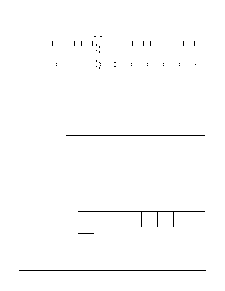
System Integration Module (SIM)
SIM Registers
MC68H(R)C08JL3
--
Rev. 4
Technical Data
MOTOROLA
System Integration Module (SIM)
85
Figure 7-19. Stop Mode Recovery from Interrupt or Break
7.8 SIM Registers
The SIM has three memory mapped registers.
Table 7-4
shows the
mapping of these registers.
7.8.1 Break Status Register (BSR)
The break status register contains a flag to indicate that a break caused
an exit from stop or wait mode.
2OSCOUT
INT/BREAK
IAB
STOP + 2
STOP + 2
SP
SP ≠ 1
SP ≠ 2
SP ≠ 3
STOP +1
STOP RECOVERY PERIOD
Table 7-4. SIM Registers
Address
Register
Access Mode
$FE00
BSR
User
$FE01
RSR
User
$FE03
BFCR
User
Address:
$FE00
Bit 7
6
5
4
3
2
1
Bit 0
Read:
R
R
R
R
R
R
SBSW
R
Write:
Note
(1)
Reset:
0
R
= Reserved
1. Writing a logic zero clears SBSW.
Figure 7-20. Break Status Register (BSR)

System Integration Module (SIM)
Technical Data
MC68H(R)C08JL3
--
Rev. 4
86
System Integration Module (SIM)
MOTOROLA
SBSW -- SIM Break Stop/Wait
This status bit is useful in applications requiring a return to wait or stop
mode after exiting from a break interrupt. Clear SBSW by writing a
logic zero to it. Reset clears SBSW.
1 = Stop mode or wait mode was exited by break interrupt
0 = Stop mode or wait mode was not exited by break interrupt
SBSW can be read within the break state SWI routine. The user can
modify the return address on the stack by subtracting one from it. The
following code is an example of this. Writing zero to the SBSW bit clears
it.
7.8.2 Reset Status Register (RSR)
This register contains six flags that show the source of the last reset.
Clear the SIM reset status register by reading it. A power-on reset sets
the POR bit and clears all other bits in the register.
;
;
;
This code works if the H register has been pushed onto the stack in the break
service routine software. This code should be executed at the end of the
break service routine software.
HIBYTE
EQU
5
LOBYTE
EQU
6
;
If not SBSW, do RTI
BRCLR
SBSW,BSR, RETURN
;
;
See if wait mode or stop mode was exited
by break.
TST
LOBYTE,SP
; If RETURNLO is not zero,
BNE
DOLO
; then just decrement low byte.
DEC
HIBYTE,SP
; Else deal with high byte, too.
DOLO
DEC
LOBYTE,SP
; Point to WAIT/STOP opcode.
RETURN
PULH
RTI
; Restore H register.

System Integration Module (SIM)
SIM Registers
MC68H(R)C08JL3
--
Rev. 4
Technical Data
MOTOROLA
System Integration Module (SIM)
87
POR -- Power-On Reset Bit
1 = Last reset caused by POR circuit
0 = Read of SRSR
PIN -- External Reset Bit
1 = Last reset caused by external reset pin (RST)
0 = POR or read of SRSR
COP -- Computer Operating Properly Reset Bit
1 = Last reset caused by COP counter
0 = POR or read of SRSR
ILOP -- Illegal Opcode Reset Bit
1 = Last reset caused by an illegal opcode
0 = POR or read of SRSR
ILAD -- Illegal Address Reset Bit (opcode fetches only)
1 = Last reset caused by an opcode fetch from an illegal address
0 = POR or read of SRSR
MODRST -- Monitor Mode Entry Module Reset bit
1 = Last reset caused by monitor mode entry when vector locations
$FFFE and $FFFF are $00 after POR while IRQB = V
DD
0 = POR or read of SRSR
LVI -- Low Voltage Inhibit Reset bit
1 = Last reset caused by LVI circuit
0 = POR or read of SRSR
Address:
$FE01
Bit 7
6
5
4
3
2
1
Bit 0
Read:
POR
PIN
COP
ILOP
ILAD
MODRST
LVI
0
Write:
POR:
1
0
0
0
0
0
0
0
= Unimplemented
Figure 7-21. Reset Status Register (RSR)

System Integration Module (SIM)
Technical Data
MC68H(R)C08JL3
--
Rev. 4
88
System Integration Module (SIM)
MOTOROLA
7.8.3 Break Flag Control Register (BFCR)
The break control register contains a bit that enables software to clear
status bits while the MCU is in a break state.
BCFE -- Break Clear Flag Enable Bit
This read/write bit enables software to clear status bits by accessing
status registers while the MCU is in a break state. To clear status bits
during the break state, the BCFE bit must be set.
1 = Status bits clearable during break
0 = Status bits not clearable during break
Address:
$FE03
Bit 7
6
5
4
3
2
1
Bit 0
Read:
BCFE
R
R
R
R
R
R
R
Write:
Reset:
0
R
= Reserved
Figure 7-22. Break Flag Control Register (BFCR)

MC68H(R)C08JL3
--
Rev. 4
Technical Data
MOTOROLA
Oscillator (OSC)
89
Technical Data -- MC68H(R)C08JL3
Section 8. Oscillator (OSC)
8.1 Contents
8.2
Introduction . . . . . . . . . . . . . . . . . . . . . . . . . . . . . . . . . . . . . . . . 89
8.3
X-tal Oscillator (MC68HC08xxx). . . . . . . . . . . . . . . . . . . . . . . . 90
8.4
RC Oscillator (MC68HRC08xxx) . . . . . . . . . . . . . . . . . . . . . . . 91
8.5
I/O Signals . . . . . . . . . . . . . . . . . . . . . . . . . . . . . . . . . . . . . . . . 92
8.5.1
Crystal Amplifier Input Pin (OSC1). . . . . . . . . . . . . . . . . . . . 92
8.5.2
Crystal Amplifier Output Pin (OSC2/PTA6/RCCLK). . . . . . . 92
8.5.3
Oscillator Enable Signal (SIMOSCEN). . . . . . . . . . . . . . . . . 92
8.5.4
X-tal Oscillator Clock (XTALCLK). . . . . . . . . . . . . . . . . . . . . 92
8.5.5
RC Oscillator Clock (RCCLK). . . . . . . . . . . . . . . . . . . . . . . . 93
8.5.6
Oscillator Out 2 (2OSCOUT) . . . . . . . . . . . . . . . . . . . . . . . . 93
8.5.7
Oscillator Out (OSCOUT). . . . . . . . . . . . . . . . . . . . . . . . . . . 93
8.6
Low Power Modes . . . . . . . . . . . . . . . . . . . . . . . . . . . . . . . . . . 93
8.6.1
Wait Mode . . . . . . . . . . . . . . . . . . . . . . . . . . . . . . . . . . . . . . 93
8.6.2
Stop Mode . . . . . . . . . . . . . . . . . . . . . . . . . . . . . . . . . . . . . . 93
8.7
Oscillator During Break Mode. . . . . . . . . . . . . . . . . . . . . . . . . . 94
8.2 Introduction
The oscillator module provides the reference clock for the MCU system
and bus. Two types of oscillator modules are available:
∑
MC68HC08xxx-- built-in oscillator module (X-tal oscillator) that
requires an external crystal or ceramic-resonator. This option also
allows an external clock that can be driven directly into OSC1.
∑
MC68HRC08xxx -- built-in oscillator module (RC oscillator) that
requires an external RC connection only.
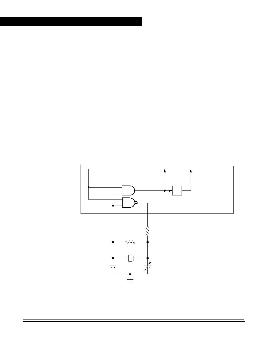
Oscillator (OSC)
Technical Data
MC68H(R)C08JL3
--
Rev. 4
90
Oscillator (OSC)
MOTOROLA
8.3 X-tal Oscillator (MC68HC08xxx)
The X-tal oscillator circuit is designed for use with an external crystal or
ceramic resonator to provide accurate clock source.
In its typical configuration, the X-tal oscillator is connected in a Pierce
oscillator configuration, as shown in
Figure 8-1
. This figure shows only
the logical representation of the internal components and may not
represent actual circuitry. The oscillator configuration uses five
components:
∑
Crystal, X
1
∑
Fixed capacitor, C
1
∑
Tuning capacitor, C
2
(can also be a fixed capacitor)
∑
Feedback resistor, R
B
∑
Series resistor, R
S
(optional)
Figure 8-1. X-tal Oscillator External Connections
C
1
C
2
SIMOSCEN
XTALCLK
R
B
X
1
R
S
*
*R
S
can be zero (shorted) when used with higher-frequency crystals.
MCU
From SIM
Refer to manufacturer's data.
OSC2
OSC1
˜ 2
OSCOUT
2OSCOUT
To SIM
To SIM
See
Section 18.
for component value requirements.
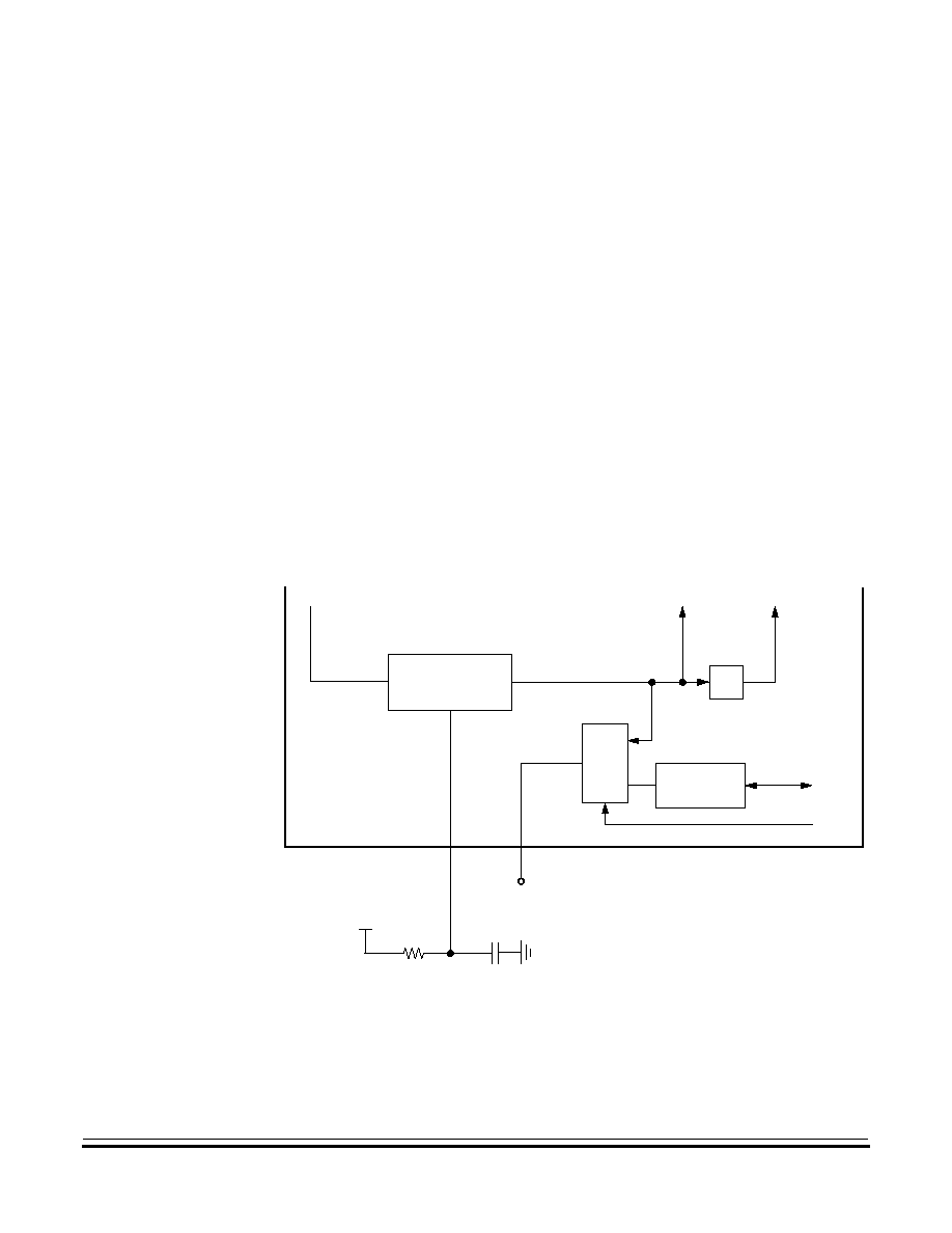
Oscillator (OSC)
RC Oscillator (MC68HRC08xxx)
MC68H(R)C08JL3
--
Rev. 4
Technical Data
MOTOROLA
Oscillator (OSC)
91
The series resistor (R
S
) is included in the diagram to follow strict Pierce
oscillator guidelines and may not be required for all ranges of operation,
especially with high frequency crystals. Refer to the crystal
manufacturer's data for more information.
8.4 RC Oscillator (MC68HRC08xxx)
The RC oscillator circuit is designed for use with external R and C to
provide a clock source with tolerance less than 10%.
In its typical configuration, the RC oscillator requires two external
components, one R and one C. Component values should have a
tolerance of 1% or less, to obtain a clock source with less than 10%
tolerance. The oscillator configuration uses two components:
∑
C
EXT
∑
R
EXT
Figure 8-2. RC Oscillator External Connections
MCU
R
EXT
C
EXT
SIMOSCEN
OSC1
Ext-RC
Oscillator
EN
RCCLK
˜ 2
OSCOUT
2OSCOUT
To SIM
From SIM
V
DD
PTA6
I/O
0
1
PTA6
PTA6EN
PTA6/RCCLK (OSC2)
To SIM
See
Section 18.
for component value requirements.

Oscillator (OSC)
Technical Data
MC68H(R)C08JL3
--
Rev. 4
92
Oscillator (OSC)
MOTOROLA
8.5 I/O Signals
The following paragraphs describe the oscillator I/O signals.
8.5.1 Crystal Amplifier Input Pin (OSC1)
OSC1 pin is an input to the crystal oscillator amplifier or the input to the
RC oscillator circuit.
8.5.2 Crystal Amplifier Output Pin (OSC2/PTA6/RCCLK)
For the X-tal oscillator device, OSC2 pin is the output of the crystal
oscillator inverting amplifier.
For the RC oscillator device, OSC2 pin can be configured as a general
purpose I/O pin PTA6, or the output of the internal RC oscillator clock,
RCCLK.
8.5.3 Oscillator Enable Signal (SIMOSCEN)
The SIMOSCEN signal comes from the system integration module (SIM)
and enables/disables the X-tal oscillator circuit or the RC-oscillator.
8.5.4 X-tal Oscillator Clock (XTALCLK)
XTALCLK is the X-tal oscillator output signal. It runs at the full speed of
the crystal (f
XCLK
) and comes directly from the crystal oscillator circuit.
Figure 8-1
shows only the logical relation of XTALCLK to OSC1 and
OSC2 and may not represent the actual circuitry. The duty cycle of
XTALCLK is unknown and may depend on the crystal and other external
factors. Also, the frequency and amplitude of XTALCLK can be unstable
at start-up.
Option
OSC2 pin function
X-tal oscillator
Inverting OSC1
RC oscillator
Controlled by PTAEN bit in PTAPUER ($0D)
PTA6EN = 0: RCCLK output
PTA6EN = 1: PTA6 I/O

Oscillator (OSC)
Low Power Modes
MC68H(R)C08JL3
--
Rev. 4
Technical Data
MOTOROLA
Oscillator (OSC)
93
8.5.5 RC Oscillator Clock (RCCLK)
RCCLK is the RC oscillator output signal. Its frequency is directly
proportional to the time constant of the external R and C.
Figure 8-2
shows only the logical relation of RCCLK to OSC1 and may not
represent the actual circuitry.
8.5.6 Oscillator Out 2 (2OSCOUT)
2OSCOUT is same as the input clock (XTALCLK or RCCLK). This signal
is driven to the SIM module and is used to determine the COP cycles.
8.5.7 Oscillator Out (OSCOUT)
The frequency of this signal is equal to half of the 2OSCOUT, this signal
is driven to the SIM for generation of the bus clocks used by the CPU
and other modules on the MCU. OSCOUT will be divided again in the
SIM and results in the internal bus frequency being one fourth of the
XTALCLK or RCCLK frequency.
8.6 Low Power Modes
The WAIT and STOP instructions put the MCU in low-power
consumption standby modes.
8.6.1 Wait Mode
The WAIT instruction has no effect on the oscillator logic. OSCOUT and
2OSCOUT continues to drive to the SIM module.
8.6.2 Stop Mode
The STOP instruction disables the XTALCLK or the RCCLK output,
hence OSCOUT and 2OSCOUT.

Oscillator (OSC)
Technical Data
MC68H(R)C08JL3
--
Rev. 4
94
Oscillator (OSC)
MOTOROLA
8.7 Oscillator During Break Mode
The oscillator continues to drive OSCOUT and 2OSCOUT when the
device enters the break state.

MC68H(R)C08JL3
--
Rev. 4
Technical Data
MOTOROLA
Monitor ROM (MON)
95
Technical Data -- MC68H(R)C08JL3
Section 9. Monitor ROM (MON)
9.1 Contents
9.2
Introduction . . . . . . . . . . . . . . . . . . . . . . . . . . . . . . . . . . . . . . . . 95
9.3
Features . . . . . . . . . . . . . . . . . . . . . . . . . . . . . . . . . . . . . . . . . . 96
9.4
Functional Description . . . . . . . . . . . . . . . . . . . . . . . . . . . . . . . 96
9.4.1
Entering Monitor Mode . . . . . . . . . . . . . . . . . . . . . . . . . . . . . 98
9.4.2
Baud Rate . . . . . . . . . . . . . . . . . . . . . . . . . . . . . . . . . . . . . 100
9.4.3
Data Format . . . . . . . . . . . . . . . . . . . . . . . . . . . . . . . . . . . . 100
9.4.4
Echoing . . . . . . . . . . . . . . . . . . . . . . . . . . . . . . . . . . . . . . . 100
9.4.5
Break Signal . . . . . . . . . . . . . . . . . . . . . . . . . . . . . . . . . . . . 101
9.4.6
Commands . . . . . . . . . . . . . . . . . . . . . . . . . . . . . . . . . . . . . 101
9.2 Introduction
This section describes the monitor ROM (MON). The monitor ROM
allows complete testing of the MCU through a single-wire interface with
a host computer.

Monitor ROM (MON)
Technical Data
MC68H(R)C08JL3
--
Rev. 4
96
Monitor ROM (MON)
MOTOROLA
9.3 Features
Features of the monitor ROM include the following:
∑
Normal user-mode pin functionality
∑
One pin dedicated to serial communication between monitor ROM
and host computer
∑
Standard mark/space non-return-to-zero (NRZ) communication
with host computer
∑
4800 Baud to 28.8 k-Baud communication with host computer
∑
Execution of code in RAM or ROM
9.4 Functional Description
The monitor ROM receives and executes commands from a host
computer.
Figure 9-1
shows a example circuit used to enter monitor
mode and communicate with a host computer via a standard RS-232
interface.
While simple monitor commands can access any memory address, the
MCU has a ROM security feature that requires proper procedures to be
followed before the ROM can be accessed. Access to the ROM is denied
to unauthorized users of customer-specified software.
In monitor mode, the MCU can execute host-computer code in RAM
while all MCU pins except PTB0 retain normal operating mode functions.
All communication between the host computer and the MCU is through
the PTB0 pin. A level-shifting and multiplexing interface is required
between PTB0 and the host computer. PTB0 is used in a wired-OR
configuration and requires a pull-up resistor.
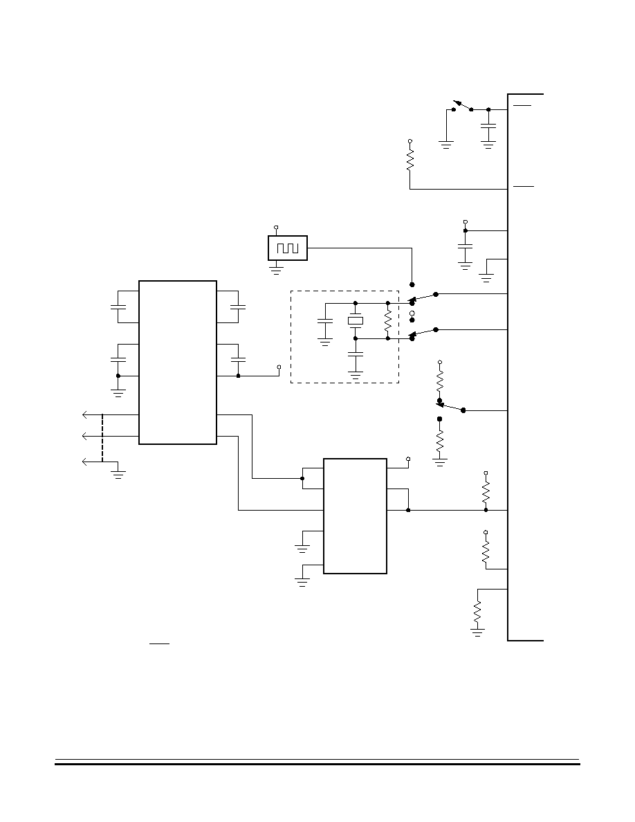
Monitor ROM (MON)
Functional Description
MC68H(R)C08JL3
--
Rev. 4
Technical Data
MOTOROLA
Monitor ROM (MON)
97
Figure 9-1. Monitor Mode Circuit
+
+
+
+
MC145407
MC74HC125
H(R)C08JL3
RST
IRQ1
OSC1
OSC2
V
SS
PTB0
V
DD
10 k
10k
6
5
2
4
3
1
DB-25
2
3
7
20
18
17
19
16
15
V
DD
V
DD
10
µ
F
10
µ
F
10
µ
F
10
µ
F
1
2
4
7
14
3
0.1
µ
F
5
6
PTB1
V
DD
0.1
µ
F
V
DD
PTB2
V
DD
10 k
PTB3
V
DD
10 k
10 k
10 k
SW1
A
B
V
DD
+ V
HI
NOTES:
1. SW1: Position A -- Bus clock = OSC1 clock ˜ 4
SW1: Position B -- Bus clock = OSC1 clock ˜ 2
2. See
Table 18-4
for IRQ1 voltage level requirements.
3. SW2: Position C-- External oscillator clock input
SW2: Position D-- Crystal oscillator clock input
External oscillator must have a 50% duty cycle
(SEE NOTE 1)
H(R)C08JK3
H(R)C08JK1
(SEE NOTE 2)
10
M
20 pF
20 pF
9.8304MHz
C
D
V
DD
(SEE NOTE 3)
C
D
X-TAL CIRCUIT
9.8304 MHz
SW2
Monitor ROM (MON)
Technical Data
MC68H(R)C08JL3
--
Rev. 4
98
Monitor ROM (MON)
MOTOROLA
9.4.1 Entering Monitor Mode
Table 9-1
shows the pin conditions for entering monitor mode. As
specified in the table, monitor mode may be entered after a POR and will
allow communication at 9600 baud provided one of the following sets of
conditions is met:
1. If IRQ1 = V
DD
+ V
HI
:
≠
OSC1 is 4.9125MHz
≠
PTB3 = low
2. If IRQ1 = V
DD
+ V
HI
:
≠
OSC1 is 9.8304MHz
≠
PTB3 = high
If V
DD
+V
HI
is applied to IRQ1 and PTB3 is low upon monitor mode entry
(
Table 9-1
condition set 1), the bus frequency is a divide-by-two of the
clock input to OSC1. If PTB3 is high with V
DD
+V
HI
applied to IRQ1 upon
monitor mode entry (
Table 9-1
condition set 2), the bus frequency is a
divide-by-four of the clock input to OSC1. Holding the PTB3 pin low
when entering monitor mode causes a bypass of a divide-by-two stage
at the internal clock circuit.
In this event, the OSCOUT frequency is
Table 9-1. Monitor Mode Entry Requirements and Options
IRQ
1
PTB3
PTB2
PTB1
PTB0
Clock Source
and
Frequency
Bus
Frequency
Comments
V
DD
+ V
HI
0
0
1
1
OSC1 at
4.9152MHz
2.4576MHz
Bypasses RC oscillator (in
HRC08xxx); OSC1 input
must be x-tal oscillator or
external oscillator clock.
9600 baud communication
on PTB0. COP disabled.
V
DD
+ V
HI
1
0
1
1
OSC1 at
9.8304MHz
2.4576MHz
V
DD
X
X
X
X
X-tal or RC
oscillator at
desired frequency
XTALCLK ˜ 4
or
RCCLK ˜ 4
Enters User mode
Notes:
1. PTB3 = 0: Bypasses the divide-by-two prescaler to SIM.
The OSC1 clock must be 50% duty cycle for this condition.
2. XTALCLK is the X-tal oscillator output, for MC68HC08xxx. See
Figure 8-1
.
4. RCCLK is the RC oscillator output, for MC68HRC08xxx. See
Figure 8-2
.
5. See
Table 18-4
for V
DD
+ V
HI
voltage level requirements.
Monitor ROM (MON)
Functional Description
MC68H(R)C08JL3
--
Rev. 4
Technical Data
MOTOROLA
Monitor ROM (MON)
99
equal to the 2OSCOUT frequency, and OSC1 input directly generates
internal bus clocks. In this case, the OSC1 signal must have a 50% duty
cycle at maximum bus frequency.
In monitor mode, the COP is disabled as long as V
DD
+ V
HI
is applied to
either the IRQ1 or the RST pin. (See
Section 7. System Integration
Module (SIM)
for more information on modes of operation.)
Enter monitor mode with the pin configuration shown above by pulling
RST low and then high. The rising edge of RST latches monitor mode.
Once monitor mode is latched, the values on the specified pins can
change.
Once out of reset, the MCU sends a break signal (10 consecutive logic
zeros) to the host computer, indicating that it is ready to receive a
command. The break signal also provides a timing reference to allow the
host to determine the necessary baud rate.
In monitor mode, the MCU uses different vectors for reset, SWI, and
break interrupt. The alternate vectors are in the $FE page instead of the
$FF page and allow code execution from the internal monitor firmware
instead of user code.
Table 9-2
is a summary of the vector differences between user mode
and monitor mode.
When the host computer has completed downloading code into the MCU
RAM, the host then sends a RUN command, which executes an RTI,
which sends control to the address on the stack pointer.
Table 9-2. Monitor Mode Vector Differences
Modes
Functions
COP
Reset
Vector
High
Reset
Vector
Low
Break
Vector
High
Break
Vector
Low
SWI
Vector
High
SWI
Vector
Low
User
Enabled
$FFFE
$FFFF
$FFFC
$FFFD
$FFFC
$FFFD
Monitor
Disabled
(1)
$FEFE
$FEFF
$FEFC
$FEFD
$FEFC
$FEFD
Notes:
1. If the high voltage (V
DD
+ V
HI
) is removed from the IRQ1 pin or the RST pin, the SIM
asserts its COP enable output. The COP is a mask option enabled or disabled by the
COPD bit in the configuration register.

Monitor ROM (MON)
Technical Data
MC68H(R)C08JL3
--
Rev. 4
100
Monitor ROM (MON)
MOTOROLA
9.4.2 Baud Rate
The communication baud rate is dependant on oscillator frequency and
the state of PTB3 upon monitor mode entry. When PTB3 is high, the
divide by ratio is 1024. If the PTB3 pin is at logic zero upon entry into
monitor mode, the divide by ratio is 512.
9.4.3 Data Format
Communication with the monitor ROM is in standard non-return-to-zero
(NRZ) mark/space data format. (See
Figure 9-2
and
Figure 9-3
.)
Figure 9-2. Monitor Data Format
Figure 9-3. Sample Monitor Waveforms
The data transmit and receive rate can be anywhere from 4800 baud to
28.8k-baud. Transmit and receive baud rates must be identical.
9.4.4 Echoing
As shown in
Figure 9-4
, the monitor ROM immediately echoes each
received byte back to the PTB0 pin for error checking.
Table 9-3. Monitor Baud Rate Selection
Oscillator Input Frequency
PTB3
Baud Rate
4.9152 MHz
0
9600 bps
9.8304 MHz
1
9600 bps
4.9152 MHz
1
4800 bps
BIT 5
START
BIT
BIT 0
BIT 1
NEXT
STOP
BIT
START
BIT
BIT 2
BIT 3
BIT 4
BIT 6
BIT 7
BIT 5
START
BIT
BIT 0
BIT 1
NEXT
STOP
BIT
START
BIT
BIT 2
BIT 3
BIT 4
BIT 6
BIT 7
START
BIT
BIT 0
BIT 1
NEXT
STOP
BIT
START
BIT
BIT 2
$A5
BREAK
BIT 3
BIT 4
BIT 5
BIT 6
BIT 7

Monitor ROM (MON)
Functional Description
MC68H(R)C08JL3
--
Rev. 4
Technical Data
MOTOROLA
Monitor ROM (MON)
101
Figure 9-4. Read Transaction
Any result of a command appears after the echo of the last byte of the
command.
9.4.5 Break Signal
A start bit followed by nine low bits is a break signal. (See
Figure 9-5.)
When the monitor receives a break signal, it drives the PTB0 pin high for
the duration of two bits before echoing the break signal.
Figure 9-5. Break Transaction
9.4.6 Commands
The monitor ROM uses the following commands:
∑
READ (read memory)
∑
WRITE (write memory)
∑
IREAD (indexed read)
∑
IWRITE (indexed write)
∑
READSP (read stack pointer)
∑
RUN (run user program)
ADDR. HIGH
READ
READ
ADDR. HIGH
ADDR. LOW
ADDR. LOW
DATA
ECHO
SENT TO
MONITOR
RESULT
0
1
2
3
4
5
6
7
0
1
2
3
4
5
6
7
MISSING STOP BIT
TWO-STOP-BIT DELAY BEFORE ZERO ECHO
Monitor ROM (MON)
Technical Data
MC68H(R)C08JL3
--
Rev. 4
102
Monitor ROM (MON)
MOTOROLA
Table 9-4. READ (Read Memory) Command
Description
Read byte from memory
Operand
Specifies 2-byte address in high byte:low byte order
Data Returned
Returns contents of specified address
Opcode
$4A
Command Sequence
ADDR. HIGH
READ
READ
ADDR. HIGH
ADDR. LOW
ADDR. LOW
DATA
ECHO
SENT TO
MONITOR
RESULT
Table 9-5. WRITE (Write Memory) Command
Description
Write byte to memory
Operand
Specifies 2-byte address in high byte:low byte order; low byte followed by data byte
Data Returned
None
Opcode
$49
Command Sequence
ADDR. HIGH
WRITE
WRITE
ADDR. HIGH
ADDR. LOW
ADDR. LOW
DATA
ECHO
SENT TO
MONITOR
DATA

Monitor ROM (MON)
Functional Description
MC68H(R)C08JL3
--
Rev. 4
Technical Data
MOTOROLA
Monitor ROM (MON)
103
NOTE:
A sequence of IREAD or IWRITE commands can sequentially access a
block of memory over the full 64-Kbyte memory map.
Table 9-6. IREAD (Indexed Read) Command
Description
Read next 2 bytes in memory from last address accessed
Operand
Specifies 2-byte address in high byte:low byte order
Data Returned
Returns contents of next two addresses
Opcode
$1A
Command Sequence
DATA
IREAD
IREAD
DATA
ECHO
SENT TO
MONITOR
RESULT
Table 9-7. IWRITE (Indexed Write) Command
Description
Write to last address accessed + 1
Operand
Specifies single data byte
Data Returned
None
Opcode
$19
Command Sequence
DATA
IWRITE
IWRITE
DATA
ECHO
SENT TO
MONITOR
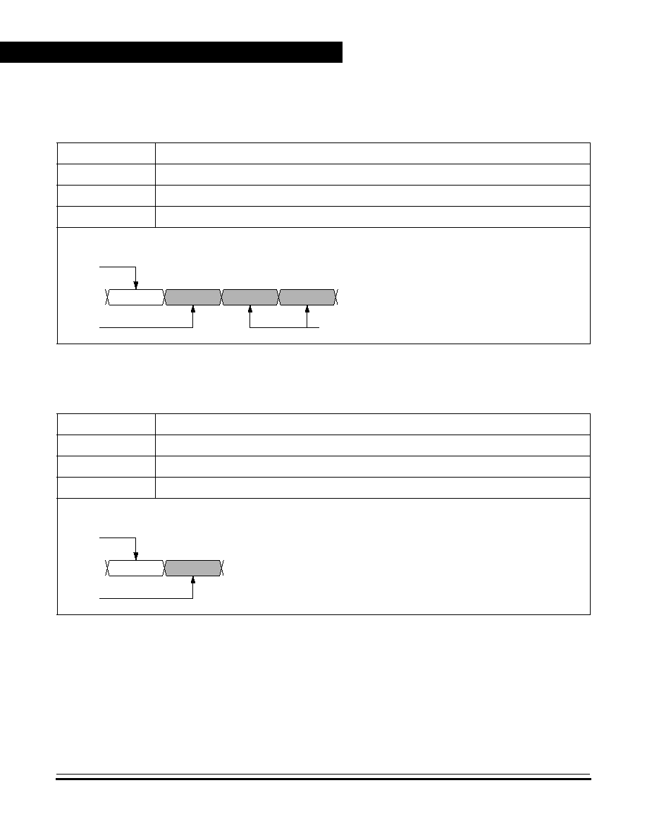
Monitor ROM (MON)
Technical Data
MC68H(R)C08JL3
--
Rev. 4
104
Monitor ROM (MON)
MOTOROLA
Table 9-8. READSP (Read Stack Pointer) Command
Description
Reads stack pointer
Operand
None
Data Returned
Returns stack pointer in high byte:low byte order
Opcode
$0C
Command Sequence
SP HIGH
READSP
READSP
SP LOW
ECHO
SENT TO
MONITOR
RESULT
Table 9-9. RUN (Run User Program) Command
Description
Executes RTI instruction
Operand
None
Data Returned
None
Opcode
$28
Command Sequence
RUN
RUN
ECHO
SENT TO
MONITOR

MC68H(R)C08JL3
--
Rev. 4
Technical Data
MOTOROLA
Timer Interface Module (TIM)
105
Technical Data -- MC68H(R)C08JL3
Section 10. Timer Interface Module (TIM)
10.1 Contents
10.2
Introduction . . . . . . . . . . . . . . . . . . . . . . . . . . . . . . . . . . . . . . . 106
10.3
Features . . . . . . . . . . . . . . . . . . . . . . . . . . . . . . . . . . . . . . . . . 106
10.4
Pin Name Conventions . . . . . . . . . . . . . . . . . . . . . . . . . . . . . . 106
10.5
Functional Description . . . . . . . . . . . . . . . . . . . . . . . . . . . . . . 107
10.5.1
TIM Counter Prescaler . . . . . . . . . . . . . . . . . . . . . . . . . . . . 109
10.5.2
Input Capture . . . . . . . . . . . . . . . . . . . . . . . . . . . . . . . . . . . 109
10.5.3
Output Compare. . . . . . . . . . . . . . . . . . . . . . . . . . . . . . . . . 109
10.5.3.1
Unbuffered Output Compare . . . . . . . . . . . . . . . . . . . . . 110
10.5.3.2
Buffered Output Compare . . . . . . . . . . . . . . . . . . . . . . . 110
10.5.4
Pulse Width Modulation (PWM) . . . . . . . . . . . . . . . . . . . . . 111
10.5.4.1
Unbuffered PWM Signal Generation . . . . . . . . . . . . . . . 112
10.5.4.2
Buffered PWM Signal Generation . . . . . . . . . . . . . . . . . 113
10.5.4.3
PWM Initialization . . . . . . . . . . . . . . . . . . . . . . . . . . . . . 114
10.6
Interrupts. . . . . . . . . . . . . . . . . . . . . . . . . . . . . . . . . . . . . . . . . 115
10.7
Wait Mode. . . . . . . . . . . . . . . . . . . . . . . . . . . . . . . . . . . . . . . . 115
10.8
TIM During Break Interrupts . . . . . . . . . . . . . . . . . . . . . . . . . . 116
10.9
I/O Signals . . . . . . . . . . . . . . . . . . . . . . . . . . . . . . . . . . . . . . . 116
10.10 I/O Registers. . . . . . . . . . . . . . . . . . . . . . . . . . . . . . . . . . . . . . 117
10.10.1 TIM Status and Control Register (TSC) . . . . . . . . . . . . . . . 117
10.10.2 TIM Counter Registers (TCNTH:TCNTL) . . . . . . . . . . . . . . 119
10.10.3 TIM Counter Modulo Registers (TMODH:TMODL) . . . . . . 120
10.10.4 TIM Channel Status and Control Registers (TSC0:TSC1) . 121
10.10.5 TIM Channel Registers (TCH0H/L:TCH1H/L) . . . . . . . . . . 125

Timer Interface Module (TIM)
Technical Data
MC68H(R)C08JL3
--
Rev. 4
106
Timer Interface Module (TIM)
MOTOROLA
10.2 Introduction
This section describes the timer interface module (TIM2, Version B). The
TIM is a two-channel timer that provides a timing reference with input
capture, output compare, and pulse-width-modulation functions.
Figure 10-1
is a block diagram of the TIM.
10.3 Features
Features of the TIM include the following:
∑
Two input capture/output compare channels
≠
Rising-edge, falling-edge, or any-edge input capture trigger
≠
Set, clear, or toggle output compare action
∑
Buffered and unbuffered pulse width modulation (PWM) signal
generation
∑
Programmable TIM clock input with 7-frequency internal bus clock
prescaler selection
∑
Free-running or modulo up-count operation
∑
Toggle any channel pin on overflow
∑
TIM counter stop and reset bits
∑
Modular architecture expandable to eight channels
10.4 Pin Name Conventions
The TIM share two I/O pins with two port D I/O pins. The full name of the
TIM I/O pins are listed in
Table 10-1
.
The generic pin name appear in the
text that follows.
Table 10-1. Pin Name Conventions
TIM Generic Pin Names:
TCH0
TCH1
Full TIM Pin Names:
PTD4/TCH0
PTD5/TCH1

Timer Interface Module (TIM)
Functional Description
MC68H(R)C08JL3
--
Rev. 4
Technical Data
MOTOROLA
Timer Interface Module (TIM)
107
10.5 Functional Description
Figure 10-1
shows the structure of the TIM. The central component of
the TIM is the 16-bit TIM counter that can operate as a free-running
counter or a modulo up-counter. The TIM counter provides the timing
reference for the input capture and output compare functions. The TIM
counter modulo registers, TMODH:TMODL, control the modulo value of
the TIM counter. Software can read the TIM counter value at any time
without affecting the counting sequence.
The two TIM channels are programmable independently as input
capture or output compare channels.
Figure 10-1. TIM Block Diagram
PRESCALER
PRESCALER SELECT
16-BIT COMPARATOR
PS2
PS1
PS0
16-BIT COMPARATOR
16-BIT LATCH
TCH0H:TCH0L
MS0A
ELS0B
ELS0A
TOF
TOIE
16-BIT COMPARATOR
16-BIT LATCH
TCH1H:TCH1L
CHANNEL 0
CHANNEL 1
TMODH:TMODL
TRST
TSTOP
TOV0
CH0IE
CH0F
ELS1B
ELS1A
TOV1
CH1IE
CH1MAX
CH1F
CH0MAX
MS0B
16-BIT COUNTER
INTERNAL BUS
MS1A
INTERNAL
BUS CLOCK
TCH1
TCH0
INTERRUPT
LOGIC
PORT
LOGIC
INTERRUPT
LOGIC
INTERRUPT
LOGIC
PORT
LOGIC
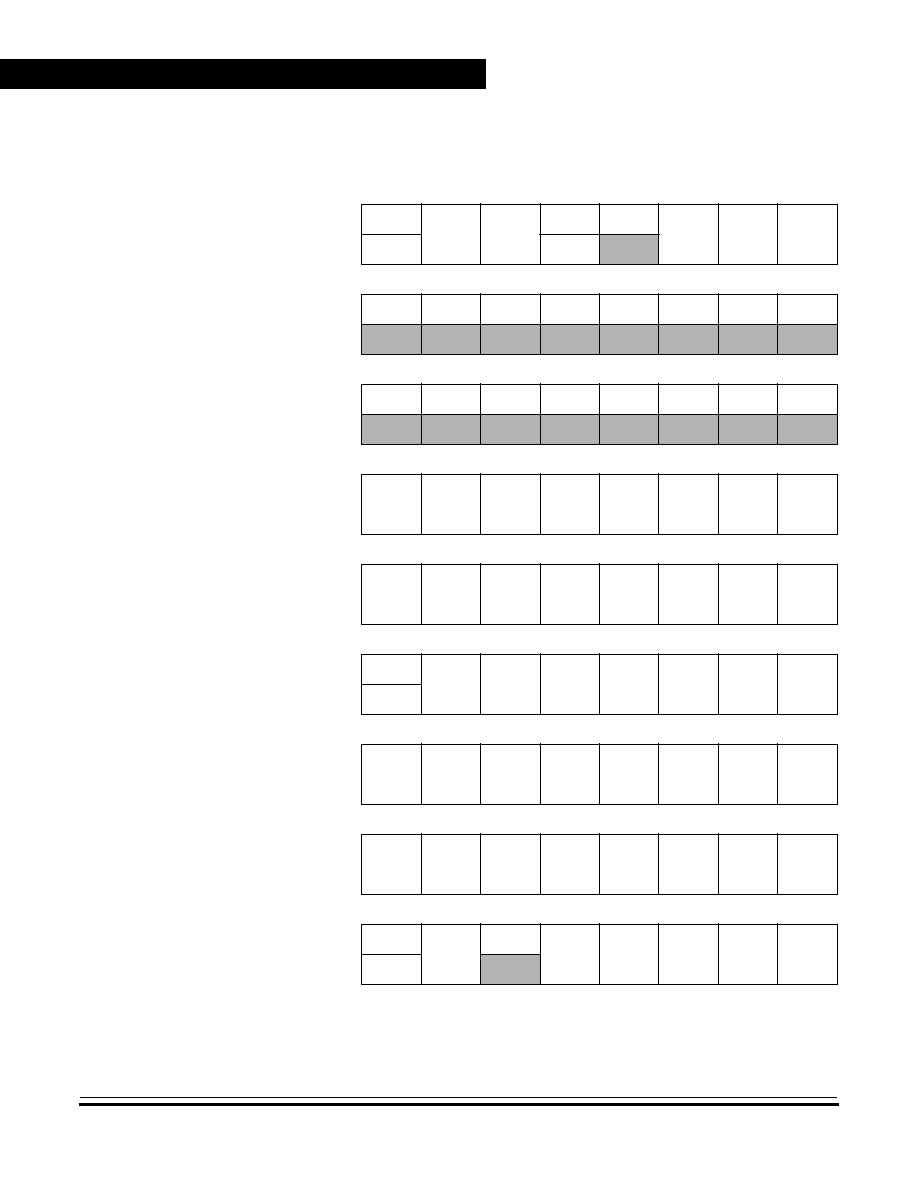
Timer Interface Module (TIM)
Technical Data
MC68H(R)C08JL3
--
Rev. 4
108
Timer Interface Module (TIM)
MOTOROLA
Addr.
Register Name
Bit 7
6
5
4
3
2
1
Bit 0
$0020
TIM Status and Control
Register
(TSC)
Read:
TOF
TOIE
TSTOP
0
0
PS2
PS1
PS0
Write:
0
TRST
Reset:
0
0
1
0
0
0
0
0
$0021
TIM Counter Register High
(TCNTH)
Read:
Bit15
Bit14
Bit13
Bit12
Bit11
Bit10
Bit9
Bit8
Write:
Reset:
0
0
0
0
0
0
0
0
$0022
TIM Counter Register Low
(TCNTL)
Read:
Bit7
Bit6
Bit5
Bit4
Bit3
Bit2
Bit1
Bit0
Write:
Reset:
0
0
0
0
0
0
0
0
$0023
TIM Counter Modulo
Register High
(TMODH)
Read:
Bit15
Bit14
Bit13
Bit12
Bit11
Bit10
Bit9
Bit8
Write:
Reset:
1
1
1
1
1
1
1
1
$0024
TIM Counter Modulo
Register Low
(TMODL)
Read:
Bit7
Bit6
Bit5
Bit4
Bit3
Bit2
Bit1
Bit0
Write:
Reset:
1
1
1
1
1
1
1
1
$0025
TIM Channel 0 Status and
Control Register
(TSC0)
Read:
CH0F
CH0IE
MS0B
MS0A
ELS0B
ELS0A
TOV0
CH0MAX
Write:
0
Reset:
0
0
0
0
0
0
0
0
$0026
TIM Channel 0
Register High
(TCH0H)
Read:
Bit15
Bit14
Bit13
Bit12
Bit11
Bit10
Bit9
Bit8
Write:
Reset:
Indeterminate after reset
$0027
TIM Channel 0
Register Low
(TCH0L)
Read:
Bit7
Bit6
Bit5
Bit4
Bit3
Bit2
Bit1
Bit0
Write:
Reset:
Indeterminate after reset
$0028
TIM Channel 1 Status and
Control Register
(TSC1)
Read:
CH1F
CH1IE
0
MS1A
ELS1B
ELS1A
TOV1
CH1MAX
Write:
0
Reset:
0
0
0
0
0
0
0
0
Figure 10-2. TIM I/O Register Summary

Timer Interface Module (TIM)
Functional Description
MC68H(R)C08JL3
--
Rev. 4
Technical Data
MOTOROLA
Timer Interface Module (TIM)
109
10.5.1 TIM Counter Prescaler
The TIM clock source is one of the seven prescaler outputs. The
prescaler generates seven clock rates from the internal bus clock. The
prescaler select bits, PS[2:0], in the TIM status and control register
(TSC) select the TIM clock source.
10.5.2 Input Capture
With the input capture function, the TIM can capture the time at which an
external event occurs. When an active edge occurs on the pin of an input
capture channel, the TIM latches the contents of the TIM counter into the
TIM channel registers, TCHxH:TCHxL. The polarity of the active edge is
programmable. Input captures can generate TIM CPU interrupt
requests.
10.5.3 Output Compare
With the output compare function, the TIM can generate a periodic pulse
with a programmable polarity, duration, and frequency. When the
counter reaches the value in the registers of an output compare channel,
the TIM can set, clear, or toggle the channel pin. Output compares can
generate TIM CPU interrupt requests.
$0029
TIM Channel 1
Register High
(TCH1H)
Read:
Bit15
Bit14
Bit13
Bit12
Bit11
Bit10
Bit9
Bit8
Write:
Reset:
Indeterminate after reset
$002A
TIM Channel 1
Register Low
(TCH1L)
Read:
Bit7
Bit6
Bit5
Bit4
Bit3
Bit2
Bit1
Bit0
Write:
Reset:
Indeterminate after reset
= Unimplemented
Figure 10-2. TIM I/O Register Summary

Timer Interface Module (TIM)
Technical Data
MC68H(R)C08JL3
--
Rev. 4
110
Timer Interface Module (TIM)
MOTOROLA
10.5.3.1 Unbuffered Output Compare
Any output compare channel can generate unbuffered output compare
pulses as described in
10.5.3 Output Compare
. The pulses are
unbuffered because changing the output compare value requires writing
the new value over the old value currently in the TIM channel registers.
An unsynchronized write to the TIM channel registers to change an
output compare value could cause incorrect operation for up to two
counter overflow periods. For example, writing a new value before the
counter reaches the old value but after the counter reaches the new
value prevents any compare during that counter overflow period. Also,
using a TIM overflow interrupt routine to write a new, smaller output
compare value may cause the compare to be missed. The TIM may pass
the new value before it is written.
Use the following methods to synchronize unbuffered changes in the
output compare value on channel x:
∑
When changing to a smaller value, enable channel x output
compare interrupts and write the new value in the output compare
interrupt routine. The output compare interrupt occurs at the end
of the current output compare pulse. The interrupt routine has until
the end of the counter overflow period to write the new value.
∑
When changing to a larger output compare value, enable
channel x TIM overflow interrupts and write the new value in the
TIM overflow interrupt routine. The TIM overflow interrupt occurs
at the end of the current counter overflow period. Writing a larger
value in an output compare interrupt routine (at the end of the
current pulse) could cause two output compares to occur in the
same counter overflow period.
10.5.3.2 Buffered Output Compare
Channels 0 and 1 can be linked to form a buffered output compare
channel whose output appears on the TCH0 pin. The TIM channel
registers of the linked pair alternately control the output.
Setting the MS0B bit in TIM channel 0 status and control register (TSC0)
links channel 0 and channel 1. The output compare value in the TIM

Timer Interface Module (TIM)
Functional Description
MC68H(R)C08JL3
--
Rev. 4
Technical Data
MOTOROLA
Timer Interface Module (TIM)
111
channel 0 registers initially controls the output on the TCH0 pin. Writing
to the TIM channel 1 registers enables the TIM channel 1 registers to
synchronously control the output after the TIM overflows. At each
subsequent overflow, the TIM channel registers (0 or 1) that control the
output are the ones written to last. TSC0 controls and monitors the
buffered output compare function, and TIM channel 1 status and control
register (TSC1) is unused. While the MS0B bit is set, the channel 1 pin,
TCH1, is available as a general-purpose I/O pin.
NOTE:
In buffered output compare operation, do not write new output compare
values to the currently active channel registers. Writing to the active
channel registers is the same as generating unbuffered output
compares.
10.5.4 Pulse Width Modulation (PWM)
By using the toggle-on-overflow feature with an output compare channel,
the TIM can generate a PWM signal. The value in the TIM counter
modulo registers determines the period of the PWM signal. The channel
pin toggles when the counter reaches the value in the TIM counter
modulo registers. The time between overflows is the period of the PWM
signal.
As
Figure 10-3
shows, the output compare value in the TIM channel
registers determines the pulse width of the PWM signal. The time
between overflow and output compare is the pulse width. Program the
TIM to clear the channel pin on output compare if the state of the PWM
pulse is logic one. Program the TIM to set the pin if the state of the PWM
pulse is logic zero.

Timer Interface Module (TIM)
Technical Data
MC68H(R)C08JL3
--
Rev. 4
112
Timer Interface Module (TIM)
MOTOROLA
Figure 10-3. PWM Period and Pulse Width
The value in the TIM counter modulo registers and the selected
prescaler output determines the frequency of the PWM output. The
frequency of an 8-bit PWM signal is variable in 256 increments. Writing
$00FF (255) to the TIM counter modulo registers produces a PWM
period of 256 times the internal bus clock period if the prescaler select
value is 000
(see 10.10.1 TIM Status and Control Register (TSC)
).
The value in the TIM channel registers determines the pulse width of the
PWM output. The pulse width of an 8-bit PWM signal is variable in 256
increments. Writing $0080 (128) to the TIM channel registers produces
a duty cycle of 128/256 or 50%.
10.5.4.1 Unbuffered PWM Signal Generation
Any output compare channel can generate unbuffered PWM pulses as
described in
10.5.4 Pulse Width Modulation (PWM)
. The pulses are
unbuffered because changing the pulse width requires writing the new
pulse width value over the old value currently in the TIM channel
registers.
An unsynchronized write to the TIM channel registers to change a pulse
width value could cause incorrect operation for up to two PWM periods.
For example, writing a new value before the counter reaches the old
value but after the counter reaches the new value prevents any compare
during that PWM period. Also, using a TIM overflow interrupt routine to
TCHx
PERIOD
PULSE
WIDTH
OVERFLOW
OVERFLOW
OVERFLOW
OUTPUT
COMPARE
OUTPUT
COMPARE
OUTPUT
COMPARE

Timer Interface Module (TIM)
Functional Description
MC68H(R)C08JL3
--
Rev. 4
Technical Data
MOTOROLA
Timer Interface Module (TIM)
113
write a new, smaller pulse width value may cause the compare to be
missed. The TIM may pass the new value before it is written.
Use the following methods to synchronize unbuffered changes in the
PWM pulse width on channel x:
∑
When changing to a shorter pulse width, enable channel x output
compare interrupts and write the new value in the output compare
interrupt routine. The output compare interrupt occurs at the end
of the current pulse. The interrupt routine has until the end of the
PWM period to write the new value.
∑
When changing to a longer pulse width, enable channel x TIM
overflow interrupts and write the new value in the TIM overflow
interrupt routine. The TIM overflow interrupt occurs at the end of
the current PWM period. Writing a larger value in an output
compare interrupt routine (at the end of the current pulse) could
cause two output compares to occur in the same PWM period.
NOTE:
In PWM signal generation, do not program the PWM channel to toggle
on output compare. Toggling on output compare prevents reliable 0%
duty cycle generation and removes the ability of the channel to self-
correct in the event of software error or noise. Toggling on output
compare also can cause incorrect PWM signal generation when
changing the PWM pulse width to a new, much larger value.
10.5.4.2 Buffered PWM Signal Generation
Channels 0 and 1 can be linked to form a buffered PWM channel whose
output appears on the TCH0 pin. The TIM channel registers of the linked
pair alternately control the pulse width of the output.
Setting the MS0B bit in TIM channel 0 status and control register (TSC0)
links channel 0 and channel 1. The TIM channel 0 registers initially
control the pulse width on the TCH0 pin. Writing to the TIM channel 1
registers enables the TIM channel 1 registers to synchronously control
the pulse width at the beginning of the next PWM period. At each
subsequent overflow, the TIM channel registers (0 or 1) that control the
pulse width are the ones written to last. TSC0 controls and monitors the
buffered PWM function, and TIM channel 1 status and control register

Timer Interface Module (TIM)
Technical Data
MC68H(R)C08JL3
--
Rev. 4
114
Timer Interface Module (TIM)
MOTOROLA
(TSC1) is unused. While the MS0B bit is set, the channel 1 pin, TCH1,
is available as a general-purpose I/O pin.
NOTE:
In buffered PWM signal generation, do not write new pulse width values
to the currently active channel registers. Writing to the active channel
registers is the same as generating unbuffered PWM signals.
10.5.4.3 PWM Initialization
To ensure correct operation when generating unbuffered or buffered
PWM signals, use the following initialization procedure:
1. In the TIM status and control register (TSC):
a.
Stop the TIM counter by setting the TIM stop bit, TSTOP.
b.
Reset the TIM counter by setting the TIM reset bit, TRST.
2. In the TIM counter modulo registers (TMODH:TMODL), write the
value for the required PWM period.
3. In the TIM channel x registers (TCHxH:TCHxL), write the value for
the required pulse width.
4. In TIM channel x status and control register (TSCx):
a.
Write 0:1 (for unbuffered output compare or PWM signals) or
1:0 (for buffered output compare or PWM signals) to the mode
select bits, MSxB:MSxA.
(See Table 10-3
.)
b.
Write 1 to the toggle-on-overflow bit, TOVx.
c.
Write 1:0 (to clear output on compare) or 1:1 (to set output on
compare) to the edge/level select bits, ELSxB:ELSxA. The
output action on compare must force the output to the
complement of the pulse width level. (See
Table 10-3
.)
NOTE:
In PWM signal generation, do not program the PWM channel to toggle
on output compare. Toggling on output compare prevents reliable 0%
duty cycle generation and removes the ability of the channel to self-
correct in the event of software error or noise. Toggling on output
compare can also cause incorrect PWM signal generation when
changing the PWM pulse width to a new, much larger value.
5. In the TIM status control register (TSC), clear the TIM stop bit,
TSTOP.

Timer Interface Module (TIM)
Interrupts
MC68H(R)C08JL3
--
Rev. 4
Technical Data
MOTOROLA
Timer Interface Module (TIM)
115
Setting MS0B links channels 0 and 1 and configures them for buffered
PWM operation. The TIM channel 0 registers (TCH0H:TCH0L) initially
control the buffered PWM output. TIM status control register 0 (TSCR0)
controls and monitors the PWM signal from the linked channels. MS0B
takes priority over MS0A.
Clearing the toggle-on-overflow bit, TOVx, inhibits output toggles on TIM
overflows. Subsequent output compares try to force the output to a state
it is already in and have no effect. The result is a 0% duty cycle output.
Setting the channel x maximum duty cycle bit (CHxMAX) and clearing
the TOVx bit generates a 100% duty cycle output. (See
10.10.4 TIM
Channel Status and Control Registers (TSC0:TSC1)
.)
10.6 Interrupts
The following TIM sources can generate interrupt requests:
∑
TIM overflow flag (TOF) -- The TOF bit is set when the TIM
counter value rolls over to $0000 after matching the value in the
TIM counter modulo registers. The TIM overflow interrupt enable
bit, TOIE, enables TIM overflow CPU interrupt requests. TOF and
TOIE are in the TIM status and control register.
∑
TIM channel flags (CH1F:CH0F) -- The CHxF bit is set when an
input capture or output compare occurs on channel x. Channel x
TIM CPU interrupt requests are controlled by the channel x
interrupt enable bit, CHxIE. Channel x TIM CPU interrupt requests
are enabled when CHxIE=1. CHxF and CHxIE are in the TIM
channel x status and control register.
10.7 Wait Mode
The WAIT instruction puts the MCU in low-power-consumption standby
mode.
The TIM remains active after the execution of a WAIT instruction. In wait
mode the TIM registers are not accessible by the CPU. Any enabled
CPU interrupt request from the TIM can bring the MCU out of wait mode.

Timer Interface Module (TIM)
Technical Data
MC68H(R)C08JL3
--
Rev. 4
116
Timer Interface Module (TIM)
MOTOROLA
If TIM functions are not required during wait mode, reduce power
consumption by stopping the TIM before executing the WAIT instruction.
10.8 TIM During Break Interrupts
A break interrupt stops the TIM counter.
The system integration module (SIM) controls whether status bits in
other modules can be cleared during the break state. The BCFE bit in
the break flag control register (BFCR) enables software to clear status
bits during the break state.
(See 7.8.3 Break Flag Control Register
(BFCR)
.)
To allow software to clear status bits during a break interrupt, write a
logic one to the BCFE bit. If a status bit is cleared during the break state,
it remains cleared when the MCU exits the break state.
To protect status bits during the break state, write a logic zero to the
BCFE bit. With BCFE at logic zero (its default state), software can read
and write I/O registers during the break state without affecting status
bits. Some status bits have a two-step read/write clearing procedure. If
software does the first step on such a bit before the break, the bit cannot
change during the break state as long as BCFE is at logic zero. After the
break, doing the second step clears the status bit.
10.9 I/O Signals
Port D shares two of its pins with the TIM. The two TIM channel I/O pins
are PTD4/TCH0 and PTD5/TCH1.
Each channel I/O pin is programmable independently as an input
capture pin or an output compare pin. PTD4/TCH0 can be configured as
a buffered output compare or buffered PWM pin.

Timer Interface Module (TIM)
I/O Registers
MC68H(R)C08JL3
--
Rev. 4
Technical Data
MOTOROLA
Timer Interface Module (TIM)
117
10.10 I/O Registers
The following I/O registers control and monitor operation of the TIM:
∑
TIM status and control register (TSC)
∑
TIM control registers (TCNTH:TCNTL)
∑
TIM counter modulo registers (TMODH:TMODL)
∑
TIM channel status and control registers (TSC0 and TSC1)
∑
TIM channel registers (TCH0H:TCH0L and TCH1H:TCH1L)
10.10.1 TIM Status and Control Register (TSC)
The TIM status and control register does the following:
∑
Enables TIM overflow interrupts
∑
Flags TIM overflows
∑
Stops the TIM counter
∑
Resets the TIM counter
∑
Prescales the TIM counter clock
TOF -- TIM Overflow Flag Bit
This read/write flag is set when the TIM counter resets to $0000 after
reaching the modulo value programmed in the TIM counter modulo
registers. Clear TOF by reading the TIM status and control register
when TOF is set and then writing a logic zero to TOF. If another TIM
Address:
$0020
Bit 7
6
5
4
3
2
1
Bit 0
Read:
TOF
TOIE
TSTOP
0
0
PS2
PS1
PS0
Write:
0
TRST
Reset:
0
0
1
0
0
0
0
0
= Unimplemented
Figure 10-4. TIM Status and Control Register (TSC)

Timer Interface Module (TIM)
Technical Data
MC68H(R)C08JL3
--
Rev. 4
118
Timer Interface Module (TIM)
MOTOROLA
overflow occurs before the clearing sequence is complete, then
writing logic zero to TOF has no effect. Therefore, a TOF interrupt
request cannot be lost due to inadvertent clearing of TOF. Reset
clears the TOF bit. Writing a logic one to TOF has no effect.
1 = TIM counter has reached modulo value
0 = TIM counter has not reached modulo value
TOIE -- TIM Overflow Interrupt Enable Bit
This read/write bit enables TIM overflow interrupts when the TOF bit
becomes set. Reset clears the TOIE bit.
1 = TIM overflow interrupts enabled
0 = TIM overflow interrupts disabled
TSTOP -- TIM Stop Bit
This read/write bit stops the TIM counter. Counting resumes when
TSTOP is cleared. Reset sets the TSTOP bit, stopping the TIM
counter until software clears the TSTOP bit.
1 = TIM counter stopped
0 = TIM counter active
NOTE:
Do not set the TSTOP bit before entering wait mode if the TIM is required
to exit wait mode.
TRST -- TIM Reset Bit
Setting this write-only bit resets the TIM counter and the TIM
prescaler. Setting TRST has no effect on any other registers.
Counting resumes from $0000. TRST is cleared automatically after
the TIM counter is reset and always reads as logic zero. Reset clears
the TRST bit.
1 = Prescaler and TIM counter cleared
0 = No effect
NOTE:
Setting the TSTOP and TRST bits simultaneously stops the TIM counter
at a value of $0000.
PS[2:0] -- Prescaler Select Bits
These read/write bits select one of the seven prescaler outputs as the
input to the TIM counter as
Table 10-2
shows. Reset clears the
PS[2:0] bits.
Timer Interface Module (TIM)
I/O Registers
MC68H(R)C08JL3
--
Rev. 4
Technical Data
MOTOROLA
Timer Interface Module (TIM)
119
10.10.2 TIM Counter Registers (TCNTH:TCNTL)
The two read-only TIM counter registers contain the high and low bytes
of the value in the TIM counter. Reading the high byte (TCNTH) latches
the contents of the low byte (TCNTL) into a buffer. Subsequent reads of
TCNTH do not affect the latched TCNTL value until TCNTL is read.
Reset clears the TIM counter registers. Setting the TIM reset bit (TRST)
also clears the TIM counter registers.
NOTE:
If you read TCNTH during a break interrupt, be sure to unlatch TCNTL
by reading TCNTL before exiting the break interrupt. Otherwise, TCNTL
retains the value latched during the break.
Table 10-2. Prescaler Selection
PS2
PS1
PS0
TIM Clock Source
0
0
0
Internal Bus Clock ˜ 1
0
0
1
Internal Bus Clock ˜ 2
0
1
0
Internal Bus Clock ˜ 4
0
1
1
Internal Bus Clock ˜ 8
1
0
0
Internal Bus Clock ˜ 16
1
0
1
Internal Bus Clock ˜ 32
1
1
0
Internal Bus Clock ˜ 64
1
1
1
Not available
Timer Interface Module (TIM)
Technical Data
MC68H(R)C08JL3
--
Rev. 4
120
Timer Interface Module (TIM)
MOTOROLA
10.10.3 TIM Counter Modulo Registers (TMODH:TMODL)
The read/write TIM modulo registers contain the modulo value for the
TIM counter. When the TIM counter reaches the modulo value, the
overflow flag (TOF) becomes set, and the TIM counter resumes counting
from $0000 at the next clock. Writing to the high byte (TMODH) inhibits
the TOF bit and overflow interrupts until the low byte (TMODL) is written.
Reset sets the TIM counter modulo registers.
Address:
$0021
TCNTH
Bit 7
6
5
4
3
2
1
Bit 0
Read:
Bit15
Bit14
Bit13
Bit12
Bit11
Bit10
Bit9
Bit8
Write:
Reset:
0
0
0
0
0
0
0
0
Address:
$0022
TCNTL
Bit 7
6
5
4
3
2
1
Bit 0
Read:
Bit7
Bit6
Bit5
Bit4
Bit3
Bit2
Bit1
Bit0
Write:
Reset:
0
0
0
0
0
0
0
0
= Unimplemented
Figure 10-5. TIM Counter Registers (TCNTH:TCNTL)

Timer Interface Module (TIM)
I/O Registers
MC68H(R)C08JL3
--
Rev. 4
Technical Data
MOTOROLA
Timer Interface Module (TIM)
121
NOTE:
Reset the TIM counter before writing to the TIM counter modulo registers.
10.10.4 TIM Channel Status and Control Registers (TSC0:TSC1)
Each of the TIM channel status and control registers does the following:
∑
Flags input captures and output compares
∑
Enables input capture and output compare interrupts
∑
Selects input capture, output compare, or PWM operation
∑
Selects high, low, or toggling output on output compare
∑
Selects rising edge, falling edge, or any edge as the active input
capture trigger
∑
Selects output toggling on TIM overflow
∑
Selects 100% PWM duty cycle
∑
Selects buffered or unbuffered output compare/PWM operation
Address:
$0023
TMODH
Bit 7
6
5
4
3
2
1
Bit 0
Read:
Bit15
Bit14
Bit13
Bit12
Bit11
Bit10
Bit9
Bit8
Write:
Reset:
1
1
1
1
1
1
1
1
Address:
$0024
TMODL
Bit 7
6
5
4
3
2
1
Bit 0
Read:
Bit7
Bit6
Bit5
Bit4
Bit3
Bit2
Bit1
Bit0
Write:
Reset:
1
1
1
1
1
1
1
1
Figure 10-6. TIM Counter Modulo Registers (TMODH:TMODL)

Timer Interface Module (TIM)
Technical Data
MC68H(R)C08JL3
--
Rev. 4
122
Timer Interface Module (TIM)
MOTOROLA
CHxF -- Channel x Flag Bit
When channel x is an input capture channel, this read/write bit is set
when an active edge occurs on the channel x pin. When channel x is
an output compare channel, CHxF is set when the value in the TIM
counter registers matches the value in the TIM channel x registers.
When TIM CPU interrupt requests are enabled (CHxIE=1), clear
CHxF by reading the TIM channel x status and control register with
CHxF set and then writing a logic zero to CHxF. If another interrupt
request occurs before the clearing sequence is complete, then writing
logic zero to CHxF has no effect. Therefore, an interrupt request
cannot be lost due to inadvertent clearing of CHxF.
Reset clears the CHxF bit. Writing a logic one to CHxF has no effect.
1 = Input capture or output compare on channel x
0 = No input capture or output compare on channel x
CHxIE -- Channel x Interrupt Enable Bit
This read/write bit enables TIM CPU interrupt service requests on
channel x. Reset clears the CHxIE bit.
1 = Channel x CPU interrupt requests enabled
0 = Channel x CPU interrupt requests disabled
Address:
$0025
TSC0
Bit 7
6
5
4
3
2
1
Bit 0
Read:
CH0F
CH0IE
MS0B
MS0A
ELS0B
ELS0A
TOV0
CH0MAX
Write:
0
Reset:
0
0
0
0
0
0
0
0
Address:
$0028
TSC1
Bit 7
6
5
4
3
2
1
Bit 0
Read:
CH1F
CH1IE
0
MS1A
ELS1B
ELS1A
TOV1
CH1MAX
Write:
0
Reset:
0
0
0
0
0
0
0
0
= Unimplemented
Figure 10-7. TIM Channel Status and Control Registers (TSC0:TSC1)

Timer Interface Module (TIM)
I/O Registers
MC68H(R)C08JL3
--
Rev. 4
Technical Data
MOTOROLA
Timer Interface Module (TIM)
123
MSxB -- Mode Select Bit B
This read/write bit selects buffered output compare/PWM operation.
MSxB exists only in the TIM channel 0 status and control register.
Setting MS0B disables the channel 1 status and control register and
reverts TCH1 to general-purpose I/O.
Reset clears the MSxB bit.
1 = Buffered output compare/PWM operation enabled
0 = Buffered output compare/PWM operation disabled
MSxA -- Mode Select Bit A
When ELSxB:A
00, this read/write bit selects either input capture
operation or unbuffered output compare/PWM operation.
See
Table 10-3
.
1 = Unbuffered output compare/PWM operation
0 = Input capture operation
When ELSxB:A = 00, this read/write bit selects the initial output level
of the TCHx pin. (See
Table 10-3
.) Reset clears the MSxA bit.
1 = Initial output level low
0 = Initial output level high
NOTE:
Before changing a channel function by writing to the MSxB or MSxA bit,
set the TSTOP and TRST bits in the TIM status and control register
(TSC).
ELSxB and ELSxA -- Edge/Level Select Bits
When channel x is an input capture channel, these read/write bits
control the active edge-sensing logic on channel x.
When channel x is an output compare channel, ELSxB and ELSxA
control the channel x output behavior when an output compare
occurs.
When ELSxB and ELSxA are both clear, channel x is not connected
to an I/O port, and pin TCHx is available as a general-purpose I/O
pin.
Table 10-3
shows how ELSxB and ELSxA work. Reset clears the
ELSxB and ELSxA bits.
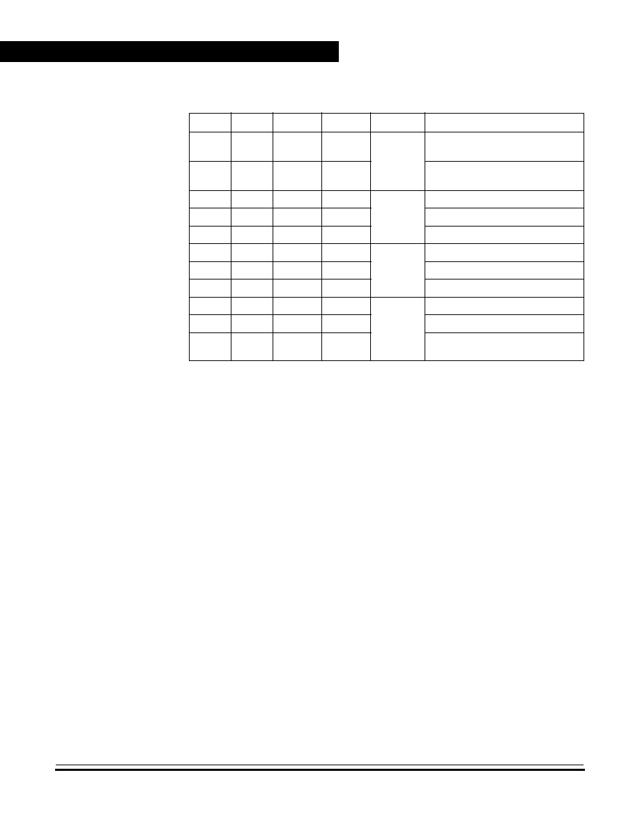
Timer Interface Module (TIM)
Technical Data
MC68H(R)C08JL3
--
Rev. 4
124
Timer Interface Module (TIM)
MOTOROLA
NOTE:
Before enabling a TIM channel register for input capture operation, make
sure that the TCHx pin is stable for at least two bus clocks.
TOVx -- Toggle-On-Overflow Bit
When channel x is an output compare channel, this read/write bit
controls the behavior of the channel x output when the TIM counter
overflows. When channel x is an input capture channel, TOVx has no
effect. Reset clears the TOVx bit.
1 = Channel x pin toggles on TIM counter overflow.
0 = Channel x pin does not toggle on TIM counter overflow.
NOTE:
When TOVx is set, a TIM counter overflow takes precedence over a
channel x output compare if both occur at the same time.
CHxMAX -- Channel x Maximum Duty Cycle Bit
When the TOVx bit is at logic zero, setting the CHxMAX bit forces the
duty cycle of buffered and unbuffered PWM signals to 100%. As
Figure 10-8
shows, the CHxMAX bit takes effect in the cycle after it
is set or cleared. The output stays at the 100% duty cycle level until
the cycle after CHxMAX is cleared.
Table 10-3. Mode, Edge, and Level Selection
MSxB
MSxA
ELSxB
ELSxA
Mode
Configuration
X
0
0
0
Output
Preset
Pin under Port Control;
Initial Output Level High
X
1
0
0
Pin under Port Control;
Initial Output Level Low
0
0
0
1
Input
Capture
Capture on Rising Edge Only
0
0
1
0
Capture on Falling Edge Only
0
0
1
1
Capture on Rising or Falling Edge
0
1
0
1
Output
Compare
or PWM
Toggle Output on Compare
0
1
1
0
Clear Output on Compare
0
1
1
1
Set Output on Compare
1
X
0
1
Buffered
Output
Compare or
Buffered
PWM
Toggle Output on Compare
1
X
1
0
Clear Output on Compare
1
X
1
1
Set Output on Compare
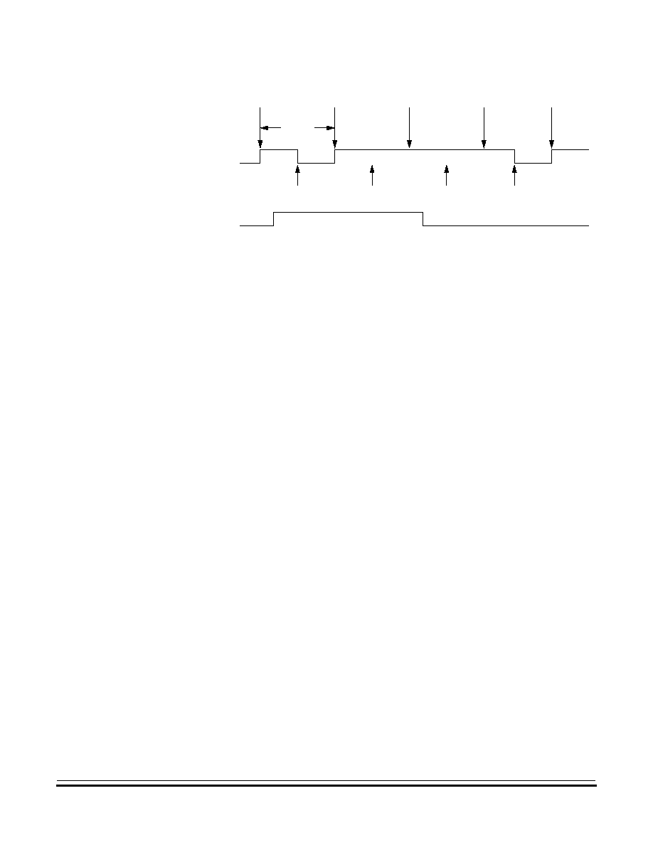
Timer Interface Module (TIM)
I/O Registers
MC68H(R)C08JL3
--
Rev. 4
Technical Data
MOTOROLA
Timer Interface Module (TIM)
125
Figure 10-8. CHxMAX Latency
10.10.5 TIM Channel Registers (TCH0H/L:TCH1H/L)
These read/write registers contain the captured TIM counter value of the
input capture function or the output compare value of the output
compare function. The state of the TIM channel registers after reset is
unknown.
In input capture mode (MSxB:MSxA = 0:0), reading the high byte of the
TIM channel x registers (TCHxH) inhibits input captures until the low
byte (TCHxL) is read.
In output compare mode (MSxB:MSxA
0:0), writing to the high byte of
the TIM channel x registers (TCHxH) inhibits output compares until the
low byte (TCHxL) is written.
OUTPUT
OVERFLOW
TCHx
PERIOD
CHxMAX
OVERFLOW
OVERFLOW
OVERFLOW
OVERFLOW
COMPARE
OUTPUT
COMPARE
OUTPUT
COMPARE
OUTPUT
COMPARE

Timer Interface Module (TIM)
Technical Data
MC68H(R)C08JL3
--
Rev. 4
126
Timer Interface Module (TIM)
MOTOROLA
Address:
$0026
TCH0H
Bit 7
6
5
4
3
2
1
Bit 0
Read:
Bit15
Bit14
Bit13
Bit12
Bit11
Bit10
Bit9
Bit8
Write:
Reset:
Indeterminate after reset
Address:
$0027
TCH0L
Bit 7
6
5
4
3
2
1
Bit 0
Read:
Bit7
Bit6
Bit5
Bit4
Bit3
Bit2
Bit1
Bit0
Write:
Reset:
Indeterminate after reset
Address:
$0029
TCH1H
Bit 7
6
5
4
3
2
1
Bit 0
Read:
Bit15
Bit14
Bit13
Bit12
Bit11
Bit10
Bit9
Bit8
Write:
Reset:
Indeterminate after reset
Address:
$02A
TCH1L
Bit 7
6
5
4
3
2
1
Bit 0
Read:
Bit7
Bit6
Bit5
Bit4
Bit3
Bit2
Bit1
Bit0
Write:
Reset:
Indeterminate after reset
Figure 10-9. TIM Channel Registers (TCH0H/L:TCH1H/L)

MC68H(R)C08JL3
--
Rev. 4
Technical Data
MOTOROLA
Analog-to-Digital Converter (ADC)
127
Technical Data -- MC68H(R)C08JL3
Section 11. Analog-to-Digital Converter (ADC)
11.1 Contents
11.2
Introduction . . . . . . . . . . . . . . . . . . . . . . . . . . . . . . . . . . . . . . . 127
11.3
Features . . . . . . . . . . . . . . . . . . . . . . . . . . . . . . . . . . . . . . . . . 128
11.4
Functional Description . . . . . . . . . . . . . . . . . . . . . . . . . . . . . . 128
11.4.1
ADC Port I/O Pins . . . . . . . . . . . . . . . . . . . . . . . . . . . . . . . 129
11.4.2
Voltage Conversion . . . . . . . . . . . . . . . . . . . . . . . . . . . . . . 130
11.4.3
Conversion Time . . . . . . . . . . . . . . . . . . . . . . . . . . . . . . . . 130
11.4.4
Continuous Conversion . . . . . . . . . . . . . . . . . . . . . . . . . . . 130
11.4.5
Accuracy and Precision . . . . . . . . . . . . . . . . . . . . . . . . . . . 131
11.5
Interrupts. . . . . . . . . . . . . . . . . . . . . . . . . . . . . . . . . . . . . . . . . 131
11.6
Low-Power Modes . . . . . . . . . . . . . . . . . . . . . . . . . . . . . . . . . 131
11.6.1
Wait Mode . . . . . . . . . . . . . . . . . . . . . . . . . . . . . . . . . . . . . 131
11.6.2
Stop Mode . . . . . . . . . . . . . . . . . . . . . . . . . . . . . . . . . . . . . 131
11.7
I/O Signals . . . . . . . . . . . . . . . . . . . . . . . . . . . . . . . . . . . . . . . 131
11.7.1
ADC Voltage In (ADCVIN) . . . . . . . . . . . . . . . . . . . . . . . . . 132
11.8
I/O Registers. . . . . . . . . . . . . . . . . . . . . . . . . . . . . . . . . . . . . . 132
11.8.1
ADC Status and Control Register. . . . . . . . . . . . . . . . . . . . 132
11.8.2
ADC Data Register. . . . . . . . . . . . . . . . . . . . . . . . . . . . . . . 134
11.8.3
ADC Input Clock Register . . . . . . . . . . . . . . . . . . . . . . . . . 135
11.2 Introduction
This section describes the analog-to-digital converter (ADC). The ADC
is an 8-bit, 12-channels analog-to-digital converter.

Analog-to-Digital Converter (ADC)
Technical Data
MC68H(R)C08JL3
--
Rev. 4
128
Analog-to-Digital Converter (ADC)
MOTOROLA
11.3 Features
Features of the ADC module include:
∑
12 channels with multiplexed input
∑
Linear successive approximation with monotonicity
∑
8-bit resolution
∑
Single or continuous conversion
∑
Conversion complete flag or conversion complete interrupt
∑
Selectable ADC clock
11.4 Functional Description
Twelve ADC channels are available for sampling external sources at
pins PTB0≠PTB7 and PTD0≠PTD3. An analog multiplexer allows the
single ADC converter to select one of the 12 ADC channels as ADC
voltage input (ADCVIN). ADCVIN is converted by the successive
approximation register-based counters. The ADC resolution is 8 bits.
When the conversion is completed, ADC puts the result in the ADC data
register and sets a flag or generates an interrupt.
Figure 11-2
shows a
block diagram of the ADC.
Addr.
Register Name
Bit 7
6
5
4
3
2
1
Bit 0
$003C
ADC Status and Control
Register
(ADSCR)
Read:
COCO
AIEN
ADCO
CH4
CH3
CH2
CH1
CH0
Write:
Reset:
0
0
0
1
1
1
1
1
$003D
ADC Data Register
(ADR)
Read:
AD7
AD6
AD5
AD4
AD3
AD2
AD1
AD0
Write:
Reset:
Indeterminate after reset
$003E
ADC Input Clock Register
(ADICLK)
Read:
ADIV2
ADIV1
ADIV0
0
0
0
0
0
Write:
Reset:
0
0
0
0
0
0
0
0
Figure 11-1. ADC I/O Register Summary

Analog-to-Digital Converter (ADC)
Functional Description
MC68H(R)C08JL3
--
Rev. 4
Technical Data
MOTOROLA
Analog-to-Digital Converter (ADC)
129
Figure 11-2. ADC Block Diagram
11.4.1 ADC Port I/O Pins
PTB0≠PTB7 and PTD0≠PTD3 are general-purpose I/O pins that are
shared with the ADC channels. The channel select bits (ADC Status and
Control register, $003C), define which ADC channel/port pin will be used
as the input signal. The ADC overrides the port I/O logic by forcing that
pin as input to the ADC. The remaining ADC channels/port pins are
controlled by the port I/O logic and can be used as general-purpose I/O.
INTERNAL
DATA BUS
INTERRUPT
LOGIC
CHANNEL
SELECT
ADC
CLOCK
GENERATOR
CONVERSION
COMPLETE
ADC VOLTAGE IN
ADCVIN
ADC CLOCK
BUS CLOCK
CH[4:0]
ADC DATA REGISTER
ADIV[2:0]
ADICLK
AIEN
COCO
DISABLE
DISABLE
ADC CHANNEL x
READ DDRB/DDRD
WRITE DDRB/DDRD
RESET
WRITE PTB/PTD
READ PTB/PTD
DDRBx/DDRDx
PTBx/PTDx
(1 OF 12 CHANNELS)
ADCx

Analog-to-Digital Converter (ADC)
Technical Data
MC68H(R)C08JL3
--
Rev. 4
130
Analog-to-Digital Converter (ADC)
MOTOROLA
Writes to the port register or DDR will not have any affect on the port pin
that is selected by the ADC. Read of a port pin which is in use by the
ADC will return a logic 0 if the corresponding DDR bit is at logic 0. If the
DDR bit is at logic 1, the value in the port data latch is read.
11.4.2 Voltage Conversion
When the input voltage to the ADC equals V
DD
, the ADC converts the
signal to $FF (full scale). If the input voltage equals V
SS,
the ADC
converts it to $00. Input voltages between V
DD
and V
SS
are a
straight-line linear conversion. All other input voltages will result in $FF
if greater than V
DD
and $00 if less than V
SS
.
NOTE:
Input voltage should not exceed the analog supply voltages.
11.4.3 Conversion Time
Sixteen ADC internal clocks are required to perform one conversion. The
ADC starts a conversion on the first rising edge of the ADC internal clock
immediately following a write to the ADSCR. If the ADC internal clock is
selected to run at 1MHz, then one conversion will take 16
µ
s to complete.
With a 1MHz ADC internal clock the maximum sample rate is 62.5kHz.
11.4.4 Continuous Conversion
In the continuous conversion mode, the ADC continuously converts the
selected channel filling the ADC data register with new data after each
conversion. Data from the previous conversion will be overwritten
whether that data has been read or not. Conversions will continue until
the ADCO bit is cleared. The COCO bit (ADC Status & Control register,
$003C) is set after each conversion and can be cleared by writing the
ADC status and control register or reading of the ADC data register.
16 ADC Clock Cycles
Conversion Time =
ADC Clock Frequency
Number of Bus Cycles = Conversion Time
◊
Bus Frequency

Analog-to-Digital Converter (ADC)
Interrupts
MC68H(R)C08JL3
--
Rev. 4
Technical Data
MOTOROLA
Analog-to-Digital Converter (ADC)
131
11.4.5 Accuracy and Precision
The conversion process is monotonic and has no missing codes.
11.5 Interrupts
When the AIEN bit is set, the ADC module is capable of generating a
CPU interrupt after each ADC conversion. A CPU interrupt is generated
if the COCO bit is at logic 0. The COCO bit is not used as a conversion
complete flag when interrupts are enabled.
11.6 Low-Power Modes
The following subsections describe the ADC in low-power modes.
11.6.1 Wait Mode
The ADC continues normal operation during wait mode. Any enabled
CPU interrupt request from the ADC can bring the MCU out of wait
mode. If the ADC is not required to bring the MCU out of wait mode,
power down the ADC by setting the CH[4:0] bits in the ADC Status and
Control register to logic 1's before executing the WAIT instruction.
11.6.2 Stop Mode
The ADC module is inactive after the execution of a STOP instruction.
Any pending conversion is aborted. ADC conversions resume when the
MCU exits stop mode. Allow one conversion cycle to stabilize the analog
circuitry before attempting a new ADC conversion after exiting stop
mode.
11.7 I/O Signals
The ADC module has 12 channels that are shared with I/O port B and
port D.

Analog-to-Digital Converter (ADC)
Technical Data
MC68H(R)C08JL3
--
Rev. 4
132
Analog-to-Digital Converter (ADC)
MOTOROLA
11.7.1 ADC Voltage In (ADCVIN)
ADCVIN is the input voltage signal from one of the 12 ADC channels to
the ADC module.
11.8 I/O Registers
These I/O registers control and monitor ADC operation:
∑
ADC Status and Control register (ADSCR)
∑
ADC data register (ADR)
∑
ADC clock register (ADICLK)
11.8.1 ADC Status and Control Register
The following paragraphs describe the function of the ADC Status and
Control register.
COCO -- Conversions Complete Bit
When the AIEN bit is a logic 0, the COCO is a read-only bit which is
set each time a conversion is completed. This bit is cleared whenever
the ADC status and control register is written or whenever the ADC
data register is read. Reset clears this bit.
1 = conversion completed (AIEN = 0)
0 = conversion not completed (AIEN = 0)
When the AIEN bit is a logic 1 (CPU interrupt enabled), the COCO is
a read-only bit, and will always be logic 0 when read.
Address:
$003C
Bit 7
6
5
4
3
2
1
Bit 0
Read:
COCO
AIEN
ADCO
CH4
CH3
CH2
CH1
CH0
Write:
Reset:
0
0
0
1
1
1
1
1
= Unimplemented
Figure 11-3. ADC Status and Control Register (ADSCR)

Analog-to-Digital Converter (ADC)
I/O Registers
MC68H(R)C08JL3
--
Rev. 4
Technical Data
MOTOROLA
Analog-to-Digital Converter (ADC)
133
AIEN -- ADC Interrupt Enable Bit
When this bit is set, an interrupt is generated at the end of an ADC
conversion. The interrupt signal is cleared when the data register is
read or the status/control register is written. Reset clears the AIEN bit.
1 = ADC interrupt enabled
0 = ADC interrupt disabled
ADCO -- ADC Continuous Conversion Bit
When set, the ADC will convert samples continuously and update the
ADR register at the end of each conversion. Only one conversion is
allowed when this bit is cleared. Reset clears the ADCO bit.
1 = Continuous ADC conversion
0 = One ADC conversion
ADCH[4:0] -- ADC Channel Select Bits
ADCH4, ADCH3, ADCH2, ADCH1, and ADCH0 form a 5-bit field
which is used to select one of the ADC channels. The five channel
select bits are detailed in the following table. Care should be taken
when using a port pin as both an analog and a digital input
simultaneously to prevent switching noise from corrupting the analog
signal. (See
Table 11-1.)
The ADC subsystem is turned off when the channel select bits are all
set to one. This feature allows for reduced power consumption for the
MCU when the ADC is not used. Reset sets all of these bits to a
logic 1.
NOTE:
Recovery from the disabled state requires one conversion cycle to
stabilize.
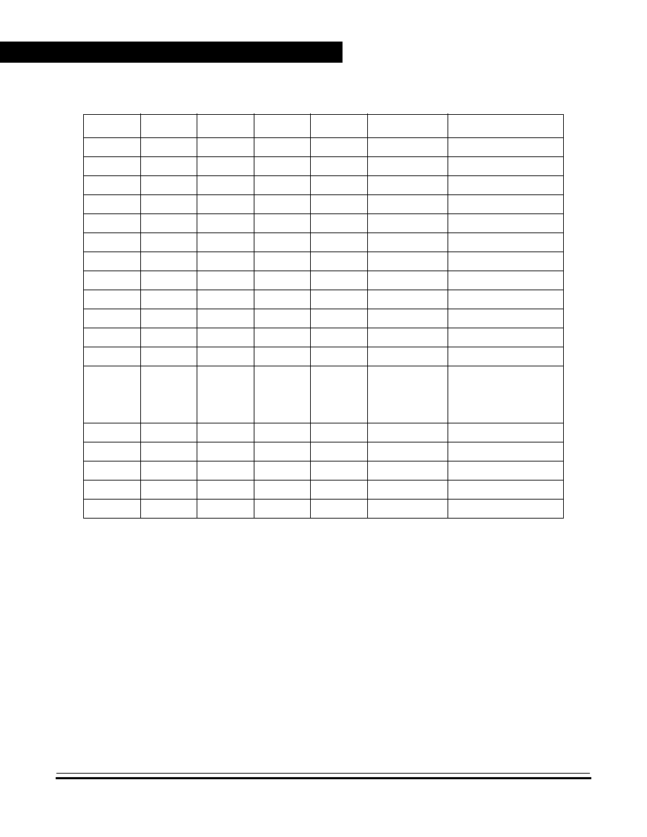
Analog-to-Digital Converter (ADC)
Technical Data
MC68H(R)C08JL3
--
Rev. 4
134
Analog-to-Digital Converter (ADC)
MOTOROLA
11.8.2 ADC Data Register
One 8-bit result register is provided. This register is updated each time
an ADC conversion completes.
Table 11-1. MUX Channel Select
CH4
CH3
CH2
CH1
CH0
ADC Channel
Input Select
0
0
0
0
0
ADC0
PTB0
0
0
0
0
1
ADC1
PTB1
0
0
0
1
0
ADC2
PTB2
0
0
0
1
1
ADC3
PTB3
0
0
1
0
0
ADC4
PTB4
0
0
1
0
1
ADC5
PTB5
0
0
1
1
0
ADC6
PTB6
0
0
1
1
1
ADC7
PTB7
0
1
0
0
0
ADC8
PTD3
0
1
0
0
1
ADC9
PTD2
0
1
0
1
0
ADC10
PTD1
0
1
0
1
1
ADC11
PTD0
0
1
1
0
0
Unused
(see Note 1)
:
:
:
:
:
--
1
1
0
1
0
1
1
0
1
1
--
Reserved
1
1
1
0
0
--
Unused
1
1
1
0
1
V
DDA
(see Note 2)
1
1
1
1
0
V
SSA
(see Note 2)
1
1
1
1
1
ADC power off
NOTES:
1. If any unused channels are selected, the resulting ADC conversion will be unknown.
2. The voltage levels supplied from internal reference nodes as specified in the table are used to verify the
operation of the ADC converter both in production test and for user applications.

Analog-to-Digital Converter (ADC)
I/O Registers
MC68H(R)C08JL3
--
Rev. 4
Technical Data
MOTOROLA
Analog-to-Digital Converter (ADC)
135
11.8.3 ADC Input Clock Register
This register selects the clock frequency for the ADC.
ADIV2:ADIV0 -- ADC Clock Prescaler Bits
ADIV2, ADIV1, and ADIV0 form a 3-bit field which selects the divide
ratio used by the ADC to generate the internal ADC clock.
Table 11-2
shows the available clock configurations. The ADC clock should be
set to approximately 1MHz.
Address:
$003D
Bit 7
6
5
4
3
2
1
Bit 0
Read:
AD7
AD6
AD5
AD4
AD3
AD2
AD1
AD0
Write:
Reset:
Indeterminate after reset
= Unimplemented
Figure 11-4. ADC Data Register (ADR)
Address:
$003E
Bit 7
6
5
4
3
2
1
Bit 0
Read:
ADIV2
ADIV1
ADIV0
0
0
0
0
0
Write:
Reset:
0
0
0
0
0
0
0
0
= Unimplemented
Figure 11-5. ADC Input Clock Register (ADICLK)

Analog-to-Digital Converter (ADC)
Technical Data
MC68H(R)C08JL3
--
Rev. 4
136
Analog-to-Digital Converter (ADC)
MOTOROLA
Table 11-2. ADC Clock Divide Ratio
ADIV2
ADIV1
ADIV0
ADC Clock Rate
0
0
0
ADC Input Clock ˜ 1
0
0
1
ADC Input Clock ˜ 2
0
1
0
ADC Input Clock ˜ 4
0
1
1
ADC Input Clock ˜ 8
1
X
X
ADC Input Clock ˜ 16
X = don't care

MC68H(R)C08JL3
--
Rev. 4
Technical Data
MOTOROLA
I/O Ports
137
Technical Data -- MC68H(R)C08JL3
Section 12. I/O Ports
12.1 Contents
12.2
Introduction . . . . . . . . . . . . . . . . . . . . . . . . . . . . . . . . . . . . . . . 137
12.3
Port A . . . . . . . . . . . . . . . . . . . . . . . . . . . . . . . . . . . . . . . . . . . 138
12.3.1
Port A Data Register (PTA) . . . . . . . . . . . . . . . . . . . . . . . . 139
12.3.2
Data Direction Register A (DDRA) . . . . . . . . . . . . . . . . . . . 140
12.3.3
Port A Input Pull-up Enable Register (PTAPUE) . . . . . . . . 141
12.4
Port B . . . . . . . . . . . . . . . . . . . . . . . . . . . . . . . . . . . . . . . . . . . 143
12.4.1
Port B Data Register (PTB) . . . . . . . . . . . . . . . . . . . . . . . . 143
12.4.2
Data Direction Register B (DDRB) . . . . . . . . . . . . . . . . . . . 143
12.5
Port D . . . . . . . . . . . . . . . . . . . . . . . . . . . . . . . . . . . . . . . . . . . 145
12.5.1
Port D Data Register (PTD) . . . . . . . . . . . . . . . . . . . . . . . . 145
12.5.2
Data Direction Register D (DDRD). . . . . . . . . . . . . . . . . . . 146
12.5.3
Port D Control Register (PDCR). . . . . . . . . . . . . . . . . . . . . 147
12.2 Introduction
Twenty three bidirectional input-output (I/O) pins form three parallel
ports. All I/O pins are programmable as inputs or outputs.
NOTE:
Connect any unused I/O pins to an appropriate logic level, either V
DD
or
V
SS
. Although the I/O ports do not require termination for proper
operation, termination reduces excess current consumption and the
possibility of electrostatic damage.

I/O Ports
Technical Data
MC68H(R)C08JL3
--
Rev. 4
138
I/O Ports
MOTOROLA
12.3 Port A
Port A is an 7-bit special function port that shares all seven of its pins
with the Keyboard Interrupt (KBI) Module, See
Section 14.
Each port A
pin also has software configurable pull-up device if the corresponding
port pin is configured as input port. PTA0 to PTA5 has direct LED drive
capability.
Addr.
Register Name
Bit 7
6
5
4
3
2
1
Bit 0
$0000
Port A Data Register
(PTA)
Read:
0
PTA6
PTA5
PTA4
PTA3
PTA2
PTA1
PTA0
Write:
Reset:
Unaffected by reset
$0001
Port B Data Register
(PTB)
Read:
PTB7
PTB6
PTB5
PTB4
PTB3
PTB2
PTB1
PTB0
Write:
Reset:
Unaffected by reset
$0003
Port D Data Register
(PTD)
Read:
PTD7
PTD6
PTD5
PTD4
PTD3
PTD2
PTD1
PTD0
Write:
Reset:
Unaffected by reset
$0004
Data Direction Register A
(DDRA)
Read:
0
DDRA6
DDRA5
DDRA4
DDRA3
DDRA2
DDRA1
DDRA0
Write:
Reset:
0
0
0
0
0
0
0
0
$0005
Data Direction Register B
(DDRB)
Read:
DDRB7
DDRB6
DDRB5
DDRB4
DDRB3
DDRB2
DDRB1
DDRB0
Write:
Reset:
0
0
0
0
0
0
0
0
$0007
Data Direction Register D
(DDRD)
Read:
DDRD7
DDRD6
DDRD5
DDRD4
DDRD3
DDRD2
DDRD1
DDRD0
Write:
Reset:
0
0
0
0
0
0
0
0
$000A
Port D Control Register
(PDCR)
Read:
0
0
0
0
SLOWD7 SLOWD6
PTDPU7
PTDPU6
Write:
Reset:
0
0
0
0
0
0
0
0
$000D
Port A Input Pull-up
Enable Register
(PTAPUE)
Read:
PTA6EN
PTAPUE6 PTAPUE5 PTAPUE4 PTAPUE3 PTAPUE2 PTAPUE1 PTAPUE0
Write:
Reset:
0
0
0
0
0
0
0
0
Figure 12-1. I/O Port Register Summary

I/O Ports
Port A
MC68H(R)C08JL3
--
Rev. 4
Technical Data
MOTOROLA
I/O Ports
139
12.3.1 Port A Data Register (PTA)
The port A data register (PTA) contains a data latch for each of the seven
port A pins.
PTA[6:0] -- Port A Data Bits
These read/write bits are software programmable. Data direction of
each port A pin is under the control of the corresponding bit in data
direction register A. Reset has no effect on port A data.
KBI[6:0] -- Port A Keyboard Interrupts
The keyboard interrupt enable bits, KBIE6-KBIE0, in the keyboard
interrupt control register (KBAIER) enable the port A pins as external
interrupt pins, (see
Section 14. Keyboard Interrupt Module (KBI)
).
Address:
$0000
Bit 7
6
5
4
3
2
1
Bit 0
Read:
0
PTA6
PTA5
PTA4
PTA3
PTA2
PTA1
PTA0
Write:
Reset:
Unaffected by Reset
Additional Functions:
LED
(Sink)
LED
(Sink)
LED
(Sink)
LED
(Sink)
LED
(Sink)
LED
(Sink)
30k pull-up 30k pull-up 30k pull-up 30k pull-up 30k pull-up 30k pull-up 30k pull-up
Keyboard
Interrupt
Keyboard
Interrupt
Keyboard
Interrupt
Keyboard
Interrupt
Keyboard
Interrupt
Keyboard
Interrupt
Keyboard
Interrupt
Figure 12-2. Port A Data Register (PTA)
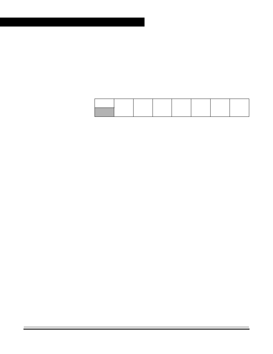
I/O Ports
Technical Data
MC68H(R)C08JL3
--
Rev. 4
140
I/O Ports
MOTOROLA
12.3.2 Data Direction Register A (DDRA)
Data direction register A determines whether each port A pin is an input
or an output. Writing a logic one to a DDRA bit enables the output buffer
for the corresponding port A pin; a logic zero disables the output buffer.
DDRA[6:0] -- Data Direction Register A Bits
These read/write bits control port A data direction. Reset clears
DDRA[6:0], configuring all port A pins as inputs.
1 = Corresponding port A pin configured as output
0 = Corresponding port A pin configured as input
NOTE:
Avoid glitches on port A pins by writing to the port A data register before
changing data direction register A bits from 0 to 1.
Figure 12-4
shows the port A I/O logic.
Address:
$0004
Bit 7
6
5
4
3
2
1
Bit 0
Read:
0
DDRA6
DDRA5
DDRA4
DDRA3
DDRA2
DDRA1
DDRA0
Write:
Reset:
0
0
0
0
0
0
0
0
Figure 12-3. Data Direction Register A (DDRA)
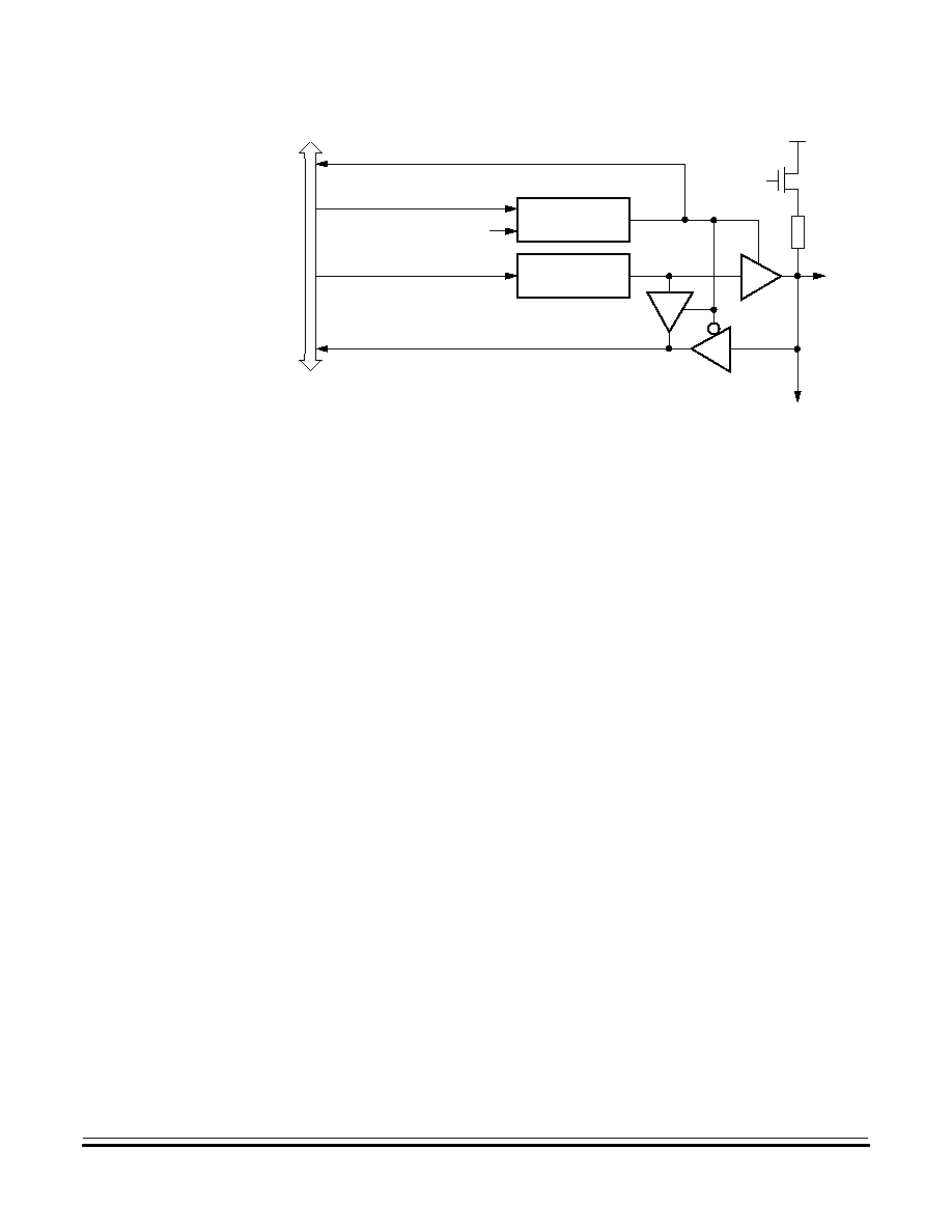
I/O Ports
Port A
MC68H(R)C08JL3
--
Rev. 4
Technical Data
MOTOROLA
I/O Ports
141
Figure 12-4. Port A I/O Circuit
When DDRAx is a logic 1, reading address $0000 reads the PTAx data
latch. When DDRAx is a logic 0, reading address $0000 reads the
voltage level on the pin. The data latch can always be written, regardless
of the state of its data direction bit.
12.3.3 Port A Input Pull-up Enable Register (PTAPUE)
The Port A Input Pull-up Enable Register (PTAPUE) contains a software
configurable pull-up device for each if the seven port A pins. Each bit is
individually configurable and requires the corresponding data direction
register, DDRAx be configured as input. Each pull-up device is
automatically and dynamically disabled when its corresponding DDRAx
bit is configured as output.
READ DDRA ($0004)
WRITE DDRA ($0004)
RESET
WRITE PTA ($0000)
READ PTA ($0000)
PTAx
DDRAx
PTAx
INTERNAL D
A
T
A
B
U
S
30k
PTAPUEx
To Keyboard Interrupt Circuit
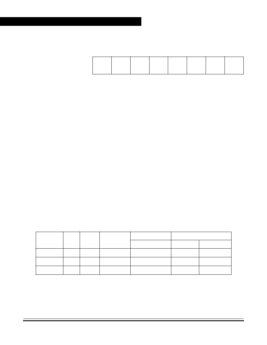
I/O Ports
Technical Data
MC68H(R)C08JL3
--
Rev. 4
142
I/O Ports
MOTOROLA
PTA6EN -- Enable PTA6 on OSC2
This read/write bit configures the OSC2 pin function when RC
oscillator option is selected. This bit has no effect for X-tal oscillator
option.
1 = OSC2 pin configured for PTA6 I/O, and has all the interrupt and
pull-up functions.
0 = OSC2 pin outputs the RC oscillator clock (RCCLK)
PTAPUE[6:0] -- Port A Input Pull-up Enable bits
These read/write bits are software programmable to enable pull-up
devices on port A pins
1 = Corresponding port A pin configured to have internal pull if its
DDRA bit is set to 0
0 = Pull-up device is disconnected on the corresponding port A pin
regardless of the state of its DDRA bit.
Table 12-1
summarizes the operation of the port B pins.
Address:
$000D
Bit 7
6
5
4
3
2
1
Bit 0
Read:
PTA6EN
PTAPUE6 PTAPUE5 PTAPUE4 PTAPUE3 PTAPUE2 PTAPUE2 PTAPUE0
Write:
Reset:
0
0
0
0
0
0
0
0
Figure 12-5. Port A Input Pull-up Enable Register (PTAPUE)
Table 12-1. Port A Pin Functions
PTAPUE Bit
DDRA
Bit
PTA Bit
I/O Pin Mode
Accesses to DDRB
Accesses to PTB
Read/Write
Read
Write
1
0
X
(1)
Input, V
DD
(2)
DDRA6-DDRA0
Pin
PTA6-PTA0
(3)
0
0
X
Input, Hi-Z
(4)
DDRA6-DDRA0
Pin
PTA6-PTA0
(3)
X
1
X
Output
DDRA6-DDRA0
PTA6-PTA0
PTA6-PTA0
1. X = Don't care.
2. I/O pin pulled to V
DD
by internal pull-up.
3. Writing affects data register, but does not affect input.
4. Hi-Z = High Impedence

I/O Ports
Port B
MC68H(R)C08JL3
--
Rev. 4
Technical Data
MOTOROLA
I/O Ports
143
12.4 Port B
Port B is an 8-bit special function port that shares all eight of its port pins
with the Analog-to-Digital converter (ADC) module, See
Section 11.
12.4.1 Port B Data Register (PTB)
The port B data register contains a data latch for each of the eight port B
pins.
PTB[7:0] -- Port B Data Bits
These read/write bits are software programmable. Data direction of
each port B pin is under the control of the corresponding bit in data
direction register B. Reset has no effect on port B data.
12.4.2 Data Direction Register B (DDRB)
Data direction register B determines whether each port B pin is an input
or an output. Writing a logic one to a DDRB bit enables the output buffer
for the corresponding port B pin; a logic zero disables the output buffer.
Address:
$0001
Bit 7
6
5
4
3
2
1
Bit 0
Read:
PTB7
PTB6
PTB5
PTB4
PTB3
PTB2
PTB1
PTB0
Write:
Reset:
Unaffected by reset
Alternative Function:
ADC7
ADC6
ADC5
ADC4
ADC3
ADC2
ADC2
ADC0
Figure 12-6. Port B Data Register (PTB)
Address:
$0005
Bit 7
6
5
4
3
2
1
Bit 0
Read:
DDRB7
DDRB6
DDRB5
DDRB4
DDRB3
DDRB2
DDRB1
DDRB0
Write:
Reset:
0
0
0
0
0
0
0
0
Figure 12-7. Data Direction Register B (DDRB)

I/O Ports
Technical Data
MC68H(R)C08JL3
--
Rev. 4
144
I/O Ports
MOTOROLA
DDRB[7:0] -- Data Direction Register B Bits
These read/write bits control port B data direction. Reset clears
DDRB[7:0], configuring all port B pins as inputs.
1 = Corresponding port B pin configured as output
0 = Corresponding port B pin configured as input
NOTE:
Avoid glitches on port B pins by writing to the port B data register before
changing data direction register B bits from 0 to 1.
Figure 12-8
shows
the port B I/O logic.
Figure 12-8. Port B I/O Circuit
When DDRBx is a logic 1, reading address $0001 reads the PTBx data
latch. When DDRBx is a logic 0, reading address $0001 reads the
voltage level on the pin. The data latch can always be written, regardless
of the state of its data direction bit.
Table 12-2
summarizes the operation
of the port B pins.
Table 12-2. Port B Pin Functions
DDRB Bit
PTB Bit
I/O Pin Mode
Accesses to DDRB
Accesses to PTB
Read/Write
Read
Write
0
X
(1)
1. X = don't care
Input, Hi-Z
(2)
2. Hi-Z = high impedance
DDRB7-DDRB0
Pin
PTB[7:0]
(3)
3. Writing affects data register, but does not affect the input.
1
X
Output
DDRB7-DDRB0
Pin
PTB[7:0]
READ DDRB ($0005)
WRITE DDRB ($0005)
RESET
WRITE PTB ($0001)
READ PTB ($0001)
PTBx
DDRBx
PTBx
INTERNAL D
A
T
A
B
U
S
To Analog-To-Digital Converter

I/O Ports
Port D
MC68H(R)C08JL3
--
Rev. 4
Technical Data
MOTOROLA
I/O Ports
145
12.5 Port D
Port D is an 8-bit special function port that shares two of its pins with
Timer Interface Module, (see
Section 10.
) and shares four of its pins
with Analog to Digital Conversion Module (see
Section 11.
). PTD6 and
PTD7 each has high current drive (25mA sink) and programmable pull-
up. PTD2, PTD3, PTD6 and PTD7 each has LED driving capability.
12.5.1 Port D Data Register (PTD)
The port D data register contains a data latch for each of the eight port D
pins.
PTD[7:0] -- Port D Data Bits
These read/write bits are software programmable. Data direction of
each port D pin is under the control of the corresponding bit in data
direction register D. Reset has no effect on port D data.
Address:
$0003
Bit 7
6
5
4
3
2
1
Bit 0
Read:
PTD7
PTD6
PTD5
PTD4
PTD3
PTD2
PTD1
PTD0
Write:
Reset:
Additional Functions
LED
LED
LED
LED
ADC8
ADC9
ADC10
ADC11
TCH1
TCH0
25mA sink
(Slow Edge)
25mA sink
(Slow Edge)
5k pull-up 5k pull-up
Figure 12-9. Port D Data Register (PTD)

I/O Ports
Technical Data
MC68H(R)C08JL3
--
Rev. 4
146
I/O Ports
MOTOROLA
12.5.2 Data Direction Register D (DDRD)
Data direction register D determines whether each port D pin is an input
or an output. Writing a logic one to a DDRD bit enables the output buffer
for the corresponding port D pin; a logic zero disables the output buffer.
DDRD[7:0] -- Data Direction Register D Bits
These read/write bits control port D data direction. Reset clears
DDRD[7:0], configuring all port D pins as inputs.
1 = Corresponding port D pin configured as output
0 = Corresponding port D pin configured as input
NOTE:
Avoid glitches on port D pins by writing to the port D data register before
changing data direction register D bits from 0 to 1.
Figure 12-11
shows
the port D I/O logic.
Figure 12-11. Port D I/O Circuit
Address:
$0007
Bit 7
6
5
4
3
2
1
Bit 0
Read:
DDRD7
DDRD6
DDRD5
DDRD4
DDRD3
DDRD2
DDRD1
DDRD0
Write:
Reset:
0
0
0
0
0
0
0
0
Figure 12-10. Data Direction Register D (DDRD)
READ DDRD ($0007)
WRITE DDRD ($0007)
RESET
WRITE PTD ($0003)
READ PTD ($0003)
PTDx
DDRDx
PTDx
INTERNAL D
A
T
A
B
U
S
PTD[0:3] To Analog-To-Digital Converter
5k
PTDPU[6:7]
PTD[4:5] To Timer
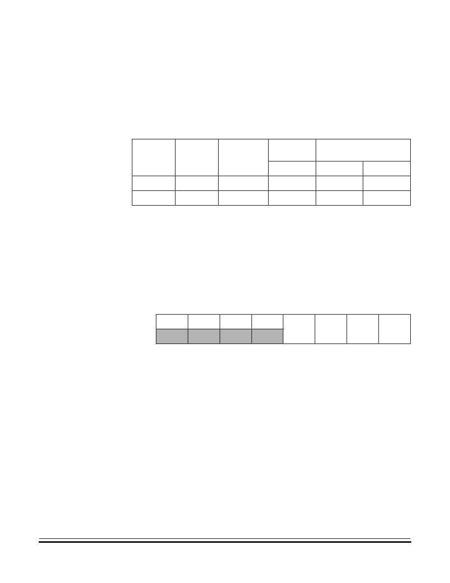
I/O Ports
Port D
MC68H(R)C08JL3
--
Rev. 4
Technical Data
MOTOROLA
I/O Ports
147
When DDRDx is a logic 1, reading address $0003 reads the PTDx data
latch. When DDRDx is a logic 0, reading address $0003 reads the
voltage level on the pin. The data latch can always be written, regardless
of the state of its data direction bit.
Table 12-3
summarizes the operation
of the port D pins.
12.5.3 Port D Control Register (PDCR)
The Port D Control Register enables/disables the pull-up resistor and
slow-edge high current capability of pins PTD6 and PTD7.
SLOWDx -- Slow Edge Enable
The SLOWD6 and SLOWD7 bits enable the Slow-edge, open-drain,
high current output (25mA sink) of port pins PTD6 and PTD7
respectively. DDRx bit is not affected by SLOWDx.
1 = Slow edge enabled; pin is open-drain output
0 = Slow edge disabled; pin is push-pull
PTDPUx -- Pull-up Enable
The PTDPU6 and PTDPU7 bits enable the 5k pull-up on PTD6 and
PTD7 respectively, regardless the status of DDRDx bit.
1 = Enable 5k pull-up
0 = Disable 5k pull-up
Table 12-3. Port D Pin Functions
DDRD
Bit
PTD Bit
I/O Pin
Mode
Accesses
to DDRA
Accesses to PTD
Read/Write
Read
Write
0
X
(1)
1. X = don't care
Input, Hi-Z
(2)
2. Hi-Z = high impedance
DDRD[7:0]
Pin
PTD[7:0]
(3)
3. Writing affects data register, but does not affect the input.
1
X
Output
DDRD[7:0]
Pin
PTD[7:0]
Address:
$000A
Bit 7
6
5
4
3
2
1
Bit 0
Read:
0
0
0
0
SLOWD7
SLOWD6
PTDPU7
PTDPU6
Write:
Reset:
0
0
0
0
0
0
0
0
Figure 12-12. Port D Control Register (PDCR)

I/O Ports
Technical Data
MC68H(R)C08JL3
--
Rev. 4
148
I/O Ports
MOTOROLA

MC68H(R)C08JL3
--
Rev. 4
Technical Data
MOTOROLA
External Interrupt (IRQ)
149
Technical Data -- MC68H(R)C08JL3
Section 13. External Interrupt (IRQ)
13.1 Contents
13.2
Introduction . . . . . . . . . . . . . . . . . . . . . . . . . . . . . . . . . . . . . . . 149
13.3
Features . . . . . . . . . . . . . . . . . . . . . . . . . . . . . . . . . . . . . . . . . 149
13.4
Functional Description . . . . . . . . . . . . . . . . . . . . . . . . . . . . . . 150
13.4.1
IRQ1 Pin. . . . . . . . . . . . . . . . . . . . . . . . . . . . . . . . . . . . . . . 151
13.5
IRQ Module During Break Interrupts . . . . . . . . . . . . . . . . . . . 153
13.6
IRQ Status and Control Register (ISCR) . . . . . . . . . . . . . . . . 153
13.2 Introduction
The IRQ (external interrupt) module provides a maskable interrupt input.
13.3 Features
Features of the IRQ module include the following:
∑
A dedicated external interrupt pin, IRQ1
∑
IRQ1 interrupt control bits
∑
Hysteresis buffer
∑
Programmable edge-only or edge and level interrupt sensitivity
∑
Automatic interrupt acknowledge
∑
Selectable internal pullup resistor

External Interrupt (IRQ)
Technical Data
MC68H(R)C08JL3
--
Rev. 4
150
External Interrupt (IRQ)
MOTOROLA
13.4 Functional Description
A logic zero applied to the external interrupt pin can latch a CPU interrupt
request.
Figure 13-1
shows the structure of the IRQ module.
Interrupt signals on the IRQ1 pin are latched into the IRQ1 latch. An
interrupt latch remains set until one of the following actions occurs:
∑
Vector fetch -- A vector fetch automatically generates an interrupt
acknowledge signal that clears the IRQ latch.
∑
Software clear -- Software can clear the interrupt latch by writing
to the acknowledge bit in the interrupt status and control register
(ISCR). Writing a logic one to the ACK1 bit clears the IRQ1 latch.
∑
Reset -- A reset automatically clears the interrupt latch.
The external interrupt pin is falling-edge-triggered and is software-
configurable to be either falling-edge or falling-edge and low-level-
triggered. The MODE1 bit in the ISCR controls the triggering sensitivity
of the IRQ1 pin.
When the interrupt pin is edge-triggered only, the CPU interrupt request
remains set until a vector fetch, software clear, or reset occurs.
When the interrupt pin is both falling-edge and low-level-triggered, the
CPU interrupt request remains set until both of the following occur:
∑
Vector fetch or software clear
∑
Return of the interrupt pin to logic one
The vector fetch or software clear may occur before or after the interrupt
pin returns to logic one. As long as the pin is low, the interrupt request
remains pending. A reset will clear the latch and the MODE1 control bit,
thereby clearing the interrupt even if the pin stays low.
When set, the IMASK1 bit in the ISCR mask all external interrupt
requests. A latched interrupt request is not presented to the interrupt
priority logic unless the IMASK1 bit is clear.

External Interrupt (IRQ)
Functional Description
MC68H(R)C08JL3
--
Rev. 4
Technical Data
MOTOROLA
External Interrupt (IRQ)
151
NOTE:
The interrupt mask (I) in the condition code register (CCR) masks all
interrupt requests, including external interrupt requests.
(See
7.6
Exception Control
.)
Figure 13-1. IRQ Module Block Diagram
13.4.1 IRQ1 Pin
A logic zero on the IRQ1 pin can latch an interrupt request into the IRQ1
latch. A vector fetch, software clear, or reset clears the IRQ1 latch.
If the MODE1 bit is set, the IRQ1 pin is both falling-edge-sensitive and
low-level-sensitive. With MODE1 set, both of the following actions must
occur to clear IRQ1:
ACK1
IMASK1
D
Q
CK
CLR
IRQ1
HIGH
INTERRUPT
TO MODE
SELECT
LOGIC
IRQ1
FF
REQUEST
V
DD
MODE1
VOLTAGE
DETECT
SYNCHRO-
NIZER
IRQF1
TO CPU FOR
BIL/BIH
INSTRUCTIONS
VECTOR
FETCH
DECODER
INTERNAL ADDRESS BUS
RESET
V
DD
I
NTERNAL
PULLUP
DEVICE
IRQ1
IRQPUD
Addr.
Register Name
Bit 7
6
5
4
3
2
1
Bit 0
$001D
IRQ Status and Control
Register
(INTSCR)
Read:
0
0
0
0
IRQF1
0
IMASK1
MODE1
Write:
ACK1
Reset:
0
0
0
0
0
0
0
0
= Unimplemented
Figure 13-2. IRQ I/O Register Summary

External Interrupt (IRQ)
Technical Data
MC68H(R)C08JL3
--
Rev. 4
152
External Interrupt (IRQ)
MOTOROLA
∑
Vector fetch or software clear -- A vector fetch generates an
interrupt acknowledge signal to clear the latch. Software may
generate the interrupt acknowledge signal by writing a logic one to
the ACK1 bit in the interrupt status and control register (ISCR).
The ACK1 bit is useful in applications that poll the IRQ1 pin and
require software to clear the IRQ1 latch. Writing to the ACK1 bit
prior to leaving an interrupt service routine can also prevent
spurious interrupts due to noise. Setting ACK1 does not affect
subsequent transitions on the IRQ1 pin. A falling edge that occurs
after writing to the ACK1 bit latches another interrupt request. If
the IRQ1 mask bit, IMASK1, is clear, the CPU loads the program
counter with the vector address at locations $FFFA and $FFFB.
∑
Return of the IRQ1 pin to logic one -- As long as the IRQ1 pin is
at logic zero, IRQ1 remains active.
The vector fetch or software clear and the return of the IRQ1 pin to logic
one may occur in any order. The interrupt request remains pending as
long as the IRQ1 pin is at logic zero. A reset will clear the latch and the
MODE1 control bit, thereby clearing the interrupt even if the pin stays
low.
If the MODE1 bit is clear, the IRQ1 pin is falling-edge-sensitive only.
With MODE1 clear, a vector fetch or software clear immediately clears
the IRQ1 latch.
The IRQF1 bit in the ISCR register can be used to check for pending
interrupts. The IRQF1 bit is not affected by the IMASK1 bit, which makes
it useful in applications where polling is preferred.
Use the BIH or BIL instruction to read the logic level on the IRQ1 pin.
NOTE:
When using the level-sensitive interrupt trigger, avoid false interrupts by
masking interrupt requests in the interrupt routine.
NOTE:
An internal pull-up resistor to V
DD
is connected to the IRQ1 pin; this can
be disabled by setting the IRQPUD bit in the CONFIG2 register ($001E).

External Interrupt (IRQ)
IRQ Module During Break Interrupts
MC68H(R)C08JL3
--
Rev. 4
Technical Data
MOTOROLA
External Interrupt (IRQ)
153
13.5 IRQ Module During Break Interrupts
The system integration module (SIM) controls whether the IRQ1 latch
can be cleared during the break state. The BCFE bit in the break flag
control register (BFCR) enables software to clear the latches during the
break state.
(See Section 7. System Integration Module (SIM)
.)
To allow software to clear the IRQ1 latch during a break interrupt, write
a logic one to the BCFE bit. If a latch is cleared during the break state, it
remains cleared when the MCU exits the break state.
To protect the latches during the break state, write a logic zero to the
BCFE bit. With BCFE at logic zero (its default state), writing to the ACK1
bit in the IRQ status and control register during the break state has no
effect on the IRQ latch.
13.6 IRQ Status and Control Register (ISCR)
The IRQ Status and Control Register (ISCR) controls and monitors
operation of the IRQ module. The ISCR has the following functions:
∑
Shows the state of the IRQ1 flag
∑
Clears the IRQ1 latch
∑
Masks IRQ1 and interrupt request
∑
Controls triggering sensitivity of the IRQ1 interrupt pin
Address:
$001D
Bit 7
6
5
4
3
2
1
Bit 0
Read:
0
0
0
0
IRQF1
IMASK1
MODE1
Write:
ACK1
Reset:
0
0
0
0
0
0
0
0
= Unimplemented
Figure 13-3. IRQ Status and Control Register (INTSCR)

External Interrupt (IRQ)
Technical Data
MC68H(R)C08JL3
--
Rev. 4
154
External Interrupt (IRQ)
MOTOROLA
IRQF1 -- IRQ1 Flag
This read-only status bit is high when the IRQ1 interrupt is pending.
1 = IRQ1 interrupt pending
0 = IRQ1 interrupt not pending
ACK1 -- IRQ1 Interrupt Request Acknowledge Bit
Writing a logic one to this write-only bit clears the IRQ1 latch. ACK1
always reads as logic zero. Reset clears ACK1.
IMASK1 -- IRQ1 Interrupt Mask Bit
Writing a logic one to this read/write bit disables IRQ1 interrupt
requests. Reset clears IMASK1.
1 = IRQ1 interrupt requests disabled
0 = IRQ1 interrupt requests enabled
MODE1 -- IRQ1 Edge/Level Select Bit
This read/write bit controls the triggering sensitivity of the IRQ1 pin.
Reset clears MODE1.
1 = IRQ1 interrupt requests on falling edges and low levels
0 = IRQ1 interrupt requests on falling edges only
IRQPUD -- IRQ1 Pin Pull-up control bit
1 = Internal pull-up is disconnected
0 = Internal pull-up is connected between IRQ1 pin and V
DD
Address:
$001E
Bit 7
6
5
4
3
2
1
Bit 0
Read:
IRQPUD
R
R
LVIT1
LVIT0
R
R
R
Write:
Reset:
0
0
0
Not affected
Not affected
0
0
0
POR:
0
0
0
0
0
0
0
0
R
= Reserved
Figure 13-4. Configuration Register 2 (CONFIG2)

MC68H(R)C08JL3
--
Rev. 4
Technical Data
MOTOROLA
Keyboard Interrupt Module (KBI)
155
Technical Data -- MC68H(R)C08JL3
Section 14. Keyboard Interrupt Module (KBI)
14.1 Contents
14.2
Introduction . . . . . . . . . . . . . . . . . . . . . . . . . . . . . . . . . . . . . . . 155
14.3
Features . . . . . . . . . . . . . . . . . . . . . . . . . . . . . . . . . . . . . . . . . 155
14.4
Functional Description . . . . . . . . . . . . . . . . . . . . . . . . . . . . . . 156
14.4.1
Keyboard Initialization . . . . . . . . . . . . . . . . . . . . . . . . . . . . 158
14.4.2
Keyboard Status and Control Register. . . . . . . . . . . . . . . . 159
14.4.3
Keyboard Interrupt Enable Register . . . . . . . . . . . . . . . . . . 160
14.5
Wait Mode. . . . . . . . . . . . . . . . . . . . . . . . . . . . . . . . . . . . . . . . 161
14.6
Stop Mode . . . . . . . . . . . . . . . . . . . . . . . . . . . . . . . . . . . . . . . 161
14.7
Keyboard Module During Break Interrupts . . . . . . . . . . . . . . . 161
14.2 Introduction
The keyboard interrupt module (KBI) provides seven independently
maskable external interrupts which are accessible via PTA0≠PTA6 pins.
14.3 Features
Features of the keyboard interrupt module include the following:
∑
Seven keyboard interrupt pins with separate keyboard interrupt
enable bits and one keyboard interrupt mask
∑
Software configurable pull-up device if input pin is configured as
input port bit
∑
Programmable edge-only or edge- and level- interrupt sensitivity
∑
Exit from low-power modes
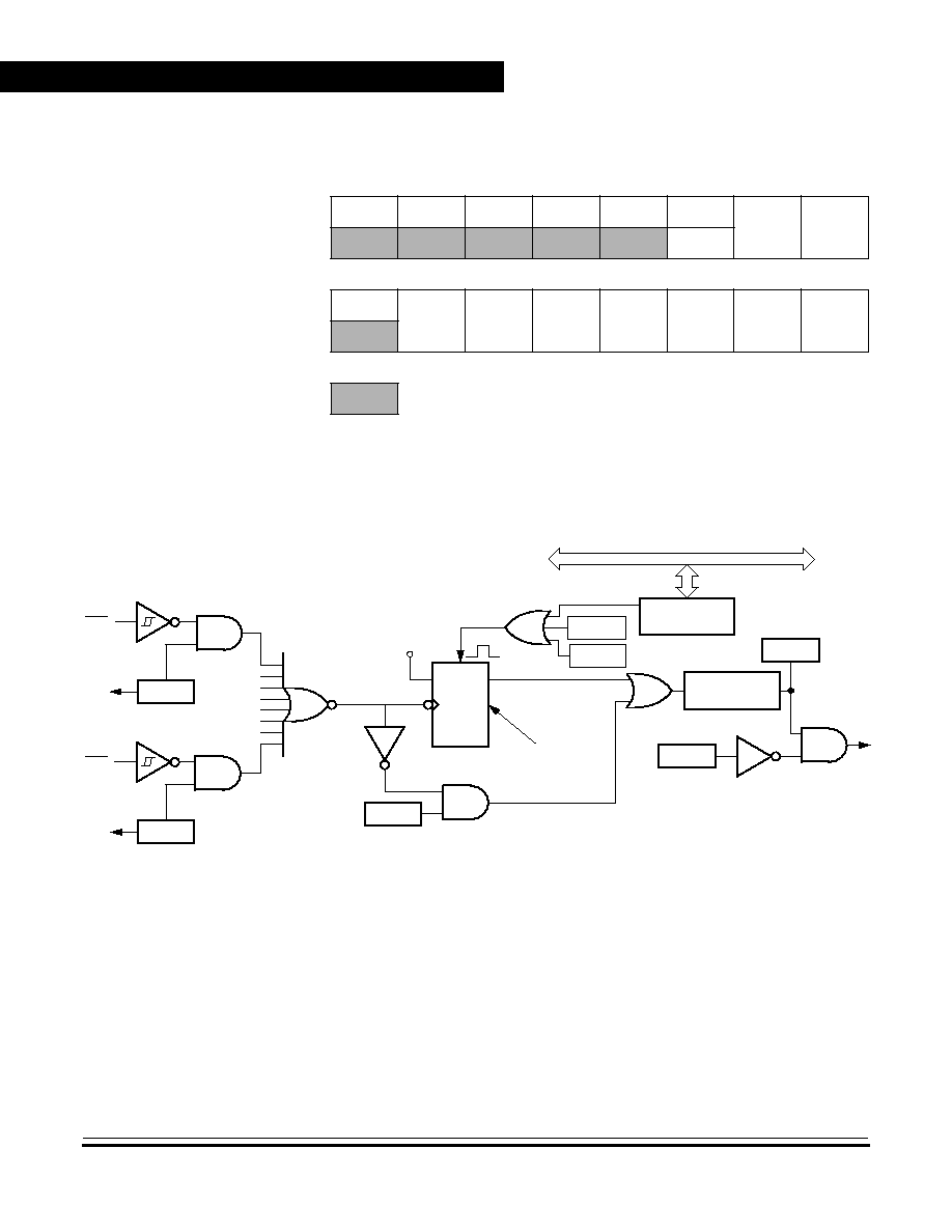
Keyboard Interrupt Module (KBI)
Technical Data
MC68H(R)C08JL3
--
Rev. 4
156
Keyboard Interrupt Module (KBI)
MOTOROLA
14.4 Functional Description
Figure 14-2. Keyboard Interrupt Block Diagram
Writing to the KBIE6≠KBIE0 bits in the keyboard interrupt enable register
independently enables or disables each port A pin as a keyboard
interrupt pin. Enabling a keyboard interrupt pin in port A also enables its
internal pull-up device irrespective of PTAPUEx bits in the port A input
pull-up enable register (see
12.3.3
). A logic 0 applied to an enabled
keyboard interrupt pin latches a keyboard interrupt request.
Addr.
Register Name
Bit 7
6
5
4
3
2
1
Bit 0
$001A
Keyboard Status
and Control Register
(KBSCR)
Read:
0
0
0
0
KEYF
0
IMASKK
MODEK
Write:
ACKK
Reset:
0
0
0
0
0
0
0
0
$001B
Keyboard Interrupt Enable
Register (KBIER)
Read:
0
KBIE6
KBIE5
KBIE4
KBIE3
KBIE2
KBIE1
KBIE0
Write:
Reset:
0
0
0
0
0
0
0
0
= Unimplemented
Figure 14-1. KBI I/O Register Summary
KBIE0
KBIE6
.
.
.
D
Q
CK
CLR
V
DD
MODEK
IMASKK
KEYBOARD
INTERRUPT FF
VECTOR FETCH
DECODER
ACKK
INTERNAL BUS
RESET
KBI6
KBI0
SYNCHRONIZER
KEYF
Keyboard
Interrupt
Request
TO PULLUP ENABLE
TO PULLUP ENABLE

Keyboard Interrupt Module (KBI)
Functional Description
MC68H(R)C08JL3
--
Rev. 4
Technical Data
MOTOROLA
Keyboard Interrupt Module (KBI)
157
A keyboard interrupt is latched when one or more keyboard pins goes
low after all were high. The MODEK bit in the keyboard status and
control register controls the triggering mode of the keyboard interrupt.
∑
If the keyboard interrupt is edge-sensitive only, a falling edge on a
keyboard pin does not latch an interrupt request if another
keyboard pin is already low. To prevent losing an interrupt request
on one pin because another pin is still low, software can disable
the latter pin while it is low.
∑
If the keyboard interrupt is falling edge- and low level-sensitive, an
interrupt request is present as long as any keyboard pin is low.
If the MODEK bit is set, the keyboard interrupt pins are both falling edge-
and low level-sensitive, and both of the following actions must occur to
clear a keyboard interrupt request:
∑
Vector fetch or software clear -- A vector fetch generates an
interrupt acknowledge signal to clear the interrupt request.
Software may generate the interrupt acknowledge signal by
writing a logic 1 to the ACKK bit in the keyboard status and control
register KBSCR. The ACKK bit is useful in applications that poll
the keyboard interrupt pins and require software to clear the
keyboard interrupt request. Writing to the ACKK bit prior to leaving
an interrupt service routine can also prevent spurious interrupts
due to noise. Setting ACKK does not affect subsequent transitions
on the keyboard interrupt pins. A falling edge that occurs after
writing to the ACKK bit latches another interrupt request. If the
keyboard interrupt mask bit, IMASKK, is clear, the CPU loads the
program counter with the vector address at locations $FFE0 and
$FFE1.
∑
Return of all enabled keyboard interrupt pins to logic 1 -- As long
as any enabled keyboard interrupt pin is at logic 0, the keyboard
interrupt remains set.
The vector fetch or software clear and the return of all enabled keyboard
interrupt pins to logic 1 may occur in any order.

Keyboard Interrupt Module (KBI)
Technical Data
MC68H(R)C08JL3
--
Rev. 4
158
Keyboard Interrupt Module (KBI)
MOTOROLA
If the MODEK bit is clear, the keyboard interrupt pin is falling-edge-
sensitive only. With MODEK clear, a vector fetch or software clear
immediately clears the keyboard interrupt request.
Reset clears the keyboard interrupt request and the MODEK bit, clearing
the interrupt request even if a keyboard interrupt pin stays at logic 0.
The keyboard flag bit (KEYF) in the keyboard status and control register
can be used to see if a pending interrupt exists. The KEYF bit is not
affected by the keyboard interrupt mask bit (IMASKK) which makes it
useful in applications where polling is preferred.
To determine the logic level on a keyboard interrupt pin, disable the pull-
up device, use the data direction register to configure the pin as an input
and then read the data register.
NOTE:
Setting a keyboard interrupt enable bit (KBIEx) forces the corresponding
keyboard interrupt pin to be an input, overriding the data direction
register. However, the data direction register bit must be a logic 0 for
software to read the pin.
14.4.1 Keyboard Initialization
When a keyboard interrupt pin is enabled, it takes time for the internal
pull-up to reach a logic 1. Therefore a false interrupt can occur as soon
as the pin is enabled.
To prevent a false interrupt on keyboard initialization:
1. Mask keyboard interrupts by setting the IMASKK bit in the
keyboard status and control register.
2. Enable the KBI pins by setting the appropriate KBIEx bits in the
keyboard interrupt enable register.
3. Write to the ACKK bit in the keyboard status and control register
to clear any false interrupts.
4. Clear the IMASKK bit.
An interrupt signal on an edge-triggered pin can be acknowledged
immediately after enabling the pin. An interrupt signal on an edge- and

Keyboard Interrupt Module (KBI)
Functional Description
MC68H(R)C08JL3
--
Rev. 4
Technical Data
MOTOROLA
Keyboard Interrupt Module (KBI)
159
level-triggered interrupt pin must be acknowledged after a delay that
depends on the external load.
Another way to avoid a false interrupt:
1. Configure the keyboard pins as outputs by setting the appropriate
DDRA bits in the data direction register A.
2. Write logic 1s to the appropriate port A data register bits.
3. Enable the KBI pins by setting the appropriate KBIEx bits in the
keyboard interrupt enable register.
14.4.2 Keyboard Status and Control Register
∑
Flags keyboard interrupt requests.
∑
Acknowledges keyboard interrupt requests.
∑
Masks keyboard interrupt requests.
∑
Controls keyboard interrupt triggering sensitivity.
Bits 7≠4 -- Not used
These read-only bits always read as logic 0s.
KEYF -- Keyboard Flag Bit
This read-only bit is set when a keyboard interrupt is pending on port-
A. Reset clears the KEYF bit.
1 = Keyboard interrupt pending
0 = No keyboard interrupt pending
Address:
$001A
Bit 7
6
5
4
3
2
1
Bit 0
Read:
0
0
0
0
KEYF
0
IMASKK
MODEK
Write:
ACKK
Reset:
0
0
0
0
0
0
0
0
= Unimplemented
Figure 14-3. Keyboard Status and Control Register (KBSCR)

Keyboard Interrupt Module (KBI)
Technical Data
MC68H(R)C08JL3
--
Rev. 4
160
Keyboard Interrupt Module (KBI)
MOTOROLA
ACKK -- Keyboard Acknowledge Bit
Writing a logic 1 to this write-only bit clears the keyboard interrupt
request on port-A. ACKK always reads as logic 0. Reset clears ACKK.
IMASKK-- Keyboard Interrupt Mask Bit
Writing a logic 1 to this read/write bit prevents the output of the
keyboard interrupt mask from generating interrupt requests on port-A.
Reset clears the IMASKK bit.
1 = Keyboard interrupt requests masked
0 = Keyboard interrupt requests not masked
MODEK -- Keyboard Triggering Sensitivity Bit
This read/write bit controls the triggering sensitivity of the keyboard
interrupt pins on port-A. Reset clears MODEK.
1 = Keyboard interrupt requests on falling edges and low levels
0 = Keyboard interrupt requests on falling edges only
14.4.3 Keyboard Interrupt Enable Register
The port-A keyboard interrupt enable register enables or disables each
port-A pin to operate as a keyboard interrupt pin.
KBIE6≠KBIE0 -- Port-A Keyboard Interrupt Enable Bits
Each of these read/write bits enables the corresponding keyboard
interrupt pin on port-A to latch interrupt requests. Reset clears the
keyboard interrupt enable register.
1 = KBIx pin enabled as keyboard interrupt pin
0 = KBIx pin not enabled as keyboard interrupt pin
Address:
$001B
Bit 7
6
5
4
3
2
1
Bit 0
Read:
0
KBIE6
KBIE5
KBIE4
KBIE3
KBIE2
KBIE1
KBIE0
Write:
Reset:
0
0
0
0
0
0
0
0
Figure 14-4. Keyboard Interrupt Enable Register (KBIER)

Keyboard Interrupt Module (KBI)
Wait Mode
MC68H(R)C08JL3
--
Rev. 4
Technical Data
MOTOROLA
Keyboard Interrupt Module (KBI)
161
14.5 Wait Mode
The keyboard modules remain active in wait mode. Clearing the
IMASKK bit in the keyboard status and control register enables keyboard
interrupt requests to bring the MCU out of wait mode.
14.6 Stop Mode
The keyboard module remains active in stop mode. Clearing the
IMASKK bit in the keyboard status and control register enables keyboard
interrupt requests to bring the MCU out of stop mode.
14.7 Keyboard Module During Break Interrupts
The system integration module (SIM) controls whether the keyboard
interrupt latch can be cleared during the break state. The BCFE bit in the
break flag control register (BFCR) enables software to clear status bits
during the break state.
To allow software to clear the keyboard interrupt latch during a break
interrupt, write a logic 1 to the BCFE bit. If a latch is cleared during the
break state, it remains cleared when the MCU exits the break state.
To protect the latch during the break state, write a logic 0 to the BCFE
bit. With BCFE at logic 0 (its default state), writing to the keyboard
acknowledge bit (ACKK) in the keyboard status and control register
during the break state has no effect.

Keyboard Interrupt Module (KBI)
Technical Data
MC68H(R)C08JL3
--
Rev. 4
162
Keyboard Interrupt Module (KBI)
MOTOROLA

MC68H(R)C08JL3
--
Rev. 4
Technical Data
MOTOROLA
Computer Operating Properly (COP)
163
Technical Data -- MC68H(R)C08JL3
Section 15. Computer Operating Properly (COP)
15.1 Contents
15.2
Introduction . . . . . . . . . . . . . . . . . . . . . . . . . . . . . . . . . . . . . . . 163
15.3
Functional Description . . . . . . . . . . . . . . . . . . . . . . . . . . . . . . 164
15.4
I/O Signals . . . . . . . . . . . . . . . . . . . . . . . . . . . . . . . . . . . . . . . 165
15.4.1
2OSCOUT . . . . . . . . . . . . . . . . . . . . . . . . . . . . . . . . . . . . . 165
15.4.2
COPCTL Write . . . . . . . . . . . . . . . . . . . . . . . . . . . . . . . . . . 165
15.4.3
Power-On Reset. . . . . . . . . . . . . . . . . . . . . . . . . . . . . . . . . 165
15.4.4
Internal Reset . . . . . . . . . . . . . . . . . . . . . . . . . . . . . . . . . . . 165
15.4.5
Reset Vector Fetch. . . . . . . . . . . . . . . . . . . . . . . . . . . . . . . 166
15.4.6
COPD (COP Disable). . . . . . . . . . . . . . . . . . . . . . . . . . . . . 166
15.4.7
COPRS (COP Rate Select) . . . . . . . . . . . . . . . . . . . . . . . . 166
15.5
COP Control Register . . . . . . . . . . . . . . . . . . . . . . . . . . . . . . . 167
15.6
Interrupts. . . . . . . . . . . . . . . . . . . . . . . . . . . . . . . . . . . . . . . . . 167
15.7
Monitor Mode . . . . . . . . . . . . . . . . . . . . . . . . . . . . . . . . . . . . . 167
15.8
Low-Power Modes . . . . . . . . . . . . . . . . . . . . . . . . . . . . . . . . . 167
15.8.1
Wait Mode . . . . . . . . . . . . . . . . . . . . . . . . . . . . . . . . . . . . . 167
15.8.2
Stop Mode . . . . . . . . . . . . . . . . . . . . . . . . . . . . . . . . . . . . . 168
15.9
COP Module During Break Mode . . . . . . . . . . . . . . . . . . . . . . 168
15.2 Introduction
The computer operating properly (COP) module contains a free-running
counter that generates a reset if allowed to overflow. The COP module
helps software recover from runaway code. Prevent a COP reset by
clearing the COP counter periodically. The COP module can be disabled
through the COPD bit in the CONFIG1 register.
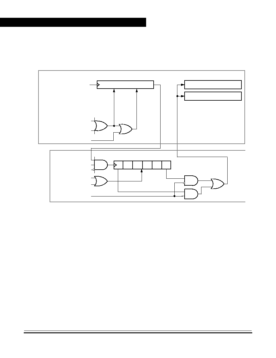
Computer Operating Properly (COP)
Technical Data
MC68H(R)C08JL3
--
Rev. 4
164
Computer Operating Properly (COP)
MOTOROLA
15.3 Functional Description
Figure 15-1
shows the structure of the COP module.
Figure 15-1. COP Block Diagram
The COP counter is a free-running 6-bit counter preceded by the 12-bit
system integration module (SIM) counter. If not cleared by software, the
COP counter overflows and generates an asynchronous reset after
2
18
≠ 2
4
or 2
13
≠ 2
4
2OSCOUT cycles; depending on the state of the
COP rate select bit, COPRS, in configuration register 1. With a 2
18
≠ 2
4
2OSCOUT cycle overflow option, a 8MHz crystal gives a COP timeout
period of 32.766 ms. Writing any value to location $FFFF before an
overflow occurs prevents a COP reset by clearing the COP counter and
stages 12 through 5 of the SIM counter.
COPCTL WRITE
2OSCOUT
RESET VECTOR FETCH
SIM RESET CIRCUIT
RESET STATUS REGISTER
INTERNAL RESET SOURCES
(1)
SIM
CLEAR STAGES 5≠12
12-BIT SIM COUNTER
CLEAR ALL STAGES
COPD (FROM CONFIG1)
RESET
COPCTL WRITE
CLEAR
COP MODULE
COPEN (FROM SIM)
COP COUNTER
NOTE:
1. See SIM section for more details.
COP CLOCK
COP TIMEOUT
COP RATE SEL
(COPRS FROM CONFIG1)
6-BIT COP COUNTER

Computer Operating Properly (COP)
I/O Signals
MC68H(R)C08JL3
--
Rev. 4
Technical Data
MOTOROLA
Computer Operating Properly (COP)
165
NOTE:
Service the COP immediately after reset and before entering or after
exiting stop mode to guarantee the maximum time before the first COP
counter overflow.
A COP reset pulls the RST pin low for 32
◊
2OSCOUT cycles and sets
the COP bit in the reset status register (RSR). (See
7.8.2 Reset Status
Register (RSR)
.).
NOTE:
Place COP clearing instructions in the main program and not in an
interrupt subroutine. Such an interrupt subroutine could keep the COP
from generating a reset even while the main program is not working
properly.
15.4 I/O Signals
The following paragraphs describe the signals shown in
Figure 15-1
.
15.4.1 2OSCOUT
2OSCOUT is the oscillator output signal. 2OSCOUT frequency is equal
to the crystal frequency or the RC-oscillator frequency.
15.4.2 COPCTL Write
Writing any value to the COP control register (COPCTL)
(see 15.5 COP
Control Register
) clears the COP counter and clears bits 12 through 5
of the SIM counter. Reading the COP control register returns the low
byte of the reset vector.
15.4.3 Power-On Reset
The power-on reset (POR) circuit in the SIM clears the SIM counter
4096
◊
2OSCOUT cycles after power-up.
15.4.4 Internal Reset
An internal reset clears the SIM counter and the COP counter.

Computer Operating Properly (COP)
Technical Data
MC68H(R)C08JL3
--
Rev. 4
166
Computer Operating Properly (COP)
MOTOROLA
15.4.5 Reset Vector Fetch
A reset vector fetch occurs when the vector address appears on the data
bus. A reset vector fetch clears the SIM counter.
15.4.6 COPD (COP Disable)
The COPD signal reflects the state of the COP disable bit (COPD) in the
configuration register (CONFIG). (See
Section 5. Configuration
Register (CONFIG)
.)
15.4.7 COPRS (COP Rate Select)
The COPRS signal reflects the state of the COP rate select bit (COPRS)
in the configuration register 1.
COPRS -- COP Rate Select Bit
COPRS selects the COP timeout period. Reset clears COPRS.
1 = COP timeout period is (2
13
≠ 2
4
)
◊
2OSCOUT cycles
0 = COP timeout period is (2
18
≠ 2
4
)
◊
2OSCOUT cycles
COPD -- COP Disable Bit
COPD disables the COP module.
1 = COP module disabled
0 = COP module enabled
Address:
$001F
Bit 7
6
5
4
3
2
1
Bit 0
Read:
COPRS
R
R
LVID
R
SSREC
STOP
COPD
Write:
Reset:
0
0
0
0
0
0
0
0
R
= Reserved
Figure 15-2. Configuration Register 1 (CONFIG1)

Computer Operating Properly (COP)
COP Control Register
MC68H(R)C08JL3
--
Rev. 4
Technical Data
MOTOROLA
Computer Operating Properly (COP)
167
15.5 COP Control Register
The COP control register is located at address $FFFF and overlaps the
reset vector. Writing any value to $FFFF clears the COP counter and
starts a new timeout period. Reading location $FFFF returns the low
byte of the reset vector.
15.6 Interrupts
The COP does not generate CPU interrupt requests.
15.7 Monitor Mode
The COP is disabled in monitor mode when V
DD
+ V
HI
is present on the
IRQ1 pin or on the RST pin.
15.8 Low-Power Modes
The WAIT and STOP instructions put the MCU in low-power
consumption standby modes.
15.8.1 Wait Mode
The COP continues to operate during wait mode. To prevent a COP
reset during wait mode, periodically clear the COP counter in a CPU
interrupt routine.
Address:
$FFFF
Bit 7
6
5
4
3
2
1
Bit 0
Read:
Low byte of reset vector
Write:
Clear COP counter
Reset:
Unaffected by reset
Figure 15-3. COP Control Register (COPCTL)

Computer Operating Properly (COP)
Technical Data
MC68H(R)C08JL3
--
Rev. 4
168
Computer Operating Properly (COP)
MOTOROLA
15.8.2 Stop Mode
Stop mode turns off the 2OSCOUT input to the COP and clears the SIM
counter. Service the COP immediately before entering or after exiting
stop mode to ensure a full COP timeout period after entering or exiting
stop mode.
15.9 COP Module During Break Mode
The COP is disabled during a break interrupt when V
DD
+ V
HI
is present
on the RST pin.

MC68H(R)C08JL3
--
Rev. 4
Technical Data
MOTOROLA
Low Voltage Inhibit (LVI)
169
Technical Data -- MC68H(R)C08JL3
Section 16. Low Voltage Inhibit (LVI)
16.1 Contents
16.2
Introduction . . . . . . . . . . . . . . . . . . . . . . . . . . . . . . . . . . . . . . . 169
16.3
Features . . . . . . . . . . . . . . . . . . . . . . . . . . . . . . . . . . . . . . . . . 169
16.4
Functional Description . . . . . . . . . . . . . . . . . . . . . . . . . . . . . . 170
16.5
LVI Control Register (CONFIG2/CONFIG1) . . . . . . . . . . . . . . 170
16.6
Low-Power Modes . . . . . . . . . . . . . . . . . . . . . . . . . . . . . . . . . 171
16.6.1
Wait Mode . . . . . . . . . . . . . . . . . . . . . . . . . . . . . . . . . . . . . 171
16.6.2
Stop Mode . . . . . . . . . . . . . . . . . . . . . . . . . . . . . . . . . . . . . 171
16.2 Introduction
This section describes the low-voltage inhibit module (LVI), which
monitors the voltage on the V
DD
pin and generates a reset when the V
DD
voltage falls to the LVI trip (LVI
TRIP
) voltage.
16.3 Features
Features of the LVI module include the following:
∑
Selectable LVI trip voltage
∑
Selectable LVI circuit disable

Low Voltage Inhibit (LVI)
Technical Data
MC68H(R)C08JL3
--
Rev. 4
170
Low Voltage Inhibit (LVI)
MOTOROLA
16.4 Functional Description
Figure 16-1
shows the structure of the LVI module. The LVI is enabled
after a reset. The LVI module contains a bandgap reference circuit and
comparator. Setting LVI disable bit (LVID) disables the LVI to monitor
V
DD
voltage. The LVI trip voltage selection bits (LVIT1, LVIT0)
determines at which V
DD
level the LVI module should take actions.
The LVI module generates one output signal:
LVI Reset -- an reset signal will be generated to reset the CPU when
V
DD
drops to below the set trip point.
Figure 16-1. LVI Module Block Diagram
16.5 LVI Control Register (CONFIG2/CONFIG1)
LOW V
DD
LVT1
LVID
DETECTOR
V
DD
LVI RESET
LVT0
V
DD
> LVI
TRIP
= 0
V
DD
< LVI
TRIP
= 1
Address:
$001E
Bit 7
6
5
4
3
2
1
Bit 0
Read:
IRQPUD
R
R
LVIT1
LVIT0
R
R
R
Write:
Reset:
0
0
0
Not affected
Not affected
0
0
0
POR:
0
0
0
0
0
0
0
0
R
= Reserved
Figure 16-2. Configuration Register 2 (CONFIG2)
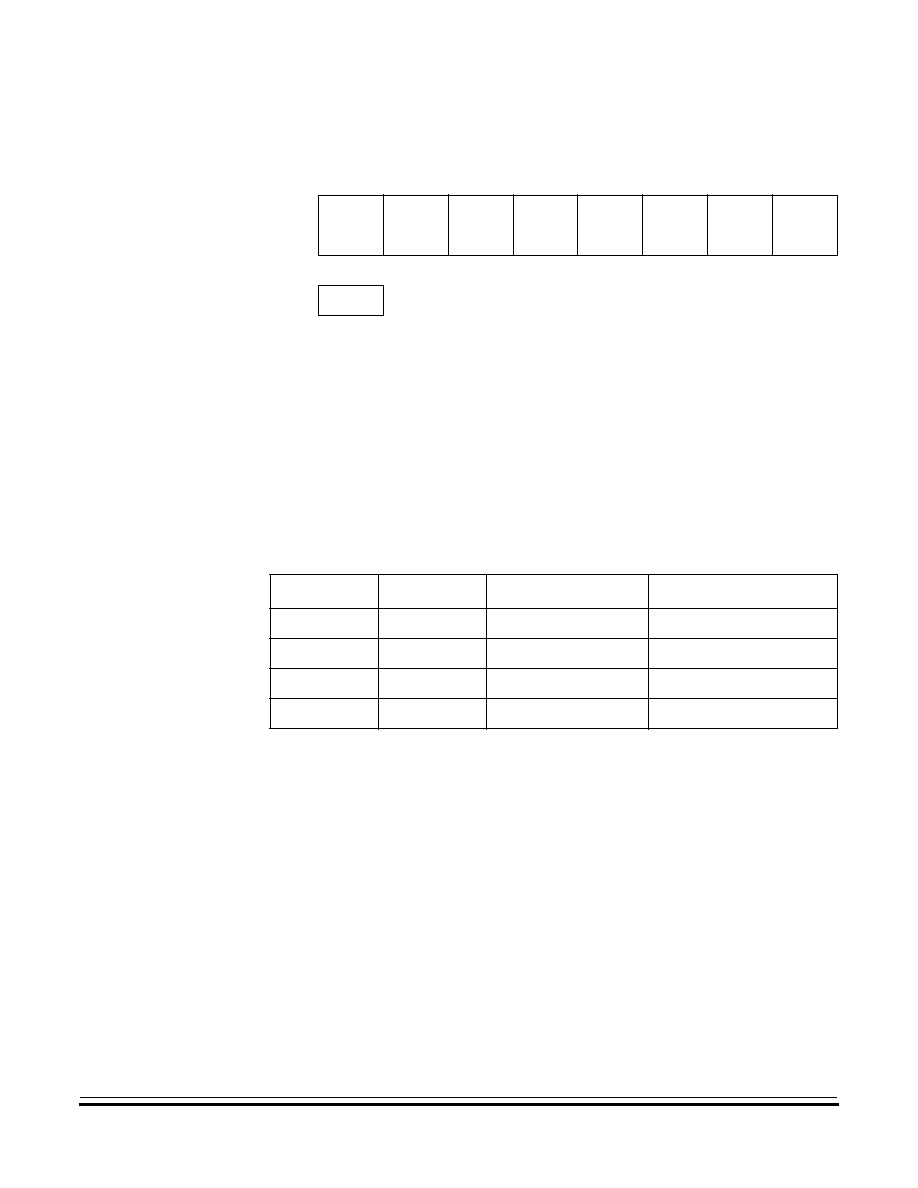
Low Voltage Inhibit (LVI)
Low-Power Modes
MC68H(R)C08JL3
--
Rev. 4
Technical Data
MOTOROLA
Low Voltage Inhibit (LVI)
171
LVID -- Low Voltage Inhibit Disable Bit
1 = Low voltage inhibit disabled
0 = Low voltage inhibit enabled
LVIT1, LVIT0 -- LVI Trip Voltage Selection
These two bits determine at which level of V
DD
the LVI module will
come into action. LVIT1 and LVIT0 are cleared by a Power-On Reset
only.
16.6 Low-Power Modes
The STOP and WAIT instructions put the MCU in low-power-
consumption standby modes.
16.6.1 Wait Mode
The LVI module, when enabled, will continue to operate in WAIT Mode.
16.6.2 Stop Mode
The LVI module, when enabled, will continue to operate in STOP Mode.
Address:
$001F
Bit 7
6
5
4
3
2
1
Bit 0
Read:
COPRS
R
R
LVID
R
SSREC
STOP
COPD
Write:
Reset:
0
0
0
0
0
0
0
0
R
= Reserved
Figure 16-3. Configuration Register 1 (CONFIG1)
LVIT1
LVIT0
Trip Voltage
(1)
1. See
Section 18. Electrical Specifications
for full parameters.
Comments
0
0
V
LVR3
(2.4V)
For V
DD
=3V operation
0
1
V
LVR3
(2.4V)
For V
DD
=3V operation
1
0
V
LVR5
(4.0V)
For V
DD
=5V operation
1
1
Reserved

Low Voltage Inhibit (LVI)
Technical Data
MC68H(R)C08JL3
--
Rev. 4
172
Low Voltage Inhibit (LVI)
MOTOROLA

MC68H(R)C08JL3
--
Rev. 4
Technical Data
MOTOROLA
Break Module (BREAK)
173
Technical Data -- MC68H(R)C08JL3
Section 17. Break Module (BREAK)
17.1 Contents
17.2
Introduction . . . . . . . . . . . . . . . . . . . . . . . . . . . . . . . . . . . . . . . 173
17.3
Features . . . . . . . . . . . . . . . . . . . . . . . . . . . . . . . . . . . . . . . . . 174
17.4
Functional Description . . . . . . . . . . . . . . . . . . . . . . . . . . . . . . 174
17.4.1
Flag Protection During Break Interrupts . . . . . . . . . . . . . . . 176
17.4.2
CPU During Break Interrupts . . . . . . . . . . . . . . . . . . . . . . . 176
17.4.3
TIM During Break Interrupts . . . . . . . . . . . . . . . . . . . . . . . . 176
17.4.4
COP During Break Interrupts . . . . . . . . . . . . . . . . . . . . . . . 176
17.5
Break Module Registers . . . . . . . . . . . . . . . . . . . . . . . . . . . . . 176
17.5.1
Break Status and Control Register (BRKSCR) . . . . . . . . . 177
17.5.2
Break Address Registers . . . . . . . . . . . . . . . . . . . . . . . . . . 178
17.5.3
Break Status Register . . . . . . . . . . . . . . . . . . . . . . . . . . . . 178
17.5.4
Break Flag Control Register (BFCR) . . . . . . . . . . . . . . . . . 180
17.6
Low-Power Modes . . . . . . . . . . . . . . . . . . . . . . . . . . . . . . . . . 180
17.6.1
Wait Mode . . . . . . . . . . . . . . . . . . . . . . . . . . . . . . . . . . . . . 180
17.6.2
Stop Mode . . . . . . . . . . . . . . . . . . . . . . . . . . . . . . . . . . . . . 180
17.2 Introduction
This section describes the break module. The break module can
generate a break interrupt that stops normal program flow at a defined
address to enter a background program.

Break Module (BREAK)
Technical Data
MC68H(R)C08JL3
--
Rev. 4
174
Break Module (BREAK)
MOTOROLA
17.3 Features
Features of the break module include the following:
∑
Accessible I/O registers during the break Interrupt
∑
CPU-generated break interrupts
∑
Software-generated break interrupts
∑
COP disabling during break interrupts
17.4 Functional Description
When the internal address bus matches the value written in the break
address registers, the break module issues a breakpoint signal (BKPT)
to the SIM. The SIM then causes the CPU to load the instruction register
with a software interrupt instruction (SWI) after completion of the current
CPU instruction. The program counter vectors to $FFFC and $FFFD
($FEFC and $FEFD in monitor mode).
The following events can cause a break interrupt to occur:
∑
A CPU-generated address (the address in the program counter)
matches the contents of the break address registers.
∑
Software writes a logic one to the BRKA bit in the break status and
control register.
When a CPU generated address matches the contents of the break
address registers, the break interrupt begins after the CPU completes its
current instruction. A return from interrupt instruction (RTI) in the break
routine ends the break interrupt and returns the MCU to normal
operation.
Figure 17-1
shows the structure of the break module.

Break Module (BREAK)
Functional Description
MC68H(R)C08JL3
--
Rev. 4
Technical Data
MOTOROLA
Break Module (BREAK)
175
Figure 17-1. Break Module Block Diagram
IAB[15:8]
IAB[7:0]
8-BIT COMPARATOR
8-BIT COMPARATOR
CONTROL
BREAK ADDRESS REGISTER LOW
BREAK ADDRESS REGISTER HIGH
IAB[15:0]
BKPT
(TO SIM)
Addr.
Register Name
Bit 7
6
5
4
3
2
1
Bit 0
$FE00
Break Status Register
(BSR)
Read:
R
R
R
R
R
R
SBSW
R
Write:
See note
Reset:
0
$FE03
Break Flag Control
Register
(BFCR)
Read:
BCFE
R
R
R
R
R
R
R
Write:
Reset:
0
$FE0C
Break Address High
Register
(BRKH)
Read:
Bit15
Bit14
Bit13
Bit12
Bit11
Bit10
Bit9
Bit8
Write:
Reset:
0
0
0
0
0
0
0
0
$FE0D
Break Address low
Register
(BRKL)
Read:
Bit7
Bit6
Bit5
Bit4
Bit3
Bit2
Bit1
Bit0
Write:
Reset:
0
0
0
0
0
0
0
0
$FE0E
Break Status and Control
Register
(BRKSCR)
Read:
BRKE
BRKA
0
0
0
0
0
0
Write:
Reset:
0
0
0
0
0
0
0
0
Note: Writing a logic 0 clears SBSW.
= Unimplemented
R
= Reserved
Figure 17-2. Break I/O Register Summary

Break Module (BREAK)
Technical Data
MC68H(R)C08JL3
--
Rev. 4
176
Break Module (BREAK)
MOTOROLA
17.4.1 Flag Protection During Break Interrupts
The system integration module (SIM) controls whether or not module
status bits can be cleared during the break state. The BCFE bit in the
break flag control register (BFCR) enables software to clear status bits
during the break state. (See
7.8.3 Break Flag Control Register (BFCR)
and see the Break Interrupts subsection for each module.)
17.4.2 CPU During Break Interrupts
The CPU starts a break interrupt by:
∑
Loading the instruction register with the SWI instruction
∑
Loading the program counter with $FFFC:$FFFD ($FEFC:$FEFD
in monitor mode)
The break interrupt begins after completion of the CPU instruction in
progress. If the break address register match occurs on the last cycle of
a CPU instruction, the break interrupt begins immediately.
17.4.3 TIM During Break Interrupts
A break interrupt stops the timer counter.
17.4.4 COP During Break Interrupts
The COP is disabled during a break interrupt when V
DD
+ V
HI
is present
on the RST pin.
17.5 Break Module Registers
These registers control and monitor operation of the break module:
∑
Break status and control register (BRKSCR)
∑
Break address register high (BRKH)
∑
Break address register low (BRKL)
∑
Break status register (BSR)
∑
Break flag control register (BFCR)

Break Module (BREAK)
Break Module Registers
MC68H(R)C08JL3
--
Rev. 4
Technical Data
MOTOROLA
Break Module (BREAK)
177
17.5.1 Break Status and Control Register (BRKSCR)
The break status and control register contains break module enable and
status bits.
BRKE -- Break Enable Bit
This read/write bit enables breaks on break address register matches.
Clear BRKE by writing a logic zero to bit 7. Reset clears the BRKE bit.
1 = Breaks enabled on 16-bit address match
0 = Breaks disabled
BRKA -- Break Active Bit
This read/write status and control bit is set when a break address
match occurs. Writing a logic one to BRKA generates a break
interrupt. Clear BRKA by writing a logic zero to it before exiting the
break routine. Reset clears the BRKA bit.
1 = Break address match
0 = No break address match
Address:
$FE0E
Bit 7
6
5
4
3
2
1
Bit 0
Read:
BRKE
BRKA
0
0
0
0
0
0
Write:
Reset:
0
0
0
0
0
0
0
0
= Unimplemented
Figure 17-3. Break Status and Control Register (BRKSCR)
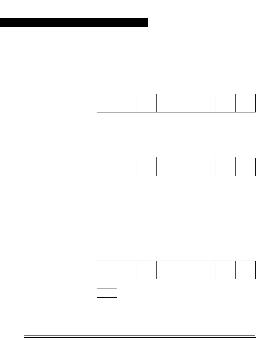
Break Module (BREAK)
Technical Data
MC68H(R)C08JL3
--
Rev. 4
178
Break Module (BREAK)
MOTOROLA
17.5.2 Break Address Registers
The break address registers contain the high and low bytes of the
desired breakpoint address. Reset clears the break address registers.
17.5.3 Break Status Register
The break status register contains a flag to indicate that a break caused
an exit from stop or wait mode.
Address:
$FE0C
Bit 7
6
5
4
3
2
1
Bit 0
Read:
Bit 15
14
13
12
11
10
9
Bit 8
Write:
Reset:
0
0
0
0
0
0
0
0
Figure 17-4. Break Address Register High (BRKH)
Address:
$FE0D
Bit 7
6
5
4
3
2
1
Bit 0
Read:
Bit 7
6
5
4
3
2
1
Bit 0
Write:
Reset:
0
0
0
0
0
0
0
0
Figure 17-5. Break Address Register Low (BRKL)
Address:
$FE00
Bit 7
6
5
4
3
2
1
Bit 0
Read:
R
R
R
R
R
R
SBSW
R
Write:
Note
(1)
Reset:
0
R
= Reserved
1. Writing a logic zero clears SBSW.
Figure 17-6. Break Status Register (BSR)

Break Module (BREAK)
Break Module Registers
MC68H(R)C08JL3
--
Rev. 4
Technical Data
MOTOROLA
Break Module (BREAK)
179
SBSW -- SIM Break Stop/Wait
This status bit is useful in applications requiring a return to wait or stop
mode after exiting from a break interrupt. Clear SBSW by writing a
logic zero to it. Reset clears SBSW.
1 = Stop mode or wait mode was exited by break interrupt
0 = Stop mode or wait mode was not exited by break interrupt
SBSW can be read within the break state SWI routine. The user can
modify the return address on the stack by subtracting one from it. The
following code is an example of this. Writing zero to the SBSW bit clears
it.
;
;
;
This code works if the H register has been pushed onto the stack in the break
service routine software. This code should be executed at the end of the
break service routine software.
HIBYTE
EQU
5
LOBYTE
EQU
6
;
If not SBSW, do RTI
BRCLR
SBSW,BSR, RETURN
;
;
See if wait mode or stop mode was exited
by break.
TST
LOBYTE,SP
; If RETURNLO is not zero,
BNE
DOLO
; then just decrement low byte.
DEC
HIBYTE,SP
; Else deal with high byte, too.
DOLO
DEC
LOBYTE,SP
; Point to WAIT/STOP opcode.
RETURN
PULH
RTI
; Restore H register.

Break Module (BREAK)
Technical Data
MC68H(R)C08JL3
--
Rev. 4
180
Break Module (BREAK)
MOTOROLA
17.5.4 Break Flag Control Register (BFCR)
The break control register contains a bit that enables software to clear
status bits while the MCU is in a break state.
BCFE -- Break Clear Flag Enable Bit
This read/write bit enables software to clear status bits by accessing
status registers while the MCU is in a break state. To clear status bits
during the break state, the BCFE bit must be set.
1 = Status bits clearable during break
0 = Status bits not clearable during break
17.6 Low-Power Modes
The WAIT and STOP instructions put the MCU in low-power-
consumption standby modes.
17.6.1 Wait Mode
If enabled, the break module is active in wait mode. In the break routine,
the user can subtract one from the return address on the stack if SBSW
is set (see
7.7 Low-Power Modes
). Clear the SBSW bit by writing logic
zero to it.
17.6.2 Stop Mode
A break interrupt causes exit from stop mode and sets the SBSW bit in
the break status register. See
7.8 SIM Registers
.
Address:
$FE03
Bit 7
6
5
4
3
2
1
Bit 0
Read:
BCFE
R
R
R
R
R
R
R
Write:
Reset:
0
R
= Reserved
Figure 17-7. Break Flag Control Register (BFCR)

MC68H(R)C08JL3
--
Rev. 4
Technical Data
MOTOROLA
Electrical Specifications
181
Technical Data -- MC68H(R)C08JL3
Section 18. Electrical Specifications
18.1 Contents
18.2
Introduction . . . . . . . . . . . . . . . . . . . . . . . . . . . . . . . . . . . . . . . 181
18.3
Absolute Maximum Ratings . . . . . . . . . . . . . . . . . . . . . . . . . . 182
18.4
Functional Operating Range. . . . . . . . . . . . . . . . . . . . . . . . . . 183
18.5
Thermal Characteristics . . . . . . . . . . . . . . . . . . . . . . . . . . . . . 183
18.6
5V DC Electrical Characteristics. . . . . . . . . . . . . . . . . . . . . . . 184
18.7
5V Control Timing . . . . . . . . . . . . . . . . . . . . . . . . . . . . . . . . . . 185
18.8
5V Oscillator Characteristics. . . . . . . . . . . . . . . . . . . . . . . . . . 186
18.9
3V DC Electrical Characteristics. . . . . . . . . . . . . . . . . . . . . . . 187
18.10 3V Control Timing . . . . . . . . . . . . . . . . . . . . . . . . . . . . . . . . . . 188
18.11 3V Oscillator Characteristics. . . . . . . . . . . . . . . . . . . . . . . . . . 189
18.12 Typical Supply Currents . . . . . . . . . . . . . . . . . . . . . . . . . . . . . 190
18.13 ADC Characteristics . . . . . . . . . . . . . . . . . . . . . . . . . . . . . . . . 191
18.2 Introduction
This section contains electrical and timing specifications.
Electrical Specifications
Technical Data
MC68H(R)C08JL3
--
Rev. 4
182
Electrical Specifications
MOTOROLA
18.3 Absolute Maximum Ratings
Maximum ratings are the extreme limits to which the MCU can be
exposed without permanently damaging it.
NOTE:
This device is not guaranteed to operate properly at the maximum
ratings. Refer to Sections
18.6
and
18.9
for guaranteed operating
conditions.
NOTE:
This device contains circuitry to protect the inputs against damage due
to high static voltages or electric fields; however, it is advised that normal
precautions be taken to avoid application of any voltage higher than
maximum-rated voltages to this high-impedance circuit. For proper
operation, it is recommended that V
IN
and V
OUT
be constrained to the
range V
SS
(V
IN
or V
OUT
)
V
DD
. Reliability of operation is enhanced if
unused inputs are connected to an appropriate logic voltage level (for
example, either V
SS
or V
DD
.)
Table 18-1. Absolute Maximum Ratings
(1)
Characteristic
Symbol
Value
Unit
Supply voltage
V
DD
≠0.3 to +6.0
V
Input voltage
V
IN
V
SS
≠0.3 to V
DD
+0.3
V
Mode entry voltage, IRQ1 pin
V
DD
+V
HI
V
SS
≠0.3 to +8.5
V
Maximum current per pin
excluding V
DD
and V
SS
I
±
25
mA
Storage temperature
T
STG
≠55 to +150
∞
C
Maximum current out of V
SS
I
MVSS
100
mA
Maximum current into V
DD
I
MVDD
100
mA
NOTE:
1. Voltages referenced to V
SS
.
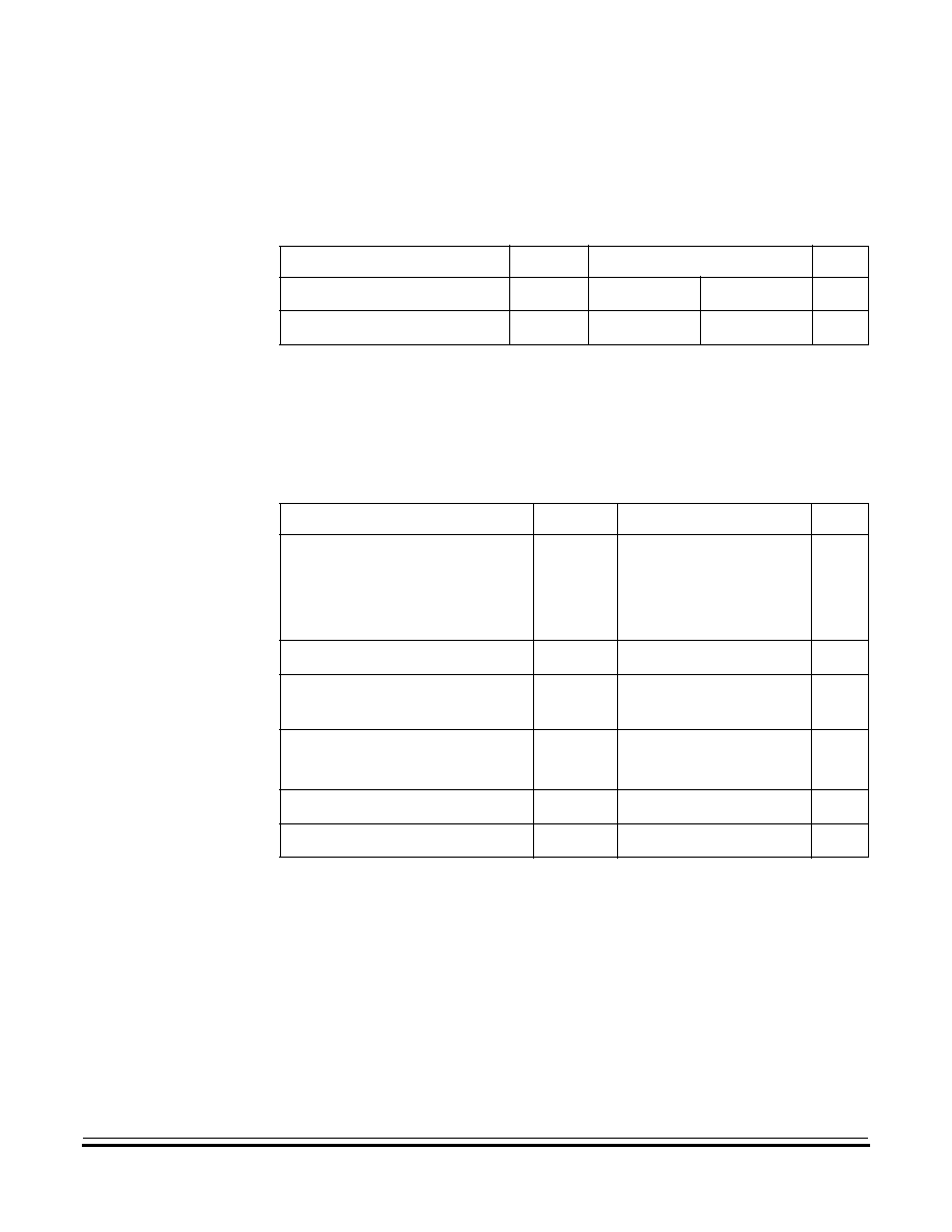
Electrical Specifications
Functional Operating Range
MC68H(R)C08JL3
--
Rev. 4
Technical Data
MOTOROLA
Electrical Specifications
183
18.4 Functional Operating Range
18.5 Thermal Characteristics
Table 18-2. Operating Range
Characteristic
Symbol
Value
Unit
Operating temperature range
T
A
≠ 40 to +125
≠ 40 to +85
∞
C
Operating voltage range
V
DD
5V
± 1
0%
3V
±
10%
V
Table 18-3. Thermal Characteristics
Characteristic
Symbol
Value
Unit
Thermal resistance
20-Pin PDIP
20-Pin SOIC
28-Pin PDIP
28-Pin SOIC
JA
70
70
70
70
∞
C/W
∞
C/W
∞
C/W
∞
C/W
I/O pin power dissipation
P
I/O
User determined
W
Power dissipation
(1)
P
D
P
D
= (I
DD
◊
V
DD
) + P
I/O
=
K/(T
J
+ 273
∞
C)
W
Constant
(2)
K
P
D
x
(T
A
+ 273
∞
C)
+ P
D
2
◊
JA
W/
∞
C
Average junction temperature
T
J
T
A
+ (P
D
◊
JA
)
∞
C
Maximum junction temperature
T
JM
100
∞
C
NOTES:
1. Power dissipation is a function of temperature.
2. K constant unique to the device. K can be determined for a known T
A
and measured
P
D.
With this value of K, P
D
and T
J
can be determined for any value of T
A
.
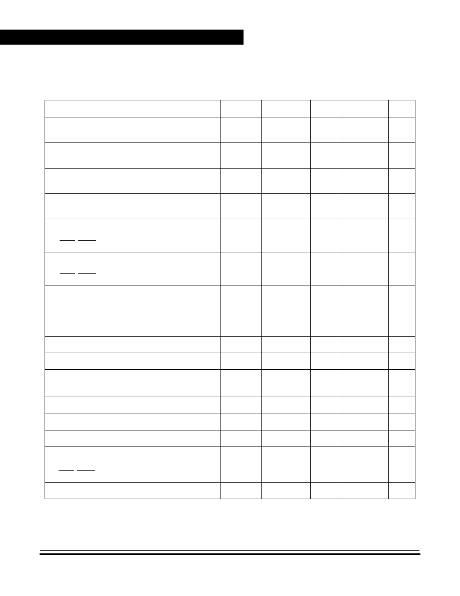
Electrical Specifications
Technical Data
MC68H(R)C08JL3
--
Rev. 4
184
Electrical Specifications
MOTOROLA
18.6 5V DC Electrical Characteristics
Table 18-4. DC Electrical Characteristics (5V)
Characteristic
(1)
Symbol
Min
Typ
(2)
Max
Unit
Output high voltage (I
LOAD
= ≠2.0mA)
PTA0≠PTA6, PTB0≠PTB7, PTD0≠PTD7
V
OH
V
DD
≠0.8
--
--
V
Output low voltage (I
LOAD
= 1.6mA)
PTA6, PTB0≠PTB7, PTD0, PTD1, PTD4, PTD5
V
OL
--
--
0.4
V
Output low voltage (I
LOAD
= 25mA)
PTD6, PTD7
V
OL
--
--
0.5
V
LED drives (V
OL
= 3V)
PTA0≠PTA5, PTD2, PTD3, PTD6, PTD7
I
OL
10
19
25
mA
Input high voltage
PTA0≠PTA6, PTB0≠PTB7, PTD0≠PTD7,
RST, IRQ1, OSC1
V
IH
0.7
◊
V
DD
--
V
DD
V
Input low voltage
PTA0≠PTA6, PTB0≠PTB7, PTD0≠PTD7,
RST, IRQ1, OSC1
V
IL
V
SS
--
0.3
◊
V
DD
V
V
DD
supply current
Run, f
OP
= 4MHz
(3)
Wait (MC68HRC08xxx)
(4)
Wait (MC68HC08xxx)
(4)
Stop
(5)
≠40
∞
C to 85
∞
C
I
DD
--
--
--
--
10
1
5
1
12
1.5
5.5
5
mA
mA
mA
µ
A
Digital I/O ports Hi-Z leakage current
I
IL
--
--
±
10
µ
A
Input current
I
IN
--
--
±
1
µ
A
Capacitance
Ports (as input or output)
C
OUT
C
IN
--
--
--
--
12
8
pF
POR rearm voltage
(6)
V
POR
0
--
100
mV
POR rise time ramp rate
(7)
R
POR
0.035
--
--
V/ms
Monitor mode entry voltage
V
DD
+V
HI
1.5
◊
V
DD
--
8.5
V
Pullup resistors
(8)
PTD6, PTD7
RST, IRQ1, PTA0≠PTA6
R
PU1
R
PU2
1.8
16
3.3
26
4.8
36
k
k
LVI reset voltage
V
LVR5
3.6
4.0
4.4
V
Electrical Specifications
5V Control Timing
MC68H(R)C08JL3
--
Rev. 4
Technical Data
MOTOROLA
Electrical Specifications
185
18.7 5V Control Timing
NOTES:
1. V
DD
= 4.5 to 5.5 Vdc, V
SS
= 0 Vdc, T
A
= T
L
to T
H
, unless otherwise noted.
2. Typical values reflect average measurements at midpoint of voltage range, 25
∞
C only.
3. Run (operating) I
DD
measured using external square wave clock source. All inputs 0.2 V from rail. No dc loads. Less
than 100 pF on all outputs. C
L
= 20 pF on OSC2. All ports configured as inputs. OSC2 capacitance linearly affects
run I
DD
. Measured with all modules enabled.
4. Wait I
DD
measured using external square wave clock source (f
OP
= 4MHz); all inputs 0.2 V from rail; no dc loads;
less than 100 pF on all outputs. C
L
= 20 pF on OSC2; all ports configured as inputs; OSC2 capacitance linearly af-
fects wait I
DD
.
5. STOP I
DD
measured with OSC1 grounded, no port pins sourcing current. LVI is disabled.
6. Maximum is highest voltage that POR is guaranteed.
7. If minimum V
DD
is not reached before the internal POR reset is released,
RST
must be driven low externally until
minimum V
DD
is reached.
8. R
PU1
and
R
PU2
are measured at
V
DD
= 5.0V
Table 18-5. Control Timing (5V)
Characteristic
(1)
NOTES:
1. V
DD
= 4.5 to 5.5 Vdc, V
SS
= 0 Vdc, T
A
= T
L
to T
H
; timing shown with respect to 20% V
DD
and 70% V
SS
, unless otherwise
noted.
Symbol
Min
Max
Unit
Internal operating frequency
(2)
2. Some modules may require a minimum frequency greater than dc for proper operation; see appropriate table for this in-
formation.
f
OP
--
8
MHz
RST input pulse width low
(3)
3. Minimum pulse width reset is guaranteed to be recognized. It is possible for a smaller pulse width to cause a reset.
t
IRL
750
--
ns
Table 18-4. DC Electrical Characteristics (5V)
Characteristic
(1)
Symbol
Min
Typ
(2)
Max
Unit
Electrical Specifications
Technical Data
MC68H(R)C08JL3
--
Rev. 4
186
Electrical Specifications
MOTOROLA
18.8 5V Oscillator Characteristics
Figure 18-1. RC vs. Frequency (5V @25
∞
C)
Table 18-6. Oscillator Component Specifications (5V)
Characteristic
Symbol
Min
Typ
Max
Unit
Crystal frequency, XTALCLK
f
OSCXCLK
--
10
32
MHz
RC oscillator frequency, RCCLK
f
RCCLK
2
10
12
MHz
External clock
reference frequency
(1)
f
OSCXCLK
dc
--
32
MHz
Crystal load capacitance
(2)
C
L
--
--
--
Crystal fixed capacitance
(2)
C
1
--
2
◊
C
L
--
Crystal tuning capacitance
(2)
C
2
--
2
◊
C
L
--
Feedback bias resistor
R
B
--
10 M
--
Series resistor
(2), (3)
R
S
--
--
--
RC oscillator external R
R
EXT
See
Figure 18-1
RC oscillator external C
C
EXT
--
10
--
pF
NOTES:
1. No more than 10% duty cycle deviation from 50%
2. Consult crystal vendor data sheet
3. Not Required for high frequency crystals
0
0
10
20
30
40
50
14
12
10
8
6
4
2
Resistor, R
EXT
(k
)
RC frequency
, f
RCCLK
(MHz)
C
EXT
= 10 pF
5V @ 25
∞
C
R
EXT
C
EXT
OSC1
V
DD
MCU
Electrical Specifications
3V DC Electrical Characteristics
MC68H(R)C08JL3
--
Rev. 4
Technical Data
MOTOROLA
Electrical Specifications
187
18.9 3V DC Electrical Characteristics
Table 18-7. DC Electrical Characteristics (3V)
Characteristic
(1)
Symbol
Min
Typ
(2)
Max
Unit
Output high voltage (I
LOAD
= ≠1.0mA)
PTA0≠PTA6, PTB0≠PTB7, PTD0≠PTD7
V
OH
V
DD
≠ 0.4
--
--
V
Output low voltage (I
LOAD
= 0.8mA)
PTA6, PTB0≠PTB7, PTD0, PTD1, PTD4, PTD5
V
OL
--
--
0.4
V
Output low voltage (I
LOAD
= 20mA)
PTD6, PTD7
V
OL
--
--
0.5
V
LED drives (V
OL
= 1.8V)
PTA0≠PTA5, PTD2, PTD3, PTD6, PTD7
I
OL
4
9
12
mA
Input high voltage
PTA0≠PTA6, PTB0≠PTB7, PTD0≠PTD7,
RST, IRQ1, OSC1
V
IH
0.7
◊
V
DD
--
V
DD
V
Input low voltage
PTA0≠PTA6, PTB0≠PTB7, PTD0≠PTD7,
RST, IRQ1, OSC1
V
IL
V
SS
--
0.3
◊
V
DD
V
V
DD
supply current
Run, f
OP
= 2MHz
(3)
Wait (MC68HRC08xxx)
(4)
Wait (MC68HC08xxx)
(4)
Stop
(5)
≠40
∞
C to 85
∞
C
I
DD
--
--
--
--
5
1
4
1
8
1.3
4.5
5
mA
mA
mA
µ
A
Digital I/O ports Hi-Z leakage current
I
IL
--
--
±
10
µ
A
Input current
I
IN
--
--
±
1
µ
A
Capacitance
Ports (as input or output)
C
OUT
C
IN
--
--
--
--
12
8
pF
POR rearm voltage
(6)
V
POR
0
--
100
mV
POR rise time ramp rate
(7)
R
POR
0.035
--
--
V/ms
Monitor mode entry voltage
V
DD
+V
HI
1.5
◊
V
DD
--
8.5
V
Pullup resistors
(8)
PTD6, PTD7
RST, IRQ1, PTA0≠PTA6
R
PU1
R
PU2
1.8
16
3.3
26
4.8
36
k
k
LVI reset voltage
V
LVR3
2.0
2.4
2.69
V
Electrical Specifications
Technical Data
MC68H(R)C08JL3
--
Rev. 4
188
Electrical Specifications
MOTOROLA
18.10 3V Control Timing
NOTES:
1. V
DD
= 2.7 to 3.3 Vdc, V
SS
= 0 Vdc, T
A
= T
L
to T
H
, unless otherwise noted.
2. Typical values reflect average measurements at midpoint of voltage range, 25
∞
C only.
3. Run (operating) I
DD
measured using external square wave clock source. All inputs 0.2 V from rail. No dc loads. Less
than 100 pF on all outputs. C
L
= 20 pF on OSC2. All ports configured as inputs. OSC2 capacitance linearly affects
run I
DD
. Measured with all modules enabled.
4. Wait I
DD
measured using external square wave clock source (f
OP
= 4MHz); all inputs 0.2 V from rail; no dc loads;
less than 100 pF on all outputs. C
L
= 20 pF on OSC2; all ports configured as inputs; OSC2 capacitance linearly af-
fects wait I
DD
.
5. STOP I
DD
measured with OSC1 grounded, no port pins sourcing current. LVI is disabled.
6. Maximum is highest voltage that POR is guaranteed.
7. If minimum V
DD
is not reached before the internal POR reset is released,
RST
must be driven low externally until
minimum V
DD
is reached.
8. R
PU1
and
R
PU2
are measured at
V
DD
= 5.0V
Table 18-8. Control Timing (3V)
Characteristic
(1)
NOTES:
1. V
DD
= 2.7 to 3.3 Vdc, V
SS
= 0 Vdc, T
A
= T
L
to T
H
; timing shown with respect to 20% V
DD
and 70% V
DD
, unless otherwise
noted.
Symbol
Min
Max
Unit
Internal operating frequency
(2)
2. Some modules may require a minimum frequency greater than dc for proper operation; see appropriate table for this in-
formation.
f
OP
--
4
MHz
RST input pulse width low
(3)
3. Minimum pulse width reset is guaranteed to be recognized. It is possible for a smaller pulse width to cause a reset.
t
IRL
1.5
--
µ
s
Table 18-7. DC Electrical Characteristics (3V)
Characteristic
(1)
Symbol
Min
Typ
(2)
Max
Unit

Electrical Specifications
3V Oscillator Characteristics
MC68H(R)C08JL3
--
Rev. 4
Technical Data
MOTOROLA
Electrical Specifications
189
18.11 3V Oscillator Characteristics
Figure 18-2. RC vs. Frequency (3V @25
∞
C)
Table 18-9. Oscillator Component Specifications (3V)
Characteristic
Symbol
Min
Typ
Max
Unit
Crystal frequency, XTALCLK
f
OSCXCLK
--
8
16
MHz
RC oscillator frequency, RCCLK
f
RCCLK
2
8
12
MHz
External clock
reference frequency
(1)
f
OSCXCLK
dc
--
16
MHz
Crystal load capacitance
(2)
C
L
--
--
--
Crystal fixed capacitance
(2)
C
1
--
2
◊
C
L
--
Crystal tuning capacitance
(2)
C
2
--
2
◊
C
L
--
Feedback bias resistor
R
B
--
10 M
--
Series resistor
(2), (3)
R
S
--
--
--
RC oscillator external R
R
EXT
See
Figure 18-2
RC oscillator external C
C
EXT
--
10
--
pF
NOTES:
1. No more than 10% duty cycle deviation from 50%
2. Consult crystal vendor data sheet
3. Not Required for high frequency crystals
0
0
10
20
30
40
50
14
12
10
8
6
4
2
Resistor, R
EXT
(k
)
RC frequency
, f
RCCLK
(MHz)
C
EXT
= 10 pF
3V @ 25
∞
C
R
EXT
C
EXT
OSC1
V
DD
MCU

Electrical Specifications
Technical Data
MC68H(R)C08JL3
--
Rev. 4
190
Electrical Specifications
MOTOROLA
18.12 Typical Supply Currents
Figure 18-3. Typical Operating I
DD
, with all Modules Turned On (25
∞
C)
Figure 18-4. Typical Wait Mode I
DD
, with ADC Turned On (25
∞
C)
Figure 18-5. Typical Stop Mode I
DD
, with all Modules Disabled (25
∞
C)
0
2
4
6
8
10
12
0
1
2
3
4
5
6
7
8
9
5.5 V
3.3 V
f
OP
or f
BUS
(MHz)
I
DD
(mA)
14
MC68HRC08xxx
0
0.25
0.5
0.75
1
1.25
1.50
1.75
2
0
1
2
3
4
5
6
7
8
5.5 V
3.3 V
I
DD
(mA)
f
OP
or f
BUS
(MHz)
MC68HRC08xxx
0
0.1
0.2
0.3
0.4
0.5
0
1
2
3
4
5
6
7
8
9
5.5 V
3.3 V
f
OP
or f
BUS
(MHz)
I
DD
(
µ
A)
MC68HRC08xxx
Electrical Specifications
ADC Characteristics
MC68H(R)C08JL3
--
Rev. 4
Technical Data
MOTOROLA
Electrical Specifications
191
18.13 ADC Characteristics
Table 18-10. ADC Characteristics
Characteristic
Symbol
Min
Max
Unit
Comments
Supply voltage
V
DDAD
2.7
(V
DD
min)
5.5
(V
DD
max)
V
Input voltages
V
ADIN
V
SS
V
DD
V
Resolution
B
AD
8
8
Bits
Absolute accuracy
A
AD
±
0.5
±
1.5
LSB
Includes quantization
ADC internal clock
f
ADIC
0.5
1.048
MHz
t
AIC
= 1/f
ADIC
, tested
only at 1 MHz
Conversion range
R
AD
V
SS
V
DD
V
Power-up time
t
ADPU
16
t
AIC
cycles
Conversion time
t
ADC
16
17
t
AIC
cycles
Sample time
(1)
NOTES:
1. Source impedances greater than 10 k
adversely affect internal RC charging time during input sampling.
t
ADS
5
--
t
AIC
cycles
Zero input reading
(2)
2. Zero-input/full-scale reading requires sufficient decoupling measures for accurate conversions.
Z
ADI
00
01
Hex
V
IN
= V
SS
Full-scale reading
(3)
F
ADI
FE
FF
Hex
V
IN
= V
DD
Input capacitance
C
ADI
--
(20) 8
pF
Not tested
Input leakage
(3)
Port B/port D
3. The external system error caused by input leakage current is approximately equal to the product of R source and input
current.
--
--
±
1
µ
A

Electrical Specifications
Technical Data
MC68H(R)C08JL3
--
Rev. 4
192
Electrical Specifications
MOTOROLA

MC68H(R)C08JL3
--
Rev. 4
Technical Data
MOTOROLA
Mechanical Specifications
193
Technical Data -- MC68H(R)C08JL3
Section 19. Mechanical Specifications
19.1 Contents
19.2
Introduction . . . . . . . . . . . . . . . . . . . . . . . . . . . . . . . . . . . . . . . 193
19.3
20-Pin PDIP . . . . . . . . . . . . . . . . . . . . . . . . . . . . . . . . . . . . . . 194
19.4
20-Pin SOIC . . . . . . . . . . . . . . . . . . . . . . . . . . . . . . . . . . . . . . 194
19.5
28-Pin PDIP . . . . . . . . . . . . . . . . . . . . . . . . . . . . . . . . . . . . . . 195
19.6
28-Pin SOIC . . . . . . . . . . . . . . . . . . . . . . . . . . . . . . . . . . . . . . 195
19.2 Introduction
This section gives the dimensions for:
∑
20-pin plastic dual in-line package (case #738)
∑
20-pin small outline integrated circuit package (case #751D)
∑
28-pin plastic dual in-line package (case #710)
∑
28-pin small outline integrated circuit package (case #751F)
The following figures show the latest package drawings at the time of
this publication. To make sure that you have the latest package
specifications, contact one of the following:
∑
Local Motorola Sales Office
∑
Motorola Mfax
≠
Phone 602-244-6609
≠
EMAIL rmfax0@email.sps.mot.com
∑
Worldwide Web (wwweb) at http://motorola.com/sps
Follow Mfax or Worldwide Web on-line instructions to retrieve the current
mechanical specifications.

Mechanical Specifications
Technical Data
MC68H(R)C08JL3
--
Rev. 4
194
Mechanical Specifications
MOTOROLA
19.3 20-Pin PDIP
Figure 19-1. 20-Pin PDIP (Case #738)
19.4 20-Pin SOIC
Figure 19-2. 20-Pin SOIC (Case #751D)
NOTES:
1. DIMENSIONING AND TOLERANCING PER ANSI
Y14.5M, 1982.
2. CONTROLLING DIMENSION: INCH.
3. DIMENSION L TO CENTER OF LEAD WHEN
FORMED PARALLEL.
4. DIMENSION B DOES NOT INCLUDE MOLD
FLASH.
M
L
J
20 PL
M
B
M
0.25 (0.010)
T
DIM
MIN
MAX
MIN
MAX
MILLIMETERS
INCHES
A
25.66
27.17
1.010
1.070
B
6.10
6.60
0.240
0.260
C
3.81
4.57
0.150
0.180
D
0.39
0.55
0.015
0.022
G
2.54 BSC
0.100 BSC
J
0.21
0.38
0.008
0.015
K
2.80
3.55
0.110
0.140
L
7.62 BSC
0.300 BSC
M
0
15
0
15
N
0.51
1.01
0.020
0.040
_
_
_
_
E
1.27
1.77
0.050
0.070
1
11
10
20
≠A≠
SEATING
PLANE
K
N
F
G
D
20 PL
≠T≠
M
A
M
0.25 (0.010)
T
E
B
C
F
1.27 BSC
0.050 BSC
NOTES:
1. DIMENSIONING AND TOLERANCING PER
ANSI Y14.5M, 1982.
2. CONTROLLING DIMENSION: MILLIMETER.
3. DIMENSIONS A AND B DO NOT INCLUDE
MOLD PROTRUSION.
4. MAXIMUM MOLD PROTRUSION 0.150
(0.006) PER SIDE.
5. DIMENSION D DOES NOT INCLUDE
DAMBAR PROTRUSION. ALLOWABLE
DAMBAR PROTRUSION SHALL BE 0.13
(0.005) TOTAL IN EXCESS OF D DIMENSION
AT MAXIMUM MATERIAL CONDITION.
≠A≠
≠B≠
20
1
11
10
S
A
M
0.010 (0.25)
B
S
T
D
20X
M
B
M
0.010 (0.25)
P
10X
J
F
G
18X
K
C
≠T≠
SEATING
PLANE
M
R
X 45
_
DIM
MIN
MAX
MIN
MAX
INCHES
MILLIMETERS
A
12.65
12.95
0.499
0.510
B
7.40
7.60
0.292
0.299
C
2.35
2.65
0.093
0.104
D
0.35
0.49
0.014
0.019
F
0.50
0.90
0.020
0.035
G
1.27 BSC
0.050 BSC
J
0.25
0.32
0.010
0.012
K
0.10
0.25
0.004
0.009
M
0
7
0
7
P
10.05
10.55
0.395
0.415
R
0.25
0.75
0.010
0.029
_
_
_
_
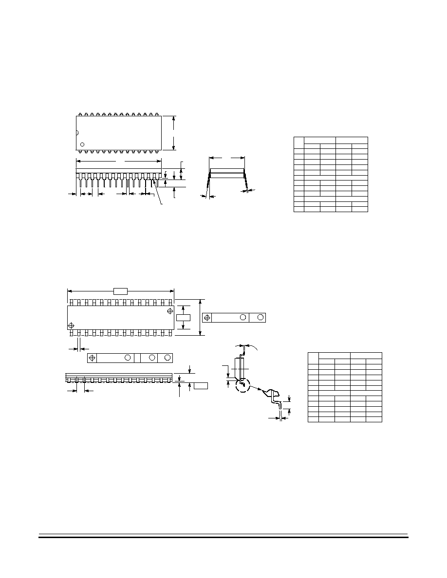
Mechanical Specifications
28-Pin PDIP
MC68H(R)C08JL3
--
Rev. 4
Technical Data
MOTOROLA
Mechanical Specifications
195
19.5 28-Pin PDIP
Figure 19-3. 28-Pin PDIP (Case #710)
19.6 28-Pin SOIC
Figure 19-4. 28-Pin SOIC (Case #751F)
NOTES:
1. POSITIONAL TOLERANCE OF LEADS (D), SHALL
BE WITHIN 0.25 (0.010) AT MAXIMUM MATERIAL
CONDITION, IN RELATION TO SEATING PLANE
AND EACH OTHER.
2. DIMENSION L TO CENTER OF LEADS WHEN
FORMED PARALLEL.
3. DIMENSION B DOES NOT INCLUDE MOLD FLASH.
1
SEATING
PLANE
15
14
28
M
A
B
K
C
N
F
G
D
H
J
L
DIM
MIN
MAX
MIN
MAX
INCHES
MILLIMETERS
A
36.45
37.21
1.435
1.465
B
13.72
14.22
0.540
0.560
C
3.94
5.08
0.155
0.200
D
0.36
0.56
0.014
0.022
F
1.02
1.52
0.040
0.060
G
2.54 BSC
0.100 BSC
H
1.65
2.16
0.065
0.085
J
0.20
0.38
0.008
0.015
K
2.92
3.43
0.115
0.135
L
15.24 BSC
0.600 BSC
M
0
∞
15
∞
0
∞
15
∞
N
0.51
1.02
0.020
0.040
NOTES:
1. DIMENSIONING AND TOLERANCING PER
ANSI Y14.5M, 1982.
2. CONTROLLING DIMENSION: MILLIMETER.
3. DIMENSION A AND B DO NOT INCLUDE
MOLD PROTRUSION.
4. MAXIMUM MOLD PROTRUSION 0.15 (0.006)
PER SIDE.
5. DIMENSION D DOES NOT INCLUDE DAMBAR
PROTRUSION. ALLOWABLE
DAMBAR PROTRUSION SHALL BE 0.13
(0.005) TOTAL IN EXCESS OF D DIMENSION
AT MAXIMUM MATERIAL CONDITION.
J
K
F
1
15
14
28
-A-
-B-
28X
14X
D
P
S
A
M
0.010 (0.25)
B
S
T
M
0.010 (0.25)
B
M
26X
G
-T-
SEATING
PLANE
C
X 45
R
M
DIM
MIN
MAX
MIN
MAX
INCHES
MILLIMETERS
A
17.80
18.05
0.701
0.711
B
7.40
7.60
0.292
0.299
C
2.35
2.65
0.093
0.104
D
0.35
0.49
0.014
0.019
F
0.41
0.90
0.016
0.035
G
1.27 BSC
0.050 BSC
J
0.23
0.32
0.009
0.013
K
0.13
0.29
0.005
0.011
M
P
10.01
10.55
0.395
0.415
R
0.25
0.75
0.010
0.029
0
∞
0
∞
8
∞
8
∞

Mechanical Specifications
Technical Data
MC68H(R)C08JL3
--
Rev. 4
196
Mechanical Specifications
MOTOROLA


Motorola reserves the right to make changes without further notice to any products herein. Motorola makes no warranty, representation or guarantee regarding the
suitability of its products for any particular purpose, nor does Motorola assume any liability arising out of the application or use of any product or circuit, and specifically
disclaims any and all liability, including without limitation consequential or incidental damages. "Typical" parameters which may be provided in Motorola data sheets and/or
specifications can and do vary in different applications and actual performance may vary over time. All operating parameters, including "Typicals" must be validated for
each customer application by customer's technical experts. Motorola does not convey any license under its patent rights nor the rights of others. Motorola products are not
designed, intended, or authorized for use as components in systems intended for surgical implant into the body, or other applications intended to support or sustain life, or
for any other application in which the failure of the Motorola product could create a situation where personal injury or death may occur. Should Buyer purchase or use
Motorola products for any such unintended or unauthorized application, Buyer shall indemnify and hold Motorola and its officers, employees, subsidiaries, affiliates, and
distributors harmless against all claims, costs, damages, and expenses, and reasonable attorney fees arising out of, directly or indirectly, any claim of personal injury or
death associated with such unintended or unauthorized use, even if such claim alleges that Motorola was negligent regarding the design or manufacture of the part.
Motorola and
are registered trademarks of Motorola, Inc. Motorola, Inc. is an Equal Opportunity/Affirmative Action Employer.
How to reach us:
USA/EUROPE/Locations Not Listed: Motorola Literature Distribution; P.O. Box 5405, Denver, Colorado 80217. 1-800-441-2447 or 1-303-675-2140
JAPAN: Nippon Motorola Ltd. SPD, Strategic Planning Office 4-32-1, Nishi-Gotanda, Shinagawa-ku, Tokyo 141, Japan. 03-5487-8488
Mfax
TM
, Motorola Fax Back System: RMFAX0@email.sps.mot.com; http://sps.motorola.com/mfax/; TOUCHTONE 1-602-244-6609;
US and Canada ONLY 1-800-774-1848
HOME PAGE: http://motorola.com/sps/
Mfax is a trademark of Motorola, Inc.
© Motorola, Inc., 2000