
This document contains detailed information on power considerations, DC/AC electrical
characteristics, and AC timing specifications for the MPC866/859 family (refer to Table 1 for
a list of devices). The MPC866P is the superset device of the MPC866/859 family.
This document describes pertinent electrical and physical characteristics of the MPC8245. For
functional characteristics of the processor, refer to the
MPC866 PowerQUICC Family Users
Manual
(MPC866UM/D).
This document contains the following topics:
Topic
Page
Section 1, "Overview"
1
Section 2, "Features"
2
Section 3, "Maximum Tolerated Ratings"
7
Section 4, "Thermal Characteristics"
9
Section 5, "Power Dissipation"
10
Section 6, "DC Characteristics"
10
Section 7, "Thermal Calculation and Measurement"
11
Section 8, "Power Supply and Power Sequencing"
14
Section 9, "Layout Practices"
15
Section 10, "Bus Signal Timing"
15
Section 11, "IEEE 1149.1 Electrical Specifications"
44
Section 12, "CPM Electrical Characteristics"
46
Section 13, "UTOPIA AC Electrical Specifications"
70
Section 14, "FEC Electrical Characteristics"
72
Section 15, "Mechanical Data and Ordering Information"
75
Section 16, "Document Revision History"
88
1
Overview
The MPC866/859 is a derivative of Motorola's MPC860 PowerQUICCTM family of devices.
It is a versatile single-chip integrated microprocessor and peripheral combination that can be
used in a variety of controller applications and communications and networking systems. The
MPC866/859/859DSL provides enhanced ATM functionality over that of other ATM-enabled
members of the MPC860 family.
Advance Information
MPC866EC/D
Rev. 1.4, 8/2003
MPC866/859
Hardware Specifications
2
MPC866/859 Hardware Specifications
MOTOROLA
Features
Features
Table 1 shows the functionality supported by the members of the MPC866/859 family.
2
Features
The following list summarizes the key MPC866/859 features:
∑
Embedded single-issue, 32-bit PowerPCTM core (implementing the PowerPC architecture) with
thirty-two 32-bit general-purpose registers (GPRs)
-- The core performs branch prediction with conditional prefetch, without conditional execution
-- 4- or 8-Kbyte data cache and 4- or 16-Kbyte instruction cache (see Table 1)
≠ 16-Kbyte instruction cache (MPC866P and MPC859P) is four-way, set-associative with 256
sets; 4-Kbyte instruction cache (MPC866T, MPC859T, and MPC859DSL) is two-way,
set-associative with 128 sets.
≠ 8-Kbyte data cache (MPC866P and MPC859P) is two-way, set-associative with 256 sets;
4-Kbyte data cache(MPC866T, MPC859T, and MPC859DSL) is two-way, set-associative
with 128 sets.
≠ Cache coherency for both instruction and data caches is maintained on 128-bit (4-word)
cache blocks
≠ Caches are physically addressed, implement a least recently used (LRU) replacement
algorithm, and are lockable on a cache block basis.
-- MMUs with 32-entry TLB, fully associative instruction and data TLBs
-- MMUs support multiple page sizes of 4, 16, and 512 Kbytes, and 8 Mbytes; 16 virtual address
spaces and 16 protection groups.
-- Advanced on-chip-emulation debug mode
∑
The MPC866/859 provides enhanced ATM functionality over that of the MPC860SAR. The
MPC866/859 adds major new features available in 'enhanced SAR' (ESAR) mode, including the
following:
-- Improved operation, administration, and maintenance (OAM) support
-- OAM performance monitoring (PM) support
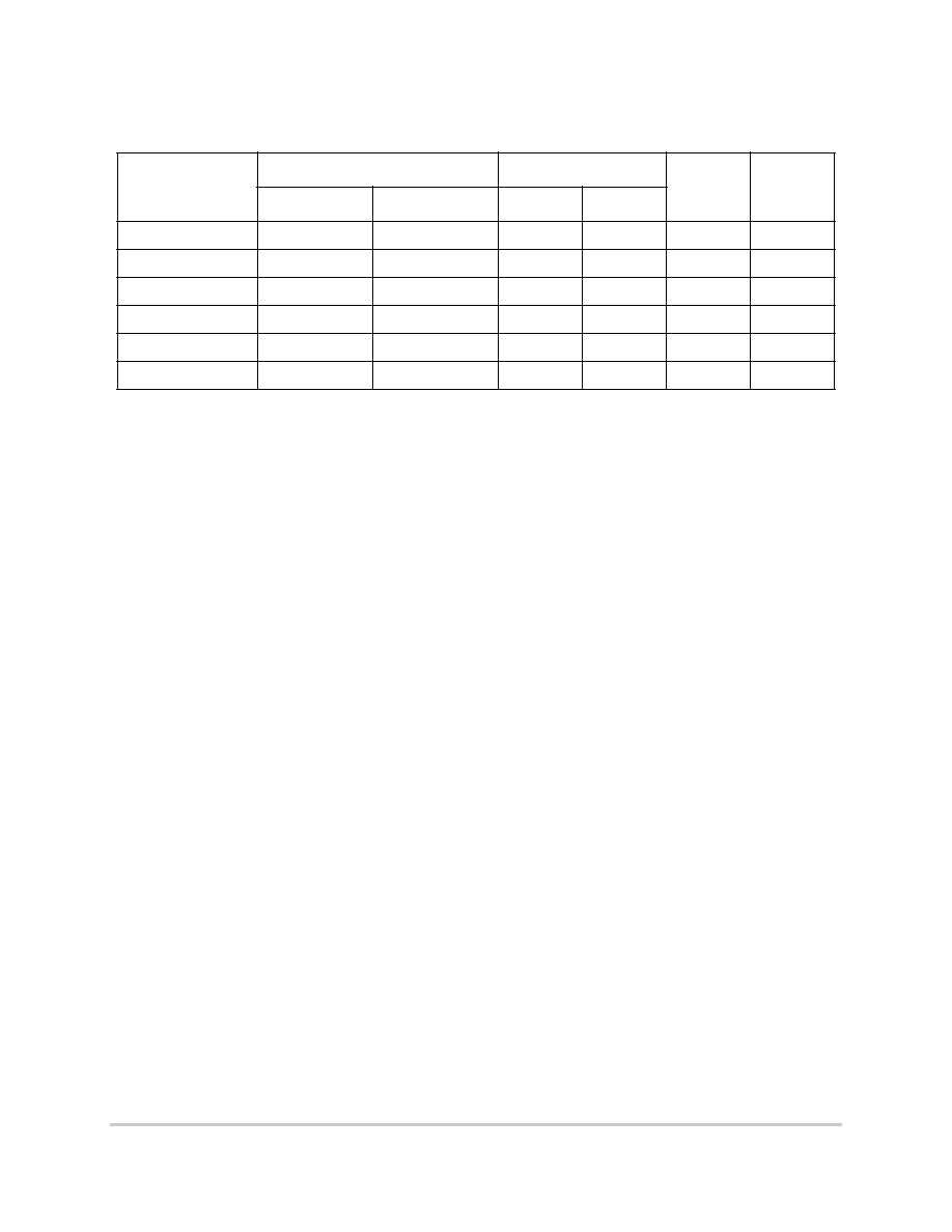
Table 1. MPC866 Family Functionality
Part
Cache
Ethernet
SCC SMC
Instruction Data 10T
10/100
MPC866P
16 Kbytes
8 Kbytes
Up to 4
1
4
2
MPC866T
4 Kbytes
4 Kbytes
Up to 4
1
4
2
MPC859P
16 Kbytes
8 Kbytes
1
1
1
2
MPC859T
4 Kbytes
4 Kbytes
1
1
1
2
MPC859DSL
4 Kbytes
4 Kbytes
1
1
1
1
1
On the MPC859DSL, the SCC (SCC1) is for ethernet only. Also, the MPC859DSL does not support the Time Slot
Assigner (TSA).
1
2
2
On the MPC859DSL, the SMC (SMC1) is for UART only.
MPC852T
3
3
For more details on the MPC852T, please refer to the
MPC852T Hardware Specifications.
4 KBytes
4 Kbytes
2
1
2
1

MOTOROLA
MPC866/859 Hardware Specifications
3
Features
-- Multiple APC priority levels available to support a range of traffic pace requirements
-- ATM port-to-port switching capability without the need for RAM-based microcode
-- Simultaneous MII (10/100Base-T) and UTOPIA (half-duplex) capability
-- Optional statistical cell counters per PHY
-- UTOPIA level 2 compliant interface with added FIFO buffering to reduce the total cell
transmission time. (The earlier UTOPIA level 1 specification is also supported.)
≠ Multi-PHY support on the MPC866, MPC859P, and MPC859T
≠ Four PHY support on the MPC866/859
-- Parameter RAM for both SPI and I
2
C can be relocated without RAM-based microcode
-- Supports full-duplex UTOPIA both master (ATM side) and slave (PHY side) operation using a
'split' bus
-- AAL2/VBR functionality is ROM-resident.
∑
Up to 32-bit data bus (dynamic bus sizing for 8, 16, and 32 bits)
∑
Thirty-two address lines
∑
Memory controller (eight banks)
-- Contains complete dynamic RAM (DRAM) controller
-- Each bank can be a chip select or RAS to support a DRAM bank
-- Up to 30 wait states programmable per memory bank
-- Glueless interface to page mode/EDO/SDRAM, SRAM, EPROMs, flash EPROMs, and other
memory devices.
-- DRAM controller programmable to support most size and speed memory interfaces
-- Four CAS lines, four WE lines, and one OE line
-- Boot chip-select available at reset (options for 8-, 16-, or 32-bit memory)
-- Variable block sizes (32 Kbytes≠256 Mbytes)
-- Selectable write protection
-- On-chip bus arbitration logic
∑
General-purpose timers
-- Four 16-bit timers cascadable to be two 32-bit timers
-- Gate mode can enable/disable counting
-- Interrupt can be masked on reference match and event capture
∑
Fast Ethernet controller (FEC)
-- Simultaneous MII (10/100Base-T) and UTOPIA operation when using the UTOPIA
multiplexed bus
∑
System integration unit (SIU)
-- Bus monitor
-- Software watchdog
-- Periodic interrupt timer (PIT)
-- Low-power stop mode
-- Clock synthesizer
-- Decrementer and time base from the PowerPC architecture
-- Reset controller

4
MPC866/859 Hardware Specifications
MOTOROLA
Features
Features
-- IEEE 1149.1 test access port (JTAG)
∑
Interrupts
-- Seven external interrupt request (IRQ) lines
-- Twelve port pins with interrupt capability
-- The MPC866P and MPC866T have 23 internal interrupt sources; the MPC859P, MPC859T,
and MPC859DSL have 20 internal interrupt sources.
-- Programmable priority between SCCs (MPC866P and MPC866T)
-- Programmable highest priority request
∑
Communications processor module (CPM)
-- RISC controller
-- Communication-specific commands (for example,
GRACEFUL
STOP
TRANSMIT
,
ENTER
HUNT
MODE
, and
RESTART
TRANSMIT
)
-- Supports continuous mode transmission and reception on all serial channels
-- Up to 8-Kbytes of dual-port RAM
-- MPC866P and MPC866T have 16 serial DMA (SDMA) channels; MPC859P, MPC859T, and
MPC859DSL have 10 serial DMA (SDMA) channels.
-- Three parallel I/O registers with open-drain capability
∑
Four baud rate generators
-- Independent (can be connected to any SCC or SMC)
-- Allow changes during operation
-- Autobaud support option
∑
MPC866P and MPC866T have four SCCs (serial communication controller); MPC859P,
MPC859T, and MPC859DSL have one SCC; and SCC1 on MPC859DSL supports Ethernet only.
-- Serial ATM capability on all SCCs
-- Optional UTOPIA port on SCC4
-- Ethernet/IEEE 802.3 optional on SCC1≠4, supporting full 10-Mbps operation
-- HDLC/SDLC
-- HDLC bus (implements an HDLC-based local area network (LAN))
-- Asynchronous HDLC to support PPP (point-to-point protocol)
-- AppleTalk
-- Universal asynchronous receiver transmitter (UART)
-- Synchronous UART
-- Serial infrared (IrDA)
-- Binary synchronous communication (BISYNC)
-- Totally transparent (bit streams)
-- Totally transparent (frame based with optional cyclic redundancy check (CRC)
∑
Two SMCs (serial management channels) (MPC859DSL has one SMC (SMC1) for UART.)
-- UART
-- Transparent
-- General circuit interface (GCI) controller
-- Can be connected to the time-division multiplexed (TDM) channels

MOTOROLA
MPC866/859 Hardware Specifications
5
Features
∑
One serial peripheral interface (SPI)
-- Supports master and slave modes
-- Supports multiple-master operation on the same bus
∑
One inter-integrated circuit (I
2
C) port
-- Supports master and slave modes
-- Multiple-master environment support
∑
Time slot assigner (TSA) (MPC859DSL does not have TSA.)
-- Allows SCCs and SMCs to run in multiplexed and/or non-multiplexed operation
-- Supports T1, CEPT, PCM highway, ISDN basic rate, ISDN primary rate, user-defined
-- 1- or 8-bit resolution
-- Allows independent transmit and receive routing, frame synchronization, and clocking
-- Allows dynamic changes
-- On MPC866P and MPC866T, can be internally connected to six serial channels (four SCCs and
two SMCs); on MPC859P and MPC859T, can be connected to three serial channels (one SCC
and two SMCs).
∑
Parallel interface port (PIP)
-- Centronics interface support
-- Supports fast connection between compatible ports on MPC866/859 or MC68360
∑
PCMCIA interface
-- Master (socket) interface, compliant with PCI Local Bus Specification (Rev 2.1)
-- Supports one or two PCMCIA sockets whether ESAR functionality is enabled
-- Eight memory or I/O windows supported
∑
Debug interface
-- Eight comparators: four operate on instruction address, two operate on data address, and two
operate on data.
-- Supports conditions: =
< >
-- Each watchpoint can generate a breakpoint internally
∑
Normal high and normal low power modes to conserve power
∑
1.8 V core and 3.3 V I/O operation with 5-V TTL compatibility; refer to Table 6 for a listing of the
5-V tolerant pins.
∑
357-pin plastic ball grid array (PBGA) package
∑
Operation up to 133 MHz
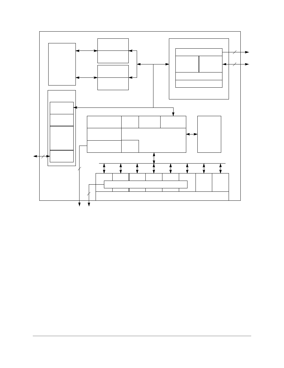
The MPC866/859 is comprised of three modules that each use a 32-bit internal bus: MPC8xx core, system
integration unit (SIU), and communication processor module (CPM). The MPC866P block diagram is
shown in Figure 1 on page 6. The MPC859P/859T/859DSL block diagram is shown in Figure 2 on page 7.
6
MPC866/859 Hardware Specifications
MOTOROLA
Features
Features
Figure 1. MPC866P Block Diagram
SCC3
SCC4
Bus
System Interface Unit (SIU)
Embedded
Parallel I/O
Memory Controller
4
Timers
Interrupt
Controllers
8-Kbyte
Dual-Port RAM
16 Virtual
Serial
and
2
Independent
DMA
Channels
System Functions
PCMCIA/ATA Interface
16-Kbyte
Instruction Cache
32-Entry ITLB
Instruction MMU
8-Kbyte
Data Cache
32-Entry DTLB
Data MMU
Instruction
Bus
Load/Store
Bus
Unified
4 Baud Rate
Generators
Parallel Interface Port
and UTOPIA
Internal
Bus Interface
Unit
External
Bus Interface
Unit
Timers
32-Bit RISC Controller
and Program
ROM
SCC1
Serial Interface
I
2
C
SPI
SMC2
SMC1
SCC2
Time Slot Assigner
MPC8xx
Processor
Core
DMAs
FIFOs
10/100
MII
Base-T
Media Access
Time Slot Assigner
Control
Fast Ethernet
Controller
MOTOROLA
MPC866/859 Hardware Specifications
7
Maximum Tolerated Ratings
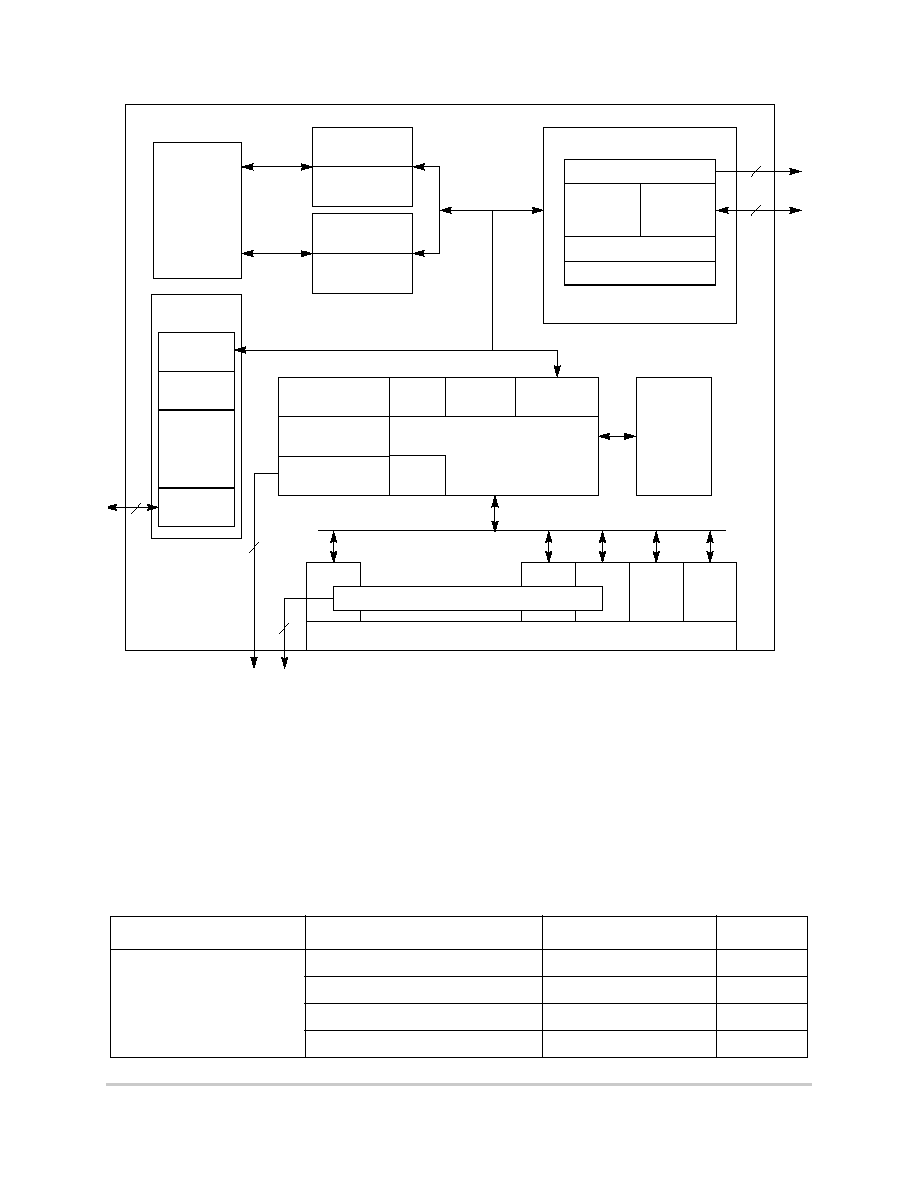
Figure 2. MPC859P/859T/MPC859DSL Block Diagram
3
Maximum Tolerated Ratings
This section provides the maximum tolerated voltage and temperature ranges for the MPC866/859. Table 2
shows the maximum tolerated ratings, and Table 3 shows the operating temperatures.
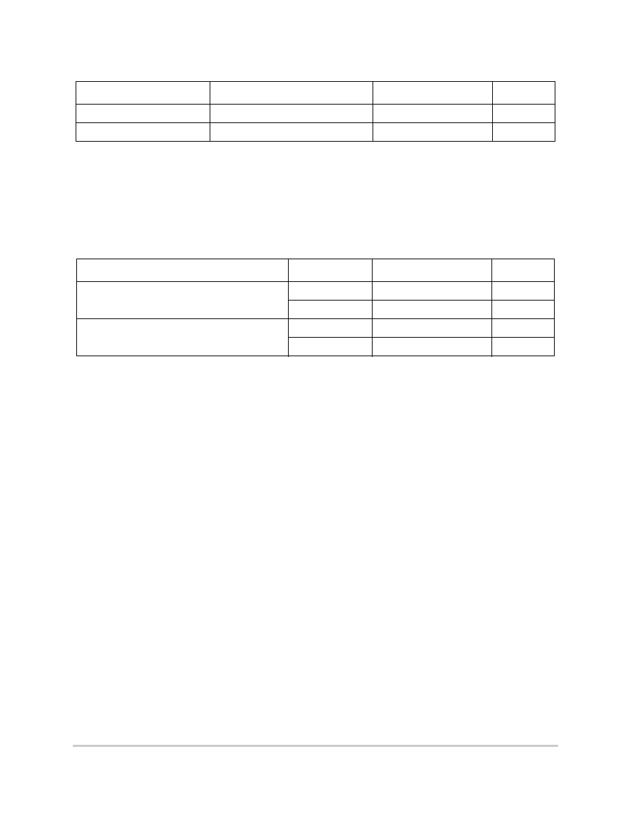
Table 2. Maximum Tolerated Ratings
Rating
Symbol
Value
Unit
Supply voltage
1
VDDH
≠ 0.3 to 4.0
V
VDDL
≠ 0.3 to 2.0
V
VDDSYN
≠ 0.3 to 2.0
V
Difference between VDDL to VDDSYN
100
mV
Bus
System Interface Unit (SIU)
Embedded
Parallel I/O
Memory Controller
4
Timers
Interrupt
Controllers
8-Kbyte
Dual-Port RAM
10 Virtual
Serial
and
2
Independent
DMA
Channels
System Functions
PCMCIA/ATA Interface
4-Kbyte
Instruction Cache
32-Entry ITLB
Instruction MMU
4-Kbyte
Data Cache
32-Entry DTLB
Data MMU
Instruction
Bus
Load/Store
Bus
Unified
4 Baud Rate
Generators
Parallel Interface Port
and UTOPIA
Internal
Bus Interface
Unit
External
Bus Interface
Unit
Timers
32-Bit RISC Controller
and Program
ROM
SCC1
Serial Interface
I
2
C
SPI
SMC2*
SMC1
Time Slot Assigner
MPC8xx
Processor
Core
DMAs
FIFOs
10/100
MII
Base-T
Media Access
Time Slot Assigner*
Control
Fast Ethernet
Controller
* The MPC859DSL does not contain SMC2 nor the time slot assigner, and provides eight SDMA
controllers.
The MPC859P has a 16-Kbyte instruction cache and a 8-Kbyte data cache.
8
MPC866/859 Hardware Specifications
MOTOROLA
Maximum Tolerated Ratings
Maximum Tolerated Ratings
Table 3. Operating Temperatures
This device contains circuitry protecting against damage due to high-static voltage or electrical fields;
however, it is advised that normal precautions be taken to avoid application of any voltages higher than
maximum-rated voltages to this high-impedance circuit. Reliability of operation is enhanced if unused
inputs are tied to an appropriate logic voltage level (for example, either GND or V
DD
).
Input voltage
2
V
in
GND ≠ 0.3 to VDDH
V
Storage temperature range
T
stg
≠55 to +150
∞C
1
The power supply of the device must start its ramp from 0.0 V.
2
Functional operating conditions are provided with the DC electrical specifications in Table 6. Absolute maximum
ratings are stress ratings only; functional operation at the maxima is not guaranteed. Stress beyond those listed may
affect device reliability or cause permanent damage to the device. See page 14.
Caution
: All inputs that tolerate 5 V cannot be more than 2.5 V greater than VDDH. This restriction applies to
power-up and normal operation (that is, if the MPC866/859 is unpowered, a voltage greater than 2.5 V must not be
applied to its inputs).
Rating
Symbol
Value
Unit
Temperature
1
(standard)
1
Minimum temperatures are guaranteed as ambient temperature, T
A
. Maximum temperatures are guaranteed as
junction temperature, T
j
.
T
A(min)
0
∞C
T
j(max)
95
∞C
Temperature (extended)
T
A(min)
≠40
∞C
T
j(max)
100
∞C
Table 2. Maximum Tolerated Ratings (continued)
Rating
Symbol
Value
Unit

MOTOROLA
MPC866/859 Hardware Specifications
9
Thermal Characteristics
4
Thermal Characteristics
Table 4 shows the thermal characteristics for the MPC866/859.
Table 4. MPC866/859 Thermal Resistance Data
Rating
Environment
Symbol
Value
Unit
Junction-to-ambient
1
1
Junction temperature is a function of on-chip power dissipation, package thermal resistance, mounting site (board)
temperature, ambient temperature, airflow, power dissipation of other components on the board, and board thermal
resistance.
Natural Convection
Single-layer board (1s)
R
JA
2
2
Per SEMI G38-87 and JEDEC JESD51-2 with the single-layer board horizontal.
37
∞C/W
Four-layer board (2s2p)
R
JMA
3
3
Per JEDEC JESD51-6 with the board horizontal.
23
Airflow (200 ft/min)
Single-layer board (1s)
R
JMA
3
30
Four-layer board (2s2p)
R
JMA
3
19
Junction-to-board
4
4
Thermal resistance between the die and the printed-circuit board per JEDEC JESD51-8. Board temperature is
measured on the top surface of the board near the package.
R
JB
13
Junction-to-case
5
5
Indicates the average thermal resistance between the die and the case top surface as measured by the cold plate
method (MIL SPEC-883 Method 1012.1) with the cold plate temperature used for the case temperature. For exposed
pad packages where the pad would be expected to be soldered, junction-to-case thermal resistance is a simulated
value from the junction to the exposed pad without contact resistance.
R
JC
6
Junction-to-package top
6
6
Thermal characterization parameter indicating the temperature difference between package top and junction
temperature per JEDEC JESD51-2.
Natural Convection
JT
2
Airflow (200 ft/min)
JT
2
10
MPC866/859 Hardware Specifications
MOTOROLA
Power Dissipation
Power Dissipation
5
Power Dissipation
Table 5 shows power dissipation information. The modes are 1:1, where CPU and bus speeds are equal, and
2:1 mode, where CPU frequency is twice the bus speed.
6
DC Characteristics
Table 6 shows the DC electrical characteristics for the MPC866/859.
Table 5. Power Dissipation (P
D
)
Die Revision
Bus Mode
CPU
Frequency
Typical
1
1
Typical power dissipation at VDDL and VDDSYN is at 1.8 V. and VDDH is at 3.3 V.
Maximum
2
2
Maximum power dissipation at VDDL and VDDSYN is at 1.9 V, and VDDH is at 3.465 V.
NOTE
Values in Table 5 represent VDDL based power dissipation and
do not include I/O power dissipation over VDDH. I/O power
dissipation varies widely by application due to buffer current,
depending on external circuitry. The VDDSYN power
dissipation is negligible.
Unit
0
1:1 50
MHz
110
140
mW
66 MHz
150
180
mW
2:1
66 MHz
140
160
mW
80 MHz
170
200
mW
100 MHz
210
250
mW
133 MHz
260
320
mW
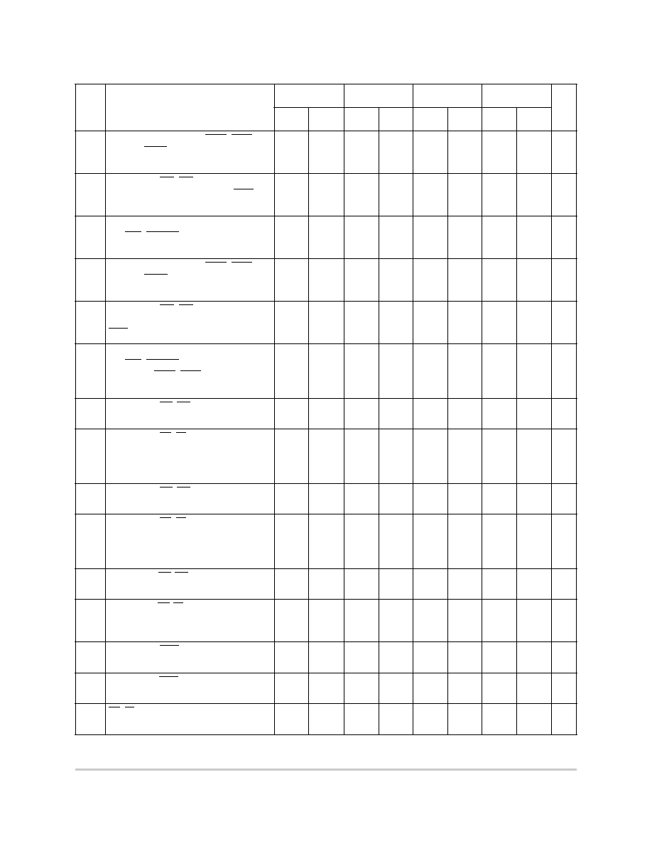
Table 6. DC Electrical Specifications
Characteristic
Symbol
Min
Max
Unit
Operating voltage
VDDL (core)
1.7
1.9
V
VDDH (I/O)
3.135
3.465
V
VDDSYN
1
1.7
1.9
V
Difference between
VDDL to VDDSYN
--
100
mV
Input high voltage (all inputs except EXTAL and
EXTCLK)
2
VIH
2.0
3.465
V
MOTOROLA
MPC866/859 Hardware Specifications
11
Thermal Calculation and Measurement
7
Thermal Calculation and Measurement
For the following discussions, P
D
= (VDDL x IDDL) + PI/O, where PI/O is the power dissipation of the I/O
drivers. The VDDSYN power dissipation is negligible.
Input low voltage
VIL
GND
0.8
V
EXTAL, EXTCLK input high voltage
VIHC
0.7*(VDDH)
VDDH
V
Input leakage current, Vin = 5.5V (except TMS, TRST,
DSCK and DSDI pins) for 5 Volts Tolerant Pins
2
I
in
--
100
µA
Input leakage current, Vin = VDDH (except TMS, TRST,
DSCK, and DSDI)
I
In
--
10
µA
Input leakage current, Vin = 0 V (except TMS, TRST,
DSCK and DSDI pins)
I
In
--
10
µA
Input capacitance
3
C
in
--
20
pF
Output high voltage, IOH = ≠ 2.0 mA,
except XTAL, and Open drain pins
VOH
2.4
--
V
Output low voltage
∑ IOL = 2.0 mA (CLKOUT)
∑ IOL = 3.2 mA
4
∑ IOL = 5.3 mA
5
∑ IOL = 7.0 mA (TXD1/PA14, TXD2/PA12)
∑ IOL = 8.9 mA (TS, TA, TEA, BI, BB, HRESET, SRESET)
VOL
--
0.5
V
1
The difference between VDDL and VDDSYN can not be more than 100 m V.
2
The signals PA[0:15], PB[14:31], PC[4:15], PD[3:15], TDI, TDO, TCK, TRST_B, TMS, MII_TXEN, MII_MDIO are 5 V
tolerant.
3
Input capacitance is periodically sampled.
4
A(0:31), TSIZ0/REG, TSIZ1, D(0:31), DP(0:3)/IRQ(3:6), RD/WR, BURST, RSV/IRQ2, IP_B(0:1)/IWP(0:1)/VFLS(0:1),
IP_B2/IOIS16_B/AT2, IP_B3/IWP2/VF2, IP_B4/LWP0/VF0, IP_B5/LWP1/VF1, IP_B6/DSDI/AT0, IP_B7/PTR/AT3,
RXD1 /PA15, RXD2/PA13, L1TXDB/PA11, L1RXDB/PA10, L1TXDA/PA9, L1RXDA/PA8,
TIN1/L1RCLKA/BRGO1/CLK1/PA7, BRGCLK1/TOUT1/CLK2/PA6, TIN2/L1TCLKA/BRGO2/CLK3/PA5,
TOUT2/CLK4/PA4, TIN3/BRGO3/CLK5/PA3, BRGCLK2/L1RCLKB/TOUT3/CLK6/PA2, TIN4/BRGO4/CLK7/PA1,
L1TCLKB/TOUT4/CLK8/PA0, REJCT1/SPISEL/PB31, SPICLK/PB30, SPIMOSI/PB29, BRGO4/SPIMISO/PB28,
BRGO1/I2CSDA/PB27, BRGO2/I2CSCL/PB26, SMTXD1/PB25, SMRXD1/PB24, SMSYN1/SDACK1/PB23,
SMSYN2/SDACK2/PB22, SMTXD2/L1CLKOB/PB21, SMRXD2/L1CLKOA/PB20, L1ST1/RTS1/PB19,
L1ST2/RTS2/PB18, L1ST3/L1RQB/PB17, L1ST4/L1RQA/PB16, BRGO3/PB15, RSTRT1/PB14,
L1ST1/RTS1/DREQ0/PC15, L1ST2/RTS2/DREQ1/PC14, L1ST3/L1RQB/PC13, L1ST4/L1RQA/PC12, CTS1/PC11,
TGATE1/CD1/PC10, CTS2/PC9, TGATE2/CD2/PC8, CTS3/SDACK2/L1TSYNCB/PC7, CD3/L1RSYNCB/PC6,
CTS4/SDACK1/L1TSYNCA/PC5, CD4/L1RSYNCA/PC4, PD15/L1TSYNCA, PD14/L1RSYNCA, PD13/L1TSYNCB,
PD12/L1RSYNCB, PD11/RXD3, PD10/TXD3, PD9/RXD4, PD8/TXD4, PD5/REJECT2, PD6/RTS4, PD7/RTS3,
PD4/REJECT3, PD3, MII_MDC, MII_TX_ER, MII_EN, MII_MDIO, MII_TXD[0:3].
5
BDIP/GPL_B(5), BR, BG, FRZ/IRQ6, CS(0:5), CS(6)/CE(1)_B, CS(7)/CE(2)_B, WE0/BS_B0/IORD,
WE1/BS_B1/IOWR, WE2/BS_B2/PCOE, WE3/BS_B3/PCWE, BS_A(0:3), GPL_A0/GPL_B0, OE/GPL_A1/GPL_B1,
GPL_A(2:3)/GPL_B(2:3)/CS(2:3), UPWAITA/GPL_A4, UPWAITB/GPL_B4, GPL_A5, ALE_A, CE1_A, CE2_A,
ALE_B/DSCK/AT1, OP(0:1), OP2/MODCK1/STS, OP3/MODCK2/DSDO, BADDR(28:30).
Table 6. DC Electrical Specifications (continued)
Characteristic
Symbol
Min
Max
Unit

12
MPC866/859 Hardware Specifications
MOTOROLA
Thermal Calculation and Measurement
Thermal Calculation and Measurement
7.1
Estimation with Junction-to-Ambient Thermal
Resistance
An estimation of the chip junction temperature, T
J
, in ∞C can be obtained from the equation:
T
J
= T
A
+(R
JA
x P
D
)
where:
T
A
= ambient temperature (∫C)
R
JA
= package junction-to-ambient thermal resistance (∫C/W)
P
D
= power dissipation in package
The junction-to-ambient thermal resistance is an industry standard value that provides a quick and easy
estimation of thermal performance. However, the answer is only an estimate; test cases have demonstrated
that errors of a factor of two (in the quantity T
J
-T
A
) are possible.
7.2
Estimation with Junction-to-Case Thermal Resistance
Historically, the thermal resistance has frequently been expressed as the sum of a junction-to-case thermal
resistance and a case-to-ambient thermal resistance:
R
JA
= R
JC
+ R
CA
where:
R
JA
= junction-to-ambient thermal resistance (∫C/W)
R
JC
= junction-to-case thermal resistance (∫C/W)
R
CA
= case-to-ambient thermal resistance (∫C/W)
R
JC
is device related and cannot be influenced by the user. The user adjusts the thermal environment to
affect the case-to-ambient thermal resistance, R
CA
. For instance, the user can change the airflow around
the device, add a heat sink, change the mounting arrangement on the printed-circuit board, or change the
thermal dissipation on the printed-circuit board surrounding the device. This thermal model is most useful
for ceramic packages with heat sinks where some 90% of the heat flows through the case and the heat sink
to the ambient environment. For most packages, a better model is required.
7.3
Estimation with Junction-to-Board Thermal Resistance
A simple package thermal model that has demonstrated reasonable accuracy (about 20%) is a two-resistor
model consisting of a junction-to-board and a junction-to-case thermal resistance. The junction-to-case
covers the situation where a heat sink is used or where a substantial amount of heat is dissipated from the
top of the package. The junction-to-board thermal resistance describes the thermal performance when most
of the heat is conducted to the printed-circuit board. It has been observed that the thermal performance of
most plastic packages and especially PBGA packages is strongly dependent on the board temperature; see
Figure 3.

MOTOROLA
MPC866/859 Hardware Specifications
13
Thermal Calculation and Measurement
Figure 3. Effect of Board Temperature Rise on Thermal Behavior
If the board temperature is known, an estimate of the junction temperature in the environment can be made
using the following equation:
T
J
= T
B
+(R
JB
x
P
D
)
where:
R
JB
= junction-to-board thermal resistance (∫C/W)
T
B
= board temperature ∫C
P
D
= power dissipation in package
If the board temperature is known and the heat loss from the package case to the air can be ignored,
acceptable predictions of junction temperature can be made. For this method to work, the board and board
mounting must be similar to the test board used to determine the junction-to-board thermal resistance,
namely a 2s2p (board with a power and a ground plane) and vias attaching the thermal balls to the ground
plane.
7.4
Estimation Using Simulation
When the board temperature is not known, a thermal simulation of the application is needed. The simple
two-resistor model can be used with the thermal simulation of the application [2], or a more accurate and
complex model of the package can be used in the thermal simulation.
0
1 0
2 0
3 0
4 0
5 0
6 0
7 0
8 0
9 0
1 0 0
0
2 0
4 0
6 0
8 0
Board Temperture Rise Above Ambient Divided by Package
Power
Junction Temperature Rise Above
Ambient Divided by Package Power

14
MPC866/859 Hardware Specifications
MOTOROLA
Power Supply and Power Sequencing
Power Supply and Power Sequencing
7.5
Experimental Determination
To determine the junction temperature of the device in the application after prototypes are available, the
thermal characterization parameter (
JT
) can be used to determine the junction temperature with a
measurement of the temperature at the top center of the package case using the following equation:
T
J
= T
T
+(
JT
x P
D
)
where:
JT
= thermal characterization parameter
T
T
= thermocouple temperature on top of package
P
D
= power dissipation in package
The thermal characterization parameter is measured per JESD51-2 specification published by JEDEC using
a 40 gauge type T thermocouple epoxied to the top center of the package case. The thermocouple should be
positioned so that the thermocouple junction rests on the package. A small amount of epoxy is placed over
the thermocouple junction and over about 1 mm of wire extending from the junction. The thermocouple wire
is placed flat against the package case to avoid measurement errors caused by cooling effects of the
thermocouple wire.
7.6
References
Semiconductor Equipment and Materials International
(415) 964-5111
805 East Middlefield Rd.
Mountain View, CA 94043
MIL-SPEC and EIA/JESD (JEDEC) specifications
800-854-7179 or
(Available from Global Engineering Documents)
303-397-7956
JEDEC Specifications
http://www.jedec.org
1. C.E. Triplett and B. Joiner, "An Experimental Characterization of a 272 PBGA Within an Automotive
Engine Controller Module," Proceedings of SemiTherm, San Diego, 1998, pp. 47-54.
2. B. Joiner and V. Adams, "Measurement and Simulation of Junction to Board Thermal Resistance and Its
Application in Thermal Modeling," Proceedings of SemiTherm, San Diego, 1999, pp. 212-220.
8
Power Supply and Power Sequencing
This section provides design considerations for the MPC866/859 power supply. The MPC866/859 has a
core voltage (VDDL) and PLL voltage (VDDSYN) that operates at a lower voltage than the I/O voltage
VDDH. The I/O section of the MPC866/859 is supplied with 3.3 V across VDDH and V
SS
(GND).
Signals PA[0:15], PB[14:31], PC[4:15], PD[3:15], TDI, TDO, TCK, TRST_B, TMS, MII_TXEN, and
MII_MDIO are 5-V tolerant. All inputs cannot be more than 2.5 V greater than VDDH. In addition, 5-V
tolerant pins cannot exceed 5.5 V and the remaining input pins cannot exceed 3.465 V. This restriction
applies to power up/down and normal operation.
One consequence of multiple power supplies is that when power is initially applied the voltage rails ramp
up at different rates. The rates depend on the nature of the power supply, the type of load on each power
supply, and the manner in which different voltages are derived. The following restrictions apply:
∑
VDDL must not exceed VDDH during power up and power down.
∑
VDDL must not exceed 1.9 V and VDDH must not exceed 3.465 V.
MOTOROLA
MPC866/859 Hardware Specifications
15
Layout Practices
These cautions are necessary for the long term reliability of the part. If they are violated, the electrostatic
discharge (ESD) protection diodes are forward-biased and excessive current can flow through these diodes.
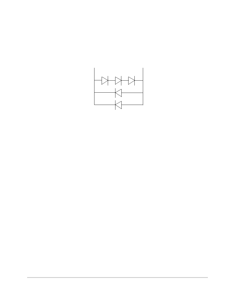
If the system power supply design does not control the voltage sequencing, the circuit shown in Figure 4
can be added to meet these requirements. The MUR420 Schottky diodes control the maximum potential
difference between the external bus and core power supplies on powerup and the 1N5820 diodes regulate
the maximum potential difference on powerdown.
Figure 4. Example Voltage Sequencing Circuit
9
Layout Practices
Each V
DD
pin on the MPC866/859 should be provided with a low-impedance path to the board's supply.
Furthermore, each GND pin should be provided with a low-impedance path to ground. The power supply
pins drive distinct groups of logic on chip. The V
DD
power supply should be bypassed to ground using at
least four 0.1 µF bypass capacitors located as close as possible to the four sides of the package. Each board
designed should be characterized and additional appropriate decoupling capacitors should be used if
required. The capacitor leads and associated printed-circuit traces connecting to chip V
DD
and GND should
be kept to less than 1/2" per capacitor lead. At a minimum, a four-layer board employing two inner layers
as V
DD
and GND planes should be used.
All output pins on the MPC866/859 have fast rise and fall times. Printed-circuit (PC) trace interconnection
length should be minimized in order to minimize undershoot and reflections caused by these fast output
switching times. This recommendation particularly applies to the address and data buses. Maximum PC
trace lengths of 6" are recommended. Capacitance calculations should consider all device loads as well as
parasitic capacitances due to the PC traces. Attention to proper PCB layout and bypassing becomes
especially critical in systems with higher capacitive loads because these loads create higher transient
currents in the V
DD
and GND circuits. Pull up all unused inputs or signals that will be inputs during reset.
Special care should be taken to minimize the noise levels on the PLL supply pins. For more information,
please refer to Section 14.4.3, Clock Synthesizer Power (VDDSYN, VSSSYN, VSSSYN1), in the MPC866
User's Manual.
10
Bus Signal Timing
The maximum bus speed supported by the MPC866/859 is 66 MHz. Higher-speed parts must be operated
in half-speed bus mode (for example, an MPC866/859 used at 100 MHz must be configured for a 50-MHz
bus). Table 7 and Table 8 show the frequency ranges for standard part frequencies.
VDDH
VDDL
1N5820
MUR420
16
MPC866/859 Hardware Specifications
MOTOROLA
Bus Signal Timing
Bus Signal Timing
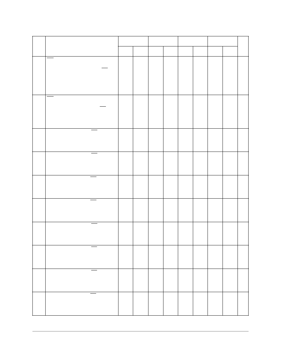
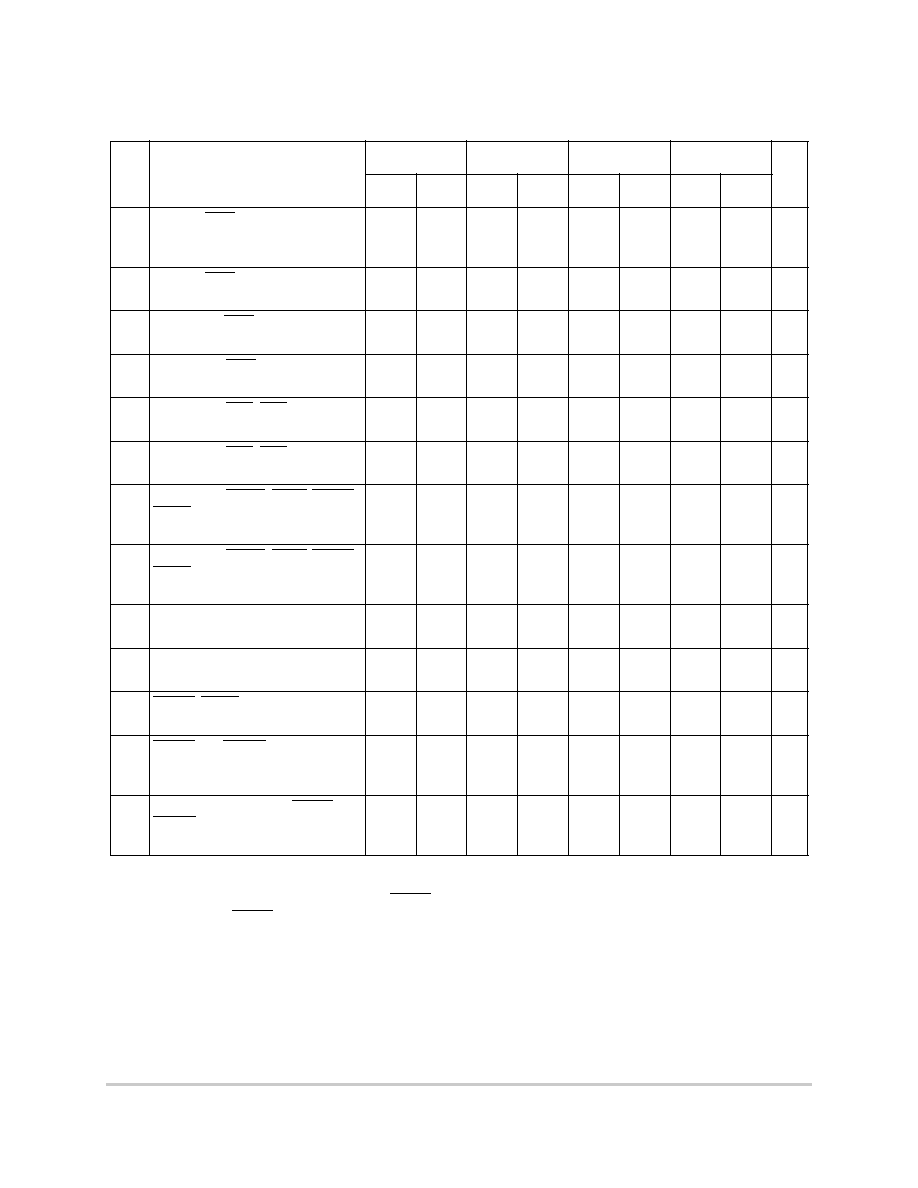
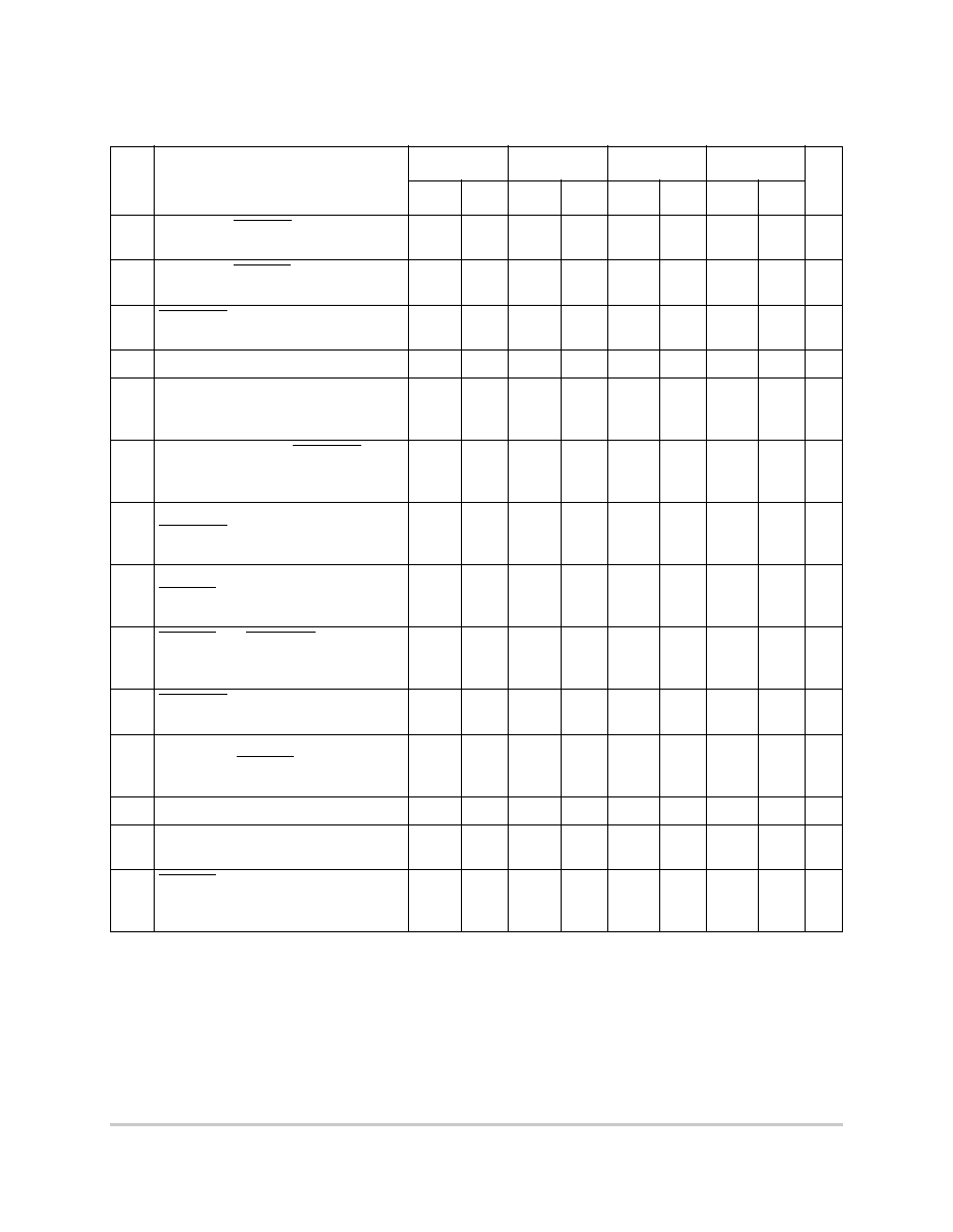
Table 9 shows the timings for the MPC866/859 at 33, 40, 50, and 66 MHz bus operation. The timing for the
MPC866/859 bus shown in this table assumes a 50-pF load for maximum delays and a 0-pF load for
minimum delays. CLKOUT assumes a 100-pF load maximum delay.
Table 7. Frequency Ranges for Standard Part Frequencies (1:1 Bus Mode)
Part Freq
50 MHz
66 MHz
Min
Max
Min
Max
Core 40
50
40
66.67
Bus 40
50
40
66.67
Table 8. Frequency Ranges for Standard Part Frequencies (2:1 Bus Mode)
Part
Freq
50 MHz
66 MHz
100 MHz
133 MHz
Min
Max
Min
Max
Min
Max
Min
Max
Core 40
50
40
66.67
40
100
40
133.34
Bus 20
25
20
33.33
20
50
20
66.67
Table 9. Bus Operation Timings
Num
Characteristic
33 MHz
40 MHz
50 MHz
66 MHz
Unit
Min
Max
Min
Max
Min
Max
Min
Max
B1
Bus Period (CLKOUT) See Table 7
--
--
--
--
--
--
--
--
ns
B1a
EXTCLK to CLKOUT phase skew
≠ 2
+2
≠ 2
+2
≠ 2
+2
≠ 2
+2
ns
B1b
CLKOUT frequency jitter peak-to-peak
--
1
--
1
--
1
--
1
ns
B1c
Frequency jitter on EXTCLK
--
0.50
--
0.50
--
0.50
--
0.50
%
B1d
CLKOUT phase jitter peak-to-peak
for OSCLK
15 MHz
--
4
--
4
--
4
--
4
ns
CLKOUT phase jitter peak-to-peak
for OSCLK < 15 MHz
--
5
--
5
--
5
--
5
ns
B2
CLKOUT pulse width low (MIN = 0.4 x
B1, MAX = 0.6 x B1)
12.1
18.2
10.0
15.0
8.0
12.0
6.1
9.1
ns
B3
CLKOUT pulse width high (MIN = 0.4 x
B1, MAX = 0.6 x B1)
12.1
18.2
10.0
15.0
8.0
12.0
6.1
9.1
ns
B4
CLKOUT rise time
--
4.00
--
4.00
--
4.00
--
4.00
ns
B5
CLKOUT fall time
--
4.00
--
4.00
--
4.00
--
4.00
ns
B7
CLKOUT to A(0:31), BADDR(28:30),
RD/WR, BURST, D(0:31), DP(0:3)
output hold (MIN = 0.25 x B1)
7.60
--
6.30
--
5.00
--
3.80
--
ns
MOTOROLA
MPC866/859 Hardware Specifications
17
Bus Signal Timing
B7a
CLKOUT to TSIZ(0:1), REG, RSV,
AT(0:3), BDIP, PTR output hold (MIN =
0.25 x B1)
7.60
--
6.30
--
5.00
--
3.80
--
ns
B7b
CLKOUT to BR, BG, FRZ, VFLS(0:1),
VF(0:2), IWP(0:2), LWP(0:1), STS
output hold (MIN = 0.25 x B1)
7.60
--
6.30
--
5.00
--
3.80
--
ns
B8
CLKOUT to A(0:31), BADDR(28:30)
RD/WR, BURST, D(0:31), DP(0:3),
valid (MAX = 0.25 x B1 + 6.3)
--
13.80
--
12.50
--
11.30
--
10.00
ns
B8a
CLKOUT to TSIZ(0:1), REG, RSV,
AT(0:3), BDIP, PTR valid (MAX = 0.25
x B1 + 6.3)
--
13.80
--
12.50
--
11.30
--
10.00
ns
B8b
CLKOUT to BR, BG, VFLS(0:1),
VF(0:2), IWP(0:2), FRZ, LWP(0:1),
STS valid
4
(MAX = 0.25 x B1 + 6.3)
--
13.80
--
12.50
--
11.30
--
10.00
ns
B9
CLKOUT to A(0:31), BADDR(28:30),
RD/WR, BURST, D(0:31), DP(0:3),
TSIZ(0:1), REG, RSV, AT(0:3), PTR
High-Z (MAX = 0.25 x B1 + 6.3)
7.60
13.80
6.30
12.50
5.00
11.30
3.80
10.00
ns
B11
CLKOUT to TS, BB assertion (MAX =
0.25 x B1 + 6.0)
7.60
13.60
6.30
12.30
5.00
11.00
3.80
9.80
ns
B11a CLKOUT to TA, BI assertion (when
driven by the memory controller or
PCMCIA interface) (MAX = 0.00 x B1 +
9.30
1
)
2.50
9.30
2.50
9.30
2.50
9.30
2.50
9.80
ns
B12
CLKOUT to TS, BB negation (MAX =
0.25 x B1 + 4.8)
7.60
12.30
6.30
11.00
5.00
9.80
3.80
8.50
ns
B12a CLKOUT to TA, BI negation (when
driven by the memory controller or
PCMCIA interface) (MAX = 0.00 x B1 +
9.00)
2.50
9.00
2.50
9.00
2.50
9.00
2.50
9.00
ns
B13
CLKOUT to TS, BB High-Z (MIN = 0.25
x B1)
7.60
21.60
6.30
20.30
5.00
19.00
3.80
14.00
ns
B13a CLKOUT to TA, BI High-Z (when driven
by the memory controller or PCMCIA
interface) (MIN = 0.00 x B1 + 2.5)
2.50
15.00
2.50
15.00
2.50
15.00
2.50
15.00
ns
B14
CLKOUT to TEA assertion (MAX =
0.00 x B1 + 9.00)
2.50
9.00
2.50
9.00
2.50
9.00
2.50
9.00
ns
B15
CLKOUT to TEA High-Z (MIN = 0.00 x
B1 + 2.50)
2.50
15.00
2.50
15.00
2.50
15.00
2.50
15.00
ns
B16
TA, BI valid to CLKOUT (setup time)
(MIN = 0.00 x B1 + 6.00)
6.00
--
6.00
--
6.00
--
6.00
--
ns
Table 9. Bus Operation Timings (continued)
Num
Characteristic
33 MHz
40 MHz
50 MHz
66 MHz
Unit
Min
Max
Min
Max
Min
Max
Min
Max
18
MPC866/859 Hardware Specifications
MOTOROLA
Bus Signal Timing
Bus Signal Timing
B16a TEA, KR, RETRY, CR valid to
CLKOUT (setup time) (MIN = 0.00 x B1
+ 4.5)
4.50
--
4.50
--
4.50
--
4.50
--
ns
B16b BB, BG, BR, valid to CLKOUT (setup
time)
2
(4 MIN = 0.00 x B1 + 0.00 )
4.00
--
4.00
--
4.00
--
4.00
--
ns
B17
CLKOUT to TA, TEA, BI, BB, BG, BR
valid (hold time) (MIN = 0.00 x B1 +
1.00
3
)
1.00
--
1.00
--
1.00
--
2.00
--
ns
B17a CLKOUT to KR, RETRY, CR valid
(hold time) (MIN = 0.00 x B1 + 2.00)
2.00
--
2.00
--
2.00
--
2.00
--
ns
B18
D(0:31), DP(0:3) valid to CLKOUT
rising edge (setup time)
4
(MIN = 0.00
x B1 + 6.00)
6.00
--
6.00
--
6.00
--
6.00
--
ns
B19
CLKOUT rising edge to D(0:31),
DP(0:3) valid (hold time)
4
(MIN = 0.00
x B1 + 1.00
5
)
1.00
--
1.00
--
1.00
--
2.00
--
ns
B20
D(0:31), DP(0:3) valid to CLKOUT
falling edge (setup time)
6
(MIN = 0.00
x B1 + 4.00)
4.00
--
4.00
--
4.00
--
4.00
--
ns
B21
CLKOUT falling edge to D(0:31),
DP(0:3) valid (hold Time)
6
(MIN = 0.00
x B1 + 2.00)
2.00
--
2.00
--
2.00
--
2.00
--
ns
B22
CLKOUT rising edge to CS asserted
GPCM ACS = 00 (MAX = 0.25 x B1 +
6.3)
7.60
13.80
6.30
12.50
5.00
11.30
3.80
10.00
ns
B22a CLKOUT falling edge to CS asserted
GPCM ACS = 10, TRLX = 0 (MAX =
0.00 x B1 + 8.00)
--
8.00
--
8.00
--
8.00
--
8.00
ns
B22b CLKOUT falling edge to CS asserted
GPCM ACS = 11, TRLX = 0, EBDF = 0
(MAX = 0.25 x B1 + 6.3)
7.60
13.80
6.30
12.50
5.00
11.30
3.80
10.00
ns
B22c CLKOUT falling edge to CS asserted
GPCM ACS = 11, TRLX = 0, EBDF = 1
(MAX = 0.375 x B1 + 6.6)
10.90
18.00
10.90
16.00
7.00
14.10
5.20
12.30
ns
B23
CLKOUT rising edge to CS negated
GPCM read access, GPCM write
access ACS = 00, TRLX = 0 & CSNT =
0 (MAX = 0.00 x B1 + 8.00)
2.00
8.00
2.00
8.00
2.00
8.00
2.00
8.00
ns
B24
A(0:31) and BADDR(28:30) to CS
asserted GPCM ACS = 10, TRLX = 0
(MIN = 0.25 x B1 - 2.00)
5.60
--
4.30
--
3.00
--
1.80
--
ns
Table 9. Bus Operation Timings (continued)
Num
Characteristic
33 MHz
40 MHz
50 MHz
66 MHz
Unit
Min
Max
Min
Max
Min
Max
Min
Max
MOTOROLA
MPC866/859 Hardware Specifications
19
Bus Signal Timing
B24a A(0:31) and BADDR(28:30) to CS
asserted GPCM ACS = 11, TRLX = 0
(MIN = 0.50 x B1 - 2.00)
13.20
--
10.50
--
8.00
--
5.60
--
ns
B25
CLKOUT rising edge to OE, WE(0:3)
asserted (MAX = 0.00 x B1 + 9.00)
--
9.00
--
9.00
--
9.00
--
9.00
ns
B26
CLKOUT rising edge to OE negated
(MAX = 0.00 x B1 + 9.00)
2.00
9.00
2.00
9.00
2.00
9.00
2.00
9.00
ns
B27
A(0:31) and BADDR(28:30) to CS
asserted GPCM ACS = 10, TRLX = 1
(MIN = 1.25 x B1 - 2.00)
35.90
--
29.30
--
23.00
--
16.90
--
ns
B27a A(0:31) and BADDR(28:30) to CS
asserted GPCM ACS = 11, TRLX = 1
(MIN = 1.50 x B1 - 2.00)
43.50
--
35.50
--
28.00
--
20.70
--
ns
B28
CLKOUT rising edge to WE(0:3)
negated GPCM write access CSNT =
0 (MAX = 0.00 x B1 + 9.00)
--
9.00
--
9.00
--
9.00
--
9.00
ns
B28a CLKOUT falling edge to WE(0:3)
negated GPCM write access TRLX =
0,1, CSNT = 1, EBDF = 0 (MAX = 0.25
x B1 + 6.80)
7.60
14.30
6.30
13.00
5.00
11.80
3.80
10.50
ns
B28b CLKOUT falling edge to CS negated
GPCM write access TRLX = 0,1,
CSNT = 1, ACS = 10 or ACS = 11,
EBDF = 0 (MAX = 0.25 x B1 + 6.80)
--
14.30
--
13.00
--
11.80
--
10.50
ns
B28c CLKOUT falling edge to WE(0:3)
negated GPCM write access TRLX =
0, CSNT = 1 write access TRLX = 0,1,
CSNT = 1, EBDF = 1 (MAX = 0.375 x
B1 + 6.6)
10.90
18.00
10.90
18.00
7.00
14.30
5.20
12.30
ns
B28d CLKOUT falling edge to CS negated
GPCM write access TRLX = 0,1,
CSNT = 1, ACS = 10, or ACS = 11,
EBDF = 1 (MAX = 0.375 x B1 + 6.6)
--
18.00
--
18.00
--
14.30
--
12.30
ns
B29
WE(0:3) negated to D(0:31), DP(0:3)
High-Z GPCM write access, CSNT = 0,
EBDF = 0 (MIN = 0.25 x B1 - 2.00)
5.60
--
4.30
--
3.00
--
1.80
--
ns
B29a WE(0:3) negated to D(0:31), DP(0:3)
High-Z GPCM write access, TRLX = 0,
CSNT = 1, EBDF = 0 (MIN = 0.50 x B1
≠ 2.00)
13.20
--
10.50
--
8.00
--
5.60
--
ns
B29b CS negated to D(0:31), DP(0:3), High
Z GPCM write access, ACS = 00,
TRLX = 0,1 & CSNT = 0 (MIN = 0.25 x
B1≠ 2.00)
5.60
--
4.30
--
3.00
--
1.80
--
ns
Table 9. Bus Operation Timings (continued)
Num
Characteristic
33 MHz
40 MHz
50 MHz
66 MHz
Unit
Min
Max
Min
Max
Min
Max
Min
Max
20
MPC866/859 Hardware Specifications
MOTOROLA
Bus Signal Timing
Bus Signal Timing
B29c CS negated to D(0:31), DP(0:3)
High-Z GPCM write access, TRLX = 0,
CSNT = 1, ACS = 10, or ACS = 11,
EBDF = 0 (MIN = 0.50 x B1 ≠ 2.00)
13.20
--
10.50
--
8.00
--
5.60
--
ns
B29d WE(0:3) negated to D(0:31), DP(0:3)
High-Z GPCM write access, TRLX = 1,
CSNT = 1, EBDF = 0 (MIN = 1.50 x B1
≠ 2.00)
43.50
--
35.50
--
28.00
--
20.70
--
ns
B29e CS negated to D(0:31), DP(0:3)
High-Z GPCM write access, TRLX = 1,
CSNT = 1, ACS = 10, or ACS = 11,
EBDF = 0 (MIN = 1.50 x B1 ≠ 2.00)
43.50
--
35.50
--
28.00
--
20.70
--
ns
B29f WE(0:3) negated to D(0:31), DP(0:3)
High Z GPCM write access, TRLX = 0,
CSNT = 1, EBDF = 1 (MIN = 0.375 x
B1 ≠ 6.30)
5.00
--
3.00
--
1.10
--
0.00
--
ns
B29g CS negated to D(0:31), DP(0:3)
High-Z GPCM write access, TRLX = 0,
CSNT = 1 ACS = 10 or ACS = 11,
EBDF = 1 (MIN = 0.375 x B1 ≠ 6.30)
5.00
--
3.00
--
1.10
--
0.00
--
ns
B29h WE(0:3) negated to D(0:31), DP(0:3)
High Z GPCM write access, TRLX = 1,
CSNT = 1, EBDF = 1 (MIN = 0.375 x
B1 ≠ 3.30)
38.40
--
31.10
--
24.20
--
17.50
--
ns
B29i CS negated to D(0:31), DP(0:3)
High-Z GPCM write access, TRLX = 1,
CSNT = 1, ACS = 10 or ACS = 11,
EBDF = 1 (MIN = 0.375 x B1 ≠ 3.30)
38.40
--
31.10
--
24.20
--
17.50
--
ns
B30
CS, WE(0:3) negated to A(0:31),
BADDR(28:30) invalid GPCM write
access
7
(MIN = 0.25 x B1 ≠ 2.00)
5.60
--
4.30
--
3.00
--
1.80
--
ns
B30a WE(0:3) negated to A(0:31),
BADDR(28:30) invalid GPCM, write
access, TRLX = 0, CSNT = 1, CS
negated to A(0:31) invalid GPCM write
access TRLX = 0, CSNT =1 ACS = 10,
or ACS == 11, EBDF = 0 (MIN = 0.50 x
B1 ≠ 2.00)
13.20
--
10.50
--
8.00
--
5.60
--
ns
B30b WE(0:3) negated to A(0:31) invalid
GPCM BADDR(28:30) invalid GPCM
write access, TRLX = 1, CSNT = 1. CS
negated to A(0:31) invalid GPCM write
access TRLX = 1, CSNT = 1, ACS =
10, or ACS == 11 EBDF = 0 (MIN =
1.50 x B1 ≠ 2.00)
43.50
--
35.50
--
28.00
--
20.70
--
ns
Table 9. Bus Operation Timings (continued)
Num
Characteristic
33 MHz
40 MHz
50 MHz
66 MHz
Unit
Min
Max
Min
Max
Min
Max
Min
Max
MOTOROLA
MPC866/859 Hardware Specifications
21
Bus Signal Timing
B30c WE(0:3) negated to A(0:31),
BADDR(28:30) invalid GPCM write
access, TRLX = 0, CSNT = 1. CS
negated to A(0:31) invalid GPCM write
access, TRLX = 0, CSNT = 1 ACS =
10, ACS == 11, EBDF = 1 (MIN = 0.375
x B1 ≠ 3.00)
8.40
--
6.40
--
4.50
--
2.70
--
ns
B30d WE(0:3) negated to A(0:31),
BADDR(28:30) invalid GPCM write
access TRLX = 1, CSNT =1, CS
negated to A(0:31) invalid GPCM write
access TRLX = 1, CSNT = 1, ACS = 10
or 11, EBDF = 1
38.67
--
31.38
--
24.50
--
17.83
--
ns
B31
CLKOUT falling edge to CS valid, as
requested by control bit CST4 in the
corresponding word in the UPM (MAX
= 0.00 X B1 + 6.00)
1.50
6.00
1.50
6.00
1.50
6.00
1.50
6.00
ns
B31a CLKOUT falling edge to CS valid, as
requested by control bit CST1 in the
corresponding word in the UPM (MAX
= 0.25 x B1 + 6.80)
7.60
14.30
6.30
13.00
5.00
11.80
3.80
10.50
ns
B31b CLKOUT rising edge to CS valid, as
requested by control bit CST2 in the
corresponding word in the UPM (MAX
= 0.00 x B1 + 8.00)
1.50
8.00
1.50
8.00
1.50
8.00
1.50
8.00
ns
B31c CLKOUT rising edge to CS valid, as
requested by control bit CST3 in the
corresponding word in the UPM (MAX
= 0.25 x B1 + 6.30)
7.60
13.80
6.30
12.50
5.00
11.30
3.80
10.00
ns
B31d CLKOUT falling edge to CS valid, as
requested by control bit CST1 in the
corresponding word in the UPM EBDF
= 1 (MAX = 0.375 x B1 + 6.6)
13.30
18.00
11.30
16.00
9.40
14.10
7.60
12.30
ns
B32
CLKOUT falling edge to BS valid, as
requested by control bit BST4 in the
corresponding word in the UPM (MAX
= 0.00 x B1 + 6.00)
1.50
6.00
1.50
6.00
1.50
6.00
1.50
6.00
ns
B32a CLKOUT falling edge to BS valid, as
requested by control bit BST1 in the
corresponding word in the UPM, EBDF
= 0 (MAX = 0.25 x B1 + 6.80)
7.60
14.30
6.30
13.00
5.00
11.80
3.80
10.50
ns
B32b CLKOUT rising edge to BS valid, as
requested by control bit BST2 in the
corresponding word in the UPM (MAX
= 0.00 x B1 + 8.00)
1.50
8.00
1.50
8.00
1.50
8.00
1.50
8.00
ns
Table 9. Bus Operation Timings (continued)
Num
Characteristic
33 MHz
40 MHz
50 MHz
66 MHz
Unit
Min
Max
Min
Max
Min
Max
Min
Max

22
MPC866/859 Hardware Specifications
MOTOROLA
Bus Signal Timing
Bus Signal Timing
B32c CLKOUT rising edge to BS valid, as
requested by control bit BST3 in the
corresponding word in the UPM (MAX
= 0.25 x B1 + 6.80)
7.60
14.30
6.30
13.00
5.00
11.80
3.80
10.50
ns
B32d CLKOUT falling edge to BS valid- as
requested by control bit BST1 in the
corresponding word in the UPM, EBDF
= 1 (MAX = 0.375 x B1 + 6.60)
13.30
18.00
11.30
16.00
9.40
14.10
7.60
12.30
ns
B33
CLKOUT falling edge to GPL valid, as
requested by control bit GxT4 in the
corresponding word in the UPM (MAX
= 0.00 x B1 + 6.00)
1.50
6.00
1.50
6.00
1.50
6.00
1.50
6.00
ns
B33a CLKOUT rising edge to GPL valid, as
requested by control bit GxT3 in the
corresponding word in the UPM (MAX
= 0.25 x B1 + 6.80)
7.60
14.30
6.30
13.00
5.00
11.80
3.80
10.50
ns
B34 A(0:31), BADDR(28:30), and D(0:31)
to CS valid, as requested by control bit
CST4 in the corresponding word in the
UPM (MIN = 0.25 x B1 - 2.00)
5.60
--
4.30
--
3.00
--
1.80
--
ns
B34a A(0:31), BADDR(28:30), and D(0:31)
to CS valid, as requested by control bit
CST1 in the corresponding word in the
UPM (MIN = 0.50 x B1 ≠ 2.00)
13.20
--
10.50
--
8.00
--
5.60
--
ns
B34b A(0:31), BADDR(28:30), and D(0:31)
to CS valid, as requested by CST2 in
the corresponding word in UPM (MIN =
0.75 x B1 ≠ 2.00)
20.70
--
16.70
--
13.00
--
9.40
--
ns
B35
A(0:31), BADDR(28:30) to CS valid, as
requested by control bit BST4 in the
corresponding word in the UPM (MIN =
0.25 x B1 ≠ 2.00)
5.60
--
4.30
--
3.00
--
1.80
--
ns
B35a A(0:31), BADDR(28:30), and D(0:31)
to BS valid, as Requested by BST1 in
the corresponding word in the UPM
(MIN = 0.50 x B1 ≠ 2.00)
13.20
--
10.50
--
8.00
--
5.60
--
ns
B35b A(0:31), BADDR(28:30), and D(0:31)
to BS valid, as requested by control bit
BST2 in the corresponding word in the
UPM (MIN = 0.75 x B1 ≠ 2.00)
20.70
--
16.70
--
13.00
--
9.40
--
ns
B36
A(0:31), BADDR(28:30), and D(0:31)
to GPL valid as requested by control bit
GxT4 in the corresponding word in the
UPM (MIN = 0.25 x B1 ≠ 2.00)
5.60
--
4.30
--
3.00
--
1.80
--
ns
Table 9. Bus Operation Timings (continued)
Num
Characteristic
33 MHz
40 MHz
50 MHz
66 MHz
Unit
Min
Max
Min
Max
Min
Max
Min
Max

MOTOROLA
MPC866/859 Hardware Specifications
23
Bus Signal Timing
B37
UPWAIT valid to CLKOUT falling
edge
8
(MIN = 0.00 x B1 + 6.00)
6.00
--
6.00
--
6.00
--
6.00
--
ns
B38
CLKOUT falling edge to UPWAIT
valid
8
(MIN = 0.00 x B1 + 1.00)
1.00
--
1.00
--
1.00
--
1.00
--
ns
B39
AS valid to CLKOUT rising edge
9
(MIN
= 0.00 x B1 + 7.00)
7.00
--
7.00
--
7.00
--
7.00
--
ns
B40
A(0:31), TSIZ(0:1), RD/WR, BURST,
valid to CLKOUT rising edge (MIN =
0.00 x B1 + 7.00)
7.00
--
7.00
--
7.00
--
7.00
--
ns
B41
TS valid to CLKOUT rising edge (setup
time) (MIN = 0.00 x B1 + 7.00)
7.00
--
7.00
--
7.00
--
7.00
--
ns
B42
CLKOUT rising edge to TS valid (hold
time) (MIN = 0.00 x B1 + 2.00)
2.00
--
2.00
--
2.00
--
2.00
--
ns
B43
AS negation to memory controller
signals negation (MAX = TBD)
--
TBD
--
TBD
--
TBD
--
TBD
ns
1
For part speeds above 50 MHz, use 9.80 ns for B11a.
2
The timing required for BR input is relevant when the MPC866/859 is selected to work with the internal bus arbiter.
The timing for BG input is relevant when the MPC866/859 is selected to work with the external bus arbiter.
3
For part speeds above 50 MHz, use 2 ns for B17.
4
The D(0:31) and DP(0:3) input timings B18 and B19 refer to the rising edge of CLKOUT, in which the TA input signal
is asserted.
5
For part speeds above 50 MHz, use 2 ns for B19.
6
The D(0:31) and DP(0:3) input timings B20 and B21 refer to the falling edge of CLKOUT. This timing is valid only for
read accesses controlled by chip-selects under control of the UPM in the memory controller, for data beats, where
DLT3 = 1 in the UPM RAM words. (This is only the case where data is latched on the falling edge of CLKOUT.)
7
The timing B30 refers to CS when ACS = 00 and to WE(0:3) when CSNT = 0.
8
The signal UPWAIT is considered asynchronous to CLKOUT and synchronized internally. The timings specified in B37
and B38 are specified to enable the freeze of the UPM output signals as described in Figure 20.
9
The AS signal is considered asynchronous to CLKOUT. The timing B39 is specified in order to allow the behavior
specified in Figure 23.
Table 9. Bus Operation Timings (continued)
Num
Characteristic
33 MHz
40 MHz
50 MHz
66 MHz
Unit
Min
Max
Min
Max
Min
Max
Min
Max
24
MPC866/859 Hardware Specifications
MOTOROLA
Bus Signal Timing
Bus Signal Timing
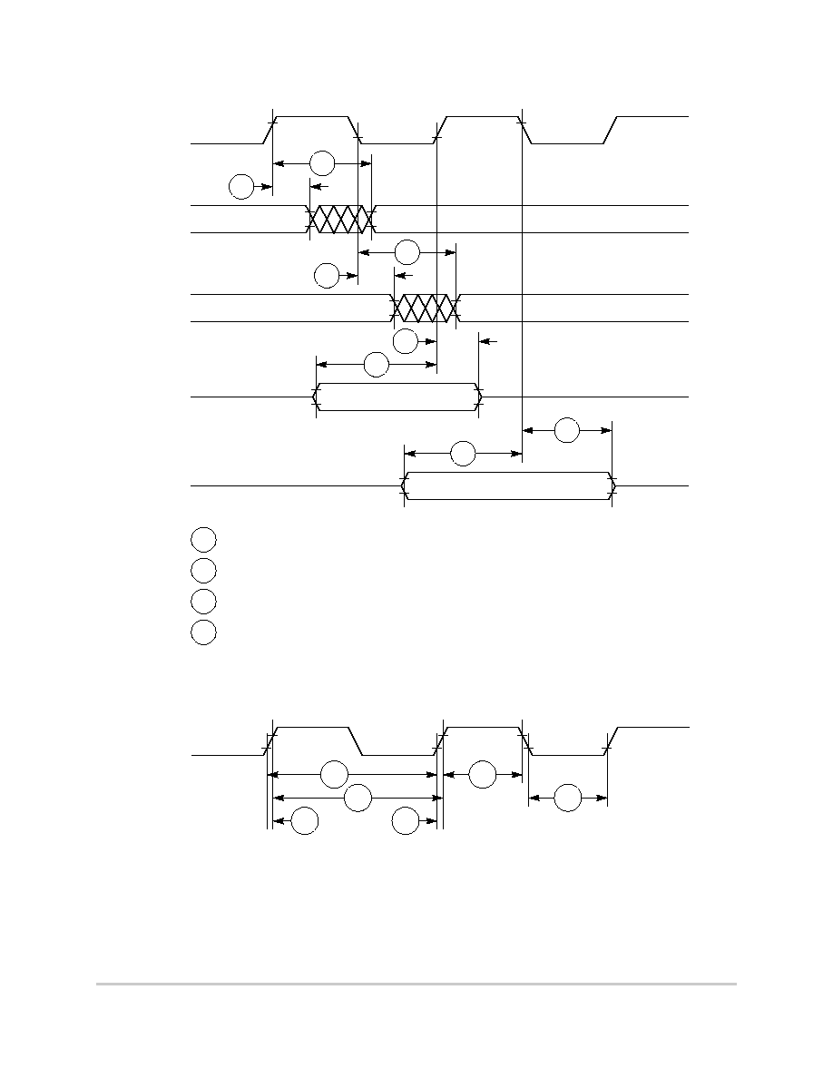
Figure 5 shows the control timing diagram.
Figure 5. Control Timing
Figure 6 shows the timing for the external clock.
Figure 6. External Clock Timing
CLKOUT
Outputs
A
B
2.0 V
0.8 V
0.8 V
2.0 V
2.0 V
0.8 V
2.0 V
0.8 V
Outputs
2.0 V
0.8 V
2.0 V
0.8 V
B
A
Inputs
2.0 V
0.8 V
2.0 V
0.8 V
D
C
Inputs
2.0 V
0.8 V
2.0 V
0.8 V
C
D
A
Maximum output delay specification
B
Minimum output hold time
C
Minimum input setup time specification
D
Minimum input hold time specification
CLKOUT
B1
B5
B3
B4
B1
B2
MOTOROLA
MPC866/859 Hardware Specifications
25
Bus Signal Timing
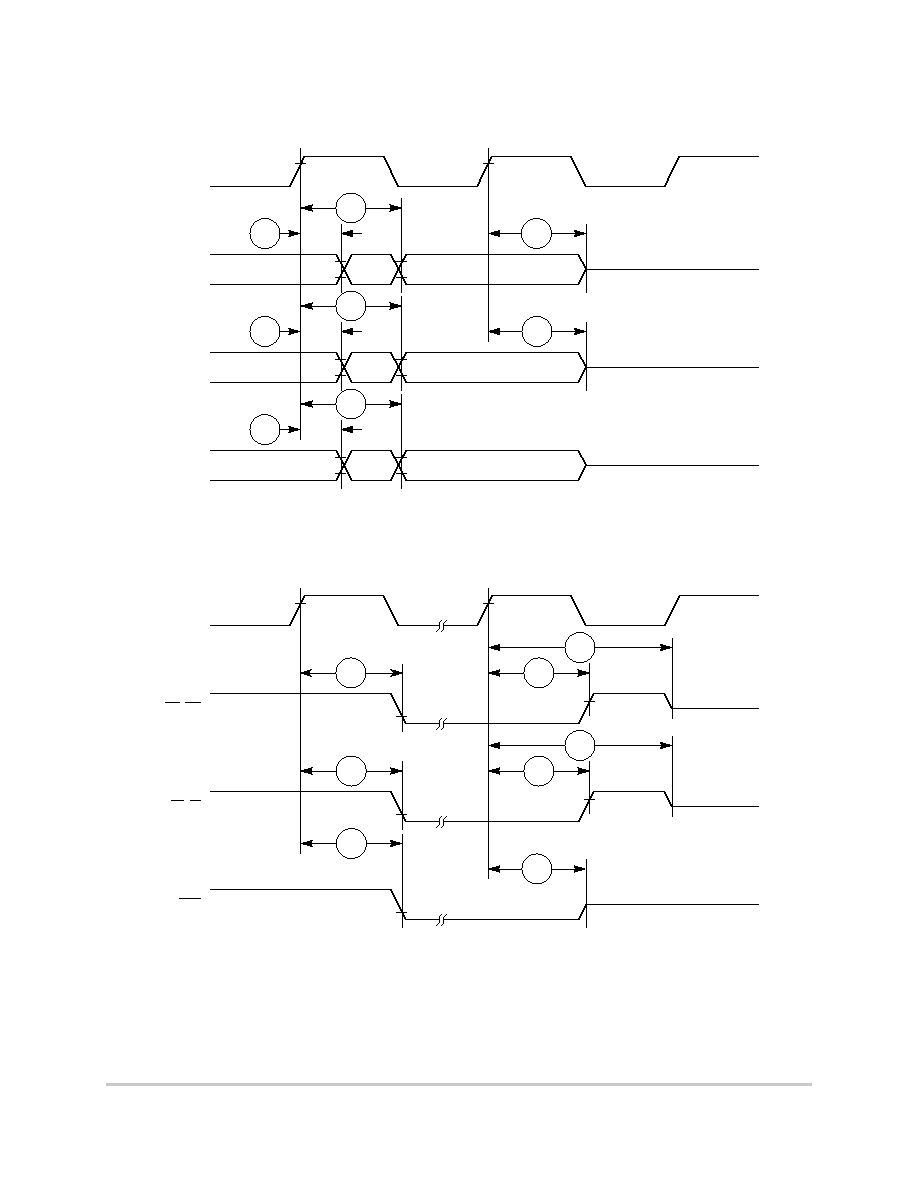
Figure 7 shows the timing for the synchronous output signals.
Figure 7. Synchronous Output Signals Timing
Figure 8 shows the timing for the synchronous active pull-up and open-drain output signals.
Figure 8. Synchronous Active Pull-Up Resistor and Open-Drain Output Signals Timing
CLKOUT
Output
Signals
Output
Signals
Output
Signals
B8
B7
B9
B8a
B9
B7a
B8b
B7b
CLKOUT
TS, BB
TA, BI
TEA
B13
B12
B11
B11a
B12a
B13a
B15
B14
26
MPC866/859 Hardware Specifications
MOTOROLA
Bus Signal Timing
Bus Signal Timing
Figure 9 shows the timing for the synchronous input signals.
Figure 9. Synchronous Input Signals Timing
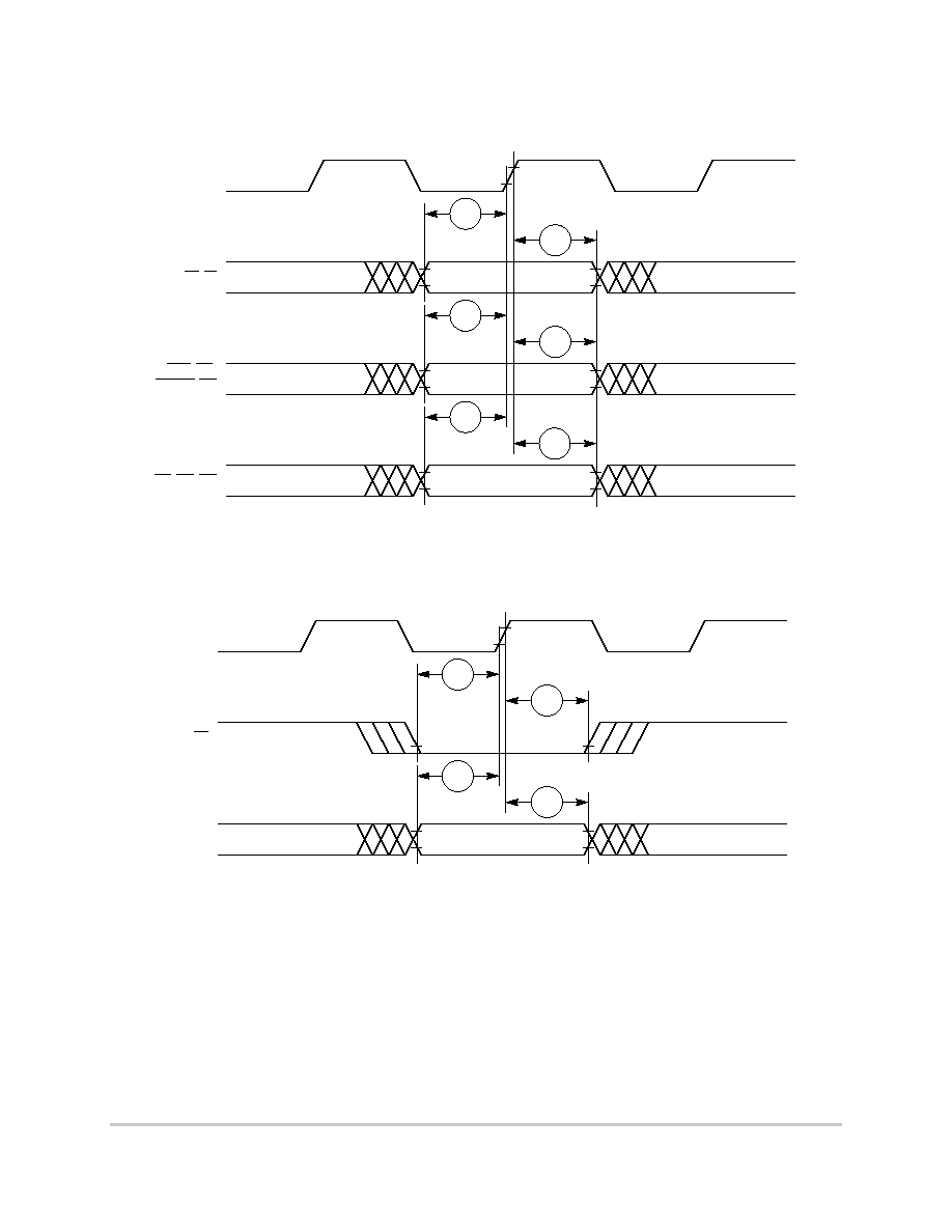
Figure 10 shows normal case timing for input data. It also applies to normal read accesses under the control
of the UPM in the memory controller.
Figure 10. Input Data Timing in Normal Case
CLKOUT
TA, BI
TEA, KR,
RETRY, CR
BB, BG, BR
B16
B17
B16a
B17a
B16b
B17
CLKOUT
TA
D[0:31],
DP[0:3]
B16
B17
B19
B18

MOTOROLA
MPC866/859 Hardware Specifications
27
Bus Signal Timing
Figure 11 shows the timing for the input data controlled by the UPM for data beats where DLT3 = 1 in the
UPM RAM words. (This is only the case where data is latched on the falling edge of CLKOUT.)
Figure 11. Input Data Timing when Controlled by UPM in the Memory Controller and DLT3 = 1
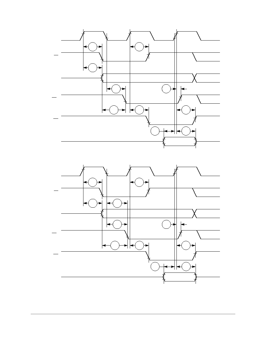
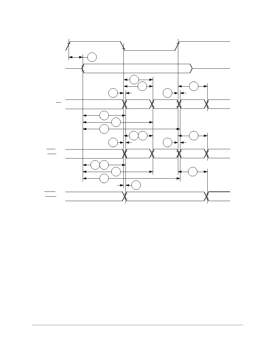
Figure 12 through Figure 15 show the timing for the external bus read controlled by various GPCM factors.
Figure 12. External Bus Read Timing (GPCM Controlled--ACS = 00)
CLKOUT
TA
D[0:31],
DP[0:3]
B20
B21
CLKOUT
A[0:31]
CSx
OE
WE[0:3]
TS
D[0:31],
DP[0:3]
B11
B12
B23
B8
B22
B26
B19
B18
B25
B28
28
MPC866/859 Hardware Specifications
MOTOROLA
Bus Signal Timing
Bus Signal Timing
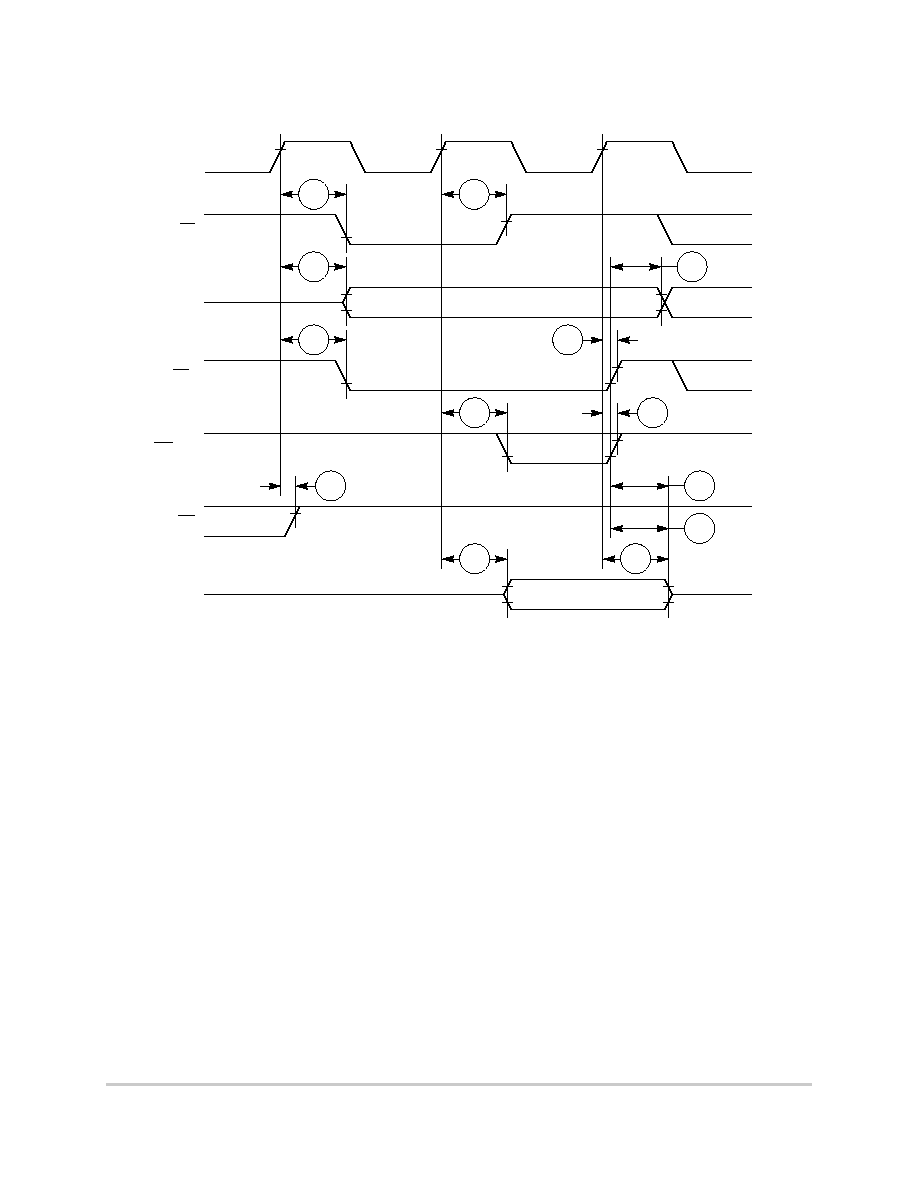
Figure 13. External Bus Read Timing (GPCM Controlled--TRLX = 0 or 1, ACS = 10)
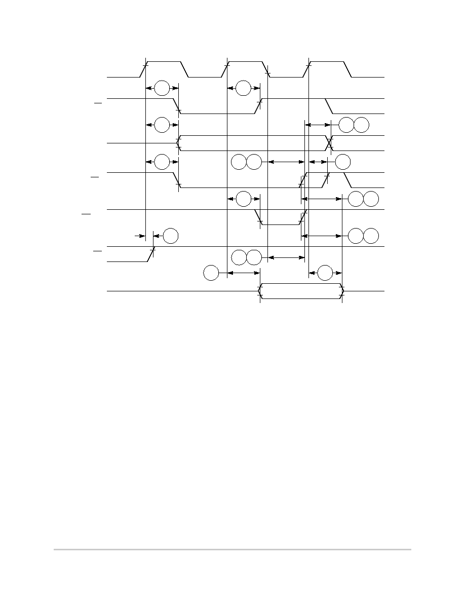
Figure 14. External Bus Read Timing (GPCM Controlled--TRLX = 0 or 1, ACS = 11)
CLKOUT
A[0:31]
CSx
OE
TS
D[0:31],
DP[0:3]
B11
B12
B8
B22a
B23
B26
B19
B18
B25
B24
CLKOUT
A[0:31]
CSx
OE
TS
D[0:31],
DP[0:3]
B11
B12
B22b
B8
B22c
B23
B24a
B25
B26
B19
B18

MOTOROLA
MPC866/859 Hardware Specifications
29
Bus Signal Timing
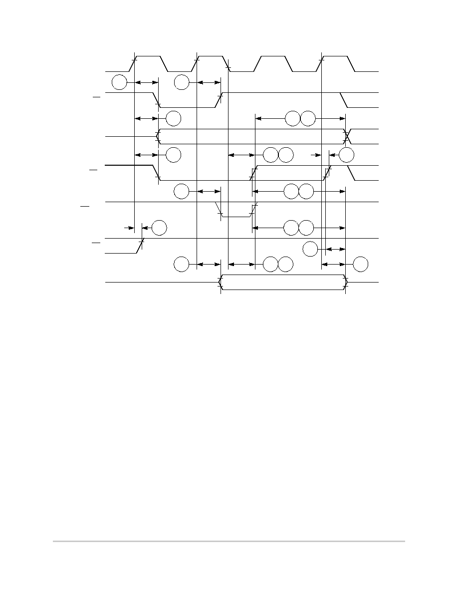
Figure 15. External Bus Read Timing (GPCM Controlled--TRLX = 0 or 1, ACS = 10, ACS = 11)
CLKOUT
A[0:31]
CSx
OE
TS
D[0:31],
DP[0:3]
B11
B12
B8
B22a
B27
B27a
B22b B22c
B19
B18
B26
B23
30
MPC866/859 Hardware Specifications
MOTOROLA
Bus Signal Timing
Bus Signal Timing
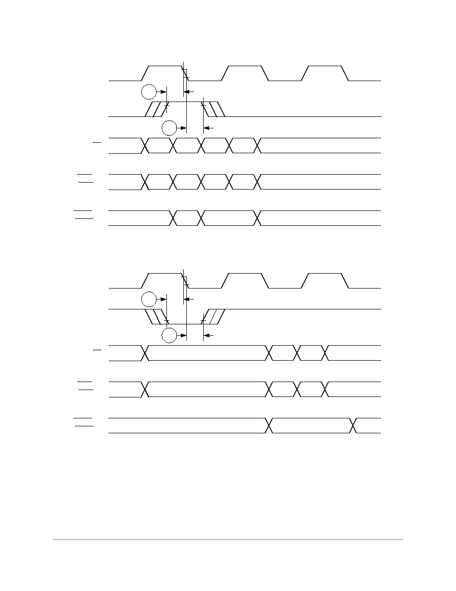
Figure 16 through Figure 18 show the timing for the external bus write controlled by various GPCM factors.
Figure 16. External Bus Write Timing (GPCM Controlled--TRLX = 0 or 1, CSNT = 0)
CLKOUT
A[0:31]
CSx
WE[0:3]
OE
TS
D[0:31],
DP[0:3]
B11
B8
B22
B23
B12
B30
B28
B25
B26
B8
B9
B29
B29b
MOTOROLA
MPC866/859 Hardware Specifications
31
Bus Signal Timing
Figure 17. External Bus Write Timing (GPCM Controlled--TRLX = 0, CSNT = 1)
B23
B30a B30c
CLKOUT
A[0:31]
CSx
OE
WE[0:3]
TS
D[0:31],
DP[0:3]
B11
B8
B22
B12
B28b B28d
B25
B26
B8
B28a
B9
B28c
B29c B29g
B29a B29f
32
MPC866/859 Hardware Specifications
MOTOROLA
Bus Signal Timing
Bus Signal Timing
Figure 18. External Bus Write Timing (GPCM Controlled--TRLX = 1, CSNT = 1)
B23
B22
B8
B12
B11
CLKOUT
A[0:31]
CSx
WE[0:3]
TS
OE
D[0:31],
DP[0:3]
B30d
B30b
B28b B28d
B25
B29e B29i
B26
B29d B29h
B28a B28c
B9
B8
B29b
MOTOROLA
MPC866/859 Hardware Specifications
33
Bus Signal Timing
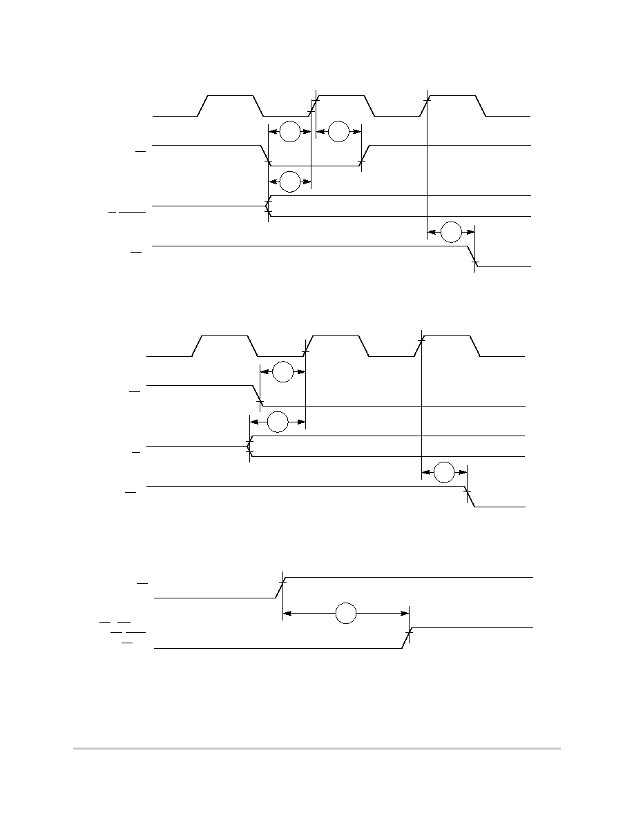
Figure 19 shows the timing for the external bus controlled by the UPM.
Figure 19. External Bus Timing (UPM Controlled Signals)
CLKOUT
CSx
B31d
B8
B31
B34
B32b
GPL_A[0:5],
GPL_B[0:5]
BS_A[0:3],
BS_B[0:3]
A[0:31]
B31c
B31b
B34a
B32
B32a B32d
B34b
B36
B35b
B35a
B35
B33
B32c
B33a
B31a
34
MPC866/859 Hardware Specifications
MOTOROLA
Bus Signal Timing
Bus Signal Timing
Figure 20 shows the timing for the asynchronous asserted UPWAIT signal controlled by the UPM.
Figure 20. Asynchronous UPWAIT Asserted Detection in UPM Handled Cycles Timing
Figure 21 shows the timing for the asynchronous negated UPWAIT signal controlled by the UPM.
Figure 21. Asynchronous UPWAIT Negated Detection in UPM Handled Cycles Timing
CLKOUT
CSx
UPWAIT
GPL_A[0:5],
GPL_B[0:5]
BS_A[0:3],
BS_B[0:3]
B37
B38
CLKOUT
CSx
UPWAIT
GPL_A[0:5],
GPL_B[0:5]
BS_A[0:3],
BS_B[0:3]
B37
B38
MOTOROLA
MPC866/859 Hardware Specifications
35
Bus Signal Timing
Figure 22 shows the timing for the synchronous external master access controlled by the GPCM.
Figure 22. Synchronous External Master Access Timing (GPCM Handled ACS = 00)
Figure 23 shows the timing for the asynchronous external master memory access controlled by the GPCM.
Figure 23. Asynchronous External Master Memory Access Timing (GPCM Controlled--ACS = 00)
Figure 24 shows the timing for the asynchronous external master control signals negation.
Figure 24. Asynchronous External Master--Control Signals Negation Timing
CLKOUT
TS
A[0:31],
TSIZ[0:1],
R/W, BURST
CSx
B41
B42
B40
B22
CLKOUT
AS
A[0:31],
TSIZ[0:1],
R/W
CSx
B39
B40
B22
AS
CSx, WE[0:3],
OE, GPLx,
BS[0:3]
B43

36
MPC866/859 Hardware Specifications
MOTOROLA
Bus Signal Timing
Bus Signal Timing
Table 10 shows the interrupt timing for the MPC866/859.
Figure 25 shows the interrupt detection timing for the external level-sensitive lines.
Figure 25. Interrupt Detection Timing for External Level Sensitive Lines
Figure 26 shows the interrupt detection timing for the external edge-sensitive lines.
Figure 26. Interrupt Detection Timing for External Edge Sensitive Lines
Table 10. Interrupt Timing
Num
Characteristic
1
1
The timings I39 and I40 describe the testing conditions under which the IRQ lines are tested when being defined as
level sensitive. The IRQ lines are synchronized internally and do not have to be asserted or negated with reference
to the CLKOUT.
The timings I41, I42, and I43 are specified to allow the correct function of the IRQ lines detection circuitry, and has
no direct relation with the total system interrupt latency that the MPC866/859 is able to support.
All Frequencies
Unit
Min
Max
I39
IRQx valid to CLKOUT rising edge (setup time)
6.00
--
ns
I40
IRQx hold time after CLKOUT
2.00
--
ns
I41
IRQx pulse width low
3.00
--
ns
I42
IRQx pulse width high
3.00
--
ns
I43
IRQx edge-to-edge time
4xT
CLOCKOUT
--
--
CLKOUT
IRQx
I39
I40
CLKOUT
IRQx
I41
I42
I43
I43
MOTOROLA
MPC866/859 Hardware Specifications
37
Bus Signal Timing
Table 11 shows the PCMCIA timing for the MPC866/859.
Table 11. PCMCIA Timing
Num
Characteristic
33 MHz
40 MHz
50 MHz
66 MHz
Unit
Min
Max
Min
Max
Min
Max
Min
Max
P44
A(0:31), REG valid to PCMCIA
Strobe asserted
1
(MIN = 0.75 x B1
≠ 2.00)
1
PSST = 1. Otherwise, add PSST times cycle time.
PSHT = 0. Otherwise, add PSHT times cycle time.
These synchronous timings define when the WAITx signals are detected in order to freeze (or relieve) the PCMCIA
current cycle. The WAITx assertion will be effective only if it is detected 2 cycles before the PSL timer expiration. See
PCMCIA Interface in the MPC866 PowerQUICC User's Manual.
20.70
--
16.70
--
13.00
--
9.40
--
ns
P45
A(0:31), REG valid to ALE
negation
1
(MIN = 1.00 x B1 ≠ 2.00)
28.30
--
23.00
--
18.00
--
13.20
--
ns
P46
CLKOUT to REG valid (MAX = 0.25
x B1 + 8.00)
7.60
15.60
6.30
14.30
5.00
13.00
3.80
11.80
ns
P47
CLKOUT to REG invalid (MIN =
0.25 x B1 + 1.00)
8.60
--
7.30
--
6.00
--
4.80
--
ns
P48
CLKOUT to CE1, CE2 asserted
(MAX = 0.25 x B1 + 8.00)
7.60
15.60
6.30
14.30
5.00
13.00
3.80
11.80
ns
P49
CLKOUT to CE1, CE2 negated
(MAX = 0.25 x B1 + 8.00)
7.60
15.60
6.30
14.30
5.00
13.00
3.80
11.80
ns
P50
CLKOUT to PCOE, IORD, PCWE,
IOWR assert time (MAX = 0.00 x
B1 + 11.00)
--
11.00
--
11.00
--
11.00
--
11.00
ns
P51
CLKOUT to PCOE, IORD, PCWE,
IOWR negate time (MAX = 0.00 x
B1 + 11.00)
2.00
11.00
2.00
11.00
2.00
11.00
2.00
11.00
ns
P52
CLKOUT to ALE assert time (MAX
= 0.25 x B1 + 6.30)
7.60
13.80
6.30
12.50
5.00
11.30
3.80
10.00
ns
P53
CLKOUT to ALE negate time (MAX
= 0.25 x B1 + 8.00)
--
15.60
--
14.30
--
13.00
--
11.80
ns
P54
PCWE, IOWR negated to D(0:31)
invalid
1
(MIN = 0.25 x B1 ≠ 2.00)
5.60
--
4.30
--
3.00
--
1.80
--
ns
P55
WAITA and WAITB valid to
CLKOUT rising edge
1
(MIN = 0.00
x B1 + 8.00)
8.00
--
8.00
--
8.00
--
8.00
--
ns
P56
CLKOUT rising edge to WAITA and
WAITB invalid
1
(MIN = 0.00 x B1 +
2.00)
2.00
--
2.00
--
2.00
--
2.00
--
ns
38
MPC866/859 Hardware Specifications
MOTOROLA
Bus Signal Timing
Bus Signal Timing
Figure 27 shows the PCMCIA access cycle timing for the external bus read.
Figure 27. PCMCIA Access Cycles Timing External Bus Read
CLKOUT
A[0:31]
REG
CE1/CE2
PCOE, IORD
TS
D[0:31]
ALE
B19
B18
P53
P52
P52
P51
P50
P48
P49
P46
P45
P44
P47
MOTOROLA
MPC866/859 Hardware Specifications
39
Bus Signal Timing
Figure 28 shows the PCMCIA access cycle timing for the external bus write.
Figure 28. PCMCIA Access Cycles Timing External Bus Write
Figure 29 shows the PCMCIA WAIT signals detection timing.
Figure 29. PCMCIA WAIT Signals Detection Timing
CLKOUT
A[0:31]
REG
CE1/CE2
PCWE, IOWR
TS
D[0:31]
ALE
B9
B8
P53
P52
P52
P51
P50
P48
P49
P46
P45
P44
P47
P54
CLKOUT
WAITx
P55
P56
40
MPC866/859 Hardware Specifications
MOTOROLA
Bus Signal Timing
Bus Signal Timing
Table 12 shows the PCMCIA port timing for the MPC866/859.
Figure 30 shows the PCMCIA output port timing for the MPC866/859.
Figure 30. PCMCIA Output Port Timing
Figure 31 shows the PCMCIA output port timing for the MPC866/859.
Figure 31. PCMCIA Input Port Timing
Table 12. PCMCIA Port Timing
Num
Characteristic
33 MHz
40 MHz
50 MHz
66 MHz
Unit
Min
Max
Min
Max
Min
Max
Min
Max
P57
CLKOUT to OPx, valid (MAX = 0.00 x B1
+ 19.00)
--
19.00
--
19.00
--
19.00
--
19.00
ns
P58
HRESET negated to OPx drive
1
(MIN =
0.75 x B1 + 3.00)
1
OP2 and OP3 only.
25.70
--
21.70
--
18.00
--
14.40
--
ns
P59
IP_Xx valid to CLKOUT rising edge (MIN
= 0.00 x B1 + 5.00)
5.00
--
5.00
--
5.00
--
5.00
--
ns
P60
CLKOUT rising edge to IP_Xx invalid
(MIN = 0.00 x B1 + 1.00)
1.00
--
1.00
--
1.00
--
1.00
--
ns
CLKOUT
HRESET
Output
Signals
OP2, OP3
P57
P58
CLKOUT
Input
Signals
P59
P60
MOTOROLA
MPC866/859 Hardware Specifications
41
Bus Signal Timing
Table 13 shows the debug port timing for the MPC866/859.
Figure 32 shows the input timing for the debug port clock.
Figure 32. Debug Port Clock Input Timing
Figure 33 shows the timing for the debug port.
Figure 33. Debug Port Timings
Table 13. Debug Port Timing
Num
Characteristic
All Frequencies
Unit
Min
Max
D61
DSCK cycle time
3xT
CLOCKOUT
--
D62
DSCK clock pulse width
1.25xT
CLOCKOUT
--
D63
DSCK rise and fall times
0.00
3.00
ns
D64
DSDI input data setup time
8.00
--
ns
D65
DSDI data hold time
5.00
--
ns
D66
DSCK low to DSDO data valid
0.00
15.00
ns
D67
DSCK low to DSDO invalid
0.00
2.00
ns
DSCK
D61
D61
D63
D62
D62
D63
DSCK
DSDI
DSDO
D64
D65
D66
D67
42
MPC866/859 Hardware Specifications
MOTOROLA
Bus Signal Timing
Bus Signal Timing
Table 14 shows the reset timing for the MPC866/859.
Table 14. Reset Timing
Num
Characteristic
33 MHz
40 MHz
50 MHz
66 MHz
Unit
Min
Max
Min
Max
Min
Max
Min
Max
R69
CLKOUT to HRESET high impedance
(MAX = 0.00 x B1 + 20.00)
--
20.00
--
20.00
--
20.00
--
20.00
ns
R70
CLKOUT to SRESET high impedance
(MAX = 0.00 x B1 + 20.00)
--
20.00
--
20.00
--
20.00
--
20.00
ns
R71
RSTCONF pulse width (MIN = 17.00 x
B1)
515.20
--
425.00
--
340.00
--
257.60
--
ns
R72
--
--
--
--
--
--
--
--
--
--
R73
Configuration data to HRESET rising
edge setup time (MIN = 15.00 x B1 +
50.00)
504.50
--
425.00
--
350.00
--
277.30
--
ns
R74
Configuration data to RSTCONF rising
edge setup time (MIN = 0.00 x B1 +
350.00)
350.00
--
350.00
--
350.00
--
350.00
--
ns
R75
Configuration data hold time after
RSTCONF negation (MIN = 0.00 x B1 +
0.00)
0.00
--
0.00
--
0.00
--
0.00
--
ns
R76
Configuration data hold time after
HRESET negation (MIN = 0.00 x B1 +
0.00)
0.00
--
0.00
--
0.00
--
0.00
--
ns
R77
HRESET and RSTCONF asserted to
data out drive (MAX = 0.00 x B1 +
25.00)
--
25.00
--
25.00
--
25.00
--
25.00
ns
R78
RSTCONF negated to data out high
impedance (MAX = 0.00 x B1 + 25.00)
--
25.00
--
25.00
--
25.00
--
25.00
ns
R79
CLKOUT of last rising edge before chip
three-states HRESET to data out high
impedance (MAX = 0.00 x B1 + 25.00)
--
25.00
--
25.00
--
25.00
--
25.00
ns
R80
DSDI, DSCK setup (MIN = 3.00 x B1)
90.90
--
75.00
--
60.00
--
45.50
--
ns
R81
DSDI, DSCK hold time (MIN = 0.00 x B1
+ 0.00)
0.00
--
0.00
--
0.00
--
0.00
--
ns
R82
SRESET negated to CLKOUT rising
edge for DSDI and DSCK sample (MIN
= 8.00 x B1)
242.40
--
200.00
--
160.00
--
121.20
--
ns
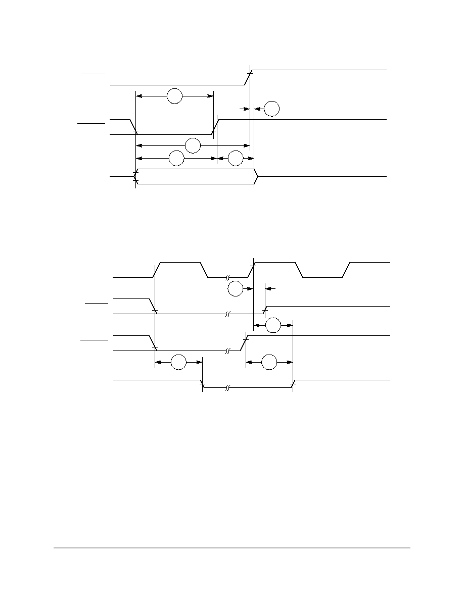
MOTOROLA
MPC866/859 Hardware Specifications
43
Bus Signal Timing
Figure 34 shows the reset timing for the data bus configuration.
Figure 34. Reset Timing--Configuration from Data Bus
Figure 35 shows the reset timing for the data bus weak drive during configuration.
Figure 35. Reset Timing--Data Bus Weak Drive During Configuration
HRESET
RSTCONF
D[0:31] (IN)
R71
R74
R73
R75
R76
CLKOUT
HRESET
D[0:31] (OUT)
(Weak)
RSTCONF
R69
R79
R77
R78
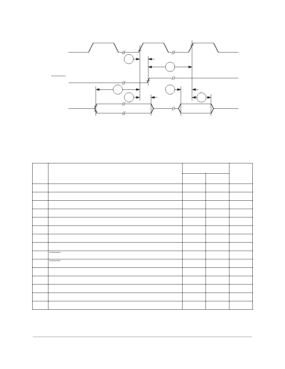
44
MPC866/859 Hardware Specifications
MOTOROLA
IEEE 1149.1 Electrical Specifications
IEEE 1149.1 Electrical Specifications
Figure 36 shows the reset timing for the debug port configuration.
Figure 36. Reset Timing--Debug Port Configuration
11
IEEE 1149.1 Electrical Specifications
Table 15 shows the JTAG timings for the MPC866/859 shown in Figure 37 through Figure 40.
Table 15. JTAG Timing
Num
Characteristic
All Frequencies
Unit
Min
Max
J82
TCK cycle time
100.00
--
ns
J83
TCK clock pulse width measured at 1.5 V
40.00
--
ns
J84
TCK rise and fall times
0.00
10.00
ns
J85
TMS, TDI data setup time
5.00
--
ns
J86
TMS, TDI data hold time
25.00
--
ns
J87
TCK low to TDO data valid
--
27.00
ns
J88
TCK low to TDO data invalid
0.00
--
ns
J89
TCK low to TDO high impedance
--
20.00
ns
J90
TRST assert time
100.00
--
ns
J91
TRST setup time to TCK low
40.00
--
ns
J92
TCK falling edge to output valid
--
50.00
ns
J93
TCK falling edge to output valid out of high impedance
--
50.00
ns
J94
TCK falling edge to output high impedance
--
50.00
ns
J95
Boundary scan input valid to TCK rising edge
50.00
--
ns
J96
TCK rising edge to boundary scan input invalid
50.00
--
ns
CLKOUT
SRESET
DSCK, DSDI
R70
R82
R80
R80
R81
R81
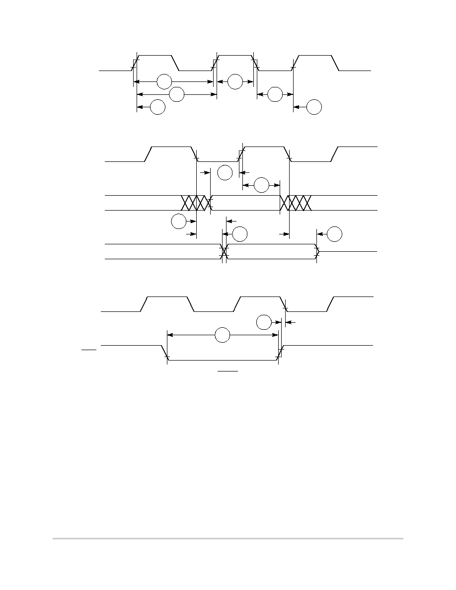
MOTOROLA
MPC866/859 Hardware Specifications
45
IEEE 1149.1 Electrical Specifications
Figure 37. JTAG Test Clock Input Timing
Figure 38. JTAG Test Access Port Timing Diagram
Figure 39. JTAG TRST Timing Diagram
TCK
J82
J83
J82
J83
J84
J84
TCK
TMS, TDI
TDO
J85
J86
J87
J88
J89
TCK
TRST
J91
J90
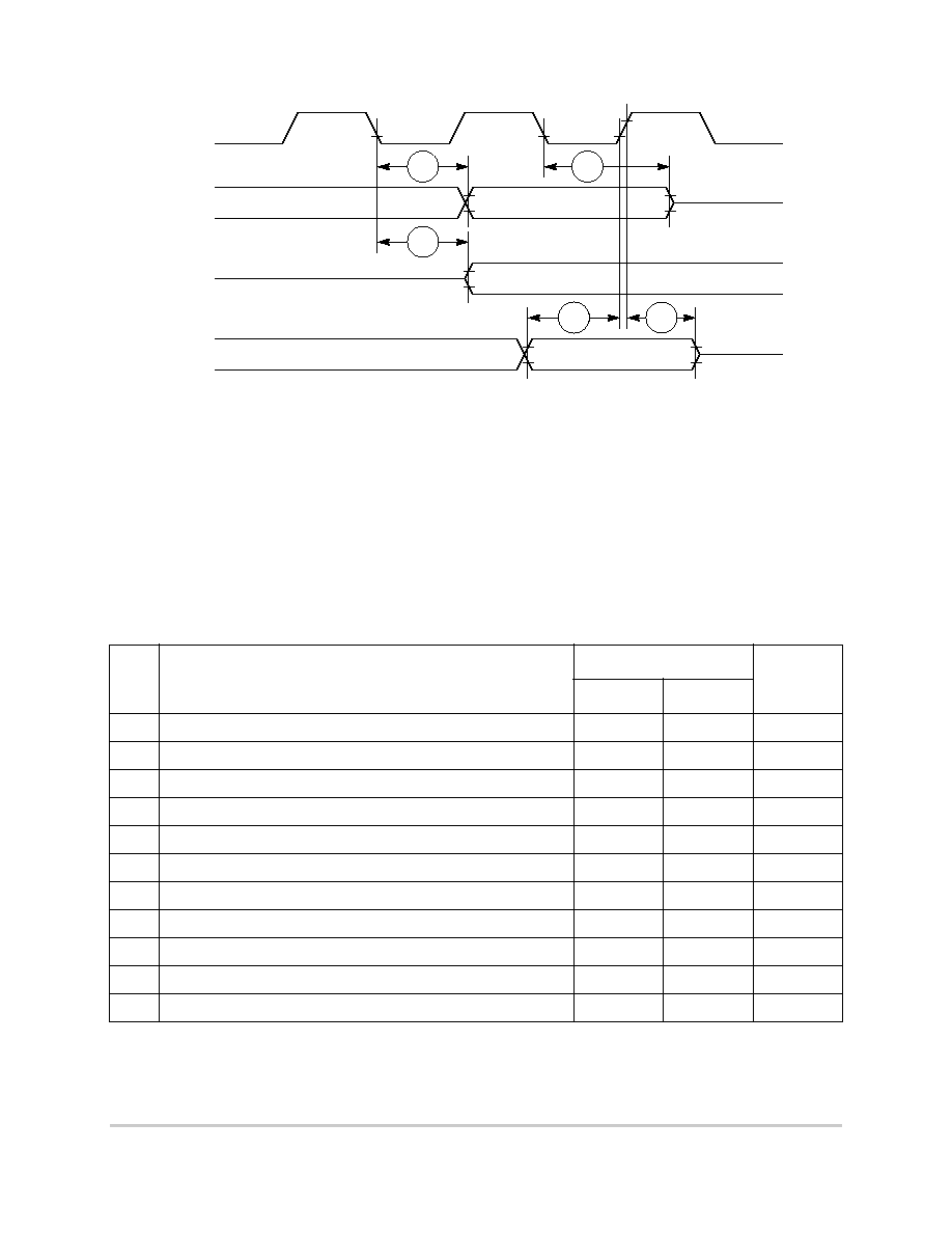
46
MPC866/859 Hardware Specifications
MOTOROLA
CPM Electrical Characteristics
CPM Electrical Characteristics
Figure 40. Boundary Scan (JTAG) Timing Diagram
12
CPM Electrical Characteristics
This section provides the AC and DC electrical specifications for the communications processor module
(CPM) of the MPC866/859.
12.1
PIP/PIO AC Electrical Specifications
Table 16 shows the PIP/PIO AC timings as shown in Figure 41 through Figure 45.
Table 16. PIP/PIO Timing
Num
Characteristic
All Frequencies
Unit
Min
Max
21
Data-in setup time to STBI low
0
--
ns
22
Data-In hold time to STBI high
2.5 ≠ t3
1
1
t3 = Specification 23
--
clk
23
STBI pulse width
1.5
--
clk
24
STBO pulse width
1 clk ≠ 5ns
--
ns
25
Data-out setup time to STBO low
2
--
clk
26
Data-out hold time from STBO high
5
--
clk
27
STBI low to STBO low (Rx interlock)
--
2
clk
28
STBI low to STBO high (Tx interlock)
2
--
clk
29
Data-in setup time to clock high
15
--
ns
30
Data-in hold time from clock high
7.5
--
ns
31
Clock low to data-out valid (CPU writes data, control, or direction)
--
25
ns
TCK
Output
Signals
Output
Signals
Output
Signals
J92
J94
J93
J95
J96
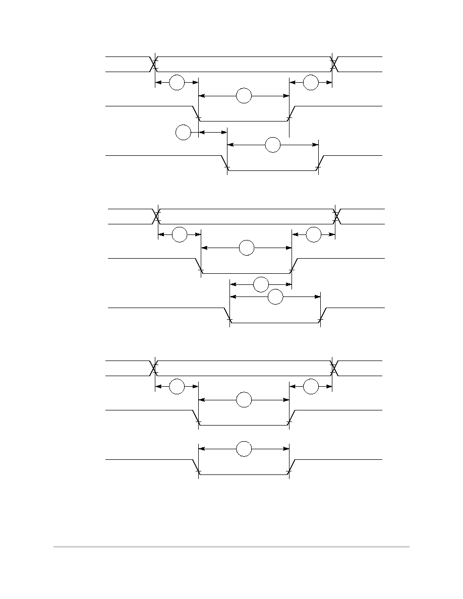
MOTOROLA
MPC866/859 Hardware Specifications
47
CPM Electrical Characteristics
Figure 41. PIP Rx (Interlock Mode) Timing Diagram
Figure 42. PIP Tx (Interlock Mode) Timing Diagram
Figure 43. PIP Rx (Pulse Mode) Timing Diagram
DATA-IN
STBI
23
24
22
STBO
27
21
DATA-OUT
24
23
26
28
25
STBO
(Output)
STBI
(Input)
DATA-IN
23
22
21
STBI
(Input)
STBO
(Output)
24
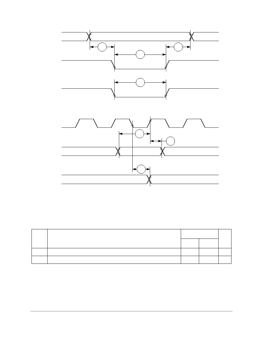
48
MPC866/859 Hardware Specifications
MOTOROLA
CPM Electrical Characteristics
CPM Electrical Characteristics
Figure 44. PIP TX (Pulse Mode) Timing Diagram
Figure 45. Parallel I/O Data-In/Data-Out Timing Diagram
12.2
Port C Interrupt AC Electrical Specifications
Table 17 shows timings for port C interrupts.
Table 17. Port C Interrupt Timing
Num
Characteristic
33.34 MHz
Unit
Min
Max
35
Port C interrupt pulse width low (edge-triggered mode)
55
--
ns
36
Port C interrupt minimum time between active edges
55
--
ns
DATA-OUT
24
26
25
STBO
(Output)
STBI
(Input)
23
CLKO
DATA-IN
29
31
30
DATA-OUT
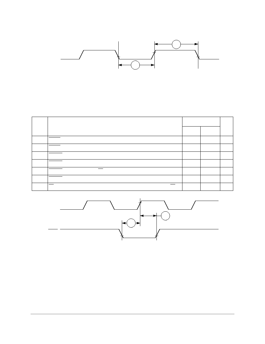
MOTOROLA
MPC866/859 Hardware Specifications
49
CPM Electrical Characteristics
Figure 46 shows the port C interrupt detection timing.
Figure 46. Port C Interrupt Detection Timing
12.3
IDMA Controller AC Electrical Specifications
Table 18 shows the IDMA controller timings as shown in Figure 47 through Figure 50.
Figure 47. IDMA External Requests Timing Diagram
Table 18. IDMA Controller Timing
Num
Characteristic
All Frequencies
Unit
Min
Max
40
DREQ setup time to clock high
7
--
ns
41
DREQ hold time from clock high
3
--
ns
42
SDACK assertion delay from clock high
--
12
ns
43
SDACK negation delay from clock low
--
12
ns
44
SDACK negation delay from TA low
--
20
ns
45
SDACK negation delay from clock high
--
15
ns
46
TA assertion to falling edge of the clock setup time (applies to external TA)
7
--
ns
Port C
35
36
(Input)
41
40
DREQ
(Input)
CLKO
(Output)
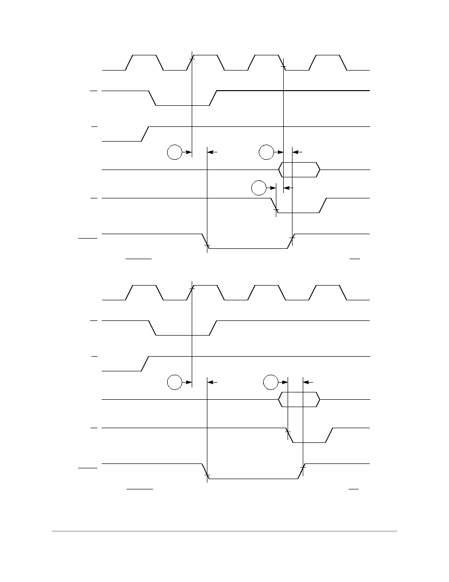
50
MPC866/859 Hardware Specifications
MOTOROLA
CPM Electrical Characteristics
CPM Electrical Characteristics
Figure 48. SDACK Timing Diagram--Peripheral Write, Externally-Generated TA
Figure 49. SDACK Timing Diagram--Peripheral Write, Internally-Generated TA
DATA
42
46
43
CLKO
(Output)
TS
(Output)
R/W
(Output)
TA
(Input)
SDACK
DATA
42
44
CLKO
(Output)
TS
(Output)
R/W
(Output)
TA
(Output)
SDACK
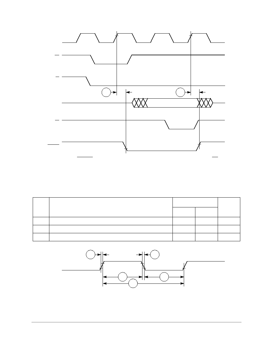
MOTOROLA
MPC866/859 Hardware Specifications
51
CPM Electrical Characteristics
Figure 50. SDACK Timing Diagram--Peripheral Read, Internally-Generated TA
12.4
Baud Rate Generator AC Electrical Specifications
Table 19 shows the baud rate generator timings as shown in Figure 51.
Figure 51. Baud Rate Generator Timing Diagram
Table 19. Baud Rate Generator Timing
Num
Characteristic
All Frequencies
Unit
Min
Max
50
BRGO rise and fall time
--
10
ns
51
BRGO duty cycle
40
60
%
52
BRGO cycle
40
--
ns
DATA
42
45
CLKO
(Output)
TS
(Output)
R/W
(Output)
TA
(Output)
SDACK
52
50
51
BRGOX
50
51

52
MPC866/859 Hardware Specifications
MOTOROLA
CPM Electrical Characteristics
CPM Electrical Characteristics
12.5
Timer AC Electrical Specifications
Table 20 shows the general-purpose timer timings as shown in Figure 52.
Figure 52. CPM General-Purpose Timers Timing Diagram
12.6
Serial Interface AC Electrical Specifications
Table 21 shows the serial interface timings as shown in Figure 53 through Figure 57.
Table 20. Timer Timing
Num
Characteristic
All Frequencies
Unit
Min
Max
61
TIN/TGATE rise and fall time
10
--
ns
62
TIN/TGATE low time
1
--
clk
63
TIN/TGATE high time
2
--
clk
64
TIN/TGATE cycle time
3
--
clk
65
CLKO low to TOUT valid
3
25
ns
Table 21. SI Timing
Num
Characteristic
All Frequencies
Unit
Min
Max
70
L1RCLK, L1TCLK frequency (DSC = 0)
1,
2
--
SYNCCLK/2.5
MHz
71
L1RCLK, L1TCLK width low (DSC = 0)
2
P + 10
--
ns
71a
L1RCLK, L1TCLK width high (DSC = 0)
3
P + 10
--
ns
72
L1TXD, L1ST(1≠4), L1RQ, L1CLKO rise/fall time
--
15.00
ns
73
L1RSYNC, L1TSYNC valid to L1CLK edge (SYNC
setup time)
20.00
--
ns
74
L1CLK edge to L1RSYNC, L1TSYNC, invalid
(SYNC hold time)
35.00
--
ns
CLKO
TIN/TGATE
(Input)
TOUT
(Output)
64
65
61
62
63
61
60
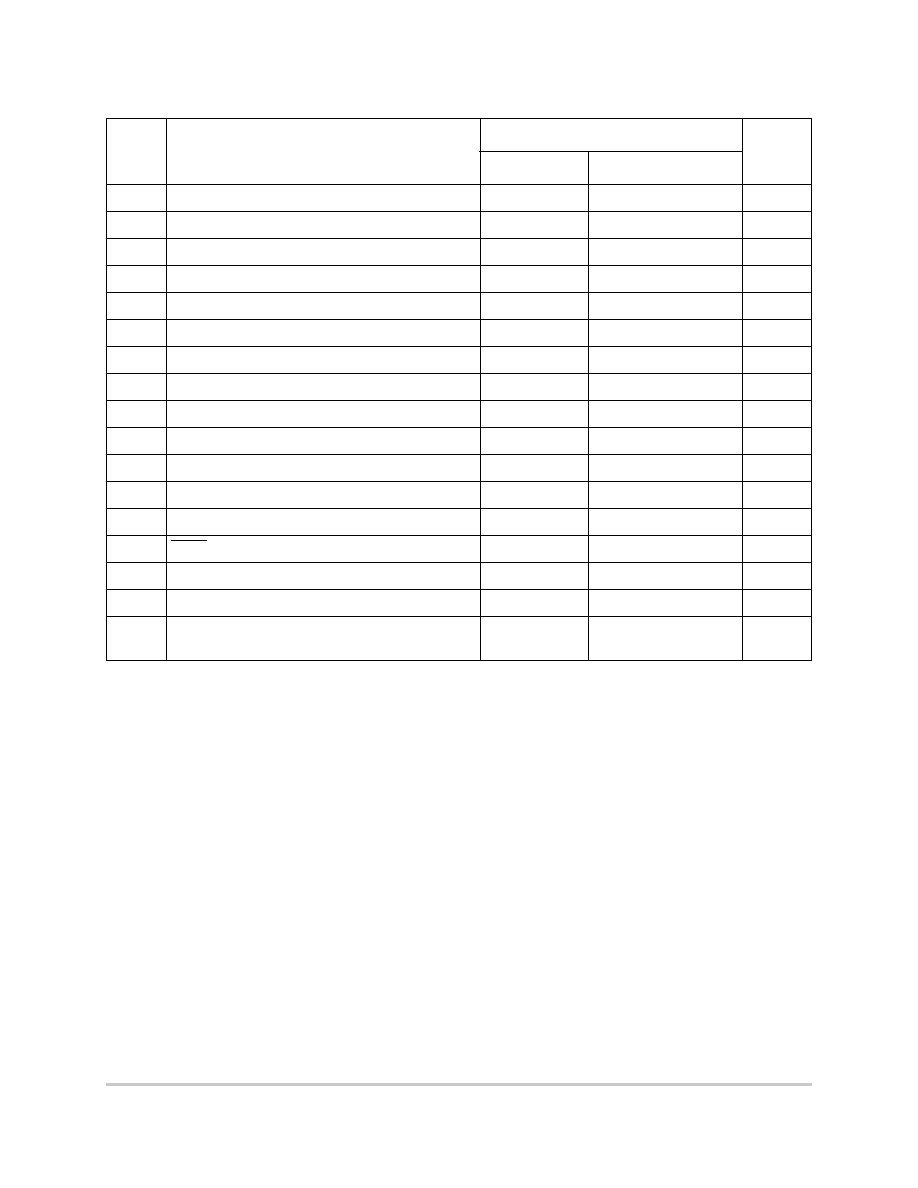
MOTOROLA
MPC866/859 Hardware Specifications
53
CPM Electrical Characteristics
75
L1RSYNC, L1TSYNC rise/fall time
--
15.00
ns
76
L1RXD valid to L1CLK edge (L1RXD setup time)
17.00
--
ns
77
L1CLK edge to L1RXD invalid (L1RXD hold time)
13.00
--
ns
78
L1CLK edge to L1ST(1≠4) valid
4
10.00
45.00
ns
78A
L1SYNC valid to L1ST(1≠4) valid
10.00
45.00
ns
79
L1CLK edge to L1ST(1≠4) invalid
10.00
45.00
ns
80
L1CLK edge to L1TXD valid
10.00
55.00
ns
80A
L1TSYNC valid to L1TXD valid
4
10.00
55.00
ns
81
L1CLK edge to L1TXD high impedance
0.00
42.00
ns
82
L1RCLK, L1TCLK frequency (DSC =1)
--
16.00 or SYNCCLK/2
MHz
83
L1RCLK, L1TCLK width low (DSC =1)
P + 10
--
ns
83a
L1RCLK, L1TCLK width high (DSC = 1)
3
P + 10
--
ns
84
L1CLK edge to L1CLKO valid (DSC = 1)
--
30.00
ns
85
L1RQ valid before falling edge of L1TSYNC
4
1.00
--
L1TCLK
86
L1GR setup time
2
42.00
--
ns
87
L1GR hold time
42.00
--
ns
88
L1CLK edge to L1SYNC valid (FSD = 00) CNT =
0000, BYT = 0, DSC = 0)
--
0.00
ns
1
The ratio SyncCLK/L1RCLK must be greater than 2.5/1.
2
These specs are valid for IDL mode only.
3
Where P = 1/CLKOUT. Thus, for a 25-MHz CLKO1 rate, P = 40 ns.
4
These strobes and TxD on the first bit of the frame become valid after L1CLK edge or L1SYNC, whichever is later.
Table 21. SI Timing (continued)
Num
Characteristic
All Frequencies
Unit
Min
Max

54
MPC866/859 Hardware Specifications
MOTOROLA
CPM Electrical Characteristics
CPM Electrical Characteristics
Figure 53. SI Receive Timing Diagram with Normal Clocking (DSC = 0)
L1RXD
(Input)
L1RCLK
(FE=0, CE=0)
(Input)
L1RCLK
(FE=1, CE=1)
(Input)
L1RSYNC
(Input)
L1ST(4-1)
(Output)
71
72
70
71a
RFSD=1
75
73
74
77
78
76
79
BIT0
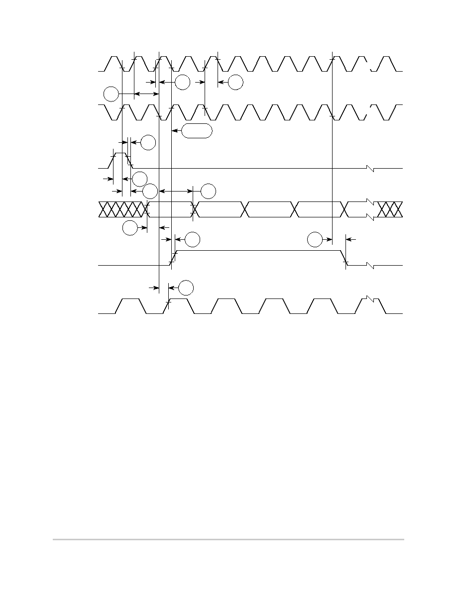
MOTOROLA
MPC866/859 Hardware Specifications
55
CPM Electrical Characteristics
Figure 54. SI Receive Timing with Double-Speed Clocking (DSC = 1)
L1RXD
(Input)
L1RCLK
(FE=1, CE=1)
(Input)
L1RCLK
(FE=0, CE=0)
(Input)
L1RSYNC
(Input)
L1ST(4-1)
(Output)
72
RFSD=1
75
73
74
77
78
76
79
83a
82
L1CLKO
(Output)
84
BIT0
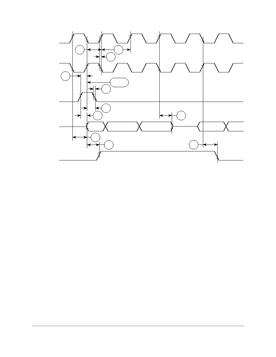
56
MPC866/859 Hardware Specifications
MOTOROLA
CPM Electrical Characteristics
CPM Electrical Characteristics
Figure 55. SI Transmit Timing Diagram (DSC = 0)
L1TXD
(Output)
L1TCLK
(FE=0, CE=0)
(Input)
L1TCLK
(FE=1, CE=1)
(Input)
L1TSYNC
(Input)
L1ST(4-1)
(Output)
71
70
72
73
75
74
80a
80
78
TFSD=0
81
79
BIT0
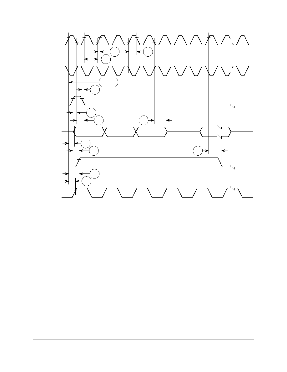
MOTOROLA
MPC866/859 Hardware Specifications
57
CPM Electrical Characteristics
Figure 56. SI Transmit Timing with Double Speed Clocking (DSC = 1)
L1TXD
(Output)
L1RCLK
(FE=0, CE=0)
(Input)
L1RCLK
(FE=1, CE=1)
(Input)
L1RSYNC
(Input)
L1ST(4-1)
(Output)
72
TFSD=0
75
73
74
78a
80
79
83a
82
L1CLKO
(Output)
84
BIT0
78
81
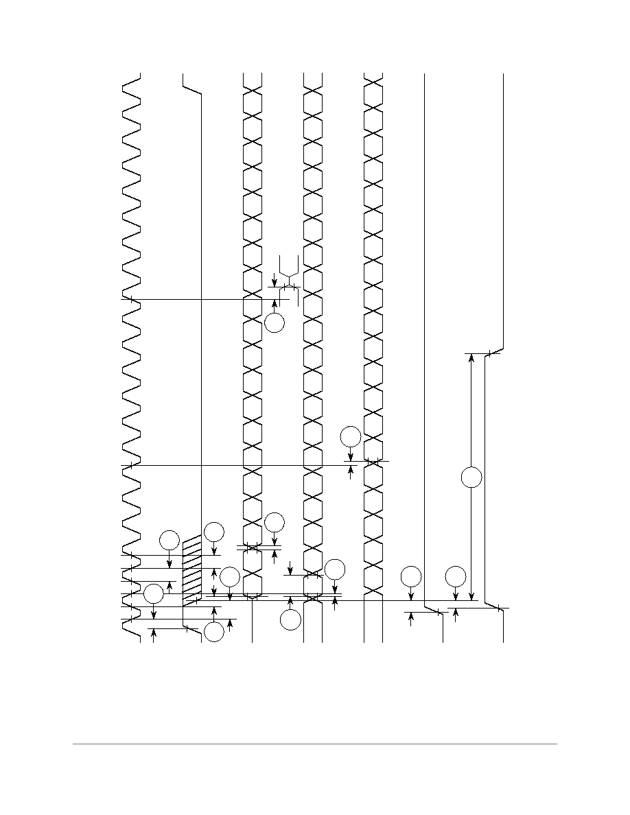
58
MPC866/859 Hardware Specifications
MOTOROLA
CPM Electrical Characteristics
CPM Electrical Characteristics
Figure 57. IDL Timing
B17
B16
B14
B13
B
1
2
B11
B10
D1
A
B27
B26
B25
B24
B23
B22
B21
B20
D2
M
B15
L1RXD
(Input)
L1TXD
(Output)
L1ST(4-1)
(Output)
L1RQ
(Output)
73
77
123456789
10
11
12
13
14
15
16
17
18
19
20
74
80
B17
B16
B15
B14
B13
B
1
2
B11
B10
D1
A
B27
B
2
6
B25
B24
B23
B22
B21
B20
D2
M
71
71
L1GR
(Input)
78
85
72
76
87
86
L1RSYNC
(Input)
L1RCLK
(Input)
81
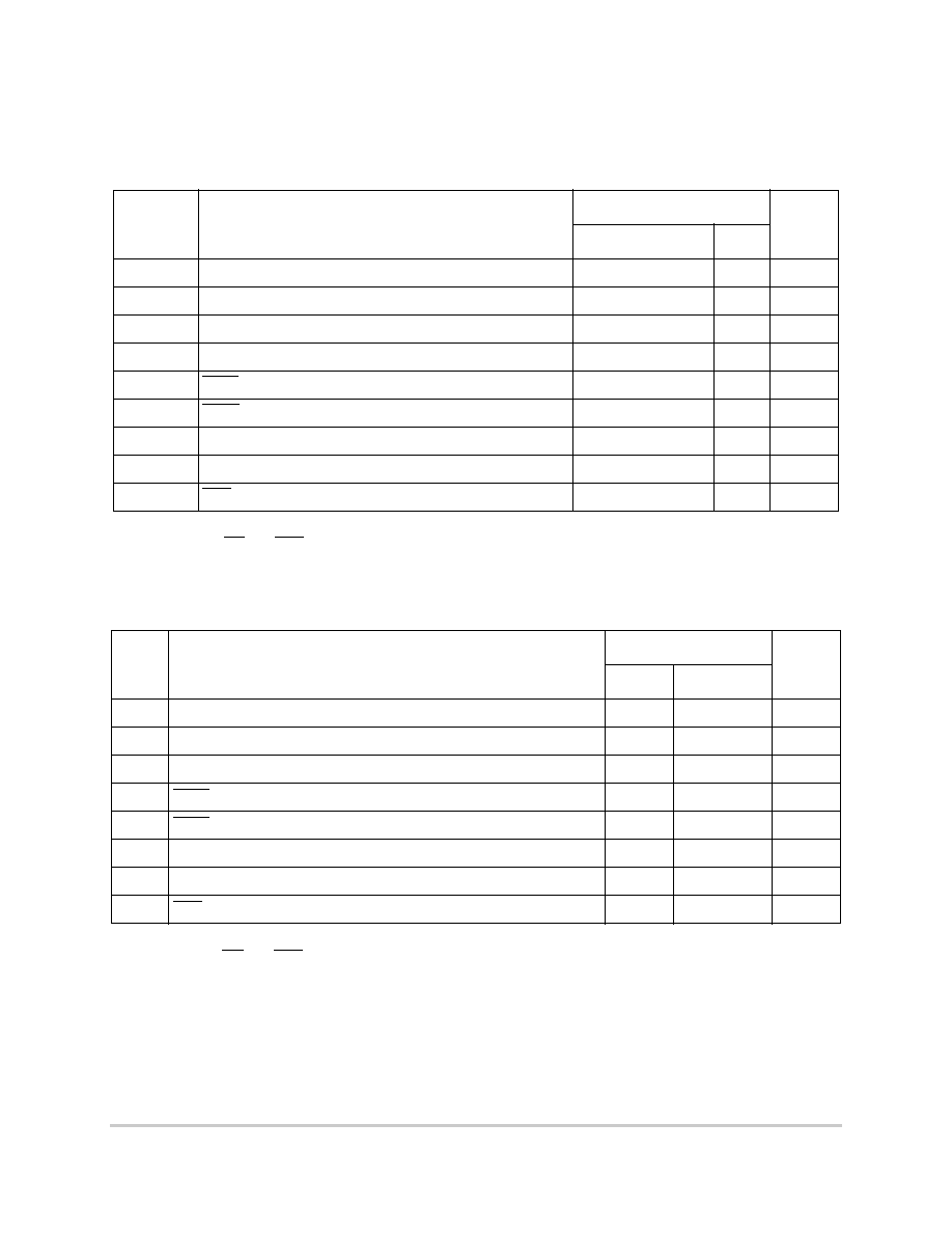
MOTOROLA
MPC866/859 Hardware Specifications
59
CPM Electrical Characteristics
12.7
SCC in NMSI Mode Electrical Specifications
Table 22 shows the NMSI external clock timings.
Table 23 shows the NMSI internal clock timings.
Table 22. NMSI External Clock Timings
Num
Characteristic
All Frequencies
Unit
Min
Max
100
RCLK1 and TCLK1 width high
1
1
The ratios SyncCLK/RCLK1 and SyncCLK/TCLK1 must be greater than or equal to 2.25/1.
1/SYNCCLK
--
ns
101
RCLK1 and TCLK1 width low
1/SYNCCLK +5
--
ns
102
RCLK1 and TCLK1 rise/fall time
--
15.00
ns
103
TXD1 active delay (from TCLK1 falling edge)
0.00
50.00
ns
104
RTS1 active/inactive delay (from TCLK1 falling edge)
0.00
50.00
ns
105
CTS1 setup time to TCLK1 rising edge
5.00
--
ns
106
RXD1 setup time to RCLK1 rising edge
5.00
--
ns
107
RXD1 hold time from RCLK1 rising edge
2
2
Also applies to CD and CTS hold time when they are used as an external sync signal.
5.00
--
ns
108 CD1 setup time to RCLK1 rising edge
5.00
--
ns
Table 23. NMSI Internal Clock Timings
Num
Characteristic
All Frequencies
Unit
Min
Max
100
RCLK1 and TCLK1 frequency
1
1
The ratios SyncCLK/RCLK1 and SyncCLK/TCLK1 must be greater or equal to 3/1.
0.00
SYNCCLK/3
MHz
102
RCLK1 and TCLK1 rise/fall time
--
--
ns
103
TXD1 active delay (from TCLK1 falling edge)
0.00
30.00
ns
104
RTS1 active/inactive delay (from TCLK1 falling edge)
0.00
30.00
ns
105
CTS1 setup time to TCLK1 rising edge
40.00
--
ns
106
RXD1 setup time to RCLK1 rising edge
40.00
--
ns
107
RXD1 hold time from RCLK1 rising edge
2
2
Also applies to CD and CTS hold time when they are used as an external sync signals.
0.00
--
ns
108
CD1 setup time to RCLK1 rising edge
40.00
--
ns
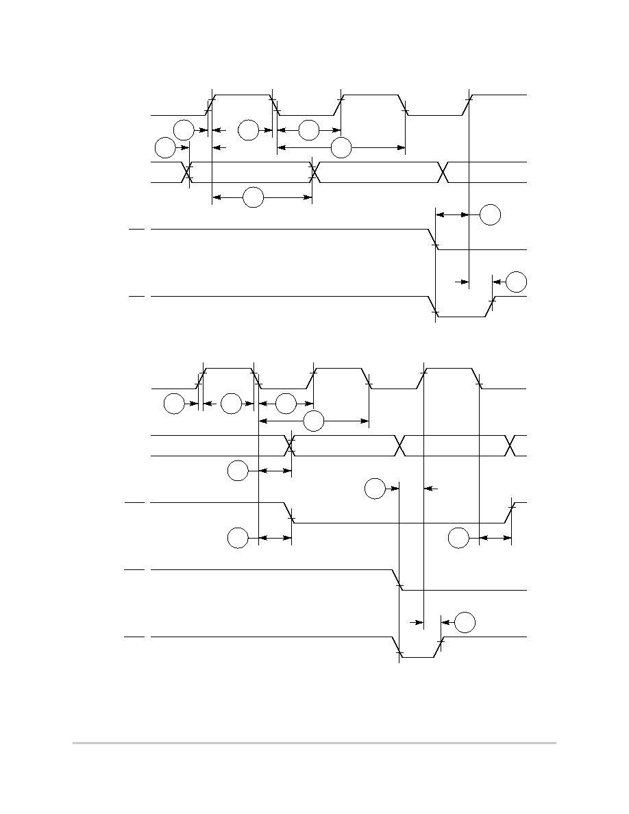
60
MPC866/859 Hardware Specifications
MOTOROLA
CPM Electrical Characteristics
CPM Electrical Characteristics
Figure 58 through Figure 60 show the NMSI timings.
Figure 58. SCC NMSI Receive Timing Diagram
Figure 59. SCC NMSI Transmit Timing Diagram
RCLK1
CD1
(Input)
102
100
107
108
107
RxD1
(Input)
CD1
(SYNC Input)
102
101
106
TCLK1
CTS1
(Input)
102
100
104
107
TxD1
(Output)
CTS1
(SYNC Input)
102
101
RTS1
(Output)
105
103
104
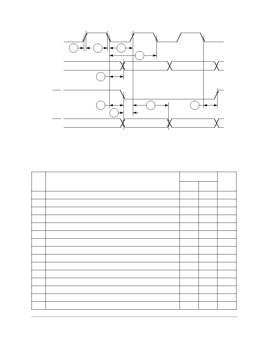
MOTOROLA
MPC866/859 Hardware Specifications
61
CPM Electrical Characteristics
Figure 60. HDLC Bus Timing Diagram
12.8
Ethernet Electrical Specifications
Table 24 shows the Ethernet timings as shown in Figure 61 through Figure 65.
Table 24. Ethernet Timing
Num
Characteristic
All Frequencies
Unit
Min
Max
120
CLSN width high
40
--
ns
121
RCLK1 rise/fall time
--
15
ns
122
RCLK1 width low
40
--
ns
123
RCLK1 clock period
1
80
120
ns
124
RXD1 setup time
20
--
ns
125
RXD1 hold time
5
--
ns
126
RENA active delay (from RCLK1 rising edge of the last data bit)
10
--
ns
127
RENA width low
100
--
ns
128
TCLK1 rise/fall time
--
15
ns
129
TCLK1 width low
40
--
ns
130
TCLK1 clock period
1
99
101
ns
131
TXD1 active delay (from TCLK1 rising edge)
--
50
ns
132
TXD1 inactive delay (from TCLK1 rising edge)
6.5
50
ns
133
TENA active delay (from TCLK1 rising edge)
10
50
ns
134
TENA inactive delay (from TCLK1 rising edge)
10
50
ns
TCLK1
CTS1
(Echo Input)
102
100
104
TxD1
(Output)
102
101
RTS1
(Output)
103
104
107
105
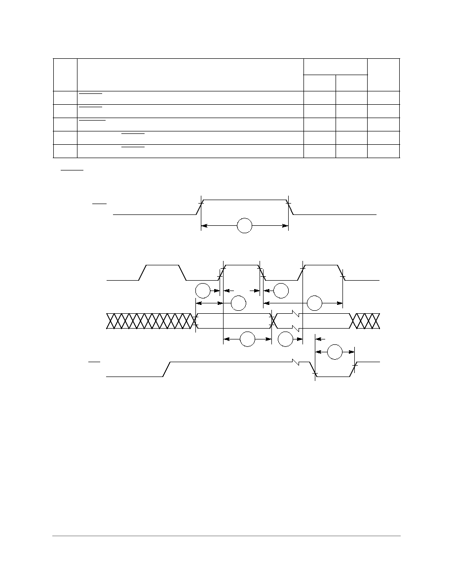
62
MPC866/859 Hardware Specifications
MOTOROLA
CPM Electrical Characteristics
CPM Electrical Characteristics
Figure 61. Ethernet Collision Timing Diagram
Figure 62. Ethernet Receive Timing Diagram
135
RSTRT active delay (from TCLK1 falling edge)
10
50
ns
136
RSTRT inactive delay (from TCLK1 falling edge)
10
50
ns
137
REJECT width low
1
--
CLK
138
CLKO1 low to SDACK asserted
2
--
20
ns
139
CLKO1 low to SDACK negated
2
--
20
ns
1
The ratios SyncCLK/RCLK1 and SyncCLK/TCLK1 must be greater or equal to 2/1.
2
SDACK is asserted whenever the SDMA writes the incoming frame DA into memory.
Table 24. Ethernet Timing (continued)
Num
Characteristic
All Frequencies
Unit
Min
Max
CLSN(CTS1)
120
(Input)
RCLK1
121
RxD1
(Input)
121
RENA(CD1)
(Input)
125
124
123
127
126
Last Bit
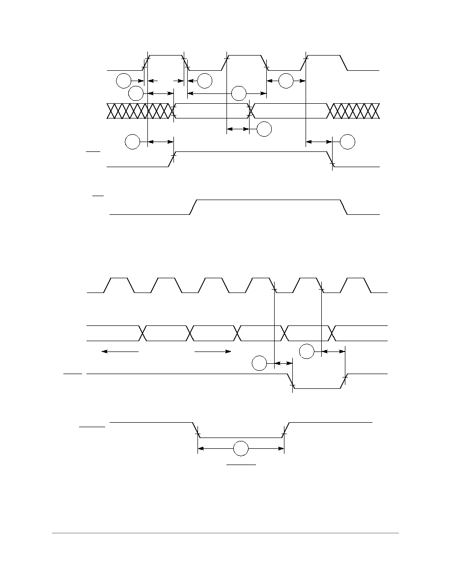
MOTOROLA
MPC866/859 Hardware Specifications
63
CPM Electrical Characteristics
Figure 63. Ethernet Transmit Timing Diagram
Figure 64. CAM Interface Receive Start Timing Diagram
Figure 65. CAM Interface REJECT Timing Diagram
TCLK1
128
TxD1
(Output)
128
TENA(RTS1)
(Input)
Notes:
Transmit clock invert (TCI) bit in GSMR is set.
If RENA is deasserted before TENA, or RENA is not asserted at all during transmit, then the
CSL bit is set in the buffer descriptor at the end of the frame transmission.
1.
2.
RENA(CD1)
(Input)
133
134
132
131
121
129
RCLK1
RxD1
(Input)
RSTRT
(Output)
0
136
125
1
1
BIT1
BIT2
Start Frame Delimiter
REJECT
137
64
MPC866/859 Hardware Specifications
MOTOROLA
CPM Electrical Characteristics
CPM Electrical Characteristics
12.9
SMC Transparent AC Electrical Specifications
Table 25 shows the SMC transparent timings as shown in Figure 66.
Figure 66. SMC Transparent Timing Diagram
Table 25. SMC Transparent Timing
Num
Characteristic
All Frequencies
Unit
Min
Max
150
SMCLK clock period
1
1
Sync CLK must be at least twice as fast as SMCLK.
100
--
ns
151
SMCLK width low
50
--
ns
151A
SMCLK width high
50
--
ns
152
SMCLK rise/fall time
--
15
ns
153
SMTXD active delay (from SMCLK falling edge)
10
50
ns
154
SMRXD/SMSYNC setup time
20
--
ns
155
RXD1/SMSYNC hold time
5
--
ns
SMCLK
SMRXD
(Input)
152
150
SMTXD
(Output)
152
151
SMSYNC
151A
154
153
155
154
155
NOTE 1
NOTE:
This delay is equal to an integer number of character-length clocks.
1.

MOTOROLA
MPC866/859 Hardware Specifications
65
CPM Electrical Characteristics
12.10 SPI Master AC Electrical Specifications
Table 26 shows the SPI master timings as shown in Figure 67 and Figure 68.
Figure 67. SPI Master (CP = 0) Timing Diagram
Table 26. SPI Master Timing
Num
Characteristic
All Frequencies
Unit
Min
Max
160
MASTER cycle time
4
1024
t
cyc
161
MASTER clock (SCK) high or low time
2
512
t
cyc
162
MASTER data setup time (inputs)
15
--
ns
163
Master data hold time (inputs)
0
--
ns
164
Master data valid (after SCK edge)
--
10
ns
165
Master data hold time (outputs)
0
--
ns
166
Rise time output
--
15
ns
167
Fall time output
--
15
ns
SPIMOSI
(Output)
SPICLK
(CI=0)
(Output)
SPICLK
(CI=1)
(Output)
SPIMISO
(Input)
162
Data
166
167
161
161
160
msb
lsb
msb
msb
Data
lsb
msb
167
166
163
166
167
165
164
66
MPC866/859 Hardware Specifications
MOTOROLA
CPM Electrical Characteristics
CPM Electrical Characteristics
Figure 68. SPI Master (CP = 1) Timing Diagram
12.11 SPI Slave AC Electrical Specifications
Table 27 shows the SPI slave timings as shown in Figure 69 and Figure 70.
Table 27. SPI Slave Timing
Num
Characteristic
All Frequencies
Unit
Min
Max
170
Slave cycle time
2
--
t
cyc
171
Slave enable lead time
15
--
ns
172
Slave enable lag time
15
--
ns
173
Slave clock (SPICLK) high or low time
1
--
t
cyc
174
Slave sequential transfer delay (does not require deselect)
1
--
t
cyc
175
Slave data setup time (inputs)
20
--
ns
176
Slave data hold time (inputs)
20
--
ns
177
Slave access time
--
50
ns
SPIMOSI
(Output)
SPICLK
(CI=0)
(Output)
SPICLK
(CI=1)
(Output)
SPIMISO
(Input)
Data
166
167
161
161
160
msb
lsb
msb
msb
Data
lsb
msb
167
166
163
166
167
165
164
162
MOTOROLA
MPC866/859 Hardware Specifications
67
CPM Electrical Characteristics
Figure 69. SPI Slave (CP = 0) Timing Diagram
Figure 70. SPI Slave (CP = 1) Timing Diagram
SPIMOSI
(Input)
SPICLK
(CI=0)
(Input)
SPICLK
(CI=1)
(Input)
SPIMISO
(Output)
180
Data
181
182
173
173
170
msb
lsb
msb
181
177
182
175
179
SPISEL
(Input)
171
172
174
Data
msb
lsb
msb
Undef
181
178
176
182
SPIMOSI
(Input)
SPICLK
(CI=0)
(Input)
SPICLK
(CI=1)
(Input)
SPIMISO
(Output)
180
Data
181
182
msb
lsb
181
177
182
175
179
SPISEL
(Input)
174
Data
msb
lsb
Undef
178
176
182
msb
msb
172
173
173
171
170
181
68
MPC866/859 Hardware Specifications
MOTOROLA
CPM Electrical Characteristics
CPM Electrical Characteristics
12.12 I
2
C AC Electrical Specifications
Table 28 shows the I
2
C (SCL < 100 kHz) timings.
Table 28. I
2
C Timing (SCL < 100 kHz)
Num
Characteristic
All Frequencies
Unit
Min
Max
200
SCL clock frequency (slave)
0
100
kHz
200
SCL clock frequency (master)
1
1
SCL frequency is given by SCL = BRGCLK_frequency / ((BRG register + 3) * pre_scaler * 2).
The ratio SyncClk/(BRGCLK/pre_scaler) must be greater or equal to 4/1.
1.5
100
kHz
202
Bus free time between transmissions
4.7
--
µs
203
Low period of SCL
4.7
--
µs
204
High period of SCL
4.0
--
µs
205
Start condition setup time
4.7
--
µs
206
Start condition hold time
4.0
--
µs
207
Data hold time
0
--
µs
208
Data setup time
250
--
ns
209
SDL/SCL rise time
--
1
µs
210
SDL/SCL fall time
--
300
ns
211
Stop condition setup time
4.7
--
µs
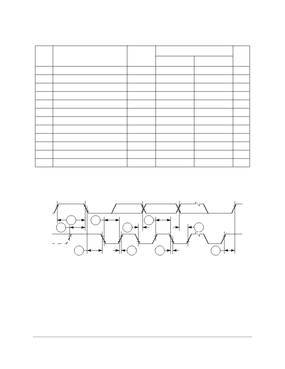
MOTOROLA
MPC866/859 Hardware Specifications
69
CPM Electrical Characteristics
Table 29 shows the I
2
C (SCL > 100 kHz) timings.
Figure 71 shows the I
2
C bus timing.
Figure 71. I
2
C Bus Timing Diagram
Table 29. I
2
C Timing (SCL > 100 kHz)
Num
Characteristic
Expression
All Frequencies
Unit
Min
Max
200
SCL clock frequency (slave)
fSCL
0
BRGCLK/48
Hz
200
SCL clock frequency (master)
1
1
SCL frequency is given by SCL = BrgClk_frequency / ((BRG register + 3) * pre_scaler * 2).
The ratio SyncClk/(Brg_Clk/pre_scaler) must be greater or equal to 4/1.
fSCL
BRGCLK/16512
BRGCLK/48
Hz
202
Bus free time between transmissions
--
1/(2.2 * fSCL)
--
s
203
Low period of SCL
--
1/(2.2 * fSCL)
--
s
204
High period of SCL
--
1/(2.2 * fSCL)
--
s
205
Start condition setup time
--
1/(2.2 * fSCL)
--
s
206
Start condition hold time
--
1/(2.2 * fSCL)
--
s
207
Data hold time
--
0
--
s
208
Data setup time
--
1/(40 * fSCL)
--
s
209
SDL/SCL rise time
--
--
1/(10 * fSCL)
s
210
SDL/SCL fall time
--
--
1/(33 * fSCL)
s
211
Stop condition setup time
--
1/2(2.2 * fSCL)
--
s
SCL
202
205
203
207
204
208
206
209
211
210
SDA
70
MPC866/859 Hardware Specifications
MOTOROLA
UTOPIA AC Electrical Specifications
UTOPIA AC Electrical Specifications
13
UTOPIA AC Electrical Specifications
Table 30 through Table 32 show the AC electrical specifications for the UTOPIA interface.
Table 30. UTOPIA Master (Muxed Mode) Electrical Specifications
Num
Signal Characteristic
Direction
Min
Max
Unit
U1
UtpClk rise/fall time (Internal clock option)
Output
--
4
ns
Duty cycle
50
50
%
Frequency
--
33
MHz
U2
UTPB, SOC, RxEnb, TxEnb, RxAddr, and TxAddr-active
delay (and PHREQ and PHSEL active delay in MPHY mode)
Output
2
16
ns
U3
UTPB, SOC, Rxclav and Txclav setup time
Input
4
--
ns
U4
UTPB, SOC, Rxclav and Txclav hold time
Input
1
--
ns
Table 31. UTOPIA Master (Split Bus Mode) Electrical Specifications
Num
Signal Characteristic
Direction
Min
Max
Unit
U1
UtpClk rise/fall time (Internal clock option)
Output
--
4
ns
Duty cycle
50
50
%
Frequency
--
33
MHz
U2
UTPB, SOC, RxEnb, TxEnb, RxAddr and TxAddr active
delay (PHREQ and PHSEL active delay in MPHY mode)
Output
2
16
ns
U3
UTPB_Aux, SOC_Aux, Rxclav, and Txclav setup time
Input
4
--
ns
U4
UTPB_Aux, SOC_Aux, Rxclav, and Txclav hold time
Input
1
--
ns
Table 32. UTOPIA Slave (Split Bus Mode) Electrical Specifications
Num
Signal Characteristic
Direction
Min
Max
Unit
U1
UtpClk rise/fall time (external clock option)
Input
--
4
ns
Duty cycle
40
60
%
Frequency
--
33
MHz
U2
UTPB, SOC, Rxclav and Txclav active delay
Output
2
16
ns
U3
UTPB_AUX, SOC_Aux, RxEnb, TxEnb, RxAddr, and TxAddr
setup time
Input
4
--
ns
U4
UTPB_AUX, SOC_Aux, RxEnb, TxEnb, RxAddr, and TxAddr
hold time
Input
1
--
ns
MOTOROLA
MPC866/859 Hardware Specifications
71
UTOPIA AC Electrical Specifications
Figure 72 shows signal timings during UTOPIA receive operations.
Figure 72. UTOPIA Receive Timing
Figure 73 shows signal timings during UTOPIA transmit operations.
Figure 73. UTOPIA Transmit Timing
UtpClk
UTPB
RxEnb
U1
3
2
SOC
4
RxClav
PHREQn
3
4
HighZ at MPHY
HighZ at MPHY
U1
U2
U3
U4
U4
U3
U2
UtpClk
UTPB
TxEnb
1
2
SOC
5
TxClav
PHSELn
3
4
5
HighZ at MPHY
High-Z at MPHY
U1
U1
U2
U2
U2
U3
U4
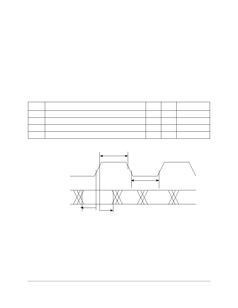
72
MPC866/859 Hardware Specifications
MOTOROLA
FEC Electrical Characteristics
FEC Electrical Characteristics
14
FEC Electrical Characteristics
This section provides the AC electrical specifications for the fast Ethernet controller (FEC). Note that the
timing specifications for the MII signals are independent of system clock frequency (part speed
designation). Also, MII signals use TTL signal levels compatible with devices operating at either 5.0 or 3.3
V.
14.1
MII Receive Signal Timing (MII_RXD [3:0], MII_RX_DV,
MII_RX_ER, MII_RX_CLK)
The receiver functions correctly up to a MII_RX_CLK maximum frequency of 25 MHz + 1%. There is no
minimum frequency requirement. In addition, the processor clock frequency must exceed the
MII_RX_CLK frequency ≠ 1%. Table 33 shows the timings for MII receive signal.
Figure 74 shows the timings for MII receive signal.
Figure 74. MII Receive Signal Timing Diagram
14.2
MII Transmit Signal Timing (MII_TXD[3:0], MII_TX_EN,
MII_TX_ER, MII_TX_CLK)
The transmitter functions correctly up to a MII_TX_CLK maximum frequency of 25 MHz +1%. There is
no minimum frequency requirement. In addition, the processor clock frequency must exceed the
MII_TX_CLK frequency - 1%.
Table 33. MII Receive Signal Timing
Num
Characteristic
Min
Max
Unit
M1
MII_RXD[3:0], MII_RX_DV, MII_RX_ER to MII_RX_CLK setup
5
--
ns
M2
MII_RX_CLK to MII_RXD[3:0], MII_RX_DV, MII_RX_ER hold
5
--
ns
M3
MII_RX_CLK pulse width high
35%
65%
MII_RX_CLK period
M4
MII_RX_CLK pulse width low
35%
65%
MII_RX_CLK period
M1
M2
MII_RX_CLK (input)
MII_RXD[3:0] (inputs)
MII_RX_DV
MII_RX_ER
M3
M4
MOTOROLA
MPC866/859 Hardware Specifications
73
FEC Electrical Characteristics
Table 34 shows information on the MII transmit signal timing.
Figure 75 shows the MII transmit signal timing diagram.
Figure 75. MII Transmit Signal Timing Diagram
14.3
MII Async Inputs Signal Timing (MII_CRS, MII_COL)
Table 35 shows the timing for on the MII async inputs signal.
Figure 76 shows the MII asynchronous inputs signal timing diagram.
Figure 76. MII Async Inputs Timing Diagram
Table 34. MII Transmit Signal Timing
Num
Characteristic
Min
Max
Unit
M5
MII_TX_CLK to MII_TXD[3:0], MII_TX_EN, MII_TX_ER
invalid
5
--
ns
M6
MII_TX_CLK to MII_TXD[3:0], MII_TX_EN, MII_TX_ER
valid
--
25
--
M7
MII_TX_CLK pulse width high
35%
65%
MII_TX_CLK period
M8
MII_TX_CLK pulse width low
35%
65%
MII_TX_CLK period
Table 35. MII Async Inputs Signal Timing
Num
Characteristic
Min
Max
Unit
M9
MII_CRS, MII_COL minimum pulse width
1.5
--
MII_TX_CLK period
M6
MII_TX_CLK (input)
MII_TXD[3:0] (outputs)
MII_TX_EN
MII_TX_ER
M5
M7
M8
MII_CRS, MII_COL
M9
74
MPC866/859 Hardware Specifications
MOTOROLA
FEC Electrical Characteristics
FEC Electrical Characteristics
14.4
MII Serial Management Channel Timing (MII_MDIO,
MII_MDC)
Table 36 shows the timing for the MII serial management channel signal. The FEC functions correctly with
a maximum MDC frequency in excess of 2.5 MHz. The exact upper bound is under investigation.
Figure 77 shows the MII serial management channel timing diagram.
Figure 77. MII Serial Management Channel Timing Diagram
Table 36. MII Serial Management Channel Timing
Num
Characteristic
Min
Max
Unit
M10
MII_MDC falling edge to MII_MDIO output invalid (minimum
propagation delay)
0
--
ns
M11
MII_MDC falling edge to MII_MDIO output valid (maximum
propagation delay)
--
25
ns
M12
MII_MDIO (input) to MII_MDC rising edge setup
10
--
ns
M13
MII_MDIO (input) to MII_MDC rising edge hold
0
--
ns
M14
MII_MDC pulse width high
40%
60%
MII_MDC period
M15
MII_MDC pulse width low
40%
60%
MII_MDC period
M11
MII_MDC (output)
MII_MDIO (output)
M12
M13
MII_MDIO (input)
M10
M14
MM15
MOTOROLA
MPC866/859 Hardware Specifications
75
Mechanical Data and Ordering Information
15
Mechanical Data and Ordering Information
Table 37 shows information on the MPC866/859 derivative devices.
Table 38 identifies the packages and operating frequencies orderable for the MPC866/859 derivative
devices.
Table 37. MPC866/859 Derivatives
Device
Number
of
SCCs
1
1
Serial communications controller (SCC).
Ethernet
Support
Multi-Channel
HDLC Support
ATM Support
Cache Size
Instruction
Data
MPC866T
4
10/100 Mbps
Yes
Yes
4 Kbyte
4 Kbytes
MPC866P
4
10/100 Mbps
Yes
Yes
16 Kbyte
8 Kbytes
MPC859T
1 (SCC1)
10/100 Mbps
Yes
Yes
4 Kbyte
4 Kbytes
MPC859DSL
1 (SCC1)
10/100 Mbps
No
Up to 4 addresses
4 Kbyte
4 Kbytes
Table 38. MPC866/859 Package/Frequency Orderable
Package Type
Temperature (Tj)
Frequency (MHz)
Order Number
Plastic ball grid array
(ZP suffix)
0∞ to 95∞C
50
MPC859DSLZP50
66
MPC859DSLZP66
100
MPC866PZP100
MPC866TZP100
MPC859PZP100
MPC859TZP100
133
MPC866PZP133
MPC866TZP133
MPC859PZP133
MPC859TZP133
Plastic ball grid array
(CZP suffix)
≠40∞ to 100∞C
TBD
1
1
Additional extended temperature devices can be made available at 50, 66, 80, and100MHz.
TBD
76
MPC866/859 Hardware Specifications
MOTOROLA
Mechanical Data and Ordering Information
Mechanical Data and Ordering Information
15.1
Pin Assignments
Figure 78 shows the top view pinout of the PBGA package. For additional information, see the MPC866
PowerQUICC Family User's Manual.
NOTE: This is the top view of the device.
Figure 78. Pinout of the PBGA Package
PD3
IRQ7
D0
D4
D1
D2
D3
D5
VDDL
D6
D7
D29
CLKOUT IPA3
DP2
A2
A7
A14
A27
A29
A30
A28
A31
VDDL BSA2
WE1
WE3
CE2A
CS1
CS4
A5
A11
18
16
14
13
12
11
10
9
8
7
6
5
3
2
4
17
15
1
19
A1
A6
A13
A17
A21
A23
A22
TSIZ0 BSA3 M_CRS WE2 GPLA2
CE1A
WR
CS5
A4
A10
GPLB4
A0
PA15
A3
A12
A16
A20
A24
A26
TSIZ1 BSA1
WE0 GPLA1 GPLA3
CS0
TA
CS7
PB31
A9
GPLA4
PB30
PC14
PC15
N/C
N/C
A15
A19
A25
A18
BSA0 GPLA0
N/C
CS6
GPLA5 BDIP
CS2
PA14
A8
TEA
PB28
PC13
PB29
VDDH
VDDH
BI
BG
CS3
PA13
BB
PB27
PC12
VDDL
GND
GND
TS
IRQ3
VDDL
PA12
BURST
PB26
TMS
PA11
IRQ6
IPB4
BR
TDO
IPB3
TRST
M_MDIO
TCK
IRQ2
IPB0
M_COL
TDI
IPB7
VDDL
PB24
PB25
IPB1
IPB2
IPB5
PA10
ALEB
PC11
PA9
PB21
GND
IPB6 ALEA
BADDR30
PB23
IRQ4
PC10
PC9
PB20
AS
OP1
OP0
PA8
MODCK1
PB22
PC8
PC7
BADDR28
BADDR29
MODCK2
PA6
VDDL
PA7
PA5
PB16
TEXP
EXTCLK
HRESET
PB18
EXTAL
PB19
PB17
VDDL
GND
RSTCONF SRESET
VDDL
PA3
GND
XTAL
PA4
PA2
PD12
VDDH
WAIT_A
PORESET
WAIT_B
PB15
VDDH
VDDL
PC6
PC5
PD11
VDDH D12
D17
D9
D15
D22
D25
D31
IPA6
IPA0
IPA7
N/C
IPA1
PC4
PD7
VDDSYN
PA1
PB14
PD4
IRQ1
D8
D23
D11
D16
D19
D21
D26
D30
IPA5
IPA2
N/C
IPA4
PD15
PD5
VSSSYN
PA0
PD13
PD6
IRQ0 D13
D27
D10
D14
D18
D20
D24
D28
DP1
DP0
N/C
DP3
PD9
M_Tx_EN
VSSSYN1
PD14
B
A
C
D
E
F
G
H
J
K
L
M
N
P
R
T
U
V
W
PD10
PD8
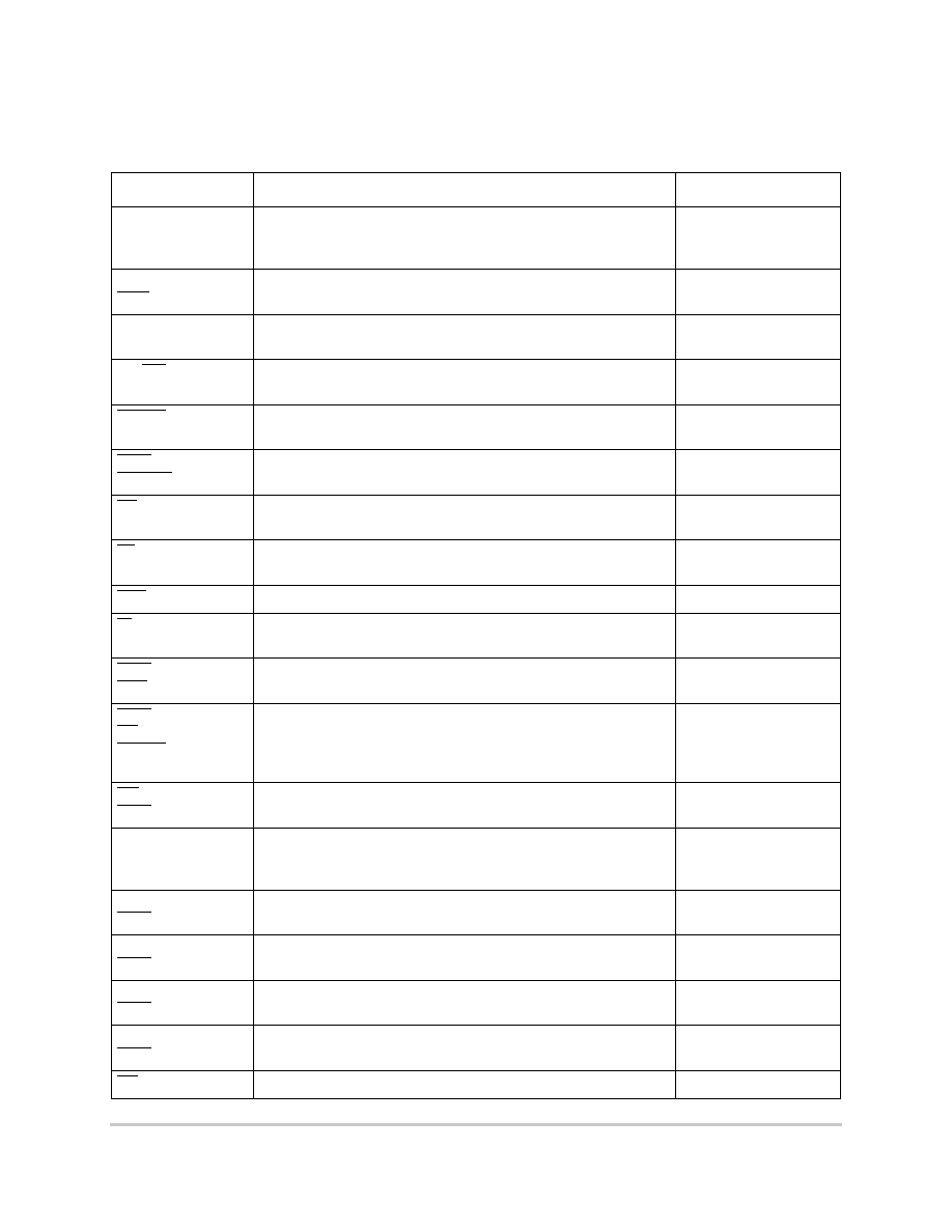
MOTOROLA
MPC866/859 Hardware Specifications
77
Mechanical Data and Ordering Information
Table 39 contains a list of the MPC866 input and output signals and shows multiplexing and pin
assignments.
Table 39. Pin Assignments
Name
Pin Number
Type
A[0:31]
B19, B18, A18, C16, B17, A17, B16, A16, D15, C15, B15, A15,
C14, B14, A14, D12, C13, B13, D9, D11, C12, B12, B10, B11, C11,
D10, C10, A13, A10, A12, A11, A9
Bidirectional
Three-state
TSIZ0
REG
B9
Bidirectional
Three-state
TSIZ1
C9
Bidirectional
Three-state
RD/WR B2
Bidirectional
Three-state
BURST
F1
Bidirectional
Three-state
BDIP
GPL_B5
D2
Output
TS
F3
Bidirectional
Active Pull-up
TA
C2
Bidirectional
Active Pull-up
TEA
D1
Open-drain
BI
E3
Bidirectional
Active Pull-up
IRQ2
RSV
H3
Bidirectional
Three-state
IRQ4
KR
RETRY
SPKROUT
K1
Bidirectional
Three-state
CR
IRQ3
F2
Input
D[0:31]
W14, W12, W11, W10, W13, W9, W7, W6, U13, T11, V11, U11,
T13, V13, V10, T10, U10, T12, V9, U9, V8, U8, T9, U12, V7, T8, U7,
V12, V6, W5, U6, T7
Bidirectional
Three-state
DP0
IRQ3
V3
Bidirectional
Three-state
DP1
IRQ4
V5
Bidirectional
Three-state
DP2
IRQ5
W4
Bidirectional
Three-state
DP3
IRQ6
V4
Bidirectional
Three-state
BR
G4
Bidirectional
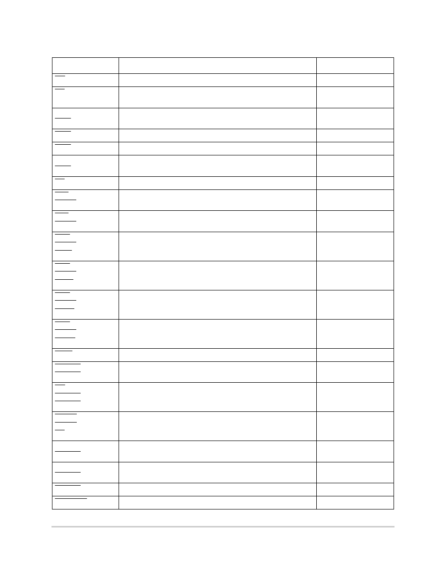
78
MPC866/859 Hardware Specifications
MOTOROLA
Mechanical Data and Ordering Information
Mechanical Data and Ordering Information
BG
E2
Bidirectional
BB
E1
Bidirectional
Active Pull-up
FRZ
IRQ6
G3
Bidirectional
IRQ0
V14
Input
IRQ1
U14
Input
M_TX_CLK
IRQ7
W15
Input
CS[0:5]
C3, A2, D4, E4, A4, B4
Output
CS6
CE1_B
D5
Output
CS7
CE2_B
C4
Output
WE0
BS_B0
IORD
C7
Output
WE1
BS_B1
IOWR
A6
Output
WE2
BS_B2
PCOE
B6
Output
WE3
BS_B3
PCWE
A5
Output
BS_A[0:3]
D8, C8, A7, B8
Output
GPL_A0
GPL_B0
D7
Output
OE
GPL_A1
GPL_B1
C6
Output
GPL_A[2:3]
GPL_B[2:3]
CS[2≠3]
B5, C5
Output
UPWAITA
GPL_A4
C1
Bidirectional
UPWAITB
GPL_B4
B1
Bidirectional
GPL_A5
D3
Output
PORESET
R2
Input
Table 39. Pin Assignments (continued)
Name
Pin Number
Type
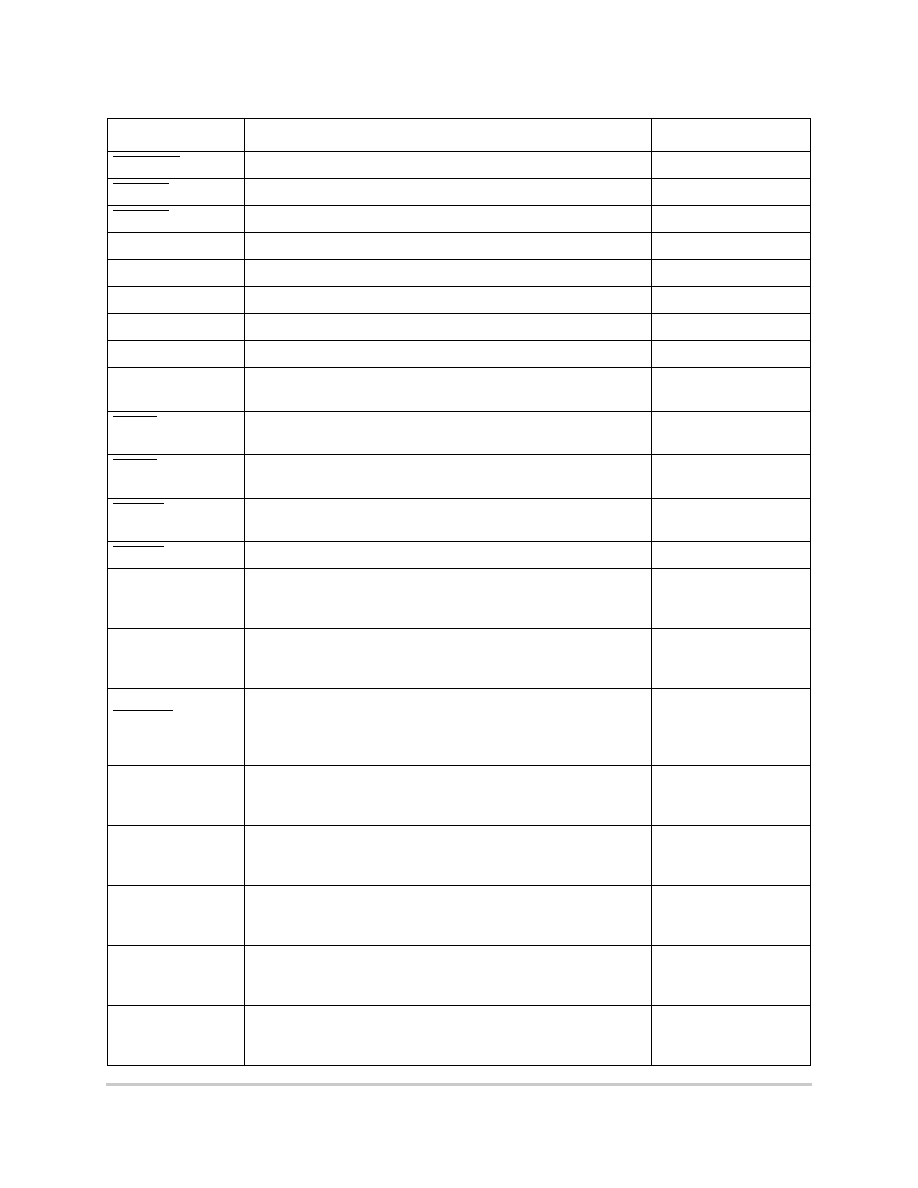
MOTOROLA
MPC866/859 Hardware Specifications
79
Mechanical Data and Ordering Information
RSTCONF
P3
Input
HRESET
N4
Open-drain
SRESET
P2
Open-drain
XTAL
P1
Analog Output
EXTAL
N1
Analog Input (3.3V only)
CLKOUT
W3
Output
EXTCLK
N2
Input (3.3V only)
TEXP
N3
Output
ALE_A
MII-TXD1
K2
Output
CE1_A
MII-TXD2
B3
Output
CE2_A
MII-TXD3
A3
Output
WAIT_A
SOC_Split
2
R3
Input
WAIT_B
R4
Input
IP_A0
UTPB_Split0
2
MII-RXD3
T5
Input
IP_A1
UTPB_Split1
2
MII-RXD2
T4
Input
IP_A2
IOIS16_A
UTPB_Split2
2
MII-RXD1
U3
Input
IP_A3
UTPB_Split3
2
MII-RXD0
W2
Input
IP_A4
UTPB_Split4
2
MII-RXCLK
U4
Input
IP_A5
UTPB_Split5
2
MII-RXERR
U5
Input
IP_A6
UTPB_Split6
2
MII-TXERR
T6
Input
IP_A7
UTPB_Split7
2
MII-RXDV
T3
Input
Table 39. Pin Assignments (continued)
Name
Pin Number
Type

80
MPC866/859 Hardware Specifications
MOTOROLA
Mechanical Data and Ordering Information
Mechanical Data and Ordering Information
ALE_B
DSCK/AT1
J1
Bidirectional
Three-state
IP_B[0:1]
IWP[0:1]
VFLS[0:1]
H2, J3
Bidirectional
IP_B2
IOIS16_B
AT2
J2
Bidirectional
Three-state
IP_B3
IWP2
VF2
G1
Bidirectional
IP_B4
LWP0
VF0
G2
Bidirectional
IP_B5
LWP1
VF1
J4
Bidirectional
IP_B6
DSDI
AT0
K3
Bidirectional
Three-state
IP_B7
PTR
AT3
H1
Bidirectional
Three-state
OP0
MII-TXD0
UtpClk_Split
2
L4
Bidirectional
OP1
L2
Output
OP2
MODCK1
STS
L1
Bidirectional
OP3
MODCK2
DSDO
M4
Bidirectional
BADDR30
REG
K4
Output
BADDR[28:29]
M3, M2
Output
AS
L3
Input
PA15
RXD1
RXD4
C18
Bidirectional
PA14
TXD1
TXD4
D17
Bidirectional
(Optional: Open-drain)
Table 39. Pin Assignments (continued)
Name
Pin Number
Type

MOTOROLA
MPC866/859 Hardware Specifications
81
Mechanical Data and Ordering Information
PA13
RXD2
E17
Bidirectional
PA12
TXD2
F17
Bidirectional
(Optional: Open-drain)
PA11
L1TXDB
RXD3
G16
Bidirectional
(Optional: Open-drain)
PA10
L1RXDB
TXD3
J17
Bidirectional
(Optional: Open-drain)
PA9
L1TXDA
RXD4
K18
Bidirectional
(Optional: Open-drain)
PA8
L1RXDA
TXD4
L17
Bidirectional
(Optional: Open-drain)
PA7
CLK1
L1RCLKA
BRGO1
TIN1
M19
Bidirectional
PA6
CLK2
TOUT1
M17
Bidirectional
PA5
CLK3
L1TCLKA
BRGO2
TIN2
N18
Bidirectional
PA4
CLK4
TOUT2
P19
Bidirectional
PA3
CLK5
BRGO3
TIN3
P17
Bidirectional
PA2
CLK6
TOUT3
L1RCLKB
R18
Bidirectional
PA1
CLK7
BRGO4
TIN4
T19
Bidirectional
Table 39. Pin Assignments (continued)
Name
Pin Number
Type
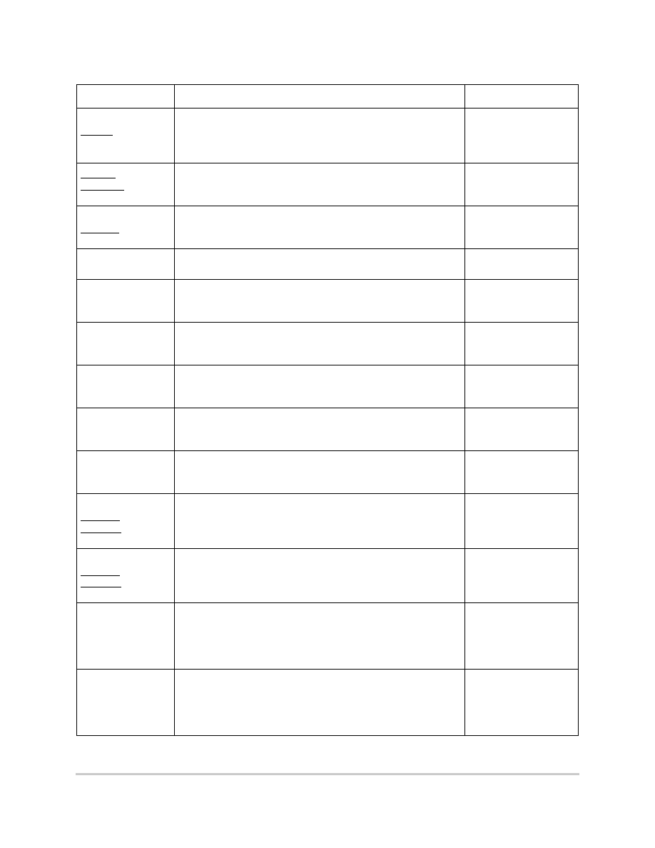
82
MPC866/859 Hardware Specifications
MOTOROLA
Mechanical Data and Ordering Information
Mechanical Data and Ordering Information
PA0
CLK8
TOUT4
L1TCLKB
U19
Bidirectional
PB31
SPISEL
REJECT1
C17
Bidirectional
(Optional: Open-drain)
PB30
SPICLK
RSTRT2
C19
Bidirectional
(Optional: Open-drain)
PB29
SPIMOSI
E16
Bidirectional
(Optional: Open-drain)
PB28
SPIMISO
BRGO4
D19
Bidirectional
(Optional: Open-drain)
PB27
I2CSDA
BRGO1
E19
Bidirectional
(Optional: Open-drain)
PB26
I2CSCL
BRGO2
F19
Bidirectional
(Optional: Open-drain)
PB25
RXADDR3
2
SMTXD1
J16
Bidirectional
(Optional: Open-drain)
PB24
TXADDR3
2
SMRXD1
J18
Bidirectional
(Optional: Open-drain)
PB23
TXADDR2
2
SDACK1
SMSYN1
K17
Bidirectional
(Optional: Open-drain)
PB22
TXADDR4
2
SDACK2
SMSYN2
L19
Bidirectional
(Optional: Open-drain)
PB21
SMTXD2
L1CLKOB
PHSEL1
1
TXADDR1
2
K16
Bidirectional
(Optional: Open-drain)
PB20
SMRXD2
L1CLKOA
PHSEL0
1
TXADDR0
2
L16
Bidirectional
(Optional: Open-drain)
Table 39. Pin Assignments (continued)
Name
Pin Number
Type
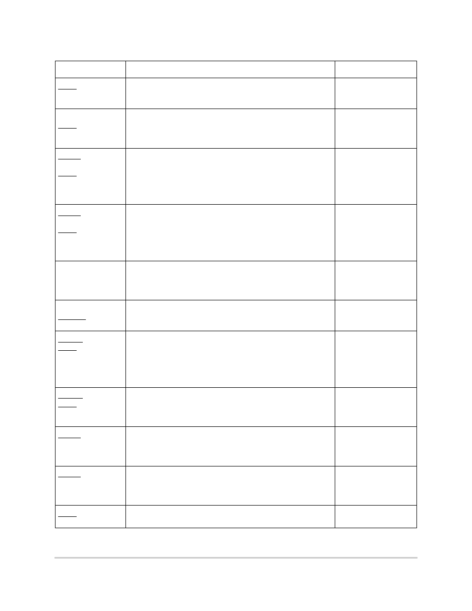
MOTOROLA
MPC866/859 Hardware Specifications
83
Mechanical Data and Ordering Information
PB19
RTS1
L1ST1
N19
Bidirectional
(Optional: Open-drain)
PB18
RXADDR4
2
RTS2
L1ST2
N17
Bidirectional
(Optional: Open-drain)
PB17
L1RQb
L1ST3
RTS3
PHREQ1
1
RXADDR1
2
P18
Bidirectional
(Optional: Open-drain)
PB16
L1RQa
L1ST4
RTS4
PHREQ0
1
RXADDR0
2
N16
Bidirectional
(Optional: Open-drain)
PB15
BRGO3
TxClav
RxClav
R17
Bidirectional
PB14
RXADDR2
2
RSTRT1
U18
Bidirectional
PC15
DREQ0
RTS1
L1ST1
RxClav
TxClav
D16
Bidirectional
PC14
DREQ1
RTS2
L1ST2
D18
Bidirectional
PC13
L1RQb
L1ST3
RTS3
E18
Bidirectional
PC12
L1RQa
L1ST4
RTS4
F18
Bidirectional
PC11
CTS1
J19
Bidirectional
Table 39. Pin Assignments (continued)
Name
Pin Number
Type
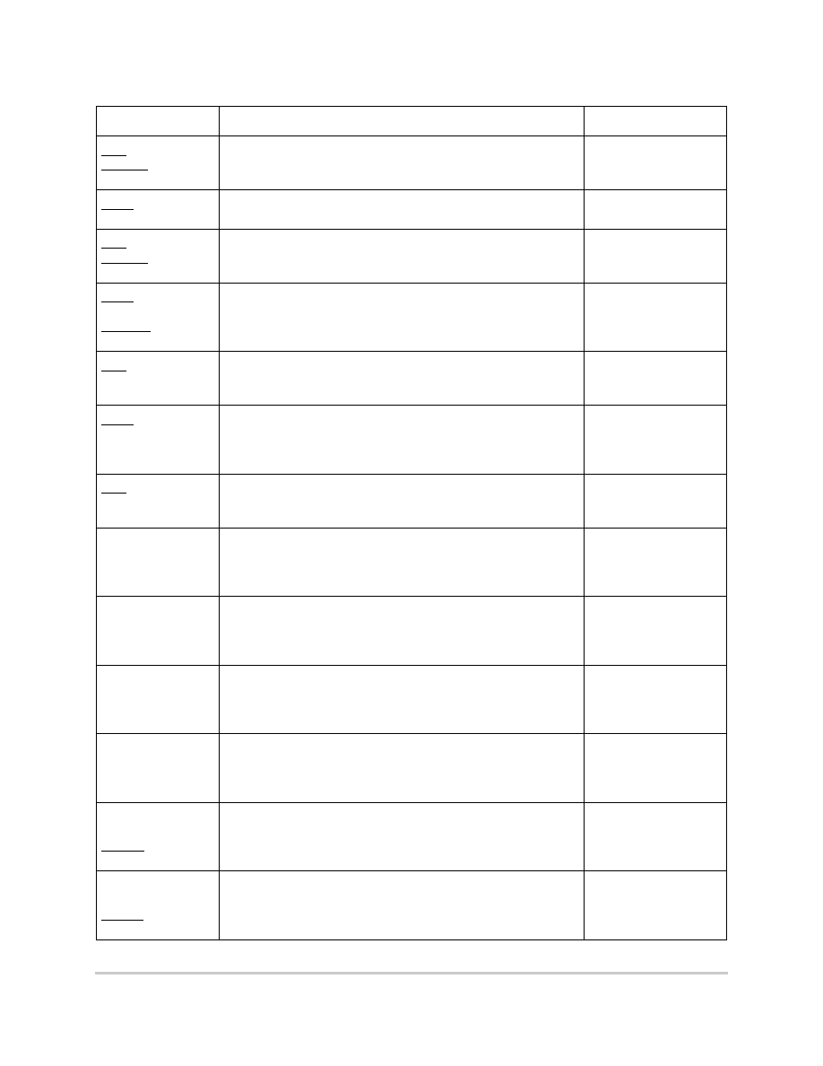
84
MPC866/859 Hardware Specifications
MOTOROLA
Mechanical Data and Ordering Information
Mechanical Data and Ordering Information
PC10
CD1
TGATE1
K19
Bidirectional
PC9
CTS2
L18
Bidirectional
PC8
CD2
TGATE2
M18
Bidirectional
PC7
CTS3
L1TSYNCB
SDACK2
M16
Bidirectional
PC6
CD3
L1RSYNCB
R19
Bidirectional
PC5
CTS4
L1TSYNCA
SDACK1
T18
Bidirectional
PC4
CD4
L1RSYNCA
T17
Bidirectional
PD15
L1TSYNCA
MII-RXD3
UTPB0
U17
Bidirectional
PD14
L1RSYNCA
MII-RXD2
UTPB1
V19
Bidirectional
PD13
L1TSYNCB
MII-RXD1
UTPB2
V18
Bidirectional
PD12
L1RSYNCB
MII-MDC
UTPB3
R16
Bidirectional
PD11
RXD3
MII-TXERR
RXENB
T16
Bidirectional
PD10
TXD3
MII-RXD0
TXENB
W18
Bidirectional
Table 39. Pin Assignments (continued)
Name
Pin Number
Type
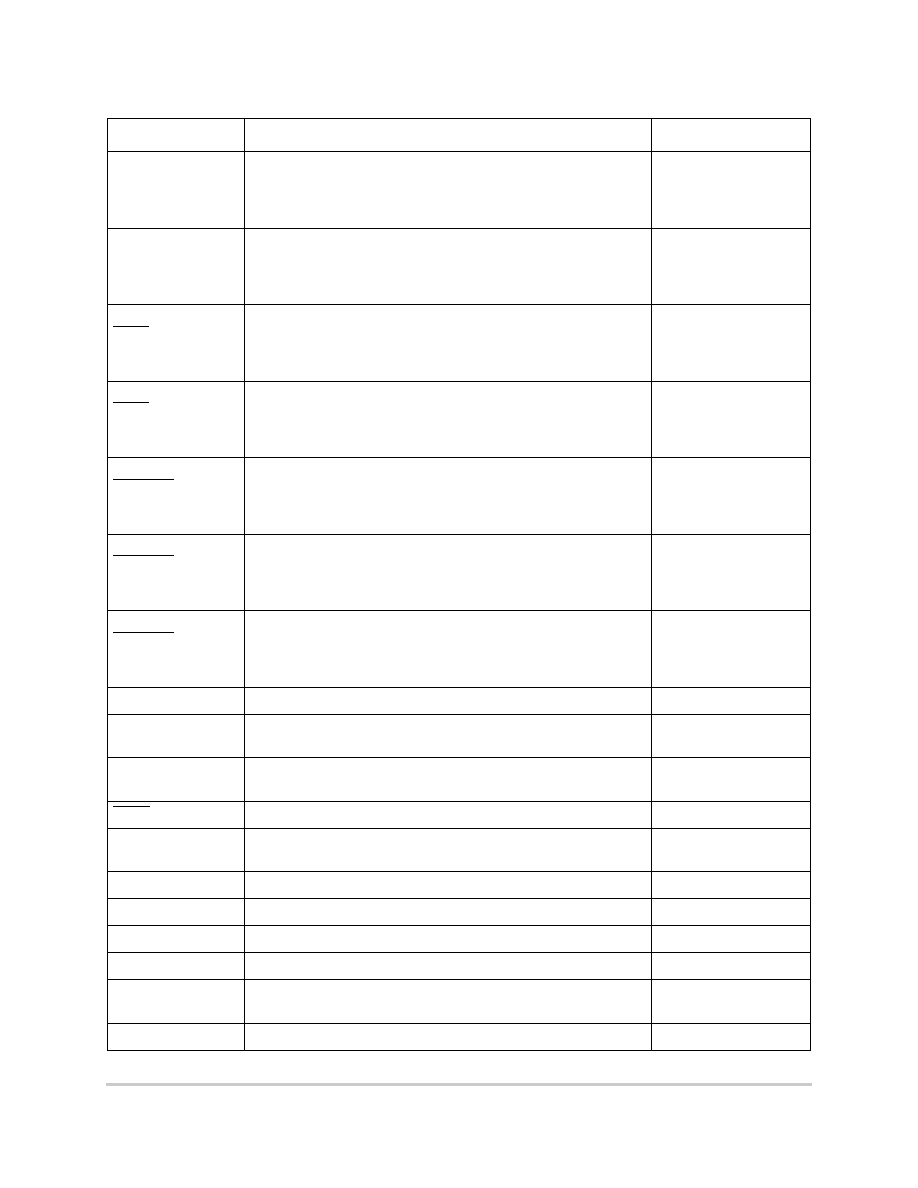
MOTOROLA
MPC866/859 Hardware Specifications
85
Mechanical Data and Ordering Information
PD9
RXD4
MII-TXD0
UTPCLK
V17
Bidirectional
PD8
TXD4
MII-MDC
MII-RXCLK
W17
Bidirectional
PD7
RTS3
MII-RXERR
UTPB4
T15
Bidirectional
PD6
RTS4
MII-RXDV
UTPB5
V16
Bidirectional
PD5
REJECT2
MII-TXD3
UTPB6
U15
Bidirectional
PD4
REJECT3
MII-TXD2
UTPB7
U16
Bidirectional
PD3
REJECT4
MII-TXD1
SOC
W16
Bidirectional
TMS
G18
Input
TDI
DSDI
H17
Input
TCK
DSCK
H16
Input
TRST
G19
Input
TDO
DSDO
G17
Output
MII_CRS
B7
Input
MII_MDIO
H18
Bidirectional
MII_TXEN
V15
Output
MII_COL
H4
Input
VSSSYN1
V1
PLL analog VDD and
GND
VSSSYN
U1
Power
Table 39. Pin Assignments (continued)
Name
Pin Number
Type
86
MPC866/859 Hardware Specifications
MOTOROLA
Mechanical Data and Ordering Information
Mechanical Data and Ordering Information
15.2
Mechanical Dimensions of the PBGA Package
For more information on the printed-circuit board layout of the PBGA package, including thermal via
design and suggested pad layout, please refer to Plastic Ball Grid Array Application Note (order number:
AN1231/D) available from your local Motorola sales office. Figure 79 shows the mechanical dimensions of
the PBGA package.
VDDSYN
T1
Power
GND
F6, F7, F8, F9, F10, F11, F12, F13, F14, G6, G7, G8, G9, G10,
G11, G12, G13, G14, H6, H7, H8, H9, H10, H11, H12, H13, H14,
J6, J7, J8, J9, J10, J11, J12, J13, J14, K6, K7, K8, K9, K10, K11,
K12, K13, K14, L6, L7, L8, L9, L10, L11, L12, L13, L14, M6, M7,
M8, M9, M10, M11, M12, M13, M14, N6, N7, N8, N9, N10, N11,
N12, N13, N14, P6, P7, P8, P9, P10, P11, P12, P13, P14
Power
VDDL
A8, M1, W8, H19, F4, F16, P4, P16, R1
Power
VDDH
E5, E6, E7, E8, E9, E10, E11, E12, E13, E14, E15, F5, F15, G5,
G15, H5, H15, J5, J15, K5, K15, L5, L15, M5, M15, N5, N15, P5,
P15, R5, R6, R7, R8, R9, R10, R11, R12, R13, R14, R15, T14
Power
N/C
D6, D13, D14, U2, V2, T2
No-connect
1
Classic SAR mode only
2
ESAR mode only
Table 39. Pin Assignments (continued)
Name
Pin Number
Type

MOTOROLA
MPC866/859 Hardware Specifications
87
Mechanical Data and Ordering Information
Figure 79. Mechanical Dimensions and Bottom Surface Nomenclature of the PBGA Package
Note:
Solder sphere composition for MPC866XZP, MPC859PZP, MPC859DSLZP, and MPC859TZP
is 62%Sn 36%Pb 2%Ag

88
MPC866/859 Hardware Specifications
MOTOROLA
Document Revision History
Document Revision History
16
Document Revision History
Table 40 lists significant changes between revisions of this document.
Table 40. Document Revision History
Revision
Number
Date
Substantive Changes
0
5/2002
Initial revision
1
11/2002
Added the 5-V tolerant pins, new package dimensions, and other changes.
1.1
4/2003
Added the Spec. B1d and changed spec. B1a. Added the Note Solder sphere
composition for MPC866XZP, MPC859DSLZP, and MPC859TZP is 62%Sn 36%Pb
2%Ag to Figure 15-79.
1.2
4/2003
Added the MPC859P.
1.3
5/2003
Changed the SPI Master Timing Specs. 162 and 164.
1.4
7-8/2003
∑ Added TxClav and RxClav to PB15 and PC15. Changed B28a through B28d and
B29b to show that TRLX can be 0 or 1.
∑ Added nontechnical reformatting.

MOTOROLA
MPC866/859 Hardware Specifications
89
Document Revision History
THIS PAGE INTENTIONALLY LEFT BLANK

90
MPC866/859 Hardware Specifications
MOTOROLA
Document Revision History
Document Revision History
THIS PAGE INTENTIONALLY LEFT BLANK

MOTOROLA
MPC866/859 Hardware Specifications
91
Document Revision History
THIS PAGE INTENTIONALLY LEFT BLANK

MPC866EC/D
HOW TO REACH US:
USA/EUROPE/LOCATIONS NOT LISTED:
Motorola Literature Distribution
P.O. Box 5405, Denver, Colorado 80217
1-480-768-2130
(800) 521-6274
JAPAN:
Motorola Japan Ltd.
SPS, Technical Information Center
3-20-1, Minami-Azabu Minato-ku
Tokyo 106-8573 Japan
81-3-3440-3569
ASIA/PACIFIC:
Motorola Semiconductors H.K. Ltd.
Silicon Harbour Centre, 2 Dai King Street
Tai Po Industrial Estate, Tai Po, N.T., Hong Kong
852-26668334
TECHNICAL INFORMATION CENTER:
(800) 521-6274
HOME PAGE:
www.motorola.com/semiconductors
Information in this document is provided solely to enable system and software implementers to use
Motorola products. There are no express or implied copyright licenses granted hereunder to design
or fabricate any integrated circuits or integrated circuits based on the information in this document.
Motorola reserves the right to make changes without further notice to any products herein.
Motorola makes no warranty, representation or guarantee regarding the suitability of its products
for any particular purpose, nor does Motorola assume any liability arising out of the application or
use of any product or circuit, and specifically disclaims any and all liability, including without
limitation consequential or incidental damages. "Typical" parameters which may be provided in
Motorola data sheets and/or specifications can and do vary in different applications and actual
performance may vary over time. All operating parameters, including "Typicals" must be validated
for each customer application by customer's technical experts. Motorola does not convey any
license under its patent rights nor the rights of others. Motorola products are not designed,
intended, or authorized for use as components in systems intended for surgical implant into the
body, or other applications intended to support or sustain life, or for any other application in which
the failure of the Motorola product could create a situation where personal injury or death may
occur. Should Buyer purchase or use Motorola products for any such unintended or unauthorized
application, Buyer shall indemnify and hold Motorola and its officers, employees, subsidiaries,
affiliates, and distributors harmless against all claims, costs, damages, and expenses, and
reasonable attorney fees arising out of, directly or indirectly, any claim of personal injury or death
associated with such unintended or unauthorized use, even if such claim alleges that Motorola was
negligent regarding the design or manufacture of the part.
Motorola and the Stylized M Logo are registered in the U.S. Patent and Trademark Office.
digital dna is a trademark of Motorola, Inc. The described product contains a PowerPC processor
core. The PowerPC name is a trademark of IBM Corp. and used under license. All other product
or service names are the property of their respective owners. Motorola, Inc. is an Equal
Opportunity/Affirmative Action Employer.
© Motorola, Inc. 2003