
MC68HC705JJ7/D
REV 4
M
6
8
H
C
0
5
M
6
0
5
M
6
8
H
C
0
5
M
8
H
C
0
5
M
6
8
H
C
MC68HC705JJ7
MC68HC705JP7
MC68HC705SJ7
MC68HC705SP7
MC68HRC705JJ7
MC68HRC705JP7
Advance Information
HCMOS
Microcontroller Unit

blank

MC68HC705JJ7 ∑ MC68HC705JP7 -- REV 4
Advance Information
MOTOROLA
3
MC68HC705JJ7
MC68HRC705SJ7
MC68HC705SJ7
MC68HC705JP7
MC68HRC705JJ7
MC68HC705SP7
Advance Information
Motorola reserves the right to make changes without further notice to any products
herein. Motorola makes no warranty, representation or guarantee regarding the
suitability of its products for any particular purpose, nor does Motorola assume any
liability arising out of the application or use of any product or circuit, and specifically
disclaims any and all liability, including without limitation consequential or incidental
damages. "Typical" parameters which may be provided in Motorola data sheets and/or
specifications can and do vary in different applications and actual performance may
vary over time. All operating parameters, including "Typicals" must be validated for
each customer application by customer's technical experts. Motorola does not convey
any license under its patent rights nor the rights of others. Motorola products are not
designed, intended, or authorized for use as components in systems intended for
surgical implant into the body, or other applications intended to support or sustain life,
or for any other application in which the failure of the Motorola product could create a
situation where personal injury or death may occur. Should Buyer purchase or use
Motorola products for any such unintended or unauthorized application, Buyer shall
indemnify and hold Motorola and its officers, employees, subsidiaries, affiliates, and
distributors harmless against all claims, costs, damages, and expenses, and
reasonable attorney fees arising out of, directly or indirectly, any claim of personal
injury or death associated with such unintended or unauthorized use, even if such claim
alleges that Motorola was negligent regarding the design or manufacture of the part.
Motorola, Inc. is an Equal Opportunity/Affirmative Action Employer.
Motorola and
are registered trademarks of Motorola, Inc.
DigitalDNA is a trademark of Motorola, Inc.
© Motorola, Inc., 2001

Advance Information
MC68HC705JJ7 ∑ MC68HC705JP7 -- REV 4
4
MOTOROLA
Advance Information
To provide the most up-to-date information, the revision of our
documents on the World Wide Web will be the most current. Your printed
copy may be an earlier revision. To verify you have the latest information
available, refer to:
http://www.motorola.com/mcu/
The following revision history table summarizes changes contained in
this document. For your convenience, the page number designators
have been linked to the appropriate location.
Revision History
Date
Revision
Level
Description
Page
Number(s)
August, 2001
4
General reformat to bring document up to current publication
standards
All
References to MC68HRC705SJ7 and MC68HRC705SP7 removed
throughout
All
Figure 7-9. PB4/AN4/TCMP/CMP1 Pin I/O Circuit
-- Change label
of register $1FF0 from mask option register to COP register
94
Table 7-2. Port B Pin Functions -- PB0≠PB4
-- Change heading
under Comparator 1 from OPT in MOR to OPT in COPR
96
12.4 PEPROM Programming
-- Contact information updated
179
Figure 13-3. EPROM Security in COP and Security Register
(COPR)
-- Figure title change
188
13.4 EPROM Programming
-- Contact information updated and
corrected reference to COP register from COP to COPR
189
15.15 SIOP Timing (VDD = 5.0 Vdc)
-- Value change for clock
(SCK) low time
225
15.16 SIOP Timing (VDD = 3.0 Vdc)
-- Value change for clock
(SCK) low time
226
Section 15. Electrical Specifications
-- Added
Figure 15-1
through
Figure 15-10
and
Figure 15-12
213
,
214
,
219
,
223
,
and
227

MC68HC705JJ7 ∑ MC68HC705JP7 -- REV 4
Advance Information
MOTOROLA
List of Sections
5
Advance Information -- MC68HC705JJ7/MC68HC705JP7
List of Sections
Section 1. General Description . . . . . . . . . . . . . . . . . . . . 23
Section 2. Memory . . . . . . . . . . . . . . . . . . . . . . . . . . . . . . 35
Section 3. Central Processor Unit (CPU) . . . . . . . . . . . . 45
Section 4. Interrupts . . . . . . . . . . . . . . . . . . . . . . . . . . . . . 51
Section 5. Resets . . . . . . . . . . . . . . . . . . . . . . . . . . . . . . . 65
Section 6. Operating Modes . . . . . . . . . . . . . . . . . . . . . . . 75
Section 7. Parallel Input/Output . . . . . . . . . . . . . . . . . . . . 83
Section 8. Analog Subsystem . . . . . . . . . . . . . . . . . . . . 107
Section 9. Simple Synchronous Serial Interface . . . . . 141
Section 10. Core Timer . . . . . . . . . . . . . . . . . . . . . . . . . . 151
Section 11. Programmable Timer . . . . . . . . . . . . . . . . . 159
Section 12. Personality EPROM (PEPROM) . . . . . . . . . 175
Section 13. EPROM/OTPROM . . . . . . . . . . . . . . . . . . . . 183
Section 14. Instruction Set . . . . . . . . . . . . . . . . . . . . . . . 191
Section 15. Electrical Specifications . . . . . . . . . . . . . . . 209

Advance Information
MC68HC705JJ7 ∑ MC68HC705JP7 -- REV 4
6
List of Sections
MOTOROLA
List of Sections
Section 16. Mechanical Specifications . . . . . . . . . . . . . 231
Section 17. Ordering Information . . . . . . . . . . . . . . . . . 237

MC68HC705JJ7 ∑ MC68HC705JP7 -- REV 4
Advance Information
MOTOROLA
Table of Contents
7
Advance Information -- MC68HC705JJ7/MC68HC705JP7
Table of Contents
Section 1. General Description
1.1
Contents . . . . . . . . . . . . . . . . . . . . . . . . . . . . . . . . . . . . . . . . . . 23
1.2
Introduction . . . . . . . . . . . . . . . . . . . . . . . . . . . . . . . . . . . . . . . . 23
1.3
Features . . . . . . . . . . . . . . . . . . . . . . . . . . . . . . . . . . . . . . . . . . 24
1.4
Device Options . . . . . . . . . . . . . . . . . . . . . . . . . . . . . . . . . . . . .25
1.5
Functional Pin Description . . . . . . . . . . . . . . . . . . . . . . . . . . . . 28
1.6
V
DD
and V
SS
Pins . . . . . . . . . . . . . . . . . . . . . . . . . . . . . . . . . . . 29
1.7
OSC1 and OSC2 Pins . . . . . . . . . . . . . . . . . . . . . . . . . . . . . . . 29
1.7.1
Crystal Oscillator . . . . . . . . . . . . . . . . . . . . . . . . . . . . . . . . . 30
1.7.2
Ceramic Resonator Oscillator . . . . . . . . . . . . . . . . . . . . . . . 30
1.7.3
RC Oscillator . . . . . . . . . . . . . . . . . . . . . . . . . . . . . . . . . . . . 31
1.7.4
External Clock . . . . . . . . . . . . . . . . . . . . . . . . . . . . . . . . . . . 31
1.7.5
Internal Low-Power Oscillator . . . . . . . . . . . . . . . . . . . . . . . 31
1.8
RESET Pin . . . . . . . . . . . . . . . . . . . . . . . . . . . . . . . . . . . . . . . . 32
1.9
IRQ/V
PP
Pin . . . . . . . . . . . . . . . . . . . . . . . . . . . . . . . . . . . . . . . 32
1.10
PA0≠PA5 . . . . . . . . . . . . . . . . . . . . . . . . . . . . . . . . . . . . . . . . .33
1.11
PB0≠PB7 . . . . . . . . . . . . . . . . . . . . . . . . . . . . . . . . . . . . . . . . .33
1.12
PC0≠PC7 (MC68HC705JP7) . . . . . . . . . . . . . . . . . . . . . . . . . . 33
Section 2. Memory
2.1
Contents . . . . . . . . . . . . . . . . . . . . . . . . . . . . . . . . . . . . . . . . . . 35
2.2
Introduction . . . . . . . . . . . . . . . . . . . . . . . . . . . . . . . . . . . . . . . . 35
2.3
Memory Map. . . . . . . . . . . . . . . . . . . . . . . . . . . . . . . . . . . . . . . 36

Advance Information
MC68HC705JJ7 ∑ MC68HC705JP7 -- REV 4
8
Table of Contents
MOTOROLA
Table of Contents
2.4
Input/Output Registers . . . . . . . . . . . . . . . . . . . . . . . . . . . . . . . 36
2.5
User and Interrupt Vector Mapping. . . . . . . . . . . . . . . . . . . . . . 42
2.6
Random-Access Memory (RAM) . . . . . . . . . . . . . . . . . . . . . . . 42
2.7
Erasable Programmable Read-Only Memory (EPROM) . . . . . 43
2.8
COP Register . . . . . . . . . . . . . . . . . . . . . . . . . . . . . . . . . . . . . . 43
Section 3. Central Processor Unit (CPU)
3.1
Contents . . . . . . . . . . . . . . . . . . . . . . . . . . . . . . . . . . . . . . . . . . 45
3.2
Introduction . . . . . . . . . . . . . . . . . . . . . . . . . . . . . . . . . . . . . . . . 45
3.3
Accumulator . . . . . . . . . . . . . . . . . . . . . . . . . . . . . . . . . . . . . . . 46
3.4
Index Register. . . . . . . . . . . . . . . . . . . . . . . . . . . . . . . . . . . . . . 47
3.5
Stack Pointer . . . . . . . . . . . . . . . . . . . . . . . . . . . . . . . . . . . . . . 47
3.6
Program Counter . . . . . . . . . . . . . . . . . . . . . . . . . . . . . . . . . . . 48
3.7
Condition Code Register. . . . . . . . . . . . . . . . . . . . . . . . . . . . . .48
3.8
Arithmetic/Logic Unit (ALU) . . . . . . . . . . . . . . . . . . . . . . . . . . .50
Section 4. Interrupts
4.1
Contents . . . . . . . . . . . . . . . . . . . . . . . . . . . . . . . . . . . . . . . . . . 51
4.2
Introduction . . . . . . . . . . . . . . . . . . . . . . . . . . . . . . . . . . . . . . . . 51
4.3
Interrupt Vectors . . . . . . . . . . . . . . . . . . . . . . . . . . . . . . . . . . . . 52
4.4
Interrupt Processing . . . . . . . . . . . . . . . . . . . . . . . . . . . . . . . . . 53
4.5
Software Interrupt . . . . . . . . . . . . . . . . . . . . . . . . . . . . . . . . . . . 55
4.6
External Interrupts . . . . . . . . . . . . . . . . . . . . . . . . . . . . . . . . . .55
4.6.1
IRQ/V
PP
Pin . . . . . . . . . . . . . . . . . . . . . . . . . . . . . . . . . . . . . 55
4.6.2
PA0≠PA3 Pins . . . . . . . . . . . . . . . . . . . . . . . . . . . . . . . . . . . 57
4.6.3
IRQ Status and Control Register (ISCR) . . . . . . . . . . . . . . . 58

Table of Contents
MC68HC705JJ7 ∑ MC68HC705JP7 -- REV 4
Advance Information
MOTOROLA
Table of Contents
9
4.7
Core Timer Interrupts . . . . . . . . . . . . . . . . . . . . . . . . . . . . . . . . 60
4.7.1
Core Timer Overflow Interrupt . . . . . . . . . . . . . . . . . . . . . . . 60
4.7.2
Real-Time Interrupt . . . . . . . . . . . . . . . . . . . . . . . . . . . . . . . 60
4.8
Programmable Timer Interrupts . . . . . . . . . . . . . . . . . . . . . . . . 61
4.8.1
Input Capture Interrupt . . . . . . . . . . . . . . . . . . . . . . . . . . . . . 61
4.8.2
Output Compare Interrupt . . . . . . . . . . . . . . . . . . . . . . . . . . 61
4.8.3
Timer Overflow Interrupt. . . . . . . . . . . . . . . . . . . . . . . . . . . . 61
4.9
Serial Interrupts . . . . . . . . . . . . . . . . . . . . . . . . . . . . . . . . . . . . 62
4.10
Analog Interrupts . . . . . . . . . . . . . . . . . . . . . . . . . . . . . . . . . . . 62
4.10.1
Comparator Input Match Interrupt . . . . . . . . . . . . . . . . . . . .63
4.10.2
Input Capture Interrupt . . . . . . . . . . . . . . . . . . . . . . . . . . . . . 63
Section 5. Resets
5.1
Contents . . . . . . . . . . . . . . . . . . . . . . . . . . . . . . . . . . . . . . . . . . 65
5.2
Introduction . . . . . . . . . . . . . . . . . . . . . . . . . . . . . . . . . . . . . . . . 66
5.3
Power-On Reset . . . . . . . . . . . . . . . . . . . . . . . . . . . . . . . . . . . . 67
5.4
External Reset . . . . . . . . . . . . . . . . . . . . . . . . . . . . . . . . . . . . . 67
5.5
Internal Resets . . . . . . . . . . . . . . . . . . . . . . . . . . . . . . . . . . . . . 68
5.5.1
Power-On Reset (POR) . . . . . . . . . . . . . . . . . . . . . . . . . . . . 68
5.5.2
Computer Operating Properly (COP) Reset. . . . . . . . . . . . . 68
5.5.3
Low-Voltage Reset (LVR). . . . . . . . . . . . . . . . . . . . . . . . . . . 70
5.5.4
Illegal Address Reset . . . . . . . . . . . . . . . . . . . . . . . . . . . . . .70
5.6
Reset States . . . . . . . . . . . . . . . . . . . . . . . . . . . . . . . . . . . . . . . 70
5.6.1
CPU . . . . . . . . . . . . . . . . . . . . . . . . . . . . . . . . . . . . . . . . . . . 70
5.6.2
I/O Registers . . . . . . . . . . . . . . . . . . . . . . . . . . . . . . . . . . . . 71
5.6.3
Core Timer . . . . . . . . . . . . . . . . . . . . . . . . . . . . . . . . . . . . . . 71
5.6.4
COP Watchdog . . . . . . . . . . . . . . . . . . . . . . . . . . . . . . . . . .71
5.6.5
16-Bit Programmable Timer . . . . . . . . . . . . . . . . . . . . . . . . . 72
5.6.6
Serial Interface . . . . . . . . . . . . . . . . . . . . . . . . . . . . . . . . . . . 72
5.6.7
Analog Subsystem . . . . . . . . . . . . . . . . . . . . . . . . . . . . . . . . 72
5.6.8
External Oscillator and Internal Low-Power Oscillator . . . . . 73

Advance Information
MC68HC705JJ7 ∑ MC68HC705JP7 -- REV 4
10
Table of Contents
MOTOROLA
Table of Contents
Section 6. Operating Modes
6.1
Contents . . . . . . . . . . . . . . . . . . . . . . . . . . . . . . . . . . . . . . . . . . 75
6.2
Introduction . . . . . . . . . . . . . . . . . . . . . . . . . . . . . . . . . . . . . . . . 75
6.3
Oscillator Source . . . . . . . . . . . . . . . . . . . . . . . . . . . . . . . . . . . 76
6.4
Low-Power Modes . . . . . . . . . . . . . . . . . . . . . . . . . . . . . . . . . .77
6.4.1
Stop Mode . . . . . . . . . . . . . . . . . . . . . . . . . . . . . . . . . . . . . . 79
6.4.2
Wait Mode . . . . . . . . . . . . . . . . . . . . . . . . . . . . . . . . . . . . . . 80
6.4.3
Halt Mode . . . . . . . . . . . . . . . . . . . . . . . . . . . . . . . . . . . . . . . 82
6.4.4
Data-Retention Mode . . . . . . . . . . . . . . . . . . . . . . . . . . . . . .82
Section 7. Parallel Input/Output
7.1
Contents . . . . . . . . . . . . . . . . . . . . . . . . . . . . . . . . . . . . . . . . . . 83
7.2
Introduction . . . . . . . . . . . . . . . . . . . . . . . . . . . . . . . . . . . . . . . . 84
7.3
Port A . . . . . . . . . . . . . . . . . . . . . . . . . . . . . . . . . . . . . . . . . . . . 84
7.3.1
Port A Data Register . . . . . . . . . . . . . . . . . . . . . . . . . . . . . . 85
7.3.2
Data Direction Register A. . . . . . . . . . . . . . . . . . . . . . . . . . . 86
7.3.3
Pulldown Register A . . . . . . . . . . . . . . . . . . . . . . . . . . . . . . . 87
7.3.4
Port A External Interrupts . . . . . . . . . . . . . . . . . . . . . . . . . . . 88
7.3.5
Port A Logic . . . . . . . . . . . . . . . . . . . . . . . . . . . . . . . . . . . . . 89
7.4
Port B . . . . . . . . . . . . . . . . . . . . . . . . . . . . . . . . . . . . . . . . . . . . 90
7.4.1
Port B Data Register . . . . . . . . . . . . . . . . . . . . . . . . . . . . . . 90
7.4.2
Data Direction Register B. . . . . . . . . . . . . . . . . . . . . . . . . . . 91
7.4.3
Pulldown Register B . . . . . . . . . . . . . . . . . . . . . . . . . . . . . . . 92
7.4.4
Port B Logic . . . . . . . . . . . . . . . . . . . . . . . . . . . . . . . . . . . . . 92
7.4.5
PB0, PBI, PB2, and PB3 Logic. . . . . . . . . . . . . . . . . . . . . . .93
7.4.6
PB4/AN4/TCMP/CMP1 Logic. . . . . . . . . . . . . . . . . . . . . . . . 94
7.4.7
PB5/SDO Logic . . . . . . . . . . . . . . . . . . . . . . . . . . . . . . . . . .96
7.4.8
PB6/SDI Logic . . . . . . . . . . . . . . . . . . . . . . . . . . . . . . . . . . . 98
7.4.9
PB7/SCK Logic. . . . . . . . . . . . . . . . . . . . . . . . . . . . . . . . . . . 99

Table of Contents
MC68HC705JJ7 ∑ MC68HC705JP7 -- REV 4
Advance Information
MOTOROLA
Table of Contents
11
7.5
Port C (28-Pin Versions Only) . . . . . . . . . . . . . . . . . . . . . . . . 101
7.5.1
Port C Data Register . . . . . . . . . . . . . . . . . . . . . . . . . . . . . 102
7.5.2
Data Direction Register C. . . . . . . . . . . . . . . . . . . . . . . . . . 102
7.5.3
Port C Pulldown Devices . . . . . . . . . . . . . . . . . . . . . . . . . .103
7.5.4
Port C Logic . . . . . . . . . . . . . . . . . . . . . . . . . . . . . . . . . . . . 103
7.6
Port Transitions. . . . . . . . . . . . . . . . . . . . . . . . . . . . . . . . . . . .105
Section 8. Analog Subsystem
8.2
Introduction . . . . . . . . . . . . . . . . . . . . . . . . . . . . . . . . . . . . . . . 108
8.3
Analog Multiplex Register . . . . . . . . . . . . . . . . . . . . . . . . . . . . 110
8.4
Analog Control Register . . . . . . . . . . . . . . . . . . . . . . . . . . . . . 115
8.5
Analog Status Register . . . . . . . . . . . . . . . . . . . . . . . . . . . . . . 119
8.6
A/D Conversion Methods . . . . . . . . . . . . . . . . . . . . . . . . . . . . 122
8.7
Voltage Measurement Methods . . . . . . . . . . . . . . . . . . . . . . . 132
8.7.1
Absolute Voltage Readings . . . . . . . . . . . . . . . . . . . . . . . . 133
8.7.1.1
Internal Absolute Reference . . . . . . . . . . . . . . . . . . . . . 133
8.7.1.2
External Absolute Reference . . . . . . . . . . . . . . . . . . . . . 134
8.7.2
Ratiometric Voltage Readings . . . . . . . . . . . . . . . . . . . . . . 134
8.7.2.1
Internal Ratiometric Reference . . . . . . . . . . . . . . . . . . .135
8.7.2.2
External Ratiometric Reference . . . . . . . . . . . . . . . . . . . 136
8.8
Voltage Comparator Features . . . . . . . . . . . . . . . . . . . . . . . . 136
8.8.1
Voltage Comparator 1 . . . . . . . . . . . . . . . . . . . . . . . . . . . . 136
8.8.2
Voltage Comparator 2 . . . . . . . . . . . . . . . . . . . . . . . . . . . . 137
8.9
Current Source Features . . . . . . . . . . . . . . . . . . . . . . . . . . . . 138
8.10
Internal Temperature Sensing Diode Features. . . . . . . . . . . . 138
8.11
Sample and Hold . . . . . . . . . . . . . . . . . . . . . . . . . . . . . . . . . . 138
8.12
Port B Interaction with Analog Inputs . . . . . . . . . . . . . . . . . . .139
8.13
Port B Pins as Inputs . . . . . . . . . . . . . . . . . . . . . . . . . . . . . . . 139
8.14
Port B Pulldowns . . . . . . . . . . . . . . . . . . . . . . . . . . . . . . . . . . 139
8.15
Noise Sensitivity . . . . . . . . . . . . . . . . . . . . . . . . . . . . . . . . . . . 140

Advance Information
MC68HC705JJ7 ∑ MC68HC705JP7 -- REV 4
12
Table of Contents
MOTOROLA
Table of Contents
Section 9. Simple Serial Interface
9.1
Contents . . . . . . . . . . . . . . . . . . . . . . . . . . . . . . . . . . . . . . . . . 141
9.2
Introduction . . . . . . . . . . . . . . . . . . . . . . . . . . . . . . . . . . . . . . . 141
9.3
SIOP Signal Format . . . . . . . . . . . . . . . . . . . . . . . . . . . . . . . . 143
9.3.1
Serial Clock (SCK) . . . . . . . . . . . . . . . . . . . . . . . . . . . . . . . 143
9.3.2
Serial Data Input (SDI) . . . . . . . . . . . . . . . . . . . . . . . . . . . . 144
9.3.3
Serial Data Output (SDO). . . . . . . . . . . . . . . . . . . . . . . . . . 144
9.4
SIOP Registers . . . . . . . . . . . . . . . . . . . . . . . . . . . . . . . . . . . .145
9.4.1
SIOP Control Register (SCR). . . . . . . . . . . . . . . . . . . . . . . 145
9.4.2
SIOP Status Register . . . . . . . . . . . . . . . . . . . . . . . . . . . . .148
9.4.3
SIOP Data Register . . . . . . . . . . . . . . . . . . . . . . . . . . . . . . 149
Section 10. Core Timer
10.1
Contents . . . . . . . . . . . . . . . . . . . . . . . . . . . . . . . . . . . . . . . . . 151
10.2
Introduction . . . . . . . . . . . . . . . . . . . . . . . . . . . . . . . . . . . . . . . 151
10.3
Core Timer Status and Control Register. . . . . . . . . . . . . . . . . 153
10.4
Core Timer Counter Register . . . . . . . . . . . . . . . . . . . . . . . . . 155
10.5
COP Watchdog. . . . . . . . . . . . . . . . . . . . . . . . . . . . . . . . . . . .156
Section 11. Programmable Timer
11.1
Contents . . . . . . . . . . . . . . . . . . . . . . . . . . . . . . . . . . . . . . . . . 159
11.2
Introduction . . . . . . . . . . . . . . . . . . . . . . . . . . . . . . . . . . . . . . . 160
11.3
Timer Registers . . . . . . . . . . . . . . . . . . . . . . . . . . . . . . . . . . . 162
11.4
Alternate Counter Registers . . . . . . . . . . . . . . . . . . . . . . . . . . 163
11.5
Input Capture Registers . . . . . . . . . . . . . . . . . . . . . . . . . . . . . 165
11.6
Output Compare Registers . . . . . . . . . . . . . . . . . . . . . . . . . . . 167
11.7
Timer Control Register . . . . . . . . . . . . . . . . . . . . . . . . . . . . . . 170
11.8
Timer Status Register . . . . . . . . . . . . . . . . . . . . . . . . . . . . . . . 171
11.9
Timer Operation during Wait Mode. . . . . . . . . . . . . . . . . . . . . 173

Table of Contents
MC68HC705JJ7 ∑ MC68HC705JP7 -- REV 4
Advance Information
MOTOROLA
Table of Contents
13
11.10 Timer Operation during Stop Mode . . . . . . . . . . . . . . . . . . . . 173
11.11 Timer Operation during Halt Mode . . . . . . . . . . . . . . . . . . . . . 173
Section 12. Personality EPROM (PEPROM)
12.1
Contents . . . . . . . . . . . . . . . . . . . . . . . . . . . . . . . . . . . . . . . . . 175
12.2
Introduction . . . . . . . . . . . . . . . . . . . . . . . . . . . . . . . . . . . . . . . 175
12.3
PEPROM Registers . . . . . . . . . . . . . . . . . . . . . . . . . . . . . . . . 177
12.3.1
PEPROM Bit Select Register . . . . . . . . . . . . . . . . . . . . . . . 177
12.3.2
PEPROM Status and Control Register. . . . . . . . . . . . . . . . 178
12.4
PEPROM Programming . . . . . . . . . . . . . . . . . . . . . . . . . . . . . 179
12.5
PEPROM Reading . . . . . . . . . . . . . . . . . . . . . . . . . . . . . . . . .180
12.6
PEPROM Erasing . . . . . . . . . . . . . . . . . . . . . . . . . . . . . . . . . . 181
Section 13. EPROM/OTPROM
13.1
Contents . . . . . . . . . . . . . . . . . . . . . . . . . . . . . . . . . . . . . . . . . 183
13.2
Introduction . . . . . . . . . . . . . . . . . . . . . . . . . . . . . . . . . . . . . . . 183
13.3
EPROM Registers . . . . . . . . . . . . . . . . . . . . . . . . . . . . . . . . .184
13.3.1
EPROM Programming Register . . . . . . . . . . . . . . . . . . . . . 184
13.3.2
Mask Option Register . . . . . . . . . . . . . . . . . . . . . . . . . . . . .185
13.3.3
EPROM Security Bit . . . . . . . . . . . . . . . . . . . . . . . . . . . . . . 188
13.4
EPROM Programming . . . . . . . . . . . . . . . . . . . . . . . . . . . . . . 189
13.4.1
MOR Programming . . . . . . . . . . . . . . . . . . . . . . . . . . . . . . 189
13.4.2
EPMSEC Programming . . . . . . . . . . . . . . . . . . . . . . . . . . . 190
13.5
EPROM Erasing . . . . . . . . . . . . . . . . . . . . . . . . . . . . . . . . . . . 190
Section 14. Instruction Set
14.1
Contents . . . . . . . . . . . . . . . . . . . . . . . . . . . . . . . . . . . . . . . . . 191
14.2
Introduction . . . . . . . . . . . . . . . . . . . . . . . . . . . . . . . . . . . . . . . 191

Advance Information
MC68HC705JJ7 ∑ MC68HC705JP7 -- REV 4
14
Table of Contents
MOTOROLA
Table of Contents
14.3
Addressing Modes . . . . . . . . . . . . . . . . . . . . . . . . . . . . . . . . .192
14.3.1
Inherent . . . . . . . . . . . . . . . . . . . . . . . . . . . . . . . . . . . . . . . 192
14.3.2
Immediate. . . . . . . . . . . . . . . . . . . . . . . . . . . . . . . . . . . . . . 192
14.3.3
Direct . . . . . . . . . . . . . . . . . . . . . . . . . . . . . . . . . . . . . . . . . 193
14.3.4
Extended . . . . . . . . . . . . . . . . . . . . . . . . . . . . . . . . . . . . . . 193
14.3.5
Indexed, No Offset . . . . . . . . . . . . . . . . . . . . . . . . . . . . . . . 193
14.3.6
Indexed, 8-Bit Offset. . . . . . . . . . . . . . . . . . . . . . . . . . . . . . 193
14.3.7
Indexed, 16-Bit Offset. . . . . . . . . . . . . . . . . . . . . . . . . . . . .194
14.3.8
Relative . . . . . . . . . . . . . . . . . . . . . . . . . . . . . . . . . . . . . . . 194
14.4
Instruction Types . . . . . . . . . . . . . . . . . . . . . . . . . . . . . . . . . . 195
14.4.1
Register/Memory Instructions. . . . . . . . . . . . . . . . . . . . . . . 195
14.4.2
Read-Modify-Write Instructions . . . . . . . . . . . . . . . . . . . . . 196
14.4.3
Jump/Branch Instructions. . . . . . . . . . . . . . . . . . . . . . . . . . 197
14.4.4
Bit Manipulation Instructions . . . . . . . . . . . . . . . . . . . . . . . 199
14.4.5
Control Instructions . . . . . . . . . . . . . . . . . . . . . . . . . . . . . . 200
14.5
Instruction Set Summary . . . . . . . . . . . . . . . . . . . . . . . . . . . . 201
14.6
Opcode Map . . . . . . . . . . . . . . . . . . . . . . . . . . . . . . . . . . . . . . 207
Section 15. Electrical Specifications
15.1
Contents . . . . . . . . . . . . . . . . . . . . . . . . . . . . . . . . . . . . . . . . . 209
15.2
Introduction . . . . . . . . . . . . . . . . . . . . . . . . . . . . . . . . . . . . . . . 210
15.3
Maximum Ratings . . . . . . . . . . . . . . . . . . . . . . . . . . . . . . . . . . 210
15.4
Operating Temperature Range. . . . . . . . . . . . . . . . . . . . . . . . 211
15.5
Thermal Characteristics . . . . . . . . . . . . . . . . . . . . . . . . . . . . . 211
15.6
Supply Current Characteristics
(V
DD
= 4.5 to 5.5 Vdc) . . . . . . . . . . . . . . . . . . . . . . . . . . . . 211
15.7
Supply Current Characteristics
(V
DD
= 2.7 to 3.3 Vdc) . . . . . . . . . . . . . . . . . . . . . . . . . . . . 212
15.8
DC Electrical Characteristics (5.0 Vdc). . . . . . . . . . . . . . . . . . 215
15.9
DC Electrical Characteristics (3.0 Vdc). . . . . . . . . . . . . . . . . . 216
15.10 Analog Subsystem Characteristics (5.0 Vdc) . . . . . . . . . . . . . 217

Table of Contents
MC68HC705JJ7 ∑ MC68HC705JP7 -- REV 4
Advance Information
MOTOROLA
Table of Contents
15
15.11 Analog Subsystem Characteristics (3.0 Vdc) . . . . . . . . . . . . . 218
15.12 Control Timing (5.0 Vdc). . . . . . . . . . . . . . . . . . . . . . . . . . . . .220
15.13 Control Timing (3.0 Vdc). . . . . . . . . . . . . . . . . . . . . . . . . . . . .221
15.14 PEPROM and EPROM Programming
Characteristics . . . . . . . . . . . . . . . . . . . . . . . . . . . . . . . . . . 224
15.15 SIOP Timing (V
DD
= 5.0 Vdc) . . . . . . . . . . . . . . . . . . . . . . . . . 225
15.16 SIOP Timing (V
DD
= 3.0 Vdc) . . . . . . . . . . . . . . . . . . . . . . . . . 226
15.17 Reset Characteristics . . . . . . . . . . . . . . . . . . . . . . . . . . . . . . . 227
Section 16. Mechanical Specifications
16.1
Contents . . . . . . . . . . . . . . . . . . . . . . . . . . . . . . . . . . . . . . . . . 231
16.2
Introduction . . . . . . . . . . . . . . . . . . . . . . . . . . . . . . . . . . . . . . . 231
16.3
20-Pin Plastic Dual In-Line Package (Case 738) . . . . . . . . . . 232
16.4
20-Pin Small Outline Integrated Circuit (Case 751D) . . . . . . . 233
16.5
28-Pin Plastic Dual In-Line Package (Case 710) . . . . . . . . . . 233
16.6
28-Pin Small Outline Integrated Circuit (Case 751F) . . . . . . . 234
16.7
20-Pin Windowed Ceramic Integrated Circuit
(Case 732) . . . . . . . . . . . . . . . . . . . . . . . . . . . . . . . . . . . . . 234
16.8
28-Pin Windowed Ceramic Integrated Circuit
(Case 733A). . . . . . . . . . . . . . . . . . . . . . . . . . . . . . . . . . . .235
Section 17. Ordering Information
17.1
Contents . . . . . . . . . . . . . . . . . . . . . . . . . . . . . . . . . . . . . . . . . 237
17.2
Introduction . . . . . . . . . . . . . . . . . . . . . . . . . . . . . . . . . . . . . . . 237
17.3
MC68HC705JJ7 Order Numbers . . . . . . . . . . . . . . . . . . . . . . 238
17.4
MC68HC705JP7 Order Numbers . . . . . . . . . . . . . . . . . . . . . .239

Advance Information
MC68HC705JJ7 ∑ MC68HC705JP7 -- REV 4
16
Table of Contents
MOTOROLA
Table of Contents

MC68HC705JJ7 ∑ MC68HC705JP7 -- REV 4
Advance Information
MOTOROLA
List of Figures
17
Advance Information -- MC68HC705JJ7/MC68HC705JP7
List of Figures
Figure
Title
Page
1-1
User Mode Block Diagram . . . . . . . . . . . . . . . . . . . . . . . . . . . . 27
1-2
User Mode Pinouts . . . . . . . . . . . . . . . . . . . . . . . . . . . . . . . . . . 28
1-3
EPO Oscillator Connections . . . . . . . . . . . . . . . . . . . . . . . . . . . 30
2-1
Memory Map. . . . . . . . . . . . . . . . . . . . . . . . . . . . . . . . . . . . . . . 36
2-2
I/O Registers. . . . . . . . . . . . . . . . . . . . . . . . . . . . . . . . . . . . . . . 37
2-3
Register Summary . . . . . . . . . . . . . . . . . . . . . . . . . . . . . . . . . .38
2-4
Vector Mapping. . . . . . . . . . . . . . . . . . . . . . . . . . . . . . . . . . . . .42
2-5
COP and Security Register (COPR). . . . . . . . . . . . . . . . . . . . . 43
3-1
68HC05 Programming Model . . . . . . . . . . . . . . . . . . . . . . . . . . 46
3-2
Accumulator (A) . . . . . . . . . . . . . . . . . . . . . . . . . . . . . . . . . . . . 46
3-3
Index Register (X). . . . . . . . . . . . . . . . . . . . . . . . . . . . . . . . . . . 47
3-4
Stack Pointer (SP) . . . . . . . . . . . . . . . . . . . . . . . . . . . . . . . . . .47
3-5
Program Counter (PC) . . . . . . . . . . . . . . . . . . . . . . . . . . . . . . . 48
3-6
Condition Code Register (CCR) . . . . . . . . . . . . . . . . . . . . . . . . 48
4-1
Interrupt Stacking Order . . . . . . . . . . . . . . . . . . . . . . . . . . . . . .53
4-2
Interrupt Flowchart . . . . . . . . . . . . . . . . . . . . . . . . . . . . . . . . . .54
4-3
External Interrupt Logic. . . . . . . . . . . . . . . . . . . . . . . . . . . . . . . 56
4-4
IRQ Status and Control Register (ISCR) . . . . . . . . . . . . . . . . . 58
5-1
Reset Sources . . . . . . . . . . . . . . . . . . . . . . . . . . . . . . . . . . . . . 66
5-2
COP and Security Register (COPR). . . . . . . . . . . . . . . . . . . . . 69
6-1
IRQ Status and Control Register (ISCR) . . . . . . . . . . . . . . . . . 76
6-2
Stop/Wait/Halt Flowchart . . . . . . . . . . . . . . . . . . . . . . . . . . . . . 78

Advance Information
MC68HC705JJ7 ∑ MC68HC705JP7 -- REV 4
18
List of Figures
MOTOROLA
List of Figures
Figure
Title
Page
7-1
Port A Data Register (PORTA) . . . . . . . . . . . . . . . . . . . . . . . . . 85
7-2
Data Direction Register A (DDRA) . . . . . . . . . . . . . . . . . . . . . . 86
7-3
Pulldown Register A (PDRA) . . . . . . . . . . . . . . . . . . . . . . . . . . 87
7-4
Port A I/O Circuit. . . . . . . . . . . . . . . . . . . . . . . . . . . . . . . . . . . . 89
7-5
Port B Data Register (PORTB) . . . . . . . . . . . . . . . . . . . . . . . . . 90
7-6
Data Direction Register B (DDRB) . . . . . . . . . . . . . . . . . . . . . . 91
7-7
Pulldown Register B (PDRB) . . . . . . . . . . . . . . . . . . . . . . . . . . 92
7-8
PB0≠PB3 Pin I/O Circuit . . . . . . . . . . . . . . . . . . . . . . . . . . . . . .93
7-9
PB4/AN4/TCMP/CMP1 Pin I/O Circuit . . . . . . . . . . . . . . . . . . . 94
7-10
PB5/SDO Pin I/O Circuit . . . . . . . . . . . . . . . . . . . . . . . . . . . . . .97
7-11
PB6/SDI Pin I/O Circuit. . . . . . . . . . . . . . . . . . . . . . . . . . . . . . . 98
7-12
PB7/SCK Pin I/O Circuit . . . . . . . . . . . . . . . . . . . . . . . . . . . . . .99
7-13
Port C Data Register (PORTC). . . . . . . . . . . . . . . . . . . . . . . . 102
7-14
Data Direction Register C (DDRC) . . . . . . . . . . . . . . . . . . . . . 103
7-15
Port C I/O Circuit. . . . . . . . . . . . . . . . . . . . . . . . . . . . . . . . . . . 104
8-1
Analog Subsystem Block Diagram . . . . . . . . . . . . . . . . . . . . . 109
8-2
Analog Multiplex Register (AMUX) . . . . . . . . . . . . . . . . . . . . . 110
8-3
Comparator 2 Input Circuit . . . . . . . . . . . . . . . . . . . . . . . . . . . 111
8-4
INV Bit Action . . . . . . . . . . . . . . . . . . . . . . . . . . . . . . . . . . . . . 113
8-5
Analog Control Register (ACR). . . . . . . . . . . . . . . . . . . . . . . . 115
8-6
Analog Status Register (ASR) . . . . . . . . . . . . . . . . . . . . . . . . 119
8-7
Single-Slope A/D Conversion Method . . . . . . . . . . . . . . . . . . 122
8-8
A/D Conversion -- Full Manual Control (Mode 0) . . . . . . . . . 128
8-9
A/D Conversion -- Manual/Auto Discharge
Control (Mode 1) . . . . . . . . . . . . . . . . . . . . . . . . . . . . . . . . 129
8-10
A/D Conversion -- TOF/ICF Control (Mode 2) . . . . . . . . . . . . 130
8-11
A/D Conversion -- OCF/ICF Control (Mode 3). . . . . . . . . . . . 131
8-12
COP and Security Register (COPR). . . . . . . . . . . . . . . . . . . . 137
9-1
SIOP Block Diagram. . . . . . . . . . . . . . . . . . . . . . . . . . . . . . . . 142
9-2
SIOP Timing Diagram (CPHA = 0) . . . . . . . . . . . . . . . . . . . . . 143
9-3
SIOP Timing Diagram (CPHA = 1) . . . . . . . . . . . . . . . . . . . . . 144
9-4
SIOP Control Register (SCR) . . . . . . . . . . . . . . . . . . . . . . . . . 145
9-5
SIOP Status Register (SSR). . . . . . . . . . . . . . . . . . . . . . . . . . 148
9-6
SIOP Data Register (SDR) . . . . . . . . . . . . . . . . . . . . . . . . . . . 149

List of Figures
MC68HC705JJ7 ∑ MC68HC705JP7 -- REV 4
Advance Information
MOTOROLA
List of Figures
19
Figure
Title
Page
10-1
Core Timer Block Diagram . . . . . . . . . . . . . . . . . . . . . . . . . . . 152
10-2
Core Timer Status and Control Register (CTSCR). . . . . . . . . 153
10-3
Core Timer Counter Register (CTCR) . . . . . . . . . . . . . . . . . . 155
10-4
COP and Security Register (COPR). . . . . . . . . . . . . . . . . . . . 156
11-1
Programmable Timer Overall Block Diagram . . . . . . . . . . . . . 161
11-2
Programmable Timer Block Diagram . . . . . . . . . . . . . . . . . . .162
11-3
Programmable Timer Registers (TMRH and TMRL) . . . . . . . 163
11-4
Alternate Counter Block Diagram . . . . . . . . . . . . . . . . . . . . . .164
11-5
Alternate Counter Registers (ACRH and ACRL) . . . . . . . . . . 165
11-6
Timer Input Capture Block Diagram . . . . . . . . . . . . . . . . . . . . 166
11-7
Input Capture Registers (ICRH and ICRL) . . . . . . . . . . . . . . .166
11-8
Timer Output Compare Block Diagram. . . . . . . . . . . . . . . . . . 168
11-9
Output Compare Registers (OCRH and OCRL) . . . . . . . . . . . 168
11-10 Timer Control Register (TCR). . . . . . . . . . . . . . . . . . . . . . . . . 170
11-11 Timer Status Register (TSR) . . . . . . . . . . . . . . . . . . . . . . . . . 172
12-1
Personality EPROM Block Diagram . . . . . . . . . . . . . . . . . . . . 176
12-2
PEPROM Bit Select Register (PEBSR) . . . . . . . . . . . . . . . . . 177
12-3
PEPROM Status and Control Register (PESCR) . . . . . . . . . . 178
13-1
EPROM Programming Register (EPROG) . . . . . . . . . . . . . . .184
13-2
Mask Option Register (MOR) . . . . . . . . . . . . . . . . . . . . . . . . . 186
13-3
EPROM Security in COP and Security Register (COPR). . . . 188
15-1
Typical Run I
DD
versus Internal
Clock Frequency at 25
∞
C . . . . . . . . . . . . . . . . . . . . . . . . . 213
15-2
Typical Wait I
DD
versus Internal
Clock Frequency at 25
∞
C . . . . . . . . . . . . . . . . . . . . . . . . . 213
15-3
Typical Run I
DD
with External Oscillator . . . . . . . . . . . . . . . . . 214
15-4
Typical Wait I
DD
with External Oscillator . . . . . . . . . . . . . . . . 214
15-5
Typical Stop I
DD
with Analog and LVR Disabled . . . . . . . . . . 214
15-6
Typical Temperature Diode Performance. . . . . . . . . . . . . . . . 219
15-7
Typical 500 kHz External Low-Power
Oscillator Frequency . . . . . . . . . . . . . . . . . . . . . . . . . . . . . 222

Advance Information
MC68HC705JJ7 ∑ MC68HC705JP7 -- REV 4
20
List of Figures
MOTOROLA
List of Figures
Figure
Title
Page
15-8
Typical 100 kHz External Low-Power
Oscillator Frequency . . . . . . . . . . . . . . . . . . . . . . . . . . . . . 222
15-9
Typical RC Oscillator Internal Operating
Frequency Range versus Resistance for High V
DD
Operating Range at T = 25
∞
C . . . . . . . . . . . . . . . . . . . . . .223
15-10 Typical RC Oscillator Internal Operating
Frequency Range versus Resistance for Low V
DD
Operating Range at T = 25
∞
C . . . . . . . . . . . . . . . . . . . . . .223
15-11 SIOP Timing Diagram. . . . . . . . . . . . . . . . . . . . . . . . . . . . . . . 225
15-12 Typical Falling Low Voltage Reset . . . . . . . . . . . . . . . . . . . . . 227
15-13 Stop Recovery Timing Diagram . . . . . . . . . . . . . . . . . . . . . . . 228
15-14 Internal Reset Timing Diagram . . . . . . . . . . . . . . . . . . . . . . . . 228
15-15 Low-Voltage Reset Timing Diagram . . . . . . . . . . . . . . . . . . . . 229

MC68HC705JJ7 ∑ MC68HC705JP7 -- REV 4
Advance Information
MOTOROLA
List of Tables
21
Advance Information -- MC68HC705JJ7/MC68HC705JP7
List of Tables
Table
Title
Page
1-1
Device Options by Part Number . . . . . . . . . . . . . . . . . . . . . . . . 26
4-1
Reset/Interrupt Vector Addresses. . . . . . . . . . . . . . . . . . . . . . .52
4-2
Oscillator Selection . . . . . . . . . . . . . . . . . . . . . . . . . . . . . . . . . . 59
6-1
Oscillator Selection . . . . . . . . . . . . . . . . . . . . . . . . . . . . . . . . . . 77
7-1
Port A Pin Functions . . . . . . . . . . . . . . . . . . . . . . . . . . . . . . . . . 89
7-2
Port B Pin Functions -- PB0≠PB4 . . . . . . . . . . . . . . . . . . . . . . 96
7-3
Port B Pin Functions -- PB5≠PB7 . . . . . . . . . . . . . . . . . . . . . 101
7-4
Port C Pin Functions (28-Pin Versions Only) . . . . . . . . . . . . . 104
8-1
Comparator 2 Input Sources. . . . . . . . . . . . . . . . . . . . . . . . . . 111
8-2
Channel Select Bus Combinations . . . . . . . . . . . . . . . . . . . . . 114
8-3
A/D Conversion Options . . . . . . . . . . . . . . . . . . . . . . . . . . . . .116
8-4
A/D Conversion Parameters . . . . . . . . . . . . . . . . . . . . . . . . . . 126
8-5
Sample Conversion Timing (V
DD
= 5.0 Vdc) . . . . . . . . . . . . . 127
8-6
Absolute Voltage Reading Errors . . . . . . . . . . . . . . . . . . . . . .134
8-7
Ratiometric Voltage Reading Errors . . . . . . . . . . . . . . . . . . . . 135
8-8
Voltage Comparator Setup Conditions . . . . . . . . . . . . . . . . . . 136
9-1
SIOP Clock Rate Selection. . . . . . . . . . . . . . . . . . . . . . . . . . . 147
10-1
Core Timer Interrupt Rates and COP Timeout Selection . . . . 155
10-2
COP Watchdog Recommendations . . . . . . . . . . . . . . . . . . . . 157
11-1
Output Compare Initialization Example . . . . . . . . . . . . . . . . . 169
12-1
PEPROM Bit Selection . . . . . . . . . . . . . . . . . . . . . . . . . . . . . . 179

Advance Information
MC68HC705JJ7 ∑ MC68HC705JP7 -- REV 4
22
List of Tables
MOTOROLA
List of Tables
Table
Title
Page
14-1
Register/Memory Instructions . . . . . . . . . . . . . . . . . . . . . . . . . 195
14-2
Read-Modify-Write Instructions . . . . . . . . . . . . . . . . . . . . . . . 196
14-3
Jump and Branch Instructions . . . . . . . . . . . . . . . . . . . . . . . . 198
14-4
Bit Manipulation Instructions. . . . . . . . . . . . . . . . . . . . . . . . . . 199
14-5
Control Instructions. . . . . . . . . . . . . . . . . . . . . . . . . . . . . . . . . 200
14-6
Instruction Set Summary . . . . . . . . . . . . . . . . . . . . . . . . . . . . 201
14-7
Opcode Map . . . . . . . . . . . . . . . . . . . . . . . . . . . . . . . . . . . . . . 208

MC68HC705JJ7 ∑ MC68HC705JP7 -- REV 4
Advance Information
MOTOROLA
General Description
23
Advance Information -- MC68HC705JJ7/MC68HC705JP7
Section 1. General Description
1.1 Contents
1.2
Introduction . . . . . . . . . . . . . . . . . . . . . . . . . . . . . . . . . . . . . . . . 23
1.3
Features . . . . . . . . . . . . . . . . . . . . . . . . . . . . . . . . . . . . . . . . . . 24
1.4
Device Options . . . . . . . . . . . . . . . . . . . . . . . . . . . . . . . . . . . . .25
1.5
Functional Pin Description . . . . . . . . . . . . . . . . . . . . . . . . . . . . 28
1.6
V
DD
and V
SS
Pins . . . . . . . . . . . . . . . . . . . . . . . . . . . . . . . . . . . 29
1.7
OSC1 and OSC2 Pins . . . . . . . . . . . . . . . . . . . . . . . . . . . . . . . 29
1.7.1
Crystal Oscillator . . . . . . . . . . . . . . . . . . . . . . . . . . . . . . . . . 30
1.7.2
Ceramic Resonator Oscillator . . . . . . . . . . . . . . . . . . . . . . . 30
1.7.3
RC Oscillator . . . . . . . . . . . . . . . . . . . . . . . . . . . . . . . . . . . . 31
1.7.4
External Clock . . . . . . . . . . . . . . . . . . . . . . . . . . . . . . . . . . . 31
1.7.5
Internal Low-Power Oscillator . . . . . . . . . . . . . . . . . . . . . . . 31
1.8
RESET Pin . . . . . . . . . . . . . . . . . . . . . . . . . . . . . . . . . . . . . . . . 32
1.9
IRQ/V
PP
Pin . . . . . . . . . . . . . . . . . . . . . . . . . . . . . . . . . . . . . . . 32
1.10
PA0≠PA5 . . . . . . . . . . . . . . . . . . . . . . . . . . . . . . . . . . . . . . . . .33
1.11
PB0≠PB7 . . . . . . . . . . . . . . . . . . . . . . . . . . . . . . . . . . . . . . . . .33
1.12
PC0≠PC7 (MC68HC705JP7) . . . . . . . . . . . . . . . . . . . . . . . . . . 33
1.2 Introduction
The Motorola MC68HC705JJ7 and MC68HC705JP7 are erasable
programmable read-only memory (EPROM) versions of the
MC68HC05JJ/JP Family of microcontrollers (MCU).

Advance Information
MC68HC705JJ7 ∑ MC68HC705JP7 -- REV 4
24
General Description
MOTOROLA
General Description
1.3 Features
Features of the two parts include:
∑
Low-cost, M68HC05 core MCU in 20-pin package
(MC68HC705JJ7) or 28-pin package (MC68HC705JP7)
∑
6160 bytes of user EPROM, including 16 bytes of user vectors
∑
224 bytes of low-power user random-access memory (RAM)
∑
64 bits of personality EPROM (serial access)
∑
16-bit programmable timer with input capture and output compare
∑
15-stage core timer, including 8-bit free-running counter
and 4-stage selectable real-time interrupt generator
∑
Simple serial input/output port (SIOP) with interrupt capability
∑
Two voltage comparators, one of which can be combined with the
16-bit programmable timer to create a 4-channel, single-slope
analog-to-digital (A/D) converter
∑
Output of voltage comparator can drive port pin PB4 directly under
software control
∑
14 input/output (I/O) lines (MC68HC705JJ7) or 22 I/O lines
(MC68HC705JP7), including high-source/sink current capability
on 6 I/O pins (MC68HC705JJ7) or 14 I/O pins (MC68HC705JP7)
∑
Programmable 8-bit mask option register (MOR) to select mask
options found in read-only memory (ROM) based versions
∑
MOR selectable software programmable pulldowns on all I/O pins
and keyboard scan interrupt on four I/O pins
∑
Software mask and request bit for IRQ interrupt with MOR
selectable sensitivity on IRQ interrupt (edge- and level-sensitive or
edge-only)
∑
On-chip oscillator with device option of crystal/ceramic resonator
or resistor-capacitor (RC) operation and MOR selectable shunt
resistor, 2 M
by design

General Description
Device Options
MC68HC705JJ7 ∑ MC68HC705JP7 -- REV 4
Advance Information
MOTOROLA
General Description
25
∑
Internal oscillator for lower-power operation, approximately
100 kHz (500 kHz selected as device option)
∑
EPROM security bit
(1)
to aid in locking out access to
programmable EPROM array
∑
MOR selectable computer operating properly (COP) watchdog
system
∑
Power-saving stop and wait mode instructions (MOR selectable
STOP conversion to halt and option for fast 16-cycle restart
and power-on reset)
∑
On-chip temperature measurement diode
∑
MOR selectable reset module to reset central processor unit
(CPU) in low-voltage conditions
∑
Illegal address reset
∑
Internal steering diode and pullup device on RESET pin to V
DD
1.4 Device Options
These MC68HC705JJ7/MC68HC705JP7 device options are available:
∑
On-chip oscillator type: crystal/ceramic resonator connections or
resistor-capacitor (RC) connections
∑
Nominal frequency of internal low-power oscillator: 100 or
500 kHz
NOTE:
A line over a signal name indicates an active low signal. For example,
RESET is active high and RESET is active low.
Any reference to voltage, current, or frequency specified in the following
sections will refer to the nominal values. The exact values and their
tolerance or limits are specified in
Section 15. Electrical
Specifications
.
1. No security feature is absolutely secure. However, Motorola's strategy is to make reading or
copying the EPROM/OTPROM difficult for unauthorized users.

Advance Information
MC68HC705JJ7 ∑ MC68HC705JP7 -- REV 4
26
General Description
MOTOROLA
General Description
Combinations of the various device options are specified by part
number. Refer to
Table 1-1
and to
Section 17. Ordering Information
for specific ordering information.
Table 1-1. Device Options by Part Number
Part
Number
Pin
Count
Oscillator
Type
Internal LPO Nominal
Frequency (kHz)
MC68HC705JJ7
MC68HC705JP7
20
28
Crystal/resonator
Crystal/resonator
100
100
MC68HC705SJ7
MC68HC705SP7
20
28
Crystal/resonator
Crystal/resonator
500
500
MC68HRC705JJ7
MC68HRC705JP7
20
28
Resistor-capacitor
Resistor-capacitor
100
100
General Description
Device Options
MC68HC705JJ7 ∑ MC68HC705JP7 -- REV 4
Advance Information
MOTOROLA
General Description
27
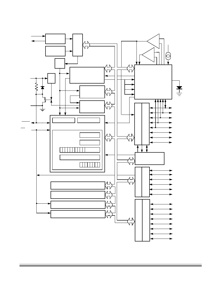
Figure 1-1. User Mode Block Diagram
˜
2
SIMPLE SERIAL
INTERFACE
(SIOP)
T
R
A
N
SF
ER
CO
NT
R
O
L
STK PTR
WATCHDOG &
ILLEGAL ADDR
DETECT
16-BIT TIMER
(1) INPUT CAPTURE
(1) OUTPUT COMPARE
EXTERNAL
OSCILLATOR
COND CODE REG
1 1 1
I N Z C
H
INDEX REG
CPU CONTROL
0 0 0
1
1
0
0
0
0
0
RESET
OSC1
OSC2
STATIC RAM (4T) -- 224 BYTES
ALU
68HC05 CPU
ACCUM
PROGRAM COUNTER
CPU REGISTERS
PA0*
PA1*
PA2*
PA3*
PA4*
POR
T
A
D
A
T
A
D
I
R.
RE
G.
PO
R
T
A
PB4/AN4/TCMP/CMP1*
PB3/AN3/TCAP
USER EPROM -- 6160 BYTES
* High sink current capability
* High source current capability
IRQ interrupt capability
PB2/AN2
PB1/AN1
PB0/AN0
15-STAGE
CORE TIMER
SYSTEM
INTERNAL
OSCILLATOR
INT
INT
V
SS
V
DD
+
≠
COMPARATOR
CONTROL &
MULTIPLEXER
TCMP
V
DD
CURRENT
SOURCE
+
≠
COMP2
COMP1
TCAP
INT
PB7/SCK
PB6/SDI
PB5/SDO
PA5*
LVR
PO
R
T
B
PO
R
T
B
D
A
T
A
DI
R. R
E
G
.
OCF
TOF
ICF
TEMPERATURE
DIODE
V
SS
PC3*
PC4*
PC5*
PC6*
PC7*
PC0*
PC1*
PC2*
PO
R
T
C
P
O
R
T
C D
A
T
A
D
I
R.
RE
G.
PORT C
ONLY ON
28-PIN
VERSIONS
V
SS
PERSONALITY EPROM -- 64 BITS
IRQ/V
PP
BOOT ROM -- 240 BYTES
Advance Information
MC68HC705JJ7 ∑ MC68HC705JP7 -- REV 4
28
General Description
MOTOROLA
General Description
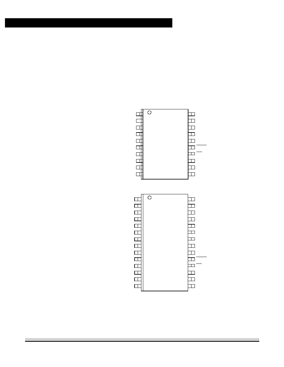
1.5 Functional Pin Description
Refer to
Figure 1-2
for the pinouts of the MC68HC705JJ7 and
MC68HC705JP7 in the user mode.
The following paragraphs give a description of the general function of
each pin.
Figure 1-2. User Mode Pinouts
* Denotes 10 mA sink /5 mA source capability
Denotes IRQ interrupt capability
PB0/AN0
28
V
DD
27
26
25
OSC2
24
PC3*
23
PC2*
22
PC1*
21
PB1/AN1
1
PB2/AN2
2
PB3/AN3/TCAP
3
*PB4/AN4/TCMP/CMP1
4
PB5/SDO
5
* PC4
6
*PC5
7
* PC6
8
PC0*
20
RESET
19
*PC7
9
PB6/SDI
10
V
SS
OSC1
IRQ/V
PP
18
PA0*
17
PB7/SCK
11
*PA5
12
PA1*
16
PA2*
15
* PA4
13
* PA3
14
PB0/AN0
V
DD
OSC2
PB1/AN1
PB2/AN2
PB3/AN3/TCAP
*PB4/AN4/TCMP/CMP1
PB5/SDO
RESET
PB6/SDI
V
SS
OSC1
IRQ/V
PP
PA0*
PB7/SCK
*PA5
PA1*
PA2*
* PA4
* PA3
MC68HC705JJ7
MC68HC705JP7
20
19
18
17
16
1
2
3
4
5
15
6
14
13
7
8
12
11
9
10

General Description
VDD and VSS Pins
MC68HC705JJ7 ∑ MC68HC705JP7 -- REV 4
Advance Information
MOTOROLA
General Description
29
1.6 V
DD
and V
SS
Pins
Power is supplied to the MCU through V
DD
and V
SS
. V
DD
is the positive
supply, and V
SS
is ground. The MCU operates from a single power
supply.
Very fast signal transitions occur on the MCU pins. The short rise and fall
times place very high short-duration current demands on the power
supply. To prevent noise problems, special care should be taken to
provide good power supply bypassing at the MCU by using bypass
capacitors with good high-frequency characteristics that are positioned
as close to the MCU as possible.
1.7 OSC1 and OSC2 Pins
The OSC1 and OSC2 pins are the connections for the external pin
oscillator (EPO). The OSC1 and OSC2 pins can accept these sets of
components:
∑
A crystal as shown in
Figure 1-3
(a)
∑
A ceramic resonator as shown in
Figure 1-3
(a)
∑
An external resistor as shown in
Figure 1-3
(b)
∑
An external clock signal as shown in
Figure 1-3
(c)
The selection of the crystal/ceramic resonator or RC oscillator
configuration is done by product part number selection as described in
Section 17. Ordering Information
.
The frequency, f
OSC
, of the EPO or external clock source is divided by
two to produce the internal operating frequency, f
OP
.

Advance Information
MC68HC705JJ7 ∑ MC68HC705JP7 -- REV 4
30
General Description
MOTOROLA
General Description
Figure 1-3. EPO Oscillator Connections
1.7.1 Crystal Oscillator
The circuit in
Figure 1-3
(a) shows a typical oscillator circuit for an
AT-cut, parallel resonant crystal. The crystal manufacturer's
recommendations should be followed, as the crystal parameters
determine the external component values required to provide maximum
stability and reliable startup. The load capacitance values used in the
oscillator circuit design should include all stray capacitances. The crystal
and components should be mounted as close as possible to the pins for
startup stabilization and to minimize output distortion. An internal startup
resistor of approximately 2 M
can be provided between OSC1 and
OSC2 for the crystal type oscillator by use of the OSCRES bit in the
MOR.
1.7.2 Ceramic Resonator Oscillator
In cost-sensitive applications, a ceramic resonator can be used in place
of the crystal. The circuit in
Figure 1-3
(a) can be used for a ceramic
resonator. The resonator manufacturer's recommendations should be
followed, as the resonator parameters determine the external
component values required for maximum stability and reliable starting.
The load capacitance values used in the oscillator circuit design should
include all stray capacitances. The ceramic resonator and components
should be mounted as close as possible to the pins for startup
stabilization and to minimize output distortion. An internal startup resistor
MCU
(a) Crystal or
Ceramic Resonator
Connections
OSC1
OSC2
2 M
R
UNCONNECTED
EXTERNAL CLOCK
(b) RC Oscillator
Connections
(c) External Clock
Source Connection
OSC1
OSC2
MCU
OSC1
OSC2
MCU

General Description
OSC1 and OSC2 Pins
MC68HC705JJ7 ∑ MC68HC705JP7 -- REV 4
Advance Information
MOTOROLA
General Description
31
of approximately 2 M
can be provided between OSC1 and OSC2 for
the ceramic resonator type oscillator by use of the OSCRES bit in the
MOR.
1.7.3 RC Oscillator
The lowest cost oscillator is the RC oscillator configuration where a
resistor is connected between the two oscillator pins as shown
in
Figure 1-3
(b).
The selection of the RC oscillator configuration is done by product part
number selection as described in
Section 17. Ordering Information
.
NOTE:
Do not use the internal startup resistor between OSC1 and OSC2 for the
RC-type oscillator.
1.7.4 External Clock
An external clock from another CMOS-compatible device can be
connected to the OSC1 input, with the OSC2 input not connected, as
shown in
Figure 1-3
(c). This oscillator can be selected via software.
This configuration is possible regardless of whether the crystal/ceramic
resonator or RC oscillator configuration is used.
NOTE:
Do not use the internal startup resistor between OSC1 and OSC2 for the
external clock.
1.7.5 Internal Low-Power Oscillator
An internal low-power oscillator (LPO) is provided which is the default
oscillator out of reset. When operating from this internal LPO, the other
oscillator can be powered down by software to further conserve power.
The selection of the LPO configuration is done by product part number
selection as described in
Section 17. Ordering Information
.

Advance Information
MC68HC705JJ7 ∑ MC68HC705JP7 -- REV 4
32
General Description
MOTOROLA
General Description
1.8 RESET Pin
The RESET pin can be used as an input to reset the MCU to a known
startup state by pulling it to the low state. It also functions as an output
to indicate that an internal COP watchdog, illegal address, or low-voltage
reset has occurred. The RESET pin contains a pullup device to allow the
pin to be left disconnected without an external pullup resistor. The
RESET pin also contains a steering diode that, when the power is
removed, will discharge to V
DD
any charge left on an external capacitor
connected between the RESET pin and V
SS
. The RESET pin also
contains an internal Schmitt trigger to improve its noise immunity as an
input.
1.9 IRQ/V
PP
Pin
The IRQ/V
PP
input pin drives the asynchronous IRQ interrupt function of
the CPU. The IRQ interrupt function uses the LEVEL bit in the MOR to
provide either negative edge-sensitive triggering or both negative
edge-sensitive and low level-sensitive triggering. If the LEVEL bit is set
to enable level-sensitive triggering, the IRQ/V
PP
pin requires an external
resistor to V
DD
for "wired-OR" operation. If the IRQ/V
PP
pin is not used,
it must be tied to the V
DD
supply. The IRQ/V
PP
pin contains an internal
Schmitt trigger as part of its input to improve noise immunity.
The voltage on this pin may affect operation if the voltage on the
IRQ/V
PP
pin is above V
DD
when the device is released from a reset
condition. The IRQ/V
PP
pin should only be taken above V
DD
to program
an EPROM memory location or personality EPROM bit. For more
information, refer to
15.14 PEPROM and EPROM Programming
Characteristics
.
NOTE:
Each of the PA0≠PA3 I/O pins may be connected as an OR function with
the IRQ interrupt function by the PIRQ bit in the MOR. This capability
allows keyboard scan applications where the transitions or levels on the
I/O pins will behave the same as the IRQ/V
PP
pin, except that active
transitions and levels are inverted. The edge or level sensitivity selected
by the LEVEL bit in the MOR for the IRQ/V
PP
pin also applies to the I/O

General Description
PA0≠PA5
MC68HC705JJ7 ∑ MC68HC705JP7 -- REV 4
Advance Information
MOTOROLA
General Description
33
pins that are ORed to create the IRQ signal. For more information, refer
to
4.6 External Interrupts
.
1.10 PA0≠PA5
These six I/O lines comprise port A, a general-purpose bidirectional I/O
port. This port also has four pins which have keyboard interrupt
capability. All six of these pins have high current source and sink
capability.
All of these pins have software programmable pulldowns which can be
disabled by the SWPDI bit in the MOR.
1.11 PB0≠PB7
These eight I/O lines comprise port B, a general-purpose bidirectional
I/O port. This port is also shared with the 16-bit programmable timer
input capture and output compare functions, with the two voltage
comparators in the analog subsystem, and with the simple serial
interface (SIOP).
The outputs of voltage comparator 1 can directly drive the PB4 pin; and
the PB4 pin has high current source and sink capability.
All of these pins have software programmable pulldowns which can be
disabled by the SWPDI bit in the MOR.
1.12 PC0≠PC7 (MC68HC705JP7)
These eight I/O lines comprise port C, a general-purpose bidirectional
I/O port. This port is only available on the 28-pin MC68HC705JP7. All
eight of these pins have high current source and sink capability.
All of these pins have software programmable pulldowns which can be
disabled by the SWPDI bit in the MOR.

Advance Information
MC68HC705JJ7 ∑ MC68HC705JP7 -- REV 4
34
General Description
MOTOROLA
General Description

MC68HC705JJ7 ∑ MC68HC705JP7 -- REV 4
Advance Information
MOTOROLA
Memory
35
Advance Information -- MC68HC705JJ7/MC68HC705JP7
Section 2. Memory
2.1 Contents
2.2
Introduction . . . . . . . . . . . . . . . . . . . . . . . . . . . . . . . . . . . . . . . . 35
2.3
Memory Map. . . . . . . . . . . . . . . . . . . . . . . . . . . . . . . . . . . . . . . 36
2.4
Input/Output Registers . . . . . . . . . . . . . . . . . . . . . . . . . . . . . . . 36
2.5
User and Interrupt Vector Mapping. . . . . . . . . . . . . . . . . . . . . . 42
2.6
Random-Access Memory (RAM) . . . . . . . . . . . . . . . . . . . . . . . 42
2.7
Erasable Programmable Read-Only Memory (EPROM) . . . . . 43
2.8
COP Register . . . . . . . . . . . . . . . . . . . . . . . . . . . . . . . . . . . . . . 43
2.2 Introduction
This section describes the organization of the memory on the
MC68HC705JJ7/MC68HC705JP7.

Advance Information
MC68HC705JJ7 ∑ MC68HC705JP7 -- REV 4
36
Memory
MOTOROLA
Memory
2.3 Memory Map
The central processor unit (CPU) can address 8 kilobytes of memory
space as shown in
Figure 2-1
. The memory map includes:
∑
The erasable programmable read-only memory (EPROM) portion
of memory holds the program instructions, fixed data,
user-defined vectors, and interrupt service routines.
∑
The random-access memory (RAM) portion of memory holds
variable data.
∑
Input/output (I/O) registers are memory mapped so that the CPU
can access their locations in the same way that it accesses all
other memory locations.
2.4 Input/Output Registers
Figure 2-2
and
Figure 2-3
summarize:
∑
The first 32 addresses of the memory space, $0000≠$001F,
containing the I/O registers section
∑
One I/O register located outside the 32-byte I/O section, which is
the computer operating properly register (COPR) mapped at
$1FF0
$1EFF
Figure 2-1. Memory Map

Memory
Input/Output Registers
MC68HC705JJ7 ∑ MC68HC705JP7 -- REV 4
Advance Information
MOTOROLA
Memory
37
Address
Register Name
$0000
Port A Data Register
$0001
Port B Data Register
$0002
Port C Data Register *
$0003
Analog MUX Register
$0004
Port A Data Direction Register
$0005
Port B Data Direction Register
$0006
Port C Data Direction Register *
$0007
Unused
$0008
Core Timer Status & Control Register
$0009
Core Timer Counter
$000A
Serial Control Register
$000B
Serial Status Register
$000C
Serial Data Register
$000D
IRQ Status & Control Register
$000E
Personality EPROM Bit Select Register
$000F
Personality EPROM Status & Control Register
$0010
Port A and Port C Pulldown Register *
$0011
Port B Pulldown Register
$0012
Timer Control Register
$0013
Timer Status Register
$0014
Input Capture Register (MSB)
$0015
Input Capture Register (LSB)
$0016
Output Compare Register (MSB)
$0017
Output Compare Register (LSB)
$0018
Timer Counter Register (MSB)
$0019
Timer Counter Register (LSB)
$001A
Alternate Counter Register (MSB)
$001B
Alternate Counter Register (LSB)
$001C
EPROM Programming Register
$001D
Analog Control Register
$001E
Analog Status Register
$001F
Reserved
* Features related to port C are only available on the 28-pin
MC68HC705JP7 devices.
Figure 2-2. I/O Registers
Advance Information
MC68HC705JJ7 ∑ MC68HC705JP7 -- REV 4
38
Memory
MOTOROLA
Memory
Addr.
Register
Bit 7
6
5
4
3
2
1
Bit 0
$0000
Port A Data Register
(PORTA)
See page 85.
Read:
0
0
PA5
PA4
PA3
PA2
PA1
PA0
Write:
Reset:
Unaffected by reset
$0001
Port B Data Register
(PORTB)
See page 90.
Read:
PB7
PB6
PB5
PB4
PB3
PB2
PB1
PB0
Write:
Reset:
Unaffected by reset
$0002
Port C
(1)
Data Register
(PORTC)
See page 102.
Read:
PC7
PC6
PC5
PC4
PC3
PC2
PC1
PC0
Write:
Reset:
Unaffected by reset
$0003
Analog Multiplex Register
(AMUX)
See page 110.
Read:
HOLD
DHOLD
INV
VREF
MUX4
MUX3
MUX2
MUX1
Write:
Reset:
1
0
0
0
0
0
0
0
$0004
Data Direction Register A
(DDRA)
See page 86.
Read:
0
0
DDRA5
DDRA4
DDRA3
DDRA2
DDRA1
DDRA0
Write:
Reset:
0
0
0
0
0
0
0
0
$0005
Data Direction Register B
(DDRB)
See page 91.
Read:
DDRB7
DDRB6
DDRB5
DDRB4
DDRB3
DDRB2
DDRB1
DDRB0
Write:
Reset:
0
0
0
0
0
0
0
0
$0006
Data Direction Register C
(DDRC)
See page 103.
Read:
DDRC7
DDRC6
DDRC5
DDRC4
DDRC3
DDRC2
DDRC1
DDRC0
Write:
Reset:
0
0
0
0
0
0
0
0
$0007
Unimplemented
$0008
Core Timer Status and Control
Register (CTSCR)
See page 153.
Read:
CTOF
RTIF
CTOFE
RTIE
0
0
RT1
RT0
Write:
CTOFR
RTIFR
Reset:
0
0
0
0
0
0
1
1
$0009
Core Timer Counter Register
(CTCR)
See page 155.
Read:
Bit 7
6
5
4
3
2
1
Bit 0
Write:
Reset:
0
0
0
0
0
0
0
0
= Unimplemented
R
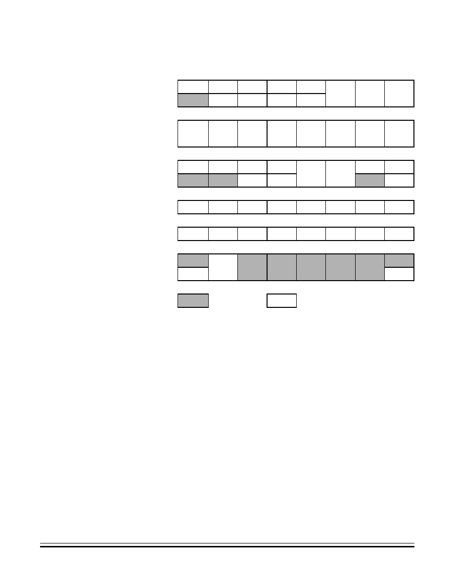
= Reserved
U = Unaffected
1.
Features related to port C are only available on the 28-pin MC68HC705JP7 devices.
Figure 2-3. Register Summary (Sheet 1 of 4)
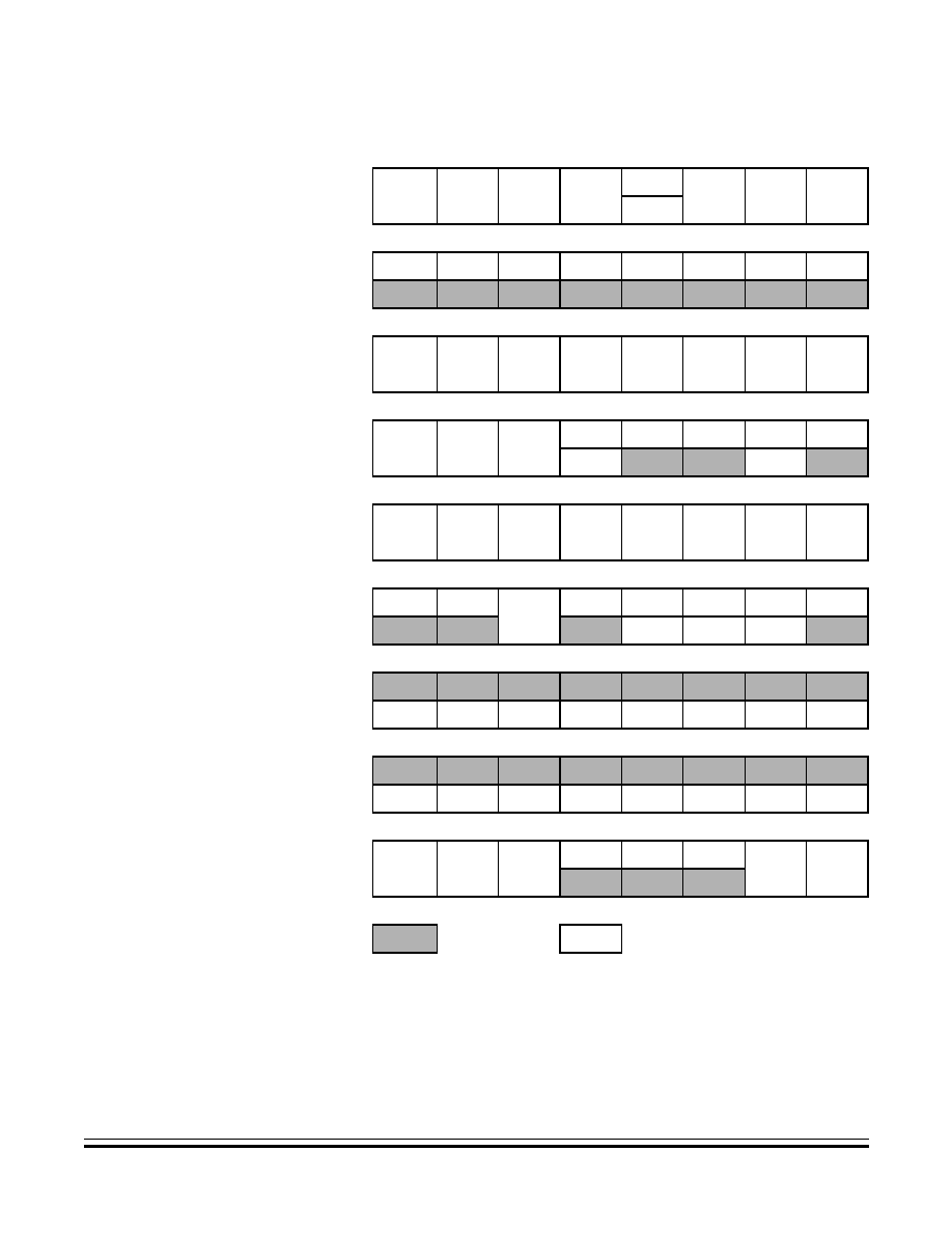
Memory
Input/Output Registers
MC68HC705JJ7 ∑ MC68HC705JP7 -- REV 4
Advance Information
MOTOROLA
Memory
39
$000A
SIOP Control Register
(SCR)
See page 145.
Read:
SPIE
SPE
LSBF
MSTR
0
CPHA
SPR1
SPR0
Write:
SPIR
Reset:
0
0
0
0
0
0
0
0
$000B
SIOP Status Register
(SSR)
See page 148.
Read:
SPIF
DCOL
0
0
0
0
0
0
Write:
Reset:
0
0
0
0
0
0
0
0
$000C
SIOP Data Register
(SDR)
See page 149.
Read:
Bit 7
6
5
4
3
2
1
Bit 0
Write:
Reset:
$000D
IRQ Status and Control Register
(ISCR)
See page 58.
Read:
IRQE
OM2
OM1
0
IRQF
0
0
0
Write:
R
IRQR
Reset:
1
1
0
0
0
0
U
0
$000E
PEPROM Bit Select Register
(PEBSR)
See page 177.
Read:
PEB7
PEB6
PEB5
PEB4
PEB3
PEB2
PEB1
PEB0
Write:
Reset:
0
0
0
0
0
0
0
0
$000F
PEPROM Status and Control
Register (PESCR)
See page 178.
Read: PEDATA
0
PEPGM
0
0
0
0
PEPRZF
Write:
R
R
R
Reset:
U
0
0
0
0
0
0
1
$0010
Pulldown Register Port A and
Port C
(1)
(PDRA)
See page 87.
Read:
Write:
PDICH
PDICL
PDIA5
PDIA4
PDIA3
PDIA2
PDIA1
PDIA0
Reset:
0
0
0
0
0
0
0
0
$0011
Pulldown Register B
(PDRB)
See page 92.
Read:
Write:
PDIB7
PDIB6
PDIB5
PDIB4
PDIB3
PDIB2
PDIB1
PDIB0
Reset:
0
0
0
0
0
0
0
0
$0012
Timer Control Register
(TCR)
See page 170.
Read:
ICIE
OCIE
TOIE
0
0
0
IEDG
OLVL
Write:
Reset:
0
0
0
0
0
0
U
0
Addr.
Register
Bit 7
6
5
4
3
2
1
Bit 0
= Unimplemented
R
= Reserved
U = Unaffected
1.
Features related to port C are only available on the 28-pin MC68HC705JP7 devices.
Figure 2-3. Register Summary (Sheet 2 of 4)

Advance Information
MC68HC705JJ7 ∑ MC68HC705JP7 -- REV 4
40
Memory
MOTOROLA
Memory
$0013
Timer Status Register
(TSR)
See page 172.
Read:
ICF
OCF
TOF
0
0
0
0
0
Write:
Reset:
U
U
U
0
0
0
0
0
$0014
Input Capture Register High
(ICRH)
See page 166.
Read:
Bit 15
14
13
12
11
10
9
Bit 8
Write:
Reset:
Unaffected by reset
$0015
Input Capture Register Low
(ICRL)
See page 166.
Read:
Bit 7
6
5
4
3
2
1
Bit 0
Write:
Reset:
Unaffected by reset
$0016
Output Compare Register High
(OCRH)
See page 168.
Read:
Bit 15
14
13
12
11
10
9
Bit 8
Write:
Reset:
Unaffected by reset
$0017
Output Compare Register Low
(OCRL)
See page 168.
Read:
Bit 7
6
5
4
3
2
1
Bit 0
Write:
Reset:
Unaffected by reset
$0018
Programmable Timer Register
High (TMRH)
See page 163.
Read:
Bit 15
14
13
12
11
10
9
Bit 8
Write:
Reset:
1
1
1
1
1
1
1
1
$0019
Programmable Timer Register
Low (TMRL)
See page 163.
Read:
Bit 7
6
5
4
3
2
1
Bit 0
Write:
Reset:
1
1
1
1
1
1
0
0
$001A
Alternate Counter Register High
(ACRH)
See page 165.
Read:
Bit 15
14
13
12
11
10
9
Bit 8
Write:
Reset:
1
1
1
1
1
1
1
1
$001B
Alternate Counter Register Low
(ACRL)
See page 165.
Read:
Bit 15
14
13
12
11
10
9
Bit 8
Write:
Reset:
1
1
1
1
1
1
0
0
Addr.
Register
Bit 7
6
5
4
3
2
1
Bit 0
= Unimplemented
R
= Reserved
U = Unaffected
1.
Features related to port C are only available on the 28-pin MC68HC705JP7 devices.
Figure 2-3. Register Summary (Sheet 3 of 4)
Memory
Input/Output Registers
MC68HC705JJ7 ∑ MC68HC705JP7 -- REV 4
Advance Information
MOTOROLA
Memory
41
$001C
EPROM Programming Register
(EPROG)
See page 184.
Read:
0
0
0
0
0
ELAT
MPGM
EPGM
Write:
R
R
R
R
Reset:
0
0
0
0
0
0
0
0
$001D
Analog Counter Register
(ACR)
See page 115.
Read:
CHG
ATD2
ATD1
ICEN
CPIE
CP2EN
CP1EN
ISEN
Write:
Reset:
0
0
0
0
0
0
0
0
$001E
Analog Status Register
(ASR)
See page 115.
Read:
CPF2
CPF1
0
0
COE1
VOFF
CMP2
CMP1
Write:
CPFR2
CPFR1
R
Reset:
0
0
0
0
0
0
0
0
$001F
Reserved
R
R
R
R
R
R
R
R
$1FEF
Reserved
R
R
R
R
R
R
R
R
$1FF0
COP and Security Register
(COPR)
See pages 43
,
137
,
156
, and
188
.
Read:
OPT
Write: EPMSEC
COPC
Reset:
Unaffected by reset
Addr.
Register
Bit 7
6
5
4
3
2
1
Bit 0
= Unimplemented
R
= Reserved
U = Unaffected
1.
Features related to port C are only available on the 28-pin MC68HC705JP7 devices.
Figure 2-3. Register Summary (Sheet 4 of 4)

Advance Information
MC68HC705JJ7 ∑ MC68HC705JP7 -- REV 4
42
Memory
MOTOROLA
Memory
2.5 User and Interrupt Vector Mapping
The interrupt vectors are contained in the upper memory addresses
above $1FF0 as shown in
Figure 2-4
.
2.6 Random-Access Memory (RAM)
The 224 addresses from $0020 to $00FF serve as both the user RAM
and the stack RAM. The central processor unit (CPU) uses five RAM
bytes to save all CPU register contents before processing an interrupt.
During a subroutine call, the CPU uses two bytes to store the return
address. The stack pointer decrements during pushes and increments
during pulls.
NOTE:
Be careful when using nested subroutines or multiple interrupt levels.
The CPU may overwrite data in the RAM during a subroutine or during
the interrupt stacking operation.
Address
Register Name
$1FF0
COP Register and EPROM Security
$1FF1
Mask Option Register
$1FF2
Analog Interrupt Vector (MSB)
$1FF3
Analog Interrupt Vector (LSB)
$1FF4
Serial Interrupt Vector (MSB)
$1FF5
Serial Interrupt Vector ((LSB)
$1FF6
Timer Interrupt Vector (MSB)
$1FF7
Timer Interrupt Vector (LSB)
$1FF8
Core Timer Interrupt Vector (MSB)
$1FF9
Core Timer Interrupt Vector (LSB)
$1FFA
External IRQ Vector (MSB)
$1FFB
External IRQ Vector (LSB)
$1FFC
SWI Vector (MSB)
$1FFD
SWI Vector (LSB)
$1FFE
Reset Vector (MSB)
$1FFF
Reset Vector (LSB)
Figure 2-4. Vector Mapping

Memory
Erasable Programmable Read-Only Memory (EPROM)
MC68HC705JJ7 ∑ MC68HC705JP7 -- REV 4
Advance Information
MOTOROLA
Memory
43
2.7 Erasable Programmable Read-Only Memory (EPROM)
The EPROM is located in three areas of the memory map:
∑
Addresses $0700≠$1EFF contain 6144 bytes of user EPROM.
∑
Addresses $1FF0≠$1FF1 contain 2 bytes of EPROM reserved for
user vectors and COP and security register (COPR), and the mask
option register. Only bit 7 of $1FF0 is a programmable bit.
∑
Addresses $1FF2≠$1FFF contain 14 bytes of interrupt vectors.
2.8 COP Register
As shown in
Figure 2-5
, a register location is provided at $1FF0 to set
the EPROM security
(1)
, select the optional features, and reset the COP
watchdog timer. The OPT bit controls the function of the PB4 port pin
and the availability to add an offset to any measured analog voltages.
See
8.5 Analog Status Register
for more information
1. No security feature is absolutely secure. However, Motorola's strategy is to make reading or
copying the EPROM/OTPROM difficult for unauthorized users.
Address: $1FF0
$1FF0
Bit 7
6
5
4
3
2
1
Bit 0
Read:
OPT
Write: EPMSEC
COPC
Reset:
Unaffected by reset
= Unimplemented
Figure 2-5. COP and Security Register (COPR)

Advance Information
MC68HC705JJ7 ∑ MC68HC705JP7 -- REV 4
44
Memory
MOTOROLA
Memory

MC68HC705JJ7 ∑ MC68HC705JP7 -- REV 4
Advance Information
MOTOROLA
Central Processor Unit (CPU)
45
Advance Information -- MC68HC705JJ7/MC68HC705JP7
Section 3. Central Processor Unit (CPU)
3.1 Contents
3.2
Introduction . . . . . . . . . . . . . . . . . . . . . . . . . . . . . . . . . . . . . . . . 45
3.3
Accumulator . . . . . . . . . . . . . . . . . . . . . . . . . . . . . . . . . . . . . . . 46
3.4
Index Register. . . . . . . . . . . . . . . . . . . . . . . . . . . . . . . . . . . . . . 47
3.5
Stack Pointer . . . . . . . . . . . . . . . . . . . . . . . . . . . . . . . . . . . . . . 47
3.6
Program Counter . . . . . . . . . . . . . . . . . . . . . . . . . . . . . . . . . . . 48
3.7
Condition Code Register. . . . . . . . . . . . . . . . . . . . . . . . . . . . . .48
3.8
Arithmetic/Logic Unit (ALU) . . . . . . . . . . . . . . . . . . . . . . . . . . .50
3.2 Introduction
This section describes the central processor unit (CPU) registers.
Figure 3-1
shows the five CPU registers. CPU registers are not part of
the memory map.
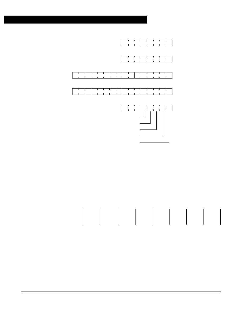
Advance Information
MC68HC705JJ7 ∑ MC68HC705JP7 -- REV 4
46
Central Processor Unit (CPU)
MOTOROLA
Central Processor Unit (CPU)
Figure 3-1. M68HC05 Programming Model
3.3 Accumulator
The accumulator is a general-purpose 8-bit register as shown in
Figure 3-2
. The CPU uses the accumulator to hold operands and results
of arithmetic and non-arithmetic operations.
ACCUMULATOR (A)
A
INDEX REGISTER (X)
X
SP
1
1
0
0
0
0
0
0
0
0
PCL
PCH
1
1
1
Z
C
I
N
1
H
1
1
0
4
7
5
CONDITION CODE REGISTER (CCR)
PROGRAM COUNTER (PC)
STACK POINTER (SP)
0
7
8
15
15
5
7
7
0
0
0
HALF-CARRY FLAG
INTERRUPT MASK
NEGATIVE FLAG
ZERO FLAG
CARRY/BORROW FLAG
10
6
Bit 7
6
5
4
3
2
1
Bit 0
Read:
Write:
Reset:
Unaffected by reset
Figure 3-2. Accumulator (A)
Central Processor Unit (CPU)
Index Register
MC68HC705JJ7 ∑ MC68HC705JP7 -- REV 4
Advance Information
MOTOROLA
Central Processor Unit (CPU)
47
3.4 Index Register
The index register is a general-purpose 8-bit register as shown in
Figure 3-3
. In the indexed addressing modes, the CPU uses the byte in
the index register to determine the conditional address of the operand.
The 8-bit index register can also serve as a temporary data storage
location.
3.5 Stack Pointer
The stack pointer is a 16-bit register that contains the address of the next
location on the stack as shown in
Figure 3-4
. During a reset or after the
reset stack pointer (RSP) instruction, the stack pointer initializes to
$00FF. The address in the stack pointer decrements as data is pushed
onto the stack and increments as data is pulled from the stack.
The 10 most significant bits of the stack pointer are permanently fixed at
0000000011, so the stack pointer produces addresses from $00C0 to
$00FF. If subroutines and interrupts use more than 64 stack locations,
the stack pointer wraps around to address $00FF and begins writing
over the previously stored data. A subroutine uses two stack locations;
an interrupt uses five locations.
Bit 7
6
5
4
3
2
1
Bit 0
Read:
Write:
Reset:
Unaffected by reset
Figure 3-3. Index Register (X)
Bit
15
14
13
12
11
10
9
8
7
6
5
4
3
2
1
Bit
0
Read:
0
0
0
0
0
0
0
0
1
1
Write:
Reset:
0
0
0
0
0
0
0
0
1
1
1
1
1
1
1
1
Figure 3-4. Stack Pointer (SP)
Advance Information
MC68HC705JJ7 ∑ MC68HC705JP7 -- REV 4
48
Central Processor Unit (CPU)
MOTOROLA
Central Processor Unit (CPU)
3.6 Program Counter
The program counter is a 16-bit register that contains the address of the
next instruction or operand to be fetched as shown in
Figure 3-5
. The
three most significant bits of the program counter are ignored internally
and appear as 111 during stacking and subroutine calls.
Normally, the address in the program counter automatically increments
to the next sequential memory location every time an instruction or
operand is fetched. Jump, branch, and interrupt operations load the
program counter with an address other than that of the next sequential
location.
3.7 Condition Code Register
The condition code register is an 8-bit register whose three most
significant bits are permanently fixed at 111 as shown in
Figure 3-6
. The
condition code register contains the interrupt mask and four flags that
indicate the results of the instruction just executed. The following
paragraphs describe the functions of the condition code register.
Bit
15
14
13
12
11
10
9
8
7
6
5
4
3
2
1
Bit
0
Read:
1
1
1
Write:
Reset:
0
0
0
Loaded with vector from $1FFE and $1FFF
Figure 3-5. Program Counter (PC)
Bit 7
6
5
4
3
2
1
Bit 0
Read:
1
1
1
H
I
N
C
Z
Write:
Reset:
1
1
1
U
1
U
U
U
U = Unaffected
Figure 3-6. Condition Code Register (CCR)

Central Processor Unit (CPU)
Condition Code Register
MC68HC705JJ7 ∑ MC68HC705JP7 -- REV 4
Advance Information
MOTOROLA
Central Processor Unit (CPU)
49
Half-Carry Flag (H)
The CPU sets the half-carry flag when a carry occurs between bits 3
and 4 of the accumulator during an ADD or ADC operation. The
half-carry flag is required for binary coded decimal (BCD) arithmetic
operations. Reset has no effect on the half-carry flag.
Interrupt Mask (I)
Setting the interrupt mask disables interrupts. If an interrupt request
occurs while the interrupt mask is a logic 0, the CPU saves the CPU
registers on the stack, sets the interrupt mask, and then fetches the
interrupt vector. If an interrupt request occurs while the interrupt mask
is set, the interrupt request is latched. The CPU processes the latched
interrupt as soon as the interrupt mask is cleared again.
A return-from-interrupt (RTI) instruction pulls the CPU registers from
the stack, restoring the interrupt mask to its cleared state. After a
reset, the interrupt mask is set and can be cleared only by a CLI
instruction.
Negative Flag (N)
The CPU sets the negative flag when an arithmetic operation, logical
operation, or data manipulation produces a negative result. Reset has
no affect on the negative flag.
Zero Flag (Z)
The CPU sets the zero flag when an arithmetic operation, logical
operation, or data manipulation produces a result of $00. Reset has
no affect on the zero flag.
Carry/Borrow Flag (C)
The CPU sets the carry/borrow flag when an addition operation
produces a carry out of bit 7 of the accumulator or when a subtraction
operation requires a borrow. Some logical operations and data
manipulation instructions also clear or set the carry/borrow flag. Reset
has no effect on the carry/borrow flag.

Advance Information
MC68HC705JJ7 ∑ MC68HC705JP7 -- REV 4
50
Central Processor Unit (CPU)
MOTOROLA
Central Processor Unit (CPU)
3.8 Arithmetic/Logic Unit (ALU)
The ALU performs the arithmetic and logical operations defined by the
instruction set. The binary arithmetic circuits decode instructions and set
up the ALU for the selected operation. Most binary arithmetic is based
on the addition algorithm, carrying out subtraction as negative addition.
Multiplication is not performed as a discrete operation but as a chain of
addition and shift operations within the ALU. The multiply instruction
(MUL) requires 11 internal clock cycles to complete this chain of
operations.

MC68HC705JJ7 ∑ MC68HC705JP7 -- REV 4
Advance Information
MOTOROLA
Interrupts
51
Advance Information -- MC68HC705JJ7/MC68HC705JP7
Section 4. Interrupts
4.1 Contents
4.2
Introduction . . . . . . . . . . . . . . . . . . . . . . . . . . . . . . . . . . . . . . . . 51
4.3
Interrupt Vectors . . . . . . . . . . . . . . . . . . . . . . . . . . . . . . . . . . . . 52
4.4
Interrupt Processing . . . . . . . . . . . . . . . . . . . . . . . . . . . . . . . . . 53
4.5
Software Interrupt . . . . . . . . . . . . . . . . . . . . . . . . . . . . . . . . . . . 55
4.6
External Interrupts . . . . . . . . . . . . . . . . . . . . . . . . . . . . . . . . . .55
4.6.1
IRQ/V
PP
Pin . . . . . . . . . . . . . . . . . . . . . . . . . . . . . . . . . . . . . 55
4.6.2
PA0≠PA3 Pins . . . . . . . . . . . . . . . . . . . . . . . . . . . . . . . . . . . 57
4.6.3
IRQ Status and Control Register (ISCR) . . . . . . . . . . . . . . . 58
4.7
Core Timer Interrupts . . . . . . . . . . . . . . . . . . . . . . . . . . . . . . . . 60
4.7.1
Core Timer Overflow Interrupt . . . . . . . . . . . . . . . . . . . . . . . 60
4.7.2
Real-Time Interrupt . . . . . . . . . . . . . . . . . . . . . . . . . . . . . . . 60
4.8
Programmable Timer Interrupts . . . . . . . . . . . . . . . . . . . . . . . . 61
4.8.1
Input Capture Interrupt . . . . . . . . . . . . . . . . . . . . . . . . . . . . . 61
4.8.2
Output Compare Interrupt . . . . . . . . . . . . . . . . . . . . . . . . . . 61
4.8.3
Timer Overflow Interrupt. . . . . . . . . . . . . . . . . . . . . . . . . . . . 61
4.9
Serial Interrupts . . . . . . . . . . . . . . . . . . . . . . . . . . . . . . . . . . . . 62
4.10
Analog Interrupts . . . . . . . . . . . . . . . . . . . . . . . . . . . . . . . . . . . 62
4.10.1
Comparator Input Match Interrupt . . . . . . . . . . . . . . . . . . . .63
4.10.2
Input Capture Interrupt . . . . . . . . . . . . . . . . . . . . . . . . . . . . . 63
4.2 Introduction
An interrupt temporarily stops normal program execution to process a
particular event. An interrupt does not stop the execution of the
instruction in progress, but takes effect when the current instruction
completes its execution. Interrupt processing automatically saves the

Advance Information
MC68HC705JJ7 ∑ MC68HC705JP7 -- REV 4
52
Interrupts
MOTOROLA
Interrupts
central processor unit (CPU) registers on the stack and loads the
program counter with a user-defined vector address.
4.3 Interrupt Vectors
Table 4-1
summarizes the reset and interrupt sources and vector
assignments.
NOTE:
If more than one interrupt request is pending, the CPU fetches the vector
of the higher priority interrupt first. A higher priority interrupt does not
actually interrupt a lower priority interrupt service routine unless the
lower priority interrupt service routine clears the I bit.
Table 4-1. Reset/Interrupt Vector Addresses
Function
Source
MOR
Control
Bit
Global
Hardware
Mask
Local
Software
Mask
Priority
(1 = Highest)
Vector
Address
Reset
Power-on logic
RESET pin
Low-voltage reset
Illegal address reset
--
--
--
1
$1FFE≠$1FFF
COP watchdog
COPEN
(1)
Software
interrupt (SWI)
User code
--
--
--
Same priority
as instruction
$1FFC≠$1FFD
External
interrupt (IRQ)
IRQ/V
PP
pin
--
I bit
IRQE bit
2
$1FFA≠$1FFB
PA3 pin
PA2 pin
PA1 pin
PA0 pin
PIRQ
(2)
Core timer
interrupts
TOF bit
RTIF bit
--
I bit
TOFE bit
RTIE bit
3
$1FF8≠$1FF9
Programmable
timer interrupts
ICF bit
OCF bit
TOF bit
--
I bit
ICIE bit
OCIE bit
TOIE bit
4
$1FF6≠$1FF7
Serial interrupt
SPIF bit
--
I bit
SPIE bit
5
$1FF4≠$1FF5
Analog interrupt
CPF1 bit
CPF2 bit
--
I bit
CPIE bit
6
$1FF2≠$1FF3
1. COPEN enables the COP watchdog timer.
2. PIRQ enables port A external interrupts on PA0≠PA3.
Interrupts
Interrupt Processing
MC68HC705JJ7 ∑ MC68HC705JP7 -- REV 4
Advance Information
MOTOROLA
Interrupts
53
4.4 Interrupt Processing
To begin servicing an interrupt, the CPU does these actions:
∑
Stores the CPU registers on the stack in the order shown in
Figure 4-1
∑
Sets the I bit in the condition code register to prevent further
interrupts
∑
Loads the program counter with the contents of the appropriate
interrupt vector locations as shown in
Table 4-1
The return-from-interrupt (RTI) instruction causes the CPU to recover its
register contents from the stack as shown in
Figure 4-1
. The sequence
of events caused by an interrupt is shown in the flowchart in
Figure 4-2
.
$0020
Bottom of RAM
$0021
$00BE
$00BF
$00C0
Bottom of Stack
$00C1
$00C2
Unstacking
Order
n
Condition Code Register
5
1
n+1
Accumulator
4
2
n+2
Index Register
3
3
n+3
Program Counter (High Byte)
2
4
n+4
Program Counter (Low Byte)
1
5
Stacking
Order
$00FD
$00FE
$00FF
Top of Stack (RAM)
Figure 4-1. Interrupt Stacking Order

Advance Information
MC68HC705JJ7 ∑ MC68HC705JP7 -- REV 4
54
Interrupts
MOTOROLA
Interrupts
Figure 4-2. Interrupt Flowchart
NO
EXTERNAL
INTERRUPT?
I BIT SET?
FROM
RESET
YES
YES
CLEAR IRQ LATCH
NO
EXECUTE INSTRUCTION
UNSTACK CCR, A, X, PCH, PCL
FETCH NEXT
INSTRUCTION
STACK PCL, PCH, X, A, CCR
SET I BIT
LOAD PC WITH INTERRUPT VECTOR
CORE TIMER
INTERRUPT?
YES
NO
TIMER
INTERRUPT?
YES
NO
SERIAL
INTERRUPT?
YES
NO
ANALOG
INTERRUPT?
YES
NO
SWI
INSTRUCTION?
YES
NO
RTI
INSTRUCTION?
YES
NO

Interrupts
Software Interrupt
MC68HC705JJ7 ∑ MC68HC705JP7 -- REV 4
Advance Information
MOTOROLA
Interrupts
55
4.5 Software Interrupt
The software interrupt (SWI) instruction causes a non-maskable
interrupt.
4.6 External Interrupts
These sources can generate external interrupts:
∑
IRQ/V
PP
pin
∑
PA3≠PA0 pins
Setting the I bit in the condition code register or clearing the IRQE bit in
the interrupt status and control register disables these external
interrupts.
4.6.1 IRQ/V
PP
Pin
An interrupt signal on the IRQ/V
PP
pin latches an external interrupt
request. To help clean up slow edges, the input from the IRQ/V
PP
pin is
processed by a Schmitt trigger gate. When the CPU completes its
current instruction, it tests the IRQ latch. If the IRQ latch is set, the CPU
then tests the I bit in the condition code register and the IRQE bit in the
IRQ status and control register (ISCR). If the I bit is clear and the IRQE
bit is set, then the CPU begins the interrupt sequence. The CPU clears
the IRQ latch while it fetches the interrupt vector, so that another external
interrupt request can be latched during the interrupt service routine. As
soon as the I bit is cleared during the return from interrupt, the CPU can
recognize the new interrupt request.
Figure 4-3
shows the logic for
external interrupts.
NOTE:
If the IRQ/V
PP
pin is not in use, it should be connected to the V
DD
pin.
The IRQ/V
PP
pin can be negative edge-triggered only or negative edge-
and low level-triggered. External interrupt sensitivity is programmed with
the LEVEL bit in the mask option register (MOR).
Advance Information
MC68HC705JJ7 ∑ MC68HC705JP7 -- REV 4
56
Interrupts
MOTOROLA
Interrupts
Figure 4-3. External Interrupt Logic
With the edge- and level-sensitive trigger MOR option, a falling edge or
a low level on the IRQ/V
PP
pin latches an external interrupt request. The
edge- and level-sensitive trigger MOR option allows connection to the
IRQ/V
PP
pin of multiple wired-OR interrupt sources. As long as any
source is holding the IRQ low, an external interrupt request is present,
and the CPU continues to execute the interrupt service routine.
With the edge-sensitive-only trigger option, a falling edge on the
IRQ/V
PP
pin latches an external interrupt request. A subsequent
interrupt request can be latched only after the voltage level on the
IRQ/V
PP
pin returns to a logic 1 and then falls again to logic 0.
PA3
PA2
PA1
PA0
IRQ
LATCH
V
DD
RST
IRQ VECTOR FETCH
IRQ STATUS/CONTROL REGISTER ($000D)
EXTERNAL
INTERRUPT
REQUEST
IR
QE
IR
QF
IR
QR
INTERNAL DATA BUS
TO BIH & BIL
INSTRUCTION
PROCESSING
R
PI
R
Q
LE
VE
L
V
PP
TO
USER EPROM
AND PEPROM
MASK OPTION REGISTER ($1FF1)
IRQ/V
PP

Interrupts
External Interrupts
MC68HC705JJ7 ∑ MC68HC705JP7 -- REV 4
Advance Information
MOTOROLA
Interrupts
57
NOTE:
The response of the IRQ/V
PP
pin can be affected if the external interrupt
capability of the PA0 through PA3 pins is enabled. If the port A pins are
enabled as external interrupts, then any high level on a PA0≠PA3 pin will
cause the IRQ changes and state to be ignored until all of the PA0≠PA3
pins have returned to a low level.
4.6.2 PA0≠PA3 Pins
Programming the PIRQ bit in the MOR to a logic 1 enables the PA0≠PA3
pins (PA0:3) to serve as additional external interrupt sources. A rising
edge on a PA0:3 pin latches an external interrupt request. After
completing the current instruction, the CPU tests the IRQ latch. If the
IRQ latch is set, the CPU then tests the I bit in the condition code register
and the IRQE bit in the ISCR. If the I bit is clear and the IRQE bit is set,
the CPU then begins the interrupt sequence. The CPU clears the IRQ
latch while it fetches the interrupt vector, so that another external
interrupt request can be latched during the interrupt service routine. As
soon as the I bit is cleared during the return from interrupt, the CPU can
recognize the new interrupt request.
The PA0:3 pins can be edge-triggered or edge- and level-triggered.
External interrupt triggering sensitivity is selected by the LEVEL bit in the
MOR.
With the edge- and level-sensitive trigger MOR option, a rising edge or
a high level on a PA0:3 pin latches an external interrupt request. The
edge- and level-sensitive trigger MOR option allows connection to a
PA0:3 pin of multiple wired-OR interrupt sources. As long as any source
is holding the pin high, an external interrupt request is present, and the
CPU continues to execute the interrupt service routine.
With the edge-sensitive only trigger MOR option, a rising edge on a
PA0:3 pin latches an external interrupt request. A subsequent external
interrupt request can be latched only after the voltage level of the
previous interrupt signal returns to a logic 0 and then rises again to a
logic 1.
NOTE:
If the port A pins are enabled as external interrupts, then a high level on
any PA0:3 pin will drive the state of the IRQ function such that the
Advance Information
MC68HC705JJ7 ∑ MC68HC705JP7 -- REV 4
58
Interrupts
MOTOROLA
Interrupts
IRQ/V
PP
pin and other PA0:3 pins are to be ignored until ALL of the
PA0:3 pins have returned to a low level. Similarly, if the IRQ/V
PP
pin is
at a low level, the PA0:3 pins will be ignored until the IRQ/V
PP
pin returns
to a high state.
4.6.3 IRQ Status and Control Register (ISCR)
The IRQ status and control register (ISCR), shown in Figure 4-4,
contains an external interrupt mask (IRQE), an external interrupt flag
(IRQF), and a flag reset bit (IRQR). Unused bits will read as logic 0s. The
ISCR also contains two control bits for the oscillators, external pin
oscillator, and internal low-power oscillator. Reset sets the IRQE and
OM2 bits and clears all the other bits.
IRQE -- External Interrupt Request Enable Bit
This read/write bit enables external interrupts. Reset sets the IRQE
bit.
1 = External interrupt processing enabled
0 = External interrupt processing disabled
OM1 and OM2 -- Oscillator Select Bits
These bits control the selection and enabling of the oscillator source
for the MCU. One choice is the internal low-power oscillator (LPO).
The other choice is the external pin oscillator (EPO) which is common
to most M68HC05 MCU devices. The EPO uses external components
Address:
$000D
Bit 7
6
5
4
3
2
1
Bit 0
Read:
IRQE
OM2
OM1
0
IRQF
0
0
0
Write:
R
IRQR
Reset:
1
1
0
0
0
0
U
0
= Unimplemented
R
= Reserved
U = Unaffected
Figure 4-4. IRQ Status and Control Register (ISCR)
Interrupts
External Interrupts
MC68HC705JJ7 ∑ MC68HC705JP7 -- REV 4
Advance Information
MOTOROLA
Interrupts
59
like filter capacitors and a crystal or ceramic resonator and consumes
more power. The selection and enable conditions for these two
oscillators are shown in
Table 4-2
.
Therefore, the lowest power is consumed when OM1 is cleared. The
state with both OM1 and OM2 set is provided so that the EPO can be
started and allowed to stabilize while the LPO still clocks the MCU.
The reset state is for OM1 to be cleared and OM2 to be set, which
selects the LPO and disables the EPO.
IRQF -- External Interrupt Request Flag
The IRQ flag is a clearable, read-only bit that is set when an external
interrupt request is pending. Writing to the IRQF bit has no effect.
Reset clears the IRQF bit.
1 = Interrupt request pending
0 = No interrupt request pending
The following conditions set the IRQ flag:
∑ An external interrupt signal on the IRQ/V
PP
pin
∑ An external interrupt signal on pin PA0, PA1, PA2, or PA3
when the PA0≠PA3 pins are enabled by the PIRQ bit in the MOR
to serve as external interrupt sources.
The following conditions clear the IRQ flag:
∑ When the CPU fetches the interrupt vector
∑ When a logic 1 is written to the IRQR bit
Table 4-2. Oscillator Selection
OM2
OM1
Oscillator
Selected
by CPU
Internal
Low-Power
Oscillator
(LPO)
External
Pin
Oscillator
(EPO)
Power
Consumption
0
0
Internal
Enabled
Disabled
Lowest
0
1
External
Disabled
Enabled
Normal
1
0
Internal
Enabled
Disabled
Lowest
1
1
Internal
Enabled
Enabled
Normal

Advance Information
MC68HC705JJ7 ∑ MC68HC705JP7 -- REV 4
60
Interrupts
MOTOROLA
Interrupts
IRQR -- Interrupt Request Reset Bit
This write-only bit clears the IRQF flag bit and prevents redundant
execution of interrupt routines. Writing a logic 1 to IRQR clears the
IRQF. Writing a logic 0 to IRQR has no effect. IRQR always reads as
a logic 0. Reset has no effect on IRQR.
1 = Clear IRQF flag bit
0 = No effect
4.7 Core Timer Interrupts
The core timer can generate the following interrupts:
∑
Timer overflow interrupt
∑
Real-time interrupt
Setting the I bit in the condition code register disables core timer
interrupts. The controls and flags for these interrupts are in the core timer
status and control register (CTSCR) located at $0008.
4.7.1 Core Timer Overflow Interrupt
An overflow interrupt request occurs if the core timer overflow flag (TOF)
becomes set while the core timer overflow interrupt enable bit (TOFE) is
also set. The TOF flag bit can be reset by writing a logic 1 to the CTOFR
bit in the CTSCR or by a reset of the device.
4.7.2 Real-Time Interrupt
A real-time interrupt request occurs if the real-time interrupt flag (RTIF)
in the CTSCR becomes set while the real-time interrupt enable bit
(RTIE) is also set. The RTIF flag bit can be reset by writing a logical 1 to
the RTIFR bit in the CTSCR or by a reset of the device.

Interrupts
Programmable Timer Interrupts
MC68HC705JJ7 ∑ MC68HC705JP7 -- REV 4
Advance Information
MOTOROLA
Interrupts
61
4.8 Programmable Timer Interrupts
The 16-bit programmable timer can generate an interrupt whenever the
following events occur:
∑
Input capture
∑
Output compare
∑
Timer counter overflow
Setting the I bit in the condition code register disables timer interrupts.
The controls for these interrupts are in the timer control register (TCR)
located at $0012 and in the status bits in the timer status register (TSR)
located at $0013.
4.8.1 Input Capture Interrupt
An input capture interrupt occurs if the input capture flag (ICF) becomes
set while the input capture interrupt enable bit (ICIE) is also set. The ICF
flag bit is in the TSR, and the ICIE enable bit is located in the TCR. The
ICF flag bit is cleared by a read of the TSR with the ICF flag bit set, and
then followed by a read of the LSB of the input capture register (ICRL)
or by reset. The ICIE enable bit is unaffected by reset.
4.8.2 Output Compare Interrupt
An output compare interrupt occurs if the output compare flag (OCF)
becomes set while the output compare interrupt enable bit (OCIE) is also
set. The OCF flag bit is in the TSR and the OCIE enable bit is in the TCR.
The OCF flag bit is cleared by a read of the TSR with the OCF flag bit
set, and then followed by an access to the LSB of the output compare
register (OCRL) or by reset. The OCIE enable bit is unaffected by reset.
4.8.3 Timer Overflow Interrupt
A timer overflow interrupt occurs if the timer overflow flag (TOF)
becomes set while the timer overflow interrupt enable bit (TOIE) is also
set. The TOF flag bit is in the TSR and the TOIE enable bit is in the TCR.

Advance Information
MC68HC705JJ7 ∑ MC68HC705JP7 -- REV 4
62
Interrupts
MOTOROLA
Interrupts
The TOF flag bit is cleared by a read of the TSR with the TOF flag bit set,
and then followed by an access to the LSB of the timer registers (TMRL)
or by reset. The TOIE enable bit is unaffected by reset.
4.9 Serial Interrupts
The simple serial interface can generate the following interrupts:
∑
Receive sequence complete
∑
Transmit sequence complete
Setting the I bit in the condition code register disables serial interrupts.
The controls for these interrupts are in the serial control register (SCR)
located at $000A and in the status bits in the serial status register (SSR)
located at $000B.
A transfer complete interrupt occurs if the serial interrupt flag (SPIF)
becomes set while the serial interrupt enable bit (SPIE) is also set. The
SPIF flag bit is in the serial status register (SSR) located at $000B, and
the SPIE enable bit is located in the serial control register (SCR) located
at $000A. The SPIF flag bit is cleared by a read of the SSR with the SPIF
flag bit set, and then followed by a read or write to the serial data register
(SDR) located at $000C. The SPIF flag bit can also be reset by writing a
one to the SPIR bit in the SCR.
4.10 Analog Interrupts
The analog subsystem can generate the following interrupts:
∑
Voltage on positive input of comparator 1 is greater than the
voltage on the negative input of comparator 1.
∑
Voltage on positive input of comparator 2 is greater than the
voltage on the negative input of comparator 2.
∑
Trigger of the input capture interrupt from the programmable timer
as described in
4.8.1 Input Capture Interrupt

Interrupts
Analog Interrupts
MC68HC705JJ7 ∑ MC68HC705JP7 -- REV 4
Advance Information
MOTOROLA
Interrupts
63
Setting the I bit in the condition code register disables analog subsystem
interrupts. The controls for these interrupts are in the analog subsystem
control register (ACR) located at $001D, and the status bits are in the
analog subsystem status register (ASR) located at $001E.
4.10.1 Comparator Input Match Interrupt
A comparator input match interrupt occurs if either compare flag bit
(CPF1 or CPF2) in the ASR becomes set while the comparator interrupt
enable bit (CPIE) in the ACR is also set. The CPF1 and CPF2 flag bits
can be reset by writing a one to the corresponding CPFR1 or CPFR2 bits
in the ASR. Reset clears these bits.
4.10.2 Input Capture Interrupt
The analog subsystem can also generate an input capture interrupt
through the 16-bit programmable timer. The input capture can be
triggered when there is a match in the input conditions for the voltage
comparator 2. If comparator 2 sets the CP2F flag bit in the ASR and the
input capture enable (ICEN) in the ACR is set, then an input capture will
be performed by the programmable timer. If the ICIE enable bit in the
TCR is also set, then an input compare interrupt will occur. Reset clears
these bits.
NOTE:
For the analog subsystem to generate an interrupt using the input
capture function of the programmable timer, the ICEN enable bit in the
ACR, and the ICIE and IEDG bits in the TCR must all be set.

Advance Information
MC68HC705JJ7 ∑ MC68HC705JP7 -- REV 4
64
Interrupts
MOTOROLA
Interrupts

MC68HC705JJ7 ∑ MC68HC705JP7 -- REV 4
Advance Information
MOTOROLA
Resets
65
Advance Information -- MC68HC705JJ7/MC68HC705JP7
Section 5. Resets
5.1 Contents
5.2
Introduction . . . . . . . . . . . . . . . . . . . . . . . . . . . . . . . . . . . . . . . . 66
5.3
Power-On Reset . . . . . . . . . . . . . . . . . . . . . . . . . . . . . . . . . . . . 67
5.4
External Reset . . . . . . . . . . . . . . . . . . . . . . . . . . . . . . . . . . . . . 67
5.5
Internal Resets . . . . . . . . . . . . . . . . . . . . . . . . . . . . . . . . . . . . . 68
5.5.1
Power-On Reset (POR) . . . . . . . . . . . . . . . . . . . . . . . . . . . . 68
5.5.2
Computer Operating Properly (COP) Reset. . . . . . . . . . . . . 68
5.5.3
Low-Voltage Reset (LVR). . . . . . . . . . . . . . . . . . . . . . . . . . . 70
5.5.4
Illegal Address Reset . . . . . . . . . . . . . . . . . . . . . . . . . . . . . .70
5.6
Reset States . . . . . . . . . . . . . . . . . . . . . . . . . . . . . . . . . . . . . . . 70
5.6.1
CPU . . . . . . . . . . . . . . . . . . . . . . . . . . . . . . . . . . . . . . . . . . . 70
5.6.2
I/O Registers . . . . . . . . . . . . . . . . . . . . . . . . . . . . . . . . . . . . 71
5.6.3
Core Timer . . . . . . . . . . . . . . . . . . . . . . . . . . . . . . . . . . . . . . 71
5.6.4
COP Watchdog . . . . . . . . . . . . . . . . . . . . . . . . . . . . . . . . . .71
5.6.5
16-Bit Programmable Timer . . . . . . . . . . . . . . . . . . . . . . . . . 72
5.6.6
Serial Interface . . . . . . . . . . . . . . . . . . . . . . . . . . . . . . . . . . . 72
5.6.7
Analog Subsystem . . . . . . . . . . . . . . . . . . . . . . . . . . . . . . . . 72
5.6.8
External Oscillator and Internal
Low-Power Oscillator . . . . . . . . . . . . . . . . . . . . . . . . . . .73

Advance Information
MC68HC705JJ7 ∑ MC68HC705JP7 -- REV 4
66
Resets
MOTOROLA
Resets
5.2 Introduction
This section describes the five reset sources and how they initialize the
microcontroller unit (MCU). A reset immediately stops the operation of
the instruction being executed, initializes certain control bits, and loads
the program counter with a user-defined reset vector address. These
conditions produce a reset:
∑
Initial power-up of device (power-on reset)
∑
A logic 0 applied to the RESET pin (external reset)
∑
Timeout of the computer operating properly (COP) watchdog
(COP reset)
∑
Low voltage applied to the device (LVR reset)
∑
Fetch of an opcode from an address not in the memory map
(illegal address reset)
Figure 5-1
shows a block diagram of the reset sources and their
interaction.
Figure 5-1. Reset Sources
RESET
RESET
LATCH
R
CO
PE
N
COP WATCHDOG
POWER-ON RESET
ILLEGAL ADDRESS RESET
INTERNAL
D
INTERNAL
CLOCK
S
RST
TO CPU
AND
LV
R
E
N
LOW-VOLTAGE RESET
V
DD
3-CYCLE
CLOCKED
1-SHOT
SUBSYSTEMS
ADDRESS BUS
MASK OPTION REGISTER ($1FF1)
INTERNAL DATA BUS

Resets
Power-On Reset
MC68HC705JJ7 ∑ MC68HC705JP7 -- REV 4
Advance Information
MOTOROLA
Resets
67
5.3 Power-On Reset
A positive transition on the V
DD
pin generates a power-on reset. The
power-on reset is strictly for conditions during powering up and cannot
be used to detect drops in power supply voltage.
A delay of 16 or 4064 internal bus cycles (t
cyc
) after the oscillator
becomes active allows the clock generator to stabilize. If the RESET pin
is at logic 0 at the end of this multiple t
cyc
time, the MCU remains in the
reset condition until the signal on the RESET pin goes to a logic 1.
5.4 External Reset
A logic 0 applied to the RESET pin for a minimum of one and one half
t
cyc
generates an external reset. This pin is connected to a Schmitt
trigger input gate to provide an upper and lower threshold voltage
separated by a minimum amount of hysteresis. The external reset
occurs whenever the RESET pin is pulled below the lower threshold and
remains in reset until the RESET pin rises above the upper threshold.
This active low input will generate the internal RST signal that resets the
CPU and peripherals.
The RESET pin can also be pulled to a low state by an internal pulldown
device that is activated by three internal reset sources. This reset
pulldown device will only be asserted for three to four cycles of the
internal bus or as long as the internal reset source is asserted.
NOTE:
Do not connect the RESET pin directly to V
DD
, as this may overload
some power supply designs if the internal pulldown on the RESET pin
should activate. If an external reset function is not required, the RESET
pin should be left unconnected.

Advance Information
MC68HC705JJ7 ∑ MC68HC705JP7 -- REV 4
68
Resets
MOTOROLA
Resets
5.5 Internal Resets
The four internally generated resets are:
∑
Initial power-on reset (POR) function
∑
COP watchdog timer reset
∑
Low-voltage reset (LVR)
∑
Illegal address detector
Only the COP watchdog timer reset, low-voltage reset, and illegal
address detector will also assert the pulldown device on the RESET pin
for the duration of the reset function or for three to four internal bus
cycles, whichever is longer.
5.5.1 Power-On Reset (POR)
The internal POR is generated on power-up to allow the clock oscillator
to stabilize. The POR is strictly for power turn-on conditions and is not
able to detect a drop in the power supply voltage (brown-out); that
function can be performed by the LVR. Depending on the DELAY bit in
the mask option register (MOR), there is an oscillator stabilization delay
of 16 or 4064 internal bus cycles after the LPO becomes active.
The POR will generate the RST signal which will reset the CPU. If any
other reset function is active at the end of the 16- or 4064-cycle delay,
the RST signal will remain in the reset condition until the other reset
condition(s) end.
POR will not activate the pulldown device on the RESET pin. V
DD
must
drop below V
POR
for the internal POR circuit to detect the next rise of
V
DD
.
5.5.2 Computer Operating Properly (COP) Reset
A timeout of the COP watchdog generates a COP reset. The COP
watchdog is part of a software error detection system and must be
cleared periodically to start a new timeout period. To clear the COP
watchdog and prevent a COP reset, write a logic 0 to the COPC bit of the
COPR register at location $1FF0. The COPC bit, shown in
Figure 5-2
, is a write-only bit.

Resets
Internal Resets
MC68HC705JJ7 ∑ MC68HC705JP7 -- REV 4
Advance Information
MOTOROLA
Resets
69
EPMSEC -- EPROM Security
(1)
Bit
The EPMSEC bit is an EPROM, write-only security bit to protect the
contents of the user EPROM code stored in locations $0700≠$1FFF.
OPT -- Optional Features Bit
The OPT bit enables two additional features: direct drive by
comparator 1 output to PB4 and voltage offset capability to sample
capacitor in analog subsystem.
1 = Optional features enabled
0 = Optional features disabled
NOTE:
See
8.8.1 Voltage Comparator 1
and
8.11 Sample and Hold
for further
descriptions of the OPT bit.
COPC -- COP Clear Bit
COPC is a write-only bit. Periodically writing a logic 0 to COPC
prevents the COP watchdog from resetting the MCU. Reset clears the
COPC bit.
1 = No effect on COP watchdog timer
0 = Reset COP watchdog timer
The COP watchdog reset will assert the pulldown device to pull the
RESET pin low for three to four cycles of the internal bus.
The COP watchdog reset function can be enabled or disabled by
programming the COPEN bit in the MOR.
Address:
$1FF0
Bit 7
6
5
4
3
2
1
Bit 0
Read:
EPMSEC
OPT
Write:
COPC
Reset:
U
U
U
U
U
U
U
U
= Unimplemented
U = Unaffected
Figure 5-2. COP and Security Register (COPR)
1. No security feature is absolutely secure. However, Motorola's strategy is to make reading or
copying the EPROM/OTPROM difficult for unauthorized users.

Advance Information
MC68HC705JJ7 ∑ MC68HC705JP7 -- REV 4
70
Resets
MOTOROLA
Resets
5.5.3 Low-Voltage Reset (LVR)
The LVR activates the RST reset signal to reset the device when the
voltage on the V
DD
pin falls below the LVR trip voltage. The LVR will
assert the pulldown device to pull the RESET pin low for three to four
cycles of the internal bus.
The LVR reset function can be enabled or disabled by programming the
LVREN bit in the MOR.
NOTE:
The LVR is intended for applications where the V
DD
supply voltage
normally operates above 4.5 volts.
5.5.4 Illegal Address Reset
An opcode fetch (execution of an instruction) at an address that is not in
the EPROM (locations $0700≠$1FFF) or the RAM (locations
$0020≠$00FF) generates an illegal address reset. The illegal address
reset will assert the pulldown device to pull the RESET pin low for three
to four cycles of the internal bus.
5.6 Reset States
This subsection describe how the various resets initialize the MCU.
5.6.1 CPU
A reset has these effects on the CPU:
∑
Loads the stack pointer with $FF
∑
Sets the I bit in the condition code register, inhibiting interrupts
∑
Loads the program counter with the user-defined reset vector from
locations $1FFE and $1FFF
∑
Clears the stop latch, enabling the CPU clock
∑
Clears the wait latch, bringing the CPU out of the wait mode

Resets
Reset States
MC68HC705JJ7 ∑ MC68HC705JP7 -- REV 4
Advance Information
MOTOROLA
Resets
71
5.6.2 I/O Registers
A reset has these effects on input/output (I/O) registers:
∑
Clears bits in data direction registers configuring pins as inputs:
≠
DDRA5≠DDRA0 in DDRA for port A
≠
DDRB7≠DDRB0 in DDRB for port B
≠
DDRC7≠DDRC0 in DDRC for port C
(1)
∑
Clears bits in pulldown inhibit registers to enable pulldown
devices:
≠
PDIA5≠PDIA0 in PDRA for port A
≠
PDIB7≠PDIB0 in PDRB for port B
≠
PDICH and PDICL in PDRA for port C
(1)
∑
Has no effect on port A, B, or C
(1)
data registers
∑
Sets the IRQE bit in the interrupt status and control register (ISCR)
5.6.3 Core Timer
A reset has these effects on the core timer:
∑
Clears the core timer counter register (CTCR)
∑
Clears the core timer interrupt flag and enable bits in the core timer
status and control register (CTSCR)
∑
Sets the real-time interrupt (RTI) rate selection bits (RT0 and RT1)
such that the device will start with the longest real-time interrupt
and longest COP timeout delays
5.6.4 COP Watchdog
A reset clears the COP watchdog timeout counter.
1. Features related to port C are only available on the 28-pin MC68HC705JP7 devices

Advance Information
MC68HC705JJ7 ∑ MC68HC705JP7 -- REV 4
72
Resets
MOTOROLA
Resets
5.6.5 16-Bit Programmable Timer
A reset has these effects on the 16-bit programmable timer:
∑
Initializes the timer counter registers (TMRH and TMRL) to a value
of $FFFC
∑
Initializes the alternate timer counter registers (ACRH and ACRL)
to a value of $FFFC
∑
Clears all the interrupt enables and the output level bit (OLVL) in
the timer control register (TCR)
∑
Does not affect the input capture edge bit (IEDG) in the TCR
∑
Does not affect the interrupt flags in the timer status register (TSR)
∑
Does not affect the input capture registers (ICRH and ICRL)
∑
Does not affect the output compare registers (OCRH and OCRL)
5.6.6 Serial Interface
A reset has these effects on the serial interface:
∑
Clears all bits in the SIOP control register (SCR)
∑
Clears all bits in the SIOP status register (SSR)
∑
Does not affect the contents of the SIOP data register (SDR)
A reset, therefore, disables the SIOP and leaves the shared port B pins
as general I/O. Any pending interrupt flag is cleared and the SIOP
interrupt is disabled. Also the baud rate defaults to the slowest rate.
5.6.7 Analog Subsystem
A reset has these effects on the analog subsystem:
∑
Clears all the bits in the multiplex register (AMUX) bits except the
hold switch bit (HOLD) which is set
∑
Clears all the bits in the analog control register (ACR)
∑
Clears all the bits in the analog status register (ASR)

Resets
Reset States
MC68HC705JJ7 ∑ MC68HC705JP7 -- REV 4
Advance Information
MOTOROLA
Resets
73
A reset, therefore, connects the negative input of comparator 2 to the
channel selection bus, which is switched to V
SS
. Both comparators are
set up as non-inverting (a higher positive voltage on the positive input
results in a positive output) and both are powered down. The current
source and discharge device on the PB0/AN0 pin is disabled and
powered down. Any analog subsystem interrupt flags are cleared and
the analog interrupt is disabled. Direct drive by comparator 1 to the PB4
pin and the voltage offset to the sample capacitor are disabled (if both
are enabled by the OPT bit being set in the COPR).
5.6.8 External Oscillator and Internal Low-Power Oscillator
A reset presets the oscillator select bits (OM1 and OM2) in the interrupt
status and control register (ISCR) such that the device runs from the
internal oscillator (OM1 = 0, OM2 = 1) which has these effects on the
oscillators:
∑
The internal low-power oscillator is enabled and selected.
∑
The external oscillator is disabled.
∑
The CPU bus clock is driven from the internal low-power oscillator.

Advance Information
MC68HC705JJ7 ∑ MC68HC705JP7 -- REV 4
74
Resets
MOTOROLA
Resets

MC68HC705JJ7 ∑ MC68HC705JP7 -- REV 4
Advance Information
MOTOROLA
Operating Modes
75
Advance Information -- MC68HC705JJ7/MC68HC705JP7
Section 6. Operating Modes
6.1 Contents
6.2
Introduction . . . . . . . . . . . . . . . . . . . . . . . . . . . . . . . . . . . . . . . . 75
6.3
Oscillator Source . . . . . . . . . . . . . . . . . . . . . . . . . . . . . . . . . . . 76
6.4
Low-Power Modes . . . . . . . . . . . . . . . . . . . . . . . . . . . . . . . . . .77
6.4.1
Stop Mode . . . . . . . . . . . . . . . . . . . . . . . . . . . . . . . . . . . . . . 79
6.4.2
Wait Mode . . . . . . . . . . . . . . . . . . . . . . . . . . . . . . . . . . . . . . 80
6.4.3
Halt Mode . . . . . . . . . . . . . . . . . . . . . . . . . . . . . . . . . . . . . . . 82
6.4.4
Data-Retention Mode . . . . . . . . . . . . . . . . . . . . . . . . . . . . . .82
6.2 Introduction
This section describes the operation of the device with respect to the
oscillator source and the low-power modes:
∑
Stop mode
∑
Wait mode
∑
Halt mode
∑
Data-retention mode
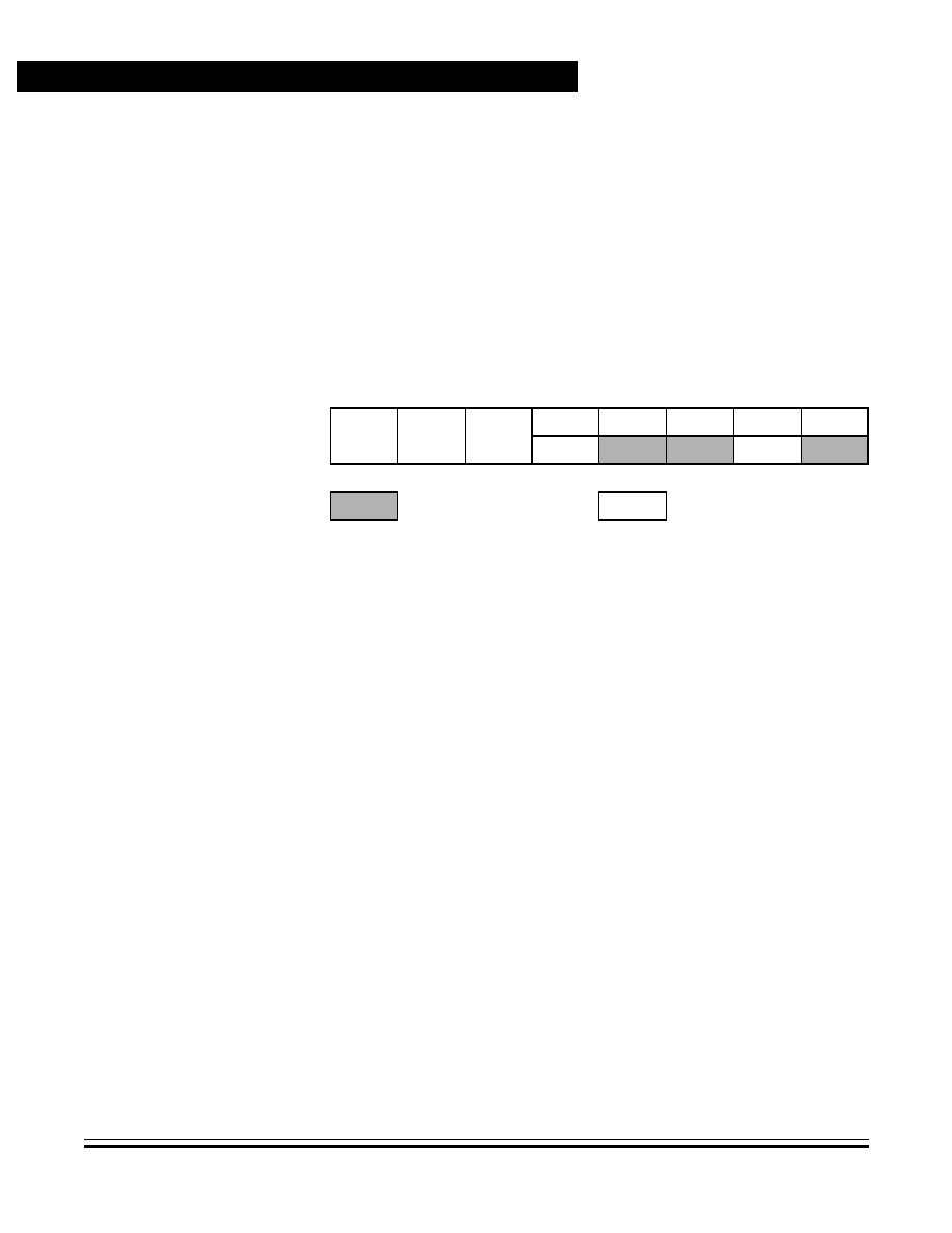
Advance Information
MC68HC705JJ7 ∑ MC68HC705JP7 -- REV 4
76
Operating Modes
MOTOROLA
Operating Modes
6.3 Oscillator Source
The microcontroller unit (MCU) can be clocked by either an internal
low-power oscillator (LPO) without external components or by an
external pin oscillator (EPO) which uses external components. The
enable and selection of the clock source is determined by the state of the
oscillator select bits (OM1 and OM2) in the interrupt status and control
register (ISCR) as shown in
Figure 6-1
.
IRQE -- External Interrupt Request Enable Bit
This read/write bit enables external interrupts. Refer to
Section 4.
Interrupts
for more details.
OM1 and OM2 -- Oscillator Select Bits
These bits control the selection and enabling of the oscillator source
for the MCU. One choice is the internal LPO and the other oscillator
is the EPO which is common to most M68HC05 MCU devices. The
EPO uses external components like filter capacitors and a crystal or
ceramic resonator and consumes more power than the LPO. The
selection and enable conditions for these two oscillators are shown in
Table 6-1
. Reset clears OM1 and sets OM2, which selects the LPO
and disables the EPO.
Therefore, the lowest power is consumed when OM1 is cleared. The
state with both OM1 and OM2 set is provided so that the EPO can be
started up and allowed to stabilize while the LPO still clocks the MCU.
Address:
$000D
Bit 7
6
5
4
3
2
1
Bit 0
Read:
IRQE
OM2
OM1
0
IRQF
0
0
0
Write:
R
IRQR
Reset:
1
1
0
0
0
0
0
0
= Unimplemented
R
= Reserved
Figure 6-1. IRQ Status and Control Register (ISCR)

Operating Modes
Low-Power Modes
MC68HC705JJ7 ∑ MC68HC705JP7 -- REV 4
Advance Information
MOTOROLA
Operating Modes
77
.
NOTE:
When switching from LPO to EPO, the user must be careful to ensure
that the EPO has been enabled and powered up long enough to stabilize
before shifting clock sources.
IRQF -- External Interrupt Request Flag
The IRQF flag is a clearable, read-only bit that is set when an external
interrupt request is pending. Refer to
Section 4. Interrupts
for more
details.
IRQR -- Interrupt Request Reset Bit
This write-only bit clears the IRQF flag bit and prevents redundant
execution of interrupt routines. Refer to
Section 4. Interrupts
for
more details.
6.4 Low-Power Modes
Four modes of operation reduce power consumption:
∑
Stop mode
∑
Wait mode
∑
Halt mode
∑
Data-retention mode
Figure 6-2
shows the sequence of events in stop, wait, and halt modes.
Table 6-1. Oscillator Selection
OM2
OM1
Oscillator
Selected
Internal
Low-Power
Oscillator
(LPO)
External Pin
Oscillator
(EPO)
Power
Consumption
0
0
Internal
Enabled
Disabled
Lowest
0
1
External
Disabled
Enabled
Normal
1
0
Internal
Enabled
Disabled
Lowest
1
1
Internal
Enabled
Enabled
Normal
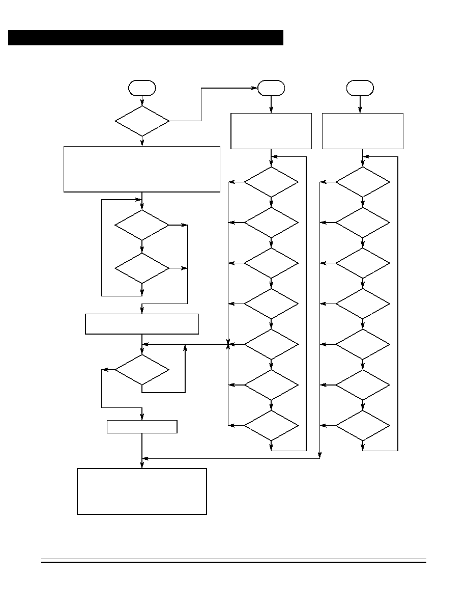
Advance Information
MC68HC705JJ7 ∑ MC68HC705JP7 -- REV 4
78
Operating Modes
MOTOROLA
Operating Modes
Figure 6-2. Stop/Wait/Halt Flowchart
STOP
SWAIT BIT
IN MOR SET?
CLEAR I BIT IN CCR.
SET IRQE BIT IN ISCR.
CLEAR CTOF, RTIF, CTOFE, AND RTIE BITS IN TSCR.
DISABLE EXTERNAL PIN OSCILLATOR.
EXTERNAL
RESET?
EXTERNAL
INTERRUPT?
NO
NO
NO
TURN ON SELECTED OSCILLATOR.
RESET STABILIZATION DELAY TIMER.
YES
YES
HALT
YES
END OF
STABILIZATION
DELAY?
YES
NO
NO
EXTERNAL
RESET?
CLEAR I BIT IN CCR.
SET IRQE BIT IN ISCR.
TURN OFF CPU CLOCK.
KEEP OTHER MODULE
YES
WAIT
TURN ON CPU CLOCK.
1. LOAD PC WITH RESET VECTOR
OR
2. SERVICE INTERRUPT.
a. SAVE CPU REGISTERS ON STACK.
b. SET I BIT IN CCR.
c. LOAD PC WITH INTERRUPT VECTOR.
TURN OFF INTERNAL LOW-POWER OSCILLATOR.
CLEAR ICF, OCF, AND TOF BITS IN TSR.
CLEAR ICIE, OCIE, AND TOIE BITS IN TCR.
CLOCKS ACTIVE.
NO
CORE
INTERRUPT?
YES
TIMER
NO
EXTERNAL
INTERRUPT?
YES
NO
PROG.
INTERRUPT?
YES
TIMER
NO
SIOP
INTERRUPT?
YES
NO
INTERRUPT?
YES
ANALOG
NO
COP
RESET?
YES
CLEAR I BIT IN CCR.
SET IRQE BIT IN ISCR.
TURN OFF CPU CLOCK.
KEEP OTHER MODULE
CLOCKS ACTIVE.
NO
EXTERNAL
RESET?
YES
NO
CORE
INTERRUPT?
YES
TIMER
NO
EXTERNAL
INTERRUPT?
YES
NO
PROG.
INTERRUPT?
YES
TIMER
NO
SIOP
INTERRUPT?
YES
NO
YES
NO
COP
RESET?
YES
INTERRUPT?
ANALOG

Operating Modes
Low-Power Modes
MC68HC705JJ7 ∑ MC68HC705JP7 -- REV 4
Advance Information
MOTOROLA
Operating Modes
79
6.4.1 Stop Mode
The STOP instruction puts the MCU in a mode with the lowest power
consumption and affects the MCU as follows:
∑
Turns off the central processor unit (CPU) clock and all internal
clocks by stopping both the external pin oscillator and the internal
low-power oscillator. The selection of the oscillator by the OM1
and OM2 bits in the ISCR is not affected. The stopped clocks turn
off the COP watchdog, the core timer, the programmable timer,
the analog subsystem, and the SIOP.
∑
Removes any pending core timer interrupts by clearing the core
timer interrupt flags (CTOF and RTIF) in the core timer status and
control register (CTSCR)
∑
Disables any further core timer interrupts by clearing the core
timer interrupt enable bits (CTOFE and RTIE) in the CTSCR
∑
Removes any pending programmable timer interrupts by clearing
the timer interrupt flags (ICF, OCF, and TOF) in the timer status
register (TSR)
∑
Disables any further programmable timer interrupts by clearing the
timer interrupt enable bits (ICIE, OCIE, and TOIE) in the timer
control register (TCR)
∑
Enables external interrupts via the IRQ/V
PP
pin by setting the
IRQE bit in the IRQ status and control register (ISCR). External
interrupts are also enabled via the PA0 through PA3 pins, if the
port A interrupts are enabled by the PIRQ bit in the mask option
register (MOR).
∑
Enables interrupts in general by clearing the I bit in the condition
code register
The STOP instruction does not affect any other bits, registers, or I/O
lines.

Advance Information
MC68HC705JJ7 ∑ MC68HC705JP7 -- REV 4
80
Operating Modes
MOTOROLA
Operating Modes
The following conditions bring the MCU out of stop mode:
∑
An external interrupt signal on the IRQ/V
PP
pin -- A high-to-low
transition on the IRQ/V
PP
pin loads the program counter with the
contents of locations $1FFA and $1FFB.
∑
An external interrupt signal on a port A external interrupt pin -- If
selected by the PIRQ bit in the MOR, a low-to-high transition on a
PA3≠PA0 pin loads the program counter with the contents of
locations $1FFA and $1FFB.
∑
External reset -- A logic 0 on the RESET pin resets the MCU and
loads the program counter with the contents of locations $1FFE
and $1FFF.
When the MCU exits stop mode, processing resumes after a
stabilization delay of 16 or 4064 internal bus cycles, depending on the
state of the DELAY bit in the MOR.
NOTE:
Execution of the STOP instruction without setting the SWAIT bit in the
MOR will cause the oscillators to stop, and, therefore, disable the COP
watchdog timer. If the COP watchdog timer is to be used, stop mode
should be changed to halt mode as described in
6.4.3 Halt Mode
.
6.4.2 Wait Mode
The WAIT instruction puts the MCU in a low-power wait mode which
consumes more power than the stop mode and affects the MCU as
follows:
∑
Enables interrupts by clearing the I bit in the condition code
register
∑
Enables external interrupts by setting the IRQE bit in the IRQ
status and control register
∑
Stops the CPU clock which drives the address and data buses, but
allows the selected oscillator to continue to clock the core timer,
programmable timer, analog subsystem, and SIOP
The WAIT instruction does not affect any other bits, registers, or I/O
lines.

Operating Modes
Low-Power Modes
MC68HC705JJ7 ∑ MC68HC705JP7 -- REV 4
Advance Information
MOTOROLA
Operating Modes
81
These conditions restart the CPU bus clock and bring the MCU out of
wait mode:
∑
An external interrupt signal on the IRQ/V
PP
pin -- A high-to-low
transition on the IRQ/V
PP
pin loads the program counter with the
contents of locations $1FFA and $1FFB.
∑
An external interrupt signal on a port A external interrupt pin -- If
selected by PIRQ bit in the MOR, a low-to-high transition on a
PA3≠PA0 pin loads the program counter with the contents of
locations $1FFA and $1FFB.
∑
A core timer interrupt -- A core timer overflow or a real-time
interrupt loads the program counter with the contents of locations
$1FF8 and $1FF9.
∑
A programmable timer interrupt -- A programmable timer interrupt
driven by an input capture, output compare, or timer overflow
loads the program counter with the contents of locations $1FF6
and $1FF7.
∑
An SIOP interrupt -- An SIOP interrupt driven by the completion
of transmitted or received 8-bit data loads the program counter
with the contents of locations $1FF4 and $1FF5.
∑
An analog subsystem interrupt -- An analog subsystem interrupt
driven by a voltage comparison loads the program counter with
the contents of locations $1FF2 and $1FF3.
∑
A COP watchdog reset -- A timeout of the COP watchdog resets
the MCU and loads the program counter with the contents of
locations $1FFE and $1FFF. Software can enable real-time
interrupts so that the MCU can periodically exit the wait mode to
reset the COP watchdog.
∑
An external reset -- A logic 0 on the RESET pin resets the MCU
and loads the program counter with the contents of locations
$1FFE and $1FFF.
When the MCU exits the wait mode, there is no delay before code
executes like occurs when exiting the stop or halt modes.

Advance Information
MC68HC705JJ7 ∑ MC68HC705JP7 -- REV 4
82
Operating Modes
MOTOROLA
Operating Modes
6.4.3 Halt Mode
The STOP instruction puts the MCU in halt mode if selected by the
SWAIT bit in the MOR. Halt mode is identical to wait mode, except that
a variable recovery delay occurs when the MCU exits halt mode. A
recovery time of from 1 to 16 or from 1 to 4064 internal bus cycles can
be selected by the DELAY bit in the MOR.
If the SWAIT bit is set in the MOR to put the MCU in halt mode, the COP
watchdog cannot be turned off inadvertently by a STOP instruction.
6.4.4 Data-Retention Mode
In the data-retention mode, the MCU retains random-access memory
(RAM) contents and CPU register contents at V
DD
voltages as low as 2.0
Vdc. The data retention feature allows the MCU to remain in a low-power
consumption state during which it retains data, but the CPU cannot
execute instructions. Current consumption in this mode is not tested.
To put the MCU in the data retention mode:
1. Drive the RESET pin to a logic 0.
2. Lower the V
DD
voltage. The RESET pin must remain low
continuously during data retention mode.
To take the MCU out of the data retention mode:
1. Return V
DD
to normal operating voltage.
2. Return the RESET pin to a logic 1.

MC68HC705JJ7 ∑ MC68HC705JP7 -- REV 4
Advance Information
MOTOROLA
Parallel Input/Output
83
Advance Information -- MC68HC705JJ7/MC68HC705JP7
Section 7. Parallel Input/Output
7.1 Contents
7.2
Introduction . . . . . . . . . . . . . . . . . . . . . . . . . . . . . . . . . . . . . . . . 84
7.3
Port A . . . . . . . . . . . . . . . . . . . . . . . . . . . . . . . . . . . . . . . . . . . . 84
7.3.1
Port A Data Register . . . . . . . . . . . . . . . . . . . . . . . . . . . . . . 85
7.3.2
Data Direction Register A. . . . . . . . . . . . . . . . . . . . . . . . . . . 86
7.3.3
Pulldown Register A . . . . . . . . . . . . . . . . . . . . . . . . . . . . . . . 87
7.3.4
Port A External Interrupts . . . . . . . . . . . . . . . . . . . . . . . . . . . 88
7.3.5
Port A Logic . . . . . . . . . . . . . . . . . . . . . . . . . . . . . . . . . . . . . 89
7.4
Port B . . . . . . . . . . . . . . . . . . . . . . . . . . . . . . . . . . . . . . . . . . . . 90
7.4.1
Port B Data Register . . . . . . . . . . . . . . . . . . . . . . . . . . . . . . 90
7.4.2
Data Direction Register B. . . . . . . . . . . . . . . . . . . . . . . . . . . 91
7.4.3
Pulldown Register B . . . . . . . . . . . . . . . . . . . . . . . . . . . . . . . 92
7.4.4
Port B Logic . . . . . . . . . . . . . . . . . . . . . . . . . . . . . . . . . . . . . 92
7.4.5
PB0, PBI, PB2, and PB3 Logic. . . . . . . . . . . . . . . . . . . . . . .93
7.4.6
PB4/AN4/TCMP/CMP1 Logic. . . . . . . . . . . . . . . . . . . . . . . . 94
7.4.7
PB5/SDO Logic . . . . . . . . . . . . . . . . . . . . . . . . . . . . . . . . . .96
7.4.8
PB6/SDI Logic . . . . . . . . . . . . . . . . . . . . . . . . . . . . . . . . . . . 98
7.4.9
PB7/SCK Logic. . . . . . . . . . . . . . . . . . . . . . . . . . . . . . . . . . . 99
7.5
Port C (28-Pin Versions Only) . . . . . . . . . . . . . . . . . . . . . . . . 101
7.5.1
Port C Data Register . . . . . . . . . . . . . . . . . . . . . . . . . . . . . 102
7.5.2
Data Direction Register C. . . . . . . . . . . . . . . . . . . . . . . . . . 102
7.5.3
Port C Pulldown Devices . . . . . . . . . . . . . . . . . . . . . . . . . .103
7.5.4
Port C Logic . . . . . . . . . . . . . . . . . . . . . . . . . . . . . . . . . . . . 103
7.6
Port Transitions. . . . . . . . . . . . . . . . . . . . . . . . . . . . . . . . . . . .105

Advance Information
MC68HC705JJ7 ∑ MC68HC705JP7 -- REV 4
84
Parallel Input/Output
MOTOROLA
Parallel Input/Output
7.2 Introduction
The MC68HC705JJ7 has 14 bidirectional input/output (I/O) pins which
form two parallel I/O ports, A and B. The MC68HC705JP7 has
22 bidirectional I/O pins which form three parallel I/O ports, A, B and C.
Each I/O pin is programmable as an input or an output. The contents of
the data direction registers determine the data direction of each of the
I/O pins. All I/O pins have software programmable pulldown devices
which can be enabled or disabled globally by the SWPDI bit in the mask
option register (MOR).
7.3 Port A
Port A is a 6-bit, general-purpose, bidirectional I/O port with these
features:
∑
Individual programmable pulldown devices
∑
High current sinking capability on all port A pins, with a maximum
total for port A
∑
High current sourcing capability on all port A pins, with a maximum
total for port A
∑
External interrupt capability (pins PA3≠PA0)

Parallel Input/Output
Port A
MC68HC705JJ7 ∑ MC68HC705JP7 -- REV 4
Advance Information
MOTOROLA
Parallel Input/Output
85
7.3.1 Port A Data Register
The port A data register (PORTA) contains a bit for each of the port A
pins. When a port A pin is programmed to be an output, the state of its
data register bit determines the state of the output pin. When a port A pin
is programmed to be an input, reading the port A data register returns
the logic state of the pin. The upper two bits of the port A data register
will always read as logic 0s.
PA5≠PA0 -- Port A Data Bits
These read/write bits are software programmable. Data direction of
each bit is under the control of the corresponding bit in the port A data
direction register (DDRA). Reset has no effect on port A data.
Address:
$0000
Bit 7
6
5
4
3
2
1
Bit 0
Read:
0
0
PA5
PA4
PA3
PA2
PA1
PA0
Write:
Reset:
Unaffected by reset
Alternate:
KYBD3
KYBD2
KYBD1
KYBD0
= Unimplemented
Figure 7-1. Port A Data Register (PORTA)
Advance Information
MC68HC705JJ7 ∑ MC68HC705JP7 -- REV 4
86
Parallel Input/Output
MOTOROLA
Parallel Input/Output
7.3.2 Data Direction Register A
The contents of the port A data direction register (DDRA) determine
whether each port A pin is an input or an output. Writing a logic 1 to a
DDRA bit enables the output buffer for the associated port A pin. A
DDRA bit set to a logic 1 also disables the pulldown device for that pin.
Writing a logic 0 to a DDRA bit disables the output buffer for the
associated port A pin. The upper two bits always read as logic 0s. A reset
initializes all DDRA bits to logic 0s, configuring all port A pins as inputs
and disabling the voltage comparators from driving PA4 or PA5.
DDRA5≠DDRA0 -- Port A Data Direction Bits
These read/write bits control port A data direction. Reset clears the
DDRA5≠DDRA0 bits.
1 = Corresponding port A pin configured as output and pulldown
device disabled
0 = Corresponding port A pin configured as input
Address:
$0004
Bit 7
6
5
4
3
2
1
Bit 0
Read:
0
0
DDRA5
DDRA4
DDRA3
DDRA2
DDRA1
DDRA0
Write:
Reset:
0
0
0
0
0
0
0
0
= Unimplemented
Figure 7-2. Data Direction Register A (DDRA)

Parallel Input/Output
Port A
MC68HC705JJ7 ∑ MC68HC705JP7 -- REV 4
Advance Information
MOTOROLA
Parallel Input/Output
87
7.3.3 Pulldown Register A
All port A pins can have software programmable pulldown devices
enabled or disabled globally by SWPDI bit in the MOR. These pulldown
devices are controlled by the write-only pulldown register A (PDRA)
shown in
Figure 7-3
. Clearing the PDIA5≠PDIA0 bits in the PDRA turns
on the pulldown devices if the port A pin is an input. Reading the PDRA
returns undefined results since it is a write-only register; therefore, do
not change the value in PDRA with read/modify/write instructions. On
the MC68HC705JP7 the PDRA contains two pulldown control bits
(PDICH and PDICL) for port C. Reset clears the PDIA5≠PDIA0, PDICH,
and PDICL bits, which turns on all the port A and port C pulldown
devices.
PDICH -- Upper Port C Pulldown Inhibit Bits (MC68HC705JP7)
Writing to this write-only bit controls the port C pulldown devices on
the upper four bits (PC4≠PC7). Reading these pulldown register A
bits returns undefined data. Reset clears bit PDICH.
1 = Upper four port C pins pulldown devices turned off
0 = Upper four port C pins pulldown devices turned on if pin has
been programmed by the DDRC to be an input
PDICL -- Lower Port C Pulldown Inhibit Bits (MC68HC705JP7)
Writing to this write-only bit controls the port C pulldown devices on
the lower four bits (PC0≠PC3). Reading these pulldown register A bits
returns undefined data. Reset clears bit PDICL.
1 = Lower four port C pins pulldown devices turned off
Address:
$0010
Bit 7
6
5
4
3
2
1
Bit 0
Read:
Write:
PDICH
PDICL
PDIA5
PDIA4
PDIA3
PDIA2
PDIA1
PDIA0
Reset:
0
0
0
0
0
0
0
0
= Unimplemented
Figure 7-3. Pulldown Register A (PDRA)

Advance Information
MC68HC705JJ7 ∑ MC68HC705JP7 -- REV 4
88
Parallel Input/Output
MOTOROLA
Parallel Input/Output
0 = Lower four port C pins pulldown devices turned on if pin has
been programmed by the DDRC to be an input
PDIA5≠PDIA0 -- Port A Pulldown Inhibit Bits
Writing to these write-only bits controls the port A pulldown devices.
Reading these pulldown register A bits returns undefined data. Reset
clears bits PDIA5≠PDIA0.
1 = Corresponding port A pin pulldown device turned off
0 = Corresponding port A pin pulldown device turned on if pin has
been programmed by the DDRA to be an input
7.3.4 Port A External Interrupts
The PIRQ bit in the MOR enables the PA3≠PA0 pins to serve as external
interrupt pins in addition to the IRQ/V
PP
pin. The active interrupt state for
the PA3≠PA0 pins is a logic 1 or a rising edge. A state of the PIRQ bit in
the MOR determines whether external interrupt inputs are
edge-sensitive only or both edge- and level-sensitive. Port A interrupts
are also interactive with each other and the IRQ/V
PP
pin as described in
4.6 External Interrupts
.
NOTE:
When testing for external interrupts, the BIH and BIL instructions test the
voltage on the IRQ/V
PP
pin, not the state of the internal IRQ signal.
Therefore, BIH and BIL cannot test the port A external interrupt pins.
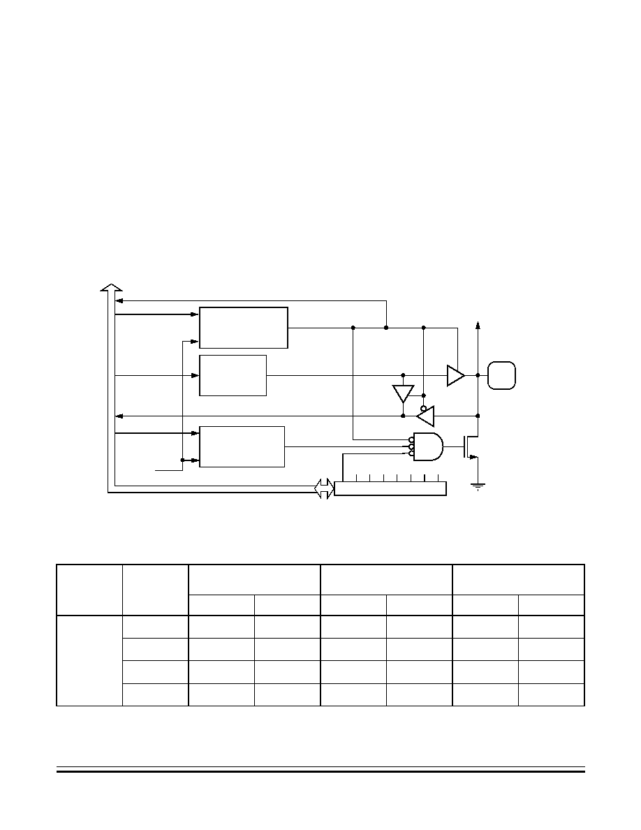
Parallel Input/Output
Port A
MC68HC705JJ7 ∑ MC68HC705JP7 -- REV 4
Advance Information
MOTOROLA
Parallel Input/Output
89
7.3.5 Port A Logic
When a PA0:PA5 pin is programmed as an output, reading the port bit
actually reads the value of the data latch and not the voltage on the pin
itself. When a PA0:PA5 pin is programmed as an input, reading the port
bit reads the voltage level on the pin. The data latch can always be
written, regardless of the state of its DDR bit.
Figure 7-4
shows the I/O
logic of PA0≠PA5 pins of port A.
The data latch can always be written, regardless of the state of its DDR
bits.
Table 7-1
summarizes the operations of the port A pins.
Figure 7-4. Port A I/O Circuit
PAx
EXTERNAL
INTERRUPT
REQUEST
PORT A DATA
REGISTER
BIT PAx
READ $0004
WRITE $0000
READ $0000
WRITE $0010
PULLDOWN
DEVICE
RESET
INT
E
R
N
A
L
D
A
T
A
BUS
HIGH SINK/SOURCE
CURRENT
SW
PD
I
WRITE $0004
DATA DIRECTION
REGISTER A
BIT DDRAx
PULLDOWN
REGISTER A
BIT PDIAx
R
R
MASK OPTION REG. ($1FF1)
CAPABILITY
(PA0:3)
Table 7-1. Port A Pin Functions
Port A
Pin(s)
SWPDI
(in MOR)
Port A
PORTA Access
(Pin or Data Register)
Result on
Port A Pins
PDIAx
DDRAx
(1)
Read
Write
Pulldown
Pin
PA0
PA1
PA2
PA3
PA4
PA5
0
0
0
Pin
Data
On
PAx in
0
1
0
Pin
Data
Off
PAx in
1
X
0
Pin
Data
Off
PAx in
X
(2)
X
(2)
1
Data
Data
Off
PAx out
1. DDRA can always be read or written.
2. Don't care

Advance Information
MC68HC705JJ7 ∑ MC68HC705JP7 -- REV 4
90
Parallel Input/Output
MOTOROLA
Parallel Input/Output
7.4 Port B
Port B is an 8-bit, general-purpose, bidirectional I/O port with these
features:
∑
Programmable pulldown devices
∑
PB0≠PB4 are shared with the analog subsystem.
∑
PB3 and PB4 are shared with the 16-bit programmable timer.
∑
PB4 can be driven directly by the output of comparator 1.
∑
PB5≠PB7 are shared with the simple serial interface (SIOP).
∑
High current sinking capability on the PB4 pin
∑
High current sourcing capability on the PB4 pin
7.4.1 Port B Data Register
The port B data register (PORTB) contains a bit for each of the port B
pins. When a port B pin is programmed to be an output, the state of its
data register bit determines the state of the output pin. When a port B pin
is programmed to be an input, reading the port B data register returns
the logic state of the pin. Reset has no effect on port B data.
PB0-PB7 -- Port B Data Bits
These read/write bits are software programmable. Data direction of
each bit is under the control of the corresponding bit in data direction
register B. Reset has no effect on port B data.
Address:
$0001
Bit 7
6
5
4
3
2
1
Bit 0
Read:
PB7
PB6
PB5
PB4
PB3
PB2
PB1
PB0
Write:
Reset:
Unaffected by reset
Alternate:
SCK
SDI
SDO
AN4
AN3
AN2
AN1
AN0
Alternate:
SCK
SDI
SDO
TCMP
TCAP
AN2
AN1
AN0
Alternate:
SCK
SDI
SDO
CMP1
TCAP
AN2
AN1
AN0
Figure 7-5. Port B Data Register (PORTB)

Parallel Input/Output
Port B
MC68HC705JJ7 ∑ MC68HC705JP7 -- REV 4
Advance Information
MOTOROLA
Parallel Input/Output
91
7.4.2 Data Direction Register B
The contents of the port B data direction register (DDRB) determine
whether each port B pin is an input or an output. Writing a logic 1 to a
DDRB bit enables the output buffer for the associated port B pin. A
DDRB bit set to a logic 1 also disables the pulldown device for that pin.
Writing a logic 0 to a DDRB bit disables the output buffer for the
associated port B pin. A reset initializes all DDRB bits to logic 0s,
configuring all port B pins as inputs.
DDRB7≠DDRB0 -- Port B Data Direction Bits
These read/write bits control port B data direction. Reset clears the
bits DDRB7≠DDRB0.
1 = Corresponding port B pin configured as output and pulldown
device disabled
0 = Corresponding port B pin configured as input
Address:
$0005
Bit 7
6
5
4
3
2
1
Bit 0
Read:
DDRB7
DDRB6
DDRB5
DDRB4
DDRB3
DDRB2
DDRB1
DDRB0
Write:
Reset:
0
0
0
0
0
0
0
0
Figure 7-6. Data Direction Register B (DDRB)

Advance Information
MC68HC705JJ7 ∑ MC68HC705JP7 -- REV 4
92
Parallel Input/Output
MOTOROLA
Parallel Input/Output
7.4.3 Pulldown Register B
All port B pins can have software programmable pulldown devices
enabled or disabled globally by the SWPDI bit in the MOR. These
pulldown devices are individually controlled by the write-only pulldown
register B (PDRB) shown in
Figure 7-7
. Clearing the PDIB7≠PDIB0 bits
in the PDRB turns on the pulldown devices if the port B pin is an input.
Reading the PDRB returns undefined results since it is a write-only
register. Reset clears the PDIB7≠PDIB0 bits, which turns on all the port
B pulldown devices.
PDIB7≠PDIB0 -- Port B Pulldown Inhibit Bits
Writing to these write-only bits controls the port B pulldown devices.
Reading these pulldown register B bits returns undefined data. Reset
clears bits PDIB7≠PDIB0.
1 = Corresponding port B pin pulldown device turned off
0 = Corresponding port B pin pulldown device turned on if pin has
been programmed by the DDRB to be an input
7.4.4 Port B Logic
All port B pins have the general I/O port logic similar to port A; but they
also share this function with inputs or outputs from other modules, which
are also attached to the pin itself or override the general I/O function.
PB0, PB1, PB2, and PB3 simply share their inputs with another module.
PB4, PB5, PB6, and PB7 will have their operation altered by outputs or
controls from other modules.
Address:
$0011
Bit 7
6
5
4
3
2
1
Bit 0
Read:
Write:
PDIB7
PDIB6
PDIB5
PDIB4
PDIB3
PDIB2
PDIB1
DIB0
Reset:
0
0
0
0
0
0
0
0
= Unimplemented
Figure 7-7. Pulldown Register B (PDRB)

Parallel Input/Output
Port B
MC68HC705JJ7 ∑ MC68HC705JP7 -- REV 4
Advance Information
MOTOROLA
Parallel Input/Output
93
7.4.5 PB0, PBI, PB2, and PB3 Logic
The typical I/O logic shown in
Figure 7-8
is used for PB0, PB1, PB2, and
PB3 pins of port B. When these port B pins are programmed as an
output, reading the port bit actually reads the value of the data latch and
not the voltage on the pin itself. When these port B pins are programmed
as an input, reading the port bit reads the voltage level on the pin. The
data latch can always be written, regardless of the state of its DDRB bit.
The operations of the PB0≠PB3 pins are summarized in
Table 7-2
.
Figure 7-8. PB0≠PB3 Pin I/O Circuit
The PB0≠PB3 pins share their inputs with another module. When using
the other attached module, these conditions must be observed:
1. If the DDRB configures the pin as an output, then the port data
register can provide an output which may conflict with any external
input source to the other module. The pulldown device will be
disabled in this case.
2. If the DDRB configures the pin as an input, then reading the port
data register will return the state of the input in terms of the digital
threshold for that pin (analog inputs will default to logic states).
3. If DDRB configures the pin as an input and the pulldown device is
activated for a pin, it will also load the input to the other module.
PORT BDATA
REGISTER
BIT PBx
DATA DIRECTION
REGISTER B
BIT DDRBx
PULLDOWN
REGISTER B
BIT PDIBx
R
R
PBx
ANALOG SUBSYSTEM,
AND PROGRAMMABLE
TIMER INPUT CAPTURE
READ $0005
WRITE $0001
READ $0001
WRITE $0011
PULLDOWN
DEVICE
RESET
IN
TE
RN
AL D
A
T
A
B
U
S
(PINS PB0, PB1, PB2, PB3)
WRITE $0005
SW
PD
I
MASK OPTION REG. ($1FF1)
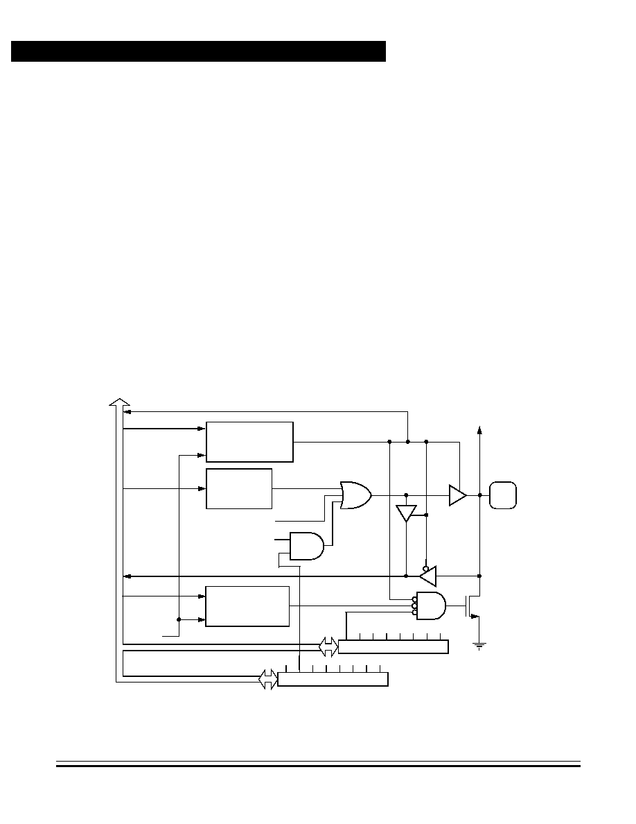
Advance Information
MC68HC705JJ7 ∑ MC68HC705JP7 -- REV 4
94
Parallel Input/Output
MOTOROLA
Parallel Input/Output
4. If interaction between the port logic and the other module is not
desired, the pin should be configured as an input by clearing the
appropriate DDRB bit. The input pulldown device is disabled by
clearing the appropriate PDRB bit (or by disabling programmable
pulldowns with the SWPDI bit in the MOR).
7.4.6 PB4/AN4/TCMP/CMP1 Logic
The PB4/AN4/TCMP/CMP1 pin can be used as a simple I/O port pin, be
controlled by the OLVL bit from the output compare function of the 16-bit
programmable timer, or be controlled directly by the output of
comparator 1 as shown in
Figure 7-9
. The PB4 data, the programmable
timer OLVL bit, and the output of comparator 1 are all logically ORed
together to drive the pin. Also, the analog subsystem input channel 4
multiplexer is connected directly to this pin. The operations of PB4 pin
are summarized in
Table 7-2
.
Figure 7-9. PB4/AN4/TCMP/CMP1 Pin I/O Circuit
PORT BDATA
REGISTER
BIT PB4
DATA DIRECTION
REGISTER B
BIT DDRB4
PULLDOWN
REGISTER B
BIT PDIB4
R
R
PB4
ANALOG SUBSYSTEM
INPUT AN4 AND
TIMER OUTPUT COMPARE
READ $0005
WRITE $0001
READ $0001
WRITE $0011
PULLDOWN
DEVICE
RESET
I
N
T
E
RN
AL
D
A
T
A
BUS
WRITE $0005
AN4
TCMP
OLVL
SW
PD
I
MASK OPTION REG. ($1FF1)
CMP1
(COMPARATOR 1 OUT)
(TIMER OUTPUT COMPARE)
OP
T
COP REGISTER ($1FF0)
HIGH SINK/
SOURCE CURRENT
CAPABILITY

Parallel Input/Output
Port B
MC68HC705JJ7 ∑ MC68HC705JP7 -- REV 4
Advance Information
MOTOROLA
Parallel Input/Output
95
When using the PB4/AN4/TCMP/CMP1 pin, these interactions must be
noted:
1. If the OLVL timer output compare function is the required output
function, then the DDRB4 bit must be set, the PB4 data bit must
be cleared, and the OPT bit in the COPR must be cleared. The
PB4/AN4/TCMP/CMP1 pin becomes an output which follows the
state of the OLVL bit. The pulldown device will be disabled in this
case. The analog subsystem would not normally use this pin as an
analog input in this case.
2. If the PB4 data bit is the required output function, then the DDRB4
bit must be set, the OLVL bit in the TCR must be cleared, and the
OPT bit in the COPR must be cleared. The pulldown device will be
disabled in this case. The analog subsystem would not normally
use this pin as an analog input in this case.
3. If the comparator 1 output is the desired output function, then the
PB4 data bit must be cleared, the DDRB4 bit must be set, the
OLVL bit in the TCR must be cleared, and the OPT bit in the
COPR must be set. The PB4/AN4/TCMP/CMP1 pin becomes an
output which follows the state of the OLVL bit. The pulldown
device will be disabled in this case. The analog subsystem would
not normally use this pin as an analog input in this case.
4. If the PB4 pin is to be an input to the analog subsystem or a digital
input, then the DDRB4 bit must be cleared. In this case, the PB4
pin can still be read, but the voltage present will be returned as a
binary value. Depending on the external application, the PB4
pulldown may also be disabled by setting the PDIB4 pulldown
inhibit bit. In this case, both the digital and analog functions
connected to this pin can be utilized.
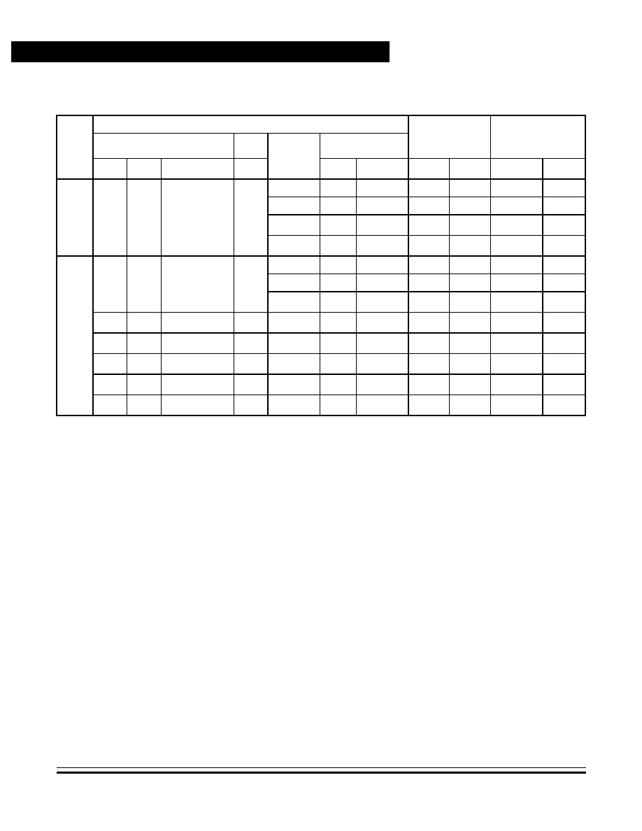
Advance Information
MC68HC705JJ7 ∑ MC68HC705JP7 -- REV 4
96
Parallel Input/Output
MOTOROLA
Parallel Input/Output
.
7.4.7 PB5/SDO Logic
The PB5/SDO pin can be used as a simple I/O port pin or be controlled
by the SIOP serial interface as shown in
Figure 7-10
. The operations of
the PB5 pin are summarized in
Table 7-3
.
When using the PB5/SDO pin, these interactions must be noted:
1. If the SIOP function is required, then the SPE bit in the SCR must
be set. This causes the PB5/SDO pin buffer to be enabled and to
be driven by the serial data output (SDO) from the SIOP. The
pulldown device will be disabled in this case.
2. If the SIOP function is in control of the PB5/SDO pin, the DDRB5
and PB5 data register bits are still accessible to the CPU and can
be altered or read without affecting the SIOP functionality.
However, if the DDRB5 bit is cleared, reading the PB5 data
register will return the current state of the PB5/SDO pin.
Table 7-2. Port B Pin Functions -- PB0≠PB4
Port B
Pin
Control Bits
PORTB Access
(Pin or Data
Register)
Result on
Port B Pins
Comparator 1
Timer
SWPDI
in MOR
Port B
CMP1 COE1 OPT in COPR OLVL
PDIBx DDRBx
(1)
Read
Write
Pulldown
Pin
PB0
PB1
PB2
PB3
X
(2)
X
(2)
X
(2)
X
(2)
0
0
0
Pin
Data
On
PBx in
0
1
0
Pin
Data
Off
PBx in
1
X
(2)
0
Pin
Data
Off
PBx in
X
(2)
X
(2)
1
Data
Data
Off
PBx out
PB4
X
(2)
X
(2)
X
(2)
X
(2)
0
0
0
Pin
Data
On
PB4 in
0
1
0
Pin
Data
Off
PB4 in
1
X
(2)
0
Pin
Data
Off
PB4 in
X
(2)
X
(2)
0
0
X
(2)
X
(2)
1
Data
Data
Off
PB4 out
X
(2)
0
1
0
X
(2)
X
(2)
1
Data
Data
Off
PB4 out
0
1
1
0
X
(2)
X
(2)
1
Data
Data
Off
PB4 out
X
(2)
X
(2)
X
(2)
1
X
(2)
X
(2)
1
1
Data
Off
1
1
1
1
X
(2)
X
(2)
X
(2)
1
1
Data
Off
1
1. DDRB can always be read or written.
2. Don't care
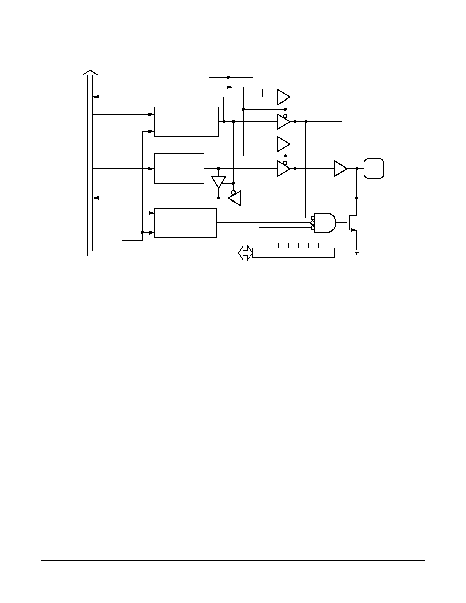
Parallel Input/Output
Port B
MC68HC705JJ7 ∑ MC68HC705JP7 -- REV 4
Advance Information
MOTOROLA
Parallel Input/Output
97
Figure 7-10. PB5/SDO Pin I/O Circuit
3. If the SIOP function is terminated by clearing the SPE bit in the
SCR, then the last conditions stored in the DDRB5, PDIB5, and
PB5 register bits will then control the PB5/SDO pin.
4. If the PB5/SDO pin is to be a digital input, then both the SPE bit in
the SCR and the DDRB5 bit must be cleared. Depending on the
external application, the pulldown device may also be disabled by
setting the PDIB5 pulldown inhibit bit.
5. If the PB5/SDO pin is to be a digital output, then the SPE bit in the
SCR must be cleared and the PDIB5 bit must be set. The pulldown
device will be disabled in this case.
DATA DIRECTION
REGISTER B
BIT DDRB5
PORT B DATA
REGISTER
BIT PB5
PULLDOWN
REGISTER B
BIT PDIB5
R
R
PB5
READ $0005
WRITE $0001
READ $0001
WRITE $0011
PULLDOWN
DEVICE
RESET
INT
E
R
N
AL
D
A
T
A
BUS
WRITE $0005
SDO
SERIAL ENABLE (SPE)
SERIAL DATA OUT (SDO)
V
DD
SW
PD
I
MASK OPTION REG. ($1FF1)
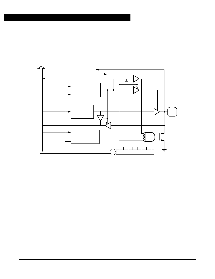
Advance Information
MC68HC705JJ7 ∑ MC68HC705JP7 -- REV 4
98
Parallel Input/Output
MOTOROLA
Parallel Input/Output
7.4.8 PB6/SDI Logic
The PB6/SDI pin can be used as a simple I/O port pin or be controlled
by the SIOP serial interface as shown in
Figure 7-11
. The operations of
PB6/SDI pin are summarized in
Table 7-3
.
Figure 7-11. PB6/SDI Pin I/O Circuit
When using the PB6/SDI pin, these interactions must be noted:
1. If the SIOP function is required, then the SPE bit in the SCR must
be set. This causes the PB6/SDI pin buffer to be disabled to allow
the PB6/SDI pin to act as an input that feeds the serial data input
(SDI) of the SIOP. The pulldown device is disabled in this case.
2. If the SIOP function is in control of the PB6/SDI pin, the DDRB6
and PB6 data register bits are still accessible to the CPU and can
be altered or read without affecting the SIOP functionality.
However, if the DDRB6 bit is cleared, reading the PB6 data
register will return the current state of the PB6/SDI pin.
DATA DIRECTION
REGISTER B
BIT DDRB6
PORT B DATA
REGISTER
BIT PB6
PULLDOWN
REGISTER B
BIT PDIB6
R
R
PB6
READ $0005
WRITE $0001
READ $0001
WRITE $0011
PULLDOWN
DEVICE
RESET
I
N
TE
RN
AL
D
A
T
A
BUS
WRITE $0005
SDI
SERIAL ENABLE (SPE)
SERIAL DATA IN (SDI)
SW
PD
I
MASK OPTION REG. ($1FF1)
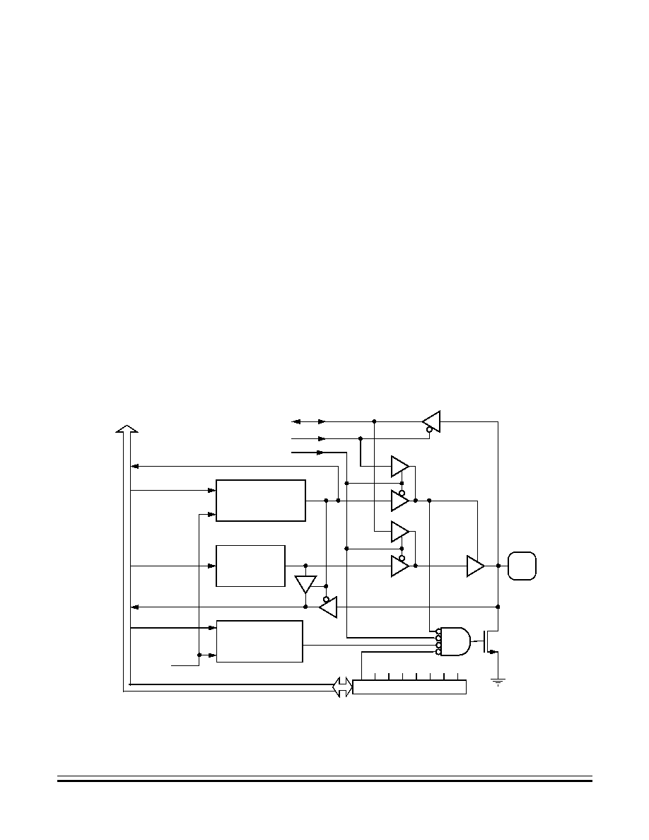
Parallel Input/Output
Port B
MC68HC705JJ7 ∑ MC68HC705JP7 -- REV 4
Advance Information
MOTOROLA
Parallel Input/Output
99
3. If the SIOP function is terminated by clearing the SPE bit in the
SCR, then the last conditions stored in the DDRB6, PDIB6, and
PB6 register bits will then control the PB6/SDI pin.
4. If the PB6/SDI pin is to be a digital input, then both the SPE bit in
the SCR and the DDRB6 bit must be cleared. Depending on the
external application, the pulldown device may also be disabled by
setting the PDIB6 pulldown inhibit bit.
5. If the PB6/SDI pin is to be a digital output, then the SPE bit in the
SCR must be cleared and the DDRB6 bit must be set. The
pulldown device will be disabled in this case.
7.4.9 PB7/SCK Logic
The PB7/SCK pin can be used as a simple I/O port pin or be controlled
by the SIOP serial interface as shown in
Figure 7-12
. The operations of
the PB7/SCK pin are summarized in
Table 7-3
.
Figure 7-12. PB7/SCK Pin I/O Circuit
DATA DIRECTION
REGISTER B
BIT DDRB7
PORT B DATA
REGISTER
BIT PB7
PULLDOWN
REGISTER B
BIT PDIB7
R
R
PB7
READ $0005
WRITE $0001
READ $0001
WRITE $0011
PULLDOWN
DEVICE
RESET
INT
E
R
N
A
L
D
A
T
A
BU
S
WRITE $0005
SCK
SERIAL ENABLE (SPE)
CLOCK SOURCE (MSTR)
SERIAL DATA CLOCK (SCK)
SW
PD
I
MASK OPTION REG. ($1FF1)

Advance Information
MC68HC705JJ7 ∑ MC68HC705JP7 -- REV 4
100
Parallel Input/Output
MOTOROLA
Parallel Input/Output
When using the PB7/SCK pin, these interactions must be noted:
1. If the SIOP function is required, then the SPE bit in the SCR must
be set. This causes the PB7/SCK pin buffer to be controlled by the
MSTR control bit in the SCR. The pulldown device is disabled in
these cases.
a. If the MSTR bit is set, then the PB7/SCK pin buffer will be
enabled and driven by the serial data clock (SCK) from the
SIOP.
b. If the MSTR bit is clear, then the PB7/SCK pin buffer will be
disabled, allowing the PB7/SCK pin to drive the serial data
clock (SCK) into the SIOP.
2. If the SIOP function is in control of the PB7/SCK pin, the DDRB7
and PB7 data register bits are still accessible to the CPU and can
be altered or read without affecting the SIOP functionality.
However, if the DDRB7 bit is cleared, reading the PB7 data
register will return the current state of the PB7/SCK pin.
3. If the SIOP function is terminated by clearing the SPE bit in the
SCR, then the last conditions stored in the DDRB7, PDIB7, and
PB7 register bits will then control the PB7/SCK pin.
4. If the PB7/SCK pin is to be a digital input, then both the SPE bit in
the SCR and the DDRB7 bit must be cleared. Depending on the
external application, the pulldown device may also be disabled by
setting the PDIB7 pulldown inhibit bit.
5. If the PB7/SCK pin is to be a digital output, then the SPE bit in the
SCR must be cleared and the DDRB7 bit must be set. The
pulldown device will be disabled when the pin is set as an output.
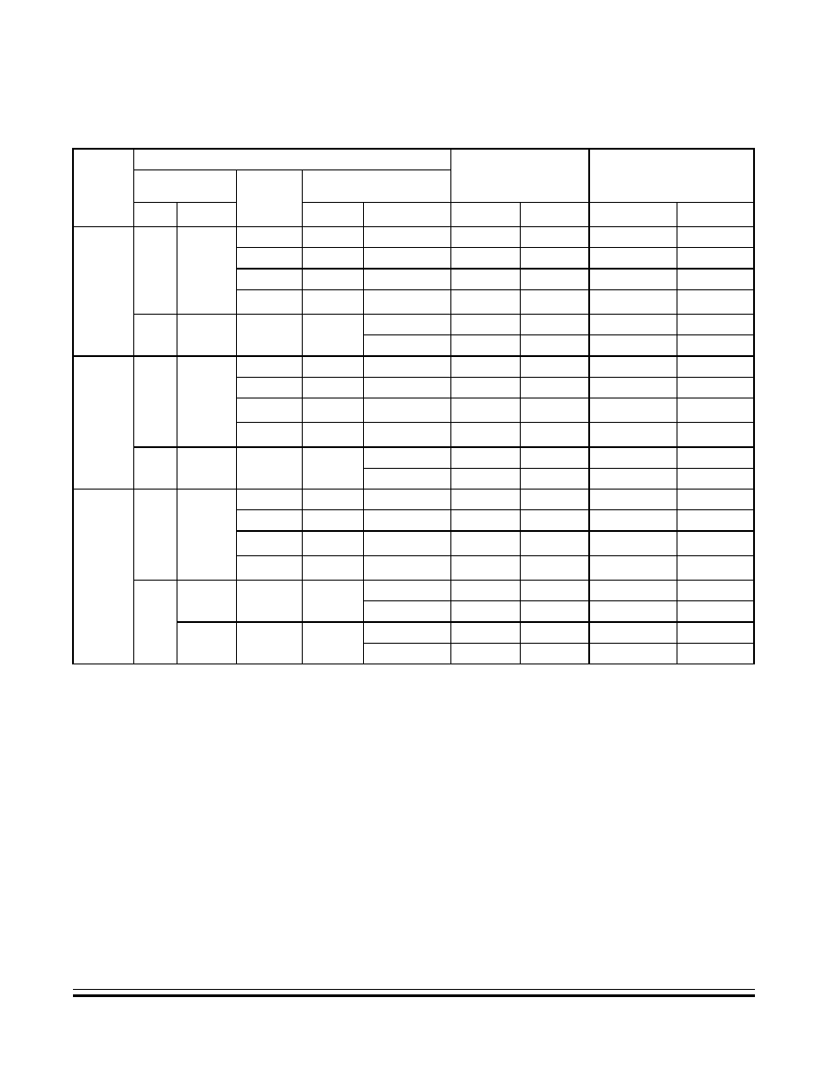
Parallel Input/Output
Port C (28-Pin Versions Only)
MC68HC705JJ7 ∑ MC68HC705JP7 -- REV 4
Advance Information
MOTOROLA
Parallel Input/Output
101
7.5 Port C (28-Pin Versions Only)
Port C is an 8-bit, general-purpose, bidirectional I/O port with these
features:
∑
Individual programmable pulldown devices
∑
High current sinking capability on all port C pins, with a maximum
total for port C
∑
High current sourcing capability on all port C pins, with a maximum
total for port C
Table 7-3. Port B Pin Functions -- PB5≠PB7
Port B
Pin
Control Bits
PORTB Access
(Pin or Data
Register)
Result on
Port B Pins
SIOP
SWPDI
in MOR
Port B
SPE
MSTR
PDIBx
DDRBx
(1)
Read
Write
Pulldown
Pin
PB5
0
X
(2)
0
0
0
Pin
Data
On
PB5 in
0
1
0
Pin
Data
Off
PB5 in
1
X
0
Pin
Data
Off
PB5 in
X
(2)
X
(2)
1
Data
Data
Off
PB5 out
1
X
(2)
X
(2)
X
(2)
0
SDO
Data
Off
SDO out
1
Data
Data
Off
SDO out
PB6
0
X
(2)
0
0
0
Pin
Data
On
PB6 in
0
1
0
Pin
Data
Off
PB6 in
1
X
(2)
0
Pin
Data
Off
PB6 in
X
(2)
X
(2)
1
Data
Data
Off
PB6 out
1
X
(2)
X
(2))
X
(2)
0
SDI
Data
Off
SDI in
1
Data
Data
Off
SDI in
PB7
0
X
(2)
0
0
0
Pin
Data
On
PB7 in
0
1
0
Pin
Data
Off
PB7 in
1
X
(2)
0
Pin
Data
Off
PB7 in
X
(2)
X
(2)
1
Data
Data
Off
PB7 out
1
0
X
(2)
X
(2)
0
SCK
Data
Off
SCK in
1
Data
Data
Off
SCK in
1
X
(2)
X
(2)
0
SCK
Data
Off
SCK out
1
Data
Data
Off
SCK out
1. DDRB can always be read or written.
2. Don't care
Advance Information
MC68HC705JJ7 ∑ MC68HC705JP7 -- REV 4
102
Parallel Input/Output
MOTOROLA
Parallel Input/Output
7.5.1 Port C Data Register
The port C data register (PORTC) contains a bit for each of the port C
pins. When a port C pin is programmed to be an output, the state of its
data register bit determines the state of the output pin. When a port C pin
is programmed to be an input, reading the port C data register returns
the logic state of the pin.
PC7≠PC0 -- Port C Data Bits
These read/write bits are software programmable. Data direction of
each bit is under the control of the corresponding bit in the port C data
direction register (DDRC). Reset has no effect on port C data.
7.5.2 Data Direction Register C
The contents of the port C data direction register (DDRC) determine
whether each port C pin is an input or an output. Writing a logic 1 to a
DDRC bit enables the output buffer for the associated port C pin. A
DDRC bit set to a logic 1 also disables the pulldown device for that pin.
Writing a logic 0 to a DDRC bit disables the output buffer for the
associated port C pin. A reset initializes all DDRC bits to logic 0s,
configuring all port C pins as inputs.
Address:
$0002
Bit 7
6
5
4
3
2
1
Bit 0
Read:
PC7
PC6
PC5
PC4
PC3
PC2
PC1
PC0
Write:
Reset:
Unaffected by reset
Figure 7-13. Port C Data Register (PORTC)

Parallel Input/Output
Port C (28-Pin Versions Only)
MC68HC705JJ7 ∑ MC68HC705JP7 -- REV 4
Advance Information
MOTOROLA
Parallel Input/Output
103
DDRC7≠DDRC0 -- Port C Data Direction Bits
These read/write bits control port C data direction. Reset clears the
DDRC7≠DDRC0 bits.
1 = Corresponding port C pin configured as output and pulldown
device disabled
0 = Corresponding port C pin configured as input
7.5.3 Port C Pulldown Devices
All port C pins can have software programmable pulldown devices
enabled or disabled globally by the SWPDI bit in the MOR. These
pulldown devices are individually controlled by the write-only pulldown
register A (PDRA) shown in
Figure 7-3
. PDICH controls the upper four
pins (PC7≠PC4) and PDICL controls the lower four pins (PC3≠PC0).
Clearing the PDICH or PDICL bits in the PDRA turns on the pulldown
devices if the port C pin is an input. Reading the PDRA returns undefined
results since it is a write-only register. Reset clears the PDICH and
PDICL bits, which turns on all the port C pulldown devices.
7.5.4 Port C Logic
Figure 7-15
shows the I/O logic of port C.
When a port C pin is programmed as an output, reading the port bit
actually reads the value of the data latch and not the voltage on the pin
itself. When a port C pin is programmed as an input, reading the port bit
reads the voltage level on the pin. The data latch can always be written,
regardless of the state of its DDR bit.
Table 7-4
summarizes the
operations of the port C pins.
Address:
$0006
Bit 7
6
5
4
3
2
1
Bit 0
Read:
DDRC7
DDRC6
DDRC5
DDRC4
DDRC3
DDRC2
DDRC1
DDRC0
Write:
Reset:
0
0
0
0
0
0
0
0
Figure 7-14. Data Direction Register C (DDRC)
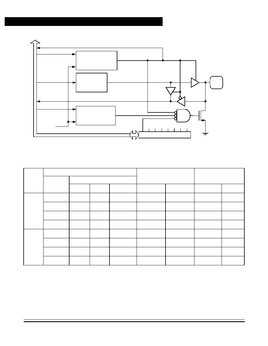
Advance Information
MC68HC705JJ7 ∑ MC68HC705JP7 -- REV 4
104
Parallel Input/Output
MOTOROLA
Parallel Input/Output
Figure 7-15. Port C I/O Circuit
PCx
PORT C DATA
REGISTER
BIT PCx
READ $0006
WRITE $0002
READ $0002
WRITE $0010
PULLDOWN
DEVICE
RESET
IN
TER
N
A
L
D
A
T
A
BU
S
WRITE $0006
DATA DIRECTION
REGISTER C
BIT DDRCx
PULLDOWN
REGISTER A
BIT PDICx
R
R
SW
PD
I
MASK OPTION REGISTER ($1FF1)
HIGH SINK/SOURCE
CURRENT CAPABILITY
Table 7-4. Port C Pin Functions (28-Pin Versions Only)
Port C
Pin(s)
Control Bits
PORTC Access
(Pin or Data Register)
Result on
Port C Pins
SWPDI
in MOR
Port C
PDICH
PDICL
DDRCx
(1)
Read
Write
Pulldown
Pin
PC0
PC1
PC2
PC3
0
X
(2)
0
0
Pin
Data
On
PCx in
0
X
(2)
1
0
Pin
Data
Off
PCx in
1
X
X
(2)
0
Pin
Data
Off
PCx in
X
(2)
X
(2)
X
(2)
1
Data
Data
Off
PCx out
PC4
PC5
PC6
PC7
0
0
X
(2)
0
Pin
Data
On
PCx in
0
1
X
(2)
0
Pin
Data
Off
PCx in
1
X
X
(2)
0
Pin
Data
Off
PCx in
X
(2)
X
(2)
X
(2)
1
Data
Data
Off
PCx out
1. DDRC can always be read or written.
2. Don't care

Parallel Input/Output
Port Transitions
MC68HC705JJ7 ∑ MC68HC705JP7 -- REV 4
Advance Information
MOTOROLA
Parallel Input/Output
105
7.6 Port Transitions
Glitches and temporary floating inputs can occur if the control bits
regarding each port I/O pin are not performed in the correct sequence.
∑
Do not use read-modify-write instructions on pulldown register A
or B.
∑
Avoid glitches on port pins by writing to the port data register
before changing data direction register bits from a logic 0 to a
logic 1.
∑
Avoid a floating port input by clearing its pulldown register bit
before changing its data direction register bit from a logic 1 to a
logic 0.
∑
The SWPDI bit in the MOR turns off all port pulldown devices and
disables software control of the pulldown devices. Reset has no
effect on the pulldown devices when the SWPDI bit is set.
∑
Two or more output pins of the same port can be connected
electrically to provide output currents up to the sum of the
maximum specified drive currents as defined in
15.8 DC
Electrical Characteristics (5.0 Vdc)
and
15.9 DC Electrical
Characteristics (3.0 Vdc)
. Care must be taken to ensure that all
ganged pins always maintain the same output logic value.

Advance Information
MC68HC705JJ7 ∑ MC68HC705JP7 -- REV 4
106
Parallel Input/Output
MOTOROLA
Parallel Input/Output

MC68HC705JJ7 ∑ MC68HC705JP7 -- REV 4
Advance Information
MOTOROLA
Analog Subsystem
107
Advance Information -- MC68HC705JJ7/MC68HC705JP7
Section 8. Analog Subsystem
8.1 Contents
8.2
Introduction . . . . . . . . . . . . . . . . . . . . . . . . . . . . . . . . . . . . . . . 108
8.3
Analog Multiplex Register . . . . . . . . . . . . . . . . . . . . . . . . . . . . 110
8.4
Analog Control Register . . . . . . . . . . . . . . . . . . . . . . . . . . . . . 115
8.5
Analog Status Register . . . . . . . . . . . . . . . . . . . . . . . . . . . . . . 119
8.6
A/D Conversion Methods . . . . . . . . . . . . . . . . . . . . . . . . . . . . 122
8.7
Voltage Measurement Methods . . . . . . . . . . . . . . . . . . . . . . . 132
8.7.1
Absolute Voltage Readings . . . . . . . . . . . . . . . . . . . . . . . . 133
8.7.1.1
Internal Absolute Reference . . . . . . . . . . . . . . . . . . . . . 133
8.7.1.2
External Absolute Reference . . . . . . . . . . . . . . . . . . . . . 134
8.7.2
Ratiometric Voltage Readings . . . . . . . . . . . . . . . . . . . . . . 134
8.7.2.1
Internal Ratiometric Reference . . . . . . . . . . . . . . . . . . .135
8.7.2.2
External Ratiometric Reference . . . . . . . . . . . . . . . . . . . 136
8.8
Voltage Comparator Features . . . . . . . . . . . . . . . . . . . . . . . . 136
8.8.1
Voltage Comparator 1 . . . . . . . . . . . . . . . . . . . . . . . . . . . . 136
8.8.2
Voltage Comparator 2 . . . . . . . . . . . . . . . . . . . . . . . . . . . . 137
8.9
Current Source Features . . . . . . . . . . . . . . . . . . . . . . . . . . . . 138
8.10
Internal Temperature Sensing Diode Features. . . . . . . . . . . . 138
8.11
Sample and Hold . . . . . . . . . . . . . . . . . . . . . . . . . . . . . . . . . . 138
8.12
Port B Interaction with Analog Inputs . . . . . . . . . . . . . . . . . . .139
8.13
Port B Pins as Inputs . . . . . . . . . . . . . . . . . . . . . . . . . . . . . . . 139
8.14
Port B Pulldowns . . . . . . . . . . . . . . . . . . . . . . . . . . . . . . . . . . 139
8.15
Noise Sensitivity . . . . . . . . . . . . . . . . . . . . . . . . . . . . . . . . . . . 140

Advance Information
MC68HC705JJ7 ∑ MC68HC705JP7 -- REV 4
108
Analog Subsystem
MOTOROLA
Analog Subsystem
8.2 Introduction
The analog subsystem of the MC68HC705JJ7/MC68HC705JP7 is
based on two on-chip voltage comparators and a selectable current
charge/discharge function as shown in
Figure 8-1
.
This configuration provides several features:
∑
Two independent voltage comparators with external access to
both inverting and non-inverting inputs
∑
One voltage comparator can be connected as a single-slope
analog-to-digital (A/D) and the other connected as a
single-voltage comparator. The possible single-slope A/D
connection provides these features:
≠
A/D conversions can use V
DD
or an external voltage as a
reference with software used to calculate ratiometric or
absolute results
≠
Channel access of up to four inputs via multiplexer control with
independent multiplexer control allowing mixed input
connections
≠
Access to V
DD
and V
SS
for calibration
≠
Divide by 2 to extend input voltage range
≠
Each comparator can be inverted to calculate input offsets.
≠
Internal sample and hold capacitor
≠
Direct digital output of comparator 1 to the PB4 pin
Voltages are resolved by measuring the time it takes an external
capacitor to charge up to the level of the unknown input voltage being
measured. The beginning of the A/D conversion time can be started by
several means:
∑
Output compare from the 16-bit programmable timer
∑
Timer overflow from the 16-bit programmable timer
∑
Direct software control via a register bit
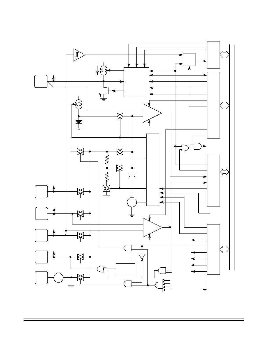
Analog Subsystem
Introduction
MC68HC705JJ7 ∑ MC68HC705JP7 -- REV 4
Advance Information
MOTOROLA
Analog Subsystem
109
Figure 8-1. Analog Subsystem Block Diagram
ANALOG
INTERRUPT
PB0
V
DD
TO
F
OC
F
AN0
CHARGE
CURRENT
CHG
≠
+
PB1
AN1
V
DD
PB2
AN2
PB3
AN3
PB4
AN4
INV
COMP2
PORTB
LOGIC
MUX4
MUX3
MUX1
MUX2
SAMPLE
PORTB
LOGIC
PORTB
LOGIC
PORTB
LOGIC
PORTB
LOGIC
I
CHG
HOLD
INV
DHOLD
V
REF
MUX4
MUX3
MUX2
MUX1
I
DISCHG
2 TO 1
MUX
16-
BIT
PR
OG
.
AN
AL
OG
TCAP
I
N
T
E
RN
AL
HC
05
BU
S
CMP2
CMP1
CAP
TCAP
TCMP
MUX4
MUX3
MUX2
C
H
A
NNE
L SEL
EC
T
B
U
S
CP1EN
MUX1
V
REF
ISEN
CP2EN
AN
A
L
O
G
CO
NTR
O
L
RE
GI
STE
R
(AC
R
)
ICEN
CPIE
CP1EN
CP2EN
MU
X R
E
G
I
ST
ER
(A
MU
X)
CPF1
AN
AL
OG
ST
ATU
S
REG
I
S
T
ER
(AS
R
)
CPF2
PB3/AN3/TCAP
TI
M
E
R
≠
+
INV
COMP1
ATD2
ATD1
ICF
CONTROL
LOGIC
V
DD
TEMPERATURE
DIODE
INTERNAL
V
REF
V
SS
DENOTES
INTERNAL
ANALOG V
SS
V
SS
+
≠
V
AOFF
$001D
$001E
$0003
VOFF
OPT (COPR)
100 MV
OFFSET
+
≠
CO
MP
AR
AT
OR
IN
PU
T S
E
L
E
CT
AN
D
S
A
M
P
LE
C
O
NT
RO
L
PORT B
CONTROL
COE1
OPT (COPR)
LOGIC
OLVL
80 k
80 k
AV
SS
= V
SS
= V
AOFF

Advance Information
MC68HC705JJ7 ∑ MC68HC705JP7 -- REV 4
110
Analog Subsystem
MOTOROLA
Analog Subsystem
The end of the A/D conversion time can be captured by these means:
∑
Input capture in the 16-bit programmable timer
∑
Interrupt generated by the comparator output
∑
Software polling of the comparator output using software loop time
8.3 Analog Multiplex Register
The analog multiplex register (AMUX) controls the general
interconnection and operation. The control bits in the AMUX are shown
in
Figure 8-2
.
HOLD, DHOLD
These read/write bits control the source connection to the negative
input of voltage comparator 2 shown in
Figure 8-3
. This allows the
voltage on the internal temperature sensing diode, the channel
selection bus, or the divide-by-two channel selection bus to charge
the internal sample capacitor and to also be presented to comparator
2. The decoding of these sources is given in
Table 8-1
.
During the hold case when both the HOLD and DHOLD bits are clear,
the VOFF bit in the analog status register (ASR) can offset the V
SS
reference on the sample capacitor by approximately 100 mV. This
offset source is bypassed whenever the sample capacitor is being
charged with either the HOLD or DHOLD bit set. The VOFF bit must
be enabled by the OPT bit in the COPR at location $1FF0.
Address:
$0003
Bit 7
6
5
4
3
2
1
Bit 0
Read:
HOLD
DHOLD
INV
VREF
MUX4
MUX3
MUX2
MUX1
Write:
Reset:
1
0
0
0
0
0
0
0
Figure 8-2. Analog Multiplex Register (AMUX)
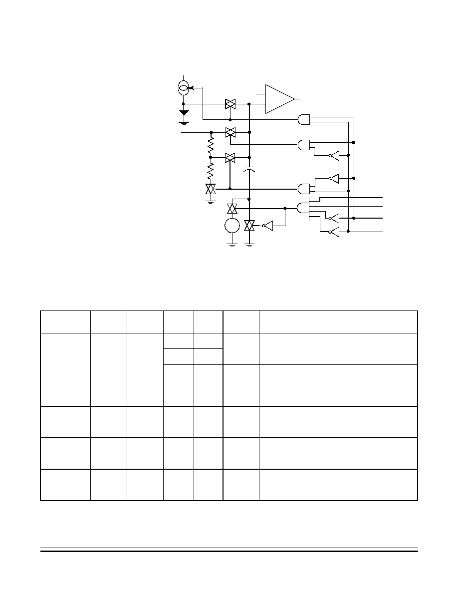
Analog Subsystem
Analog Multiplex Register
MC68HC705JJ7 ∑ MC68HC705JP7 -- REV 4
Advance Information
MOTOROLA
Analog Subsystem
111
Figure 8-3. Comparator 2 Input Circuit
≠
+
COMP2
SAMPLE
HOLD
DHOLD
CAP
TEMPERATURE
DIODE
INTERNAL
VOFF
V
SS
OFFSET
+
≠
OPT (MOR)
CHANNEL
PB0
SELECTION
BUS
V
DD
80 k
80 k
Table 8-1. Comparator 2 Input Sources
Case
HOLD
(AMUX)
DHOLD
(AMUX)
OPT
(MOR)
VOFF
(ASR)
Voltage
Offset
Source To Negative Input
of Comparator 2
Hold
sample
voltage
0
0
0
X
(1)
No
Sample capacitor connected to
comparator 2 negative input; very low leakage
current.
1
0
1
1
Yes
Sample capacitor connected to comparator 2
negative input; bottom of capacitor offset from
V
SS
by approximately 100 mV, very low
leakage current.
Divide input
0
1
X
(1)
X
(1)
No
Signal on channel selection bus is divided
by 2 and connected to sample capacitor
and comparator 2 negative input
Direct input
1
0
X
(1)
X
(1)
No
Signal on channel selection bus is connected
directly to sample capacitor and comparator 2
negative input.
Internal
temperature
diode
1
1
X
(1)
X
(1)
No
Internal temperature sensing diode connected
directly to sample capacitor and comparator 2
negative input.
1. Don't care

Advance Information
MC68HC705JJ7 ∑ MC68HC705JP7 -- REV 4
112
Analog Subsystem
MOTOROLA
Analog Subsystem
During a reset, the HOLD bit is set and the DHOLD bit is cleared,
which connects the internal sample capacitor to the channel selection
bus. And since a reset also clears the MUX[1:4] bits, then the channel
selection bus will be connected to V
SS
and the internal sample
capacitor will be discharged to V
SS
following the reset.
NOTE:
When sampling a voltage for later conversion, the HOLD and DHOLD
bits should be cleared before making any changes in the MUX channel
selection. If the MUX channel and the HOLD/DHOLD are changed on
the same write cycle to the AMUX register, the sampled voltage may be
altered during the channel switching.
INV
This is a read/write bit that controls the relative polarity of the inherent
input offset voltage of the voltage comparators. This bit allows voltage
comparisons to be made with both polarities and then averaged
together by taking the sum of the two readings and then dividing by 2
(logical shift right).
The polarity of the input offset is reversed by interchanging the
internal voltage comparator inputs while also inverting the comparator
output. This interchange does not alter the action of the voltage
comparator output with respect to its port pins. That is, the output will
only go high if the voltage on the positive input (PB2 pin for
comparator 1 and PB0 pin for comparator 2) is above the voltage on
the respective negative input (PB3 pin for comparator 1 and PB1 pin
for comparator 2). This is shown schematically in
Figure 8-4
. This bit
is cleared by a reset of the device.
1 = The voltage comparators are internally inverted.
0 = The voltage comparators are not internally inverted.
NOTE:
The effect of changing the state of the INV bit is to only change the
polarity of the input offset voltage. It does not change the output phase
of the CPF1 or CPF2 flags with respect to the external port pins.
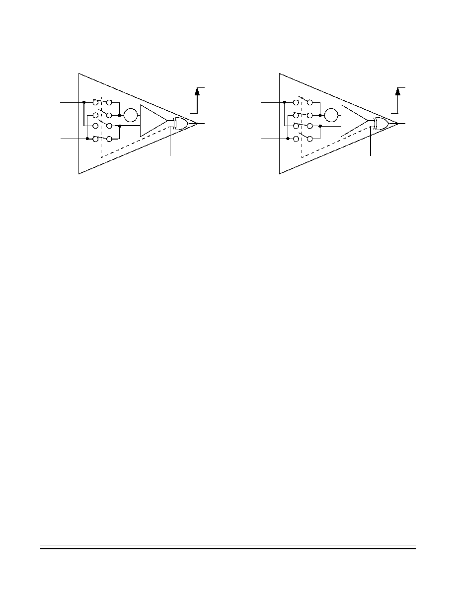
Analog Subsystem
Analog Multiplex Register
MC68HC705JJ7 ∑ MC68HC705JP7 -- REV 4
Advance Information
MOTOROLA
Analog Subsystem
113
Figure 8-4. INV Bit Action
NOTE:
Either comparator may generate an output flag when the inputs are
exchanged due to a change in the state of the INV bit. It is therefore
recommended that the INV bit not be changed while waiting for a
comparator flag. Further, any changes to the state of the INV bit should
be followed by writing a logic 1 to both the CPFR1 and CPFR2 bits to
clear any extraneous CPF1 or CPF2 flags that may have occurred.
VREF
This read/write bit connects the channel select bus to V
DD
for making
a reference voltage measurement. It cannot be selected if any of the
other input sources to the channel select bus are selected as shown
in
Table 8-2
. This bit is cleared by a reset of the device.
1 = Channel select bus connected to V
DD
if all MUX1:4 are cleared.
0 = Channel select bus cannot be connected to V
DD
.
MUX1:4
These are read/write bits that connect the analog subsystem pins to
the channel select bus and voltage comparator 2 for purposes of
making a voltage measurement. They can be selected individually or
combined with any of the other input sources to the channel select
bus as shown in
Table 8-2
.
NOTE:
The V
AOFF
voltage source shown in
Figure 8-1
depicts a small offset
voltage generated by the total chip current passing through the package
bond wires and lead frame that are attached to the single V
SS
pin. This
offset raises the internal V
SS
reference (AV
SS
) in the analog subsystem
V≠
V+
INV = 0
+
COMP
V
IO
≠
RISE
WHEN
V+ > V≠
INV = 1
V+
V≠
+
COMP
V
IO
≠
RISE
WHEN
V+ > V≠

Advance Information
MC68HC705JJ7 ∑ MC68HC705JP7 -- REV 4
114
Analog Subsystem
MOTOROLA
Analog Subsystem
with respect to the external V
SS
pin. Turning on the V
SS
MUX to the
channel select bus connects it to this internal AV
SS
reference line.
When making A/D conversions, this AV
SS
offset gets placed on the
external ramping capacitor since the discharge device on the PB0/AN0
pin discharges the external capacitor to the internal AV
SS
line. Under
these circumstances, the positive input (+) to comparator 2 will always
be higher than the negative input (≠) until the negative input reaches the
AV
SS
offset voltage plus any offset in comparator 2.
Therefore, input voltages cannot be resolved if they are less than the
sum of the AV
SS
offset and the comparator offset, because they will
always yield a low output from the comparator.
Table 8-2. Channel Select Bus Combinations
Analog Multiplex Register
Channel Select Bus Connected to:
VREF
MUX4
MUX3
MUX2
MUX1
V
DD
PB4/AN4/
TCMP
PB3/AN3/
TCAP
PB2/AN2
PB1/AN1
V
SS
0
0
0
0
0
Hi-Z
Hi-Z
Hi-Z
Hi-Z
Hi-Z
On
X
(1)
0
0
0
1
Hi-Z
Hi-Z
Hi-Z
Hi-Z
On
Hi-Z
X
(1)
0
0
1
0
Hi-Z
Hi-Z
Hi-Z
On
Hi-Z
Hi-Z
X
(1)
0
0
1
1
Hi-Z
Hi-Z
Hi-Z
On
On
Hi-Z
X
(1)
0
1
0
0
Hi-Z
Hi-Z
On
Hi-Z
Hi-Z
Hi-Z
X
(1)
0
1
0
1
Hi-Z
Hi-Z
On
Hi-Z
On
Hi-Z
X
(1)
0
1
1
0
Hi-Z
Hi-Z
On
On
Hi-Z
Hi-Z
X
(1)
0
1
1
1
Hi-Z
Hi-Z
On
On
On
Hi-Z
X
(1)
1
0
0
0
Hi-Z
On
Hi-Z
Hi-Z
Hi-Z
Hi-Z
X
(1)
1
0
0
1
Hi-Z
On
Hi-Z
Hi-Z
On
Hi-Z
X
(1)
1
0
1
0
Hi-Z
On
Hi-Z
On
Hi-Z
Hi-Z
X
(1)
1
0
1
1
Hi-Z
On
Hi-Z
On
On
Hi-Z
X
(1)
1
1
0
0
Hi-Z
On
On
Hi-Z
Hi-Z
Hi-Z
X
(1)
1
1
0
1
Hi-Z
On
On
Hi-Z
On
Hi-Z
X
(1)
1
1
1
0
Hi-Z
On
On
On
Hi-Z
Hi-Z
X
(1)
1
1
1
1
Hi Z
On
On
On
On
Hi Z
1. Don/t care

Analog Subsystem
Analog Control Register
MC68HC705JJ7 ∑ MC68HC705JP7 -- REV 4
Advance Information
MOTOROLA
Analog Subsystem
115
8.4 Analog Control Register
The analog control register (ACR) controls the power-up, interrupt, and
flag operation. The analog subsystem draws current while it is operating.
The resulting power consumption can be reduced by powering down the
analog subsystem when not in use (refer to
15.6 Supply Current
Characteristics (V
DD
= 4.5 to 5.5 Vdc)
). This can be done by clearing
three enable bits (ISEN, CP1EN, and CP2EN) in the ACR at $001D.
Since these bits are cleared following a reset, the voltage comparators
and the charge current source will be powered down following a reset of
the device.
The control bits in the ACR are shown in
Figure 8-5
. All the bits in this
register are cleared by a reset of the device.
CHG
The CHG enable bit allows direct control of the charge current source
and the discharge device and also reflects the state of the discharge
device. This bit is cleared by a reset of the device.
1 = If the ISEN bit is also set, the charge current source is sourcing
current out of the PB0/AN0 pin. Writing a logic 1 enables the
charging current out of the PB0/AN0 pin.
0 = The discharge device is sinking current into the PB0/AN0 pin.
Writing a logic 0 disables the charging current and enables the
discharging current into the PB0/AN0 pin, if the ISEN bit is also
set.
Address:
$001D
Bit 7
6
5
4
3
2
1
Bit 0
Read:
CHG
ATD2
ATD1
ICEN
CPIE
CP2EN
CP1EN
ISEN
Write:
Reset:
0
0
0
0
0
0
0
0
Figure 8-5. Analog Control Register (ACR)

Advance Information
MC68HC705JJ7 ∑ MC68HC705JP7 -- REV 4
116
Analog Subsystem
MOTOROLA
Analog Subsystem
ATD1≠ATD2
The ATD1≠ATD2 enable bits select one of the four operating modes
used for making A/D conversions via the single-slope method.These
four modes are given in
Table 8-3
. These bits have no effect if the
ISEN enable bit is cleared. These bits are cleared by a reset of the
device and thereby return the analog subsystem to the manual A/D
conversion method.
ICEN
This is a read/write bit that enables a voltage comparison to trigger the
input capture register of the programmable timer when the CPF2 flag
bit is set. Therefore, an A/D conversion could be started by receiving
an OCF or TOF from the programmable timer and then terminated
when the voltage on the external ramping capacitor reaches the level
of the unknown voltage. The time of termination will be stored in the
Table 8-3. A/D Conversion Options
A/D
Option
Mode
Charge
Control
A/D Options
Current Flow
to/from PB0/AN0
ISEN
ATD2
ATD1
CHG
Disabled
Current
source and
discharge
disabled
0
X
X
X
Current control disabled,
no source or sink current
1
0
0
1
Begin sourcing current
when the CHG bit is set
and continue to source
current until the CHG bit
is cleared.
1
1
0
1
The CHG bit remains set
until the next time ICF
occurs.
3
Automatic
charge and
discharge
(OCF≠ICF)
synchronized
to timer
1
1
1
0
The CHG bit remains
cleared until the next
time OCF occurs.
1
1
1
1
The CHG bit remains set
until the next time ICF
occurs.

Analog Subsystem
Analog Control Register
MC68HC705JJ7 ∑ MC68HC705JP7 -- REV 4
Advance Information
MOTOROLA
Analog Subsystem
117
16-bit buffer located at $0014 and $0015. This bit is automatically set
whenever mode 2 or 3 is selected by setting the ATD2 control bit. This
bit is cleared by a reset of the device.
1 = Connects the CPF2 flag bit to the timer input capture register
0 = Connects the PB3/AN3 pin to the timer input capture register
NOTE:
For the input capture to occur when the output of comparator 2 goes
high, the IEDG bit in the TCR must also be set.
When the ICEN bit is set, the input capture function of the programmable
timer is not connected to the PB3/AN3/TCAP pin but is driven by the
CPF2 output flag from comparator 2. To return to capturing times from
external events, the ICEN bit must first be cleared before the timed event
occurs.
CPIE
This is a read/write bit that enables an analog interrupt when either of
the CPF1 or CPF2 flag bits is set to a logic 1. This bit is cleared by a
reset of the device.
1 = Enables analog interrupts when comparator flag bits are set
0 = Disables analog interrupts when comparator flag bits are set
NOTE:
If both the ICEN and CPIE bits are set, they will both generate an
interrupt by different paths. One will be the programmable timer interrupt
due to the input capture and the other will be the analog interrupt due to
the output of comparator 2 going high. In this case, the input capture
interrupt will be entered first due to its higher priority. The analog
interrupt will then need to be serviced even if the comparator 2 output
has been reset or the input capture flag (ICF) has been cleared.
CP2EN
The CP2EN enable bit controls power to voltage comparator 2 in the
analog subsystem. Powering down a comparator will drop the supply
current. This bit is cleared by a reset of the device.
1 = Writing a logic 1 powers up voltage comparator 2.
0 = Writing a logic 0 powers down voltage comparator 2.

Advance Information
MC68HC705JJ7 ∑ MC68HC705JP7 -- REV 4
118
Analog Subsystem
MOTOROLA
Analog Subsystem
NOTE:
Voltage comparators power up slower than digital logic and their outputs
may go through indeterminate states which might set their respective
flags (CPF1, CPF2). It is therefore recommended to power up the
charge current source first (ISEN), then to power up any comparators,
and finally clear the flag bits by writing a logic 1 to the respective CPFR1
or CPFR2 bits in the ACR.
CP1EN
The CP1EN enable bit will power down the voltage comparator 1 in
the analog subsystem. Powering down a comparator will drop the
supply current. This bit is cleared by a reset of the device.
1 = Writing a logic 1 powers up voltage comparator 1
0 = Writing a logic 0 powers down voltage comparator 1
ISEN
The ISEN enable bit will power down the charge current source and
disable the discharge device in the analog subsystem. Powering
down the current source will drop the supply current by about 200
µ
A.
This bit is cleared by a reset of the device.
1 = Writing a logic 1 powers up the ramping current source and
enables the discharge device on the PB0/AN0 pin.
0 = Writing a logic 0 powers down the ramping current source and
disables the discharge device on the PB0/AN0 pin.
NOTE:
The analog subsystem has support circuitry which draws current. This
current will be powered down if both comparators and the charge current
source are powered down (ISEN, CP1EN, and CP2EN all cleared).
Powering up either comparator or the charge current source will activate
the support circuitry.
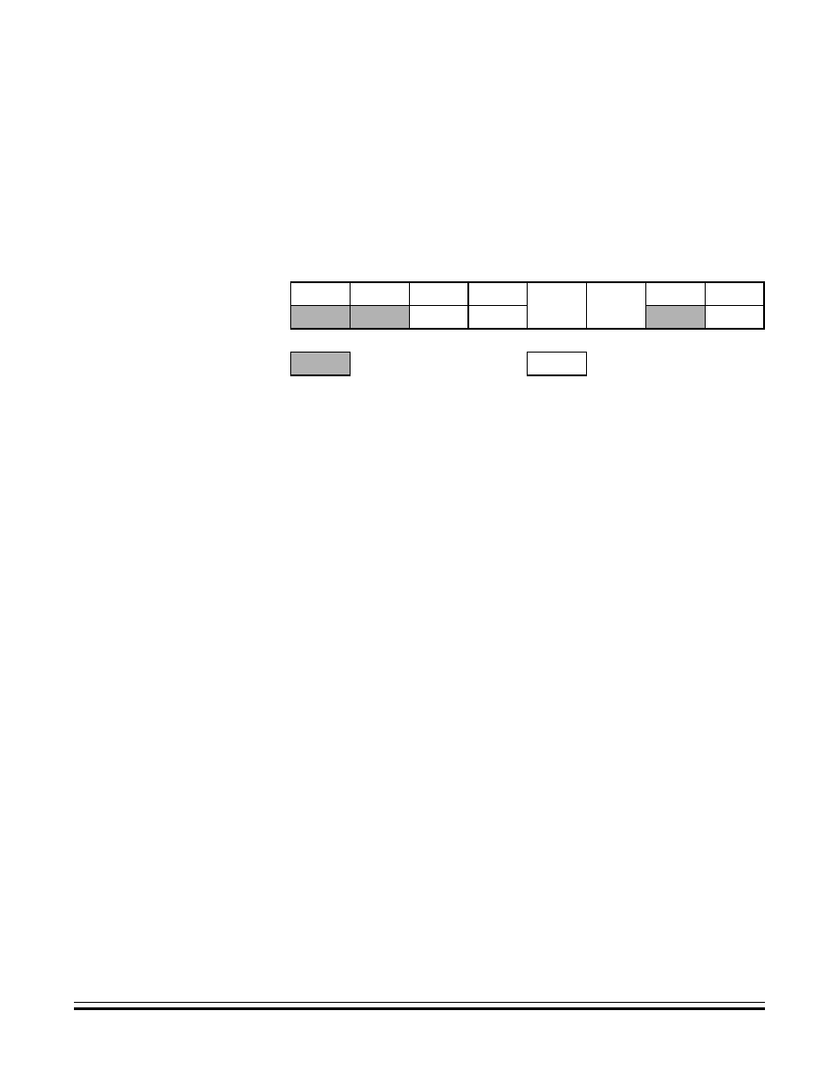
Analog Subsystem
Analog Status Register
MC68HC705JJ7 ∑ MC68HC705JP7 -- REV 4
Advance Information
MOTOROLA
Analog Subsystem
119
8.5 Analog Status Register
The analog status register (ASR) contains status and control of the
comparator flag bits. These bits in the ASR are shown in
Figure 8-6
. All
the bits in this register are cleared by a reset of the device.
CPF2
This read-only flag bit is edge sensitive to the rising output of
comparator 2. It is set when the voltage on the PB0/AN0 pin rises
above the voltage on a sample capacitor which creates a positive
edge on the output of comparator 2, regardless of the state of the INV
bit in the AMUX register. This bit is reset by writing a logic 1 to the
CPFR2 reset bit in the ASR. This bit is cleared by a reset of the
device.
1 = A positive transition on the output of comparator 2 has occurred
since the last time the CPF2 flag has been cleared.
0 = A positive transition on the output of comparator 2 has not
occurred since the last time the CPF2 flag has been cleared.
CPF1
This read-only flag bit is edge sensitive to the rising output of
comparator 1. It is set when the voltage on the PB2/AN2 pin rises
above the voltage on the PN3/AN3/TCAP pin which creates a positive
edge on the output of comparator 1, regardless of the state of the INV
bit in the AMUX register. This bit is reset by writing a logic 1 to the
CPFR1 reset bit in the ASR. This bit is cleared by a reset of the
device.
1 = A positive transition on the output of comparator 1 has occurred
since the last time the CPF1 flag has been cleared.
0 = A positive transition on the output of comparator 1 has not
occurred since the last time the CPF1 flag has been cleared.
Address:
$001E
Bit 7
6
5
4
3
2
1
Bit 0
Read:
CPF2
CPF1
0
0
COE1
VOFF
CMP2
CMP1
Write:
CPFR2
CPFR1
R
Reset:
0
0
0
0
0
0
0
0
= Unimplemented
R
= Reserved
Figure 8-6. Analog Status Register (ASR)

Advance Information
MC68HC705JJ7 ∑ MC68HC705JP7 -- REV 4
120
Analog Subsystem
MOTOROLA
Analog Subsystem
CPFR2
Writing a logic 1 to this write-only flag clears the CPF2 flag in the ASR.
Writing a logic 0 to this bit has no effect. Reading the CPFR2 bit will
return a logic 0. By default, this bit looks cleared following a reset of
the device.
1 = Clears the CPF2 flag bit
0 = No effect
CPFR1
Writing a logic 1 to this write-only flag clears the CPF1 flag in the ASR.
Writing a logic 0 to this bit has no effect. Reading the CPFR1 bit will
return a logic 0. By default, this bit looks cleared after a reset of the
device.
1 = Clears the CPF1 flag bit
0 = No effect
NOTE:
The CPFR1 and CPFR2 bits should be written with logic 1s following a
power-up of either comparator. This will clear out any latched CPF1 or
CPF2 flag bits which might have been set during the slower power-up
sequence of the analog circuitry.
If both inputs to a comparator are above the maximum common-mode
input voltage (V
DD
≠1.5 V), the output of the comparator is indeterminate
and may set the comparator flag. Applying a reset to the device may only
temporarily clear this flag as long as both inputs of a comparator remain
above the maximum common-mode input voltages.
VOFF
This read-write bit controls the addition of an offset voltage to the
bottom of the sample capacitor. It is not active unless the OPT bit in
the COPR at location $1FF0 is set. Any reads of the VOFF bit location
return a logic 0 if the OPT bit is clear. During the time that the sample
capacitor is connected to an input (either HOLD or DHOLD set), the
bottom of the sample capacitor is connected to V
SS
. The VOFF bit is
cleared by a reset of the device. For more information, see
8.11
Sample and Hold
.
1 = Enables approximately 100 mV offset to be added to the
sample voltage when both the HOLD and DHOLD control bits
are cleared
0 = Connects the bottom of the sample capacitor to V
SS

Analog Subsystem
Analog Status Register
MC68HC705JJ7 ∑ MC68HC705JP7 -- REV 4
Advance Information
MOTOROLA
Analog Subsystem
121
COE1
This read-write bit controls the output of comparator 1 to the PB4 pin.
It is not active unless the OPT bit in the COPR at location $1FF0 is
set. Any reads of the COE1 bit location return a logic 0 if the OPT bit
is clear. The COE1 bit is cleared by a reset of the device.
1 = Enables the output of comparator 1 to be ORed with the PB4
data bit and OLVL bit, if the DDRB4 bit is also set
0 = Disables the output of comparator 1 from affecting the PB4 pin
CMP2
This read-only bit shows the state of comparator 2 during the time that
the bit is read. This bit is therefore the current state of the comparator
without any latched history. The CMP2 bit will be high if the voltage
on the PB0/AN0 pin is greater than the voltage on the PB1/AN1 pin,
regardless of the state of the INV bit in the AMUX register. Since a
reset disables comparator 2, this bit returns a logic 0 following a reset
of the device.
1 = The voltage on the positive input on comparator 2 is higher than
the voltage on the negative input of comparator 2.
0 = The voltage on the positive input on comparator 2 is lower than
the voltage on the negative input of comparator 2.
CMP1
This read-only bit shows the state of comparator 1 during the time that
the bit is read. This bit is therefore the current state of the comparator
without any latched history. The CMP1 bit will be high if the voltage
on the PB2/AN2 pin is greater than the voltage on the PB3/AN3/TCAP
pin, regardless of the state of the INV bit in the AMUX register. Since
a reset disables comparator 1, this bit returns a logic 0 following a
reset of the device.
1 = The voltage on the positive input on comparator 1 is higher than
the voltage on the negative input of comparator 1.
0 = The voltage on the positive input on comparator 1 is lower than
the voltage on the negative input of comparator 1.
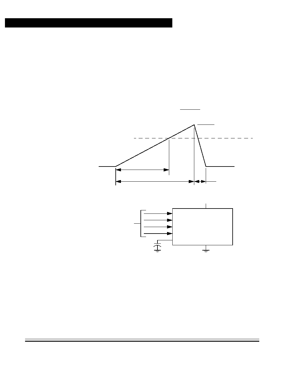
Advance Information
MC68HC705JJ7 ∑ MC68HC705JP7 -- REV 4
122
Analog Subsystem
MOTOROLA
Analog Subsystem
8.6 A/D Conversion Methods
The control bits in the ACR provide various options to charge or
discharge current through the PB0/AN0 pin to perform single-slope A/D
conversions using an external capacitor from the PB0/AN0 pin to V
SS
as
shown in
Figure 8-7
. The various A/D conversion triggering options are
given in
Table 8-3
.
Figure 8-7. Single-Slope A/D Conversion Method
The top three bits of the ACR control the charging and discharging
current into or out of the PB0/AN0 pin. These three bits will have no
effect on the PB0/AN0 pin if the ISEN enable bit is cleared. Any clearing
of the ISEN bit will immediately disable both the charge current source
and the discharge device. Since all these bits and the ISEN bit are
UNKNOWN VOLTAGE ON (≠) INPUT
CHARGE TIME
TO MATCH UNKNOWN
DISCHARGE TIME
TO RESET CAPACITOR
VOLTAGE ON
CAPACITOR
CONNECTED
TO (+) INPUT
MAXIMUM CHARGE TIME
TO V
DD
≠1.5 Vdc
V
DD
≠1.5 Vdc
C x V
X
I
V
DD
+ 5 V
RAMP
CAP
V
SS
PB0/AN0
PB1/AN1
PB2/AN2
PB3/AN3
PB4/AN4
UNKNOWN
OR REFERENCE
MC68HC705JJ7
Charge Time =
MC68HC705JP7
SIGNALS

Analog Subsystem
A/D Conversion Methods
MC68HC705JJ7 ∑ MC68HC705JP7 -- REV 4
Advance Information
MOTOROLA
Analog Subsystem
123
cleared when the device is reset, the MC68HC705JJ7/MC68HC705JP7
starts with the charge and discharge function disabled.
The length of time required to reach the maximum voltage to be
measured and the speed of the time counting mechanism will determine
the resolution of the reading. The time to ramp the external capacitor
voltage to match the maximum voltage is dependent on:
∑
Charging current to external capacitor
∑
Value of the external capacitor
∑
Clock rate for timing function
∑
Any prescaling of the clock to the timing function
∑
Desired resolution
The charging behavior is described by the general equation:
t
CHG
= C
EXT
x V
X
/ I
CHG
Where:
t
CHG
= Charge time (seconds)
C
EXT
= Capacitance (
µ
F)
V
X
= Unknown voltage (volts)
I
CHG
= Charge current (
µ
A)
Since the MCU can measure time in a variety of ways, the resolution of
the conversion will depend on the length of the time keeping function and
its prescaling to the oscillator frequency (f
OSC
). Therefore, the charge
time also equals:
t
CHG
= P x N / f
OSC
Where:
P
= Prescaler value (
˜
2,
˜
4,
˜
8, etc.)
N
= Number of counts during charge time
f
OSC
= Oscillator clock frequency (Hz)

Advance Information
MC68HC705JJ7 ∑ MC68HC705JP7 -- REV 4
124
Analog Subsystem
MOTOROLA
Analog Subsystem
NOTE:
Noise on the system ground or the external ramping capacitor can cause
the comparator to trip prematurely. Therefore, in any given application it
is best to use the fastest possible ramp rate (shortest charge time).
The previous two equations for the charge time, t
CHG
, can be combined
to form the following expression for the full scale count (N
FS
) of the
measured time versus the full scale unknown voltage (V
FS
):
N
FS
= C
EXT
x V
FS
x f
OSC
/ (P x I
CHG
)
Since a given timing method has a fixed charge current and prescaler,
then the variation in the resultant count for a given unknown voltage is
mainly dependent on the operating frequency and the capacitance value
used. The desired external capacitance for a given voltage range, f
OSC
,
conversion method, and resolution is defined as:
C
EXT
= N
FS
x P x I
CHG
/ (V
FS
x f
OSC
)
NOTE:
The value of any capacitor connected directly to the PB0/AN0 pin should
be limited to less than 2 microfarads. Larger capacitances will create
high discharge currents which may damage the device or create signal
noise.
The full scale voltage range for a given capacitance, f
OSC
, conversion
method, and resolution is defined as:
V
FS
= N
FS
x P x I
CHG
/ (C
EXT
x f
OSC
)
Once charged to a given voltage, a finite amount of time will be required
to discharge the capacitor back to its start voltage at V
SS
. This discharge
time will be solely based on the value of capacitance used and the
sinking current of the internal discharge device. To allow a reasonable
time for the capacitor to return to V
SS
levels, the discharge time should
last about 10 milliseconds per microfarad of capacitance attached to the
PB0 pin. If the total charge/discharge cycle time is critical, then the
discharge time should be at least 1/10 of the most recent charge time.
Shorter discharge times may be used if lesser accuracy in the voltage
measurement is acceptable.

Analog Subsystem
A/D Conversion Methods
MC68HC705JJ7 ∑ MC68HC705JP7 -- REV 4
Advance Information
MOTOROLA
Analog Subsystem
125
NOTE:
Sufficient time should be allowed to discharge the external capacitor or
subsequent charge times will be shortened with resultant errors in timing
conversion.
Table 8-4
gives the range of values of each parameter in the A/D timing
conversion and
Table 8-5
gives some A/D conversion examples for
several bit resolutions.
The mode selection bits in the ACR allow four methods of single-slope
A/D conversion. Each of these methods is shown in
Figure 8-8
through
Figure 8-11
using the signal names and parameters given in
Table 8-4
.
∑
Manual start and stop (mode 0)
Figure 8-8
∑
Manual start and automatic discharge (mode 1)
Figure 8-9
∑
Automatic start and stop from TOF to ICF (mode 2)
Figure 8-10
∑
Automatic start and stop from OCF to ICF (mode 3)
Figure 8-11
Advance Information
MC68HC705JJ7 ∑ MC68HC705JP7 -- REV 4
126
Analog Subsystem
MOTOROLA
Analog Subsystem
Table 8-4. A/D Conversion Parameters
Name
Function
Min
Typ
Max
Units
V
X
Unknown voltage on channel selection bus
V
SS
--
V
DD
≠1.5
V
V
MAX
Maximum charging voltage on external capacitor
--
--
V
DD
≠1.5
V
I
CHG
Charging current on external ramping capacitor
V
DD
= 3 Vdc
V
DD
= 5 Vdc
Refer to
15.10 Analog Subsystem
Characteristics (5.0 Vdc)
and
15.11 Analog
Subsystem Characteristics (3.0 Vdc)
I
DIS
Discharge current on external ramping capacitor
Refer to
15.10 Analog Subsystem
Characteristics (5.0 Vdc)
and
15.11 Analog
Subsystem Characteristics (3.0 Vdc)
t
CHG
Time to charge external capacitor
(100 kHz < f
OSC
< 4.0 MHz)
4-bit result
6-bit result
8-bit result
10-bit result
12-bit result
0.032
0.128
0.512
2.048
8.192
0.128
0.512
2.048
8.196
32.768
2.56
10.24
40.96
120
(1)
120
(1)
ms
t
DIS
Time to discharge external capacitor, C
EXT
--
5
10
ms
/ µ
F
C
EXT
Capacitance of external ramping capacitor
0.0001
0.1
2.0
µ
F
N
Number of counts for I
CHG
to charge C
EXT
to V
X
1
1024
65536
Counts
P
Prescaler into timing function (
˜
P)
Using core timer
Using 16-bit programmable timer
Using software loops
8
8
24
8
8
User defined
8
8
User defined
˜
P
f
OSC
Clock source frequency (excluding any prescaling)
Refer to
15.12 Control Timing (5.0 Vdc)
and
15.13 Control Timing (3.0 Vdc)
1. Limited by requirement for C
EXT
to be less than 2.0
µ
F
Analog Subsystem
A/D Conversion Methods
MC68HC705JJ7 ∑ MC68HC705JP7 -- REV 4
Advance Information
MOTOROLA
Analog Subsystem
127
Table 8-5. Sample Conversion Timing (V
DD
= 5.0 Vdc)
Bits
Counts
V
X
(Vdc)
A/D Method
Clock Source
f
OSC
(MHz)
t
CHG
(ms)
C
EXT
(
µ
F)
4
16
3.5
Software loop
(12 bus cycles)
(24 f
OSC
cycles)
Mode 0 or 1 (manual)
Low-power oscillator
0.1
3.840
0.110
External pin oscillator
1.0
0.384
0.011
2.0
0.192
0.006
4.0
0.096
0.003
4
16
3.5
Programmable timer
(prescaler = 8)
Mode 2 or 3
(TOF
ICF or OCF
ICF)
Low-power oscillator
0.1
1.280
0.037
External pin oscillator
1.0
0.128
0.004
2.0
0.064
0.002
4.0
0.032
0.001
6
64
3.5
Software loop
(12 bus cycles)
(24 f
OSC
cycles)
Mode 0 or 1 (manual)
Low-power oscillator
0.1
15.36
0.439
External pin oscillator
1.0
1.536
0.044
2.0
0.768
0.022
4.0
0.384
0.011
6
64
3.5
Programmable timer
(prescaler = 8)
Mode 2 or 3
(TOF
CF or OCF
ICF)
Low-power oscillator
0.1
5.120
0.585
External pin oscillator
1.0
0.512
0.059
2.0
0.256
0.029
4.0
0.128
0.015
8
256
3.5
Software loop
(12 bus cycles)
(24 f
OSC
cycles)
Mode 0 or 1 (manual)
Low-power oscillator
0.1
61.44
1.755
External pin oscillator
1.0
6.144
0.176
2.0
3.072
0.088
4.0
1.536
0.044
8
256
3.5
Programmable timer
(prescaler = 8)
Mode 2 or 3
(TOF
CF or OCF
ICF)
Low-power oscillator
0.1
20.48
0.585
External pin oscillator
1.0
2.048
0.059
2.0
1.024
0.029
4.0
0.512
0.015
10
1024
3.5
Programmable timer
(prescaler = 8)
Mode 2 or 3
(TOF
ICF or OCF
ICF)
Low-power oscillator
0.1
Note 1
Note 1
External pin oscillator
1.0
8.192
0.234
2.0
4.096
0.117
4.0
2.048
0.059
12
4096
3.5
Programmable timer
(prescaler = 8)
Mode 2 or 3
(TOF
ICF or OCF
ICF)
Low-power oscillator
0.1
Note 1
Note 1
External pin oscillator
1.0
32.768
0.936
2.0
16.384
0.468
4.0
8.192
0.234
1. Not usable as the value of C
EXT
would be greater than 2.0
µ
F
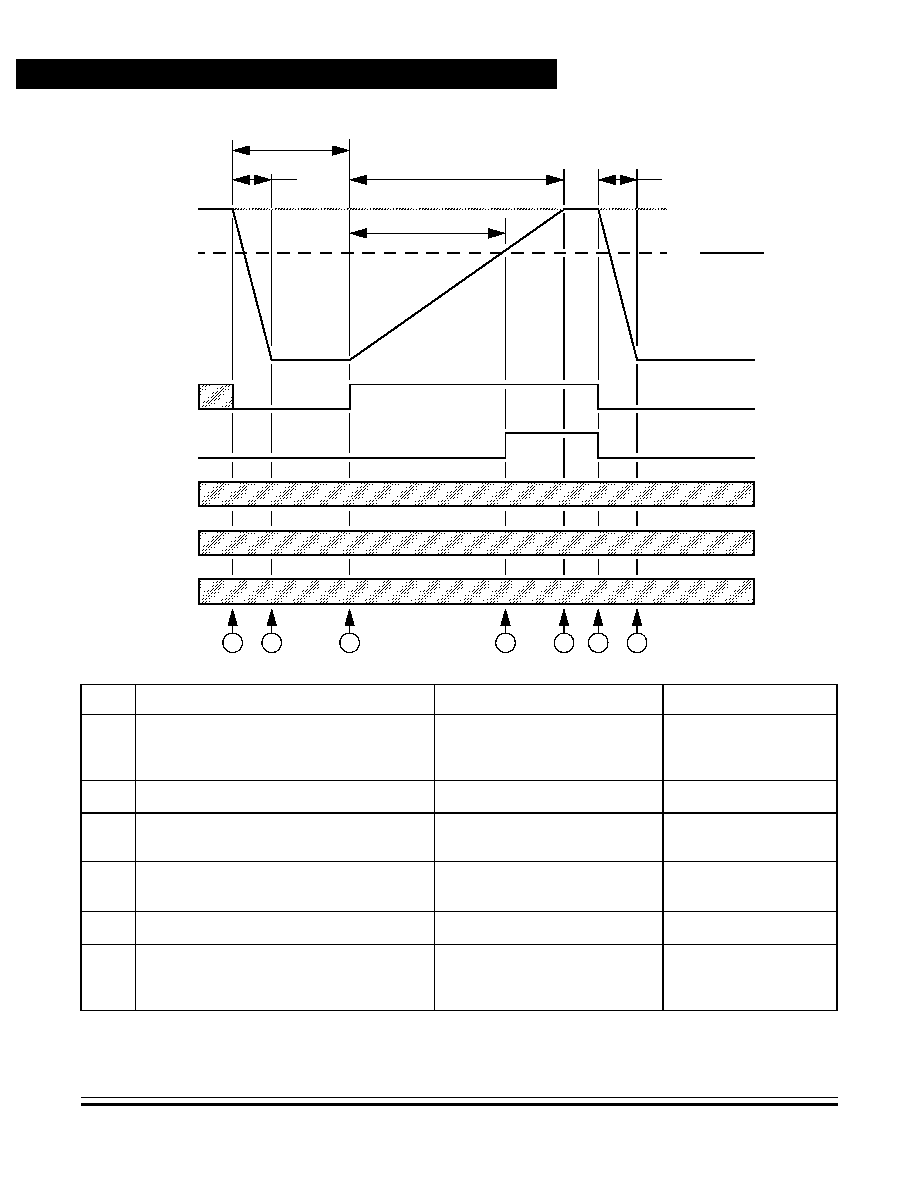
Advance Information
MC68HC705JJ7 ∑ MC68HC705JP7 -- REV 4
128
Analog Subsystem
MOTOROLA
Analog Subsystem
Figure 8-8. A/D Conversion -- Full Manual Control (Mode 0)
t
DIS
(MIN)
t
CHG
x I
CHG
C
EXT
t
CHG
t
DIS
V
X
=
t
MAX
V
MAX
CHG
COMP2
0
TOF
OCF
ICF
(MIN)
V
CAP
t
DIS
V
X
2
3
4
1
5
1
Point
Action
Software/Hardware Action
Dependent Variable(s)
0
Begin initial discharge and select mode 0
by clearing the CHG, ATD2, and ATD1
control bits in the ACR.
Software write
Software
1
V
CAP
falls to V
SS
.
Wait out minimum t
DIS
time.
V
MAX
, I
DIS
, C
EXT
2
Stop discharge and begin charge by setting
CHG control bit in ACR.
Software write
Software
3
V
CAP
rises to V
X
and comparator 2 output
trips, setting CPF2 and CMP2.
Wait out t
CHG
time.
V
X
, I
CHG
, C
EXT
4
V
CAP
reaches V
MAX
.
None
V
MAX
, I
CHG
, C
EXT
5
Begin next discharge by clearing the CHG
control bit in the ACR. Reset CPF2 by
writing a 1 to CPFR2.
Software write
Software
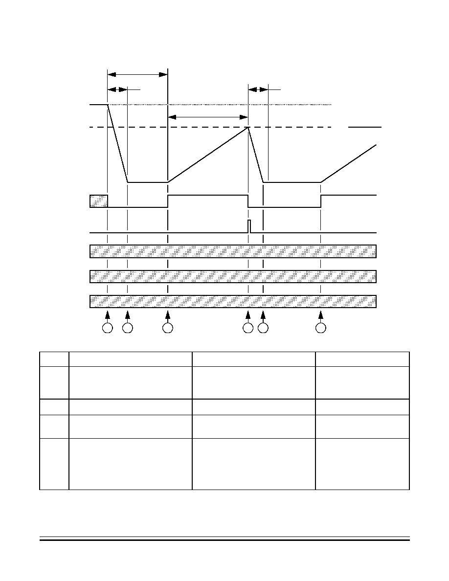
Analog Subsystem
A/D Conversion Methods
MC68HC705JJ7 ∑ MC68HC705JP7 -- REV 4
Advance Information
MOTOROLA
Analog Subsystem
129
Figure 8-9. A/D Conversion -- Manual/Auto Discharge Control (Mode 1)
t
DIS
(MIN)
t
CHG
x I
CHG
C
EXT
t
CHG
t
DIS
V
X
=
V
MAX
CHG
COMP2
0
TOF
OCF
ICF
(MIN)
V
CAP
t
DIS
V
X
1
2
3
1
2
Point
Action
Software/Hardware Action
Dependent Variable(s)
0
Begin initial discharge and select
mode 1 by clearing CHG and ATD2
and setting ATD1 in the ACR.
Software write
Software
1
V
CAP
falls to V
SS
.
Wait out minimum t
DIS
time.
V
MAX
, I
DIS
, C
EXT
2
Stop discharge and begin charge by
setting CHG control bit in ACR.
Software write
Software
3
V
CAP
rises to V
X
and comparator 2
output trips, setting CPF2 and
CMP2, which clears CHG control bit
in the ACR. Reset CPF2 by writing a
1 to CPFR2.
Wait out t
CHG
time.
CPF2 clears CHG control bit.
V
X
, I
CHG
, C
EXT
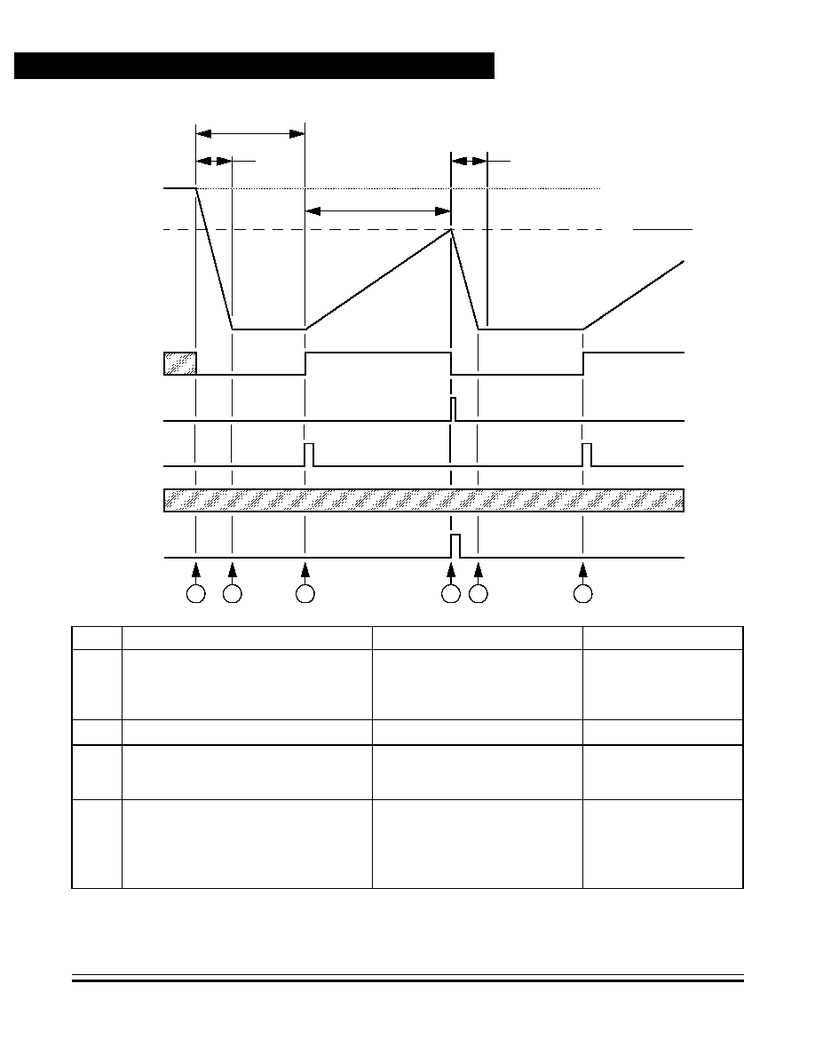
Advance Information
MC68HC705JJ7 ∑ MC68HC705JP7 -- REV 4
130
Analog Subsystem
MOTOROLA
Analog Subsystem
Figure 8-10. A/D Conversion -- TOF/ICF Control (Mode 2)
t
DIS
(MIN)
t
CHG
x I
CHG
C
EXT
t
CHG
t
DIS
V
X
=
V
MAX
CHG
COMP2
0
TOF
OCF
ICF
(MIN)
V
CAP
t
DIS
V
X
1
2
3
1
2
(TCAP)
Point
Action
Software/Hardware Action
Dependent Variable(s)
0
Begin initial discharge and select mode 2
by clearing CHG and ATD1 and setting
ATD2 in the ACR. Also set ICEN bit in
ACR and IEDG bit in TCR.
Software write
Software
1
V
CAP
falls to V
SS
.
Wait out minimum t
DIS
time.
V
MAX
, I
DIS
, C
EXT
2
Stop discharge and begin charge when
the next TOF sets the CHG control bit in
ACR.
Timer TOF sets the CHG control
bit in the ACR.
Free-running timer
counter overflow, f
OSC
3
V
CAP
rises to V
X
and comparator 2
output trips, setting CPF2 and CMP2,
which causes an ICF from the timer and
clears the CHG control bit in ACR. Must
clear CPF2 to trap next CPF2 flag.
Wait out t
CHG
time.
Timer ICF clears the CHG control
bit in the ACR.
V
X
, I
CHG
, C
EXT

Analog Subsystem
A/D Conversion Methods
MC68HC705JJ7 ∑ MC68HC705JP7 -- REV 4
Advance Information
MOTOROLA
Analog Subsystem
131
Figure 8-11. A/D Conversion -- OCF/ICF Control (Mode 3)
t
DIS
(MIN)
t
CHG
x I
CHG
C
EXT
t
CHG
t
DIS
V
X
=
V
MAX
CHG
COMP2
0
TOF
OCF
ICF
(MIN)
V
CAP
t
DIS
V
X
1
2
3
1
2
(TCAP)
Point
Action
Software/Hardware Action
Dependent Variable(s)
0
Begin initial discharge and select mode 3
by clearing CHG and setting ATD2 and
ATD1 in the ACR. Also set ICEN bit in
ACR and IEDG bit in TCR.
Software write
Software
1
V
CAP
falls to V
SS
. Set timer output
compare registers (OCRH and OCRL) to
desired charge start time.
Wait out minimum t
DIS
time.
Software write to OCRH, OCRL
V
MAX
, I
DIS
, C
EXT
,
software
2
Stop discharge and begin charge when
the next OCF sets the CHG control bit in
ACR.
Timer OCF sets the CHG control
bit in the ACR.
Free-running timer
output compare, f
OSC
3
V
CAP
rises to V
X
and comparator 2
output trips, setting CPF2 and CMP2,
which causes an ICF from the timer and
clears the CHG control bit in ACR. Must
clear CPF2 to trap next CPF2 flag. Load
next OCF.
Wait out t
CHG
time.
Timer ICF clears the CHG control
bit in the ACR.
V
X
, I
CHG
, C
EXT

Advance Information
MC68HC705JJ7 ∑ MC68HC705JP7 -- REV 4
132
Analog Subsystem
MOTOROLA
Analog Subsystem
8.7 Voltage Measurement Methods
The methods for obtaining a voltage measurement can use software
techniques to express these voltages as absolute or ratiometric
readings.
In most applications the external capacitor, the clock source, the
reference voltage, and the charging current may vary between devices
and with changes in supply voltage or ambient temperature. All of these
variations must be considered when determining the desired resolution
of the measurement. The maximum and minimum extremes for the full
scale count will be:
N
FSMIN
= C
EXTMIN
x V
FSMIN
x f
OSCMIN
/ (P x I
CHGMAX
)
N
FSMAX
= C
EXTMAX
x V
FSMAX
x f
OSCMAX
/ (P x I
CHGMIN
)
The minimum count should be the desired resolution, and the counting
mechanism must be capable of counting to the maximum. The final
scaling of the count will be by a math routine which calculates:
V
X
= V
REF
x (N
X
≠ N
OFF
) / (N
REF
≠ N
OFF
)
Where:
V
REF
= Known reference voltage
V
X
= Unknown voltage between V
SS
and V
REF
N
X
= Conversion count for unknown voltage
N
REF
= Conversion count for known reference voltage (V
REF
)
N
OFF
= Conversion count for minimum reference voltage (V
SS
)
When V
REF
is a stable voltage source such as a zener or other reference
source, then the unknown voltage will be determined as an absolute
reading. If V
REF
is the supply source to the device (V
DD
), then the
unknown voltage will be determined as a ratio of V
DD
, or a ratiometric
reading.
If the unknown voltage applied to the comparator is greater than its
common-mode range (V
DD
≠1.5 volts), then the external capacitor will
try to charge to the same level. This will cause both comparator inputs to
be above the common-mode range and the output of the comparator will

Analog Subsystem
Voltage Measurement Methods
MC68HC705JJ7 ∑ MC68HC705JP7 -- REV 4
Advance Information
MOTOROLA
Analog Subsystem
133
be indeterminate. In this case the comparator output flags may also be
set even if the actual voltage on the positive input (+) is less than the
voltage on the negative input (≠). All A/D conversion methods should
have a maximum time check to determine if this case is occurring.
Once the maximum timeout detection has been made, the state of the
comparator outputs can be tested to determine the situation. However,
such tests should be carefully designed when using modes 1, 2, or 3 as
these modes cause the immediate automatic discharge of the external
ramping capacitor before any software check can be made of the output
state of comparator 2.
NOTE:
All A/D conversion methods should include a test for a maximum
elapsed time to detect error cases where the inputs may be outside of
the design specification.
8.7.1 Absolute Voltage Readings
The absolute value of a voltage measurement can be calculated in
software by first taking a reference reading from a fixed source and then
comparing subsequent unknown voltages to that reading as a
percentage of the reference voltage multiplied times the known
reference value.
The accuracy of absolute readings will depend on the error sources
taken into account using the features of the analog subsystem and
appropriate software as described in
Table 8-6
. As can be seen from this
table, most of the errors can be reduced by frequent comparisons to a
known voltage, use of the inverted comparator inputs, and averaging of
multiple samples.
8.7.1.1 Internal Absolute Reference
If a stable source of V
DD
is provided, the reference measurement point
can be internally selected. In this case, the reference reading can be
taken by setting the V
REF
bit and clearing the MUX1:4 bits in the AMUX
register. This connects the channel selection bus to the V
DD
pin. To stay
within the V
MAX
range, the DHOLD bit should be used to select the 1/2
divided input.
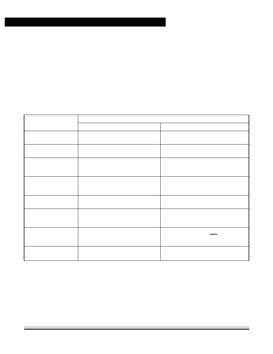
Advance Information
MC68HC705JJ7 ∑ MC68HC705JP7 -- REV 4
134
Analog Subsystem
MOTOROLA
Analog Subsystem
8.7.1.2 External Absolute Reference
If a stable external source is provided, the reference measurement point
can be any one of the channel selected pins from PB1≠PB4. In this case
the reference reading can be taken by setting the MUX bit in the AMUX
which connects channel selection bus to the pin connected to the
external reference source. If the external reference is greater than
V
DD
≠1.5 volts, then the DHOLD bit should be used to select the 1/2
divided input.
8.7.2 Ratiometric Voltage Readings
The ratiometric value of a voltage measurement can be calculated in
software by first taking a reference reading from a reference source and
then comparing subsequent unknown voltages to that reading as a
percentage of the reference value. The accuracy of ratiometric readings
Table 8-6. Absolute Voltage Reading Errors
Error Source
Accuracy Improvements Possible
In Hardware
In Software
Change in reference
voltage
Provide closer tolerance reference
Calibration and storage of reference source
over temperature and supply voltage
Change in magnitude of
ramp current source
Not adjustable
Compare unknown with recent
measurement from reference
Non-linearity of ramp
current source vs.
voltage
Not adjustable
Calibration and storage of voltages at 1/4,
1/2, 3/4, and FS
Frequency shift in
internal low-power
oscillator
Use external oscillator with crystal
Compare unknown with recent
measurement from reference
Sampling capacitor
leakage
Use faster conversion times
Compare unknown with recent
measurement from reference
Internal voltage divider
ratio
Not adjustable
Compare unknown with recent
measurement from reference OR avoid use
of divided input
Input offset voltage of
comparator 2
Not adjustable
Sum two readings on reference or
unknown using INV and INV control bit and
divide by 2 (average of both)
Noise internal to MCU
Close decoupling at V
DD
and V
SS
pins
and reduce supply source impedance
Average multiple readings on both the
reference and the unknown voltage

Analog Subsystem
Voltage Measurement Methods
MC68HC705JJ7 ∑ MC68HC705JP7 -- REV 4
Advance Information
MOTOROLA
Analog Subsystem
135
will depend on the variety of sources, but will generally be better than for
absolute readings. Many of these error sources can be taken into
account using the features of the analog subsystem and appropriate
software as described in
Table 8-7
. As with absolute measurements,
most of the errors can be reduced by frequent comparisons to the
reference voltage, use of the inverted comparator inputs, and averaging
of multiple samples.
8.7.2.1 Internal Ratiometric Reference
If readings are to be ratiometric to V
DD
, the reference measurement
point can be internally selected. In this case the reference reading can
be taken by setting the V
REF
bit and clearing the MUX1:4 bits in the
AMUX register which connects the channel selection bus to the V
DD
pin.
In order to stay within the V
MAX
range, the DHOLD bit should be used to
select the 1/2 divided input.
Table 8-7. Ratiometric Voltage Reading Errors
Error Source
Accuracy Improvements Possible
In Hardware
In Software
Change in reference
voltage
Not required for ratiometric
Compare unknown with recent
measurement from reference
Change in magnitude of
ramp current source
Not adjustable
Compare unknown with recent
measurement from reference
Non-linearity of ramp
current source vs. voltage
Not adjustable
Calibration and storage of voltages at
1/4, 1/2, 3/4, and FS
Frequency shift in internal
low-power oscillator
Not required for ratiometric
Compare unknown with recent
measurement from reference
Sampling capacitor leakage Use faster conversion times
Compare unknown with recent
measurement from reference
Internal voltage divider ratio
Not adjustable
Compare unknown with recent
measurement from reference
Input offset voltage of
comparator 2
Not adjustable
Sum two readings on reference or
unknown using INV and INV control bit
and divide by 2 (average of both)
Noise internal to MCU
Close decoupling at V
DD
and V
SS
pins
and reduce supply source impedance
Average multiple readings on both the
reference and the unknown voltage

Advance Information
MC68HC705JJ7 ∑ MC68HC705JP7 -- REV 4
136
Analog Subsystem
MOTOROLA
Analog Subsystem
8.7.2.2 External Ratiometric Reference
If readings are to be ratiometric to some external source, the reference
measurement point can be connected to any one of the channel selected
pins from PB1≠PB4. In this case, the reference reading can be taken by
setting the MUX bit in the AMUX which connects channel selection bus
to the pin connected to the external reference source. If the external
reference is greater than V
DD
≠1.5 volts, then the DHOLD bit should be
used to select the 1/2 divided input.
8.8 Voltage Comparator Features
The two internal comparators can be used as simple voltage
comparators if set up as described in
Table 8-8
. Both comparators can
be active in the wait mode and can directly restart the part by means of
the analog interrupt. Both comparators can also be active in the stop
mode, but cannot directly restart the part. However, the comparators can
directly drive PB4 which can then be connected externally to activate
either a port interrupt on the PA0:3 pins or the IRQ/V
PP
pin.
8.8.1 Voltage Comparator 1
Voltage comparator 1 is always connected to two of the port B I/O pins.
These pins should be configured as inputs and have their software
programmable pulldowns disabled. Also, the negative input of voltage
comparator 1 is connected to the PB3/AN3/TCAP and shared with the
input capture function of the 16-bit programmable timer. Therefore, the
timer input capture interrupt should be disabled so that changes in the
Table 8-8. Voltage Comparator Setup Conditions
Comparator
Current
Source
Enable
Discharge
Device
Disable
Port B Pin
as Inputs
Port B Pin
Pulldowns
Disabled
Prog. Timer
Input
Capture
Source
1
Not
affected
Not
affected
DDRB2 = 0
DDRB3 = 0
PDIB2 = 1
PDIB3 = 1
Not
affected
2
ISEN = 0
ISEN = 0
DDRB0 = 0
DDRB1 = 0
PDIB0 = 1
PDIB1 = 1
ICEN = 0
IEDG = 1
Analog Subsystem
Voltage Comparator Features
MC68HC705JJ7 ∑ MC68HC705JP7 -- REV 4
Advance Information
MOTOROLA
Analog Subsystem
137
voltage on the PB3/AN3/TCAP pin do not cause unwanted input capture
interrupts.
The output of comparator 1 can be connected to the port logic driving the
PB4/AN4/TCMP/CMP1 pin such that the output of the comparator is
ORed with the PB4 data bit and the OLVL bit from the 16-bit timer. This
capability requires that the OPT bit is set in the COPR at location $1FF0
as in
Figure 8-12
, and the COE1 bit is set in the ASR at location $001E.
OPT -- Optional Features Bit
The OPT bit enables two additional features: direct drive by
comparator 1 output to PB4 and voltage offset capability to sample
capacitor in analog subsystem.
1 = Optional features enabled
0 = Optional features disabled
8.8.2 Voltage Comparator 2
Voltage comparator 2 can be used as a simple comparator if its charge
current source and discharge device are disabled by clearing the ISEN
bit in the ACR. If the ISEN bit is set, the internal ramp discharge device
connected to PB0/AN0 may become active and try to pull down any
voltage source that may be connected to that pin. Also, since voltage
comparator 2 is always connected to two of the port B I/O pins, these
pins should be configured as inputs and have their software
programmable pulldowns disabled.
Address:
$1FF0
Bit 7
6
5
4
3
2
1
Bit 0
Read:
EPMSEC
OPT
Write:
COPC
Reset:
U
U
U
U
U
U
U
U
= Unimplemented
U = Unaffected
Figure 8-12. COP and Security Register (COPR)

Advance Information
MC68HC705JJ7 ∑ MC68HC705JP7 -- REV 4
138
Analog Subsystem
MOTOROLA
Analog Subsystem
8.9 Current Source Features
The internal current source connected to the PB0/AN0 pin supplies
about 100
µ
A of current when the discharge device is disabled and the
current source is active. Therefore, this current source can be used in an
application if the ISEN enable bit is set to power up the current source
and by setting the A/D conversion method to manual mode 0 (ATD1 and
ATD2 cleared) and the charge current enabled (CHG set).
8.10 Internal Temperature Sensing Diode Features
An internal diode is forward biased to V
SS
and will have its voltage
change, V
D
, for each degree centigrade rise in the temperature of the
device. This temperature sensing diode is powered up from a current
source only during the time that the diode is selected. When on, this
current source typically adds about 30
µ
A to the I
DD
current.
The temperature sensing diode can be selected by setting both the
HOLD and DHOLD bits in the AMUX register (see
8.3 Analog Multiplex
Register
).
8.11 Sample and Hold
When using the internal sample capacitor to capture a voltage for later
conversion, the HOLD or DHOLD bit must be cleared first before
changing any channel selection. If both the HOLD (or DHOLD) bit and
the channel selection are changed on the same write cycle, the sample
may be corrupted during the switching transitions.
NOTE:
The sample capacitor can be affected by excessive noise created with
respect to the device's V
SS
pin such that it may appear to leak down or
charge up depending on the voltage level stored on the sample
capacitor. It is recommended to avoid switching large currents through
the port pins while a voltage is to remain stored on the sample capacitor.
The additional option of adding an offset voltage to the bottom of the
sample capacitor allows unknown voltages near V
SS
to be sampled and
then shifted up past the comparator offset and the device offset caused

Analog Subsystem
Port B Interaction with Analog Inputs
MC68HC705JJ7 ∑ MC68HC705JP7 -- REV 4
Advance Information
MOTOROLA
Analog Subsystem
139
by a single V
SS
return pin. This offset also provides a means to measure
the internal V
SS
level regardless of the comparator offset to determine
N
OFF
as described in
8.7 Voltage Measurement Methods
. In either
case the OPT bit must be set in the COPR located at $1FF0 as in
Figure 8-12
and the VOFF bit must be set in the ASR. It is not necessary
to switch the VOFF bit during conversions, since the offset is controlled
by the HOLD and DHOLD bits when the VOFF is active. Refer to
8.3 Analog Multiplex Register
for more details on the design and
decoding of the sample and hold circuit.
8.12 Port B Interaction with Analog Inputs
The analog subsystem is connected directly to the port B I/O pins without
any intervening gates. It is, therefore, possible to measure the voltages
on port B pins set as inputs or to have the analog voltage measurements
corrupted by port B pins set as outputs.
8.13 Port B Pins as Inputs
All the port B pins will power up as inputs or return to inputs after a reset
of the device since the bits in the port B data direction register will be
reset.
If any port B pins are to be used for analog voltage measurements, they
should be left as inputs. In this case, not only can the voltage on the pin
be measured, but the logic state of the port B pins can be read from
location $0002.
8.14 Port B Pulldowns
All the port B pins have internal software programmable pulldown
devices available dependent on the state of the SWPDI bit in the mask
option register (MOR).
If the pulldowns are enabled, they will create an approximate 100
µ
A
load to any analog source connected to the pin. In some cases, the
analog source may be able to supply this current without causing any

Advance Information
MC68HC705JJ7 ∑ MC68HC705JP7 -- REV 4
140
Analog Subsystem
MOTOROLA
Analog Subsystem
error due to the analog source output impedance. Since this may not
always be true, it is therefore best to disable port B pulldowns on those
pins used for analog input sources.
8.15 Noise Sensitivity
In addition to the normal effects of electrical noise on the analog input
signal there can also be other noise-related effects caused by the
digital-to-analog interface. Since there is only one V
SS
return for both the
digital and the analog subsystems on the device, currents in the digital
section may affect the analog ground reference within the device. This
can add voltage offsets to measured inputs or cause channel-to-channel
crosstalk.
To reduce the impact of these effects, there should be no switching of
heavy I/O currents to or from the device while there is a critical analog
conversion or voltage comparison in process. Limiting switched I/O
currents to 2≠4 mA during these times is recommended.
A noise reduction benefit can be gained with 0.1-
µ
F bypass capacitors
from each analog input (PB4:1) to the V
SS
pin. Also, try to keep all the
digital power supply or load currents from passing through any
conductors which are the return paths for an analog signal.

MC68HC705JJ7 ∑ MC68HC705JP7 -- REV 4
Advance Information
MOTOROLA
Simple Synchronous Serial Interface
141
Advance Information -- MC68HC705JJ7/MC68HC705JP7
Section 9. Simple Synchronous Serial Interface
9.1 Contents
9.2
Introduction . . . . . . . . . . . . . . . . . . . . . . . . . . . . . . . . . . . . . . . 141
9.3
SIOP Signal Format . . . . . . . . . . . . . . . . . . . . . . . . . . . . . . . . 143
9.3.1
Serial Clock (SCK) . . . . . . . . . . . . . . . . . . . . . . . . . . . . . . . 143
9.3.2
Serial Data Input (SDI) . . . . . . . . . . . . . . . . . . . . . . . . . . . . 144
9.3.3
Serial Data Output (SDO). . . . . . . . . . . . . . . . . . . . . . . . . . 144
9.4
SIOP Registers . . . . . . . . . . . . . . . . . . . . . . . . . . . . . . . . . . . .145
9.4.1
SIOP Control Register (SCR). . . . . . . . . . . . . . . . . . . . . . . 145
9.4.2
SIOP Status Register . . . . . . . . . . . . . . . . . . . . . . . . . . . . .148
9.4.3
SIOP Data Register . . . . . . . . . . . . . . . . . . . . . . . . . . . . . . 149
9.2 Introduction
The simple synchronous serial I/O port (SIOP) subsystem is designed to
provide efficient serial communications with peripheral devices or other
MCUs. SIOP is implemented as a 3-wire master/slave system with serial
clock (SCK), serial data input (SDI), and serial data output (SDO). A
block diagram of the SIOP is shown in
Figure 9-1
.
The SIOP subsystem shares its input/output pins with port B. When the
SIOP is enabled (SPE bit set in the SCR), the port B data direction and
data registers are bypassed by the SIOP. The port B data direction and
data registers will remain accessible and can be altered by the
application software, but these actions will not affect the SIOP
transmitted or received data.
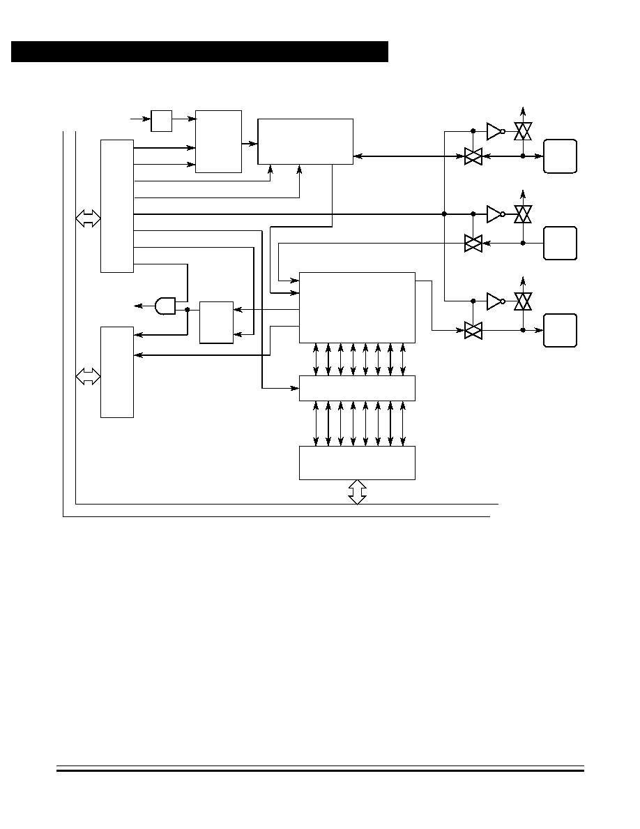
Advance Information
MC68HC705JJ7 ∑ MC68HC705JP7 -- REV 4
142
Simple Synchronous Serial Interface
MOTOROLA
Simple Synchronous Serial Interface
Figure 9-1. SIOP Block Diagram
PORTB LOGIC
SIOP
INTERRUPT
PB7
SCK
PB6
SDI
PB5
SDO
SD
R0
SD
R1
SD
R2
SD
R3
SD
R4
SD
R5
SD
R6
SD
R7
SIOP
IN
T
E
R
N
A
L
M
6
8H
C
0
5
BU
S
SPE
SI
OP
CO
NT
RO
L R
E
G
I
ST
ER
(S
CR)
SPIE
DATA REGISTER
(SDR)
DCOL
SIO
P
ST
ATU
S
R
E
G
I
ST
ER
(S
SR
)
SPIF
FORMAT CONTROL
SPIR
8-BIT SHIFT
LSBF
LATCH
S
R
REGISTER
DIN
DOUT
CLK
CLOCK
CONTROL
MSTR
CPHA
SPR1
SPR0
CLOCK
DIVIDER
OSCILLATOR
CLOCK
Q
(LSB OR MSB FIRST)
PORTB LOGIC
PORTB LOGIC
AND
SELECT
D0
D1
D2
D3
D4
D5
D6
D7
INTERNAL M68HC05 BUS
COMP
ERROR
˜
2
$000A
$000B
$000C

Simple Synchronous Serial Interface
SIOP Signal Format
MC68HC705JJ7 ∑ MC68HC705JP7 -- REV 4
Advance Information
MOTOROLA
Simple Synchronous Serial Interface
143
9.3 SIOP Signal Format
The SIOP subsystem can be software configured for master or slave
operation. No external mode selection inputs are available (for instance,
no slave select pin).
9.3.1 Serial Clock (SCK)
The state of the SCK output remains a fixed logic level during idle
periods between data transfers. The edges of SCK indicate the
beginning of each output data transfer and latch any incoming data
received. The first bit of transmitted data is output from the SDO pin on
the first falling edge of SCK. The first bit of received data is accepted at
the SDI pin on the first rising edge of SCK after the first falling edge. The
transfer is terminated upon the eighth rising edge of SCK.
The idle state of the SCK is determined by the state of the CPHA bit in
the SCR. When the CPHA is clear, SCK will remain idle at a logic 1 as
shown in
Figure 9-2
. When the CPHA is set, SCK will remain idle at a
logic 0 as shown in
Figure 9-3
. In both cases, the SDO changes data on
the falling edge of the SCK, and the SDI latches data in on the rising
edge of SCK.
Figure 9-2. SIOP Timing Diagram (CPHA = 0)
SCK
SDO
SDI
100 ns
100 ns
BIT 1
BIT 2
BIT 3
BIT 4
BIT 5
BIT 6
BIT 7
BIT 8
BIT 1
BIT 2
BIT 3
BIT 4
BIT 5
BIT 6
BIT 7
BIT 8
(CPHA = 0)
(IDLE = 1)
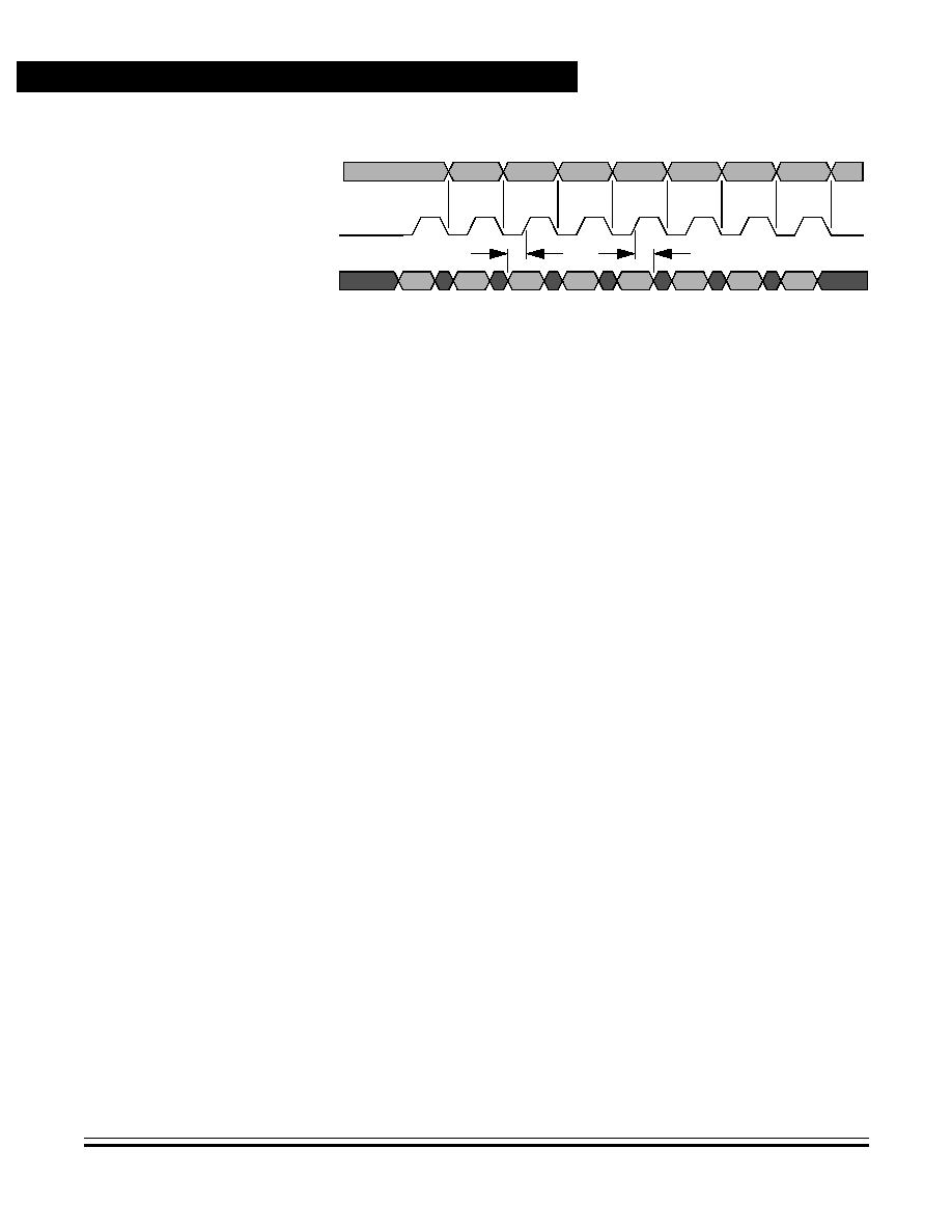
Advance Information
MC68HC705JJ7 ∑ MC68HC705JP7 -- REV 4
144
Simple Synchronous Serial Interface
MOTOROLA
Simple Synchronous Serial Interface
Figure 9-3. SIOP Timing Diagram (CPHA = 1)
The only difference in the master and slave modes of operation is the
sourcing of the SCK. In master mode, SCK is driven from an internal
source within the MCU. In slave mode, SCK is driven from a source
external to the MCU. The SCK frequency is based on one of four
divisions of the oscillator clock that is selected by the SPR0 and SPR1
bits in the SCR.
9.3.2 Serial Data Input (SDI)
The SDI pin becomes an input as soon as the SIOP subsystem is
enabled. New data is presented to the SDI pin on the falling edge of
SCK. Valid data must be present at least 100 nanoseconds before the
rising edge of SCK and remain valid for 100 nanoseconds after the rising
edge of SCK. See
Figure 9-3
.
9.3.3 Serial Data Output (SDO)
The SDO pin becomes an output as soon as the SIOP subsystem is
enabled. The state of the PB5/SDO pin reflects the value of the first bit
received on the previous transmission. Prior to enabling the SIOP, the
PB5/SDO can be initialized to determine the beginning state. While
SIOP is enabled, the port B logic cannot be used as a standard output
since that pin is connected to the last stage of the SIOP serial shift
register. A control bit (LSBF) is included in the SCR to allow the data to
be transmitted in either the MSB first format or the LSB first format.
SCK
SDO
SDI
100 ns
100 ns
BIT 1
BIT 2
BIT 3
BIT 4
BIT 5
BIT 6
BIT 7
BIT 8
BIT 1
BIT 2
BIT 3
BIT 4
BIT 5
BIT 6
BIT 7
BIT 8
(CPHA = 1)
(IDLE = 0)

Simple Synchronous Serial Interface
SIOP Registers
MC68HC705JJ7 ∑ MC68HC705JP7 -- REV 4
Advance Information
MOTOROLA
Simple Synchronous Serial Interface
145
The first data bit will be shifted out to the SDO pin on the first falling edge
of the SCK. The remaining data bits will be shifted out to the SDI pin on
subsequent falling edges of SCK. The SDO pin will present valid data at
least 100 nanoseconds before the rising edge of the SCK and remain
valid for 100 nanoseconds after the rising edge of SCK. See
Figure 9-3
.
9.4 SIOP Registers
The SIOP is programmed and controlled by the SIOP control register
(SCR) located at address $000A, the SIOP status register (SSR) located
at address $000B, and the SIOP data register (SDR) located at address
$000C.
9.4.1 SIOP Control Register (SCR)
The SIOP control register (SCR) is located at address $000A and
contains seven control bits and a write-only reset of the interrupt flag.
Figure 9-4
shows the position of each bit in the register and indicates the
value of each bit after reset.
SPIE -- Serial Peripheral Interrupt Enable Bit
The SPIE bit enables the SIOP to generate an interrupt whenever the
SPIF flag bit in the SSR is set. Clearing the SPIE bit will not affect the
state of the SPIF flag bit and will not terminate a serial interrupt once
the interrupt sequence has started. Reset clears the SPIE bit.
1 = Serial interrupt enabled
0 = Serial interrupt disabled
Address:
$000A
Bit 7
6
5
4
3
2
1
Bit 0
Read:
SPIE
SPE
LSBF
MSTR
0
CPHA
SPR1
SPR0
Write:
SPIR
Reset:
0
0
0
0
0
0
0
0
Figure 9-4. SIOP Control Register (SCR)

Advance Information
MC68HC705JJ7 ∑ MC68HC705JP7 -- REV 4
146
Simple Synchronous Serial Interface
MOTOROLA
Simple Synchronous Serial Interface
NOTE:
If the SPIE bit is cleared just after the serial interrupt sequence has
started (for instance, the CPU status is being stacked), then the CPU will
be unable to determine the source of the interrupt and will vector to the
reset vector as a default.
SPE -- Serial Peripheral Enable Bit
The SPE bit switches the port B interface such that SDO/PB5 is the
serial data output, SDI/PB6 is the serial data input, and SCK/PB7 is a
serial clock input in the slave mode or a serial clock output in the
master mode. The port B DDR and data registers can be manipulated
as usual, but these actions will not affect the transmitted or received
data. The SPE bit is readable and writable at any time, but clearing
the SPE bit while a transmission is in progress will 1) abort the
transmission, 2) reset the serial bit counter, and 3) convert port B to a
general-purpose I/O port. Reset clears the SPE bit.
1 = Serial peripheral enabled (port B I/O disabled)
0 = Serial peripheral disabled (port B I/O enabled)
LSBF -- Least Significant Bit First Bit
The LSBF bit controls the format of the transmitted and received data
to be transferred LSB or MSB first. Reset clears this bit.
1 = LSB transferred first
0 = MSB transferred first
MSTR -- Master Mode Select Bit
The MSTR bit configures the serial I/O port for master mode. A
transfer is initiated by writing to the SDR. Also, the SCK pin becomes
an output providing a synchronous data clock dependent upon the
divider of the oscillator frequency selected by the SPR0:1 bits. When
the device is in master mode, the SDO and SDI pins do not change
function. These pins behave exactly the same in both the master and
slave modes. The MSTR bit is readable and writable at any time
regardless of the state of the SPE bit. Clearing the MSTR bit will abort
any transfers that may have been in progress. Reset clears the MSTR
bit, placing the SIOP subsystem in slave mode.
1 = SIOP set up as master, SCK is an output
0 = SIOP set up as slave, SCK is an input

Simple Synchronous Serial Interface
SIOP Registers
MC68HC705JJ7 ∑ MC68HC705JP7 -- REV 4
Advance Information
MOTOROLA
Simple Synchronous Serial Interface
147
SPIR -- Serial Peripheral Interrupt Reset Bit
The SPIR bit is a write-only control to reset the SPIF flag bit in the
SSR. Reading the SPIR bit will return a logic 0.
1 = Reset the SPIF flag bit
0 = No effect
CPHA -- Clock Phase Bit
The CPHA bit controls the clock timing and phase in the SIOP. Data
is changed on the falling edge of SCK and data is captured (read) on
the rising edge of SCK. This bit is cleared by reset.
1 = SCK is idle low
0 = SCK is idle high
SPR0:1 -- Serial Peripheral Clock Rate Select Bits
The SPR0 and SPR1 bits select one of four clock rates given in
Table 9-1
to be supplied on the PB7/SCK pin when the device is
configured with the SIOP as a master (MSTR = 1). The fastest rate is
when both SPR0 and SPR1 are set. Both the SPR0 and SPR1 bits
are cleared by reset, which places the SIOP clock selection at the
slowest rate.
Table 9-1. SIOP Clock Rate Selection
SPR1
SPR0
SIOP Clock Rate
Oscillator Frequency
Divided by:
0
0
64
0
1
32
1
0
16
1
1
8

Advance Information
MC68HC705JJ7 ∑ MC68HC705JP7 -- REV 4
148
Simple Synchronous Serial Interface
MOTOROLA
Simple Synchronous Serial Interface
9.4.2 SIOP Status Register
The SIOP status register (SSR) is located at address $000B and
contains two read-only bits.
Figure 9-5
shows the position of each bit in
the register and indicates the value of each bit after reset.
SPIF -- Serial Port Interrupt Flag
The SPIF is a read-only status bit that is set on the last rising edge of
SCK and indicates that a data transfer has been completed. It has no
effect on any future data transfers and can be ignored. The SPIF bit
can be cleared by reading the SSR followed by a read or write of the
SDR or by writing a logic 1 to the SPIR bit in the SCR. If the SPIF is
cleared before the last rising edge of SCK it will be set again on the
last rising edge of SCK. Reset clears the SPIF bit.
1 = Serial transfer complete, serial interrupt if the SPIE bit in SCR
is set
0 = Serial transfer in progress or serial interface idle
DCOL -- Data Collision Bit
The DCOL is a read-only status bit which indicates that an illegal
access of the SDR has occurred. The DCOL bit will be set when
reading or writing the SDR after the first falling edge of SCK and
before SPIF is set. Reading or writing the SDR during this time will
result in invalid data being transmitted or received. The DCOL bit is
cleared by reading the SSR (when the SPIF bit is set) followed by a
read or write of the SDR. If the last part of the clearing sequence is
Address:
$000B
Bit 7
6
5
4
3
2
1
Bit 0
Read:
SPIF
DCOL
0
0
0
0
0
0
Write:
Reset:
0
0
0
0
0
0
0
0
= Unimplemented
Figure 9-5. SIOP Status Register (SSR)

Simple Synchronous Serial Interface
SIOP Registers
MC68HC705JJ7 ∑ MC68HC705JP7 -- REV 4
Advance Information
MOTOROLA
Simple Synchronous Serial Interface
149
done after another transfer has started, the DCOL bit will be set again.
Reset clears the DCOL bit.
1 = Illegal access of the SDR occurred
0 = No illegal access of the SDR detected
9.4.3 SIOP Data Register
The SIOP data register (SDR) is located at address $000C and serves
as both the transmit and receive data register. Writing to this register will
initiate a message transmission if the node is in master mode. The SIOP
subsystem is not double buffered and any write to this register will
destroy the previous contents. The SDR can be read at any time.
However, if a transfer is in progress the results may be ambiguous.
Writing to the SDR while a transfer is in progress can cause invalid data
to be transmitted and/or received.
Figure 9-6
shows the position of each
bit in the register. This register is not affected by reset.
Address:
$000C
Bit 7
6
5
4
3
2
1
Bit 0
Read:
Bit 7
6
5
4
3
2
1
Bit 0
Write:
Reset:
Unaffected by reset
Figure 9-6. SIOP Data Register (SDR)

Advance Information
MC68HC705JJ7 ∑ MC68HC705JP7 -- REV 4
150
Simple Synchronous Serial Interface
MOTOROLA
Simple Synchronous Serial Interface

MC68HC705JJ7 ∑ MC68HC705JP7 -- REV 4
Advance Information
MOTOROLA
Core Timer
151
Advance Information -- MC68HC705JJ7/MC68HC705JP7
Section 10. Core Timer
10.1 Contents
10.2
Introduction . . . . . . . . . . . . . . . . . . . . . . . . . . . . . . . . . . . . . . . 151
10.3
Core Timer Status and Control Register. . . . . . . . . . . . . . . . . 153
10.4
Core Timer Counter Register . . . . . . . . . . . . . . . . . . . . . . . . . 155
10.5
COP Watchdog. . . . . . . . . . . . . . . . . . . . . . . . . . . . . . . . . . . .156
10.2 Introduction
This section describes the operation of the core timer and the computer
operating properly (COP) watchdog as shown by the block diagram in
Figure 10-1
.
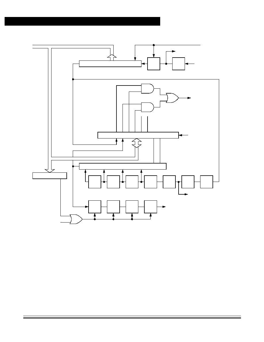
Advance Information
MC68HC705JJ7 ∑ MC68HC705JP7 -- REV 4
152
Core Timer
MOTOROLA
Core Timer
Figure 10-1. Core Timer Block Diagram
BITS 0≠7 OF 15-STAGE
IN
TE
RN
AL D
A
T
A
BU
S
RIPPLE COUNTER
COPR REGISTER
RTI RATE SELECT
˜
2
˜
2
˜
2
˜
2
˜
2
˜
2
˜
2
˜
2
RESET
COP
WATCHDOG
RESET
POWER-ON
RESET
INTERNAL CLOCK
˜
1024
CT
O
F
RT
I
F
CT
OFE
RT
I
E
CT
OF
R
RT
I
F
R
RT
1
RT
0
CORE TIMER
REQUEST
INTERRUPT
CORE TIMER STATUS/CONTROL REGISTER
CO
PC
˜
2
˜
2
˜
2
RESET
CORE TIMER COUNTER REGISTER
OVERFLOW
RESET
˜
4
OSC1
˜
2
INTERNAL
CLOCK
$0009
$0008
$1FF0

Core Timer
Core Timer Status and Control Register
MC68HC705JJ7 ∑ MC68HC705JP7 -- REV 4
Advance Information
MOTOROLA
Core Timer
153
10.3 Core Timer Status and Control Register
The read/write core timer status and control register (CTSCR) contains
the interrupt flag bits, interrupt enable bits, interrupt flag bit resets, and
the rate selects for the real-time interrupt as shown in
Figure 10-2
.
CTOF -- Core Timer Overflow Flag
This read-only flag becomes set when the first eight stages of the core
timer counter roll over from $FF to $00. The CTOF flag bit generates
a timer overflow interrupt request if CTOFE is also set. The CTOF flag
bit is cleared by writing a logic 1 to the CTOFR bit. Writing to CTOF
has no effect. Reset clears CTOF.
1 = Overflow in core timer has occurred.
0 = No overflow of core timer since CTOF last cleared
RTIF -- Real-Time Interrupt Flag
This read-only flag becomes set when the selected real-time interrupt
(RTI) output becomes active. RTIF generates a real-time interrupt
request if RTIE is also set. The RTIF enable bit is cleared by writing a
logic 1 to the RTIFR bit. Writing to RTIF has no effect. Reset clears
RTIF.
1 = Overflow in real-time counter has occurred.
0 = No overflow of real-time counter since RTIF last cleared
Address:
$0008
Bit 7
6
5
4
3
2
1
Bit 0
Read:
CTOF
RTIF
CTOFE
RTIE
0
0
RT1
RT0
Write:
CTOFR
RTIFR
Reset:
0
0
0
0
0
0
1
1
= Unimplemented
Figure 10-2. Core Timer Status and Control Register (CTSCR)

Advance Information
MC68HC705JJ7 ∑ MC68HC705JP7 -- REV 4
154
Core Timer
MOTOROLA
Core Timer
CTOFE -- Core Timer Overflow Interrupt Enable Bit
This read/write bit enables core timer overflow interrupts. Reset
clears CTOFE.
1 = Core timer overflow interrupts enabled
0 = Core timer overflow interrupts disabled
RTIE -- Real-Time Interrupt Enable Bit
This read/write bit enables real-time interrupts. Reset clears RTIE.
1 = Real-time interrupts enabled
0 = Real-time interrupts disabled
CTOFR -- Core Timer Overflow Flag Reset Bit
Writing a logic 1 to this write-only bit clears the CTOF bit. CTOFR
always reads as a logic 0. Reset does not affect CTOFR.
1 = Clear CTOF flag bit
0 = No effect on CTOF flag bit
RTIFR -- Real-Time Interrupt Flag Reset Bit
Writing a logic 1 to this write-only bit clears the RTIF bit. RTIFR
always reads as a logic 0. Reset does not affect RTIFR.
1 = Clear RTIF flag bit
0 = No effect on RTIF flag bit
RT1 and RT0 -- Real-Time Interrupt Select Bits 1 and 0
These read/write bits select one of four real-time interrupt rates, as
shown in
Table 10-1
. Because the selected RTI output drives the
COP watchdog, changing the real -time interrupt rate also changes
the counting rate of the COP watchdog. Reset sets RT1 and RT0,
selecting the longest COP timeout period and longest real-time
interrupt period.
NOTE:
Changing RT1 and RT0 when a COP timeout is imminent or uncertain
may cause a real-time interrupt request to be missed or an additional
real-time interrupt request to be generated. Clear the COP timer just
before changing RT1 and RT0.
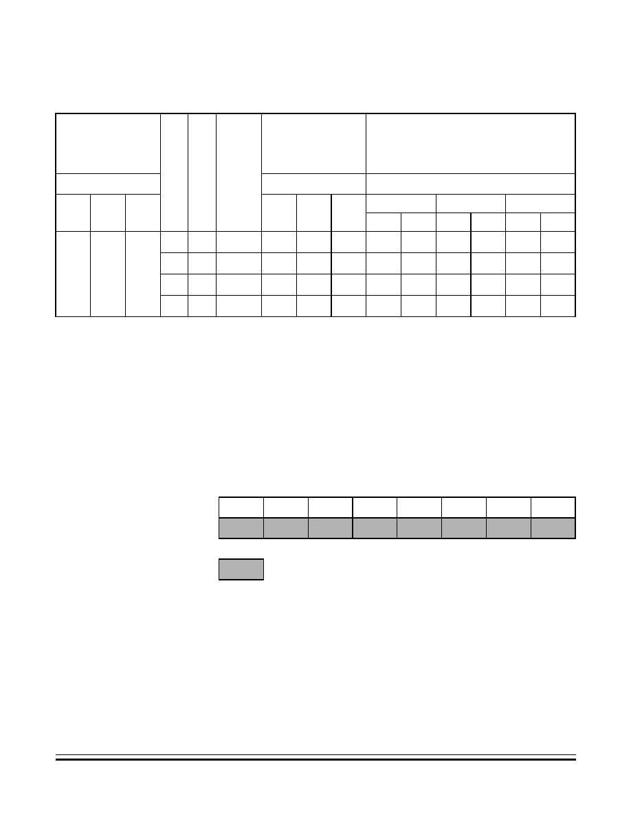
Core Timer
Core Timer Counter Register
MC68HC705JJ7 ∑ MC68HC705JP7 -- REV 4
Advance Information
MOTOROLA
Core Timer
155
10.4 Core Timer Counter Register
A 15-stage ripple counter driven by a divide-by-eight prescaler is the
basis of the core timer. The value of the first eight stages is readable at
any time from the read-only timer counter register as shown in
Figure 10-3
.
Power-on clears the entire counter chain and begins clocking the
counter. After the startup delay (16 or 4064 internal bus cycles
depending on the DELAY bit in the mask option register (MOR)), the
power-on reset circuit is released, clearing the counter again and
allowing the MCU to come out of reset.
Table 10-1. Core Timer Interrupt Rates and COP Timeout Selection
Timer Overflow
Interrupt Period
TOF = 1/(f
OSC
˜
2
11
)
(Microseconds)
RT1 RT0
RTI
Rate
= f
OSC
divided
by:
Real-Time
Interrupt Period
(RTI)
(Milliseconds)
COP Timeout Period
COP = 7-to-8 RTI Periods
(Milliseconds)
@ f
OSC
(MHz)
@ f
OSC
(MHz)
@ f
OSC
(MHz)
4.2
MHz
2.0
MHz
1.0
MHz
4.2
MHz
2.0
MHz
1.0
MHz
4.2 MHz
2.0 MHz
1.0 MHz
Min
Max
Min
Max
Min
Max
488
1024
2048
0
0
2
15
7.80
16.4
32.8
54.6
62.4
115
131
229
262
0
1
2
16
15.6
32.8
65.5
109
125
229
262
459
524
1
0
2
17
31.2
65.5
131
218
250
459
524
918
1049
1
1
2
18
62.4
131
262
437
499
918
1049
1835
2097
Address:
$0009
Bit 7
6
5
4
3
2
1
Bit 0
Read:
Bit 7
6
5
4
3
2
1
Bit 0
Write:
Reset:
0
0
0
0
0
0
0
0
= Unimplemented
Figure 10-3. Core Timer Counter Register (CTCR)
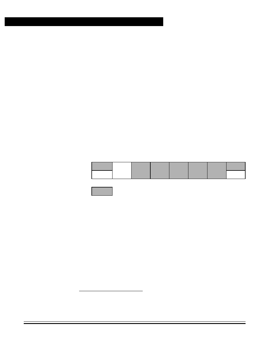
Advance Information
MC68HC705JJ7 ∑ MC68HC705JP7 -- REV 4
156
Core Timer
MOTOROLA
Core Timer
Each count of the timer counter register takes eight oscillator cycles or
four cycles of the internal bus. A timer overflow function at the eighth
counter stage allows a timer interrupt every 2048 oscillator clock cycles
or every 1024 internal bus cycles.
10.5 COP Watchdog
Four counter stages at the end of the core timer make up the computer
operating properly (COP) watchdog which can be enabled by the
COPEN bit in the MOR. The COP watchdog is a software error detection
system that automatically times out and resets the MCU if the COP
watchdog is not cleared periodically by a program sequence. Writing a
logic 0 to COPC bit in the COPR register clears the COP watchdog and
prevents a COP reset.
EPMSEC -- EPROM Security
(1)
Bit
The EPMSEC bit is a write-only security bit to protect the contents of
the user EPROM code stored in locations $0700≠$1FFF.
OPT -- Optional Features Bit
The OPT bit enables two additional features: direct drive by
comparator outputs to port A and voltage offset capability to sample
capacitor in analog subsystem.
1 = Optional features enabled
0 = Optional features disabled
Address:
$1FF0
Bit 7
6
5
4
3
2
1
Bit 0
Read:
OPT
Write:
EPMSEC
COPC
Reset:
Unaffected by reset
= Unimplemented
Figure 10-4. COP and Security Register (COPR)
1. No security feature is absolutely secure. However, Motorola's strategy is to make reading or
copying the EPROM/OTPROM difficult for unauthorized users.
Core Timer
COP Watchdog
MC68HC705JJ7 ∑ MC68HC705JP7 -- REV 4
Advance Information
MOTOROLA
Core Timer
157
COPC -- COP Clear Bit
This write-only bit resets the COP watchdog. The COP watchdog is
active in the run, wait, and halt modes of operation if the COP is
enabled by setting the COPEN bit in the MOR. The STOP instruction
disables the COP watchdog by clearing the counter and turning off its
clock source.
In applications that depend on the COP watchdog, the STOP
instruction can be disabled by setting the SWAIT bit in the MOR. In
applications that have wait cycles longer than the COP timeout
period, the COP watchdog can be disabled by clearing the COPEN
bit.
Table 10-2
summarizes recommended conditions for enabling
and disabling the COP watchdog.
NOTE:
If the voltage on the IRQ/V
PP
pin exceeds 1.5
◊
V
DD
, the COP watchdog
turns off and remains off until the IRQ/V
PP
pin voltage falls below
1.5
◊
V
DD
.
Table 10-2. COP Watchdog Recommendations
Voltage on
IRQ/V
PP
Pin
SWAIT
(in MOR)
(1)
1. The SWAIT bit in the MOR converts STOP instructions to HALT instructions.
Wait/Halt Time
Recommended COP
Watchdog Condition
Less than 1.5
◊
V
DD
1
Less than COP
timeout period
Enabled
(2)
2. Reset the COP watchdog immediately before executing the WAIT/HALT instruction.
Less than 1.5
◊
V
DD
1
Greater than COP
timeout period
Disabled
Less than 1.5
◊
V
DD
0
X
(3)
3. Don't care
Disabled
More than 1.5
◊
V
DD
X
X
(3)
Disabled

Advance Information
MC68HC705JJ7 ∑ MC68HC705JP7 -- REV 4
158
Core Timer
MOTOROLA
Core Timer

MC68HC705JJ7 ∑ MC68HC705JP7 -- REV 4
Advance Information
MOTOROLA
Programmable Timer
159
Advance Information -- MC68HC705JJ7/MC68HC705JP7
Section 11. Programmable Timer
11.1 Contents
11.2
Introduction . . . . . . . . . . . . . . . . . . . . . . . . . . . . . . . . . . . . . . . 160
11.3
Timer Registers . . . . . . . . . . . . . . . . . . . . . . . . . . . . . . . . . . . 162
11.4
Alternate Counter Registers . . . . . . . . . . . . . . . . . . . . . . . . . . 163
11.5
Input Capture Registers . . . . . . . . . . . . . . . . . . . . . . . . . . . . . 165
11.6
Output Compare Registers . . . . . . . . . . . . . . . . . . . . . . . . . . . 167
11.7
Timer Control Register . . . . . . . . . . . . . . . . . . . . . . . . . . . . . . 170
11.8
Timer Status Register . . . . . . . . . . . . . . . . . . . . . . . . . . . . . . . 171
11.9
Timer Operation during Wait Mode. . . . . . . . . . . . . . . . . . . . . 173
11.10 Timer Operation during Stop Mode . . . . . . . . . . . . . . . . . . . . 173
11.11 Timer Operation during Halt Mode . . . . . . . . . . . . . . . . . . . . . 173

Advance Information
MC68HC705JJ7 ∑ MC68HC705JP7 -- REV 4
160
Programmable Timer
MOTOROLA
Programmable Timer
11.2 Introduction
The MC68HC705JJ7/MC68HC705JP7 MCU contains a 16-bit
programmable timer with an input capture function and an output
compare function as shown by the block diagram in
Figure 11-1
.
The basis of the capture/compare timer is a 16-bit free-running counter
which increases in count with every four internal bus clock cycles. The
counter is the timing reference for the input capture and output compare
functions. The input capture and output compare functions provide a
means to latch the times at which external events occur, to measure
input waveforms, and to generate output waveforms and timing delays.
Software can read the value in the 16-bit free-running counter at any
time without affecting the counter sequence.
The input/output (I/O) registers for the input capture and output compare
functions are pairs of 8-bit registers, because of the 16-bit timer
architecture used. Each register pair contains the high and low bytes of
that function. Generally, accessing the low byte of a specific timer
function allows full control of that function; however, an access of the
high byte inhibits that specific timer function until the low byte is also
accessed.
Because the counter is 16 bits long and preceded by a fixed
divide-by-four prescaler, the counter rolls over every 262,144 internal
clock cycles (every 524,288 oscillator clock cycles). Timer resolution
with a 4-MHz crystal oscillator is 2 microseconds/count.
The interrupt capability, the input capture edge, and the output compare
state are controlled by the timer control register (TCR) located at $0012,
and the status of the interrupt flags can be read from the timer status
register (TSR) located at $0013.
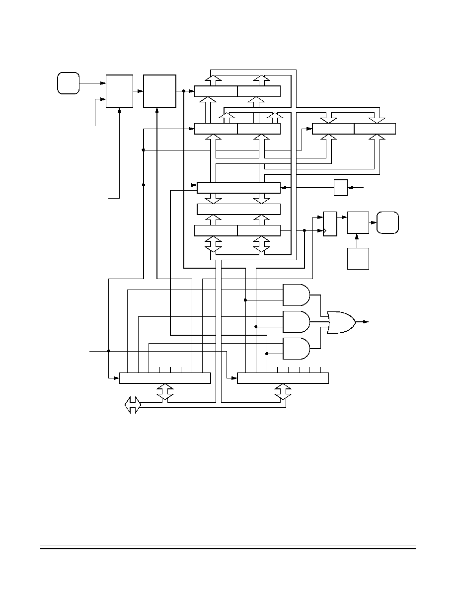
Programmable Timer
Introduction
MC68HC705JJ7 ∑ MC68HC705JP7 -- REV 4
Advance Information
MOTOROLA
Programmable Timer
161
Figure 11-1. Programmable Timer Overall Block Diagram
IE
DG
OL
VL
IC
IE
OC
IE
TO
I
E
TMRH ($0018)
TMRL ($0019)
16-BIT COUNTER
˜
4
INTERNAL
(OSC
˜
2)
TIMER CONTROL REGISTER
TIMER
REQUEST
OV
E
R
F
L
O
W
(
T
O
F
)
RESET
CLOCK
INTERRUPT
ACRH ($001A)
ACRL ($001B)
16-BIT COMPARATOR
OCRH ($0016)
OCRL ($0017)
PIN I/O
LOGIC
PB4
AN4
TCMP
PB3
AN3
TCAP
EDGE
SELECT
& DETECT
IC
F
OC
F
TO
F
TIMER STATUS REGISTER
IE
DG
IC
F
OC
F
OL
V
L
$0012
$0013
INTERNAL DATA BUS
LOGIC
INPUT
SELECT
MUX
CPF2
FLAG
ICEN
CONTROL
BIT
BIT
FROM
ANALOG
SUBSYSTEM
ICRH ($0014)
ICRL ($0015)
D
C
Q
ANALOG
COMP 1

Advance Information
MC68HC705JJ7 ∑ MC68HC705JP7 -- REV 4
162
Programmable Timer
MOTOROLA
Programmable Timer
11.3 Timer Registers
The functional block diagram of the 16-bit free-running timer counter and
timer registers is shown in
Figure 11-2
. The timer registers include a
transparent buffer latch on the LSB of the 16-bit timer counter.
Figure 11-2. Programmable Timer Block Diagram
The timer registers (TMRH and TMRL) shown in
Figure 11-3
are
read-only locations which contain the current high and low bytes of the
16-bit free-running counter. Writing to the timer registers has no effect.
Reset of the device presets the timer counter to $FFFC.
The TMRL latch is a transparent read of the LSB until a read of the
TMRH takes place. A read of the TMRH latches the LSB into the TMRL
location until the TMRL is again read. The latched value remains fixed
even if multiple reads of the TMRH take place before the next read of the
TMRL. Therefore, when reading the MSB of the timer at TMRH, the LSB
of the timer at TMRL must also be read to complete the read sequence.
During power-on reset (POR), the counter is initialized to $FFFC and
begins counting after the oscillator startup delay. Because the counter is
16 bits and preceded by a fixed prescaler, the value in the counter
repeats every 262,144 internal bus clock cycles (524,288 oscillator
cycles).
TO
I
E
TMRH ($0018)
TMR LSB
16-BIT COUNTER
˜
4
INTERNAL
(OSC
˜
2)
TIMER CONTROL REG.
TIMER
REQUEST
OVERFLOW (TOF)
RESET
CLOCK
INTERRUPT
TMRL ($0019)
TO
F
TIMER STATUS REG.
$0012
$0013
INTERNAL
$FFFC
DATA
READ
TMRH
READ
TMRL
READ
LATCH
BUS

Programmable Timer
Alternate Counter Registers
MC68HC705JJ7 ∑ MC68HC705JP7 -- REV 4
Advance Information
MOTOROLA
Programmable Timer
163
When the free-running counter rolls over from $FFFF to $0000, the timer
overflow flag bit (TOF) is set in the TSR. When the TOF is set, it can
generate an interrupt if the timer overflow interrupt enable bit (TOIE) is
also set in the TCR. The TOF flag bit can only be reset by reading the
TMRL after reading the TSR.
Other than clearing any possible TOF flags, reading the TMRH and
TMRL in any order or any number of times does not have any effect on
the 16-bit free-running counter.
NOTE:
To prevent interrupts from occurring between readings of the TMRH and
TMRL, set the I bit in the condition code register (CCR) before reading
TMRH and clear the I bit after reading TMRL.
11.4 Alternate Counter Registers
The functional block diagram of the 16-bit free-running timer counter and
alternate counter registers is shown in
Figure 11-4
. The alternate
counter registers behave the same as the timer registers, except that
any reads of the alternate counter will not have any effect on the TOF
Address:
$0018
Bit 7
6
5
4
3
2
1
Bit 0
Read:
Bit 15
14
13
12
11
10
9
Bit 8
Write:
Reset:
1
1
1
1
1
1
1
1
Address:
$0018
Bit 7
6
5
4
3
2
1
Bit 0
Read:
Bit 7
6
5
4
3
2
1
Bit 0
Write:
Reset:
1
1
1
1
1
1
0
0
= Unimplemented
Figure 11-3. Programmable Timer Registers (TMRH and TMRL)

Advance Information
MC68HC705JJ7 ∑ MC68HC705JP7 -- REV 4
164
Programmable Timer
MOTOROLA
Programmable Timer
flag bit and timer interrupts. The alternate counter registers include a
transparent buffer latch on the LSB of the 16-bit timer counter.
Figure 11-4. Alternate Counter Block Diagram
The alternate counter registers (ACRH and ACRL) shown in
Figure 11-5
are read-only locations which contain the current high and
low bytes of the 16-bit free-running counter. Writing to the alternate
counter registers has no effect. Reset of the device presets the timer
counter to $FFFC.
The ACRL latch is a transparent read of the LSB until a read of the
ACRH takes place. A read of the ACRH latches the LSB into the ACRL
location until the ACRL is again read. The latched value remains fixed
even if multiple reads of the ACRH take place before the next read of the
ACRL. Therefore, when reading the MSB of the timer at ACRH, the LSB
of the timer at ACRL must also be read to complete the read sequence.
During power-on reset (POR), the counter is initialized to $FFFC and
begins counting after the oscillator startup delay. Because the counter is
16 bits and preceded by a fixed prescaler, the value in the counter
repeats every 262,144 internal bus clock cycles (524,288 oscillator
cycles).
Reading the ACRH and ACRL in any order or any number of times does
not have any effect on the 16-bit free-running counter or the TOF flag bit.
NOTE:
To prevent interrupts from occurring between readings of the ACRH and
ACRL, set the I bit in the condition code register (CCR) before reading
ACRH and clear the I bit after reading ACRL.
ACRH ($001A)
TMR LSB
16-BIT COUNTER
˜
4
INTERNAL
(OSC
˜
2)
RESET
CLOCK
ACRL ($001B)
INTERNAL
$FFFC
DATA
READ
ACRH
READ
ACRL
READ
LATCH
BUS

Programmable Timer
Input Capture Registers
MC68HC705JJ7 ∑ MC68HC705JP7 -- REV 4
Advance Information
MOTOROLA
Programmable Timer
165
11.5 Input Capture Registers
The input capture function is a means to record the time at which an
event occurs. The source of the event can be the change on an external
pin (PB3/AN3/TCAP) or the CPF2 flag bit of voltage comparator 2 in the
analog subsystem. The ICEN bit in the analog subsystem control
register (ACR) at $001D selects which source is the input signal. When
the input capture circuitry detects an active edge on the selected source,
it latches the contents of the free-running timer counter registers into the
input capture registers as shown in
Figure 11-6
.
NOTE:
Both the ICEN bit in the ACR and the IEDG bit in the TCR must be set
when using voltage comparator 2 to trigger the input capture function.
Latching values into the input capture registers at successive edges of
the same polarity measures the period of the selected input signal.
Latching the counter values at successive edges of opposite polarity
measures the pulse width of the signal.
Address:
$001A
Bit 7
6
5
4
3
2
1
Bit 0
Read:
Bit 15
14
13
12
11
10
9
Bit 8
Write:
Reset:
1
1
1
1
1
1
1
1
Address:
$001B
Bit 7
6
5
4
3
2
1
Bit 0
Read:
Bit 7
6
5
4
3
2
1
Bit 0
Write:
Reset:
1
1
1
1
1
1
0
0
= Unimplemented
Figure 11-5. Alternate Counter Registers (ACRH and ACRL)

Advance Information
MC68HC705JJ7 ∑ MC68HC705JP7 -- REV 4
166
Programmable Timer
MOTOROLA
Programmable Timer
Figure 11-6. Timer Input Capture Block Diagram
The input capture registers are made up of two 8-bit read-only registers
(ICRH and ICRL) as shown in
Figure 11-7
. The input capture edge
detector contains a Schmitt trigger to improve noise immunity. The edge
that triggers the counter transfer is defined by the input edge bit (IEDG)
in the TCR. Reset does not affect the contents of the input capture
registers.
IC
I
E
ICRH ($0014)
16-BIT COUNTER
˜
4
INTERNAL
(OSC
˜
2)
TIMER CONTROL REG.
TIMER
REQUEST
INPUT CAPTURE (ICF)
RESET
CLOCK
INTERRUPT
ICRL ($0015)
IC
F
TIMER STATUS REG.
$0012
$0013
INTERNAL
$F
FFC
DATA
READ
ICRH
READ
ICRL
LATCH
BUS
IE
D
G
EDGE
SELECT
& DETECT
LOGIC
IED
G
PB3
AN3
TCAP
INPUT
SELECT
MUX
CPF2
FLAG
ICEN
CONTROL
BIT
BIT
FROM
ANALOG
SUBSYSTEM
INTERNAL
DATA
BUS
Address:
$0014
Bit 7
6
5
4
3
2
1
Bit 0
Read:
Bit 15
14
13
12
11
10
9
Bit 8
Write:
Reset:
Unaffected by reset
Address:
$0015
Bit 7
6
5
4
3
2
1
Bit 0
Read:
Bit 7
6
5
4
3
2
1
Bit 0
Write:
Reset:
Unaffected by reset
= Unimplemented
Figure 11-7. Input Capture Registers (ICRH and ICRL)

Programmable Timer
Output Compare Registers
MC68HC705JJ7 ∑ MC68HC705JP7 -- REV 4
Advance Information
MOTOROLA
Programmable Timer
167
The result obtained by an input capture will be one count higher than the
value of the free-running timer counter preceding the external transition.
This delay is required for internal synchronization. Resolution is affected
by the prescaler, allowing the free-running timer counter to increment
once every four internal clock cycles (eight oscillator clock cycles).
Reading the ICRH inhibits future captures until the ICRL is also read.
Reading the ICRL after reading the timer status register (TSR) clears the
ICF flag bit. There is no conflict between reading the ICRL and transfers
from the free-running timer counters. The input capture registers always
contain the free-running timer counter value which corresponds to the
most recent input capture.
NOTE:
To prevent interrupts from occurring between readings of the ICRH and
ICRL, set the I bit in the condition code register (CCR) before reading
ICRH and clear the I bit after reading ICRL.
11.6 Output Compare Registers
The output compare function is a means of generating an output signal
when the 16-bit timer counter reaches a selected value as shown in
Figure 11-8
. Software writes the selected value into the output compare
registers. On every fourth internal clock cycle (every eight oscillator
clock cycles) the output compare circuitry compares the value of the
free-running timer counter to the value written in the output compare
registers. When a match occurs, the timer transfers the output level
(OLVL) from the timer control register (TCR) to the PB4/AN4/TCMP pin.
Software can use the output compare register to measure time periods,
to generate timing delays, or to generate a pulse of specific duration
or a pulse train of specific frequency and duty cycle on the
PB4/AN4/TCMP pin.
The planned action on the PB4/AN4/TCMP pin depends on the value
stored in the OLVL bit in the TCR, and it occurs when the value of the
16-bit free-running timer counter matches the value in the output
compare registers shown in
Figure 11-9
. These registers are read/write
bits and are unaffected by reset.
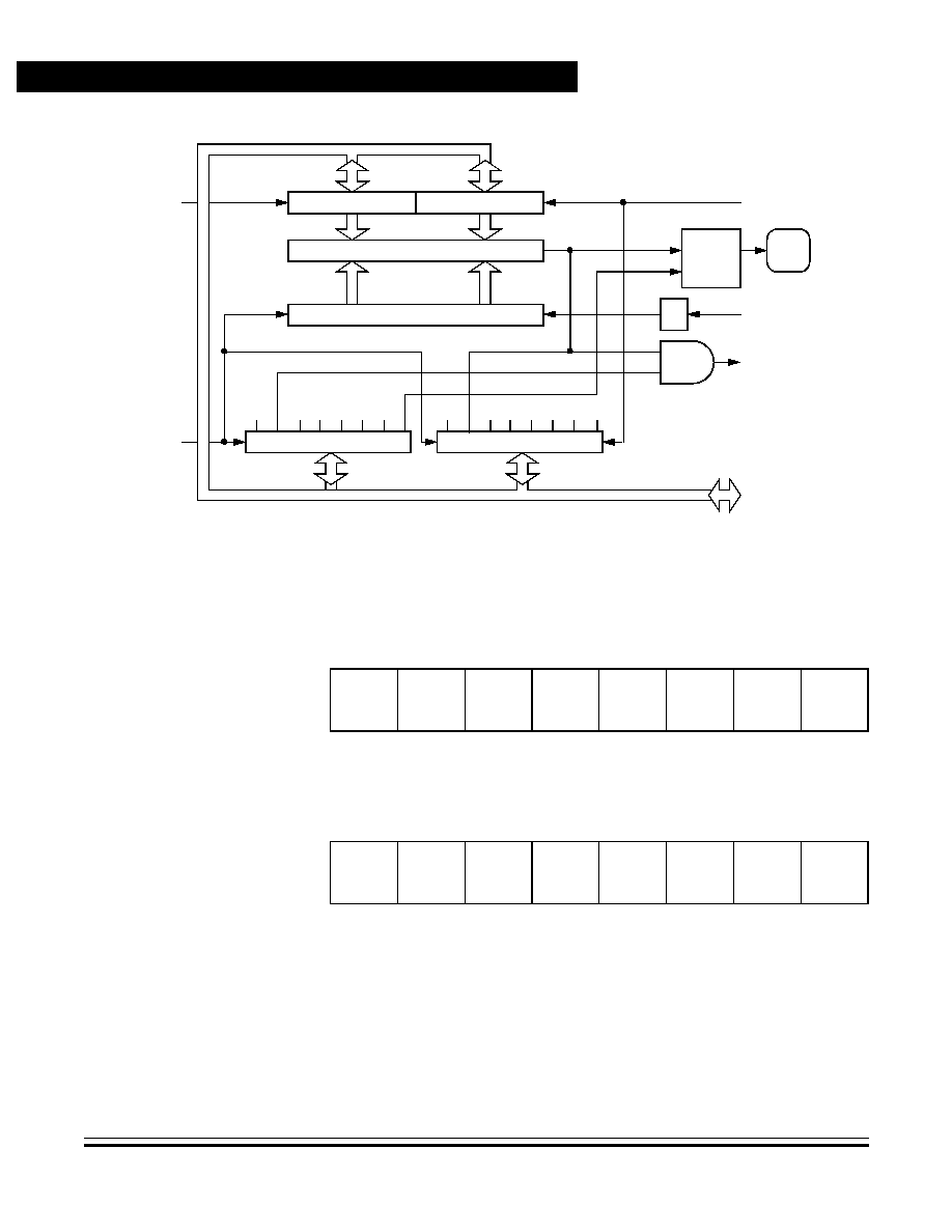
Advance Information
MC68HC705JJ7 ∑ MC68HC705JP7 -- REV 4
168
Programmable Timer
MOTOROLA
Programmable Timer
Figure 11-8. Timer Output Compare Block Diagram
OC
IE
OCRH ($0016)
16-BIT COUNTER
˜
4
INTERNAL
(OSC
˜
2)
TIMER CONTROL REG.
TIMER
REQUEST
OUTPUT COMPARE
RESET
CLOCK
INTERRUPT
OCRL ($0017)
OC
F
TIMER STATUS REG.
$0012
$0013
INTERNAL
$FFFC
DATA
R/W
OCRH
R/W
OCRL
BUS
OL
VL
PB4
AN4
TCMP
EDGE
SELECT
DETECT
LOGIC
OL
V
L
16-BIT COMPARATOR
(OCF)
Address:
$0016
Bit 7
6
5
4
3
2
1
Bit 0
Read:
Bit 15
14
13
12
11
10
9
Bit 8
Write:
Reset:
Unaffected by reset
Address:
$0017
Bit 7
6
5
4
3
2
1
Bit 0
Read:
Bit 7
6
5
4
3
2
1
Bit 0
Write:
Reset:
Unaffected by reset
Figure 11-9. Output Compare Registers (OCRH and OCRL)

Programmable Timer
Output Compare Registers
MC68HC705JJ7 ∑ MC68HC705JP7 -- REV 4
Advance Information
MOTOROLA
Programmable Timer
169
Writing to the OCRH before writing to the OCRL inhibits timer compares
until the OCRL is written. Reading or writing to the OCRL after reading
the TCR will clear the output compare flag bit (OCF). The output
compare OLVL state will be clocked to its output latch regardless of the
state of the OCF.
To prevent OCF from being set between the time it is read and the time
the output compare registers are updated, use this procedure:
1. Disable interrupts by setting the I bit in the condition code register.
2. Write to the OCRH. Compares are now inhibited until OCRL is
written.
3. Read the TSR to arm the OCF for clearing.
4. Enable the output compare registers by writing to the OCRL. This
also clears the OCF flag bit in the TSR.
5. Enable interrupts by clearing the I bit in the condition code register.
A software example of this procedure is shown in
Table 11-1
.
Table 11-1. Output Compare Initialization Example
9B
...
...
B7
B6
BF
...
...
9A
16
13
17
SEI
...
...
STA
LDA
STX
...
...
CLI
OCRH
TSR
OCRL
DISABLE INTERRUPTS
.....
.....
INHIBIT OUTPUT COMPARE
ARM OCF FLAG FOR CLEARING
READY FOR NEXT COMPARE, OCF CLEARED
.....
.....
ENABLE INTERRUPTS
Advance Information
MC68HC705JJ7 ∑ MC68HC705JP7 -- REV 4
170
Programmable Timer
MOTOROLA
Programmable Timer
11.7 Timer Control Register
The timer control register (TCR) shown in
Figure 11-10
, performs the
following functions:
∑
Enables input capture interrupts
∑
Enables output compare interrupts
∑
Enables timer overflow interrupts
∑
Controls the active edge polarity of the TCAP signal
∑
Controls the active level of the TCMP output
Reset clears all the bits in the TCR with the exception of the IEDG bit
which is unaffected.
ICIE -- Input Capture Interrupt Enable Bit
This read/write bit enables interrupts caused by an active signal on
the TCAP pin or from CPF2 flag bit of the analog subsystem voltage
comparator 2. Reset clears the ICIE bit.
1 = Input capture interrupts enabled
0 = Input capture interrupts disabled
OCIE -- Output Compare Interrupt Enable Bit
This read/write bit enables interrupts caused by an active match of the
output compare function. Reset clears the OCIE bit.
1 = Output compare interrupts enabled
0 = Output compare interrupts disabled
Address:
$0012
Bit 7
6
5
4
3
2
1
Bit 0
Read:
ICIE
OCIE
TOIE
0
0
0
IEDG
OLVL
Write:
Reset:
0
0
0
0
0
0
U
0
= Unimplemented
U = Unaffected
Figure 11-10. Timer Control Register (TCR)

Programmable Timer
Timer Status Register
MC68HC705JJ7 ∑ MC68HC705JP7 -- REV 4
Advance Information
MOTOROLA
Programmable Timer
171
TOIE -- Timer Overflow Interrupt Enable
This read/write bit enables interrupts caused by a timer overflow.
Reset clears the TOIE bit.
1 = Timer overflow interrupts enabled
0 = Timer overflow interrupts disabled
IEDG -- Input Capture Edge Select
The state of this read/write bit determines whether a positive or
negative transition triggers a transfer of the contents of the timer
register to the input capture register. This transfer can occur due to
transitions on the TCAP pin or the CPF2 flag bit of voltage comparator
2. Resets have no effect on the IEDG bit.
1 = Positive edge (low-to-high transition) triggers input capture
0 = Negative edge (high-to-low transition) triggers input capture
NOTE:
The IEDG bit must be set when either mode 2 or 3 of the analog
subsystem is being used for A/D conversions. Otherwise, the input
capture will not occur on the rising edge of the comparator 2 flag.
OLVL -- Output Compare Output Level Select
The state of this read/write bit determines whether a logic 1 or a logic
0 is transferred to the TCMP pin when a successful output compare
occurs. Reset clears the OLVL bit.
1 = Signal to TCMP pin goes high on output compare.
0 = Signal to TCMP pin goes low on output compare.
11.8 Timer Status Register
The timer status register (TSR) shown in
Figure 11-11
contains flags for
these events:
∑
An active signal on the TCAP pin or the CPF2 flag bit of voltage
comparator 2 in the analog subsystem, transferring the contents
of the timer registers to the input capture registers
∑
A match between the 16-bit counter and the output compare
registers, transferring the OLVL bit to the PB4/AN4/TCMP pin if
that pin is set as an output
∑
An overflow of the timer registers from $FFFF to $0000
Advance Information
MC68HC705JJ7 ∑ MC68HC705JP7 -- REV 4
172
Programmable Timer
MOTOROLA
Programmable Timer
Writing to any of the bits in the TSR has no effect. Reset does not
change the state of any of the flag bits in the TSR.
ICF -- Input Capture Flag
The ICF bit is automatically set when an edge of the selected polarity
occurs on the TCAP pin. Clear the ICF bit by reading the timer status
register with the ICF set, and then reading the low byte (ICRL, $0015)
of the input capture registers. Resets have no effect on ICF.
OCF -- Output Compare Flag
The OCF bit is automatically set when the value of the timer registers
matches the contents of the output compare registers. Clear the OCF
bit by reading the timer status register with the OCF set and then
accessing the low byte (OCRL, $0017) of the output compare
registers. Resets have no effect on OCF.
TOF -- Timer Overflow Flag
The TOF bit is automatically set when the 16-bit timer counter rolls
over from $FFFF to $0000. Clear the TOF bit by reading the timer
status register with the TOF set and then accessing the low byte
(TMRL, $0019) of the timer registers. Resets have no effect on TOF.
Address:
$0013
Bit 7
6
5
4
3
2
1
Bit 0
Read:
ICF
OCF
TOF
0
0
0
0
0
Write:
Reset:
U
U
U
0
0
0
0
0
= Unimplemented
U = Unaffected
Figure 11-11. Timer Status Register (TSR)

Programmable Timer
Timer Operation during Wait Mode
MC68HC705JJ7 ∑ MC68HC705JP7 -- REV 4
Advance Information
MOTOROLA
Programmable Timer
173
11.9 Timer Operation during Wait Mode
During wait mode, the 16-bit timer continues to operate normally and
may generate an interrupt to trigger the MCU out of wait mode.
11.10 Timer Operation during Stop Mode
When the MCU enters stop mode, the free-running counter stops
counting (the internal processor clock is stopped). It remains at that
particular count value until stop mode is exited by applying a low signal
to the IRQ/V
PP
pin, at which time the counter resumes from its stopped
value as if nothing had happened. If stop mode is exited via an external
reset (logic low applied to the RESET pin), the counter is forced to
$FFFC.
If a valid input capture edge occurs during stop mode, the input capture
detect circuitry will be armed. This action does not set any flags or wake
up the MCU, but when the MCU does wake up there will be an active
input capture flag (and data) from the first valid edge. If the stop mode is
exited by an external reset, no input capture flag or data will be present
even if a valid input capture edge was detected during stop mode.
11.11 Timer Operation during Halt Mode
When the MCU enters halt mode, the functions and states of the 16-bit
programmable timer are the same as for wait mode described in
11.9 Timer Operation during Wait Mode
.

Advance Information
MC68HC705JJ7 ∑ MC68HC705JP7 -- REV 4
174
Programmable Timer
MOTOROLA
Programmable Timer

MC68HC705JJ7 ∑ MC68HC705JP7 -- REV 4
Advance Information
MOTOROLA
Personality EPROM (PEPROM)
175
Advance Information -- MC68HC705JJ7/MC68HC705JP7
Section 12. Personality EPROM (PEPROM)
12.1 Contents
12.2
Introduction . . . . . . . . . . . . . . . . . . . . . . . . . . . . . . . . . . . . . . . 175
12.3
PEPROM Registers . . . . . . . . . . . . . . . . . . . . . . . . . . . . . . . . 177
12.3.1
PEPROM Bit Select Register . . . . . . . . . . . . . . . . . . . . . . . 177
12.3.2
PEPROM Status and Control Register. . . . . . . . . . . . . . . . 178
12.4
PEPROM Programming . . . . . . . . . . . . . . . . . . . . . . . . . . . . . 179
12.5
PEPROM Reading . . . . . . . . . . . . . . . . . . . . . . . . . . . . . . . . .180
12.6
PEPROM Erasing . . . . . . . . . . . . . . . . . . . . . . . . . . . . . . . . . . 181
12.2 Introduction
This section describes how to program the 64-bit personality erasable
programmable read-only memory (PEPROM).
Figure 12-1
shows the
structure of the PEPROM subsystem.
NOTE:
In packages with no quartz window, the PEPROM functions as one-time
programmable ROM (OTPROM).

Advance Information
MC68HC705JJ7 ∑ MC68HC705JP7 -- REV 4
176
Personality EPROM (PEPROM)
MOTOROLA
Personality EPROM (PEPROM)
Figure 12-1. Personality EPROM Block Diagram
PEPROM STATUS/CONTROL REGISTER
SINGLE
SENSE
AMPLIFIER
PE
D
A
T
A
0
0
0
0
0
PE
PG
M
PE
PR
ZF
8-TO-1 COLUMN DECODER
AND MULTIPLEXER
8-TO-1 ROW DECODER
AND MULTIPLEXER
CO
L 0
CO
L 1
CO
L 2
CO
L 3
CO
L 4
CO
L 5
CO
L 6
CO
L 7
ROW 0
ROW 1
ROW 2
ROW 3
ROW 4
ROW 5
ROW 6
ROW 7
V
PP
SWITCH
V
PP
SWITCH
PEPROM BIT SELECT REGISTER
0
0
PE
B5
PE
B4
PE
B3
PE
B2
PE
B1
PE
B0
ROW ZERO
DECODER
INTERNAL DATA BUS
INTERNAL DATA BUS
V
PP
RESET
RESET
$000F
$000E

Personality EPROM (PEPROM)
PEPROM Registers
MC68HC705JJ7 ∑ MC68HC705JP7 -- REV 4
Advance Information
MOTOROLA
Personality EPROM (PEPROM)
177
12.3 PEPROM Registers
Two I/O registers control programming and reading of the PEPROM:
∑
The PEPROM bit select register (PEBSR)
∑
The PEPROM status and control register (PESCR)
12.3.1 PEPROM Bit Select Register
The PEPROM bit select register (PEBSR) selects one of 64 bits in the
PEPROM array. Reset clears all the bits in the PEPROM bit select
register.
PEB7 and PEB6 -- Not connected to the PEPROM array
These read/write bits are available as storage locations. Reset clears
PEB7 and PEB6.
PEB5≠PEB0 -- PEPROM Bit Selects
These read/write bits select one of 64 bits in the PEPROM as shown
in
Table 12-1
. Bits PEB2≠0 select the PEPROM row, and bits
PEB5≠PEB3 select the PEPROM column. Reset clears PEB5≠PEB0,
selecting the PEPROM bit in row zero, column zero.
Address:
$000E
Bit 7
6
5
4
3
2
1
Bit 0
Read:
PEB7
PEB6
PEB5
PEB4
PEB3
PEB2
PEB1
PEB0
Write:
Reset:
0
0
0
0
0
0
0
0
Figure 12-2. PEPROM Bit Select Register (PEBSR)

Advance Information
MC68HC705JJ7 ∑ MC68HC705JP7 -- REV 4
178
Personality EPROM (PEPROM)
MOTOROLA
Personality EPROM (PEPROM)
12.3.2 PEPROM Status and Control Register
The PEPROM status and control register (PESCR) controls the
PEPROM programming voltage. This register also transfers the
PEPROM bits to the internal data bus and contains a flag bit when row
zero is selected.
PEDATA -- PEPROM Data Bit
This read-only bit is the output state of the PEPROM sense amplifier
and shows the state of the currently selected bit. The state of the
PEDATA bit does not affect the programming of the bit selected by the
PEBSR. Reset does not affect the PEDATA bit.
1 = PEPROM data is a logic 1.
0 = PEPROM data is a logic 0.
PEPGM -- PEPROM Program Control Bit
This read/write bit controls the switches that apply the programming
voltage from the IRQ/V
PP
pin to the selected PEPROM bit cell. When
the PEPGM bit is set, the selected bit cell will be programmed to a
logic 1, regardless of the state of the PEDATA bit. Reset clears the
PEPGM bit.
1 = Programming voltage applied to array bit
0 = Programming voltage not applied to array bit
PEPRZF -- PEPROM Row Zero Flag
This read-only bit is set when the PEPROM bit select register selects
the first row (row zero) of the PEPROM array. Selecting any other row
clears PEPRZF. Monitoring PEPRZF can reduce the code needed to
Address:
$000F
Bit 7
6
5
4
3
2
1
Bit 0
Read:
PEDATA
0
PEPGM
0
0
0
0
PEPRZF
Write:
R
R
R
Reset:
U
0
0
0
0
0
0
1
= Unimplemented
R
= Reserved
U = Unaffected
Figure 12-3. PEPROM Status and Control Register (PESCR)
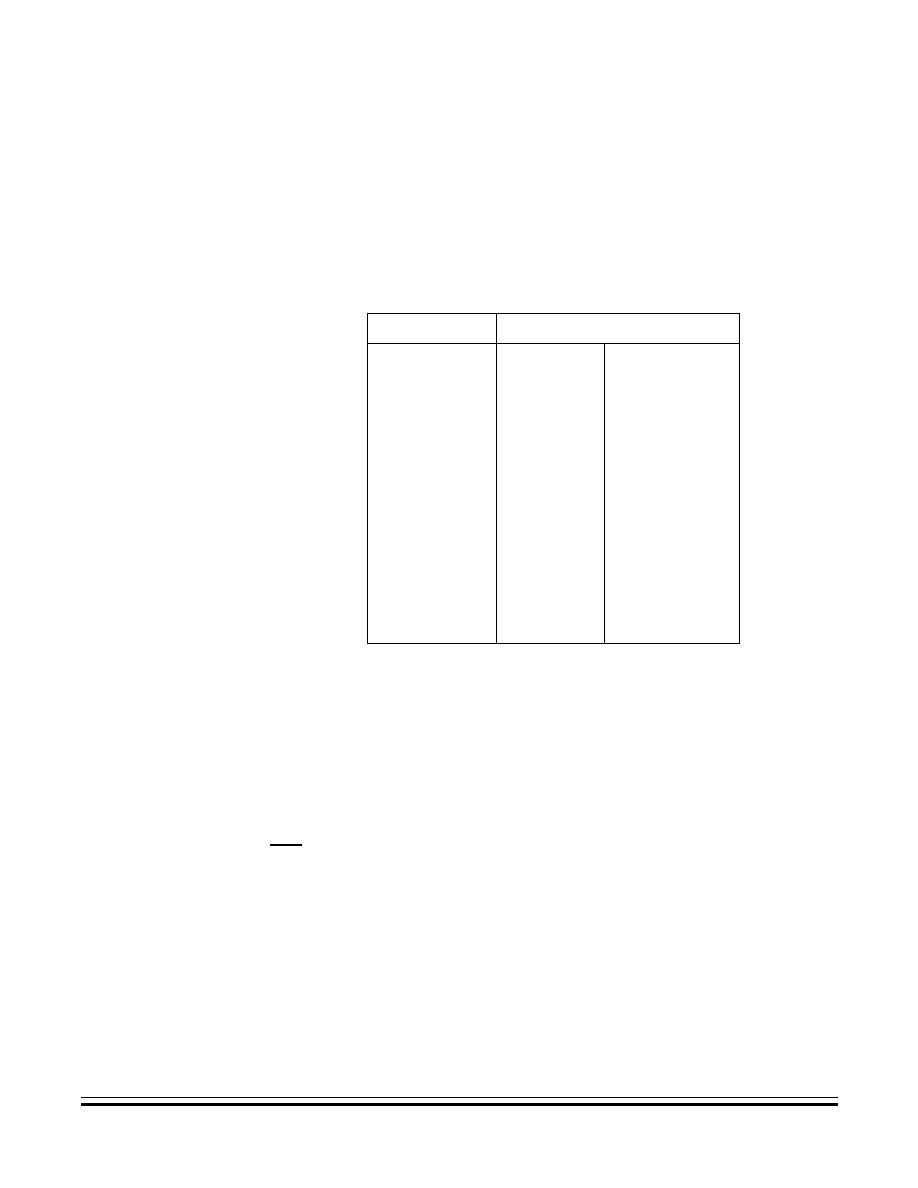
Personality EPROM (PEPROM)
PEPROM Programming
MC68HC705JJ7 ∑ MC68HC705JP7 -- REV 4
Advance Information
MOTOROLA
Personality EPROM (PEPROM)
179
access one byte of eight PEPROM locations. Reset clears the
PEPROM bit select register, thereby setting the PEPRZF bit by
default.
1 = Row zero selected
0 = Row zero not selected
12.4 PEPROM Programming
Factory-provided software for programming the PEPROM is available on
the World Wide Web at:
http://www.motorola.com/mcu/
NOTE:
While the PEPGM bit is set and the V
PP
voltage level is applied to the
IRQ/V
PP
pin, do not access bits that are to be left unprogrammed
(erased).
To program the PEPROM bits properly, the V
DD
voltage must be greater
than 4.5 Vdc.
Table 12-1. PEPROM Bit Selection
PEBSR
PEPROM Bit Selected
$00
$01
|
V
$07
$08
$09
|
V
$37
$38
$39
|
V
$3E
$3F
Row 0
Row 1
|
V
Row 7
Row 0
Row 1
|
V
Row 7
Row 0
Row 1
|
V
Row 6
Row 7
Column 0
Column 0
|
V
Column 0
Column 1
Column 1
|
V
Column 6
Column 7
Column 7
|
V
Column 7
Column 7

Advance Information
MC68HC705JJ7 ∑ MC68HC705JP7 -- REV 4
180
Personality EPROM (PEPROM)
MOTOROLA
Personality EPROM (PEPROM)
The PEPROM can also be programmed by user software with the V
PP
voltage level applied to the IRQ/V
PP
pin. This sequence shows how to
program each PEPROM bit:
1. Select a PEPROM bit by writing to the PEBSR.
2. Set the PEPGM bit in the PESCR.
3. Wait for the programming time, t
EPGM
.
4. Clear the PEPGM bit.
5. Move to next PEPROM bit to be programmed in step 1.
12.5 PEPROM Reading
This sequence shows how to read the PEPROM:
1. Select a bit by writing to the PEBSR.
2. Read the PEDATA bit in the PESCR.
3. Store the PEDATA bit in RAM or in a register.
4. Select another bit by changing the PEBSR.
5. Continue reading and storing the PEDATA bits until the required
personality EPROM data is retrieved and stored.
Reading the PEPROM is easiest when each PEPROM column contains
one byte. Selecting a row 0 bit selects the first bit, and incrementing the
PEPROM bit select register (PEBSR) selects the next bit in row 1 from
the same column. Incrementing PEBSR seven more times selects the
remaining bits of the column and ends up selecting the bit in row 0 of the
next column, thereby setting the row 0 flag, PEPRZF.
NOTE:
A PEPROM byte that has been read can be transferred to the personality
EPROM bit select register (PEBSR) as a temporary storage location
such that subsequent reads of the PEBSR quickly yield that PEPROM
byte.

Personality EPROM (PEPROM)
PEPROM Erasing
MC68HC705JJ7 ∑ MC68HC705JP7 -- REV 4
Advance Information
MOTOROLA
Personality EPROM (PEPROM)
181
12.6 PEPROM Erasing
MCUs with windowed packages permit PEPROM erasing with ultraviolet
light. Erase the PEPROM by exposing it to 15 Ws/cm
2
of ultraviolet light
with a wavelength of 2537 angstroms. Position the ultraviolet light
source 1 inch from the window. Do not use a shortwave filter. The erased
state of a PEPROM bit is a logic 0.

Advance Information
MC68HC705JJ7 ∑ MC68HC705JP7 -- REV 4
182
Personality EPROM (PEPROM)
MOTOROLA
Personality EPROM (PEPROM)

MC68HC705JJ7 ∑ MC68HC705JP7 -- REV 4
Advance Information
MOTOROLA
EPROM/OTPROM
183
Advance Information -- MC68HC705JJ7/MC68HC705JP7
Section 13. EPROM/OTPROM
13.1 Contents
13.2
Introduction . . . . . . . . . . . . . . . . . . . . . . . . . . . . . . . . . . . . . . . 183
13.3
EPROM Registers . . . . . . . . . . . . . . . . . . . . . . . . . . . . . . . . .184
13.3.1
EPROM Programming Register . . . . . . . . . . . . . . . . . . . . . 184
13.3.2
Mask Option Register . . . . . . . . . . . . . . . . . . . . . . . . . . . . .185
13.3.3
EPROM Security Bit . . . . . . . . . . . . . . . . . . . . . . . . . . . . . . 188
13.4
EPROM Programming . . . . . . . . . . . . . . . . . . . . . . . . . . . . . . 189
13.4.1
MOR Programming . . . . . . . . . . . . . . . . . . . . . . . . . . . . . . 189
13.4.2
EPMSEC Programming . . . . . . . . . . . . . . . . . . . . . . . . . . . 190
13.5
EPROM Erasing . . . . . . . . . . . . . . . . . . . . . . . . . . . . . . . . . . . 190
13.2 Introduction
This section describes how to program the 6160-byte erasable
programmable read-only memory/one-time programmable read-only
memory (EPROM/OTPROM), the mask option register (MOR), and the
EPROM security bit (EPMSEC).
NOTE:
In packages with no quartz window, the EPROM functions as one-time
programmable ROM (OTPROM).
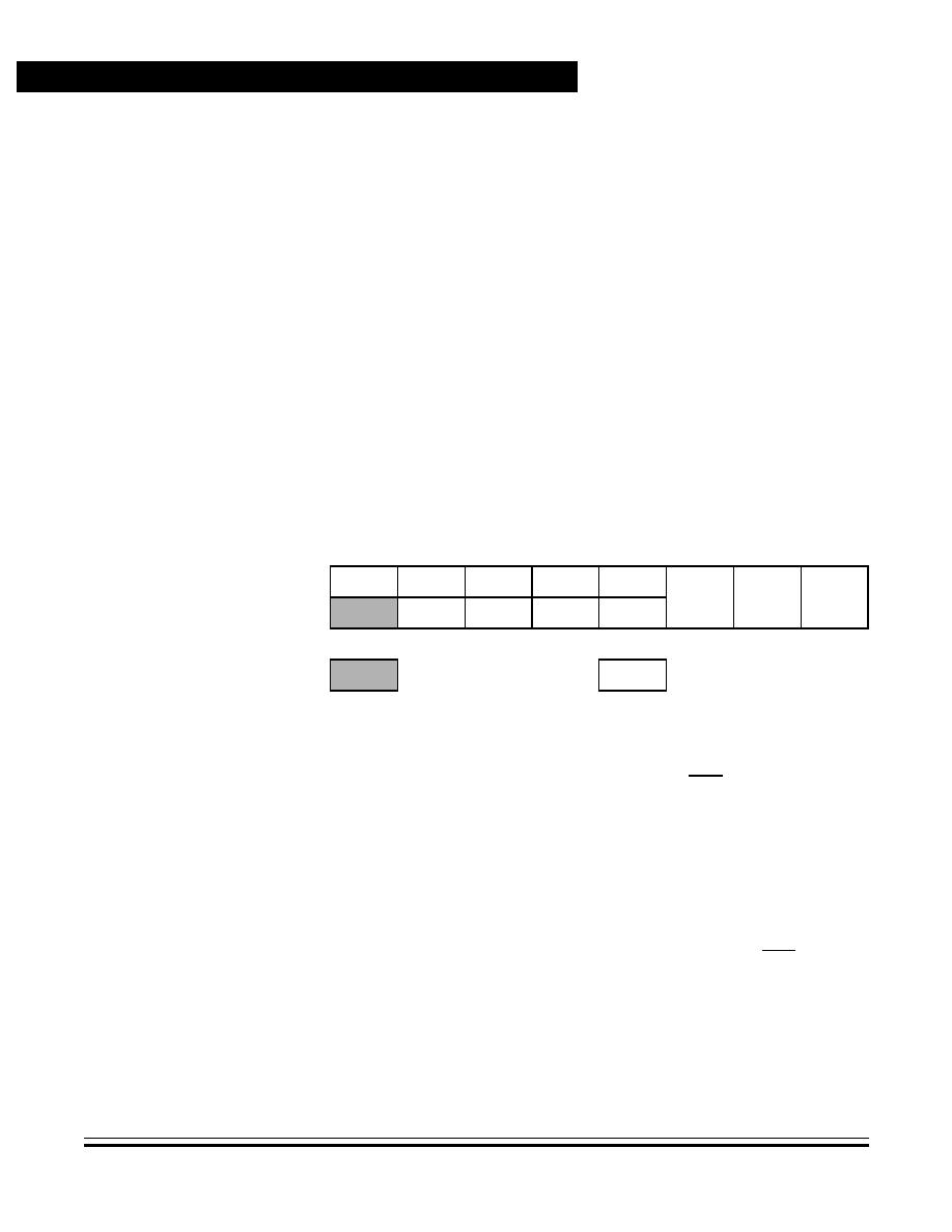
Advance Information
MC68HC705JJ7 ∑ MC68HC705JP7 -- REV 4
184
EPROM/OTPROM
MOTOROLA
EPROM/OTPROM
13.3 EPROM Registers
The EPROM programming register (EPROG) controls the actual
programming of the EPROM bytes and the mask option register (MOR).
The MOR controls eight mask options found on the read-only memory
(ROM) version of this microcontroller unit (MCU). There is an additional
EPROM bit (EPMSEC) located at the computer operating properly
(COP) address to provide EPROM array security.
13.3.1 EPROM Programming Register
The EPROM programming register (EPROG) shown in
Figure 13-1
contains the control bits for programming the EPROM. In normal
operation, the EPROM programming register contains all logic 0s.
EPGM -- EPROM Programming Bit
This read/write bit applies the voltage from the IRQ/V
PP
pin to the
EPROM. To write the EPGM bit, the ELAT bit must already be set.
Clearing the ELAT bit also clears the EPGM bit. Reset clears EPGM.
1 = EPROM programming power switched on
0 = EPROM programming power switched off
MPGM -- Mask Option Register (MOR) Programming Bit
This read/write bit applies programming power from the IRQ/V
PP
pin
to the MOR. Reset clears MPGM.
1 = MOR programming power switched on
0 = MOR programming power switched off
Address:
$001C
Bit 7
6
5
4
3
2
1
Bit 0
Read:
0
0
0
0
0
ELAT
MPGM
EPGM
Write:
R
R
R
R
Reset:
0
0
0
0
0
0
0
0
= Unimplemented
R
= Reserved for test
Figure 13-1. EPROM Programming Register (EPROG)

EPROM/OTPROM
EPROM Registers
MC68HC705JJ7 ∑ MC68HC705JP7 -- REV 4
Advance Information
MOTOROLA
EPROM/OTPROM
185
ELAT -- EPROM Bus Latch Bit
This read/write bit configures address and data buses for
programming the EPROM array. EPROM data cannot be read when
ELAT is set. Clearing the ELAT bit also clears the EPGM bit. Reset
clears ELAT.
1 = Address and data buses configured for EPROM programming
of the array. The address and data buses are latched in the
EPROM array when a subsequent write to the array is made.
Data in the EPROM array cannot be read.
0 = Address and data buses configured for normal operation
Whenever the ELAT bit is cleared, the EPGM bit is also cleared. Both the
EPGM and the ELAT bit cannot be set using the same write instruction.
Any attempt to set both the ELAT and EPGM bit on the same write
instruction cycle will result in the ELAT bit being set and the EPGM bit
being cleared. To program a byte of EPROM, manipulate the EPROG
register as follows:
1. Set the ELAT bit in the EPROG register.
2. Write the desired data to the desired EPROM address.
3. Set the EPGM bit in the EPROG register for the specified
programming time, t
EPGM
.
4. Clear the ELAT and EPGM bits in the EPROG register.
13.3.2 Mask Option Register
The mask option register (MOR) shown in
Figure 13-2
is an EPROM
byte that controls eight mask options. The MOR is unaffected by reset.
The erased state of the MOR is $00. The options that can be
programmed by the MOR are:
1. Port software programmable pulldown devices (enable or disable)
2. Startup delay after stop (16 or 4064 cycles)
3. Oscillator shunt resistor (2 M
or open)
4. STOP instruction (enable or disable)
5. Low-voltage reset (enable or disable)

Advance Information
MC68HC705JJ7 ∑ MC68HC705JP7 -- REV 4
186
EPROM/OTPROM
MOTOROLA
EPROM/OTPROM
6. Port A external interrupt function (enable or disable)
7. IRQ trigger sensitivity (edge-triggered only or both edge- and
level-triggered)
8. COP watchdog (enable or disable)
SWPDI -- Software Pulldown Inhibit Bit
This EPROM bit inhibits software control of the port A and port B
pulldown devices.
1 = Software pulldown inhibited
0 = Software pulldown enabled
DELAY -- Stop Startup Delay Bit
This EPROM bit selects the number of bus cycles that must elapse
before bus activity begins following a restart from the stop mode.
1 = Startup delay is 4064 bus cycles.
0 = Startup delay is 16 bus cycles.
CAUTION:
The 16-cycle delay option will work properly in devices with the internal
low-power oscillator or with a steady external clock source. Check
crystal/ceramic resonator specifications carefully before using the
16-cycle delay option with a crystal or ceramic resonator.
OSCRES -- Oscillator Resistor Bit
This EPROM bit configures the internal shunt resistor.
1 = Oscillator configured with 2 Mæ shunt resistor
0 = Oscillator configured without a shunt resistor
Address:
$1FF1
Bit 7
6
5
4
3
2
1
Bit 0
Read:
SWPDI
DELAY
OSCRES
SWAIT
LVREN
PIRQ
LEVEL
COPEN
Write:
Reset:
Unaffected by reset
Erased:
0
0
0
0
0
0
0
0
Figure 13-2. Mask Option Register (MOR)

EPROM/OTPROM
EPROM Registers
MC68HC705JJ7 ∑ MC68HC705JP7 -- REV 4
Advance Information
MOTOROLA
EPROM/OTPROM
187
NOTE:
The optional oscillator resistor is NOT recommended for devices that
use an external RC oscillator. For such devices, this bit should be left
erased as a 0.
SWAIT -- STOP Conversion to WAIT Bit
This EPROM bit disables the STOP instruction and prevents
inadvertently turning off the COP watchdog with a STOP instruction.
When the SWAIT bit is set, a STOP instruction puts the MCU in halt
mode. Halt mode is a wait-like low-power state. The internal oscillator
and timer clock continue to run, but the CPU clock stops. When the
SWAIT bit is clear, a STOP instruction stops the internal oscillator, the
internal clock, the CPU clock, the timer clock, and the COP watchdog
timer.
1 = STOP instruction converted to WAIT instruction
0 = STOP instruction not converted to WAIT instruction
LVREN -- Low-Voltage Reset Enable Bit
This EPROM bit enables the low-voltage reset (LVR) function.
1 = LVR function enabled
0 = LVR function disabled
PIRQ -- Port A IRQ Enable Bit
This EPROM bit enables the PA3≠PA0 pins to function as external
interrupt sources.
1 = PA3≠PA0 enabled as external interrupt sources
0 = PA3≠PA0 not enabled as external interrupt sources
LEVEL -- External Interrupt Sensitivity Bit
This EPROM bit makes the external interrupt inputs level-triggered as
well as edge-triggered
1 = IRQ/V
PP
pin negative-edge triggered and low-level triggered;
PA3≠PA0 pins positive-edge triggered and high-level triggered
0 = IRQ/V
PP
pin negative-edge triggered only; PA3≠PA0 pins
positive-edge triggered only
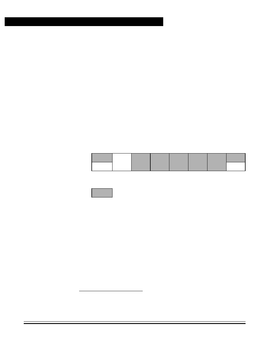
Advance Information
MC68HC705JJ7 ∑ MC68HC705JP7 -- REV 4
188
EPROM/OTPROM
MOTOROLA
EPROM/OTPROM
COPEN -- COP Watchdog Enable Bit
This EPROM bit enables the COP watchdog.
1 = COP watchdog enabled
0 = COP watchdog disabled
13.3.3 EPROM Security Bit
An EPROM programmable bit is provided at the location of the COP
watchdog register at $1FF0 as shown in
Figure 13-3
. This bit allows
control of access to the EPROM array. Any accesses of the EPROM
locations will return undefined results when the EPMSEC bit is set. Refer
to
13.4.2 EPMSEC Programming
for programming instructions.
EPMSEC -- EPROM Security
1
This EPROM write-only bit enables the access to the EPROM array.
1 = Access to the EPROM array in non-user modes is denied.
0 = Access to the EPROM array in non-user modes is enabled.
Address:
$1FF0
Bit 7
6
5
4
3
2
1
Bit 0
Read:
OPT
Write:
EPMSEC
COPC
Reset:
Unaffected by reset
Erased:
0
--
--
--
--
--
--
--
= Unimplemented
Figure 13-3. EPROM Security in COP and Security Register (COPR)
1. No security feature is absolutely secure. However, Motorola's strategy is to make reading or
copying the EPROM/OTPROM difficult for unauthorized users.

EPROM/OTPROM
EPROM Programming
MC68HC705JJ7 ∑ MC68HC705JP7 -- REV 4
Advance Information
MOTOROLA
EPROM/OTPROM
189
13.4 EPROM Programming
A programming board is available from Motorola to download to the
on-chip EPROM/OTPROM using the factory-provided programming
software. Factory-provided software for programming the PEPROM is
available on the World Wide Web at:
http://www.motorola.com/mcu/
The programming software copies to the 6144-byte space located at
EPROM addresses $0700≠$1EFF and to the 16-byte space at
addresses $1FF0≠$1FFF which includes the mask option register at
address $1FF1, and the security bit at address $1FF0.
NOTE:
To program the EPROM/OTPROM, MOR, or EPMSEC bits properly, the
V
DD
voltage must be greater than 4.5 volts.
13.4.1 MOR Programming
The contents of the MOR should be programmed using the programmer
board. To program any bits in the MOR, the desired bit states must be
written to the MOR address and then the MPGM bit in the EPROG
register must be used. The following sequence will program the MOR:
1. Write the desired data to the MOR location ($1FF1).
2. Apply the programming voltage to the IRQ/V
PP
pin.
3. Set the MPGM bit in the EPROG.
4. Wait for the programming time, t
MPGM
.
5. Clear the MPGM bit in the EPROG.
6. Remove the programming voltage from the IRQ/V
PP
pin.
Once the MOR bits have been programmed, some of the options may
experience glitches in operation after removal of the programming
voltage. It is recommended that the part be reset before trying to verify
the contents of the user EPROM or the MOR itself.
NOTE:
The contents of the EPROM or the MOR cannot be accessed if the
EPMSEC bit in the COPR register has been set.

Advance Information
MC68HC705JJ7 ∑ MC68HC705JP7 -- REV 4
190
EPROM/OTPROM
MOTOROLA
EPROM/OTPROM
13.4.2 EPMSEC Programming
The EPMSEC bit is programmable. To program the EPMSEC bit, the
desired state must be written to the COP address and then the MPGM
bit in the EPROG register must be used. The following sequence will
program the EPMSEC bit:
1. Write the desired data to bit 7 of the COPR location ($1FF0).
2. Apply the programming voltage to the IRQ/V
PP
pin.
3. Set the MPGM bit in the EPROG.
4. Wait for the programming time, t
MPGM
.
5. Clear the MPGM bit in the EPROG.
6. Remove the programming voltage from the IRQ/V
PP
pin.
Once the EPMSEC bit has been programmed to a logic 1, access to the
contents of the EPROM and MOR in the expanded non-user modes will
be denied. It is therefore recommended that the user EPROM and MOR
in the part first be programmed and fully verified before setting the
EPMSEC bit.
13.5 EPROM Erasing
MCUs with windowed packages permit EPROM erasing with ultraviolet
light. Erase the EPROM by exposing it to 15 Ws/cm
2
of ultraviolet light
with a wavelength of 2537 angstroms. Position the ultraviolet light
source 1 inch from the window. Do not use a shortwave filter. The erased
state of an EPROM bit is a logic 0.
NOTE:
Unlike many commercial EPROMs, an erased EPROM byte in the MCU
will read as $00. All unused locations should be programmed as 0s.

MC68HC705JJ7 ∑ MC68HC705JP7 -- REV 4
Advance Information
MOTOROLA
Instruction Set
191
Advance Information -- MC68HC705JJ7/MC68HC705JP7
Section 14. Instruction Set
14.1 Contents
14.2
Introduction . . . . . . . . . . . . . . . . . . . . . . . . . . . . . . . . . . . . . . . 191
14.3
Addressing Modes . . . . . . . . . . . . . . . . . . . . . . . . . . . . . . . . .192
14.3.1
Inherent . . . . . . . . . . . . . . . . . . . . . . . . . . . . . . . . . . . . . . . 192
14.3.2
Immediate. . . . . . . . . . . . . . . . . . . . . . . . . . . . . . . . . . . . . . 192
14.3.3
Direct . . . . . . . . . . . . . . . . . . . . . . . . . . . . . . . . . . . . . . . . . 193
14.3.4
Extended . . . . . . . . . . . . . . . . . . . . . . . . . . . . . . . . . . . . . . 193
14.3.5
Indexed, No Offset . . . . . . . . . . . . . . . . . . . . . . . . . . . . . . . 193
14.3.6
Indexed, 8-Bit Offset. . . . . . . . . . . . . . . . . . . . . . . . . . . . . . 193
14.3.7
Indexed, 16-Bit Offset. . . . . . . . . . . . . . . . . . . . . . . . . . . . .194
14.3.8
Relative . . . . . . . . . . . . . . . . . . . . . . . . . . . . . . . . . . . . . . . 194
14.4
Instruction Types . . . . . . . . . . . . . . . . . . . . . . . . . . . . . . . . . . 195
14.4.1
Register/Memory Instructions. . . . . . . . . . . . . . . . . . . . . . . 195
14.4.2
Read-Modify-Write Instructions . . . . . . . . . . . . . . . . . . . . . 196
14.4.3
Jump/Branch Instructions. . . . . . . . . . . . . . . . . . . . . . . . . . 197
14.4.4
Bit Manipulation Instructions . . . . . . . . . . . . . . . . . . . . . . . 199
14.4.5
Control Instructions . . . . . . . . . . . . . . . . . . . . . . . . . . . . . . 200
14.5
Instruction Set Summary . . . . . . . . . . . . . . . . . . . . . . . . . . . . 201
14.6
Opcode Map . . . . . . . . . . . . . . . . . . . . . . . . . . . . . . . . . . . . . . 207
14.2 Introduction
The microcontroller unit (MCU) instruction set has 62 instructions and
uses eight addressing modes. The instructions include all those of the
M146805 CMOS Family plus one more: the unsigned multiply (MUL)
instruction. The MUL instruction allows unsigned multiplication of the
contents of the accumulator (A) and the index register (X). The

Advance Information
MC68HC705JJ7 ∑ MC68HC705JP7 -- REV 4
192
Instruction Set
MOTOROLA
Instruction Set
high-order product is stored in the index register, and the low-order
product is stored in the accumulator.
14.3 Addressing Modes
The CPU uses eight addressing modes for flexibility in accessing data.
The addressing modes provide eight different ways for the CPU to find
the data required to execute an instruction. The eight addressing modes
are:
∑
Inherent
∑
Immediate
∑
Direct
∑
Extended
∑
Indexed, no offset
∑
Indexed, 8-bit offset
∑
Indexed, 16-bit offset
∑
Relative
14.3.1 Inherent
Inherent instructions are those that have no operand, such as return
from interrupt (RTI) and stop (STOP). Some of the inherent instructions
act on data in the CPU registers, such as set carry flag (SEC) and
increment accumulator (INCA). Inherent instructions require no operand
address and are one byte long.
14.3.2 Immediate
Immediate instructions are those that contain a value to be used in an
operation with the value in the accumulator or index register. Immediate
instructions require no operand address and are two bytes long. The
opcode is the first byte, and the immediate data value is the second byte.

Instruction Set
Addressing Modes
MC68HC705JJ7 ∑ MC68HC705JP7 -- REV 4
Advance Information
MOTOROLA
Instruction Set
193
14.3.3 Direct
Direct instructions can access any of the first 256 memory locations with
two bytes. The first byte is the opcode, and the second is the low byte of
the operand address. In direct addressing, the CPU automatically uses
$00 as the high byte of the operand address.
14.3.4 Extended
Extended instructions use three bytes and can access any address in
memory. The first byte is the opcode; the second and third bytes are the
high and low bytes of the operand address.
When using the Motorola assembler, the programmer does not need to
specify whether an instruction is direct or extended. The assembler
automatically selects the shortest form of the instruction.
14.3.5 Indexed, No Offset
Indexed instructions with no offset are 1-byte instructions that can
access data with variable addresses within the first 256 memory
locations. The index register contains the low byte of the effective
address of the operand. The CPU automatically uses $00 as the high
byte, so these instructions can address locations $0000≠$00FF.
Indexed, no offset instructions are often used to move a pointer through
a table or to hold the address of a frequently used random-access
memory (RAM) or input/output (I/O) location.
14.3.6 Indexed, 8-Bit Offset
Indexed, 8-bit offset instructions are 2-byte instructions that can access
data with variable addresses within the first 511 memory locations. The
CPU adds the unsigned byte in the index register to the unsigned byte
following the opcode. The sum is the effective address of the operand.
These instructions can access locations $0000≠$01FE.

Advance Information
MC68HC705JJ7 ∑ MC68HC705JP7 -- REV 4
194
Instruction Set
MOTOROLA
Instruction Set
Indexed 8-bit offset instructions are useful for selecting the kth element
in an n-element table. The table can begin anywhere within the first 256
memory locations and could extend as far as location 510 ($01FE). The
k value is typically in the index register, and the address of the beginning
of the table is in the byte following the opcode.
14.3.7 Indexed, 16-Bit Offset
Indexed, 16-bit offset instructions are 3-byte instructions that can access
data with variable addresses at any location in memory. The CPU adds
the unsigned byte in the index register to the two unsigned bytes
following the opcode. The sum is the effective address of the operand.
The first byte after the opcode is the high byte of the 16-bit offset; the
second byte is the low byte of the offset.
Indexed, 16-bit offset instructions are useful for selecting the kth element
in an n-element table anywhere in memory.
As with direct and extended addressing, the Motorola assembler
determines the shortest form of indexed addressing.
14.3.8 Relative
Relative addressing is only for branch instructions. If the branch
condition is true, the CPU finds the effective branch destination by
adding the signed byte following the opcode to the contents of the
program counter. If the branch condition is not true, the CPU goes to the
next instruction. The offset is a signed, two's complement byte that gives
a branching range of ≠128 to +127 bytes from the address of the next
location after the branch instruction.
When using the Motorola assembler, the programmer does not need to
calculate the offset, because the assembler determines the proper offset
and verifies that it is within the span of the branch.

Instruction Set
Instruction Types
MC68HC705JJ7 ∑ MC68HC705JP7 -- REV 4
Advance Information
MOTOROLA
Instruction Set
195
14.4 Instruction Types
The MCU instructions fall into the following five categories:
∑
Register/memory instructions
∑
Read-modify-write instructions
∑
Jump/branch instructions
∑
Bit manipulation instructions
∑
Control instructions
14.4.1 Register/Memory Instructions
These instructions operate on CPU registers and memory locations.
Most of them use two operands. One operand is in either the
accumulator or the index register. The CPU finds the other operand in
memory.
Table 14-1. Register/Memory Instructions
Instruction
Mnemonic
Add Memory Byte and Carry Bit to Accumulator
ADC
Add Memory Byte to Accumulator
ADD
AND Memory Byte with Accumulator
AND
Bit Test Accumulator
BIT
Compare Accumulator
CMP
Compare Index Register with Memory Byte
CPX
EXCLUSIVE OR Accumulator with Memory Byte
EOR
Load Accumulator with Memory Byte
LDA
Load Index Register with Memory Byte
LDX
Multiply
MUL
OR Accumulator with Memory Byte
ORA
Subtract Memory Byte and Carry Bit from Accumulator
SBC
Store Accumulator in Memory
STA
Store Index Register in Memory
STX
Subtract Memory Byte from Accumulator
SUB

Advance Information
MC68HC705JJ7 ∑ MC68HC705JP7 -- REV 4
196
Instruction Set
MOTOROLA
Instruction Set
14.4.2 Read-Modify-Write Instructions
These instructions read a memory location or a register, modify its
contents, and write the modified value back to the memory location or to
the register.
NOTE:
Do not use read-modify-write operations on write-only registers.
Table 14-2. Read-Modify-Write Instructions
Instruction
Mnemonic
Arithmetic Shift Left (Same as LSL)
ASL
Arithmetic Shift Right
ASR
Bit Clear
BCLR
(1)
1. Unlike other read-modify-write instructions, BCLR and
BSET use only direct addressing.
Bit Set
BSET
(1)
Clear Register
CLR
Complement (One's Complement)
COM
Decrement
DEC
Increment
INC
Logical Shift Left (Same as ASL)
LSL
Logical Shift Right
LSR
Negate (Two's Complement)
NEG
Rotate Left through Carry Bit
ROL
Rotate Right through Carry Bit
ROR
Test for Negative or Zero
TST
(2)
2. TST is an exception to the read-modify-write sequence be-
cause it does not write a replacement value.

Instruction Set
Instruction Types
MC68HC705JJ7 ∑ MC68HC705JP7 -- REV 4
Advance Information
MOTOROLA
Instruction Set
197
14.4.3 Jump/Branch Instructions
Jump instructions allow the CPU to interrupt the normal sequence of the
program counter. The unconditional jump instruction (JMP) and the
jump-to-subroutine instruction (JSR) have no register operand. Branch
instructions allow the CPU to interrupt the normal sequence of the
program counter when a test condition is met. If the test condition is not
met, the branch is not performed.
The BRCLR and BRSET instructions cause a branch based on the state
of any readable bit in the first 256 memory locations. These 3-byte
instructions use a combination of direct addressing and relative
addressing. The direct address of the byte to be tested is in the byte
following the opcode. The third byte is the signed offset byte. The CPU
finds the effective branch destination by adding the third byte to the
program counter if the specified bit tests true. The bit to be tested and its
condition (set or clear) is part of the opcode. The span of branching is
from ≠128 to +127 from the address of the next location after the branch
instruction. The CPU also transfers the tested bit to the carry/borrow bit
of the condition code register.
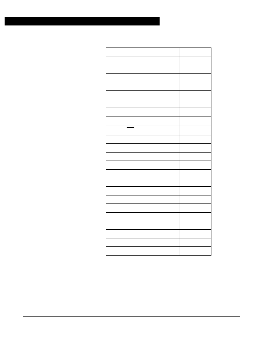
Advance Information
MC68HC705JJ7 ∑ MC68HC705JP7 -- REV 4
198
Instruction Set
MOTOROLA
Instruction Set
Table 14-3. Jump and Branch Instructions
Instruction
Mnemonic
Branch if Carry Bit Clear
BCC
Branch if Carry Bit Set
BCS
Branch if Equal
BEQ
Branch if Half-Carry Bit Clear
BHCC
Branch if Half-Carry Bit Set
BHCS
Branch if Higher
BHI
Branch if Higher or Same
BHS
Branch if IRQ/V
PP
Pin High
BIH
Branch if IRQ/V
PP
Pin Low
BIL
Branch if Lower
BLO
Branch if Lower or Same
BLS
Branch if Interrupt Mask Clear
BMC
Branch if Minus
BMI
Branch if Interrupt Mask Set
BMS
Branch if Not Equal
BNE
Branch if Plus
BPL
Branch Always
BRA
Branch if Bit Clear
BRCLR
Branch Never
BRN
Branch if Bit Set
BRSET
Branch to Subroutine
BSR
Unconditional Jump
JMP
Jump to Subroutine
JSR

Instruction Set
Instruction Types
MC68HC705JJ7 ∑ MC68HC705JP7 -- REV 4
Advance Information
MOTOROLA
Instruction Set
199
14.4.4 Bit Manipulation Instructions
The CPU can set or clear any writable bit in the first 256 bytes of
memory, which includes I/O registers and on-chip RAM locations. The
CPU can also test and branch based on the state of any bit in any of the
first 256 memory locations.
Table 14-4. Bit Manipulation Instructions
Instruction
Mnemonic
Bit Clear
BCLR
Branch if Bit Clear
BRCLR
Branch if Bit Set
BRSET
Bit Set
BSET
Advance Information
MC68HC705JJ7 ∑ MC68HC705JP7 -- REV 4
200
Instruction Set
MOTOROLA
Instruction Set
14.4.5 Control Instructions
These instructions act on central processor unit (CPU) registers and
control CPU operation during program execution.
Table 14-5. Control Instructions
Instruction
Mnemonic
Clear Carry Bit
CLC
Clear Interrupt Mask
CLI
No Operation
NOP
Reset Stack Pointer
RSP
Return from Interrupt
RTI
Return from Subroutine
RTS
Set Carry Bit
SEC
Set Interrupt Mask
SEI
Stop Oscillator and Enable IRQ/V
PP
Pin
STOP
Software Interrupt
SWI
Transfer Accumulator to Index Register
TAX
Transfer Index Register to Accumulator
TXA
Stop CPU Clock and Enable Interrupts
WAIT
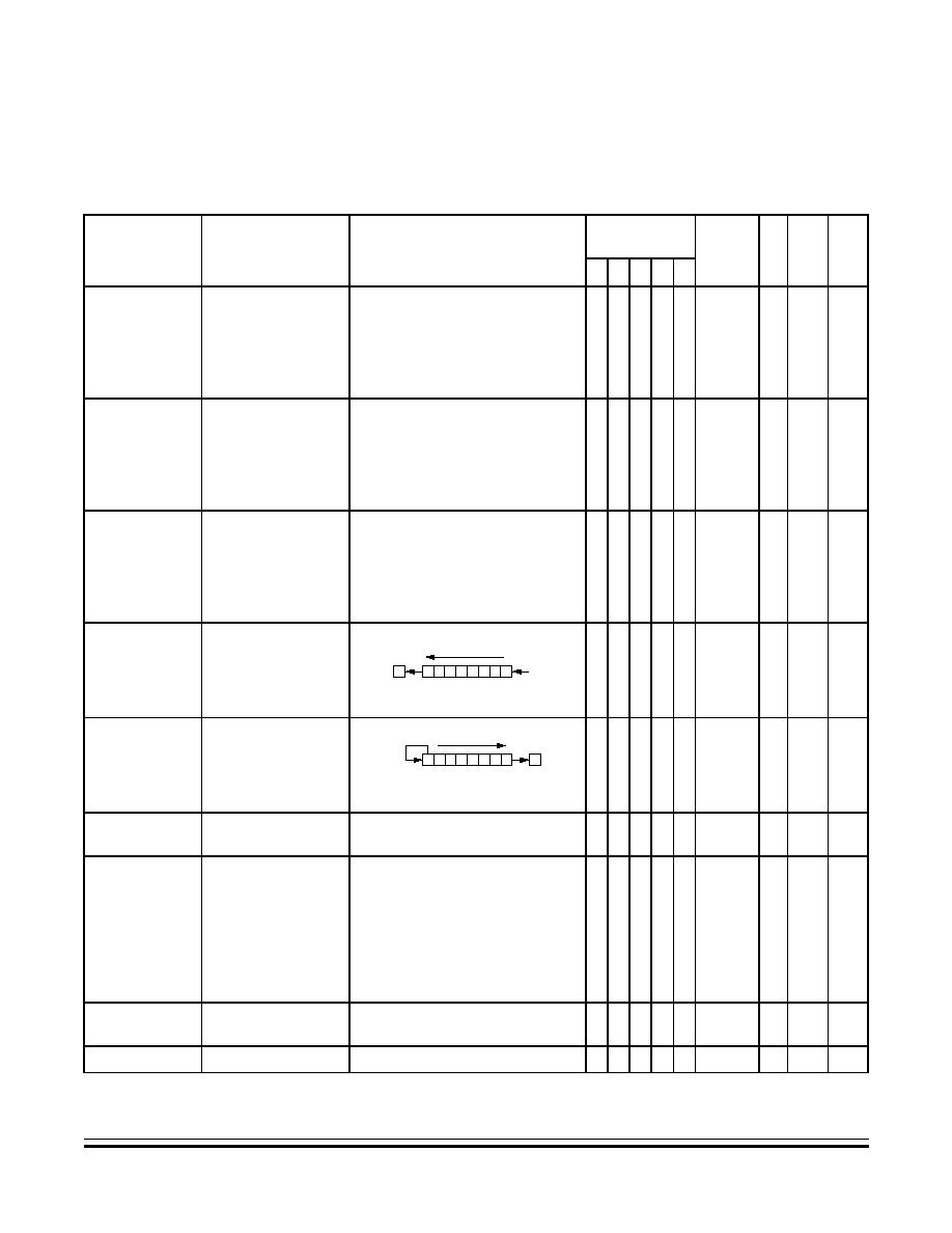
Instruction Set
Instruction Set Summary
MC68HC705JJ7 ∑ MC68HC705JP7 -- REV 4
Advance Information
MOTOROLA
Instruction Set
201
14.5 Instruction Set Summary
.
Table 14-6. Instruction Set Summary (Sheet 1 of 7)
Source
Form
Operation
Description
Effect
on CCR
Addr
e
s
s
M
ode
Opc
ode
O
p
er
an
d
Cy
cles
H I N Z C
ADC #opr
ADC opr
ADC opr
ADC opr,X
ADC opr,X
ADC ,X
Add with Carry
A
(A) + (M) + (C)
--
IMM
DIR
EXT
IX2
IX1
IX
A9
B9
C9
D9
E9
F9
ii
dd
hh ll
ee ff
ff
2
3
4
5
4
3
ADD #opr
ADD opr
ADD opr
ADD opr,X
ADD opr,X
ADD ,X
Add without Carry
A
(A) + (M)
--
IMM
DIR
EXT
IX2
IX1
IX
AB
BB
CB
DB
EB
FB
ii
dd
hh ll
ee ff
ff
2
3
4
5
4
3
AND #opr
AND opr
AND opr
AND opr,X
AND opr,X
AND ,X
Logical AND
A
(A)
(M)
-- --
--
IMM
DIR
EXT
IX2
IX1
IX
A4
B4
C4
D4
E4
F4
ii
dd
hh ll
ee ff
ff
2
3
4
5
4
3
ASL opr
ASLA
ASLX
ASL opr,X
ASL ,X
Arithmetic Shift Left
(Same as LSL)
-- --
DIR
INH
INH
IX1
IX
38
48
58
68
78
dd
ff
5
3
3
6
5
ASR opr
ASRA
ASRX
ASR opr,X
ASR ,X
Arithmetic Shift Right
-- --
DIR
INH
INH
IX1
IX
37
47
57
67
77
dd
ff
5
3
3
6
5
BCC rel
Branch if Carry Bit
Clear
PC
(PC) + 2 + rel ? C = 0
-- -- -- -- --
REL
24
rr
3
BCLR n opr
Clear Bit n
Mn
0
-- -- -- -- --
DIR (b0)
DIR (b1)
DIR (b2)
DIR (b3)
DIR (b4)
DIR (b5)
DIR (b6)
DIR (b7)
11
13
15
17
19
1B
1D
1F
dd
dd
dd
dd
dd
dd
dd
dd
5
5
5
5
5
5
5
5
BCS rel
Branch if Carry Bit Set
(Same as BLO)
PC
(PC) + 2 + rel ? C = 1
-- -- -- -- --
REL
25
rr
3
BEQ rel
Branch if Equal
PC
(PC) + 2 + rel ? Z = 1
-- -- -- -- --
REL
27
rr
3
C
b0
b7
0
b0
b7
C
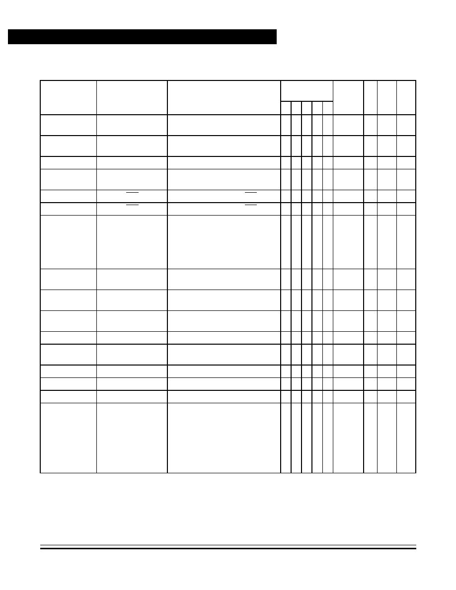
Advance Information
MC68HC705JJ7 ∑ MC68HC705JP7 -- REV 4
202
Instruction Set
MOTOROLA
Instruction Set
BHCC rel
Branch if Half-Carry
Bit Clear
PC
(PC) + 2 + rel ? H = 0
-- -- -- -- --
REL
28
rr
3
BHCS rel
Branch if Half-Carry
Bit Set
PC
(PC) + 2 + rel ? H = 1
-- -- -- -- --
REL
29
rr
3
BHI rel
Branch if Higher
PC
(PC) + 2 + rel ? C
Z = 0
-- -- -- -- --
REL
22
rr
3
BHS rel
Branch if Higher or
Same
PC
(PC) + 2 + rel ? C = 0
-- -- -- -- --
REL
24
rr
3
BIH rel
Branch if IRQ Pin High
PC
(PC) + 2 + rel ? IRQ = 1
-- -- -- -- --
REL
2F
rr
3
BIL rel
Branch if IRQ Pin Low
PC
(PC) + 2 + rel ? IRQ = 0
-- -- -- -- --
REL
2E
rr
3
BIT #opr
BIT opr
BIT opr
BIT opr,X
BIT opr,X
BIT ,X
Bit Test
Accumulator with
Memory Byte
(A)
(M)
-- --
--
IMM
DIR
EXT
IX2
IX1
IX
A5
B5
C5
D5
E5
F5
ii
dd
hh ll
ee ff
ff
p
2
3
4
5
4
3
BLO rel
Branch if Lower
(Same as BCS)
PC
(PC) + 2 + rel ? C = 1
-- -- -- -- --
REL
25
rr
3
BLS rel
Branch if Lower or
Same
PC
(PC) + 2 + rel ? C
Z = 1
-- -- -- -- --
REL
23
rr
3
BMC rel
Branch if Interrupt
Mask Clear
PC
(PC) + 2 + rel ? I = 0
-- -- -- -- --
REL
2C
rr
3
BMI rel
Branch if Minus
PC
(PC) + 2 + rel ? N = 1
-- -- -- -- --
REL
2B
rr
3
BMS rel
Branch if Interrupt
Mask Set
PC
(PC) + 2 + rel ? I = 1
-- -- -- -- --
REL
2D
rr
3
BNE rel
Branch if Not Equal
PC
(PC) + 2 + rel ? Z = 0
-- -- -- -- --
REL
26
rr
3
BPL rel
Branch if Plus
PC
(PC) + 2 + rel ? N = 0
-- -- -- -- --
REL
2A
rr
3
BRA rel
Branch Always
PC
(PC) + 2 + rel ? 1 = 1
-- -- -- -- --
REL
20
rr
3
BRCLR n opr rel
Branch if bit n clear
PC
(PC) + 2 + rel ? Mn = 0
-- -- -- --
DIR (b0)
DIR (b1)
DIR (b2)
DIR (b3)
DIR (b4)
DIR (b5)
DIR (b6)
DIR (b7)
01
03
05
07
09
0B
0D
0F
dd rr
dd rr
dd rr
dd rr
dd rr
dd rr
dd rr
dd rr
5
5
5
5
5
5
5
5
Table 14-6. Instruction Set Summary (Sheet 2 of 7)
Source
Form
Operation
Description
Effect
on CCR
Addr
e
s
s
M
ode
Opc
ode
O
p
er
an
d
Cy
cles
H I N Z C
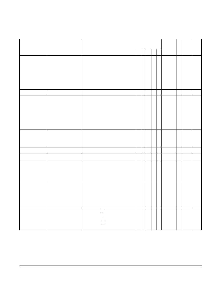
Instruction Set
Instruction Set Summary
MC68HC705JJ7 ∑ MC68HC705JP7 -- REV 4
Advance Information
MOTOROLA
Instruction Set
203
BRSET n opr rel
Branch if Bit n Set
PC
(PC) + 2 + rel ? Mn = 1
-- -- -- --
DIR (b0)
DIR (b1)
DIR (b2)
DIR (b3)
DIR (b4)
DIR (b5)
DIR (b6)
DIR (b7)
00
02
04
06
08
0A
0C
0E
dd rr
dd rr
dd rr
dd rr
dd rr
dd rr
dd rr
dd rr
5
5
5
5
5
5
5
5
BRN rel
Branch Never
PC
(PC) + 2 + rel ? 1 = 0
-- -- -- -- --
REL
21
rr
3
BSET n opr
Set Bit n
Mn
1
-- -- -- -- --
DIR (b0)
DIR (b1)
DIR (b2)
DIR (b3)
DIR (b4)
DIR (b5)
DIR (b6)
DIR (b7)
10
12
14
16
18
1A
1C
1E
dd
dd
dd
dd
dd
dd
dd
dd
5
5
5
5
5
5
5
5
BSR rel
Branch to
Subroutine
PC
(PC) + 2; push (PCL)
SP
(SP) ≠ 1; push (PCH)
SP
(SP) ≠ 1
PC
(PC) + rel
-- -- -- -- --
REL
AD
rr
6
CLC
Clear Carry Bit
C
0
-- -- -- -- 0
INH
98
2
CLI
Clear Interrupt Mask
I
0
-- 0 -- -- --
INH
9A
2
CLR opr
CLRA
CLRX
CLR opr,X
CLR ,X
Clear Byte
M
$00
A
$00
X
$00
M
$00
M
$00
-- -- 0
1 --
DIR
INH
INH
IX1
IX
3F
4F
5F
6F
7F
dd
ff
5
3
3
6
5
CMP #opr
CMP opr
CMP opr
CMP opr,X
CMP opr,X
CMP ,X
Compare
Accumulator with
Memory Byte
(A) ≠ (M)
-- --
IMM
DIR
EXT
IX2
IX1
IX
A1
B1
C1
D1
E1
F1
ii
dd
hh ll
ee ff
ff
2
3
4
5
4
3
COM opr
COMA
COMX
COM opr,X
COM ,X
Complement Byte
(One's Complement)
M
( ) = $FF ≠ (M)
A
( ) = $FF ≠ (M)
X
( ) = $FF ≠ (M)
M
( ) = $FF ≠ (M)
M
( ) = $FF ≠ (M)
-- --
1
DIR
INH
INH
IX1
IX
33
43
53
63
73
dd
ff
5
3
3
6
5
Table 14-6. Instruction Set Summary (Sheet 3 of 7)
Source
Form
Operation
Description
Effect
on CCR
Addr
e
s
s
M
ode
Opc
ode
O
p
er
an
d
Cy
cles
H I N Z C
M
A
X
M
M

Advance Information
MC68HC705JJ7 ∑ MC68HC705JP7 -- REV 4
204
Instruction Set
MOTOROLA
Instruction Set
CPX #opr
CPX opr
CPX opr
CPX opr,X
CPX opr,X
CPX ,X
Compare Index
Register with
Memory Byte
(X) ≠ (M)
-- --
1
IMM
DIR
EXT
IX2
IX1
IX
A3
B3
C3
D3
E3
F3
ii
dd
hh ll
ee ff
ff
2
3
4
5
4
3
DEC opr
DECA
DECX
DEC opr,X
DEC ,X
Decrement Byte
M
(M) ≠ 1
A
(A) ≠ 1
X
(X) ≠ 1
M
(M) ≠ 1
M
(M) ≠ 1
-- --
--
DIR
INH
INH
IX1
IX
3A
4A
5A
6A
7A
dd
ff
5
3
3
6
5
EOR #opr
EOR opr
EOR opr
EOR opr,X
EOR opr,X
EOR ,X
EXCLUSIVE OR
Accumulator with
Memory Byte
A
(A)
(M)
-- --
--
IMM
DIR
EXT
IX2
IX1
IX
A8
B8
C8
D8
E8
F8
ii
dd
hh ll
ee ff
ff
2
3
4
5
4
3
INC opr
INCA
INCX
INC opr,X
INC ,X
Increment Byte
M
(M) + 1
A
(A) + 1
X
(X) + 1
M
(M) + 1
M
(M) + 1
-- --
--
DIR
INH
INH
IX1
IX
3C
4C
5C
6C
7C
dd
ff
5
3
3
6
5
JMP opr
JMP opr
JMP opr,X
JMP opr,X
JMP ,X
Unconditional Jump
PC
Jump Address
-- -- -- -- --
DIR
EXT
IX2
IX1
IX
BC
CC
DC
EC
FC
dd
hh ll
ee ff
ff
2
3
4
3
2
JSR opr
JSR opr
JSR opr,X
JSR opr,X
JSR ,X
Jump to Subroutine
PC
(PC) + n (n = 1, 2, or 3)
Push (PCL); SP
(SP) ≠ 1
Push (PCH); SP
(SP) ≠ 1
PC
Conditional Address
-- -- -- -- --
DIR
EXT
IX2
IX1
IX
BD
CD
DD
ED
FD
dd
hh ll
ee ff
ff
5
6
7
6
5
LDA #opr
LDA opr
LDA opr
LDA opr,X
LDA opr,X
LDA ,X
Load Accumulator with
Memory Byte
A
(M)
-- --
--
IMM
DIR
EXT
IX2
IX1
IX
A6
B6
C6
D6
E6
F6
ii
dd
hh ll
ee ff
ff
2
3
4
5
4
3
Table 14-6. Instruction Set Summary (Sheet 4 of 7)
Source
Form
Operation
Description
Effect
on CCR
Addr
e
s
s
M
ode
Opc
ode
O
p
er
an
d
Cy
cles
H I N Z C
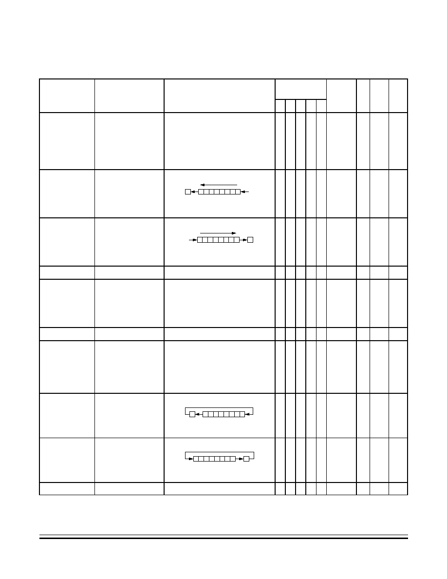
Instruction Set
Instruction Set Summary
MC68HC705JJ7 ∑ MC68HC705JP7 -- REV 4
Advance Information
MOTOROLA
Instruction Set
205
LDX #opr
LDX opr
LDX opr
LDX opr,X
LDX opr,X
LDX ,X
Load Index Register
with Memory Byte
X
(M)
-- --
--
IMM
DIR
EXT
IX2
IX1
IX
AE
BE
CE
DE
EE
FE
ii
dd
hh ll
ee ff
ff
2
3
4
5
4
3
LSL opr
LSLA
LSLX
LSL opr,X
LSL ,X
Logical Shift Left
(Same as ASL)
-- --
DIR
INH
INH
IX1
IX
38
48
58
68
78
dd
ff
5
3
3
6
5
LSR opr
LSRA
LSRX
LSR opr,X
LSR ,X
Logical Shift Right
-- -- 0
DIR
INH
INH
IX1
IX
34
44
54
64
74
dd
ff
5
3
3
6
5
MUL
Unsigned Multiply
X : A
(X)
◊
(A)
0 -- -- -- 0
INH
42
11
NEG opr
NEGA
NEGX
NEG opr,X
NEG ,X
Negate Byte
(Two's Complement)
M
≠(M) = $00 ≠ (M)
A
≠(A) = $00 ≠ (A)
X
≠(X) = $00 ≠ (X)
M
≠(M) = $00 ≠ (M)
M
≠(M) = $00 ≠ (M)
-- --
DIR
INH
INH
IX1
IX
30
40
50
60
70
ii
ff
5
3
3
6
5
NOP
No Operation
-- -- -- -- --
INH
9D
2
ORA #opr
ORA opr
ORA opr
ORA opr,X
ORA opr,X
ORA ,X
Logical OR
Accumulator with
Memory
A
(A)
(M)
-- --
--
IMM
DIR
EXT
IX2
IX1
IX
AA
BA
CA
DA
EA
FA
ii
dd
hh ll
ee ff
ff
2
3
4
5
4
3
ROL opr
ROLA
ROLX
ROL opr,X
ROL ,X
Rotate Byte Left
through Carry Bit
-- --
DIR
INH
INH
IX1
IX
39
49
59
69
79
dd
ff
5
3
3
6
5
ROR opr
RORA
RORX
ROR opr,X
ROR ,X
Rotate Byte Right
through Carry Bit
-- --
DIR
INH
INH
IX1
IX
36
46
56
66
76
dd
ff
5
3
3
6
5
RSP
Reset Stack Pointer
SP
$00FF
-- -- -- -- --
INH
9C
2
Table 14-6. Instruction Set Summary (Sheet 5 of 7)
Source
Form
Operation
Description
Effect
on CCR
Addr
e
s
s
M
ode
Opc
ode
O
p
er
an
d
Cy
cles
H I N Z C
C
b0
b7
0
b0
b7
C
0
C
b0
b7
b0
b7
C
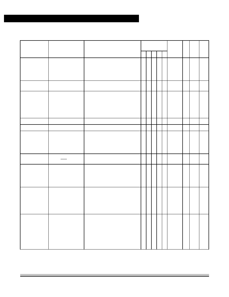
Advance Information
MC68HC705JJ7 ∑ MC68HC705JP7 -- REV 4
206
Instruction Set
MOTOROLA
Instruction Set
RTI
Return from Interrupt
SP
(SP) + 1; Pull (CCR)
SP
(SP) + 1; Pull (A)
SP
(SP) + 1; Pull (X)
SP
(SP) + 1; Pull (PCH)
SP
(SP) + 1; Pull (PCL)
INH
80
6
RTS
Return from
Subroutine
SP
(SP) + 1; Pull (PCH)
SP
(SP) + 1; Pull (PCL)
INH
SBC #opr
SBC opr
SBC opr
SBC opr,X
SBC opr,X
SBC ,X
Subtract Memory Byte
and Carry Bit from
Accumulator
A
(A) ≠ (M) ≠ (C)
-- --
IMM
DIR
EXT
IX2
IX1
IX
A2
B2
C2
D2
E2
F2
ii
dd
hh ll
ee ff
ff
2
3
4
5
4
3
SEC
Set Carry Bit
C
1
-- -- -- -- 1
INH
99
2
SEI
Set Interrupt Mask
I
1
-- 1 -- -- --
INH
9B
2
STA opr
STA opr
STA opr,X
STA opr,X
STA ,X
Store Accumulator in
Memory
M
(A)
-- --
--
DIR
EXT
IX2
IX1
IX
B7
C7
D7
E7
F7
dd
hh ll
ee ff
ff
4
5
6
5
4
STOP
Stop Oscillator and
Enable IRQ Pin
-- 0 -- -- --
INH
8E
2
STX opr
STX opr
STX opr,X
STX opr,X
STX ,X
Store Index
Register In Memory
M
(X)
-- --
--
DIR
EXT
IX2
IX1
IX
BF
CF
DF
EF
FF
dd
hh ll
ee ff
ff
4
5
6
5
4
SUB #opr
SUB opr
SUB opr
SUB opr,X
SUB opr,X
SUB ,X
Subtract Memory Byte
from
Accumulator
A
(A) ≠ (M)
-- --
IMM
DIR
EXT
IX2
IX1
IX
A0
B0
C0
D0
E0
F0
ii
dd
hh ll
ee ff
ff
2
3
4
5
4
3
SWI
Software Interrupt
PC
(PC) + 1; Push (PCL)
SP
(SP) ≠ 1; Push (PCH)
SP
(SP) ≠ 1; Push (X)
SP
(SP) ≠ 1; Push (A)
SP
(SP) ≠ 1; Push (CCR)
SP
(SP) ≠ 1; I
1
PCH
Interrupt Vector High Byte
PCL
Interrupt Vector Low Byte
-- 1 -- -- --
INH
83
10
Table 14-6. Instruction Set Summary (Sheet 6 of 7)
Source
Form
Operation
Description
Effect
on CCR
Addr
e
s
s
M
ode
Opc
ode
O
p
er
an
d
Cy
cles
H I N Z C
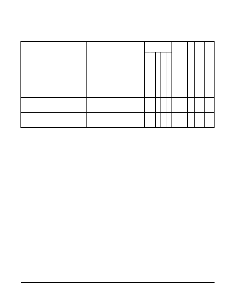
Instruction Set
Opcode Map
MC68HC705JJ7 ∑ MC68HC705JP7 -- REV 4
Advance Information
MOTOROLA
Instruction Set
207
14.6 Opcode Map
See
Table 14-7
.
TAX
Transfer
Accumulator to Index
Register
X
(A)
-- -- -- -- --
INH
97
2
TST opr
TSTA
TSTX
TST opr,X
TST ,X
Test Memory Byte for
Negative or Zero
(M) ≠ $00
-- -- -- -- --
DIR
INH
INH
IX1
IX
3D
4D
5D
6D
7D
dd
ff
4
3
3
5
4
TXA
Transfer Index
Register to
Accumulator
A
(X)
-- -- -- -- --
INH
9F
2
WAIT
Stop CPU Clock and
Enable
Interrupts
--
-- -- --
INH
8F
2
A
Accumulator
opr
Operand (one or two bytes)
C
Carry/borrow flag
PC
Program counter
CCR Condition code register
PCH Program counter high byte
dd
Direct address of operand
PCL
Program counter low byte
dd rr
Direct address of operand and relative offset of branch instruction
REL
Relative addressing mode
DIR
Direct addressing mode
rel
Relative program counter offset byte
ee ff
High and low bytes of offset in indexed, 16-bit offset addressing
rr
Relative program counter offset byte
EXT
Extended addressing mode
SP
Stack pointer
ff
Offset byte in indexed, 8-bit offset addressing
X
Index register
H
Half-carry flag
Z
Zero flag
hh ll
High and low bytes of operand address in extended addressing
#
Immediate value
I
Interrupt mask
Logical AND
ii
Immediate operand byte
Logical OR
IMM
Immediate addressing mode
Logical EXCLUSIVE OR
INH
Inherent addressing mode
( )
Contents of
IX
Indexed, no offset addressing mode
≠( )
Negation (two's complement)
IX1
Indexed, 8-bit offset addressing mode
Loaded with
IX2
Indexed, 16-bit offset addressing mode
?
If
M
Memory location
:
Concatenated with
N
Negative flag
Set or cleared
n
Any bit
--
Not affected
Table 14-6. Instruction Set Summary (Sheet 7 of 7)
Source
Form
Operation
Description
Effect
on CCR
Addr
e
s
s
M
ode
Opc
ode
O
p
er
an
d
Cy
cles
H I N Z C
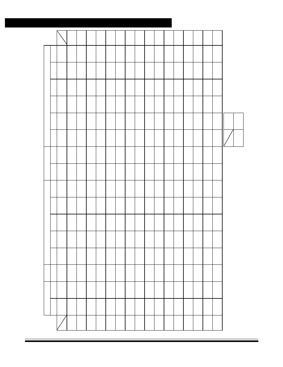
Ad
va
nc
e In
for
m
a
t
ion
M
C68
HC70
5
J
J
7
∑ MC6
8
HC7
05J
P7
-- R
E
V
4
20
8
I
ns
tr
uc
tio
n
S
e
t
M
O
T
O
R
O
L
A
In
st
r
u
c
t
ion S
e
t
Table 14-7. Opcode Map
Bit Manipulation Branch
Read-Modify-Write
Control
Register/Memory
DIR
DIR
REL
DIR
INH
INH
IX1
IX
INH
INH
IMM
DIR
EXT
IX2
IX1
IX
0
1
2
3
4
5
6
7
8
9
A
B
C
D
E
F
0
5
BRSET0
3
DIR
5
BSET0
2
DIR
3
BRA
2
REL
5
NEG
2
DIR
3
NEGA
1
INH
3
NEGX
1
INH
6
NEG
2
IX1
5
NEG
1
IX
9
RTI
1
INH
2
SUB
2
IMM
3
SUB
2
DIR
4
SUB
3
EXT
5
SUB
3
IX2
4
SUB
2
IX1
3
SUB
1
IX
0
1
5
BRCLR0
3
DIR
5
BCLR0
2
DIR
3
BRN
2
REL
6
RTS
1
INH
2
CMP
2
IMM
3
CMP
2
DIR
4
CMP
3
EXT
5
CMP
3
IX2
4
CMP
2
IX1
3
CMP
1
IX
1
2
5
BRSET1
3
DIR
5
BSET1
2
DIR
3
BHI
2
REL
11
MUL
1
INH
2
SBC
2
IMM
3
SBC
2
DIR
4
SBC
3
EXT
5
SBC
3
IX2
4
SBC
2
IX1
3
SBC
1
IX
2
3
5
BRCLR1
3
DIR
5
BCLR1
2
DIR
3
BLS
2
REL
5
COM
2
DIR
3
COMA
1
INH
3
COMX
1
INH
6
COM
2
IX1
5
COM
1
IX
10
SWI
1
INH
2
CPX
2
IMM
3
CPX
2
DIR
4
CPX
3
EXT
5
CPX
3
IX2
4
CPX
2
IX1
3
CPX
1
IX
3
4
5
BRSET2
3
DIR
5
BSET2
2
DIR
3
BCC
2
REL
5
LSR
2
DIR
3
LSRA
1
INH
3
LSRX
1
INH
6
LSR
2
IX1
5
LSR
1
IX
2
AND
2
IMM
3
AND
2
DIR
4
AND
3
EXT
5
AND
3
IX2
4
AND
2
IX1
3
AND
1
IX
4
5
5
BRCLR2
3
DIR
5
BCLR2
2
DIR
3
BCS/BLO
2
REL
2
BIT
2
IMM
3
BIT
2
DIR
4
BIT
3
EXT
5
BIT
3
IX2
4
BIT
2
IX1
3
BIT
1
IX
5
6
5
BRSET3
3
DIR
5
BSET3
2
DIR
3
BNE
2
REL
5
ROR
2
DIR
3
RORA
1
INH
3
RORX
1
INH
6
ROR
2
IX1
5
ROR
1
IX
2
LDA
2
IMM
3
LDA
2
DIR
4
LDA
3
EXT
5
LDA
3
IX2
4
LDA
2
IX1
3
LDA
1
IX
6
7
5
BRCLR3
3
DIR
5
BCLR3
2
DIR
3
BEQ
2
REL
5
ASR
2
DIR
3
ASRA
1
INH
3
ASRX
1
INH
6
ASR
2
IX1
5
ASR
1
IX
2
TAX
1
INH
4
STA
2
DIR
5
STA
3
EXT
6
STA
3
IX2
5
STA
2
IX1
4
STA
1
IX
7
8
5
BRSET4
3
DIR
5
BSET4
2
DIR
3
BHCC
2
REL
5
ASL/LSL
2
DIR
3
ASLA/LSLA
1
INH
3
ASLX/LSLX
1
INH
6
ASL/LSL
2
IX1
5
ASL/LSL
1
IX
2
CLC
1
INH
2
EOR
2
IMM
3
EOR
2
DIR
4
EOR
3
EXT
5
EOR
3
IX2
4
EOR
2
IX1
3
EOR
1
IX
8
9
5
BRCLR4
3
DIR
5
BCLR4
2
DIR
3
BHCS
2
REL
5
ROL
2
DIR
3
ROLA
1
INH
3
ROLX
1
INH
6
ROL
2
IX1
5
ROL
1
IX
2
SEC
1
INH
2
ADC
2
IMM
3
ADC
2
DIR
4
ADC
3
EXT
5
ADC
3
IX2
4
ADC
2
IX1
3
ADC
1
IX
9
A
5
BRSET5
3
DIR
5
BSET5
2
DIR
3
BPL
2
REL
5
DEC
2
DIR
3
DECA
1
INH
3
DECX
1
INH
6
DEC
2
IX1
5
DEC
1
IX
2
CLI
1
INH
2
ORA
2
IMM
3
ORA
2
DIR
4
ORA
3
EXT
5
ORA
3
IX2
4
ORA
2
IX1
3
ORA
1
IX
A
B
5
BRCLR5
3
DIR
5
BCLR5
2
DIR
3
BMI
2
REL
2
SEI
1
INH
2
ADD
2
IMM
3
ADD
2
DIR
4
ADD
3
EXT
5
ADD
3
IX2
4
ADD
2
IX1
3
ADD
1
IX
B
C
5
BRSET6
3
DIR
5
BSET6
2
DIR
3
BMC
2
REL
5
INC
2
DIR
3
INCA
1
INH
3
INCX
1
INH
6
INC
2
IX1
5
INC
1
IX
2
RSP
1
INH
2
JMP
2
DIR
3
JMP
3
EXT
4
JMP
3
IX2
3
JMP
2
IX1
2
JMP
1
IX
C
D
5
BRCLR6
3
DIR
5
BCLR6
2
DIR
3
BMS
2
REL
4
TST
2
DIR
3
TSTA
1
INH
3
TSTX
1
INH
5
TST
2
IX1
4
TST
1
IX
2
NOP
1
INH
6
BSR
2
REL
5
JSR
2
DIR
6
JSR
3
EXT
7
JSR
3
IX2
6
JSR
2
IX1
5
JSR
1
IX
D
E
5
BRSET7
3
DIR
5
BSET7
2
DIR
3
BIL
2
REL
2
STOP
1
INH
2
LDX
2
IMM
3
LDX
2
DIR
4
LDX
3
EXT
5
LDX
3
IX2
4
LDX
2
IX1
3
LDX
1
IX
E
F
5
BRCLR7
3
DIR
5
BCLR7
2
DIR
3
BIH
2
REL
5
CLR
2
DIR
3
CLRA
1
INH
3
CLRX
1
INH
6
CLR
2
IX1
5
CLR
1
IX
2
WAIT
1
INH
2
TXA
1
INH
4
STX
2
DIR
5
STX
3
EXT
6
STX
3
IX2
5
STX
2
IX1
4
STX
1
IX
F
INH = Inherent
REL = Relative
IMM = Immediate
IX = Indexed, No Offset
DIR = Direct
IX1 = Indexed, 8-Bit Offset
EXT = Extended
IX2 = Indexed, 16-Bit Offset
0
MSB of Opcode in Hexadecimal
LSB of Opcode in Hexadecimal
0
5
BRSET0
3
DIR
Number of Cycles
Opcode Mnemonic
Number of Bytes/Addressing Mode
LSB
MSB
LSB
MSB
LSB
MSB

MC68HC705JJ7 ∑ MC68HC705JP7 -- REV 4
Advance Information
MOTOROLA
Electrical Specifications
209
Advance Information -- MC68HC705JJ7/MC68HC705JP7
Section 15. Electrical Specifications
15.1 Contents
15.2
Introduction . . . . . . . . . . . . . . . . . . . . . . . . . . . . . . . . . . . . . . . 210
15.3
Maximum Ratings . . . . . . . . . . . . . . . . . . . . . . . . . . . . . . . . . . 210
15.4
Operating Temperature Range. . . . . . . . . . . . . . . . . . . . . . . . 211
15.5
Thermal Characteristics . . . . . . . . . . . . . . . . . . . . . . . . . . . . . 211
15.6
Supply Current Characteristics
(V
DD
= 4.5 to 5.5 Vdc) . . . . . . . . . . . . . . . . . . . . . . . . . . . . 211
15.7
Supply Current Characteristics
(V
DD
= 2.7 to 3.3 Vdc) . . . . . . . . . . . . . . . . . . . . . . . . . . . . 212
15.8
DC Electrical Characteristics (5.0 Vdc). . . . . . . . . . . . . . . . . . 215
15.9
DC Electrical Characteristics (3.0 Vdc). . . . . . . . . . . . . . . . . . 216
15.10 Analog Subsystem Characteristics (5.0 Vdc) . . . . . . . . . . . . . 217
15.11 Analog Subsystem Characteristics (3.0 Vdc) . . . . . . . . . . . . . 218
15.12 Control Timing (5.0 Vdc). . . . . . . . . . . . . . . . . . . . . . . . . . . . .220
15.13 Control Timing (3.0 Vdc). . . . . . . . . . . . . . . . . . . . . . . . . . . . .221
15.14 PEPROM and EPROM Programming
Characteristics . . . . . . . . . . . . . . . . . . . . . . . . . . . . . . . . . . 224
15.15 SIOP Timing (V
DD
= 5.0 Vdc) . . . . . . . . . . . . . . . . . . . . . . . . . 225
15.16 SIOP Timing (V
DD
= 3.0 Vdc) . . . . . . . . . . . . . . . . . . . . . . . . . 226
15.17 Reset Characteristics . . . . . . . . . . . . . . . . . . . . . . . . . . . . . . . 227

Advance Information
MC68HC705JJ7 ∑ MC68HC705JP7 -- REV 4
210
Electrical Specifications
MOTOROLA
Electrical Specifications
15.2 Introduction
This section contains the electrical and timing specifications.
15.3 Maximum Ratings
Maximum ratings are the extreme limits to which the MCU can be
exposed without permanently damaging it.
The MCU contains circuitry to protect the inputs against damage from
high static voltages; however, do not apply voltages higher than those
shown in the table below. Keep V
In
and V
Out
within the range
V
SS
(V
In
or V
Out
)
V
DD
. Connect unused inputs to the appropriate
voltage level, either V
SS
or V
DD
.
NOTE:
This device is not guaranteed to operate properly at the maximum
ratings. Refer to
15.8 DC Electrical Characteristics (5.0 Vdc)
and
15.9
DC Electrical Characteristics (3.0 Vdc)
for guaranteed operating
conditions.
Rating
Symbol
Value
Unit
Supply voltage
V
DD
≠0.3 to +7.0
V
Bootloader/self-check mode
(IRQ/V
PP
pin only)
V
In
V
SS
≠0.3 to 17
V
Current drain per pin excluding V
DD
and V
SS
I
25
mA
Operating junction temperature
T
J
+150
∞
C
Storage temperature range
T
stg
≠65 to +150
∞
C
Electrical Specifications
Operating Temperature Range
MC68HC705JJ7 ∑ MC68HC705JP7 -- REV 4
Advance Information
MOTOROLA
Electrical Specifications
211
15.4 Operating Temperature Range
15.5 Thermal Characteristics
15.6 Supply Current Characteristics (V
DD
= 4.5 to 5.5 Vdc)
Characteristic
Symbol
Value
Unit
Operating temperature range
Extended
T
A
T
L
to T
H
≠40 to +85
∞
C
Characteristic
Symbol
Value
Unit
Thermal resistance
Plastic DIP
SOIC
JA
60
∞
C/W
Characteristic
(1)
1. V
DD
= 4.5 to 5.5 Vdc, V
SS
= 0 V, T
L
T
A
T
H
, unless otherwise noted. All values shown reflect average measurements.
Symbol
Min
Typ
(2)
2. Typical values at midpoint of voltage range, 25
∞
C only
Max
Unit
RUN
(3)
(analog and LVR disabled)
Internal low-power oscillator at 100 kHz
Internal low-power oscillator at 500 kHz
External oscillator running at 4.2 MHz
3. Run (Operating) I
DD
, Wait I
DD
: Measured using external square wave clock source to OSC1 pin or internal oscillator, all
inputs 0.2 Vdc from either supply rail (V
DD
or V
SS
); no dc loads, less than 50 pF on all outputs, C
L
= 20 pF on OSC2.
I
DD
--
--
--
150
375
3.00
568
1100
5.20
µ
A
µ
A
mA
WAIT
(4)
(analog and LVR disabled)
Internal low-power oscillator at 100 kHz
Internal low-power oscillator at 500 kHz
External oscillator running at 4.2 MHz
4. Wait I
DD
is affected linearly by the OSC2 capacitance.
I
DD
--
--
--
45
75
1.00
85
375
2.20
µ
A
µ
A
mA
STOP
(5)
(analog and LVR disabled)
Typical
≠40
∞
C to 85
∞
C
5. Stop I
DD
: All ports configured as inputs, V
IL
= 0.2 Vdc, V
IH
= V
DD
≠0.2 Vdc, OSC1 = V
DD
.
I
DD
--
--
2
4
10
20
µ
A
Incremental I
DD
for enabled modules
LVR
Analog subsystem
I
DD
--
--
5
380
15
475
µ
A

Advance Information
MC68HC705JJ7 ∑ MC68HC705JP7 -- REV 4
212
Electrical Specifications
MOTOROLA
Electrical Specifications
15.7 Supply Current Characteristics (V
DD
= 2.7 to 3.3 Vdc)
Characteristic
(1)
1. V
DD
= 2.7 to 3.3 Vdc, V
SS
= 0 V, T
L
T
A
T
H
, unless otherwise noted. All values shown reflect average measurements.
Symbol
Min
Typ
(2)
2. Typical values at midpoint of voltage range, 25
∞
C only.
Max
Unit
RUN
(3)
(analog and LVR disabled)
Internal low-power oscillator at 100 kHz
Internal low-power oscillator at 500 kHz
External oscillator running at 2.1 MHz
3. Run (Operating) I
DD
, Wait I
DD
: Measured using external square wave clock source to OSC1 pin or internal oscillator, all
inputs 0.2 Vdc from either supply rail (V
DD
or V
SS
); no dc loads, less than 50 pF on all outputs, C
L
= 20 pF on OSC2.
I
DD
--
--
--
70
320
1.25
320
800
2.60
µ
A
µ
A
mA
WAIT
(4)
(analog and LVR disabled)
Internal low-power oscillator at 100 kHz
Internal low-power oscillator at 500 kHz
External oscillator running at 2.1 MHz
4. Wait I
DD
is affected linearly by the OSC2 capacitance.
I
DD
--
--
--
20
40
0.50
65
250
1.10
µ
A
µ
A
mA
STOP
(5)
(analog and LVR disabled)
25
∞
C
≠40
∞
C to 85
∞
C
5. Stop I
DD
: All ports configured as inputs, V
IL
= 0.2 Vdc, V
IH
= V
DD
≠0.2 Vdc, OSC1 = V
DD
.
I
DD
--
--
1
2
5
10
µ
A
Incremental I
DD
for enabled modules
LVR
Analog subsystem
I
DD
--
--
5
380
15
475
µ
A
Electrical Specifications
Supply Current Characteristics (V
DD
= 2.7 to 3.3 Vdc)
MC68HC705JJ7 ∑ MC68HC705JP7 -- REV 4
Advance Information
MOTOROLA
Electrical Specifications
213
Figure 15-1. Typical Run I
DD
versus Internal
Clock Frequency at 25
∞
C
Figure 15-2. Typical Wait I
DD
versus Internal
Clock Frequency at 25
∞
C
0.00E+00
5.00E≠04
1.00E≠03
1.50E≠03
2.00E≠03
2.50E≠03
3.00E≠03
3.50E≠03
0
0.5
1
1.5
2
2.5
FREQUENCY IN MHz
5.5 V
4.5 V
3.3 V
2.7 V
SU
PP
LY
CU
RR
E
N
T
I
N
AM
PS
0.00E+00
2.00E≠04
4.00E≠04
6.00E≠04
8.00E≠04
1.00E≠03
1.20E≠03
1.40E≠03
1.60E≠03
0
0.5
1
1.5
2
2.5
FREQUENCY IN MHz
5.5 V
4.5 V
3.3 V
2.7 V
SU
PP
LY CUR
RE
NT
IN AM
PS

Advance Information
MC68HC705JJ7 ∑ MC68HC705JP7 -- REV 4
214
Electrical Specifications
MOTOROLA
Electrical Specifications
Figure 15-3. Typical Run I
DD
with External Oscillator
Figure 15-4. Typical Wait I
DD
with External Oscillator
Figure 15-5. Typical Stop I
DD
with Analog and LVR Disabled
5.00E≠04
1.00E≠03
1.50E≠03
2.00E≠03
2.50E≠03
3.00E≠03
3.50E≠03
2.5
3
3.5
4
4.5
5
5.5
6
SUPPLY VOLTAGE IN VOLTS
≠40
∞
C
25
∞
C
85
∞
C
S
U
PP
LY
CU
RR
EN
T
I
N
AM
PS
2.00E≠04
4.00E≠04
6.00E≠04
8.00E≠04
1.00E≠03
1.20E≠03
1.40E≠03
1.60E≠03
1.80E≠03
2.5
3
3.5
4
4.5
5
5.5
6
SUPPLY VOLTAGE IN VOLTS
SU
PP
L
Y
CU
R
R
E
N
T
IN
AM
PS
≠40
∞
C
25
∞
C
85
∞
C
0.00E+00
5.00E≠07
1.00E≠06
1.50E≠06
2.00E≠06
2.50E≠06
3.00E≠06
3.50E≠06
4.00E≠06
4.50E≠06
2.5
3
3.5
4
4.5
5
5.5
6
SUPPLY VOLTAGE IN VOLTS
≠40
∞
C
25
∞
C
85
∞
C
SU
PP
L
Y
C
U
R
R
E
N
T
I
N
AM
P
S
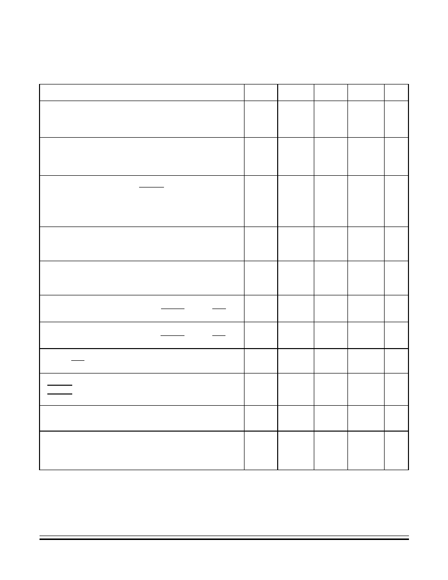
Electrical Specifications
DC Electrical Characteristics (5.0 Vdc)
MC68HC705JJ7 ∑ MC68HC705JP7 -- REV 4
Advance Information
MOTOROLA
Electrical Specifications
215
15.8 DC Electrical Characteristics (5.0 Vdc)
Characteristic
(1),
(2)
1. +4.5
V
DD
+5.5 V, V
SS
= 0 V, T
L
T
A
T
H
, unless otherwise noted
2. All values shown reflect average measurements.
Symbol
Min
Typ
(3)
3. Typical values at midpoint of voltage range, 25
∞
C only.
Max
Unit
Output voltage
ILoad = 10.0
µ
A
ILoad = ≠10.0
µ
A
V
OL
V
OH
--
V
DD
≠0.1
--
--
0.1
--
V
Output high voltage
(ILoad = ≠0.8 mA) PB0≠PB7
(ILoad = ≠4.0 mA) PA0≠PA5, PB4, PC0≠PC7
(4)
4. PC0≠PC7 parameters only apply to MC68HC705JP7.
V
OH
V
DD
≠0.8
V
DD
≠0.8
--
--
--
--
V
Output low voltage
(ILoad = 1.6 mA) PB0≠PB7, RESET
(ILoad = 10 mA) PA0≠PA5, PB4, PC0≠PC7
(4)
(ILoad = 15 mA) PA0≠PA5, PB4, PC0≠PC7
(4)
V
OL
--
--
--
--
--
--
0.4
0.4
1.5
V
High source current
Total for all (6) PA0≠PA5 pins and PB4
Total for all (8) PC0≠PC7
(4)
pins
I
OH
--
--
--
--
20
30
mA
High sink current
Total for all (6) PA0≠PA5 pins and PB4
Total for all (8) PC0≠PC7
(4)
pins
I
OL
--
--
--
--
40
60
mA
Input high voltage
PA0≠PA5, PB0≠PB7, PC0≠PC7
(4)
, RESET, OSC1, IRQ/V
PP
V
IH
0.7 x V
DD
--
V
DD
V
Input low voltage
PA0≠PA5, PB0≠PB7, PC0≠PC7
(4)
, RESET, OSC1, IRQ/V
PP
V
IL
V
SS
--
0.3 x V
DD
V
Input current
OSC1, IRQ/V
PP
I
In
≠1
--
1
µ
A
Input current
RESET (pullup, source)
RESET (pulldown, sink)
I
In
10
≠6
--
--
--
--
µ
A
mA
I/O ports hi-Z leakage current (pulldowns off)
PA0≠PA6, PB0≠PB7, PC0≠PC7
(4)
I
OZ
≠2
--
2
µ
A
Input pulldown current
PA0≠PA5, PB0≠PB7, PC0≠PC7
(4)
(V
In
; V
IH
= 0.7 x V
DD
)
PA0≠PA5, PB0≠PB7, PC0≠PC7
(4)
(V
In
; V
IL
= 0.3 x V
DD
)
I
IL
40
25
100
65
280
190
µ
A

Advance Information
MC68HC705JJ7 ∑ MC68HC705JP7 -- REV 4
216
Electrical Specifications
MOTOROLA
Electrical Specifications
15.9 DC Electrical Characteristics (3.0 Vdc)
Characteristic
(1),
(2)
1. +2.7
V
DD
+3.3 V, V
SS
= 0 V, T
L
T
A
T
H
, unless otherwise noted
2. All values shown reflect average measurements.
Symbol
Min
Typ
(3)
3. Typical values at midpoint of voltage range, 25
∞
C only.
Max
Unit
Output voltage
ILoad = 10.0
µ
A
ILoad = ≠10.0
µ
A
V
OL
V
OH
--
V
DD
≠0.1
--
--
0.1
--
V
Output high voltage
(ILoad = ≠0.2 mA) PB0≠PB7
(ILoad = ≠2.0 mA) PA0≠PA5, PB4, PC0≠PC7
(4)
4. PC0≠PC7 parameters only apply to MC68HC705JP7.
V
OH
V
DD
≠0.8
V
DD
≠0.8
--
--
--
--
V
Output low voltage
(ILoad = 1.6 mA) PB0≠PB7, RESET
(ILoad = 5 mA) PA0≠PA5, PB4, PC0≠PC7
(4)
V
OL
--
--
--
--
0.3
0.3
V
High source current
Total for all (6) PA0≠PA5 pins and PB4
Total for all (8) PC0≠PC7
(4)
pins
I
OH
--
--
--
--
20
30
mA
High sink current
Total for all (6) PA0≠PA5 pins and PB4
Total for all (8) PC0≠PC7
(4)
pins
I
OL
--
--
--
--
40
60
mA
Input high voltage
PA0≠PA5, PB0≠PB7, PC0≠PC7
(4)
, RESET, OSC1, IRQ/V
PP
V
IH
0.7 x V
DD
--
V
DD
V
Input low voltage
PA0≠PA5, PB0≠PB7, PC0≠PC7
(4)
, RESET, OSC1, IRQ/V
PP
V
IL
V
SS
--
0.2 x V
DD
V
Input current
OSC1, IRQ/V
PP
I
In
≠1
--
1
µ
A
Input current
RESET (pullup, source)
RESET (pulldown, sink)
I
In
5
≠3
--
--
--
--
µ
A
mA
I/O ports hi-Z leakage current (pulldowns off)
PA0≠PA6, PB0≠PB7, PC0≠PC7
(4)
I
OZ
≠2
--
2
µ
A
Input pulldown current
PA0≠PA5, PB0≠PB7, PC0≠PC7
(4)
(V
In
; V
IH
= 0.7 x V
DD
)
PA0≠PA5, PB0≠PB7, PC0≠PC7
(4)
(V
In
; V
IL
= 0.3 x V
DD
)
I
IL
10
4
25
20
75
40
µ
A

Electrical Specifications
Analog Subsystem Characteristics (5.0 Vdc)
MC68HC705JJ7 ∑ MC68HC705JP7 -- REV 4
Advance Information
MOTOROLA
Electrical Specifications
217
15.10 Analog Subsystem Characteristics (5.0 Vdc)
NOTE:
See
Figure 15-6
.
Characteristic
(1)
Symbol
Min
Max
Unit
Voltage comparators
Input offset voltage
Common-mode range
Comparator 1 input impedance
Comparator 2 input impedance
Direct input to comparator 2 (HOLD = 1, DHOLD = 0)
Divider input to comparator 2 (HOLD = 0, DHOLD = 1)
V
IO
V
CMR
Z
In
Z
In
Z
In
--
--
800
800
80
15
V
DD
≠1.5
--
--
--
mV
V
k
k
k
Input divider ratio (comparator 2, HOLD = 0, DHOLD =1)
V
In
= 0 to V
DD
≠1.5 V
R
DIV
0.49
0.51
Analog subsystem internal V
SS
offset
Sum of comparator offset and IR drop through V
SS
V
AOFF
20
40
mV
Channel selection multiplexer switch resistance
R
MUX
--
3
k
External current source (PB0/AN0)
Source current (V
Out
= V
DD
/2)
Source current linearity (V
Out
= 0 to V
DD
≠1.5 Vdc)
Discharge sink current (V
Out
= 0.4 V)
I
CHG
I
CHG
I
DIS
85
--
1.1
113
±1
--
µ
A
%FS
mA
External capacitor (connected to PB0/AN0)
Voltage range
Discharge time
Value of external ramping capacitor
V
CAP
t
DIS
C
EXT
V
SS
5
--
V
DD
≠1.5
10
2
V
ms/
µ
F
µ
F
Internal sample and hold capacitor
Capacitance
Charge/discharge time (0 to 3.5 Vdc)
Direct connection (HOLD = 1, DHOLD = 0)
Divided connection (HOLD = 0, DHOLD = 1)
Temperature diode connection (HOLD = 1, DHOLD = 1)
Leakage discharge rate
C
SH
t
SHCHG
t
SHDCHG
t
SHTCHG
C
SHDIS
8
1
2
1
--
13
--
--
--
0.2
pF
µ
s
µ
s
µ
s
V/sec
Internal temperature sensing diode
Voltage at T
J
= 25
∞
C
Temperature change in voltage
V
D
TC
D
0.65
1.8
0.71
2.0
V
mV/
∞
C
1. +4.5
V
DD
+5.5 V, V
SS
= 0 V, T
L
T
A
T
H
, unless otherwise noted
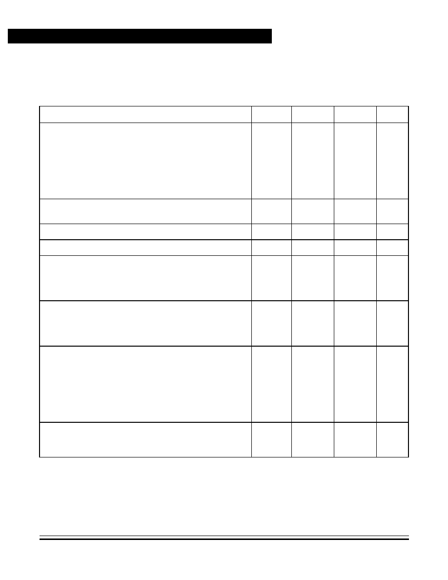
Advance Information
MC68HC705JJ7 ∑ MC68HC705JP7 -- REV 4
218
Electrical Specifications
MOTOROLA
Electrical Specifications
15.11 Analog Subsystem Characteristics (3.0 Vdc)
NOTE:
See
Figure 15-6
.
Characteristic
(1)
Symbol
Min
Max
Unit
Voltage comparators
Input offset voltage
Common-mode range
Comparator 1 input impedance
Comparator 2 input impedance
Direct input to comparator 2 (HOLD = 1, DHOLD = 0)
Divider input to comparator 2 (HOLD = 0, DHOLD = 1)
V
IO
V
CMR
Z
In
Z
In
Z
In
--
--
800
800
80
15
V
DD
≠1.5
--
--
--
mV
V
k
k
k
Input divider ratio (comparator 2, HOLD = 0, DHOLD =1)
V
In
= 0 to V
DD
≠1.5 V
R
DIV
0.49
0.51
Analog subsystem internal V
SS
offset
V
AOFF
10
30
mV
Multiplexer switch resistance
R
MUX
--
5
k
External current source (PB0/AN0)
Source current (V
Out
= V
DD
/2)
Source current linearity (V
Out
= 0 to V
DD
≠1.5 Vdc)
Discharge sink current (V
Out
= 0.4 V)
I
CHG
I
CHG
I
DIS
75
--
1
104
±
1
--
µ
A
%FS
mA
External capacitor (connected to PB0/AN0)
Voltage range
Discharge time
Value of external ramping capacitor
V
CAP
t
DIS
C
EXT
V
SS
5
--
V
DD
≠1.5
10
2
V
ms/
µ
F
µ
F
Internal sample and hold capacitor
Capacitance
Charge/discharge time (0 to 3.5 Vdc)
Direct connection (HOLD = 1, DHOLD = 0)
Divided connection (HOLD = 0, DHOLD = 1)
Temperature diode connection (HOLD = 1, DHOLD = 1)
Leakage discharge rate
C
SH
t
SHCHG
t
SHDCHG
t
SHTCHG
C
SHDIS
8
1
2
1
--
13
--
--
--
0.1
pF
µ
s
µ
s
µ
s
V/sec
Internal temperature sensing diode
Voltage at T
J
= 25
∞
C
Temperature change in voltage
V
D
TC
D
0.65
1.8
0.71
2.0
V
mV/
∞
C
1. +2.7
V
DD
+3.3 V, V
SS
= 0 V, T
L
T
A
T
H
, unless otherwise noted
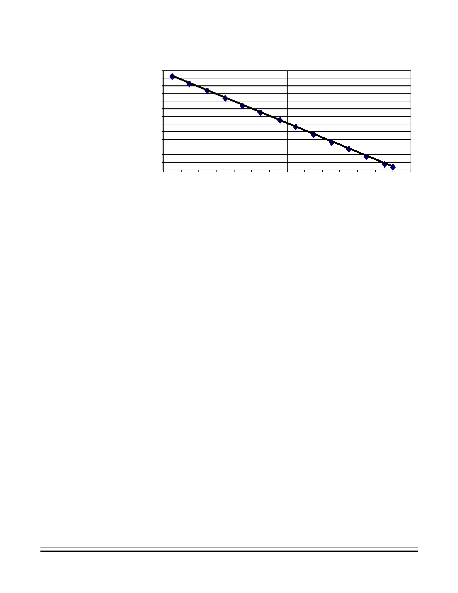
Electrical Specifications
Analog Subsystem Characteristics (3.0 Vdc)
MC68HC705JJ7 ∑ MC68HC705JP7 -- REV 4
Advance Information
MOTOROLA
Electrical Specifications
219
Figure 15-6. Typical Temperature Diode Performance
680
700
560
580
600
620
640
660
720
740
760
780
800
820
≠45
≠35
≠25
≠15
≠5
5
15
25
35
45
55
65
75
85
95
TEMPERATURE IN
∞
C
T
DI
O
D
E
IN
mV

Advance Information
MC68HC705JJ7 ∑ MC68HC705JP7 -- REV 4
220
Electrical Specifications
MOTOROLA
Electrical Specifications
15.12 Control Timing (5.0 Vdc)
Characteristic
(1)
1. V
DD
= 4.5 to 5.5 Vdc, V
SS
= 0 V, T
L
T
A
T
H
, unless otherwise noted
Symbol
Min
Max
Unit
Frequency of oscillation (OSC)
RC oscillator option
Crystal oscillator option
External clock source
Internal low-power oscillator
Standard product (100 kHz nominal)
Mask option (500 kHz nominal, see Note 3)
f
OSC
--
0.1
dc
60
300
4.2
4.2
4.2
140
700
MHz
MHz
MHz
kHz
kHz
Internal operating frequency, crystal, or external clock (f
OSC
/2)
RC oscillator option
Crystal oscillator option
External clock source
Internal low-power oscillator
Standard product (100 kHz nominal)
Mask option (500 kHz nominal
(2)
)
f
OP
--
0.05
dc
30
150
2.1
2.1
2.1
75
350
MHz
MHz
MHz
kHz
kHz
Cycle time (1/f
OP
)
External oscillator or clock source
Internal low-power oscillator
Standard product (100 kHz nominal)
Mask option (500 kHz nominal
(2)
)
2. The 500-kHz nominal mask option is available through special order only. Contact your local Motorola sales representative
for detailed ordering information. Not offered with the RC oscillator.
t
cyc
476
14.29
2.86
--
33.33
6.67
ns
µ
s
µ
s
16-bit timer
Resolution
Input capture (TCAP) pulse width
t
RESL
t
TH
, t
TL
4.0
284
--
--
t
cyc
ns
Interrupt pulse width low (edge-triggered)
t
ILIH
284
--
ns
Interrupt pulse period
t
ILIL
(3)
3. The minimum period, t
ILIL
, should not be less than the number of cycle times it takes to execute the interrupt service routine
plus 21
t
cyc
.
--
t
cyc
OSC1 pulse width (external clock input)
t
OH
, t
OL
110
--
ns
Analog subsystem response
Voltage comparators
Switching time (10 mV overdrive, either input)
Comparator power-up delay (bias circuit already powered up)
External current source (PB0/AN0)
Switching time (I
DIS
to I
RAMP
)
Power-up delay (bias circuit already powered up)
Bias circuit power-up delay
t
CPROP
t
CDELAY
t
ISTART
t
IDELAY
t
BDELAY
--
--
--
--
--
2
2
1
2
2
µ
s
µ
s
µ
s
µ
s
µ
s
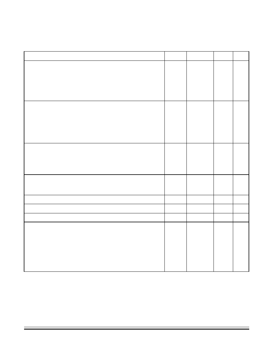
Electrical Specifications
Control Timing (3.0 Vdc)
MC68HC705JJ7 ∑ MC68HC705JP7 -- REV 4
Advance Information
MOTOROLA
Electrical Specifications
221
15.13 Control Timing (3.0 Vdc)
Characteristic
(1)
1. +2.7
V
DD
+3.3 V, V
SS
= 0 V, T
L
T
A
T
H
, unless otherwise noted
Symbol
Min
Max
Unit
Frequency of oscillation (OSC)
RC oscillator option
Crystal oscillator option
External clock source
Internal low-power oscillator
Standard product (100 kHz nominal)
Mask option (500 kHz nominal, see Note 3))
f
OSC
--
0.1
dc
60
300
2.1
2.1
2.1
140
700
MHz
MHz
MHz
kHz
kHz
Internal operating frequency, crystal, or external clock (f
OSC
/2)
RC oscillator option
Crystal oscillator option
External clock source
Internal low-power oscillator
Standard product (100 kHz nominal)
Mask option (500 kHz nominal
(2)
)
2. The 500 kHz nominal mask option is available through special order only. Contact your local Motorola sales representative
for detailed ordering information. Not offered with the RC oscillator option.
f
OP
--
0.05
dc
30
150
1.05
1.05
1.05
70
350
MHz
MHz
MHz
kHz
kHz
Cycle time (1/f
OP
)
External oscillator or clock source
Internal low-power oscillator
Standard product (100 kHz nominal)
Mask option (500 kHz nominal
(2)
)
t
cyc
952
14.29
2.86
--
33.33
6.67
ns
µ
s
µ
s
16-bit timer
Resolution
Input capture (TCAP) pulse width
t
RESL
t
TH
, t
TL
4.0
284
--
--
t
cyc
ns
Interrupt pulse width low (edge-triggered)
t
ILIH
284
--
ns
Interrupt pulse period
t
ILIL
(3)
3. The minimum period, t
ILIL
, should not be less than the number of cycle times it takes to execute the interrupt service routine
plus 21
t
cyc
.
--
t
cyc
OSC1 pulse width (external clock input)
t
OH
, t
OL
110
--
ns
Analog subsystem response
Voltage comparators
Switching time (10 mV overdrive, either input)
Comparator power-up delay (bias circuit already powered up)
External current source (PB0/AN0)
Switching time (I
DIS
to I
RAMP
)
Power-up delay (bias circuit already powered up)
Bias circuit power-up delay
t
CPROP
t
CDELAY
t
ISTART
t
IDELAY
t
BDELAY
--
--
--
--
--
2
2
1
2
2
µ
s
µ
s
µ
s
µ
s
µ
s

Advance Information
MC68HC705JJ7 ∑ MC68HC705JP7 -- REV 4
222
Electrical Specifications
MOTOROLA
Electrical Specifications
Figure 15-7. Typical 500 kHz External Low-Power
Oscillator Frequency
Figure 15-8. Typical 100 kHz External Low-Power
Oscillator Frequency
420000
430000
440000
450000
460000
470000
480000
490000
500000
510000
≠45
≠35
≠25
≠15
≠5
5
15
25
35
45
55
65
75
85
95
TEMPERATURE IN
∞
C
F
R
EQ
UE
NC
Y I
N
H
z
109500
110000
110500
111000
111500
112000
112500
113000
113500
114000
≠45
≠35
≠25
≠15
≠5
5
15
25
35
45
55
65
75
85
95
TEMPERATURE IN
∞
C
FR
EQ
UE
NCY
IN
Hz
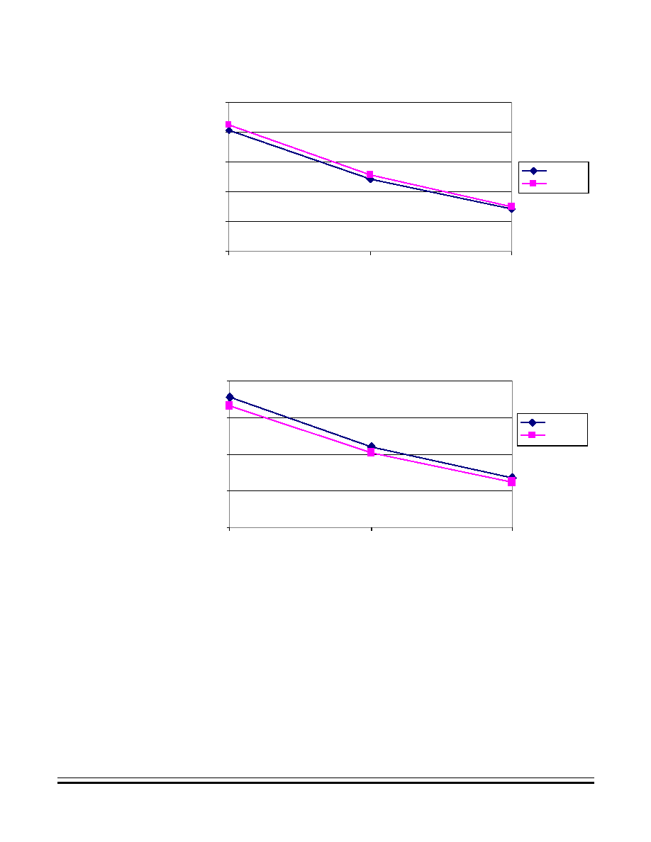
Electrical Specifications
Control Timing (3.0 Vdc)
MC68HC705JJ7 ∑ MC68HC705JP7 -- REV 4
Advance Information
MOTOROLA
Electrical Specifications
223
Figure 15-9. Typical RC Oscillator Internal Operating
Frequency Range versus Resistance for High V
DD
Operating Range at T = 25
∞
C
Figure 15-10. Typical RC Oscillator Internal Operating
Frequency Range versus Resistance for Low V
DD
Operating Range at T = 25
∞
C
0
0.5
1
1.5
2
2.5
12.1
24.9
49.9
EXTERNAL RESISTOR VALUE (k
)
V
DD
= 5.5 V
V
DD
= 4.5 V
I
N
T
E
RN
AL
BUS
FR
EQU
E
N
C
Y
(MH
z
)
0
0.5
1
1.5
2
12.1
24.9
49.9
EXTERNAL RESISTOR VALUE (k
)
V
DD
= 3.3 V
V
DD
= 2.7 V
IN
TE
RN
AL
BU
S F
R
E
Q
UE
NC
Y (
M
H
z
)

Advance Information
MC68HC705JJ7 ∑ MC68HC705JP7 -- REV 4
224
Electrical Specifications
MOTOROLA
Electrical Specifications
15.14 PEPROM and EPROM Programming Characteristics
NOTE:
To program the EPROM/OTPROM, MOR, or EPMSEC bits, the voltage
on V
DD
must be greater than 4.5 volts.
Characteristic
(1)
1. +4.5
V
DD
+5.5 V, V
SS
= 0 V, T
L
T
A
T
H
, unless otherwise noted
Symbol
Min
Typ
Max
Unit
PEPROM programming voltage (IRQ/V
PP
)
V
PP
16.0
16.5
17.0
V
PEPROM programming voltage (IRQ/V
PP
)
I
PP
--
3.0
5.0
mA
PEPROM programming time per bit
t
EPGM
4.0
--
--
ms
EPROM/MOR programming voltage (IRQ/V
PP
)
V
PP
16.0
16.5
17.0
V
EPROM/MOR programming current (IRQ/V
PP
)
I
PP
--
3.0
5.0
mA
EPROM programming time per byte
t
EPGM
4.0
--
--
ms
MOR programming time
t
MPGM
10.0
--
--
ms
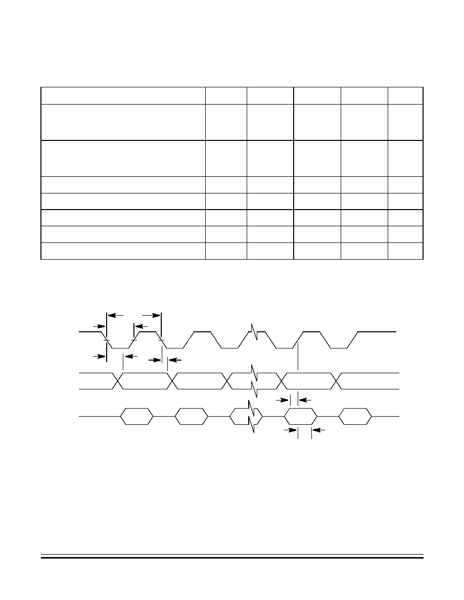
Electrical Specifications
SIOP Timing (VDD = 5.0 Vdc)
MC68HC705JJ7 ∑ MC68HC705JP7 -- REV 4
Advance Information
MOTOROLA
Electrical Specifications
225
15.15 SIOP Timing (V
DD
= 5.0 Vdc)
Figure 15-11. SIOP Timing Diagram
Characteristic
(1)
1. +4.5
V
DD
+5.5 V, V
SS
= 0 V, T
L
T
A
T
H
, unless otherwise noted
Symbol
Min
Typ
Max
Unit
Frequency of operation
Master
Slave
f
SIOP(M)
f
SIOP(S)
0.25 x f
OP
dc
0.25 x f
OP
--
0.25 x f
OP
1050
kHz
Cycle time
Master
Slave
t
SCK(M)
t
SCK(M)
4.0 x t
cyc
--
4.0 x t
cyc
--
4.0 x t
cyc
3.8
µ
s
Clock (SCK) low time (f
OP
= 4.2 MHz)
t
SCKL
952
--
--
ns
SDO data valid time
t
V
--
--
200
ns
SDO hold time
t
HO
0
--
--
ns
SDI setup time
t
S
100
--
--
ns
SDI hold time
t
H
100
--
--
ns
t
SCK
SCK
t
SCKL
t
V
t
HO
SDO
MSB
BIT 1
LSB
t
H
t
S
SDI
MSB
LSB
VALID DATA

Advance Information
MC68HC705JJ7 ∑ MC68HC705JP7 -- REV 4
226
Electrical Specifications
MOTOROLA
Electrical Specifications
15.16 SIOP Timing (V
DD
= 3.0 Vdc)
Characteristic
(1)
1. +2.7
V
DD
+3.3 V, V
SS
= 0 V, T
L
T
A
T
H
, unless otherwise noted
Symbol
Min
Typ
Max
Unit
Frequency of operation
Master
Slave
f
SIOP(M)
f
SIOP(S)
0.25 x f
OP
dc
0.25 x f
OP
--
0.25 x f
OP
525
kHz
Cycle time
Master
Slave
t
SCK(M)
t
SCK(M)
4.0 x t
cyc
--
4.0 x t
cyc
--
4.0 x t
cyc
1.9
µ
s
Clock (SCK) low time (f
OP
= 2.1 MHz)
t
SCKL
1905
--
--
ns
SDO data valid time
t
V
--
--
400
ns
SDO hold time
t
HO
0
--
--
ns
SDI setup time
t
S
200
--
--
ns
SDI hold time
t
H
200
--
--
ns
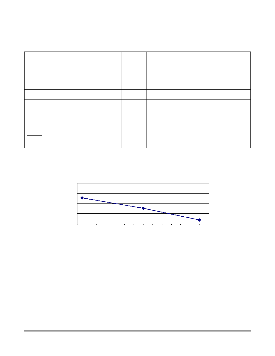
Electrical Specifications
Reset Characteristics
MC68HC705JJ7 ∑ MC68HC705JP7 -- REV 4
Advance Information
MOTOROLA
Electrical Specifications
227
15.17 Reset Characteristics
Figure 15-12. Typical Falling Low Voltage Reset
Characteristic
(1)
1. +2.7
V
DD
+3.3 V, V
SS
= 0 V, T
L
T
A
T
H
, unless otherwise noted
Symbol
Min
Typ
Max
Unit
Low-voltage reset
Rising recovery voltage
Falling reset voltage
LVR hysteresis
V
LVRR
V
LVRF
V
LVRH
2.4
2.3
30
3.4
3.3
70
4.4
4.3
--
V
V
mV
POR recovery voltage
(2)
2. By design, not tested
V
POR
0
--
100
mV
POR V
DD
slew rate
(2)
Rising
(2)
Falling
(2)
S
VDDR
S
VDDF
--
--
--
--
0.1
0.05
V/
µ
s
RESET pulse width (when bus clock active)
t
RL
1.5
--
--
t
CYC
RESET pulldown pulse width from internal
reset
t
RPD
3
--
4
t
CYC
2.5
3
3.5
4
4.5
≠45
≠35
≠25
≠15
≠5
5
15
25
35
45
55
65
75
85
95
TEMPERATURE IN
∞
C
RE
S
E
T
VO
LT
AG
E I
N
V
O
L
T
S
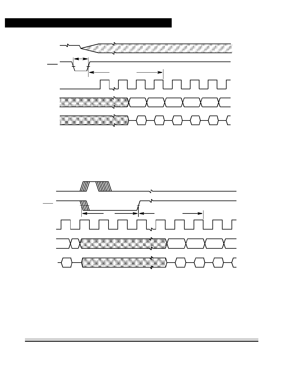
Advance Information
MC68HC705JJ7 ∑ MC68HC705JP7 -- REV 4
228
Electrical Specifications
MOTOROLA
Electrical Specifications
Figure 15-13. Stop Recovery Timing Diagram
Figure 15-14. Internal Reset Timing Diagram
PCH
NEW
1FFE
t
RL
OSC1
1
RESET
INTERNAL
CLOCK
(3)
INTERNAL
ADDRESS
BUS
(3)
4064 or 16 t
cyc
(2)
Notes:
1. Represents the internal gating of the OSC1 pin
2. Normal delay of 4064 t
cyc
or short delay option of 16 t
cyc
3. Internal timing signal and data information not available externally
INTERNAL
DATA
BUS
(3)
1FFF
NEW PCH
NEW PCL
PCL
NEW
code
Op
PCH
NEW
1FFE
t
RPD
RESET
INTERNAL
CLOCK
(3)
INTERNAL
ADDRESS
BUS
(3)
4064 or 16 t
cyc
(2)
Notes:
1.Represents the internal reset from low-voltage reset, illegal opcode fetch or COP watchdog timeout
2.Only if reset occurs during normal delay of 4064 t
CYC
or short delay option of 16 t
CYC
for initial power-up
or stop recovery.
3.Internal timing signal and data information not available externally
INTERNAL
DATA
BUS
(3)
1FFF
NEW PCH
NEW PCL
PCL
NEW
INTERNAL
RESET
1
PIN

Electrical Specifications
Reset Characteristics
MC68HC705JJ7 ∑ MC68HC705JP7 -- REV 4
Advance Information
MOTOROLA
Electrical Specifications
229
Figure 15-15. Low-Voltage Reset Timing Diagram
PCH
NEW
1FFE
t
RPD
RESET
INTERNAL
CLOCK
3
INTERNAL
ADDRESS
BUS
(3)
4064 or 16 t
cyc
(2)
Notes:
1. RESET pin pulled down by internal device
2 Only if LVR occurs during normal delay of 4064 t
cyc
or short delay option of 16 t
cyc
for initial power-up
or stop recovery.
3 Internal timing signal and data information not available externally
INTERNAL
DATA
BUS
(3)
1FFF
NEW PCH
NEW PCL
PCL
NEW
V
DD
PIN
1
LOW
VOLTAGE
RESET
V
LVRR
V
LVRF

Advance Information
MC68HC705JJ7 ∑ MC68HC705JP7 -- REV 4
230
Electrical Specifications
MOTOROLA
Electrical Specifications

MC68HC705JJ7 ∑ MC68HC705JP7 -- REV 4
Advance Information
MOTOROLA
Mechanical Specifications
231
Advance Information -- MC68HC705JJ7/MC68HC705JP7
Section 16. Mechanical Specifications
16.1 Contents
16.2
Introduction . . . . . . . . . . . . . . . . . . . . . . . . . . . . . . . . . . . . . . . 231
16.3
20-Pin Plastic Dual In-Line Package (Case 738) . . . . . . . . . . 232
16.4
20-Pin Small Outline Integrated Circuit (Case 751D) . . . . . . . 233
16.5
28-Pin Plastic Dual In-Line Package (Case 710) . . . . . . . . . . 233
16.6
28-Pin Small Outline Integrated Circuit (Case 751F) . . . . . . . 234
16.7
20-Pin Windowed Ceramic Integrated Circuit
(Case 732) . . . . . . . . . . . . . . . . . . . . . . . . . . . . . . . . . . . . . 234
16.8
28-Pin Windowed Ceramic Integrated Circuit
(Case 733A). . . . . . . . . . . . . . . . . . . . . . . . . . . . . . . . . . . .235
16.2 Introduction
The MC68HC705JJ7 is available in:
∑
20-pin plastic dual in-line package (PDIP)
∑
20-pin small outline integrated circuit (SOIC) package
∑
20-pin windowed ceramic package
The MC68HC705JP7 is available in:
∑
28-pin plastic dual in-line package (PDIP)
∑
28-pin small outline integrated circuit (SOIC) package
∑
28-pin windowed ceramic package

Advance Information
MC68HC705JJ7 ∑ MC68HC705JP7 -- REV 4
232
Mechanical Specifications
MOTOROLA
Mechanical Specifications
The following figures show the latest packages at the time of this
publication. To make sure that you have the latest case outline
specifications, contact one of the following:
∑
Local Motorola Sales Office
∑
World Wide Web at:
http://
www.motorola.com/mcu/
Follow World Wide Web on-line instructions to retrieve the current
mechanical specifications.
16.3 20-Pin Plastic Dual In-Line Package (Case 738)
1.070
0.260
0.180
0.022
0.070
0.015
0.140
15
∞
0.040
1.010
0.240
0.150
0.015
0.050
0.008
0.110
0
∞
0.020
25.66
6.10
3.81
0.39
1.27
0.21
2.80
0
∞
0.51
27.17
6.60
4.57
0.55
1.77
0.38
3.55
15
∞
1.01
0.050 BSC
0.100 BSC
0.300 BSC
1.27 BSC
2.54 BSC
7.62 BSC
MIN
MIN
MAX
MAX
INCHES
MILLIMETERS
DIM
A
B
C
D
E
F
G
J
K
L
M
N
NOTES:
1. DIMENSIONING AND TOLERANCING PER ANSI
Y14.5M, 1982.
2. CONTROLLING DIMENSION: INCH.
3. DIMENSION L TO CENTER OF LEAD WHEN
FORMED PARALLEL.
4. DIMENSION B DOES NOT INCLUDE MOLD
FLASH.
-A-
C
K
N
E
G
F
D
20 PL
J
20 PL
L
M
-T-
SEATING
PLANE
1
10
11
20
0.25 (0.010)
T A
M
M
0.25 (0.010)
T B
M
M
B

Mechanical Specifications
20-Pin Small Outline Integrated Circuit (Case 751D)
MC68HC705JJ7 ∑ MC68HC705JP7 -- REV 4
Advance Information
MOTOROLA
Mechanical Specifications
233
16.4 20-Pin Small Outline Integrated Circuit (Case 751D)
16.5 28-Pin Plastic Dual In-Line Package (Case 710)
MIN
MIN
MAX
MAX
MILLIMETERS
INCHES
DIM
A
B
C
D
F
G
J
K
M
P
R
0.510
0.299
0.104
0.019
0.035
0.012
0.009
7
∞
0.415
0.029
0.499
0.292
0.093
0.014
0.020
0.010
0.004
0
∞
0.395
0.010
12.95
7.60
2.65
0.49
0.90
0.32
0.25
7
∞
10.55
0.75
12.65
7.40
2.35
0.35
0.50
0.25
0.10
0
∞
10.05
0.25
NOTES:
1. DIMENSIONING AND TOLERANCING PER
ANSI Y14.5M, 1982.
2. CONTROLLING DIMENSION: MILLIMETER.
3. DIMENSIONS A AND B DO NOT INCLUDE
MOLD PROTRUSION.
4. MAXIMUM MOLD PROTRUSION 0.150
(0.006) PER SIDE.
5. DIMENSION D DOES NOT INCLUDE
DAMBAR PROTRUSION. ALLOWABLE
DAMBAR PROTRUSION SHALL BE 0.13
(0.005) TOTAL IN EXCESS OF D DIMENSION
AT MAXIMUM MATERIAL CONDITION.
1.27 BSC
0.050 BSC
-A-
-B-
P
10 PL
1
10
11
20
-T-
D
20 PL
K
C
SEATING
PLANE
R
X 45
∞
M
0.010 (0.25)
B
M
M
0.010 (0.25)
T A
B
M
S
S
G
18 PL
F
J
0.100 BSC
0.600 BSC
2.54 BSC
15.24 BSC
MIN
MIN
MAX
MAX
MILLIMETERS
INCHES
DIM
36.45
13.72
3.94
0.36
1.02
1.65
0.20
2.92
0
∞
0.51
37.21
14.22
5.08
0.56
1.52
2.16
0.38
3.43
15
∞
1.02
1.435
0.540
0.155
0.014
0.040
0.065
0.008
0.115
0
∞
0.020
1.465
0.560
0.200
0.022
0.060
0.085
0.015
0.135
15
∞
0.040
A
B
C
D
F
G
H
J
K
L
M
N
NOTES:
1. POSITIONAL TOLERANCE OF LEADS (D),
SHALL BE WITHIN 0.25mm (0.010) AT
MAXIMUM MATERIAL CONDITION, IN
RELATION TO SEATING PLANE AND
EACH OTHER.
2. DIMENSION L TO CENTER OF LEADS
WHEN FORMED PARALLEL.
3. DIMENSION B DOES NOT INCLUDE
MOLD FLASH.
1
14
15
28
B
A
C
N
K
M
J
D
SEATING
PLANE
F
H
G
L
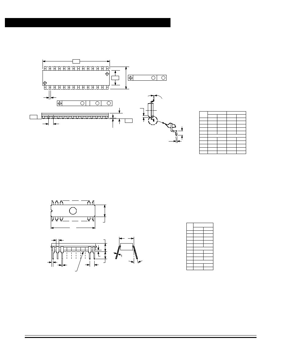
Advance Information
MC68HC705JJ7 ∑ MC68HC705JP7 -- REV 4
234
Mechanical Specifications
MOTOROLA
Mechanical Specifications
16.6 28-Pin Small Outline Integrated Circuit (Case 751F)
16.7 20-Pin Windowed Ceramic Integrated Circuit (Case 732)
MIN
MIN
MAX
MAX
MILLIMETERS
INCHES
DIM
A
B
C
D
F
G
J
K
M
P
R
17.80
7.40
2.35
0.35
0.41
0.23
0.13
0
∞
10.05
0.25
18.05
7.60
2.65
0.49
0.90
0.32
0.29
8
∞
10.55
0.75
0.701
0.292
0.093
0.014
0.016
0.009
0.005
0
∞
0.395
0.010
0.711
0.299
0.104
0.019
0.035
0.013
0.011
8
∞
0.415
0.029
1.27 BSC
0.050 BSC
NOTES:
1. DIMENSIONING AND TOLERANCING PER
ANSI Y14.5M, 1982.
2. CONTROLLING DIMENSION: MILLIMETER.
3. DIMENSION A AND B DO NOT INCLUDE MOLD
PROTRUSION.
4. MAXIMUM MOLD PROTRUSION 0.15
(0.006) PER SIDE.
5. DIMENSION D DOES NOT INCLUDE
DAMBAR PROTRUSION.
ALLOWABLE
DAMBAR PROTRUSION SHALL BE 0.13
(0.005) TOTAL IN EXCESS OF D
DIMENSION AT MAXIMUM MATERIAL
CONDITION.
-A-
-B-
1
14
15
28
-T-
C
SEATING
PLANE
0.010 (0.25)
B
M
M
M
J
-T-
K
26X
G
28X
D
14X
P
R
X 45
∞
F
0.010 (0.25)
T A
B
M
S
S
NOTES:
1. LEADS WITHIN 0.010 DIAMETER, TRUE
POSITION AT SEATING PLANE, AT MAXIMUM
MATERIAL CONDITION.
2. DIMENSION L TO CENTER OF LEADS WHEN
FORMED PARALLEL.
3. DIMENSIONS A AND B INCLUDE MENISCUS.
DIM
MIN
MAX
INCHES
A
0.940
0.990
B
0.260
0.295
C
0.150
0.200
D
0.015
0.022
F
0.055
0.065
G
0.100 BSC
H
0.020
0.050
J
0.008
0.012
K
0.125
0.160
L
0.300 BSC
M
0
15
N
0.010
0.040
_
_
A
20
1
10
11
B
F
C
SEATING
PLANE
D
H
G
K
N
J
M
L

Mechanical Specifications
28-Pin Windowed Ceramic Integrated Circuit (Case 733A)
MC68HC705JJ7 ∑ MC68HC705JP7 -- REV 4
Advance Information
MOTOROLA
Mechanical Specifications
235
16.8 28-Pin Windowed Ceramic Integrated Circuit (Case 733A)
DIM
MIN
MAX
MIN
MAX
MILLIMETERS
INCHES
A
1.435
1.490
36.45
37.84
B
0.500
0.605
12.70
15.36
C
0.160
0.240
4.06
6.09
D
0.015
0.022
0.38
0.55
F
0.050
0.065
1.27
1.65
G
0.100 BSC
2.54 BSC
J
0.008
0.012
0.20
0.30
K
0.125
0.160
3.17
4.06
L
0.600 BSC
15.24 BSC
M
0
15
0
15
N
0.020
0.050
0.51
1.27
NOTES:
1. DIMENSIONING AND TOLERANCING PER ANSI
Y14.5M, 1982.
2. CONTROLLING DIMENSION: INCH.
3. DIMENSION A AND B INCLUDE MENISCUS.
4. DIMENSION L TO CENTER OF LEADS WHEN
FORMED PARALLEL.
_
_
_
_
≠A≠
≠T≠
M
A
M
0.25 (0.010)
T
B
C
K
D
F
G
N
28 PL
14
1
15
28
L
J
M
SEATING
PLANE

Advance Information
MC68HC705JJ7 ∑ MC68HC705JP7 -- REV 4
236
Mechanical Specifications
MOTOROLA
Mechanical Specifications

MC68HC705JJ7 ∑ MC68HC705JP7 -- REV 4
Advance Information
MOTOROLA
Ordering Information
237
Advance Information -- MC68HC705JJ7/MC68HC705JP7
Section 17. Ordering Information
17.1 Contents
17.2
Introduction . . . . . . . . . . . . . . . . . . . . . . . . . . . . . . . . . . . . . . . 237
17.3
MC68HC705JJ7 Order Numbers . . . . . . . . . . . . . . . . . . . . . . 238
17.4
MC68HC705JP7 Order Numbers . . . . . . . . . . . . . . . . . . . . . .239
17.2 Introduction
This section contains instructions for ordering the various erasable
programmable read-only memory (EPROM) versions of the
MC68HC05JJ/JP Family of microcontrollers.
Advance Information
MC68HC705JJ7 ∑ MC68HC705JP7 -- REV 4
238
Ordering Information
MOTOROLA
Ordering Information
17.3 MC68HC705JJ7 Order Numbers
MC order numbers for the available 20-pin package types are shown
here.
Package
Type
EPO
Oscill.
Type
(1)
1. Crystal/ceramic resonator or RC oscillator
LPO Freq.
(kHz)
Operating
Temperature
Range
Order Number
Plastic DIP
(2)
2. Plastic dual in-line package (P, case outline 738)
XTAL
100
≠40 to 85
∞
C
MC68HC705JJ7CP
SOIC
(3)
3. Small outline integrated circuit package (DW, case outline 751D)
XTAL
100
≠40 to 85
∞
C
MC68HC705JJ7CDW
CERDIP
(4),
(5)
4. Windowed ceramic dual in-line package (S, case outline 732)
5. CERDIP parts are only guaranteed at room temperature and are for evoluation purposes
only.
XTAL
100
≠40 to 85
∞
C
MC68HC705JJ7S
Plastic DIP
RC
100
≠40 to 85
∞
C
MC68HRC705JJ7CP
SOIC
RC
100
≠40 to 85
∞
C
MC68HRC705JJ7CDW
CERDIP
(5)
RC
100
≠40 to 85
∞
C
MC68HRC705JJ7S
Plastic DIP
XTAL
500
≠40 to 85
∞
C
MC68HC705SJ7CP
SOIC
XTAL
500
≠40 to 85
∞
C
MC68HC705SJ7CDW
CERDIP
(5)
XTAL
500
≠40 to 85
∞
C
MC68HC705SJ7S
Ordering Information
MC68HC705JP7 Order Numbers
MC68HC705JJ7 ∑ MC68HC705JP7 -- REV 4
Advance Information
MOTOROLA
Ordering Information
239
17.4 MC68HC705JP7 Order Numbers
MC order numbers for the available 28-pin package types are shown
here.
Package
Type
EPO
Oscill.
Type
(1)
1. Crystal/ceramic resonator or RC oscillator
LPO Freq.
(kHz)
Operating
Temperature
Range
Order Number
Plastic DIP
(2)
2. Plastic dual in-line package (P, case outline 710)
XTAL
100
≠40 to 85
∞
C
MC68HC705JP7CP
SOIC
(3)
3. Small outline integrated circuit package (DW, case outline 751F)
XTAL
100
≠40 to 85
∞
C
MC68HC705JP7CDW
CERDIP
(4),
(5)
4. Windowed ceramic dual in-line package (S, case outline 733A)
5. CERDIP parts are only guaranteed at room temperature and are for evoluation purposes
only.
XTAL
100
≠40 to 85
∞
C
MC68HC705JP7S
Plastic DIP
RC
100
≠40 to 85
∞
C
MC68HRC705JP7CP
SOIC
RC
100
≠40 to 85
∞
C
MC68HRC705JP7CDW
CERDIP
(5)
RC
100
≠40 to 85
∞
C
MC68HRC705JP7S
Plastic DIP
XTAL
500
≠40 to 85
∞
C
MC68HC705SP7CP
SOIC
XTAL
500
≠40 to 85
∞
C
MC68HC705SP7CDW
CERDIP
(5)
XTAL
500
≠40 to 85
∞
C
MC68HC705SP7S

Advance Information
MC68HC705JJ7 ∑ MC68HC705JP7 -- REV 4
240
Ordering Information
MOTOROLA
Ordering Information

blank

MC68HC705JJ7/D
REV 4
MC
68HC05P6
T
echnical Data
How to Reach Us:
USA/EUROPE/LOCATIONS NOT LISTED:
Motorola Literature Distribution
P.O. Box 5405
Denver, Colorado 80217
1-303-675-2140
1-800-441-2447
TECHNICAL INFORMATION CENTER:
1-800-521-6274
JAPAN:
Motorola Japan Ltd.
SPS, Technical Information Center
3-20-1, Minami-Azabu, Minato-ku
Tokyo 106-8573 Japan
81-3-3440-3569
ASIA/PACIFIC:
Motorola Semiconductors H.K. Ltd.
Silicon Harbour Centre
2 Dai King Street
Tai Po Industrial Estate
Tai Po, N.T., Hong Kong
852-26668334
HOME PAGE:
http://www.motorola.com/semiconductors/
Q4/00
REV 1