 | –≠–ª–µ–∫—Ç—Ä–æ–Ω–Ω—ã–π –∫–æ–º–ø–æ–Ω–µ–Ω—Ç: LM350BT | –°–∫–∞—á–∞—Ç—å:  PDF PDF  ZIP ZIP |
LM350
SEMICONDUCTOR
TECHNICAL DATA
THREE≠TERMINAL
ADJUSTABLE POSITIVE
VOLTAGE REGULATOR
ORDERING INFORMATION
Order this document by LM350/D
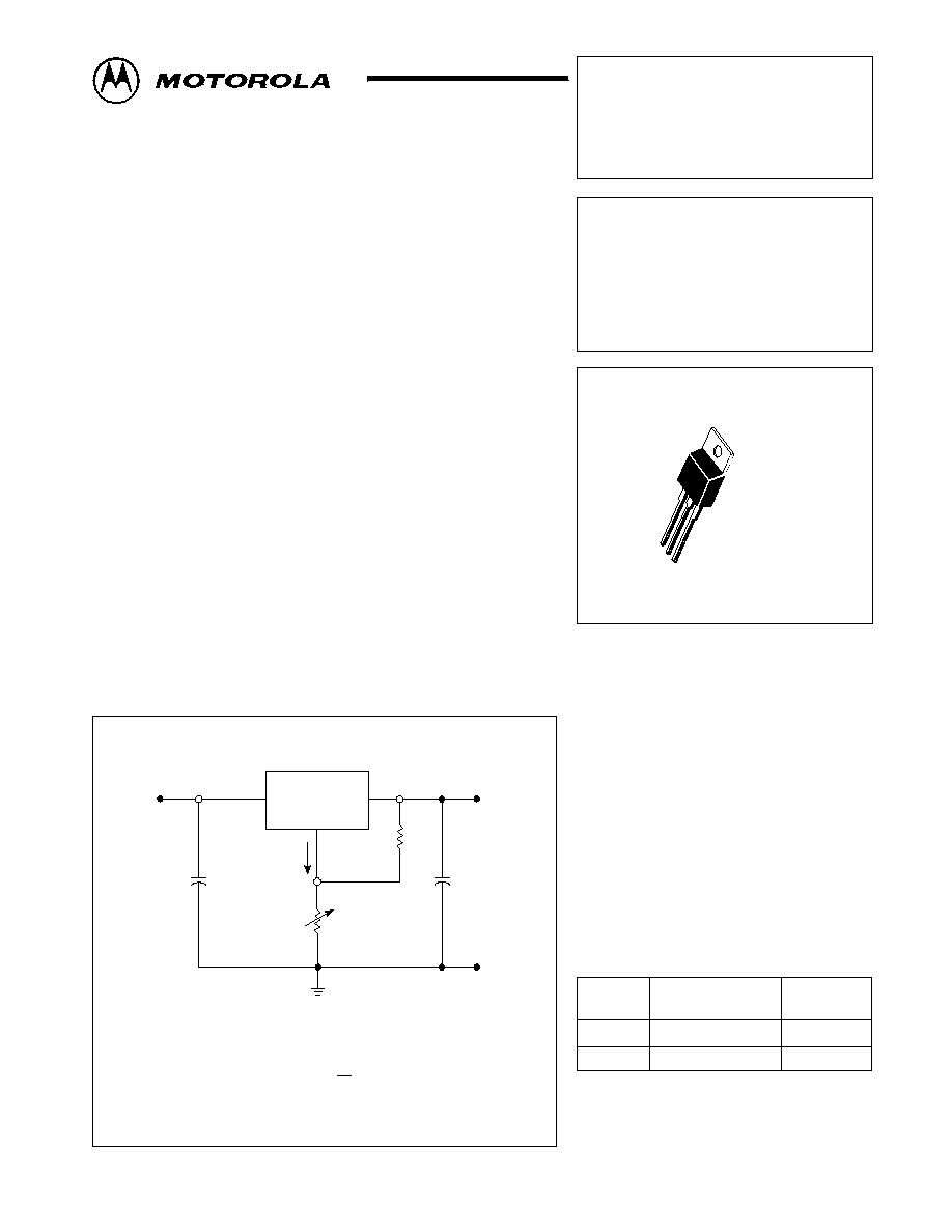
T SUFFIX
PLASTIC PACKAGE
CASE 221A
Pin 1.
Adjust
2. Vout
3. Vin
Heatsink surface is connected to Pin 2.
1
2
3
Device
Operating
Temperature Range
Package
LM350T
LM350BT#
Plastic Power
Plastic Power
TJ = 0
∞
to +125
∞
C
TJ = ≠40
∞
to +125
∞
C
# Automotive temperature range selections are
available with special test conditions and additional
tests. Contact your local Motorola sales office for
information.
1
MOTOROLA ANALOG IC DEVICE DATA
Three-Terminal Adjustable
Output Positive Voltage
Regulator
The LM350 is an adjustable three≠terminal positive voltage regulator
capable of supplying in excess of 3.0 A over an output voltage range of 1.2 V
to 33 V. This voltage regulator is exceptionally easy to use and requires only
two external resistors to set the output voltage. Further, it employs internal
current limiting, thermal shutdown and safe area compensation, making it
essentially blow≠out proof.
The LM350 serves a wide variety of applications including local, on card
regulation. This device also makes an especially simple adjustable switching
regulator, a programmable output regulator, or by connecting a fixed resistor
between the adjustment and output, the LM350 can be used as a precision
current regulator.
∑
Guaranteed 3.0 A Output Current
∑
Output Adjustable between 1.2 V and 33 V
∑
Load Regulation Typically 0.1%
∑
Line Regulation Typically 0.005%/V
∑
Internal Thermal Overload Protection
∑
Internal Short Circuit Current Limiting Constant with Temperature
∑
Output Transistor Safe Area Compensation
∑
Floating Operation for High Voltage Applications
∑
Standard 3≠lead Transistor Package
∑
Eliminates Stocking Many Fixed Voltages
Simplified Application
* = Cin is required if regulator is located an appreciable distance from power supply filter.
** = CO is not needed for stability, however, it does improve transient response.
Since IAdj is controlled to less than 100
µ
A, the error associated with
this term is negligible in most applications.
LM350
Vin
vout
R1
240
R2
Adjust
IAdj
Cin*
0.1
µ
F
+ CO**
1
µ
F
Vout
+
1.25 V 1
)
R2
R1
)
IAdj R2
©
Motorola, Inc. 1996
Rev 0

LM350
2
MOTOROLA ANALOG IC DEVICE DATA
MAXIMUM RATINGS
Rating
Symbol
Value
Unit
Input≠Output Voltage Differential
VI≠VO
35
Vdc
Power Dissipation
PD
Internally Limited
W
Operating Junction Temperature Range
TJ
≠ 40 to +125
∞
C
Storage Temperature Range
Tstg
≠ 65 to +150
∞
C
Soldering Lead Temperature (10 seconds)
Tsolder
300
∞
C
ELECTRICAL CHARACTERISTICS
(VI≠VO = 5.0 V; IL = 1.5 A; TJ = Tlow to Thigh; Pmax [Note 1], unless otherwise noted.)
Characteristics
Figure
Symbol
Min
Typ
Max
Unit
Line Regulation (Note 2)
TA = 25
∞
C, 3.0 V
VI≠VO
35 V
1
Regline
≠
0.0005
0.03
%/V
Load Regulation (Note 2)
TA = 25
∞
C, 10 mA
Il
3.0 A
VO
5.0 V
VO
5.0 V
2
Regload
≠
≠
5.0
0.1
25
0.5
mV
% VO
Thermal Regulation, Pulse = 20 ms,
(TA = +25
∞
C)
Regtherm
≠
0.002
≠
% VO/W
Adjustment Pin Current
3
IAdj
≠
50
100
µ
A
Adjustment Pin Current Change
3.0 V
VI≠VO
35 V
10 mA
IL
3.0 A, PD
Pmax
1,2
IAdj
≠
0.2
5.0
µ
A
Reference Voltage
3.0 V
VI≠VO
35 V
10 mA
IO
3.0 A, PD
Pmax
3
Vref
1.20
1.25
1.30
V
Line Regulation (Note 2)
3.0 V
VI≠VO
35 V
1
Regline
≠
0.02
0.07
%/V
Load Regulation (Note 2)
10 mA
IL
3.0 A
VO
5.0 V
VO
5.0 V
2
Regload
≠
≠
20
0.3
70
1.5
mV
% VO
Temperature Stability (Tlow
TJ
Thigh)
3
TS
≠
1.0
≠
% VO
Minimum Load Current to
Maintain Regulation (VI≠VO = 35 V)
3
ILmin
≠
3.5
10
mA
Maximum Output Current
VI≠VO
10 V, PD
Pmax
VI≠VO = 30 V, PD
Pmax, TA = 25
∞
C
3
Imax
3.0
0.25
4.5
1.0
≠
≠
A
RMS Noise, % of VO
TA= 25
∞
C, 10 Hz
f
10 kHz
N
≠
0.003
≠
% VO
Ripple Rejection, VO = 10 V, f = 120 Hz (Note 3)
Without CAdj
CAdj = 10
µ
F
4
RR
≠
66
65
80
≠
≠
dB
Long Term Stability, TJ = Thigh (Note 4)
TA= 25
∞
C for Endpoint Measurements
3
S
≠
0.3
1.0
%/1.0 k
Hrs.
Thermal Resistance, Junction≠to≠Case
Peak (Note 5)
Average (Note 6)
R
JC
≠
≠
2.3
≠
≠
1.5
∞
C/W
NOTES: 1. Tlow to Thigh = 0
∞
to +125
∞
C; Pmax = 25 W for LM350T; Tlow to Thigh = ≠ 40
∞
to +125
∞
C; Pmax = 25 W for LM350BT
2. Load and line regulation are specified at constant junction temperature. Changes in VO due to heating effects must be taken into account separately.
Pulse testing with low duty cycle is used.
3. CAdj, when used, is connected between the adjustment pin and ground.
4. Since Long≠Term Stability cannot be measured on each device before shipment, this specification is an engineering estimate of average stability
from lot to lot.
5. Thermal Resistance evaluated measuring the hottest temperature on the die using an infrared scanner. This method of evaluation yields very
accurate thermal resistance values which are conservative when compared to the other measurement techniques.
6. The average die temperature is used to derive the value of thermal resistance junction to case (average).
LM350
3
MOTOROLA ANALOG IC DEVICE DATA
Representative Schematic Diagram
310
310
230
120
5.6K
Vin
170
6.3V
160
12K
5.0pF
6.8K
13K
6.3V
105
4
0.45
Vout
Adjust
12.5K
2.4K
30
pF
30
pF
6.3V
125K
135
190
12.4K
3.6K
5.8K
11
0
5.1K
6.7K
510
200
* Pulse Testing Required:
1% Duty Cycle is suggested.
Line Regulation (%/V) =
VOH ≠ VOL
x 100
*
VCC
VIH
VIL
Vin
Vout
VOH
VOL
RL
+
1
µ
F
CO
240
1%
R1
Adjust
R2
1%
Cin
0.1
µ
F
LM350
IAdj
IL
Figure 1. Line Regulation and
IAdj/Line Test Circuit
VOL
LM350
4
MOTOROLA ANALOG IC DEVICE DATA
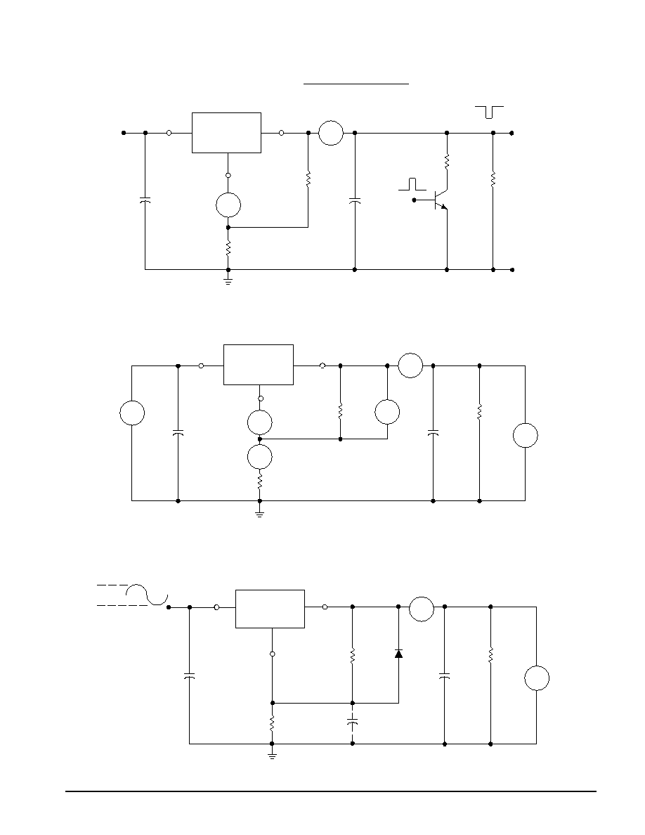
* Pulse Testing Required:
1% Duty Cycle is suggested.
Load Regulation (mV) = VO (min Load) ≠VO (max Load)
Load Regulation (% VO) =
VO (min Load) ≠ VO (max Load)
X 100
VO (min Load)
VO (max Load)
LM350
Cin
0.1
µ
F
Adjust
R2
1%
CO
1.0
µ
F
+
*
RL
(max Load)
RL
(min Load)
Vout
R1
240
1%
Vin
Vin
IAdj
IL
Figure 2. Load Regulation and
IAdj/Load Test Circuit
VO (min Load)
Pulse Testing Required:
1% Duty Cycle is suggested.
LM350
Vin
Vout
Adjust
R1
240
1%
+
1.0
µ
F
CO
RL
Cin
R2
1%
To Calculate R2:
Vout = ISET R2 + 1.250 V
Assume ISET = 5.25 mA
IL
IAdj
ISET
Vref
VO
VI
0.1
µ
F
Figure 3. Standard Test Circuit
LM350
Vin
Vout
Vout = 10 V
RL
Cin
0.1
µ
F
Adjust
R1
240
1%
D1 *
1N4002
CO
+
1.0
µ
F
24V
14V
R2
1.65K
1%
CAdj
10
µ
F
+
* D1 Discharges CAdj if Output is Shorted to Ground.
**CAdj provides an AC ground to the adjust pin.
f = 120 Hz
VO
IL
**
Figure 4. Ripple Rejection Test Circuit
LM350
5
MOTOROLA ANALOG IC DEVICE DATA
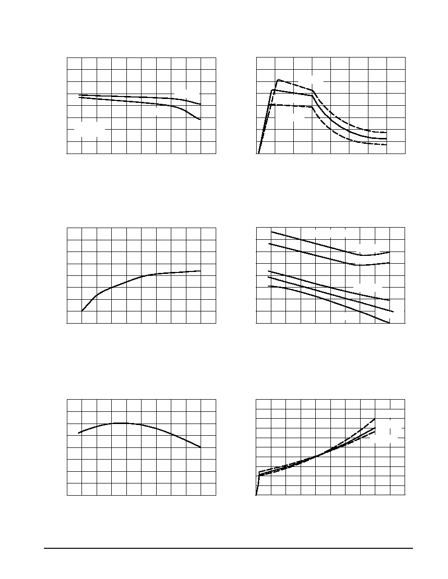
ref
V
,
REFERENCE VOL
T
AGE (V)
I B
, QUIESCENT
CURRENT
(mA)
I Adj
,
ADJUSTMENT
PIN CURRENT
(
A
)
µ
V
out
,
OUTPUT
VOL
T
AGE CHANGE (%)
Figure 5. Load Regulation
Figure 6. Current Limit
Figure 7. Adjustment Pin Current
Figure 8. Dropout Voltage
Figure 9. Temperature Stability
Figure 10. Minimum Operating Current
0.4
0.2
0
≠0.2
≠0.4
≠0.6
≠0.8
≠1.0
≠75
≠50
≠25
0
25
50
75
100
125
150
TJ, JUNCTION TEMPERATURE (
∞
C)
Vin = 15 V
Vout = 10 V
IL = 0.5 A
IL = 1.5 A
7
5
3
1
0
0
10
20
30
40
Vin≠Vout, INPUT VOLTAGE DIFFERENTIAL (Vdc)
I out
, OUTPUT
CURRENT
(A)
70
65
60
55
50
45
40
35
≠75
≠50
≠25
0
25
50
75
100
125
150
TJ, JUNCTION TEMPERATURE (
∞
C)
≠75
≠50
≠25
0
25
50
75
100
125
150
TJ, JUNCTION TEMPERATURE (
∞
C)
3.0
2.5
2.0
1.5
1.0
V0 = 100 mV
IL = 3.0 A
IL = 2.0 A
IL = 500 mA
IL = 200 mA
IL = 20 mA
≠75
≠50
≠25
0
25
50
75
100
125
150
TJ, JUNCTION TEMPERATURE (
∞
C)
1.260
1.250
1.240
1.230
1.220
5.0
4.5
4.0
3.5
3.0
2.5
2.0
1.5
1.0
0.5
0
0
10
20
30
40
Vin≠Vout, INPUT≠OUTPUT VOLTAGE DIFFERENTIAL (Vdc)
TJ = ≠55
∞
C
TJ = 25
∞
C
TJ = 150
∞
C
TJ = 55
∞
C
TJ = 150
∞
C
TJ = 25
∞
C
V
in
≠V
out
, INPUT≠OUTPUT
VOL
T
AGE
DIFFERENTIAL
(Vdc)