March 20, 1997 5:12 pm
Page 1 of 13
MC68302 Document
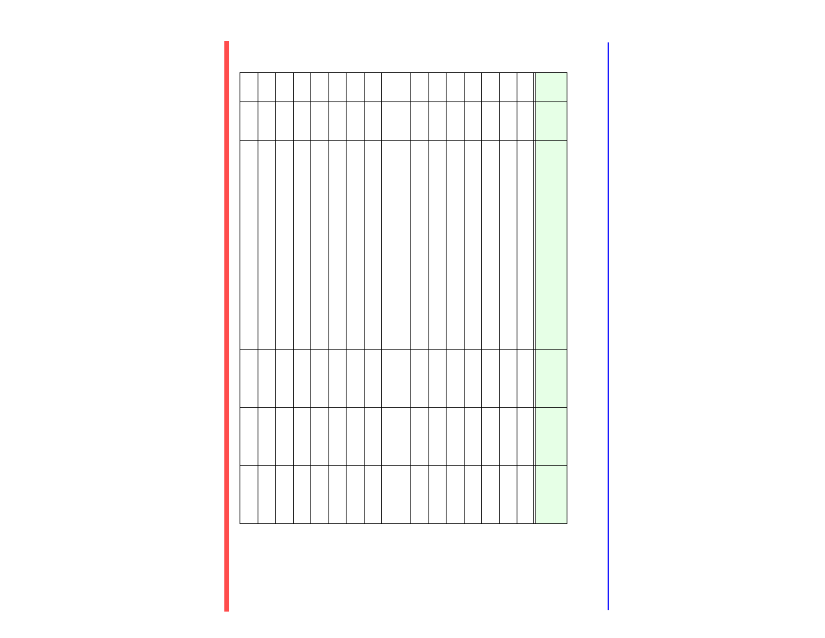
Table 1:
#
Spec
No.
Description
Spec Name
UM
33MHz
Min
33MHz
Max
1
1
Cycle period
tcyc
30
2
2,3
Clock pulse width
tcl,tch
15
3
5A
EXTAL to Clock delay
tcd
2
11
4
6
Clock high to FC, address valid
tchfcadv
0
27
5
7
Clock high to Address, Data Hi-z
tchadz
-
25
6
8
Clock high to Address, FC invalid (Minimum)
tchafi
0
-
7
9
Clock high to AS, DS asserted
tchsl
3
15
8
11
Address, FC Valid to AS, DS Assert (read)
AS assert (Write)
tafcvsl
8
-
9
12
Clock low to AS, DS negate
tclsn
-
15
10
13
AS, DS Negated to Address FC Invalid
tshafi
8
-
11
14
AS (and DS read) width asserted
tsl
60
-
12
14A
DS width asserted, write
tdsl
30
-
13
15
AS, DS width negate
tsh
30
-
14
16
Clock high to Control Bus Hi-z
tchca
-
25
15
17
AS, DS Negated to R/W Invalid
tshrh
8
-
16
18
Clock high to R/W hi
tchrh
-
15

March 20, 1997 5:12 pm
Page 2 of 13
MC68302 Document
17
20
Clock high to R/W lo
tchrl
-
15
18
20A
AS Asserted to R/W Low (Write)
tasrv
-
7
19
21
Address FC Valid to R/W Low (Write)
tafcvrl
8
-
20
22
R/W low to DS assert (write)
trasa
21
23
Clock low to data valid
tcldo
-
15
22
25
AS, DS Negated to Data-out invalid
tcldo
-
15
23
26
Data-out valid to DS Asserted (Write)
tdosl
8
-
24
27
Data in to Clock low
tdicl
4
-
25
28
AS, DS negate to DTACK negate
tshdah
0
65
26
29
AS, DS Negated to Data In invalid
tshdii
0
-
27
30
AS, DS negated to BERR negated
tshbeh
0
-
28
31
DTACK assert to Data-In valid
tdaldi
-
25
29
32
HALT,RESET in transition time
trhr, trhf
-
150
30
33
Clock high to BG assert
tchgl
-
15
31
34
Clock high to BG negate
tchgh
-
15
32
35
BR assert to BG assert
tbrlgl
2.5 clks
4.5 clks
33
36
BR negate to BG negate
tbrhgh
1.5 clks
2.5 clks
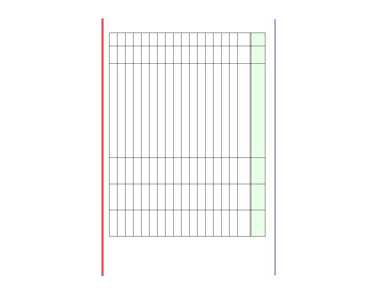
Table 1:
#
Spec
No.
Description
Spec Name
UM
33MHz
Min
33MHz
Max

March 20, 1997 5:12 pm
Page 3 of 13
MC68302 Document
34
37
BGACK assert to BG negate
tgalgh
2.5 clks
4.5 clks
35
37A
BGACK assert to BR negate
tgalbrh
10 ns
1.5 clks
36
38
BG assert to Addr, Data, etc. hi-z
tglz
-
25
37
39
BG width negate
tgh
1.5 clks
-
38
40
BGACK assert to Address valid
tgalav
15
-
39
41
BGACK assert to AS assert
tgalasa
-
20
40
44
AS, DS negate to AVEC negate
tshvph
0
25
41
46
BGACK width low
tgal
1.5 clks
1.5 clks
42
47
Async input setup time
tasi
7
-
43
48
BERR assert to DTACK assert
tbeldal
7
-
44
53
Data-out hold from clk high
tchdoi
0
-
45
55
R/W assert to Data bus impedance change
trldbd
0
-
46
56
HALT/RESET pulse width
thrpw
10 clks
-
47
57
BGACK negate to AS, DS, RW driven
tgasd
1.5 clks
-
48
57A
BGACK negate to FC
tgafd
1 clk
-
49
58
BR negate to AS, DS, RW driven
trhsd
1.5 clks
-
50
58A
BR negate to FC
trhfd
1 clk
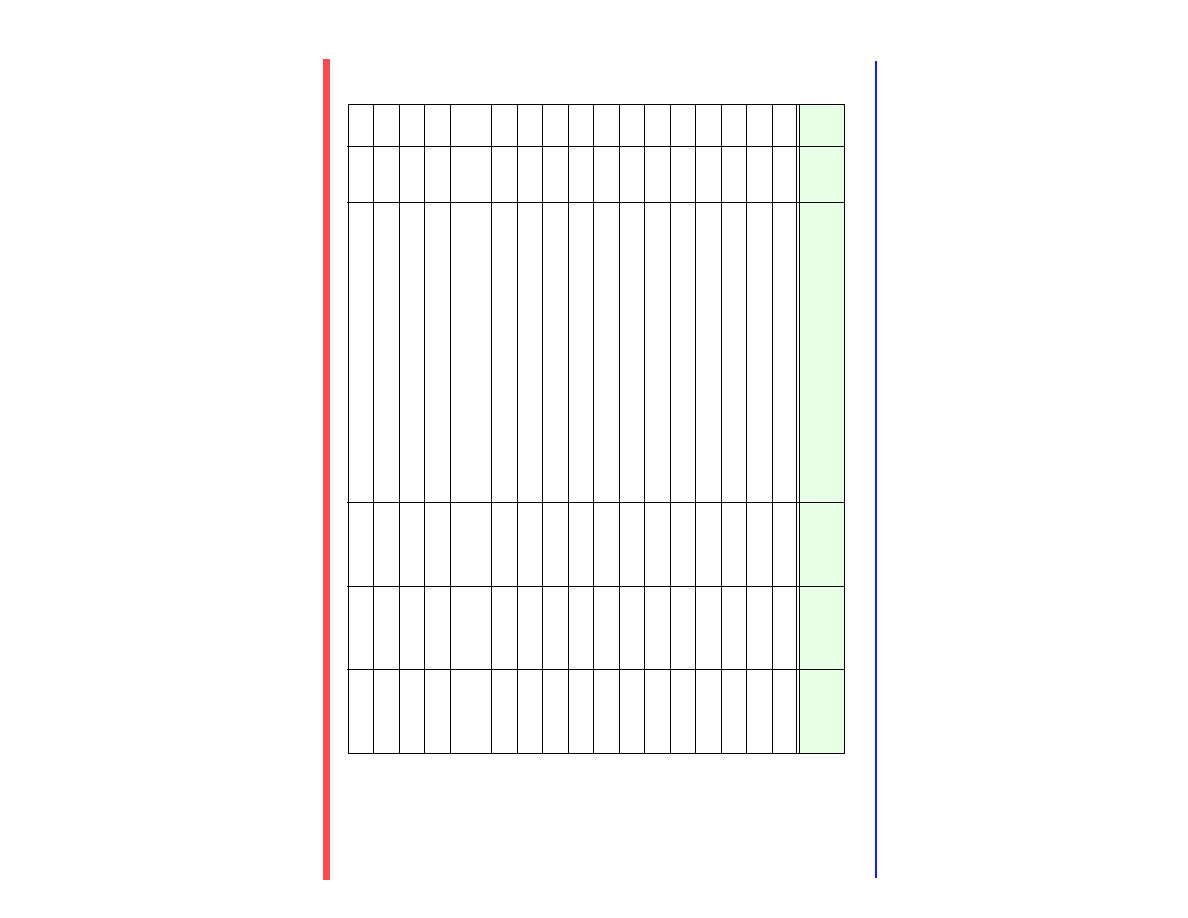
Table 1:
#
Spec
No.
Description
Spec Name
UM
33MHz
Min
33MHz
Max

March 20, 1997 5:12 pm
Page 4 of 13
MC68302 Document
51
60
Clock high to BCLR assert
tchbca
-
15
52
61
Clock high to BCLRO hi-z
tchbcn
-
15
53
62
Clock low to RMC assert
tclrml
-
17
54
63
Clock high to RMC negate
tchrmh
-
17
55
64
RMC negate to BG assert
trmhgl
-
15
56
80
DREQ asynchronous set up time
treqasi
10
-
57
81
DREQ width low
treql
2 clks
-
58
82
DREQ low to BR low
treqlbrl
-
2 clks
59
83
Clock high to BR low
tchbrl
-
15
60
84
Clock high to BR hi-z
tchbrz
-
15
61
85
BGACK low to BR hi-z
tbklbrz
15
-
62
86
Clock high to BGACK low
tchbkl
-
15
63
87
AS and BGACK high to BGACK low
tabhbkl
1.5 clks
2.5 clks +
20 ns
64
88
BG low to BGACK low
tbglbkl
1.5 clks
2.5 clks +
20 ns
65
89
BR hi-z to BG high
trhbgh
0
-
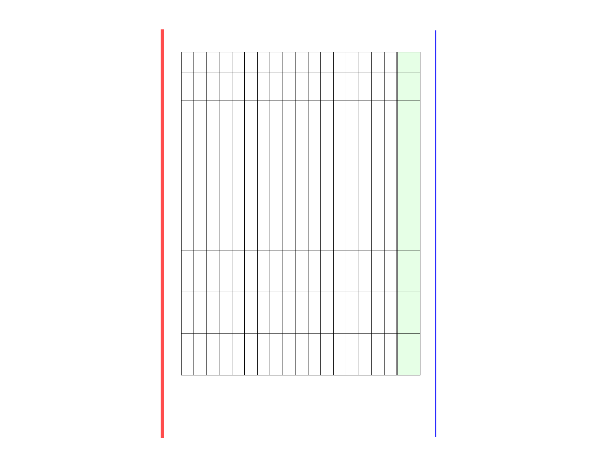
Table 1:
#
Spec
No.
Description
Spec Name
UM
33MHz
Min
33MHz
Max
March 20, 1997 5:12 pm
Page 5 of 13
MC68302 Document
66
90
Clock on which BGACK low to clock on
which AS low
tclbklal
2 clks
2 clks
67
91
Clock high to BGACK high
tchbkh
-
15
68
92
Clock low to BGACK hi-z
tclbkz
-
10
69
93
Clock high to DACK low
tchackl
-
15
70
94
Clock low to DACK high
tclackh
-
15
71
95
Clock high to DONE low (output)
tchdnl
-
15
72
96
Clock low to DONE hi-z
tcldnz
-
15
73
97
DONE input low to clock high
tdnltch
10
-
74
100
RW valid to DS low
trwvdsl
0
-
75
101
DS low to Data-in valid
tdsldiv
-
15
76
102
DTACK low to Data in hold time
tdkldh
0
-
77
103
AS valid to DS low
tasvdsl
0
-
78
104
DTACK low to AS, DS high
tdkldsh
0
-
79
105
DS high to DTACK high
tdshdkh
-
25
80
106
DS inactive to AS inactive
tdsiasi
0
-
81
107
DS high to RW high
tdshrwh
0
-
82
108
DS high to data hi-z
tdshdz
-
25
Table 1:
#
Spec
No.
Description
Spec Name
UM
33MHz
Min
33MHz
Max

March 20, 1997 5:12 pm
Page 6 of 13
MC68302 Document
83
108A
DS high to data out hold time
tdshdh
0
-
84
109A
Data out valid to DTACK low
tdovdkl
10
-
85
110
Address valid to AS low
tavasl
8
-
86
111
AS low to clock high
taslch
15
-
87
112
Clock low to AS high
tclash
-
25
88
113
AS high to address hold time on write
tashah
0
-
89
114
AS inactive time
tash
1 clk
-
90
115
UDS/LDS low to clock high
tslch
21
-
91
116
Clock low to UDS/LDS high
tclsh
-
20
92
117
RW valid to clock high
trwvch
15
-
93
118
Clock high to RW high
tchrwh
-
20
94
119
AS low to IAC high
tasliah
-
21
95
120
AS high to IAC low
tashial
-
21
96
121
AS low to DTACK low (0 wait states)
tasldtl
-
25
97
122
Clock low to DTACK low (1 wait state)
tcldtl
-
15
98
123
AS high to DTACK high
tashdth
-
20
99
124
DTACK high to DTACK hi-z
tdthdtz
-
10
Table 1:
#
Spec
No.
Description
Spec Name
UM
33MHz
Min
33MHz
Max

March 20, 1997 5:12 pm
Page 7 of 13
MC68302 Document
100
125
Clock high to data out valid
tchdov
-
15
101
126
AS high to data hi-z
tashdz
-
25
102
127
AS high to data out hold time
tashdoi
0
-
103
128
AS high to address hold time on read
tashai
0
-
104
129
UDS/LDS inactive time
tsh
1 clk
-
105
130
Data in valid to clock low
tcldiv
15
-
106
131
Clock low to data in hold time
tcldih
10
-
107
140
Clock high to IAC high
tchiah
-
21
108
141
Clock low to IAC low
tclial
21
109
142
Clock high to DTACK low
tchdtl
-
25
110
143
Clock low to DTACK high
tcldth
-
22
111
144
Clock high to data out valid
tchdov
-
15
112
145
AS high to data out hold time
tashdoh
0
-
113
150
Clock high to CS, IACK low
tchcsiakl
0
20
114
151
Clock low to CS, IACK high
tclcsiakh
0
20
115
152
CS width negated
tcsh
30
-
116
153
Clock high to DTACK low (0 wait states)
tchdtkl
-
25
Table 1:
#
Spec
No.
Description
Spec Name
UM
33MHz
Min
33MHz
Max

March 20, 1997 5:12 pm
Page 8 of 13
MC68302 Document
117
154
Clock low to DTACK low (1-6 wait states)
tcldtkh
-
15
118
155
Clock low to DTACK high
tcldtkh
-
20
119
156
Clock high to BERR low
tchberl
-
20
120
157
Clock low to BERR hi-z
tclberh
-
20
121
158
DTACK high to DTACK hi-z
tdtkhdtkz
-
10
122
160
AS low to CS low
taslcsl
-
16
123
161
AS high to CS high
tashcsh
-
16
124
162
Address valid to AS low
tavasl
8
-
125
163
RW valid to AS low
trwvasl
8
-
126
164
AS negated to address hold time
tashai
0
-
127
165
AS low to DTACK low (0 wait states)
tasldtkl
-
25
128
167
AS high to DTACK high
tashdtkh
-
18
129
168
AS low to BERR low
taslberl
-
18
130
169
AS high to BERR hi-z
tashberh
-
18
131
171
Input data hold time from S6 low
tidhcl
5
-
132
172
CS negated to data out invalid (write)
tcsndoi
7
-
133
173
Address, FC valid to CS asserted
tafvcsa
15
-
Table 1:
#
Spec
No.
Description
Spec Name
UM
33MHz
Min
33MHz
Max
March 20, 1997 5:12 pm
Page 9 of 13
MC68302 Document
134
174
CS negated to address, FC invalid
tcsnafi
12
-
135
175
CS low time (0 wait states)
tcslt
60
-
136
176
CS negate to RW invalid
tcsnrwi
7
-
137
177
CS assert to RW low (Write)
tcsarwl
-
8
138
178
CS negate to data in invalid
tcsndii
0
-
139
180
Input data setup time
tdsu
14
-
140
181
input data hold time
tdh
-
19
141
182
Clock high to data out valid
tchdov
-
20
142
190
Interrupt Pulse Width low IRQ
tipw
28
-
143
191
Minimum time between active edges
taemt
3 clks
-
144
200
Timer input capture pulse width
ttpw
28
-
145
201
TIN clock low pulse width
tticlt
28
-
146
202
TIN clock high pulse width and input capture high
pulse width
tticht
2 clks
-
147
203
TIN clock cycle time
tcyc
3 clks
-
148
204
Clock high to TOUT valid
tchtov
-
24
149
205
FRZ input setup time (to clock high)
tfrzsu
14
-
150
206
FRZ input setup time (from clock high)
tfrzht
7
-
Table 1:
#
Spec
No.
Description
Spec Name
UM
33MHz
Min
33MHz
Max
March 20, 1997 5:12 pm
Page 10 of 13
MC68302 Document
151
250
SPCLK clock output period
4 clks
64 clks
152
251
SPCLK clock output rise/fall time
0
6
153
252
Delay from SPCLK to transmit
0
20
154
253
SCP receive setup time
20
-
155
254
SCP receive hold time
6
-
156
260
L1CLK (IDL Clock) frequency
-
13.3 MHz
157
261
L1CLK width low
28
-
158
262
L1CLK width high
P+10
-
159
263
L1TXD, L1RQ, SDS1-SDS2 rise/fall time
-
12
160
264
L1SY1 (sync) setup time (to L1CLK falling edge)
15
-
161
265
L1SY1 (sync) hold time (to L1CLK falling edge)
28
-
162
266
L1SY1 (sync) inactive before 4th L1CLK
0
-
163
267
L1TXD active delay (from L1CLK falling edge)
0
40
164
268
L1TXD to hi-z (from L1CLK rising edge)
0
26
165
269
L1RXD setup time (to L1CLK falling edge)
26
-
166
270
L1RXD hold time (from L1CLK falling edge)
26
-
167
271
Time between successive IDL syncs
20 L1CLKS
-
Table 1:
#
Spec
No.
Description
Spec Name
UM
33MHz
Min
33MHz
Max
March 20, 1997 5:12 pm
Page 11 of 13
MC68302 Document
168
272
L1RQ valid before falling edge of L1SY1
1 L1CLKS
-
169
273
L1GR setup time (to L1SY1 falling edge)
26
-
170
274
L1GR hold time (from L1SY1 falling edge)
26
-
171
275
SDS1-SDS2 active delay from L1CLK rising edge
7
40
172
276
SDS1-SDS2 inactive delay from L1CLK falling
edge
7
40
173
280
L1CLK clock period normal mode
1800
2100
174
281
L1CLK width low/high normal mode
840
1450
175
282
L1CLK rise/fall time Normal mode
-
-
176
280
L1CLK clock period MUX mode
150
-
177
281
L1CLK width low/high MUX mode
55
-
178
281A
L1CLK width high MUX mode
P+10
-
179
282
L1CLK rise/fall time MUX mode
-
-
180
283
L1SY1 sync setup time to L1CLK falling edge
15
-
181
284
L1SY1 sync hold time (from L1CLK falling edge)
26
-
182
285
L1TxD active delay (from L1ClK rising edge)
0
55
183
286
L1TXD active delay (from L1SY1 rising edge)
0
55
184
287
L1RXD Setup time to L1CLK rising edge
14
-
Table 1:
#
Spec
No.
Description
Spec Name
UM
33MHz
Min
33MHz
Max
March 20, 1997 5:12 pm
Page 12 of 13
MC68302 Document
185
288
L1RXD hold time from L1CLK rising edge
26
-
186
289
Time between successive L1SY1
64 L1CLK
192 L1CLK
-
-
187
290
SDS1-SDS2 active delay from L1CLK rising edge
7
45
188
291
SDS1-SDS2 active delay from L1SY1 rising edge
7
45
189
292
SDS1-SDS2 inactive delay from L1CLK falling
edge
7
45
190
293
GCIDCL (GCI data clock) active delay
0
26
191
300
L1CLK (PCM clock) frequency
-
13.2 MHz
192
301
L1CLK width low
27
-
193
301A
L1CLK width high
P+10
-
194
302
L1SY0-L1SY1 setup time
0
-
195
303
L1SY0-L1SY1 hold time
20
-
196
304
L1SY0-L1SY1 width low
1 L1CLK
-
197
305
Time between successive sync signals
8 L1CLK
-
198
306
L1TXD data valid after L1CLK rising edge
0
40
199
307
L1TXD to hi-z (from L1CLK rising edge)
0
26
200
308
L1RXD setup time (to L1CLK falling edge)
11
-
Table 1:
#
Spec
No.
Description
Spec Name
UM
33MHz
Min
33MHz
Max
March 20, 1997 5:12 pm
Page 13 of 13
MC68302 Document
201
309
L1RXD hold time (from L1CLK falling edge)
26
-
202
315
RCLK1 and TCLK1 frequency
Internal clk
External clk
-
-
11 MHz
13.2 MHz
203
316
RCLK1 and TCLK1 low
Internal clk
External clk
35ns
P+10
-
-
204
316A
RCLK1 and TCLK1 high
Internal clk
External clk
35
25
-
-
205
317
RCLK1 and TCLK1 rise/fall time
Internal clk
External clk
-
-
11
-
206
318
RXD1 active delay from TCLK1 falling edge
Internal clk
External clk
0
0
20
30
207
319
RTS1 active/inactive delay from TCLK1 falling
edge
Internal clk
External clk
0
0
20
50
208
320
CTS1 setup time to TCLK1 rising edge
Internal clk
External clk
30
7
-
-
209
321
RXD1 setup time to RCLK1 rising edge
Internal clk
External clk
30
7
-
-
210
322
RXD1 hold time from RCLK1 rising edge
Internal clk
External clk
7
30
-
-
211
323
CD1 setup time to RCLK1 rising edge
Internal clk
External clk
30
7
-
-
Table 1:
#
Spec
No.
Description
Spec Name
UM
33MHz
Min
33MHz
Max