Äîêóìåíòàöèÿ è îïèñàíèÿ www.docs.chipfind.ru
1
Rectifier Device Data
Designer's
TM
Data Sheet
SWITCHMODE
TM
Power Rectifier
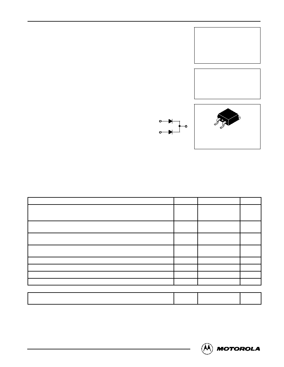
D2PAK Surface Mount Power Package
The D2PAK Power Rectifier employs the use of the Schottky Barrier principle
with a platinum barrier metal. These stateoftheart devices have the
following features:
·
Package Designed for Power Surface Mount Applications
·
CenterTap Configuration
·
Guardring for Stress Protection
·
Low Forward Voltage
·
150
°
C Operating Junction Temperature
·
Epoxy Meets UL94, VO at 1/8
·
Guaranteed Reverse Avalanche
·
Short Heat Sink Tab Manufactured -- Not Sheared!
·
Similar in Size to Industry Standard TO220 Package
Mechanical Characteristics
·
Case: Epoxy, Molded
·
Weight: 1.7 grams (approximately)
·
Finish: All External Surfaces Corrosion Resistant and Terminal Leads are
Readily Solderable
·
Lead and Mounting Surface Temperature for Soldering Purposes:
260
°
C Max. for 10 Seconds
·
Shipped 50 units per plastic tube
·
Available in 24 mm Tape and Reel, 800 units per 13
reel by adding a "T4"
suffix to the part number
·
Marking: B20100T
MAXIMUM RATINGS, PER LEG
Rating
Symbol
Value
Unit
Peak Repetitive Reverse Voltage
Working Peak Reverse Voltage
DC Blocking Voltage
VRRM
VRWM
VR
100
Volts
Average Rectified Forward Current
(Rated VR) TC = 110
°
C
Total Device
IF(AV)
10
20
Amps
Peak Repetitive Forward Current
(Rated VR, Square Wave, 20 kHz), TC = 100
°
C
IFRM
20
Amps
Non-repetitive Peak Surge Current
(Surge applied at rated load conditions halfwave, single phase, 60 Hz)
IFSM
150
Amps
Peak Repetitive Reverse Surge Current (2.0
µ
s, 1.0 kHz)
IRRM
0.5
Amp
Storage Temperature
Tstg
65 to +175
°
C
Operating Junction Temperature
TJ
65 to +150
°
C
Voltage Rate of Change (Rated VR)
dv/dt
10000
V/
µ
s
THERMAL CHARACTERISTICS, PER LEG
Thermal Resistance -- Junction to Case
-- Junction to Ambient (1)
R
JC
R
JA
2.0
50
°
C/W
(1) See Chapter 7 for mounting conditions
Designer's Data for "Worst Case" Conditions -- The Designer's Data Sheet permits the design of most circuits entirely from the information presented. SOA Limit
curves -- representing boundaries on device characteristics -- are given to facilitate "worst case" design.
Designer's and SWITCHMODE are trademarks of Motorola, Inc.
Thermal Clad is a trademark of the Bergquist Company
Preferred devices are Motorola recommended choices for future use and best overall value.
Order this document
by MBRB20100CT/D
MOTOROLA
SEMICONDUCTOR TECHNICAL DATA
©
Motorola, Inc. 1996
MBRB20100CT
SCHOTTKY BARRIER
RECTIFIER
20 AMPERES
100 VOLTS
CASE 418B02
D2PAK
Motorola Preferred Device
4
3
1
1
3
4
Rev 1
MBRB20100CT
2
Rectifier Device Data
ELECTRICAL CHARACTERISTICS, PER LEG
Rating
Symbol
Value
Unit
Maximum Instantaneous Forward Voltage (2)
(iF = 10 Amp, TC = 125
°
C)
(iF = 10 Amp, TC = 25
°
C)
(iF = 20 Amp, TC = 125
°
C)
(iF = 20 Amp, TC = 25
°
C)
vF
0.75
0.85
0.85
0.95
Volts
Maximum Instantaneous Reverse Current (2)
(Rated dc Voltage, TJ = 125
°
C)
(Rated dc Voltage, TJ = 25
°
C)
iR
6.0
0.1
mA
(2) Pulse Test: Pulse Width = 300
µ
s, Duty Cycle
2.0%.
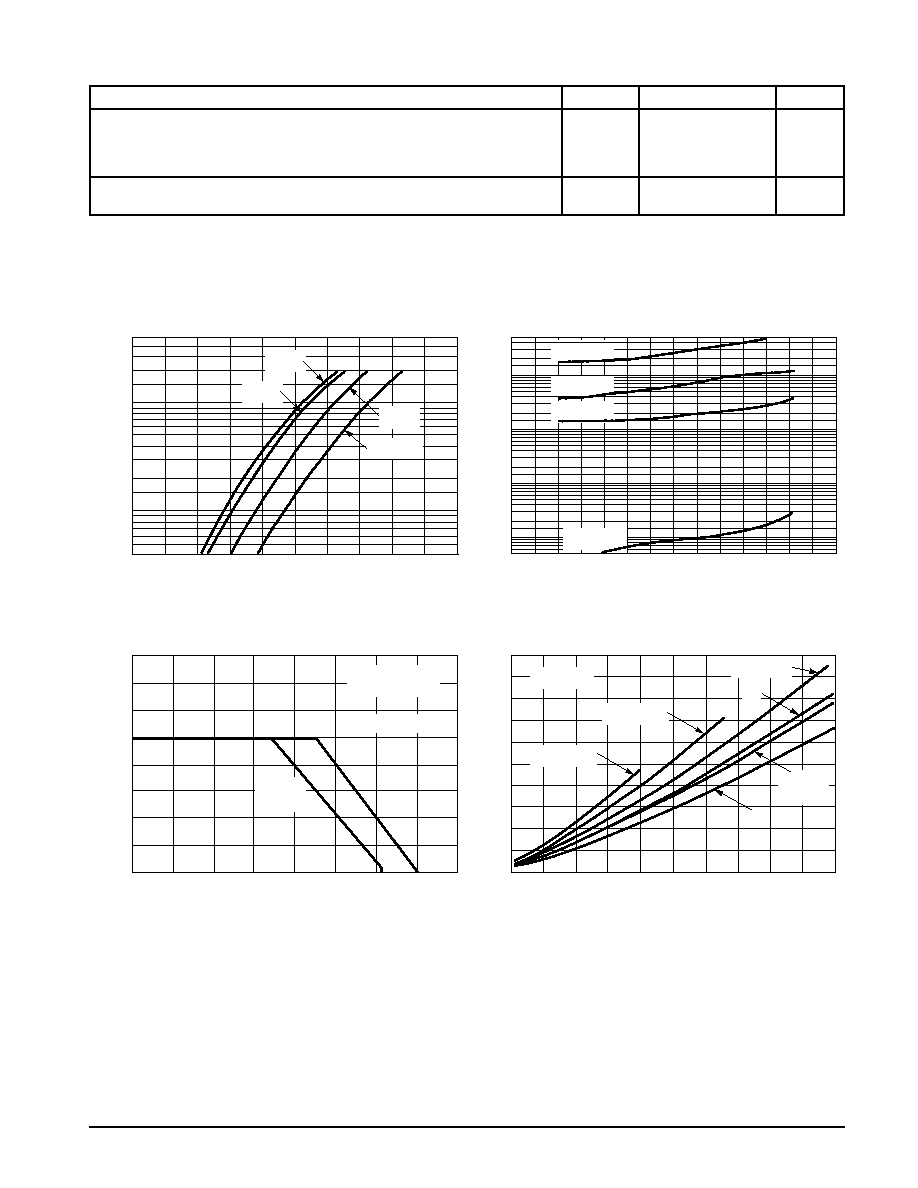
Figure 1. Typical Forward Voltage Per Diode
Figure 2. Typical Reverse Current Per Diode
Figure 3. Typical Current Derating, Case,
Per Leg
0.01
0.1
1
10
120
100
80
60
40
20
0
VR, REVERSE VOLTAGE (VOLTS)
I R
, REVERSE CURRENT
(mA)
TJ = 150
°
C
TJ = 125
°
C
TJ = 100
°
C
TJ = 25
°
C
0.5
0
vF, INSTANTANEOUS VOLTAGE (VOLTS)
1
3
5
10
20
50
0.1
0.2
0.3
0.4
0.5
0.6
0.7
0.8
0.9
1
i F
, INST
ANT
ANEOUS
FOR
W
ARD
CURRENT
(AMPS)
TJ = 25
°
C
100
°
C
150
°
C
175
°
C
0
AVERAGE CURRENT (AMPS)
0
2
4
6
8
10
12
14
16
18
20
2
4
6
8
10
12
14
16
18
20
A
VERAGE POWER (W
A
TTS)
TJ = 125
°
C
DC
IPK/IAV = 10
IPK/IAV = 20
PI
IPK/IAV = 5
32
80
TC, CASE TEMPERATURE (
°
C)
28
24
20
16
12
8
4
0
90
100
110
120
130
I F(A
V)
, A
VERAGE
FOR
W
ARD
CURRENT
(AMPS)
DC
RATED VOLTAGE
APPLIED
SQUARE
WAVE
R
JC = 2
°
C/W
140
150
160
SQUARE
WAVE
Figure 4. Average Power Dissipation and
Average Current
MBRB20100CT
3
Rectifier Device Data
INFORMATION FOR USING THE D2PAK SURFACE MOUNT PACKAGE
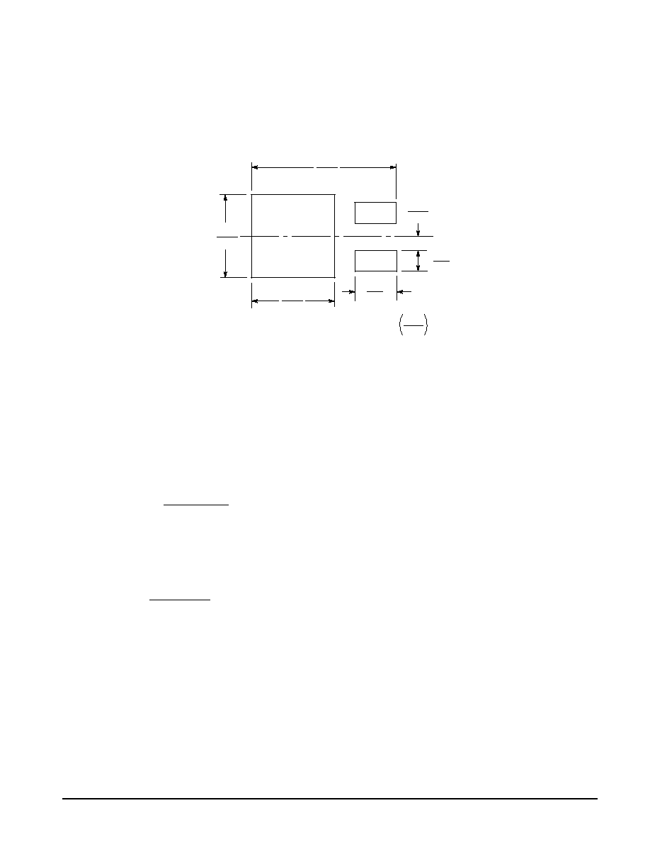
MINIMUM RECOMMENDED FOOTPRINT FOR SURFACE MOUNTED APPLICATIONS
Surface mount board layout is a critical portion of the total
design. The footprint for the semiconductor packages must be
the correct size to insure proper solder connection interface
between the board and the package. With the correct pad
geometry, the packages will self align when subjected to a
solder reflow process.
mm
inches
0.74
18.79
0.065
1.651
0.07
1.78
0.14
3.56
0.330
8.38
0.420
10.66
D2PAK POWER DISSIPATION
The power dissipation of the D2PAK is a function of the drain
pad size. This can vary from the minimum pad size for
soldering to a pad size given for maximum power dissipation.
Power dissipation for a surface mount device is determined by
TJ(max), the maximum rated junction temperature of the die,
R
JA, the thermal resistance from the device junction to
ambient; and the operating temperature, TA. Using the values
provided on the data sheet for the D2PAK package, PD can be
calculated as follows:
PD =
TJ(max) TA
R
JA
The values for the equation are found in the maximum
ratings table on the data sheet. Substituting these values into
the equation for an ambient temperature TA of 25
°
C, one can
calculate the power dissipation of the device which in this case
is 2.5 watts.
PD =
150
°
C 25
°
C
50
°
C/W
= 2.5 watts
The 50
°
C/W for the D2PAK package assumes the use of the
recommended footprint on a glass epoxy printed circuit board
to achieve a power dissipation of 2.5 watts. There are other
alternatives to achieving higher power dissipation from the
D2PAK package. One is to increase the area of the drain pad.
By increasing the area of the drain pad, the power dissipation
can be increased. Although one can almost double the power
dissipation with this method, one will be giving up area on the
printed circuit board which can defeat the purpose of using
surface mount technology.
Another alternative would be to use a ceramic substrate or
an aluminum core board such as Thermal Clad
TM
. Using a
board material such as Thermal Clad, an aluminum core
board, the power dissipation can be doubled using the same
footprint.
MBRB20100CT
4
Rectifier Device Data
SOLDERING PRECAUTIONS
The melting temperature of solder is higher than the rated
temperature of the device. When the entire device is heated
to a high temperature, failure to complete soldering within a
short time could result in device failure. Therefore, the
following items should always be observed in order to
minimize the thermal stress to which the devices are
subjected.
·
Always preheat the device.
·
The delta temperature between the preheat and soldering
should be 100
°
C or less.*
·
When preheating and soldering, the temperature of the
leads and the case must not exceed the maximum
temperature ratings as shown on the data sheet. When
using infrared heating with the reflow soldering method,
the difference shall be a maximum of 10
°
C.
·
The soldering temperature and time shall not exceed
260
°
C for more than 5 seconds.
·
When shifting from preheating to soldering, the maximum
temperature gradient shall be 5
°
C or less.
·
After soldering has been completed, the device should be
allowed to cool naturally for at least three minutes.
Gradual cooling should be used as the use of forced
cooling will increase the temperature gradient and result
in latent failure due to mechanical stress.
·
Mechanical stress or shock should not be applied during
cooling.
* Soldering a device without preheating can cause excessive
thermal shock and stress which can result in damage to the
device.
* Due to shadowing and the inability to set the wave height to
incorporate other surface mount components, the D2PAK is
not recommended for wave soldering.
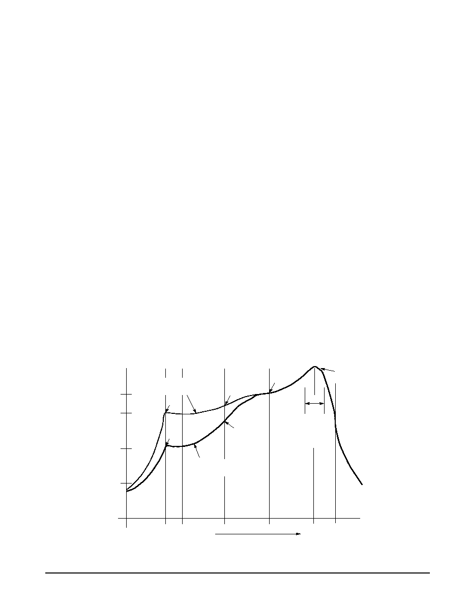
TYPICAL SOLDER HEATING PROFILE
For any given circuit board, there will be a group of control
settings that will give the desired heat pattern. The operator
must set temperatures for several heating zones, and a figure
for belt speed. Taken together, these control settings make up
a heating "profile" for that particular circuit board. On
machines controlled by a computer, the computer remembers
these profiles from one operating session to the next. Figure
5 shows a typical heating profile for use when soldering the
D2PAK to a printed circuit board. This profile will vary among
soldering systems but it is a good starting point. Factors that
can affect the profile include the type of soldering system in
use, density and types of components on the board, type of
solder used, and the type of board or substrate material being
used. This profile shows temperature versus time. The line on
the graph shows the actual temperature that might be
experienced on the surface of a test board at or near a central
solder joint. The two profiles are based on a high density and
a low density board. The Vitronics SMD310 convection/in-
frared reflow soldering system was used to generate this
profile. The type of solder used was 62/36/2 Tin Lead Silver
with a melting point between 177 189
°
C. When this type of
furnace is used for solder reflow work, the circuit boards and
solder joints tend to heat first. The components on the board
are then heated by conduction. The circuit board, because it
has a large surface area, absorbs the thermal energy more
efficiently, then distributes this energy to the components.
Because of this effect, the main body of a component may be
up to 30 degrees cooler than the adjacent solder joints.
STEP 1
PREHEAT
ZONE 1
"RAMP"
STEP 2
VENT
"SOAK"
STEP 3
HEATING
ZONES 2 & 5
"RAMP"
STEP 4
HEATING
ZONES 3 & 6
"SOAK"
STEP 5
HEATING
ZONES 4 & 7
"SPIKE"
STEP 6
VENT
STEP 7
COOLING
200
°
C
150
°
C
100
°
C
50
°
C
TIME (3 TO 7 MINUTES TOTAL)
TMAX
SOLDER IS LIQUID FOR
40 TO 80 SECONDS
(DEPENDING ON
MASS OF ASSEMBLY)
205
°
TO 219
°
C
PEAK AT
SOLDER JOINT
DESIRED CURVE FOR LOW
MASS ASSEMBLIES
DESIRED CURVE FOR HIGH
MASS ASSEMBLIES
100
°
C
150
°
C
160
°
C
170
°
C
140
°
C
Figure 5. Typical Solder Heating Profile for D2PAK
MBRB20100CT
5
Rectifier Device Data
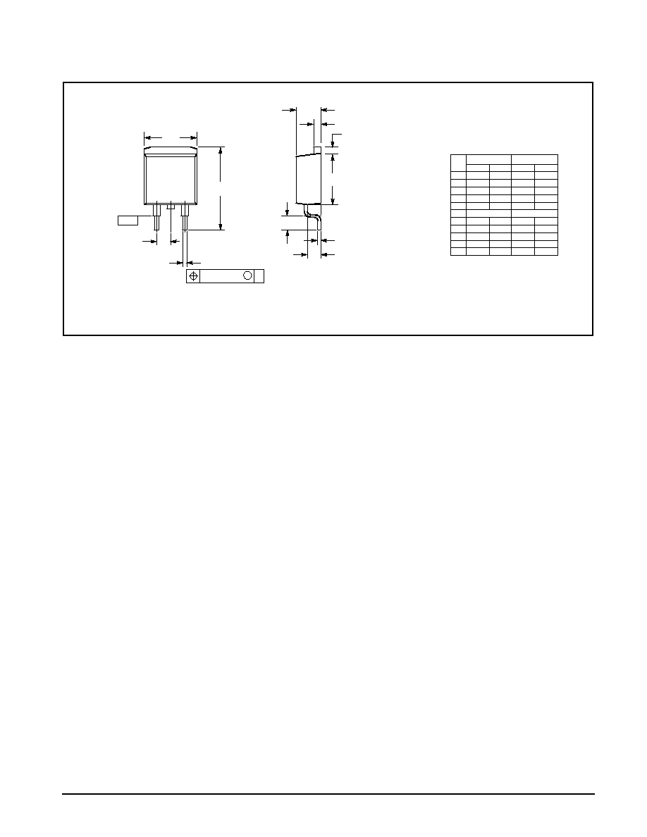
PACKAGE DIMENSIONS
NOTES:
1. DIMENSIONING AND TOLERANCING PER ANSI
Y14.5M, 1982.
2. CONTROLLING DIMENSION: INCH.
DIM
MIN
MAX
MIN
MAX
MILLIMETERS
INCHES
A
0.340
0.380
8.64
9.65
B
0.380
0.405
9.65
10.29
C
0.160
0.190
4.06
4.83
D
0.020
0.035
0.51
0.89
E
0.045
0.055
1.14
1.40
G
0.100 BSC
2.54 BSC
H
0.080
0.110
2.03
2.79
J
0.018
0.025
0.46
0.64
K
0.090
0.110
2.29
2.79
S
0.575
0.625
14.60
15.88
V
0.045
0.055
1.14
1.40
STYLE 3:
PIN 1. ANODE
2. CATHODE
3. ANODE
4. CATHODE
CASE 418B02
ISSUE B
SEATING
PLANE
B
S
G
D
T
M
0.13 (0.005)
T
2
3
1
4
3 PL
K
J
H
V
E
C
A