MOTOROLA
SEMICONDUCTOR TECHNICAL DATA
1
REV 0.1
©
Motorola, Inc. 1997
2/97
Product Preview
Low-Voltage 1:10 Differential
ECL/PECL Clock Driver
The MC100EP111 is a low skew 1≠to≠10 differential driver, designed
with clock distribution in mind. It accepts two clock sources into an input
multiplexer. The input signals can be either differential or single≠ended if
the VBB output is used. The selected signal is fanned out to 10 identical
differential outputs.
∑
100ps Part≠to≠Part Skew
∑
35ps Output≠to≠Output Skew
∑
Differential Design
∑
VBB Output
∑
Voltage and Temperature Compensated Outputs
∑
Low Voltage VEE Range of ≠2.375 to ≠3.8V
∑
75k
Input Pulldown Resistors
The EP111 is specifically designed, modeled and produced with low
skew as the key goal. Optimal design and layout serve to minimize gate≠
to≠gate skew within a device, and empirical modeling is used to
determine process control limits that ensure consistent tpd distributions
from lot to lot. The net result is a dependable, guaranteed low skew
device.
To ensure that the tight skew specification is met it is necessary that
both sides of the differential output are terminated into 50
, even if only
one side is being used. In most applications, all ten differential pairs will
be used and therefore terminated. In the case where fewer than ten pairs
are used, it is necessary to terminate at least the output pairs on the same
package side as the pair(s) being used on that side, in order to maintain
minimum skew. Failure to do this will result in small degradations of
propagation delay (on the order of 10≠20ps) of the output(s) being used
which, while not being catastrophic to most designs, will mean a loss of
skew margin.
The MC100EP111, as with most other ECL devices, can be operated from a positive VCC supply in PECL mode. This allows
the EP111 to be used for high performance clock distribution in +3.3V or +2.5V systems. Designers can take advantage of the
EP111's performance to distribute low skew clocks across the backplane or the board. In a PECL environment, series or
Thevenin line terminations are typically used as they require no additional power supplies. For more information on using PECL,
designers should refer to Motorola Application Note AN1406/D.
This document contains information on a product under development. Motorola reserves the right to change or
discontinue this product without notice.
MC100EP111
LOW≠VOLTAGE
1:10 DIFFERENTIAL
ECL/PECL CLOCK DRIVER
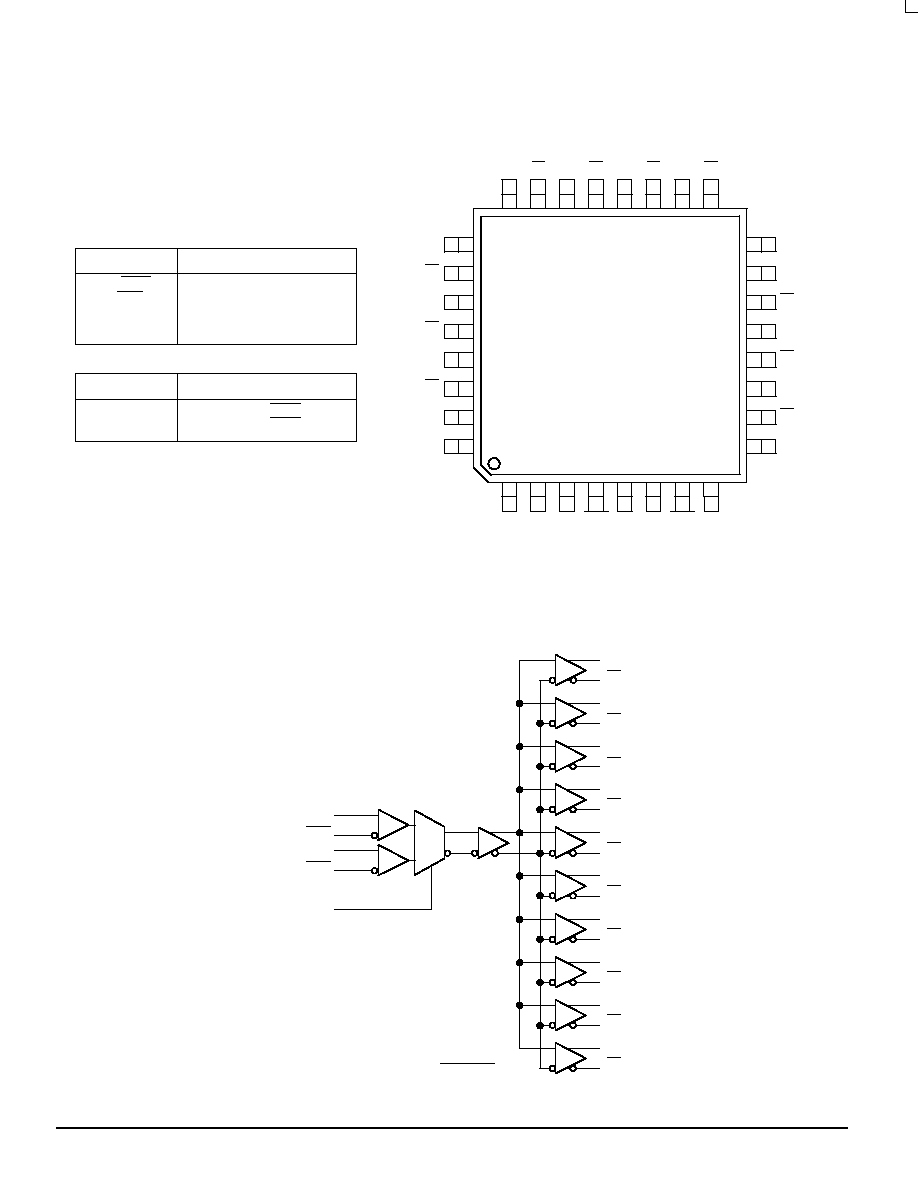
FA SUFFIX
32≠LEAD TQFP PACKAGE
CASE 873A≠02
MC100EP111
MOTOROLA
TIMING SOLUTIONS
BR1333 -- Rev 6
2
VCCO
PIN NAMES
Function
Differential Input Pairs
Differential Outputs
Active Clock Select Input
VBB Output
Pins
CLKn, CLKn
Q0:9, Q0:9
CLK_SEL
VBB
CLK_SEL
25
26
27
28
29
30
31
32
15
14
13
12
11
10
9
1
2
3
4
5
6
7
8
24
23
22
21
20
19
18
17
16
MC100EP111
Q9
Q9
Q8
Q8
Q7
Q7
VCCO
VCCO
Q0
Q0
Q1
Q1
Q2
Q2
VCCO
VEE
CLK1
CLK1
VBB
CLK0
CLK0
VCC
Q6
Q6
Q5
Q5
Q4
Q4
Q3
Q3
FUNCTION
Active Input
CLK0, CLK0
CLK1, CLK1
CLK_SEL
0
1
LOGIC SYMBOL
Q0
Q0
Q1
Q1
Q2
Q2
Q3
Q3
Q4
Q4
Q5
Q5
Q6
Q6
Q7
Q7
Q8
Q8
VBB
Q9
Q9
0
1
CLK0
CLK0
CLK1
CLK1
CLK_SEL
Pinout: 32≠Lead TQFP
(Top View)

MC100EP111
TIMING SOLUTIONS
BR1333 -- Rev 6
3
MOTOROLA
ECL DC CHARACTERISTICS
≠40
∞
C
0
∞
C
25
∞
C
85
∞
C
Symbol
Characteristic
Min
Typ
Max
Min
Typ
Max
Min
Typ
Max
Min
Typ
Max
Unit
VOH
Output HIGH Voltage
≠1.025
≠0.955
≠0.880
≠1.025
≠0.955
≠0.880
≠1.025
≠0.955
≠0.880
≠1.025
≠0.955
≠0.880
V
VOL
Output LOW Voltage
≠1.810
≠1.705
≠1.620
≠1.810
≠1.705
≠1.620
≠1.810
≠1.705
≠1.620
≠1.810
≠1.705
≠1.620
V
VIH
Input HIGH Voltage
≠1.165
≠0.880
≠1.165
≠0.880
≠1.165
≠0.880
≠1.165
≠0.880
V
VIL
Input LOW Voltage
≠1.810
≠1.475
≠1.810
≠1.475
≠1.810
≠1.475
≠1.810
≠1.475
V
VBB
Output Reference
Voltage
≠1.38
≠1.26
≠1.38
≠1.26
≠1.38
≠1.26
≠1.38
≠1.26
V
VEE
Power Supply Voltage
≠2.375
≠3.8
≠2.375
≠3.8
≠2.375
≠3.8
≠2.375
≠3.8
V
IIH
Input HIGH Current
150
150
150
150
µ
A
IEE
Power Supply Current
mA
PECL DC CHARACTERISTICS
≠40
∞
C
0
∞
C
25
∞
C
85
∞
C
Symbol
Characteristic
Min
Typ
Max
Min
Typ
Max
Min
Typ
Max
Min
Typ
Max
Unit
VOH
Output HIGH Voltage
(1.)
2.275
2.345
2.420
2.275
2.345
2.420
2.275
2.345
2.420
2.275
2.345
2.420
V
VOL
Output LOW Voltage
(1.)
1.490
1.595
1.680
1.490
1.595
1.680
1.490
1.595
1.680
1.490
1.595
1.680
V
VIH
Input HIGH Voltage
(1.)
2.135
2.420
2.135
2.420
2.135
2.420
2.135
2.420
V
VIL
Input LOW Voltage
(1.)
1.490
1.825
1.490
1.825
1.490
1.825
1.490
1.825
V
VBB
Output Reference
Voltage (Note 1.)
1.92
2.04
1.92
2.04
1.92
2.04
1.92
2.04
V
VCC
Power Supply Voltage
2.375
3.8
2.375
3.8
2.375
3.8
2.375
3.8
V
IIH
Input HIGH Current
150
150
150
150
µ
A
IEE
Power Supply Current
mA
1. These values are for VCC = 3.3V. Level Specifications will vary 1:1 with VCC.
AC CHARACTERISTICS (VEE = VEE (min) to VEE (max); VCC = VCCO = GND)
≠40
∞
C
0
∞
C
25
∞
C
85
∞
C
Symbol
Characteristic
Min
Typ
Max
Min
Typ
Max
Min
Typ
Max
Min
Typ
Max
Unit
Condition
tPLH
tPHL
Propagation Delay to Output
IN (differential)
IN (single≠ended)
400
400
ps
tskew
Within≠Device Skew
Part≠to≠Part Skew (Diff)
35
100
35
100
35
100
35
100
ps
fmax
Maximum Input Frequency
1.5
1.5
1.5
1.5
GHz
VPP
Minimum Input Swing
500
500
500
500
mV
VCMR
Common Mode Range
V
tr/tf
Output Rise/Fall Time
200
200
200
200
ps
20%≠80%
MC100EP111
MOTOROLA
TIMING SOLUTIONS
BR1333 -- Rev 6
4
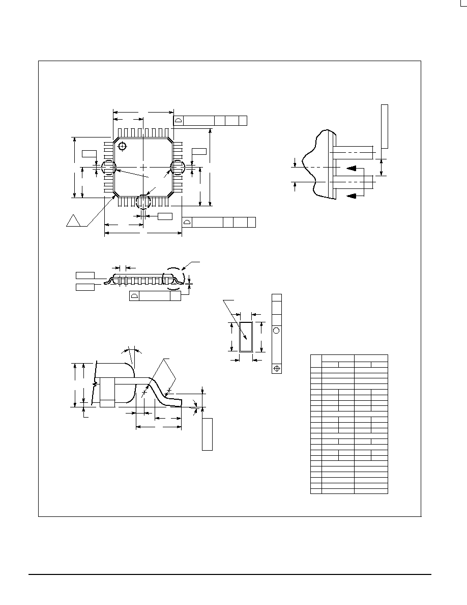
OUTLINE DIMENSIONS
FA SUFFIX
PLASTIC TQFP PACKAGE
CASE 873A≠02
ISSUE A
……
……
……
……
DETAIL Y
A
S1
V
B
1
8
9
17
25
32
AE
AE
P
DETAIL Y
BASE
N
J
D
F
METAL
SECTION AE≠AE
G
SEATING
PLANE
R
Q
_
W
K
X
0.250 (0.010)
GAUGE PLANE
E
C
H
DETAIL AD
NOTES:
1. DIMENSIONING AND TOLERANCING PER ANSI
Y14.5M, 1982.
2. CONTROLLING DIMENSION: MILLIMETER.
3. DATUM PLANE ≠AB≠ IS LOCATED AT BOTTOM OF
LEAD AND IS COINCIDENT WITH THE LEAD
WHERE THE LEAD EXITS THE PLASTIC BODY AT
THE BOTTOM OF THE PARTING LINE.
4. DATUMS ≠T≠, ≠U≠, AND ≠Z≠ TO BE DETERMINED
AT DATUM PLANE ≠AB≠.
5. DIMENSIONS S AND V TO BE DETERMINED AT
SEATING PLANE ≠AC≠.
6. DIMENSIONS A AND B DO NOT INCLUDE MOLD
PROTRUSION. ALLOWABLE PROTRUSION IS
0.250 (0.010) PER SIDE. DIMENSIONS A AND B
DO INCLUDE MOLD MISMATCH AND ARE
DETERMINED AT DATUM PLANE ≠AB≠.
7. DIMENSION D DOES NOT INCLUDE DAMBAR
PROTRUSION. DAMBAR PROTRUSION SHALL
NOT CAUSE THE D DIMENSION TO EXCEED
0.520 (0.020).
8. MINIMUM SOLDER PLATE THICKNESS SHALL BE
0.0076 (0.0003).
9. EXACT SHAPE OF EACH CORNER MAY VARY
FROM DEPICTION.
DIM
A
MIN
MAX
MIN
MAX
INCHES
7.000 BSC
0.276 BSC
MILLIMETERS
B
7.000 BSC
0.276 BSC
C
1.400
1.600
0.055
0.063
D
0.300
0.450
0.012
0.018
E
1.350
1.450
0.053
0.057
F
0.300
0.400
0.012
0.016
G
0.800 BSC
0.031 BSC
H
0.050
0.150
0.002
0.006
J
0.090
0.200
0.004
0.008
K
0.500
0.700
0.020
0.028
M
12 REF
12 REF
N
0.090
0.160
0.004
0.006
P
0.400 BSC
0.016 BSC
Q
1
5
1
5
R
0.150
0.250
0.006
0.010
V
9.000 BSC
0.354 BSC
V1
4.500 BSC
0.177 BSC
_
_
_
_
_
_
DETAIL AD
A1
B1
V1
4X
S
4X
B1
3.500 BSC
0.138 BSC
A1
3.500 BSC
0.138 BSC
S
9.000 BSC
0.354 BSC
S1
4.500 BSC
0.177 BSC
W
0.200 REF
0.008 REF
X
1.000 REF
0.039 REF
9
≠T≠
≠Z≠
≠U≠
T≠U
0.20 (0.008)
Z
AC
T≠U
0.20 (0.008)
Z
AB
0.10 (0.004) AC
≠AC≠
≠AB≠
M
_
8X
≠T≠, ≠U≠, ≠Z≠
T≠U
M
0.20 (0.008)
Z
AC
MC100EP111
TIMING SOLUTIONS
BR1333 -- Rev 6
5
MOTOROLA
Motorola reserves the right to make changes without further notice to any products herein. Motorola makes no warranty, representation or guarantee regarding
the suitability of its products for any particular purpose, nor does Motorola assume any liability arising out of the application or use of any product or circuit, and
specifically disclaims any and all liability, including without limitation consequential or incidental damages. "Typical" parameters which may be provided in Motorola
data sheets and/or specifications can and do vary in different applications and actual performance may vary over time. All operating parameters, including "Typicals"
must be validated for each customer application by customer's technical experts. Motorola does not convey any license under its patent rights nor the rights of
others. Motorola products are not designed, intended, or authorized for use as components in systems intended for surgical implant into the body, or other
applications intended to support or sustain life, or for any other application in which the failure of the Motorola product could create a situation where personal injury
or death may occur. Should Buyer purchase or use Motorola products for any such unintended or unauthorized application, Buyer shall indemnify and hold Motorola
and its officers, employees, subsidiaries, affiliates, and distributors harmless against all claims, costs, damages, and expenses, and reasonable attorney fees
arising out of, directly or indirectly, any claim of personal injury or death associated with such unintended or unauthorized use, even if such claim alleges that
Motorola was negligent regarding the design or manufacture of the part. Motorola and are registered trademarks of Motorola, Inc. Motorola, Inc. is an Equal
Opportunity/Affirmative Action Employer.
How to reach us:
USA / EUROPE / Locations Not Listed: Motorola Literature Distribution;
JAPAN: Nippon Motorola Ltd.; Tatsumi≠SPD≠JLDC, 6F Seibu≠Butsuryu≠Center,
P.O. Box 5405; Denver, Colorado 80217. 303≠675≠2140 or 1≠800≠441≠2447
3≠14≠2 Tatsumi Koto≠Ku, Tokyo 135, Japan. 81≠3≠3521≠8315
Mfax
TM
: RMFAX0@email.sps.mot.com ≠ TOUCHTONE 602≠244≠6609
ASIA/PACIFIC: Motorola Semiconductors H.K. Ltd.; 8B Tai Ping Industrial Park,
INTERNET: http://www.mot.com/sps/
51 Ting Kok Road, Tai Po, N.T., Hong Kong. 852≠26629298
MC100EP111/D
*MC100EP111/D*