MOTOROLA
SEMICONDUCTOR TECHNICAL DATA
Order Number: MC100ES6111/D
Rev 1, 05/2002
©
Motorola, Inc. 2002
Low Voltage 2.5/3.3V
Differential ECL/PECL/HSTL
Fanout Buffer
The Motorola MC100ES6111 is a bipolar monolithic differential clock
fanout buffer. Designed for most demanding clock distribution systems,
the MC100ES6111 supports various applications that require distribution
of precisely aligned differential clock signals. Using SiGe:C technology
and a fully differential architecture, the device offers very low skew
outputs and superior digital signal characteristics. Target applications for
this clock driver is high performance clock distribution in computing,
networking and telecommunication systems.
∑
1:10 differential clock distribution
∑
35 ps maximum device skew
∑
Fully differential architecture from input to all outputs
∑
SiGe:C technology supports near-zero output skew
∑
Supports DC to 2.7 GHz operation of clock or data signals
∑
ECL/PECL compatible differential clock outputs
∑
ECL/PECL/HSTL compatible differential clock inputs
∑
Single 3.3V, -3.3V, 2.5V or -2.5V supply
∑
Standard 32 lead LQFP package
∑
Industrial temperature range
∑
Pin and function compatible to the MC100EP111
Functional Description
The MC100ES6111 is designed for low skew clock distribution systems and supports clock frequencies up to 2.7 GHz. The
device accepts two clock sources. The CLKA input can be driven by ECL or PECL compatible signals, the CLKB input accepts
HSTL compatible signals. The selected input signal is distributed to 10 identical, differential ECL/PECL outputs. If VBB is
connected to the CLKA input and bypassed to GND by a 10 nF capacitor, the MC100ES6111 can be driven by single-ended
ECL/PECL signals utilizing the VBB bias voltage output.
In order to meet the tight skew specification of the device, both outputs of a differential output pair should be terminated, even if
only one output is used. In the case where not all ten outputs are used, the output pairs on the same package side as the parts
being used on that side should be terminated.
The MC100ES6111 can be operated from a single 3.3V or 2.5V supply. As most other ECL compatible devices, the
MC100ES6111 supports positive (PECL) and negative (ECL) supplies. The MC100ES6111 is pin and function compatible to the
MC100EP111.
MC100ES6111
LOW≠VOLTAGE
1:10 DIFFERENTIAL
ECL/PECL/HSTL
CLOCK FANOUT DRIVER
FA SUFFIX
32≠LEAD LQFP PACKAGE
CASE 873A
MC100ES6111
MOTOROLA
TIMING SOLUTIONS
2
Q8
Q7
Q0
Q1
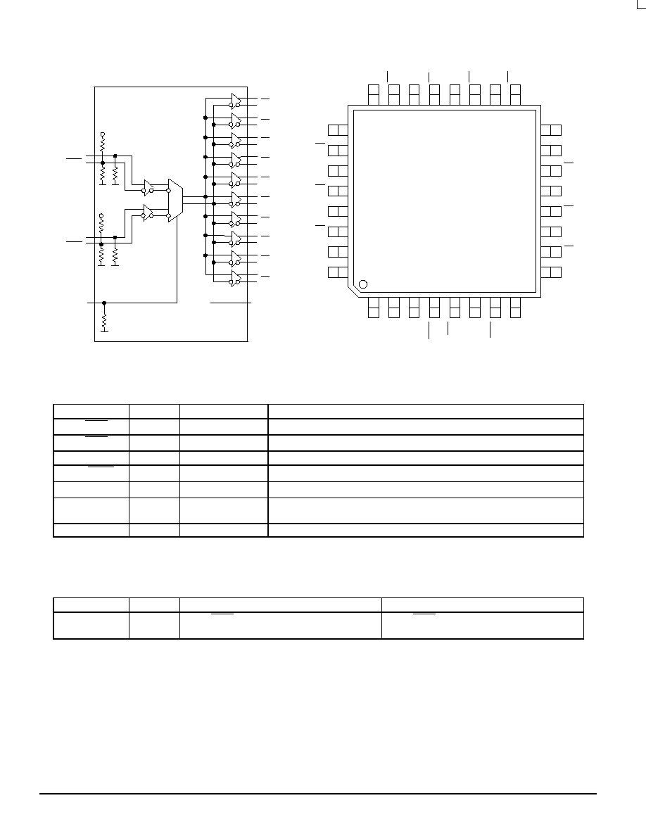
Figure 1. MC100ES6111 Logic Diagram
VCC
Q2
Q1
Q0
VCC
Q7
Q9
Q3
Q3
Q4
Q4
Q5
Q5
Q6
Q6
VCC
CLK_SEL
CLKA
CLKA
VBB
CLKB
CLKB
VEE
25
26
27
28
29
30
31
32
15
14
13
12
11
10
9
1
2
3
4
5
6
7
8
24
23
22
21
20
19
18
17
16
MC100ES6111
Figure 2. 32≠Lead Package Pinout (Top View)
VCC
VCC
Q9
Q8
Q2
0
1
CLKA
CLKA
CLKB
CLKB
CLK_SEL
VCC
VCC
Q0
Q0
Q1
Q1
Q2
Q2
Q3
Q3
Q4
Q4
Q5
Q5
Q6
Q6
Q7
Q7
Q8
Q8
Q9
Q9
VBB
Table 1. PIN CONFIGURATION
Pin
I/O
Type
Function
CLKA, CLKA
Input
ECL/PECL
Differential reference clock signal input
CLKB, CLKB
Input
HSTL
Alternative differential reference clock signal input
CLK_SEL
Input
ECL/PECL
Active clock input select
Q[0≠9], Q[0≠9]
Output
ECL/PECL
Differential clock outputs
VEEa
Supply
Negative power supply
VCC
Supply
Positive power supply. All VCC pins must be connected to the positive power
supply for correct DC and AC operation.
VBB
Output
DC
Reference voltage output for single ended ECL or PECL operation
a. In ECL mode (negative power supply mode), VEE is either ≠3.3V or ≠2.5V and VCC is connected to GND (0V). In PECL mode (positive power
supply mode), VEE is connected to GND (0V) and VCC is either +3.3V or +2.5V. In both modes, the input and output levels are referenced to
the most positive supply (VCC).
Table 2. FUNCTION TABLE
Control
Default
0
1
CLK_SEL
0
CLKA, CLKA input pair is active. CLKA can be
driven by ECL or PECL compatible signals.
CLKB, CLKB input pair is active. CLKB can be
driven by HSTL compatible signals.
MC100ES6111
TIMING SOLUTIONS
3
MOTOROLA
Table 3. Absolute Maximum Ratingsa
Symbol
Characteristics
Min
Max
Unit
Condition
VCC
Supply Voltage
-0.3
3.6
V
VIN
DC Input Voltage
-0.3
VCC + 0.3
V
VOUT
DC Output Voltage
-0.3
VCC + 0.3
V
IIN
DC Input Current
±
20
mA
IOUT
DC Output Current
±
50
mA
TS
Storage temperature
-65
125
∞
C
TFunc
Functional temperature range
TA = -40
TJ = +110
∞
C
a. Absolute maximum continuous ratings are those maximum values beyond which damage to the device may occur. Exposure to these conditions
or conditions beyond those indicated may adversely affect device reliability. Functional operation at absolute-maximum-rated conditions is not
implied.
Table 4. General Specifications
Symbol
Characteristics
Min
Typ
Max
Unit
Condition
VTT
Output termination voltage
VCC ≠ 2a
V
MM
ESD Protection (Machine model)
200
V
HBM
ESD Protection (Human body model)
4000
V
CDM
ESD Protection (Charged device model
2000
V
LU
Latch-up immunity
200
mA
CIN
4.0
pF
Inputs
JA
Thermal resistance junction to ambient
JESD 51-3, single layer test board
JESD 51-6, 2S2P multilayer test board
83.1
73.3
68.9
63.8
57.4
59.0
54.4
52.5
50.4
47.8
86.0
75.4
70.9
65.3
59.6
60.6
55.7
53.8
51.5
48.8
∞
C/W
∞
C/W
∞
C/W
∞
C/W
∞
C/W
∞
C/W
∞
C/W
∞
C/W
∞
C/W
∞
C/W
Natural convection
100 ft/min
200 ft/min
400 ft/min
800 ft/min
Natural convection
100 ft/min
200 ft/min
400 ft/min
800 ft/min
JC
Thermal resistance junction to case
23.0
26.3
∞
C/W
MIL-SPEC 883E
Method 1012.1
TJ
Operating junction temperatureb (continuous
operation)
MTBF = 9.1 years
110
∞
C
a. Output termination voltage VTT = 0V for VCC = 2.5V operation is supported but the power consumption of the device will increase
b. Operating junction temperature impacts device life time. Maximum continues operating junction temperature should be selected according
to the application life time requirements (See application note AN1545 and the application section in this datasheet for more information).
The device AC and DC parameters are specified up to 110
∞
C junction temperature allowing the MC100ES6111 to be used in applications
requiring industrial temperature range. It is recommended that users of the MC100ES6111 employ thermal modeling analysis to assist in
applying the junction temperature specifications to their particular application.
MC100ES6111
MOTOROLA
TIMING SOLUTIONS
4
Table 5. PECL/HSTL DC Characteristics (VCC = 2.5V
±
5% or VCC = 3.3V
±
5%, VEE = GND, TJ = 0
∞
C to + 110
∞
C)
Symbol
Characteristics
Min
Typ
Max
Unit
Condition
Control input CLK_SEL
VIL
Input voltage low
VCC - 1.810
VCC - 1.475
V
VIH
Input voltage high
VCC - 1.165
VCC - 0.880
V
IIN
Input Currenta
100
µ
A
VIN = VIL or VIN = VIH
Clock input pair CLKA, CLKA (PECL differential signals)
VPP
Differential input voltageb
0.1
1.3
V
Differential operation
VCMR
Differential cross point voltagec
1.0
VCC - 0.3
V
Differential operation
IIN
Input Currenta
100
µ
A
VIN = VIL or VIN = VIH
Clock input pair CLKB, CLKB (HSTL differential signals)
VDIF
Differential input voltaged
VCC = 3.3V
VCC = 2.5V
0.4
0.4
V
V
VX
Differential cross point voltagee
0.68
0.9
V
IIN
Input Current
200
µ
A
VIN = VX
±
0.2V
PECL clock outputs (Q0-9, Q0-9)
VOH
Output High Voltage
VCC-1.2
VCC-1.005
VCC-0.7
V
IOH = ≠30 mAf
VOL
Output Low Voltage
VCC = 3.3V
±
5%
VCC = 2.5V
±
5%
VCC-1.9
VCC-1.9
VCC-1.705
VCC-1.705
VCC-1.5
VCC-1.3
V
IOL = ≠5 mAf
Supply current and VBB
IEE
Maximum Quiescent Supply Current without
output termination currentg
100
mA
VEE pin
VBB
Output reference voltage
VCC - 1.4
VCC - 1.2
V
IBB = 200
µ
A
a. Input have internal pullup/pulldown resistors which affect the input current
b. VPP (DC) is the minimum differential input voltage swing required to maintain device functionality
c. VCMR (DC) is the crosspoint of the differential input signal. Functional operation is obtained when the crosspoint is within the VCMR (DC)
range and the input swing lies within the VPP (DC) specification.
d. VDIF (DC) is the minimum differential HSTL input voltage swing required for device functionality.
e. VX (DC) is the crosspoint of the differential HSTL input signal. Functional operation is obtained when the crosspoint is within the VX (DC)
range and the input swing lies within the VPP (DC) specification.
f.
Equivalent to a termination of 50
W
to VTT.
g. ICC calculation: ICC = (number of differential output pairs used) x (IOH + IOL) + IEE
ICC = (number of differential output pairs used) x (VOH ≠ VTT)/Rload + (VOL ≠ VTT)/Rload + IEE.

MC100ES6111
TIMING SOLUTIONS
5
MOTOROLA
Table 6. ECL DC Characteristics (VEE = -2.5V
±
5% or VEE = -3.3V
±
5%, VCC = GND, TJ = 0
∞
C to + 110
∞
C)
Symbol
Characteristics
Min
Typ
Max
Unit
Condition
Control input CLK_SEL
VIL
Input voltage low
-1.810
-1.475
V
VIH
Input voltage high
-1.165
-0.880
V
IIN
Input Currenta
100
µ
A
VIN = VIL or VIN = VIH
Clock input pair CLKA, CLKA, CLKB, CLKB (ECL differential signals)
VPP
Differential input voltageb
0.1
1.3
V
Differential operation
VCMR
Differential cross point voltagec
VEE + 1.0
-0.3
V
Differential operation
IIN
Input Currenta
100
µ
A
VIN = VIL or VIN = VIH
ECL clock outputs (Q0-9, Q0-9)
VOH
Output High Voltage
-1.2
-1.005
-0.7
V
IOH = ≠30 mAd
VOL
Output Low Voltage
VEE = ≠3.3V
±
5%
VEE = ≠2.5V
±
5%
-1.9
-1.9
-1.705
-1.705
-1.5
-1.3
V
IOL = ≠5 mAd
Supply current and VBB
IEE
Maximum Quiescent Supply Current
without output termination currente
100
mA
VEE pin
VBB
Output reference voltage
VCC-1.4
VCC-1.2
V
IBB = 200
µ
A
a. Input have internal pullup/pulldown resistors which affect the input current
b. VPP (DC) is the minimum differential input voltage swing required to maintain device functionality
c. VCMR (DC) is the crosspoint of the differential input signal. Functional operation is obtained when the crosspoint is within the VCMR (DC)
range and the input swing lies within the VPP (DC) specification.
d. Equivalent to a termination of 50
W
to VTT.
e. ICC calculation: ICC = (number of differential output pairs used) x (IOH + IOL) + IEE
ICC = (number of differential output pairs used) x (VOH ≠ VTT)/Rload + (VOL ≠ VTT)/Rload + IEE.