 | –≠–ª–µ–∫—Ç—Ä–æ–Ω–Ω—ã–π –∫–æ–º–ø–æ–Ω–µ–Ω—Ç: MC10116P | –°–∫–∞—á–∞—Ç—å:  PDF PDF  ZIP ZIP |

MOTOROLA
SEMICONDUCTOR TECHNICAL DATA
3≠63
REV 5
©
Motorola, Inc. 1996
3/93
Triple Line Receiver
The MC10116 is a triple differential amplifier designed for use in sensing
differential signals over long lines. The base bias supply (VBB) is made available
at pin 11 to make the device useful as a Schmitt trigger, or in other applications
where a stable reference voltage is necessary.
Active current sources provide the MC10116 with excellent common mode
noise rejection. If any amplifier in a package is not used, one input of that
amplifier must be connected to VBB (pin 11) to prevent upsetting the current
source bias network.
Complementary outputs are provided to allow driving twisted pair lines, to
enable cascading of several amplifiers in a chain, or simply to provide
complement outputs of the input logic function.
PD = 85 mW typ/pkg (No Load)
tpd = 2.0 ns typ
tr, tf = 2.0 ns typ (20%≠80%)
LOGIC DIAGRAM
VCC1 = PIN 1
VCC2 = PIN 16
VEE = PIN 8
5
4
11
3
2
10
9
7
6
13
12
15
14
VBB*
*VBB to be used to supply bias to the MC10116 only and bypassed (when used)
with 0.01
µ
F to 0.1
µ
F capacitor to ground (0 V). VBB can source < 1.0 mA.
When the input pin with the bubble goes positive, the output pin with the bubble
goes positive.
MC10116
DIP
PIN ASSIGNMENT
VCC1
AOUT
AOUT
AIN
AIN
BOUT
BOUT
VEE
VCC2
COUT
COUT
CIN
CIN
VBB
BIN
BIN
16
15
14
13
12
11
10
9
1
2
3
4
5
6
7
8
Pin assignment is for Dual≠in≠Line Package.
For PLCC pin assignment, see the Pin Conversion
Tables on page 6≠11 of the Motorola MECL Data
Book (DL122/D).
L SUFFIX
CERAMIC PACKAGE
CASE 620≠10
P SUFFIX
PLASTIC PACKAGE
CASE 648≠08
FN SUFFIX
PLCC
CASE 775≠02
MC10116
MOTOROLA
MECL Data
DL122 -- Rev 6
3≠64
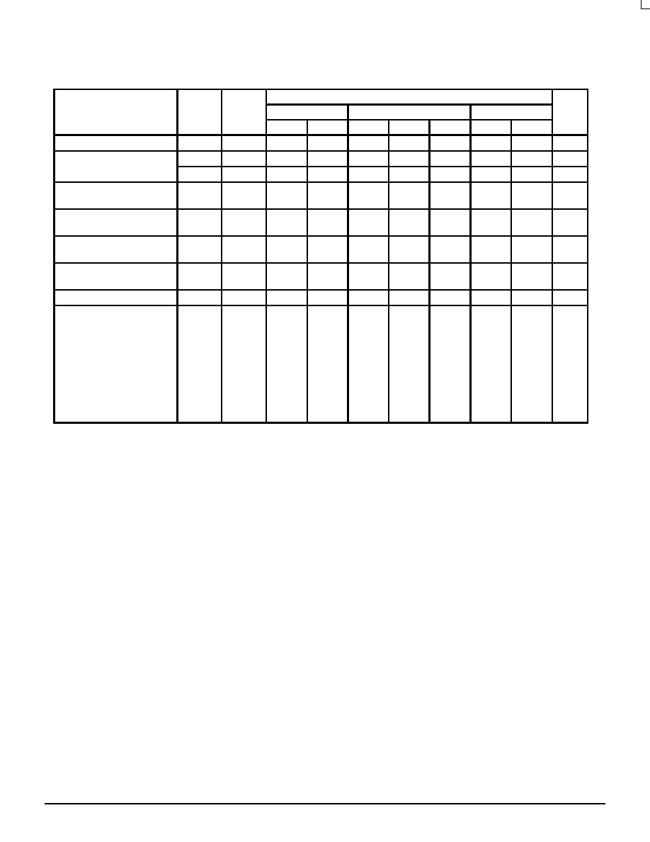
ELECTRICAL CHARACTERISTICS
Pi
Test Limits
Pin
Under
≠30
∞
C
+25
∞
C
+85
∞
C
Characteristic
Symbol
Under
Test
Min
Max
Min
Typ
Max
Min
Max
Unit
Power Supply Drain Current
IE
8
23
17
21
23
mAdc
Input Current
IinH
4
150
95
95
µ
Adc
ICBO
4
1.5
1.0
1.0
µ
Adc
Output Voltage
Logic 1
VOH
2
3
≠1.060
≠1.060
≠0.890
≠0.890
≠0.960
≠0.960
≠0.810
≠0.810
≠0.890
≠0.890
≠0.700
≠0.700
Vdc
Output Voltage
Logic 0
VOL
2
3
≠1.890
≠1.890
≠1.675
≠1.675
≠1.850
≠1.850
≠1.650
≠1.650
≠1.825
≠1.825
≠1.615
≠1.615
Vdc
Threshold Voltage
Logic 1
VOHA
2
3
≠1.080
≠1.080
≠0.980
≠0.980
≠0.910
≠0.910
Vdc
Threshold Voltage
Logic 0
VOLA
2
3
≠1.655
≠1.655
≠1.630
≠1.630
≠1.595
≠1.595
Vdc
Reference Voltage
VBB
11
≠1.420
≠1.280
≠1.350
≠1.230
≠1.295
≠1.150
Vdc
Switching Times
(50
Load)
ns
Propagation Delay
t4+2+
t4≠2≠
t4+3≠
t4≠3+
2
2
3
3
1.0
1.0
1.0
1.0
3.1
3.1
3.1
3.1
1.0
1.0
1.0
1.0
2.0
2.0
2.0
2.0
2.9
2.9
2.9
2.9
1.0
1.0
1.0
1.0
3.3
3.3
3.3
3.3
Rise Time
(20 to 80%)
t2+
t3+
2
3
1.1
1.1
3.6
3.6
1.1
1.1
2.0
2.0
3.3
3.3
1.1
1.1
3.7
3.7
Fall Time
(20 to 80%)
t2≠
t3≠
2
3
1.1
1.1
3.6
3.6
1.1
1.1
2.0
2.0
3.3
3.3
1.1
1.1
3.7
3.7
MC10116
3≠65
MOTOROLA
MECL Data
DL122 -- Rev 6
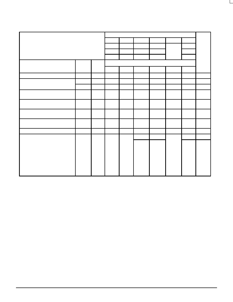
ELECTRICAL CHARACTERISTICS
(continued)
TEST VOLTAGE VALUES (Volts)
@ Test Temperature
VIHmax
VILmin
VIHAmin VILAmax
VBB
VEE
≠30
∞
C
≠0.890
≠1.890
≠1.205
≠1.500
From
≠5.2
+25
∞
C
≠0.810
≠1.850
≠1.105
≠1.475
From
Pin
11
≠5.2
+85
∞
C
≠0.700
≠1.825
≠1.035
≠1.440
11
≠5.2
Pin
Under
TEST VOLTAGE APPLIED TO PINS LISTED BELOW
(VCC)
Characteristic
Symbol
Under
Test
VIHmax
VILmin
VIHAmin VILAmax
VBB
VEE
(VCC)
Gnd
Power Supply Drain Current
IE
8
4, 9, 12
5, 10, 13
8
1, 16
Input Current
IinH
4
4
9, 12
5, 10, 13
8
1, 16
ICBO
4
9, 12
5, 10, 13
8,4
1, 16
Output Voltage
Logic 1
VOH
2
3
4
9, 12
9, 12
4
5, 10, 13
5, 10, 13
8
8
1, 16
1, 16
Output Voltage
Logic 0
VOL
2
3
9, 12
4
4
9, 12
5, 10, 13
5, 10, 13
8
8
1, 16
1, 16
Threshold Voltage
Logic 1
VOHA
2
3
9, 12
9, 12
4
4
5, 10, 13
5, 10, 13
8
8
1, 16
1, 16
Threshold Voltage
Logic 0
VOLA
2
3
9, 12
9, 12
4
4
5, 10, 13
5, 10, 13
8
8
1, 16
1, 16
Reference Voltage
VBB
11
5, 10, 13
8
1, 16
Switching Times
(50
Load)
Pulse In
Pulse Out
≠3.2 V
+2.0 V
Propagation Delay
t4+2+
t4≠2≠
t4+3≠
t4≠3+
2
2
3
3
4
4
4
4
2
2
3
3
5, 10, 13
5, 10, 13
5, 10, 13
5, 10, 13
8
8
8
8
1, 16
1, 16
1, 16
1, 16
Rise Time
(20 to 80%)
t2+
t3+
2
3
4
4
2
3
5, 10, 13
5, 10, 13
8
8
1, 16
1, 16
Fall Time
(20 to 80%)
t2≠
t3≠
2
3
4
4
2
3
5, 10, 13
5, 10, 13
8
8
1, 16
1, 16
Each MECL 10,000 series circuit has been designed to meet the dc specifications shown in the test table, after thermal equilibrium has been
established. The circuit is in a test socket or mounted on a printed circuit board and transverse air flow greater than 500 linear fpm is maintained.
Outputs are terminated through a 50-ohm resistor to ≠2.0 volts. Test procedures are shown for only one gate. The other gates are tested in the
same manner.
MC10116
MOTOROLA
MECL Data
DL122 -- Rev 6
3≠66
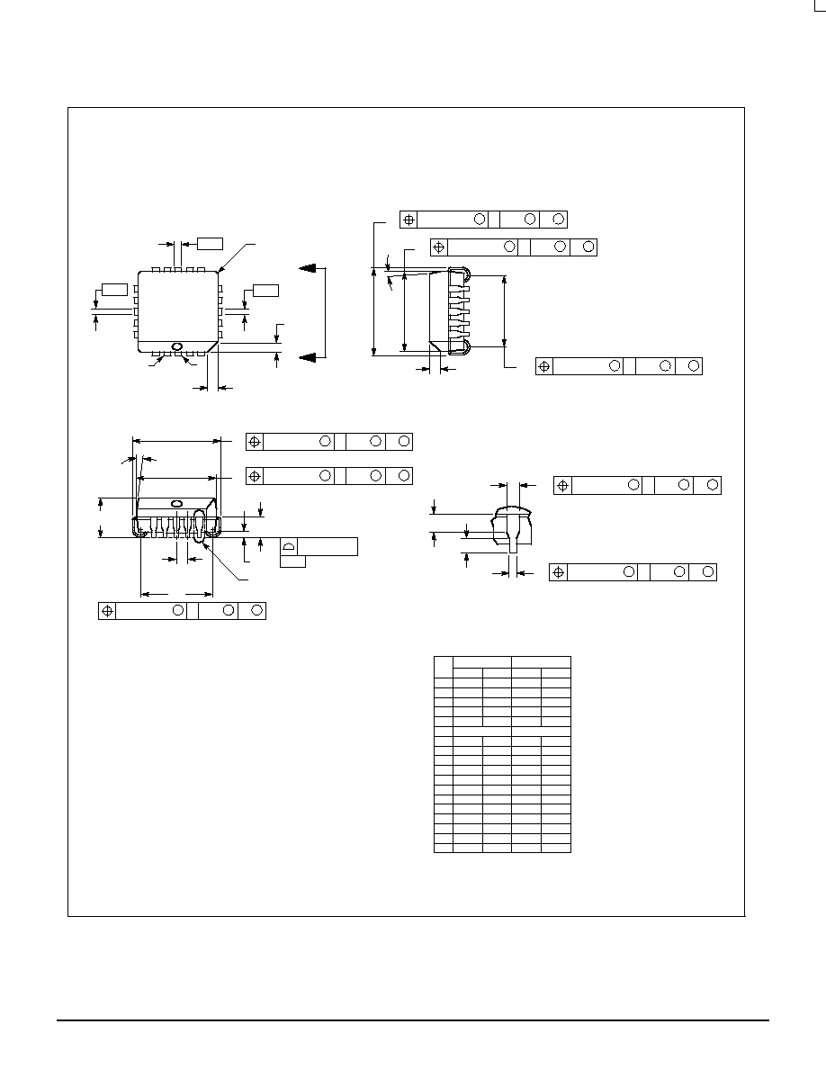
OUTLINE DIMENSIONS
FN SUFFIX
PLASTIC PLCC PACKAGE
CASE 775≠02
ISSUE C
NOTES:
1. DATUMS ≠L≠, ≠M≠, AND ≠N≠ DETERMINED
WHERE TOP OF LEAD SHOULDER EXITS PLASTIC
BODY AT MOLD PARTING LINE.
2. DIMENSION G1, TRUE POSITION TO BE
MEASURED AT DATUM ≠T≠, SEATING PLANE.
3. DIMENSIONS R AND U DO NOT INCLUDE MOLD
FLASH. ALLOWABLE MOLD FLASH IS 0.010 (0.250)
PER SIDE.
4. DIMENSIONING AND TOLERANCING PER ANSI
Y14.5M, 1982.
5. CONTROLLING DIMENSION: INCH.
6. THE PACKAGE TOP MAY BE SMALLER THAN THE
PACKAGE BOTTOM BY UP TO 0.012 (0.300).
DIMENSIONS R AND U ARE DETERMINED AT THE
OUTERMOST EXTREMES OF THE PLASTIC BODY
EXCLUSIVE OF MOLD FLASH, TIE BAR BURRS,
GATE BURRS AND INTERLEAD FLASH, BUT
INCLUDING ANY MISMATCH BETWEEN THE TOP
AND BOTTOM OF THE PLASTIC BODY.
7. DIMENSION H DOES NOT INCLUDE DAMBAR
PROTRUSION OR INTRUSION. THE DAMBAR
PROTRUSION(S) SHALL NOT CAUSE THE H
DIMENSION TO BE GREATER THAN 0.037 (0.940).
THE DAMBAR INTRUSION(S) SHALL NOT CAUSE
THE H DIMENSION TO BE SMALLER THAN 0.025
(0.635).
≠M≠
≠N≠
≠L≠
Y BRK
W
V
D
D
S
L≠M
M
0.007 (0.180)
N
S
T
S
L≠M
M
0.007 (0.180)
N
S
T
S
L≠M
S
0.010 (0.250)
N
S
T
X
G1
B
U
Z
VIEW D≠D
20
1
S
L≠M
M
0.007 (0.180)
N
S
T
S
L≠M
M
0.007 (0.180)
N
S
T
S
L≠M
S
0.010 (0.250)
N
S
T
C
G
VIEW S
E
J
R
Z
A
0.004 (0.100)
≠T≠
SEATING
PLANE
S
L≠M
M
0.007 (0.180)
N
S
T
S
L≠M
M
0.007 (0.180)
N
S
T
H
VIEW S
K
K1
F
G1
DIM
MIN
MAX
MIN
MAX
MILLIMETERS
INCHES
A
0.385
0.395
9.78
10.03
B
0.385
0.395
9.78
10.03
C
0.165
0.180
4.20
4.57
E
0.090
0.110
2.29
2.79
F
0.013
0.019
0.33
0.48
G
0.050 BSC
1.27 BSC
H
0.026
0.032
0.66
0.81
J
0.020
≠≠≠
0.51
≠≠≠
K
0.025
≠≠≠
0.64
≠≠≠
R
0.350
0.356
8.89
9.04
U
0.350
0.356
8.89
9.04
V
0.042
0.048
1.07
1.21
W
0.042
0.048
1.07
1.21
X
0.042
0.056
1.07
1.42
Y
≠≠≠
0.020
≠≠≠
0.50
Z
2
10
2
10
G1
0.310
0.330
7.88
8.38
K1
0.040
≠≠≠
1.02
≠≠≠
_
_
_
_
MC10116
3≠67
MOTOROLA
MECL Data
DL122 -- Rev 6
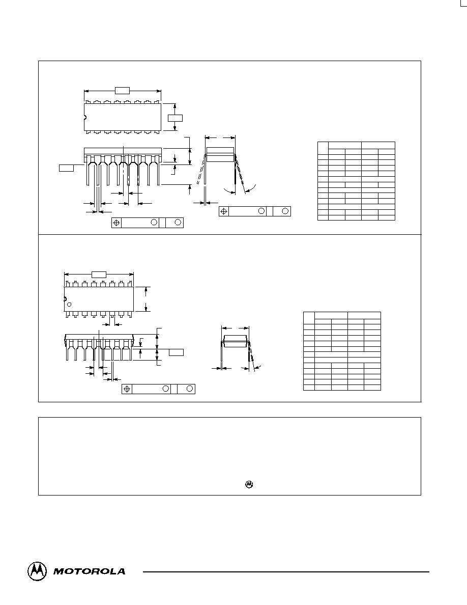
OUTLINE DIMENSIONS
P SUFFIX
PLASTIC DIP PACKAGE
CASE 648≠08
ISSUE R
NOTES:
1. DIMENSIONING AND TOLERANCING PER ANSI
Y14.5M, 1982.
2. CONTROLLING DIMENSION: INCH.
3. DIMENSION L TO CENTER OF LEADS WHEN
FORMED PARALLEL.
4. DIMENSION B DOES NOT INCLUDE MOLD FLASH.
5. ROUNDED CORNERS OPTIONAL.
≠A≠
B
F
C
S
H
G
D
J
L
M
16 PL
SEATING
1
8
9
16
K
PLANE
≠T≠
M
A
M
0.25 (0.010)
T
DIM
MIN
MAX
MIN
MAX
MILLIMETERS
INCHES
A
0.740
0.770
18.80
19.55
B
0.250
0.270
6.35
6.85
C
0.145
0.175
3.69
4.44
D
0.015
0.021
0.39
0.53
F
0.040
0.70
1.02
1.77
G
0.100 BSC
2.54 BSC
H
0.050 BSC
1.27 BSC
J
0.008
0.015
0.21
0.38
K
0.110
0.130
2.80
3.30
L
0.295
0.305
7.50
7.74
M
0
10
0
10
S
0.020
0.040
0.51
1.01
_
_
_
_
L SUFFIX
CERAMIC DIP PACKAGE
CASE 620≠10
ISSUE V
NOTES:
1. DIMENSIONING AND TOLERANCING PER
ANSI Y14.5M, 1982.
2. CONTROLLING DIMENSION: INCH.
3. DIMENSION L TO CENTER OF LEAD WHEN
FORMED PARALLEL.
4. DIMENSION F MAY NARROW TO 0.76 (0.030)
WHERE THE LEAD ENTERS THE CERAMIC
BODY.
≠A≠
≠B≠
≠T≠
F
E
G
N
K
C
SEATING
PLANE
16 PL
D
S
A
M
0.25 (0.010)
T
16 PL
J
S
B
M
0.25 (0.010)
T
M
L
DIM
MIN
MAX
MIN
MAX
MILLIMETERS
INCHES
A
0.750
0.785
19.05
19.93
B
0.240
0.295
6.10
7.49
C
≠≠≠
0.200
≠≠≠
5.08
D
0.015
0.020
0.39
0.50
E
0.050 BSC
1.27 BSC
F
0.055
0.065
1.40
1.65
G
0.100 BSC
2.54 BSC
H
0.008
0.015
0.21
0.38
K
0.125
0.170
3.18
4.31
L
0.300 BSC
7.62 BSC
M
0
15
0
15
N
0.020
0.040
0.51
1.01
_
_
_
_
16
9
1
8
Motorola reserves the right to make changes without further notice to any products herein. Motorola makes no warranty, representation or guarantee regarding
the suitability of its products for any particular purpose, nor does Motorola assume any liability arising out of the application or use of any product or circuit, and
specifically disclaims any and all liability, including without limitation consequential or incidental damages. "Typical" parameters which may be provided in Motorola
data sheets and/or specifications can and do vary in different applications and actual performance may vary over time. All operating parameters, including "Typicals"
must be validated for each customer application by customer's technical experts. Motorola does not convey any license under its patent rights nor the rights of
others. Motorola products are not designed, intended, or authorized for use as components in systems intended for surgical implant into the body, or other
applications intended to support or sustain life, or for any other application in which the failure of the Motorola product could create a situation where personal injury
or death may occur. Should Buyer purchase or use Motorola products for any such unintended or unauthorized application, Buyer shall indemnify and hold Motorola
and its officers, employees, subsidiaries, affiliates, and distributors harmless against all claims, costs, damages, and expenses, and reasonable attorney fees
arising out of, directly or indirectly, any claim of personal injury or death associated with such unintended or unauthorized use, even if such claim alleges that
Motorola was negligent regarding the design or manufacture of the part. Motorola and are registered trademarks of Motorola, Inc. Motorola, Inc. is an Equal
Opportunity/Affirmative Action Employer.
How to reach us:
USA/EUROPE/Locations Not Listed: Motorola Literature Distribution;
JAPAN: Nippon Motorola Ltd.; Tatsumi≠SPD≠JLDC, 6F Seibu≠Butsuryu≠Center,
P.O. Box 20912; Phoenix, Arizona 85036. 1≠800≠441≠2447 or 602≠303≠5454
3≠14≠2 Tatsumi Koto≠Ku, Tokyo 135, Japan. 03≠81≠3521≠8315
MFAX: RMFAX0@email.sps.mot.com ≠ TOUCHTONE 602≠244≠6609
ASIA/PACIFIC: Motorola Semiconductors H.K. Ltd.; 8B Tai Ping Industrial Park,
INTERNET: http://Design≠NET.com
51 Ting Kok Road, Tai Po, N.T., Hong Kong. 852≠26629298
MC10116/D
*MC10116/D*