 | –≠–ª–µ–∫—Ç—Ä–æ–Ω–Ω—ã–π –∫–æ–º–ø–æ–Ω–µ–Ω—Ç: MC14528BD | –°–∫–∞—á–∞—Ç—å:  PDF PDF  ZIP ZIP |

MOTOROLA CMOS LOGIC DATA
1
MC14528B
Dual Monostable Multivibrator
The MC14528B is a dual, retriggerable, resettable monostable multivibra-
tor. It may be triggered from either edge of an input pulse, and produces an
output pulse over a wide range of widths, the duration of which is determined
by the external timing components, CX and RX.
∑
Separate Reset Available
∑
Diode Protection on All Inputs
∑
Triggerable from Leading or Trailing Edge Pulse
∑
Supply Voltage Range = 3.0 Vdc to 18 Vdc
∑
Capable of Driving Two Low≠power TTL Loads or One Low≠power
Schottky TTL Load Over the Rated Temperature Range
∑
Pin≠for≠Pin Replacement with the MC14538B
ŒŒŒŒŒŒŒŒŒŒŒŒŒŒŒŒŒŒŒŒŒ
ŒŒŒŒŒŒŒŒŒŒŒŒŒŒŒŒŒŒŒŒŒ
ŒŒŒŒŒŒŒŒŒŒŒŒŒŒŒŒŒŒŒŒŒ
ŒŒŒŒŒŒŒŒŒŒŒŒŒŒŒŒŒŒŒŒŒ
MAXIMUM RATINGS*
(Voltages Referenced to VSS)
ŒŒŒŒ
ŒŒŒŒ
ŒŒŒŒ
ŒŒŒŒ
Symbol
ŒŒŒŒŒŒŒŒŒŒŒ
ŒŒŒŒŒŒŒŒŒŒŒ
ŒŒŒŒŒŒŒŒŒŒŒ
ŒŒŒŒŒŒŒŒŒŒŒ
Parameter
ŒŒŒŒŒŒ
ŒŒŒŒŒŒ
ŒŒŒŒŒŒ
ŒŒŒŒŒŒ
Value
ŒŒŒ
ŒŒŒ
ŒŒŒ
ŒŒŒ
Unit
ŒŒŒŒ
ŒŒŒŒ
ŒŒŒŒ
ŒŒŒŒ
VDD
ŒŒŒŒŒŒŒŒŒŒŒ
ŒŒŒŒŒŒŒŒŒŒŒ
ŒŒŒŒŒŒŒŒŒŒŒ
ŒŒŒŒŒŒŒŒŒŒŒ
DC Supply Voltage
ŒŒŒŒŒŒ
ŒŒŒŒŒŒ
ŒŒŒŒŒŒ
ŒŒŒŒŒŒ
≠ 0.5 to + 18.0
ŒŒŒ
ŒŒŒ
ŒŒŒ
ŒŒŒ
V
ŒŒŒŒ
ŒŒŒŒ
ŒŒŒŒ
ŒŒŒŒ
Vin, Vout
ŒŒŒŒŒŒŒŒŒŒŒ
ŒŒŒŒŒŒŒŒŒŒŒ
ŒŒŒŒŒŒŒŒŒŒŒ
ŒŒŒŒŒŒŒŒŒŒŒ
Input or Output Voltage (DC or Transient)
ŒŒŒŒŒŒ
ŒŒŒŒŒŒ
ŒŒŒŒŒŒ
ŒŒŒŒŒŒ
≠ 0.5 to VDD + 0.5
ŒŒŒ
ŒŒŒ
ŒŒŒ
ŒŒŒ
V
ŒŒŒŒ
ŒŒŒŒ
ŒŒŒŒ
ŒŒŒŒ
Iin, Iout
ŒŒŒŒŒŒŒŒŒŒŒ
ŒŒŒŒŒŒŒŒŒŒŒ
ŒŒŒŒŒŒŒŒŒŒŒ
ŒŒŒŒŒŒŒŒŒŒŒ
Input or Output Current (DC or Transient),
per Pin
ŒŒŒŒŒŒ
ŒŒŒŒŒŒ
ŒŒŒŒŒŒ
ŒŒŒŒŒŒ
±
10
ŒŒŒ
ŒŒŒ
ŒŒŒ
ŒŒŒ
mA
ŒŒŒŒ
ŒŒŒŒ
ŒŒŒŒ
ŒŒŒŒ
PD
ŒŒŒŒŒŒŒŒŒŒŒ
ŒŒŒŒŒŒŒŒŒŒŒ
ŒŒŒŒŒŒŒŒŒŒŒ
ŒŒŒŒŒŒŒŒŒŒŒ
Power Dissipation, per Package
ŒŒŒŒŒŒ
ŒŒŒŒŒŒ
ŒŒŒŒŒŒ
ŒŒŒŒŒŒ
500
ŒŒŒ
ŒŒŒ
ŒŒŒ
ŒŒŒ
mW
ŒŒŒŒ
ŒŒŒŒ
ŒŒŒŒ
ŒŒŒŒ
Tstg
ŒŒŒŒŒŒŒŒŒŒŒ
ŒŒŒŒŒŒŒŒŒŒŒ
ŒŒŒŒŒŒŒŒŒŒŒ
ŒŒŒŒŒŒŒŒŒŒŒ
Storage Temperature
ŒŒŒŒŒŒ
ŒŒŒŒŒŒ
ŒŒŒŒŒŒ
ŒŒŒŒŒŒ
≠ 65 to + 150
ŒŒŒ
ŒŒŒ
ŒŒŒ
ŒŒŒ
_
C
ŒŒŒŒ
ŒŒŒŒ
ŒŒŒŒ
ŒŒŒŒ
TL
ŒŒŒŒŒŒŒŒŒŒŒ
ŒŒŒŒŒŒŒŒŒŒŒ
ŒŒŒŒŒŒŒŒŒŒŒ
ŒŒŒŒŒŒŒŒŒŒŒ
Lead Temperature (8≠Second Soldering)
ŒŒŒŒŒŒ
ŒŒŒŒŒŒ
ŒŒŒŒŒŒ
ŒŒŒŒŒŒ
260
ŒŒŒ
ŒŒŒ
ŒŒŒ
ŒŒŒ
_
C
* Maximum Ratings are those values beyond which damage to the device may occur.
Temperature Derating:
Plastic "P and D/DW" Packages: ≠ 7.0 mW/
_
C From 65
_
C To 125
_
C
Ceramic "L" Packages: ≠ 12 mW/
_
C From 100
_
C To 125
_
C
ONE≠SHOT SELECTION GUIDE
100 ns
1
m
s
10
m
s
100
m
s
1 ms
10 ms
100 ms
1 s
10 s
MC14528B
MC14536B
MC14538B
MC14541B
MC4538A*
23 HR
5 MIN.
TOTAL OUTPUT PULSE WIDTH RANGE
RECOMMENDED PULSE WIDTH RANGE
*LIMITED OPERATING VOLTAGE (2≠6 V)
MOTOROLA
SEMICONDUCTOR TECHNICAL DATA
©
Motorola, Inc. 1995
REV 3
1/94
MC14528B
L SUFFIX
CERAMIC
CASE 620
ORDERING INFORMATION
MC14XXXBCP
Plastic
MC14XXXBCL
Ceramic
MC14XXXBD
SOIC
TA = ≠ 55
∞
to 125
∞
C for all packages.
P SUFFIX
PLASTIC
CASE 648
D SUFFIX
SOIC
CASE 751B
BLOCK DIAGRAM
RESET 1
RESET 2
VDD
VDD
Q1
Q1
Q2
Q2
A1
B1
A2
B2
CX1
CX2
RX2
RX1
1
2
4
5
3
6
7
14
15
12
11
13
10
9
VDD = PIN 16
VSS = PIN 1, PIN 8, PIN 15
RX AND CX ARE EXTERNAL COMPONENTS
MOTOROLA CMOS LOGIC DATA
MC14528B
2
ŒŒŒŒŒŒŒŒŒŒŒŒŒŒŒŒŒŒŒŒŒŒŒŒŒŒŒŒŒŒŒŒŒŒ
ŒŒŒŒŒŒŒŒŒŒŒŒŒŒŒŒŒŒŒŒŒŒŒŒŒŒŒŒŒŒŒŒŒŒ
ŒŒŒŒŒŒŒŒŒŒŒŒŒŒŒŒŒŒŒŒŒŒŒŒŒŒŒŒŒŒŒŒŒŒ
ŒŒŒŒŒŒŒŒŒŒŒŒŒŒŒŒŒŒŒŒŒŒŒŒŒŒŒŒŒŒŒŒŒŒ
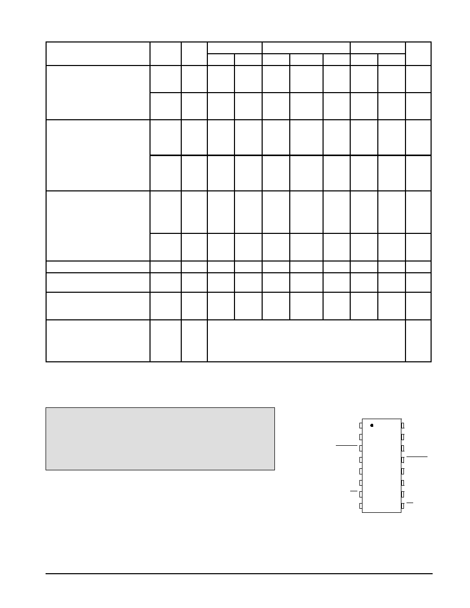
ELECTRICAL CHARACTERISTICS
(Voltages Referenced to VSS)
Characteristic
Symbol
VDD
Vdc
≠ 55
_
C
25
_
C
125
_
C
Unit
Characteristic
Symbol
DD
Vdc
Min
Max
Min
Typ #
Max
Min
Max
Unit
Output Voltage
"0" Level
Vin = VDD or 0
"1" Level
Vin = 0 or VDD
VOL
5.0
10
15
--
--
--
0.05
0.05
0.05
--
--
--
0
0
0
0.05
0.05
0.05
--
--
--
0.05
0.05
0.05
Vdc
"1" Level
Vin = 0 or VDD
VOH
5.0
10
15
4.95
9.95
14.95
--
--
--
4.95
9.95
14.95
5.0
10
15
--
--
--
4.95
9.95
14.95
--
--
--
Vdc
Input Voltage
"0" Level
(VO = 4.5 or 0.5 Vdc)
(VO = 9.0 or 1.0 Vdc)
(VO = 13.5 or 1.5 Vdc)
"1" Level
(VO = 0.5 or 4.5 Vdc)
(VO = 1.0 or 9.0 Vdc)
(VO = 1.5 or 13.5 Vdc)
VIL
5.0
10
15
--
--
--
1.5
3.0
4.0
--
--
--
2.25
4.50
6.75
1.5
3.0
4.0
--
--
--
1.5
3.0
4.0
Vdc
"1" Level
(VO = 0.5 or 4.5 Vdc)
(VO = 1.0 or 9.0 Vdc)
(VO = 1.5 or 13.5 Vdc)
VIH
5.0
10
15
3.5
7.0
11
--
--
--
3.5
7.0
11
2.75
5.50
8.25
--
--
--
3.5
7.0
11
--
--
--
Vdc
Output Drive Current
(VOH = 2.5 Vdc)
Source
(VOH = 4.6 Vdc)
(VOH = 9.5 Vdc)
(VOH = 13.5 Vdc)
IOH
5.0
5.0
10
15
≠ 1.2
≠ 0.64
≠ 1.6
≠ 4.2
--
--
--
--
≠ 1.0
≠ 0.51
≠ 1.3
≠ 3.4
≠ 1.7
≠ 0.88
≠ 2.25
≠ 8.8
--
--
--
--
≠ 0.7
≠ 0.36
≠ 0.9
≠ 2.4
--
--
--
--
mAdc
(VOL = 0.4 Vdc)
Sink
(VOL = 0.5 Vdc)
(VOL = 1.5 Vdc)
IOL
5.0
10
15
0.64
1.6
4.2
--
--
--
0.51
1.3
3.4
0.88
2.25
8.8
--
--
--
0.36
0.9
2.4
--
--
--
mAdc
Input Current
Iin
15
--
±
0.1
--
±
0.00001
±
0.1
--
±
1.0
µ
Adc
Input Capacitance
(Vin = 0)
Cin
--
--
--
--
5.0
7.5
--
--
pF
Quiescent Current
(Per Package)
IDD
5.0
10
15
--
--
--
5.0
10
20
--
--
--
0.005
0.010
0.015
5.0
10
20
--
--
--
150
300
600
µ
Adc
**Total Supply Current at an
external load Capacitance (CL)
and at external timing
capacitance (CX), use the
formula --
IT
--
IT(CL, CX) = [(CL + 0.36CX)VDDf + 2x10≠8
RXCX(VDD≠2)2f] x 10≠3
where: IT in
µ
A (per circuit), CL and CX in pF, RX in megohms,
VDD in Vdc, f in kHz is input frequency.
µ
Adc
#Data labelled "Typ" is not to be used for design purposes but is intended as an indication of the IC's potential performance.
** The formulas given are for the typical characteristics only at 25
_
C.
This device contains protection circuitry to guard against damage
due to high static voltages or electric fields. However, precautions must
be taken to avoid applications of any voltage higher than maximum rated
voltages to this high-impedance circuit. For proper operation, Vin and
Vout should be constrained to the range VSS
(Vin or Vout)
VDD.
Unused inputs must always be tied to an appropriate logic voltage
level (e.g., either VSS or VDD). Unused outputs must be left open.
PIN ASSIGNMENT
13
14
15
16
9
10
11
12
5
4
3
2
1
8
7
6
A2
RESET 2
CX2/RX2
VSS
VDD
Q2
Q2
B2
A1
RESET 1
CX1/RX1
VSS
VSS
Q1
Q1
B1
MOTOROLA CMOS LOGIC DATA
3
MC14528B
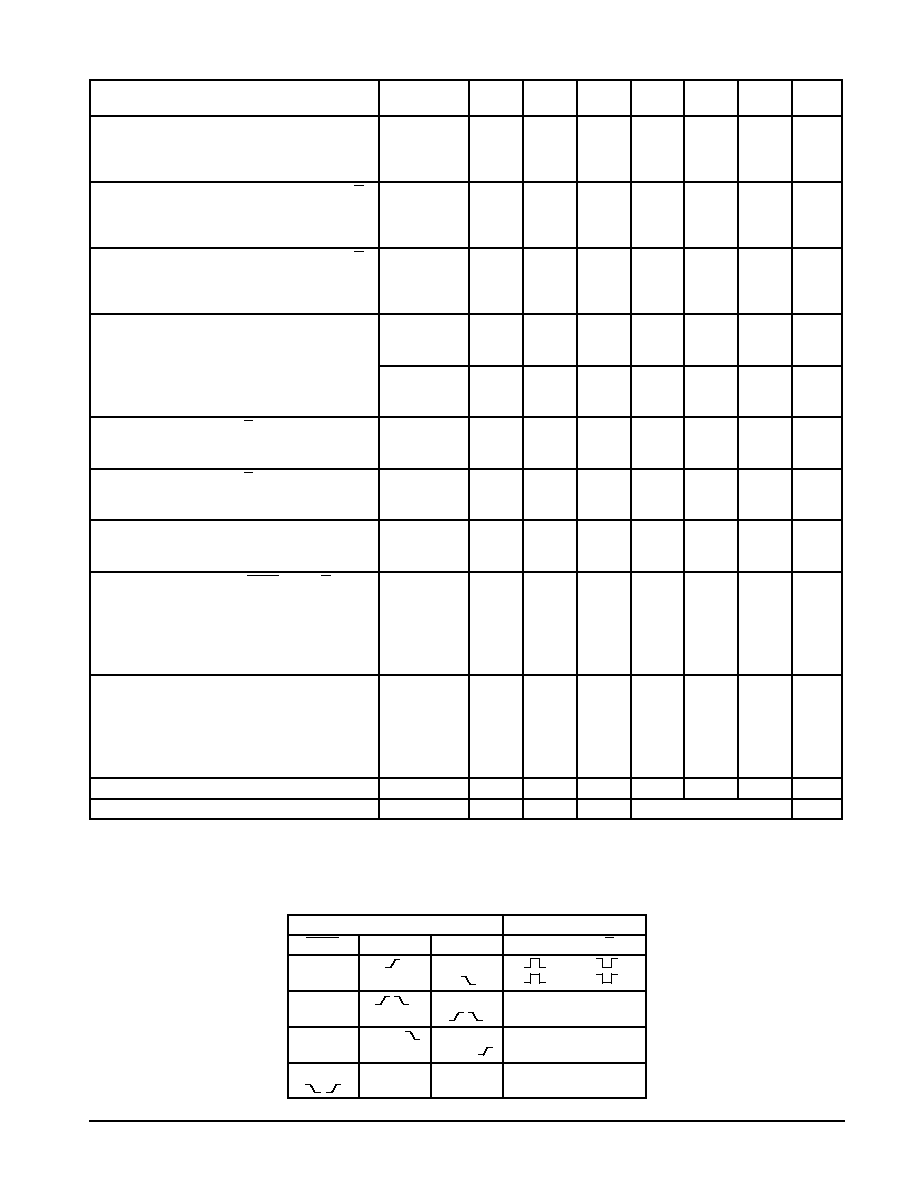
SWITCHING CHARACTERISTICS**
(CL = 50 pF, TA = 25
_
C)
Characteristic
Symbol
CX
pF
RX
k
VDD
Vdc
Min
Typ #
Max
Unit
Output Rise and Fall Time
tTLH, tTHL = (1.5 ns/pF) CL + 25 ns
tTLH, tTHL = (0.75 ns/pF) CL + 12.5 ns
tTLH, tTHL = (0.55 ns/pF) CL + 9.5 ns
tTLH,
tTHL
--
--
5.0
10
15
--
--
--
100
50
40
200
100
80
ns
Turn≠Off, Turn≠On Delay Time -- A or B to Q or Q
tPLH, tPHL = (1.7 ns/pF) CL + 240 ns
tPLH, tPHL = (0.66 ns/pF) CL + 87 ns
tPLH, tPHL = (0.5 ns/pF) CL + 65 ns
tPLH,
tPHL
15
5.0
5.0
10
15
--
--
--
325
120
90
650
240
180
ns
Turn≠Off, Turn≠On Delay Time -- A or B to Q or Q
tPLH, tPHL = (1.7 ns/pF) CL + 620 ns
tPLH, tPHL = (0.66 ns/pF) CL + 257 ns
tPLH, tPHL = (0.5 ns/pF) CL + 185 ns
tPLH,
tPHL
1000
10
5.0
10
15
--
--
--
705
290
210
--
--
--
ns
Input Pulse Width -- A or B
tWH
15
5.0
5.0
10
15
150
75
55
70
30
30
--
--
--
ns
tWL
1000
10
5.0
10
15
--
--
--
70
30
30
--
--
--
ns
Output Pulse Width -- Q or Q
(For CX < 0.01
µ
F use graph for
appropriate VDD level.)
tW
15
5.0
5.0
10
15
--
--
--
550
350
300
--
--
--
ns
Output Pulse Width -- Q or Q
(For CX > 0.01
µ
F use formula:
tW = 0.2 RX CX Ln [VDD ≠ VSS])
tW
10,000
10
5.0
10
15
15
10
15
30
50
55
45
90
95
µ
s
Pulse Width Match between Circuits in the same
package
t1 ≠ t2
10,000
10
5.0
10
15
--
--
--
6.0
8.0
8.0
25
35
35
%
Reset Propagation Delay -- Reset to Q or Q
tPLH,
tPHL
15
5.0
5.0
10
15
--
--
--
325
90
60
600
225
170
ns
1000
10
5.0
10
15
--
--
--
1000
300
250
--
--
--
ns
Retrigger Time
trr
15
5.0
5.0
10
15
0
0
0
--
--
--
--
--
--
ns
1000
10
5.0
10
15
0
0
0
--
--
--
--
--
--
ns
External Timing Resistance
RX
--
--
--
5.0
--
1000
k
External Timing Capacitance
CX
--
--
--
No Limits*
µ
F
RX is in Ohms, CX is in farads, VDD and VSS in volts, PWout in seconds.
* If CX > 15
µ
F, Use Discharge Protection Diode DX, per Fig. 9.
** The formulas given are for the typical characteristics only at 25
_
C.
#Data labelled "Typ" is not to be used for design purposes but is intended as an indication of the IC's potential performance.
FUNCTION TABLE
Inputs
Outputs
Reset
A
B
Q
Q
H
H
H
L
H
L
Not Triggered
H
H
Not Triggered
H
L, H,
H
Not Triggered
H
L
L, H,
Not Triggered
L
X
X
L
H
X
X
Not Triggered
MOTOROLA CMOS LOGIC DATA
MC14528B
4
Figure 1. Output Source Current Test Circuit
Figure 2. Output Sink Current Test Circuit
VDD
VDD
OPEN
VSS
VSS
OPEN
VOL
RESET
A
B
Q
Q
16
8
16
8
IOL
RESET
A
B
Q
Q
IOH
VOH
Figure 3. Power Dissipation Test Circuit and Waveforms
VDD
DUTY CYCLE = 50%
CL
CL
CL
CL
ID
500 pF
VSS
Vin
20 ns
20 ns
VDD
0 V
Vin
90%
10%
0.1
m
F
CERAMIC
RX
CX
RX
CX
A
B
RESET
A
B
RESET
Q
Q
Q
Q
ŒŒŒŒŒŒŒŒŒŒŒŒŒŒ
ŒŒŒŒŒŒŒŒŒŒŒŒŒŒ
ŒŒŒŒŒŒŒŒŒŒŒŒŒŒ
ŒŒŒŒŒŒŒŒŒŒŒŒŒŒ
INPUT CONNECTIONS
Characteristics
Reset
A
B
tPLH, tPHL, tTLH, tTHL
tW
VDD
PG1
VDD
tPLH, tPHL, tTLH, tTHL
tW
VDD
VSS
PG2
tPLH(R), tPHL(R), tW
PG3
PG1
PG2
Figure 4. AC Test Circuit
PULSE
GENERATOR
PULSE
GENERATOR
PULSE
GENERATOR
VDD
RX
CX
RX
CX
VSS
A
B
RESET
A
B
RESET
Q
Q
Q
Q
CL
CL
CL
CL
PG1 =
PG2 =
PG3 =
*CX = 15 pF
*CL = 15 pF
RX = 5.0 k
W
* Includes capacitance of probes,
wiring, and fixture parasitic.
NOTE: AC test waveforms for
PG1, PG2, and PG3 on
next page.

MOTOROLA CMOS LOGIC DATA
5
MC14528B
Figure 5. AC Test Waveforms
VDD
VSS
VDD
VSS
VDD
VSS
VOH
VOL
VOH
VOL
90%
10%
90%
10%
50%
50%
50%
50%
50%
trr
50%
tTLH
tTHL
tTLH
tTHL
90%
10%
tTLH
tTHL
tTHL
tTLH
50%
90%
10%
50%
50%
tWL
tPLH
50%
50%
50%
90%
10%
A
B
Q
Q
RESET
tWH
tTLH
tTHL
tPHL
tPHL
tPHL
tWL
tPHL
tW
Figure 6. Pulse Width versus CX
100,000
10,000
1000
100
10
CX, EXTERNAL CAPACITANCE (pF)
PULSE WIDTH ( s)
t , W
m
1000
100
10
1.0
0.1
VDD = 15 V
10 V
5.0 V
15 V
10 V
5.0 V
15 V
10 V
5.0 V
RX = 5.0 k
W
15 V
10 V
5.0 V
RX = 100 k
W
RX = 10 k
W
MOTOROLA CMOS LOGIC DATA
MC14528B
6
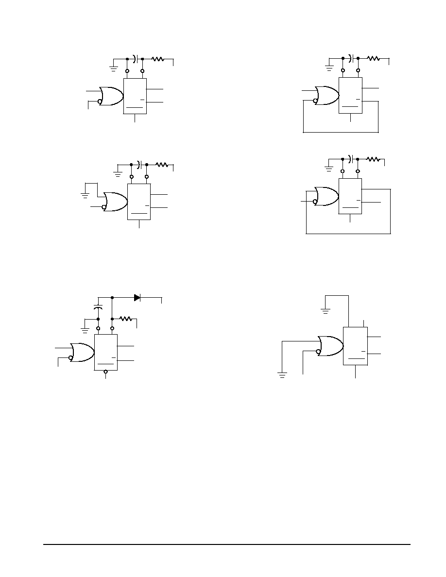
TYPICAL APPLICATIONS
Figure 7. Retriggerable
Monostables Circuitry
Figure 8. Non≠Retriggerable
Monostables Circuitry
VDD
Rx
Cx
VDD
Q
Q
RESET
FALLING EDGE
TRIGGER
RISING EDGE
TRIGGER
VDD
Rx
Cx
VDD
Q
Q
RESET
A
B
A
B
VDD
VDD
Rx
Cx
VDD
Q
Q
RESET
FALLING EDGE
TRIGGER
RISING EDGE
TRIGGER
VDD
Rx
Cx
VDD
Q
Q
RESET
A
B
A
B
Figure 9. Use of a Diode to Limit
Power Down Current Surge
Figure 10. Connection of Unused Sections
VDD
VDD
VDD
DX
Rx
Cx
VDD
Q
Q
RESET
RESET
VDD
VDD
NC
NC
NC
A
B
1, 15
2, 14
Q
Q
MOTOROLA CMOS LOGIC DATA
7
MC14528B
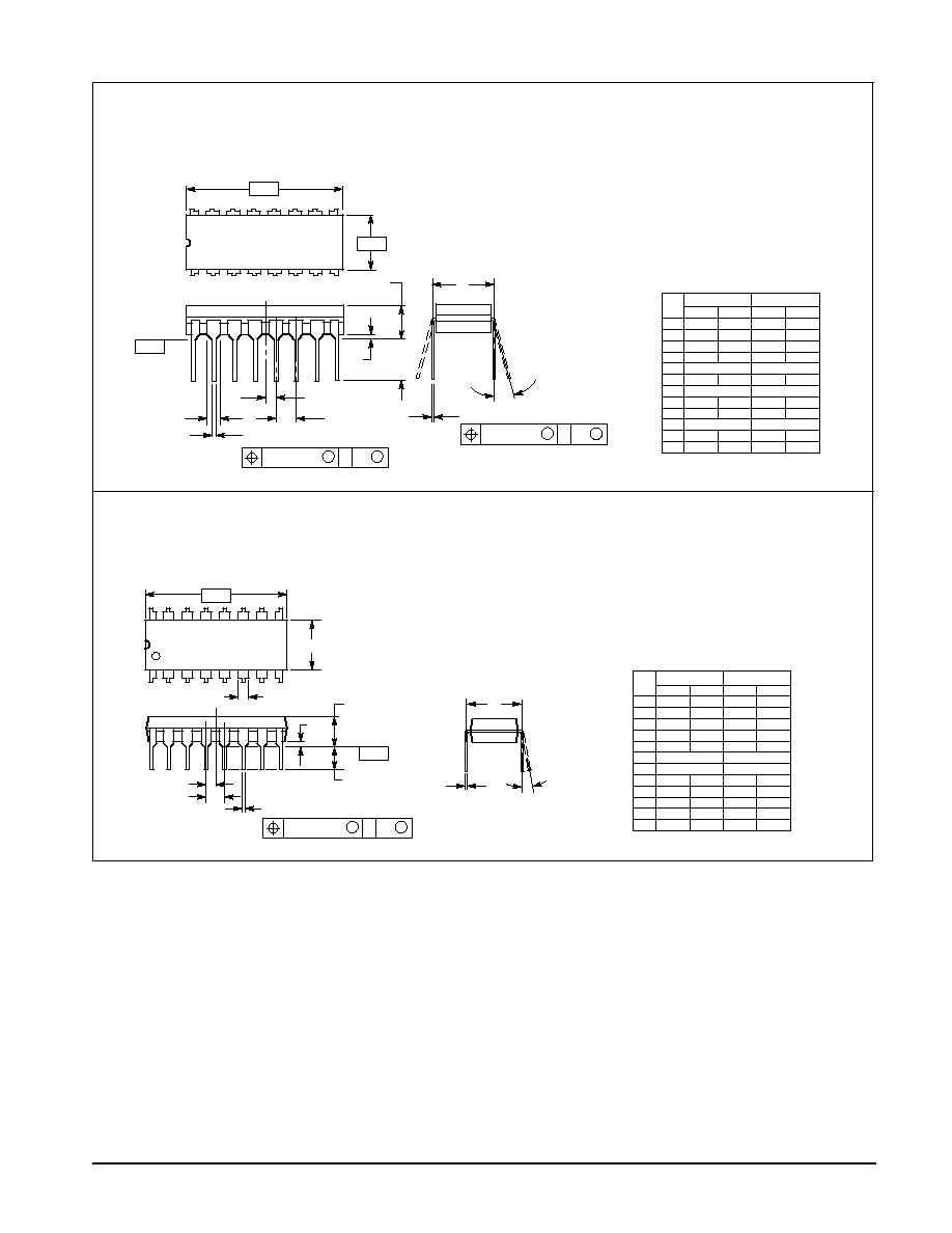
OUTLINE DIMENSIONS
P SUFFIX
PLASTIC DIP PACKAGE
CASE 648≠08
ISSUE R
NOTES:
1. DIMENSIONING AND TOLERANCING PER ANSI
Y14.5M, 1982.
2. CONTROLLING DIMENSION: INCH.
3. DIMENSION L TO CENTER OF LEADS WHEN
FORMED PARALLEL.
4. DIMENSION B DOES NOT INCLUDE MOLD FLASH.
5. ROUNDED CORNERS OPTIONAL.
≠A≠
B
F
C
S
H
G
D
J
L
M
16 PL
SEATING
1
8
9
16
K
PLANE
≠T≠
M
A
M
0.25 (0.010)
T
DIM
MIN
MAX
MIN
MAX
MILLIMETERS
INCHES
A
0.740
0.770
18.80
19.55
B
0.250
0.270
6.35
6.85
C
0.145
0.175
3.69
4.44
D
0.015
0.021
0.39
0.53
F
0.040
0.70
1.02
1.77
G
0.100 BSC
2.54 BSC
H
0.050 BSC
1.27 BSC
J
0.008
0.015
0.21
0.38
K
0.110
0.130
2.80
3.30
L
0.295
0.305
7.50
7.74
M
0
10
0
10
S
0.020
0.040
0.51
1.01
_
_
_
_
L SUFFIX
CERAMIC DIP PACKAGE
CASE 620≠10
ISSUE V
NOTES:
1. DIMENSIONING AND TOLERANCING PER
ANSI Y14.5M, 1982.
2. CONTROLLING DIMENSION: INCH.
3. DIMENSION L TO CENTER OF LEAD WHEN
FORMED PARALLEL.
4. DIMENSION F MAY NARROW TO 0.76 (0.030)
WHERE THE LEAD ENTERS THE CERAMIC
BODY.
≠A≠
≠B≠
≠T≠
F
E
G
N
K
C
SEATING
PLANE
16 PL
D
S
A
M
0.25 (0.010)
T
16 PL
J
S
B
M
0.25 (0.010)
T
M
L
DIM
MIN
MAX
MIN
MAX
MILLIMETERS
INCHES
A
0.750
0.785
19.05
19.93
B
0.240
0.295
6.10
7.49
C
≠≠≠
0.200
≠≠≠
5.08
D
0.015
0.020
0.39
0.50
E
0.050 BSC
1.27 BSC
F
0.055
0.065
1.40
1.65
G
0.100 BSC
2.54 BSC
H
0.008
0.015
0.21
0.38
K
0.125
0.170
3.18
4.31
L
0.300 BSC
7.62 BSC
M
0
15
0
15
N
0.020
0.040
0.51
1.01
_
_
_
_
16
9
1
8
MOTOROLA CMOS LOGIC DATA
MC14528B
8
OUTLINE DIMENSIONS
D SUFFIX
PLASTIC SOIC PACKAGE
CASE 751B≠05
ISSUE J
NOTES:
1. DIMENSIONING AND TOLERANCING PER ANSI
Y14.5M, 1982.
2. CONTROLLING DIMENSION: MILLIMETER.
3. DIMENSIONS A AND B DO NOT INCLUDE
MOLD PROTRUSION.
4. MAXIMUM MOLD PROTRUSION 0.15 (0.006)
PER SIDE.
5. DIMENSION D DOES NOT INCLUDE DAMBAR
PROTRUSION. ALLOWABLE DAMBAR
PROTRUSION SHALL BE 0.127 (0.005) TOTAL
IN EXCESS OF THE D DIMENSION AT
MAXIMUM MATERIAL CONDITION.
1
8
16
9
SEATING
PLANE
F
J
M
R
X 45
_
G
8 PL
P
≠B≠
≠A≠
M
0.25 (0.010)
B
S
≠T≠
D
K
C
16 PL
S
B
M
0.25 (0.010)
A
S
T
DIM
MIN
MAX
MIN
MAX
INCHES
MILLIMETERS
A
9.80
10.00
0.386
0.393
B
3.80
4.00
0.150
0.157
C
1.35
1.75
0.054
0.068
D
0.35
0.49
0.014
0.019
F
0.40
1.25
0.016
0.049
G
1.27 BSC
0.050 BSC
J
0.19
0.25
0.008
0.009
K
0.10
0.25
0.004
0.009
M
0
7
0
7
P
5.80
6.20
0.229
0.244
R
0.25
0.50
0.010
0.019
_
_
_
_
How to reach us:
USA/EUROPE/Locations Not Listed: Motorola Literature Distribution;
JAPAN: Nippon Motorola Ltd.; Tatsumi≠SPD≠JLDC, 6F Seibu≠Butsuryu≠Center,
P.O. Box 20912; Phoenix, Arizona 85036. 1≠800≠441≠2447 or 602≠303≠5454
3≠14≠2 Tatsumi Koto≠Ku, Tokyo 135, Japan. 03≠81≠3521≠8315
MFAX: RMFAX0@email.sps.mot.com ≠ TOUCHTONE 602≠244≠6609
ASIA/PACIFIC: Motorola Semiconductors H.K. Ltd.; 8B Tai Ping Industrial Park,
INTERNET: http://Design≠NET.com
51 Ting Kok Road, Tai Po, N.T., Hong Kong. 852≠26629298
Motorola reserves the right to make changes without further notice to any products herein. Motorola makes no warranty, representation or guarantee regarding
the suitability of its products for any particular purpose, nor does Motorola assume any liability arising out of the application or use of any product or circuit,
and specifically disclaims any and all liability, including without limitation consequential or incidental damages. "Typical" parameters which may be provided
in Motorola data sheets and/or specifications can and do vary in different applications and actual performance may vary over time. All operating parameters,
including "Typicals" must be validated for each customer application by customer's technical experts. Motorola does not convey any license under its patent
rights nor the rights of others. Motorola products are not designed, intended, or authorized for use as components in systems intended for surgical implant
into the body, or other applications intended to support or sustain life, or for any other application in which the failure of the Motorola product could create a
situation where personal injury or death may occur. Should Buyer purchase or use Motorola products for any such unintended or unauthorized application,
Buyer shall indemnify and hold Motorola and its officers, employees, subsidiaries, affiliates, and distributors harmless against all claims, costs, damages, and
expenses, and reasonable attorney fees arising out of, directly or indirectly, any claim of personal injury or death associated with such unintended or
unauthorized use, even if such claim alleges that Motorola was negligent regarding the design or manufacture of the part. Motorola and
are registered
trademarks of Motorola, Inc. Motorola, Inc. is an Equal Opportunity/Affirmative Action Employer.
MC14528B/D
*MC14528B/D*