
WWW.MOTOROLA.COM/SEMICONDUCTORS
M68HC11
Microcontrollers
MC68HC11P2/D
Rev. 1, 4/2002
MC68HC11P2
Technical Data
MC68HC711P2


MC68HC11P2 -- Rev 1.0
Technical Data
MOTOROLA
3
MC68HC11P2
MC68HC711P2
Technical Data -- Rev 1.0
Motorola reserves the right to make changes without further notice to any products
herein. Motorola makes no warranty, representation or guarantee regarding the
suitability of its products for any particular purpose, nor does Motorola assume any
liability arising out of the application or use of any product or circuit, and specifically
disclaims any and all liability, including without limitation consequential or incidental
damages. "Typical" parameters which may be provided in Motorola data sheets and/or
specifications can and do vary in different applications and actual performance may
vary over time. All operating parameters, including "Typicals" must be validated for
each customer application by customer's technical experts. Motorola does not convey
any license under its patent rights nor the rights of others. Motorola products are not
designed, intended, or authorized for use as components in systems intended for
surgical implant into the body, or other applications intended to support or sustain life,
or for any other application in which the failure of the Motorola product could create a
situation where personal injury or death may occur. Should Buyer purchase or use
Motorola products for any such unintended or unauthorized application, Buyer shall
indemnify and hold Motorola and its officers, employees, subsidiaries, affiliates, and
distributors harmless against all claims, costs, damages, and expenses, and
reasonable attorney fees arising out of, directly or indirectly, any claim of personal
injury or death associated with such unintended or unauthorized use, even if such claim
alleges that Motorola was negligent regarding the design or manufacture of the part.
Motorola, Inc. is an Equal Opportunity/Affirmative Action Employer.
Motorola and
are registered trademarks of Motorola, Inc.
DigitalDNA is a trademark of Motorola, Inc.
© Motorola, Inc., 2002

Technical Data
MC68HC11P2 -- Rev 1.0
4
MOTOROLA

MC68HC11P2 -- Rev 1.0
Technical Data
MOTOROLA
List of Paragraphs
5
Technical Data -- MC68HC11P2
List of Paragraphs
List of Paragraphs. . . . . . . . . . . . . . . . . . . . . . . . . . . . . . . . 5
Table of Contents . . . . . . . . . . . . . . . . . . . . . . . . . . . . . . . . 7
List of Figures . . . . . . . . . . . . . . . . . . . . . . . . . . . . . . . . . . 13
List of Tables . . . . . . . . . . . . . . . . . . . . . . . . . . . . . . . . . . . 15
Section 1. General Description . . . . . . . . . . . . . . . . . . . . 17
Section 2. Pin Descriptions . . . . . . . . . . . . . . . . . . . . . . . 21
Section 3. Operating Modes and On-Chip Memory . . . . 41
Section 4. Parallel Input/Output . . . . . . . . . . . . . . . . . . . . 73
Section 5. Serial Communications Interface (SCI) . . . . . 87
Section 6. Motorola Interconnect Bus (MI BUS). . . . . . 109
Section 7. Serial Peripheral Interface (SPI). . . . . . . . . . 125
Section 8. Timing System. . . . . . . . . . . . . . . . . . . . . . . . 137
Section 9. Analog-to-Digital Converter . . . . . . . . . . . . . 173
Section 10. Resets and Interrupts . . . . . . . . . . . . . . . . . 185
Section 11. CPU Core and Instruction Set . . . . . . . . . . 213
Section 12. Electrical Specifications . . . . . . . . . . . . . . . 231
Section 13. Mechanical Data . . . . . . . . . . . . . . . . . . . . . 247
Section 14. Ordering Information . . . . . . . . . . . . . . . . . 251
Section 15. Development Support . . . . . . . . . . . . . . . . . 253
Glossary . . . . . . . . . . . . . . . . . . . . . . . . . . . . . . . . . . . . . . 255

List of Paragraphs
Technical Data
MC68HC11P2 -- Rev 1.0
6
List of Paragraphs
MOTOROLA
Revision History . . . . . . . . . . . . . . . . . . . . . . . . . . . . . . . 265

MC68HC11P2 -- Rev 1.0
Technical Data
MOTOROLA
Table of Contents
7
Technical Data -- MC68HC11P2
Table of Contents
List of Paragraphs
Table of Contents
List of Figures
List of Tables
Section 1. General Description
1.1
Contents . . . . . . . . . . . . . . . . . . . . . . . . . . . . . . . . . . . . . . . . . . 17
1.2
Introduction . . . . . . . . . . . . . . . . . . . . . . . . . . . . . . . . . . . . . . . . 17
1.3
Features . . . . . . . . . . . . . . . . . . . . . . . . . . . . . . . . . . . . . . . . . . 18
Section 2. Pin Descriptions
2.1
Contents . . . . . . . . . . . . . . . . . . . . . . . . . . . . . . . . . . . . . . . . . . 21
2.2
Introduction . . . . . . . . . . . . . . . . . . . . . . . . . . . . . . . . . . . . . . . . 21
2.3
VDD and VSS . . . . . . . . . . . . . . . . . . . . . . . . . . . . . . . . . . . . . . 22
2.4
RESET . . . . . . . . . . . . . . . . . . . . . . . . . . . . . . . . . . . . . . . . . . . 23
2.5
Crystal driver and external clock input (XTAL, EXTAL) . . . . . .24
2.6
E clock output (E) . . . . . . . . . . . . . . . . . . . . . . . . . . . . . . . . . . . 26
2.7
Phase-locked loop (XFC, VDDSYN). . . . . . . . . . . . . . . . . . . . . 26
2.8
Interrupt request (IRQ) . . . . . . . . . . . . . . . . . . . . . . . . . . . . . . . 32
2.9
Nonmaskable interrupt (XIRQ/VPPE). . . . . . . . . . . . . . . . . . . . 32
2.10
MODA and MODB (MODA/LIR and MODB/VSTBY) . . . . . . . . 33

Table of Contents
Technical Data
MC68HC11P2 -- Rev 1.0
8
Table of Contents
MOTOROLA
2.11
VRH and VRL . . . . . . . . . . . . . . . . . . . . . . . . . . . . . . . . . . . . . . 34
2.12
PG7/R/W. . . . . . . . . . . . . . . . . . . . . . . . . . . . . . . . . . . . . . . . . . 34
2.13
Port signals . . . . . . . . . . . . . . . . . . . . . . . . . . . . . . . . . . . . . . . . 34
Section 3. Operating Modes and On-Chip Memory
3.1
Contents . . . . . . . . . . . . . . . . . . . . . . . . . . . . . . . . . . . . . . . . . . 41
3.2
Introduction . . . . . . . . . . . . . . . . . . . . . . . . . . . . . . . . . . . . . . . . 41
3.3
Operating modes . . . . . . . . . . . . . . . . . . . . . . . . . . . . . . . . . . . 41
3.4
On-chip memory . . . . . . . . . . . . . . . . . . . . . . . . . . . . . . . . . . . . 44
3.5
System initialization . . . . . . . . . . . . . . . . . . . . . . . . . . . . . . . . . 51
3.6
EPROM, EEPROM and CONFIG register . . . . . . . . . . . . . . . . 64
Section 4. Parallel Input/Output
4.1
Contents . . . . . . . . . . . . . . . . . . . . . . . . . . . . . . . . . . . . . . . . . . 73
4.2
Introduction . . . . . . . . . . . . . . . . . . . . . . . . . . . . . . . . . . . . . . . . 73
4.3
Port A . . . . . . . . . . . . . . . . . . . . . . . . . . . . . . . . . . . . . . . . . . . . 74
4.4
Port B . . . . . . . . . . . . . . . . . . . . . . . . . . . . . . . . . . . . . . . . . . . . 75
4.5
Port C . . . . . . . . . . . . . . . . . . . . . . . . . . . . . . . . . . . . . . . . . . . . 77
4.6
Port D . . . . . . . . . . . . . . . . . . . . . . . . . . . . . . . . . . . . . . . . . . . . 78
4.7
Port E . . . . . . . . . . . . . . . . . . . . . . . . . . . . . . . . . . . . . . . . . . . . 79
4.8
Port F . . . . . . . . . . . . . . . . . . . . . . . . . . . . . . . . . . . . . . . . . . . . 80
4.9
Port G . . . . . . . . . . . . . . . . . . . . . . . . . . . . . . . . . . . . . . . . . . . .81
4.10
Port H . . . . . . . . . . . . . . . . . . . . . . . . . . . . . . . . . . . . . . . . . . . . 82
4.11
Internal pull-up/pull-down resistors . . . . . . . . . . . . . . . . . . . . . . 83
4.12
System configuration . . . . . . . . . . . . . . . . . . . . . . . . . . . . . . . . 84

Table of Contents
MC68HC11P2 -- Rev 1.0
Technical Data
MOTOROLA
Table of Contents
9
Section 5. Serial Communications Interface (SCI)
5.1
Contents . . . . . . . . . . . . . . . . . . . . . . . . . . . . . . . . . . . . . . . . . . 87
5.2
Introduction . . . . . . . . . . . . . . . . . . . . . . . . . . . . . . . . . . . . . . . . 87
5.3
Data format . . . . . . . . . . . . . . . . . . . . . . . . . . . . . . . . . . . . . . . . 88
5.4
Transmit operation . . . . . . . . . . . . . . . . . . . . . . . . . . . . . . . . . .89
5.5
Receive operation. . . . . . . . . . . . . . . . . . . . . . . . . . . . . . . . . . . 89
5.6
Wakeup feature . . . . . . . . . . . . . . . . . . . . . . . . . . . . . . . . . . . . 91
5.7
SCI error detection . . . . . . . . . . . . . . . . . . . . . . . . . . . . . . . . . .92
5.8
SCI registers . . . . . . . . . . . . . . . . . . . . . . . . . . . . . . . . . . . . . . . 93
5.9
Status flags and interrupts . . . . . . . . . . . . . . . . . . . . . . . . . . . 101
5.10
Additional SCI subsystems . . . . . . . . . . . . . . . . . . . . . . . . . . . 104
Section 6. Motorola Interconnect Bus (MI BUS)
6.1
Contents . . . . . . . . . . . . . . . . . . . . . . . . . . . . . . . . . . . . . . . . . 109
6.2
Introduction . . . . . . . . . . . . . . . . . . . . . . . . . . . . . . . . . . . . . . . 109
6.3
Push-pull sequence . . . . . . . . . . . . . . . . . . . . . . . . . . . . . . . . 111
6.4
The push field . . . . . . . . . . . . . . . . . . . . . . . . . . . . . . . . . . . . . 112
6.5
The pull field . . . . . . . . . . . . . . . . . . . . . . . . . . . . . . . . . . . . . . 112
6.6
Biphase coding . . . . . . . . . . . . . . . . . . . . . . . . . . . . . . . . . . . .113
6.7
Message validation . . . . . . . . . . . . . . . . . . . . . . . . . . . . . . . . . 113
6.8
Interfacing to MI BUS . . . . . . . . . . . . . . . . . . . . . . . . . . . . . . . 116
6.9
MI BUS clock rate . . . . . . . . . . . . . . . . . . . . . . . . . . . . . . . . . . 117
6.10
SCI/MI BUS2 registers . . . . . . . . . . . . . . . . . . . . . . . . . . . . . . 117
6.11
SCI/MI BUS3 registers . . . . . . . . . . . . . . . . . . . . . . . . . . . . . . 123

Table of Contents
Technical Data
MC68HC11P2 -- Rev 1.0
10
Table of Contents
MOTOROLA
Section 7. Serial Peripheral Interface (SPI)
7.1
Contents . . . . . . . . . . . . . . . . . . . . . . . . . . . . . . . . . . . . . . . . . 125
7.2
Introduction . . . . . . . . . . . . . . . . . . . . . . . . . . . . . . . . . . . . . . . 125
7.3
Functional description. . . . . . . . . . . . . . . . . . . . . . . . . . . . . . . 126
7.4
SPI transfer formats . . . . . . . . . . . . . . . . . . . . . . . . . . . . . . . . 126
7.5
SPI signals . . . . . . . . . . . . . . . . . . . . . . . . . . . . . . . . . . . . . . . 129
7.6
SPI system errors . . . . . . . . . . . . . . . . . . . . . . . . . . . . . . . . . . 130
7.7
SPI registers . . . . . . . . . . . . . . . . . . . . . . . . . . . . . . . . . . . . . . 132
Section 8. Timing System
8.1
Contents . . . . . . . . . . . . . . . . . . . . . . . . . . . . . . . . . . . . . . . . . 137
8.2
Introduction . . . . . . . . . . . . . . . . . . . . . . . . . . . . . . . . . . . . . . . 137
8.3
Timer structure . . . . . . . . . . . . . . . . . . . . . . . . . . . . . . . . . . . . 139
8.4
Input capture. . . . . . . . . . . . . . . . . . . . . . . . . . . . . . . . . . . . . . 142
8.5
Output compare . . . . . . . . . . . . . . . . . . . . . . . . . . . . . . . . . . . 145
8.6
Real-time interrupt . . . . . . . . . . . . . . . . . . . . . . . . . . . . . . . . .154
8.7
Computer operating properly watchdog function . . . . . . . . . . 157
8.8
Pulse accumulator . . . . . . . . . . . . . . . . . . . . . . . . . . . . . . . . .158
8.9
Pulse-width modulation (PWM) timer . . . . . . . . . . . . . . . . . . . 162
Section 9. Analog-to-Digital Converter
9.1
Contents . . . . . . . . . . . . . . . . . . . . . . . . . . . . . . . . . . . . . . . . . 173
9.2
Introduction . . . . . . . . . . . . . . . . . . . . . . . . . . . . . . . . . . . . . . . 173
9.3
Overview. . . . . . . . . . . . . . . . . . . . . . . . . . . . . . . . . . . . . . . . . 174
9.4
A/D converter power-up and clock select . . . . . . . . . . . . . . . . 178
9.5
Channel assignments . . . . . . . . . . . . . . . . . . . . . . . . . . . . . . . 180
9.6
Control, status and results registers . . . . . . . . . . . . . . . . . . . . 181

Table of Contents
MC68HC11P2 -- Rev 1.0
Technical Data
MOTOROLA
Table of Contents
11
9.7
Operation in STOP and WAIT modes. . . . . . . . . . . . . . . . . . . 184
Section 10. Resets and Interrupts
10.1
Contents . . . . . . . . . . . . . . . . . . . . . . . . . . . . . . . . . . . . . . . . . 185
10.2
Introduction . . . . . . . . . . . . . . . . . . . . . . . . . . . . . . . . . . . . . . . 185
10.3
Resets. . . . . . . . . . . . . . . . . . . . . . . . . . . . . . . . . . . . . . . . . . .185
10.4
Effects of reset . . . . . . . . . . . . . . . . . . . . . . . . . . . . . . . . . . . . 192
10.5
Reset and interrupt priority . . . . . . . . . . . . . . . . . . . . . . . . . . . 195
10.6
Interrupts. . . . . . . . . . . . . . . . . . . . . . . . . . . . . . . . . . . . . . . . . 200
10.7
Low power operation . . . . . . . . . . . . . . . . . . . . . . . . . . . . . . . 203
Section 11. CPU Core and Instruction Set
11.1
Contents . . . . . . . . . . . . . . . . . . . . . . . . . . . . . . . . . . . . . . . . . 213
11.2
Introduction . . . . . . . . . . . . . . . . . . . . . . . . . . . . . . . . . . . . . . . 213
11.3
Registers. . . . . . . . . . . . . . . . . . . . . . . . . . . . . . . . . . . . . . . . . 214
11.4
Data types. . . . . . . . . . . . . . . . . . . . . . . . . . . . . . . . . . . . . . . . 220
11.5
Opcodes and operands . . . . . . . . . . . . . . . . . . . . . . . . . . . . . 220
11.6
Addressing modes . . . . . . . . . . . . . . . . . . . . . . . . . . . . . . . . .221
11.7
Instruction set . . . . . . . . . . . . . . . . . . . . . . . . . . . . . . . . . . . . . 223
Section 12. Electrical Specifications
12.1
Contents . . . . . . . . . . . . . . . . . . . . . . . . . . . . . . . . . . . . . . . . . 231
12.2
Introduction . . . . . . . . . . . . . . . . . . . . . . . . . . . . . . . . . . . . . . . 231
12.3
Maximum ratings . . . . . . . . . . . . . . . . . . . . . . . . . . . . . . . . . . 232
12.4
Thermal characteristics and power considerations. . . . . . . . . 233
12.5
Test methods . . . . . . . . . . . . . . . . . . . . . . . . . . . . . . . . . . . . . 234
12.6
DC electrical characteristics . . . . . . . . . . . . . . . . . . . . . . . . . . 235

Table of Contents
Technical Data
MC68HC11P2 -- Rev 1.0
12
Table of Contents
MOTOROLA
12.7
Control timing . . . . . . . . . . . . . . . . . . . . . . . . . . . . . . . . . . . . . 237
Section 13. Mechanical Data
13.1
Contents . . . . . . . . . . . . . . . . . . . . . . . . . . . . . . . . . . . . . . . . . 247
13.2
Pin assignments . . . . . . . . . . . . . . . . . . . . . . . . . . . . . . . . . . . 248
13.3
Package dimensions. . . . . . . . . . . . . . . . . . . . . . . . . . . . . . . . 249
Section 14. Ordering Information
14.1
Contents . . . . . . . . . . . . . . . . . . . . . . . . . . . . . . . . . . . . . . . . . 251
14.2
Introduction . . . . . . . . . . . . . . . . . . . . . . . . . . . . . . . . . . . . . . . 251
Section 15. Development Support
15.1
Contents . . . . . . . . . . . . . . . . . . . . . . . . . . . . . . . . . . . . . . . . . 253
15.2
Introduction . . . . . . . . . . . . . . . . . . . . . . . . . . . . . . . . . . . . . . . 253
15.3
EVS -- Evaluation system . . . . . . . . . . . . . . . . . . . . . . . . . . . 253
Glossary
Revision History
15.4
Major Changes Between Revision 1.0 and Revision 0.0 . . . . 265

MC68HC11P2 -- Rev 1.0
Technical Data
MOTOROLA
List of Figures
13
Technical Data -- MC68HC11P2
List of Figures
Figure
Title
Page
1-1
MC68HC11P2/MC68HC711P2 block diagram . . . . . . . . . . . . . 19
2-1
84-pin PLCC/CERQUAD pinout . . . . . . . . . . . . . . . . . . . . . . . . 22
2-2
External reset circuitry . . . . . . . . . . . . . . . . . . . . . . . . . . . . . . . 24
2-3
Oscillator connections. . . . . . . . . . . . . . . . . . . . . . . . . . . . . . . . 25
2-4
PLL circuit . . . . . . . . . . . . . . . . . . . . . . . . . . . . . . . . . . . . . . . . . 27
2-5
RAM stand-by connections. . . . . . . . . . . . . . . . . . . . . . . . . . . . 33
3-1
MC68HC11P2 memory map. . . . . . . . . . . . . . . . . . . . . . . . . . . 44
3-2
RAM and register overlap . . . . . . . . . . . . . . . . . . . . . . . . . . . . . 57
5-1
SCI baud rate generator circuit diagram. . . . . . . . . . . . . . . . . . 88
5-2
SCI1 block diagram . . . . . . . . . . . . . . . . . . . . . . . . . . . . . . . . . 90
5-3
Interrupt source resolution within SCI. . . . . . . . . . . . . . . . . . . 103
6-1
MI BUS timing. . . . . . . . . . . . . . . . . . . . . . . . . . . . . . . . . . . . . 111
6-2
Biphase coding and error detection . . . . . . . . . . . . . . . . . . . . 113
6-3
MI BUS block diagram . . . . . . . . . . . . . . . . . . . . . . . . . . . . . . 115
6-4
A typical interface between the MC68HC11P2 and the MI BUS
. . . . . . . . . . . . . . . . . . . . . . . . . . . . . . . . . . . . . . . . . . . . . . . . 116
7-1
SPI block diagram. . . . . . . . . . . . . . . . . . . . . . . . . . . . . . . . . . 127
7-2
SPI transfer format . . . . . . . . . . . . . . . . . . . . . . . . . . . . . . . . .128
8-1
Timer clock divider chains . . . . . . . . . . . . . . . . . . . . . . . . . . . 140
8-2
Capture/compare block diagram. . . . . . . . . . . . . . . . . . . . . . . 141
8-3
Pulse accumulator block diagram. . . . . . . . . . . . . . . . . . . . . .159
8-4
PWM timer block diagram. . . . . . . . . . . . . . . . . . . . . . . . . . . . 164
8-5
PWM duty cycle . . . . . . . . . . . . . . . . . . . . . . . . . . . . . . . . . . . 170
9-1
A/D converter block diagram . . . . . . . . . . . . . . . . . . . . . . . . . 174
9-2
Electrical model of an A/D input pin (in sample mode) . . . . . . 175
9-3
A/D conversion sequence. . . . . . . . . . . . . . . . . . . . . . . . . . . . 177
10-1
Processing flow out of reset (1 of 2) . . . . . . . . . . . . . . . . . . . . 206
10-2
Processing flow out of reset (2 of 2) . . . . . . . . . . . . . . . . . . . . 207
10-3
Interrupt priority resolution (1 of 3) . . . . . . . . . . . . . . . . . . . . . 208

List of Figures
Technical Data
MC68HC11P2 -- Rev 1.0
14
List of Figures
MOTOROLA
10-4
Interrupt priority resolution (2 of 3) . . . . . . . . . . . . . . . . . . . . . 209
10-5
Interrupt priority resolution (3 of 3) . . . . . . . . . . . . . . . . . . . . . 210
10-6
Interrupt source resolution within the SCI subsystem. . . . . . . 211
11-1
Programming model . . . . . . . . . . . . . . . . . . . . . . . . . . . . . . . . 214
11-2
Stacking operations . . . . . . . . . . . . . . . . . . . . . . . . . . . . . . . . 216
12-1
Test methods . . . . . . . . . . . . . . . . . . . . . . . . . . . . . . . . . . . . . 234
12-2
Timer inputs . . . . . . . . . . . . . . . . . . . . . . . . . . . . . . . . . . . . . . 237
12-3
Reset timing . . . . . . . . . . . . . . . . . . . . . . . . . . . . . . . . . . . . . . 238
12-4
Interrupt timing . . . . . . . . . . . . . . . . . . . . . . . . . . . . . . . . . . . . 238
12-5
STOP recovery timing. . . . . . . . . . . . . . . . . . . . . . . . . . . . . . . 239
12-6
WAIT recovery timing . . . . . . . . . . . . . . . . . . . . . . . . . . . . . . . 239
12-7
Port read timing diagram . . . . . . . . . . . . . . . . . . . . . . . . . . . . 240
12-8
Port write timing diagram . . . . . . . . . . . . . . . . . . . . . . . . . . . . 240
12-9
SPI master timing (CPHA = 0) . . . . . . . . . . . . . . . . . . . . . . . . 243
12-10 SPI master timing (CPHA = 1) . . . . . . . . . . . . . . . . . . . . . . . . 243
12-11 SPI slave timing (CPHA = 0) . . . . . . . . . . . . . . . . . . . . . . . . . 244
12-12 SPI slave timing (CPHA = 1) . . . . . . . . . . . . . . . . . . . . . . . . . 244
12-13 Expansion bus timing . . . . . . . . . . . . . . . . . . . . . . . . . . . . . . . 246
13-1
84-pin PLCC/CERQUAD pinout . . . . . . . . . . . . . . . . . . . . . . . 248
13-2
84-pin PLCC mechanical dimensions. . . . . . . . . . . . . . . . . . . 249
13-3
84-pin CERQUAD mechanical dimensions . . . . . . . . . . . . . . 250

MC68HC11P2 -- Rev 1.0
Technical Data
MOTOROLA
List of Tables
15
Technical Data -- MC68HC11P2
List of Tables
Table
Title
Page
2-1
Port signal functions . . . . . . . . . . . . . . . . . . . . . . . . . . . . . . . . . 35
3-1
Example bootloader baud rates . . . . . . . . . . . . . . . . . . . . . . . . 43
3-2
Register and control bit assignments . . . . . . . . . . . . . . . . . . . .47
3-3
Registers with limited write access . . . . . . . . . . . . . . . . . . . . . . 51
3-4
Hardware mode select summary . . . . . . . . . . . . . . . . . . . . . . . 53
3-5
RAM and register remapping . . . . . . . . . . . . . . . . . . . . . . . . . . 56
3-6
EEPROM remapping . . . . . . . . . . . . . . . . . . . . . . . . . . . . . . . . 58
3-7
EEPROM block protect. . . . . . . . . . . . . . . . . . . . . . . . . . . . . . . 62
3-8
Erase mode selection . . . . . . . . . . . . . . . . . . . . . . . . . . . . . . . . 67
4-1
Port configuration . . . . . . . . . . . . . . . . . . . . . . . . . . . . . . . . . . . 74
5-1
Example SCI baud rate control values . . . . . . . . . . . . . . . . . . . 95
7-1
SPI clock rates . . . . . . . . . . . . . . . . . . . . . . . . . . . . . . . . . . . . 133
8-1
Timer resolution and capacity. . . . . . . . . . . . . . . . . . . . . . . . . 139
8-2
RTI periodic rates . . . . . . . . . . . . . . . . . . . . . . . . . . . . . . . . . . 154
8-3
Pulse accumulator timing . . . . . . . . . . . . . . . . . . . . . . . . . . . . 158
8-4
Clock A and clock B prescalers . . . . . . . . . . . . . . . . . . . . . . . 167
9-1
A/D converter channel assignments . . . . . . . . . . . . . . . . . . . . 180
10-1
COP timer rate select . . . . . . . . . . . . . . . . . . . . . . . . . . . . . . . 187
10-2
Reset cause, reset vector and operating mode . . . . . . . . . . . 192
10-3
Highest priority interrupt selection . . . . . . . . . . . . . . . . . . . . . 198
10-4
Interrupt and reset vector assignments . . . . . . . . . . . . . . . . . 199
10-5
Stacking order on entry to interrupts. . . . . . . . . . . . . . . . . . . . 201
11-1
Reset vector comparison . . . . . . . . . . . . . . . . . . . . . . . . . . . . 217
11-2
Instruction set . . . . . . . . . . . . . . . . . . . . . . . . . . . . . . . . . . . . . 223
14-1
Ordering information . . . . . . . . . . . . . . . . . . . . . . . . . . . . . . . . 251
15-1
M68HC11 development tools . . . . . . . . . . . . . . . . . . . . . . . . . 253

List of Tables
Technical Data
MC68HC11P2 -- Rev 1.0
16
List of Tables
MOTOROLA

MC68HC11P2 -- Rev 1.0
Technical Data
MOTOROLA
General Description
17
Technical Data -- MC68HC11P2
Section 1. General Description
1.1 Contents
1.2
Introduction. . . . . . . . . . . . . . . . . . . . . . . . . . . . . . . . . . . . . . . 17
1.3
Features. . . . . . . . . . . . . . . . . . . . . . . . . . . . . . . . . . . . . . . . . . 18
1.2 Introduction
The MC68HC11P2 8-bit microcomputer is a member of the M68HC11
family of HCMOS microcomputers. In addition to 32kbytes of ROM, the
MC68HC11P2 contains 1kbyte of RAM and 640 bytes of EEPROM. With
its advanced timer and communication features (including MI BUS
(1)
)
the MC68HC11P2 is especially suitable for mobile communications and
automotive applications.
The MC68HC711P2 is an EPROM version of the MC68HC11P2, with
the User ROM replaced by a similar amount of EPROM. All references
to the MC68HC11P2 apply equally to the MC68HC711P2, unless
otherwise noted. References specific to the MC68HC711P2 are
italicised in the text.
1. The Motorola interconnect bus (MI BUS) is a serial communications protocol which supports
distributed real-time control efficiently and with a high degree of noise immunity. It allows data
to be transferred between the MCU and the slave device using only one wire, making this type
of communication suitable for medium speed networks requiring very low cost multiplex wir-
ing.

General Description
Technical Data
MC68HC11P2 -- Rev 1.0
18
General Description
MOTOROLA
1.3 Features
∑
Low power, high performance M68HC11 CPU core, with 4MHz
bus capability
∑
Power saving PLL clock circuit, with automatic disable during
WAIT mode
∑
32kbytes of User ROM (MC68HC11P2); 32kbytes User EPROM
(MC68HC711P2)
∑
1kbyte of RAM
∑
640 bytes of byte-erasable User EEPROM, with on-chip charge
pump
∑
Up to 50 general purpose I/O lines, plus up to 12 input-only lines
∑
Non-multiplexed address and data buses, permitting direct access
to the full 64k address map
∑
16-bit timer with 3/4 input captures and 4/5 output compares;
pulse accumulator and COP watchdog timer
∑
Three 8- or 9-bit SCI subsystems, two with MI BUS
capability
∑
SPI subsystem, with software selectable MSB/LSB first option
∑
8-channel, 8-bit analog-to-digital (A/D) converter
∑
Four 8-bit PWM timer channels (may be concatenated to form
one, or two, 16-bit channels)
∑
Available in 84-pin PLCC or 84-pin CERQUAD packages

General Description
Features
MC68HC11P2 -- Rev 1.0
Technical Data
MOTOROLA
General Description
19
Figure 1-1. MC68HC11P2/MC68HC711P2 block diagram
PA7
PA6
PA5
PA4
PA2
PA1
PA0
PA3
PD5
PD4
PD3
PD2
PD1
PD0
PE7
PE6
PE5
PE4
PE2
PE1
PE0
PE3
PG7
PG6
PG5
PG4
PG2
PG1
PG0
PG3
PH7
PH6
PH5
PH4
PH2
PH1
PH0
PH3
OC1/PAI
OC1/OC2
OC1/OC3
OC1/OC4
IC4/OC1/OC5
IC1
IC2
IC3
Timer
COP watchdog
Periodic interrupt
Pulse accumulator
Port
A
Port
D
Por
t
E
Por
t
G
Po
r
t
H
SS
SCK
MOSI
MISO
SPI
SCI1+
TXD1
RXD1
VRH
VRL
AD7
AD6
AD5
AD4
AD3
AD2
AD1
AD0
8-channel
A/D
converter
PWM
PW4
PW3
PW2
PW1
Non-multiplexed address and data buses
Port B
Port F
Port C
A15
A14
A13
A12
A1
1
A10
A9
A8
A7
A6
A5
A4
A3
A2
A1
A0
D7
D6
D5
D4
D3
D2
D1
D0
PB7
PB6
PB5
PB4
PB3
PB2
PB1
PB0
PF7
PF6
PF5
PF4
PF3
PF2
PF1
PF0
PC7
PC6
PC5
PC4
PC3
PC2
PC1
PC0
VPPE/XIRQ
IRQ
RESET
LIR/MODA
VSTBY/MODB
Interrupts
&
mode
select
Oscillator
XTAL
EXTAL
E
XFC
VDD
VSS
5
5
640 bytes EEPROM
1 024 bytes RAM
M68HC11
CPU
PLL
VDDSYN
SCI2+
(with MI BUS)
TXD2
RXD2
ROM or EPROM
32768 x 8
(including 64 bytes for vectors)
R/W
SCI3+
(with MI BUS)
TXD3
RXD3

General Description
Technical Data
MC68HC11P2 -- Rev 1.0
20
General Description
MOTOROLA

MC68HC11P2 -- Rev 1.0
Technical Data
MOTOROLA
Pin Descriptions
21
Technical Data -- MC68HC11P2
Section 2. Pin Descriptions
2.1 Contents
2.2
Introduction. . . . . . . . . . . . . . . . . . . . . . . . . . . . . . . . . . . . . . . 21
2.3
VDD and VSS. . . . . . . . . . . . . . . . . . . . . . . . . . . . . . . . . . . . . . 22
2.4
RESET . . . . . . . . . . . . . . . . . . . . . . . . . . . . . . . . . . . . . . . . . . . 23
2.5
Crystal driver and external clock input (XTAL, EXTAL) . . . 24
2.6
E clock output (E) . . . . . . . . . . . . . . . . . . . . . . . . . . . . . . . . . . 26
2.7
Phase-locked loop (XFC, VDDSYN) . . . . . . . . . . . . . . . . . . . 26
2.8
Interrupt request (IRQ) . . . . . . . . . . . . . . . . . . . . . . . . . . . . . .32
2.9
Nonmaskable interrupt (XIRQ/VPPE) . . . . . . . . . . . . . . . . . . 32
2.10
MODA and MODB (MODA/LIR and MODB/VSTBY) . . . . . . . 33
2.11
VRH and VRL. . . . . . . . . . . . . . . . . . . . . . . . . . . . . . . . . . . . . . 34
2.12
PG7/R/W. . . . . . . . . . . . . . . . . . . . . . . . . . . . . . . . . . . . . . . . . . 34
2.13
Port signals . . . . . . . . . . . . . . . . . . . . . . . . . . . . . . . . . . . . . . . 34
2.2 Introduction
The MC68HC11P2 is available in an 84-pin plastic-leaded chip carrier
(PLCC); the MC68HC711P2 is also available in an 84-pin windowed
cerquad package, to allow full use of the EPROM. Most pins on this MCU
serve two or more functions, as described in the following paragraphs.
Refer to
Figure 2-1
which shows the pin assignments for both 84-pin
packages.

Pin Descriptions
Technical Data
MC68HC11P2 -- Rev 1.0
22
Pin Descriptions
MOTOROLA
2.3 VDD and VSS
Power is supplied to the microcontroller via these pins. VDD is the
positive supply and VSS is ground. The MCU operates from a single 5V
(nominal) power supply.
It is in the nature of CMOS designs that very fast signal transitions occur
on the MCU pins. These short rise and fall times place very high short-
duration current demands on the power supply. To prevent noise
problems, special care must be taken to provide good power supply
bypassing at the MCU. Bypass capacitors should have good high-
frequency characteristics and be as close to the MCU as possible.
Figure 2-1. 84-pin PLCC/CERQUAD pinout
PB0
/A8
PB1
/A9
PB2
/A10
PB3
/A1
1
PB4
/A12
PB5
/A13
PB6
/A14
PB7
/A15
VSS
VD
D
PA
0
/
I
C
3
PA
1
/
I
C
2
PA
2
/
I
C
1
P
A
3/OC
1/OC
5/IC
4
P
A
4/OC
1/OC
4
P
A
5/OC
1/OC
3
P
A
6/OC
1/OC
2
P
A
7/OC
1/P
A
I
PD
5/SS
PD
4/SC
K
PD
3/MOS
I
PG0
VD
D AD
AD
7/P
E
7
AD
6/P
E
6
AD
5/P
E
5
AD
4/P
E
4
AD
3/P
E
3
AD
2/P
E
2
AD
1/P
E
1
AD
0/P
E
0
VR
L
VRH
VSS AD
A7
/PF
7
A6
/PF
6
A5
/PF
5
A4
/PF
4
A3
/PF
3
A2
/PF
2
A1
/PF
1
A0
/PF
0
74
73
72
71
70
69
68
67
66
65
64
63
62
61
60
59
58
57
56
55
54
12
13
14
15
16
17
18
19
20
21
22
23
24
25
26
27
28
29
30
31
32
33
34
35
36
37
38
39
40
41
42
43
44
45
46
47
48
49
50
51
52
53
11
10
9
8
7
6
5
4
3
2
84
83
82
81
80
79
78
77
76
75
PD2/MISO
PD1/TXD1
PD0/RXD1
MODA/LIR
RESET
XFC
VDDSYN
EXTAL
XTAL
E
VDDR
VSSX
PC7/D7
PC6/D6
PC5/D5
PC4/D4
PC3/D3
PC2/D2
PC1/D1
PC0/D0
IRQ
PW1/PH0
PW2/PH1
PW3/PH2
PW4/PH3
RXD2/PH4
TXD2/PH5
RXD3/PH6
TXD3/PH7
MODB/VSTBY
XIRQ
VDD
VDDL
VSSX
VSS
R/W/PG7
PG6
PG5
PG4
PG3
PG2
PG1

Pin Descriptions
RESET
MC68HC11P2 -- Rev 1.0
Technical Data
MOTOROLA
Pin Descriptions
23
Bypassing requirements vary, depending on how heavily the MCU pins
are loaded.
The MC68HC11P2 MCU has five VDD pins and five VSS pins. One pair
of these pins is reserved for supplying power to the analog-to-digital
converter (VDD AD, VSS AD); two pairs are used for the internal logic
(VDD, VSS); the remaining two pairs supply power for the port logic on
either half of the chip (VDDL, VSSX and VDDR, VSSX). This
arrangement minimizes the injection of noise into the digital circuitry on
the chip.
2.4 RESET
An active low bidirectional control signal, RESET, acts as an input to
initialize the MCU to a known start-up state. It also acts as an open-drain
output to indicate that an internal failure has been detected in either the
clock monitor or the COP watchdog circuit. The CPU distinguishes
between internal and external reset conditions by sensing whether the
reset pin rises to a logic one in less than six E clock cycles after a reset
has occurred. It is therefore not advisable to connect an external
resistor-capacitor (RC) power-up delay circuit to the reset pin of
M68HC11 devices because the circuit charge time constant can cause
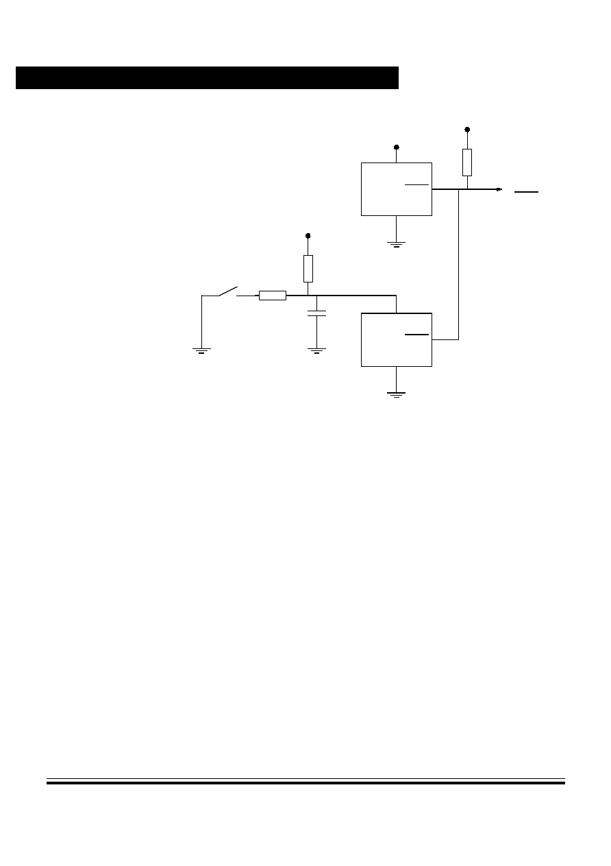
the device to misinterpret the type of reset that occurred. Refer to
Resets and Interrupts
for further information.
Figure 2-2
illustrates a typical reset circuit that includes an external
switch together with a low voltage inhibit circuit, to prevent power
transitions, or RAM or EEPROM corruption.
Pin Descriptions
Technical Data
MC68HC11P2 -- Rev 1.0
24
Pin Descriptions
MOTOROLA
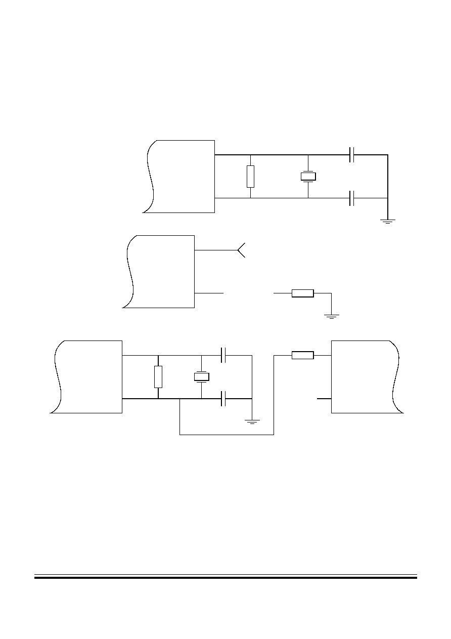
2.5 Crystal driver and external clock input (XTAL, EXTAL)
These two pins provide the interface for either a crystal or a CMOS
compatible clock to control the internal clock generator circuitry. The
frequency applied to these pins must be four times higher than the
desired E clock rate (unless the PLL circuit is used to provide the E
clock).
The XTAL pin is normally left unconnected when an external CMOS
compatible clock input is connected to the EXTAL pin. However, a 10 kæ
to 100 kæ load resistor connected from XTAL to ground can be used to
reduce RFI noise emission. The XTAL output is normally intended to
drive only a crystal. The XTAL output can be buffered with a high-
impedance buffer, or it can be used to drive the EXTAL input of another
M68HC11 family device.
Figure 2-2. External reset circuitry
V
DD
1µF
V
DD
4.7 kæ
To M68HC11
RESET
V
DD
1
2
3
1
2
3
IN
RESET
GND
IN
RESET
GND
MC34064
MC34164
Manual
reset
4.7 kæ
4.7 kæ
Pin Descriptions
Crystal driver and external clock input (XTAL, EXTAL)
MC68HC11P2 -- Rev 1.0
Technical Data
MOTOROLA
Pin Descriptions
25
In all cases, use caution when designing circuitry associated with the
oscillator pins. Load capacitances shown in the oscillator circuits include
all stray layout capacitances. See
Figure 2-3
.
Figure 2-3. Oscillator connections
10 Mæ
25 pF
4∑E
crystal
25 pF
EXTAL
XTAL
M68HC11
Note: capacitor values include all stray capacitance.
M68HC11
EXTAL
XTAL
NC or
10≠100kæ load
External oscillator
10 Mæ
25 pF
4∑E
crystal
25 pF
EXTAL
XTAL
M68HC11
M68HC11
EXTAL
XTAL
NC or
10≠100kæ
220æ
load
(a) Common crystal
connections
(b) External oscillator
connections
(c) One crystal driving two MCUs

Pin Descriptions
Technical Data
MC68HC11P2 -- Rev 1.0
26
Pin Descriptions
MOTOROLA
2.6 E clock output (E)
E is the output connection for the internally generated E clock. The signal
from E is used as a timing reference. The frequency of the E clock output
is one quarter that of the input frequency at the XTAL and EXTAL pins
(except when the PLL is used as the clock source). When E clock output
is low, an internal process is taking place; when it is high, data is being
accessed. All clocks, including the E clock, are halted when the MCU is
in STOP mode. The E clock output can be turned off in single chip
modes to reduce the effects of RFI.
2.7 Phase-locked loop (XFC, VDDSYN)
The XFC and VDDSYN pins are the inputs for the on-chip PLL (phase-
locked loop) circuitry. On reset all the device clocks are derived from the
EXTAL input. The EXTAL clock is used as a reference for the PLL circuit,
which generates a clock that is a multiple of the EXTAL frequency. Once
the PLL has stabilized, alternate clocks may be selected.
VDDSYN is the power supply pin for the PLL. Connecting it high enables
the internal low frequency oscillator circuitry designed for the PLL. The
PLL has been designed particularly for use with 614.4 and 640kHz
crystals, though other values may be used. The maximum
recommended crystal frequency for PLL operation is 2MHz. Above this
frequency VDDSYN should be grounded to disable the PLL and enable
the high frequency oscillator circuit; in this state EXTAL is designed for
16MHz operation and XFC may be left unconnected.
The PLL consists of a variable bandwidth loop filter, a voltage controlled
oscillator (VCO), a feedback frequency divider and a digital phase
detector. VDDSYN is the supply voltage for the PLL and must be suitably
bypassed. The external capacitor on XFC should be located as close to
the chip as possible to minimize noise. A typical value for this capacitor
is 0.047µF, for a crystal frequency of 614.4kHz.
(1)
1. In general, a larger capacitor will improve the PLL's frequency stability, at the expense of in-
creasing the time required for it to settle (t
PLLS
) at the desired frequency. For a 32kHz appli-
cation, or one in which the slew rate is not critical, a capacitor value of 0.1µF is usually
adequate. For a crystal frequency of 614.4kHz and a slew time of 1≠2ms (from 614kHz in
WAIT mode to 16MHz in RUN mode), a capacitor of 0.047µF has been found satisfactory.

Pin Descriptions
Phase-locked loop (XFC, VDDSYN)
MC68HC11P2 -- Rev 1.0
Technical Data
MOTOROLA
Pin Descriptions
27
The PLL filter has two bandwidths that are automatically selected by the
PLL, if the AUTO bit in PLLCR is set. Whenever the PLL is first enabled,
the wide bandwidth mode is used. This enables the PLL frequency to
ramp up quickly. When the output frequency is near the desired value,
the filter is switched to the narrow bandwidth mode, to make the final
frequency more stable. Manual control is possible, by clearing AUTO in
PLLCR, and setting the appropriate value for BWC.
A block diagram of the PLL circuitry is given in
Figure 2-4
.
2.7.1 Synchronization of PLL with subsystems
The timer and SCI subsystems operate off the EXTAL clock, but are
accessed by the CPU relative to the internal PH2 signal. Although the
EXTAL clock is used as the reference for the PLL, the PH2 clock and the
module clocks for the timer and the SCI are not synchronized. In order
to ensure synchronized data, special circuitry has been incorporated into
both subsystems.
Figure 2-4. PLL circuit
V
DDSYN
Bus clock
select
Module clock
select
Frequency divider
SYNR
Phase
detect
Loop filter
VCO
XFC
t
REF
PCOMP
t
FB
EXTAL
MCS
ST4XCK
4XCLK
BCS
EXTAL
EXTAL
Low frequency
crystal oscillator
To clock
generation
circuitry
For SCI
and timer
VCOOUT

Pin Descriptions
Technical Data
MC68HC11P2 -- Rev 1.0
28
Pin Descriptions
MOTOROLA
2.7.2 Changing the PLL frequency
To change the PLL frequency it is necessary to perform the following
sequence of events, in order to prevent possible bursts of high frequency
operation during the reconfiguration of the PLL:
1. Switch to the low frequency bus rate (BCS = 0)
2. Disable the PLL (PLLON = 0)
3. Change the value in SYNR
4. Enable the PLL (PLLON = 1)
5. Wait a time t
PLLS
for the PLL frequency to stabilize
6. Switch to the high frequency bus rate (BCS = 1)
2.7.3 PLL registers
Two registers are used to control the operation of the MC68HC11P2
phase-locked loop circuitry. These are the PLL control register and the
synthesizer program register, each of which is described below.
2.7.3.1 PLLCR -- PLL control register
This read/write register contains two bits that are used to enable and
disable the synthesizer and to switch from slow (EXTAL) to one of the
fast speeds. Two further bits are used to control the filter bandwidth. The
SCI and timer clock source and the slow clock for WAIT mode are also
controlled by this register.
PLLON -- PLL on
1 = Switch PLL on.
0 = Switch PLL off.
Address bit 7
bit 6
bit 5
bit 4
bit 3
bit 2
bit 1
bit 0
State
on reset
PLL control (PLLCR)
$002E PLLON BCS
AUTO BWC VCOT MCS
LCK
WEN 1010 1000

Pin Descriptions
Phase-locked loop (XFC, VDDSYN)
MC68HC11P2 -- Rev 1.0
Technical Data
MOTOROLA
Pin Descriptions
29
This bit activates the synthesizer circuit without connecting it to the
control circuit. This allows the circuit to stabilize before it drives the
CPU clocks. PLLON is set by reset, to allow the control loop to
stabilize during power up.
PLLON cannot be cleared whilst using VCOOUT to drive the internal
processor clock, i.e. when BCS is set.
BCS -- Bus clock select
1 = VCOOUT output drives the clock circuit (4XCLK).
0 = EXTAL drives the clock circuit (4XCLK).
This bit determines which signal drives the clock circuit generating the
bus clocks. Once BCS has been altered it can take up to [1.5 EXTAL
+ 1.5 VCOOUT] cycles for the change in the clock to occur. Reset
clears this bit.
NOTE:
PLLON and BCS have built-in safeguards so that VCOOUT cannot be
selected as the clock source (BCS = 1) if the PLL is off (PLLON = 0).
Similarly, the PLL cannot be turned off (PLLON = 0) if it is on and in use
(BCS = 1). Turning the PLL on and selecting VCOOUT as the clock
source therefore requires two independent writes to PLLCR.
AUTO -- Automatic bandwidth control
1 = Automatic bandwidth control selected.
0 = Manual bandwidth control selected.
AUTO selects between automatic bandwidth control circuits in the
phase detect block and manual bandwidth control. Reset sets this bit.
BWC -- Bandwidth control
1 = High bandwidth control selected.
0 = Low bandwidth control selected.
Bandwidth control is under manual control only when AUTO is clear.
(When AUTO is set, BWC acts as a read-only status bit to indicate
which mode has been selected by the internal circuit.) A delay of t
PLLS
is required between changes to BWC. The low bandwidth driver is
always enabled, so this bit determines whether the high bandwidth
driver is on or off. On PLL start-up in automatic mode (AUTO = 1), the
high bandwidth driver is enabled (BWC = 1) by internal circuitry until

Pin Descriptions
Technical Data
MC68HC11P2 -- Rev 1.0
30
Pin Descriptions
MOTOROLA
the PLL is near the specified frequency. The high bandwidth driver is
then disabled and BWC is cleared by internal circuitry. Reset clears
this bit.
VCOT -- VCO test (Test mode only)
1 = Loop filter operates as specified by AUTO and BWC.
0 = Low bandwidth mode of the PLL filter is disabled.
This bit is used to isolate the loop filter from the VCO for testing
purposes. VCOT is always set when AUTO = 1 when running in
automatic mode. This bit is writable only in test mode. Reset sets this
bit.
MCS -- Module clock select
1 = 4XCLK is the source for the SCI and timer divider chain.
0 = EXTAL is the source for the SCI and timer divider chain.
Reset clears this bit.
LCK -- Synthesizer lock detect
1 = The PLL has stabilized.
0 = The PLL is not stable.
This bit is used as an indicator for software that it is all right to set
BCS.
WEN -- WAIT enable
1 = Low-power WAIT mode selected (PLL set to `idle' in WAIT
mode).
0 = Do not alter the 4XCLK during WAIT mode.
This bit determines whether the 4XCLK is disconnected from
VCOOUT during WAIT and connected to EXTAL. Reset clears this
bit.
When set, the CPU will respond to a WAIT instruction by first stacking
the relevant registers, then by clearing BCS and setting the PLL to
`idle', with modulus = 1.
Auto
BWC
High
bandwidth
0
0
Off
0
1
On
1
X
Auto

Pin Descriptions
Phase-locked loop (XFC, VDDSYN)
MC68HC11P2 -- Rev 1.0
Technical Data
MOTOROLA
Pin Descriptions
31
Any interrupt, any reset, or the assertion of RAF in any of the SCIs will
allow the PLL to resume operating at the frequency specified in the
SYNR. The user must set BCS after the PLL has had time to adjust
(t
PLLS
). If, for a specific SCI, the RE bit is clear, then RAF cannot
become set, hence the PLL will not resume normal operation.
2.7.3.2 SYNR -- Synthesizer program register
The PLL frequency synthesizer multiplies the frequency of the crystal
oscillator. The multiplication factor is software programmable via a loop
divider, which consists of a six-bit modulo N counter, with a further two
bit scaling factor.
The multiplication factor is given by 2(Y + 1)2
X
, where 0 X 3 and 0
Y 63.
NOTE:
Exceeding recommended operating frequencies can result in
indeterminate MCU operation.
SYNX[1:0]
These bits program the binary taps (divide by 1, 2, 4 and 8). Reset
clears these bits.
SYNY[5:0]
These bits program the six-bit modulo N (1 to 64) counter. Reset sets
these bits to %001011.
NOTE:
The resolution of the multiplication factors decreases by a factor of two,
as X increases:
Address bit 7
bit 6
bit 5
bit 4
bit 3
bit 2
bit 1
bit 0
State
on reset
Synthesizer program (SYNR)
$002F SYNX1 SYNX0 SYNY5 SYNY4 SYNY3 SYNY2 SYNY1 SYNY0 0000 1011
X
Y
Possible multipliers
0
0 ≠ 63
2, 4, 6, 8, ..., 128
1
0 ≠ 63
4, 8, 12, 16, ..., 256
2
0 ≠ 63
8, 16, 24, 32, ..., 512
3
0 ≠ 63
16, 32, 48, 64, ..., 1024

Pin Descriptions
Technical Data
MC68HC11P2 -- Rev 1.0
32
Pin Descriptions
MOTOROLA
2.8 Interrupt request (IRQ)
The IRQ input provides a means of applying asynchronous interrupt
requests to the MCU. Either falling edge sensitive triggering or level
sensitive triggering is program selectable (OPTION register). IRQ is
always configured to level sensitive triggering at reset.
NOTE:
Connect an external pull-up resistor, typically 4.7 kæ, to V
DD
when IRQ
is used in a level sensitive wired-OR configuration. See also
Nonmaskable interrupt (XIRQ/VPPE)
.
2.9 Nonmaskable interrupt (XIRQ/VPPE)
The XIRQ input provides a means of requesting a non-maskable
interrupt after reset initialization. During reset, the X bit in the condition
code register (CCR) is set and any interrupt is masked until MCU
software enables it. Because the XIRQ input is level-sensitive, it can be
connected to a multiple-source wired-OR network with an external pull-
up resistor to V
DD
. XIRQ is often used as a power loss detect interrupt.
Whenever XIRQ or IRQ is used with multiple interrupt sources (IRQ
must be configured for level sensitive operation if there is more than one
source of IRQ interrupt), each source must drive the interrupt input with
an open-drain type of driver to avoid contention between outputs. There
should be a single pull-up resistor near the MCU interrupt input pin
(typically 4.7 kæ). There must also be an interlock mechanism at each
interrupt source so that the source holds the interrupt line low until the
MCU recognizes and acknowledges the interrupt request. If one or more
interrupt source is still pending after the MCU services a request, the
interrupt line will still be held low and the MCU will be interrupted again
as soon as the interrupt mask bit in the MCU is cleared (normally upon
return from an interrupt). Refer to
Resets and Interrupts
.
The VPPE pin is used to input the external EPROM programming
voltage, which must be present during EPROM programming.

Pin Descriptions
MODA and MODB (MODA/LIR and MODB/VSTBY)
MC68HC11P2 -- Rev 1.0
Technical Data
MOTOROLA
Pin Descriptions
33
2.10 MODA and MODB (MODA/LIR and MODB/VSTBY)
During reset, MODA and MODB select one of the four operating modes.
Refer to
Operating Modes and On-Chip Memory
.
After the operating mode has been selected, the LIR pin provides an
open-drain output to indicate that execution of an instruction has begun.
The LIR pin is normally configured for wired-OR operation (only pulls
low). In order to detect consecutive instructions in a high-speed
application, this signal can be made to drive high for a short time to
prevent false triggering. A series of E clock cycles occurs during
execution of each instruction. The LIR signal goes low during the first E
clock cycle of each instruction (opcode fetch). This output is provided for
assistance in program debugging and its operation is controlled by the
LIRDV bit in the OPT2 register.
The VSTBY pin is used to input RAM stand-by power. The MCU is
powered from the VDD pin unless the difference between the level of
VSTBY and VDD is greater than one MOS threshold (about 0.7 volts).
When these voltages differ by more than 0.7 volts, the internal 1024-byte
RAM and part of the reset logic are powered from VSTBY rather than
VDD. This allows RAM contents to be retained without VDD power
applied to the MCU. Reset must be driven low before V
DD
is removed
and must remain low until V
DD
has been restored to a valid level.
Figure 2-5. RAM stand-by connections
4.7kæ
(+)
4.8 V NiCd
V
DD
V
DD
V
OUT
V
BATT
MAX 690
To MODB/VSTBY
pin of M68HC11

Pin Descriptions
Technical Data
MC68HC11P2 -- Rev 1.0
34
Pin Descriptions
MOTOROLA
2.11 VRH and VRL
These pins provide the reference voltages for the analog-to-digital
converter.
2.12 PG7/R/W
This pin provides two separate functions, depending on the operating
mode. In single chip and bootstrap modes, PG7/R/W acts as
input/output port G bit 7. Refer to
Parallel Input/Output
for further
information.
In expanded and test modes, PG7/R/W performs the read/write function.
PG7/R/W signals the direction of transfers on the external data bus. A
high on this pin indicates that a read cycle is in progress.
2.13 Port signals
In the 84-pin PLCC package, 62 pins are arranged into seven 8-bit ports:
A, B, C, E, F, G, and H, and one six-bit port (D). The lines of ports A, B,
C, D, F, G, and H are fully bidirectional; E is input only. Each of the
bidirectional ports serves a purpose other than I/O, depending on the
operating mode or peripheral function selected. Note that ports B, C, F,
and one bit of port G are available for I/O functions only in single chip
and bootstrap modes. Refer to
Table 2-1
for details of the port signals'
functions in different operating modes.
NOTE:
When using the information about port functions, do not confuse pin
function with the electrical state of the pin at reset. All general-purpose
I/O pins configured as inputs at reset are in a high-impedance state. Port
data registers reflect the functional state of the port at reset. The pin
function is mode dependent.
Pin Descriptions
Port signals
MC68HC11P2 -- Rev 1.0
Technical Data
MOTOROLA
Pin Descriptions
35
2.13.1 Port A
Port A is an 8-bit general-purpose I/O port with a data register (PORTA)
and a data direction register (DDRA). Port A pins share functions with
the 16-bit timer system (see
Timing System
for further information).
PORTA can be read at any time: inputs return the pin level; outputs
return the pin driver input level. If written, PORTA stores the data in
internal latches. The pins are driven only if they are configured as
Table 2-1. Port signal functions
Port/bit
Single chip
and
bootstrap mode
Expanded multiplexed
and
special test mode
PA0
PA0/IC3
PA1
PA1/IC2
PA2
PA2/IC1
PA3
PA3/OC5/IC4 and/or OC1
PA4
PA4/OC4 and/or OC1
PA5
PA5/OC3 and/or OC1
PA6
PA6/OC2 and/or OC1
PA7
PA7/PAI and/or OC1
PB[7:0]
PB[7:0]
A[15:8]
PC[7:0]
PC[7:0]
D[7:0]
PD0
PD0/RXD1
PD1
PD1/TXD1
PD2
PD2/MISO
PD3
PD3/MOSI
PD4
PD4/SCK
PD5
PD5/SS
PE[7:0]
Input only or analog inputs
PF[7:0]
PF[7:0]
A[7:0]
PG[6:0]
PG[6:0]
PG7
PG7/R/W
PH0
PH0/PW1
PH1
PH1/PW2
PH2
PH2/PW3
PH3
PH3/PW4
PH4
PH4/RXD2
PH5
PH5/TXD2
PH6
PH6/RXD3
PH7
PH7/TXD3

Pin Descriptions
Technical Data
MC68HC11P2 -- Rev 1.0
36
Pin Descriptions
MOTOROLA
outputs. Writes to PORTA do not change the pin state when the pins are
configured for timer output compares.
Out of reset, port A pins [7:0] are general-purpose high-impedance
inputs. When the functions associated with these pins are disabled, the
bits in DDRA govern the I/O state of the associated pin. For further
information, refer to
Parallel Input/Output
.
2.13.2 Port B
Port B is an 8-bit general-purpose I/O port with a data register (PORTB)
and a data direction register (DDRB). In single chip mode, port B pins are
general-purpose I/O pins (PB[7:0]). In expanded mode, port B pins act
as the high-order address lines (A[15:8]) of the address bus.
PORTB can be read at any time: inputs return the pin level; outputs
return the pin driver input level. If PORTB is written, the data is stored in
internal latches. The pins are driven only if they are configured as
outputs in single chip or bootstrap mode. For further information, refer to
Parallel Input/Output
.
Port B pins include on-chip pull-up devices which can be enabled or
disabled.
2.13.3 Port C
Port C is an 8-bit general-purpose I/O port with a data register (PORTC)
and a data direction register (DDRC). In single chip mode, port C pins
are general-purpose I/O pins (PC[7:0]). In the expanded mode, port C
pins are configured as data bus pins (D[7:0]).
PORTC can be read at any time: inputs return the pin level; outputs
return the pin driver input level. If PORTC is written, the data is stored in
internal latches. The pins are driven only if they are configured as
outputs in single chip or bootstrap mode. Port C pins are general-
purpose inputs out of reset in single chip and bootstrap modes. In
expanded and test modes, these pins are data bus lines out of reset.

Pin Descriptions
Port signals
MC68HC11P2 -- Rev 1.0
Technical Data
MOTOROLA
Pin Descriptions
37
The CWOM control bit in the OPT2 register disables port C's P-channel
output drivers. Because the N-channel driver is not affected by CWOM,
setting CWOM causes port C to become an open-drain-type output port
suitable for wired-OR operation. In wired-OR mode (PORTC bits at logic
level zero), the pins are actively driven low by the N-channel driver.
When a port C bit is at logic level one, the associated pin is in a high
impedance state as neither the N-channel nor the P-channel devices are
active. It is customary to have an external pull-up resistor on lines that
are driven by open-drain devices. Port C can only be configured for
wired-OR operation when the MCU is in single chip mode. For further
information, refer to
Parallel Input/Output
.
2.13.4 Port D
Port D, a 6-bit general-purpose I/O port, has a data register (PORTD)
and a data direction register (DDRD). The six port D lines (D[5:0]) can
be used for general-purpose I/O, for one of the serial communications
interfaces (SCI1, bits [0:1]) and for the serial peripheral interface (SPI,
bits [2:5]) subsystem.
PORTD can be read at any time: inputs return the pin level; outputs
return the pin driver input level. If PORTD is written, the data is stored in
internal latches and are driven only if port D is configured for general-
purpose output.
For further information, refer to
Parallel Input/Output
,
Serial
Communications Interface (SCI)
and
Serial Peripheral Interface
(SPI)
.
2.13.5 Port E
Port E, PE/AD[7:0], is an input-only port that can also be used as the
analog inputs for the analog-to-digital converter.
For further information, refer to
Parallel Input/Output
and
Analog-to-
Digital Converter
.

Pin Descriptions
Technical Data
MC68HC11P2 -- Rev 1.0
38
Pin Descriptions
MOTOROLA
2.13.6 Port F
Port F is an 8-bit general-purpose I/O port with a data register (PORTF)
and a data direction register (DDRF). In single chip mode, port F pins are
general-purpose I/O pins (PF[7:0]). In expanded mode, port F pins act
as the low-order address lines (A[7:0]) of the address bus.
PORTF can be read at any time: inputs return the pin level; outputs
return the pin driver input level. If PORTF is written, the data is stored in
internal latches. The pins are driven only if they are configured as
outputs in single chip or bootstrap mode.
Port F pins include on-chip pull-up devices that can be enabled or
disabled.
For further information, refer to
Parallel Input/Output
.
2.13.7 Port G
In normal modes, Port G is an 8-bit general-purpose I/O port with a data
register (PORTG) and a data direction register (DDRG). Port G bit 7 is
the R/W line in expanded mode; the remaining bits are always general
purpose I/O.
PORTG can be read at any time: inputs return the pin level; outputs
return the pin driver input level. If PORTG is written, the data is stored in
internal latches.The pins are driven only if they are configured as outputs
in single chip or bootstrap mode. For further information, refer to
Parallel
Input/Output
.
Port G pins include on-chip pull-up devices that can be enabled or
disabled.
2.13.8 Port H
Port H is an 8-bit general-purpose I/O port with a data register (PORTH)
and a data direction register (DDRH). Port H pins support either
input/output, SCI2 (bits [7:6]), SCI3 (bits [5:4]), or pulse-width
modulation channels (bits [3:0]). Both of these SCI subsystems also
have MI BUS capability.

Pin Descriptions
Port signals
MC68HC11P2 -- Rev 1.0
Technical Data
MOTOROLA
Pin Descriptions
39
PORTH can be read at any time: inputs return the pin level; outputs
return the pin driver input level. If PORTH is written, the data is stored in
internal latches. The pins are driven only if they are configured as
outputs in single chip or bootstrap mode.
Port H pins include on-chip pull-up or pull-down devices that can be
enabled or disabled via the Port pull-up assignment register (PPAR).
Port H [7:4] have pull-up resistors; port H [3:0] have pull-down resistors.
For further information, refer to
Parallel Input/Output
,
Serial
Communications Interface (SCI)
,
Motorola Interconnect Bus
(MI BUS)
and
Timing System
.

Pin Descriptions
Technical Data
MC68HC11P2 -- Rev 1.0
40
Pin Descriptions
MOTOROLA

MC68HC11P2 -- Rev 1.0
Technical Data
MOTOROLA
Operating Modes and On-Chip Memory
41
Technical Data -- MC68HC11P2
Section 3. Operating Modes and On-Chip Memory
3.1 Contents
3.2
Introduction. . . . . . . . . . . . . . . . . . . . . . . . . . . . . . . . . . . . . . . 41
3.3
Operating modes . . . . . . . . . . . . . . . . . . . . . . . . . . . . . . . . . .41
3.4
On-chip memory . . . . . . . . . . . . . . . . . . . . . . . . . . . . . . . . . . . 44
3.5
System initialization . . . . . . . . . . . . . . . . . . . . . . . . . . . . . . . . 51
3.6
EPROM, EEPROM and CONFIG register . . . . . . . . . . . . . . . 64
3.2 Introduction
This section contains information about the modes that define
MC68HC11P2 operating conditions, and about the on-chip memory that
allows the MCU to be configured for various applications.
3.3 Operating modes
The values of the mode select inputs MODB and MODA during reset
determine the operating mode. Single chip and expanded modes are the
normal modes. In single chip mode only on-board memory is available.
Expanded mode, however, allows access to external memory. Each of
these two normal modes is paired with a special mode. Bootstrap, a
variation of the single chip mode, is a special mode that executes a
bootloader program in an internal bootstrap ROM. Test is a special
mode that allows privileged access to internal resources.

Operating Modes and On-Chip Memory
Technical Data
MC68HC11P2 -- Rev 1.0
42
Operating Modes and On-Chip Memory
MOTOROLA
3.3.1 Single chip operating mode
In single chip operating mode, the MC68HC11P2 microcontroller has no
external address or data bus. Ports B, C, F, and the R/W pin are
available for general-purpose parallel I/O.
3.3.2 Expanded operating mode
In expanded operating mode, the MCU can access a 64kbyte physical
address space. The address space includes the same on-chip memory
addresses used for single chip mode, in addition to external memory and
peripheral devices.
The expansion bus is made up of ports B, C, and F, and the R/W signal.
In expanded mode, high order address bits are output on the port B pins,
low order address bits on the port F pins, and the data bus on port C. The
R/W/PG7 pin signals the direction of data transfer on the port C bus.
3.3.3 Special test mode
Special test, a variation of the expanded mode, is primarily used during
Motorola's internal production testing; however, it is accessible for
programming the CONFIG register, programming calibration data into
EEPROM, and supporting emulation and debugging during
development.

Operating Modes and On-Chip Memory
Operating modes
MC68HC11P2 -- Rev 1.0
Technical Data
MOTOROLA
Operating Modes and On-Chip Memory
43
3.3.4 Special bootstrap mode
When the MCU is reset in special bootstrap mode, a small on-chip ROM
is enabled at address $BE40≠$BFFF. The ROM contains a reset vector
and a bootloader program. The MCU fetches the reset vector, then
executes the bootloader.
For normal use of the bootloader program, send a synchronization byte
$FF to the SCI receiver at either E clock ˜256, or E clock ˜1664 (7812
or 1200 baud respectively, for an E clock of 2MHz). Then download up
to 1024 bytes of program data (which is put into RAM starting at $0080).
These characters are echoed through the transmitter. The bootloader
program ends the download after a timeout of four character times or
1024 bytes. When loading is complete, the program jumps to location
$0080 and begins executing the code. Use of an external pull-up resistor
is required when using the SCI transmitter pin (TXD) because port D pins
are configured for wired-OR operation by the bootloader. In bootstrap
mode, the interrupt vectors point to RAM. This allows the use of
interrupts through a jump table.
Further baud rate options are available on the MC68HC11P2 by using a
different value for the synchronization byte, as shown in
Table 3-1
. Refer
also to Motorola application note AN1060, M68HC11 Bootstrap Mode
(the bootloader mode is similar to that used on the MC68HC11K4).
Table 3-1. Example bootloader baud rates
Sync.
byte
Timeout
delay
Baud rates for an E clock of:
2.00MHz
2.10MHz
3.00MHz
3.15 MHz
4.00MHz
$FF
4 char.
7812
8192
11718
12288
15624
$FF
4
1200
1260
1800
1890
2 400
$F0
4.9
9600
10080
14400
15120
19200
$FD
17.3
5208
5461
7812
8192
10416
$FD
13
3906
4096
5859
6144
7 812

Operating Modes and On-Chip Memory
Technical Data
MC68HC11P2 -- Rev 1.0
44
Operating Modes and On-Chip Memory
MOTOROLA
3.4 On-chip memory
The MC68HC11P2 MCU includes 1024 bytes of on-chip RAM, 32kbytes
of ROM/EPROM and 640 bytes of EEPROM. The bootloader ROM
occupies a 512 byte block of the memory map. The CONFIG register is
implemented as a separate EEPROM byte.
3.4.1 Mapping allocations
Memory locations for on-chip resources are the same for both expanded
and single chip modes. The 128-byte register block originates at $0000
after reset and can be placed at any other 4k boundary ($x000) after
reset by writing an appropriate value to the INIT register. Refer to
Figure
3-1
, which shows the memory map.
The on-board 1024-byte RAM is initially located at $0080 after reset. The
RAM is divided into two sections of 128 bytes and 896 bytes. If RAM and
Figure 3-1. MC68HC11P2 memory map
Single
chip
Expanded
Special
Bootstrap
Special
Test
Start
address
$0000
$0080
$0480
$0D80
$1000
$8000
$FFC0
≠$FFFF
$BE40
$C000
Each of these blocks
can be mapped to any
4k page boundary,
using the INIT register.
This block may be remapped
to any 4k page, using INIT2.
Special Bootstrap mode only.
Special modes only.
32kbytes ROM
(MC68HC11P2) or
32kbytes EPROM
(MC68HC711P2).
Can be mapped to either
$0000≠$7FFF or
$8000≠$FFFF,
using the CONFIG register.
Normal mode vectors.
Vectors
NVM
32kbytes
Vectors
BootROM
EEPROM
640 bytes
RAM
1024 bytes
Register
block
$x000
$x07F
$x080
$x47F
$xD80
$xFFF
$BE40
$BFFF
$8000
$FFFF
$FFBF

Operating Modes and On-Chip Memory
On-chip memory
MC68HC11P2 -- Rev 1.0
Technical Data
MOTOROLA
Operating Modes and On-Chip Memory
45
registers are both mapped to the same 4k boundary, RAM starts at
$x080 and 128 bytes are remapped at $x400≠$x47F. Otherwise, RAM
starts at $x000.
Remapping is accomplished by writing appropriate values into the two
nibbles of the INIT register.
The 640-byte EEPROM is initially located at $0D80 after reset when
EEPROM is enabled in the memory map by the CONFIG register.
EEPROM can be placed at any other 4k boundary ($xD80) by writing to
the INIT2 register.
If ROM is available, the ROMAD and ROMON bits in the CONFIG
register control the position and presence of ROM in the memory map.
In special test mode, the ROMON bit is cleared so the ROM is removed
from the memory map. In single chip mode, the ROMAD bit is set to one
after reset, which enables the ROM at $8000≠$FFFF. In expanded
mode, the ROM may be enabled from $0000≠7FFF (ROMAD = 0) to
allow an external memory to contain the interrupt vectors and
initialization code.
In special bootstrap mode, a bootloader ROM is enabled at locations
$BE40≠$BFFF. The vectors for special bootstrap mode are contained in
the bootloader program. The boot ROM occupies a 512 byte block of the
memory map, though not all locations are used.
3.4.1.1 RAM
The MC68HC11P2 has 1024 bytes of fully static RAM that are used for
storing instructions, variables and temporary data during program
execution. RAM can be placed at any 4k boundary in the 64kbyte
address space by writing an appropriate value to the INIT register.
By default, RAM is initially located at $0080 in the memory map. Direct
addressing mode can access the first 128 locations of RAM using a one-
byte address operand. Direct mode accesses save program memory
space and execution time. Registers can be moved to other boundaries
to allow 256 bytes of RAM to be located in direct addressing space.

Operating Modes and On-Chip Memory
Technical Data
MC68HC11P2 -- Rev 1.0
46
Operating Modes and On-Chip Memory
MOTOROLA
The on-chip RAM is a fully static memory. RAM contents can be
preserved during periods of processor inactivity by either of two
methods, both of which reduce power consumption:
1. During the software-based STOP mode, MCU clocks are stopped,
but the MCU continues to draw power from V
DD
. Power supply
current is directly related to operating frequency in CMOS
integrated circuits and there is very little leakage when the clocks
are stopped. These two factors reduce power consumption while
the MCU is in STOP mode.
2. To reduce power consumption to a minimum, V
DD
can be turned
off, and the MODB/VSTBY pin can be used to supply RAM power
from either a battery back-up or a second power supply. Although
this method requires external hardware, it is very effective. Refer
to
Pin Descriptions
for information about how to connect the
stand-by RAM power supply and to
Resets and Interrupts
for a
description of low power operation.
3.4.1.2 ROM and EPROM
The MC68HC11P2 MCU has 32kbytes of ROM/EPROM. The
ROM/EPROM array is enabled when the ROMON bit in the CONFIG
register is set to one (erased). The ROMAD bit in CONFIG places the
ROM/EPROM at either $8000≠$FFFF out of reset (ROMAD = 1) or at
$0000≠$7FFF (ROMAD = 0) in expanded mode.
3.4.1.3 Bootloader ROM
The bootloader ROM is enabled at address $BE40≠$BFFF during
special bootstrap mode. The reset vector is fetched from this ROM and
the MCU executes the bootloader firmware. In normal modes, the
bootloader ROM is disabled.

Operating Modes and On-Chip Memory
On-chip memory
MC68HC11P2 -- Rev 1.0
Technical Data
MOTOROLA
Operating Modes and On-Chip Memory
47
3.4.2 Registers
In
Table 3-2
, a summary of registers and control bits, the registers are
shown in ascending order within the 128-byte register block. The
addresses shown are for default block mapping ($0000≠$007F),
however, the INIT register remaps the block to any 4k page
($x000≠$x07F).
Table 3-2. Register and control bit assignments (Sheet 1 of 4)
Register name
Address
bit 7
bit 6
bit 5
bit 4
bit 3
bit 2
bit 1
bit 0
State
on reset
Port A data (PORTA)
$0000
PA7
PA6
PA5
PA4
PA3
PA2
PA1
PA0
undefined
Data direction A (DDRA)
$0001
DDA7
DDA6
DDA5
DDA4
DDA3
DDA2
DDA1
DDA0 0000 0000
Data direction B (DDRB)
$0002
DDB7
DDB6
DDB5
DDB4
DDB3
DDB2
DDB1
DDB0 0000 0000
Data direction F (DDRF)
$0003
DDF7
DDF6
DDF5
DDF4
DDF3
DDF2
DDF1
DDF0 0000 0000
Port B data (PORTB)
$0004
PB7
PB6
PB5
PB4
PB3
PB2
PB1
PB0
undefined
Port F data (PORTF)
$0005
PF7
PF6
PF5
PF4
PF3
PF2
PF1
PF0
undefined
Port C data (PORTC)
$0006
PC7
PC6
PC5
PC4
PC3
PC2
PC1
PC0
undefined
Data direction C (DDRC)
$0007
DDC7
DDC6
DDC5
DDC4
DDC3
DDC2
DDC1
DDC0 0000 0000
Port D data (PORTD)
$0008
0
0
PD5
PD4
PD3
PD2
PD1
PD0
undefined
Data direction D (DDRD)
$0009
0
0
DDD5
DDD4
DDD3
DDD2
DDD1
DDD0 0000 0000
Port E data (PORTE)
$000A
PE7
PE6
PE5
PE4
PE3
PE2
PE1
PE0
undefined
Timer compare force (CFORC)
$000B
FOC1
FOC2
FOC3
FOC4
FOC5
0
0
0
0000 0000
Output compare 1 mask (OC1M)
$000C OC1M7 OC1M6 OC1M5 OC1M4 OC1M3
0
0
0
0000 0000
Output compare 1 data (OC1D)
$000D OC1D7 OC1D6 OC1D5 OC1D4 OC1D3
0
0
0
0000 0000
Timer count (TCNT) high
$000E
(bit 15)
(14)
(13)
(12)
(11)
(10)
(9)
(bit 8)
0000 0000
Timer count (TCNT) low
$000F
(bit 7)
(6)
(5)
(4)
(3)
(2)
(1)
(bit 0)
0000 0000
Timer input capture 1 (TIC1) high
$0010
(bit 15)
(14)
(13)
(12)
(11)
(10)
(9)
(bit 8)
undefined
Timer input capture 1 (TIC1) low
$0011
(bit 7)
(6)
(5)
(4)
(3)
(2)
(1)
(bit 0)
undefined
Timer input capture 2 (TIC2) high
$0012
(bit 15)
(14)
(13)
(12)
(11)
(10)
(9)
(bit 8)
undefined
Timer input capture 2 (TIC2) low
$0013
(bit 7)
(6)
(5)
(4)
(3)
(2)
(1)
(bit 0)
undefined
Timer input capture 3 (TIC3) high
$0014
(bit 15)
(14)
(13)
(12)
(11)
(10)
(9)
(bit 8)
undefined
Timer input capture 3 (TIC3) low
$0015
(bit 7)
(6)
(5)
(4)
(3)
(2)
(1)
(bit 0)
undefined
Timer output compare 1 (TOC1) high
$0016
(bit 15)
(14)
(13)
(12)
(11)
(10)
(9)
(bit 8)
1111 1111
Timer output compare 1 (TOC1) low
$0017
(bit 7)
(6)
(5)
(4)
(3)
(2)
(1)
(bit 0)
1111 1111
Timer output compare 2 (TOC2) high
$0018
(bit 15)
(14)
(13)
(12)
(11)
(10)
(9)
(bit 8)
1111 1111
Timer output compare 2 (TOC2) low
$0019
(bit 7)
(6)
(5)
(4)
(3)
(2)
(1)
(bit 0)
1111 1111
Timer output compare 3 (TOC3) high $001A
(bit 15)
(14)
(13)
(12)
(11)
(10)
(9)
(bit 8)
1111 1111
Timer output compare 3 (TOC3) low
$001B
(bit 7)
(6)
(5)
(4)
(3)
(2)
(1)
(bit 0)
1111 1111
Operating Modes and On-Chip Memory
Technical Data
MC68HC11P2 -- Rev 1.0
48
Operating Modes and On-Chip Memory
MOTOROLA
Timer output compare 4 (TOC4) high $001C
(bit 15)
(14)
(13)
(12)
(11)
(10)
(9)
(bit 8)
1111 1111
Timer output compare 4 (TOC4) low
$001D
(bit 7)
(6)
(5)
(4)
(3)
(2)
(1)
(bit 0)
1111 1111
Capture 4/compare 5 (TI4/O5) high
$001E
(bit 15)
(14)
(13)
(12)
(11)
(10)
(9)
(bit 8)
1111 1111
Capture 4/compare 5 (TI4/O5) low
$001F
(bit 7)
(6)
(5)
(4)
(3)
(2)
(1)
(bit 0)
1111 1111
Timer control 1 (TCTL1)
$0020
OM2
OL2
OM3
OL3
OM4
OL4
OM5
OL5
0000 0000
Timer control 2 (TCTL2)
$0021
EDG4B EDG4A EDG1B EDG1A EDG2B EDG2A EDG3B EDG3A 0000 0000
Timer interrupt mask 1 (TMSK1)
$0022
OC1I
OC2I
OC3I
OC4I
I4/O5I
IC1I
IC2I
IC3I
0000 0000
Timer interrupt flag 1 (TFLG1)
$0023
OC1F
OC2F
OC3F
OC4F I4/O5F
IC1F
IC2F
IC3F
0000 0000
Timer interrupt mask 2 (TMSK2)
$0024
TOI
RTII
PAOVI
PAII
0
0
PR1
PR0
0000 0000
Timer interrupt flag 2 (TFLG2)
$0025
TOF
RTIF
PAOVF
PAIF
0
0
0
0
0000 0000
Pulse accumulator control (PACTL)
$0026
0
PAEN PAMOD PEDGE
0
I4/O5
RTR1
RTR0 0000 0000
Pulse accumulator count (PACNT)
$0027
(bit 7)
(6)
(5)
(4)
(3)
(2)
(1)
(bit 0)
undefined
SPI control (SPCR)
$0028
SPIE
SPE
DWOM MSTR
CPOL
CPHA
SPR1
SPR0 0000 01uu
SPI status (SPSR)
$0029
SPIF
WCOL
0
MODF
0
0
0
0
0000 0000
SPI data (SPDR)
$002A
(bit 7)
(6)
(5)
(4)
(3)
(2)
(1)
(bit 0)
undefined
EPROM programming (EPROG)
$002B
MBE
0
ELAT EXCOL EXROW
0
0
EPGM 0000 0000
Port pull-up assignment (PPAR)
$002C
0
0
0
0
HPPUE GPPUE FPPUE BPPUE 0000 1111
reserved
$002D
PLL control (PLLCR)
$002E
PLLON
BCS
AUTO
BWC
VCOT
MCS
LCK
WEN
1010 1000
Synthesizer program (SYNR)
$002F
SYNX1 SYNX0 SYNY5 SYNY4 SYNY3 SYNY2 SYNY1 SYNY0 0000 1011
A/D control & status (ADCTL)
$0030
CCF
0
SCAN
MULT
CD
CC
CB
CA
u0uu uuuu
A/D result 1 (ADR1)
$0031
(bit 7)
(6)
(5)
(4)
(3)
(2)
(1)
(bit 0)
undefined
A/D result 2 (ADR2)
$0032
(bit 7)
(6)
(5)
(4)
(3)
(2)
(1)
(bit 0)
undefined
A/D result 3 (ADR3)
$0033
(bit 7)
(6)
(5)
(4)
(3)
(2)
(1)
(bit 0)
undefined
A/D result 4 (ADR4)
$0034
(bit 7)
(6)
(5)
(4)
(3)
(2)
(1)
(bit 0)
undefined
Block protect (BPROT)
$0035
BULKP
0
BPRT4 PTCON BPRT3 BPRT2 BPRT1 BPRT0 1011 1111
reserved
$0036
EEPROM mapping (INIT2)
$0037
EE3
EE2
EE1
EE0
M3DL1 M3DL0 M2DL1 M2DL0 0000 0000
System config. options 2 (OPT2)
$0038
LIRDV CWOM STRCH IRVNE
LSBF
SPR2
0
0
000x 0000
System config. options 1 (OPTION)
$0039
ADPU
CSEL
IRQE
DLY
CME
FCME
CR1
CR0
0001 0000
COP timer arm/reset (COPRST)
$003A
(bit 7)
(6)
(5)
(4)
(3)
(2)
(1)
(bit 0)
undefined
EEPROM programming (PPROG)
$003B
ODD
EVEN
0
BYTE
ROW ERASE EELAT EEPGM 0000 0000
Highest priority interrupt (HPRIO)
$003C RBOOT SMOD
MDA
PSEL4 PSEL3 PSEL2 PSEL1 PSEL0 xxx0 0110
RAM & I/O mapping (INIT)
$003D
RAM3
RAM2
RAM1
RAM0
REG3
REG2
REG1
REG0 0000 0000
Factory test (TEST1)
$003E
TILOP PLTST OCCR CBYP
DISR
FCM
FCOP MIDLY 0000 x000
Configuration control (CONFIG)
$003F ROMAD
1
1
PAREN NOSEC NOCOPROMON EEON x11x 1xxx
Table 3-2. Register and control bit assignments (Sheet 2 of 4)
Register name
Address
bit 7
bit 6
bit 5
bit 4
bit 3
bit 2
bit 1
bit 0
State
on reset

Operating Modes and On-Chip Memory
On-chip memory
MC68HC11P2 -- Rev 1.0
Technical Data
MOTOROLA
Operating Modes and On-Chip Memory
49
reserved
$0040
reserved
$0041
reserved
$0042
reserved
$0043
reserved
$0044
reserved
$0045
reserved
$0046
reserved
$0047
reserved
$0048
reserved
$0049
reserved
$004A
reserved
$004B
reserved
$004C
reserved
$004D
reserved
$004E
reserved
$004F
SCI/MI 2/3 baud high (S2BDH)
$0050
B2TST B2SPL
0
S2B12 S2B11 S2B10
S2B9
S2B8
0000 0000
SCI/MI 2/3 baud low (S2BDL)
$0051
S2B7
S2B6
S2B5
S2B4
S2B3
S2B2
S2B1
S2B0
0000 0100
SCI/MI 2 control 1 (S2CR1)
$0052
LOPS2 WOMS2 MIE2
M2
WAKE2
ILT2
PE2
PT2
0000 0000
SCI/MI 2 control 2 (S2CR2)
$0053
TIE2
TCIE2
RIE2
ILIE2
TE2
RE2
RWU2
SBK2
0000 0000
SCI/MI 2 status 1 (S2SR1)
$0054
TDRE2
TC2
RDRF2 IDLE2
OR2
NF2
FE2
PF2
1100 0000
SCI/MI 2 status 2 (S2SR2)
$0055
0
0
0
0
0
0
0
RAF2
0000 0000
SCI/MI 2 data high (S2DRH)
$0056
R8B
T8B
0
0
0
0
0
0
undefined
SCI/MI 2 data low (S2DRL)
$0057
R7T7B R6T6B R5T5B R4T4B R3T3B R2T2B R1T1B R0T0B undefined
reserved
$0058
reserved
$0059
SCI/MI 3 control 1 (S3CR1)
$005A
LOPS3 WOMS3 MIE3
M3
WAKE3
ILT3
PE3
PT3
0000 0000
SCI/MI 3 control 2 (S3CR2)
$005B
TIE3
TCIE3
RIE3
ILIE3
TE3
RE3
RWU3
SBK3
0000 0000
SCI/MI 3 status 1 (S3SR1)
$005C
TDRE3
TC3
RDRF3 IDLE3
OR3
NF3
FE3
PF3
1100 0000
SCI/MI 3 status 2 (S3SR2)
$005D
0
0
0
0
0
0
0
RAF3
0000 0000
SCI/MI 3 data high (S3DRH)
$005E
R8C
T8C
0
0
0
0
0
0
undefined
SCI/MI 3 data low (S3DRL)
$005F
R7T7C R6T6C R5T5C R4T4C R3T3C R2T2C R1T1C R0T0C undefined
Pulse width clock select (PWCLK)
$0060
CON34 CON12 PCKA2 PCKA1
0
PCKB3 PCKB2 PCKB1 0000 0000
Pulse width polarity select (PWPOL)
$0061
PCLK4 PCLK3 PCLK2 PCLK1 PPOL4 PPOL3 PPOL2 PPOL1 0000 0000
Pulse width scale (PWSCAL)
$0062
(bit 7)
(6)
(5)
(4)
(3)
(2)
(1)
(bit 0)
0000 0000
Pulse width enable (PWEN)
$0063
TPWSL DISCP
0
0
PWEN4 PWEN3 PWEN2 PWEN1 0000 0000
Pulse width count 1 (PWCNT1)
$0064
(bit 7)
(6)
(5)
(4)
(3)
(2)
(1)
(bit 0)
0000 0000
Table 3-2. Register and control bit assignments (Sheet 3 of 4)
Register name
Address
bit 7
bit 6
bit 5
bit 4
bit 3
bit 2
bit 1
bit 0
State
on reset

Operating Modes and On-Chip Memory
Technical Data
MC68HC11P2 -- Rev 1.0
50
Operating Modes and On-Chip Memory
MOTOROLA
Pulse width count 2 (PWCNT2)
$0065
(bit 7)
(6)
(5)
(4)
(3)
(2)
(1)
(bit 0)
0000 0000
Pulse width count 3 (PWCNT3)
$0066
(bit 7)
(6)
(5)
(4)
(3)
(2)
(1)
(bit 0)
0000 0000
Pulse width count 4 (PWCNT4)
$0067
(bit 7)
(6)
(5)
(4)
(3)
(2)
(1)
(bit 0)
0000 0000
Pulse width period 1 (PWPER1)
$0068
(bit 7)
(6)
(5)
(4)
(3)
(2)
(1)
(bit 0)
1111 1111
Pulse width period 2 (PWPER2)
$0069
(bit 7)
(6)
(5)
(4)
(3)
(2)
(1)
(bit 0)
1111 1111
Pulse width period 3 (PWPER3)
$006A
(bit 7)
(6)
(5)
(4)
(3)
(2)
(1)
(bit 0)
1111 1111
Pulse width period 4 (PWPER4)
$006B
(bit 7)
(6)
(5)
(4)
(3)
(2)
(1)
(bit 0)
1111 1111
Pulse width duty 1 (PWDTY1)
$006C
(bit 7)
(6)
(5)
(4)
(3)
(2)
(1)
(bit 0)
1111 1111
Pulse width duty 2 (PWDTY2)
$006D
(bit 7)
(6)
(5)
(4)
(3)
(2)
(1)
(bit 0)
1111 1111
Pulse width duty 3 (PWDTY3)
$006E
(bit 7)
(6)
(5)
(4)
(3)
(2)
(1)
(bit 0)
1111 1111
Pulse width duty 4 (PWDTY4)
$006F
(bit 7)
(6)
(5)
(4)
(3)
(2)
(1)
(bit 0)
1111 1111
SCI 1 baud rate high (SCBDH)
$0070
BTST
BSPL
0
SBR12 SBR11 SBR10 SBR9
SBR8 0000 0000
SCI 1 baud rate low (SCBDL)
$0071
SBR7
SBR6
SBR5
SBR4
SBR3
SBR2
SBR1
SBR0 0000 0100
SCI 1 control 1 (SCCR1)
$0072
LOOPS WOMS
0
M
WAKE
ILT
PE
PT
0000 0000
SCI 1 control 2 (SCCR2)
$0073
TIE
TCIE
RIE
ILIE
TE
RE
RWU
SBK
0000 0000
SCI 1 status 1 (SCSR1)
$0074
TDRE
TC
RDRF
IDLE
OR
NF
FE
PF
1100 0000
SCI 1 status 2 (SCSR2)
$0075
0
0
0
0
0
0
0
RAF
0000 0000
SCI 1 data high (SCDRH)
$0076
R8
T8
0
0
0
0
0
0
undefined
SCI 1 data low (SCDRL)
$0077
R7T7
R6T6
R5T5
R4T4
R3T3
R2T2
R1T1
R0T0
undefined
reserved
$0078
reserved
$0079
reserved
$007A
reserved
$007B
Port H data (PORTH)
$007C
PH7
PH6
PH5
PH4
PH3
PH2
PH1
PH0
undefined
Data direction H (DDRH)
$007D
DDH7
DDH6
DDH5
DDH4
DDH3
DDH2
DDH1
DDH0 0000 0000
Port G data (PORTG)
$007E
PG7
PG6
PG5
PG4
PG3
PG2
PG1
PG0
undefined
Data direction G (DDRG)
$007F
DDG7
DDG6
DDG5
DDG4
DDG3
DDG2
DDG1
DDG0 0000 0000
Table 3-2. Register and control bit assignments (Sheet 4 of 4)
Register name
Address
bit 7
bit 6
bit 5
bit 4
bit 3
bit 2
bit 1
bit 0
State
on reset
KEY
Applies only to EPROM devices
x State on reset depends on mode selected
u State of bit on reset is undefined
Operating Modes and On-Chip Memory
System initialization
MC68HC11P2 -- Rev 1.0
Technical Data
MOTOROLA
Operating Modes and On-Chip Memory
51
3.5 System initialization
Registers and bits that control initialization and the basic operation of the
MCU are protected against writes except under special circumstances.
The following table lists registers that can be written only once after
reset, or that must be written within the first 64 cycles after reset.
3.5.1 Mode selection
The four mode variations are selected by the logic states of the mode A
(MODA) and mode B (MODB) pins during reset. The MODA and MODB
logic levels determine the logic state of special mode (SMOD) and the
mode A (MDA) control bits in the highest priority I-bit interrupt and
miscellaneous (HPRIO) register.
After reset is released, the mode select pins no longer influence the
MCU operating mode. In single chip operating mode, MODA pin is
connected to a logic zero. In expanded mode, MODA is normally
connected to V
DD
through a pull-up resistor of 4.7 kæ. The MODA pin
also functions as the load instruction register (LIR) pin when the MCU is
not in reset. The open-drain active low LIR output pin drives low during
the first E cycle of each instruction. The MODB pin also functions as the
Table 3-3. Registers with limited write access
Register
address
Register
name
Must be written in
first 64 cycles
Write
once only
$x024
Timer interrupt mask register 2 (TMSK2)
(1)
--
$x035
Block protect register (BPROT)
(2)
--
$x037
EEPROM mapping register (INIT2)
No
Yes
$x038
System configuration options register 2 (OPT2)
No
(3)
$x039
System configuration options register (OPTION)
(4)
--
$x03D
RAM and I/O map register (INIT)
Yes
--
1. Bits 1 and 0 can be written once and only in first 64 cycles; when SMOD = 1, however, these bits can be written at any
time. All other bits can be written at any time.
2. Bits can be written to zero once and only in first 64 cycles or in special modes. Bits can be set to one at any time.
3. Bit 4 (IRVNE) can be written only once.
4. Bits 5, 4, 2, 1, and 0 can be written once and only in first 64 cycles; when SMOD = 1, however, bits 5, 4, 2, 1, and 0 can
be written at any time. All other bits can be written at any time.

Operating Modes and On-Chip Memory
Technical Data
MC68HC11P2 -- Rev 1.0
52
Operating Modes and On-Chip Memory
MOTOROLA
stand-by power input (VSTBY), which allows the RAM contents to be
maintained in the absence of V
DD
.
Refer to
Table 3-4
, which is a summary of mode pin operation, the mode
control bits and the four operating modes.
A normal mode is selected when MODB is logic one during reset. One
of three reset vectors is fetched from address $FFFA≠$FFFF, and
program execution begins from the address indicated by this vector. If
MODB is logic zero during reset, the special mode reset vector is fetched
from addresses $BFFA≠$BFFF and software has access to special test
features. Refer to
Resets and Interrupts
.
3.5.1.1 HPRIO -- Highest priority I-bit interrupt & misc. register
NOTE:
RBOOT, SMOD and MDA bits depend on the power-up initialization
mode and can only be written in special modes when SMOD = 1. Refer
to
Table 3-4
.
RBOOT -- Read bootstrap ROM
1 = Bootloader ROM enabled, at $BE40≠$BFFF.
0 = Bootloader ROM disabled and not in map.
SMOD -- Special mode select
1 = Special mode variation in effect.
0 = Normal mode variation in effect.
Once cleared, cannot be set again.
MDA -- Mode select A
1 = Normal expanded or special test mode. (Expanded buses
active.)
0 = Normal single chip or special bootstrap mode. (Ports active.)
Address bit 7
bit 6
bit 5
bit 4
bit 3
bit 2
bit 1
bit 0
State
on reset
Highest priority interrupt (HPRIO) $003C
RBOO
T
SMOD MDA PSEL4 PSEL3 PSEL2 PSEL1 PSEL0 xxx0 0110
Operating Modes and On-Chip Memory
System initialization
MC68HC11P2 -- Rev 1.0
Technical Data
MOTOROLA
Operating Modes and On-Chip Memory
53
PSEL[4:0] -- Priority select bits (refer to
Resets and Interrupts
)
3.5.2 Initialization
Because bits in the following registers control the basic configuration of
the MCU, an accidental change of their values could cause serious
system problems. The protection mechanism, overridden in special
operating modes, requires a write to the protected bits only within the
first 64 bus cycles after any reset, or only once after each reset. See
Table 3-3
.
3.5.2.1 CONFIG -- System configuration register
CONFIG controls the presence and/or location of ROM and EEPROM in
the memory map and enables the COP watchdog system. A security
feature that protects data in EEPROM and RAM is available on mask
programmed MCUs, controlled by the NOSEC bit. Refer to
RAM and
EEPROM security
.
CONFIG is made up of EEPROM cells and static working latches. The
operation of the MCU is controlled directly by these latches and not the
EEPROM byte. When programming the CONFIG register, the EEPROM
byte is accessed. When the CONFIG register is read, the static latches
are accessed.
Table 3-4. Hardware mode select summary
Inputs
Mode
Control bits in HPRIO
(latched at reset)
MODB
MODA
RBOOT
SMOD
MDA
1
0
Single chip
0
0
0
1
1
Expanded 0
0
1
0
0
Special bootstrap
1
1
0
0
1
Special test
0
1
1
Address bit 7
bit 6
bit 5
bit 4
bit 3
bit 2
bit 1
bit 0
State
on reset
Configuration control (CONFIG)
$003F
ROMA
D
1
1
PARE
N
NOSE
C
NOCO
P
ROMO
N
EEON x11x 1xxx

Operating Modes and On-Chip Memory
Technical Data
MC68HC11P2 -- Rev 1.0
54
Operating Modes and On-Chip Memory
MOTOROLA
These bits can be read at any time. The value read is the one latched
into the register from the EEPROM cells during the last reset sequence.
A new value programmed into this register is not readable until after a
subsequent reset sequence. Unused bits always read as ones.
If SMOD = 1, CONFIG bits can be written at any time. If SMOD = 0,
CONFIG bits can only be written using the EEPROM programming
sequence, and are neither readable nor active until latched via the next
reset.
ROMAD -- ROM mapping control
1 = ROM addressed from $8000 to $FFFF.
0 = ROM addressed from $0000 to $7FFF (expanded mode only).
In single chip mode, reset sets this bit.
Bits [6,5] -- Not implemented; always read one
PAREN -- Pull-up assignment register enable (see
Parallel
Input/Output
)
1 = PPAR register enabled; pull-ups can be enabled using PPAR.
0 = PPAR register disabled; all pull-ups disabled.
NOSEC -- EEPROM security disabled (see
RAM and EEPROM
security
)
1 = Disable security.
0 = Enable security.
NOCOP -- COP system disable (see
Resets and Interrupts
)
1 = COP system disabled.
0 = COP system enabled (forces reset on timeout).
ROMON -- ROM enable
1 = ROM included in the memory map.
0 = ROM excluded from the memory map.
In single chip mode, reset sets this bit. In special test mode, reset
clears ROMON.
EEON -- EEPROM enable
1 = EEPROM included in the memory map.
0 = EEPROM is excluded from the memory map.

Operating Modes and On-Chip Memory
System initialization
MC68HC11P2 -- Rev 1.0
Technical Data
MOTOROLA
Operating Modes and On-Chip Memory
55
3.5.2.2 INIT -- RAM and I/O mapping register
The internal registers used to control the operation of the MCU can be
relocated on 4k boundaries within the memory space with the use of
INIT. This 8-bit special-purpose register can change the default locations
of the RAM and control registers within the MCU memory map. It can be
written to only once within the first 64 E clock cycles after a reset. It then
becomes a read-only register.
RAM[3:0] -- RAM map position
These four bits, which specify the upper hexadecimal digit of the RAM
address, control the position of the RAM in the memory map. The RAM
can be positioned at the beginning of any 4k page in the memory map.
Refer to
Table 3-5
.
REG[3:0] -- 128-byte register block position
These four bits specify the upper hexadecimal digit of the address for the
128-byte block of internal registers. The register block is positioned at
the beginning of any 4k page in the memory map. Refer to
Table 3-5
.
Address bit 7
bit 6
bit 5
bit 4
bit 3
bit 2
bit 1
bit 0
State
on reset
RAM & I/O mapping (INIT)
$003D RAM3 RAM2 RAM1 RAM0 REG3 REG2 REG1 REG0 0000 0000

Operating Modes and On-Chip Memory
Technical Data
MC68HC11P2 -- Rev 1.0
56
Operating Modes and On-Chip Memory
MOTOROLA
NOTE:
When the memory map has the 128-byte register block mapped at the
same location as RAM, the registers have priority and the RAM is
relocated to the memory space immediately following the register block.
This mapping feature keeps all the RAM available for use. Refer to
Figure 3-2
, which illustrates the overlap.
Table 3-5. RAM and register remapping
RAM[3:0]
Location
REG[3:0]
Location
0000
$0000≠$03FF
0000
$0000≠$007F
0001
$1000≠$13FF
0001
$1000≠$107F
0010
$2000≠$23FF
0010
$2000≠$207F
0011
$3000≠$33FF
0011
$3000≠$307F
0100
$4000≠$43FF
0100
$4000≠$407F
0101
$5000≠$53FF
0101
$5000≠$507F
0110
$6000≠$63FF
0110
$6000≠$607F
0111
$7000≠$73FF
0111
$7000≠$707F
1000
$8000≠$83FF
1000
$8000≠$807F
1001
$9000≠$93FF
1001
$9000≠$907F
1010
$A000≠$A3FF
1010
$A000≠$A07F
1011
$B000≠$B3FF
1011
$B000≠$B07F
1100
$C000≠$C3FF
1100
$C000≠$C07F
1101
$D000≠$D3FF
1101
$D000≠$D07F
1110
$E000≠$E3FF
1110
$E000≠$E07F
1111
$F000≠$F3FF
1111
$F000≠$F07F

Operating Modes and On-Chip Memory
System initialization
MC68HC11P2 -- Rev 1.0
Technical Data
MOTOROLA
Operating Modes and On-Chip Memory
57
3.5.2.3 INIT2 -- EEPROM mapping and MI BUS delay register
This register determines the location of EEPROM in the memory map.
INIT2 may be read at any time but bits 7≠4 may be written only once after
reset in normal modes (bits 3≠0 may be written at any time).
EE[3:0] -- EEPROM map position
EEPROM is located at $xD80≠$xFFF, where x is the hexadecimal
digit represented by EE[3:0]. Refer to
Table 3-6
.
Figure 3-2. RAM and register overlap
$x000
$x07F
$x080
$x3FF
$x400
$x47F
RAM B
RAM A
Register block
$x000
$x07F
$x080
$x3FF
RAM B
RAM A
Register and RAM mapped
to different 4k boundaries.
Register and RAM mapped
to the same 4k boundary.
Address bit 7
bit 6
bit 5
bit 4
bit 3
bit 2
bit 1
bit 0
State
on reset
EEPROM mapping (INIT2)
$0037
EE3
EE2
EE1
EE0 M3DL1 M3DL0 M2DL1 M2DL0 0000 0000

Operating Modes and On-Chip Memory
Technical Data
MC68HC11P2 -- Rev 1.0
58
Operating Modes and On-Chip Memory
MOTOROLA
M3DL1, M3DL0, M2DL1, M2DL0 -- MI BUS delay select (refer to
Motorola Interconnect Bus (MI BUS)
)
3.5.2.4 OPTION -- System configuration options register 1
The 8-bit special-purpose OPTION register sets internal system
configuration options during initialization. The time protected control bits,
IRQE, DLY, FCME and CR[1:0] can be written only once in the first 64
cycles after a reset and then they become read-only bits. This minimizes
the possibility of any accidental changes to the system configuration.
They may be written at any time in special modes.
ADPU -- A/D power-up (refer to
Analog-to-Digital Converter
)
1 = A/D system power enabled.
0 = A/D system disabled, to reduce supply current.
Table 3-6. EEPROM remapping
EE[3:0]
Location
0000
$0D80≠$0FFF
0001
$1D80≠$1FFF
0010
$2D80≠$2FFF
0011
$3D80≠$3FFF
0100
$4D80≠$4FFF
0101
$5D80≠$5FFF
0110
$6D80≠$6FFF
0111
$7D80≠$7FFF
1000
$8D80≠$8FFF
1001
$9D80≠$9FFF
1010
$AD80≠$AFFF
1011
$BD80≠$BFFF
1100
$CD80≠$CFFF
1101
$DD80≠$DFFF
1110
$ED80≠$EFFF
1111
$FD80≠$FFFF
Address bit 7
bit 6
bit 5
bit 4
bit 3
bit 2
bit 1
bit 0
State
on reset
System config. options 1
(OPTION)
$0039 ADPU CSEL IRQE
DLY
CME FCME
CR1
CR0 0001 0000

Operating Modes and On-Chip Memory
System initialization
MC68HC11P2 -- Rev 1.0
Technical Data
MOTOROLA
Operating Modes and On-Chip Memory
59
After enabling the A/D power, at least 100µs should be allowed for
system stabilization.
CSEL -- Clock select (refer to
Analog-to-Digital Converter
)
1 = A/D and EEPROM use internal RC clock source (about
1.5MHz).
0 = A/D and EEPROM use system E clock (must be at least 1MHz).
Selects alternate clock source for on-chip EEPROM and A/D charge
pumps. The on-chip RC clock should be used when the E clock
frequency falls below 1MHz.
IRQE -- Configure IRQ for falling edge sensitive operation
1 = Falling edge sensitive operation.
0 = Low level sensitive operation.
DLY -- Enable oscillator start-up delay
1 = A delay of approximately 4064 E clock cycles is imposed as the
MCU is started up from the STOP mode.
0 = The oscillator start-up delay coming out of STOP is bypassed
and the MCU resumes processing within about four bus
cycles. A stable external oscillator is required if this option is
selected.
CME -- Clock monitor enable (refer to
Resets and Interrupts
)
1 = Clock monitor enabled.
0 = Clock monitor disabled.
In order to use both STOP and clock monitor, the CME bit should be
set before executing STOP, then set again after recovering from
STOP.
FCME -- Force clock monitor enable (refer to
Resets and Interrupts
)
1 = Clock monitor enabled; cannot be disabled until next reset.
0 = Clock monitor follows the state of the CME bit.
When FCME is set, slow or stopped clocks will cause a clock failure
reset sequence. To utilize STOP mode, FCME should always be
cleared.
CR[1:0] -- COP timer rate select bits (refer to
Resets and Interrupts
)
These control bits determine a scaling factor for the watchdog timer.

Operating Modes and On-Chip Memory
Technical Data
MC68HC11P2 -- Rev 1.0
60
Operating Modes and On-Chip Memory
MOTOROLA
3.5.2.5 OPT2 -- System configuration options register 2
LIRDV -- LIR driven
1 = Enable LIR drive high pulse.
0 = LIR only driven low (requires pull-up on pin).
In single chip and bootstrap modes, this bit has no meaning or effect.
The LIR pin is normally configured for wired-OR operation (only pulls
low). In order to detect consecutive instructions in a high-speed
application, this signal can be made to drive high for a quarter of a
cycle to prevent false triggering.
CWOM -- Port C wired-OR mode
1 = Port C outputs are open-drain.
0 = Port C operates normally.
STRCH -- Stretch external accesses
1 = Off-chip accesses are extended by one E clock cycle.
0 = Normal operation.
When this bit is set, off-chip accesses of addresses $0000≠$7FFF
($8000≠$FFFF, if ROMAD is clear) are extended by one E clock cycle
to allow access to slow peripherals. The E clock stretches externally,
but the internal clocks are not affected, so that timers and serial
systems are not corrupted. In single chip and boot modes this bit has
no effect.
IRVNE -- Internal read visibility/not E
IRVNE can be written once in any user mode. In expanded modes,
IRVNE determines whether IRV is on or off. In special test mode,
IRVNE is reset to one. In all other modes, IRVNE is reset to zero.
1 = Data from internal reads is driven out of the external data bus.
0 = No visibility of internal reads on external bus.
Address bit 7
bit 6
bit 5
bit 4
bit 3
bit 2
bit 1
bit 0
State
on reset
System config. options 2 (OPT2) $0038 LIRDV CWOM
STRC
H
IRVNE LSBF SPR2
0
0
000x 0000

Operating Modes and On-Chip Memory
System initialization
MC68HC11P2 -- Rev 1.0
Technical Data
MOTOROLA
Operating Modes and On-Chip Memory
61
In single chip modes this bit determines whether the E clock drives
out from the chip.
1 = E pin is driven low.
0 = E clock is driven out from the chip.
Refer to the following table for a summary of the operation
immediately following reset.
LSBF -- LSB-first enable (refer to
Serial Peripheral Interface (SPI)
)
1 = Data is transferred LSB first.
0 = Data is transferred MSB first.
SPR2 -- SPI clock rate select (refer to
Serial Peripheral Interface
(SPI)
)
This bit adds a divide-by-four to the SPI clock chain.
Bits 1, 0 -- not implemented; always read zero.
3.5.2.6 BPROT -- Block protect register
BPROT prevents accidental writes to EEPROM and the CONFIG
register. The bits in this register can be written to zero only once during
the first 64 E clock cycles after reset in the normal modes; they can be
set at any time. Once the bits are cleared, the EEPROM array and the
CONFIG register can be programmed or erased. Setting the bits in the
BPROT register to logic one protects the EEPROM and CONFIG
register until the next reset. Refer to
Table 3-7
.
Mode
IRVNE
after reset
E clock
after reset
IRV
after reset
IRVNE
affects only
IRVNE
can be written
Single chip
0
On
Off
E
Once
Expanded
0
On
Off
IRV
Once
Boot
0
On
Off
E
Once
Special test
1
On
On
IRV
Unlimited
Address bit 7
bit 6
bit 5
bit 4
bit 3
bit 2
bit 1
bit 0
State
on reset
Block protect (BPROT)
$0035 BULKP
0
BPRT4
PTCO
N
BPRT3 BPRT2 BPRT1 BPRT0 1011 1111

Operating Modes and On-Chip Memory
Technical Data
MC68HC11P2 -- Rev 1.0
62
Operating Modes and On-Chip Memory
MOTOROLA
BULKP -- Bulk erase of EEPROM protect
1 = EEPROM cannot be bulk or row erased.
0 = EEPROM can be bulk erased normally.
Bit 6 -- not implemented; always reads zero.
BPRT4 -- Block protect bit for top 128 bytes of EEPROM (see below)
PTCON -- Protect for CONFIG register
1 = CONFIG register cannot be programmed or erased.
0 = CONFIG register can be programmed or erased normally.
Note that, in special modes, CONFIG may be written regardless of the
state of PTCON.
BPRT[4:0] -- Block protect bits for EEPROM
1 = Protection is enabled for associated block; it cannot be
programmed or erased.
0 = Protection disabled for associated block.
Each of these five bits protects a block of EEPROM against writing or
erasure, as follows:
Table 3-7. EEPROM block protect
Bit name
Block protected
Block size
BPRT0
$xD80≠$xD9F
32 bytes
BPRT1
$xDA0≠$xDDF
64 bytes
BPRT2
$xDE0≠$xE5F
128 bytes
BPRT3
$xE60≠$xF7F
288 bytes
BPRT4
$xF80≠$xFFF
128 bytes

Operating Modes and On-Chip Memory
System initialization
MC68HC11P2 -- Rev 1.0
Technical Data
MOTOROLA
Operating Modes and On-Chip Memory
63
3.5.2.7 TMSK2 -- Timer interrupt mask register 2
PR[1:0] are time-protected control bits and can be changed only once
and then only within the first 64 bus cycles after reset in normal modes.
NOTE:
Bits in TMSK2 correspond bit for bit with flag bits in TFLG2. Ones in
TMSK2 enable the corresponding interrupt sources.
TOI -- Timer overflow interrupt enable
1 = Interrupt requested when TOF is set.
0 = TOF interrupts disabled.
RTII -- Real-time interrupt enable
1 = Interrupt requested when RTIF set.
0 = RTIF interrupts disabled.
PAOVI -- Pulse accumulator overflow interrupt enable (Refer to
Timing
System
)
1 = Interrupt requested when PAOVF set.
0 = PAOVF interrupts disabled.
PAII -- Pulse accumulator interrupt enable (Refer to
Timing System
)
1 = Interrupt requested when PAIF set.
0 = PAIF interrupts disabled.
PR[1:0] -- Timer prescaler select
These two bits select the prescale rate for the main 16-bit free-running
timer system. These bits can be written only once during the first 64
E clock cycles after reset in normal modes, or at any time in special
modes. Refer to the following table:
Address bit 7
bit 6
bit 5
bit 4
bit 3
bit 2
bit 1
bit 0
State
on reset
Timer interrupt mask 2 (TMSK2)
$0024
TOI
RTII
PAOVI
PAII
0
0
PR1
PR0 0000 0000
PR[1:0]
Prescale
factor
0 0
1
0 1
4
1 0
8
1 1
16

Operating Modes and On-Chip Memory
Technical Data
MC68HC11P2 -- Rev 1.0
64
Operating Modes and On-Chip Memory
MOTOROLA
3.6 EPROM, EEPROM and CONFIG register
3.6.1 EPROM
Using the on-chip EPROM programming feature requires an external
power supply (V
PPE
). Normal programming is accomplished using the
EPROG register. Program EPROM at room temperature only and place
an opaque label over the quartz window after programming.
The erased state of each EPROM byte is $FF.
3.6.1.1 EPROG -- EPROM programming control register
MBE -- Multiple byte program enable
1 = Program four bytes with the same data.
0 = Normal programming.
When programming four bytes simultaneously, address bits 7 and 4
are ignored, hence a write to, for example, $99 will actually program
$09, $19, $89 and $99 (i.e. %x00x 1001). This bit may be read or
written only in special modes; it will always read zero in normal
modes.
Bits 6, 2, 1 -- Not implemented; always read zero.
ELAT -- EPROM latch control
1 = EPROM address and data buses configured for programming.
EPROM cannot be read.
0 = EPROM address and data buses configured for normal
operation.
When set, this bit causes the address and data for writes to the
EPROM to be latched. ELAT may be read and written at any time.
Address bit 7
bit 6
bit 5
bit 4
bit 3
bit 2
bit 1
bit 0
State
on reset
EPROM programming (EPROG) $002B
MBE
0
ELAT
EXCO
L
EXRO
W
0
0
EPGM 0000 0000

Operating Modes and On-Chip Memory
EPROM, EEPROM and CONFIG register
MC68HC11P2 -- Rev 1.0
Technical Data
MOTOROLA
Operating Modes and On-Chip Memory
65
EXCOL -- Select extra columns
1 = User array disabled; extra column selected.
0 = User array selected.
The extra column may be accessed at bit 7; addresses use bits 11≠5,
bits 4≠0 must be ones. The EXCOL bit always reads zero in normal
modes and may be read or written only in special modes.
EXROW -- Select extra rows
1 = User array disabled; extra rows selected.
0 = User array selected.
There are four extra rows (two in each block). Addresses use bits 6≠0,
bits 11≠7 must be zeros. (The high nibble determines which 16k block
is accessed.) The EXROW bit always reads zero in normal modes
and may be read or written only in special modes.
EPGM -- EPROM program command
1 = Programming voltage (V
PPE
) switched to the EPROM array.
0 = Programming voltage (V
PPE
) disconnected from the EPROM
array.
This bit can be read at any time, but may only be written if ELAT is set.
NOTE:
If ELAT = 0 (normal operation) then EPGM = 0 (programming voltage
disconnected).
3.6.1.2 EPROM programming
The EPROM may be programmed and verified in software, via the MCU,
using the following procedure. The ROMON bit in the CONFIG register
should be set. On entry, A contains the data to be programmed and X
contains the EPROM address.
EPROG
LDAB
#$20
STAB
$102B
Set ELAT bit (PGM=0) to enable EPROM latches.
STAA
$0, X
Store data to EPROM address
LDAB
#$21
STAB
$102B
Set EPGM bit, with ELAT=1, to enable prog. voltage
JSR
DLYEP
Delay 2≠4 ms
CLR
$102B
Turn off programming voltage and set to READ mode
With this method, the EPROM is programmed by software while in the
special test or bootstrap mode. User-developed software can be
uploaded through the SCI, or a ROM resident EPROM programming

Operating Modes and On-Chip Memory
Technical Data
MC68HC11P2 -- Rev 1.0
66
Operating Modes and On-Chip Memory
MOTOROLA
utility can be used. To use the resident utility, bootload a three-byte
program consisting of a single jump instruction to $BF00. $BF00 is the
starting address of a resident EPROM programming utility. The utility
program sets the X and Y index registers to default values, then receives
programming data from an external host and puts it in EPROM. The
value in IX determines programming delay time. The value in IY is a
pointer to the first address in EPROM to be programmed (default =
$D000). When the utility program is ready to receive programming data,
it sends the host an $FF character; then it waits. When the host sees the
$FF character, the EPROM programming data is sent, starting with
location $D000. After the last byte to be programmed is sent and the
corresponding verification data is returned, the programming operation
is terminated by resetting the MCU.
3.6.2 EEPROM
The 640-byte on-board EEPROM is initially located from $0D80 to
$0FFF after reset in all modes. It can be mapped to any other 4k
boundary by writing to the INIT2 register. The EEPROM is enabled by
the EEON bit in the CONFIG register. Programming and erasing is
controlled by the PPROG register.
Unlike information stored in ROM, data in the 640 bytes of EEPROM can
be erased and reprogrammed under software control. Because
programming and erasing operations use an on-chip charge pump
driven by V
DD
, a separate external power supply is not required.
An internal charge pump supplies the programming voltage. Use of the
block protect register (BPROT) prevents inadvertent writes to (or erases
of) blocks of EEPROM (see
BPROT -- Block protect register
). The
CSEL bit in the OPTION register selects an on-chip oscillator clock for
programming and erasing while operating at frequencies below 2MHz.
Refer to
Resets and Interrupts
.
In special modes there two extra rows and columns of EEPROM, which
are used for factory testing. Endurance and data retention specifications
do not apply to these cells.
The erased state of each EEPROM byte is $FF.

Operating Modes and On-Chip Memory
EPROM, EEPROM and CONFIG register
MC68HC11P2 -- Rev 1.0
Technical Data
MOTOROLA
Operating Modes and On-Chip Memory
67
3.6.2.1 PPROG -- EEPROM programming control register
NOTE:
Writes to EEPROM addresses are inhibited while EEPGM is one. A write
to a different EEPROM location is prevented while a program or erase
operation is in progress.
ODD -- Program odd rows in half of EEPROM (Test)
EVEN -- Program even rows in half of EEPROM (Test)
If both ODD and EVEN are set to one then all odd and even rows in
half of the EEPROM will be programmed with the same data, within
one programming cycle.
Bit 5 -- Not implemented; always reads zero.
BYTE -- EEPROM byte erase mode
1 = Erase only one byte of EEPROM.
0 = Row or bulk erase mode used.
ROW -- EEPROM row/bulk erase mode (only valid when BYTE = 0)
1 = Erase only one 16 byte row of EEPROM.
0 = Erase all 640 bytes of EEPROM.
ERASE -- Erase/normal control for EEPROM
1 = Erase mode.
0 = Normal read or program mode.
Address bit 7
bit 6
bit 5
bit 4
bit 3
bit 2
bit 1
bit 0
State
on reset
EEPROM programming
(PPROG)
$003B
ODD EVEN
0
BYTE ROW
ERAS
E
EELAT
EEPG
M
0000 0000
Table 3-8. Erase mode selection
Byte
Row
Action
0
0
Bulk erase (all 640 bytes)
0
1
Row erase (16 bytes)
1
0
Byte erase
1
1
Byte erase

Operating Modes and On-Chip Memory
Technical Data
MC68HC11P2 -- Rev 1.0
68
Operating Modes and On-Chip Memory
MOTOROLA
EELAT -- EEPROM latch control
1 = EEPROM address and data bus set up for programming or
erasing.
0 = EEPROM address and data bus set up for normal reads.
When the EELAT bit is cleared, the EEPROM can be read as if it were
a ROM. The block protect register has no effect during reads.
EEPGM -- EEPROM program command
1 = Program or erase voltage switched on to EEPROM array.
0 = Program or erase voltage switched off to EEPROM array.
During EEPROM programming, the ROW and BYTE bits of PPROG
are not used. If the frequency of the E clock is 1MHz or less, set the
CSEL bit in the OPTION register. Remember that zeros must be
erased by a separate erase operation before programming. The
following example of how to program an EEPROM byte assumes that
the appropriate bits in BPROT have been cleared.
PROG
LDAB
#$02
EELAT=1
STAB
$103B
Set EELAT bit
STAA
$0D80
Store data to EEPROM address
LDAB
#$03
EELAT=EEPGM=1
STAB
$103B
Turn on programming voltage
JSR
DLY10
Delay 10 ms
CLR
$103B
Turn off high voltage and set to READ mode
3.6.2.2 EEPROM bulk erase
To erase the EEPROM, ensure that the proper bits of the BPROT
register are cleared, then complete the following steps using the PPROG
register:
1. Write to PPROG with the ERASE, EELAT and appropriate BYTE
and ROW bits set.
2. Write to the appropriate EEPROM address with any data. Row
erase only requires a write to any location in the row. Bulk erase
is accomplished by writing to any location in the array.
3. Write to PPROG with ERASE, EELAT, EEPGM and the
appropriate BYTE and ROW bits set.
4. Delay for 10 ms.
5. Clear the EEPGM bit in PPROG to turn off the high voltage.

Operating Modes and On-Chip Memory
EPROM, EEPROM and CONFIG register
MC68HC11P2 -- Rev 1.0
Technical Data
MOTOROLA
Operating Modes and On-Chip Memory
69
6. Clear the PPROG register to reconfigure the EEPROM address
and data buses for normal operation.
The following is an example of how to bulk erase the 512-byte EEPROM.
The CONFIG register is not affected in this example.
BULKE
LDAB
#$02
EELAT=1
STAB
$103B
Set EELAT bit
STAA
$0D80
Store data to any EEPROM address
LDAB
#$03
EELAT=EEPGM=1
STAB
$103B
Turn on programming voltage
JSR
DLY10
Delay 10 ms
CLR
$103B
Turn off high voltage and set to READ mode
3.6.2.3 EEPROM row erase
The following example shows how to perform a fast erase of large
sections of EEPROM:
ROWE
LDAB
#$0E
ROW=ERASE=EELAT=1
STAB
$103B
Set to ROW erase mode
STAB
0,X
Write any data to any address in ROW
LDAB
#$0F
ROW=ERASE=EELAT=EEPGM=1
STAB
$103B
Turn on high voltage
JSR
DLY10
Delay 10 ms
CLR
$103B
Turn off high voltage and set to READ mode
3.6.2.4 EEPROM byte erase
The following is an example of how to erase a single byte of EEPROM:
BYTEE
LDAB
#$16
BYTE=ERASE=EELAT=1
STAB
$103B
Set to BYTE erase mode
STAB
0,X
Write any data to address to be erased
LDAB
#$17
BYTE=ERASE=EELAT=EEPGM=1
STAB
$103B
Turn on high voltage
JSR
DLY10
Delay 10 ms
CLR
$103B
Turn off high voltage and set to READ mode

Operating Modes and On-Chip Memory
Technical Data
MC68HC11P2 -- Rev 1.0
70
Operating Modes and On-Chip Memory
MOTOROLA
3.6.3 CONFIG register programming
Because the CONFIG register is implemented with EEPROM cells, use
EEPROM procedures to erase and program this register. The procedure
for programming is the same as for programming a byte in the EEPROM
array, except that the CONFIG register address is used. CONFIG can be
programmed or erased (including byte erase) while the MCU is
operating in any mode, provided that PTCON in BPROT is clear. To
change the value in the CONFIG register, complete the following
procedure. Do not initiate a reset until the procedure is complete.
1. Erase the CONFIG register.
2. Program the new value to the CONFIG address.
3. Initiate reset.
CONFIG -- System configuration register
For a description of the bits contained in the CONFIG register refer to
CONFIG -- System configuration register
.
CONFIG is made up of EEPROM cells and static working latches. The
operation of the MCU is controlled directly by these latches and not the
EEPROM byte. When programming the CONFIG register, the EEPROM
byte is accessed. When the CONFIG register is read, the static latches
are accessed.
These bits can be read at any time. The value read is the one latched
into the register from the EEPROM cells during the last reset sequence.
A new value programmed into this register is not readable until after a
subsequent reset sequence. Unused bits always read as ones.
If SMOD = 1, CONFIG bits can be written at any time. If SMOD = 0,
CONFIG bits can only be written using the EEPROM programming
sequence, and are neither readable nor active until latched via the next
reset.
Address bit 7
bit 6
bit 5
bit 4
bit 3
bit 2
bit 1
bit 0
State
on reset
Configuration control (CONFIG)
$003F
ROMA
D
1
1
PARE
N
NOSE
C
NOCO
P
ROMO
N
EEON x11x 1xxx

Operating Modes and On-Chip Memory
EPROM, EEPROM and CONFIG register
MC68HC11P2 -- Rev 1.0
Technical Data
MOTOROLA
Operating Modes and On-Chip Memory
71
3.6.4 RAM and EEPROM security
The optional security feature protects the contents of EEPROM and
RAM from unauthorized access. A program, or a key portion of a
program, can be protected against duplication. To accomplish this, the
protection mechanism restricts operation of protected devices to single
chip modes, and thus prevents the memory locations from being
monitored externally (single chip modes do not allow visibility of the
internal address and data buses). Resident programs, however, have
unlimited access to the internal EEPROM and RAM and can read, write,
or transfer the contents of these memories. The NOSEC bit in the
CONFIG register disables this feature on devices that incorporate it.
Contact a Motorola representative for information on the availability of
this feature.
If the security feature is present and enabled and bootstrap mode is
selected, then the following sequence is performed by the bootstrap
program:
1. Output $FF on the SCI.
2. Turn block protect off. Clear BPROT register.
3. IF EEPROM is enabled, erase it all.
4. Verify that the EEPROM is erased; if not, begin sequence again.
5. Write $FF to every RAM byte.
6. Erase the CONFIG register.
If all the above operations are successful, the bootloading process
continues as if the device has not been secured.
CONFIG -- System configuration register
For a description of the other bits contained in the CONFIG register refer
to
CONFIG -- System configuration register
.
Address bit 7
bit 6
bit 5
bit 4
bit 3
bit 2
bit 1
bit 0
State
on reset
Configuration control (CONFIG)
$003F
ROMA
D
1
1
PAREN
NOSE
C
NOCO
P
ROMO
N
EEON x11x 1xxx

Operating Modes and On-Chip Memory
Technical Data
MC68HC11P2 -- Rev 1.0
72
Operating Modes and On-Chip Memory
MOTOROLA
NOSEC -- EEPROM security disabled
1 = Disable security.
0 = Enable security.
NOTE:
MC68HC11P2 devices are normally manufactured with NOSEC set to
one and the security option is unavailable. On special request, a mask
option is selected during fabrication that enables the security mode. On
these parts, the secure mode is invoked by programming the NOSEC bit
to zero.

MC68HC11P2 -- Rev 1.0
Technical Data
MOTOROLA
Parallel Input/Output
73
Technical Data -- MC68HC11P2
Section 4. Parallel Input/Output
4.1 Contents
4.2
Introduction. . . . . . . . . . . . . . . . . . . . . . . . . . . . . . . . . . . . . . . 73
4.3
Port A . . . . . . . . . . . . . . . . . . . . . . . . . . . . . . . . . . . . . . . . . . . .74
4.4
Port B . . . . . . . . . . . . . . . . . . . . . . . . . . . . . . . . . . . . . . . . . . . .75
4.5
Port C . . . . . . . . . . . . . . . . . . . . . . . . . . . . . . . . . . . . . . . . . . . .77
4.6
Port D . . . . . . . . . . . . . . . . . . . . . . . . . . . . . . . . . . . . . . . . . . . .78
4.7
Port E . . . . . . . . . . . . . . . . . . . . . . . . . . . . . . . . . . . . . . . . . . . .79
4.8
Port F . . . . . . . . . . . . . . . . . . . . . . . . . . . . . . . . . . . . . . . . . . . .80
4.9
Port G. . . . . . . . . . . . . . . . . . . . . . . . . . . . . . . . . . . . . . . . . . . .81
4.10
Port H . . . . . . . . . . . . . . . . . . . . . . . . . . . . . . . . . . . . . . . . . . . .82
4.11
Internal pull-up/pull-down resistors . . . . . . . . . . . . . . . . . . . 83
4.12
System configuration . . . . . . . . . . . . . . . . . . . . . . . . . . . . . . . 84
4.2 Introduction
The MC68HC11P2 has up to 54 input/output lines and 8 input-only lines,
depending on the operating mode. To enhance the I/O functions, the
data bus of this microcontroller is nonmultiplexed. The following table is
a summary of the configuration and features of each port.
Parallel Input/Output
Technical Data
MC68HC11P2 -- Rev 1.0
74
Parallel Input/Output
MOTOROLA
NOTE:
Do not confuse pin function with the electrical state of that pin at reset.
All general-purpose I/O pins that are configured as inputs at reset are in
a high-impedance state and the contents of the port data registers are
undefined; in port descriptions, a `u' indicates this condition. The pin
function is mode dependent.
4.3 Port A
Port A is an 8-bit bidirectional port, with both data and data direction
registers. In addition to their I/O capability, port A pins are shared with
timer functions, as shown in the following table.
On reset the pins are configured as general purpose high-impedance
inputs.
Table 4-1. Port configuration
Port
Input
pins
Output
pins
Bidirectional
pins
Alternate functions
A
--
--
8
Timer
B
--
--
8
High order address
C
--
--
8
Data bus
D
--
--
6
SPI and SCI1
E
8
--
--
A/D converter
F
--
--
8
Low order address
G
--
--
8
R/W on PG7
H
--
--
8
PWM and SCI2/3 (with MI BUS)
Pin
Alternate function
PA0
IC3
PA1
IC2
PA2
IC1
PA3
OC5 and/or OC1, or IC4
PA4
OC4 and/or OC1
PA5
OC3 and/or OC1
PA6
OC2 and/or OC1
PA7
PAI and/or OC1
See
Timing System
for more information.
Parallel Input/Output
Port B
MC68HC11P2 -- Rev 1.0
Technical Data
MOTOROLA
Parallel Input/Output
75
4.3.1 PORTA -- Port A data register
This is a read/write register and is not affected by reset. The bits may be
read and written at any time, but, when a pin is allocated to its alternate
function, a write to the corresponding register bit has no affect on the pin
state.
4.3.2 DDRA -- Data direction register for port A
DDA[7:0] -- Data direction for port A
1 = The corresponding pin is configured as an output.
0 = The corresponding pin is configured as an input.
4.4 Port B
Port B is an 8-bit bidirectional port, with both data and data direction
registers. In addition to their I/O capability, port B pins are used as the
nonmultiplexed high order address pins, as shown in the following
table.
Address bit 7
bit 6
bit 5
bit 4
bit 3
bit 2
bit 1
bit 0
State
on reset
Port A data (PORTA)
$0000
PA7
PA6
PA5
PA4
PA3
PA2
PA1
PA0
undefined
Address bit 7
bit 6
bit 5
bit 4
bit 3
bit 2
bit 1
bit 0
State
on reset
Data direction A (DDRA)
$0001
DDA7 DDA6 DDA5 DDA4 DDA3 DDA2 DDA1 DDA0 0000 0000
Pin
Alternate
function
PB0
A8
PB1
A9
PB2
A10
PB3
A11
PB4
A12
PB5
A13
PB6
A14
PB7
A15
In expanded or test
mode, the pins
become the high
order address and
port B is not
included in the
memory map.

Parallel Input/Output
Technical Data
MC68HC11P2 -- Rev 1.0
76
Parallel Input/Output
MOTOROLA
The state of the pins on reset is mode dependent. In single chip or
bootstrap mode, port B pins are high-impedance inputs with selectable
internal pull-up resistors (see
Internal pull-up/pull-down resistors
). In
expanded or test mode, port B pins are high order address outputs and
PORTB/DDRB are not in the memory map.
4.4.1 PORTB -- Port B data register
The bits may be read and written at any time and are not affected by
reset.
4.4.2 DDRB -- Data direction register for port B
DDB[7:0] -- Data direction for port B
1 = The corresponding pin is configured as an output.
0 = The corresponding pin is configured as an input.
Address bit 7
bit 6
bit 5
bit 4
bit 3
bit 2
bit 1
bit 0
State
on reset
Port B data (PORTB)
$0004
PB7
PB6
PB5
PB4
PB3
PB2
PB1
PB0
undefined
Address bit 7
bit 6
bit 5
bit 4
bit 3
bit 2
bit 1
bit 0
State
on reset
Data direction B (DDRB)
$0002
DDB7 DDB6 DDB5 DDB4 DDB3 DDB2 DDB1 DDB0 0000 0000
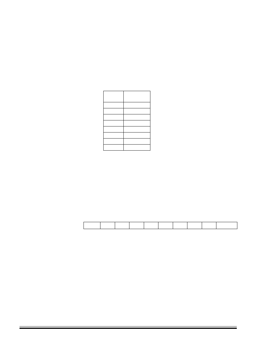
Parallel Input/Output
Port C
MC68HC11P2 -- Rev 1.0
Technical Data
MOTOROLA
Parallel Input/Output
77
4.5 Port C
Port C is an 8-bit bidirectional port, with both data and data direction
registers. In addition to their I/O capability, port C pins are used as the
nonmultiplexed data bus pins, as shown in the following table.
The state of the pins on reset is mode dependent. In single chip or
bootstrap mode, port C pins are high-impedance inputs. In expanded or
test modes, port C pins are the data bus I/O and PORTC/DDRC are not
in the memory map.
4.5.1 PORTC -- Port C data register
The bits may be read and written at any time and are not affected by
reset.
Pin
Alternate
function
PC0
D0
PC1
D1
PC2
D2
PC3
D3
PC4
D4
PC5
D5
PC6
D6
PC7
D7
In expanded or test
mode, the pins
become the data bus
and port C is not
included in the
memory map.
Address bit 7
bit 6
bit 5
bit 4
bit 3
bit 2
bit 1
bit 0
State
on reset
Port C data (PORTC)
$0006
PC7
PC6
PC5
PC4
PC3
PC2
PC1
PC0
undefined
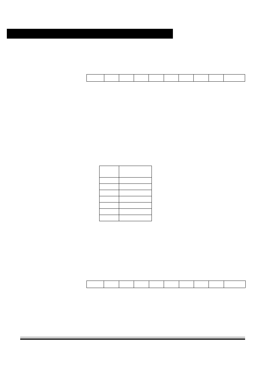
Parallel Input/Output
Technical Data
MC68HC11P2 -- Rev 1.0
78
Parallel Input/Output
MOTOROLA
4.5.2 DDRC -- Data direction register for port C
DDC[7:0] -- Data direction for port C
1 = The corresponding pin is configured as an output.
0 = The corresponding pin is configured as an input.
4.6 Port D
Port D is a 6-bit bidirectional port, with both data and data direction
registers. In addition to their I/O capability, port D pins are shared with
SCI and SPI functions, as shown in the following table.
On reset the pins are configured as general purpose high-impedance
inputs.
4.6.1 PORTD -- Port D data register
This is a read/write register and is not affected by reset. The bits may be
read and written at any time, but, when a pin is allocated to its alternate
function, a write to the corresponding register bit has no affect on the pin
state.
Address bit 7
bit 6
bit 5
bit 4
bit 3
bit 2
bit 1
bit 0
State
on reset
Data direction C (DDRC)
$0007 DDC7 DDC6 DDC5 DDC4 DDC3 DDC2 DDC1 DDC0 0000 0000
Pin
Alternate
function
PD0
RXD1
PD1
TXD1
PD2
MISO
PD3
MOSI
PD4
SCK
PD5
SS
See
Serial Peripheral
Interface (SPI)
for more
information.
See
Serial
Communications Interface
(SCI)
for more information.
Address bit 7
bit 6
bit 5
bit 4
bit 3
bit 2
bit 1
bit 0
State
on reset
Port D data (PORTD)
$0008
0
0
PD5
PD4
PD3
PD2
PD1
PD0
undefined

Parallel Input/Output
Port E
MC68HC11P2 -- Rev 1.0
Technical Data
MOTOROLA
Parallel Input/Output
79
4.6.2 DDRD -- Data direction register for port D
Bits [7:6] -- Reserved; always read zero
DDD[5:0] -- Data direction for port D
1 = The corresponding pin is configured as an output.
0 = The corresponding pin is configured as an input.
4.7 Port E
Port E is an 8-bit input-only port. In addition to their input capability, port
E pins are shared with A/D functions, as shown in the following table.
On reset the pins are configured as general purpose high-impedance
inputs.
Address bit 7
bit 6
bit 5
bit 4
bit 3
bit 2
bit 1
bit 0
State
on reset
Data direction D (DDRD)
$0009
0
0
DDD5 DDD4 DDD3 DDD2 DDD1 DDD0 0000 0000
Pin
Alternate
function
PE0
AD0
PE1
AD1
PE2
AD2
PE3
AD3
PE4
AD4
PE5
AD5
PE6
AD6
PE7
AD7
See
Analog-to-Digital
Converter
for more
information.

Parallel Input/Output
Technical Data
MC68HC11P2 -- Rev 1.0
80
Parallel Input/Output
MOTOROLA
4.7.1 PORTE -- Port E data register
This is a read-only register and is not affected by reset. The bits may be
read at any time.
NOTE:
As port E shares pins with the A/D converter, a read of the this register
may affect any conversion currently in progress, if it coincides with the
sample portion of the conversion cycle. Hence, normally port E should
not be read during the sample portion of any conversion.
4.8 Port F
Port F is an 8-bit bidirectional port, with both data and data direction
registers. In addition to their I/O capability, port F pins are used as the
non-multiplexed low order address pins, as shown in the following
table.
The state of the pins on reset is mode dependent. In single chip or
bootstrap mode, port F pins are high-impedance inputs with selectable
internal pull-up resistors (see
Internal pull-up/pull-down resistors
). In
expanded or test modes, port F pins are low order address outputs and
PORTF/DDRF are not in the memory map.
Address bit 7
bit 6
bit 5
bit 4
bit 3
bit 2
bit 1
bit 0
State
on reset
Port E data (PORTE)
$000A
PE7
PE6
PE5
PE4
PE3
PE2
PE1
PE0
undefined
Pin
Alternate
function
PF0
A0
PF1
A1
PF2
A2
PF3
A3
PF4
A4
PF5
A5
PF6
A6
PF7
A7
In expanded or test
mode, the pins become
the low order address
and port F is not included
in the memory map.

Parallel Input/Output
Port G
MC68HC11P2 -- Rev 1.0
Technical Data
MOTOROLA
Parallel Input/Output
81
4.8.1 PORTF -- Port F data register
The bits may be read and written at any time and are not affected by
reset.
4.8.2 DDRF -- Data direction register for port F
DDF[7:0] -- Data direction for port F
1 = The corresponding pin is configured as an output.
0 = The corresponding pin is configured as an input.
4.9 Port G
Port G is an 8-bit bidirectional port, with both data and data direction
registers. In addition to its I/O capability, port G pin 7 (PG7) is used as
the R/W pin in expanded and test modes.
The state of PG7 on reset is mode dependent. In single chip or bootstrap
mode, PG7 is a high-impedance input. In expanded or test modes, PG7
is the R/W output. The remaining pins (PG[6:0]) are high-impedance
inputs, with software selectable internal pull-up resistors (see
Internal
pull-up/pull-down resistors
).
Address bit 7
bit 6
bit 5
bit 4
bit 3
bit 2
bit 1
bit 0
State
on reset
Port F data (PORTF)
$0005
PF7
PF6
PF5
PF4
PF3
PF2
PF1
PF0
undefined
Address bit 7
bit 6
bit 5
bit 4
bit 3
bit 2
bit 1
bit 0
State
on reset
Data direction F (DDRF)
$0003
DDF7 DDF6 DDF5 DDF4 DDF3 DDF2 DDF1 DDF0 0000 0000
Parallel Input/Output
Technical Data
MC68HC11P2 -- Rev 1.0
82
Parallel Input/Output
MOTOROLA
4.9.1 PORTG -- Port G data register
The bits may be read and written at any time and are not affected by
reset.
4.9.2 DDRG -- Data direction register for port G
DDG[7:0] -- Data direction for port G
1 = The corresponding pin is configured as an output.
0 = The corresponding pin is configured as an input.
4.10 Port H
Port H is an 8-bit bidirectional port, with both data and data direction
registers. In addition to their I/O capability, port H pins are shared with
SCI/MI BUS and PWM functions, as shown in the following table.
On reset the pins are configured as general purpose high-impedance
inputs with selectable internal resistors. The internal resistors are pull-
Address bit 7
bit 6
bit 5
bit 4
bit 3
bit 2
bit 1
bit 0
State
on reset
Port G data (PORTG)
$007E
PG7
PG6
PG5
PG4
PG3
PG2
PG1
PG0
undefined
Address bit 7
bit 6
bit 5
bit 4
bit 3
bit 2
bit 1
bit 0
State
on reset
Data direction G (DDRG)
$007F DDG7 DDG6 DDG5 DDG4 DDG3 DDG2 DDG1 DDG0 0000 0000
Pin
Alternate
function
PH0
PW1
PH1
PW2
PH2
PW3
PH3
PW4
PH4
RXD2
PH5
TXD2
PH6
RXD3
PH7
TXD3
See
Timing System
for more information.
See
Serial Communications
Interface (SCI)
and
Motorola
Interconnect Bus (MI BUS)
for more information.

Parallel Input/Output
Internal pull-up/pull-down resistors
MC68HC11P2 -- Rev 1.0
Technical Data
MOTOROLA
Parallel Input/Output
83
ups on pins 7≠4 and pull-downs on pins 3≠0 (see
Internal pull-up/pull-
down resistors
).
4.10.1 PORTH -- Port H data register
This is a read/write register and is not affected by reset. The bits may be
read and written at any time, but, when a pin is allocated to its alternate
function, a write to the corresponding register bit has no affect on the pin
state.
4.10.2 DDRH -- Data direction register for port H
DDH[7:0] -- Data direction for port H
1 = The corresponding pin is configured as an output.
0 = The corresponding pin is configured as an input.
4.11 Internal pull-up/pull-down resistors
Three of the ports (B, F and G) have internal, software selectable pull-up
resistors. Port H has both pull-up and pull-down resistors, as described
below.
Address bit 7
bit 6
bit 5
bit 4
bit 3
bit 2
bit 1
bit 0
State
on reset
Port H data (PORTH)
$007C
PH7
PH6
PH5
PH4
PH3
PH2
PH1
PH0
undefined
Address bit 7
bit 6
bit 5
bit 4
bit 3
bit 2
bit 1
bit 0
State
on reset
Data direction H (DDRH)
$007D DDH7 DDH6 DDH5 DDH4 DDH3 DDH2 DDH1 DDH0 0000 0000

Parallel Input/Output
Technical Data
MC68HC11P2 -- Rev 1.0
84
Parallel Input/Output
MOTOROLA
4.11.1 PPAR -- Port pull-up assignment register
Bits [7:4] -- Not implemented; always read zero
xPPUE -- Port x pin pull-up enable
These bits control the on-chip pull-up devices connected to all the
pins on I/O ports B, F, G and H. They are collectively enabled or
disabled via the PAREN bit in the CONFIG register (see below).
1 = Port x pin on-chip pull-up devices enabled.
0 = Port x pin on-chip pull-up devices disabled.
NOTE:
Port H [7:4] have pull-up resistors; port H [3:0] have pull-down resistors.
All eight internal resistors are enabled if HPPUE is set.
NOTE:
FPPUE and BPPUE have no effect in expanded mode since ports F and
B are dedicated address bus outputs.
4.12 System configuration
One bit in each of the following registers is directly concerned with the
configuration of the I/O ports. For full details on the other bits in the
registers, refer to the appropriate section.
4.12.1 OPT2 -- System configuration options register 2
LIRDV -- LIR driven (refer to
Operating Modes and On-Chip Memory
)
1 = Enable LIR drive high pulse.
0 = LIR only driven low ≠ requires pull-up on pin.
Address bit 7
bit 6
bit 5
bit 4
bit 3
bit 2
bit 1
bit 0
State
on reset
Port pull-up assignment (PPAR)
$002C
0
0
0
0
HPPUEGPPUEFPPUEBPPUE 0000 1111
Address bit 7
bit 6
bit 5
bit 4
bit 3
bit 2
bit 1
bit 0
State
on reset
System config. options 2 (OPT2) $0038 LIRDV CWOMSTRCH IRVNE LSBF SPR2
0
0
000x 0000

Parallel Input/Output
System configuration
MC68HC11P2 -- Rev 1.0
Technical Data
MOTOROLA
Parallel Input/Output
85
CWOM -- Port C wired-OR mode
1 = Port C outputs are open-drain.
0 = Port C operates normally.
STRCH -- Stretch external accesses (refer to
Operating Modes and
On-Chip Memory
)
1 = Off-chip accesses are extended by one E clock cycle.
0 = Normal operation.
IRVNE -- Internal read visibility/not E (refer to
Operating Modes and
On-Chip Memory
)
1 = Data from internal reads is driven out of the external data bus.
0 = No visibility of internal reads on external bus.
In single chip mode this bit determines whether the E clock drives
out from the chip.
1 = E pin is driven low.
0 = E clock is driven out from the chip.
LSBF -- LSB first enable (refer to
Serial Peripheral Interface (SPI)
)
1 = Data is transferred LSB first.
0 = Data is transferred MSB first.
SPR2 -- SPI clock rate select (refer to
Serial Peripheral Interface
(SPI)
)
Bits 1, 0 -- not implemented; always read zero.
4.12.2 CONFIG -- System configuration register
ROMAD -- ROM mapping control (refer to
Operating Modes and On-
Chip Memory
)
1 = ROM addressed from $8000 to $FFFF.
0 = ROM addressed from $0000 to $7FFF (expanded mode only).
Bits 6,5 -- Not implemented; always read one
Address bit 7
bit 6
bit 5
bit 4
bit 3
bit 2
bit 1
bit 0
State
on reset
Configuration control (CONFIG)
$003F ROMAD
1
1
PARENNOSECNOCOPROMON EEON x11x 1xxx

Parallel Input/Output
Technical Data
MC68HC11P2 -- Rev 1.0
86
Parallel Input/Output
MOTOROLA
PAREN -- Pull-up assignment register enable
1 = PPAR register enabled; pull-ups can be enabled using PPAR.
0 = PPAR register disabled; all pull-ups disabled.
NOSEC -- EEPROM security disabled (refer to
Operating Modes and
On-Chip Memory
)
1 = Disable security.
0 = Enable security.
NOCOP -- COP system disable (refer to
Resets and Interrupts
)
1 = COP system disabled.
0 = COP system enabled (forces reset on timeout).
ROMON -- ROM enable (refer to
Operating Modes and On-Chip
Memory
)
1 = ROM present in the memory map.
0 = ROM disabled from the memory map.
EEON -- EEPROM enable (refer to
Operating Modes and On-Chip
Memory
)
1 = EEPROM is present in the memory map.
0 = EEPROM is disabled from the memory map.

MC68HC11P2 -- Rev 1.0
Technical Data
MOTOROLA
Serial Communications Interface (SCI)
87
Technical Data -- MC68HC11P2
Section 5. Serial Communications Interface (SCI)
5.1 Contents
5.2
Introduction. . . . . . . . . . . . . . . . . . . . . . . . . . . . . . . . . . . . . . . 87
5.3
Data format . . . . . . . . . . . . . . . . . . . . . . . . . . . . . . . . . . . . . . . 88
5.4
Transmit operation . . . . . . . . . . . . . . . . . . . . . . . . . . . . . . . . . 89
5.5
Receive operation. . . . . . . . . . . . . . . . . . . . . . . . . . . . . . . . . . 89
5.6
Wakeup feature . . . . . . . . . . . . . . . . . . . . . . . . . . . . . . . . . . . . 91
5.7
SCI error detection . . . . . . . . . . . . . . . . . . . . . . . . . . . . . . . . . 92
5.8
SCI registers . . . . . . . . . . . . . . . . . . . . . . . . . . . . . . . . . . . . . . 93
5.9
Status flags and interrupts . . . . . . . . . . . . . . . . . . . . . . . . . 101
5.10
Additional SCI subsystems . . . . . . . . . . . . . . . . . . . . . . . . . 104
5.2 Introduction
The serial communications interface (SCI) is a universal asynchronous
receiver transmitter (UART). It has a non-return to zero (NRZ) format
(one start, eight or nine data, and one stop bit) that is compatible with
standard RS-232 systems.
The MC68HC11P2 contains three serial communications interfaces, all
having similar operation. For ease of reference, a full description of SCI1
(PD0/RXD1, PD1/TXD1) is given first, followed by summaries for
SCI2
and
SCI3
, detailing their differences.

Serial Communications Interface (SCI)
Technical Data
MC68HC11P2 -- Rev 1.0
88
Serial Communications Interface (SCI)
MOTOROLA
The SCI shares I/O with two of port D's pins:
The SCI transmit and receive functions are enabled by TE and RE
respectively, in SCCR2.
The SCI features enabled on this MCU include: 13-bit modulus
prescaler; idle line detect; receiver-active flag; transmitter and receiver
hardware parity. A block diagram of the enhanced baud rate generator
is shown in
Figure 5-1
. See
Table 5-1
for example baud rate control
values.
5.3 Data format
The serial data format requires the following conditions:
∑
An idle-line condition before transmission or reception of a
message.
∑
A start bit, logic zero, transmitted or received, that indicates the
start of each character.
∑
Data that is transmitted and received least significant bit (LSB)
first.
Pin
Alternate
function
PD0
RXD1
PD1
TXD1
Figure 5-1. SCI baud rate generator circuit diagram
13-bit compare
Sync
SCBDH/L: SCI baud control
13-bit counter
˜
2
Internal
phase 2 clock
Receiver
baud rate
clock
˜
16
Transmitter
baud rate
clock
ST4XCK
Reset
EQ

Serial Communications Interface (SCI)
Transmit operation
MC68HC11P2 -- Rev 1.0
Technical Data
MOTOROLA
Serial Communications Interface (SCI)
89
∑
A stop bit, logic one, used to indicate the end of a frame. (A frame
consists of a start bit, a character of eight or nine data bits, and a
stop bit.)
∑
A break (defined as the transmission or reception of a logic zero
for some multiple number of frames).
Selection of the word length is controlled by the M bit of SCCR1.
5.4 Transmit operation
The SCI transmitter includes a parallel data register (SCDRH/SCDRL)
and a serial shift register. The contents of the shift register can only be
written through the serial data registers. This double buffered operation
allows a character to be shifted out serially while another character is
waiting in the serial data registers to be transferred into the shift register.
The output of the shift register is applied to TXD as long as transmission
is in progress or the transmit enable (TE) bit of serial communication
control register 2 (SCCR2) is set. The block diagram,
Figure 5-2
, shows
the transmit serial shift register and the buffer logic at the top of the
figure.
5.5 Receive operation
During receive operations, the transmit sequence is reversed. The serial
shift register receives data and transfers it to the parallel receive data
registers (SCDRH/SCDRL) as a complete word. This double buffered
operation allows a character to be shifted in serially while another
character is still in the serial data registers. An advanced data recovery
scheme distinguishes valid data from noise in the serial data stream.
The data input is selectively sampled to detect receive data, and majority
sampling logic determines the value and integrity of each bit.
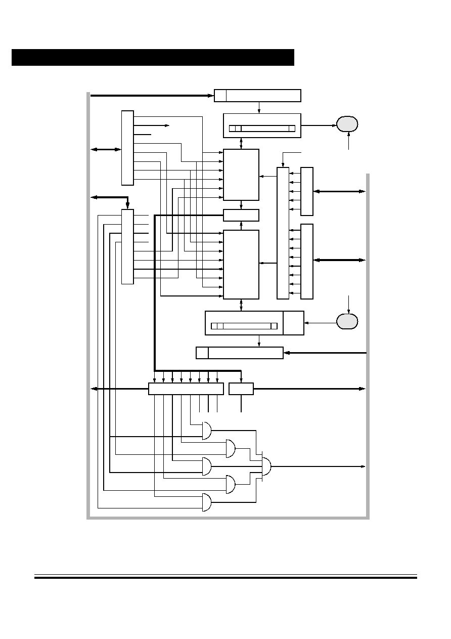
Serial Communications Interface (SCI)
Technical Data
MC68HC11P2 -- Rev 1.0
90
Serial Communications Interface (SCI)
MOTOROLA
Figure 5-2. SCI1 block diagram
LOOPS
WOMS
WAKE
+
&
&
&
&
&
M
ILT
PE
PT
SCCR
1
10/11-bit TX shift register
H 8
L
0
7
10/11-bit RX shift register
8
0
7
TIE
TCIE
TE
RIE
ILIE
RE
RWU
SBK
S
CCR2
TD
RE
TC
OR
RDR
F
ID
LE
NF
FE
PF
SCSR1
RA
F
SCSR2
Data
recovery
RXD1
TXD1
Receive buffer
R8
Transmit buffer
T8
Transmitter
control
Receiver
control
LOOPS
SCI interrupt request
WOMS
WOMS
M
PE
PT
TE
SBK
WAKE
PE
PT
RE
RWU
M
LOOPS
ILT
STOP
START
S
CBDL
S
C
BDH
R
a
te
ge
ne
rat
o
r
ST4XCK
OR
RIE
RIE
IDLE
ILIE
RDRF
TC
TCIE
TDRE
TIE
Note: = always reads as zero
Flag control
Internal data bus
clock

Serial Communications Interface (SCI)
Wakeup feature
MC68HC11P2 -- Rev 1.0
Technical Data
MOTOROLA
Serial Communications Interface (SCI)
91
5.6 Wakeup feature
The wakeup feature reduces SCI service overhead in multiple receiver
systems. Software for each receiver evaluates the first character or
frame of each message. All receivers are placed in wakeup mode by
writing a one to the RWU bit in the SCCR2 register. When RWU is set,
the receiver-related status flags (RDRF, IDLE, OR, NF, FE, and PF) are
inhibited (cannot be set). Although RWU can be cleared by a software
write to SCCR2, to do so would be unusual. Normally RWU is set by
software and is cleared automatically with hardware. Whenever a new
message begins, logic alerts the dormant receivers to wake up and
evaluate the initial character of the new message.
Two methods of wakeup are available: idle-line wakeup and address
mark wakeup. During idle-line wakeup, a dormant receiver activates as
soon as the RXD line becomes idle. In the address mark wakeup, logic
one in the most significant bit (MSB) of a character activates all sleeping
receivers. To use either receiver wakeup method, establish a software
addressing scheme to allow the transmitting devices to direct messages
to individual receivers or to groups of receivers. This addressing scheme
can take any form as long as all transmitting and receiving devices are
programmed to understand the same scheme.
5.6.1 Idle-line wakeup
Clearing the WAKE bit in SCCR1 register enables idle-line wakeup
mode. In idle-line wakeup mode, all receivers are active (RWU bit in
SCCR2 = 0) when each message begins. The first frames of each
message are addressing frames. Each receiver in the system evaluates
the addressing frames of a message to determine if the message is
intended for that receiver. When a receiver finds that the message is not
intended for it, it sets the RWU bit. Once set, the RWU control bit
disables all but the necessary receivers for the remainder of the
message, thus reducing software overhead for the remainder of that
message. As soon as an idle line is detected by receiver logic, hardware
automatically clears the RWU bit so that the first frames of the next
message can be evaluated by all receivers in the system. This type of

Serial Communications Interface (SCI)
Technical Data
MC68HC11P2 -- Rev 1.0
92
Serial Communications Interface (SCI)
MOTOROLA
receiver wakeup requires a minimum of one idle frame time between
messages, and no idle time between frames within a message.
5.6.2 Address-mark wakeup
Setting the WAKE bit in SCCR1 register enables address-mark wakeup
mode. The address-mark wakeup method uses the MSB of each frame
to differentiate between address information (MSB = 1) and actual
message data (MSB = 0). All frames consist of seven information bits
(eight bits if M bit in SCCR1 = 1) and an MSB which, when set to one,
indicates an address frame. The first frames of each message are
addressing frames. Receiver logic evaluates these marked frames to
determine the receivers for which that message is intended. When a
receiver finds that the message is not intended for it, it sets the RWU bit.
Once set, the RWU control bit disables all but the necessary receivers
for the remainder of the message, thus reducing software overhead for
the remainder of that message. When the next message begins, its first
frame will have the MSB set which will automatically clear the RWU bit
and indicate that this is an addressing frame. This frame is always the
first frame received after wakeup because the RWU bit is cleared before
the stop bit for the first frame is received. This method of wakeup allows
messages to include idle times, however, there is a loss in efficiency due
to the extra bit time required for the address bit in each frame.
5.7 SCI error detection
Four error conditions can occur during SCI operation. These error
conditions are: serial data register overrun, received bit noise, framing,
and parity error. Four bits (OR, NF, FE, and PF) in serial
communications status register 1 (SCSR1) indicate if one of these error
conditions exists.
The overrun error (OR) bit is set when the next byte is ready to be
transferred from the receive shift register to the serial data registers
(SCDRH/SCDRL) and the registers are already full (RDRF bit is set).
When an overrun error occurs, the data that caused the overrun is lost
and the data that was already in serial data registers is not disturbed.

Serial Communications Interface (SCI)
SCI registers
MC68HC11P2 -- Rev 1.0
Technical Data
MOTOROLA
Serial Communications Interface (SCI)
93
The OR is cleared when the SCSR is read (with OR set), followed by a
read of the SCI data registers.
The noise flag (NF) bit is set if there is noise on any of the received bits,
including the start and stop bits. The NF bit is not set until the RDRF flag
is set. The NF bit is cleared when the SCSR is read (with FE equal to
one) followed by a read of the SCI data registers.
When no stop bit is detected in the received data character, the framing
error (FE) bit is set. FE is set at the same time as the RDRF. If the byte
received causes both framing and overrun errors, the processor only
recognizes the overrun error. The framing error flag inhibits further
transfer of data into the SCI data registers until it is cleared. The FE bit
is cleared when the SCSR is read (with FE equal to one) followed by a
read of the SCI data registers.
The parity error flag (PF) is set if received data has incorrect parity. The
flag is cleared by a read of SCSR1 with PE set, followed by a read of
SCDR.
5.8 SCI registers
There are eight addressable registers in the SCI. SCBDH, SCBDL,
SCCR1, and SCCR2 are control registers. The contents of these
registers control functions and indicate conditions within the SCI. The
status registers SCSR1 and SCSR2 contain bits that indicate certain
conditions within the SCI. SCDRH and SCDRL are SCI data registers.
These double buffered registers are used for the transmission and
reception of data, and are used to form the 9-bit data word for the SCI.
If the SCI is being used with 7 or 8-bit data, only SCDRL needs to be
accessed. Note that if 9-bit data format is used, the upper register should
be written first to ensure that it is transferred to the transmitter shift
register with the lower register.

Serial Communications Interface (SCI)
Technical Data
MC68HC11P2 -- Rev 1.0
94
Serial Communications Interface (SCI)
MOTOROLA
5.8.1 SCBDH, SCBDL -- SCI baud rate control registers
The contents of this register determine the baud rate of the SCI.
BTST -- Baud register test (Test mode only)
BSPL -- Baud rate counter split (Test mode only)
Bit 5 -- Not implemented; always reads zero
SBR[12:0] -- SCI baud rate selects
Use the following formula to calculate SCI baud rate. Refer to the
table of baud rate control values for example rates:
where the baud rate control value (BR) is the contents of SCBDH/L
(BR = 1, 2, 3,... 8191).
BR = 0 disables the baud rate generator. For example, to obtain a
baud rate of 1200 with a 12MHz crystal, the baud register (SCBDH/L)
should contain $0138 (see
Table 5-1
).
NOTE:
ST4XCK may be the output of the PLL circuit or it may be the EXTAL
input of the MCU. Selection is made by the MCS bit in the PLLCR (see
Crystal driver and external clock input (XTAL, EXTAL)
).
Address bit 7
bit 6
bit 5
bit 4
bit 3
bit 2
bit 1
bit 0
State
on reset
SCI 1 baud rate high (SCBDH)
$0070
BTST BSPL
0
SBR12 SBR11 SBR10 SBR9 SBR8 0000 0000
SCI 1 baud rate low (SCBDL)
$0071
SBR7 SBR6 SBR5 SBR4 SBR3 SBR2 SBR1 SBR0 0000 0100
SCI baud rate
ST
4
XCK
16
2
BR
(
)
◊
-----------------------------
=

Serial Communications Interface (SCI)
SCI registers
MC68HC11P2 -- Rev 1.0
Technical Data
MOTOROLA
Serial Communications Interface (SCI)
95
5.8.2 SCCR1 -- SCI control register 1
The SCCR1 register provides the control bits that determine word length
and select the method used for the wakeup feature.
LOOPS -- SCI loop mode enable
1 = SCI transmit and receive are disconnected from TXD and RXD
pins, and transmitter output is fed back into the receiver input.
0 = SCI transmit and receive operate normally.
Both the transmitter and receiver must be enabled to use the LOOP
mode. When the LOOP mode is enabled, the TXD pin is driven high
(idle line state) if the transmitter is enabled.
WOMS -- Wired-OR mode for SCI pins (PD1, PD0)
1 = TXD and RXD are open drains if operating as outputs.
0 = TXD and RXD operate normally.
Bit 5 -- Not implemented; always reads zero
Table 5-1. Example SCI baud rate control values
Target
baud
rate
Crystal frequency (EXTAL)
8 MHz
12 MHz
16 MHz
Dec
value
Hex
value
Dec
value
Hex
value
Dec
value
Hex
value
110
2272
$08E0
3409
$0D51
4545
$11C1
150
1666
$0682
2500
$09C4
3333
$0D05
300
833
$0341
1250
$04E2
1666
$0682
600
416
$01A0
625
$0271
833
$0341
1 200
208
$00D0
312
$0138
416
$01A0
2 400
104
$0068
156
$009C
208
$00D0
4 800
52
$0034
78
$004E
104
$0068
9 600
26
$001A
39
$0027
52
$0034
19 200
13
$000D
20
$0014
26
$001A
38 400
13
$000D
Address bit 7
bit 6
bit 5
bit 4
bit 3
bit 2
bit 1
bit 0
State
on reset
SCI 1 control 1 (SCCR1)
$0072
LOOP
S
WOMS
0
M
WAKE
ILT
PE
PT
0000 0000

Serial Communications Interface (SCI)
Technical Data
MC68HC11P2 -- Rev 1.0
96
Serial Communications Interface (SCI)
MOTOROLA
M -- Mode (select character format)
1 = Start bit, 9 data bits, 1 stop bit.
0 = Start bit, 8 data bits, 1 stop bit.
WAKE -- Wakeup by address mark/idle
1 = Wakeup by address mark (most significant data bit set).
0 = Wakeup by IDLE line recognition.
ILT -- Idle line type
1 = Long (SCI counts ones only after stop bit).
0 = Short (SCI counts consecutive ones after start bit).
This bit determines which of two types of idle line detection method is
used by the SCI receiver. In short mode the stop bit and any bits that
were ones before the stop bit will be considered as part of that string
of ones, possibly resulting in erroneous or premature detection of an
idle line condition. In long mode the SCI system does not begin
counting ones until a stop bit is received.
PE -- Parity enable
1 = Parity enabled.
0 = Parity disabled.
PT -- Parity type
1 = Parity odd (an odd number of ones causes parity bit to be zero,
an even number of ones causes parity bit to be one).
0 = Parity even (an even number of ones causes parity bit to be
zero, an odd number of ones causes parity bit to be one).

Serial Communications Interface (SCI)
SCI registers
MC68HC11P2 -- Rev 1.0
Technical Data
MOTOROLA
Serial Communications Interface (SCI)
97
5.8.3 SCCR2 -- SCI control register 2
The SCCR2 register provides the control bits that enable or disable
individual SCI functions.
TIE -- Transmit interrupt enable
1 = SCI interrupt requested when TDRE status flag is set.
0 = TDRE interrupts disabled.
TCIE -- Transmit complete interrupt enable
1 = SCI interrupt requested when TC status flag is set.
0 = TC interrupts disabled.
RIE -- Receiver interrupt enable
1 = SCI interrupt requested when RDRF flag or the OR status flag
is set.
0 = RDRF and OR interrupts disabled.
ILIE -- Idle line interrupt enable
1 = SCI interrupt requested when IDLE status flag is set.
0 = IDLE interrupts disabled.
TE -- Transmitter enable
1 = Transmitter enabled.
0 = Transmitter disabled.
RE -- Receiver enable
1 = Receiver enabled.
0 = Receiver disabled.
RWU -- Receiver wakeup control
1 = Wakeup enabled and receiver interrupts inhibited.
0 = Normal SCI receiver.
SBK -- Send break
1 = Break codes generated as long as SBK is set.
0 = Break generator off.
Address bit 7
bit 6
bit 5
bit 4
bit 3
bit 2
bit 1
bit 0
State
on reset
SCI 1 control 2 (SCCR2)
$0073
TIE
TCIE
RIE
ILIE
TE
RE
RWU
SBK 0000 0000

Serial Communications Interface (SCI)
Technical Data
MC68HC11P2 -- Rev 1.0
98
Serial Communications Interface (SCI)
MOTOROLA
5.8.4 SCSR1 -- SCI status register 1
The bits in SCSR1 indicate certain conditions in the SCI hardware and
are automatically cleared by special acknowledge sequences.
TDRE -- Transmit data register empty flag
1 = SCDR empty.
0 = SCDR busy.
This flag is set when SCDR is empty. Clear the TDRE flag by reading
SCSR1 with TDRE set and then writing to SCDR.
TC -- Transmit complete flag
1 = Transmitter idle.
0 = Transmitter busy.
This flag is set when the transmitter is idle (no data, preamble, or
break transmission in progress). Clear the TC flag by reading SCSR1
with TC set and then writing to SCDR.
RDRF -- Receive data register full flag
1 = SCDR full.
0 = SCDR empty.
Once cleared, IDLE is not set again until the RXD line has been active
and becomes idle again. RDRF is set if a received character is ready
to be read from SCDR. Clear the RDRF flag by reading SCSR1 with
RDRF set and then reading SCDR.
IDLE -- Idle line detected flag
1 = RXD line is idle.
0 = RXD line is active.
This flag is set if the RXD line is idle. Once cleared, IDLE is not set
again until the RXD line has been active and becomes idle again. The
IDLE flag is inhibited when RWU = 1. Clear IDLE by reading SCSR1
with IDLE set and then reading SCDR.
Address bit 7
bit 6
bit 5
bit 4
bit 3
bit 2
bit 1
bit 0
State
on reset
SCI 1 status 1 (SCSR1)
$0074 TDRE
TC
RDRF IDLE
OR
NF
FE
PF
1100 0000

Serial Communications Interface (SCI)
SCI registers
MC68HC11P2 -- Rev 1.0
Technical Data
MOTOROLA
Serial Communications Interface (SCI)
99
OR -- Overrun error flag
1 = Overrun detected.
0 = No overrun.
OR is set if a new character is received before a previously received
character is read from SCDR. Clear the OR flag by reading SCSR1
with OR set and then reading SCDR.
NF -- Noise error flag
1 = Noise detected.
0 = Unanimous decision.
NF is set if the majority sample logic detects anything other than a
unanimous decision. Clear NF by reading SCSR1 with NF set and
then reading SCDR.
FE -- Framing error
1 = Zero detected.
0 = Stop bit detected.
FE is set when a zero is detected where a stop bit was expected.
Clear the FE flag by reading SCSR1 with FE set and then reading
SCDR.
PF -- Parity error flag
1 = Incorrect parity detected.
0 = Parity correct.
PF is set if received data has incorrect parity. Clear PF by reading
SCSR1 with PE set and then reading SCDR.

Serial Communications Interface (SCI)
Technical Data
MC68HC11P2 -- Rev 1.0
100
Serial Communications Interface (SCI)
MOTOROLA
5.8.5 SCSR2 -- SCI status register 2
In the SCSR2 only bit 0 is used, to indicate receiver active. The other
seven bits always read zero.
Bits [7:1] -- Not implemented; always read zero
RAF -- Receiver active flag (read only)
1 = A character is being received.
0 = A character is not being received.
5.8.6 SCDRH, SCDRL -- SCI data high/low registers
SCDRH/SCDRL is a parallel register that performs two functions. It is the
receive data register when it is read, and the transmit data register when
it is written. Reads access the receive data buffer and writes access the
transmit data buffer. Data received or transmitted is double buffered.
R8 -- Receiver bit 8
Ninth serial data bit received when SCI is configured for a nine data
bit operation
T8 -- Transmitter bit 8
Ninth serial data bit transmitted when SCI is configured for a nine data
bit operation
Bits [5:0] -- Not implemented; always read zero
R/T[7:0] -- Receiver/transmitter data bits [7:0]
SCI data is double buffered in both directions.
Address bit 7
bit 6
bit 5
bit 4
bit 3
bit 2
bit 1
bit 0
State
on reset
SCI 1 status 2 (SCSR2)
$0075
0
0
0
0
0
0
0
RAF 0000 0000
Address bit 7
bit 6
bit 5
bit 4
bit 3
bit 2
bit 1
bit 0
State
on reset
SCI 1 data high (SCDRH)
$0076
R8
T8
0
0
0
0
0
0
undefined
SCI 1 data low (SCDRL)
$0077
R7T7 R6T6
R5T5
R4T4 R3T3
R2T2
R1T1
R0T0 undefined

Serial Communications Interface (SCI)
Status flags and interrupts
MC68HC11P2 -- Rev 1.0
Technical Data
MOTOROLA
Serial Communications Interface (SCI)
101
5.9 Status flags and interrupts
The SCI transmitter has two status flags. These status flags can be read
by software (polled) to tell when certain conditions exist. Alternatively, a
local interrupt enable bit can be set to enable each of these status
conditions to generate interrupt requests. Status flags are automatically
set by hardware logic conditions, but must be cleared by software. This
provides an interlock mechanism that enables logic to know when
software has noticed the status indication. The software clearing
sequence for these flags is automatic -- functions that are normally
performed in response to the status flags also satisfy the conditions of
the clearing sequence.
TDRE and TC flags are normally set when the transmitter is first enabled
(TE set to one). The TDRE flag indicates there is room in the transmit
queue to store another data character in the transmit data register. The
TIE bit is the local interrupt mask for TDRE. When TIE is zero, TDRE
must be polled. When TIE and TDRE are one, an interrupt is requested.
The TC flag indicates the transmitter has completed the queue. The
TCIE bit is the local interrupt mask for TC. When TCIE is zero, TC must
be polled; when TCIE is one and TC is one, an interrupt is requested.
Writing a zero to TE requests that the transmitter stop when it can. The
transmitter completes any transmission in progress before shutting
down. Only an MCU reset can cause the transmitter to stop and shut
down immediately. If TE is cleared when the transmitter is already idle,
the pin reverts to its general-purpose I/O function (synchronized to the
bit-rate clock). If anything is being transmitted when TE is cleared, that
character is completed before the pin reverts to general-purpose I/O, but
any other characters waiting in the transmit queue are lost. The TC and
TDRE flags are set at the completion of this last character, even though
TE has been disabled.

Serial Communications Interface (SCI)
Technical Data
MC68HC11P2 -- Rev 1.0
102
Serial Communications Interface (SCI)
MOTOROLA
5.9.1 Receiver flags
The SCI receiver has seven status flags, three of which can generate
interrupt requests. The status flags are set by the SCI logic in response
to specific conditions in the receiver. These flags can be read (polled) at
any time by software. Refer to
Figure 5-3
, which shows SCI interrupt
arbitration.
When an overrun takes place, the new character is lost, and the
character that was in its way in the parallel receive data register (RDR)
is undisturbed. RDRF is set when a character has been received and
transferred into the parallel RDR. The OR flag is set instead of RDRF if
overrun occurs. A new character is ready to be transferred into the RDR
before a previous character is read from the RDR.
The NF, FE and PF flags provide additional information about the
character in the RDR, but do not generate interrupt requests.
The receiver active flag (RAF) indicates that the receiver is busy.
The last receiver status flag and interrupt source come from the IDLE
flag. The RXD line is idle if it has constantly been at logic one for a full
character time. The IDLE flag is set only after the RXD line has been
busy and becomes idle. This prevents repeated interrupts for the time
RXD remains idle.
Serial Communications Interface (SCI)
Status flags and interrupts
MC68HC11P2 -- Rev 1.0
Technical Data
MOTOROLA
Serial Communications Interface (SCI)
103
Figure 5-3. Interrupt source resolution within SCI
No
Begin
RDRF = 1?
OR = 1?
TDRE = 1?
TC = 1?
IDLE = 1?
No valid SCI
interrupt request
RIE = 1?
TE = 1?
RE = 1?
TIE = 1?
TCIE = 1?
ILIE = 1?
RE = 1?
Valid SCI
interrupt request
Yes
Yes
Yes
Yes
Yes
Yes
Yes
Yes
Yes
Yes
Yes
Yes
No
No
No
No
No
No
No
No
No
No
No
Note: The bit names shown are for SCI1. The
diagram applies equally to SCI2 and SCI3,
when the appropriate bit names are
substituted.
Serial Communications Interface (SCI)
Technical Data
MC68HC11P2 -- Rev 1.0
104
Serial Communications Interface (SCI)
MOTOROLA
5.10 Additional SCI subsystems
In addition to the subsystem described in the above paragraphs (SCI1),
the MC68HC11P2 has two other, similar, SCI modules (SCI2, SCI3).
These two systems are identical to that described, with the following
exceptions:
SCI2 and SCI3 share I/O with four port H pins:
The SCI2 transmit and receive functions are enabled by TE2 and RE2
respectively, in S2CR2; similarly, the SCI3 transmit and receive
functions are enabled by TE3 and RE3 respectively, in S3CR2.
SCI1 functions and data are handled by a register block at
$0070≠$0077. The corresponding registers for SCI2 and SCI3 are at
addresses $0050≠$0057 and $005A≠$005F respectively, as shown in
the following sections.
SCI2 and SCI3 share the same baud rate register (at $0050/51).
In addition to their SCI functions, these two subsystems are also used
for MI BUS, controlled by bit 5 of their respective SCCR1 registers. Refer
to
Motorola Interconnect Bus (MI BUS)
for full details of MI BUS
operation.
5.10.1 SCI2
SCI2 shares I/O with two of port H's pins: receive pin RXD2/PH6 and
transmit pin TXD2/PD7. The SCI receive and transmit functions are
enabled by RE and TE respectively, in S2CR2.
Pin
Alternate
function
PH4
RXD2
PH5
TXD2
PH6
RXD3
PH7
TXD3

Serial Communications Interface (SCI)
Additional SCI subsystems
MC68HC11P2 -- Rev 1.0
Technical Data
MOTOROLA
Serial Communications Interface (SCI)
105
5.10.1.1 S2BDH, S2BDL -- SCI2/3 baud rate control registers
The contents of this register determine the baud rate for both SCI2 and
SCI3. For details of the bits and the corresponding baud rates see
SCBDH, SCBDL -- SCI baud rate control registers
. This register also
controls the MI BUS clock rate (see
Motorola Interconnect Bus
(MI BUS)
).
5.10.1.2 S2CR1 -- SCI2 control register 1
The S2CR1 register provides the control bits that determine word length
and select the method used for the wakeup feature. Bit 5 has an MI BUS
control function detailed below (for details of the other bits see
SCCR1
-- SCI control register 1
).
MIE2 -- Motorola interface bus enable 2
1 = MI BUS is enabled for this subsystem.
0 = The SCI functions normally.
When MIE2 is set, the SCI2 registers, bits and pins assume the
functionality required for MI BUS.
5.10.1.3 S2CR2 -- SCI2 control register 2
The S2CR2 register provides the control bits that enable or disable
individual SCI functions. For details of the bits, see
SCCR2 -- SCI
control register 2
.
Address bit 7
bit 6
bit 5
bit 4
bit 3
bit 2
bit 1
bit 0
State
on reset
SCI/MI 2/3 baud high (S2BDH)
$0050 B2TST B2SPL
0
S2B12 S2B11 S2B10 S2B9
S2B8 0000 0000
SCI/MI 2/3 baud low (S2BDL)
$0051
S2B7
S2B6
S2B5
S2B4
S2B3
S2B2
S2B1
S2B0 0000 0100
Address bit 7
bit 6
bit 5
bit 4
bit 3
bit 2
bit 1
bit 0
State
on reset
SCI/MI 2 control 1 (S2CR1)
$0052 LOPS2
WOMS
2
MIE2
M2
WAKE
2
ILT2
PE2
PT2 0000 0000
Address bit 7
bit 6
bit 5
bit 4
bit 3
bit 2
bit 1
bit 0
State
on reset
SCI/MI 2 control 2 (S2CR2)
$0053
TIE2 TCIE2 RIE2
ILIE2
TE2
RE2
RWU2 SBK2 0000 0000

Serial Communications Interface (SCI)
Technical Data
MC68HC11P2 -- Rev 1.0
106
Serial Communications Interface (SCI)
MOTOROLA
5.10.1.4 S2SR1 -- SCI2 status register 1
The bits in S2SR1 indicate certain conditions in the SCI hardware and
are automatically cleared by special acknowledge sequences. For
details of the bits, see
SCSR1 -- SCI status register 1
.
5.10.1.5 S2SR2 -- SCI2 status register 2
In the S2SR2 only bit 0 is used, to indicate receiver active (see
SCSR2
-- SCI status register 2
). The other seven bits always read zero.
5.10.1.6 S2DRH, S2DRL -- SCI2 data high/low registers
S2DRH/S2DRL is a parallel register that performs two functions. It is the
receive data register when it is read, and the transmit data register when
it is written. Reads access the receive data buffer and writes access the
transmit data buffer. Data received or transmitted is double buffered.
See
SCDRH, SCDRL -- SCI data high/low registers
for more details.
5.10.2 SCI3
SCI3 shares I/O with two of port H's pins: receive pin RXD3/PH4 and
transmit pin TXD3/PD5. The SCI receive and transmit functions are
enabled by RE and TE respectively, in S3CR2.
The baud rate of this subsystem is controlled by the baud rate register
for SCI2, hence the two SCIs always have the same baud rate.
Address bit 7
bit 6
bit 5
bit 4
bit 3
bit 2
bit 1
bit 0
State
on reset
SCI/MI 2 status 1 (S2SR1)
$0054 TDRE2 TC2 RDRF2 IDLE2
OR2
NF2
FE2
PF2 1100 0000
Address bit 7
bit 6
bit 5
bit 4
bit 3
bit 2
bit 1
bit 0
State
on reset
SCI/MI 2 status 2 (S2SR2)
$0055
0
0
0
0
0
0
0
RAF2 0000 0000
Address bit 7
bit 6
bit 5
bit 4
bit 3
bit 2
bit 1
bit 0
State
on reset
SCI/MI 2 data high (S2DRH)
$0056
R8B
T8B
0
0
0
0
0
0
undefined
SCI/MI 2 data low (S2DRL)
$0057 R7T7B R6T6B R5T5B R4T4B R3T3B R2T2B R1T1B R0T0B undefined

Serial Communications Interface (SCI)
Additional SCI subsystems
MC68HC11P2 -- Rev 1.0
Technical Data
MOTOROLA
Serial Communications Interface (SCI)
107
5.10.2.1 S3CR1 -- SCI3 control register 1
The S3CR1 register provides the control bits that determine word length
and select the method used for the wakeup feature. Bit 5 has an MI BUS
control function detailed below (for details of the other bits see
SCCR1
-- SCI control register 1
).
MIE3 -- Motorola Interface Bus Enable 3
1 = MI BUS is enabled for this subsystem.
0 = The SCI functions normally.
When MIE3 is set, the SCI3 registers, bits and pins assume the
functionality required for MI BUS.
5.10.2.2 S3CR2 -- SCI3 control register 2
The S3CR2 register provides the control bits that enable or disable
individual SCI functions. For details of the bits, see
SCCR2 -- SCI
control register 2
.
5.10.2.3 S3SR1 -- SCI3 status register 1
The bits in S3SR1 indicate certain conditions in the SCI hardware and
are automatically cleared by special acknowledge sequences. For
details of the bits, see
SCSR1 -- SCI status register 1
.
Address bit 7
bit 6
bit 5
bit 4
bit 3
bit 2
bit 1
bit 0
State
on reset
SCI/MI 3 control 1 (S3CR1)
$005A LOPS3 WOMS3 MIE3
M3
WAKE3 ILT3
PE3
PT3 0000 0000
Address bit 7
bit 6
bit 5
bit 4
bit 3
bit 2
bit 1
bit 0
State
on reset
SCI/MI 3 control 2 (S3CR2)
$005B
TIE3 TCIE3 RIE3
ILIE3
TE3
RE3
RWU3 SBK3 0000 0000
Address bit 7
bit 6
bit 5
bit 4
bit 3
bit 2
bit 1
bit 0
State
on reset
SCI/MI 3 status 1 (S3SR1)
$005C TDRE3 TC3 RDRF3 IDLE3
OR3
NF3
FE3
PF3 1100 0000

Serial Communications Interface (SCI)
Technical Data
MC68HC11P2 -- Rev 1.0
108
Serial Communications Interface (SCI)
MOTOROLA
5.10.2.4 S3SR2 -- SCI3 status register 2
In S3SR2 only bit 0 is used, to indicate receiver active (see
SCSR2 --
SCI status register 2
for details). The other seven bits always read zero.
5.10.2.5 S3DRH, S3DRL -- SCI3 data high/low registers
S3DRH/S3DRL is a parallel register that performs two functions. It is the
receive data register when it is read, and the transmit data register when
it is written. Reads access the receive data buffer and writes access the
transmit data buffer. Data received or transmitted is double buffered.
See
SCDRH, SCDRL -- SCI data high/low registers
for more details.
Address bit 7
bit 6
bit 5
bit 4
bit 3
bit 2
bit 1
bit 0
State
on reset
SCI/MI 3 status 2 (S3SR2)
$005D
0
0
0
0
0
0
0
RAF3 0000 0000
Address bit 7
bit 6
bit 5
bit 4
bit 3
bit 2
bit 1
bit 0
State
on reset
SCI/MI 3 data high (S3DRH)
$005E
R8C
T8C
0
0
0
0
0
0
undefined
SCI/MI 3 data low (S3DRL)
$005F R7T7C R6T6C R5T5C R4T4C R3T3C R2T2C R1T1C R0T0C undefined

MC68HC11P2 -- Rev 1.0
Technical Data
MOTOROLA
Motorola Interconnect Bus (MI BUS)
109
Technical Data -- MC68HC11P2
Section 6. Motorola Interconnect Bus (MI BUS)
6.1 Contents
6.2
Introduction. . . . . . . . . . . . . . . . . . . . . . . . . . . . . . . . . . . . . . 109
6.3
Push-pull sequence . . . . . . . . . . . . . . . . . . . . . . . . . . . . . . . 111
6.4
The push field . . . . . . . . . . . . . . . . . . . . . . . . . . . . . . . . . . . .112
6.5
The pull field . . . . . . . . . . . . . . . . . . . . . . . . . . . . . . . . . . . . . 112
6.6
Biphase coding . . . . . . . . . . . . . . . . . . . . . . . . . . . . . . . . . . . 113
6.7
Message validation. . . . . . . . . . . . . . . . . . . . . . . . . . . . . . . . 113
6.8
Interfacing to MI BUS . . . . . . . . . . . . . . . . . . . . . . . . . . . . . . 116
6.9
MI BUS clock rate . . . . . . . . . . . . . . . . . . . . . . . . . . . . . . . . . 117
6.10
SCI/MI BUS2 registers . . . . . . . . . . . . . . . . . . . . . . . . . . . . . 117
6.11
SCI/MI BUS3 registers . . . . . . . . . . . . . . . . . . . . . . . . . . . . . 123
6.2 Introduction
The Motorola Interconnect Bus (MI BUS) is a serial communications
protocol which supports distributed real-time control efficiently and with
a high degree of noise immunity, at a typical bit rate for the data transfer
of 20kHz. The MI BUS is suitable for medium speed networks requiring
very low cost multiplex wiring; only one wire is required to connect to
slave devices.
(1)
1. Related information on Motorola's MI BUS is contained in the following Motorola publications:
EB409/D -- The MI BUS and Product family for Multiplexing Systems
AN475/D -- Single Wire MI BUS Controlling Stepper Motors
BR477/D -- Smart Mover ≠ Stepper Motors with Integrated Serial Bus Controller

Motorola Interconnect Bus (MI BUS)
Technical Data
MC68HC11P2 -- Rev 1.0
110
Motorola Interconnect Bus (MI BUS)
MOTOROLA
The MC68HC11P2 contains two similar MI BUS modules. For ease of
reference, a full description of MI BUS2 is given, followed by a summary
of MI BUS3, detailing its differences.
The MI BUS uses a push-pull sequence to transfer data. The master
device, which, in this case, is the MC68HC11P2, sends a push field to
the slave devices connected to the bus. The push field contains data
plus an address that is recognized by one of the slaves. The slave
addressed returns data which the master pulls from the MI BUS over the
same wire. Specific details of the message format are covered later in
this section. The MCU (master) can take the bus at any time, with a start
bit that violates the rules of Manchester biphase encoding. Up to eight
slave devices may be addressed by the MI BUS. Other features of
MI BUS include message validation, error detection, and default value
setting.
On the MC68HC11P2 the MI BUS module shares the same pins on port
H as the SCI2 and SCI3 modules. Data is transmitted (or `pushed') via
the TXD pin, and received (`pulled') via the RXD pin. While data is being
pushed RXD will be disconnected from the receiver circuitry. The
message frame is handled automatically in hardware. The MCU register
interface is similar to that for the SCI.
MI BUS2 functions are enabled by MIE2 in S2CR1; MI BUS3 functions
by MIE3 in S3CR1.
Pin
Alternate
function
PH4
RXD2
PH5
TXD2
PH6
RXD3
PH7
TXD3

Motorola Interconnect Bus (MI BUS)
Push-pull sequence
MC68HC11P2 -- Rev 1.0
Technical Data
MOTOROLA
Motorola Interconnect Bus (MI BUS)
111
6.3 Push-pull sequence
Communication between the MCU and the slave device always utilizes
the same frame organization. First, the MCU sends serial data to the
selected device. This data field is called the `push field'. At the end of the
push field, the selected device automatically sends back to the MCU the
data held during the push sequence. The MCU reads the serial data sent
by the selected device. This data is called the `pull field' and contains
status information followed by the end-of-frame information from the
selected device.
Figure 6-1. MI BUS timing
1 0
0 1
1
0
2 3 4
6 7
5
Start
Stop
Start
Push
sync D0
D1
D2
D3
D4
A0
A1
A2
Pull
sync
S3
S2
S1
Data
Address
NRZ
Data
End of frame
Push field
(driven by MCU)
Pull field
(driven by slave)
Message frame
Push (biphase coded)
Pull (NRZ coded)
Ne
w
fr
am
e
Push-pull function
Time slots
TXD pin (true data)
MI BUS wire
Bit fields

Motorola Interconnect Bus (MI BUS)
Technical Data
MC68HC11P2 -- Rev 1.0
112
Motorola Interconnect Bus (MI BUS)
MOTOROLA
6.4 The push field
The push field consists of a start bit, a push synchronization bit, a push
data field and a push address field. The start consists of three time slots
having the dominant logical state `0'. The start marks the beginning of
the message frame by violation of the rule of the Manchester code. The
push synchronization bit consists of a biphase coded `0'. Biphase coding
will be discussed later. The push data field consists of five bits of biphase
coded data. The push address consists of three bits of biphase coded
data. Data and address are written to the lower byte of the SCI data
register (S2DRL). The push data occupies the lower five bits and the
push address occupies the upper three bits of the register.
6.5 The pull field
The pull field consists of a pull synchronization bit, a pull data field and
an end of frame. The pull synchronization bit is a biphase coded `1' and
is initiated by the MCU during the time slot after the last address bit of
the push field. The pull data field consists of an NRZ coded transmission,
each bit taking one time slot. Once shifted in, the pull data is stored in
the lower byte of the SCI data register (S2DRL). The end-of-frame field
is a square wave signal having a typical frequency of 20kHz ± 1%
tolerance (i.e. the bit rate of the push field) when the data sent to the
selected device is valid.
Motorola Interconnect Bus (MI BUS)
Biphase coding
MC68HC11P2 -- Rev 1.0
Technical Data
MOTOROLA
Motorola Interconnect Bus (MI BUS)
113
6.6 Biphase coding
Manchester biphase L coding is used for the push field bits. Each bit
requires two time slots to encode the logic value of the bit. This encoding
allows the detection of a single error at the time slot level. Bits are
encoded as follows:
1 = In the first time slot, the logic level is set to zero, followed by a
logic level one in the second time slot;
0 = In the first time slot, the logic level is set to one, followed by a
logic level zero in the second time slot.
6.7 Message validation
The communication between the MCU and the selected device is valid
when the MCU reads a pull data field having correct codes (excluding
the codes `111' and `000') followed by a square wave signal, having a
frequency of 20kHz, contained in the end-of-frame information.
An MI BUS error is detected when the pull field contains the code `111'
followed by the end-of-frame permanently tied to logical state `1'. This
means that the communication between the MCU and the selected
device was not accomplished.
Figure 6-2. Biphase coding and error detection
`0'
`1'
0
1
2
3
4
5
6
7
0
1
2
3
4
5
6
7
t
Biphase coded signal
Biphase detection
Noise detection
a
b
a
b
a'
b'
a
b
a'
b'
a
b

Motorola Interconnect Bus (MI BUS)
Technical Data
MC68HC11P2 -- Rev 1.0
114
Motorola Interconnect Bus (MI BUS)
MOTOROLA
6.7.1 Controller detected errors
There are three different MI BUS error types which are detected by the
selected slave device and are not mutually exclusive. The MCU cannot
determine which error occurred.
Noise error Slave devices take two samples in each time slot of
the biphase encoded push field. An error occurs when the two
samples for each time slot are not the same logical level.
Biphase error Slave devices receiving the push field detect the
biphase code. An error occurs when the two time slots of the
biphase code do not yield a logical exclusive-OR function.
Field error A field error is detected when the fixed-form of the
push field is violated.
6.7.2 MCU detected errors
There is a fourth error that can be detected by the MCU. This error
causes the noise flag (NF) to be asserted in the S2SR1 (or S3SR1)
register during the push field sequence.
Bit error A bit error can be detected by the MCU during the push
field. The MI BUS serial system monitors the bus via on-chip
hardware at the RXD pin at the same time as sending data. A bit
error is detected at that bit time when the value monitored is
different from the bit value sent.

Motorola Interconnect Bus (MI BUS)
Message validation
MC68HC11P2 -- Rev 1.0
Technical Data
MOTOROLA
Motorola Interconnect Bus (MI BUS)
115
Figure 6-3. MI BUS block diagram
LOPS2
WOMS2
WAKE2
+
&
&
&
&
&
M2
ILT2
PE2
PT2
S
2
CR1
10/11-bit TX shift register
H 8
L
0
7
10/11-bit RX shift register
8
0
7
TIE2
TE2
RIE2
ILIE2
RE2
RWU2
SBK2
S
2
CR2
T
DRE
2
TC
2
OR
2
R
DRF
2
S2SR1
RAF
2
S2SR2
Data
recovery
RXD2
TXD2
Receive buffer
R8
Transmit buffer
T8
Transmitter
control
Receiver
control
SCI interrupt request
WOMS
WOMS
MIE2
PT2
TE2
SBK2
MIE2
RE2
STOP
START
S
2
BDL
S2BDH
R
a
te gene
rator
ST4XCK
OR2
RIE2
RIE2
IDLE2
ILIE2
RDRF2
TC2
TCIE2
TDRE2
TIE2
Note: = always reads as zero
Flag control
Internal data bus
MIE2
TCIE2
NF
2
= not used in MI BUS mode
clock

Motorola Interconnect Bus (MI BUS)
Technical Data
MC68HC11P2 -- Rev 1.0
116
Motorola Interconnect Bus (MI BUS)
MOTOROLA
6.8 Interfacing to MI BUS
Physically the MI BUS consists of only a single wire. In the example
shown in
Figure 6-4
, only a single transistor and a few passive
components are required to connect up the MC68HC11P2 for full
MI BUS operation.
The transistor serves both to drive the MI BUS during the push field and
to protect the MCU TX pin from voltage transients generated in the
wiring. Without the transistor, EMI could damage the TX pin. Similarly,
the input pin (RX) is protected from EMI by clamping it to the MCU supply
rails with two diodes. When a load dump occurs, the zener diode (18V)
is switched on and hence turns the transistor on; this generates the logic
`0' state on the MI BUS. After eight time slots (200ms) of continuous `0'
state, all devices on the MI BUS will have their outputs disabled.
Figure 6-4. A typical interface between the MC68HC11P2 and the MI BUS
1.2kæ
+12V
18V
4.7kæ
3.9kæ
10kæ
MI BUS
TX
RX
MCU
V
DD
V
DD
T1
V
DD
V
SS
10kæ
22kæ

Motorola Interconnect Bus (MI BUS)
MI BUS clock rate
MC68HC11P2 -- Rev 1.0
Technical Data
MOTOROLA
Motorola Interconnect Bus (MI BUS)
117
The MI BUS line can take two states, recessive or dominant. The
recessive state (`1') is represented by 5V, through a pull-up resistor of
10kæ. The dominant state (`0') is represented by a maximum 0.3V
(V
CESAT
of the transistor, T1).
The bus load depends on the number of devices on the bus. Each device
has a pull-up resistor of 10kæ. An external termination resistor is used
to stabilize the load resistance of the bus at 600æ.
6.9 MI BUS clock rate
The MI BUS clock rate is set via the SCI baud registers. To use the
MI BUS the ST4XCK clock frequency that drives the SCI clock generator
must be selected to match the minimum resolution of the MI BUS logic.
This is expressed by the following formula:
ST4XCK = 16 ∑ 2n ∑ (2 ∑ Push_field_bit_rate) = 16 ∑ 2n ∑ 40kHz =
n ∑ 1280kHz
where `n' is an integer and 20kHz is the minimum Push field bit rate for
the MI BUS. Values for ST4XCK could be 1280kHz, 2560kHz, ..., n ∑
1280kHz. The value `n' is the modulus for the MI BUS baud register (see
S2BDH, S2BDL -- MI BUS clock rate control registers
). The
ST4XCK may be the output of the PLL circuit or it may be the EXTAL
input of the MCU. This selection is made by setting the MCS bit which is
described in
PLLCR -- PLL control register
.
6.10 SCI/MI BUS2 registers
MI BUS operation is controlled by the same group of registers as is used
for the SCI. However the function of some of the bits is modified when in
MI BUS mode. A description of the registers, as applicable to the
MI BUS function, is given here.
NOTE:
Bits that have no meaning in MI BUS mode are shown shaded to avoid
confusion.

Motorola Interconnect Bus (MI BUS)
Technical Data
MC68HC11P2 -- Rev 1.0
118
Motorola Interconnect Bus (MI BUS)
MOTOROLA
6.10.1 INIT2 -- EEPROM mapping and MI BUS delay register
This register sets the MI BUS delay time. INIT2 may be read at any time
but bits 7≠4 may be written only once after reset in normal modes (bits
3≠0 may be written at any time).
EE[3:0] -- EEPROM map position
EEPROM is located at $xD80≠$xFFF, where x is the hexadecimal
digit represented by EE[3:0]. Refer to
INIT2 -- EEPROM mapping
and MI BUS delay register
.
M3DL1:M3DL0, M2DL1:M2DL0 -- MI BUS delay select
These bits are used to set up the delay for the start of the NRZ receive
for MI BUS operation as shown (for a 20kHz bit rate) in the following
table. Each MI BUS module is controlled by one pair of bits.
Address bit 7
bit 6
bit 5
bit 4
bit 3
bit 2
bit 1
bit 0
State
on reset
EEPROM mapping (INIT2)
$0037
EE3
EE2
EE1
EE0 M3DL1 M3DL0 M2DL1 M2DL0 0000 0000
MxDL1
MxDL0
Delay factor
Delay time
(1)
1. 20kHz bit rate requires 25µs (40kHz) time slots.
0
0
1
1.5625µs
(2)
2. 25µs ˜ 16
0
1
2
3.1250 µs
1
0
3
4.6875 µs
1
1
4
6.2500 µs

Motorola Interconnect Bus (MI BUS)
SCI/MI BUS2 registers
MC68HC11P2 -- Rev 1.0
Technical Data
MOTOROLA
Motorola Interconnect Bus (MI BUS)
119
6.10.2 S2BDH, S2BDL -- MI BUS clock rate control registers
The contents of this register determine the clock rate for both MI BUS 2
and MI BUS 3.
S2B[12:0] -- SCI baud rate/ MI BUS clock rate selects
Use the following formula to calculate MI BUS 2/3 clock rate. Refer to
the table of baud rate control values (
Table 5-1
) for example rates:
where the baud rate control value (BR) is the contents of S2BDH/L
(BR = 1, 2, 3,... 8191).
BR = 0 disables the clock rate generator.
6.10.3 S2CR1 -- MI BUS2 control register 1
WOMS2 -- Wired-OR mode for MI BUS2 pins (PH4, PH5)
1 = TXD2 and RXD2 are open drains if operating as outputs.
0 = TXD2 and RXD2 operate normally.
MIE2 -- Motorola interface bus enable 2
1 = MI BUS is enabled for this subsystem.
0 = The SCI functions normally.
When MIE2 is set, the SCI2 registers, bits and pins assume the
functionality required for MI BUS.
PT2 -- MI BUS TX polarity
1 = MI BUS transmit pin will send inverted data.
0 = MI BUS transmit pin functions normally.
This control bit allows for different driver interfaces between the MCU
and the MI BUS wire.
Address bit 7
bit 6
bit 5
bit 4
bit 3
bit 2
bit 1
bit 0
State
on reset
SCI/MI 2/3 baud high (S2BDH)
$0050 B2TST B2SPL
0
S2B12 S2B11 S2B10 S2B9
S2B8 0000 0000
SCI/MI 2/3 baud low (S2BDL)
$0051
S2B7 S2B6 S2B5
S2B4 S2B3 S2B2
S2B1
S2B0 0000 0100
MI BUS clock rate
ST
4
XCK
16
2
BR
(
)
◊
-----------------------------
=
Address bit 7
bit 6
bit 5
bit 4
bit 3
bit 2
bit 1
bit 0
State
on reset
SCI/MI 2 control 1 (S2CR1)
$0052 LOPS2WOMS2 MIE2
M2
WAKE2 ILT2
PE2
PT2 0000 0000
Motorola Interconnect Bus (MI BUS)
Technical Data
MC68HC11P2 -- Rev 1.0
120
Motorola Interconnect Bus (MI BUS)
MOTOROLA
6.10.4 S2CR2 -- MI BUS2 control register 2
RIE2 -- Receiver interrupt enable 2
1 = MI BUS interrupt requested when RDRF2 flag is set.
0 = RDRF2 and OR2 interrupts disabled.
TE2 -- Transmitter enable 2
1 = Transmitter enabled and port pin dedicated to the MI BUS.
0 = Transmitter disabled.
RE2 -- Receiver enable 2
1 = Port pin dedicated to the MI BUS; the receiver is enabled by a
pull sync and is inhibited during a push field.
0 = Receiver disabled.
SBK2 -- Send break 2
1 = MI transmit line is set low for 20 time slots.
0 = No action.
When an MI BUS wire is held low for eight or more time slots an
internal circuit on any slave device connected to the bus may reset or
preset the device with default values.
6.10.5 S2SR1 -- MI BUS2 status register 1
The bits in S2SR1 indicate certain conditions in the MI BUS hardware
and are automatically cleared by special acknowledge sequences. The
receive related flag bits in S2SR1 (RDRF2, OR2 and NF2) are cleared
by a read of this register followed by a read of the transmit/receive data
register. However, only those bits that were set when S2SR1 was read
will be cleared by the subsequent read of the transmit/receive data
register.
Address bit 7
bit 6
bit 5
bit 4
bit 3
bit 2
bit 1
bit 0
State
on reset
SCI/MI 2 control 2 (S2CR2)
$0053
TIE2 TCIE2 RIE2
ILIE2
TE2
RE2
RWU2 SBK2 0000 0000
Address bit 7
bit 6
bit 5
bit 4
bit 3
bit 2
bit 1
bit 0
State
on reset
SCI/MI 2 status 1 (S2SR1)
$0054 TDRE2 TC2 RDRF2 IDLE2
OR2
NF2
FE2
PF2 1100 0000

Motorola Interconnect Bus (MI BUS)
SCI/MI BUS2 registers
MC68HC11P2 -- Rev 1.0
Technical Data
MOTOROLA
Motorola Interconnect Bus (MI BUS)
121
RDRF2 -- Receive data register full flag 2
1 = Contents of the receiver serial shift register have been
transferred to the receiver data register.
0 = Contents of the receiver serial shift register have not been
transferred to the receiver data register.
This bit is set when the contents of the receiver serial shift register
have been transferred to the receiver data register.
The EOF (end-of-frame) during an MI BUS pull-field is a continuous
square wave, which will result in multiple RDRFs. This may be dealt
with in any of the following ways:
≠
By clearing the RIE2 mask, ignoring unneeded RDRF2s,
initiating a push field, waiting for TDRE2
(1)
and then clearing
the RDRF2;
≠
By clearing the RE2 bit when a pull field is complete, followed
by setting the RE2 bit after the TDRE2
flag associated with
the next push field is asserted;
≠
By disabling the MI BUS.
OR2 -- Bit error 2
1 = A bit error has been detected.
0 = No bit error has been detected.
This bit is set when a push field bit value on the MI BUS does not
match the bit value that was sent. This is known as an MI BUS bit
error. OR2 does not generate an interrupt request in MI BUS mode.
NF2 -- Noise error flag 2
1 = Noise detected.
0 = No noise detected.
This bit is set when noise is detected on the receive line during an
MI BUS pull field.
1. Note that TDREx and TCx will both behave in the same way as during normal SCI transmis-
sions. The MI BUS will still be receiving when the TCx bit becomes set, hence any queued
transmission will not start until the current pull field has finished.
See also
SCSR1 -- SCI status register 1
.
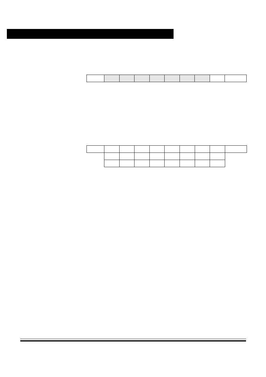
Motorola Interconnect Bus (MI BUS)
Technical Data
MC68HC11P2 -- Rev 1.0
122
Motorola Interconnect Bus (MI BUS)
MOTOROLA
6.10.6 S2SR2 -- MI BUS2 status register 2
RAF -- Receiver active flag (read only)
1 = A character is being received.
0 = A character is not being received.
6.10.7 S2DRL -- MI BUS2 data register
This register forms the 8-bit data/address word for the MI push field and
contains the 3-bit data word received as the MI pull field.
R/T[7:0] -- Receiver/transmitter data bits [7:0]
READ: Reads access the three bits of pull field data (stored in bits
3≠1) of the read-only MI BUS receive data register. Bits [7:4, 0] are a
fixed data pattern when a valid status and end-of-frame is returned. A
valid status is represented by the following data pattern: 0101 xxx1
(bits 7≠0), where `xxx' is the status. All ones in the receive data
register indicate that an error occurred on the MI BUS. Bits are
received LSB first by the MCU, and the status bits map as shown in
the above table.
WRITE: Writes access the eight bits of the write-only MI BUS transmit
data register. MI BUS devices require a 5-bit data pattern followed by
a 3-bit address pattern to be sent during the push field. The data
pattern is mapped to the lowest five bits of the data register and the
address to the highest three bits, as shown in the above table. Thus
MI-data[4:0] is written to S2DRL[4:0] and MI-address[2:0] is written to
S2DRL[7:5].
Address bit 7
bit 6
bit 5
bit 4
bit 3
bit 2
bit 1
bit 0
State
on reset
SCI/MI 2 status 2 (S2SR2)
$0055
0
0
0
0
0
0
0
RAF2 0000 0000
Address bit 7
bit 6
bit 5
bit 4
bit 3
bit 2
bit 1
bit 0
State
on reset
SCI/MI 2 data low (S2DRL)
$0057 R7T7B R6T6B R5T5B R4T4B R3T3B R2T2B R1T1B R0T0B undefined
0
1
0
1
S1
S2
S3
1
Pull field
A2
A1
A0
D4
D3
D2
D1
D0
Push field

Motorola Interconnect Bus (MI BUS)
SCI/MI BUS3 registers
MC68HC11P2 -- Rev 1.0
Technical Data
MOTOROLA
Motorola Interconnect Bus (MI BUS)
123
6.11 SCI/MI BUS3 registers
The MI BUS2 and MI BUS3 modules share the MI BUS delay register
(INIT2) at $0037 and the MI BUS2 clock rate register (S2BDH/L) at
$0050≠51. The two modules are functionally identical to one another
and the registers for MI BUS3 are given here for reference purposes
only. All explanations of bit function can be found in the relevant section
of the MI BUS2 register descriptions.
6.11.1 S3CR1 -- MI BUS3 control register 1
6.11.2 S3CR2 -- MI BUS3 control register 2
6.11.3 S3SR1 -- MI BUS3 status register 1
6.11.4 S3SR2 -- MI BUS3 status register 2
Address bit 7
bit 6
bit 5
bit 4
bit 3
bit 2
bit 1
bit 0
State
on reset
SCI/MI 3 control 1 (S3CR1)
$005A LOPS3WOMS3 MIE3
M3
WAKE3 ILT3
PE3
PT3 0000 0000
Address bit 7
bit 6
bit 5
bit 4
bit 3
bit 2
bit 1
bit 0
State
on reset
SCI/MI 3 control 2 (S3CR2)
$005B
TIE3 TCIE3 RIE3
ILIE3
TE3
RE3
RWU3 SBK3 0000 0000
Address bit 7
bit 6
bit 5
bit 4
bit 3
bit 2
bit 1
bit 0
State
on reset
SCI/MI 3 status 1 (S3SR1)
$005C TDRE3 TC3 RDRF3 IDLE3
OR3
NF3
FE3
PF3 1100 0000
Address bit 7
bit 6
bit 5
bit 4
bit 3
bit 2
bit 1
bit 0
State
on reset
SCI/MI 3 status 2 (S3SR2)
$005D
0
0
0
0
0
0
0
RAF3 0000 0000

Motorola Interconnect Bus (MI BUS)
Technical Data
MC68HC11P2 -- Rev 1.0
124
Motorola Interconnect Bus (MI BUS)
MOTOROLA
6.11.5 S3DRL -- MI BUS3 data register
Address bit 7
bit 6
bit 5
bit 4
bit 3
bit 2
bit 1
bit 0
State
on reset
SCI/MI 3 data low (S3DRL)
$005F R7T7C R6T6C R5T5C R4T4C R3T3C R2T2C R1T1C R0T0C undefined
0
1
0
1
S1
S2
S3
1
Pull field
A2
A1
A0
D4
D3
D2
D1
D0
Push field

MC68HC11P2 -- Rev 1.0
Technical Data
MOTOROLA
Serial Peripheral Interface (SPI)
125
Technical Data -- MC68HC11P2
Section 7. Serial Peripheral Interface (SPI)
7.1 Contents
7.2
Introduction. . . . . . . . . . . . . . . . . . . . . . . . . . . . . . . . . . . . . . 125
7.3
Functional description . . . . . . . . . . . . . . . . . . . . . . . . . . . . .126
7.4
SPI transfer formats . . . . . . . . . . . . . . . . . . . . . . . . . . . . . . . 126
7.5
SPI signals. . . . . . . . . . . . . . . . . . . . . . . . . . . . . . . . . . . . . . . 129
7.6
SPI system errors . . . . . . . . . . . . . . . . . . . . . . . . . . . . . . . . . 130
7.7
SPI registers . . . . . . . . . . . . . . . . . . . . . . . . . . . . . . . . . . . . . 132
7.2 Introduction
The serial peripheral interface (SPI), an independent serial
communications subsystem, allows the MCU to communicate
synchronously with peripheral devices, such as transistor-transistor
logic (TTL) shift registers, liquid crystal (LCD) display drivers, analog-to-
digital converter subsystems, and other microprocessors. The SPI is
also capable of inter-processor communication in a multiple master
system. The SPI system can be configured as either a master or a slave
device, with data rates as high as one half of the E clock rate when
configured as a master and as fast as the E clock rate when configured
as a slave.
The SPI shares I/O with four of port D's pins and is enabled by SPE in
the SPCR:

Serial Peripheral Interface (SPI)
Technical Data
MC68HC11P2 -- Rev 1.0
126
Serial Peripheral Interface (SPI)
MOTOROLA
7.3 Functional description
The central element in the SPI system is the block containing the shift
register and the read data buffer (see
Figure 7-1
). The system is single
buffered in the transmit direction and double buffered in the receive
direction. This means that new data for transmission cannot be written
to the shifter until the previous transfer is complete; however, received
data is transferred into a parallel read data buffer so the shifter is free to
accept a second serial character. As long as the first character is read
out of the read data buffer before the next serial character is ready to be
transferred, no overrun condition occurs. A single MCU register address
is used for reading data from the read data buffer and for writing data to
the shifter.
The SPI status block represents the SPI status functions (transfer
complete, write collision, and mode fault) performed by the serial
peripheral status register (SPSR). The SPI control block represents
those functions that control the SPI system through the serial peripheral
control register (SPCR).
7.4 SPI transfer formats
During an SPI transfer, data is simultaneously transmitted and received.
A serial clock line synchronizes shifting and sampling of the information
on the two serial data lines. A slave select line allows individual selection
of a slave SPI device; slave devices that are not selected do not interfere
with SPI bus activities. On a master SPI device, the select line can
Pin
Alternate
function
PD2
MISO
PD3
MOSI
PD4
SCK
PD5
SS
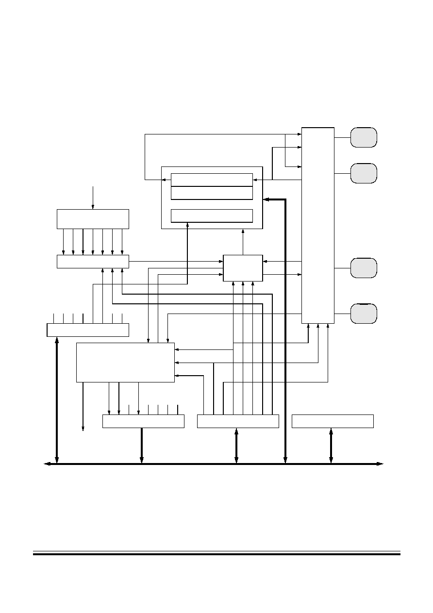
Serial Peripheral Interface (SPI)
SPI transfer formats
MC68HC11P2 -- Rev 1.0
Technical Data
MOTOROLA
Serial Peripheral Interface (SPI)
127
optionally be used to indicate a multiple master bus contention. Refer to
Figure 7-2
.
Figure 7-1. SPI block diagram
SPCR ≠ SPI control register
SPSR ≠ SPI status register
Divider
SPDR ≠ SPI data register
Shift control logic
Read data buffer
8-bit shift register
OPT2 ≠ Options register 2
˜2
˜4
˜8
˜16 ˜32 ˜64 ˜128
Select
Clock
logic
SPI control
MISO
PD2
MOSI
PD3
SCK
PD4
SS
PD5
S
M
S
M
S
M
Pin
control
logic
MCU
system clock
SP
I
E
SP
E
DW
O
M
MS
TR
CP
O
L
CP
HA
SP
R1
SP
R0
SP
I
F
WC
O
L
MO
DF
LS
BF
SP
R2
MS
TR
SP
E
DW
O
M
MSTR
SPE
SPIE
LS
BF
Cl
oc
k
SPI clock (master)
SPI interrupt
request
Internal bus
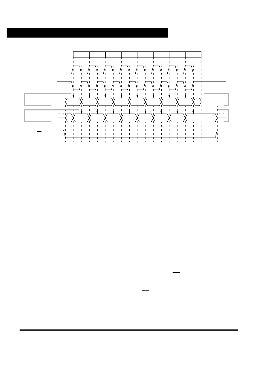
Serial Peripheral Interface (SPI)
Technical Data
MC68HC11P2 -- Rev 1.0
128
Serial Peripheral Interface (SPI)
MOTOROLA
7.4.1 Clock phase and polarity controls
Software can select one of four combinations of serial clock phase and
polarity using two bits in the SPI control register (SPCR). The clock
polarity is specified by the CPOL control bit, which selects an active high
or active low clock, and has no significant effect on the transfer format.
The clock phase (CPHA) control bit selects one of two different transfer
formats. The clock phase and polarity should be identical for the master
SPI device and the communicating slave device. In some cases, the
phase and polarity are changed between transfers to allow a master
device to communicate with peripheral slaves having different
requirements.
When CPHA equals zero, the SS line must be deasserted and
reasserted between each successive serial byte. Also, if the slave writes
data to the SPI data register (SPDR) while SS is low, a write collision
error results.
When CPHA equals one, the SS line can remain low between
successive transfers.
Figure 7-2. SPI transfer format
1
2
3
4
5
6
7
8
MSB
6
5
4
3
2
1
LSB
MSB
6
5
4
3
2
1
LSB
SCK cycle #
(for reference)
SCK (CPOL=0)
SCK (CPOL=1)
Sample input
Data out (CPHA=0)
Sample input
Data out (CPHA=1)
SS (to slave)
Note: this figure shows the LSBF=0 (default) case. If LSBF=1, data is transferred in the reverse order (LSB first).

Serial Peripheral Interface (SPI)
SPI signals
MC68HC11P2 -- Rev 1.0
Technical Data
MOTOROLA
Serial Peripheral Interface (SPI)
129
7.5 SPI signals
The following paragraphs contain descriptions of the four SPI signals:
master in slave out (MISO), master out slave in (MOSI), serial clock
(SCK), and slave select (SS).
Any SPI output line must have its corresponding data direction bit in
DDRD register set. If the DDR bit is clear, that line is disconnected from
the SPI logic and becomes a general-purpose input. All SPI input lines
are forced to act as inputs regardless of the state of the corresponding
DDR bits in DDRD register.
7.5.1 Master in slave out
MISO is one of two unidirectional serial data signals. It is an input to a
master device and an output from a slave device. The MISO line of a
slave device is placed in the high-impedance state if the slave device is
not selected.
7.5.2 Master out slave in
The MOSI line is the second of the two unidirectional serial data signals.
It is an output from a master device and an input to a slave device. The
master device places data on the MOSI line a half-cycle before the clock
edge that the slave device uses to latch the data.
7.5.3 Serial clock
SCK, an input to a slave device, is generated by the master device and
synchronizes data movement in and out of the device through the MOSI
and MISO lines. Master and slave devices are capable of exchanging a
byte of information during a sequence of eight clock cycles.
There are four possible timing relationships that can be chosen by using
control bits CPOL and CPHA in the serial peripheral control register
(SPCR). Both master and slave devices must operate with the same
timing. The SPI clock rate select bits, SPR[1:0], in the SPCR of the

Serial Peripheral Interface (SPI)
Technical Data
MC68HC11P2 -- Rev 1.0
130
Serial Peripheral Interface (SPI)
MOTOROLA
master device, select the clock rate. In a slave device, SPR[1:0] have no
effect on the operation of the SPI.
7.5.4 Slave select
The slave select SS input of a slave device must be externally asserted
before a master device can exchange data with the slave device. SS
must be low before data transactions begin and must stay low for the
duration of the transaction.
The SS line of the master must be held high. If it goes low, a mode fault
error flag (MODF) is set in the serial peripheral status register (SPSR).
To disable the mode fault circuit, write a one in bit 5 of the port D data
direction register. This sets the SS pin to act as a general-purpose
output, rather than a dedicated input to the slave select circuit, thus
inhibiting the mode fault flag. The other three lines are dedicated to the
SPI whenever the serial peripheral interface is on.
The state of the master and slave CPHA bits affects the operation of SS.
CPHA settings should be identical for master and slave. When CPHA =
0, the shift clock is the OR of SS with SCK. In this clock phase mode, SS
must go high between successive characters in an SPI message. When
CPHA = 1, SS can be left low between successive SPI characters. In
cases where there is only one SPI slave MCU, its SS line can be tied to
V
SS
as long as only CPHA = 1 clock mode is used.
7.6 SPI system errors
Two kinds of system errors can be detected by the SPI system. The first
type of error arises in a multiple-master system when more than one SPI
device simultaneously tries to be a master. This error is called a mode
fault. The second type of error, write collision, indicates that an attempt
was made to write data to the SPDR while a transfer was in progress.
When the SPI system is configured as a master and the SS input line
goes to active low, a mode fault error has occurred -- usually because
two devices have attempted to act as master at the same time. In the
case where more than one device is concurrently configured as a

Serial Peripheral Interface (SPI)
SPI system errors
MC68HC11P2 -- Rev 1.0
Technical Data
MOTOROLA
Serial Peripheral Interface (SPI)
131
master, there is a chance of contention between two pin drivers. For
push-pull CMOS drivers, this contention can cause permanent damage.
The mode fault detection circuitry attempts to protect the device by
disabling the drivers. The MSTR control bit in the SPCR and all four
DDRD control bits associated with the SPI are cleared and an interrupt
is generated (subject to masking by the SPIE control bit and the I bit in
the CCR).
Other precautions may need to be taken to prevent driver damage. If two
devices are made masters at the same time, the mode fault detector
does not help protect either one unless one of them selects the other as
slave. The amount of damage possible depends on the length of time
both devices attempt to act as master.
A write collision error occurs if the SPDR is written while a transfer is in
progress. Because the SPDR is not double buffered in the transmit
direction, writes to SPDR cause data to be written directly into the SPI
shift register. Because this write corrupts any transfer in progress, a
write collision error is generated. The transfer continues undisturbed,
and the write data that caused the error is not written to the shifter.
A write collision is normally a slave error because a slave has no control
over when a master initiates a transfer. A master knows when a transfer
is in progress, so there is no reason for a master to generate a write-
collision error, although the SPI logic can detect write collisions in both
master and slave devices.
The SPI configuration determines the characteristics of a transfer in
progress. For a master, a transfer begins when data is written to SPDR
and ends when SPIF is set. For a slave with CPHA equal to zero, a
transfer starts when SS goes low and ends when SS returns high. In this
case, SPIF is set at the middle of the eighth SCK cycle when data is
transferred from the shifter to the parallel data register, but the transfer
is still in progress until SS goes high. For a slave with CPHA equal to
one, transfer begins when the SCK line goes to its active level, which is
the edge at the beginning of the first SCK cycle. The transfer ends when
SPIF is set, for a slave in which CPHA=1.

Serial Peripheral Interface (SPI)
Technical Data
MC68HC11P2 -- Rev 1.0
132
Serial Peripheral Interface (SPI)
MOTOROLA
7.7 SPI registers
The three SPI registers, SPCR, SPSR, and SPDR, provide control,
status, and data storage functions. Refer to the following information for
a description of how these registers are organized.
7.7.1 SPCR -- Serial peripheral control register
SPIE -- Serial peripheral interrupt enable
1 = A hardware interrupt sequence is requested each time SPIF or
MODF is set.
0 = SPI interrupts are inhibited.
Set the SPIE bit to a one to request a hardware interrupt sequence
each time the SPIF or MODF status flag is set. SPI interrupts are
inhibited if this bit is clear or if the I bit in the condition code register is
one.
SPE -- Serial peripheral system enable
1 = Port D [5:2] is dedicated to the SPI.
0 = Port D has its default I/O functions.
When the SPE bit is set, the port D pins 2, 3, 4, and 5 are dedicated
to the SPI functions and lose their general purpose I/O functions.
When the SPI system is enabled and expects any of PD[4:2] to be
inputs then those pins will be inputs regardless of the state of the
associated DDRD bits. If any of PD[4:2] are expected to be outputs
then those pins will be outputs only if the associated DDRD bits are
set. However, if the SPI is in the master mode, DDD5 determines
whether PD5 is an error detect input (DDD5 = 0) or a general-purpose
output (DDD5 = 1).
DWOM -- Port D wired-OR mode
1 = Port D [5:2] buffers configured for open-drain outputs.
0 = Port D [5:2] buffers configured for normal CMOS outputs.
Address bit 7
bit 6
bit 5
bit 4
bit 3
bit 2
bit 1
bit 0
State
on reset
SPI control (SPCR)
$0028
SPIE
SPE DWOM MSTR CPOL CPHA SPR1 SPR0 0000 01uu

Serial Peripheral Interface (SPI)
SPI registers
MC68HC11P2 -- Rev 1.0
Technical Data
MOTOROLA
Serial Peripheral Interface (SPI)
133
MSTR -- Master mode select
1 = Master mode
0 = Slave mode
CPOL -- Clock polarity
1 = SCK is active low.
0 = SCK is active high.
When the clock polarity bit is cleared and data is not being
transferred, the SCK pin of the master device has a steady state low
value. When CPOL is set, SCK idles high. Refer to
Figure 7-2
and
Clock phase and polarity controls
.
CPHA -- Clock phase
The clock phase bit, in conjunction with the CPOL bit, controls the
clock-data relationship between master and slave. The CPHA bit
selects one of two different clocking protocols. Refer to
Figure 7-2
and
Clock phase and polarity controls
.
SPR1 and SPR0 -- SPI clock rate selects
These two bits select the SPI clock rate, as shown in
Table 7-1
. Note
that SPR2 is located in the OPT2 register and its state on reset is
zero.
Table 7-1. SPI clock rates
SPR[2:0]
E clock
divide ratio
SPI clock frequency (
baud rate) for:
E = 2 MHz
E = 3 MHz
E = 4 MHz
0 0 0
2
1.0 MHz
1.5 MHz
2.0 MHz
0 0 1
4
500 kHz
750kHz
1.0 MHz
0 1 0
16
125 kHz
187.5 kHz
250 kHz
0 1 1
32
62.5 kHz
93.7 kHz
125 kHz
1 0 0
8
250 kHz
375 kHz
500 kHz
1 0 1
16
125 kHz
187.5 kHz
250 kHz
1 1 0
64
31.3 kHz
46.9 kHz
62.5 kHz
1 1 1
128
15.6 kHz
23.4 kHz
31.3 kHz

Serial Peripheral Interface (SPI)
Technical Data
MC68HC11P2 -- Rev 1.0
134
Serial Peripheral Interface (SPI)
MOTOROLA
7.7.2 SPSR -- Serial peripheral status register
SPIF -- SPI interrupt complete flag
1 = Data transfer to external device has been completed.
0 = No valid completion of data transfer.
SPIF is set upon completion of data transfer between the processor
and the external device. If SPIF goes high, and if SPIE is set, a serial
peripheral interrupt is generated. To clear the SPIF bit, read the SPSR
with SPIF set, then access the SPDR. Unless SPSR is read (with
SPIF set) first, attempts to write SPDR are inhibited.
WCOL -- Write collision
1 = Write collision.
0 = No write collision.
Clearing the WCOL bit is accomplished by reading the SPSR (with
WCOL set) followed by an access of SPDR. Refer to
Slave select
and
SPI system errors
.
MODF -- Mode fault
1 = Mode fault.
0 = No mode fault.
To clear the MODF bit, read the SPSR (with MODF set), then write to
the SPCR. Refer to
Slave select
and
SPI system errors
.
Bits [5, 3:0] -- Not implemented; always read zero.
Address bit 7
bit 6
bit 5
bit 4
bit 3
bit 2
bit 1
bit 0
State
on reset
SPI status (SPSR)
$0029
SPIF WCOL
0
MODF
0
0
0
0
0000 0000

Serial Peripheral Interface (SPI)
SPI registers
MC68HC11P2 -- Rev 1.0
Technical Data
MOTOROLA
Serial Peripheral Interface (SPI)
135
7.7.3 SPDR -- SPI data register
The SPDR is used when transmitting or receiving data on the serial bus.
Only a write to this register initiates transmission or reception of a byte,
and this only occurs in the master device. At the completion of
transferring a byte of data, the SPIF status bit is set in both the master
and slave devices.
A read of the SPDR is actually a read of a buffer. To prevent an overrun
and the loss of the byte that caused the overrun, the first SPIF must be
cleared by the time a second transfer of data from the shift register to the
read buffer is initiated.
SPI is double buffered in and single buffered out.
7.7.4 OPT2 -- System configuration options register 2
LIRDV -- LIR driven (refer to
Operating Modes and On-Chip Memory
)
1 = Enable LIR drive high pulse.
0 = LIR only driven low ≠ requires pull-up on pin.
CWOM -- Port C wired-OR mode (refer to
Parallel Input/Output
)
1 = Port C outputs are open-drain.
0 = Port C operates normally.
STRCH -- Stretch external accesses (refer to
Operating Modes and
On-Chip Memory
)
1 = Off-chip accesses are extended by one E clock cycle.
0 = Normal operation.
Address bit 7
bit 6
bit 5
bit 4
bit 3
bit 2
bit 1
bit 0
State
on reset
SPI data (SPDR)
$002A
(bit 7)
(6)
(5)
(4)
(3)
(2)
(1)
(bit 0)
not
affected
Address bit 7
bit 6
bit 5
bit 4
bit 3
bit 2
bit 1
bit 0
State
on reset
System config. options 2 (OPT2) $0038 LIRDV CWOM
STRC
H
IRVNE LSBF SPR2
0
0
000x 0000

Serial Peripheral Interface (SPI)
Technical Data
MC68HC11P2 -- Rev 1.0
136
Serial Peripheral Interface (SPI)
MOTOROLA
IRVNE -- Internal read visibility/not E (refer to
Operating Modes and
On-Chip Memory
)
1 = Data from internal reads is driven out of the external data bus.
0 = No visibility of internal reads on external bus.
In single chip mode this bit determines whether the E clock drives
out from the chip.
1 = E pin is driven low.
0 = E clock is driven out from the chip.
LSBF -- LSB first enable
1 = Data is transferred LSB first.
0 = Data is transferred MSB first.
If this bit is set, data, which is usually transferred MSB first, is
transferred LSB first. LSBF does not affect the position of the MSB
and LSB in the data register. Reads and writes of the data register
always have MSB in bit 7.
SPR2 -- SPI clock rate select
When set, SPR2 adds a divide-by-4 prescaler to the SPI clock chain.
With the two bits in the SPCR, this bit specifies the SPI clock rate.
Refer to
Table 7-1
.
Bits 1, 0 -- not implemented; always read zero.

MC68HC11P2 -- Rev 1.0
Technical Data
MOTOROLA
Timing System
137
Technical Data -- MC68HC11P2
Section 8. Timing System
8.1 Contents
8.2
Introduction. . . . . . . . . . . . . . . . . . . . . . . . . . . . . . . . . . . . . . 137
8.3
Timer structure . . . . . . . . . . . . . . . . . . . . . . . . . . . . . . . . . . . 139
8.4
Input capture . . . . . . . . . . . . . . . . . . . . . . . . . . . . . . . . . . . . . 142
8.5
Output compare . . . . . . . . . . . . . . . . . . . . . . . . . . . . . . . . . . 145
8.6
Real-time interrupt . . . . . . . . . . . . . . . . . . . . . . . . . . . . . . . . 154
8.7
Computer operating properly watchdog function . . . . . . . 157
8.8
Pulse accumulator . . . . . . . . . . . . . . . . . . . . . . . . . . . . . . . . 158
8.9
Pulse-width modulation (PWM) timer . . . . . . . . . . . . . . . . . 162
8.2 Introduction
The M68HC11 timing system is composed of five clock divider chains.
The main clock divider chain includes a 16-bit free-running counter,
which is driven by a programmable prescaler. The main timer's
programmable prescaler provides one of the four clocking rates to drive
the 16-bit counter. Two prescaler control bits select the prescale rate.
The prescaler output divides the system clock by 1, 4, 8, or 16. Taps
from this main clocking chain drive circuitry generate the slower clocks
used by the pulse accumulator, the real-time interrupt (RTI), and the
computer operating properly (COP) watchdog subsystems, which are
also described in this section. Refer to
Figure 8-1
.
All main timer system activities are referenced to this free-running
counter. The counter begins incrementing from $0000 as the MCU
comes out of reset, and continues to the maximum count, $FFFF. At the

Timing System
Technical Data
MC68HC11P2 -- Rev 1.0
138
Timing System
MOTOROLA
maximum count, the counter rolls over to $0000, sets an overflow flag
and continues to increment. As long as the MCU is running in a normal
operating mode, there is no way to reset, change or interrupt the
counting. The capture/compare subsystem features three input capture
channels, four output compare channels and one channel that can be
selected to perform either input capture or output compare. Each of the
three input capture functions has its own 16-bit input capture register
(time capture latch) and each of the output compare functions has its
own 16-bit compare register. All timer functions, including the timer
overflow and RTI, have their own interrupt controls and separate
interrupt vectors.
The pulse accumulator contains an 8-bit counter and edge select logic.
The pulse accumulator can operate in either event counting mode or
gated time accumulation mode. During event counting mode, the pulse
accumulator's 8-bit counter increments when a specified edge is
detected on an input signal. During gated time accumulation mode, an
internal clock source increments the 8-bit counter while an input signal
has a predetermined logic level.
The real-time interrupt (RTI) is a programmable periodic interrupt circuit
that permits pacing the execution of software routines by selecting one
of four interrupt rates.
The COP watchdog clock input (E/2
15
) is tapped off from the free-
running counter chain. The COP automatically times out unless it is
serviced within a specific time by a program reset sequence. If the COP
is allowed to time out, a reset is generated, which drives the RESET pin
low to reset the MCU and the external system. Refer to
Table 8-1
for
crystal related frequencies and periods.

Timing System
Timer structure
MC68HC11P2 -- Rev 1.0
Technical Data
MOTOROLA
Timing System
139
8.3 Timer structure
The timer functions share I/O with all eight pins of port A:
Figure 8-2
shows the capture/compare system block diagram. The port
A pin control block includes logic for timer functions and for general-
purpose I/O. For pins PA3, PA2, PA1 and PA0, this block contains both
the edge-detection logic and the control logic that enables the selection
of which edge triggers an input capture. The digital level on PA[3:0] can
be read at any time (read PORTA register), even if the pin is being used
for the input capture function. Pins PA[6:3] are used either for general-
purpose I/O, or as output compare pins. When one of these pins is being
Table 8-1. Timer resolution and capacity
Clock
4.0MHz
8.0MHz
12.0 MHz
16.0MHz
4E
XTAL
Control bits
PR[1:0]
1.0MHz
2.0MHz
3.0 MHz
4.0 MHz
E
E clock
1 000 ns
500ns
333ns
250ns
1/E
Period
0 0
1.0µs
65.536ms
500 ns
32.768ms
333 ns
21.845ms
250ns
16.384ms
1/E
2
16
/E
≠ resolution
≠ overflow
0 1
4.0µs
262.14ms
2.0µs
131.07ms
1.333µs
87.381ms
1.0µs
65.536ms
4/E
2
18
/E
≠ resolution
≠ overflow
1 0
8.0µs
524.29ms
4.0µs
262.14ms
2.667µs
174.76ms
2.0µs
131.07ms
8/E
2
19
/E
≠ resolution
≠ overflow
1 1
16.0µs
1049 ms
8.0µs
524.29ms
5.333µs
349.53ms
4.0µs
262.14ms
16/E
2
20
/E
≠ resolution
≠ overflow
Pin
Alternate function
PA0
IC3
PA1
IC2
PA2
IC1
PA3
OC5 and/or OC1, or IC4
PA4
OC4 and/or OC1
PA5
OC3 and/or OC1
PA6
OC2 and/or OC1
PA7
PAI and/or OC1

Timing System
Technical Data
MC68HC11P2 -- Rev 1.0
140
Timing System
MOTOROLA
used for an output compare function, it cannot be written directly as if it
were a general-purpose output. Each of the output compare functions
(OC[5:2]) is related to one of the port A output pins. Output compare 1
(OC1) has extra control logic, allowing it optional control of any
combination of the PA[7:3] pins. The PA7 pin can be used as a general-
purpose I/O pin, as an input to the pulse accumulator or as an OC1
output pin.
Figure 8-1. Timer clock divider chains
Set
Q
Q
Reset
FF1
+
Oscillator and
clock generator
˜
2
˜
2
˜
4
Baud
˜
1, 2, 3, 4, 5,..., 8191
SCI receiver clock
˜
16
SCI transmitter clock
E clock
Prescaler
˜
2, 4, 8,16, 32, 64, 128
SPR[2:0]
Internal bus clock (PH2)
SPI
E/2
6
E/2
13
Pulse accumulator
Prescaler
˜
1, 2, 4, 8
RTR[1:0]
Real time interrupt
˜
4
Prescaler
˜
1, 4, 8, 16
PR[1:0]
TCNT
TOF
Prescaler
˜
1, 4, 16, 64
CR[1:0]
Set
Q
Q
Reset
FF2
System reset
Clear COP timer
Force COP reset
E/2
15
IC/OC

Timing System
Timer structure
MC68HC11P2 -- Rev 1.0
Technical Data
MOTOROLA
Timing System
141
Figure 8-2. Capture/compare block diagram
+
&
Prescaler
˜
1, 4, 8, 16
PR[1:0]
MCU
E clock
16-bit
free running counter
TCNT (hi) TCNT (lo)
TOC1 (lo)
&
9
TOC1 (hi)
16-bit comparator
EQ
TOC2 (lo)
TOC2 (hi)
16-bit comparator
EQ
TOC3 (lo)
TOC3 (hi)
16-bit comparator
EQ
TOC4 (lo)
TOC4 (hi)
16-bit comparator
EQ
TI4/O5 (lo)
TI4/O5 (hi)
16-bit comparator
EQ
TIC1 (lo)
TIC1 (hi)
TIC2 (lo)
TIC2 (hi)
TIC3 (lo)
TIC3 (hi)
16-bit timer bus
16-bit latch
CLK
16-bit latch
CLK
16-bit latch
CLK
16-bit latch
CLK
OC1F
TOF
TOI
I4/O5F
8
OC2F
OC3F
OC4F
IC1F
IC2F
IC3F
I4/O5
OC5
IC4
OC1I
FOC1
Bit 7
+
&
7
OC2I
FOC2
+
&
6
OC3I
FOC3
+
&
5
OC4I
FOC4
+
&
4
I4/O5I
FOC5
&
IC1I
3
&
IC3I
1
&
IC2I
2
Bit 6
Bit 5
Bit 4
Bit 3
Bit 2
Bit 1
Bit 0
PA6/
OC2/
OC1
PA5/
OC3/
OC1
PA4/
OC4/
OC1
PA3/
OC5/
OC1/
PA2/
IC1
IC4
PA1/
IC2
PA0/
IC3
TFLG1
status
flags
TMSK1
interrupt
enables
Port A
pin
control
Port A pin actions are controlled by OC1M, OC1D, PACTL, TCTL1 and TCTL2 registers
Pins/
functions
CFORC
Force O/P
compare
To pulse accumulator
Taps for RTI, COP and PA
Note
Interrupt requests 1≠9 (these are further qualified by the I-bit in the CCR)
PA7/
OC1/
PAI

Timing System
Technical Data
MC68HC11P2 -- Rev 1.0
142
Timing System
MOTOROLA
8.4 Input capture
The input capture function records the time an external event occurs by
latching the value of the free-running counter when a selected edge is
detected at the associated timer input pin. Software can store latched
values and use them to compute the periodicity and duration of events.
For example, by storing the times of successive edges of an incoming
signal, software can determine the period and pulse width of a signal. To
measure period, two successive edges of the same polarity are
captured. To measure pulse width, two alternate polarity edges are
captured.
In most cases, input capture edges are asynchronous with respect to the
internal timer counter, which is clocked relative to an internal clock
(PH2). These asynchronous capture requests are synchronized with
PH2 so that latching occurs on the opposite half cycle of PH2 from when
the timer counter is being incremented. This synchronization process
introduces a delay from when the edge occurs to when the counter value
is detected. Because these delays cancel out when the time between
two edges is being measured, the delay can be ignored. When an input
capture is being used with an output compare, there is a similar delay
between the actual compare point and when the output pin changes
state.
The control and status bits that implement the input capture functions
are contained in the PACTL, TCTL2, TMSK1, and TFLG1 registers.
To configure port A bit 3 as an input capture, clear the DDA3 bit of the
DDRA register. Note that this bit is cleared out of reset. To enable PA3
as the fourth input capture, set the I4/O5 bit in the PACTL register.
Otherwise, PA3 is configured as a fifth output compare out of reset, with
bit I4/O5 being cleared. If the DDA3 bit is set (configuring PA3 as an
output), and IC4 is enabled, then writes to PA3 cause edges on the pin
to result in input captures. Writing to TI4/O5 has no effect when the
TI4/O5 register is acting as IC4.

Timing System
Input capture
MC68HC11P2 -- Rev 1.0
Technical Data
MOTOROLA
Timing System
143
8.4.1 TCTL2 -- Timer control register 2
Use the control bits of this register to program input capture functions to
detect a particular edge polarity on the corresponding timer input pin.
Each of the input capture functions can be independently configured to
detect rising edges only, falling edges only, any edge (rising or falling),
or to disable the input capture function. The input capture functions
operate independently of each other and can capture the same TCNT
value if the input edges are detected within the same timer count cycle.
EDGxB and EDGxA -- Input capture edge control
There are four pairs of these bits. Each pair is cleared by reset and
must be encoded to configure the corresponding input capture edge
detector circuit. IC4 functions only if the I4/O5 bit in the PACTL
register is set.
Address bit 7
bit 6
bit 5
bit 4
bit 3
bit 2
bit 1
bit 0
State
on reset
Timer control 2 (TCTL2)
$0021 EDG4BEDG4AEDG1BEDG1AEDG2BEDG2AEDG3BEDG3A 0000 0000
EDGxB
EDGxA
Configuration
0
0
ICx disabled
0
1
ICx captures on rising edges only
1
0
ICx captures on falling edges only
1
1
ICx captures on any edge

Timing System
Technical Data
MC68HC11P2 -- Rev 1.0
144
Timing System
MOTOROLA
8.4.2 TIC1≠TIC3 -- Timer input capture registers
When an edge has been detected and synchronized, the 16-bit free-
running counter value is transferred into the input capture register pair
as a single 16-bit parallel transfer. Timer counter value captures and
timer counter incrementing occur on opposite half-cycles of the phase 2
clock so that the count value is stable whenever a capture occurs. Input
capture values can be read from a pair of 8-bit read-only registers. A
read of the high-order byte of an input capture register pair inhibits a new
capture transfer for one bus cycle. If a double-byte read instruction, such
as LDD, is used to read the captured value, coherency is assured. When
a new input capture occurs immediately after a high-order byte read,
transfer is delayed for an additional cycle but the value is not lost.
The TICx registers are not affected by reset.
Address bit 7
bit 6
bit 5
bit 4
bit 3
bit 2
bit 1
bit 0
State
on reset
Timer input capture 1 (TIC1) high $0010 (bit 15)
(14)
(13)
(12)
(11)
(10)
(9)
(bit 8)
not
affected
Timer input capture 1 (TIC1) low
$0011
(bit 7)
(6)
(5)
(4)
(3)
(2)
(1)
(bit 0)
not
affected
Timer input capture 2 (TIC2) high $0012 (bit 15)
(14)
(13)
(12)
(11)
(10)
(9)
(bit 8)
not
affected
Timer input capture 2 (TIC2) low
$0013
(bit 7)
(6)
(5)
(4)
(3)
(2)
(1)
(bit 0)
not
affected
Timer input capture 3 (TIC3) high $0014 (bit 15)
(14)
(13)
(12)
(11)
(10)
(9)
(bit 8)
not
affected
Timer input capture 3 (TIC3) low
$0015
(bit 7)
(6)
(5)
(4)
(3)
(2)
(1)
(bit 0)
not
affected

Timing System
Output compare
MC68HC11P2 -- Rev 1.0
Technical Data
MOTOROLA
Timing System
145
8.4.3 TI4/O5 -- Timer input capture 4/output compare 5 register
Use TI4/O5 as either an input capture register or an output compare
register, depending on the function chosen for the PA3 pin. To enable it
as an input capture pin, set the I4/O5 bit in the pulse accumulator control
register (PACTL) to logic level one. To use it as an output compare
register, set the I4/O5 bit to a logic level zero. Refer to
PACTL -- Pulse
accumulator control register
.
The TI4/O5 register pair resets to ones ($FFFF).
8.5 Output compare
Use the output compare (OC) function to program an action to occur at
a specific time -- when the 16-bit counter reaches a specified value. For
each of the five output compare functions, there is a separate 16-bit
compare register and a dedicated 16-bit comparator. The value in the
compare register is compared to the value of the free-running counter on
every bus cycle. When the compare register matches the counter value,
an output compare status flag is set. The flag can be used to initiate the
automatic actions for that output compare function.
To produce a pulse of a specific duration, write a value to the output
compare register that represents the time the leading edge of the pulse
is to occur. The output compare circuit is configured to set the
appropriate output either high or low, depending on the polarity of the
pulse being produced. After a match occurs, the output compare register
is reprogrammed to change the output pin back to its inactive level at the
next match. A value representing the width of the pulse is added to the
original value, and then written to the output compare register. Because
the pin state changes occur at specific values of the free-running
counter, the pulse width can be controlled accurately at the resolution of
Address bit 7
bit 6
bit 5
bit 4
bit 3
bit 2
bit 1
bit 0
State
on reset
Capture 4/compare 5 (TI4/O5)
high
$001E (bit 15) (14)
(13)
(12)
(11)
(10)
(9)
(bit 8) 1111 1111
Capture 4/compare 5 (TI4/O5)
low
$001F
(bit 7)
(6)
(5)
(4)
(3)
(2)
(1)
(bit 0) 1111 1111

Timing System
Technical Data
MC68HC11P2 -- Rev 1.0
146
Timing System
MOTOROLA
the free-running counter, independent of software latency. To generate
an output signal of a specific frequency and duty cycle, repeat this pulse-
generating procedure.
There are four 16-bit read/write output compare registers: TOC1, TOC2,
TOC3, and TOC4, and the TI4/O5 register, which functions under
software control as either IC4 or OC5. Each of the OC registers is set to
$FFFF on reset. A value written to an OC register is compared to the
free-running counter value during each E clock cycle. If a match is found,
the particular output compare flag is set in timer interrupt flag register 1
(TFLG1). If that particular interrupt is enabled in the timer interrupt mask
register 1 (TMSK1), an interrupt is generated. In addition to an interrupt,
a specified action can be initiated at one or more timer output pins. For
OC[5:2], the pin action is controlled by pairs of bits (OMx and OLx) in the
TCTL1 register. The output action is taken on each successful compare,
regardless of whether or not the OCxF flag in the TFLG1 register was
previously cleared.
OC1 is different from the other output compares in that a successful OC1
compare can affect any or all five of the OC pins. The OC1 output action
taken when a match is found is controlled by two 8-bit registers with
three bits unimplemented: the output compare 1 mask register, OC1M,
and the output compare 1 data register, OC1D. OC1M specifies which
port A outputs are to be used, and OC1D specifies what data is placed
on these port pins.

Timing System
Output compare
MC68HC11P2 -- Rev 1.0
Technical Data
MOTOROLA
Timing System
147
8.5.1 TOC1≠TOC4 -- Timer output compare registers
All output compare registers are 16-bit read-write. Each is initialized to
$FFFF at reset. If an output compare register is not used for an output
compare function, it can be used as a storage location. A write to the
high-order byte of an output compare register pair inhibits the output
compare function for one bus cycle. This inhibition prevents
inappropriate subsequent comparisons. Coherency requires a complete
16-bit read or write. However, if coherency is not needed, byte accesses
can be used.
For output compare functions, write a comparison value to output
compare registers TOC1≠TOC4 and TI4/O5. When TCNT value
matches the comparison value, specified pin actions occur.
All TOCx register pairs reset to ones ($FFFF).
Address bit 7
bit 6
bit 5
bit 4
bit 3
bit 2
bit 1
bit 0
State
on reset
Timer output compare 1 (TOC1)
high
$0016 (bit 15) (14)
(13)
(12)
(11)
(10)
(9)
(bit 8) 1111 1111
Timer output compare 1 (TOC1)
low
$0017
(bit 7)
(6)
(5)
(4)
(3)
(2)
(1)
(bit 0) 1111 1111
Timer output compare 2 (TOC2)
high
$0018 (bit 15) (14)
(13)
(12)
(11)
(10)
(9)
(bit 8) 1111 1111
Timer output compare 2 (TOC2)
low
$0019
(bit 7)
(6)
(5)
(4)
(3)
(2)
(1)
(bit 0) 1111 1111
Timer output compare 3 (TOC3)
high
$001A (bit 15) (14)
(13)
(12)
(11)
(10)
(9)
(bit 8) 1111 1111
Timer output compare 3 (TOC3)
low
$001B
(bit 7)
(6)
(5)
(4)
(3)
(2)
(1)
(bit 0) 1111 1111
Timer output compare 4 (TOC4)
high
$001C (bit 15) (14)
(13)
(12)
(11)
(10)
(9)
(bit 8) 1111 1111
Timer output compare 4 (TOC4)
low
$001D (bit 7)
(6)
(5)
(4)
(3)
(2)
(1)
(bit 0) 1111 1111

Timing System
Technical Data
MC68HC11P2 -- Rev 1.0
148
Timing System
MOTOROLA
8.5.2 CFORC -- Timer compare force register
The CFORC register allows forced early compares. FOC[1:5]
correspond to the five output compares. These bits are set for each
output compare that is to be forced. The action taken as a result of a
forced compare is the same as if there were a match between the OCx
register and the free-running counter, except that the corresponding
interrupt status flag bits are not set. The forced channels trigger their
programmed pin actions to occur at the next timer count transition after
the write to CFORC.
The CFORC bits should not be used on an output compare function that
is programmed to toggle its output on a successful compare because a
normal compare that occurs immediately before or after the force can
result in an undesirable operation.
FOC[1:5] -- Force output compares
1 = A forced output compare action will occur on the specified pin.
0 = No action.
Bits [2:0] -- Not implemented; always read zero
8.5.3 OC1M -- Output compare 1 mask register
Use OC1M with OC1 to specify the bits of port A that are affected by a
successful OC1 compare. The bits of the OC1M register correspond to
PA7≠PA3.
OC1M[7:3] -- Output compare masks for OC1
1 = OC1 is configured to control the corresponding pin of port A.
0 = OC1 will not affect the corresponding port A pin.
Bits [2:0] -- Not implemented; always read zero.
Address bit 7
bit 6
bit 5
bit 4
bit 3
bit 2
bit 1
bit 0
State
on reset
Timer compare force (CFORC)
$000B FOC1 FOC2 FOC3 FOC4 FOC5
0
0
0
0000 0000
Address bit 7
bit 6
bit 5
bit 4
bit 3
bit 2
bit 1
bit 0
State
on reset
Output compare 1 mask (OC1M) $000C
OC1M
7
OC1M
6
OC1M
5
OC1M
4
OC1M
3
0
0
0
0000 0000

Timing System
Output compare
MC68HC11P2 -- Rev 1.0
Technical Data
MOTOROLA
Timing System
149
8.5.4 OC1D -- Output compare 1 data register
Use this register with OC1 to specify the data that is to be written to the
affected pin of port A after a successful OC1 compare. When a
successful OC1 compare occurs, a data bit in OC1D is written to the
corresponding pin of port A for each bit that is set in OC1M.
OC1D[7:3] -- Output compare data for OC1
If OC1Mx is set, data in OC1Dx is output to port A pin x on successful
OC1 compares.
Bits [2:0] -- Not implemented; always read zero
8.5.5 TCNT -- Timer counter register
The 16-bit read-only TCNT register contains the prescaled value of the
16-bit timer. A full counter read addresses the more significant byte
(MSB) first. A read of this address causes the less significant byte (LSB)
to be latched into a buffer for the next CPU cycle so that a double-byte
read returns the full 16-bit state of the counter at the time of the MSB
read cycle.
TCNT resets to $0000.
Address bit 7
bit 6
bit 5
bit 4
bit 3
bit 2
bit 1
bit 0
State
on reset
Output compare 1 data (OC1D)
$000D OC1D7OC1D6OC1D5OC1D4OC1D3
0
0
0
0000 0000
Address bit 7
bit 6
bit 5
bit 4
bit 3
bit 2
bit 1
bit 0
State
on reset
Timer count (TCNT) high
$000E (bit 15)
(14)
(13)
(12)
(11)
(10)
(9)
(bit 8) 0000 0000
Timer count (TCNT) low
$000F
(bit 7)
(6)
(5)
(4)
(3)
(2)
(1)
(bit 0) 0000 0000
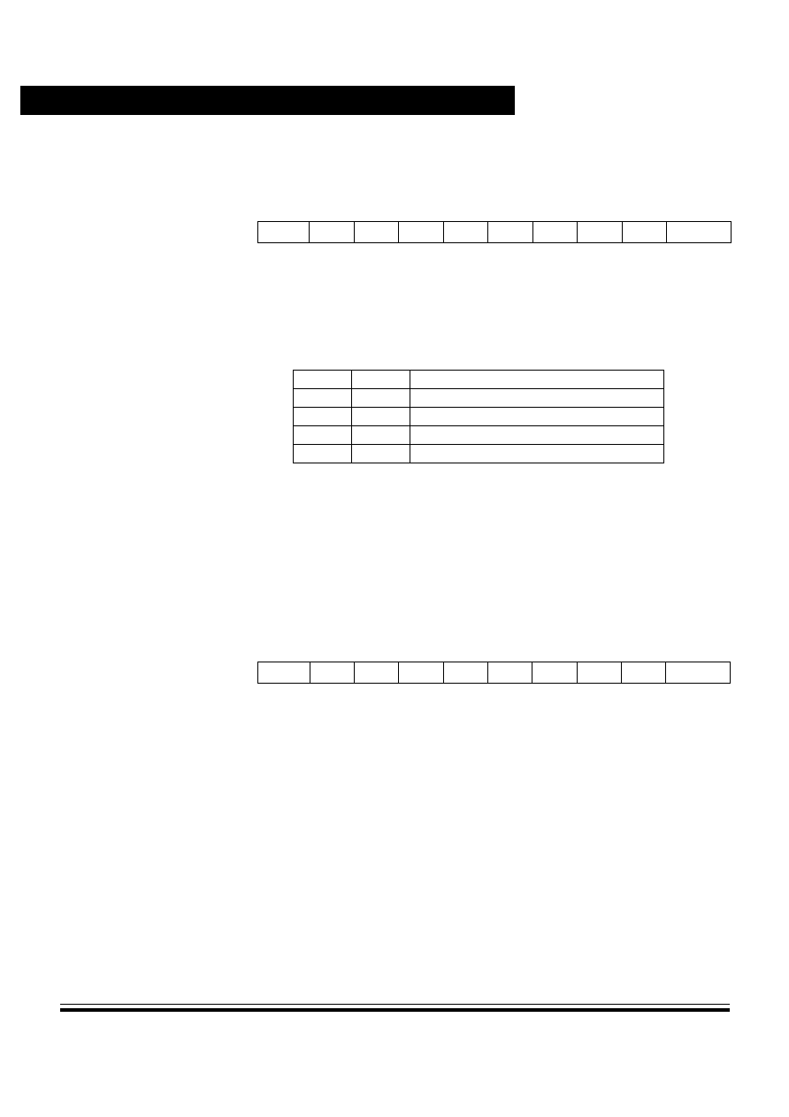
Timing System
Technical Data
MC68HC11P2 -- Rev 1.0
150
Timing System
MOTOROLA
8.5.6 TCTL1 -- Timer control register 1
The bits of this register specify the action taken as a result of a
successful OCx compare.
OM[2:5] -- Output mode
OL[2:5] -- Output level
These control bit pairs are encoded to specify the action taken after a
successful OCx compare. OC5 functions only if the I4/O5 bit in the
PACTL register is clear.
8.5.7 TMSK1 -- Timer interrupt mask register 1
Use this 8-bit register to enable or inhibit the timer input capture and
output compare interrupts.
NOTE:
Bits in TMSK1 correspond bit for bit with flag bits in TFLG1. Ones in
TMSK1 enable the corresponding interrupt sources.
OC1I≠OC4I -- Output compare x interrupt enable
1 = OCx interrupt is enabled.
0 = OCx interrupt is disabled.
If the OCxI enable bit is set when the OCxF flag bit is set, a hardware
interrupt sequence is requested.
Address bit 7
bit 6
bit 5
bit 4
bit 3
bit 2
bit 1
bit 0
State
on reset
Timer control 1 (TCTL1)
$0020
OM2
OL2
OM3
OL3
OM4
OL4
OM5
OL5 0000 0000
OMx
OLx
Action taken on successful compare
0
0
Timer disconnected from OCx pin logic
0
1
Toggle OCx output line
1
0
Clear OCx output line to 0
1
1
Set OCx output line to 1
Address bit 7
bit 6
bit 5
bit 4
bit 3
bit 2
bit 1
bit 0
State
on reset
Timer interrupt mask 1 (TMSK1) $0022
OC1I
OC2I
OC3I
OC4I I4/O5I
IC1I
IC2I
IC3I 0000 0000

Timing System
Output compare
MC68HC11P2 -- Rev 1.0
Technical Data
MOTOROLA
Timing System
151
I4/O5I -- Input capture 4/output compare 5 interrupt enable
1 = IC4/OC5 interrupt is enabled.
0 = IC4/OC5 interrupt is disabled.
When I4/O5 in PACTL is set, I4/O5I is the input capture 4 interrupt
enable bit.
When I4/O5 in PACTL is zero, I4/O5I is the output compare 5 interrupt
enable bit.
IC1I≠IC3I -- Input capture x interrupt enable
1 = ICx interrupt is enabled.
0 = ICx interrupt is disabled.
If the ICxI enable bit is set when the ICxF flag bit is set, a hardware
interrupt sequence is requested.
8.5.8 TFLG1 -- Timer interrupt flag register 1
Bits in this register indicate when timer system events have occurred.
Coupled with the bits of TMSK1, the bits of TFLG1 allow the timer
subsystem to operate in either a polled or interrupt driven system. Clear
flags by writing a one to the corresponding bit position(s).
NOTE:
Bits in TFLG1 correspond bit for bit with flag bits in TMSK1. Ones in
TMSK1 enable the corresponding interrupt sources.
OC1F≠OC4F -- Output compare x flag
1 = Counter has reached the preset output compare x value.
0 = Counter has not reached the preset output compare x value.
These flags are set each time the counter matches the corresponding
output compare x values.
I4/O5F -- Input capture 4/output compare 5 flag
Set by IC4 or OC5, depending on the function enabled by I4/O5 bit in
PACTL
Address bit 7
bit 6
bit 5
bit 4
bit 3
bit 2
bit 1
bit 0
State
on reset
Timer interrupt flag 1 (TFLG1)
$0023 OC1F OC2F OC3F OC4F I4/O5F IC1F
IC2F
IC3F 0000 0000
Timing System
Technical Data
MC68HC11P2 -- Rev 1.0
152
Timing System
MOTOROLA
IC1F≠IC3F -- Input capture x flag
1 = Selected edge has been detected on corresponding port pin.
0 = Selected edge has not been detected on corresponding port
pin.
These flags are set each time a selected active edge is detected on
the ICx input line
8.5.9 TMSK2 -- Timer interrupt mask register 2
Use this 8-bit register to enable or inhibit timer overflow and real-time
interrupts. The timer prescaler control bits are included in this register.
NOTE:
Bits in TMSK2 correspond bit for bit with flag bits in TFLG2. Ones in
TMSK2 enable the corresponding interrupt sources.
TOI -- Timer overflow interrupt enable
1 = Timer overflow interrupt requested when TOF is set.
0 = TOF interrupts disabled.
RTII -- Real-time interrupt enable (refer to
Real-time interrupt
)
PAOVI -- Pulse accumulator overflow interrupt enable (refer to
Pulse accumulator status and interrupt bits
)
PAII -- Pulse accumulator input edge interrupt enable (refer to
Pulse accumulator status and interrupt bits
)
PR[1:0] -- Timer prescaler select
Address
bit 7
bit 6
bit 5
bit 4
bit 3
bit 2
bit 1
bit 0
State
on reset
Timer interrupt mask 2 (TMSK2)
$0024
TOI
RTII
PAOVI
PAII
0
0
PR1
PR0
0000 0000
PR[1:0]
Prescaler
0 0
1
0 1
4
1 0
8
1 1
16

Timing System
Output compare
MC68HC11P2 -- Rev 1.0
Technical Data
MOTOROLA
Timing System
153
These bits are used to select the prescaler divide-by ratio. In normal
modes, PR[1:0] can only be written once, and the write must be within
64 cycles after reset. See
Table 8-1
for specific timing values.
8.5.10 TFLG2 -- Timer interrupt flag register 2
Bits in this register indicate when certain timer system events have
occurred. Coupled with the four high-order bits of TMSK2, the bits of
TFLG2 allow the timer subsystem to operate in either a polled or
interrupt driven system. Clear flags by writing a one to the corresponding
bit position(s).
NOTE:
Bits in TFLG2 correspond bit for bit with flag bits in TMSK2. Ones in
TMSK2 enable the corresponding interrupt sources.
TOF -- Timer overflow interrupt flag
1 = TCNT has overflowed from $FFFF to $0000.
0 = No timer overflow has occurred.
RTIF -- Real time (periodic) interrupt flag (refer to
Real-time interrupt
)
PAOVF -- Pulse accumulator overflow interrupt flag (refer to
Pulse
accumulator
)
PAIF -- Pulse accumulator input edge interrupt flag (refer to
Pulse
accumulator
.)
Bits [3:0] -- Not implemented; always read zero
Address bit 7
bit 6
bit 5
bit 4
bit 3
bit 2
bit 1
bit 0
State
on reset
Timer interrupt flag 2 (TFLG2)
$0025
TOF
RTIF PAOVF PAIF
0
0
0
0
0000 0000

Timing System
Technical Data
MC68HC11P2 -- Rev 1.0
154
Timing System
MOTOROLA
8.6 Real-time interrupt
The real-time interrupt (RTI) feature, used to generate hardware
interrupts at a fixed periodic rate, is controlled and configured by two bits
(RTR1 and RTR0) in the pulse accumulator control (PACTL) register.
The RTII bit in the TMSK2 register enables the interrupt capability. The
four different rates available are a product of the MCU oscillator
frequency and the value of bits RTR[1:0]. Refer to
Table 8-2
, which
shows the periodic real-time interrupt rates.
The clock source for the RTI function is a free-running clock that cannot
be stopped or interrupted except by reset. This clock causes the time
between successive RTI timeouts to be a constant that is independent
of the software latency associated with flag clearing and service. For this
reason, an RTI period starts from the previous timeout, not from when
RTIF is cleared.
Every timeout causes the RTIF bit in TFLG2 to be set, and if RTII is set,
an interrupt request is generated. After reset, one entire RTI period
elapses before the RTIF flag is set for the first time. Refer to the TMSK2,
TFLG2, and PACTL registers.
Table 8-2. RTI periodic rates
RTR[1:0]
E = 3 MHz
E = 2 MHz
E = 1 MHz
E = x MHz
0 0
0 1
1 0
1 1
2.731ms
5.461ms
10.923 ms
21.845 ms
4.096ms
8.192ms
16.384 ms
32.768 ms
8.192ms
16.384 ms
32.768 ms
65.536 ms
2
13
/E
2
14
/E
2
15
/E
2
16
/E

Timing System
Real-time interrupt
MC68HC11P2 -- Rev 1.0
Technical Data
MOTOROLA
Timing System
155
8.6.1 TMSK2 -- Timer interrupt mask register 2
This register contains the real-time interrupt enable bit.
NOTE:
Bits in TMSK2 correspond bit for bit with flag bits in TFLG2. Ones in
TMSK2 enable the corresponding interrupt sources.
TOI -- Timer overflow interrupt enable (refer to
TMSK2 -- Timer
interrupt mask register 2
)
RTII -- Real-time interrupt enable
1 = Real time interrupt requested when RTIF is set.
0 = Real time interrupts disabled.
PAOVI -- Pulse accumulator overflow interrupt enable (refer to
Pulse
accumulator
)
PAII -- Pulse accumulator input edge (refer to
Pulse accumulator
)
PR[1:0] -- Timer prescaler select (refer to
TMSK2 -- Timer interrupt
mask register 2
)
Address bit 7
bit 6
bit 5
bit 4
bit 3
bit 2
bit 1
bit 0
State
on reset
Timer interrupt mask 2 (TMSK2)
$0024
TOI
RTII
PAOVI
PAII
0
0
PR1
PR0 0000 0000

Timing System
Technical Data
MC68HC11P2 -- Rev 1.0
156
Timing System
MOTOROLA
8.6.2 TFLG2 -- Timer interrupt flag register 2
Bits of this register indicate the occurrence of timer system events.
Coupled with the four high-order bits of TMSK2, the bits of TFLG2 allow
the timer subsystem to operate in either a polled or interrupt driven
system. Clear flags by writing a one to the corresponding bit position(s).
NOTE:
Bits in TFLG2 correspond bit for bit with flag bits in TMSK2. Ones in
TMSK2 enable the corresponding interrupt sources.
TOF -- Timer overflow interrupt flag
1 = The timer has overflowed, from $FFFF to $0000.
0 = No timer overflow has occurred.
RTIF -- Real-time interrupt flag
1 = RTI period has elapsed.
0 = RTI flag has been cleared.
The RTIF status bit is automatically set to one at the end of every RTI
period.
PAOVF -- Pulse accumulator overflow interrupt flag (refer to
Pulse
accumulator
)
PAIF -- Pulse accumulator input edge interrupt flag (refer to
Pulse
accumulator
)
Bits [3:0] -- Not implemented; always read zero
Address bit 7
bit 6
bit 5
bit 4
bit 3
bit 2
bit 1
bit 0
State
on reset
Timer interrupt flag 2 (TFLG2)
$0025
TOF
RTIF PAOVF PAIF
0
0
0
0
0000 0000

Timing System
Computer operating properly watchdog function
MC68HC11P2 -- Rev 1.0
Technical Data
MOTOROLA
Timing System
157
8.6.3 PACTL -- Pulse accumulator control register
Bits RTR[1:0] of this register select the rate for the RTI system. The
remaining bits control the pulse accumulator and IC4/OC5 functions.
Bits 7, 3 -- Not implemented; always read zero
PAEN -- Pulse accumulator system enable (refer to
Pulse
accumulator
)
PAMOD -- Pulse accumulator mode (refer to
Pulse accumulator
)
PEDGE -- Pulse accumulator edge control (refer to
Pulse
accumulator
)
I4/O5 -- Input capture 4/output compare (refer to
Pulse
accumulator
)
RTR[1:0] -- RTI interrupt rate select
These two bits determine the rate at which the RTI system requests
interrupts. The RTI system is driven by an E/2
13
clock rate that is
compensated so it is independent of the timer prescaler. These two
control bits select an additional division factor. Refer to
Table 8-2
.
8.7 Computer operating properly watchdog function
The clocking chain for the COP function, tapped off from the main timer
divider chain, is only superficially related to the main timer system. The
CR[1:0] bits in the OPTION register and the NOCOP bit in the CONFIG
register determine the status of the COP function. One additional
register, COPRST, is used to arm and clear the COP watchdog reset
system. Refer to
Resets and Interrupts
for a more detailed discussion
of the COP function.
Address bit 7
bit 6
bit 5
bit 4
bit 3
bit 2
bit 1
bit 0
State
on reset
Pulse accumulator control
(PACTL)
$0026
0
PAEN PAMODPEDGE
0
I4/O5 RTR1 RTR0 0000 0000
Timing System
Technical Data
MC68HC11P2 -- Rev 1.0
158
Timing System
MOTOROLA
8.8 Pulse accumulator
The MC68HC11P2 has an 8-bit counter that can be configured to
operate either as a simple event counter, or for gated time accumulation,
depending on the state of the PAMOD bit in the PACTL register. Refer
to the pulse accumulator block diagram,
Figure 8-3
.
In the event counting mode, the 8-bit counter is clocked to increasing
values by an external pin. The maximum clocking rate for the external
event counting mode is the E clock divided by two. In gated time
accumulation mode, a free-running E clock ˜ 64 signal drives the 8-bit
counter, but only while the external PAI pin is activated. Refer to
Table
8-3
. The pulse accumulator counter can be read or written at any time.
Table 8-3. Pulse accumulator timing
Crystal
frequency
E clock
Cycle
time
64/E
PACNT
overflow
4.0 MHz
1.0 MHz
1000 ns
64 µs
16.384 ms
8.0 MHz
2.0 MHz
500 ns
32 µs
8.192 ms
12.0 MHz
3.0 MHz
333 ns
21.33 µs
5.461 ms
16.0 MHz
4.0 MHz
250 ns
16.0 µs
4.096 ms

Timing System
Pulse accumulator
MC68HC11P2 -- Rev 1.0
Technical Data
MOTOROLA
Timing System
159
Pulse accumulator control bits are also located within two timer
registers, TMSK2 and TFLG2, as described in the following paragraphs.
Figure 8-3. Pulse accumulator block diagram
TOF
0
PAOVF
PAIF
0
0
0
TF
LG2
RTIF
TOI
RTII
0
PAII
0
PR1
PR0
TM
S
K
2
0
PA
E
N
0
PA
M
O
D
PACTL
PAOVI
RT
R
1
RT
R
0
PEDGE
I4
/O
5
&
&
PACNT
1
2
PA7/
OC1/
PAI
2:1
MUX
Input buffer
and edge detector
Output buffer
&
From
DDRA7
From
OC1
E/64 clock
(from main timer)
Overflow
Enable
Clock
Interrupt
requests
Internal data bus
D
i
s
a
b
l
e f
l
ag
se
t
t
i
n
g
Timing System
Technical Data
MC68HC11P2 -- Rev 1.0
160
Timing System
MOTOROLA
8.8.1 PACTL -- Pulse accumulator control register
Four of this register's bits control an 8-bit pulse accumulator system.
Another bit enables either the OC5 function or the IC4 function, while two
other bits select the rate for the real-time interrupt system.
Bits [7, 3] -- Not implemented; always read zero
PAEN -- Pulse accumulator system enable
1 = Pulse accumulator enabled.
0 = Pulse accumulator disabled.
PAMOD -- Pulse accumulator mode
1 = Gated time accumulation mode.
0 = Event counter mode.
PEDGE -- Pulse accumulator edge control
This bit has different meanings depending on the state of the PAMOD
bit, as shown:
I4/O5 -- Input capture 4/output compare 5
1 = Input capture 4 function is enabled (no OC5).
0 = Output compare 5 function is enabled (no IC4).
RTR[1:0] -- RTI interrupt rate selects (refer to
Real-time interrupt
)
Address bit 7
bit 6
bit 5
bit 4
bit 3
bit 2
bit 1
bit 0
State
on reset
Pulse accumulator control
(PACTL)
$0026
0
PAEN PAMODPEDGE
0
I4/O5 RTR1 RTR0 0000 0000
PAMOD
PEDGE
Action of clock
0
0
PAI falling edge increments the counter.
0
1
PAI rising edge increments the counter.
1
0
A zero on PAI inhibits counting.
1
1
A one on PAI inhibits counting.

Timing System
Pulse accumulator
MC68HC11P2 -- Rev 1.0
Technical Data
MOTOROLA
Timing System
161
8.8.2 PACNT -- Pulse accumulator count register
This 8-bit read/write register contains the count of external input events
at the PAI input, or the accumulated count. In gated time accumulation
mode, PACNT is readable even if PAI is not active. The counter is not
affected by reset and can be read or written at any time. Counting is
synchronized to the internal PH2 clock so that incrementing and reading
occur during opposite half cycles.
8.8.3 Pulse accumulator status and interrupt bits
The pulse accumulator control bits, PAOVI and PAII, PAOVF, and PAIF
are located within timer registers TMSK2 and TFLG2.
8.8.3.1 TMSK2 -- Timer interrupt mask 2 register
8.8.3.2 TFLG2 -- Timer interrupt flag 2 register
PAOVI and PAOVF -- Pulse accumulator interrupt enable and overflow
flag
The PAOVF status bit is set each time the pulse accumulator count
rolls over from $FF to $00. To clear this status bit, write a one in the
corresponding data bit position (bit 5) of the TFLG2 register. The
PAOVI control bit allows configuring the pulse accumulator overflow
for polled or interrupt-driven operation and does not affect the state of
PAOVF. When PAOVI is zero, pulse accumulator overflow interrupts
Address bit 7
bit 6
bit 5
bit 4
bit 3
bit 2
bit 1
bit 0
State
on reset
Pulse accumulator count
(PACNT)
$0027
(bit 7)
(6)
(5)
(4)
(3)
(2)
(1)
(bit 0) undefined
Address bit 7
bit 6
bit 5
bit 4
bit 3
bit 2
bit 1
bit 0
State
on reset
Timer interrupt mask 2 (TMSK2)
$0024
TOI
RTII
PAOVI
PAII
0
0
PR1
PR0 0000 0000
Address bit 7
bit 6
bit 5
bit 4
bit 3
bit 2
bit 1
bit 0
State
on reset
Timer interrupt flag 2 (TFLG2)
$0025
TOF
RTIF PAOVF PAIF
0
0
0
0
0000 0000

Timing System
Technical Data
MC68HC11P2 -- Rev 1.0
162
Timing System
MOTOROLA
are inhibited, and the system operates in a polled mode, which
requires that PAOVF be polled by user software to determine when
an overflow has occurred. When the PAOVI control bit is set, a
hardware interrupt request is generated each time PAOVF is set.
Before leaving the interrupt service routine, software must clear
PAOVF by writing to the TFLG2 register.
PAII and PAIF -- Pulse accumulator input edge interrupt enable and flag
The PAIF status bit is automatically set each time a selected edge is
detected at the PA7/PAI/OC1 pin. To clear this status bit, write to the
TFLG2 register with a one in the corresponding data bit position (bit
4). The PAII control bit allows configuring the pulse accumulator input
edge detect for polled or interrupt-driven operation but does not affect
setting or clearing the PAIF bit. When PAII is zero, pulse accumulator
input interrupts are inhibited, and the system operates in a polled
mode. In this mode, the PAIF bit must be polled by user software to
determine when an edge has occurred. When the PAII control bit is
set, a hardware interrupt request is generated each time PAIF is set.
Before leaving the interrupt service routine, software must clear PAIF
by writing to the TFLG register.
8.9 Pulse-width modulation (PWM) timer
The PWM timer subsystem provides up to four 8-bit pulse-width
modulated waveforms on the port H pins. Channel pairs can be
concatenated to create 16-bit PWM outputs. Three clock sources (A, B,
and S) and a flexible clock select scheme give the PWM a wide range of
frequencies.
Four control registers configure the PWM outputs -- PWCLK, PWPOL,
PWSCAL, and PWEN. The PWCLK register selects the prescale value
Pin
Alternate
function
PH0
PW1
PH1
PW2
PH2
PW3
PH3
PW4

Timing System
Pulse-width modulation (PWM) timer
MC68HC11P2 -- Rev 1.0
Technical Data
MOTOROLA
Timing System
163
for the PWM clock sources and enables the 16-bit PWM functions. The
PWPOL register determines each channel's polarity and selects the
clock source for each channel. The PWSCAL register derives a user-
scaled clock based on the A clock source, and the PWEN register
enables the PWM channels.
Each channel also has a separate 8-bit counter, period register, and duty
cycle register. The period and duty cycle registers are double buffered
so that if they are changed while the channel is enabled, the change
does not take effect until the counter rolls over or the channel is disabled.
A new period or duty cycle can be forced into effect immediately by
writing to the period or duty cycle register and then writing to the counter.
With PWMs configured for 8-bit mode and E equal to 4MHz, PWM
signals can be produced from 40 kHz (1% duty cycle resolution) to less
than 10 cycles per second (approximately 0.4% duty cycle resolution).
By configuring the PWMs for 16-bit mode with E equal to 4MHz, PWM
periods greater than one minute are possible.
In 16-bit mode, duty cycle resolution of up to 15 parts per million can be
achieved (at a PWM frequency of 60Hz). In the same system, a PWM
frequency of 1kHz corresponds to a duty cycle resolution of 0.025%.
8.9.1 PWM timer block diagram
Figure 8-4
shows the block diagram of the PWM timer subsystem.
Three different clock sources are selectable and provide inputs to the
control registers. Each of the four channels has a counter, a period
register, and a duty register. The waveform output is the result of a
match between the period register (PWPERx) and the value in the
counter (PWCNTx). The duty register (PWDTYx) changes the state of
the output during the period to determine the duty cycle.

Timing System
Technical Data
MC68HC11P2 -- Rev 1.0
164
Timing System
MOTOROLA
Figure 8-4. PWM timer block diagram
MCU
E clock
8-bit comparator
EQ
PWSCAL
Div
i
de
r
Prescale select
˜
1, 2, 4, 8, 16, 32, 64, 128
Prescale select
˜
1, 2, 4, 8
PCKB1 PCKB2 PCKB3
PCKA2
PCKA1
8-bit counter
˜
2
Clock
select
Clock
select
PWEN3
PWEN4
CON34
Clock B
Clock A
Cl
ock
S
CON12
PWEN1
PWEN2
PCLK4
PCLK3
PCLK2
PCLK1
reset
4
8
8-bit comparator
EQ
PH0/
PW1
PWDTY1
Bit 0
Bit 1
Bit 2
Bit 3
S
Q
Q
R
MUX
8-bit comparator
EQ
PWPER1
8-bit comparator
EQ
PWDTY2
8-bit comparator
EQ
PWPER2
carry
S
Q
Q
R
MUX
16-bit
PWM
control
reset
reset
PPOL2
PPOL1
CON12
8-bit comparator
EQ
PWDTY3
S
Q
Q
R
MUX
8-bit comparator
EQ
PWPER3
8-bit comparator
EQ
PWDTY4
8-bit comparator
EQ
PWPER4
carry
S
Q
Q
R
MUX
16-bit
PWM
control
reset
reset
PPOL4
PPOL3
CON34
Port H
pin
control
PH1/
PW2
PH2/
PW3
PH3/
PW4
PW
CNT3
PW
CNT4
P
W
CNT2
PW
CN
T
1
CNT1
CNT2
CNT3
CNT4

Timing System
Pulse-width modulation (PWM) timer
MC68HC11P2 -- Rev 1.0
Technical Data
MOTOROLA
Timing System
165
8.9.2 PWCLK -- PWM clock prescaler and 16-bit select register
This register contains bits for selecting the 16-bit PWM options and for
selecting the prescaler values for the clocks.
8.9.2.1 16-bit PWM function
The PWCLK register contains two control bits, each of which is used to
concatenate a pair of PWM channels into one 16-bit channel. Channels
3 and 4 are concatenated with the CON34 bit, and channels 1 and 2 are
concatenated with the CON12 bit.
When the 16-bit concatenated mode is selected, the clock source is
determined by the low order channel. Channel 2 is the low order channel
when channels 1 and 2 are concatenated. Channel 4 is the low order
channel when channels 3 and 4 are concatenated. The pins associated
with channels 1 and 3 can be used for general-purpose I/O when 16-bit
PWM mode is selected.
Channel 1 registers are the high order byte of the double-byte channel
when channels 1 and 2 are concatenated. Channel 3 registers are the
high order byte of the double-byte channel when channels 3 and 4 are
concatenated. Reads of the high order byte cause the low order byte to
be latched for one cycle to guarantee that double byte reads are
accurate. Writes to the low byte of the counter cause reset of the entire
counter. Writes to the upper bytes of the counter have no effect.
CON34 -- Concatenate channels 3 and 4
1 = Channels 3 and 4 are concatenated into one 16-bit PWM
channel.
0 = Channels 3 and 4 are separate 8-bit PWMs.
When concatenated, channel 3 is the high-order byte and the channel
4 pin (PH3) is the output.
Address bit 7
bit 6
bit 5
bit 4
bit 3
bit 2
bit 1
bit 0
State
on reset
Pulse width clock select (PWCLK) $0060 CON34CON12PCKA2PCKA1
0
PCKB3 PCKB2PCKB1 0000 0000

Timing System
Technical Data
MC68HC11P2 -- Rev 1.0
166
Timing System
MOTOROLA
CON12 -- Concatenate Channels 1 and 2
1 = Channels 1 and 2 are concatenated into one 16-bit PWM
channel.
0 = Channels 1 and 2 are separate 8-bit PWMs.
When concatenated, channel 1 is the high-order byte and the channel
2 pin (PH1) is the output.
8.9.2.2 Clock prescaler selection
The three available clocks are clock A, clock B, and clock S (scaled).
Clock A can be software selected to be E, E/2, E/4, or E/8. Clock B can
be software selected to be E, E/2, E/4,..., E/128. The scaled clock (clock
S) uses clock A as an input and divides it with a reloadable counter. The
rates available are software selectable to be clock A/2, down to clock A
/512.
The clock source portion of the block diagram shows the three clock
sources and how the scaled clock is created. Clock A is an input to an 8-
bit counter which is then compared to a user programmable scale value.
When they match, this circuit has an output that is divided by two and the
counter is reset.
Each PWM timer channel can be driven by one of two clocks. Refer to
Figure 8-4
.
PCKA[2:1] -- Prescaler for clock A
Determines the frequency of clock A. Refer to
Table 8-4
.
Bit 3 -- Not implemented; always reads zero
PCKB[3:1] -- Prescaler for clock B
Determines the frequency of clock B. Refer to
Table 8-4
.

Timing System
Pulse-width modulation (PWM) timer
MC68HC11P2 -- Rev 1.0
Technical Data
MOTOROLA
Timing System
167
8.9.3 PWPOL -- PWM timer polarity & clock source select register
PCLK[4:3] -- Pulse width channel 4/3 clock select
1 = Clock S is source.
0 = Clock B is source.
PCLK[2:1] -- Pulse width channel 2/1 clock select
1 = Clock S is source.
0 = Clock A is source.
PPOL[4:1] -- Pulse width channel x polarity
1 = PWM channel x output is high at the beginning of the clock
cycle and goes low when duty count is reached.
0 = PWM channel x output is low at the beginning of the clock cycle
and goes high when duty count is reached.
Each channel has a polarity bit that allows a cycle to start with either
a high or a low level. This is shown on the block diagram,
Figure 8-4
,
as a selection of either the Q output or the Q output of the PWM output
flip flop. When one of the bits in the PWPOL register is set, the
associated PWM channel output is high at the beginning of the clock
cycle, then goes low when the duty count is reached.
Table 8-4. Clock A and clock B prescalers
PCKA[2:1]
Clock A
PCKB[3:1]
Clock B
0 0
E
0 0 0
E
0 1
E/2
0 0 1
E/2
1 0
E/4
0 1 0
E/4
1 1
E/8
0 1 1
E/8
1 0 0
E/16
1 0 1
E/32
1 1 0
E/64
1 1 1
E/128
Address bit 7
bit 6
bit 5
bit 4
bit 3
bit 2
bit 1
bit 0
State
on reset
Pulse width polarity select
(PWPOL)
$0061 PCLK4 PCLK3 PCLK2 PCLK1 PPOL4 PPOL3 PPOL2 PPOL1 0000 0000

Timing System
Technical Data
MC68HC11P2 -- Rev 1.0
168
Timing System
MOTOROLA
8.9.4 PWSCAL -- PWM timer prescaler register
Scaled clock S is generated by dividing clock A by the value in PWSCAL,
then dividing the result by two. If PWSCAL = $00, clock A is divided by
256, then divided by two to generate clock S.
8.9.5 PWEN -- PWM timer enable register
Each timer has an enable bit to start its waveform output. Writing any of
these PWENx bits to one causes the associated port line to become an
output regardless of the state of the associated DDR bit. This does not
change the state of the DDR bit and when PWENx returns to zero the
DDR bit again controls I/O state. On the front end of the PWM timer the
clock is connected to the PWM circuit by the PWENx enable bit being
high. There is a synchronizing circuit to guarantee that the clock will only
be enabled or disabled at an edge.
PWEN contains 4 PWM enable bits -- one for each channel. When an
enable bit is set to one, the pulse modulated signal becomes available
at the associated port pin.
TPWSL -- PWM scaled clock test bit (Test mode only)
1 = Clock S output to PWSCAL register (Test only).
0 = Normal operation.
When TPWSL is one, clock S from the PWM timer is output to
PWSCAL register. Normal writing to the PWSCAL register still
functions.
DISCP -- Disable compare scaled E clock (Test mode only)
1 = Match of period does not reset associated count register (Test
only).
0 = Normal operation.
Address bit 7
bit 6
bit 5
bit 4
bit 3
bit 2
bit 1
bit 0
State
on reset
Pulse width scale (PWSCAL)
$0062
(bit 7)
(6)
(5)
(4)
(3)
(2)
(1)
(bit 0) 0000 0000
Address bit 7
bit 6
bit 5
bit 4
bit 3
bit 2
bit 1
bit 0
State
on reset
Pulse width enable (PWEN)
$0063 TPWSL DISCP
0
0
PWEN4PWEN3PWEN2PWEN10000 0000

Timing System
Pulse-width modulation (PWM) timer
MC68HC11P2 -- Rev 1.0
Technical Data
MOTOROLA
Timing System
169
Bits [5:4] -- Not implemented; always read zero
PWEN[4:1] -- Pulse width channels 4≠1
1 = Channel enabled on the associated port pin.
0 = Channel disabled.
8.9.6 PWCNT1≠4 -- PWM timer counter registers 1 to 4
Each channel has its own counter which can be read at any time without
affecting the count or the operation of the PWM channel. Writing to a
counter causes it to be reset to $00; this is generally done before the
counter is enabled. A counter may also be written to whilst it is enabled;
this may cause a truncated PWM period.
8.9.7 PWPER1≠4 -- PWM timer period registers 1 to 4
There is one period register for each channel. The value in this register
determines the period of the associated PWM timer channel. PWPERx
is connected internally to a buffer which compares directly with the
counter register. The period value in PWPERx is loaded into the buffer
when the counter is cleared by the termination of the previous period or
by a write to the counter. This register can be written at any time, and the
written value will take effect from the start of the next PWM timer cycle.
Reads of this register return the most recent value written.
Address bit 7
bit 6
bit 5
bit 4
bit 3
bit 2
bit 1
bit 0
State
on reset
Pulse width count 1 (PWCNT1)
$0064
(bit 7)
(6)
(5)
(4)
(3)
(2)
(1)
(bit 0) 0000 0000
Pulse width count 2 (PWCNT2)
$0065
(bit 7)
(6)
(5)
(4)
(3)
(2)
(1)
(bit 0) 0000 0000
Pulse width count 3 (PWCNT3)
$0066
(bit 7)
(6)
(5)
(4)
(3)
(2)
(1)
(bit 0) 0000 0000
Pulse width count 4 (PWCNT4)
$0067
(bit 7)
(6)
(5)
(4)
(3)
(2)
(1)
(bit 0) 0000 0000
Address bit 7
bit 6
bit 5
bit 4
bit 3
bit 2
bit 1
bit 0
State
on reset
Pulse width period 1 (PWPER1)
$0068
(bit 7)
(6)
(5)
(4)
(3)
(2)
(1)
(bit 0) 1111 1111
Pulse width period 2 (PWPER2)
$0069
(bit 7)
(6)
(5)
(4)
(3)
(2)
(1)
(bit 0) 1111 1111
Pulse width period 3 (PWPER3) $006A (bit 7)
(6)
(5)
(4)
(3)
(2)
(1)
(bit 0) 1111 1111
Pulse width period 4 (PWPER4) $006B (bit 7)
(6)
(5)
(4)
(3)
(2)
(1)
(bit 0) 1111 1111
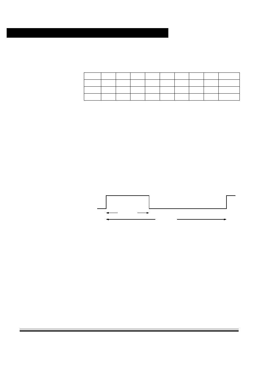
Timing System
Technical Data
MC68HC11P2 -- Rev 1.0
170
Timing System
MOTOROLA
8.9.8 PWDTY1≠4 -- PWM timer duty cycle registers 1 to 4
There is one duty register for each channel. The value in this register
determines the duty cycle of the associated PWM timer channel.
PWDTYx is compared to the counter contents and if they are equal, a
match occurs and the output goes to the state defined by the associated
polarity bit. If the register is written while the channel is enabled, then the
new value is held in a buffer until the counter rolls over or the channel is
disabled. Reads of this register return the most recent value written.
NOTE:
If PWDTYx S PWPERx then there will be no change of state due to the
duty cycle value. In addition, if the duty register is set to $00, then the
output will always be in the state which would normally be result from the
duty change of state (see also
Boundary cases
).
Address bit 7
bit 6
bit 5
bit 4
bit 3
bit 2
bit 1
bit 0
State
on reset
Pulse width duty 1 (PWDTY1)
$006C (bit 7)
(6)
(5)
(4)
(3)
(2)
(1)
(bit 0) 1111 1111
Pulse width duty 2 (PWDTY2)
$006D (bit 7)
(6)
(5)
(4)
(3)
(2)
(1)
(bit 0) 1111 1111
Pulse width duty 3 (PWDTY3)
$006E
(bit 7)
(6)
(5)
(4)
(3)
(2)
(1)
(bit 0) 1111 1111
Pulse width duty 4 (PWDTY4)
$006F
(bit 7)
(6)
(5)
(4)
(3)
(2)
(1)
(bit 0) 1111 1111
Figure 8-5. PWM duty cycle
PWMx
PWPERx
PWDTYx

Timing System
Pulse-width modulation (PWM) timer
MC68HC11P2 -- Rev 1.0
Technical Data
MOTOROLA
Timing System
171
8.9.9 Boundary cases
The following boundary conditions apply to the values stored in the
PWDTYx and PWPERx registers and the PPOLx bits:
∑
If PWDTYx = $00, PWPERx > $00 and PPOLx = 0 then the output
is always high.
∑
If PWDTYx = $00, PWPERx > $00 and PPOLx = 1 then the output
is always low.
∑
If PWDTYx S PWPERx and PPOLx = 0 then the output is always
low.
∑
If PWDTYx S PWPERx and PPOLx = 1 then the output is always
high.
∑
If PWPERx = $00 and PPOLx = 0 then the output is always low.
∑
If PWPERx = $00 and PPOLx = 1 then the output is always high.

Timing System
Technical Data
MC68HC11P2 -- Rev 1.0
172
Timing System
MOTOROLA

MC68HC11P2 -- Rev 1.0
Technical Data
MOTOROLA
Analog-to-Digital Converter
173
Technical Data -- MC68HC11P2
Section 9. Analog-to-Digital Converter
9.1 Contents
9.2
Introduction. . . . . . . . . . . . . . . . . . . . . . . . . . . . . . . . . . . . . . 173
9.3
Overview . . . . . . . . . . . . . . . . . . . . . . . . . . . . . . . . . . . . . . . .174
9.4
A/D converter power-up and clock select . . . . . . . . . . . . . 178
9.5
Channel assignments. . . . . . . . . . . . . . . . . . . . . . . . . . . . . . 180
9.6
Control, status and results registers . . . . . . . . . . . . . . . . . 181
9.7
Operation in STOP and WAIT modes . . . . . . . . . . . . . . . . . 184
9.2 Introduction
The analog-to-digital (A/D) system, a successive approximation
converter, uses an all-capacitive charge redistribution technique to
convert analog signals to digital values.
The A/D converter shares input pins with port E:
Pin
Alternate
function
PE0
AD0
PE1
AD1
PE2
AD2
PE3
AD3
PE4
AD4
PE5
AD5
PE6
AD6
PE7
AD7
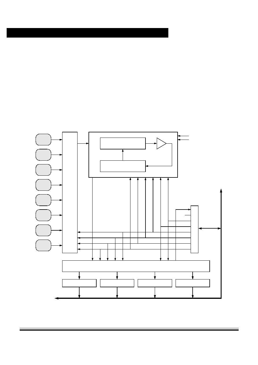
Analog-to-Digital Converter
Technical Data
MC68HC11P2 -- Rev 1.0
174
Analog-to-Digital Converter
MOTOROLA
9.3 Overview
The A/D system is an 8-channel, 8-bit, multiplexed-input converter. The
VDD AD and VSS AD pins are used to input supply voltage to the A/D
converter. This allows the supply voltage to be bypassed independently.
The converter does not require external sample and hold circuits
because of the type of charge redistribution technique used. A/D
converter timing can be synchronized to the system E clock, or to an
internal resistor capacitor (RC) oscillator. The A/D converter system
consists of four functional blocks: multiplexer, analog converter, digital
control and result storage. Refer to
Figure 9-1
.
Figure 9-1. A/D converter block diagram
PE0/
AD0
PE1/
AD1
PE2/
AD2
PE3/
AD3
PE4/
AD4
PE5/
AD5
PE6/
AD6
PE7/
AD7
CCF
0
SCAN
MULT
CD
CC
CB
CA
AD
CT
L
≠
A/
D
c
o
n
t
ro
l
Analog
MUX
Result register interface
ADR1 - A/D result 1
ADR2 - A/D result 2
ADR3 - A/D result 3
ADR4 - A/D result 4
Successive approximation
register and control
8-bit capacitive DAC
with sample and hold
VRH
VRL
Result
Internal
data bus

Analog-to-Digital Converter
Overview
MC68HC11P2 -- Rev 1.0
Technical Data
MOTOROLA
Analog-to-Digital Converter
175
9.3.1 Multiplexer
The multiplexer selects one of 16 inputs for conversion. Input selection
is controlled by the value of bits CD ≠ CA in the ADCTL register. The
eight port E pins are fixed-direction analog inputs to the multiplexer, and
additional internal analog signal lines are routed to it.
Port E pins can also be used as digital inputs. Digital reads of port E pins
are not recommended during the sample portion of an A/D conversion
cycle, when the gate signal to the N-channel input gate is on. Because
no P-channel devices are directly connected to either input pins or
reference voltage pins, voltages above V
DD
do not cause a latchup
problem, although current should be limited according to maximum
ratings. Refer to
Figure 9-2
, which is a functional diagram of an input
pin.
Figure 9-2. Electrical model of an A/D input pin (in sample mode)
4kæ
<2pF
V
RL
Analog
input
400nA
junction
leakage
Diffusion and
poly coupler
20pF
DAC
capacitance
Note 1: The analog switch is closed only during the 12 cycle sample time
Note 1
Input
protection
device
+20V
≠0.7V
Note 2: All component values are approximate

Analog-to-Digital Converter
Technical Data
MC68HC11P2 -- Rev 1.0
176
Analog-to-Digital Converter
MOTOROLA
9.3.2 Analog converter
Conversion of an analog input selected by the multiplexer occurs in this
block. It contains a digital-to-analog capacitor (DAC) array, a
comparator, and a successive approximation register (SAR). Each
conversion is a sequence of eight comparison operations, beginning
with the most significant bit (MSB). Each comparison determines the
value of a bit in the SAR.
The DAC array performs two functions. It acts as a sample and hold
circuit during the entire conversion sequence, and provides comparison
voltage to the comparator during each successive comparison.
The result of each successive comparison is stored in the SAR. When a
conversion sequence is complete, the contents of the SAR are
transferred to the appropriate result register.
A charge pump provides switching voltage to the gates of analog
switches in the multiplexer. Charge pump output must stabilize between
7 and 8 volts within up to 100 µs before the converter can be used. The
charge pump is enabled by the ADPU bit in the OPTION register.
9.3.3 Digital control
All A/D converter operations are controlled by bits in register ADCTL. In
addition to selecting the analog input to be converted, ADCTL bits
indicate conversion status, and control whether single or continuous
conversions are performed. Finally, the ADCTL bits determine whether
conversions are performed on single or multiple channels.
9.3.4 Result registers
Four 8-bit registers (ADR1 ≠ ADR4) store conversion results. Each of
these registers can be accessed by the processor in the CPU. The
conversion complete flag (CCF) indicates when valid data is present in
the result registers. The result registers are written during a portion of the
system clock cycle when reads do not occur, so there is no conflict.
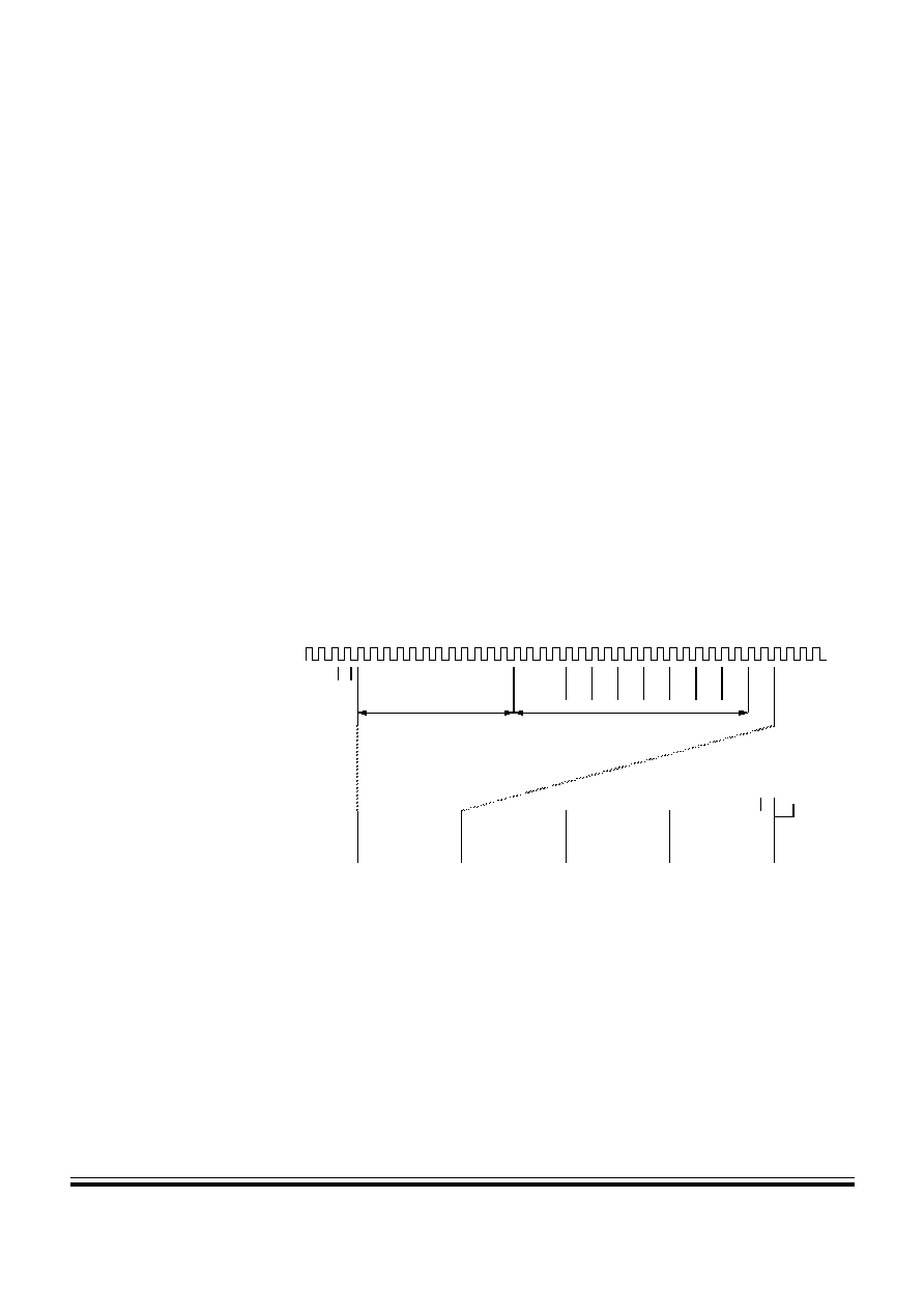
Analog-to-Digital Converter
Overview
MC68HC11P2 -- Rev 1.0
Technical Data
MOTOROLA
Analog-to-Digital Converter
177
9.3.5 A/D converter clocks
The CSEL bit in the OPTION register selects whether the A/D converter
uses the system E clock or an internal RC oscillator for synchronization.
When E clock frequency is below 750kHz, charge leakage in the
capacitor array can cause errors, and the internal oscillator should be
used. When the RC clock is used, additional errors can occur because
the comparator is sensitive to the additional system clock noise.
9.3.6 Conversion sequence
A/D converter operations are performed in sequences of four
conversions each. A conversion sequence can repeat continuously or
stop after one iteration. The conversion complete flag (CCF) is set after
the fourth conversion in a sequence to show the availability of data in the
result registers.
Figure 9-3
shows the timing of a typical sequence.
Synchronization is referenced to the system E clock.
9.3.7 Conversion process
The A/D conversion sequence begins one E clock cycle after a write to
the A/D control/status register, ADCTL. The bits in ADCTL select the
channel and the mode of conversion.
Figure 9-3. A/D conversion sequence
E clock
Sample analog input
Successive approximation sequence
12 cycles
4 cycles
2 cyc 2 cyc 2 cyc 2 cyc 2 cyc 2 cyc 2 cyc 2 cyc
MSB
bit 6 bit 5 bit 4 bit 3 bit 2 bit 1 bit 0
END
W
r
it
e t
o
A
DCT
L
Convert first
channel and
update ADR1
Convert second
channel and
update ADR2
Convert third
channel and
update ADR3
Convert fourth
channel and
update ADR4
S
e
t C
C
F
fl
a
g
Repeat
sequence
if
S
C
A
N
=
1
0
32
64
96
128 E clock cycles

Analog-to-Digital Converter
Technical Data
MC68HC11P2 -- Rev 1.0
178
Analog-to-Digital Converter
MOTOROLA
An input voltage equal to V
RL
converts to $00 and an input voltage equal
to V
RH
converts to $FF (full scale), with no overflow indication. For
ratiometric conversions of this type, the source of each analog input
should use V
RH
as the supply voltage and be referenced to V
RL
.
9.4 A/D converter power-up and clock select
ADPU (bit 7 of the OPTION register) controls A/D converter power up.
Clearing ADPU removes power from and disables the A/D converter
system; setting ADPU enables the A/D converter system. After the A/D
converter is turned on, the analog bias voltages will take up to 100µs to
stabilize.
When the A/D converter system is operating from the MCU E clock, all
switching and comparator operations are synchronized to the MCU
clocks. This allows the comparator results to be sampled at `quiet' times,
which minimizes noise errors. The internal RC oscillator is asynchronous
with respect to the MCU clock, so noise can affect the A/D converter
results. This results in a slightly lower typical accuracy when using the
internal oscillator (CSEL = 1).
9.4.1 OPTION -- System configuration options register 1
The 8-bit special-purpose OPTION register sets internal system
configuration options during initialization. The time protected control bits,
IRQE, DLY, FCME and CR[1:0] can be written to only once in the first 64
cycles after a reset and then they become read-only bits. This minimizes
the possibility of any accidental changes to the system configuration.
They may be written at any time in special modes.
ADPU -- A/D power-up
1 = A/D system power enabled.
0 = A/D system disabled, to reduce supply current.
Address bit 7
bit 6
bit 5
bit 4
bit 3
bit 2
bit 1
bit 0
State
on reset
System config. options 1
(OPTION)
$0039 ADPU CSEL IRQE
DLY
CME FCME
CR1
CR0 0001 0000

Analog-to-Digital Converter
A/D converter power-up and clock select
MC68HC11P2 -- Rev 1.0
Technical Data
MOTOROLA
Analog-to-Digital Converter
179
After enabling the A/D power, at least 100µs should be allowed for
system stabilization.
CSEL -- Clock select
1 = A/D and EEPROM use internal RC clock source (about
1.5MHz).
0 = A/D and EEPROM use system E clock (must be at least 1MHz).
Selects alternate clock source for on-chip EEPROM and A/D charge
pumps. The on-chip RC clock should be used when the E clock
frequency falls below 1MHz.
IRQE -- Configure IRQ for falling edge sensitive operation (refer to
Operating Modes and On-Chip Memory
)
1 = Falling edge sensitive operation.
0 = Low level sensitive operation.
DLY -- Enable oscillator start-up delay
1 = A delay of approximately 4000 E clock cycles is imposed as the
MCU is started up from the STOP mode.
0 = The oscillator start-up delay coming out of STOP is bypassed
and the MCU resumes processing within about four bus
cycles. A stable external oscillator is required if this option is
selected.
CME -- Clock monitor enable (refer to
Resets and Interrupts
)
1 = Clock monitor enabled.
0 = Clock monitor disabled.
FCME -- Force clock monitor enable (refer to
Resets and Interrupts
)
1 = Clock monitor enabled, cannot be disabled until next reset.
0 = Clock monitor follows the state of the CME bit.
CR[1:0] -- COP timer rate select bits (refer to
Resets and Interrupts
)

Analog-to-Digital Converter
Technical Data
MC68HC11P2 -- Rev 1.0
180
Analog-to-Digital Converter
MOTOROLA
9.5 Channel assignments
The multiplexer allows the A/D converter to select one of sixteen analog
signals. Eight of these channels correspond to port E input lines to the
MCU, four others are internal reference points or test functions; the
remaining four channels are reserved. Refer to
Table 9-1
.
9.5.1 Single-channel operation
There are two types of single-channel operation. In the first type (SCAN
= 0), the single selected channel is converted four consecutive times.
The first result is stored in A/D result register 1 (ADR1), and the fourth
result is stored in ADR4. After the fourth conversion is complete, all
conversion activity is halted until a new conversion command is written
to the ADCTL register. In the second type of single-channel operation
(SCAN = 1), conversions continue to be performed on the selected
channel with the fifth conversion being stored in register ADR1
(overwriting the first conversion result), the sixth conversion overwriting
ADR2, and so on.
Table 9-1. A/D converter channel assignments
Channel
number
Channel
signal
Result in ADRx
if MULT = 1
1
AN0
ADR1
2
AN1
ADR2
3
AN2
ADR3
4
AN3
ADR4
5
AN4
ADR1
6
AN5
ADR2
7
AN6
ADR3
8
AN7
ADR4
9≠12
reserved
--
13
V
RH
(1)
1. Used for factory testing.
ADR1
14
V
RL
*
ADR2
15
V
RH
/2
*
ADR3
16
reserved
*
ADR4

Analog-to-Digital Converter
Control, status and results registers
MC68HC11P2 -- Rev 1.0
Technical Data
MOTOROLA
Analog-to-Digital Converter
181
9.5.2 Multiple-channel operation
There are two types of multiple-channel operation. In the first type
(SCAN = 0), a selected group of four channels is converted once only.
The first result is stored in A/D result register 1 (ADR1), and the fourth
result is stored in ADR4. After the fourth conversion is complete, all
conversion activity is halted until a new conversion command is written
to the ADCTL register. In the second type of multiple-channel operation
(SCAN = 1), conversions continue to be performed on the selected
group of channels with the fifth conversion being stored in register ADR1
(replacing the earlier conversion result for the first channel in the group),
the sixth conversion overwriting ADR2, and so on.
9.6 Control, status and results registers
9.6.1 ADCTL -- A/D control and status register
All bits in this register can be read or written, except bit 7, which is a read-
only status indicator, and bit 6, which always reads as zero. Write to
ADCTL to initiate a conversion. To quit a conversion in progress, write to
this register and a new conversion sequence begins immediately.
CCF -- Conversions complete flag
1 = All four A/D result registers contain valid conversion data.
0 = At least one of the A/D result registers contains invalid data.
A read-only status indicator, this bit is set when all four A/D result
registers contain valid conversion results. Each time the ADCTL
register is overwritten, this bit is automatically cleared to zero and a
conversion sequence is started. In the continuous mode, CCF is set
at the end of the first conversion sequence.
Bit 6 -- Not implemented; always reads zero.
Address bit 7
bit 6
bit 5
bit 4
bit 3
bit 2
bit 1
bit 0
State
on reset
A/D control & status (ADCTL)
$0030
CCF
0
SCAN MULT
CD
CC
CB
CA
u0uu uuuu

Analog-to-Digital Converter
Technical Data
MC68HC11P2 -- Rev 1.0
182
Analog-to-Digital Converter
MOTOROLA
SCAN -- Continuous scan control
1 = A/D conversions take place continuously.
0 = Each of the four conversions is performed only once.
When this control bit is clear, the four requested conversions are
performed once to fill the four result registers. When this control bit is
set, conversions continue in a round-robin fashion with the result
registers updated as data becomes available.
MULT -- Multiple-channel/single-channel control
1 = Each A/D channel has a result register allocated to it.
0 = Four consecutive conversions from the same A/D channel are
stored in the results registers.
When this bit is clear, the A/D converter system is configured to
perform four consecutive conversions on the single channel specified
by the four channel select bits CD≠CA (bits 3≠0 of the ADCTL
register). When this bit is set, the A/D system is configured to perform
a conversion on each of four channels where each result register
corresponds to one channel.
NOTE:
When the multiple-channel continuous scan mode is used, extra care is
needed in the design of circuitry driving the A/D inputs. The charge on
the capacitive DAC array before the sample time is related to the voltage
on the previously converted channel. A charge share situation exists
between the internal DAC capacitance and the external circuit
capacitance. Although the amount of charge involved is small, the rate
at which it is repeated is every 64 µs for an E clock of 2 MHz. The RC
charging rate of the external circuit must be balanced against this charge
sharing effect to avoid errors in accuracy. Refer to the M68HC11
Reference Manual (M68HC11RM/AD) for further information.
CD≠CA -- Channel selects D≠A
When a multiple channel mode is selected (MULT = 1), the two least
significant channel select bits (CB and CA) have no meaning and the
CD and CC bits specify which group of four channels is to be
converted.

Analog-to-Digital Converter
Control, status and results registers
MC68HC11P2 -- Rev 1.0
Technical Data
MOTOROLA
Analog-to-Digital Converter
183
9.6.2 ADR1≠ADR4 -- A/D converter results registers
These read-only registers hold an 8-bit conversion result. Writes to these
registers have no effect. Data in the A/D converter result registers is valid
when the CCF flag in the ADCTL register is set, indicating a conversion
sequence is complete. If conversion results are needed sooner, refer to
Figure 9-3
, which shows the A/D conversion sequence diagram.
Channel select
control bits
Channel
signal
Result in ADRx
if MULT = 1
CD:CC:CB:CA
0 0 0 0
AN0
ADR1
0 0 0 1
AN1
ADR2
0 0 1 0
AN2
ADR3
0 0 1 1
AN3
ADR4
0 1 0 0
AN4
ADR1
0 1 0 1
AN5
ADR2
0 1 1 0
AN6
ADR3
0 1 1 1
AN7
ADR4
1 0 X X
reserved
--
1 1 0 0
V
RH
(1)
ADR1
1 1 0 1
V
RL
(1)
ADR2
1 1 1 0
V
RH
/2
(1)
ADR3
1 1 1 1
reserved
(1)
ADR4
1. Used for factory testing.
Address bit 7
bit 6
bit 5
bit 4
bit 3
bit 2
bit 1
bit 0
State
on reset
A/D result 1 (ADR1)
$0031
(bit 7)
(6)
(5)
(4)
(3)
(2)
(1)
(bit 0) undefined
A/D result 2 (ADR2)
$0032
(bit 7)
(6)
(5)
(4)
(3)
(2)
(1)
(bit 0) undefined
A/D result 3 (ADR3)
$0033
(bit 7)
(6)
(5)
(4)
(3)
(2)
(1)
(bit 0) undefined
A/D result 4 (ADR4)
$0034
(bit 7)
(6)
(5)
(4)
(3)
(2)
(1)
(bit 0) undefined

Analog-to-Digital Converter
Technical Data
MC68HC11P2 -- Rev 1.0
184
Analog-to-Digital Converter
MOTOROLA
9.7 Operation in STOP and WAIT modes
If a conversion sequence is in progress when either the STOP or WAIT
mode is entered, the conversion of the current channel is suspended.
When the MCU resumes normal operation, that channel is resampled
and the conversion sequence is resumed. As the MCU exits the WAIT
mode, the A/D circuits are stable and valid results can be obtained on
the first conversion. However, in STOP mode, all analog bias currents
are disabled and it is necessary to allow a stabilization period when
leaving the STOP mode. If the STOP mode is exited with a delay
(DLY = 1), there is enough time for these circuits to stabilize before the
first conversion. If the STOP mode is exited with no delay (DLY bit in
OPTION register = 0), allow 10 ms for the A/D circuitry to stabilize to
avoid invalid results.

MC68HC11P2 -- Rev 1.0
Technical Data
MOTOROLA
Resets and Interrupts
185
Technical Data -- MC68HC11P2
Section 10. Resets and Interrupts
10.1 Contents
10.2
Introduction. . . . . . . . . . . . . . . . . . . . . . . . . . . . . . . . . . . . . . 185
10.3
Resets . . . . . . . . . . . . . . . . . . . . . . . . . . . . . . . . . . . . . . . . . . 185
10.4
Effects of reset . . . . . . . . . . . . . . . . . . . . . . . . . . . . . . . . . . . 192
10.5
Reset and interrupt priority . . . . . . . . . . . . . . . . . . . . . . . . . 195
10.6
Interrupts . . . . . . . . . . . . . . . . . . . . . . . . . . . . . . . . . . . . . . . . 200
10.7
Low power operation . . . . . . . . . . . . . . . . . . . . . . . . . . . . . . 203
10.2 Introduction
Resets and interrupt operations load the program counter with a vector
that points to a new location from which instructions are to be fetched. A
reset immediately stops execution of the current instruction and forces
the program counter to a known starting address. Internal registers and
control bits are initialized so that the MCU can resume executing
instructions. An interrupt temporarily suspends normal program
execution whilst an interrupt service routine is being executed. After an
interrupt has been serviced, the main program resumes as if there had
been no interruption.
10.3 Resets
There are four possible sources of reset. Power-on reset (POR) and
external reset share the normal reset vector. The computer operating
properly (COP) reset and the clock monitor reset each has its own
vector.

Resets and Interrupts
Technical Data
MC68HC11P2 -- Rev 1.0
186
Resets and Interrupts
MOTOROLA
10.3.1 Power-on reset
A positive transition on VDD generates a power-on reset (POR), which
is used only for power-up conditions. POR cannot be used to detect
drops in power supply voltages. A 4064 t
CYC
(internal clock cycle) delay
after the oscillator becomes active allows the clock generator to
stabilize. If RESET is at logical zero at the end of 4064 t
CYC
, the CPU
remains in the reset condition until RESET goes to logical one.
It is important to protect the MCU during power transitions. Most
M68HC11 systems need an external circuit that holds the RESET pin
low whenever V
DD
is below the minimum operating level. This external
voltage level detector, or other external reset circuits, are the usual
source of reset in a system. The POR circuit only initializes internal
circuitry during cold starts. Refer to
Figure 2-2
.
10.3.2 External reset (RESET)
The CPU distinguishes between internal and external reset conditions
by sensing whether the reset pin rises to a logic one in less than two E
clock cycles after an internal device releases reset. When a reset
condition is sensed, the RESET pin is driven low by an internal device
for four E clock cycles, then released. Two E clock cycles later it is
sampled. If the pin is still held low, the CPU assumes that an external
reset has occurred. If the pin is high, it indicates that the reset was
initiated internally by either the COP system or the clock monitor. It is not
advisable to connect an external resistor capacitor (RC) power-up delay
circuit to the reset pin of M68HC11 devices because the circuit charge
time constant can cause the device to misinterpret the type of reset that
occurred.
10.3.3 COP reset
The MCU includes a COP system to help protect against software
failures. When the COP is enabled, the software is responsible for
keeping a free-running watchdog timer from timing out. When the
software is no longer being executed in the intended sequence, a
system reset is initiated.

Resets and Interrupts
Resets
MC68HC11P2 -- Rev 1.0
Technical Data
MOTOROLA
Resets and Interrupts
187
The state of the NOCOP bit in the CONFIG register determines whether
the COP system is enabled or disabled. To change the enable status of
the COP system, change the contents of the CONFIG register and then
perform a system reset. In the special test and bootstrap operating
modes, the COP system is initially inhibited by the disable resets (DISR)
control bit in the TEST1 register. The DISR bit can subsequently be
written to zero to enable COP resets.
The COP timer rate control bits CR[1:0] in the OPTION register
determine the COP timeout period. The system E clock is divided by 2
15
and then further scaled by a factor shown in
Table 10-1
. After reset,
these bits are zero, which selects the shortest timeout period. In normal
operating modes, these bits can only be written once within 64 bus
cycles after reset.
10.3.4 COPRST -- Arm/reset COP timer circuitry register
Complete the following reset sequence to service the COP timer. Write
$55 to COPRST to arm the COP timer clearing mechanism. Then write
$AA to COPRST to clear the COP timer. Executing instructions between
Table 10-1. COP timer rate select
CR[1:0]
Divide
E/2
15
by
XTAL = 8 MHz:
timeout
(1)
1. The timeout period has a tolerance of ≠0/+one cycle of the E/2
15
clock due to the
asynchronous implementation of the COP circuitry. For example, with XTAL = 8MHz,
the uncertainty is ≠0/+16.384ms. See also the M68HC11 Reference Manual,
(M68HC11RM/AD).
XTAL = 12MHz:
timeout
(1)
XTAL = 16MHz:
timeout
(1)
0 0
1
16.384 ms
10.923 ms
8.192 ms
0 1
4
65.536 ms
43.691 ms
32.768 ms
1 0
16
262.14 ms
174.76 ms
131.07 ms
1 1
64
1.049 sec
699.05 ms
524.29 ms
E =
2.0 MHz
3.0 MHz
4.0 MHz
Address bit 7
bit 6
bit 5
bit 4
bit 3
bit 2
bit 1
bit 0
State
on reset
COP timer arm/reset (COPRST) $003A (bit 7)
(6)
(5)
(4)
(3)
(2)
(1)
(bit 0)
not
affected

Resets and Interrupts
Technical Data
MC68HC11P2 -- Rev 1.0
188
Resets and Interrupts
MOTOROLA
these two steps is possible as long as both steps are completed in the
correct sequence before the timer times out.
10.3.5 Clock monitor reset
The clock monitor circuit is based on an internal RC time delay. If no
MCU clock edges are detected within this RC time delay, the clock
monitor can optionally generate a system reset. The clock monitor
function is enabled or disabled by the CME control bit in the OPTION
register. The presence of a timeout is determined by the RC delay, which
allows the clock monitor to operate without any MCU clocks.
Clock monitor is used as a backup for the COP system. Because the
COP needs a clock to function, it is disabled when the clocks stop.
Therefore, the clock monitor system can detect clock failures not
detected by the COP system.
Semiconductor wafer processing causes variations of the RC timeout
values between individual devices. An E clock frequency below 10 kHz
is detected as a clock monitor error. An E clock frequency of 200 kHz or
more prevents clock monitor errors. Using the clock monitor function
when the E clock is below 200 kHz is not recommended.
Special considerations are needed when a STOP instruction is executed
and the clock monitor is enabled. Because the STOP function causes
the clocks to be halted, the clock monitor function generates a reset
sequence if it is enabled at the time the STOP mode was initiated. Before
executing a STOP instruction, clear the CME bit in the OPTION register
to zero to disable the clock monitor. After recovery from STOP, set the
CME bit to logic one to enable the clock monitor.

Resets and Interrupts
Resets
MC68HC11P2 -- Rev 1.0
Technical Data
MOTOROLA
Resets and Interrupts
189
10.3.6 OPTION -- System configuration options register 1
The special-purpose OPTION register sets internal system configuration
options during initialization. The time protected control bits (IRQE, DLY,
FCME and CR[1:0]) can be written to only once in the first 64 cycles after
a reset and then they become read-only bits. This minimizes the
possibility of any accidental changes to the system configuration. They
may be written at any time in special modes.
ADPU -- A/D power-up (Refer to
Analog-to-Digital Converter
)
1 = A/D system power enabled.
0 = A/D system disabled, to reduce supply current.
CSEL -- Clock select (Refer to
Analog-to-Digital Converter
)
1 = A/D and EEPROM use internal RC clock source (about
1.5MHz).
0 = A/D and EEPROM use system E clock (must be at least 1MHz).
IRQE -- Configure IRQ for falling edge sensitive operation (Refer to
Operating Modes and On-Chip Memory
)
1 = Falling edge sensitive operation.
0 = Low level sensitive operation.
DLY -- Enable oscillator start-up delay (Refer to
Operating Modes and
On-Chip Memory
)
1 = A delay of approximately 4000 E clock cycles is imposed as the
MCU is started up from the STOP mode.
0 = The oscillator start-up delay coming out of STOP is bypassed.
CME -- Clock monitor enable
1 = Clock monitor enabled.
0 = Clock monitor disabled.
Address bit 7
bit 6
bit 5
bit 4
bit 3
bit 2
bit 1
bit 0
State
on reset
System config. options 1
(OPTION)
$0039 ADPU CSEL IRQE
DLY
CME FCME
CR1
CR0 0001 0000

Resets and Interrupts
Technical Data
MC68HC11P2 -- Rev 1.0
190
Resets and Interrupts
MOTOROLA
This control bit can be read or written at any time and controls whether
or not the internal clock monitor circuit triggers a reset sequence when
the system clock is slow or absent. When it is clear, the clock monitor
circuit is disabled, and when it is set, the clock monitor circuit is
enabled. Reset clears the CME bit.
In order to use both STOP and clock monitor, the CME bit should be
cleared before executing STOP, then set again after recovering from
STOP.
FCME -- Force clock monitor enable
1 = Clock monitor enabled; cannot be disabled until next reset.
0 = Clock monitor follows the state of the CME bit.
When FCME is set, slow or stopped clocks will cause a clock failure
reset sequence. To utilize STOP mode, FCME should always be
cleared.
CR[1:0] -- COP timer rate select bits
The internal E clock is first divided by 2
15
before it enters the COP
watchdog system. These control bits determine a scaling factor for the
watchdog timer. See
Table 10-1
.
10.3.7 CONFIG -- Configuration control register
CONFIG controls the presence and location of EEPROM in the memory
map and enables the COP watchdog system. A security feature that
protects data in EEPROM and RAM is available on mask programmed
MCUs. Refer to
RAM and EEPROM security
.
CONFIG is made up of EEPROM cells and static working latches. The
operation of the MCU is controlled directly by these latches and not the
EEPROM byte. When programming the CONFIG register, the EEPROM
byte is accessed. When the CONFIG register is read, the static latches
are accessed.
Address bit 7
bit 6
bit 5
bit 4
bit 3
bit 2
bit 1
bit 0
State
on reset
Configuration control (CONFIG)
$003F ROMAD
1
1
PARENNOSECNOCOPROMON EEON x11x xxxx

Resets and Interrupts
Resets
MC68HC11P2 -- Rev 1.0
Technical Data
MOTOROLA
Resets and Interrupts
191
These bits can be read at any time. The value read is the one latched
into the register from the EEPROM cells during the last reset sequence.
A new value programmed into this register is not readable until after a
subsequent reset sequence. Unused bits always read as ones.
If SMOD = 1, CONFIG bits can be written at any time. If SMOD = 0,
CONFIG bits can only be written using the EEPROM programming
sequence, and are neither readable nor active until latched via the next
reset.
ROMAD -- ROM mapping control (refer to
Operating Modes and On-
Chip Memory
)
1 = ROM addressed from $8000 to $FFFF.
0 = ROM addressed from $0000 to $7FFF (expanded mode only).
Bits [6,5] -- Not implemented; always read one
PAREN -- Pull-up assignment register enable (refer to
Parallel
Input/Output
)
1 = PPAR register enabled; pull-ups can be enabled using PPAR.
0 = PPAR register disabled; all pull-ups disabled.
NOSEC -- EEPROM security disabled (refer to
Operating Modes and
On-Chip Memory
)
1 = Disable security.
0 = Enable security.
NOCOP -- COP system disable
1 = COP system disabled.
0 = COP system enabled (forces reset on timeout).
ROMON -- ROM enable (refer to
Operating Modes and On-Chip
Memory
)
1 = ROM included in the memory map.
0 = ROM excluded from the memory map.
EEON -- EEPROM enable (refer to
Operating Modes and On-Chip
Memory
)
1 = EEPROM included in the memory map.
0 = EEPROM excluded from the memory map.
Resets and Interrupts
Technical Data
MC68HC11P2 -- Rev 1.0
192
Resets and Interrupts
MOTOROLA
10.4 Effects of reset
When a reset condition is recognized, the internal registers and control
bits are forced to an initial state. Depending on the cause of the reset and
the operating mode, the reset vector can be fetched from any of six
possible locations, as shown in
Table 10-2
.
These initial states then control on-chip peripheral systems to force them
to known start-up states, as described in the following paragraphs.
10.4.1 Central processing unit
After reset, the CPU fetches the restart vector from the appropriate
address during the first three cycles, and begins executing instructions.
The stack pointer and other CPU registers are indeterminate
immediately after reset; however, the X and I interrupt mask bits in the
condition code register (CCR) are set to mask any interrupt requests.
Also, the S-bit in the CCR is set to inhibit the STOP mode.
10.4.2 Memory map
After reset, the INIT register is initialized to $00, putting the 1024 bytes
of RAM at locations $0080 ≠$047F, and the control registers at locations
$0000≠$007F. The INIT2 register puts EEPROM at locations
$0D80≠$0FFF.
Table 10-2. Reset cause, reset vector and operating mode
Cause of reset
Normal mode vector
Special test or bootstrap
POR or RESET pin
$FFFE, $FFFF
$BFFE, $BFFF
Clock monitor failure
$FFFC, $FFFD
$BFFC, $BFFD
COP watchdog timeout
$FFFA, $FFFB
$BFFA, $BFFB

Resets and Interrupts
Effects of reset
MC68HC11P2 -- Rev 1.0
Technical Data
MOTOROLA
Resets and Interrupts
193
10.4.3 Parallel I/O
When a reset occurs in expanded operating modes, port B, C, and F pins
used for parallel I/O are dedicated to the expansion bus. If a reset occurs
during a single chip operating mode, all ports are configured as general-
purpose high-impedance inputs.
NOTE:
Do not confuse pin function with the electrical state of the pin at reset. All
general-purpose I/O pins configured as inputs at reset are in a high-
impedance state. Port data registers reflect the port's functional state at
reset. The pin function is mode dependent.
10.4.4 Timer
During reset, the timer system is initialized to a count of $0000. The
prescaler bits are cleared, and all output compare registers are initialized
to $FFFF. All input capture registers are indeterminate after reset. The
output compare 1 mask (OC1M) register is cleared so that successful
OC1 compares do not affect any I/O pins. The other four output
compares are configured so that they do not affect any I/O pins on
successful compares. All input capture edge-detector circuits are
configured for capture disabled operation. The timer overflow interrupt
flag and all eight timer function interrupt flags are cleared. All nine timer
interrupts are disabled because their mask bits have been cleared.
The I4/O5 bit in the PACTL register is cleared to configure the I4/O5
function as OC5; however, the OM5:OL5 control bits in the TCTL1
register are clear so OC5 does not control the PA3 pin.
10.4.5 Real-time interrupt (RTI)
The real-time interrupt flag (RTIF) is cleared and automatic hardware
interrupts are masked. The rate control bits are cleared after reset and
can be initialized by software before the real-time interrupt (RTI) system
is used.

Resets and Interrupts
Technical Data
MC68HC11P2 -- Rev 1.0
194
Resets and Interrupts
MOTOROLA
10.4.6 Pulse accumulator
The pulse accumulator system is disabled at reset so that the pulse
accumulator input (PAI) pin defaults to being a general-purpose input
pin.
10.4.7 Computer operating properly (COP)
The COP watchdog system is enabled if the NOCOP control bit in the
CONFIG register is cleared, and disabled if NOCOP is set. The COP rate
is set for the shortest duration timeout.
10.4.8 Serial communications interface (SCI)
The reset condition of the SCI system is independent of the operating
mode. At reset, the SCI baud rate control register is initialized to $0004.
All transmit and receive interrupts are masked and both the transmitter
and receiver are disabled so the port pins default to being general
purpose I/O lines. The SCI frame format is initialized to an 8-bit character
size. The send break and receiver wake-up functions are disabled. The
TDRE and TC status bits in the SCI status register are both set,
indicating that there is no transmit data in either the transmit data register
or the transmit serial shift register. The RDRF, IDLE, OR, NF, FE, PF,
and RAF receive-related status bits are cleared.
NOTE:
The foregoing paragraph also applies to SCI2 and SCI3. Their
respective MI BUS functions are disabled, since MIEx is cleared on
reset.
10.4.9 Serial peripheral interface (SPI)
The SPI system is disabled by reset. The port pins associated with this
function default to being general-purpose I/O lines.

Resets and Interrupts
Reset and interrupt priority
MC68HC11P2 -- Rev 1.0
Technical Data
MOTOROLA
Resets and Interrupts
195
10.4.10 Analog-to-digital converter
The A/D converter configuration is indeterminate after reset. The ADPU
bit is cleared by reset, which disables the A/D system. The conversion
complete flag is cleared by reset.
10.4.11 System
The EEPROM programming controls are disabled, so the memory
system is configured for normal read operation. PSEL[4:0] are initialized
with the binary value %00110, causing the external IRQ pin to have the
highest I-bit interrupt priority. The IRQ pin is configured for level-
sensitive operation (for wired-OR systems). The RBOOT, SMOD, and
MDA bits in the HPRIO register reflect the status of the MODB and
MODA inputs at the rising edge of reset. The DLY control bit is set to
specify that an oscillator start-up delay is imposed upon recovery from
STOP mode. The clock monitor system is disabled because CME and
FCME are cleared.
10.5 Reset and interrupt priority
Resets and interrupts have a hardware priority that determines which
reset or interrupt is serviced first when simultaneous requests occur. Any
maskable interrupt can be given priority over other maskable interrupts.
The first six interrupt sources are not maskable by the I-bit in the CCR.
The priority arrangement for these sources is fixed and is as follows:
1. POR or RESET pin
2. Clock monitor reset
3. COP watchdog reset
4. XIRQ interrupt
≠
Illegal opcode interrupt -- see
Illegal opcode trap
for details
of handling
≠
Software interrupt (SWI) -- see
Software interrupt
for details
of handling

Resets and Interrupts
Technical Data
MC68HC11P2 -- Rev 1.0
196
Resets and Interrupts
MOTOROLA
The maskable interrupt sources have the following priority arrangement:
1. IRQ
2. Real-time interrupt
3. Timer input capture 1
4. Timer input capture 2
5. Timer input capture 3
6. Timer output compare 1
7. Timer output compare 2
8. Timer output compare 3
9. Timer output compare 4
10. Timer input capture 4/output compare 5
11. SCI2/MI BUS system
12. SCI3/MI BUS system
13. Timer overflow
14. Pulse accumulator overflow
15. Pulse accumulator input edge
16. SPI transfer complete
17. SCI1 system
Any one of these maskable interrupts can be assigned the highest
maskable interrupt priority by writing the appropriate value to the PSEL
bits in the HPRIO register. Otherwise, the priority arrangement remains
the same. An interrupt that is assigned highest priority is still subject to
global masking by the I-bit in the CCR, or by any associated local bits.
Interrupt vectors are not affected by priority assignment. To avoid race
conditions, HPRIO can only be written while I-bit interrupts are inhibited.

Resets and Interrupts
Reset and interrupt priority
MC68HC11P2 -- Rev 1.0
Technical Data
MOTOROLA
Resets and Interrupts
197
10.5.1 HPRIO -- Highest priority I-bit interrupt and misc. register
RBOOT, SMOD, and MDA bits depend on power-up initialization mode
and can only be written in special modes when SMOD = 1. Refer to
Table 3-4
.
RBOOT -- Read bootstrap ROM (refer to
Operating Modes and On-
Chip Memory
)
1 = Bootloader ROM enabled, at $BE40≠$BFFF.
0 = Bootloader ROM disabled and not in map.
SMOD -- Special mode select (refer to
Operating Modes and On-Chip
Memory
)
1 = Special mode variation in effect.
0 = Normal mode variation in effect.
MDA -- Mode select A (refer to
Operating Modes and On-Chip
Memory
)
1 = Normal expanded or special test mode in effect.
0 = Normal single chip or special bootstrap mode in effect.
PSEL[4:0] -- Priority select bits
These bits select one interrupt source to be elevated above all other
I-bit-related sources and can be written to only while the I-bit in the
CCR is set (interrupts disabled). See
Table 10-3
.
Address bit 7
bit 6
bit 5
bit 4
bit 3
bit 2
bit 1
bit 0
State
on reset
Highest priority interrupt (HPRIO) $003C
RBOO
T
SMOD MDA PSEL4 PSEL3 PSEL2 PSEL1 PSEL0 xxx0 0110

Resets and Interrupts
Technical Data
MC68HC11P2 -- Rev 1.0
198
Resets and Interrupts
MOTOROLA
Table 10-3. Highest priority interrupt selection
PSELx
Interrupt source promoted
4
3
2
1
0
0
0
0
X
X
reserved (default to IRQ)
0
0
1
0
0
reserved (default to IRQ)
0
0
1
0
1
reserved (default to IRQ)
0
0
1
1
0
IRQ (external pin)
0
0
1
1
1
Real-time interrupt
0
1
0
0
0
Timer input capture 1
0
1
0
0
1
Timer input capture 2
0
1
0
1
0
Timer input capture 3
0
1
0
1
1
Timer output compare 1
0
1
1
0
0
Timer output compare 2
0
1
1
0
1
Timer output compare 3
0
1
1
1
0
Timer output compare 4
0
1
1
1
1
Timer output compare 5/input capture 4
1
0
0
0
0
Timer overflow
1
0
0
0
1
Pulse accumulator overflow
1
0
0
1
0
Pulse accumulator input edge
1
0
0
1
1
SPI serial transfer complete
1
0
1
0
0
SCI1 serial system
1
0
1
0
1
SCI2/MI BUS serial system
1
0
1
1
0
SCI3/MI BUS serial system
1
0
1
1
1
reserved (default to IRQ)
1
1
X
X
X
reserved (default to IRQ)

Resets and Interrupts
Reset and interrupt priority
MC68HC11P2 -- Rev 1.0
Technical Data
MOTOROLA
Resets and Interrupts
199
Table 10-4. Interrupt and reset vector assignments
Vector address
Interrupt source
CCR
mask bit
Local
mask
FFC0, C1 ≠ FFD0, D1 reserved
--
--
FFD2, D3
∑ SCI/MI BUS3 receive data register full
∑ SCI/MI BUS3 receiver overrun
∑ SCI3 transmit data register empty
∑ SCI3 transmit complete
∑ SCI3 idle line detect
I
RIE3
RIE3
TIE3
TCIE3
ILIE3
FFD4, D5
∑ SCI/MI BUS2 receive data register full
∑ SCI/MI BUS2 receiver overrun
∑ SCI2 transmit data register empty
∑ SCI2 transmit complete
∑ SCI2 idle line detect
I
RIE2
RIE2
TIE2
TCIE2
ILIE2
FFD6, D7
∑ SCI1 receive data register full
∑ SCI1 receiver overrun
∑ SCI1 transmit data register empty
∑ SCI1 transmit complete
∑ SCI1 idle line detect
I
RIE
RIE
TIE
TCIE
ILIE
FFD8, D9
SPI serial transfer complete
I
SPIE
FFDA, DB
Pulse accumulator input edge
I
PAII
FFDC, DD
Pulse accumulator overflow
I
PAOVI
FFDE, DF
Timer overflow
I
TOI
FFE0, E1
Timer input capture 4/output compare 5
I
I4/O5I
FFE2, E3
Timer output compare 4
I
OC4I
FFE4, E5
Timer output compare 3
I
OC3I
FFE6, E7
Timer output compare 2
I
OC2I
FFE8, E9
Timer output compare 1
I
OC1I
FFEA, EB
Timer input capture 3
I
IC3I
FFEC, ED
Timer input capture 2
I
IC2I
FFEE, EF
Timer input capture 1
I
IC1I
FFF0, F1
Real-time interrupt
I
RTII
FFF2, F3
IRQ pin
I
None
FFF4, F5
XIRQ pin
X
None
FFF6, F7
Software interrupt
None
None
FFF8, F9
Illegal opcode trap
None
None
FFFA, FB
COP failure
None
NOCOP
FFFC, FD
Clock monitor fail
None
CME
FFFE, FF
RESET
None
None

Resets and Interrupts
Technical Data
MC68HC11P2 -- Rev 1.0
200
Resets and Interrupts
MOTOROLA
10.6 Interrupts
Excluding reset type interrupts, the MC68HC11P2 has 20 interrupt
vectors that support 32 interrupt sources. The 17 maskable interrupts
are generated by on-chip peripheral systems. These interrupts are
recognized when the global interrupt mask bit (I) in the condition code
register (CCR) is clear. The three nonmaskable interrupt sources are
illegal opcode trap, software interrupt, and XIRQ pin. Refer to
Table 10-
4
, which shows the interrupt sources and vector assignments for each
source.
For some interrupt sources, such as the SCI interrupts, the flags are
automatically cleared during the normal course of responding to the
interrupt requests. For example, the RDRF flag in the SCI system is
cleared by the automatic clearing mechanism consisting of a read of the
SCI status register while RDRF is set, followed by a read of the SCI data
register. The normal response to an RDRF interrupt request would be to
read the SCI status register to check for receive errors, then to read the
received data from the SCI data register. These two steps satisfy the
automatic clearing mechanism without requiring any special
instructions.
10.6.1 Interrupt recognition and register stacking
An interrupt can be recognized at any time after it is enabled by its local
mask, if any, and by the global mask bit in the CCR. Once an interrupt
source is recognized, the CPU responds at the completion of the
instruction being executed. Interrupt latency varies according to the
number of cycles required to complete the current instruction. When the
CPU begins to service an interrupt, the contents of the CPU registers are
pushed onto the stack in the order shown in
Table 10-5
. After the CCR
value is stacked, the I-bit and the X-bit, if XIRQ is pending, are set to
inhibit further interrupts. The interrupt vector for the highest priority
pending source is fetched, and execution continues at the address
specified by the vector. At the end of the interrupt service routine, the
return from interrupt instruction is executed and the saved registers are
pulled from the stack in reverse order so that normal program execution
Resets and Interrupts
Interrupts
MC68HC11P2 -- Rev 1.0
Technical Data
MOTOROLA
Resets and Interrupts
201
can resume. Refer to
CPU Core and Instruction Set
for further
information.
10.6.2 Nonmaskable interrupt request (XIRQ)
Nonmaskable interrupts are useful because they can always interrupt
CPU operations. The most common use for such an interrupt is for
serious system problems, such as program runaway or power failure.
The XIRQ input is an updated version of the NMI (nonmaskable
interrupt) input of earlier MCUs.
Upon reset, both the X-bit and I-bit of the CCR are set to inhibit all
maskable interrupts and XIRQ. After minimum system initialization,
software can clear the X-bit by a TAP instruction, enabling XIRQ
interrupts. Thereafter, software cannot set the X-bit. Thus, an XIRQ
interrupt is a nonmaskable interrupt. Because the operation of the I-bit-
related interrupt structure has no effect on the X-bit, the internal XIRQ
pin remains unmasked. In the interrupt priority logic, the XIRQ interrupt
has a higher priority than any source that is maskable by the I-bit. All I-
bit-related interrupts operate normally with their own priority relationship.
When an I-bit-related interrupt occurs, the I-bit is automatically set by
hardware after stacking the CCR byte. The X-bit is not affected. When
an X-bit-related interrupt occurs, both the X and I bits are automatically
set by hardware after stacking the CCR. A return from interrupt
instruction restores the X and I bits to their pre-interrupt request state.
Table 10-5. Stacking order on entry to interrupts
Memory location
CPU registers
SP
PCL
SP ≠ 1
PCH
SP ≠ 2
IYL
SP ≠ 3
IYH
SP ≠ 4
IXL
SP ≠ 5
IXH
SP ≠ 6
ACCA
SP ≠ 7
ACCB
SP ≠ 8
CCR

Resets and Interrupts
Technical Data
MC68HC11P2 -- Rev 1.0
202
Resets and Interrupts
MOTOROLA
10.6.3 Illegal opcode trap
Because not all possible opcodes or opcode sequences are defined, the
MCU includes an illegal opcode detection circuit, which generates an
interrupt request. When an illegal opcode is detected and the interrupt is
recognized, the current value of the program counter is stacked. After
interrupt service is complete, the user should reinitialize the stack pointer
to ensure that repeated execution of illegal opcodes does not cause
stack underflow. Left uninitialized, the illegal opcode vector can point to
a memory location that contains an illegal opcode. This condition causes
an infinite loop that causes stack underflow. The stack grows until the
system crashes.
The illegal opcode trap mechanism works for all unimplemented
opcodes on all four opcode map pages. The address stacked as the
return address for the illegal opcode interrupt is the address of the first
byte of the illegal opcode. Otherwise, it would be almost impossible to
determine whether the illegal opcode had been one or two bytes. The
stacked return address can be used as a pointer to the illegal opcode, so
that the illegal opcode service routine can evaluate the offending
opcode.
10.6.4 Software interrupt
SWI is an instruction, and thus cannot be interrupted until complete. SWI
is not inhibited by the global mask bits in the CCR. Because execution
of SWI sets the I mask bit, once an SWI interrupt begins, other interrupts
are inhibited until SWI is complete, or until user software clears the I bit
in the CCR.
10.6.5 Maskable interrupts
The maskable interrupt structure of the MCU can be extended to include
additional external interrupt sources through the IRQ pin. The default
configuration of this pin is a low-level sensitive wired-OR network. When
an event triggers an interrupt, a software accessible interrupt flag is set.
When enabled, this flag causes a constant request for interrupt service.
After the flag is cleared, the service request is released.

Resets and Interrupts
Low power operation
MC68HC11P2 -- Rev 1.0
Technical Data
MOTOROLA
Resets and Interrupts
203
10.6.6 Reset and interrupt processing
The following flow diagrams illustrate the reset and interrupt process.
Figure 10-1
and
Figure 10-2
illustrate how the CPU begins from a reset
and how interrupt detection relates to normal opcode fetches.
Figure 10-
3
to
Figure 10-4
provide an expanded version of a block in
Figure 10-1
and illustrate interrupt priorities.
Figure 10-6
shows the resolution of
interrupt sources within the SCI subsystem.
10.7 Low power operation
Both STOP and WAIT suspend CPU operation until a reset or interrupt
occurs. The WAIT condition suspends processing and reduces power
consumption to an intermediate level. The STOP condition turns off all
on-chip clocks and reduces power consumption to an absolute minimum
while retaining the contents of all bytes of the RAM.
10.7.1 WAIT
The WAI opcode places the MCU in the WAIT condition, during which
the CPU registers are stacked and CPU processing is suspended until a
qualified interrupt is detected. The interrupt can be an external IRQ, an
XIRQ, or any of the internally generated interrupts, such as the timer or
serial interrupts. The on-chip crystal oscillator remains active throughout
the WAIT stand-by period.
The reduction of power in the WAIT condition depends on how many
internal clock signals driving on-chip peripheral functions can be shut
down. The CPU is always shut down during WAIT. While in the wait
state, the address/data bus repeatedly runs read cycles to the address
where the CCR contents were stacked. The MCU leaves the wait state
when it senses any interrupt that has not been masked.
The free-running timer system is shut down only if the I-bit is set to one
and the COP system is disabled by NOCOP being set to one. Several
other systems can also be in a reduced power consumption state
depending on the state of software-controlled configuration control bits.
Power consumption by the analog-to-digital (A/D) converter is not

Resets and Interrupts
Technical Data
MC68HC11P2 -- Rev 1.0
204
Resets and Interrupts
MOTOROLA
affected significantly by the WAIT condition. However, the A/D converter
current can be eliminated by writing the ADPU bit to zero. The SPI
system is enabled or disabled by the SPE control bit. The SCI transmitter
is enabled or disabled by the TE bit, and the SCI receiver is enabled or
disabled by the RE bit. Therefore the power consumption in WAIT is
dependent on the particular application.
10.7.2 STOP
Executing the STOP instruction while the S-bit in the CCR is equal to
zero places the MCU in the STOP condition. If the S-bit is not zero, the
STOP opcode is treated as a no-op (NOP). The STOP condition offers
minimum power consumption because all clocks, including the crystal
oscillator, are stopped while in this mode. To exit STOP and resume
normal processing, a logic low level must be applied to one of the
external interrupts (IRQ or XIRQ) or to the RESET pin. A pending edge-
triggered IRQ can also bring the CPU out of STOP.
Because all clocks are stopped in this mode, all internal peripheral
functions also stop. The data in the internal RAM is retained as long as
V
DD
power is maintained. The CPU state and I/O pin levels are static and
are unchanged by STOP. Therefore, when an interrupt comes to restart
the system, the MCU resumes processing as if there were no
interruption. If reset is used to restart the system a normal reset
sequence results where all I/O pins and functions are also restored to
their initial states.
To use the IRQ pin as a means of recovering from STOP, the I-bit in the
CCR must be clear (IRQ not masked). The XIRQ pin can be used to
wake up the MCU from STOP regardless of the state of the X-bit in the
CCR, although the recovery sequence depends on the state of the X-bit.
If X is set to zero (XIRQ not masked), the MCU starts up, beginning with
the stacking sequence leading to normal service of the XIRQ request. If
X is set to one (XIRQ masked or inhibited), then processing continues
with the instruction that immediately follows the STOP instruction, and
no XIRQ interrupt service is requested or pending.
Because the oscillator is stopped in STOP mode, a restart delay may be
imposed to allow oscillator stabilization upon leaving STOP. If the

Resets and Interrupts
Low power operation
MC68HC11P2 -- Rev 1.0
Technical Data
MOTOROLA
Resets and Interrupts
205
internal oscillator is being used, this delay is required; however, if a
stable external oscillator is being used, the DLY control bit can be used
to bypass this start-up delay. The DLY control bit is set by reset and can
be optionally cleared during initialization. If the DLY equal to zero option
is used to avoid start-up delay on recovery from STOP, then reset should
not be used as the means of recovering from STOP, as this causes DLY
to be set again by reset, imposing the restart delay. This same delay also
applies to power-on-reset, regardless of the state of the DLY control bit,
but does not apply to a reset while the clocks are running.

Resets and Interrupts
Technical Data
MC68HC11P2 -- Rev 1.0
206
Resets and Interrupts
MOTOROLA
Figure 10-1. Processing flow out of reset (1 of 2)
XIRQ pin
low?
Clock monitor fail
(CME = 1)
COP watchdog
timeout
(NOCOP = 0)
Begin an instruction
sequence
External
reset
Power-on reset
(POR)
Delay
(4064 cycles)
Load program counter
with contents of
$FFFC, $FFFD
(vector fetch)
Load program counter
with contents of
$FFFE, $FFFF
(vector fetch)
Load program counter
with contents of
$FFFA, $FFFB
(vector fetch)
Set S, X, and I bits
in CCR.
Reset MCU hardware
X-bit in
CCR set?
Stack CPU registers.
Set X and I bits.
Fetch vector at
$FFF4, $FFF5
1A
1B
No
No
Yes
Yes
Priority
Highest
Lowest
Resets and Interrupts
Low power operation
MC68HC11P2 -- Rev 1.0
Technical Data
MOTOROLA
Resets and Interrupts
207
Figure 10-2. Processing flow out of reset (2 of 2)
RTI?
Fetch
opcode
SWI?
Stack CPU registers.
Set X and I bits.
Fetch vector at
$FFF8, $FFF9
1B
1A
I-bit in
CCR set?
I-bit interrupt
pending?
Legal
opcode?
WAI?
Execute this
instruction
Yes
No
No
Yes
No
No
No
Stack CPU registers.
Set X and I bits.
Fetch vector at
$FFF6, $FFF7
Restore
CPU registers
from Stack
Yes
Yes
No
Stack
CPU registers
Stack
CPU registers
Interrupt
yet?
Set I-bit
Resolve interrupt
priority and fetch
vector
for highest pending
source (
Figure 10-3
)
Yes
Yes
No
Start next instruction
sequence
Yes
Resets and Interrupts
Technical Data
MC68HC11P2 -- Rev 1.0
208
Resets and Interrupts
MOTOROLA
Figure 10-3. Interrupt priority resolution (1 of 3)
X-bit in
CCR set?
Highest priority
interrupt?
RTII = 1?
IC1I = 1?
IC2I = 1?
IC3I = 1?
OC1I = 1?
Begin
IRQ?
2A
XIRQ pin
low?
Set X-bit in CCR.
Fetch vector at
$FFF4, $FFF5
Fetch vector
Fetch vector at
$FFF2, $FFF3
Fetch vector at
$FFF0, $FFF1
Fetch vector at
$FFEE, $FFEF
Fetch vector at
$FFEC, $FFED
Fetch vector at
$FFEA, $FFEB
No
Yes
Fetch vector at
$FFE8, $FFE9
RTIF = 1?
IC1F = 1?
IC2F = 1?
IC3F = 1?
OC1F = 1?
2B
Yes
Yes
Yes
Yes
Yes
Yes
Yes
No
No
No
No
No
No
No
Yes
Yes
Yes
Yes
Yes
No
No
No
No
No
No
Yes
Resets and Interrupts
Low power operation
MC68HC11P2 -- Rev 1.0
Technical Data
MOTOROLA
Resets and Interrupts
209
Figure 10-4. Interrupt priority resolution (2 of 3)
OC2I = 1?
OC3I = 1?
OC4I = 1?
I4/O5I = 1?
2A
Fetch vector at
$FFE6, $FFE7
Fetch vector at
$FFE4, $FFE5
Fetch vector at
$FFE2, $FFE3
Fetch vector at
$FFE0, $FFE1
OC2F = 1?
OC3F = 1?
OC4F = 1?
I4/O5F = 1?
2B
Yes
Yes
Yes
Yes
No
No
No
No
Yes
Yes
Yes
Yes
No
No
No
No
SCI2
interrupt?
Yes
Refer to
Figure 10-6
for further details on SCI interrupts.
Fetch vector at
$FFD4, $FFD5
SCI3
interrupt?
Yes
Fetch vector at
$FFD2, $FFD3
2C
2D
TOI = 1?
Fetch vector at
$FFDE, $FFDF
TOF = 1?
Yes
No
Yes
No
PAOVI = 1?
Fetch vector at
$FFDC, $FFDD
PAOVF = 1?
Yes
No
Yes
No

Resets and Interrupts
Technical Data
MC68HC11P2 -- Rev 1.0
210
Resets and Interrupts
MOTOROLA
Figure 10-5. Interrupt priority resolution (3 of 3)
2C
PAII = 1?
Fetch vector at
$FFDA, $FFDB
PAIF = 1?
2D
Yes
No
Yes
No
SCI1
interrupt?
SPIE = 1?
Fetch vector at
$FFD8, $FFD9
SPIF = 1?
Yes
No
Yes
No
MODF = 1?
No
No
Yes
Yes
Fetch vector at
$FFF2, $FFF3
Spurious interrupt -- take IRQ vector
END
Refer to
Figure 10-6
for further details on SCI interrupts.
Fetch vector at
$FFD6, $FFD7

Resets and Interrupts
Low power operation
MC68HC11P2 -- Rev 1.0
Technical Data
MOTOROLA
Resets and Interrupts
211
Figure 10-6. Interrupt source resolution within the SCI subsystem
No
Begin
RDRF = 1?
OR = 1?
TDRE = 1?
TC = 1?
IDLE = 1?
No valid SCI
interrupt request
RIE = 1?
TE = 1?
RE = 1?
TIE = 1?
TCIE = 1?
ILIE = 1?
RE = 1?
Valid SCI
interrupt request
Yes
Yes
Yes
Yes
Yes
Yes
Yes
Yes
Yes
Yes
Yes
Yes
No
No
No
No
No
No
No
No
No
No
No
Note:
The bit names shown are for SCI1. The diagram
applies equally to SCI2 and SCI3, when the
appropriate bit names are substituted.

Resets and Interrupts
Technical Data
MC68HC11P2 -- Rev 1.0
212
Resets and Interrupts
MOTOROLA

MC68HC11P2 -- Rev 1.0
Technical Data
MOTOROLA
CPU Core and Instruction Set
213
Technical Data -- MC68HC11P2
Section 11. CPU Core and Instruction Set
11.1 Contents
11.2
Introduction. . . . . . . . . . . . . . . . . . . . . . . . . . . . . . . . . . . . . . 213
11.3
Registers . . . . . . . . . . . . . . . . . . . . . . . . . . . . . . . . . . . . . . . . 214
11.4
Data types . . . . . . . . . . . . . . . . . . . . . . . . . . . . . . . . . . . . . . . 220
11.5
Opcodes and operands . . . . . . . . . . . . . . . . . . . . . . . . . . . . 220
11.6
Addressing modes . . . . . . . . . . . . . . . . . . . . . . . . . . . . . . . . 221
11.7
Instruction set . . . . . . . . . . . . . . . . . . . . . . . . . . . . . . . . . . . .223
11.2 Introduction
This section discusses the M68HC11 central processing unit (CPU)
architecture, its addressing modes and the instruction set. For more
detailed information on the instruction set, refer to the M68HC11
Reference Manual (M68HC11RM/AD).
The CPU is designed to treat all peripheral, I/O and memory locations
identically, as addresses in the 64kbyte memory map. This is referred to
as memory-mapped I/O. There are no special instructions for I/O that are
separate from those used for memory. This architecture also allows
accessing an operand from an external memory location with no
execution-time penalty.
CPU Core and Instruction Set
Technical Data
MC68HC11P2 -- Rev 1.0
214
CPU Core and Instruction Set
MOTOROLA
11.3 Registers
M68HC11 CPU registers are an integral part of the CPU and are not
addressed as if they were memory locations. The seven registers are
shown in
Figure 11-1
and are discussed in the following paragraphs.
11.3.1 Accumulators A, B and D
Accumulators A and B are general-purpose 8-bit registers that hold
operands and results of arithmetic calculations or data manipulations.
For some instructions, these two accumulators are treated as a single
double-byte (16-bit) accumulator called accumulator D. Although most
operations can use accumulators A or B interchangeably, the following
exceptions apply:
∑
The ABX and ABY instructions add the contents of 8-bit
accumulator B to the contents of 16-bit register X or Y, but there
are no equivalent instructions that use A instead of B.
∑
The TAP and TPA instructions transfer data from accumulator A
to the condition code register, or from the condition code register
to accumulator A, however, there are no equivalent instructions
that use B rather than A.
Figure 11-1. Programming model
Accumulator A
7
0
Accumulator B
7
0
Double accumulator D
15
0
Index register X
15
0
Index register Y
15
0
Stack pointer
15
0
Program counter
15
0
S
C
X H
I
N Z V
A:B
D
IX
IY
SP
PC
CCR
Condition code register
Carry
Overflow
Zero
Negative
I interrupt mask
Half carry (from bit 3)
X interrupt mask
Stop disable

CPU Core and Instruction Set
Registers
MC68HC11P2 -- Rev 1.0
Technical Data
MOTOROLA
CPU Core and Instruction Set
215
∑
The decimal adjust accumulator A (DAA) instruction is used after
binary-coded decimal (BCD) arithmetic operations, but there is no
equivalent BCD instruction to adjust accumulator B.
∑
The add, subtract, and compare instructions associated with both
A and B (ABA, SBA, and CBA) only operate in one direction,
making it important to plan ahead to ensure the correct operand is
in the correct accumulator.
11.3.2 Index register X (IX)
The IX register provides a 16-bit indexing value that can be added to the
8-bit offset provided in an instruction to create an effective address. The
IX register can also be used as a counter or as a temporary storage
register.
11.3.3 Index register Y (IY)
The 16-bit IY register performs an indexed mode function similar to that
of the IX register. However, most instructions using the IY register
require an extra byte of machine code and an extra cycle of execution
time because of the way the opcode map is implemented. Refer to
Opcodes and operands
for further information.
11.3.4 Stack pointer (SP)
The M68HC11 CPU has an automatic program stack. This stack can be
located anywhere in the address space and can be any size up to the
amount of memory available in the system. Normally the SP is initialized
by one of the first instructions in an application program. The stack is
configured as a data structure that grows downward from high memory
to low memory. Each time a new byte is pushed onto the stack, the SP
is decremented. Each time a byte is pulled from the stack, the SP is
incremented. At any given time, the SP holds the 16-bit address of the
next free location in the stack.
Figure 11-2
is a summary of SP
operations.
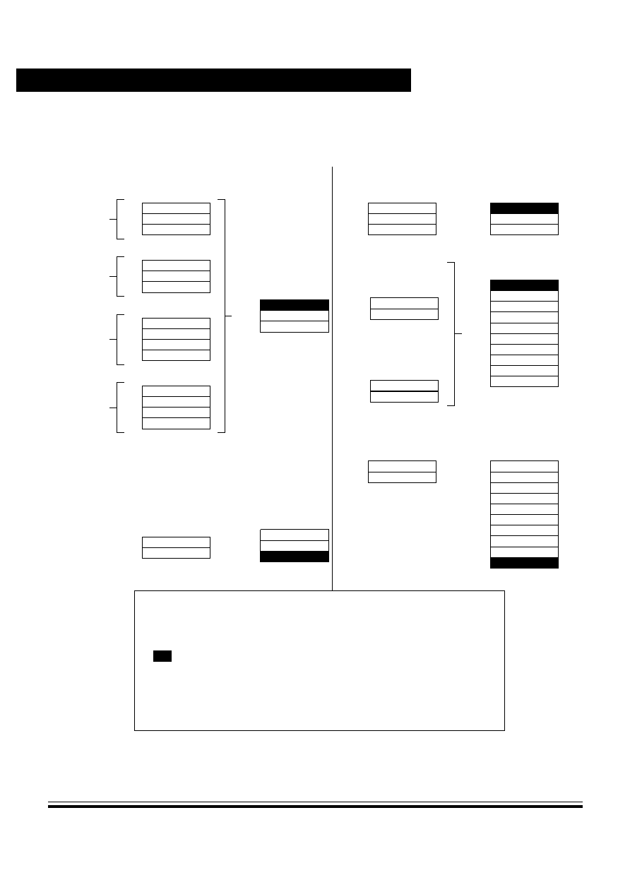
CPU Core and Instruction Set
Technical Data
MC68HC11P2 -- Rev 1.0
216
CPU Core and Instruction Set
MOTOROLA
Figure 11-2. Stacking operations
$9D = JSR
Main program
JSR, Jump to subroutine
PC
DIRECT
dd
ff
Main program
Next instruction
RTN
$AD = JSR
PC
Next instruction
RTN
$18 = PRE
PC
Main program
$AD = JSR
ff
Next instruction
RTN
$BD = JSR
PC
hh
ll
Next instruction
RTN
Main program
$8D = BSR
PC
rr
Main program
Next instruction
RTN
BSR, Branch to subroutine
$39 = RTS
PC
Main program
IND, X
IND, Y
EXTEND
RTN
L
SP
RTN
H
SP≠1
SP≠2
Stack
RTN
L
SP
RTN
H
SP≠1
SP≠2
Stack
RTN
L
SP+2
RTN
H
SP+1
SP
Stack
$3B = RTI
PC
SP
Condition Code
SP+1
RTI, Return from interrupt
Interrupt program
Stack
Accumulator B
SP+2
Accumulator A
SP+3
Index register (IX
H
)
SP+4
Index register (IX
L
)
SP+5
Index register (IY
H
)
SP+6
Index register (IY
L
)
SP+7
RTN
H
SP+8
RTN
L
SP+9
$3F = SWI
PC
RTN
SP≠9
Condition Code
SP≠8
Main program
Stack
Accumulator B
SP≠7
Accumulator A
SP≠6
Index register (IX
H
)
SP≠5
Index register (IX
L
)
SP≠4
Index register (IY
H
)
SP≠3
Index register (IY
L
)
SP≠2
RTN
H
SP≠1
SWI, Software interrupt
RTN
L
SP
WAI, Wait for interrupt
$3E = WAI
PC
RTN
Main program
RTS, Return from subroutine
Legend
RTN
Address of the next instruction in the main program, to be executed on return from subroutine
RTN
H
More significant byte of return address
RTN
L
Less significant byte of return address
Shaded cells show stack pointer position after the operation is complete
dd
8-bit direct address ($0000≠$00FF); the high byte is assumed to be $00
ff
8-bit positive offset ($00 to $FF (0 to 256)) is added to the index register contents
hh
High order byte of 16-bit extended address
ll
Low order byte of 16-bit extended address
rr
Signed relative offset ($80 to $7F (≠128 to +127)); offset is relative to the address following the offset byte

CPU Core and Instruction Set
Registers
MC68HC11P2 -- Rev 1.0
Technical Data
MOTOROLA
CPU Core and Instruction Set
217
When a subroutine is called by a jump to subroutine (JSR) or branch to
subroutine (BSR) instruction, the address of the instruction after the JSR
or BSR is automatically pushed onto the stack, less significant byte first.
When the subroutine is finished, a return from subroutine (RTS)
instruction is executed. The RTS pulls the previously stacked return
address from the stack, and loads it into the program counter. Execution
then continues from this recovered return address.
When an interrupt is recognized, the current instruction finishes
normally, the return address (the current value in the program counter)
is pushed onto the stack, all of the CPU registers are pushed onto the
stack, and execution continues at the address specified by the vector for
the interrupt. At the end of the interrupt service routine, an RTI instruction
is executed. The RTI instruction causes the saved registers to be pulled
off the stack in reverse order. Program execution resumes at the return
address.
There are instructions that push and pull the A and B accumulators and
the X and Y index registers. These instructions are often used to
preserve program context. For example, pushing accumulator A onto the
stack when entering a subroutine that uses accumulator A, and then
pulling accumulator A off the stack just before leaving the subroutine,
ensures that the contents of a register will be the same after returning
from the subroutine as they were before starting the subroutine.
11.3.5 Program counter (PC)
The program counter, a 16-bit register, contains the address of the next
instruction to be executed. After reset, the program counter is initialized
from one of six possible vectors, depending on operating mode and the
cause of reset.
Table 11-1. Reset vector comparison
POR or RESET pin
Clock monitor
COP watchdog
Normal
$FFFE, $FFFF
$FFFC, $FFFD
$FFFA, $FFFB
Test or Boot
$BFFE, $BFFF
$BFFE, $BFFF
$BFFE, $BFFF

CPU Core and Instruction Set
Technical Data
MC68HC11P2 -- Rev 1.0
218
CPU Core and Instruction Set
MOTOROLA
11.3.6 Condition code register (CCR)
This 8-bit register contains five condition code indicators (C, V, Z, N, and
H), two interrupt masking bits, (IRQ and XIRQ) and a stop disable bit (S).
In the M68HC11 CPU, condition codes are automatically updated by
most instructions. For example, load accumulator A (LDAA) and store
accumulator A (STAA) instructions automatically set or clear the N, Z,
and V condition code flags. Pushes, pulls, add B to X (ABX), add B to Y
(ABY), and transfer/exchange instructions do not affect the condition
codes. Refer to
Table 11-2
, which shows the condition codes that are
affected by a particular instruction.
11.3.6.1 Carry/borrow (C)
The C-bit is set if the arithmetic logic unit (ALU) performs a carry or
borrow during an arithmetic operation. The C-bit also acts as an error
flag for multiply and divide operations. Shift and rotate instructions
operate with and through the carry bit to facilitate multiple-word shift
operations.
11.3.6.2 Overflow (V)
The overflow bit is set if an operation causes an arithmetic overflow.
Otherwise, the V-bit is cleared.
11.3.6.3 Zero (Z)
The Z-bit is set if the result of an arithmetic, logic, or data manipulation
operation is zero. Otherwise, the Z-bit is cleared. Compare instructions
do an internal implied subtraction and the condition codes, including Z,
reflect the results of that subtraction. A few operations (INX, DEX, INY,
and DEY) affect the Z-bit and no other condition flags. For these
operations, only `=' and `¶' conditions can be determined.
11.3.6.4 Negative (N)
The N-bit is set if the result of an arithmetic, logic, or data manipulation
operation is negative; otherwise, the N-bit is cleared. A result is said to
be negative if its most significant bit (MSB) is set (MSB = 1). A quick way

CPU Core and Instruction Set
Registers
MC68HC11P2 -- Rev 1.0
Technical Data
MOTOROLA
CPU Core and Instruction Set
219
to test whether the contents of a memory location have the MSB set is
to load it into an accumulator and then check the status of the N-bit.
11.3.6.5 Interrupt mask (I)
The interrupt request (IRQ) mask (I-bit) is a global mask that disables all
maskable interrupt sources. While the I-bit is set, interrupts can become
pending, but the operation of the CPU continues uninterrupted until the
I-bit is cleared. After any reset, the I-bit is set by default and can only be
cleared by a software instruction. When an interrupt is recognized, the
I-bit is set after the registers are stacked, but before the interrupt vector
is fetched. After the interrupt has been serviced, a return from interrupt
instruction is normally executed, restoring the registers to the values that
were present before the interrupt occurred. Normally, the I-bit is zero
after a return from interrupt is executed. Although the I-bit can be cleared
within an interrupt service routine, `nesting' interrupts in this way should
only be done when there is a clear understanding of latency and of the
arbitration mechanism. Refer to
Resets and Interrupts
.
11.3.6.6 Half carry (H)
The H-bit is set when a carry occurs between bits 3 and 4 of the
arithmetic logic unit during an ADD, ABA, or ADC instruction. Otherwise,
the H-bit is cleared. Half carry is used during BCD operations.
11.3.6.7 X interrupt mask (X)
The XIRQ mask (X) bit disables interrupts from the XIRQ pin. After any
reset, X is set by default and must be cleared by a software instruction.
When an XIRQ interrupt is recognized, the X and I bits are set after the
registers are stacked, but before the interrupt vector is fetched. After the
interrupt has been serviced, an RTI instruction is normally executed,
causing the registers to be restored to the values that were present
before the interrupt occurred. The X interrupt mask bit is set only by
hardware (RESET or XIRQ acknowledge). X is cleared only by program
instruction (TAP, where the associated bit of A is 0; or RTI, where bit 6
of the value loaded into the CCR from the stack has been cleared).
There is no hardware action for clearing X.

CPU Core and Instruction Set
Technical Data
MC68HC11P2 -- Rev 1.0
220
CPU Core and Instruction Set
MOTOROLA
11.3.6.8 Stop disable (S)
Setting the STOP disable (S) bit prevents the STOP instruction from
putting the M68HC11 into a low-power stop condition. If the STOP
instruction is encountered by the CPU while the S-bit is set, it is treated
as a no-operation (NOP) instruction, and processing continues to the
next instruction. S is set by reset -- i.e. STOP is disabled by default.
11.4 Data types
The M68HC11 CPU supports the following data types:
∑
Bit data
∑
8-bit and 16-bit signed and unsigned integers
∑
16-bit unsigned fractions
∑
16-bit addresses
A byte is eight bits wide and can be accessed at any byte location. A
word is composed of two consecutive bytes with the most significant
byte at the lower value address. Because the M68HC11 is an 8-bit CPU,
there are no special requirements for alignment of instructions or
operands.
11.5 Opcodes and operands
The M68HC11 family of microcontrollers uses 8-bit opcodes. Each
opcode identifies a particular instruction and associated addressing
mode to the CPU. Several opcodes are required to provide each
instruction with a range of addressing capabilities. Only 256 opcodes
would be available if the range of values were restricted to the number
able to be expressed in 8-bit binary numbers.
A four-page opcode map has been implemented to expand the number
of instructions. An additional byte, called a prebyte, directs the processor
from page 0 of the opcode map to one of the other three pages. As its
name implies, the additional byte precedes the opcode.

CPU Core and Instruction Set
Addressing modes
MC68HC11P2 -- Rev 1.0
Technical Data
MOTOROLA
CPU Core and Instruction Set
221
A complete instruction consists of a prebyte, if any, an opcode, and zero,
one, two, or three operands. The operands contain information the CPU
needs for executing the instruction. Complete instructions can be from
one to five bytes long.
11.6 Addressing modes
Six addressing modes (immediate, direct, extended, indexed, inherent
and relative) are detailed in the following paragraphs and can be used to
access memory. All modes except inherent mode use an effective
address. The effective address is the memory address from which the
argument is fetched or stored, or the address from which execution is to
proceed. The effective address can be specified within an instruction, or
it can be calculated.
11.6.1 Immediate (IMM)
In the immediate addressing mode an argument is contained in the
byte(s) immediately following the opcode. The number of bytes following
the opcode matches the size of the register or memory location being
operated on. There are two, three and four (if prebyte is required) byte
immediate instructions. The effective address is the address of the byte
following the instruction.
11.6.2 Direct (DIR)
In the direct addressing mode, the low-order byte of the operand
address is contained in a single byte following the opcode, and the high-
order byte of the address is assumed to be $00. Addresses $00≠$FF are
thus accessed directly, using two-byte instructions. Execution time is
reduced by eliminating the additional memory access required for the
high-order address byte. In most applications, this 256-byte area is
reserved for frequently referenced data. In M68HC11 MCUs, the
memory map can be configured for combinations of internal registers,
RAM, or external memory to occupy these addresses.

CPU Core and Instruction Set
Technical Data
MC68HC11P2 -- Rev 1.0
222
CPU Core and Instruction Set
MOTOROLA
11.6.3 Extended (EXT)
In the extended addressing mode, the effective address of the argument
is contained in two bytes following the opcode byte. These are three-
byte instructions (or four-byte instructions if a prebyte is required). One
or two bytes are needed for the opcode and two for the effective address.
11.6.4 Indexed (IND, X; IND, Y)
In the indexed addressing mode, an 8-bit unsigned offset contained in
the instruction is added to the value contained in an index register (IX or
IY) -- the sum is the effective address. This addressing mode allows
referencing of any memory location in the 64kbyte address space.
These are two- to five-byte instructions, depending on whether or not a
prebyte is required.
11.6.5 Inherent (INH)
In the inherent addressing mode, all the information necessary to
execute the instruction is contained in the opcode. Operations that use
only the index registers or accumulators, as well as control instructions
with no arguments, are included in this addressing mode. These are one
or two-byte instructions.
11.6.6 Relative (REL)
The relative addressing mode is used only for branch instructions. If the
branch condition is true, an 8-bit signed offset included in the instruction
is added to the contents of the program counter to form the effective
branch address. Otherwise, control proceeds to the next instruction.
These are usually two-byte instructions.
CPU Core and Instruction Set
Instruction set
MC68HC11P2 -- Rev 1.0
Technical Data
MOTOROLA
CPU Core and Instruction Set
223
11.7 Instruction set
Refer to
Table 11-2
, which shows all the M68HC11 instructions in all
possible addressing modes. For each instruction, the table shows the
operand construction, the number of machine code bytes, and execution
time in CPU E clock cycles.
Table 11-2. Instruction set (Sheet 1 of 8)
Mnemonic
Operation
Description
Addressing
mode
Instruction
Condition codes
Opcode
Operand
Cycles
S X H I N Z V C
ABA
Add accumulators
A + B
A
INH
1B
--
2
-- --
--
ABX
Add B to X
IX + (00:B)
IX
INH
3A
--
3
-- -- -- -- -- -- -- --
ABY
Add B to Y
IY + (00:B)
IY
INH
18 3A
--
4
-- -- -- -- -- -- -- --
ADCA (opr)
Add with carry to A
A + M + C
A
A IMM
A DIR
A EXT
A IND, X
A IND, Y
89
99
B9
A9
18 A9
ii
dd
hh ll
ff
ff
2
3
4
4
5
-- --
--
ADCB (opr)
Add with carry to B
B + M + C
B
B IMM
B DIR
B EXT
B IND, X
B IND, Y
C9
D9
F9
E9
18 E9
ii
dd
hh ll
ff
ff
2
3
4
4
5
-- --
--
ADDA (opr)
Add memory to A
A + M
A
A IMM
A DIR
A EXT
A IND, X
A IND, Y
8B
9B
BB
AB
18 AB
ii
dd
hh ll
ff
ff
2
3
4
4
5
-- --
--
ADDB (opr)
Add memory to B
B + M
B
B IMM
B DIR
B EXT
B IND, X
B IND, Y
CB
DB
FB
EB
18 EB
ii
dd
hh ll
ff
ff
2
3
4
4
5
-- --
--
ADDD (opr)
Add 16-bit to D
D + (M:M+1)
D
IMM
DIR
EXT
IND, X
IND, Y
C3
D3
F3
E3
18 E3
jj kk
dd
hh ll
ff
ff
4
5
6
6
7
-- -- -- --
ANDA (opr)
AND A with memory
A ∑ M
A
A IMM
A DIR
A EXT
A IND, X
A IND, Y
84
94
B4
A4
18 A4
ii
dd
hh ll
ff
ff
2
3
4
4
5
-- -- -- --
0 --
CPU Core and Instruction Set
Technical Data
MC68HC11P2 -- Rev 1.0
224
CPU Core and Instruction Set
MOTOROLA
ANDB (opr)
AND B with memory
B ∑ M
B
B IMM
B DIR
B EXT
B IND, X
B IND, Y
C4
D4
F4
E4
18 E4
ii
dd
hh ll
ff
ff
2
3
4
4
5
-- -- -- --
0 --
ASL (opr)
Arithmetic shift left
EXT
IND, X
IND, Y
78
68
18 68
hh ll
ff
ff
6
6
7
-- -- -- --
ASLA
Arithmetic shift left A
A INH
48
--
2
-- -- -- --
ASLB
Arithmetic shift left B
B INH
58
--
2
-- -- -- --
ASLD
Arithmetic shift left D
INH
05
--
3
-- -- -- --
ASR
Arithmetic shift right
EXT
IND, X
IND, Y
77
67
18 67
hh ll
ff
ff
6
6
7
-- -- -- --
ASRA
Arithmetic shift right A
A INH
47
--
2
-- -- -- --
ASRB
Arithmetic shift right B
B INH
57
--
2
-- -- -- --
BCC (rel)
Branch if carry clear
C = 0 ?
REL
24
rr
3
-- -- -- -- -- -- -- --
BCLR (opr)
(msk)
Clear bit(s)
M ∑ (mm)
M
DIR
IND, X
IND, Y
15
1D
18 1D
dd mm
ff mm
ff mm
6
7
8
-- -- -- --
0 --
BCS (rel)
Branch if carry set
C = 1 ?
REL
25
rr
3
-- -- -- -- -- -- -- --
BEQ (rel)
Branch if equal to zero
Z = 1 ?
REL
27
rr
3
-- -- -- -- -- -- -- --
BGE (rel)
Branch if S zero
N
V = 0 ?
REL
2C
rr
3
-- -- -- -- -- -- -- --
BGT (rel)
Branch if > zero
Z + (N
V) = 0 ?
REL
2E
rr
3
-- -- -- -- -- -- -- --
BHI (rel)
Branch if higher
C + Z = 0 ?
REL
22
rr
3
-- -- -- -- -- -- -- --
BHS (rel)
Branch if higher or same
C = 0 ?
REL
24
rr
3
-- -- -- -- -- -- -- --
BITA (opr)
Bit(s) test A with memory
A ∑ M
A IMM
A DIR
A EXT
A IND, X
A IND, Y
85
95
B5
A5
18 A5
ii
dd
hh ll
ff
ff
2
3
4
4
5
-- -- -- --
0 --
BITB (opr)
Bit(s) test B with memory
B ∑ M
B IMM
B DIR
B EXT
B IND, X
B IND, Y
C5
D5
F5
E5
18 E5
ii
dd
hh ll
ff
ff
2
3
4
4
5
-- -- -- --
0 --
BLE (rel)
Branch if zero
Z + (N
V) = 1 ?
REL
2F
rr
3
-- -- -- -- -- -- -- --
BLO (rel)
Branch if lower
C = 1 ?
REL
25
rr
3
-- -- -- -- -- -- -- --
BLS (rel)
Branch if lower or same
C + Z = 1 ?
REL
23
rr
3
-- -- -- -- -- -- -- --
BLT (rel)
Branch if < zero
N
V = 1 ?
REL
2D
rr
3
-- -- -- -- -- -- -- --
BMI (rel)
Branch if minus
N = 1 ?
REL
2B
rr
3
-- -- -- -- -- -- -- --
BNE (rel)
Branch if ¶ zero
Z = 0 ?
REL
26
rr
3
-- -- -- -- -- -- -- --
BPL(rel)
Branch if plus
N = 0 ?
REL
2A
rr
3
-- -- -- -- -- -- -- --
BRA (rel)
Branch always
1 = 1 ?
REL
20
rr
3
-- -- -- -- -- -- -- --
Table 11-2. Instruction set (Sheet 2 of 8)
Mnemonic
Operation
Description
Addressing
mode
Instruction
Condition codes
Opcode
Operand
Cycles
S X H I N Z V C
b7
b0
C
0
b15
b0
C
0
b7
b0
C
CPU Core and Instruction Set
Instruction set
MC68HC11P2 -- Rev 1.0
Technical Data
MOTOROLA
CPU Core and Instruction Set
225
BRCLR(opr)
(msk)
(rel)
Branch if bit(s) clear
M ∑ mm = 0 ?
DIR
IND, X
IND, Y
13
1F
18 1F
dd mm rr
ff mm rr
ff mm rr
6
7
8
-- -- -- -- -- -- -- --
BRN (rel)
Branch never
1 = 0 ?
REL
21
rr
3
-- -- -- -- -- -- -- --
BRSET(opr)
(msk)
(rel)
Branch if bit(s) set
M ∑ mm = 0 ?
DIR
IND, X
IND, Y
12
1E
18 1E
dd mm rr
ff mm rr
ff mm rr
6
7
8
-- -- -- -- -- -- -- --
BSET (opr)
(msk)
Set bit(s)
M + mm
M
DIR
IND, X
IND, Y
14
1C
18 1C
dd mm
ff mm
ff mm
6
7
8
-- -- -- --
0 --
BSR (rel)
Branch to subroutine
see
Figure 11-2
REL
8D
rr
6
-- -- -- -- -- -- -- --
BVC (rel)
Branch if overflow clear
V = 0 ?
REL
28
rr
3
-- -- -- -- -- -- -- --
BVS (rel)
Branch if overflow set
V = 1 ?
REL
29
rr
3
-- -- -- -- -- -- -- --
CBA
Compare A with B
A ≠ B
INH
11
--
2
-- -- -- --
CLC
Clear carry bit
0
C
INH
0C
--
2
-- -- -- -- -- -- -- 0
CLI
Clear interrupt mask
0
I
INH
0E
--
2
-- -- -- 0 -- -- -- --
CLR (opr)
Clear memory byte
0
M
DIR
IND, X
IND, Y
7F
6F
18 6F
hh ll
ff
ff
6
6
7
-- -- -- -- 0 1 0 0
CLRA
Clear accumulator A
0
A
A INH
4F
--
2
-- -- -- -- 0 1 0 0
CLRB
Clear accumulator B
0
B
B INH
5F
--
2
-- -- -- -- 0 1 0 0
CLV
Clear overflow flag
0
V
INH
0A
--
2
-- -- -- -- -- -- 0 --
CMPA (opr)
Compare A with memory
A ≠ M
A IMM
A DIR
A EXT
A IND, X
A IND, Y
81
91
B1
A1
18 A1
ii
dd
hh ll
ff
ff
2
3
4
4
5
-- -- -- --
CMPB (opr)
Compare B with memory
B ≠ M
B IMM
B DIR
B EXT
B IND, X
B IND, Y
C1
D1
F1
E1
18 E1
ii
dd
hh ll
ff
ff
2
3
4
4
5
-- -- -- --
COM (opr)
Ones complement memory byte
$FF ≠ M
M
EXT
IND, X
IND, Y
73
63
18 63
hh ll
ff
ff
6
6
7
-- -- -- --
0 1
COMA
Ones complement A
$FF ≠ A
A
A INH
43
--
2
-- -- -- --
0 1
COMB
Ones complement B
$FF ≠ B
B
B INH
53
--
2
-- -- -- --
0 1
CPD (opr)
Compare D with memory (16-bit)
D ≠ (M:M+1)
IMM
DIR
EXT
IND, X
IND, Y
1A 83
1A 93
1A B3
1A A3
CDA3
jj kk
dd
hh ll
ff
ff
5
6
7
7
7
-- -- -- --
Table 11-2. Instruction set (Sheet 3 of 8)
Mnemonic
Operation
Description
Addressing
mode
Instruction
Condition codes
Opcode
Operand
Cycles
S X H I N Z V C
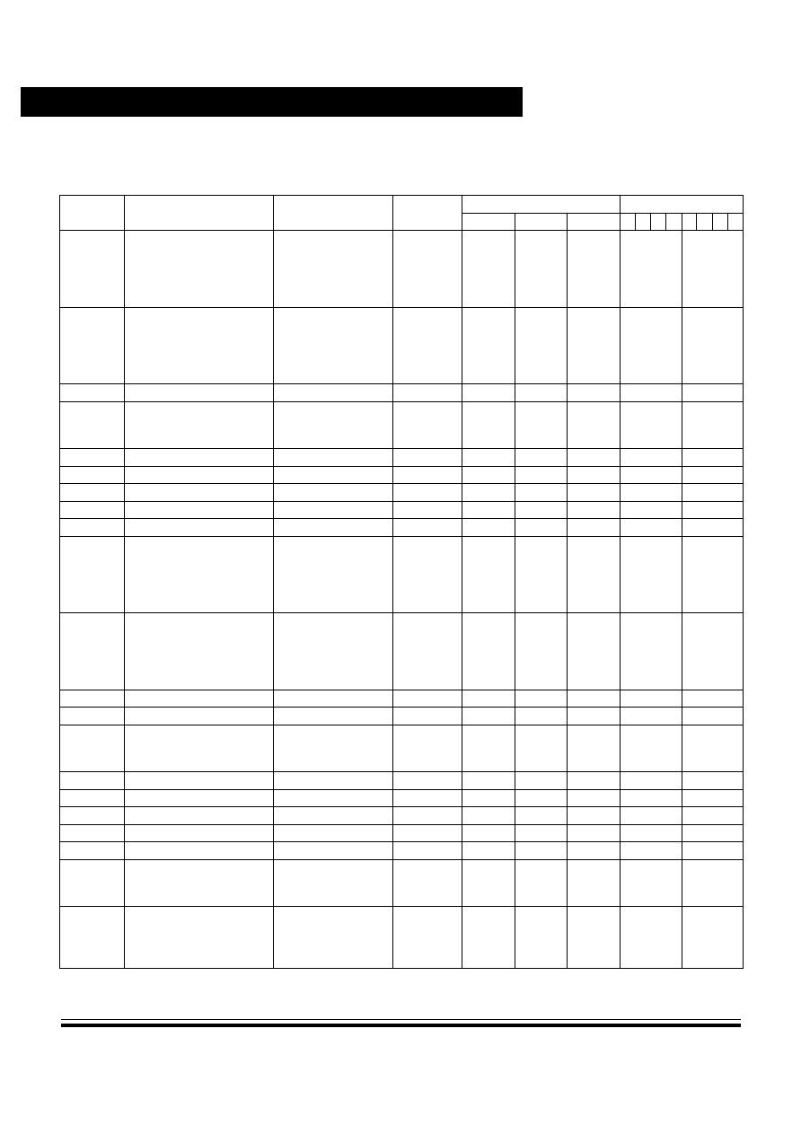
CPU Core and Instruction Set
Technical Data
MC68HC11P2 -- Rev 1.0
226
CPU Core and Instruction Set
MOTOROLA
CPX (opr)
Compare IX with memory (16-
bit)
IX ≠ (M:M+1)
IMM
DIR
EXT
IND, X
IND, Y
8C
9C
BC
AC
CDAC
jj kk
dd
hh ll
ff
ff
4
5
6
6
7
-- -- -- --
CPY (opr)
Compare IY with memory (16-
bit)
IY ≠ (M:M+1)
IMM
DIR
EXT
IND, X
IND, Y
18 8C
18 9C
18 BC
1A AC
18 AC
jj kk
dd
hh ll
ff
ff
5
6
7
7
7
-- -- -- --
DAA
Decimal adjust A
adjust sum to BCD
INH
19
--
2
-- -- -- --
?
DEC (opr)
Decrement memory byte
M ≠ 1
M
EXT
IND, X
IND, Y
7A
6A
18 6A
hh ll
ff
ff
6
6
7
-- -- -- --
--
DECA
Decrement accumulator A
A ≠ 1
A
A INH
4A
--
2
-- -- -- --
--
DECB
Decrement accumulator B
B ≠ 1
B
B INH
5A
--
2
-- -- -- --
--
DES
Decrement stack pointer
SP ≠ 1
SP
INH
34
--
3
-- -- -- -- -- -- -- --
DEX
Decrement index register X
IX ≠ 1
IX
INH
09
--
3
-- -- -- -- --
-- --
DEY
Decrement index register Y
IY ≠ 1
IY
INH
18 09
--
4
-- -- -- -- --
-- --
EORA (opr)
Exclusive OR A with memory
A
M
A
A IMM
A DIR
A EXT
A IND, X
A IND, Y
88
98
B8
A8
18 A8
ii
dd
hh ll
ff
ff
2
3
4
4
5
-- -- -- --
0 --
EORB (opr)
Exclusive OR B with memory
B
M
A
B IMM
B DIR
B EXT
B IND, X
B IND, Y
C8
D8
F8
E8
18 E8
ii
dd
hh ll
ff
ff
2
3
4
4
5
-- -- -- --
0 --
FDIV
Fractional divide, 16 by 16
D / IX
IX; r
D
INH
03
--
41
-- -- -- -- --
IDIV
Integer divide, 16 by 16
D / IX
IX; r
D
INH
02
--
41
-- -- -- -- --
0
INC (opr)
Increment memory byte
M + 1
M
EXT
IND, X
IND, Y
7C
6C
18 6C
hh ll
ff
ff
6
6
7
-- -- -- --
--
INCA
Increment accumulator A
A + 1
A
A INH
4C
--
2
-- -- -- --
--
INCB
Increment accumulator B
B + 1
B
B INH
5C
--
2
-- -- -- --
--
INS
Increment stack pointer
SP + 1
SP
INH
31
--
3
-- -- -- -- -- -- -- --
INX
Increment index register X
IX + 1
IX
INH
08
--
3
-- -- -- -- --
-- --
INY
Increment index register Y
IY + 1
IY
INH
18 08
--
4
-- -- -- -- --
-- --
JMP (opr)
Jump
see
Figure 11-2
EXT
IND, X
IND, Y
7E
6E
18 6E
hh ll
ff
ff
3
3
4
-- -- -- -- -- -- -- --
JSR (opr)
Jump to subroutine
see
Figure 11-2
DIR
EXT
IND, X
IND, Y
9D
BD
AD
18 AD
dd
hh ll
ff
ff
5
6
6
7
-- -- -- -- -- -- -- --
Table 11-2. Instruction set (Sheet 4 of 8)
Mnemonic
Operation
Description
Addressing
mode
Instruction
Condition codes
Opcode
Operand
Cycles
S X H I N Z V C

CPU Core and Instruction Set
Instruction set
MC68HC11P2 -- Rev 1.0
Technical Data
MOTOROLA
CPU Core and Instruction Set
227
LDAA (opr)
Load accumulator A
M
A
A IMM
A DIR
A EXT
A IND, X
A IND, Y
86
96
B6
A6
18 A6
ii
dd
hh ll
ff
ff
2
3
4
4
5
-- -- -- --
0 --
LDAB (opr)
Load accumulator B
M
B
B IMM
B DIR
B EXT
B IND, X
B IND, Y
C6
D6
F6
E6
18 E6
ii
dd
hh ll
ff
ff
2
3
4
4
5
-- -- -- --
0 --
LDD (opr)
Load double accumulator D
M
A; M+1
B
IMM
DIR
EXT
IND, X
IND, Y
CC
DC
FC
EC
18 EC
jj kk
dd
hh ll
ff
ff
3
4
5
5
6
-- -- -- --
0 --
LDS (opr)
Load stack pointer
M:M+1
SP
IMM
DIR
EXT
IND, X
IND, Y
8E
9E
BE
AE
18 AE
jj kk
dd
hh ll
ff
ff
3
4
5
5
6
-- -- -- --
0 --
LDX (opr)
Load index register X
M:M+1
IX
IMM
DIR
EXT
IND, X
IND, Y
CE
DE
FE
EE
CDEE
jj kk
dd
hh ll
ff
ff
3
4
5
5
6
-- -- -- --
0 --
LDY (opr)
Load index register Y
M:M+1
IY
IMM
DIR
EXT
IND, X
IND, Y
18 CE
18 DE
18 FE
1A EE
18 EE
jj kk
dd
hh ll
ff
ff
4
5
6
6
6
-- -- -- --
0 --
LSL (opr)
Logical shift left
EXT
IND, X
IND, Y
78
68
18 68
hh ll
ff
ff
6
6
7
-- -- -- --
LSLA
Logical shift left A
A INH
48
--
2
-- -- -- --
LSLB
Logical shift left B
B INH
58
--
2
-- -- -- --
LSLD
Logical shift left D
INH
05
--
3
-- -- -- --
LSR (opr)
Logical shift right
EXT
IND, X
IND, Y
74
64
18 64
hh ll
ff
ff
6
6
7
-- -- -- -- 0
LSRA
Logical shift right A
A INH
44
--
2
-- -- -- -- 0
LSRB
Logical shift right B
B INH
54
--
2
-- -- -- -- 0
LSRD
Logical shift right D
INH
04
--
3
-- -- -- -- 0
MUL
Multiply, 8 x 8
A * B
D
INH
3D
--
10
-- -- -- -- -- -- --
Table 11-2. Instruction set (Sheet 5 of 8)
Mnemonic
Operation
Description
Addressing
mode
Instruction
Condition codes
Opcode
Operand
Cycles
S X H I N Z V C
b7
b0
C
0
b15
b0
C
0
b7
b0
0
C
b15
b0
0
C
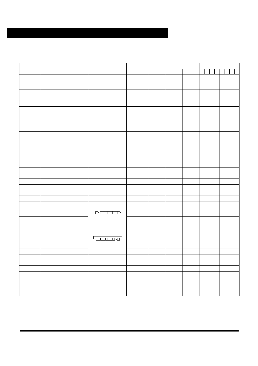
CPU Core and Instruction Set
Technical Data
MC68HC11P2 -- Rev 1.0
228
CPU Core and Instruction Set
MOTOROLA
NEG (opr)
Twos complement memory byte
0 ≠ M
M
EXT
IND, X
IND, Y
70
60
18 60
hh ll
ff
ff
6
6
7
-- -- -- --
NEGA
Twos complement A
0 ≠ A
A
A INH
40
--
2
-- -- -- --
NEGB
Twos complement B
0 ≠ B
B
B INH
50
--
2
-- -- -- --
NOP
No operation
no operation
INH
01
--
2
-- -- -- -- -- -- -- --
ORAA
OR accumulator A (inclusive)
A + M
A
A IMM
A DIR
A EXT
A IND, X
A IND, Y
8A
9A
BA
AA
18 AA
ii
dd
hh ll
ff
ff
2
3
4
4
5
-- -- -- --
0 --
ORAB
OR accumulator B (inclusive)
B + M
B
B IMM
B DIR
B EXT
B IND, X
B IND, Y
CA
DA
FA
EA
18 EA
ii
dd
hh ll
ff
ff
2
3
4
4
5
-- -- -- --
0 --
PSHA
Push A onto stack
A
Stack; SP = SP≠1 A INH
36
--
3
-- -- -- -- -- -- -- --
PSHB
Push B onto stack
B
Stack; SP = SP≠1 B INH
37
--
3
-- -- -- -- -- -- -- --
PSHX
Push IX onto stack (low first)
IX
Stack; SP = SP≠2
INH
3C
--
4
-- -- -- -- -- -- -- --
PSHY
Push IY onto stack (low first)
IY
Stack; SP = SP≠2
INH
18 3C
--
5
-- -- -- -- -- -- -- --
PULA
Pull A from stack
SP = SP+1; Stack
A A INH
32
--
4
-- -- -- -- -- -- -- --
PULB
Pull B from stack
SP = SP+1; Stack
B B INH
33
--
4
-- -- -- -- -- -- -- --
PULX
Pull IX from stack (high first)
SP = SP+2; Stack
IX
INH
38
--
5
-- -- -- -- -- -- -- --
PULY
Pull IY from stack (high first)
SP = SP+2; Stack
IY
INH
18 38
--
6
-- -- -- -- -- -- -- --
ROL (opr)
Rotate left
EXT
IND, X
IND, Y
79
69
18 69
hh ll
ff
ff
6
6
7
-- -- -- --
ROLA
Rotate left A
A INH
49
--
2
-- -- -- --
ROLB
Rotate left B
B INH
59
--
2
-- -- -- --
ROR (opr)
Rotate right
EXT
IND, X
IND, Y
76
66
18 66
hh ll
ff
ff
6
6
7
-- -- -- --
RORA
Rotate right A
A INH
46
--
2
-- -- -- --
RORB
Rotate right B
B INH
56
--
2
-- -- -- --
RTI
Return from interrupt
see
Figure 11-2
INH
3B
--
12
RTS
Return from subroutine
see
Figure 11-2
INH
39
--
5
-- -- -- -- -- -- -- --
SBA
Subtract B from A
A ≠ B
A
INH
10
--
2
-- -- -- --
SBCA (opr)
Subtract with carry from A
A ≠ M ≠ C
A
A IMM
A DIR
A EXT
A IND, X
A IND, Y
82
92
B2
A2
18 A2
ii
dd
hh ll
ff
ff
2
3
4
4
5
-- -- -- --
Table 11-2. Instruction set (Sheet 6 of 8)
Mnemonic
Operation
Description
Addressing
mode
Instruction
Condition codes
Opcode
Operand
Cycles
S X H I N Z V C
b7
b0
C
b7
b0
C

CPU Core and Instruction Set
Instruction set
MC68HC11P2 -- Rev 1.0
Technical Data
MOTOROLA
CPU Core and Instruction Set
229
SBCB (opr)
Subtract with carry from B
B ≠ M ≠ C
B
B IMM
B DIR
B EXT
B IND, X
B IND, Y
C2
D2
F2
E2
18 E2
ii
dd
hh ll
ff
ff
2
3
4
4
5
-- -- -- --
SEC
Set carry
1
C
INH
0D
--
2
-- -- -- -- -- -- -- 1
SEI
Set interrupt mask
1
I
INH
0F
--
2
-- -- -- 1 -- -- -- --
SEV
Set overflow flag
1
V
INH
0B
--
2
-- -- -- -- -- -- 1 --
STAA (opr)
Store accumulator A
A
M
A DIR
A EXT
A IND, X
A IND, Y
97
B7
A7
18 A7
dd
hh ll
ff
ff
3
4
4
5
-- -- -- --
0 --
STAB (opr)
Store accumulator B
B
M
B DIR
B EXT
B IND, X
B IND, Y
D7
F7
E7
18 E7
dd
hh ll
ff
ff
3
4
4
5
-- -- -- --
0 --
STD (opr)
Store accumulator D
A
M; B
M+1
DIR
EXT
IND, X
IND, Y
DD
FD
ED
18 ED
dd
hh ll
ff
ff
4
5
5
6
-- -- -- --
0 --
STOP
Stop internal clocks
--
INH
CF
--
2
-- -- -- -- -- -- -- --
STS (opr)
Store stack pointer
SP
M:M+1
DIR
EXT
IND, X
IND, Y
9F
BF
AF
18 AF
dd
hh ll
ff
ff
4
5
5
6
-- -- -- --
0 --
STX (opr)
Store index register X
IX
M:M+1
DIR
EXT
IND, X
IND, Y
DF
FF
EF
CDEF
dd
hh ll
ff
ff
4
5
5
6
-- -- -- --
0 --
STY (opr)
Store index register Y
IY
M:M+1
DIR
EXT
IND, X
IND, Y
18 DF
18 FF
1A EF
18 EF
dd
hh ll
ff
ff
5
6
6
6
-- -- -- --
0 --
SUBA (opr)
Subtract memory from A
A ≠ M
A
A IMM
A DIR
A EXT
A IND, X
A IND, Y
80
90
B0
A0
18 A0
ii
dd
hh ll
ff
ff
2
3
4
4
5
-- -- -- --
SUBB (opr)
Subtract memory from B
B ≠ M
B
B IMM
B DIR
B EXT
B IND, X
B IND, Y
C0
D0
F0
E0
18 E0
ii
dd
hh ll
ff
ff
2
3
4
4
5
-- -- -- --
SUBD (opr)
Subtract memory from D
D ≠ M:M+1
D
IMM
DIR
EXT
IND, X
IND, Y
83
93
B3
A3
18 A3
jj kk
dd
hh ll
ff
ff
4
5
6
6
7
-- -- -- --
Table 11-2. Instruction set (Sheet 7 of 8)
Mnemonic
Operation
Description
Addressing
mode
Instruction
Condition codes
Opcode
Operand
Cycles
S X H I N Z V C
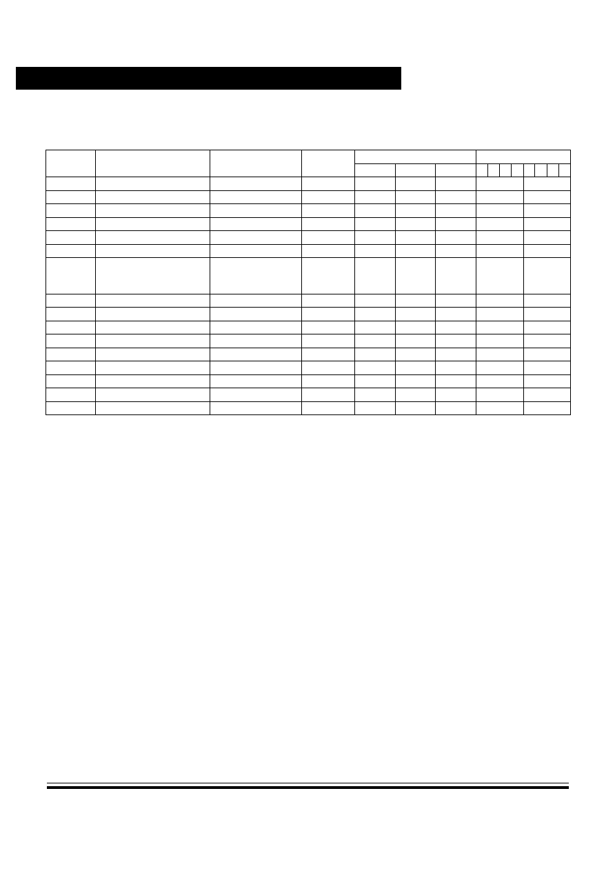
CPU Core and Instruction Set
Technical Data
MC68HC11P2 -- Rev 1.0
230
CPU Core and Instruction Set
MOTOROLA
SWI
Software interrupt
see
Figure 11-2
INH
3F
--
14
-- -- -- 1 -- -- -- --
TAB
Transfer A to B
A
B
INH
16
--
2
-- -- -- --
0 --
TAP
Transfer A to CC register
A
CCR
INH
06
--
2
TBA
Transfer B to A
B
A
INH
17
--
2
-- -- -- --
0 --
TEST
Test (only in test modes)
address bus increments
INH
00
--
-- -- -- -- -- -- -- --
TPA
Transfer CC register to A
CCR
A
INH
07
--
2
-- -- -- -- -- -- -- --
TST (opr)
Test for zero or minus
M ≠ 0
EXT
IND, X
IND, Y
7D
6D
18 6D
hh ll
ff
ff
6
6
7
-- -- -- --
0 0
TSTA
Test A for zero or minus
A ≠ 0
A INH
4D
--
2
-- -- -- --
0 0
TSTB
Test B for zero or minus
B ≠ 0
B INH
5D
--
2
-- -- -- --
0 0
TSX
Transfer stack pointer to X
SP + 1
IX
INH
30
--
3
-- -- -- -- -- -- -- --
TSY
Transfer stack pointer to Y
SP + 1
IY
INH
18 30
--
4
-- -- -- -- -- -- -- --
TXS
Transfer X to stack pointer
IX ≠ 1
SP
INH
35
--
3
-- -- -- -- -- -- -- --
TYS
Transfer Y to stack pointer
IY ≠ 1
SP
INH
18 35
--
4
-- -- -- -- -- -- -- --
WAI
Wait for interrupt
stack registers & WAIT
INH
3E
--
-- -- -- -- -- -- -- --
XGDX
Exchange D with X
IX
D; D
IX
INH
8F
--
3
-- -- -- -- -- -- -- --
XGDY
Exchange D with Y
IY
D; D
IY
INH
18 8F
--
4
-- -- -- -- -- -- -- --
Operators
Operands
Is transferred to
dd
8-bit direct address ($0000≠$00FF); the high byte is assumed
∑ Boolean AND
to be zero
+ Arithmetic addition, except where used as an
ff
8-bit positive offset ($00 to $FF (0 to 256)) is added to the
inclusive-OR symbol in Boolean formulae
contents of the index register
Exclusive-OR
hh
High order byte of 16-bit extended address
* Multiply
ii
One byte of immediate data
: Concatenation
jj
High order byte of 16-bit immediate data
≠ Arithmetic subtraction, or negation symbol
kk
Low order byte of 16-bit immediate data
(Twos complement)
ll
Low order byte of 16-bit extended address
mm 8-bit mask (set bits to be affected)
rr
Signed relative offset ($80 to $7F (≠128 to +127));
offset is relative to the address following the offset byte
Cycles
Condition Codes
Infinite, or until reset occurs
--
Bit not changed
12 cycles are used, beginning with the opcode
0
Bit always cleared
fetch. A wait state is entered, which remains
1
Bit always set
in effect for an integer number of MPU E clock
Bit set or cleared, depending on the operation
cycles (n) until an interrupt is recognized.
Bit can be cleared, but cannot become set
Finally, two additional cycles are used to fetch
?
Not defined
the appropriate interrupt vector. (14 + n, total).
Table 11-2. Instruction set (Sheet 8 of 8)
Mnemonic
Operation
Description
Addressing
mode
Instruction
Condition codes
Opcode
Operand
Cycles
S X H I N Z V C

MC68HC11P2 -- Rev 1.0
Technical Data
MOTOROLA
Electrical Specifications
231
Technical Data -- MC68HC11P2
Section 12. Electrical Specifications
12.1 Contents
12.2
Introduction. . . . . . . . . . . . . . . . . . . . . . . . . . . . . . . . . . . . . . 231
12.3
Maximum ratings . . . . . . . . . . . . . . . . . . . . . . . . . . . . . . . . .232
12.4
Thermal characteristics and power considerations . . . . .233
12.5
Test methods . . . . . . . . . . . . . . . . . . . . . . . . . . . . . . . . . . . . 234
12.6
DC electrical characteristics . . . . . . . . . . . . . . . . . . . . . . . . 235
12.7
Control timing . . . . . . . . . . . . . . . . . . . . . . . . . . . . . . . . . . . .237
12.2 Introduction
This section contains the electrical specifications and associated timing
information for the standard supply voltage (V
DD
= 5V ± 10%)
MC68HC11P2 variants.

Electrical Specifications
Technical Data
MC68HC11P2 -- Rev 1.0
232
Electrical Specifications
MOTOROLA
12.3 Maximum ratings
NOTE:
This device contains circuitry designed to protect against damage due to
high electrostatic voltages or electric fields. However, it is recommended
that normal precautions be taken to avoid the application of any voltages
higher than those given in the maximum ratings table to this high
impedance circuit. For maximum reliability all unused inputs should be
tied to either V
SS
or V
DD
.
Rating
Symbol
Value
Unit
Supply voltage
(1)
1. All voltages are with respect to V
SS
.
V
DD
≠ 0.3 to +7.0
V
Input voltage
(1)
V
in
≠ 0.3 to +7.0
V
Operating temperature range
≠ MC68HC11P2, MC68HC711P2
T
A
T
L
to T
H
≠ 40 to +85
∞C
Storage temperature range
T
stg
≠ 55 to +150
∞C
Current drain per pin
(2)
≠ not VDD, VSS, VDD AD, VSS AD,
VRH or VRL
2. Maximum current drain per pin is for one pin at a time, observing maximum
power dissipation limits.
I
D
25
mA

Electrical Specifications
Thermal characteristics and power considerations
MC68HC11P2 -- Rev 1.0
Technical Data
MOTOROLA
Electrical Specifications
233
12.4 Thermal characteristics and power considerations
The average chip junction temperature, T
J
, in degrees Celsius can be
obtained from the following equation:
[1]
where:
T
A
= Ambient temperature (∞C)
JA
= Package thermal resistance, junction-to-ambient (∞C/W)
P
D
= Total power dissipation = P
INT
+ P
I/O
(W)
P
INT
= Internal chip power = I
DD
∑ V
DD
(W)
P
I/O
= Power dissipation on input and output pins (User determined)
An approximate relationship between P
D
and T
J
(if P
I/O
is neglected) is:
[2]
Solving equations [1] and [2] for K gives:
[3]
where K is a constant for a particular part. K can be determined by
measuring P
D
(at equilibrium) for a known T
A
. Using this value of K, the
values of P
D
and T
J
can be obtained for any value of T
A
, by solving the
above equations. The package thermal characteristics are shown
below:
Characteristics
Symbol
Value
Unit
Thermal resistance
≠ 84-pin PLCC package
≠ 84-pin CERQUAD package (EPROM)
≠ 88-pin QFP package
JA
50
50
TBD
∞C/W
T
J
T
A
P
D
JA
∑
(
)
+
=
P
D
K
T
J
273
+
---------------------
=
K
P
D
T
A
273
+
(
)
∑
JA
P
D
2
∑
+
=

Electrical Specifications
Technical Data
MC68HC11P2 -- Rev 1.0
234
Electrical Specifications
MOTOROLA
12.5 Test methods
Figure 12-1. Test methods
~V
DD
V
DD
R2
R1
C
Test
Point
Pins
R1
R2
C
PA[7:0], PB[7:0], PC[7:0],
PD5, PD0, E, R/W, AS
3.26kæ
2.38kæ
90pF
PD[4:1]
3.26kæ
2.38kæ
200pF
0.4V
V
DD
≠ 0.8V
0.4V
nominal
nominal
~V
SS
70% of V
DD
20% of V
DD
nominal timing
~V
DD
~V
SS
V
DD
≠ 0.8V
0.4V
Clocks,
strobes
Inputs
Outputs
~V
DD
20% of V
DD
spec.
spec.
~V
SS
70% of V
DD
20% of V
DD
spec. timing
~V
DD
~V
SS
Clocks,
strobes
Inputs
Outputs
(a) Equivalent test loads
(b) DC testing
(c) AC testing
20% of V
DD
70% of V
DD
V
DD
≠ 0.8V
(2)
0.4V
(2)
70% of V
DD
20% of V
DD
Notes:
(1) Full test loads are applied during all DC electrical tests and AC timing measurements.
(2) During AC timing measurements, inputs are driven to 0.4V and V
DD
≠ 0.8V;
timing measurements are taken at the 20% and 70% of V
DD
points.
Electrical Specifications
DC electrical characteristics
MC68HC11P2 -- Rev 1.0
Technical Data
MOTOROLA
Electrical Specifications
235
12.6 DC electrical characteristics
(V
DD
= 5.0 Vdc ± 10%, V
SS
= 0 Vdc, T
A
= T
L
to T
H
, unless otherwise noted)
Characteristic
Symbol
Min.
Max.
Unit
Output voltage
(1)
(
I
LOAD
= ± 10 µA
):
All outputs except XTAL
All outputs except XTAL, RESET & MODA
1. V
OH
specification for RESET and MODA is not applicable as they are open-drain pins.
V
OH
specification is not applicable to ports C and D in wired-OR mode.
V
OL
V
OH
--
V
DD
≠ 0.1
0.1
--
V
V
Output high voltage
(1)
(
I
LOAD
= ≠0.8mA, V
DD
=4.5V
):
All outputs except XTAL, RESET & MODA
V
OH
V
DD
≠ 0.8
--
V
Output low voltage (
I
LOAD
= +1.6mA
):
All outputs except XTAL
V
OL
--
0.4
V
Input high voltage:
All inputs except RESET
RESET
V
IH
0.7V
DD
0.8V
DD
V
DD
+ 0.3
V
DD
+ 0.3
V
Input low voltage ≠ all inputs
V
IL
V
SS
≠ 0.3
0.2V
DD
V
I/O ports tristate leakage (
V
IN
= V
IH
or V
IL
):
Ports A, B, C, D, F, G, H, MODA/LIR, RESET
I
OZ
--
±10
µA
Input leakage
(2)
(
V
IN
= V
DD
or V
SS
):
IRQ, XIRQ (ROM parts)
MODB/VSTBY, XIRQ (EPROM parts)
2. Refer to A/D specification for the leakage current value for port E.
I
IN
--
--
±1
±10
µA
Input current with pull-up resistors (
V
IN
= V
IL
):
Ports B, F, G, H
I
IPR
100
500
µA
RAM stand-by voltage (power down)
V
SB
2.0
V
DD
V
RAM stand-by current (power down)
I
SB
--
10
µA
Input capacitance:
Port E, IRQ, XIRQ, EXTAL
Ports A, B, C, D, F, G, H, MODA/LIR, RESET
C
IN
--
--
8
12
pF
Output load capacitance:
All outputs except PD[4:1], XTAL, MODA/LIR
PD[4:1]
C
L
--
--
90
200
pF
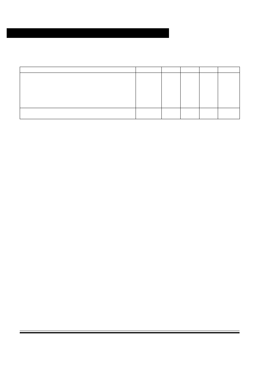
Electrical Specifications
Technical Data
MC68HC11P2 -- Rev 1.0
236
Electrical Specifications
MOTOROLA
Characteristic
Symbol
2MHz
3 MHz
4MHz
Unit
Maximum total supply current (including PLL)
(1)
:
RUN: Single chip mode
RUN: Expanded mode
WAIT: Single chip mode
(2)
WAIT: Expanded mode
(2)
STOP: Single chip mode
I
DD
27
35
10
12
50
32
42
15
17
50
40
50
20
22
50
mA
mA
mA
mA
µA
Power dissipation: Single chip mode
Power dissipation: Expanded mode
P
D
149
193
176
231
220
275
mW
1. All current measurements taken with suitable decoupling capacitors across the power supply to suppress the transient
switching currents inherent in CMOS designs.
EXTAL is driven with a square wave, with t
CYC
= 500/333/250ns for 2/3/4MHz devices.
VIL 0.2V; VIH
VDD ≠ 0.2V; no DC loads
WAIT: all peripheral functions shut down
STOP: all clocks stopped
2. If the PLL low-power WAIT mode is selected (WEN = 1) then, with an external clock of 614kHz, the supply current will not
exceed 1mA in single chip mode, or 2mA in expanded mode.

Electrical Specifications
Control timing
MC68HC11P2 -- Rev 1.0
Technical Data
MOTOROLA
Electrical Specifications
237
12.7 Control timing
(V
DD
= 5.0 Vdc ± 10%, V
SS
= 0 Vdc, T
A
= T
L
to T
H
)
Characteristic
(1)
1. All timing is given with respect to 20% and 70% of V
DD
, unless otherwise noted.
Symbol
2.0MHz
3.0MHz
4.0MHz
Unit
Min.
Max.
Min.
Max.
Min.
Max.
Frequency of operation
f
OP
0
2.0
0
3.0
0
4.0
MHz
E clock period
t
CYC
500
--
333
--
250
--
ns
Crystal frequency
f
XTAL
--
8.0
--
12.0
--
16.0
MHz
External oscillator frequency
4f
OP
0
8.0
0
12.0
0
16.0
MHz
Processor control set-up time
(t
PCSU
= t
CYC
/4 + 50ns)
t
PCSU
175
--
133
--
112
--
ns
Reset input pulse width
(2)
2. Reset is recognized during the first clock cycle it is held low. Internal circuitry then drives the pin low for four clock cycles,
releases the pin and samples the pin level two cycles later to determine the source of the interrupt. (See
Resets and Inter-
rupts
.)
PW
RSTL
(3)
PW
RSTL
(4)
3. To guarantee an external reset vector.
4. This is the minimum input time; it can be pre-empted by an internal reset.
8
1
--
--
8
1
--
--
8
1
--
--
t
CYC
Mode programming set-up time
t
MPS
2
--
2
--
2
--
t
CYC
Mode programming hold time
t
MPH
10
--
10
--
10
--
ns
Interrupt pulse width (IRQ edge sensitive mode)
PW
IRQ
t
CYC
+20
--
t
CYC
+20
--
t
CYC
+20
--
ns
Timer pulse width
(Input capture and pulse accumulator inputs)
PW
TIM
t
CYC
+20
--
t
CYC
+20
--
t
CYC
+20
--
ns
WAIT recovery start-up time
t
WRS
--
4
--
4
--
4
t
CYC
Clock monitor reset
f
CMON
10
200
10
200
10
200
kHz
PLL crystal frequency
f
XTAL
--
2.0
--
2.0
--
2.0
MHz
PLL stabilization time
t
PLLS
--
TBD
--
TBD
--
TBD
ms
Figure 12-2. Timer inputs
PW
TIM
Notes
PA[3:0]
(2)
PA[3:0]
(1)
PA7
(1), (3)
PA7
(2), (3)
(1) Rising edge sensitive input.
(2) Falling edge sensitive input.
(3) Maximum pulse accumulator clocking rate is E clock frequency divided by two (E/2).

Electrical Specifications
Technical Data
MC68HC11P2 -- Rev 1.0
238
Electrical Specifications
MOTOROLA
Figure 12-3. Reset timing
Figure 12-4. Interrupt timing
FFFF
FFFE
FFFE
FFFE
FFFE
FFFE
New
FFFF
FFFE
FFFE
FFFE
FFFE
PC
New
PC
V
DD
EXTAL
E
RESET
MODA,
Address
MODB
4064 t
CYC
t
PCSU
PW
RSTL
t
MPS
t
MPH
VA+1
VA
SP≠8
SP≠5
E clock
Address
(3)
OA
Notes:
SP≠3
SP≠8
SP
OA+1
R/W
t
PCSU
SP≠7
SP≠4
SP≠2
SP≠1
New
PC
SP≠6
PW
IRQ
≠ ≠
PCL
PCH
IYL
IYH
OP
IXL
IXH
B
A
CCR
≠ ≠
VH
VL
OP
Data
(4)
IRQ
(1)
IRQ
(2)
, XIRQ
or internal
interrupt
(1) Edge sensitive IRQ pin (IRQE = 1).
(2) Level sensitive IRQ pin (IRQE = 0).
(3) Where OA = Opcode address and VA = Vector address.
(4) Where OP = Opcode, VH = Vector (MSB) and VL = Vector (LSB).

Electrical Specifications
Control timing
MC68HC11P2 -- Rev 1.0
Technical Data
MOTOROLA
Electrical Specifications
239
Figure 12-5. STOP recovery timing
Figure 12-6. WAIT recovery timing
FFF3
FFF2
SP≠8
SP≠8
SP≠7
SP...
SA+2
New
PC
Internal
IRQ
(1)
E clock
Address
(5)
clocks
SA+1
SA
(6)
SA+1
SA+1
SA
(6)
SA+1
Op-
code
Address
(4)
PW
IRQ
t
STOPDELAY
(3)
IRQ
(2)
or XIRQ
Resume program with instruction which follows the STOP instruction
Notes:
(1) Edge sensitive IRQ pin (IRQE = 1).
(2) Level sensitive IRQ pin (IRQE = 0).
(3) t
STOPDELAY
= 4064 t
CYC
(DLY = 1) or 4 t
CYC
(DLY = 0).
(4) XIRQ with X-bit in CCR = 1.
(5) IRQ (or XIRQ, with X-bit = 0; in this case vector fetch will be $FFF4/5).
(6) SA = STOP address.
VA+1
VA
(2)
SP≠8
SP≠8
E clock
Address
WA
(1)
WA+1
Notes:
RESET also causes recovery from WAIT.
(1) WA = WAIT address.
(2) VA = Vector address.
SP≠8
SP≠8...SP≠8
SP≠8
SP≠2...SP≠8
SP≠1
SP
New
PC
IRQ, XIRQ,
or internal
interrupts
R/W
t
PCSU
t
WRS
Stack registers

Electrical Specifications
Technical Data
MC68HC11P2 -- Rev 1.0
240
Electrical Specifications
MOTOROLA
12.7.1 Peripheral port timing
(V
DD
= 5.0 Vdc ± 10%, V
SS
= 0 Vdc, T
A
= T
L
to T
H
)
Characteristic
(1)
1. All timing is given with respect to 20% and 70% of V
DD
, unless otherwise noted.
Symbol
2.0MHz
3.0MHz
4.0MHz
Unit
Min.
Max.
Min.
Max.
Min.
Max.
Frequency of operation (E clock frequency)
f
OP
0
2.0
0
3.0
0
4.0
MHz
E clock period
t
CYC
500
--
333
--
250
--
ns
Peripheral data set-up time, all ports
(2)
2. Port C and D timing is valid for active drive (CWOM and DWOM bits clear in OPT2 and SPCR registers, respectively).
t
PDSU
100
--
100
--
100
--
ns
Peripheral data hold time, all ports
(2)
t
PDH
50
--
50
--
50
--
ns
Delay time, peripheral data write
MCU write to port A, B, G or H
MCU write to port C, D or F
t
PWD
--
--
200
225
--
--
200
183
--
--
200
162
ns
Figure 12-7. Port read timing diagram
Figure 12-8. Port write timing diagram
MCU read of port
E clock
Ports
A, C, D, F
Ports
t
PDSU
t
PDH
t
PDSU
t
PDH
B, E, G, H
t
PWD
MCU write to port
t
PWD
Previous port data
New data valid
Previous port data
New data valid
E clock
Ports
C, D, F
Ports
A, B, G, H

Electrical Specifications
Control timing
MC68HC11P2 -- Rev 1.0
Technical Data
MOTOROLA
Electrical Specifications
241
12.7.2 Analog-to-digital converter characteristics
(V
DD
= 5.0 Vdc ± 10%, V
SS
= 0 Vdc, T
A
= T
L
to T
H
, 750 kHz
E
4MHz, unless otherwise noted)
Characteristic
Parameter
Min.
Absolute
2MHz
(1)
1. For f
OP
< 2MHz, source impedances should be approximately 10kæ. For f
OP
2MHz, source impedances should be in the
range 5≠10kæ. Source impedances greater than 10kæ have an adverse affect on A/D accuracy, because of input leakage.
3 MHz
(1)
4MHz
(1)
Unit
Max.
Max.
Max.
Resolution
Number of bits resolved by ADC
--
8
--
--
--
bits
Non-linearity
Maximum deviation from the ideal ADC
transfer characteristics
--
--
±0.5
±1
±1
LSB
Zero error
Difference from the output of an ideal ADC for
zero input voltage
--
--
±0.5
±1
±1
LSB
Full-scale
error
Difference from the output of an ideal ADC for
full-scale input voltage
--
--
±0.5
±1
±1
LSB
Total
unadjusted
error
Maximum sum of non-linearity, zero and full-
scale errors
--
--
±0.5
±1.5
±1.5
LSB
Quantization
error
Uncertainty due to converter resolution
--
--
±0.5
±0.5
±0.5
LSB
Absolute
accuracy
Difference between the actual input voltage
and the full-scale weighted equivalent of the
binary output code, including all error sources
--
--
±1
±2
±2
LSB
Conversion
range
Analog input voltage range
V
RL
--
V
RH
V
RH
V
RH
V
V
RH
Analog reference voltage (high)
(2)
2. Performance verified down to
V
R
= 2.5V, however accuracy is tested and guaranteed at
V
R
= 5V ± 10%.
V
RL
--
V
DD
+0.1 V
DD
+0.1 V
DD
+0.1
V
V
RL
Analog reference voltage (low)
(2)
V
SS
≠0.1
--
V
RH
V
RH
V
RH
V
V
R
Minimum difference between V
RH
and V
RL
(2)
3
--
--
--
--
V
Conversion
time
Total time to perform a single A/D conversion:
E clock
Internal RC oscillator
--
--
32
--
--
t
CYC
+32
--
t
CYC
+32
--
t
CYC
+32
t
CYC
µs
Monotonicity
Conversion result never decreases with an
increase in input voltage and has no missing codes
Guaranteed
Zero input
reading
Conversion result when V
IN
= V
RL
$00
--
--
--
--
Hex
Full-scale
reading
Conversion result when V
IN
= V
RH
--
--
$FF
$FF
$FF
Hex
Sample
acquisition
time
Analogue input acquisition sampling time:
E clock
Internal RC oscillator
--
--
12
--
--
12
--
12
--
12
t
CYC
µs
Sample/hold
capacitance
Input capacitance (PE[0:7]) during sample
--
20 (typ)
--
--
--
pF
Input
leakage
Input leakage on A/D pins:
PE[0:7]
V
RL
, V
RH
--
--
--
--
400
1.0
400
1.0
400
1.0
nA
µA

Electrical Specifications
Technical Data
MC68HC11P2 -- Rev 1.0
242
Electrical Specifications
MOTOROLA
12.7.3 Serial peripheral interface timing
(V
DD
= 5.0 Vdc ± 10%, V
SS
= 0 Vdc, T
A
= T
L
to T
H
)
Num
Characteristic
(1)
1. All timing is given with respect to 20% and 70% of V
DD
, unless otherwise noted.
Symbol
2.0MHz
3.0MHz
4.0MHz
Unit
Min.
Max.
Min.
Max.
Min.
Max.
Operating frequencyMaster
Slave
f
OP(M)
f
OP(S)
0
0
0.5
2.0
0
0
0.5
3.0
0
0
0.5
4.0
f
OP
MHz
1
Cycle timeMaster
Slave
t
CYC(M)
t
CYC(S)
2.0
500
--
--
2.0
333
--
--
2.0
250
--
--
t
CYC
ns
2
Enable lead time
(2)
Master
Slave
2. Signal production depends on software.
t
LEAD(M)
t
LEAD(S)
--
250
--
--
--
240
--
--
--
200
--
--
ns
3
Enable lag time
(2)
Master
Slave
t
LAG(M)
t
LAG(S)
--
250
--
--
--
240
--
--
--
200
--
--
ns
4
Clock (SCK) high timeMaster
Slave
t
W(SCKH)
M
t
W(SCKH)S
340
190
--
--
227
127
--
--
130
85
--
--
ns
5
Clock (SCK) low timeMaster
Slave
t
W(SCKL)M
t
W(SCKL)S
340
190
--
--
227
127
--
--
130
85
--
--
ns
6
Input data set-up timeMaster
Slave
t
SU(M)
t
SU(S)
100
100
--
--
100
100
--
--
100
100
--
--
ns
7
Input data hold timeMaster
Slave
t
H(M)
t
H(S)
100
100
--
--
100
100
--
--
100
100
--
--
ns
8
Access time (from high-z to data active)
Slave
t
A
0
120
0
120
0
120
ns
9
Disable time (hold time to high-z state)Slave
t
DIS
--
240
--
167
--
125
ns
10
Data valid (after enable edge)
(3)
3. Assumes 200pF load on all SPI pins.
t
V(S)
--
240
--
167
--
125
ns
11
Output data hold time (after enable edge)
t
HO
0
--
0
--
0
--
ns
12
Rise time
(3)
SPI outputs (SCK, MOSI and MISO)
SPI inputs (SCK, MOSI, MISO and SS)
t
RM
t
RS
--
--
100
2.0
--
--
100
2.0
--
--
100
2.0
ns
µs
13
Fall time
(3)
SPI outputs (SCK, MOSI and MISO)
SPI inputs (SCK, MOSI, MISO and SS)
t
FM
t
FS
--
--
100
2.0
--
--
100
2.0
--
--
100
2.0
ns
µs

Electrical Specifications
Control timing
MC68HC11P2 -- Rev 1.0
Technical Data
MOTOROLA
Electrical Specifications
243
Figure 12-9. SPI master timing (CPHA = 0)
Figure 12-10. SPI master timing (CPHA = 1)
1
SS
(input)
SCK (CPOL=0)
(output)
SCK (CPOL=1)
(output)
MISO
(input)
MOSI
(output)
(see note)
(see note)
SS is held high on master
MSB in
LSB in
Bit 6......1
Master MSB out
Bit 6......1
Master LSB out
13
12
13
5
4
4
5
7
11
10
12
13
6
10 (ref.)
11 (ref.)
12
Note: This first clock edge is generated internally, but is not seen at the SCK pin.
1
SS
(input)
SCK (CPOL=0)
(output)
SCK (CPOL=1)
(output)
MISO
(input)
MOSI
(output)
(see note)
SS is held high on master
MSB in
LSB in
Bit 6......1
Master MSB out
Bit 6......1
Master LSB out
12
13
12
5
4
4
5
11
10
12
13
10 (ref.)
11 (ref.)
13
Note: This last clock edge is generated internally, but is not seen at the SCK pin.
(see note)
7
6
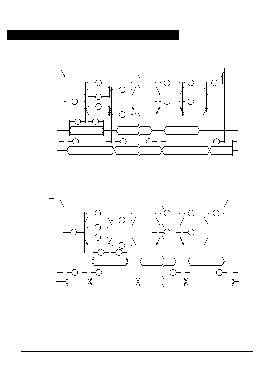
Electrical Specifications
Technical Data
MC68HC11P2 -- Rev 1.0
244
Electrical Specifications
MOTOROLA
Figure 12-11. SPI slave timing (CPHA = 0)
Figure 12-12. SPI slave timing (CPHA = 1)
1
SS
(input)
SCK (CPOL=0)
(input)
SCK (CPOL=1)
(input)
MOSI
(input)
MISO
(output)
MSB in
LSB in
Bit 6......1
Slave MSB out
Bit 6......1
Slave LSB out
12
13
12
5
4
4
5
8
11
13
Note: Not defined, but normally the MSB of character just received.
7
6
10
(see note)
9
3
2
1
SS
(input)
SCK (CPOL=0)
(input)
SCK (CPOL=1)
(input)
MOSI
(input)
MISO
(output)
MSB in
LSB in
Bit 6......1
Slave MSB out
Bit 6......1
Slave LSB out
12
13
12
5
4
4
5
8
11
13
Note: Not defined, but normally the LSB of character last transmitted.
7
6
10
(see note)
9
3
2

Electrical Specifications
Control timing
MC68HC11P2 -- Rev 1.0
Technical Data
MOTOROLA
Electrical Specifications
245
12.7.4 Nonmultiplexed expansion bus timing
(V
DD
= 5.0 Vdc ± 10%, V
SS
= 0 Vdc, T
A
= T
L
to T
H
)
Num
Characteristic
(1)
1. All timing is given with respect to 20% and 70% of V
DD
, unless otherwise noted.
Symbol
2.0MHz
3.0MHz
4.0MHz
Unit
Min.
Max.
Min.
Max.
Min.
Max.
Frequency of operation (E clock frequency)
f
OP
0
2.0
0
3.0
0
4.0
MHz
1
E clock period
t
CYC
500
--
333
--
250
--
ns
2
Pulse width, E low
(2), (3)
2. Input clock duty cycles other than 50% will affect the bus performance.
3. For f
OP
2MHz the following formulae may be used to calculate parameter values:
PW
EL
= t
CYC
/2 ≠ 20ns PW
EH
= t
CYC
/2 ≠ 25ns
t
AH
= t
CYC
/8 ≠ 10ns t
AD
= t
CYC
/8 + 40ns
t
AV
= PW
EL
≠ t
AD
t
DHW
= t
CYC
/8
t
ACCA
= t
CYC
≠ t
f
≠ t
DSR
≠ t
AD
t
DSW
= PW
EH
≠ t
DDW
t
ECSA
= PW
EH
≠ t
ECSD
≠ t
DSR
t
ACSD
= t
CYC
/4 + 40ns
t
ACSA
= t
CYC
≠ t
f
≠ t
DSR
≠ t
ACSD
PW
EL
230
--
147
--
105
--
ns
3
Pulse width, E high
(2), (3)
PW
EH
225
--
142
--
100
--
ns
4A
4B
E clockrise time
fall time
t
r
t
f
--
--
20
20
--
--
20
18
--
--
20
15
ns
9
Address hold time
(3)
t
AH
53
--
32
--
21
--
ns
11
Address delay time
(3)
t
AD
--
103
--
82
--
71
ns
12
Address valid to E rise time
(3)
t
AV
127
--
65
--
34
--
ns
17
Read data set-up time
t
DSR
30
--
30
--
20
--
ns
18
Read data hold time
t
DHR
0
--
0
--
0
--
ns
19
Write data delay time
t
DDW
--
40
--
40
--
40
ns
21
Write data hold time
(3)
t
DHW
63
--
42
--
31
--
ns
29
MPU address access time
(3)
t
ACCA
347
--
203
--
144
--
ns
39
Write data set-up time
(3)
t
DSW
185
--
102
--
60
--
ns
57
Address valid to data tristate time
t
AVDZ
--
10
--
10
--
10
ns

Electrical Specifications
Technical Data
MC68HC11P2 -- Rev 1.0
246
Electrical Specifications
MOTOROLA
12.7.5 EEPROM characteristics
12.7.6 EPROM characteristics
Figure 12-13. Expansion bus timing
Characteristic
Temperature range
Unit
≠40 to +85∞C
≠40 to +105∞C
≠40 to +125∞C
Programming time
(1)
<1MHz, RCO enabled
1≠2MHz, RCO disabled
2MHz & whenever RCO enabled
1. The RC oscillator (RCO) must be enabled (by setting the CSEL bit in the OPTION register) for EEPROM programming
and erasure when the E clock frequency is less than 1.0MHz.
10
20
10
15
must use RCO
15
20
must use RCO
20
ms
Erase time: byte, row and bulk
(1)
10
10
10
ms
Write/erase endurance
(2)
2. Refer to the current issue of Motorola's quarterly Reliability Monitor Report for the latest failure rate information.
10000
10 000
10000
cycles
Data retention
(2)
10
10
10
years
(V
DD
= 5.0 Vdc ± 10%, V
SS
= 0 Vdc, T
A
= T
L
to T
H
, unless otherwise noted)
Characteristic
Symbol
Min.
Typ.
Max.
Unit
Programming voltage
V
PPE
11.75
12.25
12.75
V
Programming time
t
EPROG
2
2
4
ms
E clock
R/W,
Address
Data
(read)
Data
(write)
1
2
3
4B
4A
12
11
9
18
21
39
17
29
57
19

MC68HC11P2 -- Rev 1.0
Technical Data
MOTOROLA
Mechanical Data
247
Technical Data -- MC68HC11P2
Section 13. Mechanical Data
13.1 Contents
13.2
Pin assignments . . . . . . . . . . . . . . . . . . . . . . . . . . . . . . . . . . 248
13.3
Package dimensions . . . . . . . . . . . . . . . . . . . . . . . . . . . . . . 249
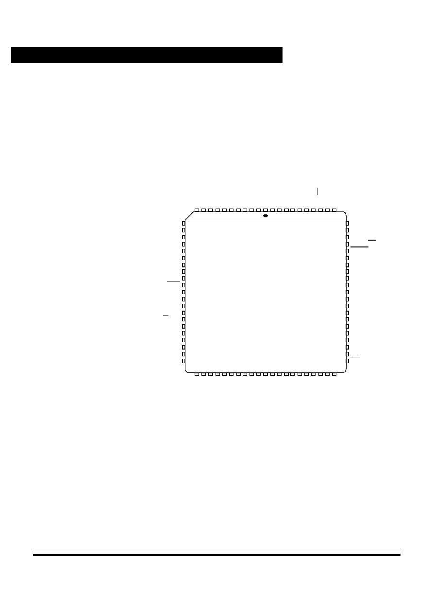
Mechanical Data
Technical Data
MC68HC11P2 -- Rev 1.0
248
Mechanical Data
MOTOROLA
13.2 Pin assignments
The MC68HC11P2 is available in 84-pin PLCC or 88-pin QFP packages;
in addition to those two packages, the MC68HC711P2 is also available
in a windowed 84-pin CERQUAD package, to allow full use of the
EPROM .
Figure 13-1. 84-pin PLCC/CERQUAD pinout
PB0
/A8
PB1
/A9
P
B
2/A
1
0
PB3
/A1
1
P
B
4/A
1
2
P
B
5/A
1
3
P
B
6/A
1
4
P
B
7/A
1
5
VSS
VD
D
P
A
0
/IC
3
P
A
1
/IC
2
P
A
2
/IC
1
P
A
3/
O
C
1/
O
C
5
/
I
C
4
P
A
4/
O
C
1/
O
C
4
P
A
5
/
OC1
/
OC
3
P
A
6
/
OC1
/
OC
2
P
A
7/
O
C
1/
P
A
I
PD
5/SS
PD
4/
SC
K
PD
3/
MOSI
PG0
VD
D AD
AD
7/
PE
7
AD
6/
PE
6
AD
5/
PE
5
AD
4/
PE
4
AD
3/
PE
3
AD
2/
PE
2
AD
1/
PE
1
AD
0/
PE
0
VR
L
VR
H
VSS
A
D
A7
/
P
F
7
A6
/PF6
A5
/
P
F
5
A4
/
P
F
4
A3
/PF3
A2
/PF2
A1
/PF1
A0
/PF0
74
73
72
71
70
69
68
67
66
65
64
63
62
61
60
59
58
57
56
55
54
12
13
14
15
16
17
18
19
20
21
22
23
24
25
26
27
28
29
30
31
32
33
34
35
36
37
38
39
40
41
42
43
44
45
46
47
48
49
50
51
52
53
11
10
9
8
7
6
5
4
3
2
84
83
82
81
80
79
78
77
76
75
PD2/MISO
PD1/TXD1
PD0/RXD1
MODA/LIR
RESET
XFC
VDDSYN
EXTAL
XTAL
E
VDDR
VSSR
PC7/D7
PC6/D6
PC5/D5
PC4/D4
PC3/D3
PC2/D2
PC1/D1
PC0/D0
IRQ
PW1/PH0
PW2/PH1
PW3/PH2
PW4/PH3
RXD2/PH4
TXD2/PH5
RXD3/PH6
TXD3/PH7
MODB/VSTBY
XIRQ
VDD
VDDL
VSSL
VSS
R/W/PG7
PG6
PG5
PG4
PG3
PG2
PG1

Mechanical Data
Package dimensions
MC68HC11P2 -- Rev 1.0
Technical Data
MOTOROLA
Mechanical Data
249
13.3 Package dimensions
Figure 13-2. 84-pin PLCC mechanical dimensions
≠L≠
≠M≠
≠P≠
≠N≠
pin 1
pin 84
V
W
Y brk
Z
R
A
C
J E
G
G1
U
B
G1
Z1
X
0.10
≠T≠
Seating plane
Case No. 780-01
84 lead PLCC
Dim.
Min.
Max.
Notes
Dim.
Min.
Max.
A
30.10
30.35
1. Due to space limitations, this case shall be represented by a
general case outline, rather than one showing all the leads.
2. Datums ≠L≠, ≠M≠, ≠N≠ and ≠P≠ are determined where top of lead
shoulder exits plastic body at mould parting line.
3. Dimension G1, true position to be measured at datum ≠T≠ (seating
plane).
4. Dimensions R and U do not include mould protrusion. Allowable mould
protrusion is 0.25mm per side.
5. Dimensions and tolerancing per ANSI Y 14.5M, 1982.
6. All dimensions in mm.
U
29.21
29.36
B
30.10
30.35
V
1.07
1.21
C
4.20
4.57
W
1.07
1.21
E
2.29
2.79
X
1.07
1.42
F
0.33
0.48
Y
--
0.50
G
1.27 BSC
Z
2∞
10∞
H
0.66
0.81
G1
28.20
28.70
J
0.51
--
K1
1.02
--
K
0.64
--
Z1
2∞
10∞
R
29.21
29.36
(Note 1)
H
K1
K
F
0.18 T N
≠P
L
≠M
M
S
S
S
S
0.18 T L
≠M
N
≠P
M
S
S
S
S
0.18 T L
≠M
N
≠P
M
S
S
S
S
0.18 T N
≠P
L
≠M
M
S
S
S
S
0.25 T L
≠M
N
≠P
S
S
S
S
S
0.18 T N
≠P
L
≠M
M
S
S
S
S
0.18 T L
≠M
N
≠P
M
S
S
S
S
0.18 T N
≠P
L
≠M
M
S
S
S
S
0.18 T L
≠M
N
≠P
M
S
S
S
S
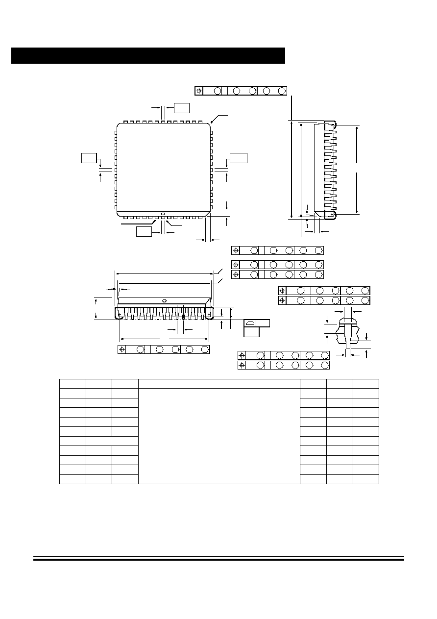
Mechanical Data
Technical Data
MC68HC11P2 -- Rev 1.0
250
Mechanical Data
MOTOROLA
Figure 13-3. 84-pin CERQUAD mechanical dimensions
≠L≠
≠M≠
≠P≠
≠N≠
pin 1
pin 84
V
W
Y brk
Z
R
A
C
J E
G
G1
U
B
G1
Z1
X
0.10
≠T≠
Seating plane
Case No. 780A-01
84 lead CERQUAD
Dim.
Min.
Max.
Notes
Dim.
Min.
Max.
A
30.10
30.35
1. Due to space limitations, this case shall be represented by a
general case outline, rather than one showing all the leads.
2. Datums ≠L≠, ≠M≠, ≠N≠ and ≠P≠ are determined where top of lead
shoulder exits package body at glass parting line.
3. Dimension G1, true position to be measured at datum ≠T≠ (seating
plane).
4. Dimensions R and U do not include glass protrusion. Allowable glass
protrusion is 0.25mm per side.
5. Dimensions and tolerancing per ANSI Y 14.5M, 1982.
6. All dimensions in mm.
U
29.21
29.36
B
30.10
30.35
V
1.07
1.21
C
4.20
4.57
W
1.07
1.21
E
2.29
2.79
X
1.07
1.42
F
0.33
0.53
Y
--
0.50
G
1.27 BSC
Z
2∞
10∞
H
0.66
0.81
G1
28.20
28.70
J
0.51
--
K1
1.02
--
K
0.64
--
Z1
2∞
10∞
R
29.21
29.36
(Note 1)
H
K1
K
F
0.18 T N
≠P
L
≠M
M
S
S
S
S
0.18 T L
≠M
N
≠P
M
S
S
S
S
0.18 T L
≠M
N
≠P
M
S
S
S
S
0.18 T N
≠P
L
≠M
M
S
S
S
S
0.25 T L
≠M
N
≠P
S
S
S
S
S
0.18 T N
≠P
L
≠M
M
S
S
S
S
0.18 T L
≠M
N
≠P
M
S
S
S
S
0.18 T N
≠P
L
≠M
M
S
S
S
S
0.18 T L
≠M
N
≠P
M
S
S
S
S

MC68HC11P2 -- Rev 1.0
Technical Data
MOTOROLA
Ordering Information
251
Technical Data -- MC68HC11P2
Section 14. Ordering Information
14.1 Contents
14.2
Introduction. . . . . . . . . . . . . . . . . . . . . . . . . . . . . . . . . . . . . . 251
14.2 Introduction
Use the information in
Table 14-1
to specify the appropriate device type
when placing an order.
Table 14-1. Ordering information
Package Temperature
CONFIG
register
Description
Frequency
MC order number
84-pin
PLCC
≠40 to +85∞C
$FF
Buffalo ROM
4MHz
MC68HC11P2BCFN4
$XX
Custom ROM
3MHz
4MHz
MC68HC11P2CFN3
MC68HC11P2CFN4
$XX
Custom ROM, No EEPROM
3MHz
4MHz
MC68HC11P3CFN3
MC68HC11P3CFN4
$FD
No ROM
3MHz
4MHz
MC68HC11P1CFN3
MC68HC11P1CFN4
$FC
No ROM or EEPROM
3MHz
4MHz
MC68HC11P0CFN3
MC68HC11P0CFN4
$FF
OTPROM
3MHz
4MHz
MC68HC711P2CFN3
MC68HC711P2CFN4
84-pin
CERQUAD
≠40 to +85∞C
$FF
EPROM
3MHz
4MHz
MC68HC711P2CFS3
MC68HC711P2CFS4

Ordering Information
Technical Data
MC68HC11P2 -- Rev 1.0
252
Ordering Information
MOTOROLA

MC68HC11P2 -- Rev 1.0
Technical Data
MOTOROLA
Development Support
253
Technical Data -- MC68HC11P2
Section 15. Development Support
15.1 Contents
15.2
Introduction. . . . . . . . . . . . . . . . . . . . . . . . . . . . . . . . . . . . . . 253
15.3
EVS -- Evaluation system . . . . . . . . . . . . . . . . . . . . . . . . . . 253
15.2 Introduction
The following information provides a reference to development tools for
the M68HC11 family of microcontrollers. For more detailed information
please refer to the appropriate system manual.
15.3 EVS -- Evaluation system
The EVS is an economical tool for designing, debugging and evaluating
target systems based on the MC68HC11P2 and MC68HC711P2 device
types. The two printed circuit boards that comprise the EVS are the
MC68HC11KMNPEM emulator module and the MC68HC11PFB
platform board. The main features of the EVS are as follows:
∑
Monitor/debugger firmware
∑
Single-line assembler/disassembler
∑
Host computer download capability
Table 15-1. M68HC11 development tools
Devices
Evaluation
boards
Evaluation
modules
Evaluation
systems/kits
Programmer
boards
MC68HC11P2,
MC68HC711P2
--
--
MC68HC11KMNPEVS
--

Development Support
Technical Data
MC68HC11P2 -- Rev 1.0
254
Development Support
MOTOROLA
∑
Dual memory maps:
≠
64K byte monitor map that includes 16K bytes of monitor
EPROM
≠
MC68HC711P2 user map that includes 64K bytes of
emulation RAM
∑
MCU extension I/O port for single chip, expanded and special test
operating modes
∑
RS-232C terminal and host I/O ports
∑
Logic analyser connector

MC68HC11P2 -- Rev 1.0
Technical Data
MOTOROLA
Glossary
255
Technical Data -- MC68HC11P2
Glossary
A -- See "accumulator (A)."
accumulator (A) -- An 8-bit general-purpose register in the CPU08. The CPU08 uses the
accumulator to hold operands and results of arithmetic and logic operations.
acquisition mode -- A mode of PLL operation during startup before the PLL locks on a
frequency. Also see "tracking mode."
address bus -- The set of wires that the CPU or DMA uses to read and write memory locations.
addressing mode -- The way that the CPU determines the operand address for an instruction.
The M68HC08 CPU has 16 addressing modes.
ALU -- See "arithmetic logic unit (ALU)."
arithmetic logic unit (ALU) -- The portion of the CPU that contains the logic circuitry to perform
arithmetic, logic, and manipulation operations on operands.
asynchronous -- Refers to logic circuits and operations that are not synchronized by a common
reference signal.
baud rate -- The total number of bits transmitted per unit of time.
BCD -- See "binary-coded decimal (BCD)."
binary -- Relating to the base 2 number system.
binary number system -- The base 2 number system, having two digits, 0 and 1. Binary
arithmetic is convenient in digital circuit design because digital circuits have two
permissible voltage levels, low and high. The binary digits 0 and 1 can be interpreted to
correspond to the two digital voltage levels.
binary-coded decimal (BCD) -- A notation that uses 4-bit binary numbers to represent the 10
decimal digits and that retains the same positional structure of a decimal number. For
example,
234 (decimal) = 0010 0011 0100 (BCD)
bit -- A binary digit. A bit has a value of either logic 0 or logic 1.

Glossary
Technical Data
MC68HC11P2 -- Rev 1.0
256
Glossary
MOTOROLA
branch instruction -- An instruction that causes the CPU to continue processing at a memory
location other than the next sequential address.
break module -- A module in the M68HC08 Family. The break module allows software to halt
program execution at a programmable point in order to enter a background routine.
breakpoint -- A number written into the break address registers of the break module. When a
number appears on the internal address bus that is the same as the number in the break
address registers, the CPU executes the software interrupt instruction (SWI).
break interrupt -- A software interrupt caused by the appearance on the internal address bus
of the same value that is written in the break address registers.
bus -- A set of wires that transfers logic signals.
bus clock -- The bus clock is derived from the CGMOUT output from the CGM. The bus clock
frequency, f
op
, is equal to the frequency of the oscillator output, CGMXCLK, divided by
four.
byte -- A set of eight bits.
C -- The carry/borrow bit in the condition code register. The CPU08 sets the carry/borrow bit
when an addition operation produces a carry out of bit 7 of the accumulator or when a
subtraction operation requires a borrow. Some logical operations and data manipulation
instructions also clear or set the carry/borrow bit (as in bit test and branch instructions and
shifts and rotates).
CCR -- See "condition code register."
central processor unit (CPU) -- The primary functioning unit of any computer system. The
CPU controls the execution of instructions.
CGM -- See "clock generator module (CGM)."
clear -- To change a bit from logic 1 to logic 0; the opposite of set.
clock -- A square wave signal used to synchronize events in a computer.
clock generator module (CGM) -- A module in the M68HC08 Family. The CGM generates a
base clock signal from which the system clocks are derived. The CGM may include a
crystal oscillator circuit and or phase-locked loop (PLL) circuit.
comparator -- A device that compares the magnitude of two inputs. A digital comparator defines
the equality or relative differences between two binary numbers.
computer operating properly module (COP) -- A counter module in the M68HC08 Family that
resets the MCU if allowed to overflow.

Glossary
MC68HC11P2 -- Rev 1.0
Technical Data
MOTOROLA
Glossary
257
condition code register (CCR) -- An 8-bit register in the CPU08 that contains the interrupt
mask bit and five bits that indicate the results of the instruction just executed.
control bit -- One bit of a register manipulated by software to control the operation of the
module.
control unit -- One of two major units of the CPU. The control unit contains logic functions that
synchronize the machine and direct various operations. The control unit decodes
instructions and generates the internal control signals that perform the requested
operations. The outputs of the control unit drive the execution unit, which contains the
arithmetic logic unit (ALU), CPU registers, and bus interface.
COP -- See "computer operating properly module (COP)."
counter clock -- The input clock to the TIM counter. This clock is the output of the TIM
prescaler.
CPU -- See "central processor unit (CPU)."
CPU08 -- The central processor unit of the M68HC08 Family.
CPU clock -- The CPU clock is derived from the CGMOUT output from the CGM. The CPU
clock frequency is equal to the frequency of the oscillator output, CGMXCLK, divided by
four.
CPU cycles -- A CPU cycle is one period of the internal bus clock, normally derived by dividing
a crystal oscillator source by two or more so the high and low times will be equal. The
length of time required to execute an instruction is measured in CPU clock cycles.
CPU registers -- Memory locations that are wired directly into the CPU logic instead of being
part of the addressable memory map. The CPU always has direct access to the
information in these registers. The CPU registers in an M68HC08 are:
∑
A (8-bit accumulator)
∑
H:X (16-bit index register)
∑
SP (16-bit stack pointer)
∑
PC (16-bit program counter)
∑
CCR (condition code register containing the V, H, I, N, Z, and C
bits)
CSIC -- customer-specified integrated circuit
cycle time -- The period of the operating frequency: t
CYC
= 1/f
OP
.
decimal number system -- Base 10 numbering system that uses the digits zero through nine.

Glossary
Technical Data
MC68HC11P2 -- Rev 1.0
258
Glossary
MOTOROLA
direct memory access module (DMA) -- A M68HC08 Family module that can perform data
transfers between any two CPU-addressable locations without CPU intervention. For
transmitting or receiving blocks of data to or from peripherals, DMA transfers are faster
and more code-efficient than CPU interrupts.
DMA -- See "direct memory access module (DMA)."
DMA service request -- A signal from a peripheral to the DMA module that enables the DMA
module to transfer data.
duty cycle -- A ratio of the amount of time the signal is on versus the time it is off. Duty cycle is
usually represented by a percentage.
EEPROM -- Electrically erasable, programmable, read-only memory. A nonvolatile type of
memory that can be electrically reprogrammed.
EPROM -- Erasable, programmable, read-only memory. A nonvolatile type of memory that can
be erased by exposure to an ultraviolet light source and then reprogrammed.
exception -- An event such as an interrupt or a reset that stops the sequential execution of the
instructions in the main program.
external interrupt module (IRQ) -- A module in the M68HC08 Family with both dedicated
external interrupt pins and port pins that can be enabled as interrupt pins.
fetch -- To copy data from a memory location into the accumulator.
firmware -- Instructions and data programmed into nonvolatile memory.
free-running counter -- A device that counts from zero to a predetermined number, then rolls
over to zero and begins counting again.
full-duplex transmission -- Communication on a channel in which data can be sent and
received simultaneously.
H -- The upper byte of the 16-bit index register (H:X) in the CPU08.
H -- The half-carry bit in the condition code register of the CPU08. This bit indicates a carry from
the low-order four bits of the accumulator value to the high-order four bits. The half-carry
bit is required for binary-coded decimal arithmetic operations. The decimal adjust
accumulator (DAA) instruction uses the state of the H and C bits to determine the
appropriate correction factor.
hexadecimal -- Base 16 numbering system that uses the digits 0 through 9 and the letters A
through F.
high byte -- The most significant eight bits of a word.

Glossary
MC68HC11P2 -- Rev 1.0
Technical Data
MOTOROLA
Glossary
259
illegal address -- An address not within the memory map
illegal opcode -- A nonexistent opcode.
I -- The interrupt mask bit in the condition code register of the CPU08. When I is set, all interrupts
are disabled.
index register (H:X) -- A 16-bit register in the CPU08. The upper byte of H:X is called H. The
lower byte is called X. In the indexed addressing modes, the CPU uses the contents of
H:X to determine the effective address of the operand. H:X can also serve as a temporary
data storage location.
input/output (I/O) -- Input/output interfaces between a computer system and the external world.
A CPU reads an input to sense the level of an external signal and writes to an output to
change the level on an external signal.
instructions -- Operations that a CPU can perform. Instructions are expressed by programmers
as assembly language mnemonics. A CPU interprets an opcode and its associated
operand(s) and instruction.
interrupt -- A temporary break in the sequential execution of a program to respond to signals
from peripheral devices by executing a subroutine.
interrupt request -- A signal from a peripheral to the CPU intended to cause the CPU to
execute a subroutine.
I/O -- See "input/output (I/0)."
IRQ -- See "external interrupt module (IRQ)."
jitter -- Short-term signal instability.
latch -- A circuit that retains the voltage level (logic 1 or logic 0) written to it for as long as power
is applied to the circuit.
latency -- The time lag between instruction completion and data movement.
least significant bit (LSB) -- The rightmost digit of a binary number.
logic 1 -- A voltage level approximately equal to the input power voltage (V
DD
).
logic 0 -- A voltage level approximately equal to the ground voltage (V
SS
).
low byte -- The least significant eight bits of a word.
low voltage inhibit module (LVI) -- A module in the M68HC08 Family that monitors power
supply voltage.

Glossary
Technical Data
MC68HC11P2 -- Rev 1.0
260
Glossary
MOTOROLA
LVI -- See "low voltage inhibit module (LVI)."
M68HC08 -- A Motorola family of 8-bit MCUs.
mark/space -- The logic 1/logic 0 convention used in formatting data in serial communication.
mask -- 1. A logic circuit that forces a bit or group of bits to a desired state. 2. A photomask used
in integrated circuit fabrication to transfer an image onto silicon.
mask option -- A optional microcontroller feature that the customer chooses to enable or
disable.
mask option register (MOR) -- An EPROM location containing bits that enable or disable
certain MCU features.
MCU -- Microcontroller unit. See "microcontroller."
memory location -- Each M68HC08 memory location holds one byte of data and has a unique
address. To store information in a memory location, the CPU places the address of the
location on the address bus, the data information on the data bus, and asserts the write
signal. To read information from a memory location, the CPU places the address of the
location on the address bus and asserts the read signal. In response to the read signal,
the selected memory location places its data onto the data bus.
memory map -- A pictorial representation of all memory locations in a computer system.
microcontroller -- Microcontroller unit (MCU). A complete computer system, including a CPU,
memory, a clock oscillator, and input/output (I/O) on a single integrated circuit.
modulo counter -- A counter that can be programmed to count to any number from zero to its
maximum possible modulus.
monitor ROM -- A section of ROM that can execute commands from a host computer for testing
purposes.
MOR -- See "mask option register (MOR)."
most significant bit (MSB) -- The leftmost digit of a binary number.
multiplexer -- A device that can select one of a number of inputs and pass the logic level of that
input on to the output.
N -- The negative bit in the condition code register of the CPU08. The CPU sets the negative bit
when an arithmetic operation, logical operation, or data manipulation produces a negative
result.
nibble -- A set of four bits (half of a byte).

Glossary
MC68HC11P2 -- Rev 1.0
Technical Data
MOTOROLA
Glossary
261
object code -- The output from an assembler or compiler that is itself executable machine code,
or is suitable for processing to produce executable machine code.
opcode -- A binary code that instructs the CPU to perform an operation.
open-drain -- An output that has no pullup transistor. An external pullup device can be
connected to the power supply to provide the logic 1 output voltage.
operand -- Data on which an operation is performed. Usually a statement consists of an
operator and an operand. For example, the operator may be an add instruction, and the
operand may be the quantity to be added.
oscillator -- A circuit that produces a constant frequency square wave that is used by the
computer as a timing and sequencing reference.
OTPROM -- One-time programmable read-only memory. A nonvolatile type of memory that
cannot be reprogrammed.
overflow -- A quantity that is too large to be contained in one byte or one word.
page zero -- The first 256 bytes of memory (addresses $0000≠$00FF).
parity -- An error-checking scheme that counts the number of logic 1s in each byte transmitted.
In a system that uses odd parity, every byte is expected to have an odd number of logic
1s. In an even parity system, every byte should have an even number of logic 1s. In the
transmitter, a parity generator appends an extra bit to each byte to make the number of
logic 1s odd for odd parity or even for even parity. A parity checker in the receiver counts
the number of logic 1s in each byte. The parity checker generates an error signal if it finds
a byte with an incorrect number of logic 1s.
PC -- See "program counter (PC)."
peripheral -- A circuit not under direct CPU control.
phase-locked loop (PLL) -- A oscillator circuit in which the frequency of the oscillator is
synchronized to a reference signal.
PLL -- See "phase-locked loop (PLL)."
pointer -- Pointer register. An index register is sometimes called a pointer register because its
contents are used in the calculation of the address of an operand, and therefore points to
the operand.
polarity -- The two opposite logic levels, logic 1 and logic 0, which correspond to two different
voltage levels, V
DD
and V
SS
.
polling -- Periodically reading a status bit to monitor the condition of a peripheral device.

Glossary
Technical Data
MC68HC11P2 -- Rev 1.0
262
Glossary
MOTOROLA
port -- A set of wires for communicating with off-chip devices.
prescaler -- A circuit that generates an output signal related to the input signal by a fractional
scale factor such as 1/2, 1/8, 1/10 etc.
program -- A set of computer instructions that cause a computer to perform a desired operation
or operations.
program counter (PC) -- A 16-bit register in the CPU08. The PC register holds the address of
the next instruction or operand that the CPU will use.
pull -- An instruction that copies into the accumulator the contents of a stack RAM location. The
stack RAM address is in the stack pointer.
pullup -- A transistor in the output of a logic gate that connects the output to the logic 1 voltage
of the power supply.
pulse-width -- The amount of time a signal is on as opposed to being in its off state.
pulse-width modulation (PWM) -- Controlled variation (modulation) of the pulse width of a
signal with a constant frequency.
push -- An instruction that copies the contents of the accumulator to the stack RAM. The stack
RAM address is in the stack pointer.
PWM period -- The time required for one complete cycle of a PWM waveform.
RAM -- Random access memory. All RAM locations can be read or written by the CPU. The
contents of a RAM memory location remain valid until the CPU writes a different value or
until power is turned off.
RC circuit -- A circuit consisting of capacitors and resistors having a defined time constant.
read -- To copy the contents of a memory location to the accumulator.
register -- A circuit that stores a group of bits.
reserved memory location -- A memory location that is used only in special factory test modes.
Writing to a reserved location has no effect. Reading a reserved location returns an
unpredictable value.
reset -- To force a device to a known condition.
ROM -- Read-only memory. A type of memory that can be read but cannot be changed (written).
The contents of ROM must be specified before manufacturing the MCU.
SCI -- See "serial communication interface module (SCI)."
serial -- Pertaining to sequential transmission over a single line.

Glossary
MC68HC11P2 -- Rev 1.0
Technical Data
MOTOROLA
Glossary
263
serial communications interface module (SCI) -- A module in the M68HC08 Family that
supports asynchronous communication.
serial peripheral interface module (SPI) -- A module in the M68HC08 Family that supports
synchronous communication.
set -- To change a bit from logic 0 to logic 1; opposite of clear.
shift register -- A chain of circuits that can retain the logic levels (logic 1 or logic 0) written to
them and that can shift the logic levels to the right or left through adjacent circuits in the
chain.
signed -- A binary number notation that accommodates both positive and negative numbers.
The most significant bit is used to indicate whether the number is positive or negative,
normally logic 0 for positive and logic 1 for negative. The other seven bits indicate the
magnitude of the number.
software -- Instructions and data that control the operation of a microcontroller.
software interrupt (SWI) -- An instruction that causes an interrupt and its associated vector
fetch.
SPI -- See "serial peripheral interface module (SPI)."
stack -- A portion of RAM reserved for storage of CPU register contents and subroutine return
addresses.
stack pointer (SP) -- A 16-bit register in the CPU08 containing the address of the next available
storage location on the stack.
start bit -- A bit that signals the beginning of an asynchronous serial transmission.
status bit -- A register bit that indicates the condition of a device.
stop bit -- A bit that signals the end of an asynchronous serial transmission.
subroutine -- A sequence of instructions to be used more than once in the course of a program.
The last instruction in a subroutine is a return from subroutine (RTS) instruction. At each
place in the main program where the subroutine instructions are needed, a jump or branch
to subroutine (JSR or BSR) instruction is used to call the subroutine. The CPU leaves the
flow of the main program to execute the instructions in the subroutine. When the RTS
instruction is executed, the CPU returns to the main program where it left off.
synchronous -- Refers to logic circuits and operations that are synchronized by a common
reference signal.
TIM -- See "timer interface module (TIM)."

Glossary
Technical Data
MC68HC11P2 -- Rev 1.0
264
Glossary
MOTOROLA
timer interface module (TIM) -- A module used to relate events in a system to a point in time.
timer -- A module used to relate events in a system to a point in time.
toggle -- To change the state of an output from a logic 0 to a logic 1 or from a logic 1 to a logic 0.
tracking mode -- Mode of low-jitter PLL operation during which the PLL is locked on a
frequency. Also see "acquisition mode."
two's complement -- A means of performing binary subtraction using addition techniques. The
most significant bit of a two's complement number indicates the sign of the number (1
indicates negative). The two's complement negative of a number is obtained by inverting
each bit in the number and then adding 1 to the result.
unbuffered -- Utilizes only one register for data; new data overwrites current data.
unimplemented memory location -- A memory location that is not used. Writing to an
unimplemented location has no effect. Reading an unimplemented location returns an
unpredictable value. Executing an opcode at an unimplemented location causes an illegal
address reset.
V --The overflow bit in the condition code register of the CPU08. The CPU08 sets the V bit when
a two's complement overflow occurs. The signed branch instructions BGT, BGE, BLE,
and BLT use the overflow bit.
variable -- A value that changes during the course of program execution.
VCO -- See "voltage-controlled oscillator."
vector -- A memory location that contains the address of the beginning of a subroutine written
to service an interrupt or reset.
voltage-controlled oscillator (VCO) -- A circuit that produces an oscillating output signal of a
frequency that is controlled by a dc voltage applied to a control input.
waveform -- A graphical representation in which the amplitude of a wave is plotted against time.
wired-OR -- Connection of circuit outputs so that if any output is high, the connection point is
high.
word -- A set of two bytes (16 bits).
write -- The transfer of a byte of data from the CPU to a memory location.
X -- The lower byte of the index register (H:X) in the CPU08.
Z -- The zero bit in the condition code register of the CPU08. The CPU08 sets the zero bit when
an arithmetic operation, logical operation, or data manipulation produces a result of $00.

MC68HC11P2 -- Rev 1.0
Technical Data
MOTOROLA
Revision History
265
Technical Data -- MC68HC11P2
Revision History
15.4 Major Changes Between Revision 1.0 and Revision 0.0
The following table lists the major changes between the current revision
of the MC68HC11P2 Technical Data Book, Rev 1.0, and the previous
revision, Rev 0.0.
Section affected
Page
number
Description of change
General Description
19
SCI2 pins TXD2 and RXD2 corrected to PH7 and PH6
SCI3 pins TXD3 and RXD3 corrected to PH5 and PH4
Pin Descriptions
35
22
Parallel Input/Output
82
Serial Communications
Interface (SCI)
104
Motorola Interconnect
Bus (MI BUS)
110
Mechanical Data
248
Electrical
Specifications
246
Min and max columns added to EPROM Characteristics

Revision History
Technical Data
MC68HC11P2 -- Rev 1.0
266
Revision History
MOTOROLA


HOW TO REACH US:
USA/EUROPE/LOCATIONS NOT LISTED:
Motorola Literature Distribution;
P.O. Box 5405, Denver, Colorado 80217
1-303-675-2140 or 1-800-441-2447
JAPAN:
Motorola Japan Ltd.; SPS, Technical Information Center,
3-20-1, Minami-Azabu Minato-ku, Tokyo 106-8573 Japan
81-3-3440-3569
ASIA/PACIFIC:
Motorola Semiconductors H.K. Ltd.;
Silicon Harbour Centre, 2 Dai King Street,
Tai Po Industrial Estate, Tai Po, N.T., Hong Kong
852-26668334
TECHNICAL INFORMATION CENTER:
1-800-521-6274
HOME PAGE:
http://www.motorola.com/semiconductors
Information in this document is provided solely to enable system and software
implementers to use Motorola products. There are no express or implied copyright
licenses granted hereunder to design or fabricate any integrated circuits or
integrated circuits based on the information in this document.
Motorola reserves the right to make changes without further notice to any products
herein. Motorola makes no warranty, representation or guarantee regarding the
suitability of its products for any particular purpose, nor does Motorola assume any
liability arising out of the application or use of any product or circuit, and specifically
disclaims any and all liability, including without limitation consequential or incidental
damages. "Typical" parameters which may be provided in Motorola data sheets
and/or specifications can and do vary in different applications and actual
performance may vary over time. All operating parameters, including "Typicals"
must be validated for each customer application by customer's technical experts.
Motorola does not convey any license under its patent rights nor the rights of
others. Motorola products are not designed, intended, or authorized for use as
components in systems intended for surgical implant into the body, or other
applications intended to support or sustain life, or for any other application in which
the failure of the Motorola product could create a situation where personal injury or
death may occur. Should Buyer purchase or use Motorola products for any such
unintended or unauthorized application, Buyer shall indemnify and hold Motorola
and its officers, employees, subsidiaries, affiliates, and distributors harmless
against all claims, costs, damages, and expenses, and reasonable attorney fees
arising out of, directly or indirectly, any claim of personal injury or death associated
with such unintended or unauthorized use, even if such claim alleges that Motorola
was negligent regarding the design or manufacture of the part.
Motorola and the Stylized M Logo are registered in the U.S. Patent and Trademark
Office. digital dna is a trademark of Motorola, Inc. All other product or service
names are the property of their respective owners. Motorola, Inc. is an Equal
Opportunity/Affirmative Action Employer.
© Motorola, Inc. 2002
MC68HC11P2/D