 | –≠–ª–µ–∫—Ç—Ä–æ–Ω–Ω—ã–π –∫–æ–º–ø–æ–Ω–µ–Ω—Ç: MPC17511 | –°–∫–∞—á–∞—Ç—å:  PDF PDF  ZIP ZIP |

MPC17511 :MAR.08. 2002 REV.0.5
SMARTMOS
R
MPC17511
16PIN SVM
1 Channel H-Bridge Driver IC
MPC17511 is a monolithic type SMOS5AP
SMARTMOS IC built in 1channel H-Bridge
Driver constituted LDMOSFET, input section
can be directly interfaced from the MCU.
This IC can control 4 mode output function
(Forward, Reverse, Brake, Open) by input logic.
This IC can drive various type of micro motor
and low loss.
Features
-
Manufactured by SMOS5AP process technology
-
Built in Charge-pump Circuit
1
MPC17511
1
2
3
4
5
6
7
8
C2L
C1L
VM
VC
EN
*SMARTMOS is a registered trademark of Motorola Inc.
*Specifications in this data sheet may be changed without prior notice.
14
13
12
11
10
9
16
15
C2H
TSWITCH
OUTB
PGND
OUTA
LGND
IN1
IN2
C1H
VG
IN3
Product Preview
(Top View)
Pin Connections
-
Built in 1 Channel Circuit of H-Bridge Driver
-
4 Mode Drive(Forward, Reverse, Brake, Open)
-
Direct Interface from the MCU
-
Low ON-Resistance Ron=0.6 ohm(Max.)
-
IDR=1.0A (Cont.)
-
Low Consumption Power
-
Built in Shoot Through Current Prevention Circuit
-
Built in Low Voltage Shutdown Circuit
-
PWM Control frequency 200kHz(Max.)
-
Comes in 16-pin VMFP
(pin pitch : 0.65mm)
M
F
r
e
e
s
c
a
l
e
S
e
m
i
c
o
n
d
u
c
t
o
r
,
I
n
c
.
.
.
Freescale Semiconductor, Inc.
For More Information On This Product,
Go to: www.freescale.com
MPC17511 :MAR.08. 2002 REV.0.5
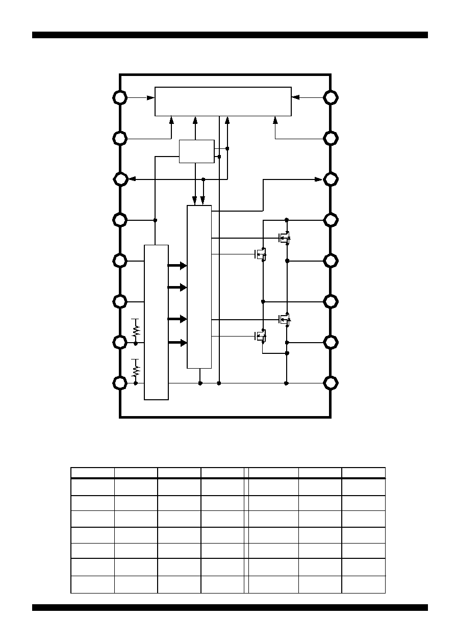
Block Diagram
2
C
o
n
t
r
o
l
L
o
g
i
c
TSWITCH
OUTB
PGND
5
OUTA
16
LGND
3
VG
IN1
8
C1H
IN2
C2H
C2L
C1L
VC
Low voltage
Detector
OSC,
Charge Pump
L
e
v
e
l
S
h
i
f
t
e
r
P
r
e
d
r
i
v
e
r
*Each GND pin are connected by Metal.
13
12
9
4
11
14
10
6
2
1
15
IN3
EN
VM
7
EN
IN1
OUTA
OUTB
IN2
L
L
X
H
H
IN3
H
TSWITCH
X
L
H
X
L
H
H
X
H
L
X
H
H
L
X
Z
Z
X
L
H
L
X
L
L
X
X
L
X
L
X
X
H
X
H
X
L
X
X
L
X
H
X
H
Function Table
Z : High impedance
X : Don't care
vc
vc
F
r
e
e
s
c
a
l
e
S
e
m
i
c
o
n
d
u
c
t
o
r
,
I
n
c
.
.
.
Freescale Semiconductor, Inc.
For More Information On This Product,
Go to: www.freescale.com

MPC17511 :MAR.08. 2002 REV.0.5
Maximum Ratings
3
*1
Driver Circuit Power Supply Voltage
Control Circuit Power Supply Voltage
Singnal Input Voltage
Driver Output Current (continuous)
Driver Output Current (pulsed)
*2
Operating Junction Temperature
Thermal Resistance
*3
Rating
Symbol
Min.
Max.
Unit
VM
VC
VIN
IDR
IDRp
Tj
Tstg
R
ja
- 0.5
8.0
- 0.5
7.0
- 0.5
VC+0.5
1.0
3.0
150
150
150
---
---
- 55
V
V
V
A
A
*2) Ta=25C, Peak time is within 10ms at intervals 0.2seconds.
*3) 37 X 50 X 1.6[mm] glass EPOXY Board mount.
*1) Device may be damaged when used over the ratings.
Driver Circuit Power Supply Voltage
Control Circuit Power Supply Voltage
Signal Input Voltage
Operating Ambient Temperature
Characteristics
Symbol
Min.
Unit
VM
VC
VIN
Topr
2.0
0
-20
---
V
V
V
FIN
kHz
Pulse Input Frequency
Input Pulse Rise Time
TR
TF
Input Pulse Fall Time
us
---
Recommended Operating Condition
us
Storage Temperature Range
---
Max.
6.8
5.7
VC
65
200
1.0
1.0
C
Capacitor for Charge Pump
C1,C2,C3
---
Pre-Driver Circuit Power Supply Voltage
VG
- 0.5
14.0
V
2.7
0.01
1.0
uF
Pre-Driver Circuit Power Supply Voltage
VG
V
13.5
12
Typ.
5.0
5.0
---
25
---
---
---
0.1
13
Power Dissipation
*4
PD
830
---
mW
deg./W
*4) Ta=25C
degC
degC
F
r
e
e
s
c
a
l
e
S
e
m
i
c
o
n
d
u
c
t
o
r
,
I
n
c
.
.
.
Freescale Semiconductor, Inc.
For More Information On This Product,
Go to: www.freescale.com

MPC17511 :MAR.08. 2002 REV.0.5
4
Driver Circuit Power Supply Current
Control Circuit Power Supply Current
Logic Input Function
High Level Input Voltage
Characteristics
Symbol
Min.
Max.
Unit
IMO
ICO
VIH
A
1.0
1.0
---
---
V
V
DC CHARACTERISTICS
Typ.
Quiescent Power Supply Current
us
uA
mA
1.5
---
---
---
uA
Low Level Input Voltage
Driver Output ON Resistance
VIL
RON
VCx0.7
VCx0.3
---
---
ohm
B
F
*1) ICO includes current to the pre-driver circuit.
*4) IDR=1.0[A] source+sink
(Ta=25C, VC=VM=5.0V, GND=0V)
Turn-ON time
Rise time
Characteristics
Symbol
Min.
Max.
Unit
tPLH
tPHL
0.5
---
---
0.1
Typ.
Output Propagation Delay Time
Turn-Off time
us
3.0
---
1.0
0.60
---
0.46
High Level Input Current
Low Level Input Current
IIH
IIL
- 1.0
---
---
---
uA
Low Voltage Detection Circuit
VCDET
2.5
2.0
11.2
V
tPLH
50%
10%
IN1,IN2
OUTA,OUTB
12
10
Detection Voltage
*3) 2.7V < VC < 5.7V
50%
90%
Charge-pump Output Voltage
---
VG
12.8
13
V
C
1.0
Charge-pump Output Voltage (IG=-1mA)
VGload
V
---
D
*5) When no input logic signal.
Charge-pump Circuit
D
0.5
0.1
tVGON
ms
C
tPHL
*1) When C1=C2=C3=0.1[uF]
---
*1
*2
*3
*4
*5
*6) Detection voltage is defined output become High-impedance when VC voltage is dropped.
Test
circuit
E
AC CHARACTERISTICS
(Ta=25C, VC=VM=5.0V, GND=0V )
Test
circuit
*1
tPLH,tPHL (tSON,tSOFF)Timing Chart
When the gate voltage VG is applied from an external source, VG=7.5[V]
---
F
Low Voltage Detection Circuit
tVCDET
Detection time
---
ms
tVCDETon
50%
0%(<1uA)
VC
IM
50%
90%
tVCDEToff
tVCDET Timing Chart
1.5
10
2.5
VCDETon
VCDEToff
Pre-Driver Circuit Power Supply Current
Control Circuit Power Supply Current
IG
IC
G
3.0
0.7
---
---
Active Power Supply Current
mA
mA
---
---
*6
*2) IC include s current to the pre-driver circuit. IC:Fin100kHz. IG:Fin20kHz.
Pullup Resistance (EN,IN3)
Rup
50
kohm
200
100
us
Turn-ON time
tSON
tSOFF
0.5
---
---
0.15
TSWITCH Propagation Delay Time
Turn-Off time
us
C2
0.5
0.15
(IN3)
(TSWITCH)
(tSON)
(tSOFF)
TSWITCH OUT
IOUT=-50uA
IIN=50uA
VOH
VOL
VG-0.5
VG
VG-0.1
V
LGND
LGND+0.5
LGND+0.1
V
B
F
r
e
e
s
c
a
l
e
S
e
m
i
c
o
n
d
u
c
t
o
r
,
I
n
c
.
.
.
Freescale Semiconductor, Inc.
For More Information On This Product,
Go to: www.freescale.com
MPC17511 :MAR.08. 2002 REV.0.5
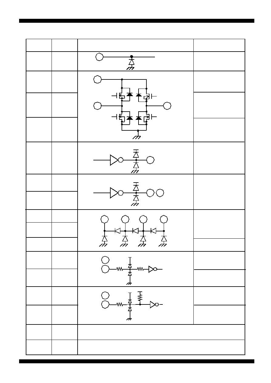
5
Symbol
PIN No.
Simplified Circuit Schematic
Function
VC
5
VM
OUTA
C1L
IN2
4
VC
11
C2L
C1H
C2H
2
13
16
3
VC
VG
C1H
C2H
EN
IN3
15
VG
LGND
IN1
VC
Pin Description
OUTB
TSWITCH
14
9
4
11
13
5
1
1
3
5
16
15
6
7
8
10
9
10
Control Circuit
Power Supply Pin
Driver Power Supply
Voltage Input Pin
Driver Output Pin
Output pin of
Driver Output Pin
Logic GND Pin
These pins connect
to charge pump
capacitors.
(Negative pole)
These pins connect
to charge pump
capacitors.
(Positive pole)
Pre-Driver Circuit
Power Supply Pin
Control Signal
Input Pin 1
Control Signal
Input Pin 2
Enable Control
Signal Input Pin
Signal Input Pin 3
VC
14
step≈|up voltage
6
7
VC
Control Signal
for TSWITCH
PGND
12
Driver GND Pin
2
VC
F
r
e
e
s
c
a
l
e
S
e
m
i
c
o
n
d
u
c
t
o
r
,
I
n
c
.
.
.
Freescale Semiconductor, Inc.
For More Information On This Product,
Go to: www.freescale.com