MPC2104
∑
MPC2105
∑
MPC2106
∑
MPC2107
1
MOTOROLA FAST SRAM
Advance Information
256KB and 512KB BurstRAM
TM
Secondary Cache Modules for
PowerPC
TM
PReP/CHRP Platforms
The MPC2104/5/6/7 are designed to provide burstable, high performance L2
cache for the PowerPC 60x microprocessor family in conformance with the
PowerPC Reference Platform (PReP) and the PowerPC Common Hardware
Reference Platform (CHRP) specifications. These products utilize synchronous or
asynchronous data RAMs.
The MPC2104, MPC2105, and MPC2106 utilize synchronous BurstRAMs.
The modules are configured as 32K x 72, 64K x 72, and 128K x 72 bits in a 182
(91 x 2) pin DIMM format. The MPC2104 uses four of Motorola's 5 V 32K x 18;
the MPC2105 uses four of the 5 V 64K x 18; the MPC2106 uses eight of the
5 V 64K x 18. For tag bits, a 5 V cache tag RAM configured as 16K x 12 for tag field
plus 16K x 2 for valid and dirty status bits is used.
Bursts can be initiated with the ADS signal. Subsequent burst addresses are
generated internal to the BurstRAM by the CNTEN signal.
Write cycles are internally self timed and are initiated by the rising edge of the
clock (CLKx) inputs. Eight write enables are provided for byte write control.
The MPC2107 utilizes asynchronous data RAMs. The module is configured as
32K x 64 in the same 182 pin DIMM format. Again, 5 V cache tag RAMs configured
as 16K x 12 for tag field plus 16K x 2 for valid and dirty status bits are used. Burst
capability is provided in that two burst addresses bypass the address latch.
Presence detect pins are available for auto configuration of the cache con-
trol. A serial EEPROM is optional to provide more in≠depth description of the
cache module. This EEPROM will be available on future revisions of the module
family.
The module family pinout will support 5 V and 3.3 V components for a clear
path to lower voltage and power savings. Both power supplies must be connected.
All of these cache modules are plug and pin compatible with each other.
∑
PowerPC≠style Burst Counter on Chip (MPC2104/5/6)
∑
Flow≠Through Data I/O (MPC2104/5/6)
∑
Plug and Pin Compatibility of entire Module Family
∑
Multiple Clock Pins for Reduced Loading
∑
All Cache Data and Tag I/Os are LVTTL (3.3 V) Compatible (MPC2104/5/6)
∑
Three State Outputs
∑
Byte Write Capability
∑
Fast Module Clock Rates: Up to 66 MHz
∑
Fast SRAM Access Times: 10 ns for Tag RAM Match
9 ns for Data RAM (MPC2104/5/6)
15 ns for Data RAM (MPC2107)
∑
Decoupling Capacitors for Each Fast Static RAM
∑
High Quality Multi≠Layer FR4 PWB With Separate Power and Ground Planes
∑
182 Pin Card Edge Module
∑
Burndy Connector, Part Number: ELF182JSC≠3Z50
BurstRAM is a trademark of Motorola.
PowerPC is a trademark of International Business Machines Corp.
This document contains information on a new product. Specifications and information herein are subject to change without notice.
Order this document
by MPC2104/D
MOTOROLA
SEMICONDUCTOR TECHNICAL DATA
MPC2104
MPC2105
MPC2106
MPC2107
11/8/95
©
Motorola, Inc. 1995
PIN ASSIGNMENT
182≠LEAD DIMM
TOP VIEW ≠ CASE TBD
VSS
PD1/IDSDATA
PD3
DH31
DH29
DH27
DH25
VCC3
CWE3
DH23
DH21
DH18
VSS
DH16
CWE2
DH14
DH13
VCC5
DH10
DH8
CWE1
DH6
VCC3
DH4
VSS
CLK0
VSS
DH1
CWE0
DL31
DL30
VSS
DL29
DL27
DL25
VCC5
CWE7
DL23
DL21
DL19
VSS
DL17
92
93
94
95
96
97
98
99
100
101
102
103
104
105
106
107
108
109
110
111
112
113
114
115
116
117
118
119
120
121
122
123
124
125
126
127
128
129
130
131
132
133
1
2
3
4
5
6
7
8
9
10
11
12
13
14
15
16
17
18
19
20
21
22
23
24
25
26
27
28
29
30
31
32
33
34
35
36
37
38
39
40
41
42
VSS
PD0/IDSCLK
PD2
DH30
DH28
DH26
DH24
VCC3
DP3
DH22
DH20
DH19
VSS
DH17
DP2
DH15
DH12
VCC5
DH11
DH9
DP1
DH7
VCC3
DH5
DH3
DH2
DH0
DP0
VSS
CLK1
VSS
DL28
DL26
DL24
DP7
VCC5
DL22
DL20
DL18
DL16
VSS
DP6
134
135
136
137
138
139
140
141
142
143
144
145
146
147
148
149
150
151
152
153
154
155
156
157
158
159
160
161
162
163
164
165
166
167
168
169
170
171
172
173
174
175
176
177
178
179
180
181
182
43
44
45
46
47
48
49
50
51
52
53
54
55
56
57
58
59
60
61
62
63
64
65
66
67
68
69
70
71
72
73
74
75
76
77
78
79
80
81
82
83
84
85
86
87
88
89
90
91
CWE6
DL15
DL13
VSS
DL10
DL8
CWE5
DL6
VCC3
DL5
DL2
VSS
CLK3
VSS
CLK4
VSS
CWE4
ALE
VCC3
ADDR1
RESERVED
CNTEN0
CNTEN1
VCC5
VCC5
A27
A24
A22
A20
VSS
A18
A16
A15
A14
VCC3
A10
A8
A6
VSS
A4
A2
A1
BURSTMODE
VCC5
VALIDIN
TWE
STANDBY
DIRTYOUT
VSS
DL14
DL12
DL11
VSS
DL9
DP5
DL7
DL4
VCC3
DL3
DL1
DL0
VSS
CLK2
VSS
DP4
COE0
COE1
VCC3
ADDR0
RESERVED
ADS0
ADS1
VCC5
VCC5
A28
A26
A25
A23
VSS
A21
A19
A17
A13
VCC3
A12
A11
A9
VSS
A7
A5
A3
A0
VCC5
TCLR
MATCH
TOE
DIRTYIN
VSS
NOTES:
1. VCC5 and VCC3 must be connected on all modules.
MPC2104
∑
MPC2105
∑
MPC2106
∑
MPC2107
2
MOTOROLA FAST SRAM

MPC2104
∑
MPC2105
∑
MPC2106
∑
MPC2107
4
MOTOROLA FAST SRAM
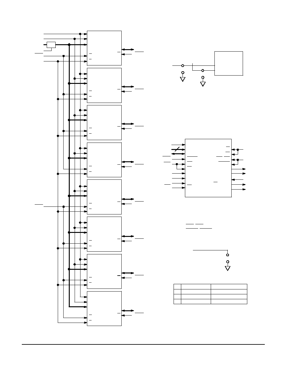
MPC2106 BLOCK DIAGRAM
64K X 18 BURST
K
G
E
DQ0 ≠ DQ8
STANDBY
TSC
COE0
A13 ≠ A26
A0 ≠ A15
A13 ≠ A28
LW
BAA
ADS0
CWE0
A0 ≠ A11
TCLR
TWE
CLK2
MATCH
DIRTYOUT
VALIDIN
DIRTYIN
TOE
TAG: 16K x 12 + V + D
A0 ≠ A13
RESET
TAH, TAG, TAD
SFUNC, SG
TDQ0 ≠ TDQ11
SW
TW
K
MATCH
DIRTYQ
VALIDD
DIRTYD
TG
ALE
= NC
ADDR0
= NC
ADDR1
= NC
PD2
= NC
PD3
X24C00
(OPTIONAL)
SCL
SDA
PD0/IDSCLK
PD1/IDSDATA
J0
DQ9 ≠ DQ17
UW
CLK0
DH0 ≠ DH7 + DP0
DH8 ≠ DH15 + DP1
CWE1
CNTEN0
64K X 18 BURST
K
G
E
DQ0 ≠ DQ8
TSC
A0 ≠ A15
LW
BAA
CWE2
DQ9 ≠ DQ17
UW
CLK1
DH16 ≠ DH23 + DP2
DH24 ≠ DH31 + DP3
CWE3
64K X 18 BURST
K
G
E
DQ0 ≠ DQ8
TSC
A0 ≠ A15
LW
BAA
CWE4
DQ9 ≠ DQ17
UW
CLK3
DL0 ≠ DL7 + DP4
DL8 ≠ DL15 + DP5
CWE5
64K X 18 BURST
K
G
E
DQ0 ≠ DQ8
TSC
A0 ≠ A15
LW
BAA
CWE6
DQ9 ≠ DQ17
UW
CLK4
DL16 ≠ DL23 + DP6
DL24 ≠ DL31 + DP7
CWE7
'244
TT1, WTD
PWRDN
VSS
VCC5
via 100
WTQ
TA, VALIDQ
VCCQ
VCC3
NC
1M
EEPROM 1M
J1
0
no stuff
J0
0
no stuff
A12
64K X 18 BURST
K
G
E
DQ0 ≠ DQ8
TSC
A0 ≠ A15
LW
BAA
CWE0
DQ9 ≠ DQ17
UW
CLK0
DH0 ≠ DH7 + DP0
DH8 ≠ DH15 + DP1
CWE1
64K X 18 BURST
K
G
E
DQ0 ≠ DQ8
TSC
A0 ≠ A15
LW
BAA
CWE2
DQ9 ≠ DQ17
UW
CLK1
DH16 ≠ DH23 + DP2
DH24 ≠ DH31 + DP3
CWE3
64K X 18 BURST
K
G
E
DQ0 ≠ DQ8
TSC
A0 ≠ A15
LW
BAA
CWE4
DQ9 ≠ DQ17
UW
CLK3
DL0 ≠ DL7 + DP4
DL8 ≠ DL15 + DP5
CWE5
64K X 18 BURST
K
G
E
DQ0 ≠ DQ8
TSC
A0 ≠ A15
LW
BAA
CWE6
DQ9 ≠ DQ17
UW
CLK4
DL16 ≠ DL23 + DP6
DL24 ≠ DL31 + DP7
CWE7
COE1
ADS1
CNTEN1
E2
E1
A12
VDD
A13 ≠ A26
A0 ≠ A11
TCLR
TWE
CLK2
MATCH
DIRTYOUT
VALIDIN
DIRTYIN
TOE
TAG: 16K x 12 + V + D
A0 ≠ A13
RESET
TAH, TAG, TAD
SFUNC, SG
TDQ0 ≠ TDQ11
SW
TW
K
MATCH
DIRTYQ
VALIDD
DIRTYD
TG
TT1, WTD
PWRDN
VSS
VCC5
via 100
WTQ
TA, VALIDQ
VCCQ
VCC3
NC
E2
E1
VSS
A12
Note: All 64K X 18 TSP signals are tied to VCC via a 100
resistor. Edge connector A28 connects to the 64K x 18 A0; edge
connector A27 connects to the 64K x 18 A1.
J1
14
PAL
PA12
PA12L
NC
NC