MOTOROLA
SEMICONDUCTOR TECHNICAL DATA
1
REV 2
©
Motorola, Inc. 1997
2/97
Low Voltage PLL Clock Driver
The MPC990/991 is a 3.3V compatible, PLL based ECL/PECL clock
driver. The fully differential design ensures optimum skew and PLL jitter
performance. The performance of the MPC990/991 makes the device
ideal for Workstation, Mainframe Computer and Telecommunication
applications. The MPC990 and MPC991 devices are identical except in
the interface to the reference clock for the PLL. The MPC990 offers an
on≠board crystal oscillator as the PLL reference while the MPC991 offers
a differential ECL/PECL input for applications which need to lock to an
existing clock signal. Both designs offer a secondary single≠ended ECL
clock for system test capabilities.
∑
Fully Integrated PLL
∑
Output Frequency Up to 400MHz
∑
ECL/PECL Inputs and Outputs
∑
Operates from a 3.3V Supply
∑
Output Frequency Configurable
∑
TQFP Packaging
∑
±
50ps Cycle≠to≠Cycle Jitter
The MPC990/991 offers three banks of outputs which can each be
programmed via the the four fsel pins of the device. There are 16 different
output frequency configurations available in the device. The
configurations include output ratios of 1:1, 2:1, 3:1, 3:2, 4:1, 4:3, 4:3:1 and
4:3:2. The programming table in this data sheet illustrates the various
programming options. The SYNC output monitors the relationship
between the Qa and Qc output banks. The output pulses per the timing
diagrams in this data sheet signal the coincident edges of the two output
banks. This feature is useful for non binary relationships between output frequencies (i.e., 3:2 or 4:3 relationships). The Sync_Sel
input toggles the Qd outputs between sync signals and extensions to the Qc bank of outputs.
The MPC990/991 provides a separate output for the feedback to the PLL. This allows for the feedback frequency to be
programmed independently of the other outputs allowing for unique input vs output frequency relationships. The fselFB inputs
provide 6 different feedback frequencies from the QFB differential output pair.
The MPC990/991 features an external differential ECL/PECL feedback to the PLL. This external feedback feature allows for
the MPC991's use as a "zero" delay buffer. The propagation delay between the input reference and the output is dependent on
the input reference frequency. The selection of higher reference frequencies will provide near zero delay through the device.
The PLL_En, Ref_Sel and the Test_Clk input pins provide a means of bypassing the PLL and driving the output buffers
directly. This allows the user to single step a design during system debug. Note that the Test_Clk input is routed through the
dividers so that depending on the programming several edges on the Test_Clk input will be needed to get corresponding edge
transitions on the outputs. The VCO_Sel input provides a means of recentering the VCO to provide a broader range of VCO
frequencies for stable PLL operation.
If the frequency select or the VCO_Sel pins are changed during operation, a master reset signal must be applied to ensure
output synchronization and phase≠lock. If the VCO is driven beyond its maximum frequency, the VCO can outrun the internal
dividers when the VCO_Sel pin is low. This will also prevent the PLL from achieving lock. Again, a master reset signal will need to
be applied to allow for phase≠lock. The device employs a power≠on reset circuit which will ensure output synchronization and
PLL lock on initial power≠up.
MPC990
MPC991
LOW VOLTAGE
PLL CLOCK DRIVER
FA SUFFIX
52≠LEAD TQFP PACKAGE
CASE 848D≠03
MPC990 MPC991
TIMING SOLUTIONS
BR1333 -- Rev 6
3
MOTOROLA
FUNCTION TABLE 2
fselFB2
fselFB1
fselFB0
QFB
0
0
0
0
0
0
1
1
0
1
0
1
˜
2
˜
4
˜
6
˜
8
1
1
1
1
0
0
1
1
0
1
0
1
˜
8
˜
16
˜
24
˜
32
FUNCTION TABLE 3
Control Pin
Logic `0'
Logic `1'
PLL_En
Enable PLL
Bypass PLL
VCO_Sel
fVCO
fVCO/2
Ref_Sel
xtal or ECL/PECL
Test_Clk
MR
--
Reset Outputs
SYNC_Sel
SYNC Outputs
Match Qc Outputs
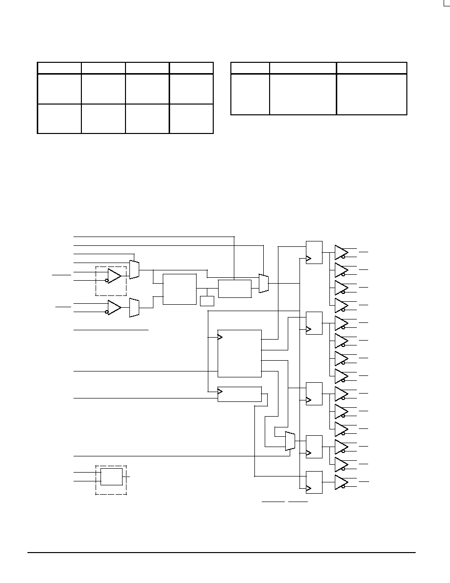
Figure 2. MPC990/991 Logic Diagram
VCO
PHASE
DETECTOR
LPF
PLL_En
VCO_Sel
ECL_Clk
ECL_Clk
Test_Clk
Ref_Sel
Ext_FB
Ext_FB
Qa0
Qa0
Qa1
Qa1
Qa2
Qa2
Qa3
Qa3
Qb0
Qb0
Qb1
Qb1
Qb2
Qb2
Qb3
Qb3
Qc0
Qc0
Qc1
Qc1
Qc2
Qc2
Qd0
Qd0
Qd1
Qd1
QFB
QFB
FREQUENCY
GENERATOR
SYNC
MR
fsela0:3
fselFB0:2
SYNC_Sel
(Pulldown)
(Pulldown)
(Pulldown)
(Pulldown)
(Pulldown)
(Pulldown)
(Pulldown)
(Pulldown)
MPC991
MPC990
Xtal
Osc
NOTE: ECL_Clk, Ext_FB have internal pulldowns, while ECL_Clk, Ext_FB have external
pullups to ensure stability under open input conditions.

MPC990 MPC991
TIMING SOLUTIONS
BR1333 -- Rev 6
5
MOTOROLA
ECL DC CHARACTERISTICS (TA = 0
∞
to 70
∞
C, VCCA = VCCI = VCCO = 0V, GNDI = ≠3.3V
±
5%, Note 1.)
0
∞
C
25
∞
C
70
∞
C
Symbol
Characteristic
Min
Typ
Max
Min
Typ
Max
Min
Typ
Max
Unit
VOH
Output HIGH Voltage
≠1.3
≠0.7
≠1.3
≠1.0
≠0.7
≠1.3
≠0.7
V
VOL
Output LOW Voltage
≠2.0
≠1.4
≠2.0
≠1.7
≠1.4
≠2.0
≠1.4
V
VIH
Input HIGH Voltage
≠1.1
≠0.9
≠1.1
≠0.9
≠1.1
≠0.9
V
VIL
Input LOW Voltage
≠1.8
≠1.5
≠1.8
≠1.5
≠1.8
≠1.5
V
VPP
Minimum Input Swing
500
500
500
mV
VCMR
Common Mode Range
VCC
≠1.3V
VCC
≠0.5V
VCC
≠1.3V
VCC
≠0.5V
VCC
≠1.3V
VCC
≠0.5V
V
IIH
Input HIGH Current
150
150
150
µ
A
IGNDI
Power Supply Current
200
240
200
240
200
240
mA
1. Refer to Motorola Application Note AN1545/D "
Thermal Data for MPC Clock Drivers" for thermal management guidelines.
PECL DC CHARACTERISTICS (TA = 0
∞
to 70
∞
C, VCCA = VCCI = VCCO = 3.3V
±
5%, GNDI = 0V, Note 2.)
0
∞
C
25
∞
C
70
∞
C
Symbol
Characteristic
Min
Typ
Max
Min
Typ
Max
Min
Typ
Max
Unit
VOH
Output HIGH Voltage (Note 3.)
2.0
2.6
2.0
2.3
2.6
2.3
2.6
V
VOL
Output LOW Voltage (Note 3.)
1.3
1.9
1.3
1.6
1.9
1.3
1.9
V
VIH
Input HIGH Voltage (Note 3.)
2.2
2.4
2.2
2.4
2.2
2.4
V
VIL
Input LOW Voltage (Note 3.)
1.5
1.8
1.5
1.8
1.5
1.8
V
VPP
Minimum Input Swing
500
500
500
mV
VCMR
Common Mode Range
VCC
≠1.3V
VCC
≠0.5V
VCC
≠1.3V
VCC
≠0.5V
VCC
≠1.3V
VCC
≠0.5V
V
IIH
Input HIGH Current
150
150
150
µ
A
IGNDI
Power Supply Current
200
240
200
240
200
240
mA
2. Refer to Motorola Application Note AN1545/D "
Thermal Data for MPC Clock Drivers" for thermal management guidelines.
3. These values are for VCC = 3.3V. Level Specifications will vary 1:1 with VCC.
AC CHARACTERISTICS (TA = 0
∞
to 70
∞
C, VCCA = VCCI = VCCO = 3.3V
±
5%, Termination of 50
to VCC ≠ 2.0V)
Symbol
Characteristic
Min
Typ
Max
Unit
Condition
fxtal
Crystal Oscillator Frequency
10
25
MHz
tr, tf
Output Rise/Fall Time
0.2
1.0
ns
20% to 80%
tpw
Output Duty Cycle
47.5
50
52.5
%
tos
Output-to-Output Skew
Same Frequency
Different Frequencies
150
250
250
350
ps
fVCO
PLL VCO Lock Range
VCO_Sel = `0'
VCO_Sel = `1'
400
200
800
400
MHz
FB
˜
8 to
˜
32 (Note 4.)
FB
˜
4 to
˜
32
tpd
Ref to Feedback Offset
75
250
425
ps
fref = 50MHz (Note 5.)
fmax
Maximum Output Frequency
Qa,Qb,Qc (
˜
2)
Qa,Qb,Qc (
˜
4)
Qa,Qb,Qc (
˜
6)
Qa,Qb,Qc (
˜
8)
400
200
133
100
MHz
tjitter
Cycle≠to≠Cycle Jitter (Peak≠to≠Peak)
±
50
ps
tlock
Maximum PLL Lock Time
10
ms
4. With VCO_Sel = `0', the PLL will be unstable with a
˜
2,
˜
4 or
˜
6 feedback ratio. With VCO_Sel = `1', the PLL will be unstable with a
˜
2 feedback
ratio.
5. tpd is specified for 50MHz input reference FB
˜
8. The window will shrink/grow proportionally from the minimum limit with shorter/longer input
reference periods. The tpd does not include jitter.