 | –≠–ª–µ–∫—Ç—Ä–æ–Ω–Ω—ã–π –∫–æ–º–ø–æ–Ω–µ–Ω—Ç: MPXY8040A | –°–∫–∞—á–∞—Ç—å:  PDF PDF  ZIP ZIP |
MPXY8000
Rev 1, 12/2004
Freescale Semiconductor
Technical Data
© Freescale Semiconductor, Inc., 2004. All rights reserved.
Tire Pressure Monitoring Sensor
Temperature Compensated
and Calibrated, Fully Integrated,
Digital Output
The Freescale Semiconductor MPXY8000 series sensor is an 8-pin tire
monitoring sensor which is comprised of a variable capacitance pressure
sensing element, a temperature sensing element, and an interface circuit (with
a wake-up feature) all on a single chip. It is housed in a Super-Small Outline
Package (SSOP), which includes a media protection filter. Specifically designed
for the low power consumption requirements of tire pressure monitoring
systems, it can combine with a Freescale Semiconductor remote keyless entry
(RKE) system to facilitate a low-cost, highly integrated system.
Detailed Description
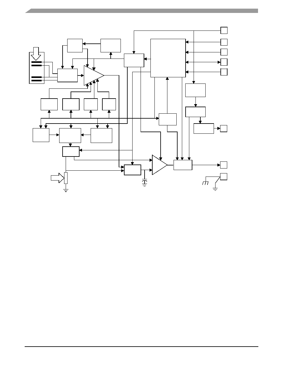
The block diagram of the MPXY8000 series sensor is shown in Figure 1. The
pressure sensor is a capacitive transducer constructed using surface
micromachining, the temperature sensor is constructed using a diffused
resistor, and the interface circuit is integrated onto the same die as the sensors
using a standard silicon CMOS process.
The conditioning of the pressure signal begins with a capacitance to voltage
conversion (C to V) followed by a switched capacitor amplifier. This amplifier
has adjustable offset and gain trimming. The offset and gain are factory
calibrated, with calibration values stored in the EEPROM trim register. This
amplifier also has temperature compensation circuits for both sensitivity and
offset, which also are factory adjusted using the EEPROM trim register.
The pressure is monitored by a voltage comparator, which compares the
measured value against an 8-bit threshold adjusted by a serial input. By
adjusting the threshold and monitoring the state of the OUT pin the external
device can check whether a low-pressure threshold has been crossed, or
perform up to 8-bit A/D conversions.
The temperature is measured by a diffused resistor with a positive
temperature coefficient driven by a current source, thereby creating a voltage.
The room temperature value of this voltage is factory calibrated using the
EEPROM trim register. A two-channel multiplexer can route either the pressure
or temperature signal to a sampling capacitor that is monitored by a voltage
comparator with variable threshold adjust, providing a digital output for
temperature.
An internal low frequency, low power 5.4 kHz oscillator with a 14-stage
divider provides a periodic pulse to the OUT pin (divide by 16384 for 3 seconds).
This pulse can be used to wake up an external MCU to begin an interface with
the device. An additional 10-stage divider will provide a pulse every 52 minutes
which can be used to reset an external MCU.
The power consumption can be controlled by several operational modes
selected by external pins.
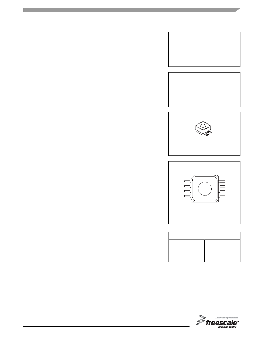
MPXY8020A
MPXY8040A
SUPER SMALL OUTLINE PACKAGE
CASE 1352-03
PIN ASSIGNMENT
TIRE PRESSURE
MONITORING SENSOR
MPXY8020A:
OPTIMIZED FOR 250 kPa ≠ 450 kPa
MPXY8040A:
OPTIMIZED FOR 500 kPa ≠ 900 kPa
S1/V
PP
1
V
DD
2
V
SS
3
OUT 4
8-pin Super Small Outline Package (SSOP)
8 SO
7 CLK
6 DATA
5 RST
ORDERING INFORMATION
Shipped In Rails
Shipped in Tape &
Reel
MPXY8020A6U
MPXY8040A6U
MPXY8020A6T1
MPXY8040A6T1
Sensor Devices
2
Freescale Semiconductor
MPXY8000
Figure 1. MPXY8000 Series Sensor Block Diagram
Operating Modes
The device has several operating modes dependent on
the applied voltages to the S1 and S0 pins as shown in
Table 1. In all the modes listed the channel multiplexers, D/A
Register, LFO, and the output pulse dividers will always be
powered up as long as there is a voltage source connected to
the V
DD
pin.
When only the S0 pin is at a logic one the pressure
measuring circuit in the device is powered up and the
pressure output signal is connected to the sample capacitor
through a multiplexer. When the S0 pin returns to the low
state the multiplexer will first turn off to store the signal on the
sample capacitor before powering down the measuring
circuitry.
When only the S1 pin is at a logic one the temperature
measuring circuit in the device is powered up and the
temperature output signal is connected to the sample
capacitor through a multiplexer. When the S1 pin returns to
the low state the multiplexer will first turn off to store the signal
on the sample capacitor before powering down the
measuring circuitry.
NOTE: All of the EEPROM trim bits will be powered up
regardless of whether the pressure or temperature
measuring circuitry is activated.
NOTE: If the voltage on the S1 pin exceeds 2.5 times the
voltage on the V
DD
pin the device will be placed into its Trim/
Test Mode.
NOTE: If the V
DD
supply source is switched off in order to
reduce current consumption, it is important that all input pins
be driven LOW to avoid powering up the device.
If any input pin (S1, S0, DATA, or CLK) is driven HIGH
while the V
DD
supply is switched off, the device may be
powered up through an ESD protection diode. In such a case,
the effective V
DD
voltage will be about 0.3 V less than the
voltage applied to the input pin, and the full device I
DD
current
will be drawn from the device driving input.
8-Bit
Current
Source
+
-
f
LF
AV
SS
AV
SS
AV
SS
Digital
Control
Power
Control
Clock
Gen
P
X
P
REF
P-Cell
C to V
Convert
AMP
f
HF
Internal HF
OSC.
P-Off
Trim
P-Gain
Trim
P-TCO
Trim
P-TCS
Trim
T-Off
Trim
2-Chan
MUX
t
PTC
Res.
2-Chan
MUX
V
DD
S1
S0
CLK
Data
RST
OUT
V
SS
COMP
3-Chan
MUX
Lock
Internal LF
OSC.
14-Stage
Divider
Sample CAP
10-Stage
Divider
8-Bit
D/A
Register
Sensor Devices
Freescale Semiconductor
3
MPXY8000
Pin Functions
The following paragraphs give a description of the general
function of each pin.
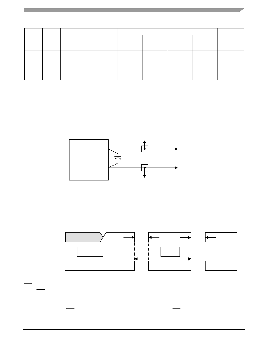
V
DD
and V
SS
Pins
Power is supplied to the control IC through V
DD
and V
SS
.
V
DD
is the positive supply and V
SS
is the digital and analog
ground. The control IC operates from a single power supply.
Therefore, the conductors to the power supply should be
connected to the V
DD
and V
SS
pins and locally decoupled as
shown in Figure 2.
Figure 2. Recommended Power Supply Connections
OUT Pin
The OUT pin normally provides a digital signal related to
the voltage applied to the voltage comparator and the
threshold level shifted into an 8-bit register from an external
device. When the device is placed in the standby mode the
OUT pin is driven high and will be clocked low when an
overflow is detected from a clock divider (divide by 16384)
driven by the LFO. This allows the OUT pin to wake up an
external device such as an MCU.
Figure 3
. Pulse on
OUT Pin During Standby Mode
RST Pin
The RST pin is normally driven high and will be clocked
low when an overflow is detected from total clock divider
(divide by 16,777,216) driven by the LFO. This allows the
RST pin to reset an external device such as an MCU. This
pulse will appear on the RST pin approximately every
52 minutes regardless of the operating mode of the device.
The pulse lasts for two cycles of the LFO oscillator as shown
in Figure 4. Since the RST pin is clocked from the same
divider string as the OUT pin, there will also be a pulse on the
OUT pin when the RST pin pulses every 52 minutes.
Table 1. Operating Modes
S1
S0
Operating Mode
Circuitry Powered
Serial Data
Counter
Pressure
Measure
System
Temp
Measure
System
A/D Output
Comp.
LFO
Oscill.
0
0
Standby/Reset
OFF
OFF
OFF
ON
ACTIVE
0
1
Measure Pressure
ON
OFF
OFF
ON
RESET
1
0
Measure Temperature
OFF
ON
OFF
ON
RESET
1
1
Output Read
OFF
OFF
ON
ON
ACTIVE
To Other V
DD
Loads
MPXY8020A
V
DD
V
SS
0.1
µF
V
DD
V
SS
To Other V
SS
Returns
To Power Supply
2/f
LFO
OUT
Operation
Wake Up
Measure
Standby
Measure
3 Sec
2/f
LFO
Sensor Devices
4
Freescale Semiconductor
MPXY8000
Figure 4. Pulse on RST Pin
S0 Pin
The S0 pin is used to select the mode of operation as
shown in Table 1.
The S0 pin contains an internal Schmitt trigger as part of
its input to improve noise immunity. The S0 pin has an
internal pull-down device in order to provide a low level when
the pin is left unconnected.
S1 Pin
The S1 pin is used to select the mode of operation, as
shown in Table 1.
The S1 pin contains an internal Schmitt trigger as part of
its input to improve noise immunity. This pin has an internal
pull-down device to provide a low level when the pin is left
unconnected.
The S1 pin also serves the purpose of enabling factory trim
and test of the device.
The higher V
PP
programming voltage for the internal
EEPROM trim register is also supplied through the S1 pin.
DATA Pin
The DATA pin is the serial data in (SDI) function for setting
the threshold of the voltage comparator.
The DATA pin contains an internal Schmitt trigger as part
of its input to improve noise immunity. This pin has an internal
pull-down device to provide a low level when the pin is left
unconnected.
CLK Pin
The CLK pin is used to provide a clock used for loading
and shifting data into the DATA pin. The data on the DATA pin
is clocked into a shift register on the rising edge of the CLK
pin signal. The data is transferred to the D/A Register on the
eighth falling edge of the CLK pin. This protocol may be
handled by the SPI or SIOP serial I/O function found on some
MCU devices.
The CLK pin contains an internal Schmitt trigger as part of
its input to improve noise immunity. The CLK pin has an
internal pull-down device to provide a low level when the pin
is left unconnected.
Output Threshold Adjust
The state of the
OUT
pin is driven by a voltage comparator
whose output state depends on the level of the input voltage
on the sample capacitor and the level of an adjustable 8-bit
threshold voltage. The threshold is adjusted by shifting data
bits into the D/A Register (DAR) via the DATA pin while
clocking the CLK pin. The timing of this data is shown in
Figure 4. Data is transferred into the serial shift register on
the rising edge of the CLK pin. On the falling edge of the 8
th
clock the data in the serial shift register is latched into the
parallel DAR register. The DAR remains powered up
whenever V
DD
is present. The serial data is clocked into the
DATA pin starting with the MSB first. This sequence of
threshold select bits is shown in Table 2.
OUT
RST
Standby
3 Sec
2/f
LFO
2/f
LFO
52 Minutes
Table 2. D/A Threshold Bit Assignment
Function
Bit Weight
Data Bit
LSB
1
D0
2
D1
4
D2
Voltage Comparator Threshold Adjust (8 bits)
8
D3
16
D4
32
D5
64
D6
MSB
128
D7
Sensor Devices
Freescale Semiconductor
5
MPXY8000
An analog to digital (A/D) conversion can be accomplished
with eight (8) different threshold levels in a successive
approximation algorithm; or the OUT pin can be set to trip at
some alarm level. The voltage on the sample capacitor will
maintain long enough for a single 8-bit conversion, but may
need to be refreshed with a new measured reading if the read
interval is longer than the specified hold time, t
SH
.
The counter that determines the number of clock pulses
into the device is reset whenever the device is placed into the
Measure Pressure or Measure Temperature Modes. This
provides a means to reset the data transfer count in case the
clock stream is corrupted during a transmission. In these two
modes the DATA and CLK pins should not be clocked to
reduce noise in the captured pressure or temperature data.
Any change in the DAR contents should be done during the
Standby or Output Read Modes.
Both the serial bit counter and the state of the DAR are
undefined following power up of the device. The serial bit
counter can be reset by cycling either the SO pin or the
S1/VPP pin to a high level and then back low. The DAR can
then be reset to the lowest level by holding the DATA pin low
while bursting the CLK pin with eight (8) clock pulses.
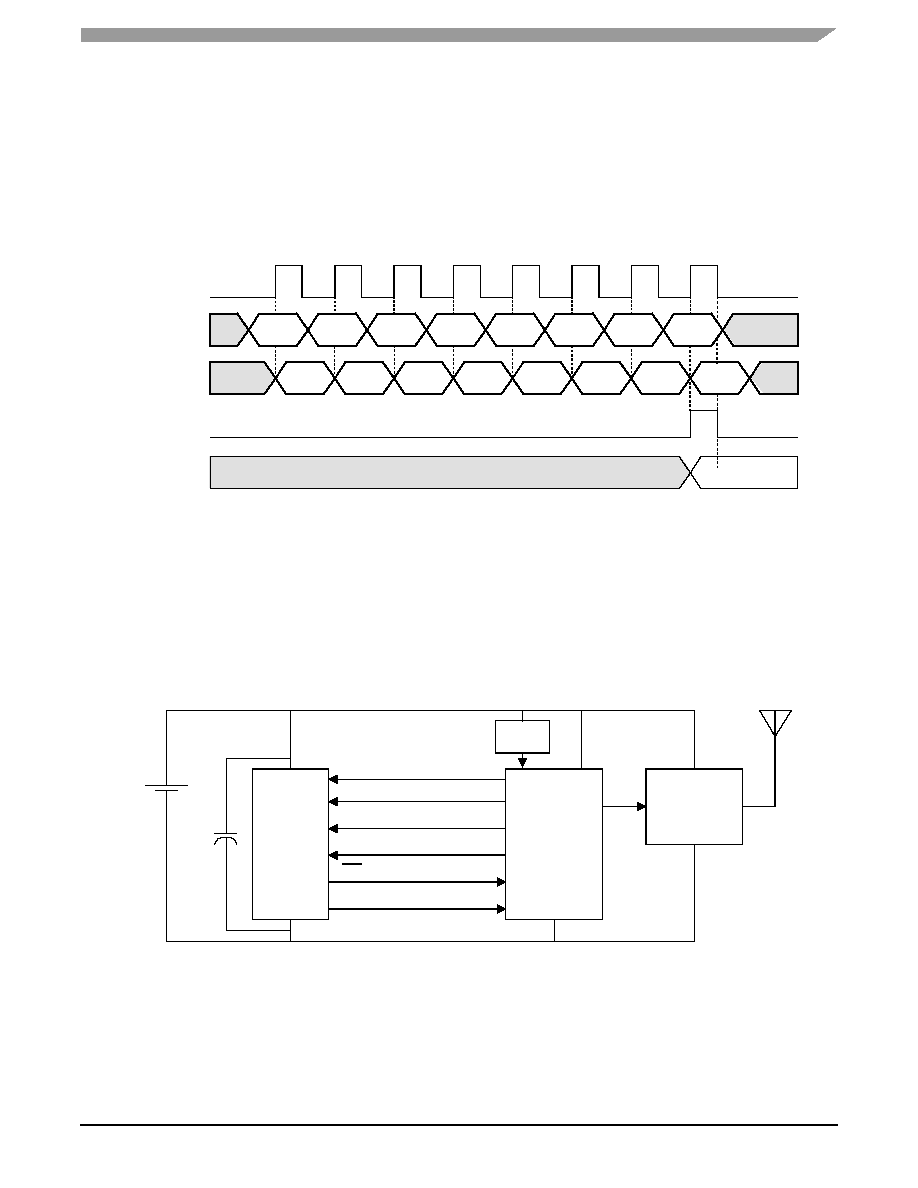
Figure 5. Serial Data Timing
Pressure Sensor Output
The pressure channel compares the output of its analog
measurement circuit to the D/A reference voltage. The device
is calibrated at two different nominal values depending on the
calibration option.
Temperature Sensor Output
The temperature channel compares the output of a
positive temperature coefficient (PTC) resistor driven by a
switched current source. The current source is only active
when the temperature channel is selected.
APPLICATIONS
Suggested application example is shown in Figure 6.
Figure 6. Application Example
CLK
Data
Serial Data
DAR Load *
DAR *
(*) Denotes Internal Signal
1
2
3
4
5
6
7
8
MSB
MSB
Data
BIT6
BIT5
BIT4
BIT3
BIT2
BIT1
LSB
BIT6
BIT5
BIT4
BIT3
BIT2
BIT1
LSB
+
3.0 V
0.1
µF
MPXY8000
Series
Sensor
V
DD
V
SS
Optional
State Machine
or MCU
RF
Transmitter
S1
S0
CLK
RST
OUT
Data
Motion
Sense