1
MRFIC1814
MOTOROLA RF DEVICE DATA
Advance Information
The MRFIC Line
1.9 GHz GaAs Downconverter
Designed primarily for use in wireless Personal Communication Systems
(PCS) applications such as Digital European Cordless Telephone (DECT),
Japan's Personal Handy System (PHS), and the emerging North American
systems. The MRFIC1814 includes a low noise amplifier and downmixer in a
low-cost TSSOP¡16 package. The integrated circuit requires minimal off-chip
matching while allowing for the maximum in flexibility and efficiency. The mixer
is optimized for low¡side injection and offers reasonable intercept point as well
as high efficiency with 9 dB of conversion gain. Image filtering is implemented
off-chip to allow maximum flexibility. CMOS compatible ENABLE pins allow
standby operation where the current drain is less than 0.1 mA.
Together with the rest of the MRFIC180X series, this GaAs IC family offers
the complete transmit and receive functions, less LO and filters, needed for a
typical 1.8 GHz cordless telephone.
╖
Usable Frequency Range = 1.8 to 2.0 GHz
╖
17 dB Typ Gain, 2.5 dB Typ Noise Figure LNA
╖
8 dB Typ Gain, 10 dB Typ Noise Figure Mixer
╖
¡5.5 dBm Typ Mixer Input Intercept Point
╖
Simple LO/IF Off-chip Matching for Maximum Flexibility
╖
Low Power Consumption = 39 mW (Typ)
╖
Single Bias Supply = 2.7 to 4.5 Volts
╖
Low LO Power Requirement = ¡ 5 dBm (Typ)
╖
Low Cost Surface Mount Plastic Package
╖
Order MRFIC1814R2 for Tape and Reel.
R2 Suffix = 2,500 Units per 16 mm, 13 inch Reel.
╖
Device Marking = M1814
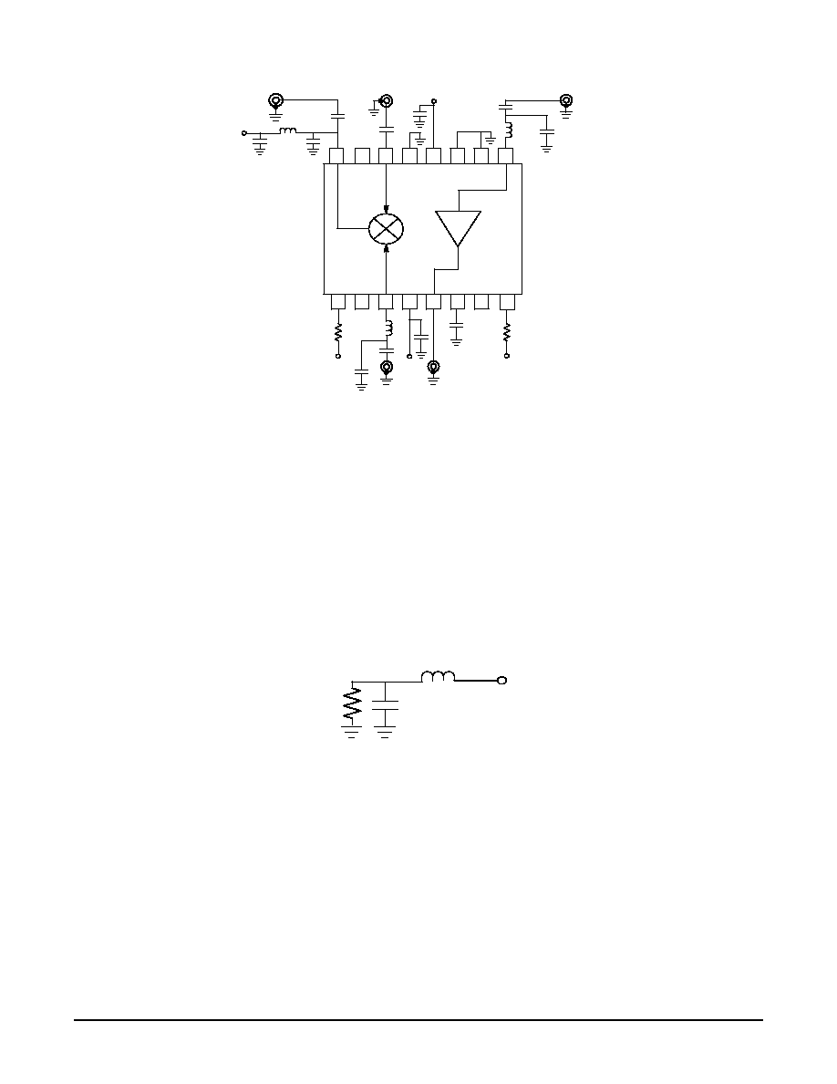
VDD2
N/C
LNA OUT
MIXER ENABLE
IF OUT/VDD3
MIXER IN
GND
GND
LNA IN
GND
VDD1
LNA
MIXER
1
2
3
4
5
6
7
8
14
13
12
11
10
9
LO INPUT
LNA CAP
LNA ENABLE
Pin Connections and Functional Block Diagram
15
16
N/C
N/C
Order this document
by MRFIC1814/D
MOTOROLA
SEMICONDUCTOR TECHNICAL DATA
1.8 GHz LOW NOISE
AMPLIFIER AND
DOWNMIXER
CASE 948C¡03
(TSSOP¡16)
MRFIC1814
⌐
Motorola, Inc. 1997

MRFIC1814
2
MOTOROLA RF DEVICE DATA
MAXIMUM RATINGS
(TA = 25
░
C unless otherwise noted)
Rating
Symbol
Limit
Unit
Supply Voltage
VDD
5.5
Vdc
LNA Input Power
LNAin
10
dBm
LO Input Power
PLO
10
dBm
Enable Voltage
ENABLE
5.5
Vdc
Storage Temperature Range
Tstg
¡ 65 to +150
░
C
Operating Ambient Temperature
TA
¡ 30 to + 85
░
C
RECOMMENDED OPERATING RANGES
Parameter
Symbol
Value
Unit
RF Input Frequency
fRF
1.8 to 2.0
GHz
Mixer LO Frequency
fLO
1.5 to 1.8
GHz
IF Output Frequency
fIF
70 to 300
MHz
Supply Voltage
VDD
2.7 to 4.5
Vdc
Enable Voltage, ON
MIXER, LNA ENABLE
2.7 to VDD
Vdc
Enable Voltage, OFF
MIXER, LNA ENABLE
0 to 0.2
Vdc
ELECTRICAL CHARACTERISTICS
(VDD = 3 V, TA = 25
░
C, LO = 1.65 GHz @ ¡ 5 dBm, RF = 1.9 GHz @ ¡30 dBm, MIXER & LNA
ENABLE = 3 V)
Characteristic
Min
Typ
Max
Unit
LNA Gain (LNA ENABLE = 3 V)
14
17
--
dB
LNA Gain (LNA ENABLE = 0 V)
--
¡19
--
dB
LNA Noise Figure
--
2.5
--
dB
LNA Input 3rd Order Intercept
--
¡7
--
dBm
LNA Output 1 dB Gain Compression Point
¡6
¡3
--
dBm
Mixer Conversion Gain (into 50
)
5
8
--
dB
Mixer Noise Figure
--
10
--
dB
Mixer Input 3rd Order Intercept
--
¡5
--
dBm
Mixer Output 1 dB Gain Compression Point
¡8.5
¡5.5
--
dBm
Total Supply Current (ENABLE VOLTAGES = 3.0 V, LO off)
--
10
17
mA
Total Supply Current (ENABLE VOLTAGES = 3.0 V, LO on)
--
13
--
mA
Standby Mode Current (ENABLE VOLTAGES = 0 V, LO off)
--
0.05
0.25
mA

MRFIC1814
4
MOTOROLA RF DEVICE DATA
PACKAGE DIMENSIONS
A
B
PIN 1
IDENTIFICATION
L
1
8
9
16
D
C
SEATING
G
H
F
M
DIM
A
MIN
MAX
MIN
MAX
INCHES
¡¡¡
5.10
¡¡¡
0.200
MILLIMETERS
B
4.30
4.50
0.169
0.177
C
¡¡¡
1.20
¡¡¡
0047
D
0.05
0.25
0.002
0.010
F
0.45
0.55
0.018
0.022
G
0.65 BSC
0.026 BSC
H
0.22
0.23
0.009
0.010
J
0.09
0.24
0.004
0.009
K
0.16
0.32
0.006
0.013
L
6.30
6.50
0.248
0.256
M
0
10
0
10
NOTES:
1.
DIMENSIONING AND TOLERANCING PER ANSI
Y14.5M, 1982.
2.
CONTROLLING DIMENSION: MILLIMETER.
3.
DIMENSION A DOES NOT INCLUDE MOLD
FLASH, PROTRUSIONS OR GATE BURRS. MOLD
FLASH OR GATE BURRS SHALL NOT EXCEED
0.15 (0.006) PER SIDE.
4.
DIMENSION B DOES NOT INCLUDE
INTERLEAD FLASH OR PROTRUSION.
INTERLEAD FLASH OR PROTRUSION SHALL NOT
EXCEED 0.25 (0.010) PER SIDE.
5.
DIMENSION K DOES NOT INCLUDE DAMBAR
PROTRUSION. ALLOWABLE DAMBAR
PROTRUSION SHALL BE 0.08 (0.003) TOTAL
EXCESS OF THE K DIMENSION AT MAXIMUM
MATERIAL CONDITION.
6.
TERMINAL NUMBERS ARE SHOWN FOR
REFERENCE ONLY.
7.
DIMENSIONS A AND B ARE TO BE
DETERMINED AT DATUM PLANE ¡U¡.
░
░
░
░
J1
0.09
0.18
0.004
0.007
K1
0.16
0.26
0.006
0.010
K
K1
J
J1
SECTION A¡A
A
A
16x REF
K
0.100 (0.004)
M
-T-
0.200 (0.008)
M
T
-U-
-P-
PLANE
CASE 948C¡03
ISSUE B
Motorola reserves the right to make changes without further notice to any products herein. Motorola makes no warranty, representation or guarantee regarding
the suitability of its products for any particular purpose, nor does Motorola assume any liability arising out of the application or use of any product or circuit, and
specifically disclaims any and all liability, including without limitation consequential or incidental damages. "Typical" parameters which may be provided in Motorola
data sheets and/or specifications can and do vary in different applications and actual performance may vary over time. All operating parameters, including "Typicals"
must be validated for each customer application by customer's technical experts. Motorola does not convey any license under its patent rights nor the rights of
others. Motorola products are not designed, intended, or authorized for use as components in systems intended for surgical implant into the body, or other
applications intended to support or sustain life, or for any other application in which the failure of the Motorola product could create a situation where personal injury
or death may occur. Should Buyer purchase or use Motorola products for any such unintended or unauthorized application, Buyer shall indemnify and hold Motorola
and its officers, employees, subsidiaries, affiliates, and distributors harmless against all claims, costs, damages, and expenses, and reasonable attorney fees
arising out of, directly or indirectly, any claim of personal injury or death associated with such unintended or unauthorized use, even if such claim alleges that
Motorola was negligent regarding the design or manufacture of the part. Motorola and are registered trademarks of Motorola, Inc. Motorola, Inc. is an Equal
Opportunity/Affirmative Action Employer.
Mfax is a trademark of Motorola, Inc.
How to reach us:
USA / EUROPE / Locations Not Listed: Motorola Literature Distribution;
JAPAN: Nippon Motorola Ltd.: SPD, Strategic Planning Office, 4¡32¡1,
P.O. Box 5405, Denver, Colorado 80217. 1¡303¡675¡2140 or 1¡800¡441¡2447
Nishi¡Gotanda, Shinagawa¡ku, Tokyo 141, Japan. 81¡3¡5487¡8488
Customer Focus Center: 1¡800¡521¡6274
Mfax
TM
: RMFAX0@email.sps.mot.com ¡ TOUCHTONE 1¡602¡244¡6609
ASIA/PACIFIC: Motorola Semiconductors H.K. Ltd.; 8B Tai Ping Industrial Park,
Motorola Fax Back System
¡ US & Canada ONLY 1¡800¡774¡1848
51 Ting Kok Road, Tai Po, N.T., Hong Kong. 852¡26629298
¡ http://sps.motorola.com/mfax/
HOME PAGE: http://motorola.com/sps/
MRFIC1814/D