1
Motorola TMOS Power MOSFET Transistor Device Data
Designer's
TM
Data Sheet
ISOTOP
TM
TMOS E-FET
.
TM
Power Field Effect Transistor
NÙChannel EnhancementÙMode Silicon Gate
This advanced high voltage TMOS EÙFET is designed to
withstand high energy in the avalanche mode and switch efficiently.
This new high energy device also offers a drainÙtoÙsource diode
with fast recovery time. Designed for high voltage, high speed
switching applications such as power supplies, PWM motor
controls and other inductive loads, the avalanche energy capability
is specified to eliminate the guesswork in designs where inductive
loads are switched and offer additional safety margin against
unexpected voltage transients.
ñ
2500 V RMS Isolated Isotop Package
ñ
Avalanche Energy Specified
ñ
SourceÙtoÙDrain Diode Recovery Time Comparable to a Discrete
Fast Recovery Diode
ñ
Diode is Characterized for Use in Bridge Circuits
ñ
Very Low Internal Parasitic Inductance
ñ
IDSS and VDS(on) Specified at Elevated Temperature
ñ
U. L. Recognized, File #E69369
MAXIMUM RATINGS
(TC = 25
¯
C unless otherwise noted)
Rating
Symbol
Value
Unit
DrainÙSource Voltage
VDSS
100
Vdc
DrainÙGate Voltage (RGS = 1.0 M
)
VDGR
100
Vdc
GateÙSource Voltage -- Continuous
GateÙSource Voltage
-- NonÙRepetitive (tp
10 ms)
VGS
VGSM
Ý
20
Ý
40
Vdc
Vpk
Drain Current -- Continuous
Drain Current
-- Continuous @ 100
¯
C
Drain Current
-- Single Pulse (tp
10
ç
s)
ID
ID
IDM
215
136
860
Adc
Total Power Dissipation
Derate above 25
¯
C
PD
460
3.70
Watts
W/
¯
C
Operating and Storage Temperature Range
TJ, Tstg
Ù 40 to 150
¯
C
Single Pulse DrainÙtoÙSource Avalanche Energy
(VDD = 25 Vdc, VGS = 10 Vdc, IL = 215 Apk, L = 0.017 mH, RG = 25
,
)
EAS
400
mJ
RMS Isolation Voltage
VISO
2500
Vac
Thermal Resistance -- Junction to Case
Thermal Resistance
-- Junction to Ambient
R
JC
R
JA
0.28
62.5
¯
C/W
Maximum Lead Temperature for Soldering Purposes, 1/8
from case for 10 seconds
TL
260
¯
C
Designer's Data for "Worst Case" Conditions -- The Designer's Data Sheet permits the design of most circuits entirely from the information presented. SOA Limit
curves -- representing boundaries on device characteristics -- are given to facilitate "worst case" design.
EÙFET is a trademark of Motorola, Inc. TMOS is a registered trademark of Motorola, Inc.
ISOTOP is a trademark of SGSÙTHOMSON Microelectronics.
Preferred devices are Motorola recommended choices for future use and best overall value.
REV 1
Order this document
by MTE215N10E/D
MOTOROLA
SEMICONDUCTOR TECHNICAL DATA
MTE215N10E
TMOS POWER FET
215 AMPERES
100 VOLTS
RDS(on) = 0.0055 OHM
Motorola Preferred Device
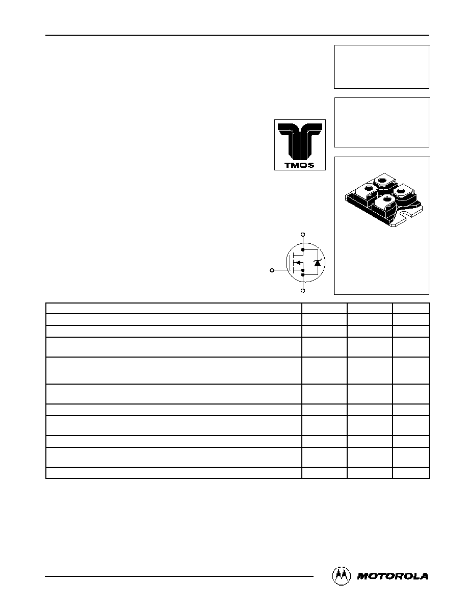
D
S
G
Û
SOTÙ227B
1
2
3
4
1. Source
2. Gate
3. Drain
4. Source 2
ˋ
Motorola, Inc. 1995

MTE215N10E
2
Motorola TMOS Power MOSFET Transistor Device Data
ELECTRICAL CHARACTERISTICS
(TJ = 25
¯
C unless otherwise noted)
Characteristic
Symbol
Min
Typ
Max
Unit
OFF CHARACTERISTICS
DrainÙSource Breakdown Voltage
(VGS = 0 Vdc, ID = 250
ç
Adc)
Temperature Coefficient (Positive)
V(BR)DSS
100
--
110
120
--
--
Vdc
mV/
¯
C
Zero Gate Voltage Drain Current
(VDS = 100 Vdc, VGS = 0 Vdc)
(VDS = 100 Vdc, VGS = 0 Vdc, TJ = 125
¯
C)
IDSS
--
--
--
--
10
100
ç
Adc
GateÙBody Leakage Current (VGS =
Ý
20 Vdc, VDS = 0)
IGSS
--
--
200
nAdc
ON CHARACTERISTICS (1)
Gate Threshold Voltage
(VDS = VGS, ID = 250
ç
Adc)
Threshold Temperature Coefficient (Negative)
VGS(th)
2.0
--
3.0
--
4.0
--
Vdc
mV/
¯
C
Static DrainÙSource OnÙResistance (VGS = 10 Vdc, ID = 107.5 Adc)
RDS(on)
--
4.6
5.5
mOhm
DrainÙSource OnÙVoltage (VGS = Vdc)
(ID = 215 Adc)
(ID = 107.5 Adc, TJ = 125
¯
C)
VDS(on)
--
--
--
--
1.5
1.2
Vdc
Forward Transconductance (VDS = 15 Vdc, ID = 107.5 Adc)
gFS
100
140
--
mhos
DYNAMIC CHARACTERISTICS
Input Capacitance
(VDS = 25 Vdc, VGS = 0 Vdc,
f = 1.0 MHz)
Ciss
--
15200
--
pF
Output Capacitance
(VDS = 25 Vdc, VGS = 0 Vdc,
f = 1.0 MHz)
Coss
--
6600
--
Reverse Transfer Capacitance
f = 1.0 MHz)
Crss
--
2400
--
SWITCHING CHARACTERISTICS (2)
TurnÙOn Delay Time
(VDD = 50 Vdc, ID = 215 Adc,
VGS = 10 Vdc,
RG = 5.0
)
td(on)
--
48
--
ns
Rise Time
(VDD = 50 Vdc, ID = 215 Adc,
VGS = 10 Vdc,
RG = 5.0
)
tr
--
490
--
TurnÙOff Delay Time
VGS = 10 Vdc,
RG = 5.0
)
td(off)
--
186
--
Fall Time
G = 5.0
)
tf
--
384
--
Gate Charge
(VDS = 80 Vdc, ID = 215 Adc,
VGS =10 Vdc)
QT
--
540
--
nC
(VDS = 80 Vdc, ID = 215 Adc,
VGS =10 Vdc)
Q1
--
104
--
(VDS = 80 Vdc, ID = 215 Adc,
VGS =10 Vdc)
Q2
--
300
--
Q3
--
440
--
SOURCEÙDRAIN DIODE CHARACTERISTICS
Forward OnÙVoltage (1)
(IS = 215 Adc, VGS = 0 Vdc)
(IS = 215 Adc, VGS = 0 Vdc, TJ = 125
¯
C)
VSD
--
--
1.0
1.2
1.5
--
Vdc
Reverse Recovery Time
(IS = 215 Adc, VGS = 0 Vdc,
dIS/dt = 100 A/
ç
s)
trr
--
145
--
ns
(IS = 215 Adc, VGS = 0 Vdc,
dIS/dt = 100 A/
ç
s)
ta
--
90
--
(IS = 215 Adc, VGS = 0 Vdc,
dIS/dt = 100 A/
ç
s)
tb
--
55
--
Reverse Recovery Stored Charge
QRR
--
4.6
--
ç
C
INTERNAL PACKAGE INDUCTANCE
Internal Drain Inductance
(Measured from contact screw on tab to center of die)
(Measured from the drain lead 0.25
from package to center of die)
LD
--
--
3.5
5.0
--
--
nH
Internal Source Inductance
(Measured from the source lead 0.25
from package to source pad)
LS
--
5.0
--
nH
(1) Pulse Test: Pulse Width
300
ç
s, Duty Cycle
2%.
(2) Switching characteristics are independent of operating junction temperature.

MTE215N10E
3
Motorola TMOS Power MOSFET Transistor Device Data
TYPICAL ELECTRICAL CHARACTERISTICS
R
DS(on)
, DRAINÙT
OÙSOURCE RESIST
ANCE
(NORMALIZED)
R
DS(on)
, DRAINÙT
OÙSOURCE RESIST
ANCE (OHMS)
0
VDS, DRAINÙTOÙSOURCE VOLTAGE (VOLTS)
Figure 1. OnÙRegion Characteristics
I D
, DRAIN CURRENT
(AMPS)
I D
, DRAIN CURRENT
(AMPS)
VGS, GATEÙTOÙSOURCE VOLTAGE (VOLTS)
Figure 2. Transfer Characteristics
ID, DRAIN CURRENT (AMPS)
Figure 3. OnÙResistance versus Drain Current
and Temperature
ID, DRAIN CURRENT (AMPS)
Figure 4. OnÙResistance versus Drain Current
and Gate Voltage
TJ, JUNCTION TEMPERATURE (
¯
C)
Figure 5. OnÙResistance Variation with
Temperature
VDS, DRAINÙTOÙSOURCE VOLTAGE (VOLTS)
Figure 6. DrainÙToÙSource Leakage Current
versus Voltage
TJ = 25
¯
C
VGS = 10 V
VGS = 10 V
ID = 107.5 A
7 V
6 V
Ù 50
0
50
100
150
220
165
110
55
0
4
3.5
3
2
1
240
160
120
0
8
6
4
2
1
200
80
150
100
50
0
200
250
7
0
20
60
40
80
100
5 V
4 V
125
0.5
1.5
2.5
9 V
8 V
40
3
5
VDS
5 V
100
¯
C
25
¯
C
TJ = Ù 55
¯
C
0.018
0.016
0.014
0.012
0.01
0.008
0.006
0.004
0
50
100
150
200
250
TJ = 100
¯
C
25
¯
C
Ù 55
¯
C
0.016
0.014
0.012
0.01
0.008
0.006
VGS = 10 V
TJ = 25
¯
C
VGS = 10 V
15 V
R
DS(on)
, DRAINÙT
OÙSOURCE RESIST
ANCE (OHMS)
Ù 25
25
75
1.6
1.4
1.2
1
0.8
0.6
I DSS
, LEAKAGE (nA)
100000
10000
1000
100
10
1
VGS = 0 V
TJ = 125
¯
C
100
¯
C
25
¯
C

MTE215N10E
4
Motorola TMOS Power MOSFET Transistor Device Data
POWER MOSFET SWITCHING
Switching behavior is most easily modeled and predicted
by recognizing that the power MOSFET is charge controlled.
The lengths of various switching intervals (
t) are deter-
mined by how fast the FET input capacitance can be charged
by current from the generator.
The published capacitance data is difficult to use for calculat-
ing rise and fall because drainÙgate capacitance varies
greatly with applied voltage. Accordingly, gate charge data is
used. In most cases, a satisfactory estimate of average input
current (IG(AV)) can be made from a rudimentary analysis of
the drive circuit so that
t = Q/IG(AV)
During the rise and fall time interval when switching a resis-
tive load, VGS remains virtually constant at a level known as
the plateau voltage, VSGP. Therefore, rise and fall times may
be approximated by the following:
tr = Q2 x RG/(VGG Ù VGSP)
tf = Q2 x RG/VGSP
where
VGG = the gate drive voltage, which varies from zero to VGG
RG = the gate drive resistance
and Q2 and VGSP are read from the gate charge curve.
During the turnÙon and turnÙoff delay times, gate current is
not constant. The simplest calculation uses appropriate val-
ues from the capacitance curves in a standard equation for
voltage change in an RC network. The equations are:
td(on) = RG Ciss In [VGG/(VGG Ù VGSP)]
td(off) = RG Ciss In (VGG/VGSP)
The capacitance (Ciss) is read from the capacitance curve at
a voltage corresponding to the offÙstate condition when cal-
culating td(on) and is read at a voltage corresponding to the
onÙstate when calculating td(off).
At high switching speeds, parasitic circuit elements com-
plicate the analysis. The inductance of the MOSFET source
lead, inside the package and in the circuit wiring which is
common to both the drain and gate current paths, produces a
voltage at the source which reduces the gate drive current.
The voltage is determined by Ldi/dt, but since di/dt is a func-
tion of drain current, the mathematical solution is complex.
The MOSFET output capacitance also complicates the
mathematics. And finally, MOSFETs have finite internal gate
resistance which effectively adds to the resistance of the
driving source, but the internal resistance is difficult to mea-
sure and, consequently, is not specified.
The resistive switching time variation versus gate resis-
tance (Figure 9) shows how typical switching performance is
affected by the parasitic circuit elements. If the parasitics
were not present, the slope of the curves would maintain a
value of unity regardless of the switching speed. The circuit
used to obtain the data is constructed to minimize common
inductance in the drain and gate circuit loops and is believed
readily achievable with board mounted components. Most
power electronic loads are inductive; the data in the figure is
taken with a resistive load, which approximates an optimally
snubbed inductive load. Power MOSFETs may be safely op-
erated into an inductive load; however, snubbing reduces
switching losses.
GATEÙTOÙSOURCE OR DRAINÙTOÙSOURCE VOLTAGE (VOLTS)
C, CAP
ACIT
ANCE (pF)
Figure 7. Capacitance Variation
60000
0
VGS
VDS
5
0
5
10
15
20
25
10
50000
40000
30000
20000
10000
VGS = 0 V
VDS = 0 V
TJ = 25
¯
C
Crss
Coss
Ciss
Ciss
Crss

MTE215N10E
5
Motorola TMOS Power MOSFET Transistor Device Data
Qg, TOTAL GATE CHARGE (nC)
800
Figure 8. GateÙToÙSource and
DrainÙToÙSource Voltage versus Total Charge
RG, GATE RESISTANCE (OHMS)
1
10
100
1000
10
t,
TIME (ns)
VDD = 50 V
ID = 215 A
VGS = 10 V
TJ = 25
¯
C
tr
tf
td(off)
td(on)
Figure 9. Resistive Switching Time
Variation versus Gate Resistance
V
GS
, GA
TEÙT
OÙSOURCE VOL
T
AGE (VOL
TS)
0
10
8
4
0
12
1200
ID = 215 A
TJ = 25
¯
C
200
400
600
100
V
DS
, DRAINÙT
OÙSOURCE VOL
T
AGE (VOL
TS)
6
2
1000
QT
Q1
Q2
Q3
VGS
VDS
120
100
80
60
40
20
0
SAFE OPERATING AREA
The Forward Biased Safe Operating Area curves define
the maximum simultaneous drainÙtoÙsource voltage and
drain current that a transistor can handle safely when it is for-
ward biased. Curves are based upon maximum peak junc-
tion temperature and a case temperature (TC) of 25
¯
C. Peak
repetitive pulsed power limits are determined by using the
thermal response data in conjunction with the procedures
discussed in AN569, "Transient Thermal ResistanceÙGeneral
Data and Its Use."
Switching between the offÙstate and the onÙstate may tra-
verse any load line provided neither rated peak current (IDM)
nor rated voltage (VDSS) is exceeded and the transition time
(tr,tf) do not exceed 10
ç
s. In addition the total power aver-
aged over a complete switching cycle must not exceed
(TJ(MAX) Ù TC)/(R
JC).
A Power MOSFET designated EÙFET can be safely used
in switching circuits with unclamped inductive loads. For reli-
able operation, the stored energy from circuit inductance dis-
sipated in the transistor while in avalanche must be less than
the rated limit and adjusted for operating conditions differing
from those specified. Although industry practice is to rate in
terms of energy, avalanche energy capability is not a con-
stant. The energy rating decreases nonÙlinearly with an in-
crease of peak current in avalanche and peak junction
temperature.
VSD, SOURCEÙTOÙDRAIN VOLTAGE (VOLTS)
Figure 10. Diode Forward Voltage versus Current
I S
, SOURCE CURRENT
(AMPS)
VGS = 0 V
TJ = 25
¯
C
220
200
180
160
140
120
100
80
60
40
20
0
1.7
1.5
1.3
1.1
0.9
0.7
0.5