Data Sheet
C-5e NETWORK PROCESSOR
SILICON REVISION A1
C5ENPA1-DS/D
Rev 03 PRELIMINARY

Data Sheet
C-5e Network Processor
Silicon Revision A1
C5ENPA1-DS/D
Rev 03
P
r e
l i
m
i n
a r
y

Copyright � 2002 Motorola, Inc. All rights reserved. No part of this documentation may
be reproduced in any form or by any means or used to make any derivative work (such as
translation, transformation, or adaptation) without written permission from Motorola.
Motorola reserves the right to revise this documentation and to make changes in content
from time to time without obligation on the part of Motorola to provide notification of
such revision or change.
Motorola provides this documentation without warranty, term, or condition of any kind,
either implied or expressed, including, but not limited to, the implied warranties, terms or
conditions of merchantability, satisfactory quality, and fitness for a particular purpose.
Motorola may make improvements or changes in the product(s) and/or the program(s)
described in this documentation at any time.
C-5e, C-3e, C-5, Q-5, Q-3, C-Port, and C-Ware are all trademarks of C-Port, a Motorola
Company. Motorola and the stylized Motorola logo are registered in the US Patent &
Trademark Office. All other product or service names are the property of their respective
owners.

MOTOROLA GENERAL BUSINESS INFORMATION
C5ENPA1-DS/D REV 03
C5ENPA1-DS/D
Rev 03
CONTENTS
About This Guide
Guide Overview . . . . . . . . . . . . . . . . . . . . . . . . . . . . . . . . . . . . . . . . . . . . . . . . . . . . . . . . . . . . . . . . . . .
13
Data Sheet Classifications . . . . . . . . . . . . . . . . . . . . . . . . . . . . . . . . . . . . . . . . . . . . . . . . . . . . . . . . . . .
14
Using PDF Documents . . . . . . . . . . . . . . . . . . . . . . . . . . . . . . . . . . . . . . . . . . . . . . . . . . . . . . . . . . . . . .
14
Guide Conventions . . . . . . . . . . . . . . . . . . . . . . . . . . . . . . . . . . . . . . . . . . . . . . . . . . . . . . . . . . . . . . . . .
16
Revision History . . . . . . . . . . . . . . . . . . . . . . . . . . . . . . . . . . . . . . . . . . . . . . . . . . . . . . . . . . . . . . . . . . .
16
Related Product Documentation . . . . . . . . . . . . . . . . . . . . . . . . . . . . . . . . . . . . . . . . . . . . . . . . . . . . . . .
17
C
HAPTER
1
Functional Description
Features . . . . . . . . . . . . . . . . . . . . . . . . . . . . . . . . . . . . . . . . . . . . . . . . . . . . . . . . . . . . . . . . . . . . . . . . .
19
Massive Processing Power . . . . . . . . . . . . . . . . . . . . . . . . . . . . . . . . . . . . . . . . . . . . . . . . . . . . . . .
19
High Functional Integration . . . . . . . . . . . . . . . . . . . . . . . . . . . . . . . . . . . . . . . . . . . . . . . . . . . . . .
19
Block Diagram . . . . . . . . . . . . . . . . . . . . . . . . . . . . . . . . . . . . . . . . . . . . . . . . . . . . . . . . . . . . . . . . . . . .
20
Channel Processors . . . . . . . . . . . . . . . . . . . . . . . . . . . . . . . . . . . . . . . . . . . . . . . . . . . . . . . . . . . . . . . .
22
Executive Processor . . . . . . . . . . . . . . . . . . . . . . . . . . . . . . . . . . . . . . . . . . . . . . . . . . . . . . . . . . . . . . . .
23
System Interfaces . . . . . . . . . . . . . . . . . . . . . . . . . . . . . . . . . . . . . . . . . . . . . . . . . . . . . . . . . . . . .
23
Fabric Processor . . . . . . . . . . . . . . . . . . . . . . . . . . . . . . . . . . . . . . . . . . . . . . . . . . . . . . . . . . . . . . . . . . .
24
Buffer Management Unit . . . . . . . . . . . . . . . . . . . . . . . . . . . . . . . . . . . . . . . . . . . . . . . . . . . . . . . . . . . .
24
Table Lookup Unit . . . . . . . . . . . . . . . . . . . . . . . . . . . . . . . . . . . . . . . . . . . . . . . . . . . . . . . . . . . . . . . . . .
25
Queue Management Unit . . . . . . . . . . . . . . . . . . . . . . . . . . . . . . . . . . . . . . . . . . . . . . . . . . . . . . . . . . . .
26
C
HAPTER
2
Signal Descriptions
Signal Summary . . . . . . . . . . . . . . . . . . . . . . . . . . . . . . . . . . . . . . . . . . . . . . . . . . . . . . . . . . . . . . . . . . .
27
Pinout Diagram . . . . . . . . . . . . . . . . . . . . . . . . . . . . . . . . . . . . . . . . . . . . . . . . . . . . . . . . . . . . . . . . . . .
28
Pin Descriptions Grouped by Function . . . . . . . . . . . . . . . . . . . . . . . . . . . . . . . . . . . . . . . . . . . . . . . . . .
30
LVTTL and LVPECL Specifications . . . . . . . . . . . . . . . . . . . . . . . . . . . . . . . . . . . . . . . . . . . . . . . . .
30
Clock Signals . . . . . . . . . . . . . . . . . . . . . . . . . . . . . . . . . . . . . . . . . . . . . . . . . . . . . . . . . . . . . . . . .
31
CP Interface Signals . . . . . . . . . . . . . . . . . . . . . . . . . . . . . . . . . . . . . . . . . . . . . . . . . . . . . . . . . . .
32
DS1/T1 Framer Interface Configuration . . . . . . . . . . . . . . . . . . . . . . . . . . . . . . . . . . . . . . . . .
34
10/100 Ethernet (RMII) Configuration . . . . . . . . . . . . . . . . . . . . . . . . . . . . . . . . . . . . . . . . . .
34
Gigabit Ethernet (GMII) Configuration . . . . . . . . . . . . . . . . . . . . . . . . . . . . . . . . . . . . . . . . . .
35

6
CONTENTS
C5ENPA1-DS/D REV 03
MOTOROLA GENERAL BUSINESS INFORMATION
Gigabit Ethernet and Fibre Channel TBI Configuration . . . . . . . . . . . . . . . . . . . . . . . . . . . . .
38
SONET OC-3 Transceiver Interface Configuration . . . . . . . . . . . . . . . . . . . . . . . . . . . . . . . .
39
SONET OC-12 Transceiver Interface Configuration . . . . . . . . . . . . . . . . . . . . . . . . . . . . . . .
40
Executive Processor System Interface Signals . . . . . . . . . . . . . . . . . . . . . . . . . . . . . . . . . . . . . . .
42
PCI Signals . . . . . . . . . . . . . . . . . . . . . . . . . . . . . . . . . . . . . . . . . . . . . . . . . . . . . . . . . . . . . . .
42
Serial Interface Signals . . . . . . . . . . . . . . . . . . . . . . . . . . . . . . . . . . . . . . . . . . . . . . . . . . . . .
43
PROM Interface Signals . . . . . . . . . . . . . . . . . . . . . . . . . . . . . . . . . . . . . . . . . . . . . . . . . . . .
44
General System Interface Signal . . . . . . . . . . . . . . . . . . . . . . . . . . . . . . . . . . . . . . . . . . . . . .
47
Fabric Processor Interface Signals . . . . . . . . . . . . . . . . . . . . . . . . . . . . . . . . . . . . . . . . . . . . . . . .
48
BMU SDRAM Interface Signals . . . . . . . . . . . . . . . . . . . . . . . . . . . . . . . . . . . . . . . . . . . . . . . . . .
52
TLU SRAM Interface Signals . . . . . . . . . . . . . . . . . . . . . . . . . . . . . . . . . . . . . . . . . . . . . . . . . . . . .
54
QMU SRAM (Internal Mode) Interface Signals . . . . . . . . . . . . . . . . . . . . . . . . . . . . . . . . . . . . . . .
55
QMU to Q-5 TMC (External Mode) Interface Signals . . . . . . . . . . . . . . . . . . . . . . . . . . . . . . . . . .
56
Power Supply Signals . . . . . . . . . . . . . . . . . . . . . . . . . . . . . . . . . . . . . . . . . . . . . . . . . . . . . . . . . .
57
Test Signals . . . . . . . . . . . . . . . . . . . . . . . . . . . . . . . . . . . . . . . . . . . . . . . . . . . . . . . . . . . . . . . . . .
58
No Connection Pins . . . . . . . . . . . . . . . . . . . . . . . . . . . . . . . . . . . . . . . . . . . . . . . . . . . . . . . . . . . . .
58
Signals Grouped by Pin Number . . . . . . . . . . . . . . . . . . . . . . . . . . . . . . . . . . . . . . . . . . . . . . . . . . . . . .
59
JTAG Support . . . . . . . . . . . . . . . . . . . . . . . . . . . . . . . . . . . . . . . . . . . . . . . . . . . . . . . . . . . . . . . . . . . . .
69
Pinout . . . . . . . . . . . . . . . . . . . . . . . . . . . . . . . . . . . . . . . . . . . . . . . . . . . . . . . . . . . . . . . . . . . . . . .
69
JTAG Data Registers . . . . . . . . . . . . . . . . . . . . . . . . . . . . . . . . . . . . . . . . . . . . . . . . . . . . . . . . . . .
69
Boundary Scan Restriction . . . . . . . . . . . . . . . . . . . . . . . . . . . . . . . . . . . . . . . . . . . . . . . . . . . . . . .
69
Boundary Scan Cell Types . . . . . . . . . . . . . . . . . . . . . . . . . . . . . . . . . . . . . . . . . . . . . . . . . . . . . . .
69
IDcode Register . . . . . . . . . . . . . . . . . . . . . . . . . . . . . . . . . . . . . . . . . . . . . . . . . . . . . . . . . . . . . . .
71
JTAG Instruction Register . . . . . . . . . . . . . . . . . . . . . . . . . . . . . . . . . . . . . . . . . . . . . . . . . . . . . . .
71
Boundary Scan Description Language . . . . . . . . . . . . . . . . . . . . . . . . . . . . . . . . . . . . . . . . . . . . . .
72
C
HAPTER
3
Electrical Specifications
Absolute Maximum Ratings . . . . . . . . . . . . . . . . . . . . . . . . . . . . . . . . . . . . . . . . . . . . . . . . . . . . . . . . .
73
Recommended Operating Conditions . . . . . . . . . . . . . . . . . . . . . . . . . . . . . . . . . . . . . . . . . . . . . . . . . .
74
DC Characteristics . . . . . . . . . . . . . . . . . . . . . . . . . . . . . . . . . . . . . . . . . . . . . . . . . . . . . . . . . . . . . . . . .
75
Power Sequencing . . . . . . . . . . . . . . . . . . . . . . . . . . . . . . . . . . . . . . . . . . . . . . . . . . . . . . . . . . . . . . . . .
76
Power and Thermal Characteristics . . . . . . . . . . . . . . . . . . . . . . . . . . . . . . . . . . . . . . . . . . . . . . . . . . . .
77
Thermal Management Information . . . . . . . . . . . . . . . . . . . . . . . . . . . . . . . . . . . . . . . . . . . . . . . .
77
Internal Package Conduction Resistance . . . . . . . . . . . . . . . . . . . . . . . . . . . . . . . . . . . . . . . .
78
Heat Sink Selection Example . . . . . . . . . . . . . . . . . . . . . . . . . . . . . . . . . . . . . . . . . . . . . . . . .
79
AC Timing Specifications . . . . . . . . . . . . . . . . . . . . . . . . . . . . . . . . . . . . . . . . . . . . . . . . . . . . . . . . . . . .
81
Clock Timing Specifications . . . . . . . . . . . . . . . . . . . . . . . . . . . . . . . . . . . . . . . . . . . . . . . . . . . . .
82

CONTENTS
7
MOTOROLA GENERAL BUSINESS INFORMATION
C5ENPA1-DS/D REV 03
CP Timing Specifications . . . . . . . . . . . . . . . . . . . . . . . . . . . . . . . . . . . . . . . . . . . . . . . . . . . . . . . .
83
DS1/DS3 Timing Specifications . . . . . . . . . . . . . . . . . . . . . . . . . . . . . . . . . . . . . . . . . . . . . .
83
10/100 Ethernet Timing Specifications . . . . . . . . . . . . . . . . . . . . . . . . . . . . . . . . . . . . . . . . .
84
Gigabit GMII Ethernet, TBI and MII Interface Timing Specifications . . . . . . . . . . . . . . . . . .
85
OC-3 Timing Specifications . . . . . . . . . . . . . . . . . . . . . . . . . . . . . . . . . . . . . . . . . . . . . . . . . .
87
OC-12 Timing Specifications . . . . . . . . . . . . . . . . . . . . . . . . . . . . . . . . . . . . . . . . . . . . . . . . .
88
Executive Processor Timing Specifications . . . . . . . . . . . . . . . . . . . . . . . . . . . . . . . . . . . . . . . . . .
89
PCI Timing Specifications . . . . . . . . . . . . . . . . . . . . . . . . . . . . . . . . . . . . . . . . . . . . . . . . . . .
89
MDIO Serial Interface Timing Specifications . . . . . . . . . . . . . . . . . . . . . . . . . . . . . . . . . . . .
91
Low Speed Serial Interface Timing Specifications . . . . . . . . . . . . . . . . . . . . . . . . . . . . . . . .
92
PROM Interface Timing Specifications . . . . . . . . . . . . . . . . . . . . . . . . . . . . . . . . . . . . . . . . .
93
Fabric Processor Timing Specifications . . . . . . . . . . . . . . . . . . . . . . . . . . . . . . . . . . . . . . . . . . . . .
94
BMU Timing Specifications . . . . . . . . . . . . . . . . . . . . . . . . . . . . . . . . . . . . . . . . . . . . . . . . . . . . . .
96
TLU Timing Specifications . . . . . . . . . . . . . . . . . . . . . . . . . . . . . . . . . . . . . . . . . . . . . . . . . . . . . . .
98
QMU SRAM (Internal Mode) Timing Specifications . . . . . . . . . . . . . . . . . . . . . . . . . . . . . . . . . . .
99
QMU to Q-5 (External Mode) Timing Specifications . . . . . . . . . . . . . . . . . . . . . . . . . . . . . . . . . .
101
C
HAPTER
4
Mechanical Specifications
Package Views . . . . . . . . . . . . . . . . . . . . . . . . . . . . . . . . . . . . . . . . . . . . . . . . . . . . . . . . . . . . . . . . . . .
103
Package Measurements . . . . . . . . . . . . . . . . . . . . . . . . . . . . . . . . . . . . . . . . . . . . . . . . . . . . . . . . . . .
106
Marking Codes . . . . . . . . . . . . . . . . . . . . . . . . . . . . . . . . . . . . . . . . . . . . . . . . . . . . . . . . . . . . . . . . . . .
106
Reflow . . . . . . . . . . . . . . . . . . . . . . . . . . . . . . . . . . . . . . . . . . . . . . . . . . . . . . . . . . . . . . . . . . . . . . . . . .
107
Index
. . . . . . . . . . . . . . . . . . . . . . . . . . . . . . . . . . . . . . . . . . . . . . . . . . . . . . . . . . . . . . . . . . . . . . . . . . . . . . . . . . .
109

8
CONTENTS
C5ENPA1-DS/D REV 03
MOTOROLA GENERAL BUSINESS INFORMATION

MOTOROLA GENERAL BUSINESS INFORMATION
C5ENPA1-DS/D REV 03
C5ENPA1-DS/D
Rev 03
LIST OF FIGURES
1
C-5e Network Processor Block Diagram
. . . . . . . . . . . . . . . . . . . . . . . . . . . . . . . . . . . . . . . . . . . . . . . 21
2
Pin Locations (Top View)
. . . . . . . . . . . . . . . . . . . . . . . . . . . . . . . . . . . . . . . . . . . . . . . . . . . . . . . . . . . . 28
3
Pin Locations (Bottom View)
. . . . . . . . . . . . . . . . . . . . . . . . . . . . . . . . . . . . . . . . . . . . . . . . . . . . . . . . . 29
4
GMII/TBI Transmit and Receive Pin Configurations
. . . . . . . . . . . . . . . . . . . . . . . . . . . . . . . . . . . . 36
5
PROM Interface Diagram
. . . . . . . . . . . . . . . . . . . . . . . . . . . . . . . . . . . . . . . . . . . . . . . . . . . . . . . . . . . 45
6
PROM Interface Timing Outline
. . . . . . . . . . . . . . . . . . . . . . . . . . . . . . . . . . . . . . . . . . . . . . . . . . . . . 46
7
Observe-Only Cell
. . . . . . . . . . . . . . . . . . . . . . . . . . . . . . . . . . . . . . . . . . . . . . . . . . . . . . . . . . . . . . . . . . 70
8
Cell Design That Can Be Used for Both Input and Output Pins
. . . . . . . . . . . . . . . . . . . . . . . . . . . 70
9
Bringup Clock Timing Diagram
. . . . . . . . . . . . . . . . . . . . . . . . . . . . . . . . . . . . . . . . . . . . . . . . . . . . . . . 76
10
Package Cross Section View with Several Heat Sink Options
. . . . . . . . . . . . . . . . . . . . . . . . . . . . 78
11
Package with Heat Sink Mounted to the Printed Circuit Board
. . . . . . . . . . . . . . . . . . . . . . . . . . . 79
12
Test Loading Conditions
. . . . . . . . . . . . . . . . . . . . . . . . . . . . . . . . . . . . . . . . . . . . . . . . . . . . . . . . . . . . . 81
13
System Clock Timing Diagram
. . . . . . . . . . . . . . . . . . . . . . . . . . . . . . . . . . . . . . . . . . . . . . . . . . . . . . . 82
14
DS1/DS3 Ethernet Timing Diagram
. . . . . . . . . . . . . . . . . . . . . . . . . . . . . . . . . . . . . . . . . . . . . . . . . . 83
15
10/100 Ethernet Timing Diagram
. . . . . . . . . . . . . . . . . . . . . . . . . . . . . . . . . . . . . . . . . . . . . . . . . . . . 84
16
Gigabit Ethernet and TBI Interface Timing Diagram
. . . . . . . . . . . . . . . . . . . . . . . . . . . . . . . . . . . . 85
17
OC-3 Timing Diagram
. . . . . . . . . . . . . . . . . . . . . . . . . . . . . . . . . . . . . . . . . . . . . . . . . . . . . . . . . . . . . . 87
18
OC-12 Timing Diagram
. . . . . . . . . . . . . . . . . . . . . . . . . . . . . . . . . . . . . . . . . . . . . . . . . . . . . . . . . . . . . . 88
19
PCI Timing Diagram
. . . . . . . . . . . . . . . . . . . . . . . . . . . . . . . . . . . . . . . . . . . . . . . . . . . . . . . . . . . . . . . . 89
20
MDIO Serial Interface Timing Diagram
. . . . . . . . . . . . . . . . . . . . . . . . . . . . . . . . . . . . . . . . . . . . . . . 91
21
Low Speed Serial Interface Timing Diagram
. . . . . . . . . . . . . . . . . . . . . . . . . . . . . . . . . . . . . . . . . . 92
22
PROM Interface Timing Diagram
. . . . . . . . . . . . . . . . . . . . . . . . . . . . . . . . . . . . . . . . . . . . . . . . . . . . 93
23
Fabric Processor Timing Diagram
. . . . . . . . . . . . . . . . . . . . . . . . . . . . . . . . . . . . . . . . . . . . . . . . . . . . 94
24
BMU Timing Diagram
. . . . . . . . . . . . . . . . . . . . . . . . . . . . . . . . . . . . . . . . . . . . . . . . . . . . . . . . . . . . . . 96
25
TLU Timing Diagram
. . . . . . . . . . . . . . . . . . . . . . . . . . . . . . . . . . . . . . . . . . . . . . . . . . . . . . . . . . . . . . . 98
26
QMU SRAM (Internal Mode) Timing Diagram
. . . . . . . . . . . . . . . . . . . . . . . . . . . . . . . . . . . . . . . . . 99
27
QMU to Q-5 (External Mode) Timing Diagram
. . . . . . . . . . . . . . . . . . . . . . . . . . . . . . . . . . . . . . . . 101
28
C-5e Network Processor BGA Package Side View
. . . . . . . . . . . . . . . . . . . . . . . . . . . . . . . . . . . . . 103
29
C-5e Network Processor BGA Package (Bottom View)
. . . . . . . . . . . . . . . . . . . . . . . . . . . . . . . . . 104
30
C-5e Network Processor BGA Package (Top View)
. . . . . . . . . . . . . . . . . . . . . . . . . . . . . . . . . . . . 105

10
LIST OF FIGURES
C5ENPA1-DS/D REV 03
MOTOROLA GENERAL BUSINESS INFORMATION

MOTOROLA GENERAL BUSINESS INFORMATION
C5ENPA1-DS/D REV 03
C5ENPA1-DS/D
Rev 03
LIST OF TABLES
1
Data Sheet Classifications
. . . . . . . . . . . . . . . . . . . . . . . . . . . . . . . . . . . . . . . . . . . . . . . . . . . . . . . . . . 14
2
Navigating Within a PDF Document
. . . . . . . . . . . . . . . . . . . . . . . . . . . . . . . . . . . . . . . . . . . . . . . . . . 15
3
C-5e Network Processor Data Sheet Revision History
. . . . . . . . . . . . . . . . . . . . . . . . . . . . . . . . . . 16
4
C-Port Silicon Documentation Set
. . . . . . . . . . . . . . . . . . . . . . . . . . . . . . . . . . . . . . . . . . . . . . . . . . . . 17
5
TLU SRAM Configurations
. . . . . . . . . . . . . . . . . . . . . . . . . . . . . . . . . . . . . . . . . . . . . . . . . . . . . . . . . . . 25
6
Clock and Reference Signals
. . . . . . . . . . . . . . . . . . . . . . . . . . . . . . . . . . . . . . . . . . . . . . . . . . . . . . . . 31
7
CP Physical Interface Signals and Pins (Grouped by Clusters)
. . . . . . . . . . . . . . . . . . . . . . . . . . . 33
8
DS1/T1 Framer Interface Signals
. . . . . . . . . . . . . . . . . . . . . . . . . . . . . . . . . . . . . . . . . . . . . . . . . . . . 34
9
10/100 Ethernet Signals
. . . . . . . . . . . . . . . . . . . . . . . . . . . . . . . . . . . . . . . . . . . . . . . . . . . . . . . . . . . 34
10
Transmit and Receive Pin Combinations for Gigabit Ethernet and Fibre Channel
. . . . . . . . . . . 35
11
Gigabit Ethernet (GMII/MII) Signals One Cluster Example
. . . . . . . . . . . . . . . . . . . . . . . . . . . . . . . 36
12
Gigabit Ethernet and Fibre Channel TBI Signals Example
. . . . . . . . . . . . . . . . . . . . . . . . . . . . . . 38
13
OC-3 Signals
. . . . . . . . . . . . . . . . . . . . . . . . . . . . . . . . . . . . . . . . . . . . . . . . . . . . . . . . . . . . . . . . . . . . . 39
14
OC-12 Signals Example
. . . . . . . . . . . . . . . . . . . . . . . . . . . . . . . . . . . . . . . . . . . . . . . . . . . . . . . . . . . . . 40
15
PCI Signals
. . . . . . . . . . . . . . . . . . . . . . . . . . . . . . . . . . . . . . . . . . . . . . . . . . . . . . . . . . . . . . . . . . . . . . . . 42
16
Serial Interface Signals
. . . . . . . . . . . . . . . . . . . . . . . . . . . . . . . . . . . . . . . . . . . . . . . . . . . . . . . . . . . 43
17
PROM Interface Signals
. . . . . . . . . . . . . . . . . . . . . . . . . . . . . . . . . . . . . . . . . . . . . . . . . . . . . . . . . . . . . 44
18
General System Interface Signal
. . . . . . . . . . . . . . . . . . . . . . . . . . . . . . . . . . . . . . . . . . . . . . . . . . . . . 47
19
Fabric Interface Signals
. . . . . . . . . . . . . . . . . . . . . . . . . . . . . . . . . . . . . . . . . . . . . . . . . . . . . . . . . . . . . 48
20
Utopia1*, 2, 3 ATM Mode, C-5e Network Processor to Fabric Interface Pin Mapping
. . . . . . 49
21
Utopia1*, 2, 3 PHY Mode, C-5e Network Processor to Fabric Interface Pin Mapping
. . . . . . . 49
22
PRIZMA Mode, C-5e Network Processor to Fabric Interface Pin Mapping
. . . . . . . . . . . . . . . . 50
23
Power X(CSIX-L0) Mode, C-5e Network Processor to Fabric Interface Pin Mapping
. . . . . . . . 50
24
CSIX-L1 Mode, C-5e Network to Fabric Interface Pin Mapping
. . . . . . . . . . . . . . . . . . . . . . . . . . 51
25
BMU SDRAM Interface Signals
. . . . . . . . . . . . . . . . . . . . . . . . . . . . . . . . . . . . . . . . . . . . . . . . . . . . . . 52
26
TLU SRAM Interface Signals
. . . . . . . . . . . . . . . . . . . . . . . . . . . . . . . . . . . . . . . . . . . . . . . . . . . . . . . . 54
27
QMU SRAM (Internal Mode) Interface Signals
. . . . . . . . . . . . . . . . . . . . . . . . . . . . . . . . . . . . . . . . . 55
28
QMU to Q-5 (External Mode) Interface Signals
. . . . . . . . . . . . . . . . . . . . . . . . . . . . . . . . . . . . . . . . 56
29
Power Supply Signals
. . . . . . . . . . . . . . . . . . . . . . . . . . . . . . . . . . . . . . . . . . . . . . . . . . . . . . . . . . . . . . . 57
30
Miscellaneous Test Signals For JTAG, Scan, and Internal Test Routines
. . . . . . . . . . . . . . . . 58

12
LIST OF TABLES
C5ENPA1-DS/D REV 03
MOTOROLA GENERAL BUSINESS INFORMATION
31
No Connection Pins
. . . . . . . . . . . . . . . . . . . . . . . . . . . . . . . . . . . . . . . . . . . . . . . . . . . . . . . . . . . . . . . . .58
32
Signals Listed by Pin Number
. . . . . . . . . . . . . . . . . . . . . . . . . . . . . . . . . . . . . . . . . . . . . . . . . . . . . . . .59
33
JTAG Internal Register Descriptions
. . . . . . . . . . . . . . . . . . . . . . . . . . . . . . . . . . . . . . . . . . . . . . . . . .69
34
JTAG Identification Code and Its Subcomponents
. . . . . . . . . . . . . . . . . . . . . . . . . . . . . . . . . . . . . .71
35
Instruction Register Instructions
. . . . . . . . . . . . . . . . . . . . . . . . . . . . . . . . . . . . . . . . . . . . . . . . . . . . .71
36
C-5e Network Processor Absolute Maximum Ratings
. . . . . . . . . . . . . . . . . . . . . . . . . . . . . . . . . . .73
37
C-5e Network Processor Recommended Operating Conditions
. . . . . . . . . . . . . . . . . . . . . . . . . .74
38
C-5e Network Processor DC Characteristics
. . . . . . . . . . . . . . . . . . . . . . . . . . . . . . . . . . . . . . . . . .75
39
C-5e Network Processor Capacitance Data
. . . . . . . . . . . . . . . . . . . . . . . . . . . . . . . . . . . . . . . . . . . .75
40
C-5e Network Processor Power and Thermal Characteristics
. . . . . . . . . . . . . . . . . . . . . . . . . . . . .77
41
System Clock Timing Description
. . . . . . . . . . . . . . . . . . . . . . . . . . . . . . . . . . . . . . . . . . . . . . . . . . . .82
42
DS1/DS3 Ethernet Timing Description
. . . . . . . . . . . . . . . . . . . . . . . . . . . . . . . . . . . . . . . . . . . . . . . .84
43
10/100 Ethernet Timing Description
. . . . . . . . . . . . . . . . . . . . . . . . . . . . . . . . . . . . . . . . . . . . . . . . .84
44
Gigabit GMII/MII Ethernet Interface Timing Description
. . . . . . . . . . . . . . . . . . . . . . . . . . . . . . . .86
45
Gigabit TBI Interface Timing Description
. . . . . . . . . . . . . . . . . . . . . . . . . . . . . . . . . . . . . . . . . . . . .86
46
OC-3 Timing Description
. . . . . . . . . . . . . . . . . . . . . . . . . . . . . . . . . . . . . . . . . . . . . . . . . . . . . . . . . . . .87
47
OC-12 Timing Description
. . . . . . . . . . . . . . . . . . . . . . . . . . . . . . . . . . . . . . . . . . . . . . . . . . . . . . . . . . .88
48
PCI Timing Description
. . . . . . . . . . . . . . . . . . . . . . . . . . . . . . . . . . . . . . . . . . . . . . . . . . . . . . . . . . . . .90
49
MDIO Serial Interface Timing Description
. . . . . . . . . . . . . . . . . . . . . . . . . . . . . . . . . . . . . . . . . . . .91
50
Low Speed Serial Interface Timing Description
. . . . . . . . . . . . . . . . . . . . . . . . . . . . . . . . . . . . . . .92
51
PROM Interface Timing Description
. . . . . . . . . . . . . . . . . . . . . . . . . . . . . . . . . . . . . . . . . . . . . . . . . .93
52
Fabric Processor Timing Description
. . . . . . . . . . . . . . . . . . . . . . . . . . . . . . . . . . . . . . . . . . . . . . . . . .95
53
BMU Timing Description
. . . . . . . . . . . . . . . . . . . . . . . . . . . . . . . . . . . . . . . . . . . . . . . . . . . . . . . . . . . .96
54
Signal Groups in BMU Timing Diagrams
. . . . . . . . . . . . . . . . . . . . . . . . . . . . . . . . . . . . . . . . . . . . . .97
55
TLU Timing Description
. . . . . . . . . . . . . . . . . . . . . . . . . . . . . . . . . . . . . . . . . . . . . . . . . . . . . . . . . . . . .98
56
Signal Groups in TLU Timing Diagrams
. . . . . . . . . . . . . . . . . . . . . . . . . . . . . . . . . . . . . . . . . . . . . . .98
57
QMU SRAM (Internal Mode) Timing Description
. . . . . . . . . . . . . . . . . . . . . . . . . . . . . . . . . . . . . 100
58
Signal Groups in QMU SRAM (Internal Mode) Timing Diagrams
. . . . . . . . . . . . . . . . . . . . . . . 100
59
QMU to Q-5 (External Mode) Timing Description
. . . . . . . . . . . . . . . . . . . . . . . . . . . . . . . . . . . . . 102
60
Signal Groups in QMU to Q-5 (External Mode) Timimg Diagrams
. . . . . . . . . . . . . . . . . . . . . . . 102
61
Package Measurements (Reference
Figure 28
,
Figure 29
and
Figure 30
for Symbols)
. . . . 106
62
C-5e Network Processor Marking Codes
. . . . . . . . . . . . . . . . . . . . . . . . . . . . . . . . . . . . . . . . . . . . . 106

MOTOROLA GENERAL BUSINESS INFORMATION
C5ENPA1-DS/D REV 03
C5ENPA1-DS/D
Rev 03
ABOUT THIS GUIDE
Guide Overview
The C-5e Network Processor Data Sheet describes hardware layout specifications
including pinouts, memory configuration guidelines, timing diagrams, power and power
sequencing guidelines, thermal design guidelines, and mechanical specifications. This
document contains information on a pre-production product. Specifications and
information herein are subject to change without notice.
This guide assumes a good understanding of the C-5e
TM
Network Processor (NP)
architecture. See the C-5e/C-3e Network Processor Architecture Guide (part number
C5EC3EARCH-RM/D) for more detail about the hardware.
This guide also assumes good working knowledge of the C-Ware Software Toolset.
This guide covers the following topics:
�
Functional Description
�
Signal Descriptions
�
Electrical Specifications
�
Mechanical Specifications

14
ABOUT THIS GUIDE
C5ENPA1-DS/D REV 03
MOTOROLA GENERAL BUSINESS INFORMATION
Data Sheet Classifications
Table 1
describes the Data Sheet classifications of Advance, Preliminary, and Production.
Using PDF Documents
Electronic documents are provided as PDF files. Open and view them using the Adobe�
Acrobat� Reader application, version 3.0 or later. If necessary, download the Acrobat
Reader from the Adobe Systems, Inc. web site:
http://www.adobe.com/prodindex/acrobat/readstep.html
PDF files offer several ways for moving among the document's pages, as follows:
�
To move quickly from section to section within the document, use the Acrobat
bookmarks that appear on the left side of the Acrobat Reader window. The bookmarks
provide an expandable outline view of the document's contents. To display the
document's Acrobat bookmarks, press the "Display both bookmarks and page" button
on the Acrobat Reader tool bar.
�
To move to the referenced page of an entry in the document's Contents or Index, click
on the entry itself, each of which is hyperlinked.
�
To follow a
cross-reference
to a heading, figure, or table, click the blue text.
Table 1 Data Sheet Classifications
CLASSIFICATION
DESCRIPTION
Advance
Information
Used to advise customers of the proposed addition to the product line. This
document will typically contain some useful information including
interfacing with the user's system and some specifications. The goal of this
document is to allow customers to begin designs but with expectation of
changes. Specification details may be changed later without notice.
Preliminary
Information
Describes pre-production or first production devices and is usually indicative
of production stage performance. Minor changes should be expected as
characteristic spreads become better controlled. Specification details may be
changed slightly without notice, but the customer can design their product
based on this data sheet.
Production Data
Defines the long-term specified production limits based on fully
characterized data. It includes a disclaimer to allow improvements in
specifications and modifications that do not affect form, fit or function in
original applications; if absolute maximum ratings are changed, they should
improve rather than downgrade.

Using PDF Documents
15
MOTOROLA GENERAL BUSINESS INFORMATION
C5ENPA1-DS/D REV 03
�
To move to the beginning or end of the document, to move page by page within the
document, or to navigate among the pages you displayed by clicking on hyperlinks,
use the Acrobat Reader navigation buttons shown in this figure:
Table 2
summarizes how to navigate within an electronic document.
Table 2 Navigating Within a PDF Document
TO NAVIGATE THIS WAY
CLICK THIS
Move from section to section within the
document.
A bookmark on the left side of the Acrobat Reader
window
Move to an entry in the Table of Contents.
The entry itself
Move to an entry in the Index.
The page number
Move to an entry in the List of Figures or List
of Tables.
The Figure or Table number
Follow a
cross-reference
(highlighted in blue
text).
The cross-reference text
Move page by page.
The appropriate Acrobat Reader navigation
buttons
Move to the beginning or end of the
document.
The appropriate Acrobat Reader navigation
buttons
Move backward or forward among a series of
hyperlinks you have selected.
The appropriate Acrobat Reader navigation
buttons
Beginning
of document
End of
Next page
Previous
Previous or next hyperlink
16
ABOUT THIS GUIDE
C5ENPA1-DS/D REV 03
MOTOROLA GENERAL BUSINESS INFORMATION
Guide Conventions
The following visual elements are used throughout this guide, where applicable:
This icon and text designates information of special note.
Warning:
This icon and text indicate a potentially dangerous procedure. Instructions
contained in the warnings must be followed.
Warning:
This icon and text indicate a procedure where the reader must take
precautions regarding laser light.
This icon and text indicate the possibility of electrostatic discharge (ESD) in a procedure
that requires the reader to take the proper ESD precautions.
Revision History
Table 3
provides details about changes made for each revision of this guide.
Table 3 C-5e Network Processor Data Sheet Revision History
REVISION DATE
CST REVISION
CDS REVISION
CHANGES
November 8, 2002
2.2
2.0
Added information about optional
capacitors, nominal values for
recommended operating conditions,
and updated package measurement
values.

Related Product Documentation
17
MOTOROLA GENERAL BUSINESS INFORMATION
C5ENPA1-DS/D REV 03
Related Product
Documentation
Table 4
lists the user and reference documentation for Motorola `s C-Port silicon
documentation set.
Table 4 C-Port Silicon Documentation Set
DOCUMENT
SUBJECT
DOCUMENT NAME
PURPOSE
DOCUMENT ID
Processor
Information
C-5 Network Processor Architecture Guide
Describes the full architecture of the C-5 network
processor.
C5NPARCH-RM/D
C-5 Network Processor Data Sheet
Describes hardware design specifications for the
C-5 network processor.
C5NPDATA-DS/D
C-5e/C-3e Network Processor Architecture
Guide
Describes the full architecture of the C-5e and C-3e
network processors.
C5EC3EARCH-RM/D
C-5e Network Processor Data Sheet
Describes hardware design specifications for the
C-5e network processor.
C5ENPA1-DS/D
C-3e Network Processor Data Sheet
Describes hardware design specifications for the
C-3e network processor.
C3ENPA1-DS/D
C-5 Network Processor to C-5e Network
Processor Comparison Delta Document
Describes key architectural features of the C-5e,
and highlights main differences between C-5 and
C-5e.
C5C5EDELTA-RM/D
M-5 Channel Adapter Architecture Guide
Describes the full architecture of the M-5 channel
adapter.
M5CAARCH-RM/D
M-5 Channel Adapter Data Sheet
Describes hardware design specifications for the
M-5 channel adapter.
M5CA0-DS/D
Q-5/Q-3 Traffic Management Coprocessor
Architecture Guide
Describes the full architecture of the Q-5 and Q-3
traffic management coprocessor.
Q5Q3ARCH-RM/D
Q-5 Traffic Management Coprocessor Data
Sheet
Describes hardware design specifications for the
Q-5 traffic management coprocessor.
Q5TMCA0-DS/D

18
ABOUT THIS GUIDE
C5ENPA1-DS/D REV 03
MOTOROLA GENERAL BUSINESS INFORMATION

MOTOROLA GENERAL BUSINESS INFORMATION
C5ENPA1-DS/D REV 03
C5ENPA1-DS/D
Rev 03
Chapter 1
FUNCTIONAL DESCRIPTION
Features
Key features of the C-5e
TM
Network Processor (NP) are its massive processing capabilities
and its high level of functional integration on one chip.
Massive Processing
Power
�
Operating frequencies: up to 266MHz
�
5Gbps of bandwidth (for non-blocking throughput)
�
More than 4,500MIPS of computing power (for adding services throughout the
protocol stack)
�
Up to 15 million packets per second transmitted at wire speed
�
17 programmable RISC Cores (for cell/packet forwarding)
�
32 programmable Serial Data Processors (for processing bit streams)
�
Up to 133 million table lookups per second
�
Three internal buses for 68Gbs of aggregate bandwidth
High Functional
Integration
�
840 pin Ball Grid Array (BGA) package
�
16 Channel Processors including:
� Embedded OC-3c , OC-12 , OC-12c SONET framers
� Programmable MAC interface
� RISC Cores
� Programmable pin PHY interfaces
�
Embedded coprocessors for table lookup (classification), buffer management (payload
control), and queue management (CoS/QoS implementation)
�
Dedicated Fabric Processor and port

20
CHAPTER 1: FUNCTIONAL DESCRIPTION
C5ENPA1-DS/D REV 03
MOTOROLA GENERAL BUSINESS INFORMATION
�
Embedded RISC Executive Processor
�
Integrated 32bit 33/66MHz PCI bus interface
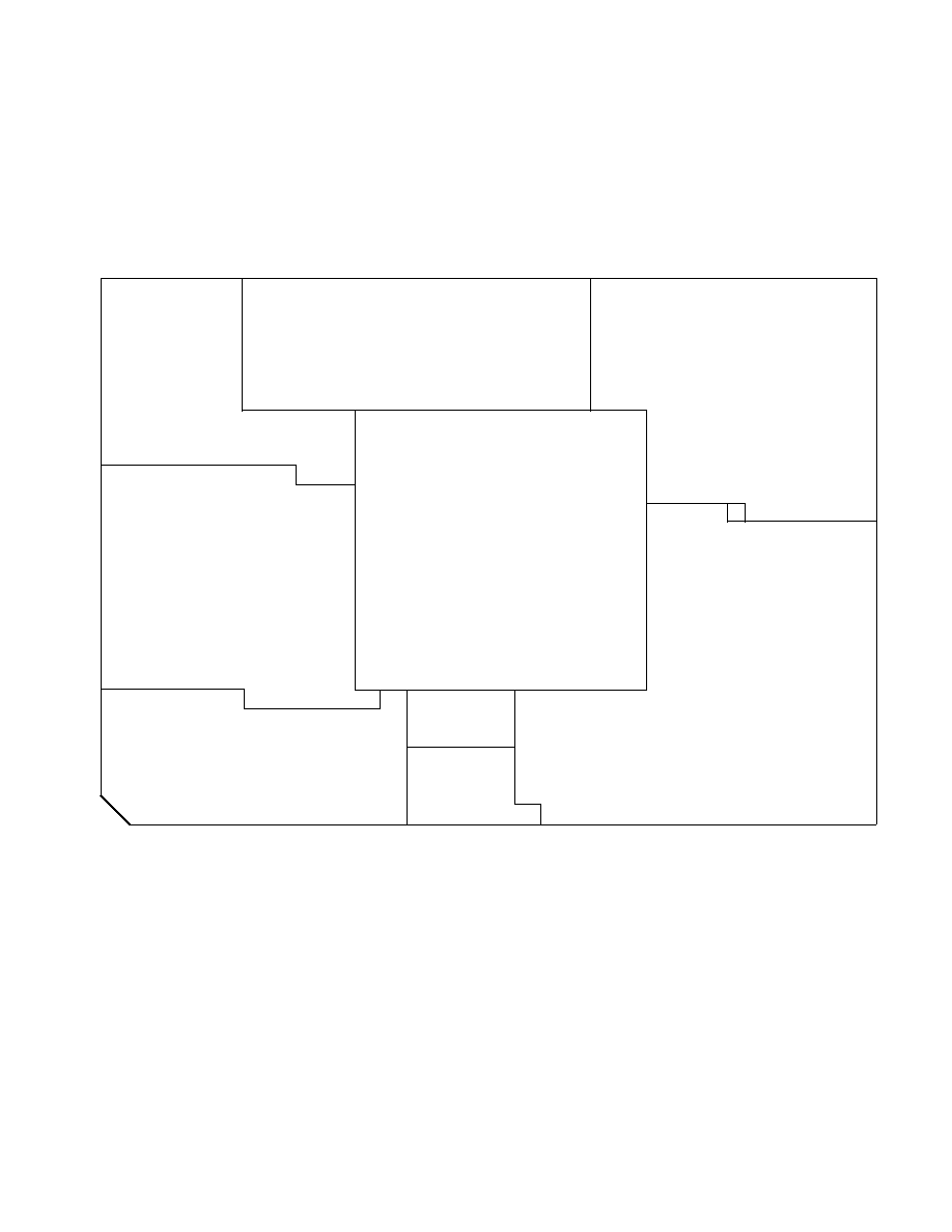
Block Diagram
The C-5e
TM
NP, has an architecture specifically designed for networking applications. The
following sections describe each component of the C-5e NP.
The main components of the C-5e NP are:
�
Channel Processors
�
Executive Processor
�
Fabric Processor
�
Buffer Management Unit
�
Table Lookup Unit
�
Queue Management Unit
The C-5e NP conforms with both SONET and SDH. Therefore, OC-3(STS-3/STM-1), OC-12
(STS-12/STM-4, and OC48 (STS-48/STM-16).
Figure 1
shows a block diagram of the C-5e NP, including its potential external interfaces.
For more information about the architecture of the C-5e NP, see the C-5e/C-3e Network
Processor Architecture Guide (part number C5EC3EARCH-RM/D).

Block Diagram
21
MOTOROLA GENERAL BUSINESS INFORMATION
C5ENPA1-DS/D REV 03
Figure 1 C-5e Network Processor Block Diagram
PHY
PHY
PHY
PHY
PHY
PHY
PHY
PHY
Buses (68Gbps Bandwidth)
Cluster
Cluster
CP-1
CP-0
CP-2
CP-3
CP-12 CP-13 CP-14 CP-15
External
Host CPU
(optional)
OC-3
PHY Interface Examples:
OC-12
Gigabit Ethernet - Aggregated
10/100 Ethernet
External
PROM
(optional)
Control
Logic
(optional)
Fabric
Processor Boundary
Buffer
Mgmt
Unit
Channel
Processors
SDRAM
C-5e
NP
SRAM
SRAM
Table
Lookup
Unit
Fabric
Processor
Executive Processor
Queue
Mgmt
Unit
PCI
Serial
PROM
1xOC-48c or 48x STS-1 with M-5 Companion Device
Q-5
(optional)

22
CHAPTER 1: FUNCTIONAL DESCRIPTION
C5ENPA1-DS/D REV 03
MOTOROLA GENERAL BUSINESS INFORMATION
Channel Processors
The C-5e NP contains sixteen programmable Channel Processors (CPs) that receive,
process, and transmit network data. The number of CPs per port is configurable,
depending on the line interface. Typically one CP is assigned to each port for medium
bandwidth applications (Fast Ethernet to OC-3). Multiple CPs can be assigned to a port in
a configuration called channel aggregation in high bandwidth applications (greater than
OC-3). Multiple logical ports can be assigned to a single CP, with the addition of an
external multiplexor, for low bandwidth applications, such as DS1 to DS3.
The C-5e NP's architecture supports a variety of industry-standard serial and parallel
protocols and individual port data rates including:
�
10/100Mb Ethernet (RMII)
�
1Gb Ethernet (GMII and TBI)
�
OC-3c
�
OC-12
�
OC-48c (using various configurations with M-5 Channel Adapter)
�
OC-48 (using various configurations with M-5 Channel Adapter)
�
100Mbit FibreChannel
�
DS1/DS3, supported through the use of external framers/multiplexors
The C-5e NP's programmability can also support a variety of special interfaces, such as
various xDSL encapsulations and proprietary protocols.
Key components of each CP are a RISC Core (CPRC) that orchestrates cell/packet
processing and a set of microprogrammable, special-purpose processors, called Serial
Data Processors (SDPs), that provide features such as Ethernet MAC and SONET/SDH
framing, multichannel HDLC, and ATM cell delineation. This means you usually only need
to include PHYs to complete the system.

Executive Processor
23
MOTOROLA GENERAL BUSINESS INFORMATION
C5ENPA1-DS/D REV 03
Executive Processor
The Executive Processor (XP) serves as a centralized computing resource for the C-5e NP
and manages the system interfaces.
The XP performs conventional supervisory tasks in the C-5e NP, including:
�
Reset and initialization of the C-5e NP
�
Program loading and control of CPs
�
Centralized exception handling
�
Management of a host interface through the PCI
�
Management of system interfaces (PCI, Serial Bus, PROM)
System Interfaces
The system interfaces to the XP are:
�
PCI -- Provides an industry standard 32bit 33/66MHz PCI channel used for chip-level
shared resources. The PCI has both initiator and target capabilities. The PCI interface is
typically connected to a host processor.
�
Serial Bus Interface -- Provides a general purpose bi-directional, two-wire serial bus
and I/O port that allows the C-5e NP to control external logic with either of two
standard protocols:
� The MDIO (high-speed) protocol: uses a 16bit data format with 10bits of
addressing and supports transfers up to 25MHz.
� The low-speed protocol: uses an 8bit data format followed by an acknowledge bit
and supports transfers up to 400kbps.
Software is used to select which protocol to use, by setting the appropriate bits in the
Serial Bus Configuration Register. When a serial bus transfer is active, an external pin is
driven by the C-5e NP to indicate which protocol is being used (SPLD=0 indicates
MDIO protocol; SPLD=1 indicates low-speed protocol).
Both SIDA and SICL are bi-directional lines that are connected, via an external pull-up
resistor, to a positive supply voltage. When the bus is free, both lines are HIGH because
of the pull-up resistor. The output stages of the devices connected to the bus must
have either an open-drain or open-collector in order to perform the wired-AND
function required for its arbitration mechanism.

24
CHAPTER 1: FUNCTIONAL DESCRIPTION
C5ENPA1-DS/D REV 03
MOTOROLA GENERAL BUSINESS INFORMATION
�
PROM Interface -- Allows the XP to boot from nonvolatile, flash memory. The PROM
interface is a low-speed, serial I/O port that runs at
1
/
2
to
1
/
16
the core clock rate. The
maximum PROM size addressable is 4MBytes, and must use a "by 16" part. External
board logic is required to perform serial-to-parallel conversion for PROM address
outputs and parallel-to-serial conversion for PROM data inputs.
Fabric Processor
The Fabric Processor (FP) acts as a high-speed network interface port with advanced
functionality. It allows the C-5e NP to interface to an application-specific switching
solution internal to your design. The FP port supports the bidirectional transfer of
segments from the C-5e NP to a hardware interface that provides connectivity to other
network processors or other similar line processing hardware. There are numerous
parameters that can be configured within the FP to allow the interface to be adapted to
different fabric protocols. The FP can be configured to conform to seven (7) different
fabric interfaces that include: CSIX-L1, UTOPIA-1, -2, -3, PRIZMA, Power X(CSIX-L0), and
UTOPIA3 like to M-5.
The FP can be configured to run at any frequency up to 125MHz, with the receive and
transmit data buses up to 32 bits wide. This allows a wide range of supported bandwidths
to and from the switching fabric, all the way up to 4000 Mbps full duplex bandwidth.
Buffer Management Unit
The Buffer Management Unit (BMU) interfaces the C-5e NP to external pipeline
architecture, Single Data Rate Synchronous DRAM. The external memory is partitioned
and used as buffers for receiving and transmitting data between CPs, the FP, and the XP. It
is also used as second level storage in the XP memory hierarchy.
The interface to an array of SDRAM chips is 139bits wide, composed of 128 data bits, two
internal control bits, and nine SECDED (single error correction-double error detection) ECC
(error correction code) bits. The interface is compliant with the PC100 standard and
operates at up to 133MHz with 3.3V LVTTL-compatible inputs and outputs. The refresh
period, Trcd, Tcas, Trp, Tmrd, and Trc are configurable via boot time configuration (see the
C-5e/C-3e Network Processor Architecture Guide (part number C5EC3EARCH-RM/D) for more
details).
The C-5e NP non-configurable interface transfers four beats of data for each read and
write using a sequential burst type. In addition, the C-5e NP uses an auto-refresh mode for
the RAM's.

Table Lookup Unit
25
MOTOROLA GENERAL BUSINESS INFORMATION
C5ENPA1-DS/D REV 03
Some of these parameters are programmed into the SDRAMs' mode register and can be
applied only once per power cycle. The ECC functionality can be enabled or disabled via
configuration register writes.
If needed, the interface can narrowed to 128bits by disabling ECC and providing board
pull-ups for the two control bits and nine ECC bits. This is useful if DIMMs are used in the
board design. If individual SDRAM parts are used, x16 and x32 are supported. The BMU
supports SDRAM devices that use 12 address lines. Internal address calculation paths limit
the maximum memory size to 128MBytes. Only one physical bank of SDRAM is supported.
Table Lookup Unit
The Table Lookup Unit (TLU) performs table lookups in external SRAM. It can also be used
for statistics accumulation and retrieval and as general data storage. The TLU
simultaneously supports multiple application-defined tables and multiple search
strategies, such as those needed for routing, circuit switching, and QoS lookup tasks.
The C-5e NP uses external 64bit wide ZBT Pipelined Bursting Static RAM (SRAM) modules
(at frequencies up to 133MHz) for storage of its tables. These modules allow
implementation of tables with 2
25
x 64bit entries using 8Mbit SRAM technology. The
maximum amount of memory supported by the TLU is 128MBytes in four banks, when
SRAM technology supports 4M x 18pins parts.
Table 5 TLU SRAM Configurations
SRAM TECHNOLOGY
MIN TABLE SIZE
(ONE BANK)
MAXIMUM TABLE SIZE
(FOUR BANKS)
1Mbit (32k x 32pins)
256kBytes
1MBytes
2Mbit (64k x 32pins)
512kBytes
2MBytes
4Mbit (256k x 18pins)
2MBytes
8MBytes
8Mbit (512k x 18pins)
4MBytes
16MBytes
16Mbit (1M x 18pins)
8MBytes
32MBytes
32Mbit (2M x 18pins)
16MBytes
64MBytes
64Mbit (4M x 18pins)
32MBytes
128MBytes

26
CHAPTER 1: FUNCTIONAL DESCRIPTION
C5ENPA1-DS/D REV 03
MOTOROLA GENERAL BUSINESS INFORMATION
Queue Management Unit
The Queue Management Unit (QMU) autonomously manages a number of
application-defined descriptor queues. It handles inter-CP and inter-C-5e NP descriptor
flows by providing switching and buffering. It also performs descriptor replication for
multicast applications. A number of up to 128 queues can be assigned to each CPRC for
QoS-based services.
The QMU provides a queuing engine internal to the chip and uses external SRAM to store
the descriptors. Scheduling is done by the CPs. The QMU supports up to 512 queues and
16, 384 descriptor buffers. A descriptor buffer holds an application-defined "descriptor",
which is a structure that defines the payload buffer handle and other attributes of the
forwarded cell or packet.
The QMU's external SRAM interface uses ZBT synchronous SRAMs organized in a single
bank of up to 128k, 32bit words. This interface runs at up to 175MHz frequency.
The C-5e provides two modes for managing queues. They consist of:
�
Internal Mode (using the internal QMU only)
�
External Mode (using the internal QMU and the external Q-5 Traffic Management
Coprocessor)
See the C-5e/C-3e Network Processor Architecture Guide (part number C5EC3EARCH-RM/D),
as well as, the Q-5/Q-3 Traffic Management Coprocessor Architecture Guide (part number
Q5Q3ARCH-RM/D)
for more details.

MOTOROLA GENERAL BUSINESS INFORMATION
C5ENPA1-DS/D REV 03
C5ENPA1-DS/D
Rev 03
Chapter 2
SIGNAL DESCRIPTIONS
Signal Summary
There are ten (10) functional groupings of signals in the C-5e Network Processor:
�
Clock -- 11 pins
�
Channel Processors (CP0 - CP15) -- 16x7 = 112 pins
�
Executive Processor (XP) -- 57 pins
� PCI Interface -- 50 pins
� PROM Interface -- 4 pins
� Serial Bus Interface -- 2 pins
� General System Interface -- 1 pin
�
Fabric Processor (FP) -- 80 pins
�
Buffer Management Unit (BMU) -- 160 pins
�
Table Lookup Unit (TLU) -- 99 pins
�
Queue Management Unit (QMU) -- 59 pins
�
Power -- 245 pins
�
Test -- 14 pins
�
No connection (NC) -- 3 pins
Two (2) of the sections (CPs and FP) are configurable, depending on the type of device
being implemented.

28
CHAPTER 2: SIGNAL DESCRIPTIONS
C5ENPA1-DS/D REV 03
MOTOROLA GENERAL BUSINESS INFORMATION
Pinout Diagram
The C-5e NP contains 840 pins. These pin numbers are referenced throughout the
remaining chapter.
Figure 2
shows the pin locations from the top view. In contrast,
Figure 3
shows the pin locations from the bottom view.
Figure 2 Pin Locations (Top View)
29
28
27
26
25
23
22
21
20
19
18
17
16
15
14
13
12
11
10
9
8
7
6
5
4
3
2
1
AJ
CP0_0
CP1_0
CP1_5 CP2_4
CP3_4
CP5_2 CP6_1
CP7_1
CP8_1
CP8_6
FOUT0 FOUT6 FOUT12 FOUT19 FOUT24
FOUT31 FTXCTL5
FIN3
FIN10
FIN15
FIN22
FIN29
FRXCTL3
PAD0
PAD1
PAD2
PAD3
PAD4
AJ
AH
CP0_1
VDD33
CP1_6 CP2_5
CP3_5
CP5_3 CP6_2
CP7_2
VDD33
CP9_0
FOUT1 FOUT7 FOUT13
GND
FOUT25
FTXCTL0 FTXCTL6
FIN4
VDDF
FIN16
FIN23
FIN30
GND
PAD5
PAD6
PAD7
VDD33
PAD8
AH
AG
CP0_2
CP1_1
CP2_0 CP2_6
CP3_6
CP5_4 CP6_3
CP7_3
CP8_2
CP9_1
FOUT2
VDDF
FOUT14 FOUT20 FOUT26
VDDF
FTXCLK
FIN5
FIN11
FIN17
FIN24
FIN31
FRXCTL4
PAD9
PAD10
PAD11
PAD12
PAD13
AG
AF
CP0_3
CP1_2
VDD33 CP3_0
CP4_0
GND
CP6_4
CP7_4
CP8_3
CP9_2
GND
FOUT8 FOUT15 FOUT21 FOUT27
FTXCTL1
GND
FIN6
FIN12
FIN18
FIN25
GND
FRXCTL5
PAD14
PAD15
VDD33
PAD16
PAD17
AF
AE
CP0_4
GND
CP2_1 CP3_1
CP4_1
CP5_5 CP6_5
CP7_5
GND
CP9_3
FOUT3 FOUT9 FOUT16
VDDF
FOUT28
FTXCTL2
FIN0
FIN7
GND
FIN19
FIN26
FRXCTL0
VDDF
PAD18
PAD19
PAD20
GND
PAD21
AE
AD
CP0_5
CP1_3
CP2_2 CP3_2
CP4_2
CP5_6 CP6_6
CP7_6
CP8_4
CP9_4
FOUT4 FOUT10 FOUT17 FOUT22 FOUT29
FTXCTL3
FIN1
FIN8
FIN13
FIN20
FIN27
FRXCTL1 FRXCTL6
PAD22
PAD23
PAD24
PAD25
PAD26
AD
AC
CP0_6
CP1_4
CP2_3 CP3_3
CP4_3
CP6_0 CP7_0
CP8_0
CP8_5
CP9_5
FOUT5 FOUT11 FOUT18 FOUT23 FOUT30
FTXCTL4
FIN2
FIN9
FIN14
FIN21
FIN28
FRXCTL2 FRXCLK
PAD27
PAD28
PAD29
PAD30
PAD31
AC
AB
CP9_6
CPA_0 VDD33 CPA_1 CPA_2
GND
CPA_4
CPA_5
VDD33
GND
VDD33
GND
VDDF
GND
VDDF
GND
VDDF
GND
VDD33 PTRDYX
PIRDYX
GND
PCBEX0 PCBEX1
PCBEX2
VDD33 PCBEX3
PPAR
AB
AA
CPA_6
GND
CPB_0 CPB_1 CPB_2
CPB_3 CPB_4
CPB_5
GND
VDD
GND
VDD
GND
VDD
GND
VDD
GND
VDD
GND
PREQX
PRSTX
PCLK
VDD33
PSTOPX PDEVSELX PPERRX
GND
PSERRX
AA
Y
CPB_6 CPC_0 CPC_1 CPC_2 CPC_3
CPC_5 CPC_6
CPD_0
VDD33
GND
VDD
GND
VDD
GND
VDD
GND
VDD
GND
VDDT
PINTA
PIDSEL
PGNTX
SIDA
SICL
SPCK
SPLD
SPDI
SPDO
Y
W
CPD_1 CPD_2 CPD_3 CPD_4 CPD_5
CPE_0 CPE_1
CPE_2
GND
VDD
GND
VDD
GND
VDD
GND
VDD
GND
VDD
GND
PFRAMEX XPUHOT
TA21
TA20
TA19
TA18
TA17
TA16
TA15
W
V
CPE_3
CPE_4
GND
CPE_5 CPE_6
VDD33 CPF_1
CPF_2
VDD33
GND
VDD
GND
VDD
GND
VDD
GND
VDD
GND
VDDT
TA14
TA13
VDDT
TA12
TA11
TA10
GND
TA9
TA8
V
U
CPF_3
VDD33
CPF_4 CPF_5 CPF_6
MD0
MD1
MD2
GND
VDD
GND
VDD
GND
VDD
GND
VDD
GND
VDD
GND
TA7
TA6
TA5
GND
TA4
TA3
TA2
VDDT
TA1
U
T
MD3
MD4
MD5
MD6
MD7
MD9
MD10
MD11
VDD33
GND
VDD
GND
VDD
GND
VDD
GND
VDD
GND
VDDT
TWE3X
TWE2X
TWE1X
TWE0X
TCE3X
TCE2X
TCE1X
TCE0X
TA0
T
R
MD12
MD13
MD14
MD15
MD16
MD18
MD19
MD20
GND
VDD
GND
VDD
GND
VDD
GND
VDD
GND
VDD
GND
TD63
TD62
TD61
TD60
TPAR3
TPAR2
TPAR1
TPAR0
TCLKI
R
P
MD21
MD22
VDD33
MD23
MD24
GND
MD26
MD27
VDD33
GND
VDD
GND
VDD
GND
VDD
GND
VDD
GND
VDDT
TD59
TD58
GND
TD57
TD56
TD55
VDDT
TD54
TD53
P
N
MD28
GND
MD29
MD30
MD31
MD32
MD33
MD34
GND
VDD
GND
VDD
GND
VDD
GND
VDD
GND
VDDT
GND
TD52
TD51
TD50
VDDT
TD49
TD48
TD47
GND
TD46
N
M
MD35
MD36
MD37
MD38
MD39
MD41
MD42
MD43
VDD33
GND
VDD
GND
VDD
GND
VDD
GND
VDD
GND
VDDT
TD45
TD44
TD43
TD42
TD41
TD40
TD39
TD38
TD37
M
L
MD44
MD45
MD46
MD47
MD48
MD50
MD51
MD52
GND
VDD
GND
VDD
GND
VDD
GND
VDD
GND
VDD
GND
TD36
TD35
TD34
TD33
TD32
TD31
TD30
TD29
TD28
L
K
MD53
MD54
GND
MD55
MD56
VDD33 MD58
MD59
VDD33
GND
VDD
GND
VDD
GND
VDD
GND
VDD
GND
VDDT
TD27
TD26
VDDT
TD25
TD24
TD23
GND
TD22
TD21
K
J
MD60
VDD33
MD61
MD62
MD63
MD64
MD65
MD66
GND
VDD
GND
VDD
GND
VDD
GND
VDD
GND
VDDT
GND
TD20
TD19
TD18
GND
TD17
TD16
TD15
VDDT
TD14
J
H
MD67
MD68
MD69
MD70
MD71
MD73
MD74
MD75
VDD33
GND
VDD33
GND
VDD33
GND
VDD33
GND
VDD33
GND
VDDT
TD13
TD12
TD11
TD10
TD9
TD8
TD7
TD6
TD5
H
G
MD76
MD77
MD78
MD79
MD80
MD82
MD83
MD84
MDECC7 MDECC2
MDQM
MA11
MA5
SCLK
CCLK0
CCLK3
CPREF
QA13
TD4
TD3
TD2
TD1
TD0
QD23
QD16
QD11
QD6
QD0
G
F
MD85
MD86
VDD33
MD87
MD88
VDD33 MD90
MD91
MDECC6 MDECC1 MDQML MA10
MA4
SCLKX
CCLK1
CCLK4
CCLK6
QA14
QA9
QA3
QDPH
VDDT
QD30
QD24
QD17
VDDT
QD7
QD1
F
E
MD92
GND
MD93
MD94
MD95
MD96
MD97
MD98
GND
MDECC0
MBA0
MA9
MA3
VDD33
CCLK2
CCLK5
CCLK7
QA15
GND
QA4
QARDY
QBCLKI
GND
QD25
QD18
QD12
GND
QD2
E
D
MD99
MD100 MD101 MD102 MD103
MD105 MD106
MD107 MDECC5
MCASX
GND
MA8
MA2
JSE
JSO0
JSO2
GND
QA16
QA10
QA5
QNQRDY QACLKO
QD31
QD26
QD19
QD13
QD8
QD3
D
C
MD108 MD109
GND
MD110 MD111
VDD33 MD113
MD114 MDECC4
MRASX
MBA1
VDD33
MA1
JTCK JCLKBYP
VDD33
JSO3
QDQPAR QA11
QA6
QA0
VDDT
QWEX
QD27
QD20
GND
QD9
QD4
C
B
MD115 VDD33 MD116 MD117 MD118
MD119 MD120
MD121
VDD33
MWEX
MDCLK
MA7
MA0
GND
JTDI
JHIGHZ
JSO5
NC3
VDDT
QA7
QA1
QACLKI
GND
QD28
QD21
QD14
VDDT
QD5
B
A
MD122 MD123 MD124 MD125 MD126
MD128 MD129 MDECC8 MDECC3
MCSX
NC5
MA6
JSO1
JSO4
JTMS
JTDO
JTRSTX
NC4
QA12
QA8
QA2
QDPL
QBCLKO
QD29
QD22
QD15
QD10
A
29
28
27
26
25
23
22
21
20
19
18
17
16
15
14
13
12
11
10
9
8
7
6
5
4
3
2
1
24
CP4_4
GND
CP4_5
CP4_6
VDD33
CP5_0
CP5_1
CPA_3
VDD33
CPC_4
CPD_6
CPF_0
GND
MD8
MD17
MD25
VDD33
MD40
MD49
MD57
GND
MD72
MD81
MD89
GND
MD104
MD112
GND
MD127
24
Pinout Diagram
29
MOTOROLA GENERAL BUSINESS INFORMATION
C5ENPA1-DS/D REV 03
Figure 3 Pin Locations (Bottom View)
29
28
27
26
25
23
22
21
20
19
18
17
16
15
14
13
12
11
10
9
8
7
6
5
4
3
2
1
AJ
CP0_0
CP1_0
CP1_5
CP2_4
CP3_4
CP5_2
CP6_1
CP7_1
CP8_1
CP8_6
FOUT0
FOUT6
FOUT12
FOUT19
FOUT24
FOUT31
FTXCTL5
FIN3
FIN10
FIN15
FIN22
FIN29
FRXCTL3
PAD0
PAD1
PAD2
PAD3
PAD4
AJ
AH
CP0_1
VDD33
CP1_6
CP2_5
CP3_5
CP5_3
CP6_2
CP7_2
VDD33
CP9_0
FOUT1
FOUT7
FOUT13
GND
FOUT25
FTXCTL0
FTXCTL6
FIN4
VDDF
FIN16
FIN23
FIN30
GND
PAD5
PAD6
PAD7
VDD33
PAD8
AH
AG
CP0_2
CP1_1
CP2_0
CP2_6
CP3_6
CP5_4
CP6_3
CP7_3
CP8_2
CP9_1
FOUT2
VDDF
FOUT14
FOUT20
FOUT26
VDDF
FTXCLK
FIN5
FIN11
FIN17
FIN24
FIN31
FRXCTL4
PAD9
PAD10
PAD11
PAD12
PAD13
AG
AF
CP0_3
CP1_2
VDD33
CP3_0
CP4_0
GND
CP6_4
CP7_4
CP8_3
CP9_2
GND
FOUT8
FOUT15
FOUT21
FOUT27
FTXCTL1
GND
FIN6
FIN12
FIN18
FIN25
GND
FRXCTL5
PAD14
PAD15
VDD33
PAD16
PAD17
AF
AE
CP0_4
GND
CP2_1
CP3_1
CP4_1
CP5_5
CP6_5
CP7_5
GND
CP9_3
FOUT3
FOUT9
FOUT16
VDDF
FOUT28
FTXCTL2
FIN0
FIN7
GND
FIN19
FIN26
FRXCTL0
VDDF
PAD18
PAD19
PAD20
GND
PAD21
AE
AD
CP0_5
CP1_3
CP2_2
CP3_2
CP4_2
CP5_6
CP6_6
CP7_6
CP8_4
CP9_4
FOUT4
FOUT10
FOUT17
FOUT22
FOUT29
FTXCTL3
FIN1
FIN8
FIN13
FIN20
FIN27
FRXCTL1
FRXCTL6
PAD22
PAD23
PAD24
PAD25
PAD26
AD
AC
CP0_6
CP1_4
CP2_3
CP3_3
CP4_3
CP6_0
CP7_0
CP8_0
CP8_5
CP9_5
FOUT5
FOUT11
FOUT18
FOUT23
FOUT30
FTXCTL4
FIN2
FIN9
FIN14
FIN21
FIN28
FRXCTL2
FRXCLK
PAD27
PAD28
PAD29
PAD30
PAD31
AC
AB
CP9_6
CPA_0
VDD33
CPA_1
CPA_2
GND
CPA_4
CPA_5
VDD33
GND
VDD33
GND
VDDF
GND
VDDF
GND
VDDF
GND
VDD33
PTRDYX
PIRDYX
GND
PCBEX0
PCBEX1
PCBEX2
VDD33
PCBEX3
PPAR
AB
AA
CPA_6
GND
CPB_0
CPB_1
CPB_2
CPB_3
CPB_4
CPB_5
GND
VDD
GND
VDD
GND
VDD
GND
VDD
GND
VDD
GND
PREQX
PRSTX
PCLK
VDD33
PSTOPX
PDEVSELX
PPERRX
GND
PSERRX
AA
Y
CPB_6
CPC_0
CPC_1
CPC_2
CPC_3
CPC_5
CPC_6
CPD_0
VDD33
GND
VDD
GND
VDD
GND
VDD
GND
VDD
GND
VDDT
PINTA
PIDSEL
PGNTX
SIDA
SICL
SPCK
SPLD
SPDI
SPDO
Y
W
CPD_1
CPD_2
CPD_3
CPD_4
CPD_5
CPE_0
CPE_1
CPE_2
GND
VDD
GND
VDD
GND
VDD
GND
VDD
GND
VDD
GND
PFRAMEX
XPUHOT
TA21
TA20
TA19
TA18
TA17
TA16
TA15
W
V
CPE_3
CPE_4
GND
CPE_5
CPE_6
VDD33
CPF_1
CPF_2
VDD33
GND
VDD
GND
VDD
GND
VDD
GND
VDD
GND
VDDT
TA14
TA13
VDDT
TA12
TA11
TA10
GND
TA9
TA8
V
U
CPF_3
VDD33
CPF_4
CPF_5
CPF_6
MD0
MD1
MD2
GND
VDD
GND
VDD
GND
VDD
GND
VDD
GND
VDD
GND
TA7
TA6
TA5
GND
TA4
TA3
TA2
VDDT
TA1
U
T
MD3
MD4
MD5
MD6
MD7
MD9
MD10
MD11
VDD33
GND
VDD
GND
VDD
GND
VDD
GND
VDD
GND
VDDT
TWE3X
TWE2X
TWE1X
TWE0X
TCE3X
TCE2X
TCE1X
TCE0X
TA0
T
R
MD12
MD13
MD14
MD15
MD16
MD18
MD19
MD20
GND
VDD
GND
VDD
GND
VDD
GND
VDD
GND
VDD
GND
TD63
TD62
TD61
TD60
TPAR3
TPAR2
TPAR1
TPAR0
TCLKI
R
P
MD21
MD22
VDD33
MD23
MD24
GND
MD26
MD27
VDD33
GND
VDD
GND
VDD
GND
VDD
GND
VDD
GND
VDDT
TD59
TD58
GND
TD57
TD56
TD55
VDDT
TD54
TD53
P
N
MD28
GND
MD29
MD30
MD31
MD32
MD33
MD34
GND
VDD
GND
VDD
GND
VDD
GND
VDD
GND
VDDT
GND
TD52
TD51
TD50
VDDT
TD49
TD48
TD47
GND
TD46
N
M
MD35
MD36
MD37
MD38
MD39
MD41
MD42
MD43
VDD33
GND
VDD
GND
VDD
GND
VDD
GND
VDD
GND
VDDT
TD45
TD44
TD43
TD42
TD41
TD40
TD39
TD38
TD37
M
L
MD44
MD45
MD46
MD47
MD48
MD50
MD51
MD52
GND
VDD
GND
VDD
GND
VDD
GND
VDD
GND
VDD
GND
TD36
TD35
TD34
TD33
TD32
TD31
TD30
TD29
TD28
L
K
MD53
MD54
GND
MD55
MD56
VDD33
MD58
MD59
VDD33
GND
VDD
GND
VDD
GND
VDD
GND
VDD
GND
VDDT
TD27
TD26
VDDT
TD25
TD24
TD23
GND
TD22
TD21
K
J
MD60
VDD33
MD61
MD62
MD63
MD64
MD65
MD66
GND
VDD
GND
VDD
GND
VDD
GND
VDD
GND
VDDT
GND
TD20
TD19
TD18
GND
TD17
TD16
TD15
VDDT
TD14
J
H
MD67
MD68
MD69
MD70
MD71
MD73
MD74
MD75
VDD33
GND
VDD33
GND
VDD33
GND
VDD33
GND
VDD33
GND
VDDT
TD13
TD12
TD11
TD10
TD9
TD8
TD7
TD6
TD5
H
G
MD76
MD77
MD78
MD79
MD80
MD82
MD83
MD84
MDECC7
MDECC2
MDQM
MA11
MA5
SCLK
CCLK0
CCLK3
CPREF
QA13
TD4
TD3
TD2
TD1
TD0
QD23
QD16
QD11
QD6
QD0
G
F
MD85
MD86
VDD33
MD87
MD88
VDD33
MD90
MD91
MDECC6
MDECC1
MDQML
MA10
MA4
SCLKX
CCLK1
CCLK4
CCLK6
QA14
QA9
QA3
QDPH
VDDT
QD30
QD24
QD17
VDDT
QD7
QD1
F
E
MD92
GND
MD93
MD94
MD95
MD96
MD97
MD98
GND
MDECC0
MBA0
MA9
MA3
VDD33
CCLK2
CCLK5
CCLK7
QA15
GND
QA4
QARDY
QBCLKI
GND
QD25
QD18
QD12
GND
QD2
E
D
MD99
MD100
MD101
MD102
MD103
MD105
MD106
MD107
MDECC5
MCASX
GND
MA8
MA2
JSE
JSO0
JSO2
GND
QA16
QA10
QA5
QNQRDY
QACLKO
QD31
QD26
QD19
QD13
QD8
QD3
D
C
MD108
MD109
GND
MD110
MD111
VDD33
MD113
MD114
MDECC4
MRASX
MBA1
VDD33
MA1
JTCK
JCLKBYP
VDD33
JSO3
QDQPAR
QA11
QA6
QA0
VDDT
QWEX
QD27
QD20
GND
QD9
QD4
C
B
MD115
VDD33
MD116
MD117
MD118
MD119
MD120
MD121
VDD33
MWEX
MDCLK
MA7
MA0
GND
JTDI
JHIGHZ
JSO5
NC3
VDDT
QA7
QA1
QACLKI
GND
QD28
QD21
QD14
VDDT
QD5
B
A
MD122
MD123
MD124
MD125
MD126
MD128
MD129
MDECC8
MDECC3
MCSX
NC5
MA6
JSO1
JSO4
JTMS
JTDO
JTRSTX
NC4
QA12
QA8
QA2
QDPL
QBCLKO
QD29
QD22
QD15
QD10
A
29
28
27
26
25
23
22
21
20
19
18
17
16
15
14
13
12
11
10
9
8
7
6
5
4
3
2
1
24
CP4_4
GND
CP4_5
CP4_6
VDD33
CP5_0
CP5_1
CPA_3
VDD33
CPC_4
CPD_6
CPF_0
GND
MD8
MD17
MD25
VDD33
MD40
MD49
MD57
GND
MD72
MD81
MD89
GND
MD104
MD112
GND
MD127
24

30
CHAPTER 2: SIGNAL DESCRIPTIONS
C5ENPA1-DS/D REV 03
MOTOROLA GENERAL BUSINESS INFORMATION
Pin Descriptions Grouped
by Function
The C-5e NP pins are categorized in groups, reflecting interfaces to the chip:
�
Clock Signals
�
CP Interface Signals
�
Executive Processor System Interface Signals
�
Fabric Processor Interface Signals
�
BMU SDRAM Interface Signals
�
TLU SRAM Interface Signals
�
QMU SRAM (Internal Mode) Interface Signals
�
QMU to Q-5 TMC (External Mode) Interface Signals
�
Power Supply Signals
�
Test Signals
�
No Connection Pins
Pins conform to Joint Electronic Devices Engineering Council (JEDEC) standards.
LVTTL and LVPECL
Specifications
C-5e NP pins are the following types:
�
Low Voltage TTL-Compatible (LVTTL). The C-5e NP's LVTTL pins conform to the JEDEC
JESD8-B specification.
�
Low Voltage Positive Emitter Coupled Logic (LVPECL).
All of the signals in the following tables in this chapter denote whether the individual
signal is an Input (I), Output (O), both Input and Output (I/O), or power (P). In addition, a
PU, PD, and nc are used. The PU indicates that an internal resistor will pullup the pad if
left unconnected. PD indicates an internal pulldown resistor. NC means the pad is to be
left unconnected.

Pin Descriptions Grouped by Function
31
MOTOROLA GENERAL BUSINESS INFORMATION
C5ENPA1-DS/D REV 03
Clock Signals
Table 6
describes the C-5e NP clock signals.
Table 6 Clock and Reference Signals
SIGNAL NAME
PIN #
TOTAL
TYPE
I/O
SIGNAL DESCRIPTION
SCLK*
SCLKX*
*
SCLK and SCLKX must not be AC-coupled.
G15
F15
1
1
LVPECL
LVPECL
I
I
Core Clock Rate (Differential)
CCLK0
G14
1
LVTTL
I
PD
1_544MHZ_CLK (T1)
The frequencies specified for CCLK0 - CCLK7 allow full flexibility for the C-5e NP. It is also possible to use one
or more CCLKn inputs for other frequencies. Contact your Motorola representative for more information.
CCLK1
F14
1
LVTTL
I
PD
2_048MHZ_CLK (E1)
CCLK2
E14
1
LVTTL
I
PD
34_368MHZ_CLK (E3)
CCLK3
G13
1
LVTTL
I
PD
44_736MHZ_CLK (T3)
CCLK4
F13
1
LVTTL
I
PD
50MHZ_CLK (100Mbit Ethernet)
CCLK5
E13
1
LVTTL
I
PD
106_25MHZ_CLK (Fibre Channel)
CCLK6
F12
1
LVTTL
I
PD
125MHZ_CLK (Gigabit Ethernet)
CCLK7
E12
1
LVTTL
I
PD
155_52MHZ_CLK (OC-3)
CPREF
If any of the CPs are configured for LVPECL operation (OC3) using the pin mode registers, then CPREF must
be wired to an external reference, as specified in
Table 38
on page 75. If none of the CPs are configured for
LVPECL operation, then the CPREF pin can be left unconnected.
G12
1
LVPECL
I
PD
Reference
TOTAL
11

32
CHAPTER 2: SIGNAL DESCRIPTIONS
C5ENPA1-DS/D REV 03
MOTOROLA GENERAL BUSINESS INFORMATION
CP Interface Signals
The C-5e NP's 16 CPs support various network physical interfaces, providing a serial
interface to the PHY layer. Interfaces are configured via bits in the C-5e NP register set.
Many interfaces are possible by programming the configuration registers. CPs can be
used individually or in a cluster (four CPs) to implement the various interfaces.
Table 7
provides a quick reference of all the CP pins organized by clusters. There are seven
physical I/O pins associated with each CP. All pins are capable of receiving data, with some
configurable to be input clocks, output clocks, or data drivers. In addition, pairs of pins can
be configured as differential pairs for LVPECL compatibility.
In the case of RMII, OC-3, DS1, and DS3, the drivers and receivers at the pin are locally
configured to match the relevant PHY or Framer chip. OC-12 uses the aggregation of four
CPs (one cluster), while GMII and Ten Bit Interface (TBI) can use either eight CPs (four for
receive and four for transmit) or four CPs that share the transmit and receive functions for
non-wire speed applications.
During CP aggregation, all 28 pins associated with a cluster are routed to all of the Serial
Data Processors (SDPs) in that cluster. This allows round-robin usage of portions of the
SDPs, with each getting access to the necessary I/O pins.
The signals for the following CP physical interfaces are included in this section:
�
DS1/T1 Framer Interface Configuration
�
10/100 Ethernet (RMII) Configuration
�
Gigabit Ethernet (GMII) Configuration
�
Gigabit Ethernet and Fibre Channel TBI Configuration
�
SONET OC-3 Transceiver Interface Configuration
�
SONET OC-12 Transceiver Interface Configuration

Pin Descriptions Grouped by Function
33
MOTOROLA GENERAL BUSINESS INFORMATION
C5ENPA1-DS/D REV 03
Table 7 CP Physical Interface Signals and Pins (Grouped by Clusters)
CP CLUSTER 1
CP CLUSTER 2
CP CLUSTER 3
CP CLUSTER 4
SIGNAL
PIN #
SIGNAL
PIN #
SIGNAL
PIN #
SIGNAL
PIN #
CP0_0
AJ29
CP4_0
AF25
CP8_0
AC21
CPC_0
Y28
CP0_1
AH29
CP4_1
AE25
CP8_1
AJ20
CPC_1
Y27
CP0_2
AG29
CP4_2
AD25
CP8_2
AG20
CPC_2
Y26
CP0_3
AF29
CP4_3
AC25
CP8_3
AF20
CPC_3
Y25
CP0_4
AE29
CP4_4
AJ24
CP8_4
AD20
CPC_4
Y24
CP0_5
AD29
CP4_5
AG24
CP8_5
AC20
CPC_5
Y23
CP0_6
AC29
CP4_6
AF24
CP8_6
AJ19
CPC_6
Y22
CP1_0
AJ28
CP5_0
AD24
CP9_0
AH19
CPD_0
Y21
CP1_1
AG28
CP5_1
AC24
CP9_1
AG19
CPD_1
W29
CP1_2
AF28
CP5_2
AJ23
CP9_2
AF19
CPD_2
W28
CP1_3
AD28
CP5_3
AH23
CP9_3
AE19
CPD_3
W27
CP1_4
AC28
CP5_4
AG23
CP9_4
AD19
CPD_4
W26
CP1_5
AJ27
CP5_5
AE23
CP9_5
AC19
CPD_5
W25
CP1_6
AH27
CP5_6
AD23
CP9_6
AB29
CPD_6
W24
CP2_0
AG27
CP6_0
AC23
CPA_0
AB28
CPE_0
W23
CP2_1
AE27
CP6_1
AJ22
CPA_1
AB26
CPE_1
W22
CP2_2
AD27
CP6_2
AH22
CPA_2
AB25
CPE_2
W21
CP2_3
AC27
CP6_3
AG22
CPA_3
AB24
CPE_3
V29
CP2_4
AJ26
CP6_4
AF22
CPA_4
AB22
CPE_4
V28
CP2_5
AH26
CP6_5
AE22
CPA_5
AB21
CPE_5
V26
CP2_6
AG26
CP6_6
AD22
CPA_6
AA29
CPE_6
V25
CP3_0
AF26
CP7_0
AC22
CPB_0
AA27
CPF_0
V24
CP3_1
AE26
CP7_1
AJ21
CPB_1
AA26
CPF_1
V22
CP3_2
AD26
CP7_2
AH21
CPB_2
AA25
CPF_2
V21
CP3_3
AC26
CP7_3
AG21
CPB_3
AA23
CPF_3
U29
CP3_4
AJ25
CP7_4
AF21
CPB_4
AA22
CPF_4
U27
CP3_5
AH25
CP7_5
AE21
CPB_5
AA21
CPF_5
U26
CP3_6
AG25
CP7_6
AD21
CPB_6
Y29
CPF_6
U25

34
CHAPTER 2: SIGNAL DESCRIPTIONS
C5ENPA1-DS/D REV 03
MOTOROLA GENERAL BUSINESS INFORMATION
DS1/T1 Framer Interface Configuration
Table 8
describes the serial framer interface signals. For each CP (0-15), you can
implement one serial Framer interface.
10/100 Ethernet (RMII) Configuration
Table 9
describes the 10/100BASE-T Ethernet Reduced Media Independent Interface
(RMII) signals. For each CP (0-15), you can implement one 10/100 Ethernet interface.
Table 8 DS1/T1 Framer Interface Signals
SIGNAL NAME*
PIN #
TOTAL
TYPE
I/O
LABEL
SIGNAL DESCRIPTION
CPn_0
Table 7
1
LVTTL
O
PD
TCLK
Transmit Clock (1.544MHz)
CPn_1
Table 7
1
LVTTL
I
PU
RCLK
Receive Clock (1.544MHz)
CPn_2
Table 7
1
LVTTL
O
PD
TData
Transmit Data
CPn_3
Table 7
1
LVTTL
O
PU
TFrame
Transmit Frame Synchronization
CPn_4
Table 7
1
LVTTL
I
PD
RData
Receive Data
CPn_5
Table 7
1
LVTTL
I
PU
RFrame
Receive Frame Synchronization
CPn_6
Table 7
1
nc
nc
PU
nc
nc
TOTAL PINS
7
*
n can be from 0 to 15. See
Table 7
.
Reference
Table 7
for pin numbers for the actual cluster(s) you are configuring.
Table 9 10/100 Ethernet Signals
SIGNAL NAME*
PIN #
TOTAL
TYPE
I/O
LABEL
SIGNAL DESCRIPTION
CPn_0
Table 7
1
LVTTL
O
PD
REF_CLK
Transmit and Receive Clock (50MHz)
CPn_1
Table 7
1
LVTTL
I
PU
CRS_DV
Carrier Sense (CRS)/ Receive Data Valid (RX_DV). CRS indicates that
traffic is on the link, and is asserted if the signal is a 1 or an
alternating 1010... RX_DV indicates that a receive frame is in
progress and the data present on the RXD pins is valid. It is
asserted if this signal is a 1 for more than one cycle.
CPn_2
Table 7
1
LVTTL
O
PD
TXD(0)
Transmit Data 0 (first on wire)
CPn_3
Table 7
1
LVTTL
O
PU
TXD(1)
Transmit Data 1 (second on wire)
CPn_4
Table 7
1
LVTTL
I
PD
RXD(0)
Receive Data 0 (first on wire)
CPn_5
Table 7
1
LVTTL
I
PU
RXD(1)
Receive Data 1 (second on wire)
CPn_6
Table 7
1
LVTTL
O
PU
TX_EN
Transmit Enable. When asserted, the data on TXD is encoded and
transmitted on the twisted pair cable.
TOTAL PINS
7
*
n can be from 0 to 15. See
Table 7
.

Pin Descriptions Grouped by Function
35
MOTOROLA GENERAL BUSINESS INFORMATION
C5ENPA1-DS/D REV 03
Gigabit Ethernet (GMII) Configuration
Gigabit Ethernet Media Independent Interface (GMII) is configured in one of two ways:
�
Use one CP cluster when density is more important than wire-speed performance
because you can then implement up to four Gigabit Ethernet ports per C-5e NP.
�
Use two CP clusters for wire-speed performance and additional processing power. You
can implement up to two Gigabit Ethernet ports per C-5e NP.
Table 10
lists the possible CP cluster combinations you can use and
Figure 4
shows receive
and transmit pin configurations by cluster.
Table 11
lists the signals and pinouts for
Gigabit Ethernet (GMII).
Table 10 Transmit and Receive Pin Combinations for Gigabit Ethernet and Fibre Channel
CLUSTER
SINGLE CLUSTER MODE (TBI OR GMII)
TWO CLUSTER MODE (GMII)*
*
The Two Cluster Mode column lists typical configurations. Any cluster can be set up to either receive
or transmit. So you could configure a dual cluster mode where cluster 0 receives and cluster 3
transmits.
0
Port 1 Tx and Rx
Port 1 Tx
1
Port 2 Tx and Rx
Port 1 Rx
2
Port 3 Tx and Rx
Port 2 Tx
3
Port 4 Tx and Rx
Port 2 Rx

36
CHAPTER 2: SIGNAL DESCRIPTIONS
C5ENPA1-DS/D REV 03
MOTOROLA GENERAL BUSINESS INFORMATION
Figure 4 GMII/TBI Transmit and Receive Pin Configurations
Cluster
0
Cluster
1
Cluster
2
Cluster
3
Port 1
Port 2
Port 3
Port 4
}
}
}
}
Tx
Tx
Tx
Tx
Rx
Rx
Rx
Rx
Single Cluster Mode
Pin Configuration
Port 1
Port 2
}
Tx
Tx
Tx
Tx
Rx
Rx
Rx
Rx
Two Cluster Mode
Pin Configuration
nc
nc
nc
nc
}
nc = not connected
Cluster
0
Cluster
1
Cluster
2
Cluster
3
Table 11 Gigabit Ethernet (GMII/MII) Signals One Cluster Example
SIGNAL NAME*
PIN #
TOTAL
TYPE
I/O
LABEL
SIGNAL DESCRIPTION
CPn_0
Table 7
1
LVTTL
O
PD
T_CLK
GMII Transmit Clock (125MHz). This clock is used to synchronize the
transmit data.
CPn_1
Table 7
1
LVTTL
I
PU
TCLKI
MII transmit clock. Transmit data aligned to this clock input from
phy in MII mode. 25 Mhz in 100BaseT, 2.5 in Mhz in 10BaseT
CPn_2
Table 7
1
LVTTL
O
PD
TXD(0)
Transmit Data (byte-wide data, least significant bit)
CPn_3
Table 7
1
LVTTL
O
PU
TXD(1)
Transmit Data
CPn_4
Table 7
1
LVTTL
O
PD
TXD(2)
Transmit Data
CPn_5
Table 7
1
LVTTL
O
PU
TXD(3)
Transmit Data
CPn_6
Table 7
1
LVTTL
O
PU
TX_EN
Transmit Enable. When asserted, the data on TXD is encoded and
transmitted on the twisted pair cable.

Pin Descriptions Grouped by Function
37
MOTOROLA GENERAL BUSINESS INFORMATION
C5ENPA1-DS/D REV 03
CPn+1_0
Table 7
1
nc
nc
PD
nc
nc
CPn+1_1
Table 7
1
LVTTL
I
PU
COL
Collision. Asserted when both RX_DV and TX_EN are valid during
half duplex operation.
CPn+1_2
Table 7
1
LVTTL
O
PD
TXD(4)
Transmit Data
CPn+1_3
Table 7
1
LVTTL
O
PU
TXD(5)
Transmit Data
CPn+1_4
Table 7
1
LVTTL
O
PD
TXD(6)
Transmit Data
CPn+1_5
Table 7
1
LVTTL
O
PU
TXD(7)
Transmit Data (byte-wide receive data, most significant bit)
CPn+1_6
Table 7
1
LVTTL
O
PU
TX_ER
Transmit Error. Asserting TX_ER when TX_EN is a 1 causes
transmission of the designated "bad code" in lieu of the normal
encoded data on the twisted pair data.
CPn+2_0
Table 7
1
nc
nc
PD
nc
nc
CPn+2_1
Table 7
1
LVTTL
I
PU
RCLK
Receive Clock (125MHz)
CPn+2_2
Table 7
1
LVTTL
I
PD
RXD(0)
Receive Data (byte-wide receive data, least significant bit)
CPn+2_3
Table 7
1
LVTTL
I
PU
RXD(1)
Receive Data
CPn+2_4
Table 7
1
LVTTL
I
PD
RXD(2)
Receive Data
CPn+2_5
Table 7
1
LVTTL
I
PU
RXD(3)
Receive Data
CPn+2_6
Table 7
1
LVTTL
I
PU
RX_DV
Receive Data Valid. Indicates that there is a receive frame in progress
and that the data present on the RXD signals is valid.
CPn+3_0
Table 7
1
nc
nc
PD
nc
nc
CPn+3_1
Table 7
1
LVTTL
I
PU
CRS
Carrier Sense. Indicates traffic is on the link. CRS is asserted when a
non-idle condition is detected on the receive data stream. CRS is
deasserted when an end of frame or idle condition is detected.
CPn+3_2
Table 7
1
LVTTL
I
PD
RXD(4)
Receive Data
CPn+3_3
Table 7
1
LVTTL
I
PU
RXD(5)
Receive Data
CPn+3_4
Table 7
1
LVTTL
I
PD
RXD(6)
Receive Data
CPn+3_5
Table 7
1
LVTTL
I
PU
RXD(7)
Receive Data (most significant bit)
CPn+3_6
Table 7
1
LVTTL
I
PU
RX_ER
Receive Error Detected. Indicates that there has been an error
received in the receive frame.
TOTAL PINS
28
*
n can be 0, 4, 8, or 12.
Reference
Table 7
for pin numbers for the actual cluster(s) you are configuring.
Table 11 Gigabit Ethernet (GMII/MII) Signals One Cluster Example (continued)
SIGNAL NAME*
PIN #
TOTAL
TYPE
I/O
LABEL
SIGNAL DESCRIPTION

38
CHAPTER 2: SIGNAL DESCRIPTIONS
C5ENPA1-DS/D REV 03
MOTOROLA GENERAL BUSINESS INFORMATION
Gigabit Ethernet and Fibre Channel TBI Configuration
1000BASE-T Gigabit Ethernet and Fibre Channel TBI is implemented in much the same
way as Gigabit Ethernet (GMII).
Table 10
shows the possible CP pin combinations you can
use and
Figure 4
shows receive and transmit pin configurations by cluster.
Table 12
shows
the signals and pinouts for a single cluster for Gigabit Ethernet and Fibre Channel TBI.
The unused pins for the two cluster configurations should be wired down using a resistor.
Table 12 Gigabit Ethernet and Fibre Channel TBI Signals Example
SIGNAL NAME*
PIN #
TOTAL
TYPE
I/O
LABEL
SIGNAL DESCRIPTION
CPn_0
Table 7
1
LVTTL
O
PD
TCLK
Transmit Clock (125MHz). This clock is used to synchronize the
transmit data.
CPn_1
Table 7
1
nc
nc
PU
nc
nc
CPn_2
Table 7
1
LVTTL
O
PD
TXD(9)
Transmit Data (ten bits wide, last on wire)
CPn_3
Table 7
1
LVTTL
O
PU
TXD(8)
Transmit Data
CPn_4
Table 7
1
LVTTL
O
PD
TXD(7)
Transmit Data
CPn_5
Table 7
1
LVTTL
O
PU
TXD(6)
Transmit Data
CPn_6
Table 7
1
LVTTL
O
PU
TXD(1)
Transmit Data
CPn+1_0
Table 7
1
nc
nc
PD
nc
nc
CPn+1_1
Table 7
1
nc
nc
PU
nc
nc
CPn+1_2
Table 7
1
LVTTL
O
PD
TXD(5)
Transmit Data
CPn+1_3
Table 7
1
LVTTL
O
PU
TXD(4)
Transmit Data
CPn+1_4
Table 7
1
LVTTL
O
PD
TXD(3)
Transmit Data
CPn+1_5
Table 7
1
LVTTL
O
PU
TXD(2)
Transmit Data
CPn+1_6
Table 7
1
LVTTL
O
PU
TXD(0)
Transmit Data (ten bits wide, first on wire)
CPn+2_0
Table 7
1
nc
nc
PD
nc
nc
CPn+2_1
Table 7
1
LVTTL
I
PU
RCLK
Receive Clock (62.5 MHz)
CPn+2_2
Table 7
1
LVTTL
I
PD
RXD(9)
Receive Data (ten bits wide, last on wire)
CPn+2_3
Table 7
1
LVTTL
I
PU
RXD(8)
Receive Data
CPn+2_4
Table 7
1
LVTTL
I
PD
RXD(7)
Receive Data
CPn+2_5
Table 7
1
LVTTL
I
PU
RXD(6)
Receive Data
CPn+2_6
Table 7
1
LVTTL
I
PU
RXD(1)
Receive Data

Pin Descriptions Grouped by Function
39
MOTOROLA GENERAL BUSINESS INFORMATION
C5ENPA1-DS/D REV 03
SONET OC-3 Transceiver Interface Configuration
Table 13
describes the SONET Optical Carrier (OC) 3 transceiver interface signals. For each
CP (0-15), you can implement a single OC-3 interface.
CPn+3_0
Table 7
1
nc
nc
PD
nc
nc
CPn+3_1
Table 7
1
LVTTL
I
PU
RCLKN
Receive Clock Inverted
CPn+3_2
Table 7
1
LVTTL
I
PD
RXD(5)
Receive Data
CPn+3_3
Table 7
1
LVTTL
I
PU
RXD(4)
Receive Data
CPn+3_4
Table 7
1
LVTTL
I
PD
RXD(3)
Receive Data
CPn+3_5
Table 7
1
LVTTL
I
PU
RXD(2)
Receive Data
CPn+3_6
Table 7
1
LVTTL
I
PU
RXD(0)
Receive Data (ten bits wide, first on wire)
TOTAL PINS
28
*
n can be 0, 4, 8, or 12
Reference
Table 7
for pin numbers for the actual cluster(s) you are configuring.
Table 12 Gigabit Ethernet and Fibre Channel TBI Signals Example (continued)
SIGNAL NAME*
PIN #
TOTAL
TYPE
I/O
LABEL
SIGNAL DESCRIPTION
Table 13 OC-3 Signals
SIGNAL NAME*
PIN #
TOTAL
TYPE
I/O
LABEL
SIGNAL DESCRIPTION
CPn_0
Table 7
1
LVPECL
I
PD
RCLK_H
Receive Clock noninverted side of pair (155.52MHz)
CPn_1
Table 7
1
LVPECL
I
PU
RCLK_L
Receive Clock inverted side of pair (155.52MHz)
CPn_2
Table 7
1
LVPECL
O
PD
TXD_H
Transmit Data noninverted side of pair
CPn_3
Table 7
1
LVPECL
I
PU
TXD_L
Transmit Data inverted side of pair
CPn_4
Table 7
1
LVPECL
I
PD
RXD_H
Receive Data noninverted side of pair
CPn_5
Table 7
1
LVPECL
I
PU
RXD_L
Receive Data inverted side of pair
CPn_6
Table 7
1
LVPECL
I
PU
SIGNAL_DET
A light level above a certain threshold is present at the optical
receiver - single ended LVPECL.
TOTAL PINS
7
*
n can be from 0 to 15.
Reference
Table 7
for pin numbers for the actual cluster(s) you are configuring.

40
CHAPTER 2: SIGNAL DESCRIPTIONS
C5ENPA1-DS/D REV 03
MOTOROLA GENERAL BUSINESS INFORMATION
SONET OC-12 Transceiver Interface Configuration
SONET Optical Carrier (OC) 12 is implemented by using one cluster of CPs. At any time, a
CP within a cluster spends half its time performing receive functions, and the other half
performing transmit functions.
Table 14
shows a CP Cluster configured for one OC-12
interface.
Table 14 OC-12 Signals Example
SIGNAL NAME*
PIN #
TOTAL
TYPE
I/O
LABEL
SIGNAL DESCRIPTION
CPn_0
Table 7
1
LVTTL
O
PD
TCLK
Deskewed Transmit Clock (77.76MHz). This clock is used to
synchronize the transmit data.
CPn_1
Table 7
1
LVTTL
I
PU
TCLKI
Transceiver Transmit Clock. This clock sets the frequency of the
transmit data and is typically sourced by the PHY chip.
CPn_2
Table 7
1
LVTTL
O
PD
TXD(0)
Transmit Data (byte-wide data, least significant bit)
CPn_3
Table 7
1
LVTTL
O
PU
TXD(1)
Transmit Data
CPn_4
Table 7
1
LVTTL
O
PD
TXD(2)
Transmit Data
CPn_5
Table 7
1
LVTTL
O
PU
TXD(3)
Transmit Data
CPn_6
Table 7
1
LVTTL
O
PU
00F
Out of Frame
CPn+1_0
Table 7
1
nc
nc
PD
nc
nc
CPn+1_1
Table 7
1
nc
nc
PU
nc
nc
CPn+1_2
Table 7
1
LVTTL
O
PD
TXD(4)
Transmit Data
CPn+1_3
Table 7
1
LVTTL
O
PU
TXD(5)
Transmit Data
CPn+1_4
Table 7
1
LVTTL
O
PD
TXD(6)
Transmit Data
CPn+1_5
Table 7
1
LVTTL
O
PU
TXD(7)
Transmit Data (byte-wide data, most significant bit)
CPn+1_6
Table 7
1
nc
nc
PU
nc
nc
CPn+2_0
Table 7
1
nc
nc
PD
nc
nc
CPn+2_1
Table 7
1
LVTTL
I
PU
RCLK
Receive Clock (77.76MHz)
CPn+2_2
Table 7
1
LVTTL
I
PD
RXD(0)
Receive Data (byte-wide receive data, least significant bit)
CPn+2_3
Table 7
1
LVTTL
I
PU
RXD(1)
Receive Data
CPn+2_4
Table 7
1
LVTTL
I
PD
RXD(2)
Receive Data
CPn+2_5
Table 7
1
LVTTL
I
PU
RXD(3)
Receive Data
CPn+2_6
Table 7
1
LVTTL
I
PU
FP
Frame Synchronization Pulse. This is valid during the third A2 of
the receive SONET frame.
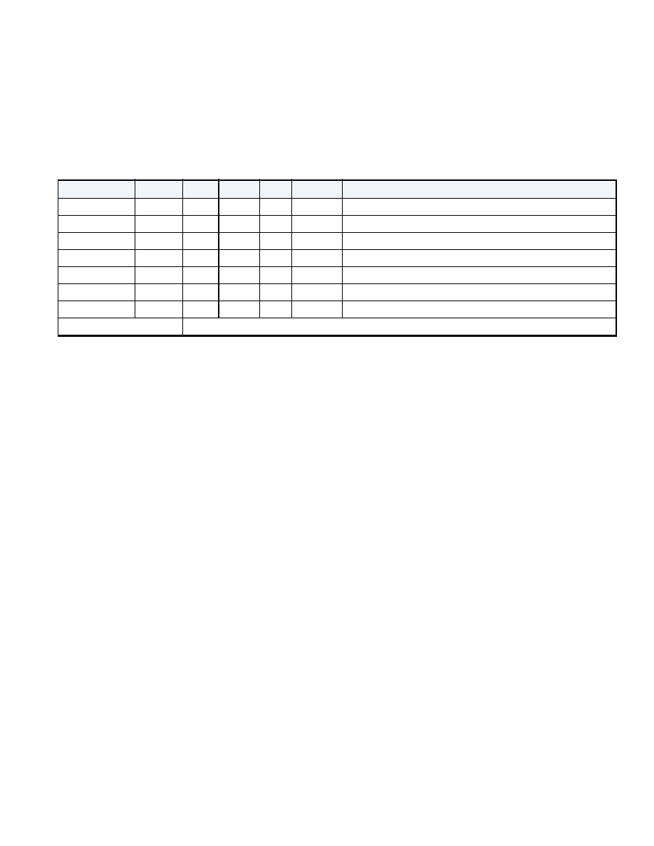
Pin Descriptions Grouped by Function
41
MOTOROLA GENERAL BUSINESS INFORMATION
C5ENPA1-DS/D REV 03
CPn+3_0
Table 7
1
nc
nc
PD
nc
nc
CPn+3_1
Table 7
1
nc
nc
PU
nc
nc
CPn+3_2
Table 7
1
LVTTL
I
PD
RXD(4)
Receive Data
CPn+3_3
Table 7
1
LVTTL
I
PU
RXD(5)
Receive Data
CPn+3_4
Table 7
1
LVTTL
I
PD
RXD(6)
Receive Data
CPn+3_5
Table 7
1
LVTTL
I
PU
RXD(7)
Receive Data (most significant bit)
CPn+3_6
Table 7
1
nc
nc
PU
nc
nc
TOTAL PINS
28
*
n can be 0, 4, 8, or 12
Reference
Table 7
for pin numbers for a different cluster.
Table 14 OC-12 Signals Example (continued)
SIGNAL NAME*
PIN #
TOTAL
TYPE
I/O
LABEL
SIGNAL DESCRIPTION
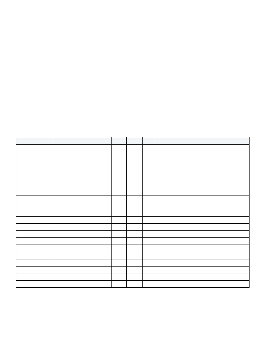
42
CHAPTER 2: SIGNAL DESCRIPTIONS
C5ENPA1-DS/D REV 03
MOTOROLA GENERAL BUSINESS INFORMATION
Executive Processor
System Interface Signals
The XP's system interface manages the supervisory controls for the network interfaces, as
well as the set of pins that provide interfaces to other components in the system that are
not memories or network interfaces. It is also the primary interface used for initializing the
C-5e NP after reset. The XP signals include PCI signals, Serial interface signals, and PROM
interface signals.
PCI Signals
The PCI can be configured to support a 32bit PCI capable of operating at either 33MHz or
66MHz. The PCI is fully compliant with PCI Specification revision 2.1.
Table 15
describes
the PCI signals.
Table 15 PCI Signals
SIGNAL NAME
PIN #
TOTAL
TYPE
I/O
SIGNAL DESCRIPTION
PAD0 - PAD31
AJ5, AJ4, AJ3, AJ2, AJ1, AH5, AH4,
AH3, AH1, AG5, AG4, AG3, AG2,
AG1, AF5, AF4, AF2, AF1, AE5,
AE4, AE3, AE1, AD5, AD4, AD3,
AD2, AD1, AC5, AC4, AC3, AC2,
AC1
32
PCI
I/O
Multiplexed Address/Data Bus. These signals are
multiplexed address and data bits. The C-5e NP
receives addresses as target and drives addresses as
master. It drives the data and receives read data as
master.
PCBEX0 - PCBEX3
AB6, AB5, AB4, AB2
4
PCI
I/O
Command byte enables. These signals are
multiplexed command and byte enabled signals.
The C-5e NP
receives byte enables as target and drives
byte enables as master.
PPAR
AB1
1
PCI
I/O
Parity. This signal carries even parity for AD and CBE#
pins. It has the same receive and drive characteristics
as the address and data bus, except that it is one PCI
cycle later.
PFRAMEX
W9
1
PCI
I/O
Cycle frame
PTRDYX
AB9
1
PCI
I/O
Target ready for data transfer
PIRDYX
AB8
1
PCI
I/O
Initiator ready for data transfer
PSTOPX
AA5
1
PCI
I/O
Target transaction stop request
PDEVSELX
AA4
1
PCI
I/O
Target device selected
PPERRX
AA3
1
PCI
I/O
Bus parity error
PSERRX
AA1
1
PCI
I/O
System error
PCLK
AA7
1
I
PD
I
Bus clock
PRSTX
AA8
1
PCI
I
Bus reset
PREQX
AA9
1
PCI
O
Initiator bus request (arbitration)
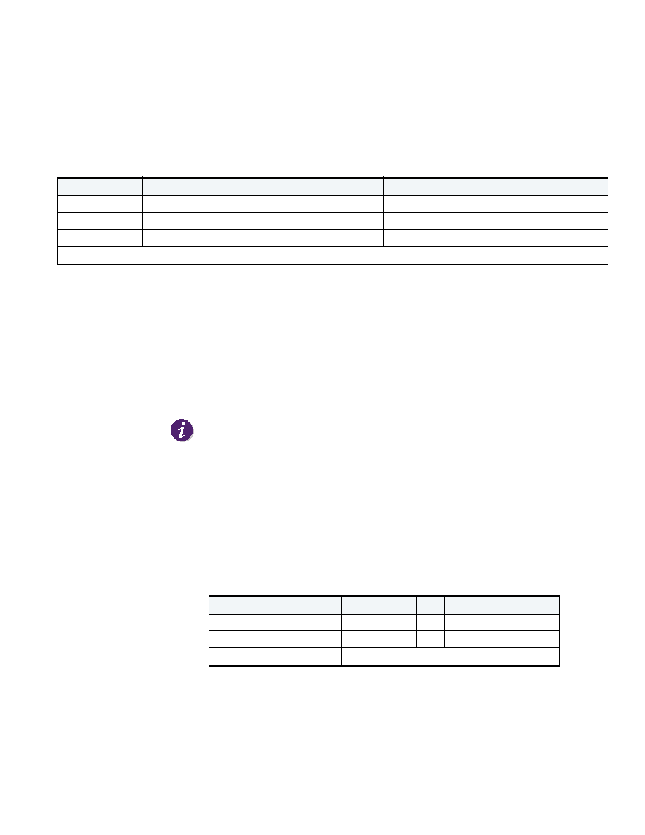
Pin Descriptions Grouped by Function
43
MOTOROLA GENERAL BUSINESS INFORMATION
C5ENPA1-DS/D REV 03
Serial Interface Signals
The Serial interface is a bidirectional two-wire serial bus. It can use one of the following
formats:
�
An 8bit data format followed by an acknowledge bit, which supports transfers at up to
400kbps (low speed).
�
A 16bit IEEE 802.3 MDIO data format with 10bits of addressing, which supports
transfers up to 25MHz (high speed).
The signals and pins are identical for both the high and low speed protocols.
Which of the two data rates used is selected by the state of the PROM interface's SPLD
signal that is asserted while the PROM interface is idle. When SPLD is asserted HI the low
speed serial bus protocol is selected and when SPLD is asserted LOW the MDIO protocol is
selected.
The bus only supports a single master hierarchy that can operate as either a receiver or a
transmitter.
Both SIDA and SICL are bidirectional lines that are connected, through a pull-up resistor, to
a positive supply voltage. When the bus is free, both lines are HIGH. The output stages of
the devices connected to the bus must have either an open-drain or open-collector in
order to perform the wired-AND function required for its arbitration mechanism.
PGNTX
Y7
1
I
PD
I
Initiator bus grant (arbitration)
PIDSEL
Y8
1
PCI
I
Initialization device select
PINTA
Y9
1
PCI
O
Interrupt
TOTAL PINS
50
Table 15 PCI Signals (continued)
SIGNAL NAME
PIN #
TOTAL
TYPE
I/O
SIGNAL DESCRIPTION
Table 16 Serial Interface Signals
SIGNAL NAME
PIN #
TOTAL
TYPE
I/O
SIGNAL DESCRIPTION
SICL
Y5
1
LVTTL
I
PD
/O Serial Clock line
SIDA
Y6
1
LVTTL
I
PD
/O Serial Data line
TOTAL PINS
2
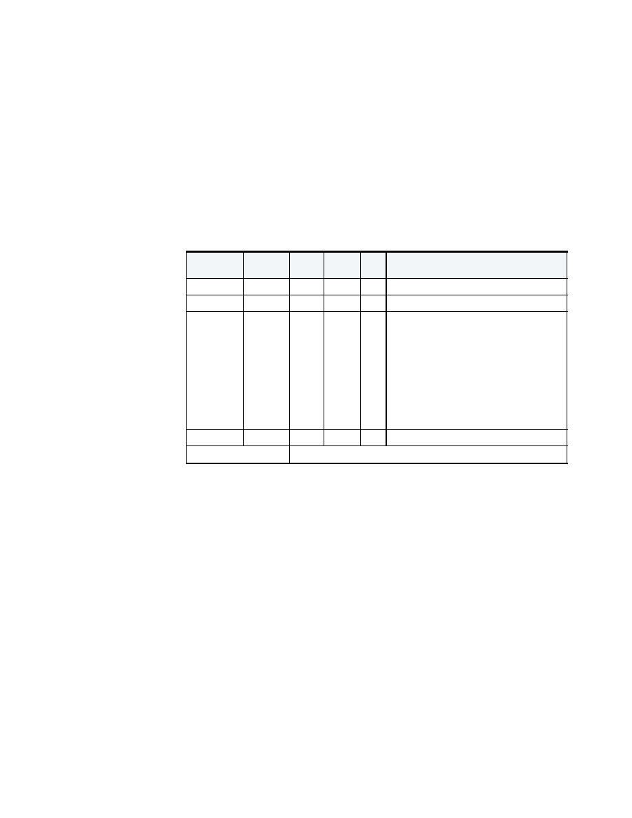
44
CHAPTER 2: SIGNAL DESCRIPTIONS
C5ENPA1-DS/D REV 03
MOTOROLA GENERAL BUSINESS INFORMATION
PROM Interface Signals
The PROM interface is a low speed I/O port that allows the C-5e NP to communicate
through external logic to PROM. The PROM clock is
1
/
2
to
1
/
16
the core clock rate. The
maximum PROM size addressable is 4MBytes, and must use a "by 16" part. The PROM
signals are listed in
Table 17
.
Figure 5
shows the connections between the PROM Interface and external board logic.
The application is required to provide an external shift register with parallel-in and
parallel-out capabilities, and a parallel load register. Both devices should be
positive-edge-triggered and perform a parallel load whenever SPLD is asserted. When
SPLD is deasserted the shift register shifts.
Table 17 PROM Interface Signals
SIGNAL
NAME
PIN #
TOTAL
TYPE
I/O
SIGNAL DESCRIPTION
SPDO
Y1
1
LVTTL
O
Serial Data Out
SPDI
Y2
1
LVTTL
I
PD
Serial Data In
SPLD
Y3
1
LVTTL
O
When load is asserted on a positive clock
edge, the external logic performs a parallel
load. On each positive clock edge when
load is de-asserted, the shift registers shift.
When the PROM interface is idle:
�
If SPLD is asserted HI it indicates low
speed serial protocol,
�
If asserted LOW it indicates MDIO serial
protocol.
SPCK
Y4
1
LVTTL
O
Clock
TOTAL PINS
4

Pin Descriptions Grouped by Function
45
MOTOROLA GENERAL BUSINESS INFORMATION
C5ENPA1-DS/D REV 03
Figure 5 PROM Interface Diagram
The PROM interface operates in the following manner (Note that two accesses are
piplined together to execute one 32-bit fetch). The steps are shown in
Figure 6
.
1 The PROM_ADDR is loaded into the network processor internal shift register.
2 The PROM_ADDR is shifted into the external shift register for 22 SPCLK cycles.
3 SPLD is asserted for one SPCLK cycle, loading the PROM_ADDR into the external
presentation register.
4 SPLD is deasserted for 22 SPCLK cycles. The PROM presents the first 16bit PROM_DATA.
At the same time, the next PROM_ADDR is shifted into the external shift register.
5 SPLD is asserted for one SPCLK cycle, loading the PROM_ADDR into the external
presentation register and the first PROM_DATA into the external shift register.
6 SPLD is deasserted for 22 SPCLK cycles, shifting the first PROM_DATA into the network
processor internal shift register.
7 SPLD is asserted for one SPCLK cycle, loading the first PROM_DATA into the network
processor PROM_RETURN_DATA register and the second PROM_DATA into the
external shift register.
External Logic
PROM_ADDR<21:1>
15
15
16
PROM _H_Word
C-5e Network Processor
PROM Clock Gen.
31
21
21
6
1
0
PROM _Return_Data
PROM Sequencer
21
0
0
CE
SPCLK
SPLD
SPDO
SPDI
Internal Shift
Register
PROM_ADDR<21:1>
CE
PROM _LO_Word
21
6 0
21
0
21
1
PROM
PROM_Data
16
External Shift
Register
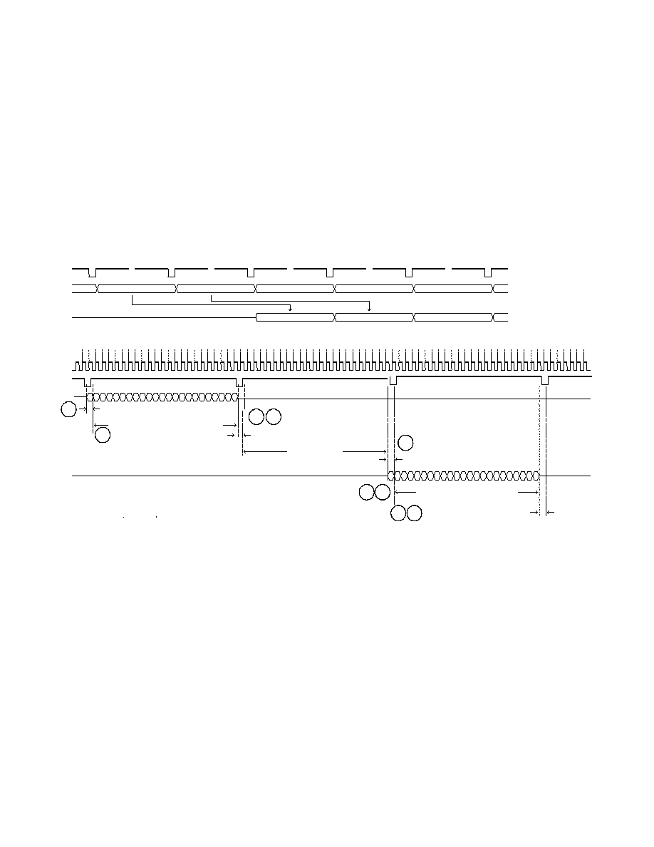
46
CHAPTER 2: SIGNAL DESCRIPTIONS
C5ENPA1-DS/D REV 03
MOTOROLA GENERAL BUSINESS INFORMATION
8 SPLD is deasserted for 22 SPCLK cycles, shifting the second PROM_DATA into the
network processor internal shift register.
9 SPLD is asserted for one SPCLK cycle, loading the second PROM_DATA into the
network processor PROM_RETURN_DATA register.
Figure 6 PROM Interface Timing Outline
SPCLK
SPLD
1
2
4
5
6
7
8
9
11
10
12 13 14 15 16 17 18 19 20 21 22 23 1
2
3
4
5
6
7
8
9
10 11 12 13 14 15 16 17 18 19 20 21 22 23 1
2
3
4
5
6
7
8
9
10 11 12 13 14 15 16 17 18
20
19
21 22 23 1
2
3
4
5
6
7
x
A
20
A
19
A
18
SPDTO
A
17
A
16
A
15
A
14
A
13
A
12
A
11
A
10
A
9
A
8
A
7
A
6
A
5
A
4
A
3
A
2
A
1
A
0
CE
The PROM_ADDR is loaded into the
C-5's internal shift register.
The PROM_ADDR is shifted into
the external shift register.
(SPCLK Rising Edge used for shifting)
The PROM_ADDR is loaded into the
external presentation register.
The PROM_DATA is
presenting.
The PROM_DATA is loaded into the
external shift register.
The PROM_DATA is shifted into the C-5's
Internal shift register.
The PROM_DATA is loaded into the C-5's
internal PROM_RETURN_DATA register.
SPDTI
x
D
15
D
14
D
13
D
12
D
11
D
10
D
9
D
8
D
7
D
6
D
5
D
4
D
3
D
2
D
1
D
0
x
x
x
x
x
x
XP PROM Interface outline
XP PROM Interface detail
SPLD
SPDTO
SPDTI
Q<
Q<
A1
A2
Q<
Q<
`
A3
A4
A5
D1
D2
D3
D1
D2
A1
A2
A3
A4
1
2
3
4
5
6
7
8
9

Pin Descriptions Grouped by Function
47
MOTOROLA GENERAL BUSINESS INFORMATION
C5ENPA1-DS/D REV 03
General System Interface Signal
Table 18
provides the signal for the Executive Processor reset power status and I/O clock.
The C-5e NP can be powered up with the XP either running or with the XP in reset mode
similar to the CPs. When the XP remains in reset mode, an external host can be used to
control the initialization of the C-5e NP.
Table 18 General System Interface Signal
SIGNAL NAME
PIN #
TOTAL
TYPE
I/O
SIGNAL DESCRIPTION
XPUHOT
W8
1
LVTTL
I
PD
Sample at Power On Reset determines if the XP RISC Core is held in reset. Low
equals reset and High equals active. During normal operation, this is an
external interrupt.
TOTAL PINS
1

48
CHAPTER 2: SIGNAL DESCRIPTIONS
C5ENPA1-DS/D REV 03
MOTOROLA GENERAL BUSINESS INFORMATION
Fabric Processor Interface
Signals
The FP has logical signal interfaces: a receive data interface and a transmit data interface,
each with its own control, data, and clock signals. The interface has the following
characteristic:
The interface clocks FRXCLK and FTXCLK can have a different frequency from the core
C-5e NP clock frequency. The FP supports a fabric interface frequency from 10MHz to
125MHz.
FRXCLK and FTXCLK can be independent of each other; typically they have the same
frequency, but are allowed to be skewed relative to each other.
Each data bus can be configured for widths of 8 (data bits 7:0 are used), 16 (bits 15:0), or
32 (bits 31:0). In 8bit mode, data bits 31:8 are unused. In 16bit mode, data bits 31:16 are
unused.
The following tables list the Fabric Interface pin mappings:
�
Utopia1, Utopia2, Utopia3 ATM Mode mappings
are listed in
Table 20
�
Utopia1, Utopia2, Utopia3 PHY Mode mappings
are listed in
Table 21
�
PRIZMA Mode mappings
are listed in
Table 22
(PRIZMA protocol is a subset of Utopia3
PHY)
Table 19 Fabric Interface Signals
SIGNAL NAME
PIN #
TOTAL
TYPE
I/O
SIGNAL DESCRIPTION
FIN0 - FIN31
AE12, AD12, AC12, AJ11, AH11, AG11,AF11,
AE11, AD11, AC11, AJ10, AG10, AF10, AD10,
AC10, AJ9, AH9, AG9, AF9, AE9, AD9, AC9, AJ8,
AH8, AG8, AF8, AE8, AD8, AC8, AJ7, AH7, AG7
32
LVTTL
I
PD
Fabric Data Bus In
FOUT0 - FOUT31
AJ18, AH18, AG18, AE18, AD18, AC18, AJ17,
AH17, AF17, AE17, AD17, AC17, AJ16, AH16,
AG16, AF16, AE16, AD16, AC16, AJ15, AG15,
AF15, AD15, AC15, AJ14, AH14, AG14, AF14,
AE14, AD14, AC14, AJ13
32
LVTTL
O
Fabric Data Bus Out
FRXCLK
AC6
1
LVTTL
I
PD
Receive Clock
FTXCLK
AG12
1
LVTTL
I
PD
Transmit Clock
FRXCTL0 - FRXCTL6
AE7, AD7, AC7, AJ6, AG6, AF6, AD6
7
LVTTL
I
PD
, O Receive Control Signals
FTXCTL0 - FTXCTL6
AH13, AF13, AE13, AD13, AC13, AJ12, AH12
7
LVTTL
I
PD
, O Transmit Control Signals
TOTAL PINS
80

Pin Descriptions Grouped by Function
49
MOTOROLA GENERAL BUSINESS INFORMATION
C5ENPA1-DS/D REV 03
�
Power X(CSIX-L0) Mode mappings are listed in
Table 23
�
CSIX-L1 Mode mappings are listed in
Table 24
When configuring two C-5e network processors back-to-back using the Fabric Port, set
up the transmit side of each C-5e network processor in Utopia ATM mode and the receive
side of each C-5e network processor in Utopia PHY mode.
Table 20 Utopia1*, 2*, 3 ATM Mode, C-5e Network Processor to Fabric Interface Pin Mapping
RECEIVE SIGNALS
TRANSMIT SIGNALS
C-5E NETWORK
PROCESSOR
I/O
UTOPIA
NOTE
C-5E NETWORK
PROCESSOR
I/O
UTOPIA
NOTE
FRXCTL0
Output
RxEnb*
Pullup or No
Connection
FTXCTL0
Output
TxEnb*
Pullup or No
Connection
FRXCTL1
Input
RxClav
FTXCTL1
Input
TxClav
FRXCTL2
Input
RxSOC
FTXCTL2
Output
TxSOC
FRXCTL3
Input
n/a
FTXCTL3
Input
n/a
FRXCTL4
Input
n/a
FTXCTL4
Input
n/a
FRXCTL5
Input
n/a
FTXCTL5
Input
n/a
FRXCTL6
Input
RxPrty
FTXCTL6
Output
TxPrty
*
Cell size must be 4Byte aligned. Both RxEnb and TxEnb are Active Low.
Table 21 Utopia1*, 2*, 3 PHY Mode, C-5e Network Processor to Fabric Interface Pin Mapping
RECEIVE SIGNALS
TRANSMIT SIGNALS
C-5E NETWORK
PROCESSOR
I/O
UTOPIA
NOTE
C-5E NETWORK
PROCESSOR
I/O
UTOPIA
NOTE
FRXCTL0
Input
TxEnb*
Pullup
FTXCTL0
Input
RxEnb*
Pullup
FRXCTL1
Output
TxClav
No Connection
FTXCTL1
Output
RxClav
No Connection
FRXCTL2
Input
TxSOC
FTXCTL2
Output
RxSOC
FRXCTL3
Input
n/a
FTXCTL3
Input
n/a
FRXCTL4
Input
n/a
FTXCTL4
Input
n/a
FRXCTL5
Input
n/a
FTXCTL5
Input
n/a
FRXCTL6
Input
TxPrty
FTXCTL6
Output
RxPrty
*
Cell size must be 4Byte aligned. Both TxEnb and RxEnb are Active Low.

50
CHAPTER 2: SIGNAL DESCRIPTIONS
C5ENPA1-DS/D REV 03
MOTOROLA GENERAL BUSINESS INFORMATION
For the CSIX-L1 Mode, VDDF= 2.5V.
Table 22 PRIZMA Mode, C-5e Network Processor to Fabric Interface Pin Mapping
RECEIVE SIGNALS
TRANSMIT SIGNALS
C-5E NETWORK
PROCESSOR
I/O
UTOPIA
NOTE
C-5E NETWORK
PROCESSOR
I/O
UTOPIA
NOTE
FRXCTL0
Input
TxEnb*
Not connected to
fabric.
FTXCTL0
Input
RxEnb*
Not connected to
fabric.
FRXCTL1
Output
TxClav
No connection
FTXCTL1
Output
RxClav
No Connection
FRXCTL2
Input
TxSOP
FTXCTL2
Output
RxSOP
FRXCTL3
Input
n/a
FTXCTL3
Input
n/a
FRXCTL4
Input
n/a
FTXCTL4
Input
n/a
FRXCTL5
Input
n/a
FTXCTL5
Input
n/a
FRXCTL6
Input
TxPrty
Optional
FTXCTL6
Output
RxPrty
Optional
*
Both TxEnb and RxEnb are Active Low.
Table 23 Power X(CSIX-L0) Mode, C-5e Network Processor to Fabric Interface Pin Mapping
RECEIVE SIGNALS
TRANSMIT SIGNALS
C-5E NETWORK
PROCESSOR
I/O
POWER X
NOTE
C-5E NETWORK
PROCESSOR
I/O
POWER X
NOTE
FRXCTL0
Input
RxCtrl[0]
FTXCTL0
Output
TxCtrl[0]
FRXCTL1
Input
RxCtrl[1]
FTXCTL1
Output
TxCtrl[1]
FRXCTL2
Input
RxCtrl[2]
FTXCTL2
Output
TxCtrl[2]
FRXCTL3
Input
RxPrty[3]
FTXCTL3
Output
TxPrty[3]
FRXCTL4
Input
RxPrty[2]
FTXCTL4
Output
TxPrty[2]
FRXCTL5
Input
RxPrty[1]
FTXCTL5
Output
TxPrty[1]
FRXCTL6
Input
RxPrty[0]
FTXCTL6
Output
TxPrty[0]
Pin Descriptions Grouped by Function
51
MOTOROLA GENERAL BUSINESS INFORMATION
C5ENPA1-DS/D REV 03
Table 24 CSIX-L1 Mode, C-5e Network to Fabric Interface Pin Mapping
FPRX SIGNALS
FPTX SIGNALS
C-5E NP
I/O
CSIX-L1
NOTE
C-5E NP
I/O
CSIX-L1
NOTE
FRxCTL0
Input
n/a
FTxCTL0
Input
n/a
FRxCTL1
Input
n/a
FTxCTL1
Input
n/a
FRxCTL2
Input
TxSOF
FTxCTL2
Output
RxSOF
FRxCTL3
Input
n/a
FTxCTL3
Input
n/a
FRxCTL4
Input
n/a
FTxCTL4
Input
n/a
FRxCTL5
Input
n/a
FTxCTL5
Input
n/a
FRxCTL6
Input
TxPrty
FTxCTL6
Output
RxPrty

52
CHAPTER 2: SIGNAL DESCRIPTIONS
C5ENPA1-DS/D REV 03
MOTOROLA GENERAL BUSINESS INFORMATION
BMU SDRAM Interface
Signals
The BMU and SDRAM interface signals are described in
Table 25
.
The BMU is designed to support SDRAM devices with 12 address lines. All 139 data lines
and all 12 address lines must be connected to the SDRAM in order for the BMU to be able
to read and write external SDRAM properly.
Table 25 BMU SDRAM Interface Signals
SIGNAL NAME
PIN #
TOTAL
TYPE
I/O
SIGNAL DESCRIPTION
MD0 - MD129
U23, U22, U21, T29, T28, T27, T26,
T25, T24, T23, T22, T21, R29, R28,
R27, R26, R25, R24, R23, R22, R21,
P29, P28, P26, P25, P24, P22, P21,
N29, N27, N26, N25, N23, N22, N21,
M29, M28, M27, M26, M25, M24,
M23, M22, M21, L29, L28, L27, L26,
L25, L24, L23, L22, L21, K29, K28,
K26, K25, K24, K22, K21, J29, J27,
J26, J25, J23, J22, J21, H29, H28,
H27, H26, H25, H24, H23, H22, H21,
G29, G28, G27, G26, G25, G24, G23,
G22, G21, F29, F28, F26, F25, F24,
F22, F21, E29, E27, E26, E25, E23,
E22, E21, D29, D28, D27, D26, D25,
D24, D23, D22, D21, C29, C28, C26,
C25, C24, C22, C21, B29, B27, B26,
B25, B23, B22, B21, A29, A28, A27,
A26, A25, A24, A23, A22
130
LVTTL
I
PD
/O Data Lines In
MDECC0 - MDECC8 E19, F19, G19, A20, C20, D20, F20,
G20, A21
9
LVTTL
I
PD
/O Stored as data, ECC bits
MA0 - MA11
B16, C16, D16, E16, F16, G16, A17,
B17, D17, E17, F17, G17
12
LVTTL
O
PD
Address Outputs: A0-A11 are sampled during the
ACTIVE command and READ/WRITE to select one
location out of the memory array in the respective
bank. The address inputs also provide the
op-code during a LOAD MODE REGISTER
command
MBA0 - MBA1
E18, C18
2
LVTTL
O
PD
Bank Address Outputs: BA0 and BA1 define which
bank the ACTIVE, READ, WRITE or PRECHARGE
command is being applied
MCASX
D19
1
LVTTL
O
PD
Command Outputs: MRASX, MCASX, MWEX and
MCSX define the command being entered.
NOTE:
MCSX is considered part of the command
code.

Pin Descriptions Grouped by Function
53
MOTOROLA GENERAL BUSINESS INFORMATION
C5ENPA1-DS/D REV 03
MRASX
C19
1
LVTTL
O
PD
Command Outputs: MRASX, MCASX, MWEX and
MCSX define the command being entered. MCSX
is considered part of the command code.
MWEX
B19
1
LVTTL
O
PD
Command Outputs: MRASX, MCASX, MWEX and
MCSX define the command being entered. MCSX
is considered part of the command code.
MCSX
A19
1
LVTTL
O
PD
Chip Select: MCSX enables (registered LOW) and
disables (registered HIGH) the command decoder.
All commands are masked when MCSX is
registered HIGH. MCSX provides the external bank
selection on systems with multiple banks. MCSX is
considered part of the command code.
MDQM
MDQML
G18
F18
1
1
LVTTL
LVTTL
O
PD
O
PD
Input/Output Mask: MDQM is an input mask
signal for write accesses and an output enable
signal for read accesses. Input data is masked
when MDQM is sampled HIGH during a WRITE
cycle. The output buffers are placed in a high Z
state (two-clock latency) when MDQM is sampled
HIGH during the READ cycle.
NOTE: MDQML is an identical copy of MDQM
used to drive the loading on SDRAM
configurations with 2 DQM pins.
MDCLK
B18
1
LVTTL
I
PD
Clock: MDCLK is driven by the system clock. All
SDRAM input signals are sampled on the positive
edge of the MDCLK. MDCLK also increments the
internal burst counter and controls the output
registers.
TOTAL PINS
160
Table 25 BMU SDRAM Interface Signals (continued)
SIGNAL NAME
PIN #
TOTAL
TYPE
I/O
SIGNAL DESCRIPTION
54
CHAPTER 2: SIGNAL DESCRIPTIONS
C5ENPA1-DS/D REV 03
MOTOROLA GENERAL BUSINESS INFORMATION
TLU SRAM Interface
Signals
The TLU SRAM interface supports up to 128MBytes of SRAM at frequencies to 133MHz
using LVTTL signaling levels (in single bank-mode only) and SRAM technologies up to
64Mbits. The TLU SRAM interface signals are described in
Table 26
.
Table 26 TLU SRAM Interface Signals
SIGNAL NAME
PIN #
TOTAL
TYPE
I/O
SIGNAL DESCRIPTION
TD0 - TD63
G6, G7, G8, G9, G10, H1, H2, H3, H4, H5, H6, H7, H8,
H9, J1, J3, J4, J5, J7, J8, J9, K1, K2, K4, K5, K6, K8, K9,
L1, L2, L3, L4, L5, L6, L7, L8, L9, M1, M2, M3, M4,
M5, M6, M7, M8, M9, N1, N3, N4, N5, N7, N8, N9,
P1, P2, P4, P5, P6, P8, P9, R6, R7, R8, R9
64
LVTTL
I
PD
/O TLU Memory Data
TA0 - TA21
T1, U1, U3, U4, U5, U7, U8, U9, V1, V2, V4, V5, V6,
V8, V9, W1, W2, W3, W4, W5, W6, W7
22
LVTTL
O
PD
TLU Memory Address
TPAR0 - TPAR3
R2, R3, R4, R5
4
LVTTL
I
PD
/O Word Data Parity (i.e. TPAR0 across
TD15:0)
TCE0X - TCE3X
T2, T3, T4, T5
4
LVTTL
O
PD
TLU Memory Chip Enable
TWE0X - TWE3X
T6, T7, T8, T9
4
LVTTL
O
PD
TLU Memory Write Enable
TCLKI
R1
1
LVTTL
I
PD
TLU Clock Input
TOTAL PINS
99
Pin Descriptions Grouped by Function
55
MOTOROLA GENERAL BUSINESS INFORMATION
C5ENPA1-DS/D REV 03
QMU SRAM (Internal
Mode) Interface Signals
The QMU signals are described in
Table 27
.
Table 27 QMU SRAM (Internal Mode) Interface Signals
SIGNAL NAME
PIN #
TOTAL
TYPE
I/O
SIGNAL DESCRIPTION
QA0 - QA16
C8, B8, A8, F9, E9, D9, C9, B9, A9, F10, D10, C10,
A10, G11, F11, E11, D11
17
LVTTL
O
Address [16:0]
QD0 - QD31
G1, F1, E1, D1, C1, B1, G2, F2, D2, C2, A2, G3, E3,
D3, B3, A3, G4, F4, E4, D4, C4, B4, A4, G5, F5, E5,
D5, C5, B5, A5, F6, D6
32
LVTTL
I
PD
/O Data
QDQPAR
C11
1
LVTTL
I
PD
nc
QARDY
E8
1
LVTTL
I
PD
nc
QNQRDY
D8
1
LVTTL
I
PD
nc
QWEX
C6
1
LVTTL
O
Write Enable
QBCLKO
A6
1
LVTTL
O
nc
QBCLKI
E7
1
LVTTL
I
PD
nc
QACLKO
D7
1
LVTTL
O
nc
QACLKI
B7
1
LVTTL
I
PD
Input Clock
QDPL
A7
1
LVTTL
I
PD
/O Data Parity Low
QDPH
F8
1
LVTTL
I
PD
/O Data Parity High
TOTAL PINS
59

56
CHAPTER 2: SIGNAL DESCRIPTIONS
C5ENPA1-DS/D REV 03
MOTOROLA GENERAL BUSINESS INFORMATION
QMU to Q-5 TMC (External
Mode) Interface Signals
The QMU to Q-5 Traffic Management Coprocessor (TMC) signals are described in
Table 28
.
Table 28 QMU to Q-5 (External Mode) Interface Signals
SIGNAL NAME
PIN #
TOTAL
TYPE
I/O
SIGNAL DESCRIPTION
QA0 - QA15
C8, B8, A8, F9, E9, D9, C9, B9, A9, F10, D10,
C10, A10, G11, F11, E11
16
LVTTL
O
Enqueue Data [8:23]
QA16
D11
1
LVTTL
O
Enqueue Parity
QD0 - QD23
G1, F1, E1, D1, C1, B1, G2, F2, D2, C2, A2, G3,
E3, D3, B3, A3, G4, F4, E4, D4, C4, B4, A4, G5
24
LVTTL
I
PD
Dequeue Data [0:23]
QD24 - QD31
F5, E5, D5, C5, B5, A5, F6, D6
8
LVTTL
I
PD
Enqueue Data [0:7]
QDQPAR
C11
1
LVTTL
I
PD
Dequeue Parity
QARDY
E8
1
LVTTL
I
PD
Dequeue Ack Ready
QNQRDY
D8
1
LVTTL
I
PD
Enqueue Ready
QWEX
C6
1
LVTTL
O
Dequeue Ready
QBCLKO
A6
1
LVTTL
O
Output ClockB
QBCLKI
E7
1
LVTTL
I
PD
Input ClockB
QACLKO
D7
1
LVTTL
O
Output ClockA
QACLKI
B7
1
LVTTL
I
PD
Input ClockA
QDPL
A7
1
LVTTL
O
Dequeue Ack [0]
QDPH
F8
1
LVTTL
O
Dequeue Ack [1]
TOTAL PINS
59

Pin Descriptions Grouped by Function
57
MOTOROLA GENERAL BUSINESS INFORMATION
C5ENPA1-DS/D REV 03
Power Supply Signals
Power supply, and ground signals are described in
Table 29
.
Table 29 Power Supply Signals
SIGNAL NAME
PIN #
TOTAL
TYPE
SIGNAL DESCRIPTION
VDD
J13, J15, J17, J19, K12, K14, K16, K18, L11, L13, L15,
L17, L19, M12, M14, M16, M18, N13, N15, N17, N19,
P12, P14, P16, P18, R11, R13, R15, R17, R19, T12, T14,
T16, T18, U11, U13, U15, U17, U19, V12, V14, V16,
V18, W11, W13, W15, W17, W19, Y12, Y14, Y16, Y18,
AA11, AA13, AA15, AA17, AA19,
57
P
Core Supply Voltage (1.2V Input)
VDD33
B20, B28, C13, C17, C23, E15, F23, F27, H12, H14,
H16, H18, H20, J28, K20, K23, M20, N24, P20, P27,
T20, U28, V20, V23, Y20, AA6, AA24, AB3, AB10,
AB18, AB20, AB27, AE24, AF3, AF27, AH2, AH20,
AH28
38
P
I/O Supply Voltage (3.3V Input)
GND
B6, B15, B24, C3, C27, D12, D18, E2, E6, E10, E20, E24,
E28, H11, H13, H15, H17, H19, J6, J10, J12, J14, J16,
J18, J20, J24, K3, K11, K13, K15, K17, K19, K27, L10,
L12, L14, L16, L18, L20, M11, M13, M15, M17, M19,
N2, N10, N12, N14, N16, N18, N20, N28, P7, P11, P13,
P15, P17, P19, P23, R10, R12, R14, R16, R18, R20, T11,
T13, T15, T17, T19, U6, U10, U12, U14, U16, U18, U20,
U24, V3, V11, V13, V15, V17, V19, V27, W10, W12,
W14, W16, W18, W20, Y11, Y13, Y15, Y17, Y19, AA2,
AA10, AA12, AA14, AA16, AA18, AA20, AA28, AB7,
AB11, AB13, AB15, AB17, AB19, AB23, AE2, AE10,
AE20, AE28, AF7, AF12, AF18, AF23, AH6, AH15,
AH24
122
P
Ground
VDDF
AB12, AB14, AB16, AE6, AE15, AG13, AG17, AH10
8
P
Fabric I/O supply (3.3 or 2.5V)
VDDT
B2, B10, C7, F3, F7, H10, J2, J11, K7, K10, M10, N6,
N11, P3, P10, T10, U2, V7, V10, Y10
20
P
TLU and QMU I/O supply (3.3V)
TOTAL PINS
245

58
CHAPTER 2: SIGNAL DESCRIPTIONS
C5ENPA1-DS/D REV 03
MOTOROLA GENERAL BUSINESS INFORMATION
Test Signals
Test signals are described in
Table 30
.
During JTAG, SCLK and SCLKX must remain as differential inputs.
No Connection Pins
No connection pins are listed in
Table 31
.
Table 30 Miscellaneous Test Signals For JTAG, Scan, and Internal Test Routines
SIGNAL NAME
PIN #
TOTAL
TYPE
I/O
SIGNAL DESCRIPTION
JTCK
C15
1
LVTTL
I
PD
Test Clock
JTMS
A14
1
LVTTL
I
PD
Test Mode Select. High selects modes
as defined in the IEEE 1149.1 JTAG
specification.
JTRSTX
A12
1
LVTTL
I
PD
Test Reset (low active)
JTDI
B14
1
LVTTL
I
PD
Test Data In
JTDO
A13
1
LVTTL
O
Test Data Out
JHIGHZ
B13
1
LVTTL
I
PD
Turns off all output drivers when High
JCLKBYP
C14
1
LVTTL
I
PD
1X or 2X Clock Mode Select. Low
selects 1X, High selects 2X.
JSE
D15
1
LVTTL
I
PD
Scan Enable. High enables scan test.
JS00-JS05
D14, A16, D13, C12, A15, B12
6
LVTTL
O
Scan Out Pins
TOTAL PINS
14
Table 31 No Connection Pins
SIGNAL NAME
PIN #
TOTAL
TYPE
I/O
SIGNAL DESCRIPTION
NC3 - NC5
B11, A11, A18
3
nc
I
PD
/O Reserved for future functionality
TOTAL PINS
3
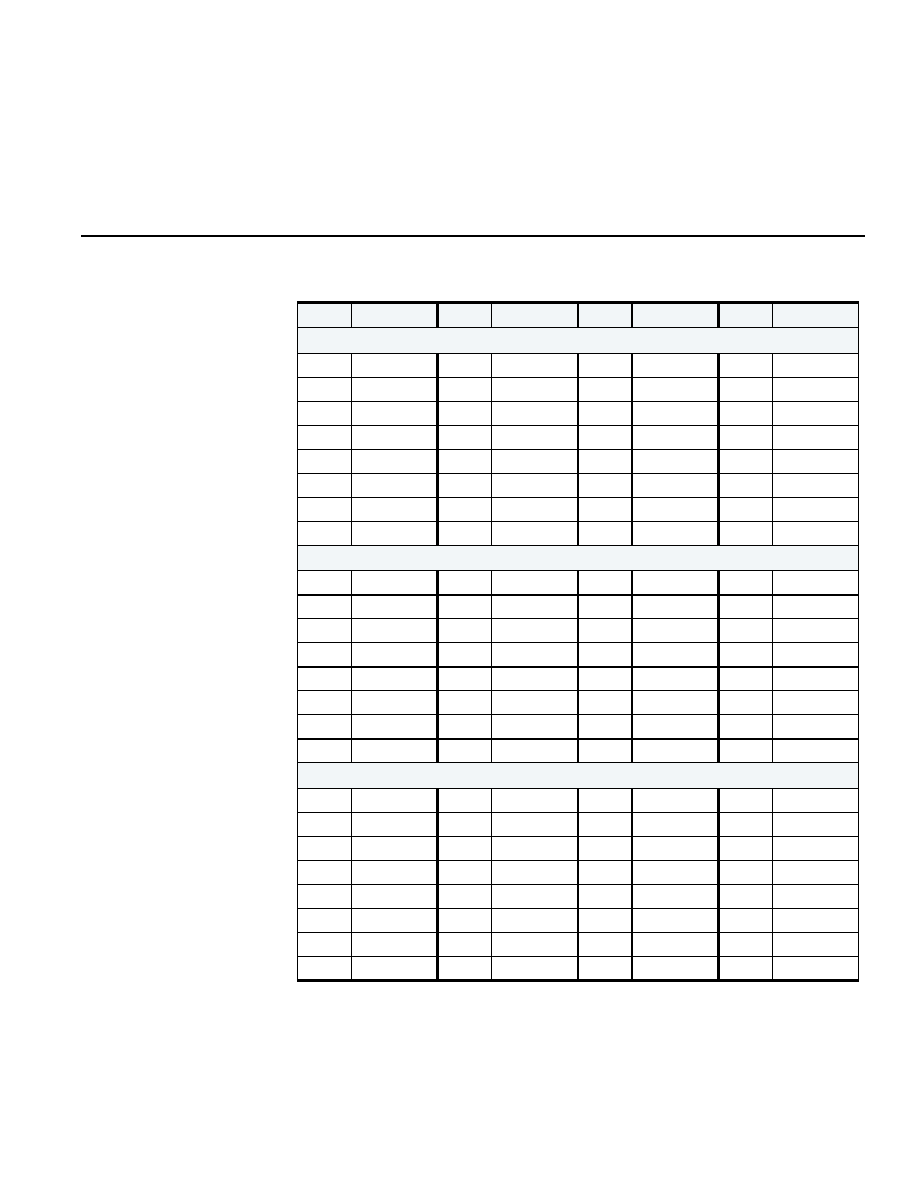
Signals Grouped by Pin Number
59
MOTOROLA GENERAL BUSINESS INFORMATION
C5ENPA1-DS/D REV 03
Signals Grouped by Pin
Number
The C-5e NP signals are listed by pin number in
Table 32
.
Table 32 Signals Listed by Pin Number
PIN
FUNCTION
PIN
FUNCTION
PIN
FUNCTION
PIN
FUNCTION
A 1-29
A1
Not present
A9
QA8
A17
MA6
A25
MD126
A2
QD10
A10
QA12
A18
NC5
A26
MD125
A3
QD15
A11
NC4
A19
MCSX
A27
MD124
A4
QD22
A12
JTRSTX
A20
MDECC3
A28
MD123
A5
QD29
A13
JTDO
A21
MDECC8
A29
MD122
A6
QBCLKO
A14
JTMS
A22
MD129
A7
QDPL
A15
JSO4
A23
MD128
A8
QA2
A16
JSO1
A24
MD127
B 1-29
B1
QD5
B9
QA7
B17
MA7
B25
MD118
B2
VDDT
B10
VDDT
B18
MDCLK
B26
MD117
B3
QD14
B11
NC3
B19
MWEX
B27
MD116
B4
QD21
B12
JSO5
B20
VDD33
B28
VDD33
B5
QD28
B13
JHIGHZ
B21
MD121
B29
MD115
B6
GND
B14
JTDI
B22
MD120
B7
QACLKI
B15
GND
B23
MD119
B8
QA1
B16
MA0
B24
GND
C 1-29
C1
QD4
C9
QA6
C17
VDD33
C25
MD111
C2
QD9
C10
QA11
C18
MBA1
C26
MD110
C3
GND
C11
QDQPAR
C19
MRASX
C27
GND
C4
QD20
C12
JSO3
C20
MDECC4
C28
MD109
C5
QD27
C13
VDD33
C21
MD114
C29
MD108
C6
QWEX
C14
JCLKBYP
C22
MD113
C7
VDDT
C15
JTCK
C23
VDD33
C8
QA0
C16
MA1
C24
MD112

60
CHAPTER 2: SIGNAL DESCRIPTIONS
C5ENPA1-DS/D REV 03
MOTOROLA GENERAL BUSINESS INFORMATION
D 1-29
D1
QD3
D9
QA5
D17
MA8
D25
MD103
D2
QD8
D10
QA10
D18
GND
D26
MD102
D3
QD13
D11
QA16
D19
MCASX
D27
MD101
D4
QD19
D12
GND
D20
MDECC5
D28
MD100
D5
QD26
D13
JSO2
D21
MD107
D29
MD99
D6
QD31
D14
JSO0
D22
MD106
D7
QACLKO
D15
JSE
D23
MD105
D8
QNQRDY
D16
MA2
D24
MD104
E 1-29
E1
QD2
E9
QA4
E17
MA9
E25
MD95
E2
GND
E10
GND
E18
MBA0
E26
MD94
E3
QD12
E11
QA15
E19
MDECC0
E27
MD93
E4
QD18
E12
CCLK7
E20
GND
E28
GND
E5
QD25
E13
CCLK5
E21
MD98
E29
MD92
E6
GND
E14
CCLK2
E22
MD97
E7
QBCLKI
E15
VDD33
E23
MD96
E8
QARDY
E16
MA3
E24
GND
F 1-29
F1
QD1
F9
QA3
F17
MA10
F25
MD88
F2
QD7
F10
QA9
F18
MDQML
F26
MD87
F3
VDDT
F11
QA14
F19
MDECC1
F27
VDD33
F4
QD17
F12
CCLK6
F20
MDECC6
F28
MD86
F5
QD24
F13
CCLK4
F21
MD91
F29
MD85
F6
QD30
F14
CCLK1
F22
MD90
F7
VDDT
F15
SCLKX
F23
VDD33
F8
QDPH
F16
MA4
F24
MD89
Table 32 Signals Listed by Pin Number (continued)
PIN
FUNCTION
PIN
FUNCTION
PIN
FUNCTION
PIN
FUNCTION

Signals Grouped by Pin Number
61
MOTOROLA GENERAL BUSINESS INFORMATION
C5ENPA1-DS/D REV 03
G 1-29
G1
QD0
G9
TD3
G17
MA11
G25
MD80
G2
QD6
G10
TD4
G18
MDQM
G26
MD79
G3
QD11
G11
QA13
G19
MDECC2
G27
MD78
G4
QD16
G12
CPREF
G20
MDECC7
G28
MD77
G5
QD23
G13
CCLK3
G21
MD84
G29
MD76
G6
TD0
G14
CCLK0
G22
MD83
G7
TD1
G15
SCLK
G23
MD82
G8
TD2
G16
MA5
G24
MD81
H 1-29
H1
TD5
H9
TD13
H17
GND
H25
MD71
H2
TD6
H10
VDDT
H18
VDD33
H26
MD70
H3
TD7
H11
GND
H19
GND
H27
MD69
H4
TD8
H12
VDD33
H20
VDD33
H28
MD68
H5
TD9
H13
GND
H21
MD75
H29
MD67
H6
TD10
H14
VDD33
H22
MD74
H7
TD11
H15
GND
H23
MD73
H8
TD12
H16
VDD33
H24
MD72
J 1-29
J1
TD14
J9
TD20
J17
VDD
J25
MD63
J2
VDDT
J10
GND
J18
GND
J26
MD62
J3
TD15
J11
VDDT
J19
VDD
J27
MD61
J4
TD16
J12
GND
J20
GND
J28
VDD33
J5
TD17
J13
VDD
J21
MD66
J29
MD60
J6
GND
J14
GND
J22
MD65
J7
TD18
J15
VDD
J23
MD64
J8
TD19
J16
GND
J24
GND
Table 32 Signals Listed by Pin Number (continued)
PIN
FUNCTION
PIN
FUNCTION
PIN
FUNCTION
PIN
FUNCTION
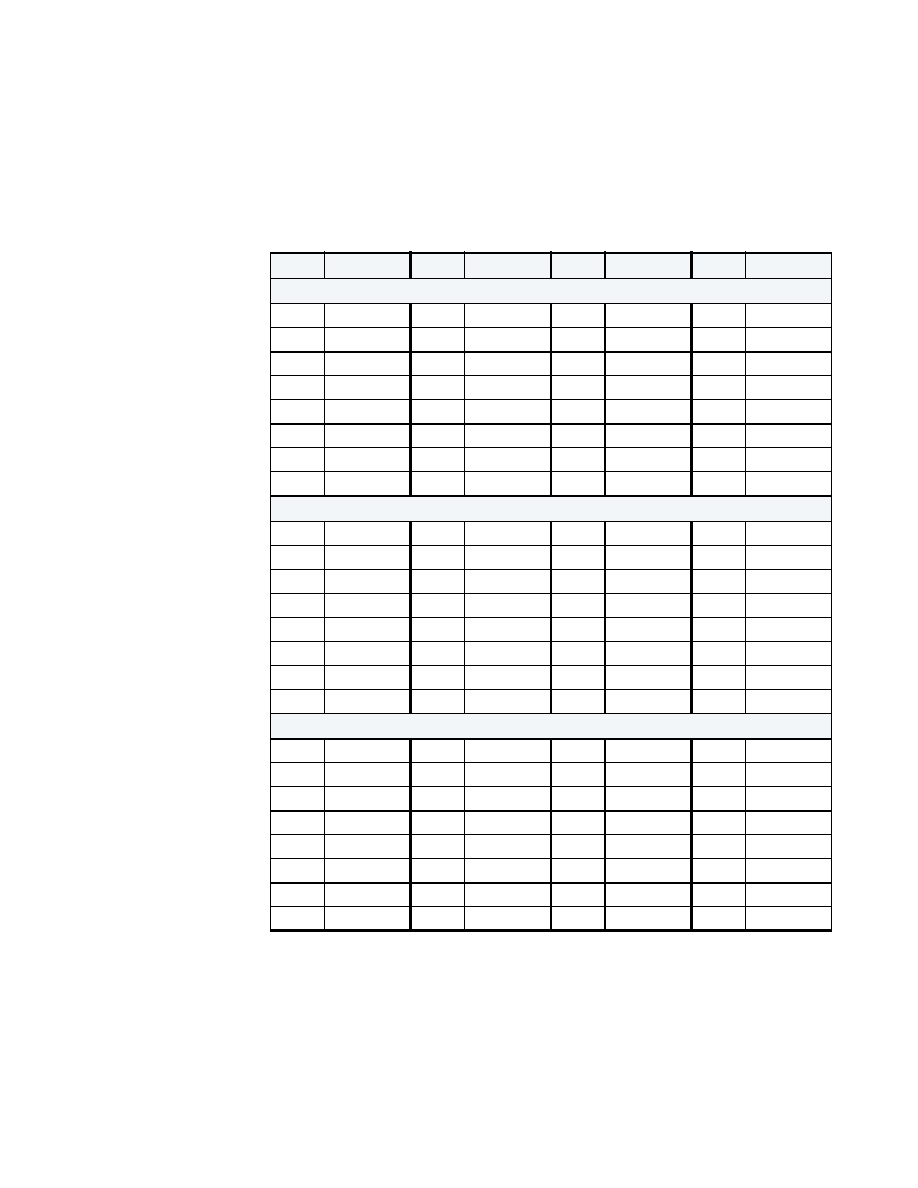
62
CHAPTER 2: SIGNAL DESCRIPTIONS
C5ENPA1-DS/D REV 03
MOTOROLA GENERAL BUSINESS INFORMATION
K 1-29
K1
TD21
K9
TD27
K17
GND
K25
MD56
K2
TD22
K10
VDDT
K18
VDD
K26
MD55
K3
GND
K11
GND
K19
GND
K27
GND
K4
TD23
K12
VDD
K20
VDD33
K28
MD54
K5
TD24
K13
GND
K21
MD59
K29
MD53
K6
TD25
K14
VDD
K22
MD58
K7
VDDT
K15
GND
K23
VDD33
K8
TD26
K16
VDD
K24
MD57
L 1-29
L1
TD28
L9
TD36
L17
VDD
L25
MD48
L2
TD29
L10
GND
L18
GND
L26
MD47
L3
TD30
L11
VDD
L19
VDD
L27
MD46
L4
TD31
L12
GND
L20
GND
L28
MD45
L5
TD32
L13
VDD
L21
MD52
L29
MD44
L6
TD33
L14
GND
L22
MD51
L7
TD34
L15
VDD
L23
MD50
L8
TD35
L16
GND
L24
MD49
M 1-29
M1
TD37
M9
TD45
M17
GND
M25
MD39
M2
TD38
M10
VDDT
M18
VDD
M26
MD38
M3
TD39
M11
GND
M19
GND
M27
MD37
M4
TD40
M12
VDD
M20
VDD33
M28
MD36
M5
TD41
M13
GND
M21
MD43
M29
MD35
M6
TD42
M14
VDD
M22
MD42
M7
TD43
M15
GND
M23
MD41
M8
TD44
M16
VDD
M24
MD40
Table 32 Signals Listed by Pin Number (continued)
PIN
FUNCTION
PIN
FUNCTION
PIN
FUNCTION
PIN
FUNCTION

Signals Grouped by Pin Number
63
MOTOROLA GENERAL BUSINESS INFORMATION
C5ENPA1-DS/D REV 03
N 1-29
N1
TD46
N9
TD52
N17
VDD
N25
MD31
N2
GND
N10
GND
N18
GND
N26
MD30
N3
TD47
N11
VDDT
N19
VDD
N27
MD29
N4
TD48
N12
GND
N20
GND
N28
GND
N5
TD49
N13
VDD
N21
MD34
N29
MD28
N6
VDDT
N14
GND
N22
MD33
N7
TD50
N15
VDD
N23
MD32
N8
TD51
N16
GND
N24
VDD33
P 1-29
P1
TD53
P9
TD59
P17
GND
P25
MD24
P2
TD54
P10
VDDT
P18
VDD
P26
MD23
P3
VDDT
P11
GND
P19
GND
P27
VDD33
P4
TD55
P12
VDD
P20
VDD33
P28
MD22
P5
TD56
P13
GND
P21
MD27
P29
MD21
P6
TD57
P14
VDD
P22
MD26
P7
GND
P15
GND
P23
GND
P8
TD58
P16
VDD
P24
MD25
R 1-29
R1
TCLKI
R9
TD63
R17
VDD
R25
MD16
R2
TPAR0
R10
GND
R18
GND
R26
MD15
R3
TPAR1
R11
VDD
R19
VDD
R27
MD14
R4
TPAR2
R12
GND
R20
GND
R28
MD13
R5
TPAR3
R13
VDD
R21
MD20
R29
MD12
R6
TD60
R14
GND
R22
MD19
R7
TD61
R15
VDD
R23
MD18
R8
TD62
R16
GND
R24
MD17
Table 32 Signals Listed by Pin Number (continued)
PIN
FUNCTION
PIN
FUNCTION
PIN
FUNCTION
PIN
FUNCTION

64
CHAPTER 2: SIGNAL DESCRIPTIONS
C5ENPA1-DS/D REV 03
MOTOROLA GENERAL BUSINESS INFORMATION
T 1-29
T1
TA0
T9
TWE3X
T17
GND
T25
MD7
T2
TCE0X
T10
VDDT
T18
VDD
T26
MD6
T3
TCE1X
T11
GND
T19
GND
T27
MD5
T4
TCE2X
T12
VDD
T20
VDD33
T28
MD4
T5
TCE3X
T13
GND
T21
MD11
T29
MD3
T6
TWE0X
T14
VDD
T22
MD10
T7
TWE1X
T15
GND
T23
MD9
T8
TWE2X
T16
VDD
T24
MD8
U 1-29
U1
TA1
U9
TA7
U17
VDD
U25
CPF_6
U2
VDDT
U10
GND
U18
GND
U26
CPF_5
U3
TA2
U11
VDD
U19
VDD
U27
CPF_4
U4
TA3
U12
GND
U20
GND
U28
VDD33
U5
TA4
U13
VDD
U21
MD2
U29
CPF_3
U6
GND
U14
GND
U22
MD1
U7
TA5
U15
VDD
U23
MD0
U8
TA6
U16
GND
U24
GND
V 1-29
V1
TA8
V9
TA14
V17
GND
V25
CPE_6
V2
TA9
V10
VDDT
V18
VDD
V26
CPE_5
V3
GND
V11
GND
V19
GND
V27
GND
V4
TA10
V12
VDD
V20
VDD33
V28
CPE_4
V5
TA11
V13
GND
V21
CPF_2
V29
CPE_3
V6
TA12
V14
VDD
V22
CPF_1
V7
VDDT
V15
GND
V23
VDD33
V8
TA13
V16
VDD
V24
CPF_0
Table 32 Signals Listed by Pin Number (continued)
PIN
FUNCTION
PIN
FUNCTION
PIN
FUNCTION
PIN
FUNCTION

Signals Grouped by Pin Number
65
MOTOROLA GENERAL BUSINESS INFORMATION
C5ENPA1-DS/D REV 03
W 1-29
W1
TA15
W9
PFRAMEX
W17
VDD
W25
CPD_5
W2
TA16
W10
GND
W18
GND
W26
CPD_4
W3
TA17
W11
VDD
W19
VDD
W27
CPD_3
W4
TA18
W12
GND
W20
GND
W28
CPD_2
W5
TA19
W13
VDD
W21
CPE_2
W29
CPD_1
W6
TA20
W14
GND
W22
CPE_1
W7
TA21
W15
VDD
W23
CPE_0
W8
XPUHOT
W16
GND
W24
CPD_6
Y 1-29
Y1
SPDO
Y9
PINTA
Y17
GND
Y25
CPC_3
Y2
SPDI
Y10
VDDT
Y18
VDD
Y26
CPC_2
Y3
SPLD
Y11
GND
Y19
GND
Y27
CPC_1
Y4
SPCK
Y12
VDD
Y20
VDD33
Y28
CPC_0
Y5
SICL
Y13
GND
Y21
CPD_0
Y29
CPB_6
Y6
SIDA
Y14
VDD
Y22
CPC_6
Y7
PGNTX
Y15
GND
Y23
CPC_5
Y8
PIDSEL
Y16
VDD
Y24
CPC_4
AA 1-29
AA1
PSERRX
AA9
PREQX
AA17
VDD
AA25
CPB_2
AA2
GND
AA10
GND
AA18
GND
AA26
CPB_1
AA3
PPERRX
AA11
VDD
AA19
VDD
AA27
CPB_0
AA4
PDEVSELX
AA12
GND
AA20
GND
AA28
GND
AA5
PSTOPX
AA13
VDD
AA21
CPB_5
AA29
CPA_6
AA6
VDD33
AA14
GND
AA22
CPB_4
AA7
PCLK
AA15
VDD
AA23
CPB_3
AA8
PRSTX
AA16
GND
AA24
VDD33
Table 32 Signals Listed by Pin Number (continued)
PIN
FUNCTION
PIN
FUNCTION
PIN
FUNCTION
PIN
FUNCTION

66
CHAPTER 2: SIGNAL DESCRIPTIONS
C5ENPA1-DS/D REV 03
MOTOROLA GENERAL BUSINESS INFORMATION
AB 1-29
AB1
PPAR
AB9
PTRDYX
AB17
GND
AB25
CPA_2
AB2
PCBEX3
AB10
VDD33
AB18
VDD33
AB26
CPA_1
AB3
VDD33
AB11
GND
AB19
GND
AB27
VDD33
AB4
PCBEX2
AB12
VDDF
AB20
VDD33
AB28
CPA_0
AB5
PCBEX1
AB13
GND
AB21
CPA_5
AB29
CP9_6
AB6
PCBEX0
AB14
VDDF
AB22
CPA_4
AB7
GND
AB15
GND
AB23
GND
AB8
PIRDYX
AB16
VDDF
AB24
CPA_3
AC 1-29
AC1
PAD31
AC9
FIN21
AC17
FOUT11
AC25
CP4_3
AC2
PAD30
AC10
FIN14
AC18
FOUT5
AC26
CP3_3
AC3
PAD29
AC11
FIN9
AC19
CP9_5
AC27
CP2_3
AC4
PAD28
AC12
FIN2
AC20
CP8_5
AC28
CP1_4
AC5
PAD27
AC13
FTXCTL4
AC21
CP8_0
AC29
CP0_6
AC6
FRXCLK
AC14
FOUT30
AC22
CP7_0
AC7
FRXCTL2
AC15
FOUT23
AC23
CP6_0
AC8
FIN28
AC16
FOUT18
AC24
CP5_1
AD 1-29
AD1
PAD26
AD9
FIN20
AD17
FOUT10
AD25
CP4_2
AD2
PAD25
AD10
FIN13
AD18
FOUT4
AD26
CP3_2
AD3
PAD24
AD11
FIN8
AD19
CP9_4
AD27
CP2_2
AD4
PAD23
AD12
FIN1
AD20
CP8_4
AD28
CP1_3
AD5
PAD22
AD13
FTXCTL3
AD21
CP7_6
AD29
CP0_5
AD6
FRXCTL6
AD14
FOUT29
AD22
CP6_6
AD7
FRXCTL1
AD15
FOUT22
AD23
CP5_6
AD8
FIN27
AD16
FOUT17
AD24
CP5_0
Table 32 Signals Listed by Pin Number (continued)
PIN
FUNCTION
PIN
FUNCTION
PIN
FUNCTION
PIN
FUNCTION
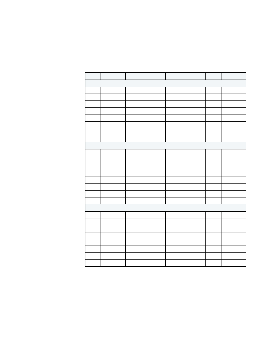
Signals Grouped by Pin Number
67
MOTOROLA GENERAL BUSINESS INFORMATION
C5ENPA1-DS/D REV 03
AE 1-29
AE1
PAD21
AE9
FIN19
AE17
FOUT9
AE25
CP4_1
AE2
GND
AE10
GND
AE18
FOUT3
AE26
CP3_1
AE3
PAD20
AE11
FIN7
AE19
CP9_3
AE27
CP2_1
AE4
PAD19
AE12
FIN0
AE20
GND
AE28
GND
AE5
PAD18
AE13
FTXCTL2
AE21
CP7_5
AE29
CP0_4
AE6
VDDF
AE14
FOUT28
AE22
CP6_5
AE7
FRXCTL0
AE15
VDDF
AE23
CP5_5
AE8
FIN26
AE16
FOUT16
AE24
VDD33
AF 1-29
AF1
PAD17
AF9
FIN18
AF17
FOUT8
AF25
CP4_0
AF2
PAD16
AF10
FIN12
AF18
GND
AF26
CP3_0
AF3
VDD33
AF11
FIN6
AF19
CP9_2
AF27
VDD33
AF4
PAD15
AF12
GND
AF20
CP8_3
AF28
CP1_2
AF5
PAD14
AF13
FTXCTL1
AF21
CP7_4
AF29
CP0_3
AF6
FRXCTL5
AF14
FOUT27
AF22
CP6_4
AF7
GND
AF15
FOUT21
AF23
GND
AF8
FIN25
AF16
FOUT15
AF24
CP4_6
AG 1-29
AG1
PAD13
AG9
FIN17
AG17
VDDF
AG25
CP3_6
AG2
PAD12
AG10
FIN11
AG18
FOUT2
AG26
CP2_6
AG3
PAD11
AG11
FIN5
AG19
CP9_1
AG27
CP2_0
AG4
PAD10
AG12
FTXCLK
AG20
CP8_2
AG28
CP1_1
AG5
PAD9
AG13
VDDF
AG21
CP7_3
AG29
CP0_2
AG6
FRXCTL4
AG14
FOUT26
AG22
CP6_3
AG7
FIN31
AG15
FOUT20
AG23
CP5_4
AG8
FIN24
AG16
FOUT14
AG24
CP4_5
Table 32 Signals Listed by Pin Number (continued)
PIN
FUNCTION
PIN
FUNCTION
PIN
FUNCTION
PIN
FUNCTION

68
CHAPTER 2: SIGNAL DESCRIPTIONS
C5ENPA1-DS/D REV 03
MOTOROLA GENERAL BUSINESS INFORMATION
AH 1-29
AH1
PAD8
AH9
FIN16
AH17
FOUT7
AH25
CP3_5
AH2
VDD33
AH10
VDDF
AH18
FOUT1
AH26
CP2_5
AH3
PAD7
AH11
FIN4
AH19
CP9_0
AH27
CP1_6
AH4
PAD6
AH12
FTXCTL6
AH20
VDD33
AH28
VDD33
AH5
PAD5
AH13
FTXCTL0
AH21
CP7_2
AH29
CP0_1
AH6
GND
AH14
FOUT25
AH22
CP6_2
AH7
FIN30
AH15
GND
AH23
CP5_3
AH8
FIN23
AH16
FOUT13
AH24
GND
AJ 1-29
AJ1
PAD4
AJ9
FIN15
AJ17
FOUT6
AJ25
CP3_4
AJ2
PAD3
AJ10
FIN10
AJ18
FOUT0
AJ26
CP2_4
AJ3
PAD2
AJ11
FIN3
AJ19
CP8_6
AJ27
CP1_5
AJ4
PAD1
AJ12
FTXCTL5
AJ20
CP8_1
AJ28
CP1_0
AJ5
PAD0
AJ13
FOUT31
AJ21
CP7_1
AJ29
CP0_0
AJ6
FRXCTL3
AJ14
FOUT24
AJ22
CP6_1
AJ7
FIN29
AJ15
FOUT19
AJ23
CP5_2
AJ8
FIN22
AJ16
FOUT12
AJ24
CP4_4
Table 32 Signals Listed by Pin Number (continued)
PIN
FUNCTION
PIN
FUNCTION
PIN
FUNCTION
PIN
FUNCTION
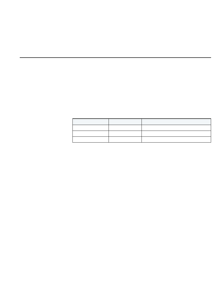
JTAG Support
69
MOTOROLA GENERAL BUSINESS INFORMATION
C5ENPA1-DS/D REV 03
JTAG Support
The C-5e NP contains JTAG test logic compliant with the IEEE 1149.1 specification. All
required public instructions are implemented, as well as some optional instructions. This
section contains information regarding the pinout, instructions, identification codes, and
boundary scan cell types.
Pinout
The C-5e NP uses the standard JTAG pins including the optional test reset pin.
Table 30
describes the pins and their functions.
JTAG Data Registers
The C-5e NP contains the standard internal registers as specified in IEEE 1149.1. These
registers are described in
Table 33
.
Boundary Scan Restriction
SCLK/SCLKX inputs must not toggle when exercising the boundary scan function for JTAG.
Boundary Scan Cell Types
The C-5e NP boundary scan register contains only two cell types. All input cells are observe
only cells of type BC_4. All enable and output cells are standard cells of type BC_1. In IEEE
1149.1-1990 specification, the BC_4 cell is shown in
Figure 7
and the BC_1 cell is shown in
Figure 8
.
Table 33 JTAG Internal Register Descriptions
REGISTER NAME
REGISTER LENGTH
DESCRIPTION
Bypass
1
Standard JTAG bypass register
Boundary
1549
Boundary Scan Register
Device Identification
32
Standard JTAG IDCODE Register

70
CHAPTER 2: SIGNAL DESCRIPTIONS
C5ENPA1-DS/D REV 03
MOTOROLA GENERAL BUSINESS INFORMATION
Figure 7 Observe-Only Cell
Figure 8 Cell Design That Can Be Used for Both Input and Output Pins
G1
0
1
1D
C1
From System Pin
To next cell
To System Logic
Shift
DR
F
r
om la
st cell
Cl
o
c
k DR
G1
0
1
1D
C1
To/From
System Pin
To next cell
From/To
System
Shift DR
From last cell
Clock DR
1D
C1
G1
0
1
Update DR
Node
JTAG Support
71
MOTOROLA GENERAL BUSINESS INFORMATION
C5ENPA1-DS/D REV 03
IDcode Register
The C-5e NP implements a standard 32bit JTAG identification register.
Table 34
lists the
value of the code for full identification and its subcomponents.
The concatenated 32bit value is hexidecimal 0002132d.
JTAG Instruction Register
The C-5e NP contains a 4bit instruction register.
Table 35
lists the instructions that are
supported.
Table 34 JTAG Identification Code and Its Subcomponents
FIELD NAME
WIDTH
BIT POSITIONS
BINARY VALUE
Version
4
31-28
0000
Part Number
16
27-12
0000_0000_0010_0001
Manufacturer Identity
11
11-1
001_1001_0110
LSB
1
0
1
Table 35 Instruction Register Instructions
INSTRUCTION MNEMONIC SELECTED REGISTER
INSTRUCTION OPCODE
Extest
Boundary Scan
0000
Idcode
Identification Register
0001
Sample/Preload
Boundary Scan
0010
Highz
Bypass Register
0011
Clamp
Bypass Register
0100
Bypass
Bypass Register
0101
Reserved*
Bypass Register
0110
Reserved*
Bypass Register
0111
Bypass
Bypass Register
1000
Bypass
Bypass Register
1001
Bypass
Bypass Register
1010
Bypass
Bypass Register
1011
Bypass
Bypass Register
1100
Bypass
Bypass Register
1101
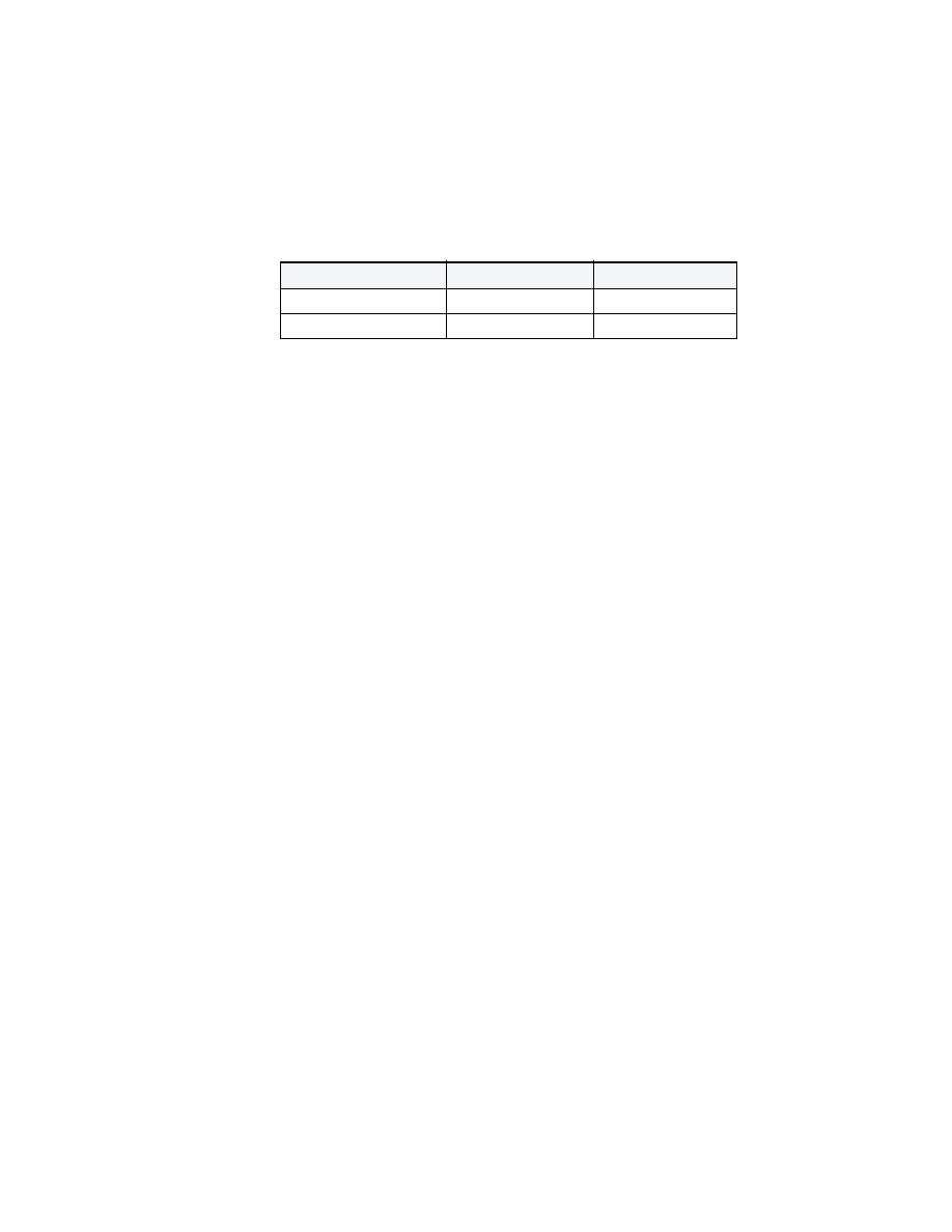
72
CHAPTER 2: SIGNAL DESCRIPTIONS
C5ENPA1-DS/D REV 03
MOTOROLA GENERAL BUSINESS INFORMATION
Boundary Scan
Description Language
In order to simplify board test, Motorola Corporation has provided a boundary scan
description language (BSDL) file (c5e.bsdl) in the Motorola web site that describes the
complete set of instructions, boundary scan order, and identification code value in an
industry standard format.
http://www.motorola.com/networkprocessors
Bypass
Bypass Register
1110
Bypass
Bypass Register
1111
*
There are two reserved instructions intended for Motorola Corporation's internal
use. These should not be programmed by users.
Table 35 Instruction Register Instructions (continued)
INSTRUCTION MNEMONIC SELECTED REGISTER
INSTRUCTION OPCODE

MOTOROLA GENERAL BUSINESS INFORMATION
C5ENPA1-DS/D REV 03
C5ENPA1-DS/D
Rev 03
Chapter 3
ELECTRICAL SPECIFICATIONS
Absolute Maximum
Ratings
Table 36
lists the absolute maximum ratings for the C-5e network processor. Stresses
beyond those listed may cause permanent damage to the device. These are stress ratings
only and do not imply that operation under any conditions other than those listed under
"
Recommended Operating Conditions
" (
Table 37
) is possible.
Exposure to conditions beyond
Table 36
can:
�
Reduce device reliability
�
Result in premature device failure, even with no immediate sign of failure
Prolonged exposure to conditions at or near the absolute maximum ratings could also
result in reduced useful life and reliability of the C-5e NP.
Table 36 C-5e Network Processor Absolute Maximum Ratings
PARAMETER
MIN
MAX
UNIT
V
DD33/VDDT/VDDF
Supply Voltage (3.3V input)*
*
Voltages are relative to Ground
-0.5
+5
V
V
DD
Supply Voltage (1.2V input)*
-0.5
+2.2
V
Voltage on any pin
-0.5
V
DD33
+ 0.5
V
Static Discharge Voltage
2000/500
V
Storage Temperature
-40
+125
�C
Absolute Maximum Junction Temperature
-40
+125
�C
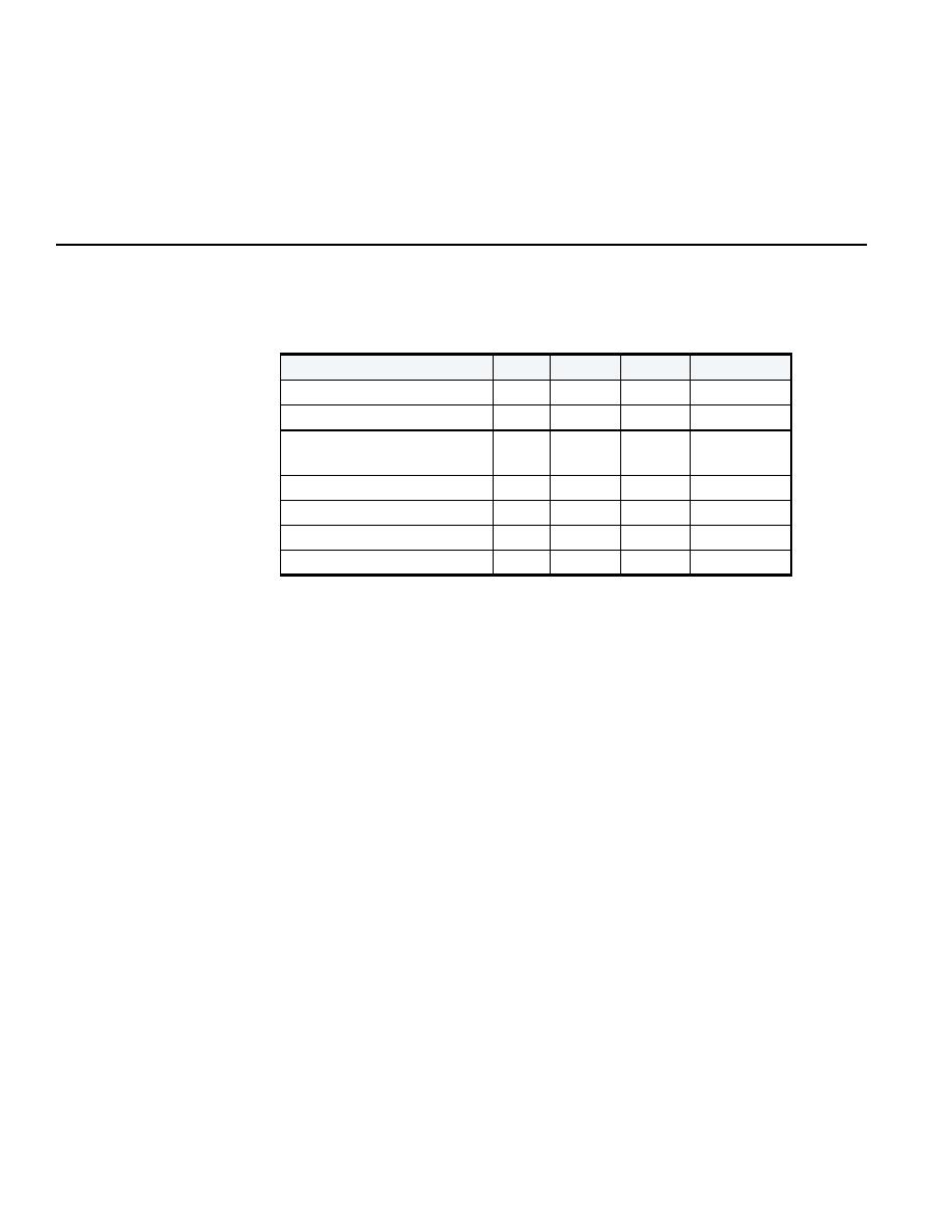
74
CHAPTER 3: ELECTRICAL SPECIFICATIONS
C5ENPA1-DS/D REV 03
MOTOROLA GENERAL BUSINESS INFORMATION
Recommended Operating
Conditions
The recommended operating conditions describe an environment the C-5e NP network
processor is expected to encounter during normal operation.
Table 37
delineates the
recommended operating parameters for the C-5e NP.
Table 37 C-5e Network Processor
Recommended Operating Conditions
PARAMETER
MIN
NOMINAL MAX
UNIT
V
DD33
Supply Voltage
3.135
3.3
3.465
V
V
DDT
Supply Voltage
3.135
3.3
3.465
V
V
DDF
Supply Voltage
2.375
3.135
2.5
3.3
2.625*
3.465
*
For FP operation with I/Os @ 2.5V nominal.
For FP operation with I/Os @ 3.3V nominal.
V
V
DD
Supply Voltage
1.14
1.2
1.26
V
I
DD33
- V
DD33
Supply Current
1.3
A
I
DD
- V
DD
Supply Current
8.5
A
T
j
Junction Temperature
-40
125
�C

DC Characteristics
75
MOTOROLA GENERAL BUSINESS INFORMATION
C5ENPA1-DS/D REV 03
DC Characteristics
The DC electrical characteristics define the input operating conditions for proper
operation and the output responses to applied DC signals and switch characteristics over
specified voltage and temperature ranges. The DC electrical characteristics are specified
within the recommended operating conditions including operating temperature and power
supply range as stated in this data sheet.
Table 38
outlines the C-5e NP DC characteristics.
Each control input pin has a capacitance associated with it. The capacitance at the control
input is due to the package and the input circuitry connected to the pin. Capacitance is
based on these conditions: T
A
= 25
�C
; V
DD33
= 3.3V; f = 1MHz.
Table 39
provides
capacitance data.
Table 38 C-5e Network Processor DC Characteristics
PARAMETER*
*
All voltages are relative to Ground unless otherwise indicated.
MIN
MAX
UNIT
NOTES
LVTTL
Input High Voltage
2.0
V
DD33
+.3
V
LVTTL Input Low Voltage
-0.3
0.8
V
LVTTL
Output High Voltage
2.4
V
@I
OH
= -2mA
LVTTL Output Low Voltage
0.4
V
@I
OL
= +2mA
LVTTL Input Current
-100
+100
�
A
V
IN
= 0V or V
DD33
LVPECL
Input High Voltage
V
DD33
-1.165
V
DD33
+.3V
V
LVPECL Input Low Voltage
-0.3
V
DD33
-1.475
V
LVPECL
Output High Voltage
V
DD33
-1.025
V
DD33
-0.60
V
Load = 50ohm to
V
DD33
- 2V
LVPECL Output Low Voltage
V
DD33
-2.20
V
DD33
-1.620
V
Load = 50ohm to
V
DD33
- 2V
LVPECL Input Current
-100
+100
�
A
CPREF
V
DD33
-1.38
V
DD33
-1.26
V
Single-ended LVPECL
reference
Table 39 C-5e Network Processor Capacitance Data
PARAMETER
TYPICAL
UNIT
All Pins
5
pF
76
CHAPTER 3: ELECTRICAL SPECIFICATIONS
C5ENPA1-DS/D REV 03
MOTOROLA GENERAL BUSINESS INFORMATION
Power Sequencing
It is intended that the VDD33/VDDT/VDDF and VDD rails are sequenced to their final value
together for most applications. VDD33, VDDT and VDDF must be above VDD at all times.
VDD must be brought to its final value within 100ms of sequencing on VDD33, VDDT and
VDDF.
It is also required that SCLK, SCLKX, TCLKI, PCLK, MDCLK, FTXCLK, and FRXCLK be running
or begin running during power sequencing to propagate reset inside the C-5e NP.
Figure 9
indicates the relationship between the clocks and PRSTX. There is no requirement that the
asserting and deasserting edges of PRSTX be synchronous to the clocks. Reset must be
asserted within 100
�
s of power initiation. Typically, reset is held low during power
initiation.
Figure 9 Bringup Clock Timing Diagram
TCLKI, PCLK,
SCLK, SCLKX,
MDCLK, FTXCLK,
FRXCLK
PRSTX
�
1ms
�
100
�
s
(
(
)
)
100
�
s
VDD, VDD33,
VDDT, VDDF

Power and Thermal Characteristics
77
MOTOROLA GENERAL BUSINESS INFORMATION
C5ENPA1-DS/D REV 03
Power and Thermal
Characteristics
Table 40
provides the derived power and thermal characteristics for the production
version of the C-5e NP.
Table 40
note: Power dissipation values assume the following conditions:
�
BMU memory operating at 133MHz.
�
TLU memory operating at 133MHz.
�
QMU operating at 175MHz.
�
VDD = 1.2V, VDD33 = 3.3V, TJ at approximately 50�C for typical values. VDD and VDD33
are 5% higher for maximum values.
�
"Minimum" PD based on idle condition (clocks running and no programs executing).
�
"Typical" PD based on test application that implements Fast Ethernet forwarding
actively running on all CPs.
�
"Maximum" PD based on maximum consumption for any high-bandwidth
communications application executing on all CPs, FP, and XP.
Thermal Management
Information
This section provides thermal management information for the ceramic ball grid array
(CBGA) package for air-cooled applications. Proper thermal control design is primarily
dependent on the system-level design--the heat sink, airflow, and thermal interface
material. To reduce the die-junction temperature, heat sinks may be attached to the
package by several methods--spring clip to holes in the printed-circuit board or package,
and mounting clip and screw assembly (refer to
Figure 10
); however, due to the potential
Table 40 C-5e Network Processor Power and Thermal Characteristics
PARAMETER
MIN
TYP
MAX
UNITS
TEST CONDITIONS
Power Dissipation, P
D
5.5
9.2
13.0
W
266MHz core clock
See Note below
Maximum Junction
Temperature, T
J
125
o
C
See Note below
Thermal Resistance, junction
to case,
JC
<0.1
o
C/W
See Note below
Thermal Resistance, junction
to printed circuit board,
JB
4.8
o
C/W
See Note below
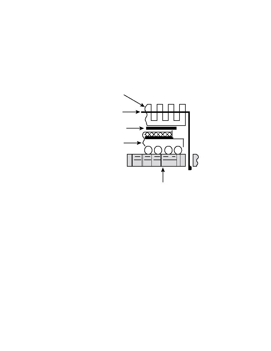
78
CHAPTER 3: ELECTRICAL SPECIFICATIONS
C5ENPA1-DS/D REV 03
MOTOROLA GENERAL BUSINESS INFORMATION
large mass of the heat sink, attachment through the printed circuit board is suggested. If a
spring clip is used, the spring force should not exceed 5.5 pounds.
Figure 10 Package Cross Section View with Several Heat Sink Options
Internal Package Conduction Resistance
For the exposed-die packaging technology the intrinsic conduction thermal resistance
paths are as follows:
�
The die junction-to-case (or top-of-die for exposed silicon) thermal resistance
�
The die junction-to-ball thermal resistance
Figure 11
depicts the primary heat transfer path for a package with an attached heat sink
mounted to a printed-circuit board.
CBGA Package
Heat Sink
Heat Sink Clip
Thermal Interface Material
Printed Circuit Board
Power and Thermal Characteristics
79
MOTOROLA GENERAL BUSINESS INFORMATION
C5ENPA1-DS/D REV 03
Figure 11 Package with Heat Sink Mounted to the Printed Circuit Board
Heat generated on the active side of the chip is conducted through the silicon, then
through the heat sink attach material (or thermal interface material), and finally to the
heat sink where it is removed by convection.
Because the silicon thermal resistance is quite small, for a first-order analysis, the
temperature drop in the silicon may be neglected. Thus, the thermal interface material
and the heat sink conduction/convective thermal resistances are the dominant terms.
Heat Sink Selection Example
For preliminary heat sink sizing, the die-junction temperature can be expressed as follows:
T
j
= T
a
+ T
r
+ (
jc
+
int
+
sa
) x P
d
where:
T
j
is the die-junction temperature
T
a
is the inlet cabinet ambient temperature
T
r
is the air temperature rise within the computer cabinet
External Resistance
Internal Resistance
External Resistance
Radiation
Heat Sink
Printed Circuit Board (PCB)
Radiation
Convection
Thermal Interface Material
Die/Package
Die Junction
Package/Leads
Convection

80
CHAPTER 3: ELECTRICAL SPECIFICATIONS
C5ENPA1-DS/D REV 03
MOTOROLA GENERAL BUSINESS INFORMATION
jc
is the junction-to-case thermal resistance
int
is the adhesive or interface material thermal resistance
sa
is the heat sink base-to-ambient thermal resistance
P
d
is the power dissipated by the device
During operation, the die-junction temperatures (T
j
) should be maintained less than the
value specified in
Table 40
. The temperature of the air cooling the component greatly
depends upon the ambient inlet air temperature and the air temperature rise within the
electronic cabinet. An electronic cabinet inlet-air temperature (T
a
) may range from 30� to
40�C. The air temperature rise within a cabinet (T r ) may be in the range of 5� to 10�C. The
thermal resistance of the thermal interface material (
int
) is typically about 1.5�C/W. For
example, assuming a T
a
of 30�C, a T
r
of 5�C, a CBGA package
jc
= 0.1, and a maximum
power consumption (P
d
) of 13.0 W, the following expression for T
j
is obtained:
Die-junction temperature: T
j
= 30�C + 5�C + (0.1�C/W + 1.5�C/W +
sa
) x 13.0 W
For this example, a
sa
value of 5.3�C/W or less is required to maintain the die junction
temperature below the maximum value of
Table 40
.
Though the die junction-to-ambient and the heat sink-to-ambient thermal resistances are
a common figure-of-merit used for comparing the thermal performance of various
microelectronic packaging technologies, one should exercise caution when only using
this metric in determining thermal management because no single parameter can
adequately describe three-dimensional heat flow. The final die-junction operating
temperature is not only a function of the component-level thermal resistance, but the
system-level design and its operating conditions. In addition to the component's power
consumption, a number of factors affect the final operating die-junction
temperature--airflow, board population (local heat flux of adjacent components), heat
sink efficiency, heat sink attach, heat sink placement, next-level interconnect technology,
system air temperature rise, altitude, etc.
Due to the complexity and the many variations of system-level boundary conditions for
today's microelectronic equipment, the combined effects of the heat transfer
mechanisms (radiation, convection,and conduction) may vary widely. For these reasons,
we recommend using conjugate heat transfer models for the board, as well as
system-level designs.
AC Timing Specifications
81
MOTOROLA GENERAL BUSINESS INFORMATION
C5ENPA1-DS/D REV 03
AC Timing Specifications
AC timing specifications consist of input requirements and output responses. The input
requirements include setup and hold times, pulse widths, and high and low times. The
output responses include delays from clock to signal. The AC timing specifications are
defined separately for each interface to the C-5e NP.
See
Figure 12
. Output timing specifications for LVTTL pins are given with a 20pF load on
the output. Other loads can be simulated with the IBIS model available from Motorola.
The LVPECL driver is specified into a 50
load terminated to a (VDD33 - 2V) reference.
Figure 12 Test Loading Conditions
+
2V
LVTTL
LVPECL
DUT
DUT
20pF
50
VDD33
82
CHAPTER 3: ELECTRICAL SPECIFICATIONS
C5ENPA1-DS/D REV 03
MOTOROLA GENERAL BUSINESS INFORMATION
Clock Timing
Specifications
The system clock timing is shown in
Figure 13
and described in
Table 41
.
Figure 13 System Clock Timing Diagram
T
sc
T
sh
SCLK
Cycle 1
Cycle 2
Cycle 3
Cycle 4
Cycle 5
SCLKX
CCLKn
T
ccN
T
sl
T
cch
T
ccl
Table 41 System Clock Timing Description
SYMBOL PARAMETER
MIN
TYP
MAX
UNIT
COMMENT
Tsc
System Cycle Time 3.76
ns
266MHz core clock
Tsh
Sys Clk High Pulse
45
55
Duty cycle*
*
Pulse duty cycle measured at crossing voltage of SCLK/SCLKX
Tsl
Sys Clk Low Pulse
45
55
Duty cycle*
Tcc0
CCLK0 Cycle Time
647.67
ns
T1
Tcc1
CCLK1 Cycle Time
488.28
ns
E1
Tcc2
CCLK2 Cycle Time
29.097
ns
E3
Tcc3
CCLK3 Cycle Time
22.353
ns
T3
Tcc4
CCLK4 Cycle Time
20.00
ns
RMII
Tcc5
CCLK5 Cycle Time
9.412
ns
Fibre Channel
Tcc6
CCLK6 Cycle Time
8.00
ns
GMII
Tcc7
CCLK7 Cycle Time
6.43
ns
OC-3
Tcch
CCLKm High Time
40%
60%
% cycle pulse is high
Tccl
CCLKm Low Time
40%
60%
% cycle pulse is low
AC Timing Specifications
83
MOTOROLA GENERAL BUSINESS INFORMATION
C5ENPA1-DS/D REV 03
CP Timing Specifications
This section describes the timing for the following CP interfaces:
�
DS1/DS3
�
10/100 Ethernet
�
Gigabit Ethernet
�
OC-3
�
OC-12
DS1/DS3 Timing Specifications
The DS1/DS3 interface timing is shown in
Figure 14
and described in
Table 42
.
Figure 14 DS1/DS3 Ethernet Timing Diagram
The frequencies specified for CCLK0 - CCLK7 allow full flexibility for the C-5e NP. It is also possible to use one
or more CCLKn inputs for other frequencies; contact your Motorola representative for more information.
CPn_0 (TCLK)
Cycle 1
Cycle 2
Cycle 2
Cycle 3
Cycle 3
Cycle 4
Cycle 4
Cycle 5
Cycle 5
CPn_2/3 (Tx)
CPn_1 (RCLK)
CPn_4/5 (Rx)
T
cdt
T
cdo
T
cdr
T
cds
T
cdh
84
CHAPTER 3: ELECTRICAL SPECIFICATIONS
C5ENPA1-DS/D REV 03
MOTOROLA GENERAL BUSINESS INFORMATION
10/100 Ethernet Timing Specifications
The 10/100 Ethernet interface timing is shown in
Figure 15
and described in
Table 43
.
Figure 15 10/100 Ethernet Timing Diagram
Table 42 DS1/DS3 Ethernet Timing Description
SYMBOL
PARAMETER
MIN
TYP
MAX
UNIT
Tcdt
DS1/DS3 Transmit Cycle Time
647/22.4
ns
Tcdo
DS1/DS3 Output Time
3.0/3.0
400/15.0
ns
Tcdr
DS1/DS3 Receive Cycle Time
647/22.4
ns
Tcds
DS1/DS3 Setup Time
2.0
ns
Tcdh
DS1/DS3 Hold Time
0
ns
CPn_0 (TCLK)
Cycle 1
Cycle 2
Cycle 3
Cycle 4
Cycle 5
CPn_2/3/6 (Tx)
CPn_1/4/5 (Rx)
T
cet
T
ceo
T
ces
T
ceh
Table 43 10/100 Ethernet Timing Description
SYMBOL
PARAMETER
MIN
TYP
MAX
UNIT
Tcet
Transmit Cycle Time*
*
STD/Fast Ethernet
20
ns
Tceo
Output Time
3.0
15.0
ns
Tces
Setup Time
2.0
ns
Tceh
Hold Time
0
ns
AC Timing Specifications
85
MOTOROLA GENERAL BUSINESS INFORMATION
C5ENPA1-DS/D REV 03
Gigabit GMII Ethernet, TBI and MII Interface Timing Specifications
The Gigabit GMII Ethernet interface timing is shown in
Figure 16
and described in
Table 44
. The TBI interface timing is shown in
Figure 16
and described in
Table 45
.
Figure 16 Gigabit Ethernet and TBI Interface Timing Diagram
Cycle 1
Cycle 2
Cycle 3
T
cmt
T
cmo
MII Tx
Cycle 1
Cycle 2
Cycle 3
Cycle 4
Cycle 5
T
cgt
T
cgo
GMII / TBI Tx
Cycle 1
Cycle 2
Cycle 3
Cycle 4
Cycle 5
T
ctr
T
ctd
T
cts
T
cth
TBI Rx
MII CPn_1 (TCLKI)
MII CPn_2-6 (Tx)
Cycle 1
Cycle 2
Cycle 3
Cycle 4
Cycle 5
CPn+2_1 (RCLK)
T
cgr
T
cgs
T
cgh
GMII/MII Rx
CPn+2_2-6 (Rx)
CPn+3_1-6 (Rx)
CPn_0 (TCLK)
CPn_2-6 (Tx)
CPn+1_2-6 (Tx)
CPn+2_1 (RCLK)
CPn+3_1 (RCLKN)
CPn+2_2-6 (Rx)
CPn+3_2-6 (Rx)

86
CHAPTER 3: ELECTRICAL SPECIFICATIONS
C5ENPA1-DS/D REV 03
MOTOROLA GENERAL BUSINESS INFORMATION
Table 44 Gigabit GMII/MII Ethernet Interface Timing Description
SYMBOL
GIGABIT
PARAMETER
MIN
TYP
MAX
UNIT
COMMENT
Tcgt
Transmit Cycle Time, GMII
8.0
ns
Tcgo
Output Time, GMII
3.0
6.0
ns
Tcgr
Receive Cycle Time
8.0
ns
Tcgs
Setup Time
2.0
ns
Tcgh
Hold Time
0.0
ns
Tcmt
Transmit Cycle Time, MII
40/400
ns
100BaseT/10BaseT
Tcmo
Output Time, MII
2
8
ns
Table 45 Gigabit TBI Interface Timing Description
SYMBOL
TBI
PARAMETER
MIN
TYP
MAX
TOL
UNIT
Tctt
Transmit Cycle Time
8.0
ns
Tcto
Output Time
3.0
6.0*
*
For Fibre Channel applications this value is 7.0ns for a transmit cycle time of 9.4ns.
ns
Tctr
Receive Cycle Time
16.0
ns
Tctd
Rclk/Rclkn Deviation
1.0
ns
Tcts
Setup Time
2.0
ns
Tcth
Hold Time
0.0
ns
AC Timing Specifications
87
MOTOROLA GENERAL BUSINESS INFORMATION
C5ENPA1-DS/D REV 03
OC-3 Timing Specifications
The OC-3 interface timing is shown in
Figure 17
and described in
Table 46
.
Figure 17 OC-3 Timing Diagram
Cycle 1
Cycle 2
Cycle 3
Cycle 4
Cycle 5
CPn_2
Cycle 1
Cycle 2
Cycle 3
Cycle 4
Cycle 5
CPn_3
CPn_0
CPn_1
CPn_4
CPn_5
T
c3t
T
c3r
T
c3d
T
c3i
T
c3s
T
c3h
T
c3s
T
c3h
Table 46 OC-3 Timing Description
SYMBOL
PARAMETER
MIN
TYP
MAX
UNIT
Tc3t
OC-3 Transmit Cycle Time
6.43
ns
Tc3i
OC-3 Pulse Width
2.0
ns
Tc3r
OC-3 Receive Cycle Time*
*
155.52MHz
6.0
ns
Tc3d
OC-3 Clock Duty Cycle
40
60
%
Tc3s
OC-3 Setup Time
2.0
ns
Tc3h
OC-3 Hold Time
0.0
ns
88
CHAPTER 3: ELECTRICAL SPECIFICATIONS
C5ENPA1-DS/D REV 03
MOTOROLA GENERAL BUSINESS INFORMATION
OC-12 Timing Specifications
The OC-12 interface timing is shown in
Figure 18
and described in
Table 47
.
Figure 18 OC-12 Timing Diagram
CPn_1 (TCLKI)
Cycle 1
Cycle 1
Cycle 2
Cycle 3
Cycle 3
Cycle 4
Cycle 5
CPn_0 (TCLK)
CPn+1_2-5 (Tx)
CPn_1 (RCLK)
CPn+2_2-6 (Rx)
CPn+3_2-5 (Rx)
T
c12i
T
c12t
T
c12r
T
c12o
T
c12s
T
c12h
Cycle 2
T
c12d
Table 47 OC-12 Timing Description
SYMBOL
PARAMETER
MIN
TYP
MAX
UNIT
Tc12i
OC-12 Transmit Cycle Time*
*
Input from PHY
12.86
ns
Tc12d
OC-3 Clock Duty Cycle
40
60
%
Tc12t
OC-12 Transmit Cycle Time
Output from C-5e NP
12.86
ns
Tc12o
OC-12 Output Time
Aligned to TCLK
3.0
10.0
ns
Tc12r
OC-12 Receive Cycle Time
12.0
12.86
ns
Tc12s
OC-12 Setup Time
2.0
ns
Tc12h
OC-12 Hold Time
0.0
ns
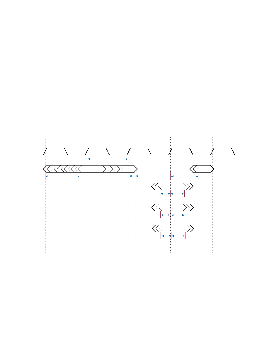
AC Timing Specifications
89
MOTOROLA GENERAL BUSINESS INFORMATION
C5ENPA1-DS/D REV 03
Executive Processor
Timing Specifications
The XP timing specifications include:
�
PCI Timing Specifications
�
MDIO Serial Interface Timing Specifications
�
Low Speed Serial Interface Timing Specifications
�
PROM Interface Timing Specifications
PCI Timing Specifications
The PCI timing is shown in
Figure 19
and described in
Table 48
.
Figure 19 PCI Timing Diagram
PCLK
Cycle 1
Cycle 2
Cycle 3
Cycle 4
Cycle 5
PAD/P_ctl
(output)
PAD/P_ctl
(input)
PGNTX
(input)
PIDSEL
(input)
T
pc
T
pao
T
pav
T
paz
T
pas
T
pah
T
pgs
T
pgh
T
pis
T
pih

90
CHAPTER 3: ELECTRICAL SPECIFICATIONS
C5ENPA1-DS/D REV 03
MOTOROLA GENERAL BUSINESS INFORMATION
Table 48 PCI Timing Description
SYMBOL
PARAMETER
MIN
TYP
MAX
UNIT
Tpc
PCI Cycle Time*
*
66MHz PCI
15.0
ns
Tpas
PAD/P_ctl Setup
P_ctl includes all PCI control parameters including: PPAR, PFRAMEX, PTRDYX, PIRDYX,
PSTOPX, PDEVSELX, PPERRX, PSERRX
3.0
ns
Tpah
PAD/P_ctl Hold
0.0
ns
Tpao
PAD/P_ctl Output
2.0
6.0
ns
Tpaz
PAD/P_ctl Clk to Tri
Not fully tested, values based on design/characterization.
2.0
6.0
ns
Tpav
PAD/P_ctl Clk to Driven
2.0
6.0
ns
Tpgs
PGNTX Setup
5.1
ns
Tpgh
PGNTX Hold
0.0
ns
Tpis
PIDSEL Setup
3.0
ns
Tpih
PIDSEL Hold
0.0
ns
PRSTX**
**
Asynchronous
ns
PINTA**
ns
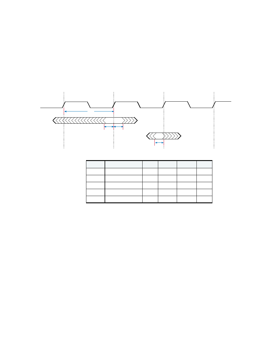
AC Timing Specifications
91
MOTOROLA GENERAL BUSINESS INFORMATION
C5ENPA1-DS/D REV 03
MDIO Serial Interface Timing Specifications
The MDIO serial interface timing is shown in
Figure 20
and described in
Table 49
.
Figure 20 MDIO Serial Interface Timing Diagram
Cycle 2
Cycle 3
Cycle 4
T
sic
T
sids
SICL
SIDA
(output)
SIDA
(input)
T
sods
T
sodh
Table 49 MDIO Serial Interface Timing Description
SYMBOL
PARAMETER
MIN
TYP
MAX
UNIT
Tsic
SICL Cycle Time
40
ns
Tsids
SIDA Input Setup
10
ns
Tsidh
SIDA Input Hold
0.0
ns
Tsods
SIDA Output Setup
10
ns
Tsodh
SIDA Output Hold
10
ns
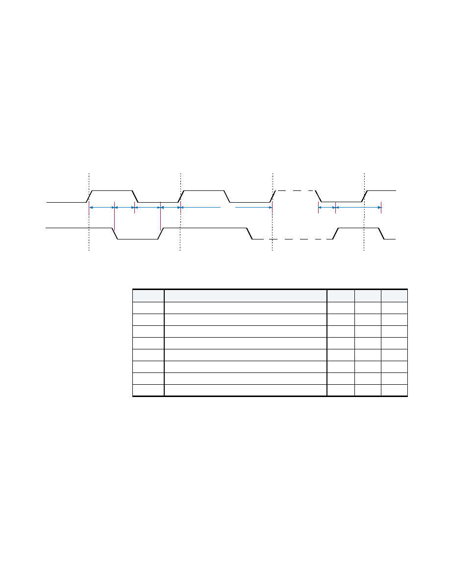
92
CHAPTER 3: ELECTRICAL SPECIFICATIONS
C5ENPA1-DS/D REV 03
MOTOROLA GENERAL BUSINESS INFORMATION
Low Speed Serial Interface Timing Specifications
The low speed serial interface timing is shown in
Figure 21
and described in
Table 50
.
Figure 21 Low Speed Serial Interface Timing Diagram
Cycle 2
Cycle 3
T
slc
T
slss
T
slhd
T
slsd
T
slhs
SICL
SIDA
T
slst
T
slb
Table 50 Low Speed Serial Interface Timing Description
SYMBOL
PARAMETER
MIN
MAX
UNIT
Tslc
SICL Cycle Time
2500
ns
Tslss
Set-up Time for Repeated START Condition
600
ns
Tslhs
Hold Time START Condition
600
ns
Tslsd
Data Set-up Time
250
ns
Tslhd
Data Hold Time
0.0
ns
Tslst
Set-up Time for STOP Condition
600
ns
Tslb
Bus Free Time Between a STOP and START Condition
1250
ns
Cmax
Capacitive load for each line of the bus
400
pF

AC Timing Specifications
93
MOTOROLA GENERAL BUSINESS INFORMATION
C5ENPA1-DS/D REV 03
PROM Interface Timing Specifications
The PROM interface timing is shown in
Figure 22
and described in
Table 51
.
Figure 22 PROM Interface Timing Diagram
SPCK
Cycle 1
Cycle 2
Cycle 3
Cycle 4
Cycle 5
SPDI
SPLD
SPDO
T
spc
T
splo
T
spis
T
spih
T
spdo
Table 51 PROM Interface Timing Description
SYMBOL
PARAMETER
MIN
TYP
MAX
UNIT
Tspc
SPCK Cycle Time
40.0
ns
Tspis
SPDI Setup
10.0
ns
Tspih
SPDI Hold
0.0
ns
Tsplo
SPLD Output
Tsc
Tsc + 3.0
ns
Tspdo
SPDO Output
Tsc
Tsc + 3.0
ns
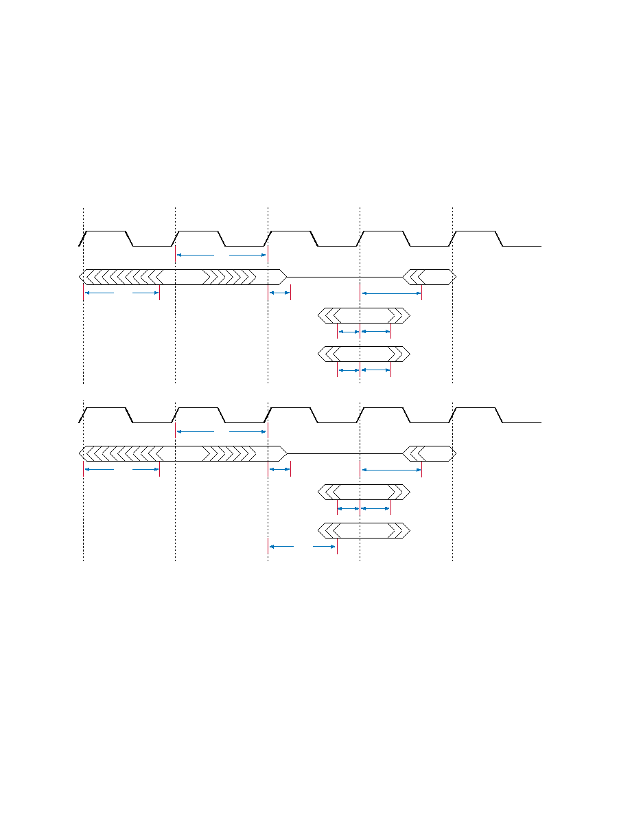
94
CHAPTER 3: ELECTRICAL SPECIFICATIONS
C5ENPA1-DS/D REV 03
MOTOROLA GENERAL BUSINESS INFORMATION
Fabric Processor Timing
Specifications
The FP timing specifications are shown in
Figure 23
and described in
Table 52
.
Figure 23 Fabric Processor Timing Diagram
FRXCLK
Cycle 1
Cycle 2
Cycle 3
Cycle 4
Cycle 5
FRXCTL
(output)
FRXCTL
(input)
FINn
T
frc
T
frco
T
frcv
T
frcz
T
frcs
T
frch
T
frds
T
frdh
T
ftcs
T
ftch
FTXCLK
FTXCTL
(output)
FTXCTL
(input)
FOUTn
T
ftc
T
ftco
T
ftcv
T
ftcz
T
ftdo

AC Timing Specifications
95
MOTOROLA GENERAL BUSINESS INFORMATION
C5ENPA1-DS/D REV 03
Table 52 Fabric Processor Timing Description
SYMBOL
PARAMETER
MIN
TYP
MAX
UNIT
COMMENT
Tfrc
FRX Cycle Time
8.0
ns
Tfrcs
FRXCTL Setup
4.0
1.5
ns
Utopia2 Mode
All other modes
Tfrch
FRXCTL Hold
0.0
ns
Tfrco
FRXCTL Output
1.0
4.0
ns
Tfrcz
FRXCTL Clk to Tri*
*
Not fully tested, values based on design/characterization.
1.0
4.0
ns
Tfrcv
FRXCTL Clk to Driven*
1.0
4.0
ns
Tfrds
FIN Setup
4.0
1.5
ns
Utopia2 Mode
All other modes
Tfrdh
FIN Hold
0.0
ns
Tftc
FTX Cycle Time
8.0
ns
Tftcs
FTXCTL Setup
4.0
1.5
ns
Utopia2 Mode
All other modes
Tftch
FTXCTL Hold
0.0
ns
Tftco
FTXCTL Output
1.0
4.0
ns
Tftcz
FTXCTL Clk to Tri*
1.0
4.0
ns
Tftcv
FTXCTL Tri to Driven*
1.0
4.0
ns
Tftdo
FOUT Output
1.0
4.0
ns
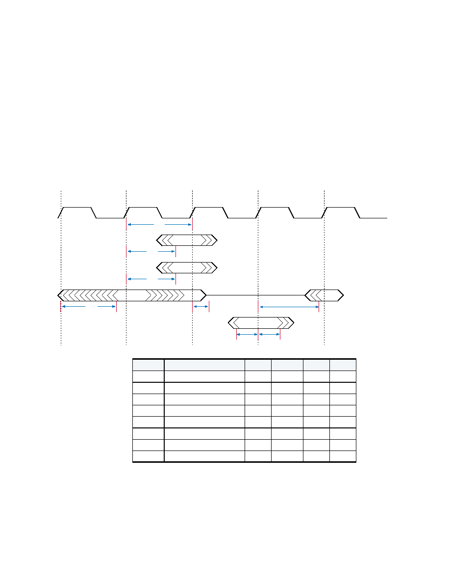
96
CHAPTER 3: ELECTRICAL SPECIFICATIONS
C5ENPA1-DS/D REV 03
MOTOROLA GENERAL BUSINESS INFORMATION
BMU Timing
Specifications
The BMU timing specifications are shown in
Figure 24
and described in
Table 53
.
The BMU synchronous DRAM interface is PC100-compliant and designed to work with
industry standard SDRAM components with 12 or fewer address lines. The information
below is intended to provide the output, setup, and hold data required to design this
interface without duplicating the transaction waveform diagrams in SDRAM data sheets.
Figure 24 BMU Timing Diagram
MDCLK
Cycle 1
Cycle 2
Cycle 3
Cycle 4
Cycle 5
M_ctl
MAn
MDn
(output)
MDn
(input)
T
mc
T
mdo
T
mco
T
mao
T
mdv
T
mds
T
mdz
T
mdh
Table 53 BMU Timing Description
SYMBOL
PARAMETER
MIN
TYP
MAX
UNIT
Tmc
BMU Cycle Time
7.5
ns
Tmco
BMU Ctrl Output
0.8
3.4
ns
Tmao
BMU Addr Output
0.8
3.4
ns
Tmds
BMU Data Setup
0.5
ns
Tmdh
BMU Data Hold
1.1
ns
Tmdo
BMU Data Output
0.8
4.0
ns
Tmdz
BMU Data Clk to Tri*
*
Not fully tested, values based on design/characterization.
0.8
4.0
ns
Tmdv
BMU Data Clk to Driven*
0.8
4.0
ns

AC Timing Specifications
97
MOTOROLA GENERAL BUSINESS INFORMATION
C5ENPA1-DS/D REV 03
Table 54 Signal Groups in BMU Timing Diagrams
SIGNAL GROUP
INCLUDED SIGNALS
Control (M_ctl)
MBA0, MBA1, MCASX, MRASX, MWEX, MCSX, MDQM, MDQML
Address (MAn)
MA0 - MA11
Data (MDn)
MD0 - MD129, MDECC0 - MDECC8
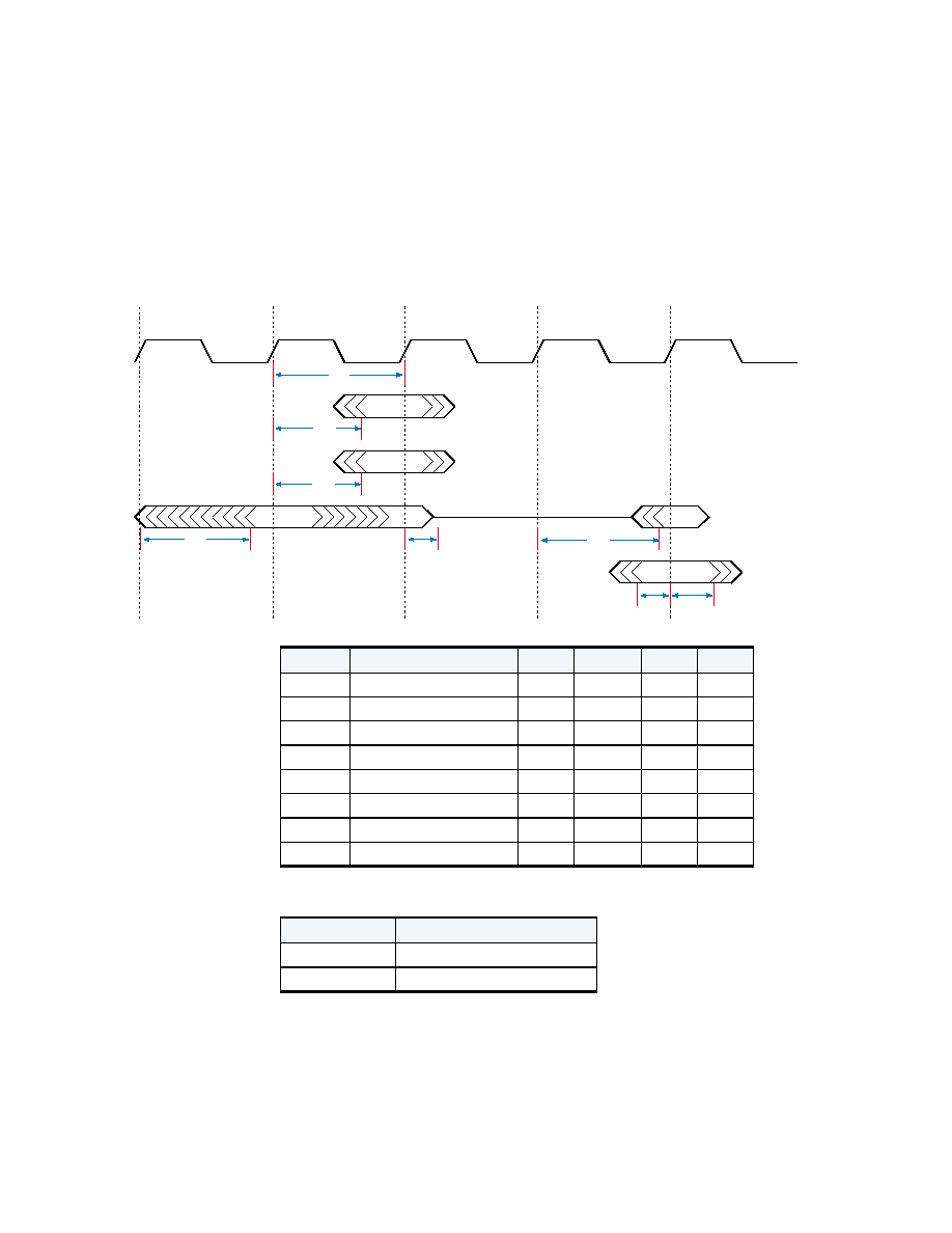
98
CHAPTER 3: ELECTRICAL SPECIFICATIONS
C5ENPA1-DS/D REV 03
MOTOROLA GENERAL BUSINESS INFORMATION
TLU Timing Specifications
The TLU timing specifications are shown in
Figure 25
and described in
Table 55
.
Figure 25 TLU Timing Diagram
TCLKI
Cycle 1
Cycle 2
Cycle 3
Cycle 4
Cycle 5
T_ctl
TAn
TDn
(output)
TDn
(input)
T
tc
T
tdo
T
tco
T
tao
T
tdv
T
tds
T
tdz
T
tdh
Table 55 TLU Timing Description
SYMBOL
PARAMETER
MIN
TYP
MAX
UNIT
Ttc
TLU Cycle Time
7.5
ns
Ttco
TLU Ctrl Output
0.8
3.4
ns
Ttao
TLU Addr Output
0.8
3.4
ns
Ttds
TLU Data Setup
1.0
ns
Ttdh
TLU Data Hold
1.2
ns
Ttdo
TLU Data Output
0.8
3.7
ns
Ttdz
TLU Data Clk to Tri*
*
Not fully tested, values based on design/characterization.
0.8
3.7
ns
Ttdv
TLU Data Clk to Driven*
0.8
3.7
ns
Table 56 Signal Groups in TLU Timing Diagrams
SIGNAL GROUP
INCLUDED SIGNALS
Control (T_ctl)
TCE0X - TCE3X, TWE0X - TWE3X
Address (TAn)
TA0 - TA21

AC Timing Specifications
99
MOTOROLA GENERAL BUSINESS INFORMATION
C5ENPA1-DS/D REV 03
QMU SRAM (Internal
Mode) Timing
Specifications
The QMU SRAM (Internal Mode) timing specifications are shown in
Figure 26
and
described in
Table 57
.
Figure 26 QMU SRAM (Internal Mode) Timing Diagram
Data (TDn)
TD0 - TD63, TPAR0-3
Table 56 Signal Groups in TLU Timing Diagrams
SIGNAL GROUP
INCLUDED SIGNALS
QACLKI
Cycle 1
Cycle 2
Cycle 3
Cycle 4
Cycle 5
Q_ctl
QAn
QDn
(output)
QDn
(input)
T
qc
T
qdo
T
qco
T
qao
T
qdv
T
qds
T
qdz
T
qdh

100
CHAPTER 3: ELECTRICAL SPECIFICATIONS
C5ENPA1-DS/D REV 03
MOTOROLA GENERAL BUSINESS INFORMATION
Table 57 QMU SRAM (Internal Mode) Timing Description
SYMBOL
PARAMETER
MIN
TYP
MAX
UNIT
COMMENT
Tqc
QMU Cycle Time
5.7
ns
Tqco
QMU Ctrl Output
0.8
3.4
ns
Loading is 50
transmission line.
Tqao
QMU Addr Output
0.8
3.4
ns
Loading is 50
transmission line.
Tqds
QMU Data Setup
0.8
ns
Tqdh
QMU Data Hold
0.8
ns
Tqdo
QMU Data Output
0.9
3.4
ns
Loading is 50
transmission line.
Tqdz
QMU Data Clk to Tri*
*
Not fully tested, values based on design/characterization.
0.9
3.4
ns
Tqdv
QMU Data Clk to
Driven*
0.9
3.4
ns
Table 58 Signal Groups in QMU SRAM (Internal Mode) Timing Diagrams
SIGNAL GROUP
INCLUDED SIGNALS
Control (Q_ctl)
QWEX
Address (QAn)
QA0-QA16
Data (QDn)
QD0-QD31, QDPL, QDPH

AC Timing Specifications
101
MOTOROLA GENERAL BUSINESS INFORMATION
C5ENPA1-DS/D REV 03
QMU to Q-5 (External
Mode) Timing
Specifications
The QMU to Q-5 (External Mode) timing specifications are shown in
Figure 27
and
describded in
Table 59
.
Figure 27 QMU to Q-5 (External Mode) Timing Diagram
QACLKI
Cycle 1
Cycle 2
T
qes
QBCLKI
DQDATA
T
qeh
T
qeh
QACLKO
QBCLKO
NQDATA
T
qeomin
T
qeomax
T
qes
T
qep
T
qec
T
qep
T
qec
T
qep
T
qec
T
qep
T
qec
T
qeomin
T
qeomax

102
CHAPTER 3: ELECTRICAL SPECIFICATIONS
C5ENPA1-DS/D REV 03
MOTOROLA GENERAL BUSINESS INFORMATION
Table 59 QMU to Q-5 (External Mode) Timing Description
SYMBOL
PARAMETER
MIN
TYP
MAX
UNIT
COMMENT
Tqec
QMU External Cycle Time
10.0
ns
QACLKO/QBCLKO
derived from
QACLKI/QBCLKI
Tqep
QMU CLKA-CLKB delta
between rising edges
4.8
ns
Tqes
QMU Input Data Setup
0.6
ns
Tqeh
QMU Input Data Hold
0.8
ns
Tqeo
QMU Data Output
-.85
1.3
ns
Determines valid time
for data from each clock
rising edge
Table 60 Signal Groups in QMU to Q-5 (External Mode) Timimg Diagrams
SIGNAL GROUP
INCLUDED SIGNALS
Input Clocks (QnCLKI)
QACLKI, QBCLKI
Output Clocks (QnCLKO)
QACLKO, QBCLKO
Input Data (DQDATA)
QD0-23, QARDY, QDPL, QDPH, QNQRDY, QDQPAR
Output Data (NQDATA)
QA0-16, QWEX, QD24-31
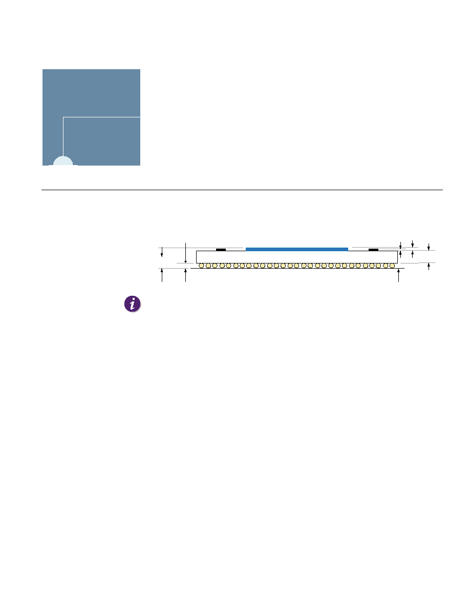
MOTOROLA GENERAL BUSINESS INFORMATION
C5ENPA1-DS/D REV 03
C5ENPA1-DS/D
Rev 03
Chapter 4
MECHANICAL SPECIFICATIONS
Package Views
The C-5e network processor is an 840 pin (29 pins x 29 pins) Ball Grid Array (BGA) package
as shown in the following illustrations.
Table 61
defines the package measurements.
Figure 28 C-5e Network Processor BGA Package Side View
HiTCE: Green ceramic is thermally matched to FR4 circuit board.
A
Seating Plane
A
1
A
2
A
3
A
4
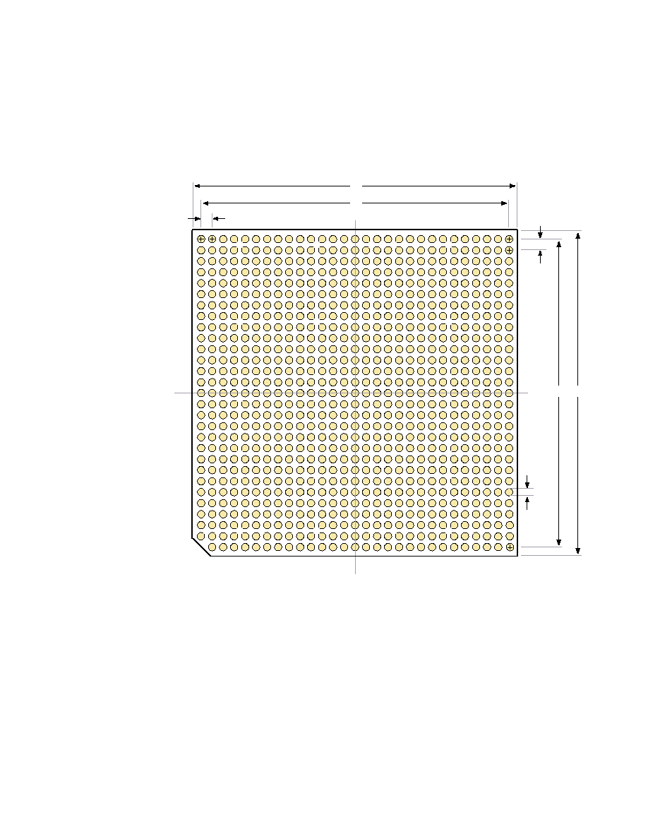
104
CHAPTER 4: MECHANICAL SPECIFICATIONS
C5ENPA1-DS/D REV 03
MOTOROLA GENERAL BUSINESS INFORMATION
Figure 29 C-5e Network Processor BGA Package (Bottom View)
e
b
e
D
E
D
1
E
1
AJ
AH
AG
AF
AE
AD
AC
AB
AA
Y
W
V
U
T
R
P
N
M
L
K
J
H
G
F
E
D
C
B
A
1 2 3 4 5 6 7 8 9 10 11 12 13 14 15 16 17 18 19 20 21 22 23 24 25 26 27 28 29

Package Views
105
MOTOROLA GENERAL BUSINESS INFORMATION
C5ENPA1-DS/D REV 03
Figure 30 C-5e Network Processor BGA Package (Top View)
Probe Pad
Die
18ARS10517D001
Optional
Capacitor
Pads
Optional
Capacitor
Pads
1.65
1.70
0.7
106
CHAPTER 4: MECHANICAL SPECIFICATIONS
C5ENPA1-DS/D REV 03
MOTOROLA GENERAL BUSINESS INFORMATION
Package Measurements
Table 61
defines the C-5e NP package measurements, providing nominal, minimum, and
maximum sizes where appropriate.
At Motorola's discretion up to fourteen (14) capacitors may or may not be attached on
the top of the package.
Marking Codes
Table 62
explains the marking on the C-5e NP.
Table 61 Package Measurements (Reference
Figure 28
,
Figure 29
and
Figure 30
for Symbols)
SYMBOL
DEFINITION
NOM. (MM)
MIN. (MM)
MAX. (MM)
A
Overall
3.26
2.97
3.55
A
1
Ball height
0.70
0.6
0.8
A
2
C4 and Die
0.86
0.82
0.9
A
3
Body thickness
1.7
1.55
1.85
A
4
Capacitor pads
0.6
D
Body size
31.00
30.80
31.20
D
1
Ball footprint (X)
28.00
E
Body size
31.00
30.80
31.20
E
1
Ball footprint (Y)
28.00
e
Ball pitch
1.00
b
Ball diameter
0.70
Table 62 C-5e Network Processor Marking Codes
MARKING (EXPLANATION OF CODES)
Top
Logo/Part#/Date Code
Bottom
N/A
Pin 1 Marking
Chamfered Corner

Reflow
107
MOTOROLA GENERAL BUSINESS INFORMATION
C5ENPA1-DS/D REV 03
Reflow
Typical Reflow Profile for the C-5e Switch Module comprises:
1 Follow the guidelines recommended by your solder paste supplier.
Flux requirements must be met for best solderability.
2 The temperature profile should be carefully characterized to ensure uniform
temperature across the board and package.
Solder ball voiding may be affected by ramp rates and dwell times below and above
liquids.
3 A nitrogen atmosphere is not required, but will make the process more robust. It can
make a difference for marginally solderable PC board pads.
4 Full convection forced air furnaces work best, but IR, Convection/IR, or vapor phase can
be used.

108
CHAPTER 4: MECHANICAL SPECIFICATIONS
C5ENPA1-DS/D REV 03
MOTOROLA GENERAL BUSINESS INFORMATION

MOTOROLA GENERAL BUSINESS INFORMATION
C5ENPA1-DS/D REV 03
C5ENPA1-DS/D
Rev 03
INDEX
Symbols
10/100 Ethernet (RMII) Configuration
34
10/100 Ethernet Signals
34
10/100 Ethernet Timing Description
84
10/100 Ethernet Timing Diagram
84
10/100 Ethernet Timing Specifications
84
A
Absolute Maximum Ratings
73
AC Timing Specifications
81
B
Block Diagram, C-5e Network Processor
20
BMU SDRAM Interface Signals
52
BMU Signal Groups
97
BMU Timing Description
96
BMU Timing Diagram
96
BMU Timing Specifications
96
Boundary Scan Cell Types
69
Boundary Scan Description Language
72
Bringup Clock Timing Diagram
76
Buffer Management Unit
24
C
C-5e Network Processor Absolute Maximum Ratings
73
C-5e Network Processor BGA Package, Bottom View
104
C-5e Network Processor BGA Package, Side View
103
C-5e Network Processor Capacitance Data
75
C-5e Network Processor DC Characteristics
75
C-5e Network Processor Power and Thermal Characteristics
77
C-5e NP Channel Processors
22
Channel Processor Interface Signals
32
Channel Processors
22
Channel Processors Physical Interface Signals and Pins
Grouped by Clusters
33
Clock and Reference Signals
31
Clock Signals
31
Clock Timing Specifications
82
Configuration
10/100 Ethernet (RMII)
34
DS1/T1 Framer Interface
34
FibreChannel TBI
38
Gigabit Ethernet
38
Gigabit Ethernet (GMII)
35
SONET OC-12 Transceiver Interface
40
SONET OC-3 Transceiver Interface
39
Configurations
GMII/TBI Transmit and Receive Pin
36
CP Timing Specifications
83
CSIX-L1 Mode, C-5e Network Processor to Fabric Interface Pin
Mapping
51
D
Data Registers
JTAG
69
DC Characteristics
75
Description
Functional
19
Description Language
Boundary Scan
72
Descriptions
Signal
27
Diagram
10/100 Ethernet Timing
84
BMU Timing
96
Bringup Clock Timing
76
DS1/DS3 Ethernet Timing
83

110
INDEX
C5ENPA1-DS/D REV 03
MOTOROLA GENERAL BUSINESS INFORMATION
Fabric Processor Timing
94
Gigabit Ethernet (TBI) Timing
85
Low Speed Serial Interface Timing
92
MDIO Serial Interface Timing
91
OC-3 Timing
87
PCI Timing
89
Pinout
28
PROM Interface
45
PROM Interface Timing
93
QMU Timing
99
Signal Groups in BMU Timing
97
Signal Groups in QMU Timing
100
Signal Groups in TLU Timing
98
System Clock Timing
82
TLU Timing
98
Diagram, Block
C-5e Network Processor
20
DS1/DS3 Ethernet Timing Description
84
DS1/DS3 Ethernet Timing Diagram
83
DS1/DS3 Timing Specifications
83
DS1/T1 Framer Interface Configuration
34
DS1/T1 Framer Interface Signals
34
E
Electrical Specifications
73
Absolute Maximum Ratings
73
Executive Processor
23
PCI
23
PROM Interface
24
Serial Bus Interface
23
System Interface Signals
42
System Interfaces
23
Executive Processor Timing Specifications
89
F
Fabric Interface Pin Mapping
CSIX-L1 Mode
51
Power X(CSIX-L0) Mode
50
PRIZMA Mode
50
Utopia2/Utopia3 ATM Mode
49
Utopia2/Utopia3 PHY Mode
49
Fabric Processor
24
Fabric Processor Interface Signals
48
Fabric Processor Timing Description
95
Fabric Processor Timing Diagram
94
Fabric Processor Timing Specifications
94
Functional Description
19
G
General System Interface Signal
47
Gigabit Ethernet (GMII) Configuration
35
Gigabit Ethernet (GMII) Signals
One Cluster Example
36
Gigabit Ethernet (TBI) Timing Description
86
,
86
Gigabit Ethernet (TBI) Timing Diagram
85
Gigabit Ethernet and FibreChannel TBI Configuration
38
Gigabit Ethernet and FibreChannel TBI Signals
Example
38
Gigabit GMII Ethernet, TBI and MII Interface Timing Specification
85
GMII/TBI Transmit and Receive Pin Configurations
36
I
IDcode Register
71
Instruction Register Instructions
71
J
JTAG Data Registers
69
JTAG Identification Code and Its Sub-components
71
JTAG Instruction Register
71
JTAG Internal Register Descriptions
69
JTAG Support
Pinouts
69
L
Low Speed Serial Interface Timing Description
92
Low Speed Serial Interface Timing Diagram
92
Low Speed Serial Interface Timing Specifications
92
LVPECL Specifications
30
LVTTL Specifications
30
M

INDEX
111
MOTOROLA GENERAL BUSINESS INFORMATION
C5ENPA1-DS/D REV 03
MDIO Serial Interface Timing Description
91
MDIO Serial Interface Timing Diagram
91
MDIO Serial Interface Timing Specifications
91
Measurements
C-5e Network Processor
106
Mechanical Specifications
103
Miscellaneous Test Signals for JTAG, Scan, and Internal Test
Routines
58
N
No Connection Pins
58
O
OC-12 Signals
40
OC-12 Timing Description
88
OC-12 Timing Specifications
88
OC-3 Signals
39
OC-3 Timing Description
87
OC-3 Timing Diagram
87
OC-3 Timing Specifications
87
Operating Conditions, Recommended
74
P
Package Measurements
106
PCI Signals
42
PCI Timing Description
90
PCI Timing Diagram
89
PCI Timing Specifications
89
Pin Descriptions
Grouped by Function
30
Pin Locations
28
Pin Number Signals Groups
59
Pinout Diagram
28
Power Sequencing
76
,
77
Power Supply Signals
57
Power X(CSIX-L0) Mode, Fabric Interface Pin Mapping
50
PRIZMA Mode, C-5e Network Processor to Fabric Interface Pin
Mapping
50
Processor, Executive
23
Processor, Fabric
24
PROM Interface Diagram
45
PROM Interface Signals
44
PROM Interface Timing Description
93
PROM Interface Timing Diagram
93
PROM Interface Timing Outline
46
PROM Interface Timing Specifications
93
Q
QMU Signal Groups
100
QMU SRAM (Internal Mode) Timing Diagram
99
QMU SRAM Interface Signals
55
,
56
QMU Timing Description
100
QMU Timing Specifications
99
QMU to Q-5 (External Mode) Timing Diagram
101
Queue Management Unit
26
R
Recommended Operating Conditions
74
Register
IDcode
71
JTAG Instruction
71
S
Serial Interface Signals
43
Serial Port Signals
43
Signal
General System Interface
47
Signal Descriptions
27
Signal Summary
27
Signals
10/100 Ethernet
34
BMU SDRAM Interface
52
Channel Processor Interface
32
Clock
31
Clock and Reference
31
DS1/T1 Framer Interface
34
Fabric Processor Interface
48
Grouped by Pin Number
59
OC-12
40
OC-3
39
PCI
42
Power Supply
57
PROM Interface
44
QMU SRAM Interface
55
,
56

112
INDEX
C5ENPA1-DS/D REV 03
MOTOROLA GENERAL BUSINESS INFORMATION
Serial Interface
43
Serial Port
43
Test
58
TLU SRAM Interface
54
SONET OC-12 Transceiver Interface Configuration
40
SONET OC-3 Transceiver Interface Configuration
39
Specifications
10/100 Ethernet Timing
84
AC Timing
81
BMU Timing
96
Clock Timing
82
CP Timing
83
DS1/DS3 Timing
83
Electrical
73
Executive Processor Timing
89
Fabric Processor Timing
94
Gigabit GMII Ethernet, TBI and MII Interface Timing
Specification
85
Low Speed Serial Interface Timing
92
MDIO Serial Interface Timing
91
Mechanical
103
OC-12 Timing
88
OC-3 Timing
87
PCI Timing
89
PROM Interface Timing
93
QMU Timing
99
TLU Timing
98
XP Timing
89
System Clock Timing Description
82
System Clock Timing Diagram
82
System Interfaces
Executive Processor
23
T
Table Lookup Unit
25
Test Signals
58
Test Signals, Miscellaneous, For JTAG, Scan, and Internal Test
Routines
58
Timing Outline
PROM Interface
46
TLU Signal Groups
98
TLU SRAM Interface Signals
54
TLU Timing Description
98
TLU Timing Diagram
98
TLU Timing Specifications
98
Transceiver Interface Configuration
SONET OC-12
40
SONET OC-3
39
Transmit and Receive Pin Combinations for Gigabit Ethernet and
FibreChannel
35
U
Utopia2/Utopia3 ATM Mode, C-5e Network Processor to Fabric
Interface Pin Mapping
49
Utopia2/Utopia3 PHY Mode, C-5e Network Processor to Fabric
Interface Pin Mapping
49
X
XP Timing Specifications
89


Motorola, Inc. C-Port Family of Network Processors
120 Water Street, No. Andover, MA 01845
Voice: (978) 773-2300 FAX: (978) 773-2301
