5-197
FAST AND LS TTL DATA
RETRIGGERABLE MONOSTABLE
MULTIVIBRATORS
These dc triggered multivibrators feature pulse width control by three meth-
ods. The basic pulse width is programmed by selection of external resistance
and capacitance values. The LS122 has an internal timing resistor that allows
the circuits to be used with only an external capacitor. Once triggered, the ba-
sic pulse width may be extended by retriggering the gated low-level-active (A)
or high-level-active (B) inputs, or be reduced by use of the overriding clear.
∑
Overriding Clear Terminates Output Pulse
∑
Compensated for VCC and Temperature Variations
∑
DC Triggered from Active-High or Active-Low Gated Logic Inputs
∑
Retriggerable for Very Long Output Pulses, up to 100% Duty Cycle
∑
Internal Timing Resistors on LS122
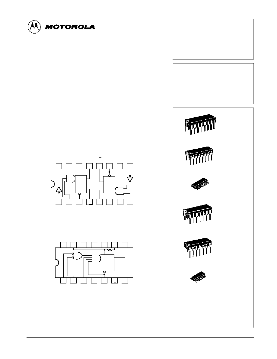
SN54 / 74LS122 (TOP VIEW)
(SEE NOTES 1 THRU 4)
SN54 / 74LS123 (TOP VIEW)
(SEE NOTES 1 THRU 4)
NOTES:
1. An external timing capacitor may be connected between Cext and Rext/Cext (positive).
2. To use the internal timing resistor of the LS122, connect Rint to VCC.
3. For improved pulse width accuracy connect an external resistor between Rext/Cext and
VCC with Rint open-circuited.
4. To obtain variable pulse widths, connect an external variable resistance between Rint/Cext
and VCC.
14
13
12
11
10
9
1
2
3
4
5
6
8
7
VCC
Rext/
Cext NC Cext NC Rint
Q
A1
A2
B1
B2
CLR
Q
GND
CLR Q
Q
Rint
2
Rext/
Cext
1
Cext
1 Rext/
Cext
14
13
12
11
10
9
1
2
3
4
5
6
7
16
15
8
VCC
1A
1Q
2Q
2B
2
CLR
2A
1B
1
CLR
1Q
2Q
2
Cext
GND
Q
Q
Q
Q
CLR
CLR
NC NO INTERNAL CONNECTION.
SN54/74LS122
SN54/74LS123
RETRIGGERABLE MONOSTABLE
MULTIVIBRATORS
LOW POWER SCHOTTKY
J SUFFIX
CERAMIC
CASE 620-09
N SUFFIX
PLASTIC
CASE 648-08
16
1
16
1
ORDERING INFORMATION
SN54LSXXXJ
Ceramic
SN74LSXXXN
Plastic
SN74LSXXXD
SOIC
16
1
D SUFFIX
SOIC
CASE 751B-03
J SUFFIX
CERAMIC
CASE 632-08
N SUFFIX
PLASTIC
CASE 646-06
14
1
14
1
14
1
D SUFFIX
SOIC
CASE 751A-02
5-198
FAST AND LS TTL DATA
SN54/74LS122
∑
SN54/74LS123
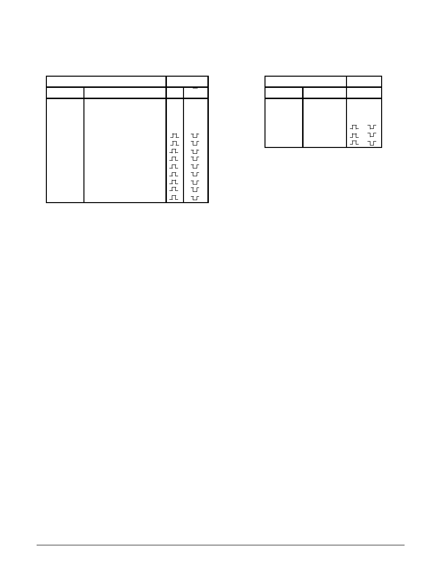
LS122
FUNCTIONAL TABLE
INPUTS
OUTPUTS
CLEAR
A1
A2
B1
B2
Q
Q
L
X
X
X
X
L
H
X
H
H
X
X
L
H
X
X
X
L
X
L
H
X
X
X
X
L
L
H
H
L
X
H
H
L
X
H
H
X
L
H
H
X
L
H
H
H
H
H
H
H
H
H
H
H
H
L
X
H
H
X
L
H
H
LS123
FUNCTIONAL TABLE
INPUTS
OUTPUTS
CLEAR
A
B
Q
Q
L
X
X
L
H
X
H
X
L
H
X
X
L
L
H
H
L
H
H
L
H
TYPICAL APPLICATION DATA
The output pulse tW is a function of the external compo-
nents, Cext and Rext or Cext and Rint on the LS122. For values
of Cext
1000 pF, the output pulse at VCC = 5.0 V and VRC =
5.0 V (see Figures 1, 2, and 3) is given by
tW = K Rext Cext where K is nominally 0.45
If Cext is on pF and Rext is in k
then tW is in nanoseconds.
The Cext terminal of the LS122 and LS123 is an internal
connection to ground, however for the best system perfor-
mance Cext should be hard-wired to ground.
Care should be taken to keep Rext and Cext as close to the
monostable as possible with a minimum amount of inductance
between the Rext/Cext junction and the Rext/Cext pin. Good
groundplane and adequate bypassing should be designed
into the system for optimum performance to insure that no
false triggering occurs.
It should be noted that the Cext pin is internally connected
to ground on the LS122 and LS123, but not on the LS221.
Therefore, if Cext is hard-wired externally to ground, substitu-
tion of a LS221 onto a LS123 socket will cause the LS221 to
become non-functional.
The switching diode is not needed for electrolytic capaci-
tance application and should not be used on the LS122 and
LS123.
To find the value of K for Cext
1000 pF, refer to Figure 4.
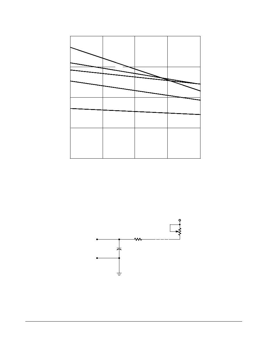
Variations on VCC or VRC can cause the value of K to change,
as can the temperature of the LS123, LS122. Figures 5 and
6 show the behavior of the circuit shown in Figures 1 and 2 if
separate power supplies are used for VCC and VRC. If VCC is
tied to VRC, Figure 7 shows how K will vary with VCC and
temperature. Remember, the changes in Rext and Cext with
temperature are not calculated and included in the graph.
As long as Cext
1000 pF and 5K
Rext
260K
(SN74LS122 / 123) or 5K
Rext
160 K (SN54LS122 / 123),
the change in K with respect to Rext is negligible.
If Cext
1000 pF the graph shown on Figure 8 can be used
to determine the output pulse width. Figure 9 shows how K will
change for Cext
1000 pF if VCC and VRC are connected to the
same power supply. The pulse width tW in nanoseconds is
approximated by
tW = 6 + 0.05 Cext (pF) + 0.45 Rext (k
) Cext + 11.6 Rext
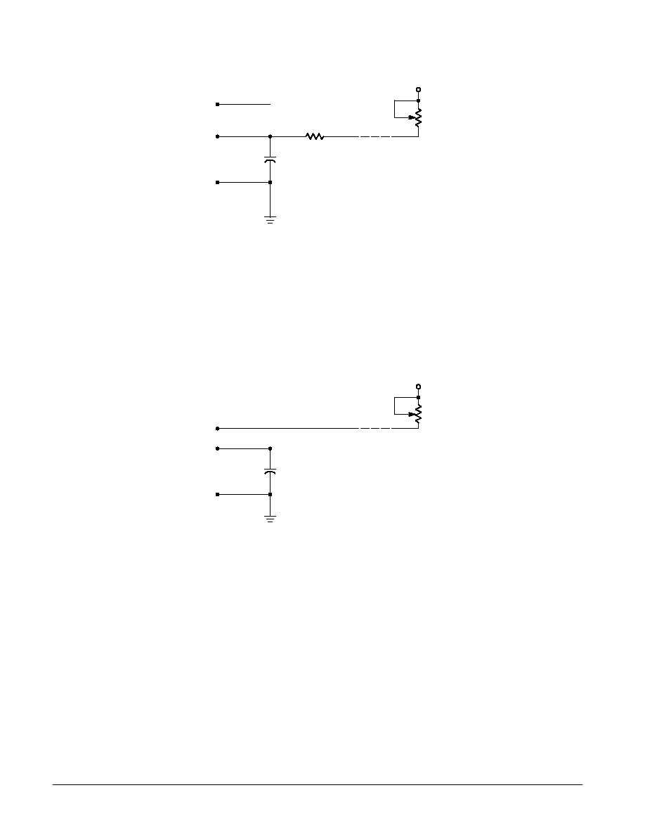
In order to trim the output pulse width, it is necessary to
include a variable resistor between VCC and the Rext/Cext pin
or between VCC and the Rext pin of the LS122. Figure 10, 11,
and 12 show how this can be done. Rext remote should be kept
as close to the monostable as possible.
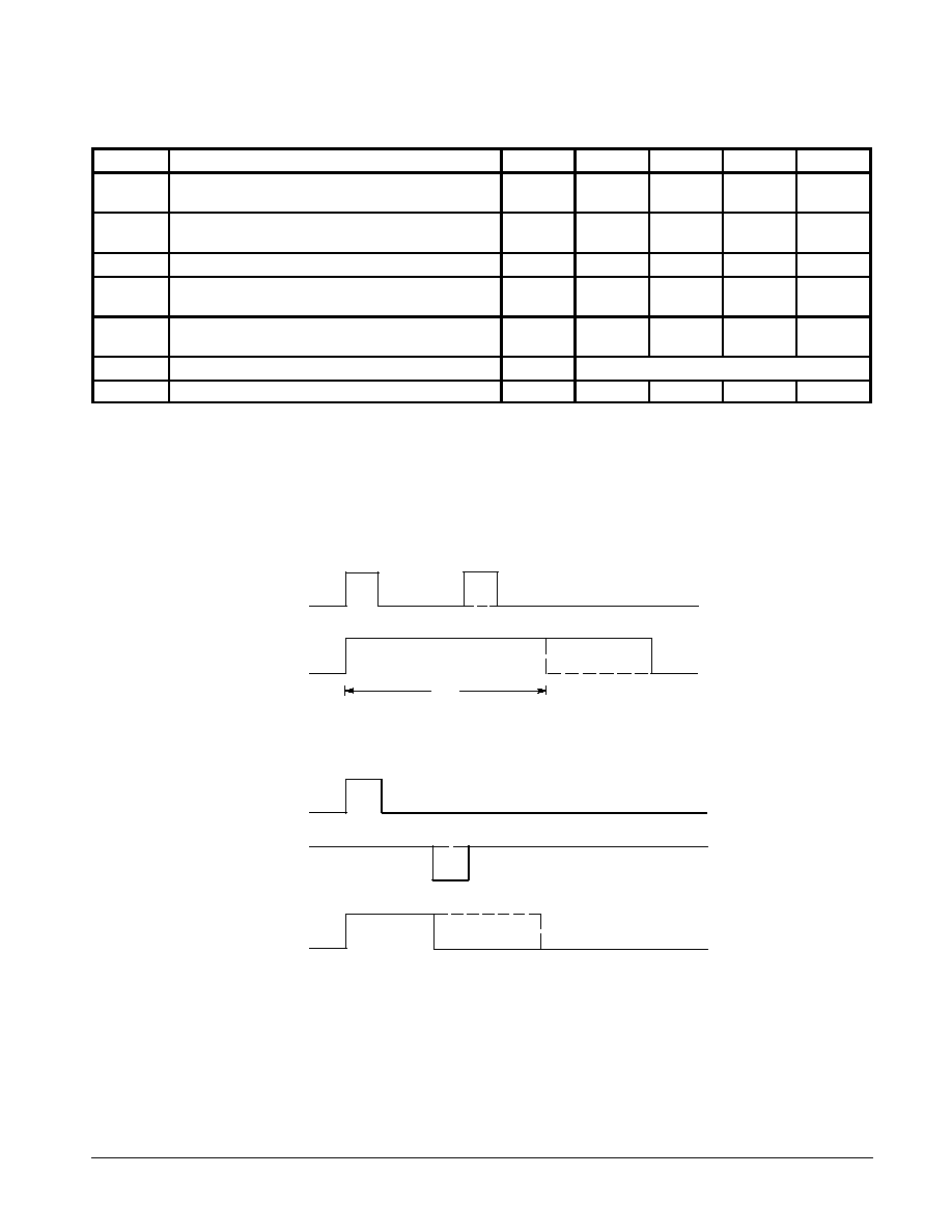
Retriggering of the part, as shown in Figure 3, must not
occur before Cext is discharged or the retrigger pulse will not
have any effect. The discharge time of Cext in nanoseconds is
guaranteed to be less than 0.22 Cext (pF) and is typically 0.05
Cext (pF).
For the smallest possible deviation in output pulse widths
from various devices, it is suggested that Cext be kept
1000 pF.
5-199
FAST AND LS TTL DATA
SN54/74LS122
∑
SN54/74LS123
GUARANTEED OPERATING RANGES
Symbol
Parameter
Min
Typ
Max
Unit
VCC
Supply Voltage
54
74
4.5
4.75
5.0
5.0
5.5
5.25
V
TA
Operating Ambient Temperature Range
54
74
≠ 55
0
25
25
125
70
∞
C
IOH
Output Current -- High
54, 74
≠ 0.4
mA
IOL
Output Current -- Low
54
74
4.0
8.0
mA
Rext
External Timing Resistance
54
74
5.0
5.0
180
260
k
Cext
External Capacitance
54, 74
No Restriction
Rext / Cext
Wiring Capacitance at Rext / Cext Terminal
54, 74
50
pF
WAVEFORMS
EXTENDING PULSE WIDTH
OVERRIDING THE OUTPUT PULSE
B INPUT
Q OUTPUT
B INPUT
CLEAR INPUT
CLEAR PULSE
Q OUTPUT
OUTPUT WITHOUT CLEAR PULSE
RETRIGGER
PULSE
(See Application Data)
OUTPUT WITHOUT RETRIGGER
tW
5-200
FAST AND LS TTL DATA
SN54/74LS122
∑
SN54/74LS123
DC CHARACTERISTICS OVER OPERATING TEMPERATURE RANGE
(unless otherwise specified)
Symbol
Parameter
Limits
Unit
Test Conditions
Symbol
Parameter
Min
Typ
Max
Unit
Test Conditions
VIH
Input HIGH Voltage
2.0
V
Guaranteed Input HIGH Voltage for
All Inputs
VIL
Input LOW Voltage
54
0.7
V
Guaranteed Input LOW Voltage for
All Inputs
VIL
Input LOW Voltage
74
0.8
V
Guaranteed Input LOW Voltage for
All Inputs
VIK
Input Clamp Diode Voltage
≠ 0.65
≠ 1.5
V
VCC = MIN, IIN = ≠ 18 mA
VOH
Output HIGH Voltage
54
2.5
3.5
V
VCC = MIN, IOH = MAX, VIN = VIH
or VIL per Truth Table
VOH
Output HIGH Voltage
74
2.7
3.5
V
VCC = MIN, IOH = MAX, VIN = VIH
or VIL per Truth Table
VOL
Output LOW Voltage
54, 74
0.25
0.4
V
IOL = 4.0 mA
VCC = VCC MIN,
VIN = VIL or VIH
per Truth Table
VOL
Output LOW Voltage
74
0.35
0.5
V
IOL = 8.0 mA
VIN = VIL or VIH
per Truth Table
IIH
Input HIGH Current
20
µ
A
VCC = MAX, VIN = 2.7 V
IIH
Input HIGH Current
0.1
mA
VCC = MAX, VIN = 7.0 V
IIL
Input LOW Current
≠ 0.4
mA
VCC = MAX, VIN = 0.4 V
IOS
Short Circuit Current (Note 1)
≠ 20
≠100
mA
VCC = MAX
ICC
Power Supply Current
LS122
11
mA
VCC = MAX
ICC
Power Supply Current
LS123
20
mA
VCC = MAX
Note 1: Not more than one output should be shorted at a time, nor for more than 1 second.
AC CHARACTERISTICS
(TA = 25
∞
C, VCC = 5.0 V)
Symbol
Parameter
Limits
Unit
Test Conditions
Symbol
Parameter
Min
Typ
Max
Unit
Test Conditions
tPLH
tPHL
Propagation Delay, A to Q
Propagation Delay, A to Q
23
33
ns
Cext = 0
CL = 15 pF
Rext = 5.0 k
RL = 2.0 k
tPLH
tPHL
Propagation Delay, A to Q
Propagation Delay, A to Q
32
45
ns
Cext = 0
CL = 15 pF
Rext = 5.0 k
RL = 2.0 k
tPLH
tPHL
Propagation Delay, B to Q
Propagation Delay, B to Q
23
44
ns
Cext = 0
CL = 15 pF
Rext = 5.0 k
RL = 2.0 k
tPLH
tPHL
Propagation Delay, B to Q
Propagation Delay, B to Q
34
56
ns
Rext = 5.0 k
RL = 2.0 k
tPLH
tPHL
Propagation Delay, Clear to Q
Propagation Delay, Clear to Q
28
45
ns
Rext = 5.0 k
RL = 2.0 k
tPLH
tPHL
Propagation Delay, Clear to Q
Propagation Delay, Clear to Q
20
27
ns
tW min
A or B to Q
116
200
ns
Cext = 1000 pF, Rext = 10 k
,
CL = 15 pF, RL = 2.0 k
tWQ
A to B to Q
4.0
4.5
5.0
µ
s
Cext = 1000 pF, Rext = 10 k
,
CL = 15 pF, RL = 2.0 k
AC SETUP REQUIREMENTS
(TA = 25
∞
C, VCC = 5.0 V)
Symbol
Parameter
Limits
Unit
Test Conditions
Symbol
Parameter
Min
Typ
Max
Unit
Test Conditions
tW
Pulse Width
40
ns
5-201
FAST AND LS TTL DATA
SN54/74LS122
∑
SN54/74LS123
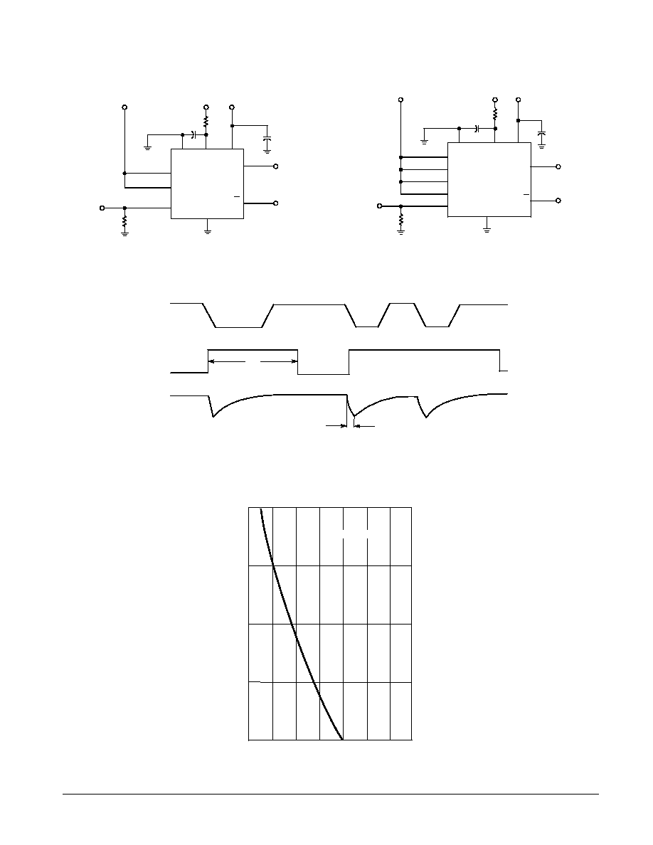
Figure 1
Figure 2
Figure 3
Figure 4
VCC
VRC
VCC
Cext
0.1
µ
F
Pout
Cext Rext/
Cext
VCC
Q
CLR
B
VCC
VCC
VRC
Rext
Cext
0.1
µ
F
Pout
51
Cext
Rext/
Cext
VCC
Q
CLR
B2
B1
A2
A1
GND
Q
1/2 LS123
LS122
Rext
Q
GND
A
51
Pin
Pin
Pin
Pout
tW
RETRIGGER
5K
Rext
260K
10
1
0.1
0.01
0.001
0.3
0.35 0.4
0.45 0.5
0.55
K
EXTERNAL
CAP
ACIT
ANCE, C ( F)
µ
ext

5-202
FAST AND LS TTL DATA
SN54/74LS122
∑
SN54/74LS123
Figure 8
Figure 5. K versus VCC
Figure 6. K versus VRC
Figure 7. K versus VCC and VRC
0.55
0.5
K
0.45
0.4
0.35
4.5
5
5.5
VCC
0.55
0.5
K
0.45
0.4
0.35
4.5
5
5.5
VCC = 5 V
Cext = 1000 pF
VRC
Cext = 1000 pF
0.55
0.5
K
0.45
0.4
0.35
4.5
5
5.5
VCC = VRC
125
∞
C
70
∞
C
25
∞
C
0
∞
C
- 55
∞
C
VRC = 5 V
Cext = 1000 pF
125
∞
C
70
∞
C
0
∞
C
- 55
∞
C
125
∞
C
25
∞
C
0
∞
C
- 55
∞
C
70
∞
C
25
∞
C
100000
10000
1000
100
10
1
10
100
1000
t W
Cext, EXTERNAL TIMING CAPACITANCE (pF)
Rext = 80 k
Rext = 40 k
Rext = 20 k
Rext = 10 k
Rext = 5 k
, OUTPUT
PULSE WIDTH (ns)
Rext = 260 k
Rext = 160 k
5-203
FAST AND LS TTL DATA
SN54/74LS122
∑
SN54/74LS123
Figure 9
Figure 10. LS123 Remote Trimming Circuit
Cext = 200 pF
0.65
0.6
K
0.55
0.5
4.5
4.75
5
5.25
5.5
VCC VOLTS
125
∞
C
70
∞
C
25
∞
C
0
∞
C
- 55
∞
C
VCC
Rext
REMOTE
Rext
Cext
PIN 7
OR 15
PIN 6
OR 14
5-204
FAST AND LS TTL DATA
SN54/74LS122
∑
SN54/74LS123
Figure 11. LS122 Remote Trimming Circuit Without Rext
Figure 12. LS122 Remote Trimming Circuit with Rint
OPEN
VCC
Rext
REMOTE
Rext
Cext
PIN 13
PIN 11
PIN 9
VCC
Rext
REMOTE
PIN 13
PIN 11
PIN 9
5-205
FAST AND LS TTL DATA
MIN
MIN
MAX
MAX
MILLIMETERS
INCHES
DIM
A
B
C
D
F
G
J
K
M
P
R
9.80
3.80
1.35
0.35
0.40
0.19
0.10
0
∞
5.80
0.25
10.00
4.00
1.75
0.49
1.25
0.25
0.25
7
∞
6.20
0.50
0.386
0.150
0.054
0.014
0.016
0.008
0.004
0
∞
0.229
0.010
0.393
0.157
0.068
0.019
0.049
0.009
0.009
7
∞
0.244
0.019
1.27 BSC
0.050 BSC
NOTES:
1. DIMENSIONING AND TOLERANCING PER ANSI
Y14.5M, 1982.
2. CONTROLLING DIMENSION: MILLIMETER.
3. DIMENSION A AND B DO NOT INCLUDE MOLD
PROTRUSION.
4. MAXIMUM MOLD PROTRUSION 0.15 (0.006)
PER SIDE.
5. 751B 01 IS OBSOLETE, NEW STANDARD
751B 03.
1
8
9
16
-A-
-B-
P
16 PL
D
-T-
K
C
G
M
R X 45
∞
F
J
8 PL
SEATING
PLANE
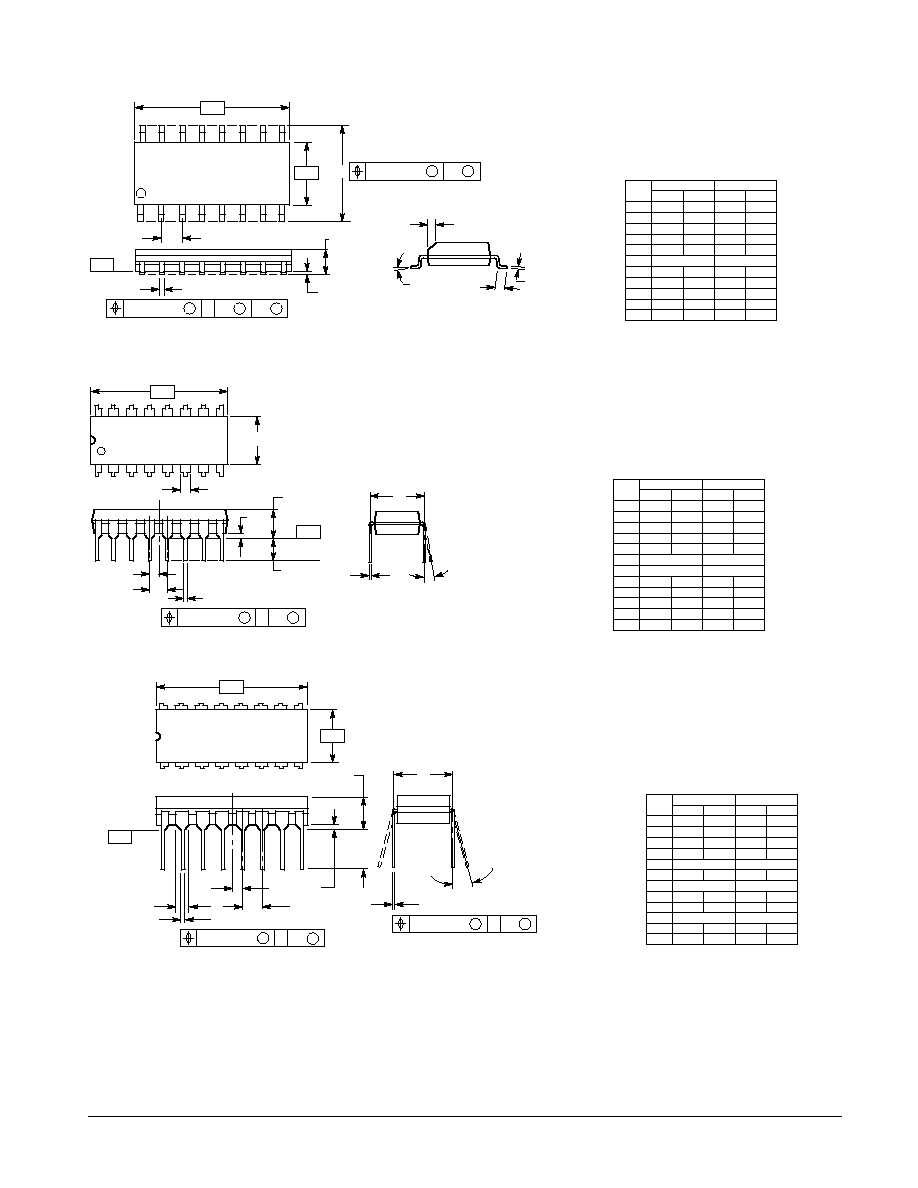
Case 751B-03 D Suffix
16-Pin Plastic
SO-16
B
0.25 (0.010)
M
M
T
0.25 (0.010)
B
A
M
S
S
Case 648-08 N Suffix
16-Pin Plastic
MIN
MIN
MAX
MAX
MILLIMETERS
INCHES
DIM
A
B
C
D
F
G
H
J
K
L
M
S
18.80
6.35
3.69
0.39
1.02
0.21
2.80
7.50
0
∞
0.51
19.55
6.85
4.44
0.53
1.77
0.38
3.30
7.74
10
∞
1.01
0.740
0.250
0.145
0.015
0.040
0.008
0.110
0.295
0
∞
0.020
0.770
0.270
0.175
0.021
0.070
0.015
0.130
0.305
10
∞
0.040
NOTES:
1. DIMENSIONING AND TOLERANCING PER ANSI
Y14.5M, 1982.
2. CONTROLLING DIMENSION: INCH.
3. DIMENSION L" TO CENTER OF LEADS WHEN
FORMED PARALLEL.
4. DIMENSION B" DOES NOT INCLUDE MOLD
FLASH.
5. ROUNDED CORNERS OPTIONAL.
6. 648 01 THRU 07 OBSOLETE, NEW STANDARD
648 08.
2.54 BSC
1.27 BSC
0.100 BSC
0.050 BSC
-A-
B
1
8
9
16
F
H
G
D
16 PL
S
C
-T-
SEATING
PLANE
K
J
M
L
T A
0.25 (0.010)
M
M
Case 620-09 J Suffix
16-Pin Ceramic Dual In-Line
MIN
MIN
MAX
MAX
MILLIMETERS
INCHES
DIM
19.05
6.10
0.39
1.40
0.23
0
∞
0.39
19.55
7.36
4.19
0.53
1.77
0.27
5.08
15
∞
0.88
0.750
0.240
0.015
0.055
0.009
0
∞
0.015
0.770
0.290
0.165
0.021
0.070
0.011
0.200
15
∞
0.035
1.27 BSC
2.54 BSC
7.62 BSC
0.050 BSC
0.100 BSC
0.300 BSC
A
B
C
D
E
F
G
J
K
L
M
N
NOTES:
1. DIMENSIONING AND TOLERANCING PER ANSI
Y14.5M, 1982.
2. CONTROLLING DIMENSION: INCH.
3. DIMENSION L TO CENTER OF LEAD WHEN
FORMED PARALLEL.
4. DIM F MAY NARROW TO 0.76 (0.030) WHERE
THE LEAD ENTERS THE CERAMIC BODY.
5. 620 01 THRU 08 OBSOLETE, NEW STANDARD
620 09.
-B-
-A-
16 PL
-T-
C
D
E
F
G
J
K
M
N
SEATING
PLANE
16 PL
L
16
9
1
8
0.25 (0.010)
T A
M
S
0.25 (0.010)
T B
M
S

5-206
FAST AND LS TTL DATA
Motorola reserves the right to make changes without further notice to any products herein. Motorola makes no warranty, representation or guarantee regarding
the suitability of its products for any particular purpose, nor does Motorola assume any liability arising out of the application or use of any product or circuit,
and specifically disclaims any and all liability, including without limitation consequential or incidental damages. "Typical" parameters can and do vary in different
applications. All operating parameters, including "Typicals" must be validated for each customer application by customer's technical experts. Motorola does
not convey any license under its patent rights nor the rights of others. Motorola products are not designed, intended, or authorized for use as components in
systems intended for surgical implant into the body, or other applications intended to support or sustain life, or for any other application in which the failure of
the Motorola product could create a situation where personal injury or death may occur. Should Buyer purchase or use Motorola products for any such
unintended or unauthorized application, Buyer shall indemnify and hold Motorola and its officers, employees, subsidiaries, affiliates, and distributors harmless
against all claims, costs, damages, and expenses, and reasonable attorney fees arising out of, directly or indirectly, any claim of personal injury or death
associated with such unintended or unauthorized use, even if such claim alleges that Motorola was negligent regarding the design or manufacture of the part.
Motorola and
are registered trademarks of Motorola, Inc. Motorola, Inc. is an Equal Opportunity/Affirmative Action Employer.
Literature Distribution Centers:
USA: Motorola Literature Distribution; P.O. Box 20912; Phoenix, Arizona 85036.
EUROPE: Motorola Ltd.; European Literature Centre; 88 Tanners Drive, Blakelands, Milton Keynes, MK14 5BP, England.
JAPAN: Nippon Motorola Ltd.; 4-32-1, Nishi-Gotanda, Shinagawa-ku, Tokyo 141, Japan.
ASIA PACIFIC: Motorola Semiconductors H.K. Ltd.; Silicon Harbour Center, No. 2 Dai King Street, Tai Po Industrial Estate, Tai Po, N.T., Hong Kong.