5-521
FAST AND LS TTL DATA
OCTAL TRANSPARENT LATCH
WITH 3-STATE OUTPUTS;
OCTAL D-TYPE FLIP-FLOP
WITH 3-STATE OUTPUT
The SN54 / 74LS373 consists of eight latches with 3-state outputs for bus
organized system applications. The flip-flops appear transparent to the data
(data changes asynchronously) when Latch Enable (LE) is HIGH. When LE is
LOW, the data that meets the setup times is latched. Data appears on the bus
when the Output Enable (OE) is LOW. When OE is HIGH the bus output is in
the high impedance state.
The SN54 / 74LS374 is a high-speed, low-power Octal D-type Flip-Flop fea-
turing separate D-type inputs for each flip-flop and 3-state outputs for bus ori-
ented applications. A buffered Clock (CP) and Output Enable (OE) is common
to all flip-flops. The SN54 / 74LS374 is manufactured using advanced Low
Power Schottky technology and is compatible with all Motorola TTL families.
∑
Eight Latches in a Single Package
∑
3-State Outputs for Bus Interfacing
∑
Hysteresis on Latch Enable
∑
Edge-Triggered D-Type Inputs
∑
Buffered Positive Edge-Triggered Clock
∑
Hysteresis on Clock Input to Improve Noise Margin
∑
Input Clamp Diodes Limit High Speed Termination Effects
PIN NAMES
LOADING (Note a)
HIGH
LOW
D0 ≠ D7
LE
CP
OE
O0 ≠ O7
Data Inputs
Latch Enable (Active HIGH) Input
Clock (Active HIGH going edge) Input
Output Enable (Active LOW) Input
Outputs (Note b)
0.5 U.L.
0.5 U.L.
0.5 U.L.
0.5 U.L.
65 (25) U.L.
0.25 U.L.
0.25 U.L.
0.25 U.L.
0.25 U.L.
15 (7.5) U.L.
NOTES:
a) 1 TTL Units Load (U.L.) = 40
µ
A HIGH/1.6 mA LOW.
b) The Output LOW drive factor is 7.5 U.L. for Military (54) and 25 U.L. for Commercial
(74) Temperature Ranges. The Output HIGH drive factor is 25 U.L. for Military (54) and
65 U.L. for Commercial (74) Temperature Ranges.
CONNECTION DIAGRAM DIP (TOP VIEW)
SN54 / 74LS373
SN54 / 74LS374
18
17
16
15
14
13
1
2
3
4
5
6
7
20
19
8
VCC
OE
O7 D7 D6 O6
D5
O5
D4
O0 D0 D1 O1 O2 D2 D3
9
10
O3 GND
12
O4 LE
18
17
16
15
14
13
1
2
3
4
5
6
7
20
19
8
VCC
OE
O7 D7 D6 O6
D5
O5
D4
O0 D0 D1 O1 O2 D2 D3
9
10
O3 GND
12
11
O4 CP
NOTE:
The Flatpak version
has the same pinouts
(Connection Diagram) as
the Dual In-Line Package.
11
SN54/74LS373
SN54/74LS374
OCTAL TRANSPARENT LATCH
WITH 3-STATE OUTPUTS;
OCTAL D-TYPE FLIP-FLOP
WITH 3-STATE OUTPUT
LOW POWER SCHOTTKY
ORDERING INFORMATION
SN54LSXXXJ
Ceramic
SN74LSXXXN
Plastic
SN74LSXXXDW SOIC
20
1
J SUFFIX
CERAMIC
CASE 732-03
20
1
N SUFFIX
PLASTIC
CASE 738-03
20
1
DW SUFFIX
SOIC
CASE 751D-03
5-522
FAST AND LS TTL DATA
SN54/74LS373
∑
SN54/74LS374
TRUTH TABLE
LS373
Dn
LE
OE
On
H
H
L
H
L
H
L
L
X
L
L
Q0
X
X
H
Z*
LS374
Dn
LE
OE
On
H
L
H
L
L
L
X
X
H
Z*
H = HIGH Voltage Level
L = LOW Voltage Level
X = Immaterial
Z = High Impedance
* Note: Contents of flip-flops unaffected by the state of the Output Enable input (OE).
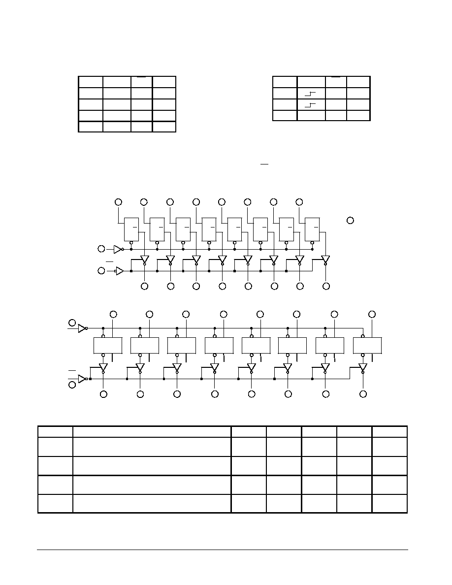
LOGIC DIAGRAMS
SN54LS / 74LS373
SN54LS / 74LS374
D
D
G
Q
CP
Q Q
CP
OE
OE
LE
LATCH
ENABLE
O0
O1
O2
O3
O4
O5
O6
O7
D0
14
1
2
6
7
3
8
4
5
9
11
12
16
13
15
VCC = PIN 20
GND = PIN 10
= PIN NUMBERS
D
G
Q
D1
D
G
Q
D2
D
G
Q
D3
D
G
Q
D4
D
G
Q
D5
D
G
Q
D6
D
G
Q
D7
17
18
19
O0
O1
O2
O3
O4
O5
O6
O7
2
6
5
9
12
16
15
19
D0
14
7
3
8
4
13
D1
D2
D3
D4
D5
D6
D7
17
18
1
11
D
CP
Q Q
D
CP
Q Q
D
CP
Q Q
D
CP
Q Q
D
CP
Q Q
D
CP
Q Q
D
CP
Q Q
GUARANTEED OPERATING RANGES
Symbol
Parameter
Min
Typ
Max
Unit
VCC
Supply Voltage
54
74
4.5
4.75
5.0
5.0
5.5
5.25
V
TA
Operating Ambient Temperature Range
54
74
≠ 55
0
25
25
125
70
∞
C
IOH
Output Current -- High
54
74
≠ 1.0
≠ 2.6
mA
IOL
Output Current -- Low
54
74
12
24
mA

5-523
FAST AND LS TTL DATA
SN54/74LS373
∑
SN54/74LS374
DC CHARACTERISTICS OVER OPERATING TEMPERATURE RANGE
(unless otherwise specified)
Symbol
Parameter
Limits
Unit
Test Conditions
Symbol
Parameter
Min
Typ
Max
Unit
Test Conditions
VIH
Input HIGH Voltage
2.0
V
Guaranteed Input HIGH Voltage for
All Inputs
VIL
Input LOW Voltage
54
0.7
V
Guaranteed Input LOW Voltage for
All Inputs
VIL
Input LOW Voltage
74
0.8
V
Guaranteed Input LOW Voltage for
All Inputs
VIK
Input Clamp Diode Voltage
≠ 0.65
≠ 1.5
V
VCC = MIN, IIN = ≠ 18 mA
VOH
Output HIGH Voltage
54
2.4
3.4
V
VCC = MIN, IOH = MAX, VIN = VIH
or VIL per Truth Table
VOH
Output HIGH Voltage
74
2.4
3.1
V
VCC = MIN, IOH = MAX, VIN = VIH
or VIL per Truth Table
VOL
Output LOW Voltage
54, 74
0.25
0.4
V
IOL = 12 mA
VCC = VCC MIN,
VIN = VIL or VIH
per Truth Table
VOL
Output LOW Voltage
74
0.35
0.5
V
IOL = 24 mA
VIN = VIL or VIH
per Truth Table
IOZH
Output Off Current HIGH
20
µ
A
VCC = MAX, VOUT = 2.7 V
IOZL
Output Off Current LOW
≠ 20
µ
A
VCC = MAX, VOUT = 0.4 V
IIH
Input HIGH Current
20
µ
A
VCC = MAX, VIN = 2.7 V
IIH
Input HIGH Current
0.1
mA
VCC = MAX, VIN = 7.0 V
IIL
Input LOW Current
≠ 0.4
mA
VCC = MAX, VIN = 0.4 V
IOS
Short Circuit Current (Note 1)
≠ 30
≠ 130
mA
VCC = MAX
ICC
Power Supply Current
40
mA
VCC = MAX
Note 1: Not more than one output should be shorted at a time, nor for more than 1 second.
AC CHARACTERISTICS
(TA = 25
∞
C, VCC = 5.0 V)
Symbol
Parameter
Limits
Unit
Test Conditions
Symbol
Parameter
LS373
LS374
Unit
Test Conditions
Symbol
Parameter
Min
Typ
Max
Min
Typ
Max
Unit
Test Conditions
fMAX
Maximum Clock Frequency
35
50
MHz
CL = 45 pF,
RL = 667
tPLH
tPHL
Propagation Delay,
Data to Output
12
12
18
18
ns
CL = 45 pF,
RL = 667
tPLH
tPHL
Clock or Enable
to Output
20
18
30
30
15
19
28
28
ns
CL = 45 pF,
RL = 667
tPZH
tPZL
Output Enable Time
15
25
28
36
20
21
28
28
ns
tPHZ
tPLZ
Output Disable Time
12
15
20
25
12
15
20
25
ns
CL = 5.0 pF
AC SETUP REQUIREMENTS
(TA = 25
∞
C, VCC = 5.0 V)
Symbol
Parameter
Limits
Unit
Symbol
Parameter
LS373
LS374
Unit
Symbol
Parameter
Min
Max
Min
Max
Unit
tW
Clock Pulse Width
15
15
ns
ts
Setup Time
5.0
20
ns
th
Hold Time
20
0
ns
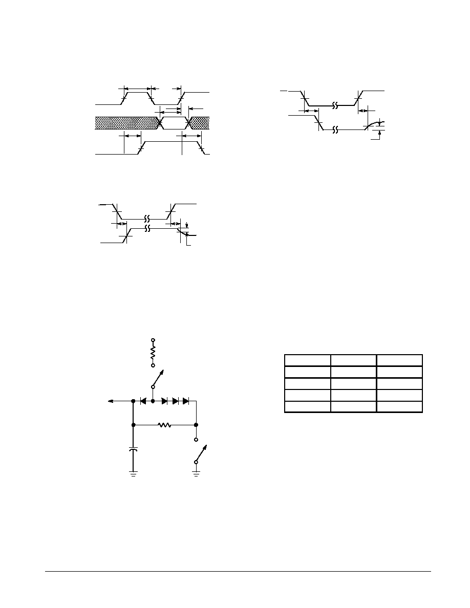
DEFINITION OF TERMS
SETUP TIME (ts) -- is defined as the minimum time required
for the correct logic level to be present at the logic input prior to
LE transition from HIGH-to-LOW in order to be recognized and
transferred to the outputs.
HOLD TIME (th) -- is defined as the minimum time following
the LE transition from HIGH-to-LOW that the logic level must
be maintained at the input in order to ensure continued
recognition.