
5-533
FAST AND LS TTL DATA
OCTAL D FLIP-FLOP WITH ENABLE;
HEX D FLIP-FLOP WITH ENABLE;
4-BIT D FLIP-FLOP WITH ENABLE
The SN54 / 74LS377 is an 8-bit register built using advanced Low Power
Schottky technology. This register consists of eight D-type flip-flops with a
buffered common clock and a buffered common clock enable.
The SN54 / 74LS378 is a 6-Bit Register with a buffered common enable.
This device is similar to the SN54 / 74LS174, but with common Enable rather
than common Master Reset.
The SN54 / 74LS379 is a 4-Bit Register with buffered common Enable. This
device is similar to the SN54 / 74LS175 but features the common Enable
rather then common Master Reset.
∑
8-Bit High Speed Parallel Registers
∑
Positive Edge-Triggered D-Type Flip Flops
∑
Fully Buffered Common Clock and Enable Inputs
∑
True and Complement Outputs
∑
Input Clamp Diodes Limit High Speed Termination Effects
PIN NAMES
LOADING (Note a)
HIGH
LOW
E
Enable (Active LOW) Input
0.5 U.L.
0.25 U.L.
D0 ≠ D3
Data Inputs
0.5 U.L.
0.25 U.L.
CP
Clock (Active HIGH Going Edge) Input
0.5 U.L.
0.25 U.L.
Q0 ≠ Q3
True Outputs (Note b)
10 U.L.
5 (2.5) U.L.
Q0 ≠ Q3
Complemented Outputs (Note b)
10 U.L.
5 (2.5) U.L.
NOTES:
a) 1 TTL Unit Load (U.L.) = 40
µ
A HIGH/1.6 mA LOW.
b) The Output LOW drive factor is 2.5 U.L. for Military (54) and 5 U.L. for Commercial
(74) Temperature Ranges.
SN54/74LS377
SN54/74LS378
SN54/74LS379
OCTAL D FLIP-FLOP WITH
ENABLE; HEX D FLIP-FLOP
WITH ENABLE; 4-BIT D FLIP-FLOP
WITH ENABLE
LOW POWER SCHOTTKY
ORDERING INFORMATION
SN54LSXXXJ
Ceramic
SN74LSXXXN
Plastic
SN74LSXXXDW SOIC
SN74LSXXXD
SOIC
J SUFFIX
CERAMIC
CASE 620-09
N SUFFIX
PLASTIC
CASE 648-08
16
1
16
1
16
1
D SUFFIX
SOIC
CASE 751B-03
20
1
J SUFFIX
CERAMIC
CASE 732-03
20
1
N SUFFIX
PLASTIC
CASE 738-03
20
1
DW SUFFIX
SOIC
CASE 751D-03

5-534
FAST AND LS TTL DATA
SN54/74LS377
∑
SN54/74LS378
∑
SN54/74LS379
CONNECTION DIAGRAM DIPS (TOP VIEW)
14
13
12
11
10
9
1
2
3
4
5
6
7
16
15
8
VCC
E
Q5
D5
D4
Q4
Q3
D3
CP
Q0
D0
D1
Q1
D2
Q2 GND
14
13
12
11
10
9
1
2
3
4
5
6
7
16
15
8
VCC
E
Q3
Q3
D3
D2
Q2
Q2
CP
Q0
Q0
D0
D1
Q1
Q1 GND
18
17
16
15
14
13
1
2
3
4
5
6
7
20
19
8
VCC
E
Q7 D7 D6 Q6
D5
Q5
D4
Q0 D0 D1 Q1 Q2 D2 D3
9
10
Q3 GND
12
11
Q4 CP
SN54 / 74LS377
SN54 / 74LS378
SN54 / 74LS379
NOTE:
The Flatpak version
has the same pinouts
(Connection Diagram) as
the Dual In-Line Package.
NOTE:
The Flatpak version
has the same pinouts
(Connection Diagram) as
the Dual In-Line Package.
NOTE:
The Flatpak version
has the same pinouts
(Connection Diagram) as
the Dual In-Line Package.

5-535
FAST AND LS TTL DATA
SN54/74LS377
∑
SN54/74LS378
∑
SN54/74LS379
LOGIC DIAGRAMS
SN54 / 74LS377
SN54 / 74LS378
SN54 / 74LS379
E
ENABLE
D0
D1
D2
D3
D4
D5
D6
D7
Q0
Q1
Q2
Q3
Q4
Q5
Q6
Q7
D0
D1
D2
D3
D4
D5
Q0
Q1
Q2
Q3
Q4
Q5
D0
D1
D2
D3
Q0
Q0
Q1
Q1
Q2
Q2
Q3
Q3
CP
CLOCK
CP D
Q
CP D
Q
E
CP
E
CP
E
14
2
6
7
3
8
4
5
9
12
16
13
17
CP D
Q
CP D
Q
CP D
Q
CP D
Q
CP D
Q
CP D
Q
CP D
Q
18
15
19
1
11
14
1
2
6
7
3
4
5
9
11
12
10
13
15
CP D
Q
E
CP D
Q
E
CP D
Q
E
CP D
Q
E
CP D
Q
E
CP
D
Q
E
Q
CP
D
Q
E
Q
CP
D
Q
E
Q
CP
D
Q
E
Q
14
1
2
6
7
3
4
5
9
11
12
10
13
15
5-536
FAST AND LS TTL DATA
SN54/74LS377
∑
SN54/74LS378
∑
SN54/74LS379
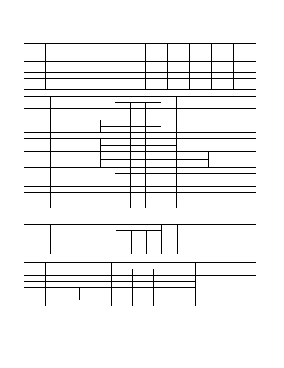
GUARANTEED OPERATING RANGES
Symbol
Parameter
Min
Typ
Max
Unit
VCC
Supply Voltage
54
74
4.5
4.75
5.0
5.0
5.5
5.25
V
TA
Operating Ambient Temperature Range
54
74
≠ 55
0
25
25
125
70
∞
C
IOH
Output Current -- High
54, 74
≠ 0.4
mA
IOL
Output Current -- Low
54
74
4.0
8.0
mA
DC CHARACTERISTICS OVER OPERATING TEMPERATURE RANGE
(unless otherwise specified)
Symbol
Parameter
Limits
Unit
Test Conditions
Symbol
Parameter
Min
Typ
Max
Unit
Test Conditions
VIH
Input HIGH Voltage
2.0
V
Guaranteed Input HIGH Voltage for
All Inputs
VIL
Input LOW Voltage
54
0.7
V
Guaranteed Input LOW Voltage for
VIL
Input LOW Voltage
74
0.8
V
Guaranteed Input LOW Voltage for
All Inputs
VIK
Input Clamp Diode Voltage
≠ 0.65
≠ 1.5
V
VCC = MIN, IIN = ≠ 18 mA
VOH
Output HIGH Voltage
54
2.5
3.5
V
VCC = MIN, IOH = MAX, VIN = VIH
or VIL per Truth Table
VOH
Output HIGH Voltage
74
2.7
3.5
V
VCC = MIN, IOH = MAX, VIN = VIH
or VIL per Truth Table
VOL
Output LOW Voltage
54, 74
0.25
0.4
V
IOL = 4.0 mA
VCC = VCC MIN,
VIN = VIL or VIH
per Truth Table
VOL
Output LOW Voltage
74
0.35
0.5
V
IOL = 8.0 mA
VIN = VIL or VIH
per Truth Table
IIH
Input HIGH Current
20
µ
A
VCC = MAX, VIN = 2.7 V
IIH
Input HIGH Current
0.1
mA
VCC = MAX, VIN = 7.0 V
IIL
Input LOW Current
≠ 0.4
mA
VCC = MAX, VIN = 0.4 V
IOS
Short Circuit Current (Note 1)
≠ 20
≠ 100
mA
VCC = MAX
ICC
Power Supply Current
LS377
LS378
LS379
28
22
15
mA
VCC = MAX, NOTE 1
NOTE: With all inputs open and GND applied to all data and enable inputs, ICC is measured after a momentary GND, then 4.5 V is applied to clock.
Note 1: Not more than one output should be shorted at a time, nor for more than 1 second.
AC CHARACTERISTICS
(TA = 25
∞
C, VCC = 5.0 V)
Symbol
Parameter
Limits
Unit
Test Conditions
Symbol
Parameter
Min
Typ
Max
Unit
Test Conditions
fMAX
Maximum Clock Frequency
30
40
MHz
VCC = 5.0 V
CL = 15 pF
tPLH
tPHL
Propagation Delay,
Clock to Output
17
18
27
27
ns
VCC = 5.0 V
CL = 15 pF
AC SETUP REQUIREMENTS
(TA = 25
∞
C, VCC = 5.0 V)
Symbol
Parameter
Limits
Unit
Test Conditions
Symbol
Parameter
Min
Typ
Max
Unit
Test Conditions
tW
Any Pulse Width
20
ns
VCC = 5.0 V
ts
Data Setup Time
20
ns
VCC = 5.0 V
ts
Enable Setup
Inactive -- State
10
ns
VCC = 5.0 V
ts
Enable Setup
Time
Active -- State
25
ns
CC = 5.0 V
th
Any Hold Time
5.0
ns
DEFINITION OF TERMS
SETUP TIME (ts) -- is defined as the minimum time required
for the correct logic level to be present at the logic input prior to
the clock transition from LOW-to-HIGH in order to be recog-
nized and transferred to the outputs.
HOLD TIME (th) -- is defined as the minimum time following
the clock transition from LOW-to-HIGH that the logic level
must be maintained at the input in order to ensure continued
recognition. A negative HOLD TIME indicates that the correct
logic level may be released prior to the clock transition from
LOW-to-HIGH and still be recognized.

5-537
FAST AND LS TTL DATA
SN54/74LS377
∑
SN54/74LS378
∑
SN54/74LS379
TRUTH TABLE
E
CP
Dn
Qn
Qn
H
X
No
Change
No
Change
L
H
H
L
L
L
L
H
L = LOW Voltage Level
H = HIGH Voltage Level
X = Immaterial
AC WAVEFORMS
SN54 / 74LS377
SN54 / 74LS378
SN54 / 74LS379
1.3 V
*The shaded areas indicate when the input is permitted to change for predictable output performance.
1.3 V
1.3 V
1.3 V
1.3 V
1.3 V
1/fmax
tW
ts(H)
th(H)
ts(L)
th(L)
CP
tPLH
tPHL
E, D
Q
*
1.3 V
1.3 V
1.3 V
1.3 V
1.3 V
1.3 V
1/fmax
tW
ts(H)
th(H)
ts(L)
th(L)
CP
tPHL
tPLH
D OR E
Q
*
1.3 V
1.3 V
1.3 V
1.3 V
1.3 V
1.3 V
1/fmax
tW
ts(H)
th(H)
ts(L)
th(L)
CP
tPHL
tPLH
E, D
Q
*
Figure 1. Clock to Output Delays Clock Pulse
Width, Frequency, Setup and Hold Times Data
or Enable to Clock
Figure 2. Clock to Output Delays Clock Pulse
Width, Frequency, Setup and Hold Times Data
or Enable to Clock
Figure 3. Clock to Output Delays Clock Pulse
Width, Frequency, Setup and Hold Times Data,
Enable to Clock

5-538
FAST AND LS TTL DATA
MIN
MIN
MAX
MAX
MILLIMETERS
INCHES
DIM
A
B
C
D
F
G
J
K
M
P
R
9.80
3.80
1.35
0.35
0.40
0.19
0.10
0
∞
5.80
0.25
10.00
4.00
1.75
0.49
1.25
0.25
0.25
7
∞
6.20
0.50
0.386
0.150
0.054
0.014
0.016
0.008
0.004
0
∞
0.229
0.010
0.393
0.157
0.068
0.019
0.049
0.009
0.009
7
∞
0.244
0.019
1.27 BSC
0.050 BSC
NOTES:
1. DIMENSIONING AND TOLERANCING PER ANSI
Y14.5M, 1982.
2. CONTROLLING DIMENSION: MILLIMETER.
3. DIMENSION A AND B DO NOT INCLUDE MOLD
PROTRUSION.
4. MAXIMUM MOLD PROTRUSION 0.15 (0.006)
PER SIDE.
5. 751B 01 IS OBSOLETE, NEW STANDARD
751B 03.
1
8
9
16
-A-
-B-
P
16 PL
D
-T-
K
C
G
M
R X 45
∞
F
J
8 PL
SEATING
PLANE
Case 751B-03 D Suffix
16-Pin Plastic
SO-16
B
0.25 (0.010)
M
M
T
0.25 (0.010)
B
A
M
S
S
Case 648-08 N Suffix
16-Pin Plastic
MIN
MIN
MAX
MAX
MILLIMETERS
INCHES
DIM
A
B
C
D
F
G
H
J
K
L
M
S
18.80
6.35
3.69
0.39
1.02
0.21
2.80
7.50
0
∞
0.51
19.55
6.85
4.44
0.53
1.77
0.38
3.30
7.74
10
∞
1.01
0.740
0.250
0.145
0.015
0.040
0.008
0.110
0.295
0
∞
0.020
0.770
0.270
0.175
0.021
0.070
0.015
0.130
0.305
10
∞
0.040
NOTES:
1. DIMENSIONING AND TOLERANCING PER ANSI
Y14.5M, 1982.
2. CONTROLLING DIMENSION: INCH.
3. DIMENSION L" TO CENTER OF LEADS WHEN
FORMED PARALLEL.
4. DIMENSION B" DOES NOT INCLUDE MOLD
FLASH.
5. ROUNDED CORNERS OPTIONAL.
6. 648 01 THRU 07 OBSOLETE, NEW STANDARD
648 08.
2.54 BSC
1.27 BSC
0.100 BSC
0.050 BSC
-A-
B
1
8
9
16
F
H
G
D
16 PL
S
C
-T-
SEATING
PLANE
K
J
M
L
T A
0.25 (0.010)
M
M
Case 620-09 J Suffix
16-Pin Ceramic Dual In-Line
MIN
MIN
MAX
MAX
MILLIMETERS
INCHES
DIM
19.05
6.10
0.39
1.40
0.23
0
∞
0.39
19.55
7.36
4.19
0.53
1.77
0.27
5.08
15
∞
0.88
0.750
0.240
0.015
0.055
0.009
0
∞
0.015
0.770
0.290
0.165
0.021
0.070
0.011
0.200
15
∞
0.035
1.27 BSC
2.54 BSC
7.62 BSC
0.050 BSC
0.100 BSC
0.300 BSC
A
B
C
D
E
F
G
J
K
L
M
N
NOTES:
1. DIMENSIONING AND TOLERANCING PER ANSI
Y14.5M, 1982.
2. CONTROLLING DIMENSION: INCH.
3. DIMENSION L TO CENTER OF LEAD WHEN
FORMED PARALLEL.
4. DIM F MAY NARROW TO 0.76 (0.030) WHERE
THE LEAD ENTERS THE CERAMIC BODY.
5. 620 01 THRU 08 OBSOLETE, NEW STANDARD
620 09.
-B-
-A-
16 PL
-T-
C
D
E
F
G
J
K
M
N
SEATING
PLANE
16 PL
L
16
9
1
8
0.25 (0.010)
T A
M
S
0.25 (0.010)
T B
M
S
5-539
FAST AND LS TTL DATA
Motorola reserves the right to make changes without further notice to any products herein. Motorola makes no warranty, representation or guarantee regarding
the suitability of its products for any particular purpose, nor does Motorola assume any liability arising out of the application or use of any product or circuit,
and specifically disclaims any and all liability, including without limitation consequential or incidental damages. "Typical" parameters can and do vary in different
applications. All operating parameters, including "Typicals" must be validated for each customer application by customer's technical experts. Motorola does
not convey any license under its patent rights nor the rights of others. Motorola products are not designed, intended, or authorized for use as components in
systems intended for surgical implant into the body, or other applications intended to support or sustain life, or for any other application in which the failure of
the Motorola product could create a situation where personal injury or death may occur. Should Buyer purchase or use Motorola products for any such
unintended or unauthorized application, Buyer shall indemnify and hold Motorola and its officers, employees, subsidiaries, affiliates, and distributors harmless
against all claims, costs, damages, and expenses, and reasonable attorney fees arising out of, directly or indirectly, any claim of personal injury or death
associated with such unintended or unauthorized use, even if such claim alleges that Motorola was negligent regarding the design or manufacture of the part.
Motorola and
are registered trademarks of Motorola, Inc. Motorola, Inc. is an Equal Opportunity/Affirmative Action Employer.
Literature Distribution Centers:
USA: Motorola Literature Distribution; P.O. Box 20912; Phoenix, Arizona 85036.
EUROPE: Motorola Ltd.; European Literature Centre; 88 Tanners Drive, Blakelands, Milton Keynes, MK14 5BP, England.
JAPAN: Nippon Motorola Ltd.; 4-32-1, Nishi-Gotanda, Shinagawa-ku, Tokyo 141, Japan.
ASIA PACIFIC: Motorola Semiconductors H.K. Ltd.; Silicon Harbour Center, No. 2 Dai King Street, Tai Po Industrial Estate, Tai Po, N.T., Hong Kong.