DSP56F826 Data Sheet
DSP56F826/D
Rev. 9.0, 04/2003
© Motorola, Inc., 2003. All rights reserved.
56F826
Technical Data
56F826 16-bit Hybrid Controller
·
Up to 40 MIPS at 80MHz core frequency
·
DSP and MCU functionality in a unified,
C-efficient architecture
·
Hardware DO and REP loops
·
MCU-friendly instruction set supports both
DSP and controller functions: MAC, bit
manipulation unit, 14 addressing modes
·
31.5K
× 16-bit words Program Flash
·
512
× 16-bit words Program RAM
·
2K
× 16-bit words Data Flash
·
4K
× 16-bit words Data RAM
·
2K
× 16-bit words BootFLASH
·
Up to 64K
× 16-bit words each of external
memory expansion for Program and Data
memory
·
One Serial Port Interface (SPI)
·
One additional SPI or two optional Serial
Communication Interfaces (SCI)
·
One Synchronous Serial Interface (SSI)
·
One General Purpose Quad Timer
·
JTAG/OnCE
TM
for debugging
·
100-pin LQFP Package
·
16 dedicated and 30 shared GPIO
·
Time-of-Day (TOD) Timer
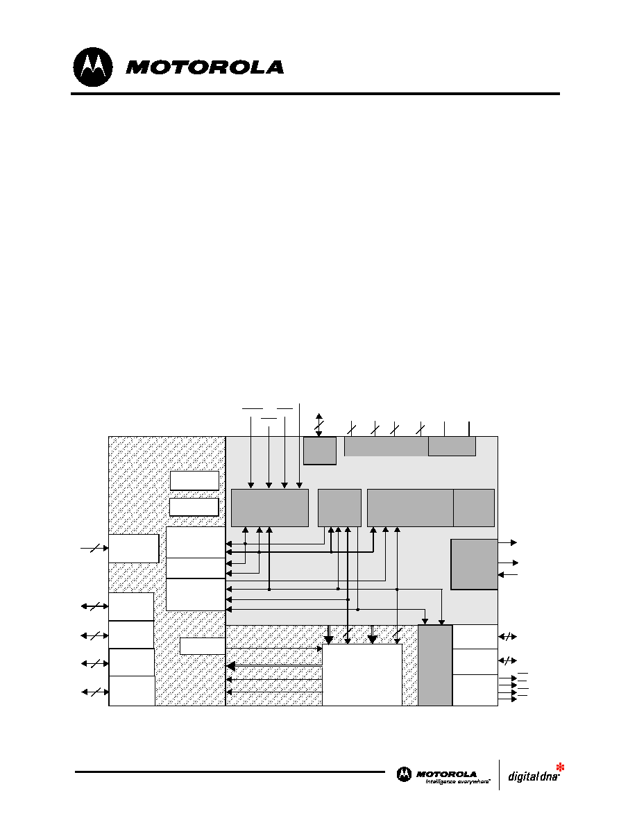
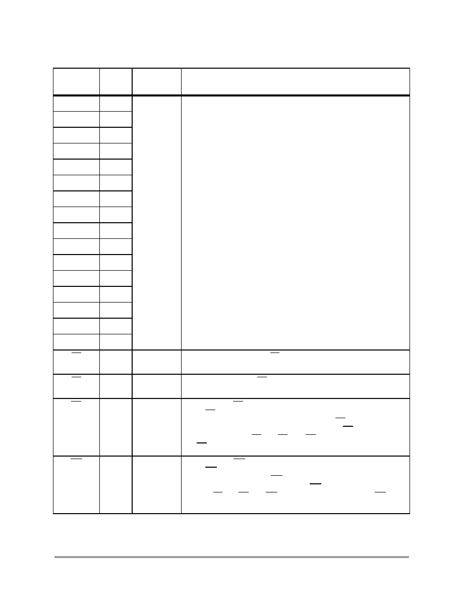
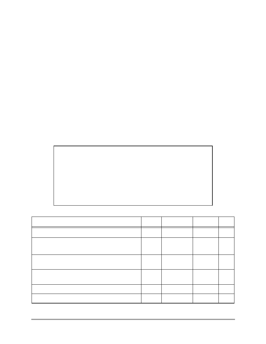
Figure 1. 56F826 Block Diagram
JTAG/
OnCE
Port
Program Controller
and
Hardware Looping Unit
Data ALU
16 x 16 + 36
36-Bit MAC
Three 16-bit Input Registers
Two 36-bit Accumulators
Address
Generation
Unit
Bit
Manipulation
Unit
PLL
Clock Gen
16-Bit
56800
Core
PAB
PDB
XDB2
CGDB
XAB1
XAB2
XTAL
EXTAL
INTERRUPT
CONTROLS
IPBB
CONTROLS
IPBus Bridge
(IPBB)
MODULE CONTROLS
ADDRESS BUS [8:0]
DATA BUS [15:0]
COP
RESET
Application-
Specific
Memory &
Peripherals
Interrupt
Controller
Program Memory
32252 x 16 Flash
512 x 16 SRAM
Boot Flash
2048 x 16 Flash
Data Memory
2048 x 16 Flash
4096 x 16 SRAM
COP/
Watchdog
SCI0 & SCI1
or
SPI0
SSI
or
GPIO
Quad Timer
or
GPIO
4
6
4
16
16
V
DDIO
V
SSIO
V
DDA
V
SSA
6
4
4
SPI1
or
GPIO
4
Dedicated
GPIO
16
External
Bus
Interface
Unit
External
Address Bus
Switch
Bus
Control
External
Data Bus
Switch
RD Enable
WR Enable
DS Select[1]
PS Select[0]
16
16
D[00:15]
A[00:15]
or
GPIO
CLKO
RESET
IRQA
IRQB
EXTBOOT
V
DD
V
SS
3
4
TOD
Timer
Low Voltage
Superviso
r
Analog Reg

2
56F826 Technical Data
MOTOROLA
Part 1 Overview
1.1 56F826 Features
1.1.1
Digital Signal Processing Core
·
Efficient 16-bit 56800 Family hybrid controller engine with dual Harvard architecture
·
As many as 40 Million Instructions Per Second (MIPS) at 80MHz core frequency
·
Single-cycle 16
× 16-bit parallel Multiplier-Accumulator (MAC)
·
Two 36-bit accumulators, including extension bits
·
16-bit bidirectional barrel shifter
·
Parallel instruction set with unique DSP addressing modes
·
Hardware DO and REP loops
·
Three internal address buses and one external address bus
·
Four internal data buses and one external data bus
·
Instruction set supports both DSP and controller functions
·
Controller style addressing modes and instructions for compact code
·
Efficient C Compiler and local variable support
·
Software subroutine and interrupt stack with depth limited only by memory
·
JTAG/OnCE Debug Programming Interface
1.1.2
Memory
·
Harvard architecture permits as many as three simultaneous accesses to Program and Data memory
·
On-chip memory including a low-cost, high-volume Flash solution
-- 31.5K
× 16-bit
words of Program Flash
-- 512
× 16-bit
words of Program RAM
-- 2K
× 16-bit
words of Data Flash
-- 4K
× 16-bit
words of Data RAM
-- 2K
× 16-bit
words of BootFLASH
·
Off-chip memory expansion capabilities programmable for 0, 4, 8, or 12 wait states
-- As much as 64 K
× 16-bit
Data memory
-- As much as 64 K
× 16-bit
Program memory
1.1.3
Peripheral Circuits for 56F826
·
One General Purpose Quad Timer totalling 7 pins
·
One Serial Peripheral Interface with 4 pins (or four additional GPIO lines)
·
One Serial Peripheral Interface, or multiplexed with two Serial Communications Interfaces
totalling 4 pins
·
Synchronous Serial Interface (SSI) with configurable six-pin port (or six additional GPIO lines)

56F826 Description
MOTOROLA
56F826 Technical Data
3
·
Sixteen (16) dedicated general purpose I/O (GPIO) pins
·
Thirty (30) shared general purpose I/O (GPIO) pins
·
Computer-Operating Properly (COP) Watchdog timer
·
Two external interrupt pins
·
External reset pin for hardware reset
·
JTAG/On-Chip Emulation (OnCETM) for unobtrusive, processor speed-independent debugging
·
Software-programmable, Phase Locked Loop-based frequency synthesizer for the hybrid controller
core clock
·
Fabricated in high-density EMOS with 5V-tolerant, TTL-compatible digital inputs
·
One Time of Day module
1.1.4
Energy Information
·
Dual power supply, 3.3V and 2.5V
·
Wait and Multiple Stop modes available
1.2 56F826 Description
The 56F826 is a member of the 56800 core-based family of hybrid controllers. It combines, on a single
chip, the processing power of a DSP and the functionality of a microcontroller with a flexible set of
peripherals to create an extremely cost-effective solution for general purpose applications. Because of its
low cost, configuration flexibility, and compact program code, the 56F826 is well-suited for many
applications. The 56F826 includes many peripherals that are especially useful for applications such as:
noise suppression, ID tag readers, sonic/subsonic detectors, security access devices, remote metering,
sonic alarms, POS terminals, feature phones.
The 56800 core is based on a Harvard-style architecture consisting of three execution units operating in
parallel, allowing as many as six operations per instruction cycle. The microprocessor-style programming
model and optimized instruction set allow straightforward generation of efficient, compact code for both
DSP and MCU applications. The instruction set is also highly efficient for C/C++ Compilers to enable rapid
development of optimized control applications.
The 56F826 supports program execution from either internal or external memories. Two data operands can
be accessed from the on-chip Data RAM per instruction cycle. The 56F826 also provides two external
dedicated interrupt lines, and up to 46 General Purpose Input/Output (GPIO) lines, depending on peripheral
configuration.
The 56F826 controller includes 31.5K words (16-bit) of Program Flash and 2K words of Data Flash (each
programmable through the JTAG port) with 512 words of Program RAM, and 4K words of Data RAM. It
also supports program execution from external memory.
The 56F826 incorporates a total of 2K words of Boot Flash for easy customer-inclusion of field-
programmable software routines that can be used to program the main Program and Data Flash memory
areas. Both Program and Data Flash memories can be independently bulk-erased or erased in page sizes of
256 words. The Boot Flash memory can also be either bulk or page erased.
This controller also provides a full set of standard programmable peripherals including one Synchronous
Serial Interface (SSI), one Serial Peripheral Interface (SPI), the option to select a second SPI or two Serial
Communications Interfaces (SCIs), and one Quad Timer. The SSI, SPI, and Quad Timer can be used as
General Purpose Input/Outputs (GPIOs) if a timer function is not required.

4
56F826 Technical Data
MOTOROLA
1.3 "Best in Class" Development Environment
The SDK (Software Development Kit) provides fully debugged peripheral drivers, libraries and interfaces
that allow a programmer to create their unique C application code independent of component architecture.
The CodeWarrior Integrated Development Environment is a sophisticated tool for code navigation,
compiling, and debugging. A complete set of evaluation modules (EVMs) and development system cards
will support concurrent engineering. Together, the SDK, CodeWarrior, and EVMs create a complete,
scalable tools solution for easy, fast, and efficient development.
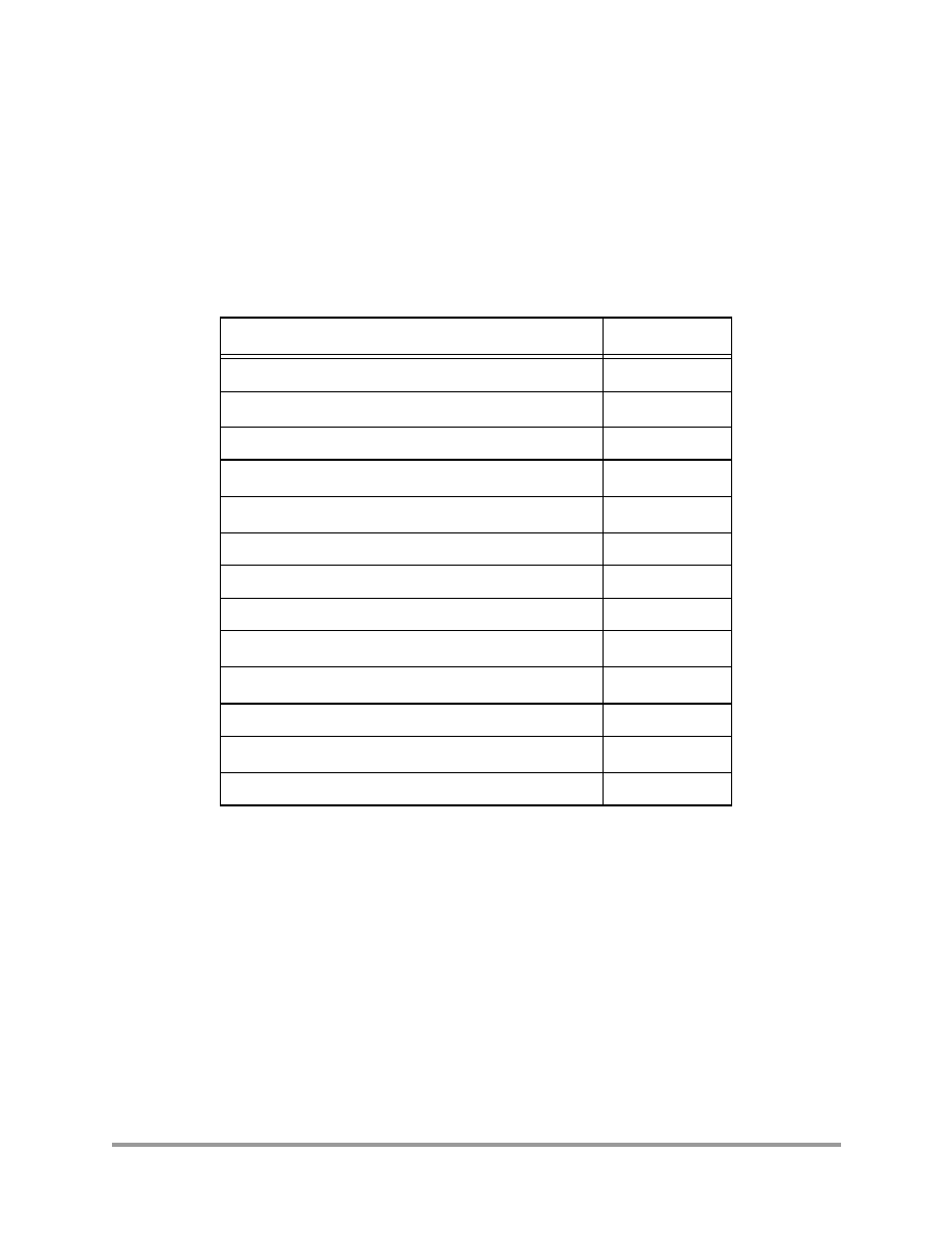
1.4 Product Documentation
The four documents listed in
Table 1
are required for a complete description and proper design with the
56F826. Documentation is available from local Motorola distributors, Motorola semiconductor sales
offices, Motorola Literature Distribution Centers, or online at www.motorola.com/dsp.
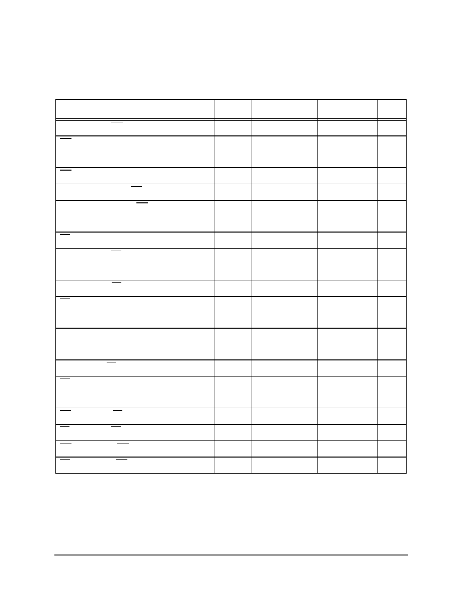
Table 1. 56F826 Chip Documentation
1.5 Data Sheet Conventions
This data sheet uses the following conventions:
Topic
Description
Order Number
DSP56800
Family Manual
Detailed description of the 56800 family architecture,
and 16-bit DSP core processor and the instruction set
DSP56800FM/D
DSP56F826/F827
User's Manual
Detailed description of memory, peripherals, and
interfaces of the 56F826 and 56F827
DSP56F826-827UM/D
DSP56F826
Technical Data Sheet
Electrical and timing specifications, pin descriptions,
and package descriptions (this document)
DSP56F826/D
DSP56F826
Product Brief
Summary description and block diagram of the 56F826
core, memory, peripherals and interfaces
DSP56F826PB/D
OVERBAR
This is used to indicate a signal that is active when pulled low. For example, the RESET pin is
active when low.
"asserted"
A high true (active high) signal is high or a low true (active low) signal is low.
"deasserted"
A high true (active high) signal is low or a low true (active low) signal is high.
Examples:
Signal/Symbol
Logic State
Signal State
Voltage
1
1.
Values for V
IL
, V
OL
, V
IH
, and V
OH
are defined by individual product specifications.
PIN
True
Asserted
V
IL
/V
OL
PIN
False
Deasserted
V
IH
/V
OH
PIN
True
Asserted
V
IH
/V
OH
PIN
False
Deasserted
V
IL
/V
OL
Introduction
MOTOROLA
56F826 Technical Data
5
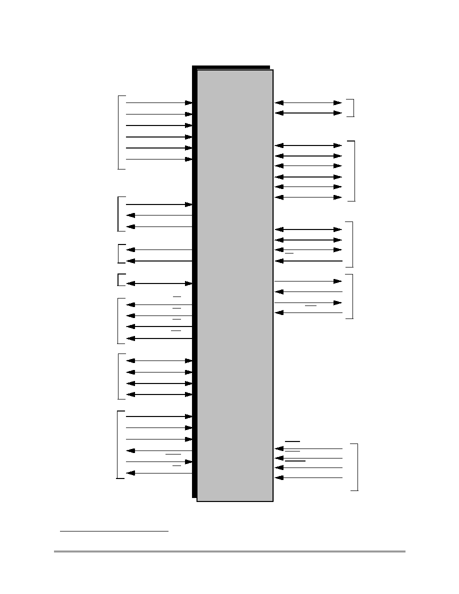
Part 2 Signal/Connection Descriptions
2.1 Introduction
The input and output signals of the 56F826 are organized into functional groups, as shown in
Table 2
and
as illustrated in
Figure 2
.
Table 3
describes the signal or signals present on a pin.
Table 2. Functional Group Pin Allocations
Functional Group
Number of Pins
Power (V
DD
, V
DDIO or
V
DDA
)
(3,4,1)
Ground (V
SS
, V
SSIO or
V
SSA
)
(3,4,1)
PLL and Clock
3
Address Bus
1
16
Data Bus
1
16
Bus Control
4
Interrupt and Program Control
5
Dedicated General Purpose Input/Output
16
Synchronous Serial Interface (SSI) Port
1
6
Serial Peripheral Interface (SPI) Port
1
1. Alternately,
GPIO
pins
4
Serial Communications Interface (SCI) Ports
4
Quad Timer Module Ports
1
4
JTAG/On-Chip Emulation (OnCE)
6
6
56F826 Technical Data
MOTOROLA
Figure 2. 56F826 Signals Identified by Functional Group
1
1. Alternate pin functionality is shown in parenthesis.
56F826
2.5V Power
Ground
3.3V Power
Ground
3.3V Analog Power
Analog Ground
PLL
and
Clock
External
Address Bus or
GPIO
External Data
Bus
External
Bus Control
Dedicated
GPIO
SPI1 Port
or GPIO
SCI0, SCI1
Port or
SPI0 Port
V
DD
V
SS
V
DDIO
V
SSIO
V
DDA
V
SSA
EXTAL
XTAL (CLOCKIN)
CLKO
A0-A7 (GPIOE)
A8-A15 (GPIOA)
D0D15
PS
DS
RD
WR
TA0 (GPIOF0)
TA1 (GPIOF1)
TA2 (GPIOF2)
TA3 (GPIOF3)
TCK
TMS
TDI
TDO
TRST
DE
Quad Timer A
or GPIO
JTAG/OnCE
Port
GPIOB07
GPIOD07
SRD (GPIOC0)
SRFS (GPIOC1)
SRCK (GPIOC2)
STD (GPIOC3)
STFS (GPIOC4)
STCK (GPIOC5)
SCLK (GPIOF4)
MOSI (GPIOF5)
MISO (GPIOF6)
SS (GPIOF7)
TXD0 (SCLK0)
RXD0 (MOSI0)
TXD1 (MISO0)
RXD1 (SS0)
IRQA
IRQB
RESET
EXTBOOT
SSI Port
or GPIO
3
4
4
4
1
1
1
1
1
8
8
16
1
1
1
1
1
1
1
1
1
1
1
1
1
1
Interrupt/
Program
Control
8
8
1
1
1
1
1
1
1
1
1
1
1
1
1
1
1
1
1
1
Signals and Package Information
MOTOROLA
56F826 Technical Data
7
2.2 Signals and Package Information
All inputs have a weak internal pull-up circuit associated with them. These pull-up circuits are always
enabled. Exceptions:
1. When a pin is owned by GPIO, then the pull-up may be disabled under software control.
2. TCK has a weak pull-down circuit always active.
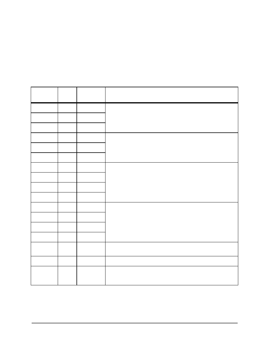
Table 3. 56F826 Signal and Package Information for the 100 Pin LQFP
Signal
Name
Pin No.
Type
Description
V
DD
20
V
DD
Power--These pins provide power to the internal structures of the chip,
and are generally connected to a 2.5V supply.
V
DD
64
V
DD
V
DD
94
V
DD
V
SS
19
V
SS
GND--These pins provide grounding for the internal structures of the
chip. All should be attached to V
SS.
V
SS
63
V
SS
V
SS
95
V
SS
V
DDIO
5
V
DDIO
Power In/Out--These pins provide power to the I/O structures of the
chip, and are generally connected to a 3.3V supply.
V
DDIO
30
V
DDIO
V
DDIO
57
V
DDIO
V
DDIO
80
V
DDIO
V
SSIO
6
V
SSIO
GND In/Out--These pins provide grounding for the I/O ring on the chip.
All should be attached to V
SS.
V
SSIO
31
V
SSIO
V
SSIO
58
V
SSIO
V
SSIO
81
V
SSIO
V
DDA
59
V
DDA
Analog Power--This pin is a dedicated power pin for the analog portion
of the chip and should be connected to a low noise 3.3V supply.
V
SSA
60
V
SSA
Analog Ground--This pin supplies an analog ground.
EXTAL
61
Input
External Crystal Oscillator Input--This input should be connected to
an 4MHz external crystal or ceramic resonator. For more information,
please refer to
Section 3.6
.

8
56F826 Technical Data
MOTOROLA
XTAL
(CLOCKIN)
62
Output
Input
Crystal Oscillator Output--This output connects the internal crystal
oscillator output to an external crystal or ceramic resonator. If an external
clock source over 4MHz is used, XTAL must be used as the input and
EXTAL connected to
V
SS. For more information, please refer to
Section
3.6.3
.
External Clock Input--This input should be asserted when using an
external clock or ceramic resonator.
CLKO
65
Output
Clock Output--This pin outputs a buffered clock signal. By programming
the CLKO Select Register CSLKOSR), the user can select between
outputting a version of the signal applied to XTAL and a version of the
device master clock at the output of the PLL. The clock frequency on this
pin can be disabled by programming the CLKO Select Register
(CLKOSR).
A0
(GPIOE0)
24
Output
Input/Output
Address Bus--A0A7 specify the address for external program or data
memory accesses.
Port E GPIO--These eight General Purpose I/O (GPIO) pins can be
individually programmed as input or output pins.
After reset, the default state is Address Bus.
A1
(GPIOE1)
23
A2
(GPIOE2)
22
A3
(GPIOE3)
21
A4
(GPIOE4)
18
A5
(GPIOE5)
17
A6
(GPIOE6)
16
A7
(GPIOE7)
15
Table 3. 56F826 Signal and Package Information for the 100 Pin LQFP
Signal
Name
Pin No.
Type
Description

Signals and Package Information
MOTOROLA
56F826 Technical Data
9
A8
(GPIOA0)
14
Output
Input/Output
Address Bus--A8A15 specify the address for external program or data
memory accesses.
Port A GPIO--These eight General Purpose I/O (GPIO) pins can be
individually programmed as input or output pins.
After reset, the default state is Address Bus.
A9
(GPIOA1)
13
A10
(GPIOA2)
12
A11
(GPIOA3)
11
A12
(GPIOA4)
10
A13
(GPIOA5)
9
A14
(GPIOA6)
8
A15
(GPIOA7)
7
Table 3. 56F826 Signal and Package Information for the 100 Pin LQFP
Signal
Name
Pin No.
Type
Description
10
56F826 Technical Data
MOTOROLA
D0
34
Input/Output
Data Bus-- D0D15 specify the data for external program or data memory
accesses. D0D15 are tri-stated when the external bus is inactive.
D1
35
D2
36
D3
37
D4
38
D5
39
D6
40
D7
41
D8
42
D9
43
D10
44
D11
46
D12
47
D13
48
D14
49
D15
50
PS
29
Output
Program Memory Select--PS is asserted low for external program
memory access.
DS
28
Output
Data Memory Select--DS is asserted low for external data memory
access.
RD
26
Output
Read Enable--RD is asserted during external memory read cycles.
When RD is asserted low, pins D0D15 become inputs and an external
device is enabled onto the device data bus. When RD is deasserted high,
the external data is latched inside the device. When RD is asserted, it
qualifies the A0A15, PS, and DS pins. RD can be connected directly to
the OE pin of a Static RAM or ROM.
WR
27
Output
Write Enable--WR is asserted during external memory write cycles.
When WR is asserted low, pins D0D15 become outputs and the device
puts data on the bus. When WR is deasserted high, the external data is
latched inside the external device. When WR is asserted, it qualifies the
A0A15, PS, and DS pins. WR can be connected directly to the WE pin of
a Static RAM.
Table 3. 56F826 Signal and Package Information for the 100 Pin LQFP
Signal
Name
Pin No.
Type
Description
Signals and Package Information
MOTOROLA
56F826 Technical Data
11
TA0-0
(GPIOF0)
91
Input/Output
Input/Output
TA03--Timer F Channels 0, 1, 2, and 3
Port F GPIO--These four General Purpose I/O (GPIO) pins can be
individually programmed as input or output.
After reset, the default state is Quad Timer.
TA0-1
(GPIOF1)
90
TA0-2
(GPIOF2)
89
TA0-3
(GPIOF3)
88
TCK
100
Input
(Schmitt)
Test Clock Input--This input pin provides a gated clock to synchronize
the test logic and shift serial data to the JTAG/OnCE port. The pin is
connected internally to a pull-down resistor.
TMS
1
Input
(Schmitt)
Test Mode Select Input--This input pin is used to sequence the JTAG
TAP controller's state machine. It is sampled on the rising edge of TCK
and has an on-chip pull-up resistor.
TDI
2
Input
(Schmitt)
Test Data Input--This input pin provides a serial input data stream to the
JTAG/OnCE port. It is sampled on the rising edge of TCK and has an on-
chip pull-up resistor.
TDO
3
Output
Test Data Output--This tri-statable output pin provides a serial output
data stream from the JTAG/OnCE port. It is driven in the Shift-IR and
Shift-DR controller states, and changes on the falling edge of TCK.
TRST
4
Input
(Schmitt)
Test Reset--As an input, a low signal on this pin provides a reset signal
to the JTAG TAP controller. To ensure complete hardware reset, TRST
should be asserted whenever RESET is asserted. The only exception
occurs in a debugging environment when a hardware device reset is
required and it is necessary not to reset the JTAG/OnCE module. In this
case, assert RESET, but do not assert TRST.
DE
98
Output
Debug Event--DE provides a low pulse on recognized debug events.
TCS
99
Input/Output
(Schmitt)
TCS--This pin is reserved for factory use. It must be tied to V
SS
for
normal use. In block diagrams, this pin is considered an additional V
SS.
Table 3. 56F826 Signal and Package Information for the 100 Pin LQFP
Signal
Name
Pin No.
Type
Description
12
56F826 Technical Data
MOTOROLA
GPIOB0
66
Input or
Output
Port B GPIO--These eight dedicated General Purpose I/O (GPIO) pins
can be individually programmed as input or output pins.
After reset, the default state is GPIO input.
GPIOB1
67
GPIOB2
68
GPIOB3
69
GPIOB4
70
GPIOB5
71
GPIOB6
72
GPIOB7
73
GPIOD0
74
Input or
Output
Port D GPIO--These eight dedicated GPIO pins can be individually
programmed as an input or output pins.
After reset, the default state is GPIO input.
GPIOD1
75
GPIOD2
76
GPIOD3
77
GPIOD4
78
GPIOD5
79
GPIOD6
82
GPIOD7
83
SRD
(GPIOC0)
51
Input/Output
Input/Output
SSI Receive Data (SRD)--This input pin receives serial data and
transfers the data to the SSI Receive Shift Receiver.
Port C GPIO--This is a General Purpose I/O (GPIO) pin with the
capability of being individually programmed as input or output.
After reset, the default state is GPIO input.
SRFS
(GPIOC1)
52
Input/ Output
Input/Output
SSI Serial Receive Frame Sync (SRFS)--This bidirectional pin is used
by the receive section of the SSI as frame sync I/O or flag I/O. The STFS
can be used only by the receiver. It is used to synchronize data transfer
and can be an input or an output.
Port C GPIO--This is a General Purpose I/O (GPIO) pin with the
capability of being individually programmed as input or output.
After reset, the default state is GPIO input.
Table 3. 56F826 Signal and Package Information for the 100 Pin LQFP
Signal
Name
Pin No.
Type
Description

Signals and Package Information
MOTOROLA
56F826 Technical Data
13
SRCK
(GPIOC2)
53
Input/Output
Input/Output
SSI Serial Receive Clock (SRCK)--This bidirectional pin provides the
serial bit rate clock for the Receive section of the SSI. The clock signal
can be continuous or gated and can be used by both the transmitter and
receiver in synchronous mode.
Port C GPIO--This is a General Purpose I/O (GPIO) pin with the
capability of being individually programmed as input or output.
After reset, the default state is GPIO input.
STD
(GPIOC3)
54
Output
Input/Output
SSI Transmit Data (STD)--This output pin transmits serial data from the
SSI Transmitter Shift Register.
Port C GPIO--This is a General Purpose I/O (GPIO) pin with the
capability of being individually programmed as input or output.
After reset, the default state is GPIO input.
STFS
(GPIOC4)
55
Input
Input/Output
SSI Serial Transmit Frame Sync (STFS)--This bidirectional pin is used
by the Transmit section of the SSI as frame sync I/O or flag I/O. The
STFS can be used by both the transmitter and receiver in synchronous
mode. It is used to synchronize data transfer and can be an input or
output pin.
Port C GPIO--This is a General Purpose I/O (GPIO) pin with the
capability of being individually programmed as input or output.
After reset, the default state is GPIO input.
STCK
(GPIOC5)
56
Input/ Output
Input/Output
SSI Serial Transmit Clock (STCK)--This bidirectional pin provides the
serial bit rate clock for the transmit section of the SSI. The clock signal
can be continuous or gated. It can be used by both the transmitter and
receiver in synchronous mode.
Port C GPIO--This is a General Purpose I/O (GPIO) pin with the
capability of being individually programmed as input or output.
After reset, the default state is GPIO input.
SCLK
(GPIOF4)
84
Input/Output
Input/Output
SPI Serial Clock--In master mode, this pin serves as an output, clocking
slaved listeners. In slave mode, this pin serves as the data clock input.
Port F GPIO--This General Purpose I/O (GPIO) pin can be individually
programmed as input or output.
After reset, the default state is SCLK.
Table 3. 56F826 Signal and Package Information for the 100 Pin LQFP
Signal
Name
Pin No.
Type
Description

14
56F826 Technical Data
MOTOROLA
MOSI
(GPIOF5)
85
Input/Output
Input/Output
SPI Master Out/Slave In (MOSI)--This serial data pin is an output from a
master device and an input to a slave device. The master device places
data on the MOSI line a half-cycle before the clock edge that the slave
device uses to latch the data.
Port F GPIO--This General Purpose I/O (GPIO) pin can be individually
programmed as input or output.
MISO
(GPIOF6)
86
Input/Output
Input/Output
SPI Master In/Slave Out (MISO)--This serial data pin is an input to a
master device and an output from a slave device. The MISO line of a
slave device is placed in the high-impedance state if the slave device is
not selected.
Port F GPIO--This General Purpose I/O (GPIO) pin can be individually
programmed as input or output.
After reset, the default state is MISO.
SS
(GPIOF7)
87
Input
Input/Output
SPI Slave Select--In master mode, this pin is used to arbitrate multiple
masters. In slave mode, this pin is used to select the slave.
Port F GPIO--This General Purpose I/O (GPIO) pin can be individually
programmed as input or output.
After reset, the default state is SS.
TXD0
(SCLK0)
97
Output
Input/Output
Transmit Data (TXD0)--transmit data output
SPI Serial Clock--In master mode, this pin serves as an output, clocking
slaved listeners. In slave mode, this pin serves as the data clock input.
After reset, the default state is SCI output.
RXD0
(MOSI0)
96
Input
Input/
Output
Receive Data (RXD0)-- receive data input
SPI Master Out/Slave In--This serial data pin is an output from a master
device, and an input to a slave device. The master device places data on
the MOSI line one half-cycle before the clock edge the slave device uses
to latch the data.
After reset, the default state is SCI input.
TXD1
(MISO0)
93
Output
Input/Output
Transmit Data (TXD1)--transmit data output
SPI Master In/Slave Out--This serial data pin is an input to a master
device and an output from a slave device. The MISO line of a slave
device is placed in the high-impedance state if hte slave device is not
selected.
After reset, the default state is SCI output.
Table 3. 56F826 Signal and Package Information for the 100 Pin LQFP
Signal
Name
Pin No.
Type
Description
Signals and Package Information
MOTOROLA
56F826 Technical Data
15
RXD1
(SS0)
92
Input
(Schmitt)
Input
Receive Data (RXD1)-- receive data input
SPI Slave Select--In master mode, this pin is used to arbitrate multiple
masters. In slave mode, this pin is used to select the slave.
After reset, the default state is SCI input.
IRQA
32
Input
(Schmitt)
External Interrupt Request A--The IRQA input is a synchronized
external interrupt request that indicates that an external device is
requesting service. It can be programmed to be level-sensitive or
negative-edge- triggered. If level-sensitive triggering is selected, an
external pull up resistor is required for wired-OR operation.
If the processor is in the Stop state and IRQA is asserted, the processor
will exit the Stop state.
IRQB
33
Input
(Schmitt)
External Interrupt Request B--The IRQB input is an external interrupt
request that indicates that an external device is requesting service. It can
be programmed to be level-sensitive or negative-edge-triggered. If level-
sensitive triggering is selected, an external pull up resistor is required for
wired-OR operation.
RESET
45
Input
(Schmitt)
Reset--This input is a direct hardware reset on the processor. When
RESET is asserted low, the device is initialized and placed in the Reset
state. A Schmitt trigger input is used for noise immunity. When the
RESET pin is deasserted, the initial chip operating mode is latched from
the external boot pin. The internal reset signal will be deasserted
synchronous with the internal clocks, after a fixed number of internal
clocks.
To ensure complete hardware reset, RESET and TRST should be
asserted together. The only exception occurs in a debugging
environment when a hardware device reset is required and it is
necessary not to reset the OnCE/JTAG module. In this case, assert
RESET, but do not assert TRST.
EXTBOOT
25
Input
(Schmitt)
External Boot--This input is tied to V
DD
to force device to boot from off-
chip memory. Otherwise, it is tied to ground.
Table 3. 56F826 Signal and Package Information for the 100 Pin LQFP
Signal
Name
Pin No.
Type
Description
16
56F826 Technical Data
MOTOROLA
Part 3 Specifications
3.1 General Characteristics
The 56F826 is fabricated in high-density CMOS with 5V-tolerant TTL-compatible digital inputs. The term
"5V-tolerant" refers to the capability of an I/O pin, built on a 3.3V compatible process technology, to
withstand a voltage up to 5.5V without damaging the device. Many systems have a mixture of devices
designed for 3.3V and 5V power supplies. In such systems, a bus may carry both 3.3V and 5V-compatible
I/O voltage levels. A standard 3.3V I/O is designed to receive a maximum voltage of 3.3V
± 10% during
normal operation without causing damage. This 5V-tolerant capability, therefore, offers the power savings
of 3.3V I/O levels while being able to receive 5V levels without being damaged.
Absolute maximum ratings given in
Table 4
are stress ratings only, and functional operation at the
maximum is not guaranteed. Stress beyond these ratings may affect device reliability or cause permanent
damage to the device.
The 56F826 DC/AC electrical specifications are preliminary and are from design simulations. These
specifications may not be fully tested or guaranteed at this early stage of the product life cycle. Finalized
specifications will be published after complete characterization and device qualifications have been
completed.
CAUTION
This device contains protective circuitry to guard against
damage due to high static voltage or electrical fields.
However, normal precautions are advised to avoid
application of any voltages higher than maximum rated
voltages to this high-impedance circuit. Reliability of
operation is enhanced if unused inputs are tied to an
appropriate voltage level.
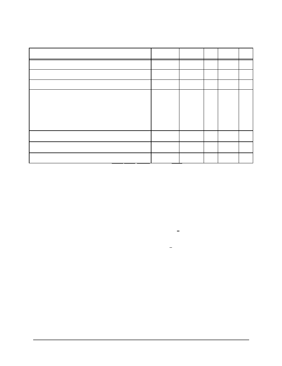
Table 4. Absolute Maximum Ratings
Characteristic
Symbol
Min
Max
Unit
Supply voltage, core
V
DD
1
1. V
DD
must not exceed V
DDIO
V
SS
0.3
V
SS
+ 3.0
V
Supply voltage, IO
Supply voltage, Analog
V
DDIO
2
V
DDA
2
2. V
DDIO
and V
DDA
must not differ by more that 0.5V
V
SSIO
0.3
V
SSA
0.3
V
SSIO
+ 4.0
V
SSA
+ 4.0
V
Digital input voltages
Analog input voltages - XTAL, EXTAL
V
IN
V
INA
V
SSIO
0.3
V
SSA
0.3
V
SSIO
+ 5.5
V
DDA
+ 0.3
V
Current drain per pin excluding V
DD
, V
SS,
V
DDA
, V
SSA,
V
DDIO
, V
SSIO
I
--
10
mA
Junction temperature
T
J
--
150
°C
Storage temperature range
T
STG
55
150
°C
General Characteristics
MOTOROLA
56F826 Technical Data
17
Notes:
1.
Theta-JA determined on 2s2p test boards is frequently lower than would be observed in an application.
Determined on 2s2p thermal test board.
2.
Junction to ambient thermal resistance, Theta-JA (
R
JA
) was simulated to be equivalent to the
JEDEC specification JESD51-2 in a horizontal configuration in natural convection. Theta-JA was
also simulated on a thermal test board with two internal planes (2s2p where "s" is the number of
signal layers and "p" is the number of planes) per JESD51-6 and JESD51-7. The correct name for
Theta-JA for forced convection or with the non-single layer boards is Theta-JMA.
3.
Junction to case thermal resistance, Theta-JC (R
JC
), was simulated to be equivalent to the
measured values using the cold plate technique with the cold plate temperature used as the "case"
temperature. The basic cold plate measurement technique is described by MIL-STD 883D, Method
1012.1. This is the correct thermal metric to use to calculate thermal performance when the package
is being used with a heat sink.
4.
Thermal Characterization Parameter, Psi-JT (
JT
), is the "resistance" from junction to reference
point thermocouple on top center of case as defined in JESD51-2.
JT
is a useful value to use to
estimate junction temperature in steady state customer environments.
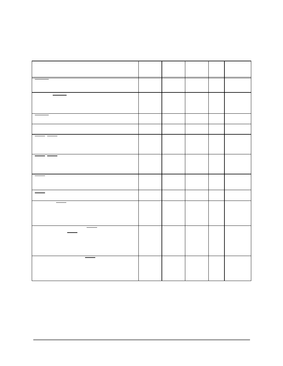
Table 5. Recommended Operating Conditions
Characteristic
Symbol
Min
Typ
Max
Unit
Supply voltage, core
V
DD
2.4
2.5
2.75
V
Supply Voltage, IO and analog
V
DDIO,
V
DDA
3.0
3.3
3.6
V
Ambient operating temperature
T
A
40
85
°C
Table 6. Thermal Characteristics
6
Characteristic
Comments
Symbol
Value
Unit
Notes
100-pin LQFP
Junction to ambient
Natural convection
R
JA
48.3
°C/W
2
Junction to ambient (@1m/sec)
R
JMA
43.9
°C/W
2
Junction to ambient
Natural convection
Four layer board (2s2p)
R
JMA
(2s2p)
40.7
°C/W
1.2
Junction to ambient (@1m/sec)
Four layer board (2s2p)
R
JMA
38.6
°C/W
1,2
Junction to case
R
JC
13.5
°C/W
3
Junction to center of case
JT
1.0
°C/W
4, 5
I/O pin power dissipation
P
I/O
User Determined
W
Power dissipation
P
D
P
D
= (I
DD
x V
DD
+ P
I/O
)
W
Junction to center of case
P
DMAX
(TJ - TA) /
JA
°C
18
56F826 Technical Data
MOTOROLA
5.
Junction temperature is a function of on-chip power dissipation, package thermal resistance,
mounting site (board) temperature, ambient temperature, air flow, power dissipation of other
components on the board, and board thermal resistance.
6.
See Section 5.1 from more details on thermal design considerations.
3.2 DC Electrical Characteristics
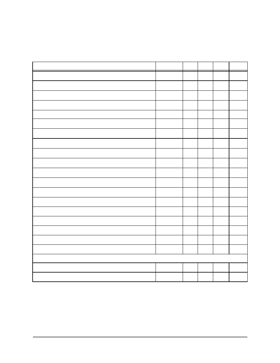
Table 7. DC Electrical Characteristics
Operating Conditions:
V
SSIO
=V
SS
= V
SSA
= 0V, V
DDA
=V
DDIO
=3.03.6V, V
DD
= 2.252.75V, T
A
= 40
° to +85°C, C
L
50pF, f
op
= 80MHz
Characteristic
Symbol
Min
Typ
Max
Unit
Input high voltage (XTAL/EXTAL)
V
IHC
2.25
--
3.6
V
Input low voltage (XTAL/EXTAL)
V
ILC
0
--
0.5
V
Input high voltage (Schmitt trigger inputs)
1
V
IHS
2.2
--
5.5
V
Input low voltage (Schmitt trigger inputs)
1
V
ILS
-0.3
--
0.8
V
Input high voltage (all other digital inputs)
V
IH
2.0
--
5.5
V
Input low voltage (all other digital inputs)
V
IL
-0.3
--
0.8
V
Input current high (pull-up/pull-down resistors disabled,
V
IN
=V
DD
)
I
IH
-1
--
1
µ
A
Input current low (pull-up/pull-down resistors disabled,
V
IN
=V
SS
)
I
IL
-1
--
1
µ
A
Input current high (with pull-up resistor, V
IN
=V
DD
)
I
IHPU
-1
--
1
µ
A
Input current low (with pull-up resistor, V
IN
=V
SS
)
I
ILPU
-210
--
-50
µ
A
Input current high (with pull-down resistor, V
IN
=V
DD
)
I
IHPD
20
--
180
µ
A
Input current low (with pull-down resistor, V
IN
=V
SS
)
I
ILPD
-1
--
1
µ
A
Nominal pull-up or pull-down resistor value
R
PU
, R
PD
30
K
Output tri-state current low
I
OZL
-10
--
10
µ
A
Output tri-state current high
I
OZH
-10
--
10
µ
A
Input current high (analog inputs, V
IN
=V
DDA
)
2
I
IHA
-15
--
15
µ
A
Input current low (analog inputs, V
IN
=V
SSA
)
2
I
ILA
-15
--
15
µ
A
Output High Voltage (at IOH)
V
OH
V
DD
0.7
--
--
V
Output Low Voltage (at IOL)
V
OL
--
--
0.4
V
Output source current
I
OH
4
--
--
mA
Output sink current
I
OL
4
--
--
mA
PWM pin output source current
3
I
OHP
10
--
--
mA
DC Electrical Characteristics
MOTOROLA
56F826 Technical Data
19
PWM pin output sink current
4
I
OLP
16
--
--
mA
Input capacitance
C
IN
--
8
--
pF
Output capacitance
C
OUT
--
12
--
pF
V
DD
supply current
I
DDT
5
Run
6
--
47
75
mA
Wait
7
--
21
36
mA
Stop
--
2
8
mA
Low Voltage Interrupt, V
DDIO
power supply
8
V
EIO
2.4
2.7
3.0
V
Low Voltage Interrupt, V
DD
power supply
9
V
EIC
2.0
2.2
2.4
V
Power on Reset
10
V
POR
--
1.7
2.0
V
1.
Schmitt Trigger inputs are: EXTBOOT, IRQA, IRQB, RESET, TCS, TCK, TRST, TMS, TDI and RXD1
2.
Analog inputs are: ANA[0:7], XTAL and EXTAL. Specification assumes ADC is not sampling.
3.
PWM pin output source current measured with 50% duty cycle.
4.
PWM pin output sink current measured with 50% duty cycle.
5. I
DDT
= I
DD
+ I
DDA
(Total supply current for V
DD
+ V
DDA
)
6. Run (operating) I
DD
measured using 8MHz clock source. All inputs 0.2V from rail; outputs unloaded. All ports
configured as inputs; measured with all modules enabled.
7. Wait
I
DD
measured using external square wave clock source (f
osc
= 8MHz) into XTAL; all inputs 0.2V from rail; no DC
loads; less than 50pF on all outputs. C
L
= 20pF on EXTAL; all ports configured as inputs; EXTAL capacitance linearly affects
wait I
DD
; measured with PLL enabled.
8. This low-voltage interrupt monitors the V
DDIO
power supply. If V
DDIO
drops below V
EIO
, an interrupt is generated.
Functionality of the device is guaranteed under transient conditions when V
DDIO
>V
EIO
(between the minimum specified
V
DDIO
and the point when the V
EIO
interrupt is generated).
9. This low-voltage interrupt monitors theV
DD
power supply. If V
DDIO
drops below V
EIC
, an interrupt is generated.
Functionality of the device is guaranteed under transient conditions when V
DD
>V
EIC
(between the minimum specified V
DD
and the point when the V
EIC
interrupt is generated).
10. Power
on reset occurs whenever the V
DD
power supply drops below
V
POR
. While power is ramping up, this signal
remains active for as long as V
DD
is below
V
POR
no matter how long the ramp-up rate is.
Table 7. DC Electrical Characteristics (Continued)
Operating Conditions:
V
SSIO
=V
SS
= V
SSA
= 0V, V
DDA
=V
DDIO
=3.03.6V, V
DD
= 2.252.75V, T
A
= 40
° to +85°C, C
L
50pF, f
op
= 80MHz
Characteristic
Symbol
Min
Typ
Max
Unit
20
56F826 Technical Data
MOTOROLA
Figure 3. Maximum Run IDD vs. Frequency (see Note
6.
in
Table 7
)
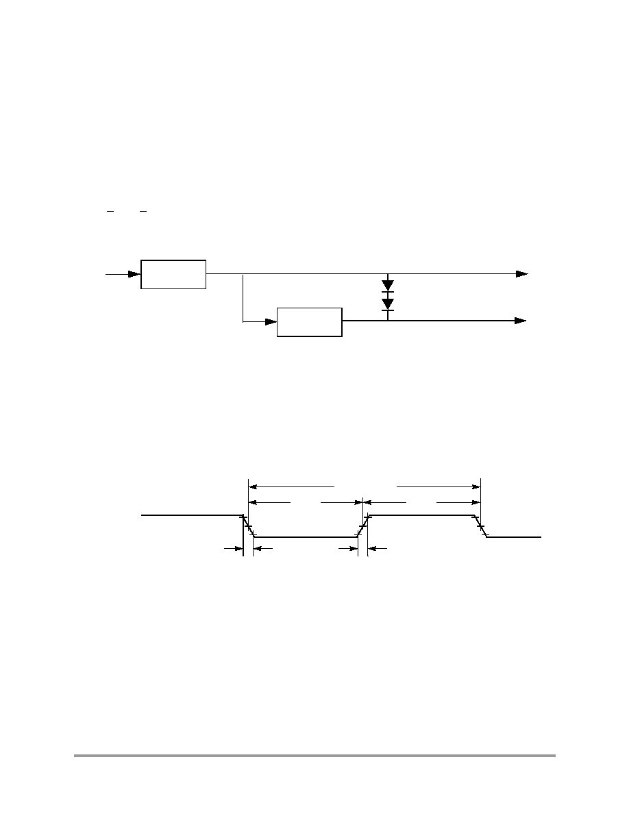
3.3 Supply Voltage Sequencing and Separation Cautions
Figure 4
shows two situations to avoid in sequencing the V
DD
and V
DDIO,
V
DDA
supplies.
Notes: 1. V
DD
rising before V
DDIO
, V
DDA
2. V
DDIO
, V
DDA
rising much faster than V
DD
Figure 4. Supply Voltage Sequencing and Separation Cautions
0
25
75
100
50
20
40
60
80
Freq. (MHz)
I
D
D (mA)
IDD Digital
IDD Analog
IDD Total
3.3V
2.5V
Time
0
2
1
Supplies Stable
V
DD
V
DDIO,
V
DDA
DC Po
w
e
r
S
u
pply
V
o
l
t
age
AC Electrical Characteristics
MOTOROLA
56F826 Technical Data
21
V
DD
should not be allowed to rise early (1). This is usually avoided by running the regulator for the V
DD
supply (2.5V) from the voltage generated by the 3.3V V
DDIO
supply, see
Figure 5
. This keeps V
DD
from
rising faster than V
DDIO
.
V
DD
should not rise so late that a large voltage difference is allowed between the two supplies (2). Typically
this situation is avoided by using external discrete diodes in series between supplies, as shown in
Figure 5
.
The series diodes forward bias when the difference between V
DDIO
and V
DD
reaches approximately 1.4,
causing V
DD
to rise as V
DDIO
ramps up. When the V
DD
regulator begins proper operation, the difference
between supplies will typically be 0.8V and conduction through the diode chain reduces to essentially
leakage current. During supply sequencing, the following general relationship should be adhered to:
V
DDIO
> V
DD
> (V
DDIO
- 1.4V)
In practice, V
DDA
is typically connected directly to V
DDIO
with some filtering.
Figure 5. Example Circuit to Control Supply Sequencing
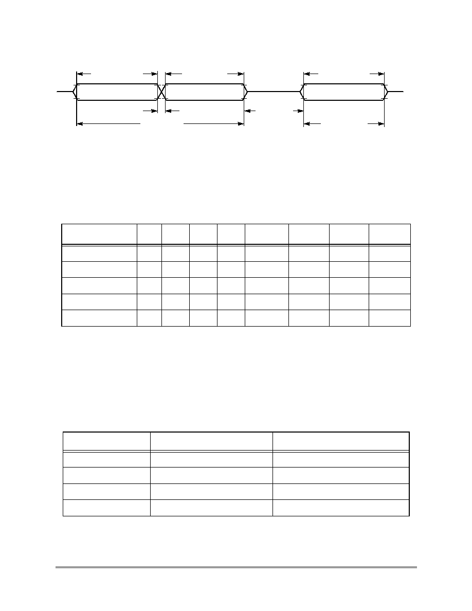
3.4 AC Electrical Characteristics
Timing waveforms in
Section 3.4
are tested using the V
IL
and V
IH
levels specified in the DC Characteristics
table. In
Figure 6
the levels of V
IH
and V
IL
for an input signal are shown.
Figure 6. Input Signal Measurement References
Figure 7
shows the definitions of the following signal states:
·
Active state, when a bus or signal is driven, and enters a low impedance state.
·
Tri-stated, when a bus or signal is placed in a high impedance state.
·
Data Valid state, when a signal level has reached V
OL
or V
OH.
·
Data Invalid state, when a signal level is in transition between V
OL
and V
OH.
3.3V
Regulator
2.5V
Regulator
Supply
V
DD
V
DDIO,
V
DDA
V
IH
V
IL
Fall Time
Input Signal
Note: The midpoint is V
IL
+ (V
IH
V
IL
)/2.
Midpoint1
Low
High
Pulse Width
90%
50%
10%
Rise Time
22
56F826 Technical Data
MOTOROLA
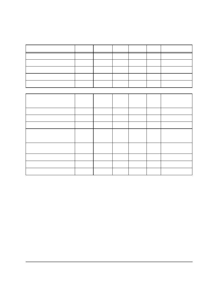
3.5 Flash Memory Characteristics
Figure 7. Signal States
Table 8. Flash Memory Truth Table
Mode
XE
1
1.
X address enable, all rows are disabled when XE = 0
YE
2
2.
Y address enable, YMUX is disabled when YE = 0
SE
3
3. Sense
amplifier
enable
OE
4
4.
Output enable, tri-state Flash data out bus when OE = 0
PROG
5
5. Defines
program
cycle
ERASE
6
6. Defines
erase
cycle
MAS1
7
7.
Defines mass erase cycle, erase whole block
NVSTR
8
8.
Defines non-volatile store cycle
Standby
L
L
L
L
L
L
L
L
Read
H
H
H
H
L
L
L
L
Word Program
H
H
L
L
H
L
L
H
Page Erase
H
L
L
L
L
H
L
H
Mass Erase
H
L
L
L
L
H
H
H
Table 9. IFREN Truth Table
Mode
IFREN = 1
IFREN = 0
Read
Read information block
Read main memory block
Word program
Program information block
Program main memory block
Page erase
Erase information block
Erase main memory block
Mass erase
Erase both block
Erase main memory block
Data Invalid State
Data1
Data2 Valid
Data
Tri-stated
Data3 Valid
Data2
Data3
Data1 Valid
Data Active
Data Active
Flash Memory Characteristics
MOTOROLA
56F826 Technical Data
23
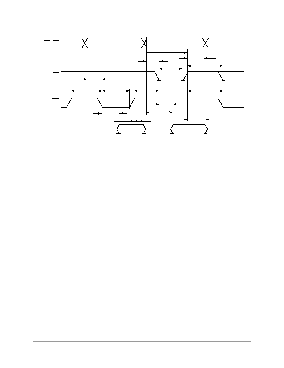
Table 10. Flash Timing Parameters
Operating Conditions:
V
SS
= V
SSA
= 0 V, V
DD
= V
DDA
= 3.03.6V, T
A
= 40
° to +85°C, C
L
50pF
Characteristic
Symbol
Min Typ
Max
Unit
Figure
Program time
T
prog*
20
us
Figure 8
Erase time
T
erase*
20
ms
Figure 9
Mass erase time
T
me*
100
ms
Figure 10
Endurance
1
1.
One cycle is equal to an erase program and read.
E
CYC
10,000
20,000
cycles
Data Retention
1
@ 5000 cycles
D
RET
10
30
years
The following parameters should only be used in the Manual Word Programming Mode
PROG/ERASE to NVSTR set
up time
T
nvs*
5
us
Figure 8
,
Figure 9
,
Figure 10
NVSTR hold time
T
nvh*
5
us
Figure 8
,
Figure 9
NVSTR hold time (mass erase)
T
nvh1*
100
us
Figure 10
NVSTR to program set up time
T
pgs*
10
us
Figure 8
Recovery time
T
rcv*
1
us
Figure 8
,
Figure 9
,
Figure 10
Cumulative program
HV period
2
2.
Thv is the cumulative high voltage programming time to the same row before next erase. The same address cannot
be programmed twice before next erase.
T
hv
3
ms
Figure 8
Program hold time
3
3.
Parameters are guaranteed by design in smart programming mode and must be one cycle or greater.
*The Flash interface unit provides registers for the control of these parameters.
T
pgh
Figure 8
Address/data set up time
3
T
ads
Figure 8
Address/data hold time
3
T
adh
Figure 8
24
56F826 Technical Data
MOTOROLA
Figure 8. Flash Program Cycle
Figure 9. Flash Erase Cycle
XADR
YADR
YE
DIN
PROG
NVSTR
Tnvs
Tpgs
Tadh
Tprog
Tads
Tpgh
Tnvh
Trcv
Thv
IFREN
XE
XADR
YE=SE=OE=MAS1=0
ERASE
NVSTR
Tnvs
Tnvh
Trcv
Terase
IFREN
XE
External Clock Operation
MOTOROLA
56F826 Technical Data
25
Figure 10. Flash Mass Erase Cycle
3.6 External Clock Operation
The 56F826 system clock can be derived from a crystal or an external system clock signal. To generate a
reference frequency using the internal oscillator, a reference crystal must be connected between the EXTAL
and XTAL pins.
3.6.1
Crystal Oscillator
The internal oscillator is also designed to interface with a parallel-resonant crystal resonator in the
frequency range specified for the external crystal in
Table 12
. In
Figure 11
a recommended crystal
oscillator circuit is shown. Follow the crystal supplier's recommendations when selecting a crystal,
because crystal parameters determine the component values required to provide maximum stability and
reliable start-up. The crystal and associated components should be mounted as close as possible to the
EXTAL and XTAL pins to minimize output distortion and start-up stabilization time.The internal 56F82x
oscillator circuitry is designed to have no external load capacitors present. As shown in
Figure 11
no
external load capacitors should be used.
The 56F82x components internally are modeled to provide a capacitive load on each of the oscillator pins
(XTAL and EXATL) of 10pF to 13pF over temperature and process variations. Using a typical value of
internal capacitance on these pins of 12pF and a value of 3pF as a typical circuit board trace capacitance
the parallel load capacitance presented to the crystal is 9pF. This is the value load capacitance that should
be used when selecting a crystal and determining the actual frequency of operation of the crystal oscillator
circuit.
XADR
YE=SE=OE=0
ERASE
NVSTR
Tnvs
Tnvh1
Trcv
Tme
MAS1
IFREN
XE
26
56F826 Technical Data
MOTOROLA
Figure 11. Connecting to a Crystal Oscillator Circuit
3.6.2
Ceramic Resonator
It is also possible to drive the internal oscillator with a ceramic resonator, assuming the overall system
design can tolerate the reduced signal integrity. In
Figure 12
, a typical ceramic resonator circuit is shown.
Refer to supplier's recommendations when selecting a ceramic resonator and associated components. The
resonator and components should be mounted as close as possible to the EXTAL and XTAL pins. The
internal 56F82x oscillator circuitry is designed to have no external load capacitors present. As shown in
Figure 12
no external load capacitors should be used.
Figure 12. Connecting a Ceramic Resonator
Note: Motorola recommends only two terminal ceramic resonators vs. three terminal
resonators (which contain an internal bypass capacitor to ground).
3.6.3
External Clock Source
The recommended method of connecting an external clock is given in
Figure 13
. The external clock
source is connected to XTAL and the EXTAL pin is held V
DDA
/2.
Figure 13. Connecting an External Clock Signal
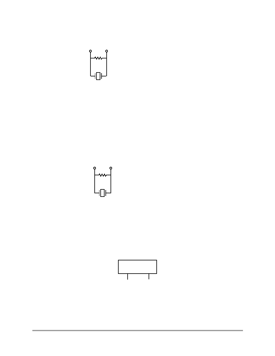
Recommended External Crystal
Parameters:
R
z
= 1 to 3M
f
c
= 4Mhz (optimized for 4MHz)
EXTAL XTAL
R
z
f
c
Recommended Ceramic Resonator
Parameters:
R
z
= 1 to 3 M
f
c
= 4Mhz (optimized for 4MHz)
EXTAL XTAL
R
z
f
c
56F826
XTAL
EXTAL
External
V
DDA
/2
Clock
External Clock Operation
MOTOROLA
56F826 Technical Data
27
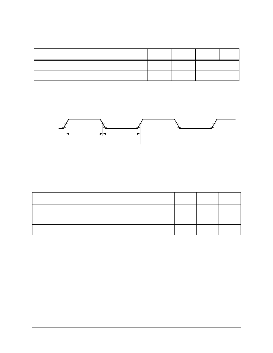
Figure 14. External Clock Timing
3.6.4
Phase Locked Loop Timing
Table 11. External Clock Operation Timing Requirements
Operating Conditions:
V
SSIO
=V
SS
= V
SSA
= 0V, V
DDA
=V
DDIO
=3.03.6V, V
DD
= 2.252.75V, T
A
= 40
° to +85°C, C
L
50pF, f
op
= 80MHz
Characteristic
Symbol
Min
Typ
Max
Unit
Frequency of operation (external clock driver)
1
1. See
Figure 13
for details on using the recommended connection of an external clock driver.
f
osc
0
4
80
2
2.
When using Time of Day (TOD), maximum external frequency is 6MHz.
MHz
Clock Pulse Width
3,
4
3.
The high or low pulse width must be no smaller than 6.25ns or the chip will not function.
4.
Parameters listed are guaranteed by design.
t
PW
6.25
--
--
ns
Table 12. PLL Timing
Operating Conditions:
V
SSIO
=V
SS
= V
SSA
= 0V, V
DDA
=V
DDIO
=3.03.6V, V
DD
= 2.252.75V, T
A
= 40
° to +85°C, C
L
50pF, f
op
= 80MHz
Characteristic
Symbol
Min
Typ
Max
Unit
External reference crystal frequency for the PLL
1
1.
An externally supplied reference clock should be as free as possible from any phase jitter for the PLL to work
correctly. The PLL is optimized for 4MHz input crystal.
f
osc
2
4
6
MHz
PLL output frequency
2
2.
ZCLK may not exceed 80MHz. For additional information on ZCLK and
f
out
/2,
please refer to the OCCS chapter
in the User Manual. ZCLK = f
op
f
out
/2
40
--
110
MHz
PLL stabilization time
3
-40
o
to +85
o
C
3.
This is the minimum time required after the PLL set-up is changed to ensure reliable operation.
t
plls
--
1
10
ms
External
Clock
V
IH
V
IL
Note: The midpoint is V
IL
+ (V
IH
V
IL
)/2.
90%
50%
10%
90%
50%
10%
t
PW
t
PW
28
56F826 Technical Data
MOTOROLA
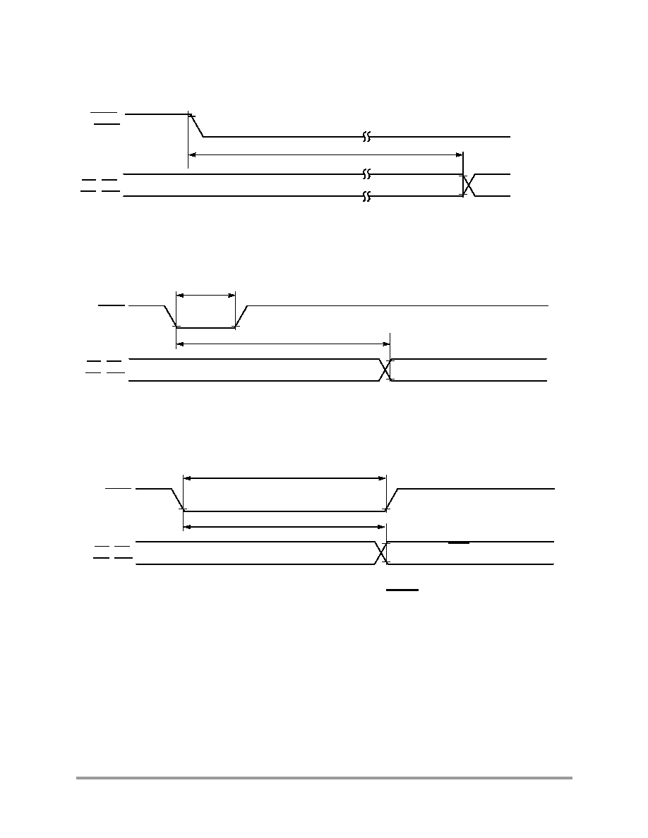
3.7 External Bus Asynchronous Timing
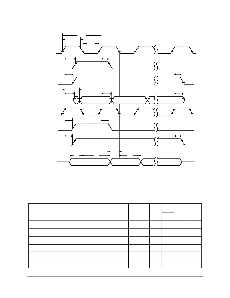
Table 13. External Bus Asynchronous Timing
1, 2
Operating Conditions:
V
SSIO
=V
SS
= V
SSA
= 0V, V
DDA
=V
DDIO
=3.03.6V, V
DD
= 2.252.75V, T
A
= 40
° to +85°C, C
L
50pF, f
op
= 80MHz
1.
Timing is both wait state- and frequency-dependent. In the formulas listed, WS = the number of wait states and
T = Clock Period. For 80MHz operation, T = 12.5ns.
2.
Parameters listed are guaranteed by design.
To calculate the required access time for an external memory for any frequency < 80Mhz, use this formula:
Top = Clock period @ desired operating frequency
WS = Number of wait states
Memory Access Time = (Top*WS) + (Top- 11.5)
Characteristic
Symbol
Min
Max
Unit
Address Valid to WR Asserted
t
AWR
6.5
--
ns
WR Width Asserted
Wait states = 0
Wait states > 0
t
WR
7.5
(T*WS) + 7.5
--
--
ns
ns
WR Asserted to D0D15 Out Valid
t
WRD
--
T + 4.2
ns
Data Out Hold Time from WR Deasserted
t
DOH
4.8
--
ns
Data Out Set Up Time to WR Deasserted
Wait states = 0
Wait states > 0
t
DOS
2.2
(T*WS) + 6.4
--
--
ns
ns
RD Deasserted to Address Not Valid
t
RDA
0
--
ns
Address Valid to RD Deasserted
Wait states = 0
Wait states > 0
t
ARDD
18.7
(T*WS) + 18.7
--
ns
ns
Input Data Hold to RD Deasserted
t
DRD
0
--
ns
RD Assertion Width
Wait states = 0
Wait states > 0
t
RD
19
(T*WS) + 19
--
--
ns
ns
Address Valid to Input Data Valid
Wait states = 0
Wait states > 0
t
AD
--
--
1
(T*WS) + 1
ns
ns
Address Valid to RD Asserted
t
ARDA
-4.4
--
ns
RD Asserted to Input Data Valid
Wait states = 0
Wait states > 0
t
RDD
--
--
2.4
(T*WS) + 2.4
ns
ns
WR Deasserted to RD Asserted
t
WRRD
6.8
--
ns
RD Deasserted to RD Asserted
t
RDRD
0
--
ns
WR Deasserted to WR Asserted
t
WRWR
14.1
--
ns
RD Deasserted to WR Asserted
t
RDWR
12.8
--
ns
External Bus Asynchronous Timing
MOTOROLA
56F826 Technical Data
29
Figure 15. External Bus Asynchronous Timing
A0A15,
PS, DS
(See Note)
WR
D0D15
RD
Note: During read-modify-write instructions and internal instructions, the address lines do not change state.
Data In
Data Out
t
AWR
t
ARDA
t
ARDD
t
RDA
t
RD
t
RDRD
t
RDWR
t
WRWR
t
WR
t
DOS
t
WRD
t
WRRD
t
AD
t
DOH
t
DRD
t
RDD
30
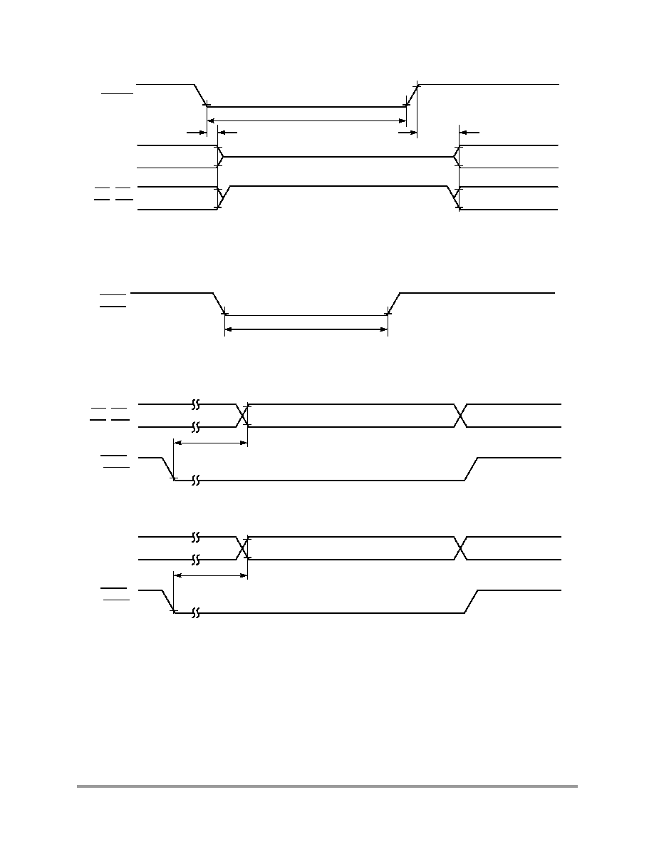
56F826 Technical Data
MOTOROLA
3.8 Reset, Stop, Wait, Mode Select, and Interrupt Timing
Table 14. Reset, Stop, Wait, Mode Select, and Interrupt Timing
1, 5
Operating Conditions:
V
SSIO
=V
SS
= V
SSA
= 0V, V
DDA
=V
DDIO
=3.03.6V, V
DD
= 2.252.75V, T
A
= 40
° to +85°C, C
L
50pF, f
op
= 80MHz
1.
In the formulas, T = clock cycle. For an operating frequency of 80MHz, T = 12.5ns.
Characteristic
Symbol
Min
Max
Unit
See
Figure
RESET Assertion to Address, Data and Control
Signals High Impedance
t
RAZ
--
21
ns
Figure 16
Minimum RESET Assertion Duration
2
OMR Bit 6 = 0
OMR Bit 6 = 1
2.
Circuit stabilization delay is required during reset when using an external clock or crystal oscillator in two cases:
· After power-on reset
· When recovering from Stop state
t
RA
275,000T
128T
--
--
ns
ns
Figure 16
RESET Deassertion to First External Address Output
t
RDA
33T
34T
ns
Figure 16
Edge-sensitive Interrupt Request Width
t
IRW
1.5T
--
ns
Figure 17
IRQA, IRQB Assertion to External Data Memory
Access Out Valid, caused by first instruction execution
in the interrupt service routine
t
IDM
--
15T
ns
Figure 18
IRQA, IRQB Assertion to General Purpose Output
Valid, caused by first instruction execution in the
interrupt service routine
t
IG
--
16T
ns
Figure 18
IRQA Low to First Valid Interrupt Vector Address Out
recovery from Wait State
3
3.
The minimum is specified for the duration of an edge-sensitive IRQA interrupt required to recover from the Stop state.
This is not the minimum required so that the IRQA interrupt is accepted.
t
IRI
--
13T
ns
Figure 19
IRQA Width Assertion to Recover from Stop State
4
4.
The interrupt instruction fetch is visible on the pins only in Mode 3.
5.
Parameters listed are guaranteed by design.
t
IW
--
2T
ns
Figure 20
Delay from IRQA Assertion to Fetch of first instruction
(exiting Stop)
OMR Bit 6 = 0
OMR Bit 6 = 1
t
IF
--
--
275,000T
12T
ns
ns
Figure 20
Duration for Level Sensitive IRQA Assertion to Cause
the Fetch of First IRQA Interrupt Instruction (exiting
Stop)
OMR Bit 6 = 0
OMR Bit 6 = 1
t
IRQ
--
--
275,000T
12T
ns
ns
Figure 21
Delay from Level Sensitive IRQA Assertion to First
Interrupt Vector Address Out Valid (exiting Stop)
OMR Bit 6 = 0
OMR Bit 6 = 1
t
II
--
--
275,000T
12T
ns
ns
Figure 21
Reset, Stop, Wait, Mode Select, and Interrupt Timing
MOTOROLA
56F826 Technical Data
31
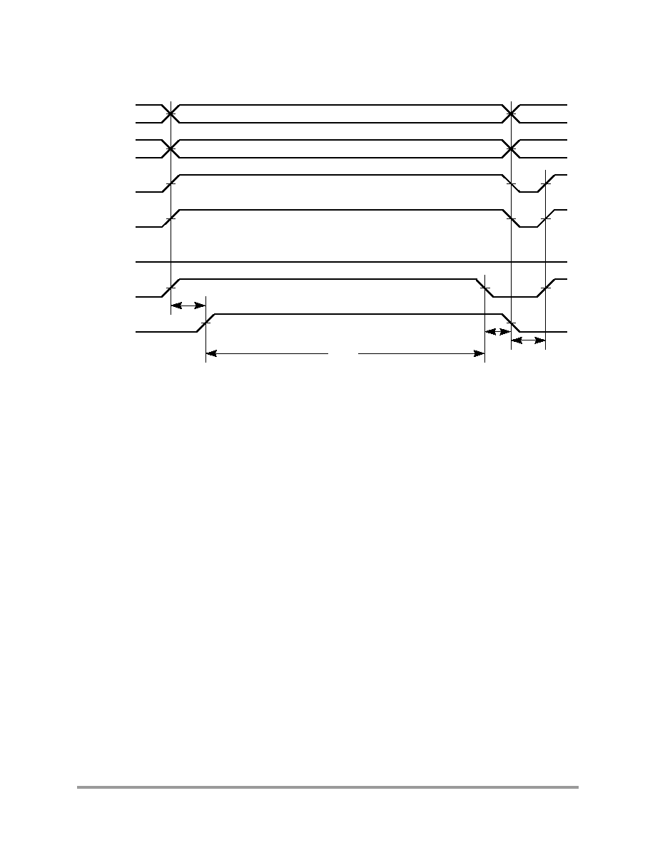
Figure 16. Asynchronous Reset Timing
Figure 17. External Interrupt Timing (Negative-Edge-Sensitive)
Figure 18. External Level-Sensitive Interrupt Timing
First Fetch
A0A15,
D0D15
PS, DS,
RD, WR
RESET
First Fetch
t
RA
t
RAZ
t
RDA
IRQA,
IRQB
t
IRW
A0A15,
PS, DS,
RD, WR
IRQA,
IRQB
First Interrupt Instruction Execution
a) First Interrupt Instruction Execution
General
Purpose
I/O Pin
IRQA,
IRQB
b) General Purpose I/O
t
IDM
t
IG
32
56F826 Technical Data
MOTOROLA
Figure 19. Interrupt from Wait State Timing
Figure 20. Recovery from Stop State Using Asynchronous Interrupt Timing
Figure 21. Recovery from Stop State Using IRQA Interrupt Service
Instruction Fetch
IRQA,
IRQB
First Interrupt Vector
A0A15,
PS, DS,
RD, WR
t
IRI
Not IRQA Interrupt Vector
IRQA
A0A15,
PS, DS,
RD, WR
First Instruction Fetch
t
IW
t
IF
Instruction Fetch
IRQA
A0A15
PS, DS,
RD, WR
First IRQA Interrupt
t
IRQ
t
II
Serial Peripheral Interface (SPI) Timing
MOTOROLA
56F826 Technical Data
33
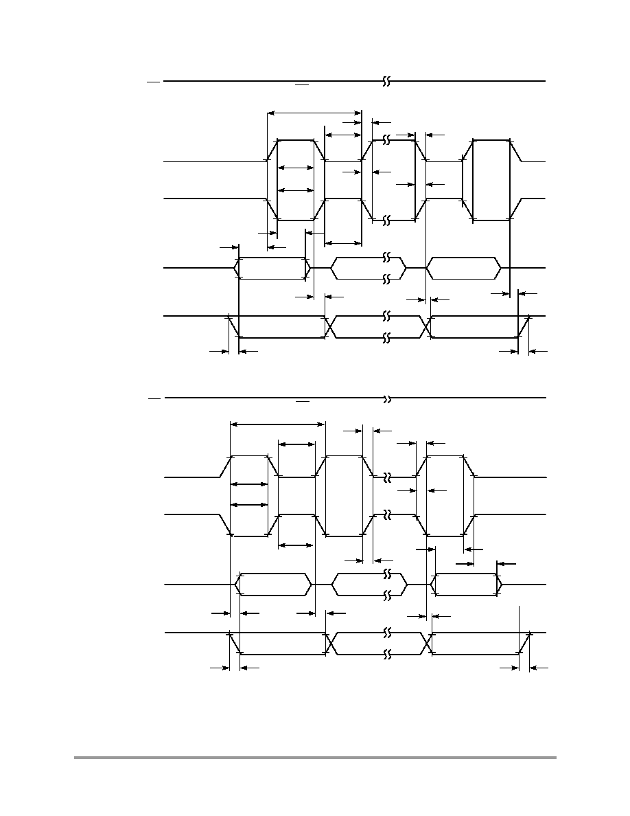
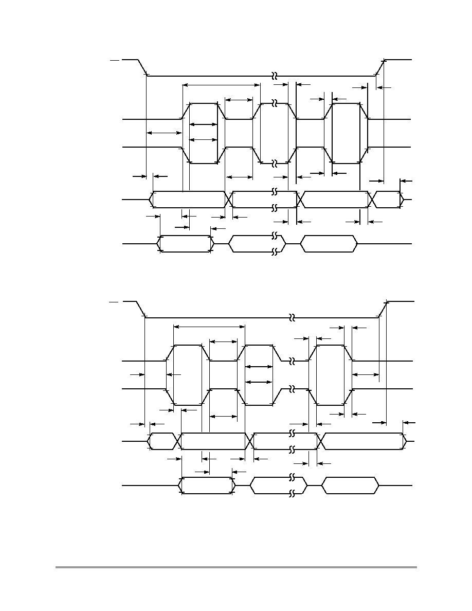
3.9 Serial Peripheral Interface (SPI) Timing
1.Parameters listed are guaranteed by design.
Table 15. SPI Timing
1
Operating Conditions:
V
SSIO
=V
SS
= V
SSA
= 0V, V
DDA
=V
DDIO
=3.03.6V, V
DD
= 2.252.75V, T
A
= 40
° to +85°C, C
L
50pF, f
op
= 80MHz
Characteristic
Symbol
Min
Max
Unit
See Figure
Cycle time
Master
Slave
t
C
50
25
--
--
ns
ns
Figures
22
,
23
,
24
,
25
Enable lead time
Master
Slave
t
ELD
--
25
--
--
ns
ns
Figure
25
Enable lag time
Master
Slave
t
ELG
--
100
--
--
ns
ns
Figure
25
Clock (SCLK) high time
Master
Slave
t
CH
24
12
--
--
ns
ns
Figures
22
,
23
,
24
,
25
Clock (SCLK) low time
Master
Slave
t
CL
24.1
12
--
--
ns
ns
Figures
22
,
23
,
24
,
25
Data set-up time required for inputs
Master
Slave
t
DS
20
0
--
--
ns
ns
Figures
22
,
23
,
24
,
25
Data hold time required for inputs
Master
Slave
t
DH
0
2
--
--
ns
ns
Figures
22
,
23
,
24
,
25
Access time (time to data active from high-impedance state)
Slave
t
A
4.8
15
ns
Figure
25
Disable time (hold time to high-impedance state)
Slave
t
D
3.7
15.2
ns
Figure
25
Data Valid for outputs
Master
Slave (after enable edge)
t
DV
--
--
4.5
20.4
ns
ns
Figures
22
,
23
,
24
,
25
Data invalid
Master
Slave
t
DI
0
0
--
--
ns
ns
Figures
22
,
23
,
24
,
25
Rise time
Master
Slave
t
R
--
--
11.5
10.0
ns
ns
Figures
22
,
23
,
24
,
25
Fall time
Master
Slave
t
F
--
--
9.7
9.0
ns
ns
Figures
22
,
23
,
24
,
25
34
56F826 Technical Data
MOTOROLA
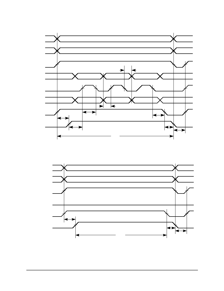
Figure 22. SPI Master Timing (CPHA = 0)
Figure 23. SPI Master Timing (CPHA = 1)
SCLK (CPOL = 0)
(Output)
SCLK (CPOL = 1)
(Output)
MISO
(Input)
MOSI
(Output)
MSB in
Bits 141
LSB in
Master MSB out
Bits 141
Master LSB out
SS
(Input)
SS is held High on master
t
R
t
F
t
F
t
DI
t
DS
t
DI
(ref)
t
DV
t
CH
t
DH
t
C
t
R
t
F
t
R
t
CL
t
CH
t
CL
SCLK (CPOL = 0)
(Output)
SCLK (CPOL = 1)
(Output)
MISO
(Input)
MOSI
(Output)
MSB in
Bits 141
LSB in
Master MSB out
Bits 14 1
Master LSB out
SS
(Input)
SS is held High on master
t
C
t
CL
t
F
t
DI
t
DV
(ref)
t
DV
t
R
t
DH
t
DS
t
R
t
CH
t
CH
t
CL
t
F
t
R
t
F
Serial Peripheral Interface (SPI) Timing
MOTOROLA
56F826 Technical Data
35
Figure 24. SPI Slave Timing (CPHA = 0)
Figure 25. SPI Slave Timing (CPHA = 1)
SCLK (CPOL = 0)
(Input)
SCLK (CPOL = 1)
(Input)
MISO
(Output)
MOSI
(Input)
Slave MSB out
Bits 141
MSB in
Bits 141
LSB in
SS
(Input)
Slave LSB out
t
ELG
t
F
t
R
t
C
t
CL
t
CH
t
CL
t
ELD
t
A
t
CH
t
R
t
F
t
D
t
DI
t
DI
t
DS
t
DH
t
DV
SCLK (CPOL = 0)
(Input)
SCLK (CPOL = 1)
(Input)
MISO
(Output)
MOSI
(Input)
Slave MSB out
Bits 141
MSB in
Bits 141
LSB in
SS
(Input)
Slave LSB out
t
C
t
CL
t
DV
t
A
t
ELD
t
R
t
F
t
ELG
t
CH
t
CL
t
CH
t
F
t
DS
t
DV
t
DI
t
DH
t
D
t
R
36
56F826 Technical Data
MOTOROLA
3.10 Synchronous Serial Interface (SSI) Timing
Table 16. SSI Master Mode
1
Switching Characteristics
Operating Conditions:
V
SSIO
=V
SS
= V
SSA
= 0V, V
DDA
=V
DDIO
=3.03.6V, V
DD
= 2.252.75V, T
A
= 40
° to +85°C, C
L
50pF, f
op
= 80MHz
1.
Master mode is internally generated clocks and frame syncs
Parameter
Symbol
Min
Typ
Max
Units
STCK frequency
fs
10
2
2.
Max clock frequency is IP_clk/4 = 40MHz / 4 = 10MHz for an 80MHz part.
MHz
STCK period
3
3.
All the timings for the SSI are given for a non-inverted serial clock polarity (TSCKP=0 in SCR2 and RSCKP=0 in
SCSR) and a non-ionverted frame sync (TFSI=0 in SCR2 and RFSI=0 in SCSR). If the polarity of the clock and/or the
frame sync have been inverted, all the timings remain valid by inverting the clock signal STCK/SRCK and/or the frame
sync STFS/SRFS in the tables and in the figures.
t
SCKW
100
--
--
ns
STCK high time
t
SCKH
50
4
4.
50% duty cycle
--
--
ns
STCK low time
t
SCKL
50
4
--
--
ns
Output clock rise/fall time (STCK, SRCK)
--
4
--
ns
Delay from STCK high to STFS (bl) high - Master
5
5.
bl = bit length; wl = word length
t
TFSBHM
0.1
--
0.5
ns
Delay from STCK high to STFS (wl) high - Master
5
t
TFSWHM
0.1
--
0.5
ns
Delay from SRCK high to SRFS (bl) high - Master
5
t
RFSBHM
0.6
--
1.3
ns
Delay from SRCK high to SRFS (wl) high - Master
5
t
RFSWHM
0.6
--
1.3
ns
Delay from STCK high to STFS (bl) low - Master
5
t
TFSBLM
-1.0
--
-0.1
ns
Delay from STCK high to STFS (wl) low - Master
5
t
TFSWLM
-1.0
--
-0.1
ns
Delay from SRCK high to SRFS (bl) low - Master
5
t
RFSBLM
-0.1
--
0
ns
Delay from SRCK high to SRFS (wl) low - Master
5
t
RFSWLM
-0.1
--
0
ns
STCK high to STXD enable from high impedance - Master
t
TXEM
20
--
22
ns
STCK high to STXD valid - Master
t
TXVM
24
--
26
ns
STCK high to STXD not valid - Master
t
TXNVM
0.1
--
0.2
ns
STCK high to STXD high impedance - Master
t
TXHIM
24
--
25.5
ns
SRXD Setup time before SRCK low - Master
t
SM
4
--
--
ns
SRXD Hold time after SRCK low - Master
t
HM
4
--
--
ns
Synchronous Operation (in addition to standard internal clock parameters)
SRXD Setup time before STCK low - Master
t
TSM
4
--
--
SRXD Hold time after STCK low - Master
t
THM
4
--
--
Synchronous Serial Interface (SSI) Timing
MOTOROLA
56F826 Technical Data
37
Figure 26. Master Mode Timing Diagram
Table 17. SSI Slave Mode
1
Switching Characteristics
Operating Conditions: V
SSIO
=V
SS
= V
SSA
= 0V, V
DDA
=V
DDIO
=3.03.6V, V
DD
= 2.252.75V, T
A
= 40
° to +85°C, C
L
50pF, f
op
= 80MHz
Parameter
Symbol
Min
Typ
Max
Units
STCK frequency
fs
--
10
2
MHz
STCK period
3
t
SCKW
100
--
--
ns
STCK high time
t
SCKH
50
4
--
--
ns
STCK low time
t
SCKL
50
4
--
--
ns
Output clock rise/fall time
--
TBD
--
ns
Delay from STCK high to STFS (bl) high - Slave
5
t
TFSBHS
0.1
--
46
ns
Delay from STCK high to STFS (wl) high - Slave
5
t
TFSWHS
0.1
--
46
ns
t
THM
t
TSM
t
HM
t
SM
t
RFSWLM
t
RFSWHM
t
RFBLM
t
RFSBHM
t
TXHIM
t
TXNVM
t
TXVM
t
TXEM
t
TFSWLM
t
TFSWHM
t
TFSBLM
t
TFSBHM
t
SCKL
t
SCKW
t
SCKH
First Bit
Last Bit
STCK output
STFS (bl) output
STFS (wl) output
STXD
SRCK output
SRFS (bl) output
SRFS (wl) output
SRXD
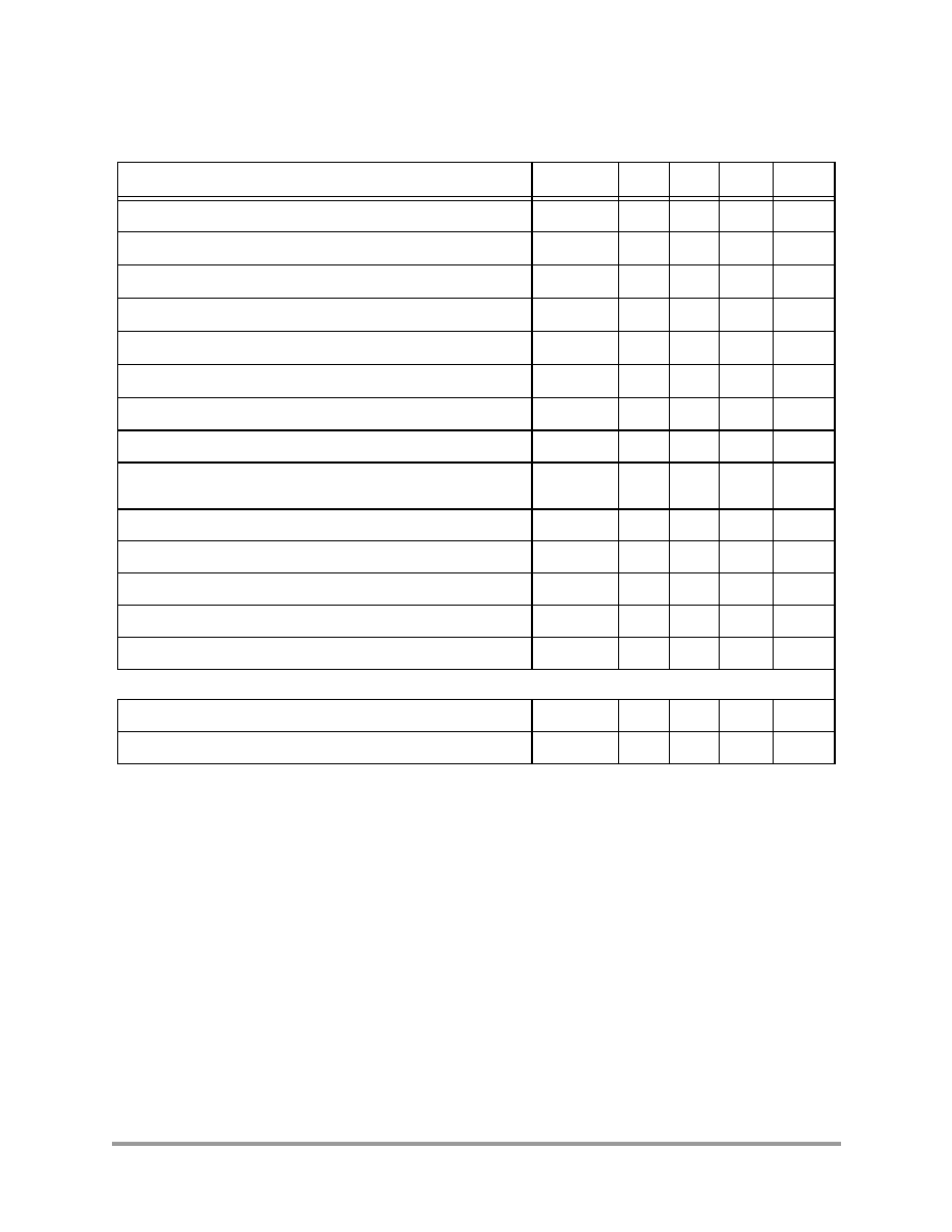
38
56F826 Technical Data
MOTOROLA
Delay from SRCK high to SRFS (bl) high - Slave
5
t
RFSBHS
0.1
--
46
ns
Delay from SRCK high to SRFS (wl) high - Slave
5
t
RFSWHS
0.1
--
46
ns
Delay from STCK high to STFS (bl) low - Slave
5
t
TFSBLS
-1
--
--
ns
Delay from STCK high to STFS (wl) low - Slave
5
t
TFSWLS
-1
--
--
ns
Delay from SRCK high to SRFS (bl) low - Slave
5
t
RFSBLS
-46
--
--
ns
Delay from SRCK high to SRFS (wl) low - Slave
5
t
RFSWLS
-46
--
--
ns
STCK high to STXD enable from high impedance - Slave
t
TXES
--
--
ns
STCK high to STXD valid - Slave
t
TXVS
1
--
25
ns
STFS high to STXD enable from high impedance (first bit) -
Slave
t
FTXES
5.5
--
25
ns
STFS high to STXD valid (first bit) - Slave
t
FTXVS
6
--
27
ns
STCK high to STXD not valid - Slave
t
TXNVS
11
--
13
ns
STCK high to STXD high impedance - Slave
t
TXHIS
11
--
28.5
ns
SRXD Setup time before SRCK low - Slave
t
SS
4
--
--
ns
SRXD Hold time after SRCK low - Slave
t
HS
4
--
--
ns
Synchronous Operation (in addition to standard external clock parameters)
SRXD Setup time before STCK low - Slave
t
TSS
4
--
--
SRXD Hold time after STCK low - Slave
t
THS
4
--
--
1.
Slave mode is externally generated clocks and frame syncs
2.
Max clock frequency is IP_clk/4 = 40MHz / 4 = 10MHz for an 80MHz part.
3.
All the timings for the SSI are given for a non-inverted serial clock polarity (TSCKP=0 in SCR2 and RSCKP=0
in SCSR) and a non-inverted frame sync (TFSI=0 in SCR2 and RFSI=0 in SCSR). If the polarity of the clock and/or the
frame sync have been inverted, all the timings remain valid by inverting the clock signal STCK/SRCK and/or the frame
sync STFS/SRFS in the tables and in the figures.
4. 50%
duty
cycle
5.
bl = bit length; wl = word length
Table 17. SSI Slave Mode
1
Switching Characteristics (Continued)
Operating Conditions: V
SSIO
=V
SS
= V
SSA
= 0V, V
DDA
=V
DDIO
=3.03.6V, V
DD
= 2.252.75V, T
A
= 40
° to +85°C, C
L
50pF, f
op
= 80MHz
Parameter
Symbol
Min
Typ
Max
Units
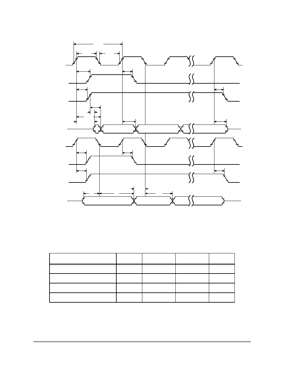
Quad Timer Timing
MOTOROLA
56F826 Technical Data
39
Figure 27. Slave Mode Clock Timing
3.11 Quad Timer Timing
Table 18. Timer Timing
1, 2
Operating Conditions:
V
SSIO
=V
SS
= V
SSA
= 0V, V
DDA
=V
DDIO
=3.03.6V, V
DD
= 2.252.75V, T
A
= 40
° to +85°C, C
L
50pF, f
op
= 80MHz
1.
In the formulas listed, T = clock cycle. For 80MHz operation, T = 12.5ns.
2.
Parameters listed are guaranteed by design.
Characteristic
Symbol
Min
Max
Unit
Timer input period
P
IN
4T+6
--
ns
Timer input high/low period
P
INHL
2T+3
--
ns
Timer output period
P
OUT
2T
--
ns
Timer output high/low period
P
OUTHL
1T
--
ns
t
THS
t
TSS
t
HS
t
SS
t
RFSWLS
t
RFSWHS
t
RFBLS
t
RFSBHS
t
TXHIS
t
TXNVS
t
FTXVS
t
TXVS
t
FTXES
t
TXES
t
TFSWLS
t
TFSWHS
t
TFSBLS
t
TFSBHS
t
SCKL
t
SCKW
t
SCKH
First Bit
Last Bit
STCK input
STFS (bl) input
STFS (wl) input
STXD
SRCK input
SRFS (bl) input
SRFS (wl) input
SRXD
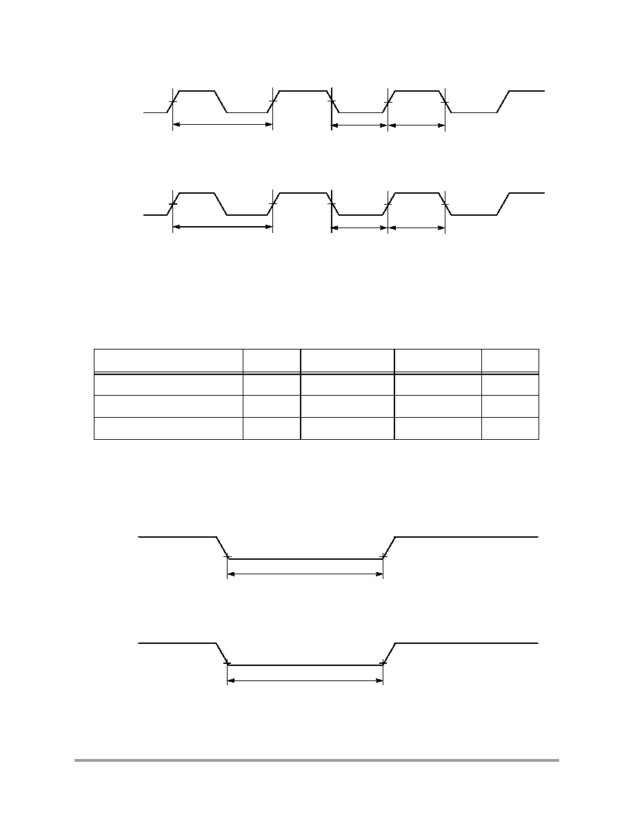
40
56F826 Technical Data
MOTOROLA
3.12 Serial Communication Interface (SCI) Timing
Figure 29. RXD Pulse Width
Figure 30. TXD Pulse Width
Figure 28. Quad Timer Timing
Table 19. SCI Timing
4
Operating Conditions:
V
SSIO
=V
SS
= V
SSA
= 0V, V
DDA
=V
DDIO
=3.03.6V, V
DD
= 2.252.75V, T
A
= 40
° to +85°C, C
L
50pF, f
op
= 80MHz
Characteristic
Symbol
Min
Max
Unit
Baud Rate
1
1. f
MAX
is the frequency of operation of the system clock in MHz.
BR
--
(f
MAX
*2.5)/(80)
Mbps
RXD
2
Pulse Width
2.
The RXD pin in SCI0 is named RXD0 and the RXD pin in SCI1 is named RXD1.
RXD
PW
0.965/BR
1.04/BR
ns
TXD
3
Pulse Width
3.
The TXD pin in SCI0 is named TXD0 and the TXD pin in SCI1 is named TXD1.
4.
Parameters listed are guaranteed by design.
TXD
PW
0.965/BR
1.04/BR
ns
Timer Inputs
Timer Outputs
P
IN
P
INHL
P
INHL
P
OUT
P
OUTHL
P
OUTHL
RXD
SCI receive
data pin
(Input)
RXD
PW
TXD
SCI receive
data pin
(Input)
TXD
PW
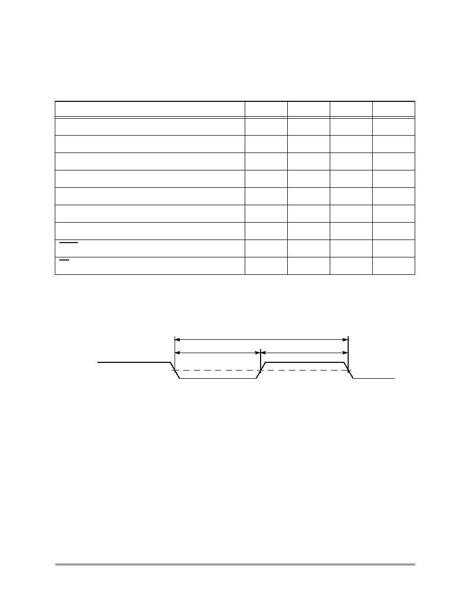
JTAG Timing
MOTOROLA
56F826 Technical Data
41
3.13 JTAG Timing
Table 20. JTAG Timing
1, 3
Operating Conditions:
V
SSIO
=V
SS
= V
SSA
= 0V, V
DDA
=V
DDIO
=3.03.6V, V
DD
= 2.252.75V, T
A
= 40
° to +85°C, C
L
50pF, f
op
= 80MHz
1.
Timing is both wait state and frequency dependent. For the values listed, T = clock cycle. For 80MHz
operation, T = 12.5ns.
Characteristic
Symbol
Min
Max
Unit
TCK frequency of operation
2
2.
TCK frequency of operation must be less than 1/8 the processor rate.
3.
Parameters listed are guaranteed by design.
f
OP
DC
10
MHz
TCK cycle time
t
CY
100
--
ns
TCK clock pulse width
t
PW
50
--
ns
TMS, TDI data set-up time
t
DS
0.4
--
ns
TMS, TDI data hold time
t
DH
1.2
--
ns
TCK low to TDO data valid
t
DV
--
26.6
ns
TCK low to TDO tri-state
t
TS
--
23.5
ns
TRST assertion time
t
TRST
50
--
ns
DE assertion time
t
DE
4T
--
ns
Figure 31. Test Clock Input Timing Diagram
TCK
(Input)
V
M
V
IL
V
M
= V
IL
+ (V
IH
V
IL
)/2
V
M
V
IH
t
PW
t
CY
t
PW
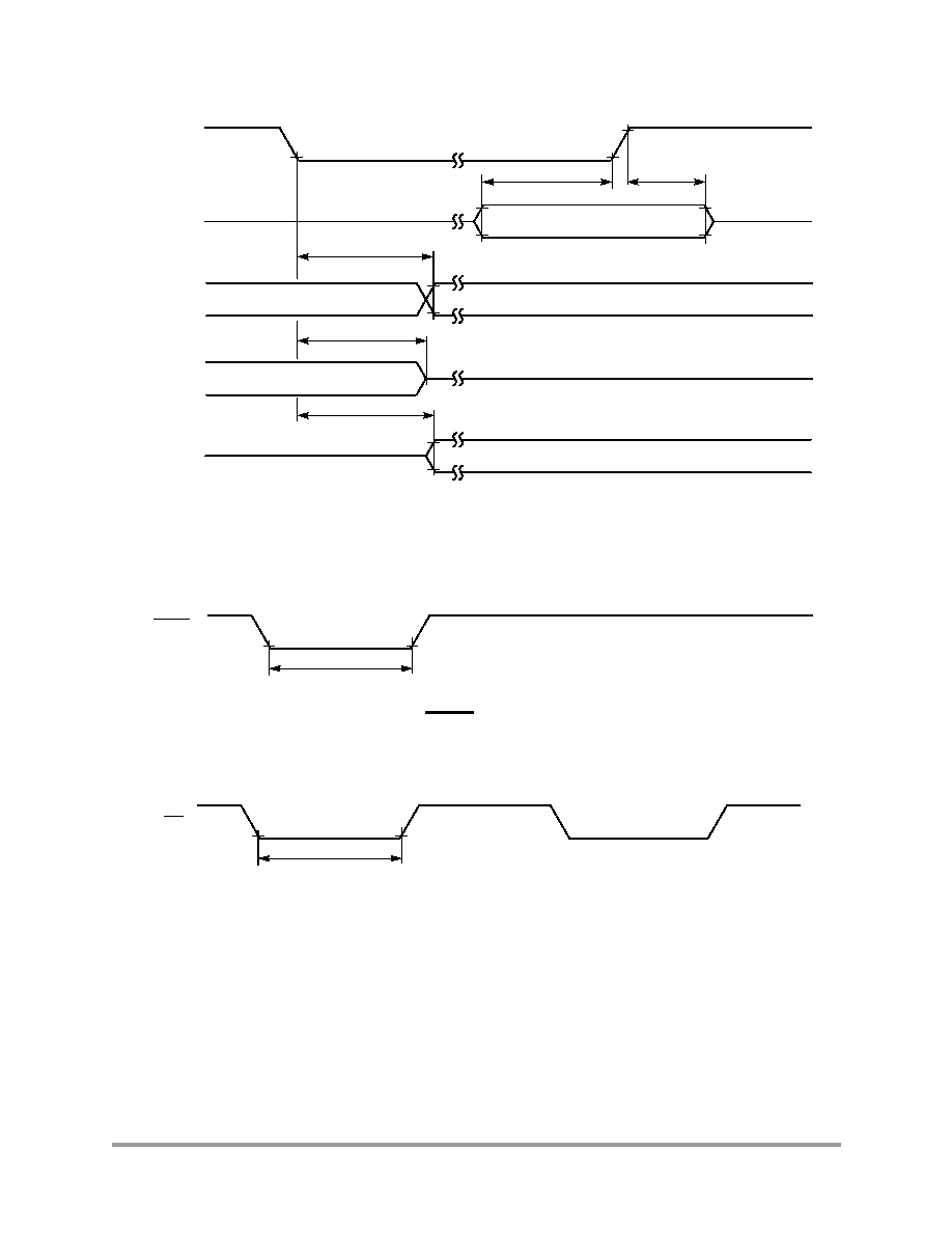
JTAG Timing
MOTOROLA
56F826 Technical Data
42
Figure 32. Test Access Port Timing Diagram
Figure 33. TRST Timing Diagram
Figure 34. OnCE--Debug Event
Input Data Valid
Output Data Valid
Output Data Valid
TCK
(Input)
TDI
(Input)
TDO
(Output)
TDO
(Output
)
TDO
(Output)
TMS
t
DV
t
TS
t
DV
t
DS
t
DH
TRST
(Input)
t
TRST
DE
t
DE
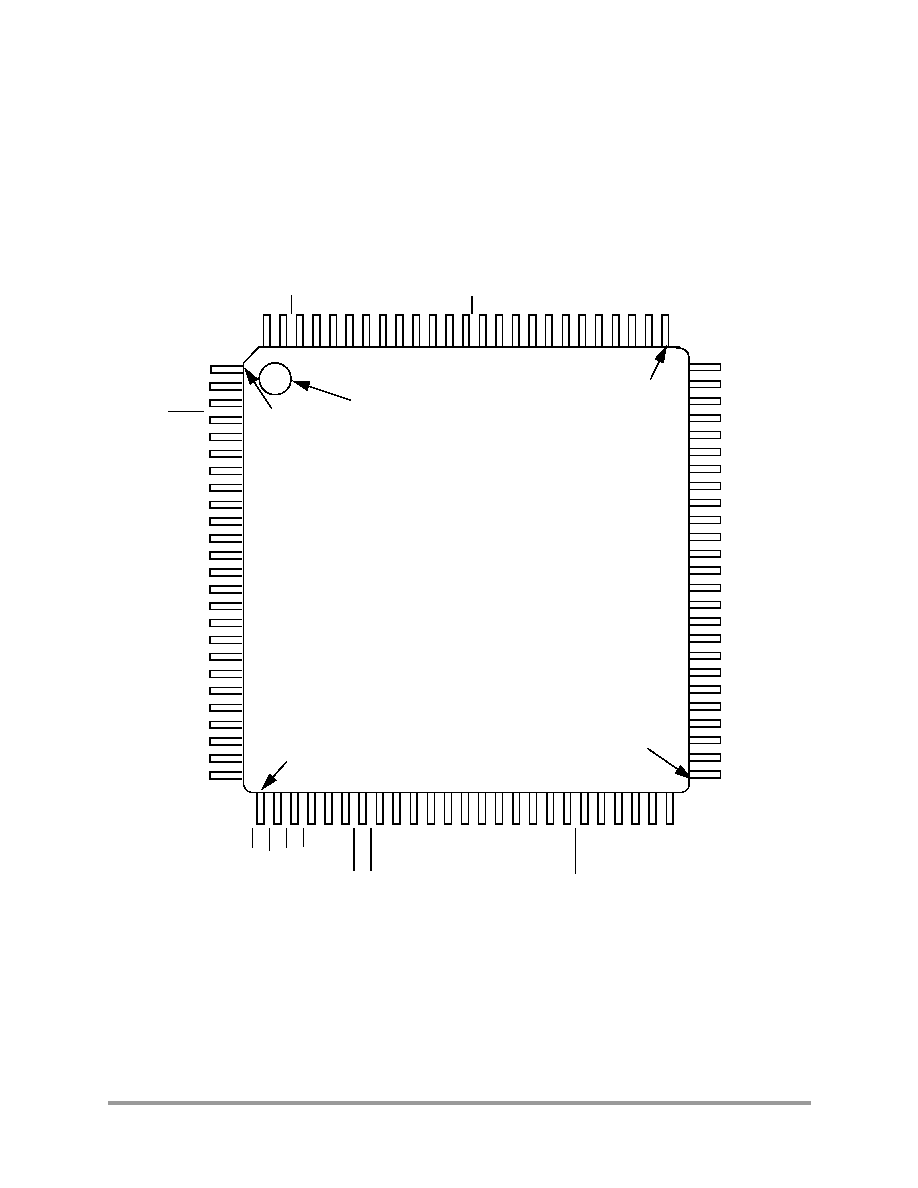
43
56F826 Technical Data
MOTOROLA
Part 4 Packaging
4.1 Package and Pin-Out Information 56F826
This section contains package and pin-out information for the 100-pin LQFP configuration of the 56F826.
Figure 35. Top View, 56F826 100-pin LQFP Package
PIN 1
PIN 26
PIN 51
PIN 76
TMS
TDI
TDO
TRST
VDDIO
VSSIO
A15
A14
A13
A12
A11
A10
A9
A8
A7
A6
A5
A4
VSS
VDD
A3
A2
A1
A0
EXTBOOT
ORIENTATION
MARK
RD
WR
DS
PS
VDDIO
VSSIO
IREQ
A
IREQ
B
D0
D1
D2
D3
D4
D5
D6
D7
D8
D9
D1
0
RESET
D1
1
D1
2
D1
3
D1
4
D1
5
GPIOD1
GPIOD0
GPIOB7
GPIOB6
GPIOB5
GPIOB4
GPIOB3
GPIOB2
GPIOB1
GPIOB0
CLKO
VDD
VSS
XTAL
EXTAL
VSSA
VDDA
VSSIO
VDDIO
STCK
STFS
STD
SRCK
SRFS
SRD
TCK
TCS
DE
TXD0
RXD0
VSS
VDD
TXD1
RXD1
TA
0
TA
1
TA
2
TA
3
SS
MI
S
O
MO
S
I
SCLK
GPI
O
D
7
GPI
O
D
6
VSSIO
VDDIO
GPI
O
D
5
GPI
O
D
4
GPI
O
D
3
GPI
O
D
2
Motorola
56F826
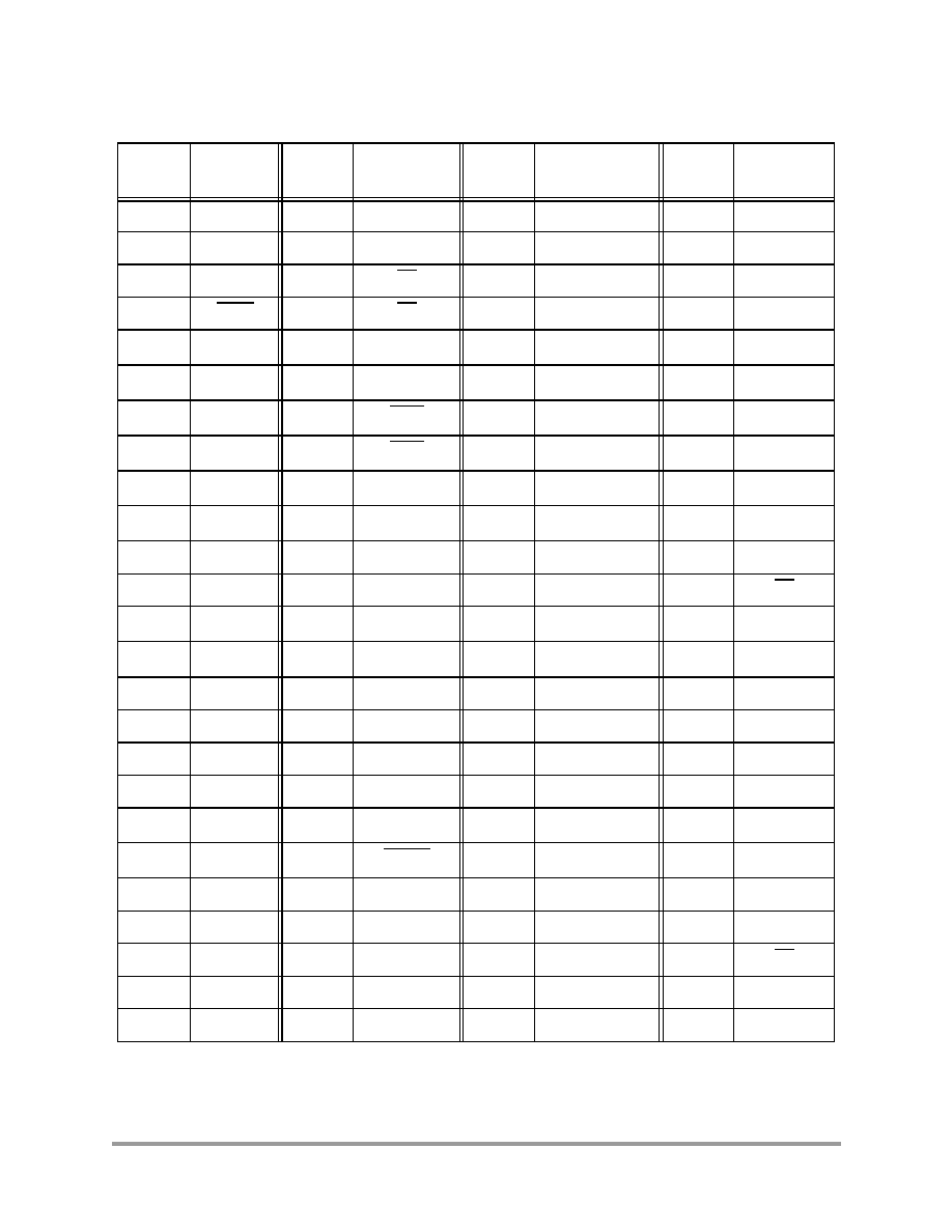
44
56F826 Technical Data
MOTOROLA
Table 21. 56F826 Pin Identification by Pin Number
Pin No.
Signal
Name
Pin No.
Signal Name
Pin No.
Signal Name
Pin No.
Signal
Name
1
TMS
26
RD
51
SRD
76
GPIOD2
2
TDI
27
WR
52
SRFS
77
GPIOD3
3
TDO
28
DS
53
SRCK
78
GPIOD4
4
TRST
29
PS
54
STD
79
GPIOD5
5
V
DDIO
30
V
DDIO
55
STFS
80
V
DDIO
6
V
SSIO
31
V
SSIO
56
STCK
81
V
SSIO
7
A15
32
IRQA
57
V
DDIO
82
GPIOD6
8
A14
33
IRQB
58
V
SSIO
83
GPIOD7
9
A13
34
D0
59
V
DDA
84
SCLK
10
A12
35
D1
60
V
SSA
85
MOSI
11
A11
36
D2
61
EXTAL
86
MISO
12
A10
37
D3
62
XTAL
87
SS
13
A9
38
D4
63
V
SS
88
TA3
14
A8
39
D5
64
V
DD
89
TA2
15
A7
40
D6
65
CLKO
90
TA1
16
A6
41
D7
66
GPIOB0
91
TA0
17
A5
42
D8
67
GPIOB1
92
RXD1
18
A4
43
D9
68
GPIOB2
93
TXD1
19
V
SS
44
D10
69
GPIOB3
94
V
DD
20
V
DD
45
RESET
70
GPIOB4
95
V
SS
21
A3
46
D11
71
GPIOB5
96
RXD0
22
A2
47
D12
72
GPIOB6
97
TXD0
23
A1
48
D13
73
GPIOB7
98
DE
24
A0
49
D14
74
GPIOD0
99
TCS
25
EXTBOOT
50
D15
75
GPIOD1
100
TCK
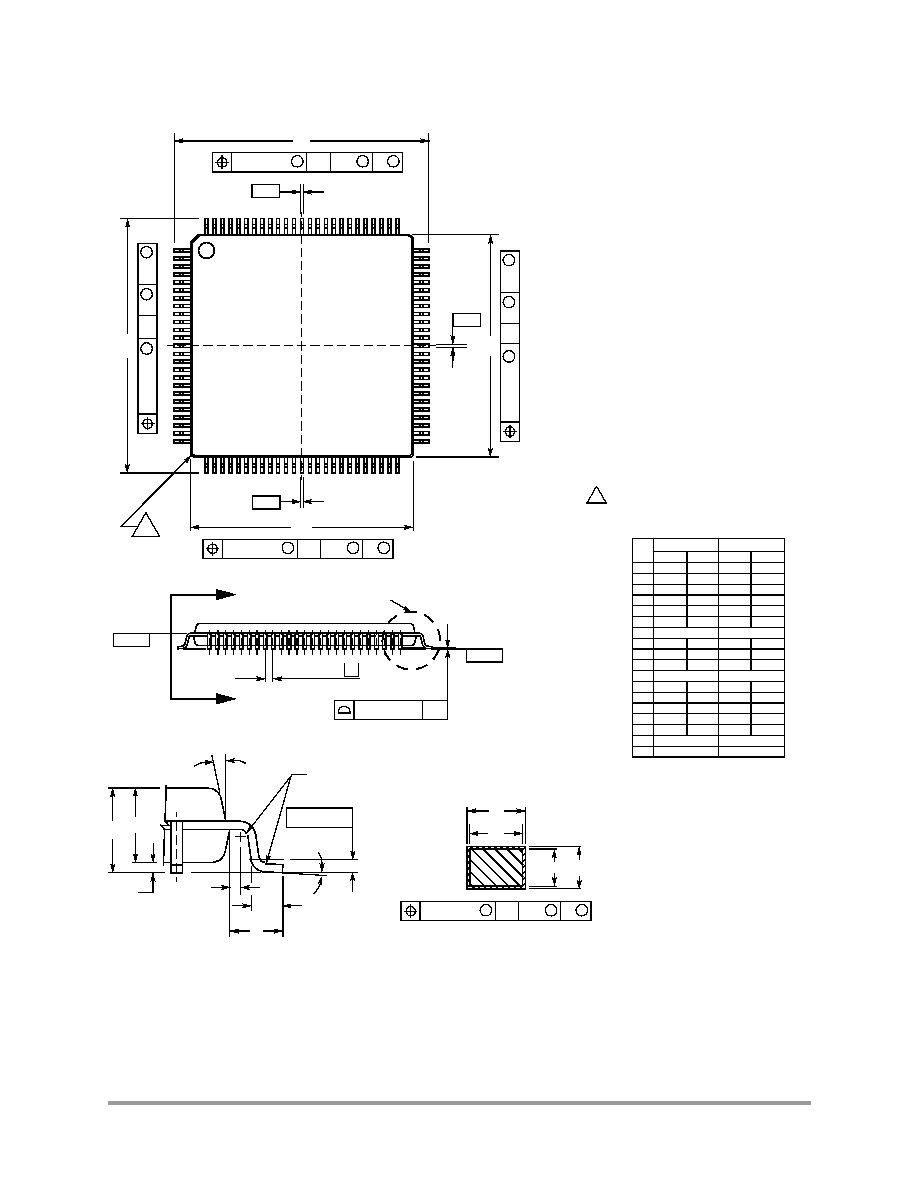
Package and Pin-Out Information 56F826
MOTOROLA
56F826 Technical Data
45
Figure 36. 100-pin LQPF Mechanical Information
NOTES:
1.
DIMENSIONING AND TOLERANCING PER
ANSI Y14.5M, 1982.
2.
CONTROLLING DIMENSION: MILLIMETER.
3.
DATUM PLANE -AB- IS LOCATED AT BOTTOM
OF LEAD AND IS COINCIDENT WITH THE
LEAD WHERE THE LEAD EXITS THE PLASTIC
BODY AT THE BOTTOM OF THE PARTING
LINE.
4.
DATUMS -T-, -U-, AND -Z- TO BE DETERMINED
AT DATUM PLANE -AB-.
5.
DIMENSIONS S AND V TO BE DETERMINED
AT SEATING PLANE -AC-.
6.
DIMENSIONS A AND B DO NOT INCLUDE
MOLD PROTRUSION. ALLOWABLE
PROTRUSION IS 0.250 (0.010) PER SIDE.
DIMENSIONS A AND B DO INCLUDE MOLD
MISMATCH AND ARE DETERMINED AT
DATUM PLANE -AB-.
7.
DIMENSION D DOES NOT INCLUDE DAMBAR
PROTRUSION. DAMBAR PROTRUSION SHALL
NOT CAUSE THE D DIMENSION TO EXCEED
0.350 (0.014). DAMBAR CAN NOT BE LOCATED
ON THE LOWER RADIUS OR THE FOOT.
MINIMUM SPACE BETWEEN PROTRUSION
AND AN ADJACENT LEAD IS 0.070 (0.003).
8.
MINIMUM SOLDER PLATE THICKNESS
SHALL BE 0.0076 (0.003).
9.
EXACT SHAPE OF EACH CORNER MAY VARY
FROM DEPICTION.
AE
AE
AD
SEATING
(24X PER SIDE)
R
GAUGE PLANE
DETAIL AD
SECTION AE-AE
S
V
B
A
96X
X
E
C
K
H
W
D
F
J
N
9
DIM
MIN
MAX
MIN
MAX
INCHES
MILLIMETERS
A 13.950 14.050
0.549
0.553
B
13.950 14.050
0.549
0.553
C
1.400
1.600
0.055
0.063
D
0.170
0.270
0.007
0.011
E
1.350
1.450
0.053
0.057
F
0.170
0.230
0.007
0.009
G
0.500 BSC
0.020 BSC
H
0.050
0.150
0.002
0.006
J
0.090
0.200
0.004
0.008
K
0.500
0.700
0.020
0.028
M
12 REF
12 REF
N
0.090
0.160
0.004
0.006
Q
1
5
1
5
R
0.150
0.250
0.006
0.010
S
15.950 16.050
0.628
0.632
V 15.950 16.050
0.628
0.632
W
0.200 REF
0.008 REF
X
1.000 REF
0.039 REF
°
°
°
°
°
°
CASE 842F-01
-T-
S
T-U
S
0.15(0.006)
Z
S
AC
S
T-
U
S
0.
15
(0.
006
)
Z
S
AC
S
T-
U
S
0.
15
(0.
0
0
6
)
Z
S
AC
-U-
S
T-U
S
0.15(0.006)
Z
S
AB
-Z-
-AC-
G
PLANE
-AB-
S
T-U
M
0.20(0.008)
Z
S
AC
0.100(0.004) AC
Q
°
M
°
0.25 (0.010)

46
56F826 Technical Data
MOTOROLA
Part 5 Design Considerations
5.1 Thermal Design Considerations
An estimation of the chip junction temperature, T
J
, in
°C can be obtained from the equation:
Equation 1:
Where:
T
A
= ambient temperature °C
R
JA
= package junction-to-ambient thermal resistance °C/W
P
D
= power dissipation in package
Historically, thermal resistance has been expressed as the sum of a junction-to-case thermal resistance and
a case-to-ambient thermal resistance:
Equation 2:
Where:
R
JA
= package junction-to-ambient thermal resistance °C/W
R
JC
= package junction-to-case thermal resistance °C/W
R
CA
= package case-to-ambient thermal resistance °C/W
R
JC
is device-related and cannot be influenced by the user. The user controls the thermal environment to
change the case-to-ambient thermal resistance, R
CA
. For example, the user can change the air flow around
the device, add a heat sink, change the mounting arrangement on the Printed Circuit Board (PCB), or
otherwise change the thermal dissipation capability of the area surrounding the device on the PCB. This
model is most useful for ceramic packages with heat sinks; some 90% of the heat flow is dissipated through
the case to the heat sink and out to the ambient environment. For ceramic packages, in situations where the
heat flow is split between a path to the case and an alternate path through the PCB, analysis of the device
thermal performance may need the additional modeling capability of a system level thermal simulation tool.
The thermal performance of plastic packages is more dependent on the temperature of the PCB to which the
package is mounted. Again, if the estimations obtained from R
JA
do not satisfactorily answer whether the
thermal performance is adequate, a system level model may be appropriate.
Definitions:
A complicating factor is the existence of three common definitions for determining the junction-to-case
thermal resistance in plastic packages:
·
Measure the thermal resistance from the junction to the outside surface of the package (case) closest
to the chip mounting area when that surface has a proper heat sink. This is done to minimize
temperature variation across the surface.
·
Measure the thermal resistance from the junction to where the leads are attached to the case. This
definition is approximately equal to a junction to board thermal resistance.
T
J
T
A
P
D
R
JA
×
(
)
+
=
R
JA
R
JC
R
CA
+
=

Electrical Design Considerations
MOTOROLA
56F826 Technical Data
47
·
Use the value obtained by the equation (T
J
T
T
)/P
D
where T
T
is the temperature of the package
case determined by a thermocouple.
The thermal characterization parameter is measured per JESD51-2 specification using a 40-gauge type T
thermocouple epoxied to the top center of the package case. The thermocouple should be positioned so that
the thermocouple junction rests on the package. A small amount of epoxy is placed over the thermocouple
junction and over about 1mm of wire extending from the junction. The thermocouple wire is placed flat
against the package case to avoid measurement errors caused by cooling effects of the thermocouple wire.
When heat sink is used, the junction temperature is determined from a thermocouple inserted at the interface
between the case of the package and the interface material. A clearance slot or hole is normally required in
the heat sink. Minimizing the size of the clearance is important to minimize the change in thermal
performance caused by removing part of the thermal interface to the heat sink. Because of the experimental
difficulties with this technique, many engineers measure the heat sink temperature and then back-calculate
the case temperature using a separate measurement of the thermal resistance of the interface. From this case
temperature, the junction temperature is determined from the junction-to-case thermal resistance.
5.2 Electrical Design Considerations
Use the following list of considerations to assure correct operation:
·
Provide a low-impedance path from the board power supply to each V
DD,
V
DDIO,
and V
DDA
pin on
the hybrid controller, and from the board ground to each V
SS,
V
SSIO,
and V
SSA
(GND) pin.
·
The minimum bypass requirement is to place 0.1
µF capacitors positioned as close as possible to the
package supply pins. The recommended bypass configuration is to place one bypass capacitor on
each of the V
DD
/V
SS
pairs, including V
DDA
/V
SSA
and V
DDIO
/V
SSIO.
Ceramic and tantalum
capacitors tend to provide better performance tolerances.
·
Ensure that capacitor leads and associated printed circuit traces that connect to the chip V
DD,
V
DDIO,
and V
DDA
and V
SS,
V
SSIO,
and V
SSA
(GND) pins are less than 0.5 inch per capacitor lead.
·
Bypass the V
DD
and V
SS
layers of the PCB with approximately 100
µF, preferably with a high-grade
capacitor such as a tantalum capacitor.
·
Because the controller's output signals have fast rise and fall times, PCB trace lengths should be
minimal.
CAUTION
This device contains protective circuitry to guard
against damage due to high static voltage or
electrical fields. However, normal precautions are
advised to avoid application of any voltages higher
than maximum rated voltages to this high-impedance
circuit. Reliability of operation is enhanced if unused
inputs are tied to an appropriate voltage level.
DSP56F826/D
MOTOROLA and the Stylized M Logo are registered in the US Patent & Trademark Office. All other product or service names are the property of their
respective owners. © Motorola, Inc. 2003.
How to reach us:
USA/EUROPE/Locations Not Listed: Motorola Literature Distribution; P.O. Box 5405, Denver, Colorado 80217. 13036752140 or 18004412447
JAPAN: Motorola Japan Ltd.; SPS, Technical Information Center, 3201, MinamiAzabu. Minatoku, Tokyo 1068573 Japan. 81334403569
ASIA/PACIFIC: Motorola Semiconductors H.K. Ltd.; Silicon Harbour Centre, 2 Dai King Street, Tai Po Industrial Estate, Tai Po, N.T., Hong Kong. 85226668334
Technical Information Center: 18005216274
HOME PAGE: http://www.motorola.com/semiconductors/
Motorola reserves the right to make changes without further notice to any products herein. Motorola makes no warranty, representation or guarantee regarding the
suitability of its products for any particular purpose, nor does Motorola assume any liability arising out of the application or use of any product or circuit, and
specifically disclaims any and all liability, including without limitation consequential or incidental damages. "Typical" parameters which may be provided in Motorola
data sheets and/or specifications can and do vary in different applications and actual performance may vary over time. All operating parameters, including
"Typicals" must be validated for each customer application by customer's technical experts. Motorola does not convey any license under its patent rights nor the
rights of others. Motorola products are not designed, intended, or authorized for use as components in systems intended for surgical implant into the body, or other
applications intended to support or sustain life, or for any other application in which the failure of the Motorola product could create a situation where personal injury
or death may occur. Should Buyer purchase or use Motorola products for any such unintended or unauthorized application, Buyer shall indemnify and hold Motorola
and its officers, employees, subsidiaries, affiliates, and distributors harmless against all claims, costs, damages, and expenses, and reasonable attorney fees
arising out of, directly or indirectly, any claim of personal injury or death associated with such unintended or unauthorized use, even if such claim alleges that
Motorola was negligent regarding the design or manufacture of the part. Motorola and the Stylized M Logo are registered trademarks of Motorola, Inc. Motorola,
Inc. is an Equal Opportunity/Affirmative Action Employer.
·
Consider all device loads as well as parasitic capacitance due to PCB traces when calculating
capacitance. This is especially critical in systems with higher capacitive loads that could create
higher transient currents in the V
DD
and V
SS
circuits.
·
Take special care to minimize noise levels on the VREF, V
DDA
and V
SSA
pins.
·
When using Wired-OR mode on the SPI or the IRQx pins, the user must provide an external pull-
up device.
·
Designs that utilize the TRST pin for JTAG port or OnCE module functionality (such as
development or debugging systems) should allow a means to assert TRST whenever RESET is
asserted, as well as a means to assert TRST independently of RESET. TRST must be asserted at
power up for proper operation. Designs that do not require debugging functionality, such as
consumer products, TRST should be tied low.
·
Because the Flash memory is programmed through the JTAG/OnCE port, designers should provide
an interface to this port to allow in-circuit Flash programming.
Part 6 Ordering Information
Table 22
lists the pertinent information needed to place an order. Consult a Motorola Semiconductor sales
office or authorized distributor to determine availability and to order parts.
Table 22. 56F826 Ordering Information
Part
Supply
Voltage
Package Type
Pin
Count
Frequency
(MHz)
Order Number
56F826
3.03.6 V
2.25-2.75 V
Plastic Quad Flat Pack (LQFP)
100
80
DSP56F826BU80
Document Outline