 | –≠–ª–µ–∫—Ç—Ä–æ–Ω–Ω—ã–π –∫–æ–º–ø–æ–Ω–µ–Ω—Ç: UAA1041B | –°–∫–∞—á–∞—Ç—å:  PDF PDF  ZIP ZIP |

Device
Operating
Temperature Range
Package
UAA1041B
SEMICONDUCTOR
TECHNICAL DATA
AUTOMOTIVE DIRECTION
INDICATOR
ORDERING INFORMATION
UAA1041BD
UAA1041B
TA = ≠ 40
∞
to +100
∞
C
SO≠8
Plastic DIP
PIN CONNECTIONS
Order this document by UAA1041B/D
D SUFFIX
PLASTIC PACKAGE
CASE 751
(SO≠8)
NO SUFFIX
PLASTIC PACKAGE
CASE 626
8
1
8
1
Fault Det
Fault Det On/Off
(Top View)
≠VCC
RLY Out
Oscillator
+Vbat
1
2
3
4
8
7
6
5
Start
Oscillator
1
MOTOROLA ANALOG IC DEVICE DATA
Automotive Direction
Indicator
This device was designed for use in conjunction with a relay in automotive
applications. It is also applicable for other warning lamps such as "handbrake
ON," etc.
∑
Defective Lamp Detection
∑
Overvoltage Protection
∑
Short Circuit Detection and Relay Shutdown to Prevent Risk of Fire
∑
Reverse Battery Connection Protection
∑
Integrated Suppression Clamp Diode
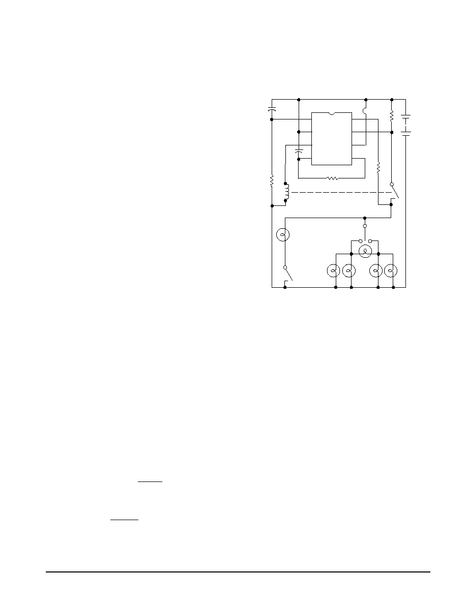
Figure 1. Typical Automotive System
C2
R3
S2
L1
Relay
R1
R2
1
2
3
4
8
7
6
5
C1
+
S1
L
R
L4
L5
L3
L2
L6
+V
≠V
RS
UAA1041
L1: 1.2 W, warning light handbrake ON
L2, L3, L4, L5: 21 W, turn signals
R1 = 75 k
R2 = 3.3 k
R3 = 220
RS = 30 m
C1 = 5.6
µ
F
C2 = 0.047
µ
F
≠VCC
©
Motorola, Inc. 1996
Rev 0

UAA1041B
2
MOTOROLA ANALOG IC DEVICE DATA
MAXIMUM RATINGS
Rating
Pin
Value
Unit
Current: Continuous/Pulse*
1
2
3
8
+150/+500
≠35/≠500
±
350/1900
±
300/1400
±
25/50
mA
Junction Temperature
TJ
150
∞
C
Operating Ambient Temperature Range
TA
≠40 to + 100
∞
C
Storage Temperature Range
Tstg
≠65 to + 150
∞
C
Thermal Resistance, Junction≠to≠Ambient
R
JA
100
∞
C/W (Typ)
* One pulse with an exponential decay and with a time constant of 500 ms.
ELECTRICAL CHARACTERISTICS
(T1 = 25
∞
C)
Characteristics
Symbol
Min
Typ
Max
Unit
Battery Voltage Range (normal operation)
VB
8.0
≠
18
V
Overvoltage Detector Threshold
(VPin2≠VPin1)
Dth(OV)
19
20.2
21.5
V
Clamping Voltage
(VPin2≠VPin1)
VIK
29
31.5
34
V
Short Circuit Detector Threshold
(VPin2≠VPin7)
Dth(SC)
0.63
0.7
0.77
V
Output Voltage (Irelay = ≠250 mA)
(VPin2≠VPin3)
VO
≠
≠
1.5
V
Starter Resistance Rst = R2 + RLamp
Rst
≠
≠
3.6
k
{
Oscillator Constant (normal operation)
Kn
1.4
1.5
1.6
≠
Temperature Coefficient of Kn
Kn
≠
≠1.5x10≠3
≠
1/
∞
C
Duty Cycle (normal operation)
≠
45
50
55
%
Oscillator Constant ≠ (1 lamp defect of 21 W)
KF
0.63
0.68
0.73
≠
Duty Cycle (1 lamp defect of 21 W)
≠
35
40
45
%
Oscillator Constant
K1
K2
K3
0.167
0.25
0.126
0.18
0.27
0.13
0.193
0.29
0.14
≠
Current Consumption (relay off)
Pin 1; at VPin2 ≠ VPin1 = 8.0 V
Pin 1; at VPin2 ≠ VPin1
= 13.5 V
Pin 1; at VPin2 ≠ VPin1
= 18 V
ICC
≠
≠2.5
≠
≠0.9
≠1.6
≠2.2
≠
≠1.0
≠
mA
Current Consumption (relay on)
Pin 1; at VPin2 ≠ VPin1 = 8.0 V
Pin 1; at VPin2 ≠ VPin1
= 13.5 V
Pin 1; at VPin2 ≠ VPin1
= 18 V
≠
≠
≠
≠
≠3.8
≠5.6
≠6.9
≠
≠
≠
mA
Defect Lamp Detector Threshold at VPin2 to VB = 8.0 V
and R3 = 220
= 13.5 V
= 18 V
VPin2≠VPin7
VPin2≠VPin7
VPin2≠VPin7
≠
79
≠
68
85.3
100
≠
91
≠
mV
{
See Note 1 of Application Information
UAA1041B
3
MOTOROLA ANALOG IC DEVICE DATA
CIRCUIT DESCRIPTION
The circuit is designed to drive the direction indicator
flasher relay. Figure 2 shows the typical system configuration
with the external components. It consists of a network (R1,
C1) to determine the oscillator frequency, shunt resistor (RS)
to detect defective bulbs and short circuits in the system, and
two current limiting resistors (R2/R3) to protect the IC against
load dump transients. The circuit can be used either with or
without short circuit detection, and features overvoltage,
defective lamp and short circuit detection.
The lightbulbs L2, L3, L4, L5 are the turn signal indicators
with the dashboard≠light L6. When switch S1 is closed, after
a time delay of t1 (in our example t1 = 75 ms), the relay will be
actuated. The corresponding lightbulbs (L2, L3 or L4, L5) will
flash at the oscillator frequency, independent of the battery
voltage of 8.0 V to 18 V. The flashing cycle stops and the
circuit is reset to the initial position when switch S1 is open.
Overvoltage Detection
Senses the battery voltage. When this voltage exceeds
20.2 V (this is the case when two batteries are connected in
series), the relay will be turned off to protect the lightbulbs.
Lightbulb Defect Detector
Senses the current through the shunt resistor RS. When one
of the lightbulbs is defective, the failure is indicated by
doubling the flashing frequency.
Short Circuit Detector
Detects excessive current (Ish > 25 A) flowing in the shunt
resistor RS. The detection takes place after a time delay of t3
(t3 = 55 ms). In this case, the relay will be turned off. The
circuit is reset by switching S1 to the off position.
Operation with Short Circuit Detection
Pin 6 has to be left open and a capacitor C2 has to be
connected between Pin 1 and Pin 2.
Operation without Short Circuit Detection
Pin 6 has to be connected to Pin 2, and the use of capacitor
C2 is not necessary. The circuit can also be used for other
warning flashers. In this example, when the handbrake is
engaged, it is signaled by the light (L1).
Figure 2. Typical System Configuration
C2
R3
S2
L1
Relay
R1
R2
1
2
3
4
8
7
6
5
C1
+
S1
L
R
L4
L5
L3
L2
L6
+V
≠V
RS
UAA1041B
≠VCC
JU≠1
PARTS LIST
R1 = 75 k
Relay≠Coil Resistance
R2 = 3.3 k
Range 60
to 800
R3 = 220
RS = 30 m
Note: Per text connect
Wire Resistor
jumper JU≠1 bypass
C1 = 5.6
µ
F
short circuit detector
C2 = 0.047
µ
F
C2 may be deleted also.
1. The flashing cycle is started by closing S1. The switch
position is sensed across resistor R2 and RLamp by Input 8.
Rst = R2 + RLamp.
The condition for the start is: Rst < 3.6 k
.
For correct operation, leakage resistance from Pin 8 to
ground must be greater than 5.6 k
.
Flashing frequency: fn =
1
R1C1Kn
2.
Flashing frequency in the case of one defective lightbulb
of 21 W:
3.
fF =
1
R1C1KF
Kn = 2,2KF
t1: delay at the moment when S1 is closed and first flash
t1:
t1 = K1R1C
t2: defective lightbulb detection delay t2 = K2R1C1
t3: short circuit detection delay t3 = K1R1C1
In the case of short circuit ≠ it is assumed that the voltage
(VPin2≠VPin1)
8.0 V. The relay will be turned off after delay
t3. The circuit is reset by switching S1 to the off position.
The capacitor C2 is not obligatory when the short circuit
detector is not used. In this case Pin 6 has to be connected
to Pin 2.
When overvoltage is sensed (VPin2 ≠ VPin1) the relay is
turned off to protect the relay and the lightbulbs against
excessive currents.
4.
5.
6.
7.
8.
APPLICATION INFORMATION
UAA1041B
4
MOTOROLA ANALOG IC DEVICE DATA
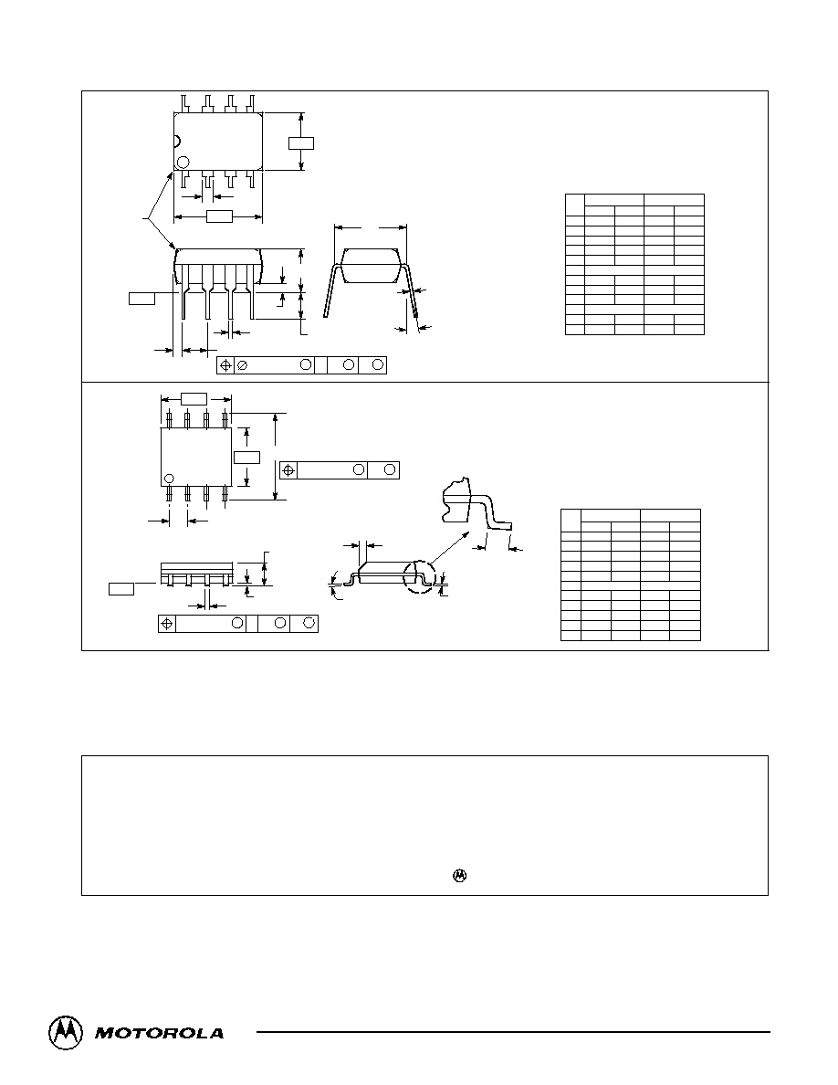
PLASTIC PACKAGE
CASE 626≠05
ISSUE K
D SUFFIX
PLASTIC PACKAGE
CASE 751≠05
(SO≠8)
ISSUE N
OUTLINE DIMENSIONS
1
4
5
8
F
NOTE 2
≠A≠
≠B≠
≠T≠
SEATING
PLANE
H
J
G
D
K
N
C
L
M
M
A
M
0.13 (0.005)
B
M
T
NOTES:
1. DIMENSION L TO CENTER OF LEAD WHEN
FORMED PARALLEL.
2. PACKAGE CONTOUR OPTIONAL (ROUND OR
SQUARE CORNERS).
3. DIMENSIONING AND TOLERANCING PER ANSI
Y14.5M, 1982.
DIM
MIN
MAX
MIN
MAX
INCHES
MILLIMETERS
A
9.40
10.16
0.370
0.400
B
6.10
6.60
0.240
0.260
C
3.94
4.45
0.155
0.175
D
0.38
0.51
0.015
0.020
F
1.02
1.78
0.040
0.070
G
2.54 BSC
0.100 BSC
H
0.76
1.27
0.030
0.050
J
0.20
0.30
0.008
0.012
K
2.92
3.43
0.115
0.135
L
7.62 BSC
0.300 BSC
M
≠≠≠
10
≠≠≠
10
N
0.76
1.01
0.030
0.040
_
_
NOTES:
1. DIMENSIONING AND TOLERANCING PER
ANSI Y14.5M, 1982.
2. CONTROLLING DIMENSION: MILLIMETER.
3. DIMENSIONS A AND B DO NOT INCLUDE
MOLD PROTRUSION.
4. MAXIMUM MOLD PROTRUSION 0.15 (0.006)
PER SIDE.
5. DIMENSION D DOES NOT INCLUDE DAMBAR
PROTRUSION. ALLOWABLE DAMBAR
PROTRUSION SHALL BE 0.127 (0.005) TOTAL
IN EXCESS OF THE D DIMENSION AT
MAXIMUM MATERIAL CONDITION.
SEATING
PLANE
1
4
5
8
C
K
4X
P
A
0.25 (0.010)
M
T B
S
S
0.25 (0.010)
M
B
M
8X
D
R
M
J
X 45
_
_
F
≠A≠
≠B≠
≠T≠
DIM
MIN
MAX
MIN
MAX
INCHES
MILLIMETERS
A
4.80
5.00
0.189
0.196
B
3.80
4.00
0.150
0.157
C
1.35
1.75
0.054
0.068
D
0.35
0.49
0.014
0.019
F
0.40
1.25
0.016
0.049
G
1.27 BSC
0.050 BSC
J
0.18
0.25
0.007
0.009
K
0.10
0.25
0.004
0.009
M
0
7
0
7
P
5.80
6.20
0.229
0.244
R
0.25
0.50
0.010
0.019
_
_
_
_
G
Motorola reserves the right to make changes without further notice to any products herein. Motorola makes no warranty, representation or guarantee regarding
the suitability of its products for any particular purpose, nor does Motorola assume any liability arising out of the application or use of any product or circuit, and
specifically disclaims any and all liability, including without limitation consequential or incidental damages. "Typical" parameters which may be provided in Motorola
data sheets and/or specifications can and do vary in different applications and actual performance may vary over time. All operating parameters, including "Typicals"
must be validated for each customer application by customer's technical experts. Motorola does not convey any license under its patent rights nor the rights of
others. Motorola products are not designed, intended, or authorized for use as components in systems intended for surgical implant into the body, or other
applications intended to support or sustain life, or for any other application in which the failure of the Motorola product could create a situation where personal injury
or death may occur. Should Buyer purchase or use Motorola products for any such unintended or unauthorized application, Buyer shall indemnify and hold Motorola
and its officers, employees, subsidiaries, affiliates, and distributors harmless against all claims, costs, damages, and expenses, and reasonable attorney fees
arising out of, directly or indirectly, any claim of personal injury or death associated with such unintended or unauthorized use, even if such claim alleges that Motorola
was negligent regarding the design or manufacture of the part. Motorola and are registered trademarks of Motorola, Inc. Motorola, Inc. is an Equal
Opportunity/Affirmative Action Employer.
How to reach us:
USA / EUROPE / Locations Not Listed: Motorola Literature Distribution;
JAPAN: Nippon Motorola Ltd.; Tatsumi≠SPD≠JLDC, 6F Seibu≠Butsuryu≠Center,
P.O. Box 20912; Phoenix, Arizona 85036. 1≠800≠441≠2447 or 602≠303≠5454
3≠14≠2 Tatsumi Koto≠Ku, Tokyo 135, Japan. 03≠81≠3521≠8315
MFAX: RMFAX0@email.sps.mot.com ≠ TOUCHTONE 602≠244≠6609
ASIA/PACIFIC: Motorola Semiconductors H.K. Ltd.; 8B Tai Ping Industrial Park,
INTERNET: http://Design≠NET.com
51 Ting Kok Road, Tai Po, N.T., Hong Kong. 852≠26629298
UAA1041B/D
*UAA1041B/D*