 | –≠–ª–µ–∫—Ç—Ä–æ–Ω–Ω—ã–π –∫–æ–º–ø–æ–Ω–µ–Ω—Ç: UAA2016 | –°–∫–∞—á–∞—Ç—å:  PDF PDF  ZIP ZIP |

Device
Operating
Temperature Range
Package
UAA2016
SEMICONDUCTOR
TECHNICAL DATA
ZERO VOLTAGE SWITCH
POWER CONTROLLER
ORDERING INFORMATION
UAA2016D
UAA2016P
TA = ≠ 20
∞
to +85
∞
C
SO≠8
Plastic DIP
Order this document by UAA2016/D
3
Vref 1
PIN CONNECTIONS
4
8
7
6
5
2
Hys. Adj.
Sensor
Temp. Reduc.
Sync
VCC
Output
VEE
(Top View)
P SUFFIX
PLASTIC PACKAGE
CASE 626
D SUFFIX
PLASTIC PACKAGE
CASE 751
(SO≠8)
1
8
1
8
1
MOTOROLA ANALOG IC DEVICE DATA
Product Preview
Zero Voltage Switch
Power Controller
The UAA2016 is designed to drive triacs with the Zero Voltage technique
which allows RFI≠free power regulation of resistive loads. Operating directly
on the AC power line, its main application is the precision regulation of
electrical heating systems such as panel heaters or irons.
A built≠in digital sawtooth waveform permits proportional temperature
regulation action over a
±
1
∞
C band around the set point. For energy savings
there is a programmable temperature reduction function, and for security a
sensor failsafe inhibits output pulses when the sensor connection is broken.
Preset temperature (i.e. defrost) application is also possible. In applications
where high hysteresis is needed, its value can be adjusted up to 5
∞
C around
the set point. All these features are implemented with a very low external
component count.
∑
Zero Voltage Switch for Triacs, up to 2.0 kW (MAC212A8)
∑
Direct AC Line Operation
∑
Proportional Regulation of Temperature over a 1
∞
C Band
∑
Programmable Temperature Reduction
∑
Preset Temperature (i.e. Defrost)
∑
Sensor Failsafe
∑
Adjustable Hysteresis
∑
Low External Component Count
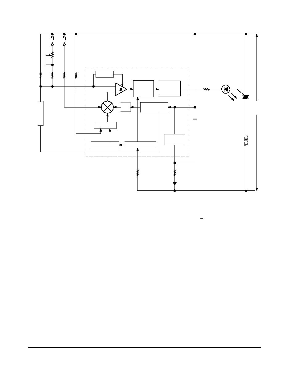
Representative Block Diagram
Sense Input
Sampling
Full Wave
Logic
+
≠
1/2
Failsafe
Hysteresis
Adjust
4
3
4≠Bit DAC
Temperature
Reduction
Voltage
Reference
Internal
Reference
+
1
+
VEE
5
Pulse
Amplifier
Supply
Voltage
+
Output
6
7
2
11≠Bit Counter
+VCC
Sync
UAA2016
8
Synchronization
This document contains information on a product under development. Motorola reserves the
right to change or discontinue this product without notice.
©
Motorola, Inc. 1996
Issue 5

UAA2016
2
MOTOROLA ANALOG IC DEVICE DATA
MAXIMUM RATINGS
(Voltages referenced to Pin 7)
Rating
Symbol
Value
Unit
Supply Current (IPin 5)
ICC
15
mA
Non≠Repetitive Supply Current
(Pulse Width = 1.0
µ
s)
ICCP
200
mA
AC Synchronization Current
Isync
3.0
mA
Pin Voltages
VPin 2
VPin 3
VPin 4
VPin 6
0; Vref
0; Vref
0; Vref
0; VEE
V
Vref Current Sink
IPin 1
1.0
mA
Output Current (Pin 6)
(Pulse Width < 400
µ
s)
IO
150
mA
Power Dissipation
PD
625
mW
Thermal Resistance, Junction≠to≠Air
R
JA
100
∞
C/W
Operating Temperature Range
TA
≠ 20 to + 85
∞
C
ELECTRICAL CHARACTERISTICS
(TA = 25
∞
C, VEE = ≠7.0 V, voltages referred to Pin 7, unless otherwise noted.)
Characteristic
Symbol
Min
Typ
Max
Unit
Supply Current (Pins 6, 8 not connected)
(TA = ≠ 20
∞
to + 85
∞
C)
ICC
--
0.9
1.5
mA
Stabilized Supply Voltage (Pin 5) (ICC = 2.0 mA)
VEE
≠10
≠ 9.0
≠ 8.0
V
Reference Voltage (Pin 1)
Vref
≠ 6.5
≠ 5.5
≠ 4.5
V
Output Pulse Current (TA = ≠ 20
∞
to + 85
∞
C)
(Rout = 60 W, VEE = ≠ 8.0 V)
IO
90
100
130
mA
Output Leakage Current (Vout = 0 V)
IOL
--
--
10
µ
A
Output Pulse Width (TA = ≠ 20
∞
to + 85
∞
C) (Note 1)
(Mains = 220 Vrms, Rsync = 220 k
)
TP
50
--
100
µ
s
Comparator Offset (Note 5)
Voff
≠10
--
+10
mV
Sensor Input Bias Current
IIB
--
--
0.1
µ
A
Sawtooth Period (Note 2)
TS
--
40.96
--
sec
Sawtooth Amplitude (Note 6)
AS
50
70
90
mV
Temperature Reduction Voltage (Note 3)
(Pin 4 Connected to VCC)
VTR
280
350
420
mV
Internal Hysteresis Voltage
(Pin 2 Not Connected)
VIH
--
10
--
mV
Additional Hysteresis (Note 4)
(Pin 2 Connected to VCC)
VH
280
350
420
mV
Failsafe Threshold (TA = ≠ 20
∞
to + 85
∞
C) (Note 7)
VFSth
180
--
300
mV
NOTES: 1. Output pulses are centered with respect to zero crossing point. Pulse width is adjusted by the value of Rsync. Refer to application curves.
2. The actual sawtooth period depends on the AC power line frequency. It is exactly 2048 times the corresponding period. For the 50 Hz case it is 40.96
sec. For the 60 Hz case it is 34.13 sec. This is to comply with the European standard, namely that 2.0 kW loads cannot be connected or removed
from the line more than once every 30 sec.
3. 350 mV corresponds to 5
∞
C temperature reduction. This is tested at probe using internal test pad. Smaller temperature reduction can be obtained by
adding an external resistor between Pin 4 and VCC. Refer to application curves.
4. 350 mV corresponds to a hysteresis of 5
∞
C. This is tested at probe using internal test pad. Smaller additional hysteresis can be obtained by adding
an external resistor between Pin 2 and VCC. Refer to application curves.
5. Parameter guaranteed but not tested. Worst case 10 mV corresponds to 0.15
∞
C shift on set point.
6. Measured at probe by internal test pad. 70 mV corresponds to 1
∞
C. Note that the proportional band is independent of the NTC value.
7. At very low temperature the NTC resistor increases quickly. This can cause the sensor input voltage to reach the failsafe threshold, thus inhibiting
output pulses; refer to application schematics. The corresponding temperature is the limit at which the circuit works in the typical application. By
setting this threshold at 0.05 Vref, the NTC value can increase up to 20 times its nominal value, thus the application works below ≠ 20
∞
C.
UAA2016
3
MOTOROLA ANALOG IC DEVICE DATA
Load
CF
MAC212A8
Rout
8
5
Rsync
VEE
Vref
Temp. Red.
Rdef
HysAdj
S2
RS
Figure 1. Application Schematic
R1
Synchronization
+
1
S1
R2
4
R3
≠
11≠Bit Counter
4≠Bit DAC
3
UAA2016
1/2
Failsafe
Pulse
Amplifier
Sampling
Full Wave
Logic
Internal
Reference
Supply
Voltage
2
+VCC
7
Output
6
RS
Sync
+
+
+
Sense Input
NTC
220 V
a
c
APPLICATION INFORMATION
(For simplicity, the LED in series with Rout is omitted in the
following calculations.)
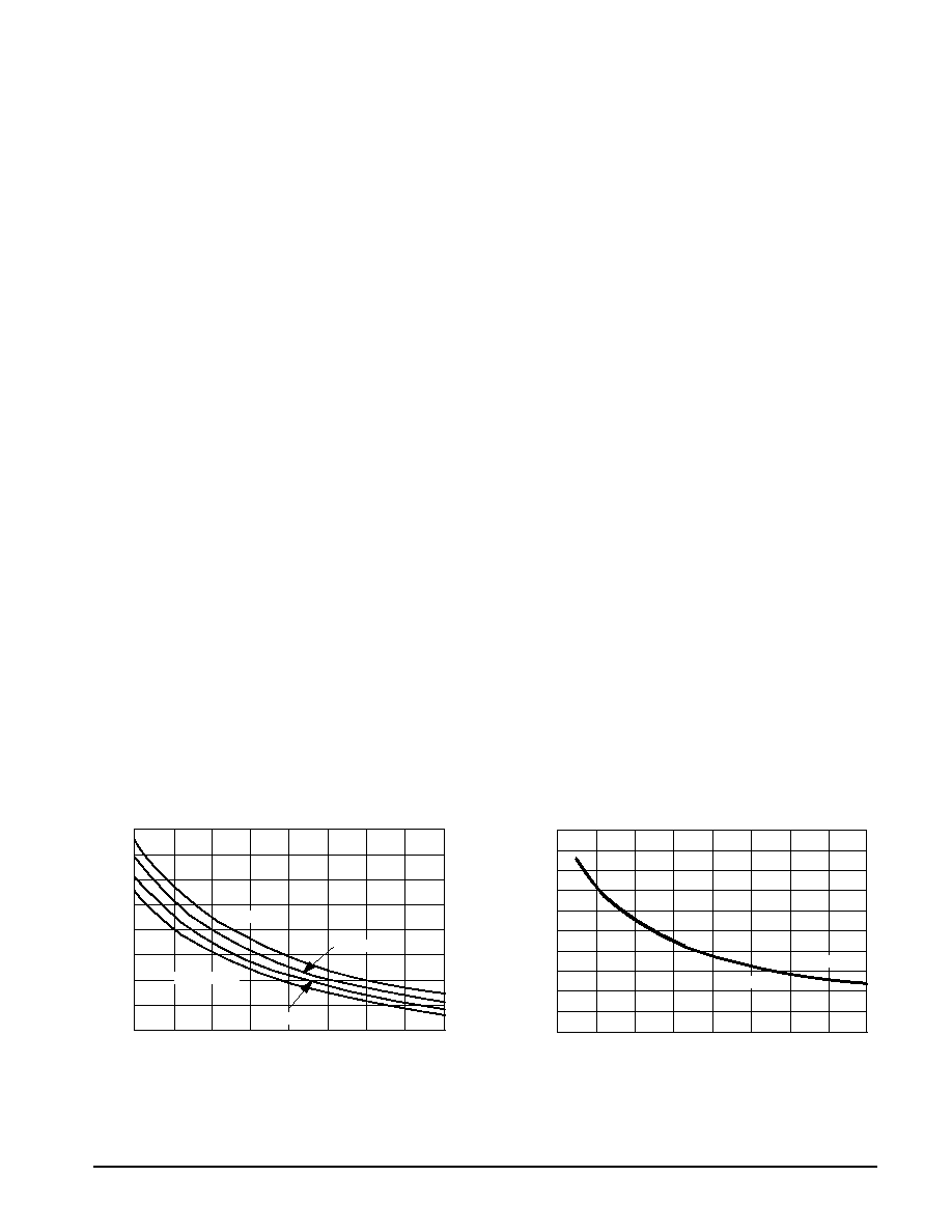
Triac Choice and Rout Determination
Depending on the power in the load, choose the triac that
has the lowest peak gate trigger current. This will limit the
output current of the UAA2016 and thus its power
consumption. Use Figure 4 to determine Rout according to
the triac maximum gate current (IGT) and the application low
temperature limit. For a 2.0 kW load at 220 Vrms, a good triac
choice is the Motorola MAC212A8. Its maximum peak gate
trigger current at 25
∞
C is 50 mA.
For an application to work down to ≠ 20
∞
C, Rout should be
60
. It is assumed that: IGT(T) = IGT(25
∞
C)
exp (≠T/125)
with T in
∞
C, which applies to the MAC212A8.
Output Pulse Width, Rsync
The pulse with TP is determined by the triac's IHold, ILatch
together with the load value and working conditions
(frequency and voltage):
Given the RMS AC voltage and the load power, the load
value is:
RL = V2rms/POWER
The load current is then:
I
Load
+
(Vrms
2
sin(2
p
ft)≠V
TM
) R
L
where VTM is the maximum on state voltage of the triac, f is
the line frequency.
Set ILoad = ILatch for t = TP/2 to calculate TP.
Figures 6 and 7 give the value of TP which corresponds to
the higher of the values of IHold and ILatch, assuming that
VTM = 1.6 V. Figure 8 gives the Rsync that produces the
corresponding TP.
RSupply and Filter Capacitor
With the output current and the pulse width determined as
above, use Figures 9 and 10 to determine RSupply, assuming
that the sinking current at Vref pin (including NTC bridge
current) is less than 0.5 mA. Then use Figure 11 and 12 to
determine the filter capacitor (CF) according to the ripple
desired on supply voltage. The maximum ripple allowed is
1.0 V.
Temperature Reduction Determined by R1
(Refer to Figures 13 and 14.)
UAA2016
4
MOTOROLA ANALOG IC DEVICE DATA
Figure 2. Comparison Between Proportional Control and ON/OFF Control
Overshoot
Time (minutes, Typ.)
Time (minutes, Typ.)
Time (minutes, Typ.)
Heating
Power
P(W)
Room
Temperature
T (
∞
C)
Time (minutes, Typ.)
Proportional Band
Proportional Temperature Control
D
Reduced Overshoot
D
Good Stability
ON/OFF Temperature Control
D
Large Overshoot
D
Marginal Stability
TP is centered on the zero≠crossing.
AC Line
Waveform
ILatch
TP
IHold
Figure 3. Zero Voltage Technique
Gate Current
Pulse
f = AC Line Frequency (Hz)
Vrms = AC Line RMS Voltage (V)
Rsync = Synchronization Resistor (
)
T
P
+
14 x Rsync
)
7
105
Vrms
2 x
p
f
(
µ
s)
UAA2016
5
MOTOROLA ANALOG IC DEVICE DATA
CIRCUIT FUNCTIONAL DESCRIPTION
Power Supply (Pin 5 and Pin 7)
The application uses a current source supplied by a single
high voltage rectifier in series with a power dropping resistor.
An integrated shunt regulator delivers a VEE voltage of
≠ 8.6 V with respect to Pin 7. The current used by the total
regulating system can be shared in four functional blocks: IC
supply, sensing bridge, triac gate firing pulses and zener
current. The integrated zener, as in any shunt regulator,
absorbs the excess supply current. The 50 Hz pulsed supply
current is smoothed by the large value capacitor connected
between Pins 5 and 7.
Temperature Sensing (Pin 3)
The actual temperature is sensed by a negative
temperature coefficient element connected in a resistor
divider fashion. This two element network is connected
between the ground terminal Pin 5 and the reference voltage
≠ 5.5 V available on Pin 1. The resulting voltage, a function of
the measured temperature, is applied to Pin 3 and internally
compared to a control voltage whose value depends on
several elements: Sawtooth, Temperature Reduction and
Hysteresis Adjust. (Refer to Application Information.)
Temperature Reduction
For energy saving, a remotely programmable temperature
reduction is available on Pin 4. The choice of resistor R1
connected between Pin 4 and VCC sets the temperature
reduction level.
Comparator
When the positive input (Pin 3) receives a voltage greater
than the internal reference value, the comparator allows the
triggering logic to deliver pulses to the triac gate. To improve
the noise immunity, the comparator has an adjustable
hysteresis. The external resistor R3 connected to Pin 2 sets
the hysteresis level. Setting Pin 2 open makes a 10 mV
hysteresis level, corresponding to 0.15
∞
C. Maximum
hysteresis is obtained by connecting Pin 2 to VCC. In that
case the level is set at 5
∞
C. This configuration can be useful
for low temperature inertia systems.
Sawtooth Generator
In order to comply with European norms, the ON/OFF
period on the load must exceed 30 seconds. This is achieved
by an internal digital sawtooth which performs the
proportional regulation without any additional component.
The sawtooth signal is added to the reference applied to the
comparator negative input. Figure 2 shows the regulation
improvement using the proportional band action.
Noise Immunity
The noisy environment requires good immunity. Both the
voltage reference and the comparator hysteresis minimize
the noise effect on the comparator input. In addition the
effective triac triggering is enabled every 1/3 sec.
Failsafe
Output pulses are inhibited by the "failsafe" circuit if the
comparator input voltage exceeds the specified threshold
voltage. This would occur if the temperature sensor circuit is
open.
Sampling Full Wave Logic
Two consecutive zero≠crossing trigger pulses are
generated at every positive mains half≠cycle. This ensures
that the number of delivered pulses is even in every case.
The pulse length is selectable by Rsync connected on Pin 8.
The pulse is centered on the zero≠crossing mains waveform.
Pulse Amplifier
The pulse amplifier circuit sinks current pulses from Pin 6
to VEE. The minimum amplitude is 70 mA. The triac is then
triggered in quadrants II and III. The effective output current
amplitude is given by the external resistor Rout. Eventually,
an LED can be inserted in series with the Triac gate (see
Figure 1).
TA = ≠ 20
∞
C
TA = 0
∞
C
140
80
200
Figure 4. Output Resistor versus
Triac Gate Current
IGT, TRIAC GATE CURRENT SPECIFIED AT 25
∞
C (mA)
20
60
160
180
40
50
40
30
60
120
100
R , OUTPUT
RESIST
OR ( )
out
Figure 5. Minimum Output Current
versus Output Resistor
TA = ≠ 20
∞
C
TA = + 85
∞
C
200
180
160
140
120
100
80
60
40
100
Rout, OUTPUT RESISTOR (
)
0
20
40
60
80
I , MINIMUM OUTPUT
CURRENT
(mA)
Out(min)
TA = +10
∞
C
TA = ≠10
∞
C