 | –≠–ª–µ–∫—Ç—Ä–æ–Ω–Ω—ã–π –∫–æ–º–ø–æ–Ω–µ–Ω—Ç: ULN2068 | –°–∫–∞—á–∞—Ç—å:  PDF PDF  ZIP ZIP |
Device
Operating
Temperature Range
Package
ULN2068
SEMICONDUCTOR
TECHNICAL DATA
QUAD 1.5 A
DARLINGTON SWITCH
ORDERING INFORMATION*
ULN2068B
TA = 0 to +70
∞
C
Plastic DIP
B SUFFIX
PLASTIC PACKAGE
CASE 648C
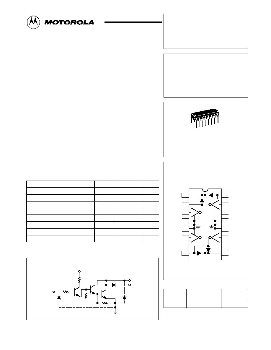
PIN CONNECTIONS
Order this document by ULN2068/D
K
C
B
Gnd
Gnd
VS
B
C
C
NC
B
Gnd
Gnd
B
C
K
1
2
3
4
5
6
7
8
16
15
14
13
12
11
10
9
*Other options of this ULN2060/2070 series are available
*
for volume applications. Contact your local Motorola Sales
*
Representative.
1
MOTOROLA ANALOG IC DEVICE DATA
Quad 1.5 A Sinking High
Current Switch
The ULN2068B is a high≠voltage, high≠current quad Darlington switch
array designed for high current loads, both resistive and reactive, up to 300 W.
It is intended for interfacing between low level (TTL, DTL, LS and 5.0 V
CMOS) logic families and peripheral loads such as relays, solenoids, dc and
stepping motors, multiplexer LED and incandescent displays, heaters, or other
high voltage, high current loads.
The Motorola ULN2068B is specified with minimum guaranteed breakdown
of 50 V and is 100% tested for safe area using an inductive load. It includes
integral transient suppression diodes. Use of a predriver stage reduces input
current while still allowing the device to switch 1.5 Amps.
It is supplied in an improved 16≠Pin plastic DIP package with heat sink
contact tabs (Pins 4, 5, 12 and 13). A copper alloy lead frame allows maximum
power dissipation using standard cooling techniques. The use of the contact
tab lead frame facilitates attachment of a DIP heat sink while permitting the
use of standard layout and mounting practices.
∑
TTL, DTL, LS, CMOS Compatible Inputs
∑
1.5 A Maximum Output Current
∑
Low Input Current
∑
Internal Freewheeling Clamp Diodes
∑
100% Inductive Load Tested
∑
Heat Tab Copper Alloy Lead Frame for Increased Dissipation
MAXIMUM RATINGS
(TA = 25
∞
C and ratings apply to any one device in the
package, unless otherwise noted)
Rating
Symbol
Value
Unit
Output Voltage
VO
50
V
Input Voltage (Note 1)
VI
15
V
Supply Voltage
VS
10
V
Collector Current (Note 2)
IC
1.75
A
Input Current (Note 3)
II
25
mA
Operating Ambient Temperature Range
TA
0 to +70
∞
C
Storage Temperature Range
Tstg
≠55 to +150
∞
C
Junction Temperature
TJ
150
∞
C
NOTES: 1. Input voltage referenced to ground.
2. Allowable output conditions shown in Figures 11 and 12.
3. May be limited by max input voltage.
Partial Schematic
C
3.0 k
7.2 k
RS
0.9 k
B
Rin
2.5 k
VS
K
©
Motorola, Inc. 1995

ULN2068
2
MOTOROLA ANALOG IC DEVICE DATA
ELECTRICAL CHARACTERISTICS
(TA = 25
∞
C unless otherwise noted.)
Characteristic
Symbol
Min
Typ
Max
Unit
Output Leakage Current (Figure 1)
(VCE = 50 V)
(VCE = 50 V, TA = 70
∞
C)
ICEX
≠
≠
≠
≠
100
500
µ
A
Collector≠Emitter Saturation Voltage (Figure 2)
(IC = 500 mA
(IC = 750 mA
(IC = 1.0 A
(IC = 1.25 A
Vin = 2.4 V)
VCE(sat)
≠
≠
≠
≠
≠
≠
≠
≠
1.13
1.25
1.40
1.60
V
Input Current ≠ On Condition (Figure 4)
(VI = 2.4 V)
(VI = 3.75 V)
II(on)
≠
≠
≠
≠
0.25
1.0
mA
Input Voltage ≠ On Condition (Figure 5)
(VCE = 2.0 V, IC = 1.5 A)
VI(on)
≠
≠
2.4
V
Inductive Load Test (Figure 3)
(VS = 5.5 V, VCC = 24.5 V,
tPW = 4.0 ms)
Vout
≠
≠
100
mV
Supply Current (Figure 8)
(IC = 500 mA, Vin = 2.4 V, VS = 5.5 V)
IS
≠
≠
6.0
mA
Turn≠On Delay Time
(50% EI to 50% EO)
tPHL
≠
≠
1.0
µ
s
Turn≠Off Delay Time
(50% EI to 50% EO)
tPLH
≠
≠
4.0
µ
s
Clamp Diode Leakage Current (Figure 6)
(VR = 50 V)
(VR = 50 V, TA = 70
∞
C)
IR
≠
≠
≠
≠
50
100
µ
A
Clamp Diode Forward Voltage (Figure 7)
(IF = 1.0 A)
(IF = 1.5 A)
VF
≠
≠
≠
≠
1.75
2.0
V
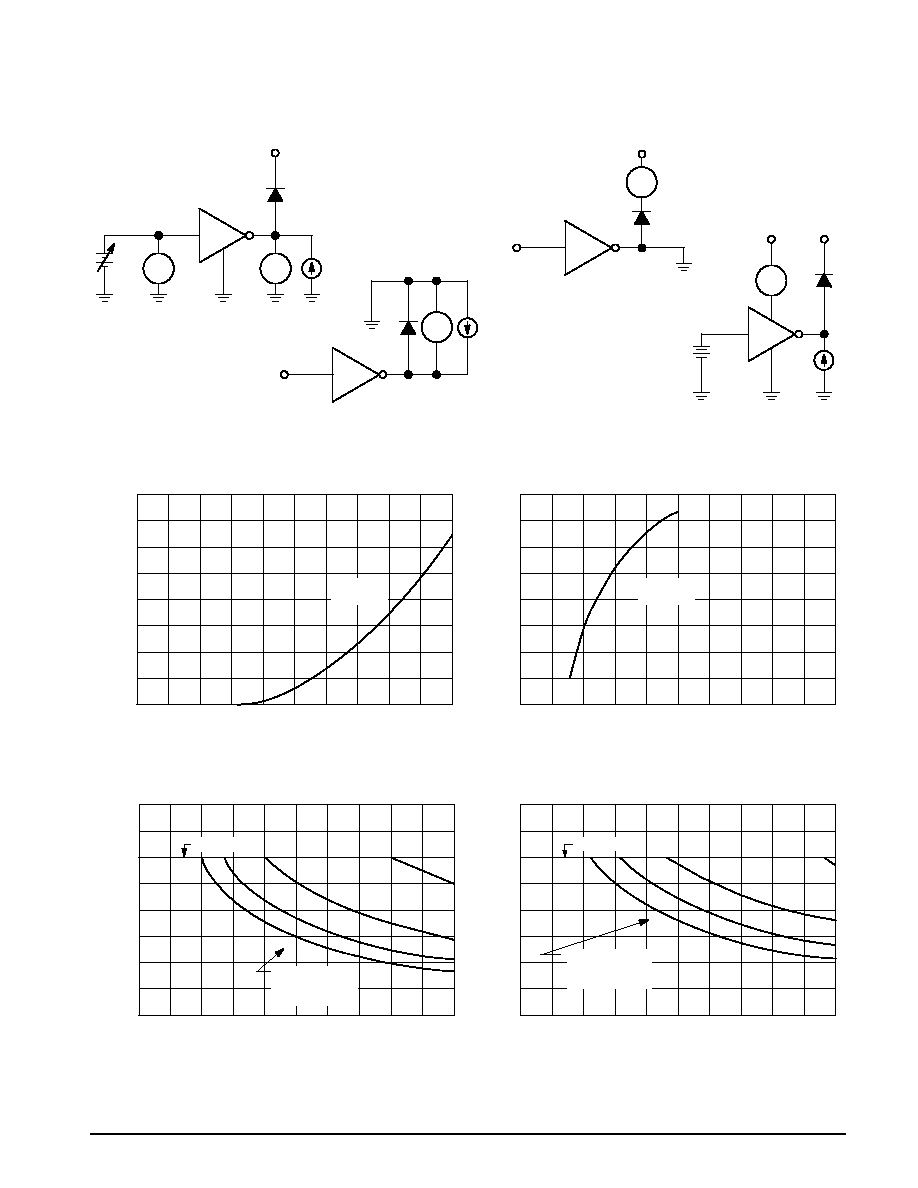
TEST FIGURES
9
70 MH
20
VCC
VS
tPW
IC
Iin
Vout =
Vout1 ≠ Vout2
VCE
Open
µ
A
Open
ICEX
0
DUT
14 ms
5.0
V
Vin
Open
VCE
DUT
Vin
DUT
DUT
mA
Open
Vin
Open
Vout
1
Vout
2
Figure 1.
Figure 2.
Figure 3.
Figure 4.
ULN2068
3
MOTOROLA ANALOG IC DEVICE DATA
Vin, INPUT VOLTAGE (V)
VS = 5.0 V
TA = 25
∞
C
0
1.0
2.0
3.0
4.0
IS
II, INPUT CURRENT (mA)
4
2
3
1.0
100
40
5.0
0
Device Limit
Number of
outputs conducting
simultaneously
DUTY CYCLE (%)
1
0
20
60
80
0.5
1.5
TYPICAL CHARACTERISTIC CURVES ≠ TA = 25
∞
C
TEST FIGURES (continued)
Figure 5.
IC
VCE
Open
µ
A
DUT
V
Vin
Open
V
DUT
Open
IF
V
VF
IR
mA
VR
Vin
DUT
DUT
Open
VS
IC
I , INPUT
CURRENT
(A)
I
I , COLLECT
OR CURRENT
(A)
C
VS = 5.0 V
TA = 25
∞
C
0
1.0
2.0
3.0
4.0
0
1.6
1.4
1.2
1.0
0.8
0.6
0.4
0.2
Device Limit
4
2
3
1
0
1.6
1.4
1.2
1.0
0.8
0.6
0.4
0.2
1.0
0
0.5
1.5
100
40
DUTY CYCLE (%)
0
20
60
80
I ,
ALLOW
ABLE PEAK
COLLECT
OR CURRENT
(A)
C
I ,
ALLOW
ABLE PEAK
COLLECT
OR CURRENT
(A)
C
Number of
outputs conducting
simultaneously
Figure 6.
Figure 7.
Figure 8.
Figure 9. Input Current
versus Input Voltage
Figure 10. Collector Current
versus Input Current
Figure 11. TA = 70
∞
C w/o Heat Sink
Figure 12. TA = 70
∞
C w/Staver V≠8
Heat Sink (37.5
∞
C/W)

ULN2068
4
MOTOROLA ANALOG IC DEVICE DATA
3
4
2
1
Device Limit
Number of
outputs conducting
simultaneously
100
80
60
40
20
0
0
0.5
1.0
1.5
DUTY CYCLE (%)
I ,
ALLOW
ABLE PEAK
COLLECT
OR CURRENT
(A)
C
Number of
outputs conducting
simultaneously
Device Limit
Device Limit
Device Limit
I ,
ALLOW
ABLE PEAK
COLLECT
OR CURRENT
(A)
C
I ,
ALLOW
ABLE PEAK
COLLECT
OR CURRENT
(A)
C
I ,
ALLOW
ABLE PEAK
COLLECT
OR CURRENT
(A)
C
100
80
60
40
20
0
100
80
60
40
20
0
100
80
60
40
20
0
0
0.5
1.0
1.5
0
0.5
1.0
1.5
0
0.5
1.0
1.5
DUTY CYCLE (%)
DUTY CYCLE (%)
DUTY CYCLE (%)
3
4
2
1
3
4
2
1
3
4
2
1
Number of
outputs conducting
simultaneously
Number of
outputs conducting
simultaneously
Figure 13. TA = 70
∞
C w/Staver V≠7
Heat Sink (27.5
∞
C/W)
Figure 14. TA = 50
∞
C w/o Heat Sink
Figure 15. TA = 50
∞
C w/Staver V≠8
Heat Sink (37.5
∞
C/W)
Figure 16. TA = 50
∞
C w/Staver V≠7
Heat Sink (27.5
∞
C/W)
ULN2068
5
MOTOROLA ANALOG IC DEVICE DATA
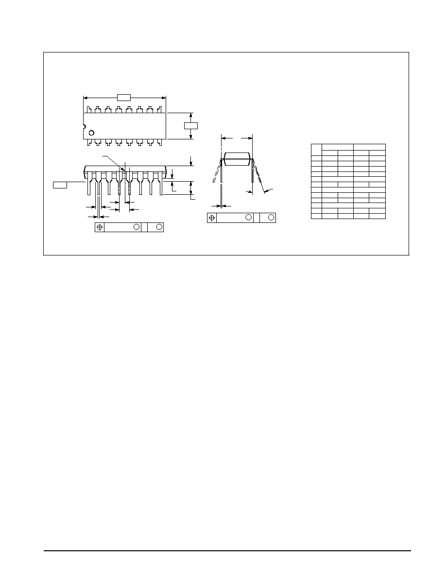
OUTLINE DIMENSIONS
DIM
MIN
MAX
MIN
MAX
MILLIMETERS
INCHES
A
0.740
0.840
18.80
21.34
B
0.240
0.260
6.10
6.60
C
0.145
0.185
3.69
4.69
D
0.015
0.021
0.38
0.53
E
0.050 BSC
1.27 BSC
F
0.040
0.70
1.02
1.78
G
0.100 BSC
2.54 BSC
J
0.008
0.015
0.20
0.38
K
0.115
0.135
2.92
3.43
L
0.300 BSC
7.62 BSC
M
0
10
0
10
N
0.015
0.040
0.39
1.01
_
_
_
_
NOTES:
1. DIMENSIONING AND TOLERANCING PER ANSI
Y14.5M, 1982.
2. CONTROLLING DIMENSION: INCH.
3. DIMENSION L TO CENTER OF LEADS WHEN
FORMED PARALLEL.
4. DIMENSION B DOES NOT INCLUDE MOLD FLASH.
5. INTERNAL LEAD CONNECTION BETWEEN 4 AND
5, 12 AND 13.
≠A≠
≠B≠
16
9
1
8
F
D
G
E
N
C
NOTE 5
16 PL
S
A
M
0.13 (0.005)
T
≠T≠
SEATING
PLANE
S
B
M
0.13 (0.005)
T
J
16 PL
M
L
B SUFFIX
PLASTIC PACKAGE
CASE 648C≠03
ISSUE C
ULN2068
6
MOTOROLA ANALOG IC DEVICE DATA
Motorola reserves the right to make changes without further notice to any products herein. Motorola makes no warranty, representation or guarantee regarding
the suitability of its products for any particular purpose, nor does Motorola assume any liability arising out of the application or use of any product or circuit,
and specifically disclaims any and all liability, including without limitation consequential or incidental damages. "Typical" parameters can and do vary in different
applications. All operating parameters, including "Typicals" must be validated for each customer application by customer's technical experts. Motorola does
not convey any license under its patent rights nor the rights of others. Motorola products are not designed, intended, or authorized for use as components in
systems intended for surgical implant into the body, or other applications intended to support or sustain life, or for any other application in which the failure of
the Motorola product could create a situation where personal injury or death may occur. Should Buyer purchase or use Motorola products for any such
unintended or unauthorized application, Buyer shall indemnify and hold Motorola and its officers, employees, subsidiaries, affiliates, and distributors harmless
against all claims, costs, damages, and expenses, and reasonable attorney fees arising out of, directly or indirectly, any claim of personal injury or death
associated with such unintended or unauthorized use, even if such claim alleges that Motorola was negligent regarding the design or manufacture of the part.
Motorola and
are registered trademarks of Motorola, Inc. Motorola, Inc. is an Equal Opportunity/Affirmative Action Employer.
How to reach us:
USA / EUROPE: Motorola Literature Distribution;
JAPAN: Nippon Motorola Ltd.; Tatsumi≠SPD≠JLDC, Toshikatsu Otsuki,
P.O. Box 20912; Phoenix, Arizona 85036. 1≠800≠441≠2447
6F Seibu≠Butsuryu≠Center, 3≠14≠2 Tatsumi Koto≠Ku, Tokyo 135, Japan. 03≠3521≠8315
MFAX: RMFAX0@email.sps.mot.com ≠ TOUCHTONE (602) 244≠6609
HONG KONG: Motorola Semiconductors H.K. Ltd.; 8B Tai Ping Industrial Park,
INTERNET: http://Design≠NET.com
51 Ting Kok Road, Tai Po, N.T., Hong Kong. 852≠26629298
ULN2068/D
*ULN2068/D*